
ADC12DJ3200 Datasheet - TI. · PDF fileInput Frequency (GHz) Normalized Gain Response (dB) 0 2...
155
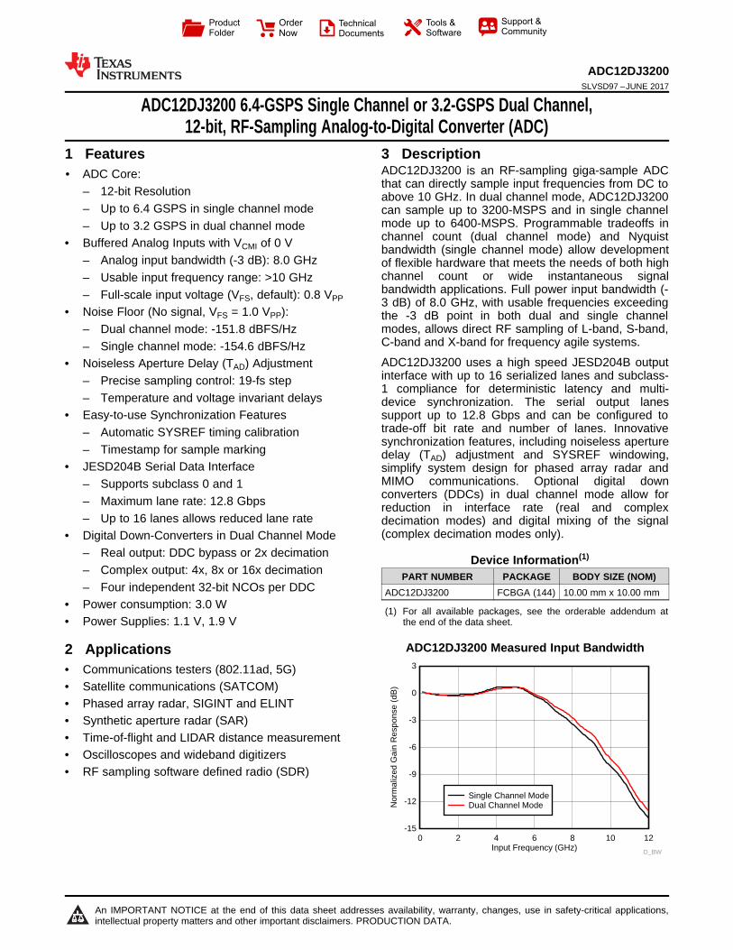
Input Frequency (GHz) Normalized Gain Response (dB) 0 2 4 6 8 10 12 -15 -12 -9 -6 -3 0 3 D_BW Single Channel Mode Dual Channel Mode Product Folder Order Now Technical Documents Tools & Software Support & Community An IMPORTANT NOTICE at the end of this data sheet addresses availability, warranty, changes, use in safety-critical applications, intellectual property matters and other important disclaimers. PRODUCTION DATA. ADC12DJ3200 SLVSD97 – JUNE 2017 ADC12DJ3200 6.4-GSPS Single Channel or 3.2-GSPS Dual Channel, 12-bit, RF-Sampling Analog-to-Digital Converter (ADC) 1 1 Features 1• ADC Core: – 12-bit Resolution – Up to 6.4 GSPS in single channel mode – Up to 3.2 GSPS in dual channel mode • Buffered Analog Inputs with V CMI of 0 V – Analog input bandwidth (-3 dB): 8.0 GHz – Usable input frequency range: >10 GHz – Full-scale input voltage (V FS , default): 0.8 V PP • Noise Floor (No signal, V FS = 1.0 V PP ): – Dual channel mode: -151.8 dBFS/Hz – Single channel mode: -154.6 dBFS/Hz • Noiseless Aperture Delay (T AD ) Adjustment – Precise sampling control: 19-fs step – Temperature and voltage invariant delays • Easy-to-use Synchronization Features – Automatic SYSREF timing calibration – Timestamp for sample marking • JESD204B Serial Data Interface – Supports subclass 0 and 1 – Maximum lane rate: 12.8 Gbps – Up to 16 lanes allows reduced lane rate • Digital Down-Converters in Dual Channel Mode – Real output: DDC bypass or 2x decimation – Complex output: 4x, 8x or 16x decimation – Four independent 32-bit NCOs per DDC • Power consumption: 3.0 W • Power Supplies: 1.1 V, 1.9 V 2 Applications • Communications testers (802.11ad, 5G) • Satellite communications (SATCOM) • Phased array radar, SIGINT and ELINT • Synthetic aperture radar (SAR) • Time-of-flight and LIDAR distance measurement • Oscilloscopes and wideband digitizers • RF sampling software defined radio (SDR) 3 Description ADC12DJ3200 is an RF-sampling giga-sample ADC that can directly sample input frequencies from DC to above 10 GHz. In dual channel mode, ADC12DJ3200 can sample up to 3200-MSPS and in single channel mode up to 6400-MSPS. Programmable tradeoffs in channel count (dual channel mode) and Nyquist bandwidth (single channel mode) allow development of flexible hardware that meets the needs of both high channel count or wide instantaneous signal bandwidth applications. Full power input bandwidth (- 3 dB) of 8.0 GHz, with usable frequencies exceeding the -3 dB point in both dual and single channel modes, allows direct RF sampling of L-band, S-band, C-band and X-band for frequency agile systems. ADC12DJ3200 uses a high speed JESD204B output interface with up to 16 serialized lanes and subclass- 1 compliance for deterministic latency and multi- device synchronization. The serial output lanes support up to 12.8 Gbps and can be configured to trade-off bit rate and number of lanes. Innovative synchronization features, including noiseless aperture delay (T AD ) adjustment and SYSREF windowing, simplify system design for phased array radar and MIMO communications. Optional digital down converters (DDCs) in dual channel mode allow for reduction in interface rate (real and complex decimation modes) and digital mixing of the signal (complex decimation modes only). Device Information (1) PART NUMBER PACKAGE BODY SIZE (NOM) ADC12DJ3200 FCBGA (144) 10.00 mm x 10.00 mm (1) For all available packages, see the orderable addendum at the end of the data sheet. ADC12DJ3200 Measured Input Bandwidth
Transcript of ADC12DJ3200 Datasheet - TI. · PDF fileInput Frequency (GHz) Normalized Gain Response (dB) 0 2...
Input Frequency (GHz)
Nor
mal
ized
Gai
n R
espo
nse
(dB
)
0 2 4 6 8 10 12-15
-12
-9
-6
-3
0
3
D_BW
Single Channel ModeDual Channel Mode
Product
Folder
Order
Now
Technical
Documents
Tools &
Software
Support &Community
An IMPORTANT NOTICE at the end of this data sheet addresses availability, warranty, changes, use in safety-critical applications,intellectual property matters and other important disclaimers. PRODUCTION DATA.
ADC12DJ3200SLVSD97 –JUNE 2017
ADC12DJ3200 6.4-GSPS Single Channel or 3.2-GSPS Dual Channel,12-bit, RF-Sampling Analog-to-Digital Converter (ADC)
1
1 Features1• ADC Core:
– 12-bit Resolution– Up to 6.4 GSPS in single channel mode– Up to 3.2 GSPS in dual channel mode
• Buffered Analog Inputs with VCMI of 0 V– Analog input bandwidth (-3 dB): 8.0 GHz– Usable input frequency range: >10 GHz– Full-scale input voltage (VFS, default): 0.8 VPP
• Noise Floor (No signal, VFS = 1.0 VPP):– Dual channel mode: -151.8 dBFS/Hz– Single channel mode: -154.6 dBFS/Hz
• Noiseless Aperture Delay (TAD) Adjustment– Precise sampling control: 19-fs step– Temperature and voltage invariant delays
• Easy-to-use Synchronization Features– Automatic SYSREF timing calibration– Timestamp for sample marking
• JESD204B Serial Data Interface– Supports subclass 0 and 1– Maximum lane rate: 12.8 Gbps– Up to 16 lanes allows reduced lane rate
• Digital Down-Converters in Dual Channel Mode– Real output: DDC bypass or 2x decimation– Complex output: 4x, 8x or 16x decimation– Four independent 32-bit NCOs per DDC
• Power consumption: 3.0 W• Power Supplies: 1.1 V, 1.9 V
2 Applications• Communications testers (802.11ad, 5G)• Satellite communications (SATCOM)• Phased array radar, SIGINT and ELINT• Synthetic aperture radar (SAR)• Time-of-flight and LIDAR distance measurement• Oscilloscopes and wideband digitizers• RF sampling software defined radio (SDR)
3 DescriptionADC12DJ3200 is an RF-sampling giga-sample ADCthat can directly sample input frequencies from DC toabove 10 GHz. In dual channel mode, ADC12DJ3200can sample up to 3200-MSPS and in single channelmode up to 6400-MSPS. Programmable tradeoffs inchannel count (dual channel mode) and Nyquistbandwidth (single channel mode) allow developmentof flexible hardware that meets the needs of both highchannel count or wide instantaneous signalbandwidth applications. Full power input bandwidth (-3 dB) of 8.0 GHz, with usable frequencies exceedingthe -3 dB point in both dual and single channelmodes, allows direct RF sampling of L-band, S-band,C-band and X-band for frequency agile systems.
ADC12DJ3200 uses a high speed JESD204B outputinterface with up to 16 serialized lanes and subclass-1 compliance for deterministic latency and multi-device synchronization. The serial output lanessupport up to 12.8 Gbps and can be configured totrade-off bit rate and number of lanes. Innovativesynchronization features, including noiseless aperturedelay (TAD) adjustment and SYSREF windowing,simplify system design for phased array radar andMIMO communications. Optional digital downconverters (DDCs) in dual channel mode allow forreduction in interface rate (real and complexdecimation modes) and digital mixing of the signal(complex decimation modes only).
Device Information(1)
PART NUMBER PACKAGE BODY SIZE (NOM)ADC12DJ3200 FCBGA (144) 10.00 mm x 10.00 mm
(1) For all available packages, see the orderable addendum atthe end of the data sheet.
ADC12DJ3200 Measured Input Bandwidth

2
ADC12DJ3200SLVSD97 –JUNE 2017 www.ti.com
Product Folder Links: ADC12DJ3200
Submit Documentation Feedback Copyright © 2017, Texas Instruments Incorporated
Table of Contents1 Features .................................................................. 12 Applications ........................................................... 13 Description ............................................................. 14 Revision History..................................................... 25 Pin Configuration and Functions ......................... 36 Specifications......................................................... 9
6.1 Absolute Maximum Ratings ...................................... 96.2 ESD Ratings.............................................................. 96.3 Recommended Operating Conditions..................... 106.4 Thermal Information ................................................ 116.5 Electrical Characteristics - DC Specifications......... 126.6 Electrical Characteristics - Power Consumption..... 146.7 Electrical Characteristics - AC Specifications ......... 156.8 Timing Requirements .............................................. 226.9 Switching Characteristics ........................................ 236.10 Typical Characteristics .......................................... 27
7 Detailed Description ............................................ 387.1 Overview ................................................................. 387.2 Functional Block Diagrams ..................................... 397.3 Feature Description................................................. 397.4 Device Functional Modes........................................ 61
7.5 Programming........................................................... 797.6 Register Maps ......................................................... 80
8 Application and Implementation ...................... 1378.1 Application Information.......................................... 1378.2 Typical Application ............................................... 1378.3 Initialization Set Up .............................................. 140
9 Power Supply Recommendations .................... 14010 Layout................................................................. 142
10.1 Layout Guidelines ............................................... 14210.2 Layout Example .................................................. 143
11 Device and Documentation Support ............... 14611.1 Device Support .................................................. 14611.2 Related Links ...................................................... 14611.3 Receiving Notification of Documentation
Updates.................................................................. 14611.4 Community Resources........................................ 14611.5 Trademarks ......................................................... 14611.6 Electrostatic Discharge Caution.......................... 14611.7 Glossary .............................................................. 146
12 Mechanical, Packaging, and OrderableInformation ......................................................... 147
4 Revision HistoryNOTE: Page numbers for previous revisions may differ from page numbers in the current version.
DATE REVISION NOTESMay 2017 * Advance Information releaseJune 2017 * Production Data release

AGND
TMSTP+
INA+
TMSTP- SYNCSE BG VA19
VA19
INA- DA3+
VA11 NCOA0 ORA0
NCOA1 ORA1
DA3- DA2+ DA2-
DA5+ DA1+
DA5- DA1-
VA19
CLK+
VA19 VA19
VA19
CLK-
VA19
VA19
VA19 VA19
CALTRIG SCS
CALSTAT SCLK
SDI
SDO
DA4+ DA0+
DA4- DA0-
DB4- DB0-
DB4+ DB0+
SYSREF+ TDIODE+
VA19
TDIODE- VA19
SYSREF-
INB+
PD
NCOB1 ORB1
NCOB0 ORB0
INB-
DB7+
DB3+
DB5- DB1-
DB5+ DB1+
DB7- DB6+
DB3- DB2+
DB6-
DB2-
A
B
C
D
E
F
G
H
J
K
L
M
121110987654321
AGND AGND
AGND AGND AGND AGND
AGND AGND
AGND AGND
AGND AGND
AGND AGND
AGND AGND AGND
AGND AGND AGND AGND AGND AGND
AGND AGND
AGND
AGND
AGND
AGND
AGND
AGND
AGND
AGND
AGND
AGND
DGND
DGND
DGND DGND
DGND DGND
DGND DGND
DGND DGND
DGND
DGND
VA11
VA11
VA11
VA11
VA11
VA11
VA11
VA11 VA11
VA11 VA11
VD11 VD11
VD11 VD11
VD11 VD11
VD11 VD11
DA7+ DA7- DA6+ DA6-
AGND
VD11
VD11
3
ADC12DJ3200www.ti.com SLVSD97 –JUNE 2017
Product Folder Links: ADC12DJ3200
Submit Documentation FeedbackCopyright © 2017, Texas Instruments Incorporated
5 Pin Configuration and Functions
AAV Package144-Ball Flip Chip BGA
Top View
4
ADC12DJ3200SLVSD97 –JUNE 2017 www.ti.com
Product Folder Links: ADC12DJ3200
Submit Documentation Feedback Copyright © 2017, Texas Instruments Incorporated
Pin FunctionsPIN
I/O DESCRIPTIONNAME NO.
AGND
A1, A2, A3,A6, A7, B2,B3, B4, B5,B6, B7, C6,D1, D6, E1,E6, F2, F3,F6, G2, G3,G6, H1, H6,J1, J6, L2,L3, L4, L5,L6, L7, M1,M2, M3, M6,
M7
— Analog supply ground. AGND and DGND should be tied to a common ground plane (GND)on circuit board.
DGND
A12, B12,D9, D10, F9,
F10, G9,G10, J9, J10,
L12, M12
— Digital supply ground. AGND and DGND should be tied to a common ground plane (GND)on circuit board.
BG C3 OBandgap voltage output. This pin is capable of sourcing only small currents and drivinglimited capacitive loads as specified in Recommended Operating Conditions. This pin can beleft disconnected if not used.
CALSTAT F7 O Foreground calibration status output or device alarm output. Functionality is programmedthrough CAL_STATUS_SEL. This pin can be left disconnected if not used.
CALTRIG E7 IForeground calibration trigger input. This pin is only used if hardware calibration triggering isselected in CAL_TRIG_EN, otherwise software triggering is performed usingCAL_SOFT_TRIG. This pin should be tied to GND if not used.
CLK+ F1 I
Device (sampling) clock positive input. The clock signal is strongly recommended to be ACcoupled to this input for best performance. In single channel mode, the analog input signal issampled on both rising and falling edges. In dual channel mode, the analog signal issampled on the rising edge. This differential input has an internal untrimmed 100-Ωdifferential termination and is self-biased to the optimal input common mode voltage as longas DEVCLK_LVPECL_EN is set to 0.
CLK- G1 I Device (sampling) clock negative input. Strongly recommended to use AC coupling for bestperformance.
DA0+ E12 O
High-speed serialized-data output for channel A, lane 0, positive connection. This differentialoutput must be AC-coupled and should always be terminated with a 100-Ω differentialtermination at the receiver. This pin can be left disconnected if not used. See note beneathRecommended Operating Conditions for information regarding reliable serializer operation.
DA0- F12 OHigh-speed serialized-data output for channel A, lane 0, negative connection. This pin canbe left disconnected if not used. See note beneath Recommended Operating Conditions forinformation regarding reliable serializer operation.
DA1+ C12 O
High-speed serialized-data output for channel A, lane 1, positive connection. This differentialoutput must be AC-coupled and must always be terminated with a 100-Ω differentialtermination at the receiver. This pin can be left disconnected if not used. See note beneathRecommended Operating Conditions for information regarding reliable serializer operation.
DA1- D12 OHigh-speed serialized-data output for channel A, lane 1, negative connection. This pin canbe left disconnected if not used. See note beneath Recommended Operating Conditions forinformation regarding reliable serializer operation.
DA2+ A10 O
High-speed serialized-data output for channel A, lane 2, positive connection. This differentialoutput must be AC-coupled and must always be terminated with a 100-Ω differentialtermination at the receiver. This pin can be left disconnected if not used. See note beneathRecommended Operating Conditions for information regarding reliable serializer operation.
DA2- A11 OHigh-speed serialized-data output for channel A, lane 2, negative connection. This pin canbe left disconnected if not used. See note beneath Recommended Operating Conditions forinformation regarding reliable serializer operation.
DA3+ A8 O
High-speed serialized-data output for channel A, lane 3, positive connection. This differentialoutput must be AC-coupled and must always be terminated with a 100-Ω differentialtermination at the receiver. This pin can be left disconnected if not used. See note beneathRecommended Operating Conditions for information regarding reliable serializer operation.

5
ADC12DJ3200www.ti.com SLVSD97 –JUNE 2017
Product Folder Links: ADC12DJ3200
Submit Documentation FeedbackCopyright © 2017, Texas Instruments Incorporated
Pin Functions (continued)PIN
I/O DESCRIPTIONNAME NO.
DA3- A9 OHigh-speed serialized-data output for channel A, lane 3, negative connection. This pin canbe left disconnected if not used. See note beneath Recommended Operating Conditions forinformation regarding reliable serializer operation.
DA4+ E11 O
High-speed serialized-data output for channel A, lane 4, positive connection. This differentialoutput must be AC-coupled and must always be terminated with a 100-Ω differentialtermination at the receiver. This pin can be left disconnected if not used. See note beneathRecommended Operating Conditions for information regarding reliable serializer operation.
DA4- F11 OHigh-speed serialized-data output for channel A, lane 4, negative connection. This pin canbe left disconnected if not used. See note beneath Recommended Operating Conditions forinformation regarding reliable serializer operation.
DA5+ C11 O
High-speed serialized-data output for channel A, lane 5, positive connection. This differentialoutput must be AC-coupled and must always be terminated with a 100-Ω differentialtermination at the receiver. This pin can be left disconnected if not used. See note beneathRecommended Operating Conditions for information regarding reliable serializer operation.
DA5- D11 OHigh-speed serialized-data output for channel A, lane 5, negative connection. This pin canbe left disconnected if not used. See note beneath Recommended Operating Conditions forinformation regarding reliable serializer operation.
DA6+ B10 O
High-speed serialized-data output for channel A, lane 6, positive connection. This differentialoutput must be AC-coupled and must always be terminated with a 100-Ω differentialtermination at the receiver. This pin can be left disconnected if not used. See note beneathRecommended Operating Conditions for information regarding reliable serializer operation.
DA6- B11 OHigh-speed serialized-data output for channel A, lane 6, negative connection. This pin canbe left disconnected if not used. See note beneath Recommended Operating Conditions forinformation regarding reliable serializer operation.
DA7+ B8 O
High-speed serialized-data output for channel A, lane 7, positive connection. This differentialoutput must be AC-coupled and must always be terminated with a 100-Ω differentialtermination at the receiver. This pin can be left disconnected if not used. See note beneathRecommended Operating Conditions for information regarding reliable serializer operation.
DA7- B9 OHigh-speed serialized-data output for channel A, lane 7, negative connection. This pin canbe left disconnected if not used. See note beneath Recommended Operating Conditions forinformation regarding reliable serializer operation.
DB0+ H12 O
High-speed serialized-data output for channel B, lane 0, positive connection. This differentialoutput must be AC-coupled and must always be terminated with a 100-Ω differentialtermination at the receiver. This pin can be left disconnected if not used. See note beneathRecommended Operating Conditions for information regarding reliable serializer operation.
DB0- G12 OHigh-speed serialized-data output for channel B, lane 0, negative connection. This pin canbe left disconnected if not used. See note beneath Recommended Operating Conditions forinformation regarding reliable serializer operation.
DB1+ K12 O
High-speed serialized-data output for channel B, lane 1, positive connection. This differentialoutput must be AC-coupled and must always be terminated with a 100-Ω differentialtermination at the receiver. This pin can be left disconnected if not used. See note beneathRecommended Operating Conditions for information regarding reliable serializer operation.
DB1- J12 OHigh-speed serialized-data output for channel B, lane 1, negative connection. This pin canbe left disconnected if not used. See note beneath Recommended Operating Conditions forinformation regarding reliable serializer operation.
DB2+ M10 O
High-speed serialized-data output for channel B, lane 2, positive connection. This differentialoutput must be AC-coupled and must always be terminated with a 100-Ω differentialtermination at the receiver. This pin can be left disconnected if not used. See note beneathRecommended Operating Conditions for information regarding reliable serializer operation.
DB2- M11 OHigh-speed serialized-data output for channel B, lane 2, negative connection. This pin canbe left disconnected if not used. See note beneath Recommended Operating Conditions forinformation regarding reliable serializer operation.
DB3+ M8 O
High-speed serialized-data output for channel B, lane 3, positive connection. This differentialoutput must be AC-coupled and must always be terminated with a 100-Ω differentialtermination at the receiver. This pin can be left disconnected if not used. See note beneathRecommended Operating Conditions for information regarding reliable serializer operation.
DB3- M9 OHigh-speed serialized-data output for channel B, lane 3, negative connection. This pin canbe left disconnected if not used. See note beneath Recommended Operating Conditions forinformation regarding reliable serializer operation.
6
ADC12DJ3200SLVSD97 –JUNE 2017 www.ti.com
Product Folder Links: ADC12DJ3200
Submit Documentation Feedback Copyright © 2017, Texas Instruments Incorporated
Pin Functions (continued)PIN
I/O DESCRIPTIONNAME NO.
DB4+ H11 O
High-speed serialized-data output for channel B, lane 4, positive connection. This differentialoutput must be AC-coupled and must always be terminated with a 100-Ω differentialtermination at the receiver. This pin can be left disconnected if not used. See note beneathRecommended Operating Conditions for information regarding reliable serializer operation.
DB4- G11 OHigh-speed serialized-data output for channel B, lane 4, negative connection. This pin canbe left disconnected if not used. See note beneath Recommended Operating Conditions forinformation regarding reliable serializer operation.
DB5+ K11 O
High-speed serialized-data output for channel B, lane 5, positive connection. This differentialoutput must be AC-coupled and must always be terminated with a 100-Ω differentialtermination at the receiver. This pin can be left disconnected if not used. See note beneathRecommended Operating Conditions for information regarding reliable serializer operation.
DB5- J11 OHigh-speed serialized-data output for channel B, lane 5, negative connection. This pin canbe left disconnected if not used. See note beneath Recommended Operating Conditions forinformation regarding reliable serializer operation.
DB6+ L10 O
High-speed serialized-data output for channel B, lane 6, positive connection. This differentialoutput must be AC-coupled and must always be terminated with a 100-Ω differentialtermination at the receiver. This pin can be left disconnected if not used. See note beneathRecommended Operating Conditions for information regarding reliable serializer operation.
DB6- L11 OHigh-speed serialized-data output for channel B, lane 6, negative connection. This pin canbe left disconnected if not used. See note beneath Recommended Operating Conditions forinformation regarding reliable serializer operation.
DB7+ L8 O
High-speed serialized-data output for channel B, lane 7, positive connection. This differentialoutput must be AC-coupled and must always be terminated with a 100-Ω differentialtermination at the receiver. This pin can be left disconnected if not used. See note beneathRecommended Operating Conditions for information regarding reliable serializer operation.
DB7- L9 OHigh-speed serialized-data output for channel B, lane 7, negative connection. This pin canbe left disconnected if not used. See note beneath Recommended Operating Conditions forinformation regarding reliable serializer operation.
INA+ A4 I
Channel A analog input positive connection. The differential full-scale input voltage isdetermined by the FS_RANGE_A register (see Full-Scale Voltage (VFS) Adjustment). Thisinput is terminated to ground through a 50-Ω termination resistor. The input common modevoltage should typically be set to 0 V (GND) and should follow the recommendations inRecommended Operating Conditions. This pin can be left disconnected if not used.
NOTEUse of INA+/– is recommended in single channelmode for optimized performance.
INA- A5 IChannel A analog input negative connection. See INA+ for detailed description. This input isterminated to ground through a 50-Ω termination resistor. This pin can be left disconnected ifnot used.
INB+ M4 I
Channel B analog input positive connection. The differential full-scale input voltage isdetermined by the FS_RANGE_B register (see Full-Scale Voltage (VFS) Adjustment). Thisinput is terminated to ground through a 50-Ω termination resistor. The input common modevoltage should typically be set to 0 V (GND) and should follow the recommendations inRecommended Operating Conditions. This pin can be left disconnected if not used. Use ofINA+/- is recommended for single channel mode for optimized performance.
INB- M5 IChannel B analog input negative connection. See INB+ for detailed description. This input isterminated to ground through a 50-Ω termination resistor. This pin can be left disconnected ifnot used.
NCOA0 C7 I
LSB of NCO selection control for DDC A. NCOA0 and NCOA1 select which NCO, of apossible four NCOs, is used for digital mixing when using a complex output JMODE. Theremaining unselected NCOs continue to run to maintain phase coherency and can beswapped in by changing the values of NCOA0 and NCOA1 (when CMODE = 1). This is anasynchronous input. See NCO Fast Frequency Hopping (FFH) and NCO Selection for moreinformation. This pin should be tied to GND if not used.
NCOA1 D7 I MSB of NCO selection control for DDC A. This pin should be tied to GND if not used.
7
ADC12DJ3200www.ti.com SLVSD97 –JUNE 2017
Product Folder Links: ADC12DJ3200
Submit Documentation FeedbackCopyright © 2017, Texas Instruments Incorporated
Pin Functions (continued)PIN
I/O DESCRIPTIONNAME NO.
NCOB0 K7 I
LSB of NCO selection control for DDC B. NCOB0 and NCOB1 select which NCO, of apossible four NCOs, is used for digital mixing when using a complex output JMODE. Theremaining unselected NCOs continue to run to maintain phase coherency and can beswapped in by changing the values of NCOB0 and NCOB1 (when CMODE = 1). This is anasynchronous input. See NCO Fast Frequency Hopping (FFH) and NCO Selection for moreinformation. This pin should be tied to GND if not used.
NCOB1 J7 I MSB of NCO selection control for DDC B. This pin should be tied to GND if not used.
ORA0 C8 O
Fast over-range detection status for channel A for OVR_T0 threshold. When the analog inputexceeds the threshold programmed into OVR_T0, this status indicator will go high. Theminimum pulse duration is set by OVR_N. See ADC Over-Range Detection for moreinformation. This pin can be left disconnected if not used.
ORA1 D8 O
Fast over-range detection status for channel A for OVR_T1 threshold. When the analog inputexceeds the threshold programmed into OVR_T1, this status indicator will go high. Theminimum pulse duration is set by OVR_N. See ADC Over-Range Detection for moreinformation. This pin can be left disconnected if not used.
ORB0 K8 O
Fast over-range detection status for channel B for OVR_T0 threshold. When the analog inputexceeds the threshold programmed into OVR_T0, this status indicator will go high. Theminimum pulse duration is set by OVR_N. See ADC Over-Range Detection for moreinformation. This pin can be left disconnected if not used.
ORB1 J8 O
Fast over-range detection status for channel B for OVR_T1 threshold. When the analog inputexceeds the threshold programmed into OVR_T1, this status indicator will go high. Theminimum pulse duration is set by OVR_N. See ADC Over-Range Detection for moreinformation. This pin can be left disconnected if not used.
PD K6 I
This pin disables all analog circuits and serializer outputs when set high for temperaturediode calibration only. This pin should not be used to power down the device for powersavings. This pin should be tied to GND during normal operation. See note beneathRecommended Operating Conditions for more information.
SCLK F8 ISerial interface clock. This pin functions as the serial-interface clock input which clocks theserial programming data in and out. Using the Serial Interface describes the serial interfacein more detail. Supports 1.1 V and 1.8 V CMOS levels.
SCS E8 ISerial interface chip select active low input. Using the Serial Interface describes the serialinterface in more detail. Supports 1.1 V and 1.8 V CMOS levels. This pin has a 82-kΩ pull-upresistor to VD11.
SDI G8 I Serial interface data input. Using the Serial Interface describes the serial interface in moredetail. Supports 1.1 V and 1.8 V CMOS levels.
SDO H8 O
Serial interface data output. Using the Serial Interface describes the serial interface in moredetail. This pin is high impedance during normal device operation. This pin outputs 1.9-VCMOS levels during serial interface read operations. This pin can be left disconnected if notused.
SYNCSE C2 I
Single-ended JESD204B SYNC signal. This input is an active low input that is used toinitialize the JESD204B serial link when SYNC_SEL is set to 0. When toggled low it initiatescode group synchronization (Code Group Synchronization (CGS)). After code groupsynchronization, it must be toggled high to start the initial lane alignment sequence (InitialLane Alignment Sequence (ILAS)). A differential SYNC signal can be used instead by settingSYNC_SEL to 1 and using TMSTP+/– as a differential SYNC input. This pin should be tied toGND if differential SYNC (TMSTP+/-) is used as the JESD204B SYNC signal.
SYSREF+ K1 I
SYSREF positive input used to achieve synchronization and deterministic latency across theJESD204B interface. This differential input (SYSREF+ to SYSREF–) has an internaluntrimmed 100-Ω differential termination and can be AC coupled whenSYSREF_LVPECL_EN is set to 0. This input is self-biased when SYSREF_LVPECL_EN isset to 0. The termination changes to 50 Ω to ground on each input pin (SYSREF+ andSYSREF–) and can be DC coupled when SYSREF_LVPECL_EN is set to 1. This input is notself-biased when SYSREF_LVPECL_EN is set to 1 and must be biased externally to theinput common mode voltage range provided in Recommended Operating Conditions.
SYSREF- L1 I SYSREF negative input.
TDIODE+ K2 ITemperature diode positive (anode) connection. An external temperature sensor can beconnected to TDIODE+ and TDIODE- to monitor the junction temperature of the device. Thispin can be left disconnected if not used.
TDIODE- K3 I Temperature diode negative (cathode) connection. This pin can be left disconnected if notused.

8
ADC12DJ3200SLVSD97 –JUNE 2017 www.ti.com
Product Folder Links: ADC12DJ3200
Submit Documentation Feedback Copyright © 2017, Texas Instruments Incorporated
Pin Functions (continued)PIN
I/O DESCRIPTIONNAME NO.
TMSTP+ B1 I
Timestamp input positive connection or differential JESD204B SYNC positive connection.This input is a timestamp input, used to mark a specific sample, when TIMESTAMP_EN isset to 1. This differential input is used as the JESD204B SYNC signal input whenSYNC_SEL is set 1. It can be used as both timestamp and differential SYNC input at thesame time, allowing feedback of the SYNC signal using the timestamp mechanism.TMSTP+/– uses active low signaling when used as JESD204B SYNC. For additional usageinformation refer to Timestamp.TMSTP_RECV_EN must be set to 1 to use this input. This differential input (TMSTP+ toTMSTP–) has an internal untrimmed 100-Ω differential termination and can be AC coupledwhen TMSTP_LVPECL_EN is set to 0. The termination changes to 50 Ω to ground on eachinput pin (TMSTP+ and TMSTP–) and can be DC coupled when TMSTP_LVPECL_EN is setto 1. This pin is not self-biased and therefore it must be externally biased for both AC andDC coupled configurations. The common mode voltage must be within the range provided inRecommended Operating Conditions when both AC and DC coupled. This pin can be leftdisconnected and disabled (TMSTP_RECV_EN = 0) if SYNCSE is used for JESD204BSYNC and timestamp is not required.
TMSTP- C1 ITimestamp input positive connection or differential JESD204B SYNC negative connection.This pin can be left disconnected and disabled (TMSTP_RECV_EN = 0) if SYNCSE is usedfor JESD204B SYNC and timestamp is not required.
VA11
C5, D2, D3,D5, E5, F5,G5, H5, J2,J3, J5, K5
I 1.1-V analog supply.
VA19
C4, D4, E2,E3, E4, F4,G4, H2, H3,H4, J4, K4
I 1.9-V analog supply.
VD11
C9, C10, E9,E10, G7, H7,H9, H10, K9,
K10
I 1.1-V digital supply.
9
ADC12DJ3200www.ti.com SLVSD97 –JUNE 2017
Product Folder Links: ADC12DJ3200
Submit Documentation FeedbackCopyright © 2017, Texas Instruments Incorporated
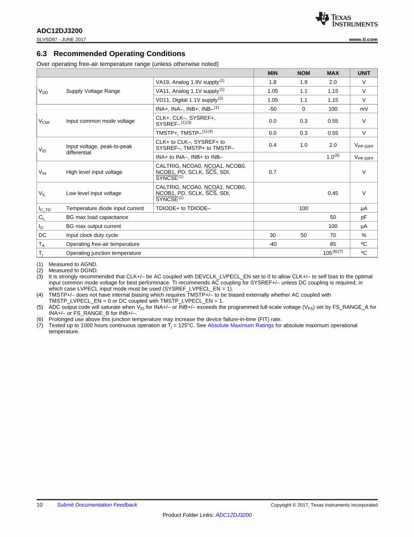
(1) Stresses beyond those listed under Absolute Maximum Ratings may cause permanent damage to the device. These are stress ratingsonly, which do not imply functional operation of the device at these or any other conditions beyond those indicated under RecommendedOperating Conditions. Exposure to absolute-maximum-rated conditions for extended periods may affect device reliability.
(2) Measured to AGND.(3) Measured to DGND.
6 Specifications
6.1 Absolute Maximum RatingsOver operating free-air temperature range (unless otherwise noted) (1)
MIN MAX UNIT
Supply Voltage Range
VA19 (2) -0.3 2.35 VVA11 (2) -0.3 1.32 VVD11 (3) -0.3 1.32 VVoltage between VD11 and VA11 -1.32 1.32 V
Voltage between AGND and DGND -0.1 0.1 V
Terminal Voltage Range
DA0...7+, DA0...7-, DB0...7+, DB0...7-,TMSTP+, TMSTP– (3) -0.5 min(1.32,
VD11+0.5) V
CLK+, CLK–, SYSREF+, SYSREF– (2) -0.5 min(1.32,VA11+0.5) V
BG, TDIODE+, TDIODE– (2) -0.5 min(2.35,VA19+0.5) V
INA+, INA–, INB+, INB– (2) -1 1 VCALSTAT, CALTRIG, NCOA0, NCOA1,NCOB0, NCOB1, ORA0, ORA1, ORB0,ORB1, PD, SCLK, SCS, SDI, SDO,SYNCSE (2)
-0.5 VA19+0.5 V
Peak input current (any input except INA+, INA–, INB+, INB–) -25 25 mAPeak input current (INA+, INA–, INB+, INB–) -50 50 mA
Peak RF input power (INA+, INA–, INB+, INB–) Single-ended with ZS-SE = 50 Ω or differentialwith ZS-DIFF = 100 Ω 16.4 dBm
Peak total input current (sum of absolute value of all currents forced in or out, not includingpower supply current) 100 mA
Operating junction temperature, Tj 150 °CStorage temperature, Tstg -65 150 °C
(1) JEDEC document JEP155 states that 500-V HBM allows safe manufacturing with a standard ESD control process.(2) JEDEC document JEP157 states that 250-V CDM allows safe manufacturing with a standard ESD control process.
6.2 ESD RatingsVALUE UNIT
V(ESD) Electrostatic dischargeHuman-body model (HBM), per ANSI/ESDA/JEDEC JS-001 (1) ± 2500
VCharged-device model (CDM), per JEDEC specification JESD22-C101 (2) ± 1000
10
ADC12DJ3200SLVSD97 –JUNE 2017 www.ti.com
Product Folder Links: ADC12DJ3200
Submit Documentation Feedback Copyright © 2017, Texas Instruments Incorporated
(1) Measured to AGND.(2) Measured to DGND.(3) It is strongly recommended that CLK+/– be AC coupled with DEVCLK_LVPECL_EN set to 0 to allow CLK+/– to self bias to the optimal
input common mode voltage for best performnace. TI recommends AC coupling for SYSREF+/– unless DC coupling is required, inwhich case LVPECL input mode must be used (SYSREF_LVPECL_EN = 1).
(4) TMSTP+/– does not have internal biasing which requires TMSTP+/– to be biased externally whether AC coupled withTMSTP_LVPECL_EN = 0 or DC coupled with TMSTP_LVPECL_EN = 1.
(5) ADC output code will saturate when VID for INA+/– or INB+/– exceeds the programmed full-scale voltage (VFS) set by FS_RANGE_A forINA+/– or FS_RANGE_B for INB+/–.
(6) Prolonged use above this junction temperature may increase the device failure-in-time (FIT) rate.(7) Tested up to 1000 hours continuous operation at Tj = 125°C. See Absolute Maximum Ratings for absolute maximum operational
temperature.
6.3 Recommended Operating ConditionsOver operating free-air temperature range (unless otherwise noted)
MIN NOM MAX UNIT
VDD Supply Voltage RangeVA19, Analog 1.9V supply (1) 1.8 1.9 2.0 VVA11, Analog 1.1V supply (1) 1.05 1.1 1.15 VVD11, Digital 1.1V supply (2) 1.05 1.1 1.15 V
VCMI Input common mode voltage
INA+, INA–, INB+, INB– (1) -50 0 100 mVCLK+, CLK–, SYSREF+,SYSREF– (1) (3) 0.0 0.3 0.55 V
TMSTP+, TMSTP– (1) (4) 0.0 0.3 0.55 V
VIDInput voltage, peak-to-peakdifferential
CLK+ to CLK–, SYSREF+ toSYSREF–, TMSTP+ to TMSTP– 0.4 1.0 2.0 VPP-DIFF
INA+ to INA–, INB+ to INB– 1.0 (5) VPP-DIFF
VIH High level input voltageCALTRIG, NCOA0, NCOA1, NCOB0,NCOB1, PD, SCLK, SCS, SDI,SYNCSE (1)
0.7 V
VIL Low level input voltageCALTRIG, NCOA0, NCOA1, NCOB0,NCOB1, PD, SCLK, SCS, SDI,SYNCSE (1)
0.45 V
IC_TD Temperature diode input current TDIODE+ to TDIODE– 100 µACL BG max load capacitance 50 pFIO BG max output current 100 µADC Input clock duty cycle 30 50 70 %TA Operating free-air temperature -40 85 ºCTj Operating junction temperature 105 (6) (7) ºC

11
ADC12DJ3200www.ti.com SLVSD97 –JUNE 2017
Product Folder Links: ADC12DJ3200
Submit Documentation FeedbackCopyright © 2017, Texas Instruments Incorporated
(1) For more information about traditional and new thermal metrics, see the Semiconductor and IC Package Thermal Metrics applicationreport.
NOTEPower down of the high speed data outputs (DA0+/– ... DA7+/–, DB0+/– ... DB7+/–) forextended times may reduce performance of the output serializers, especially at high datarates. Power down of the serializers occurs when the PD pin is held high, the MODEregister is programmed to a value other than 0x00 or 0x01, PD_ACH or PD_BCH registerssettings are programmed to 1 or when the JMODE register setting is programmed to amode that uses less than the 16 total lanes the device allows. For instance, JMODE 0uses eight total lanes and therefore the four highest indexed lanes for each JESD204Blink (DA4+/– ... DA7+/–, DB4+/– ... DB7+/–) are powered down in this mode. When the PDpin is held high or the MODE register is programmed to a value other than 0x00 or 0x01then all of the output serializers are powered down. When PD_ACH or PD_BCH registersettings are programmed to 1 the associated ADC channel and lanes are powered down.To prevent unreliable operation the PD pin and MODE register should only be used forbrief periods of time to measure temperature diode offsets and not used for long-termpower savings. Further, use of a JMODE that uses fewer than 16 lanes will result inunreliable operation of the unused lanes. If the system will never use the unused lanesduring the lifetime of the device then the unused lanes will not cause issues and can bepowered down. If the system may make use of the unused lanes at a later time, thereliable operation of the serializer outputs can be maintained by enabling JEXTRA_A andJEXTRA_B which results in VD11 power consumption to increase and the outputserializers to toggle.
6.4 Thermal Information
THERMAL METRIC (1)ADC12DJ3200
UNITAAV (FCBGA)144 PINS
RθJA Junction-to-ambient thermal resistance 25.3 °C/WRθJC(top) Junction-to-case (top) thermal resistance 1.1 °C/WRθJB Junction-to-board thermal resistance 8.2 °C/WψJT Junction-to-top characterization parameter 0.1 °C/WψJB Junction-to-board characterization parameter 8.2 °C/WRθJC(bot) Junction-to-case (bottom) thermal resistance n/a °C/W
12
ADC12DJ3200SLVSD97 –JUNE 2017 www.ti.com
Product Folder Links: ADC12DJ3200
Submit Documentation Feedback Copyright © 2017, Texas Instruments Incorporated
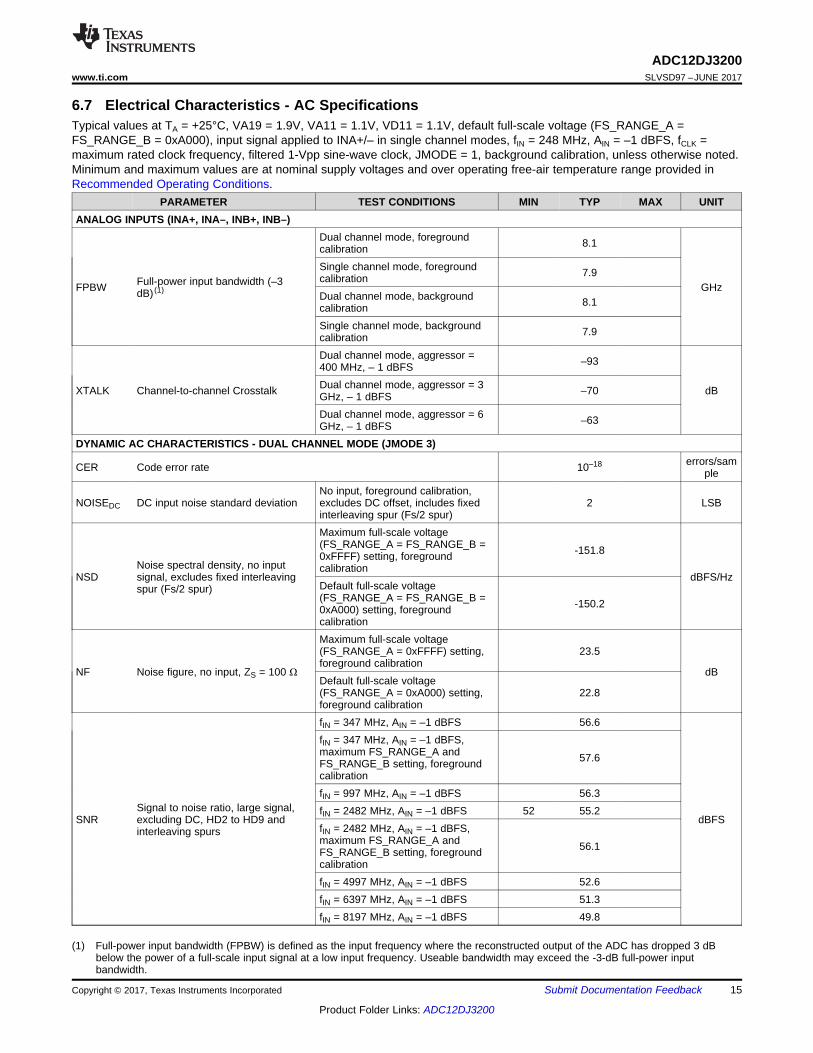
6.5 Electrical Characteristics - DC SpecificationsTypical values at TA = +25°C, VA19 = 1.9V, VA11 = 1.1V, VD11 = 1.1V, default full-scale voltage (FS_RANGE_A =FS_RANGE_B = 0xA000), input signal applied to INA+/– in single channel modes, fIN = 248 MHz, AIN = –1 dBFS, fCLK =maximum rated clock frequency, filtered 1-Vpp sine-wave clock, JMODE = 1, background calibration, unless otherwise noted.Minimum and maximum values are at nominal supply voltages and over operating free-air temperature range provided inRecommended Operating Conditions.
PARAMETER TEST CONDITIONS MIN TYP MAX UNITDC ACCURACYResolution Resolution with no missing codes 12 bitsDNL Differential nonlinearity ±0.3 LSBINL Integral nonlinearity ±2.5 LSBANALOG INPUTS (INA+, INA–, INB+, INB–)VOFF Offset Error Default full-scale voltage, OS_CAL disabled ±0.6 mV
VOFF_ADJInput offset voltageadjustment range
Available offset correction range (seeOS_CAL or OADJ_x_INx) ±55 mV
VOFF_DRIFT Offset DriftForeground calibration at nominaltemperature only 23 µV/°C
Foreground calibration at each temperature 0 µV/°C
VIN_FSRAnalog differential input fullscale range
Default full-scale voltage (FS_RANGE_A =FS_RANGE_B = 0xA000) 750 800 850 mVPP
Maximum full-scale voltage (FS_RANGE_A= FS_RANGE_B = 0xFFFF) 1000 1040 mVPP
Minimum full-scale voltage (FS_RANGE_A= FS_RANGE_B = 0x2000) 480 500 mVPP
VIN_FSR_DRIFTAnalog differential input fullscale range drift
Default FS_RANGE_A and FS_RANGE_Bsetting, foreground calibration at nominaltemperature only, inputs driven by 50-Ωsource, includes effect of RIN drift
-0.01 %/°C
Default FS_RANGE_A and FS_RANGE_Bsetting, foreground calibration at eachtemperature, inputs driven by 50-Ω source,includes effect of RIN drift
0.03 %/°C
VIN_FSR_MATCHAnalog differential input fullscale range matching
Matching between INA+/INA– andINB+/INB–, default setting, dual channelmode
0.625 %
RINSingle-ended input resistanceto AGND
Each input terminal is terminated to AGND,measured at TA = 25°C 48 50 52 Ω
RIN_TEMPCO Input termination linear temperature coefficient 17.6 mΩ/°C
CINSingle-ended inputcapacitance
Single channel mode at DC 0.4 pFDual channel mode at DC 0.4 pF
TEMPERATURE DIODE CHARACTERISTICS (TDIODE+, TDIODE–)
ΔVBETemperature diode voltageslope
Forced forward current of 100 µA. Offsetvoltage (approx. 0.792 V at 0°C) varies withprocess and must be measured for eachpart. Offset measurement should be donewith the device unpowered or with the PDpin asserted to minimize device self-heating.PD pin should be asserted only long enoughto take the offset measurement.
-1.6 mV/°C
BANDGAP VOLTAGE OUTPUT (BG)VBG Reference output voltage IL ≤ 100 µA 1.1 V
VBG_DRIFTReference output temperaturedrift IL ≤ 100 µA -64 µV/°C

13
ADC12DJ3200www.ti.com SLVSD97 –JUNE 2017
Product Folder Links: ADC12DJ3200
Submit Documentation FeedbackCopyright © 2017, Texas Instruments Incorporated
Electrical Characteristics - DC Specifications (continued)Typical values at TA = +25°C, VA19 = 1.9V, VA11 = 1.1V, VD11 = 1.1V, default full-scale voltage (FS_RANGE_A =FS_RANGE_B = 0xA000), input signal applied to INA+/– in single channel modes, fIN = 248 MHz, AIN = –1 dBFS, fCLK =maximum rated clock frequency, filtered 1-Vpp sine-wave clock, JMODE = 1, background calibration, unless otherwise noted.Minimum and maximum values are at nominal supply voltages and over operating free-air temperature range provided inRecommended Operating Conditions.
PARAMETER TEST CONDITIONS MIN TYP MAX UNITCLOCK INPUTS (CLK+, CLK–, SYSREF+, SYSREF–, TMSTP+, TMSTP–)
ZT Internal termination
Differential termination withDEVCLK_LVPECL_EN = 0,SYSREF_LVPECL_EN = 0 andTMSTP_LVPECL_EN = 0
110 Ω
Single ended termination to GND (per pin)with DEVCLK_LVPECL_EN = 0,SYSREF_LVPECL_EN = 0 andTMSTP_LVPECL_EN = 0
55 Ω
VCMInput common mode voltage,self-biased
Self-biasing common mode voltage forCLK+/– when AC coupled(DEVCLK_LVPECL_EN must be set to 0)
0.26 V
Self-biasing common mode voltage forSYSREF+/– when AC coupled(SYSREF_LVPECL_EN must be set to 0)and with receiver enabled(SYSREF_RECV_EN = 1).
0.29 V
Self-biasing common mode voltage forSYSREF+/– when AC coupled(SYSREF_LVPECL_EN must be set to 0)and with receiver disabled(SYSREF_RECV_EN = 0).
VA11 V
CL_DIFF Differential input capacitance Between positive and negative differentialinput pins 0.1 pF
CL_SESingle-ended inputcapacitance Each input to ground 0.5 pF
SERDES OUTPUTS (DA0+/DA0–...DA7+/DA7–, DB0+/DB0–...DB7+/DB7–)
VODDifferential output voltage,peak-to-peak 100-Ω load 550 600 650 mVPP-
DIFF
VCM Output common mode voltage AC coupled VD11/2 VZDIFF Differential output impedance 100 Ω
CMOS INTERFACE: SCLK, SDI, SDO, SCS, PD, NCOA0, NCOA1, NCOB0, NCOB1, CALSTAT, CALTRIG, ORA0, ORA1, ORB0, ORB1,SYNCSEIIH High level input current –40 40 µAIIL Low level input current –40 40 µACI Input capacitance 2 pFVOH High level output voltage ILOAD = –400 µA 1.65 VVOL Low level output voltage ILOAD = 400 µA 150 mV

14
ADC12DJ3200SLVSD97 –JUNE 2017 www.ti.com
Product Folder Links: ADC12DJ3200
Submit Documentation Feedback Copyright © 2017, Texas Instruments Incorporated
6.6 Electrical Characteristics - Power ConsumptionTypical values at TA = +25°C, VA19 = 1.9V, VA11 = 1.1V, VD11 = 1.1V, default full-scale voltage (FS_RANGE_A =FS_RANGE_B = 0xA000), input signal applied to INA+/– in single channel modes, fIN = 248 MHz, AIN = –1 dBFS, fCLK =maximum rated clock frequency, filtered 1-Vpp sine-wave clock, JMODE = 1, background calibration, unless otherwise noted.Minimum and maximum values are at nominal supply voltages and over operating free-air temperature range provided inRecommended Operating Conditions.
PARAMETER TEST CONDITIONS MIN TYP MAX UNITIVA19 1.9-V analog supply current
Power mode 1: Single channelmode, JMODE 1 (16 lanes, DDCbypassed), foreground calibration
897 mAIVA11 1.1-V analog supply current 491 mAIVD11 1.1-V digital supply current 640 mAPDIS Power dissipation 3.0 WIVA19 1.9-V analog supply current
Power mode 2: Single channelmode, JMODE 0 (8 lanes, DDCbypassed), foreground calibration
875 950 mAIVA11 1.1-V analog supply current 515 600 mAIVD11 1.1-V digital supply current 615 750 mAPDIS Power dissipation 2.9 3.5 WIVA19 1.9-V analog supply current
Power mode 3: Single channelmode, JMODE 1 (16 lanes, DDCbypassed), background calibration
1181 mAIVA11 1.1-V analog supply current 595 mAIVD11 1.1-V digital supply current 653 mAPDIS Power dissipation 3.6 WIVA19 1.9-V analog supply current
Power mode 4: Dual channel mode,JMODE 3 (16 lanes, DDCbypassed), background calibration
1260 mAIVA11 1.1-V analog supply current 594 mAIVD11 1.1-V digital supply current 636 mAPDIS Power dissipation 3.8 WIVA19 1.9-V analog supply current
Power mode 5: Dual channel mode,JMODE 11 (8 lanes, 4x decimation),foreground calibration
964 mAIVA11 1.1-V analog supply current 493 mAIVD11 1.1-V digital supply current 802 mAPDIS Power dissipation 3.3 W
15
ADC12DJ3200www.ti.com SLVSD97 –JUNE 2017
Product Folder Links: ADC12DJ3200
Submit Documentation FeedbackCopyright © 2017, Texas Instruments Incorporated
(1) Full-power input bandwidth (FPBW) is defined as the input frequency where the reconstructed output of the ADC has dropped 3 dBbelow the power of a full-scale input signal at a low input frequency. Useable bandwidth may exceed the -3-dB full-power inputbandwidth.
6.7 Electrical Characteristics - AC SpecificationsTypical values at TA = +25°C, VA19 = 1.9V, VA11 = 1.1V, VD11 = 1.1V, default full-scale voltage (FS_RANGE_A =FS_RANGE_B = 0xA000), input signal applied to INA+/– in single channel modes, fIN = 248 MHz, AIN = –1 dBFS, fCLK =maximum rated clock frequency, filtered 1-Vpp sine-wave clock, JMODE = 1, background calibration, unless otherwise noted.Minimum and maximum values are at nominal supply voltages and over operating free-air temperature range provided inRecommended Operating Conditions.
PARAMETER TEST CONDITIONS MIN TYP MAX UNITANALOG INPUTS (INA+, INA–, INB+, INB–)
FPBW Full-power input bandwidth (–3dB) (1)
Dual channel mode, foregroundcalibration 8.1
GHz
Single channel mode, foregroundcalibration 7.9
Dual channel mode, backgroundcalibration 8.1
Single channel mode, backgroundcalibration 7.9
XTALK Channel-to-channel Crosstalk
Dual channel mode, aggressor =400 MHz, – 1 dBFS –93
dBDual channel mode, aggressor = 3GHz, – 1 dBFS –70
Dual channel mode, aggressor = 6GHz, – 1 dBFS –63
DYNAMIC AC CHARACTERISTICS - DUAL CHANNEL MODE (JMODE 3)
CER Code error rate 10–18 errors/sample
NOISEDC DC input noise standard deviationNo input, foreground calibration,excludes DC offset, includes fixedinterleaving spur (Fs/2 spur)
2 LSB
NSDNoise spectral density, no inputsignal, excludes fixed interleavingspur (Fs/2 spur)
Maximum full-scale voltage(FS_RANGE_A = FS_RANGE_B =0xFFFF) setting, foregroundcalibration
-151.8
dBFS/HzDefault full-scale voltage(FS_RANGE_A = FS_RANGE_B =0xA000) setting, foregroundcalibration
-150.2
NF Noise figure, no input, ZS = 100 Ω
Maximum full-scale voltage(FS_RANGE_A = 0xFFFF) setting,foreground calibration
23.5
dBDefault full-scale voltage(FS_RANGE_A = 0xA000) setting,foreground calibration
22.8
SNRSignal to noise ratio, large signal,excluding DC, HD2 to HD9 andinterleaving spurs
fIN = 347 MHz, AIN = –1 dBFS 56.6
dBFS
fIN = 347 MHz, AIN = –1 dBFS,maximum FS_RANGE_A andFS_RANGE_B setting, foregroundcalibration
57.6
fIN = 997 MHz, AIN = –1 dBFS 56.3fIN = 2482 MHz, AIN = –1 dBFS 52 55.2fIN = 2482 MHz, AIN = –1 dBFS,maximum FS_RANGE_A andFS_RANGE_B setting, foregroundcalibration
56.1
fIN = 4997 MHz, AIN = –1 dBFS 52.6fIN = 6397 MHz, AIN = –1 dBFS 51.3fIN = 8197 MHz, AIN = –1 dBFS 49.8

16
ADC12DJ3200SLVSD97 –JUNE 2017 www.ti.com
Product Folder Links: ADC12DJ3200
Submit Documentation Feedback Copyright © 2017, Texas Instruments Incorporated
Electrical Characteristics - AC Specifications (continued)Typical values at TA = +25°C, VA19 = 1.9V, VA11 = 1.1V, VD11 = 1.1V, default full-scale voltage (FS_RANGE_A =FS_RANGE_B = 0xA000), input signal applied to INA+/– in single channel modes, fIN = 248 MHz, AIN = –1 dBFS, fCLK =maximum rated clock frequency, filtered 1-Vpp sine-wave clock, JMODE = 1, background calibration, unless otherwise noted.Minimum and maximum values are at nominal supply voltages and over operating free-air temperature range provided inRecommended Operating Conditions.
PARAMETER TEST CONDITIONS MIN TYP MAX UNIT
SNRSignal to noise ratio, small signal,excluding DC, HD2 to HD9 andinterleaving spurs
fIN = 347 MHz, AIN = –16 dBFS 57.4
dBFS
fIN = 997 MHz, AIN = –16 dBFS 57.5fIN = 2482 MHz, AIN = –16 dBFS 57.4fIN = 4997 MHz, AIN = –16 dBFS 57.1fIN = 6397 MHz, AIN = –16 dBFS 57.3fIN = 8197 MHz, AIN = –16 dBFS 56.9
SINADSignal to noise and distortion ratio,large signal, excluding DC and FS/2fixed spurs
fIN = 347 MHz, AIN = –1 dBFS 56.0
dBFS
fIN = 997 MHz, AIN = –1 dBFS 55.7fIN = 2482 MHz, AIN = –1 dBFS 51 54.6fIN = 4997 MHz, AIN = –1 dBFS 50.3fIN = 6397 MHz, AIN = –1 dBFS 48.9fIN = 8197 MHz, AIN = –1 dBFS 47.4
ENOBEffective number of bits, largesignal, excluding DC and FS/2 fixedspurs
fIN = 347 MHz, AIN = –1 dBFS 9.0
bits
fIN = 997 MHz, AIN = –1 dBFS 9.0fIN = 2482 MHz, AIN = –1 dBFS 8.2 8.8fIN = 4997 MHz, AIN = –1 dBFS 8.1fIN = 6397 MHz, AIN = –1 dBFS 7.8fIN = 8197 MHz, AIN = –1 dBFS 7.6
SFDRSpurious free dynamic range, largesignal, excluding DC and FS/2 fixedspurs
fIN = 347 MHz, AIN = –1 dBFS 67
dBFS
fIN = 347 MHz, AIN = –1 dBFS,maximum FS_RANGE_A andFS_RANGE_B setting, foregroundcalibration
67
fIN = 997 MHz, AIN = –1 dBFS 69fIN = 2482 MHz, AIN = –1 dBFS 60 66fIN = 2482 MHz, AIN = –1 dBFS,maximum FS_RANGE_A andFS_RANGE_B setting, foregroundcalibration
63
fIN = 4997 MHz, AIN = –1 dBFS 56fIN = 6397 MHz, AIN = –1 dBFS 55fIN = 8197 MHz, AIN = –1 dBFS 52
SFDRSpurious free dynamic range, smallsignal, excluding DC and FS/2 fixedspurs
fIN = 347 MHz, AIN = –16 dBFS 73
dBFS
fIN = 997 MHz, AIN = –16 dBFS 72fIN = 2482 MHz, AIN = –16 dBFS 72fIN = 4997 MHz, AIN = –16 dBFS 72fIN = 6397 MHz, AIN = –16 dBFS 72fIN = 8197 MHz, AIN = –16 dBFS 72
FS/2 FS/2 fixed interleaving spur,independent of input signal No input –75 –55 dBFS
17
ADC12DJ3200www.ti.com SLVSD97 –JUNE 2017
Product Folder Links: ADC12DJ3200
Submit Documentation FeedbackCopyright © 2017, Texas Instruments Incorporated
Electrical Characteristics - AC Specifications (continued)Typical values at TA = +25°C, VA19 = 1.9V, VA11 = 1.1V, VD11 = 1.1V, default full-scale voltage (FS_RANGE_A =FS_RANGE_B = 0xA000), input signal applied to INA+/– in single channel modes, fIN = 248 MHz, AIN = –1 dBFS, fCLK =maximum rated clock frequency, filtered 1-Vpp sine-wave clock, JMODE = 1, background calibration, unless otherwise noted.Minimum and maximum values are at nominal supply voltages and over operating free-air temperature range provided inRecommended Operating Conditions.
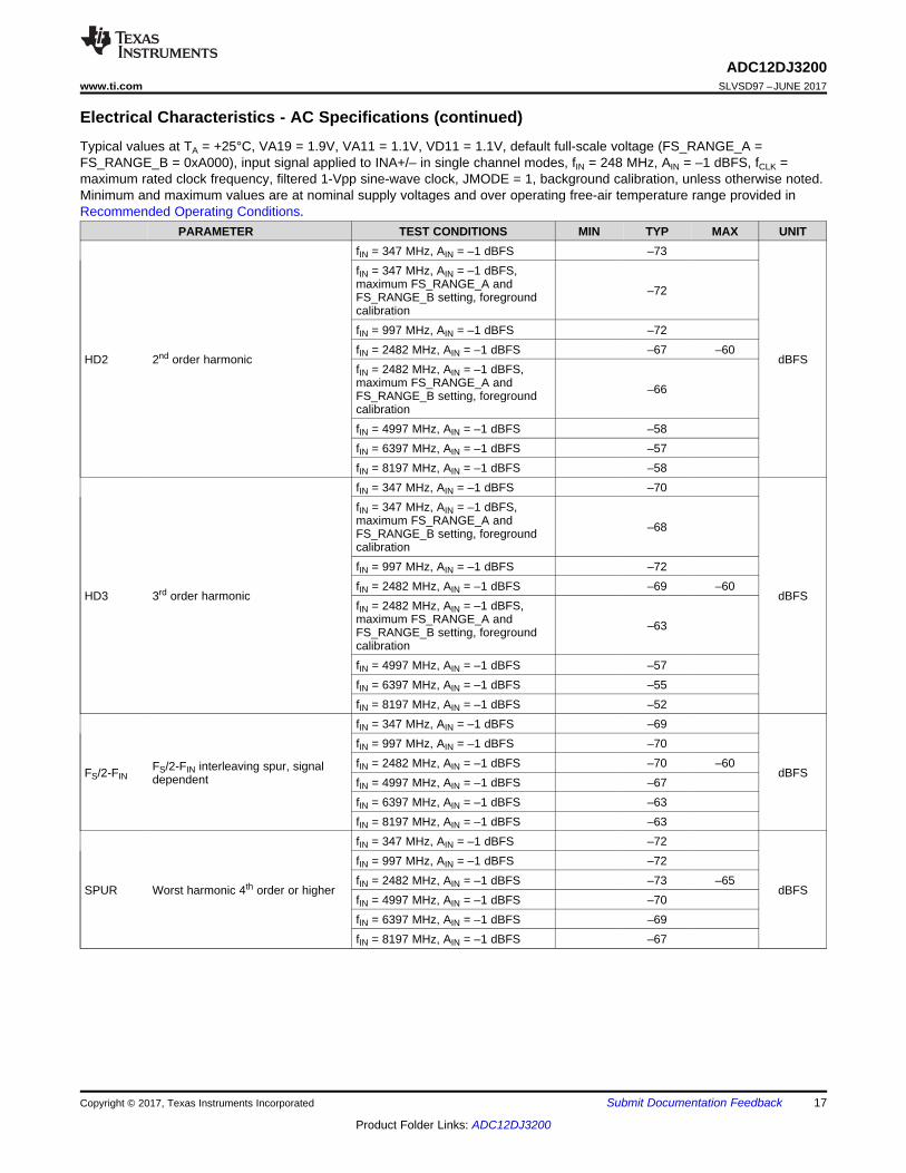
PARAMETER TEST CONDITIONS MIN TYP MAX UNIT
HD2 2nd order harmonic
fIN = 347 MHz, AIN = –1 dBFS –73
dBFS
fIN = 347 MHz, AIN = –1 dBFS,maximum FS_RANGE_A andFS_RANGE_B setting, foregroundcalibration
–72
fIN = 997 MHz, AIN = –1 dBFS –72fIN = 2482 MHz, AIN = –1 dBFS –67 –60fIN = 2482 MHz, AIN = –1 dBFS,maximum FS_RANGE_A andFS_RANGE_B setting, foregroundcalibration
–66
fIN = 4997 MHz, AIN = –1 dBFS –58fIN = 6397 MHz, AIN = –1 dBFS –57fIN = 8197 MHz, AIN = –1 dBFS –58
HD3 3rd order harmonic
fIN = 347 MHz, AIN = –1 dBFS –70
dBFS
fIN = 347 MHz, AIN = –1 dBFS,maximum FS_RANGE_A andFS_RANGE_B setting, foregroundcalibration
–68
fIN = 997 MHz, AIN = –1 dBFS –72fIN = 2482 MHz, AIN = –1 dBFS –69 –60fIN = 2482 MHz, AIN = –1 dBFS,maximum FS_RANGE_A andFS_RANGE_B setting, foregroundcalibration
–63
fIN = 4997 MHz, AIN = –1 dBFS –57fIN = 6397 MHz, AIN = –1 dBFS –55fIN = 8197 MHz, AIN = –1 dBFS –52
FS/2-FINFS/2-FIN interleaving spur, signaldependent
fIN = 347 MHz, AIN = –1 dBFS –69
dBFS
fIN = 997 MHz, AIN = –1 dBFS –70fIN = 2482 MHz, AIN = –1 dBFS –70 –60fIN = 4997 MHz, AIN = –1 dBFS –67fIN = 6397 MHz, AIN = –1 dBFS –63fIN = 8197 MHz, AIN = –1 dBFS –63
SPUR Worst harmonic 4th order or higher
fIN = 347 MHz, AIN = –1 dBFS –72
dBFS
fIN = 997 MHz, AIN = –1 dBFS –72fIN = 2482 MHz, AIN = –1 dBFS –73 –65fIN = 4997 MHz, AIN = –1 dBFS –70fIN = 6397 MHz, AIN = –1 dBFS –69fIN = 8197 MHz, AIN = –1 dBFS –67
18
ADC12DJ3200SLVSD97 –JUNE 2017 www.ti.com
Product Folder Links: ADC12DJ3200
Submit Documentation Feedback Copyright © 2017, Texas Instruments Incorporated
Electrical Characteristics - AC Specifications (continued)Typical values at TA = +25°C, VA19 = 1.9V, VA11 = 1.1V, VD11 = 1.1V, default full-scale voltage (FS_RANGE_A =FS_RANGE_B = 0xA000), input signal applied to INA+/– in single channel modes, fIN = 248 MHz, AIN = –1 dBFS, fCLK =maximum rated clock frequency, filtered 1-Vpp sine-wave clock, JMODE = 1, background calibration, unless otherwise noted.Minimum and maximum values are at nominal supply voltages and over operating free-air temperature range provided inRecommended Operating Conditions.
PARAMETER TEST CONDITIONS MIN TYP MAX UNIT
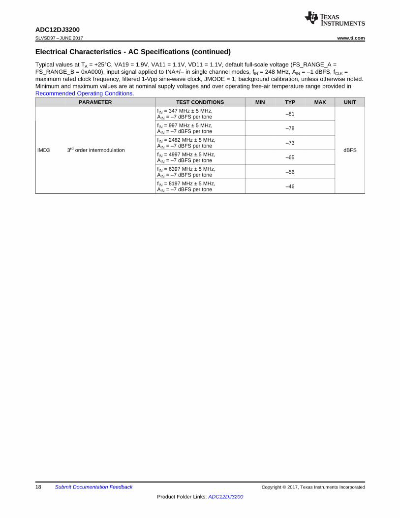
IMD3 3rd order intermodulation
fIN = 347 MHz ± 5 MHz,AIN = –7 dBFS per tone –81
dBFS
fIN = 997 MHz ± 5 MHz,AIN = –7 dBFS per tone –78
fIN = 2482 MHz ± 5 MHz,AIN = –7 dBFS per tone –73
fIN = 4997 MHz ± 5 MHz,AIN = –7 dBFS per tone –65
fIN = 6397 MHz ± 5 MHz,AIN = –7 dBFS per tone –56
fIN = 8197 MHz ± 5 MHz,AIN = –7 dBFS per tone –46
19
ADC12DJ3200www.ti.com SLVSD97 –JUNE 2017
Product Folder Links: ADC12DJ3200
Submit Documentation FeedbackCopyright © 2017, Texas Instruments Incorporated
Electrical Characteristics - AC Specifications (continued)Typical values at TA = +25°C, VA19 = 1.9V, VA11 = 1.1V, VD11 = 1.1V, default full-scale voltage (FS_RANGE_A =FS_RANGE_B = 0xA000), input signal applied to INA+/– in single channel modes, fIN = 248 MHz, AIN = –1 dBFS, fCLK =maximum rated clock frequency, filtered 1-Vpp sine-wave clock, JMODE = 1, background calibration, unless otherwise noted.Minimum and maximum values are at nominal supply voltages and over operating free-air temperature range provided inRecommended Operating Conditions.
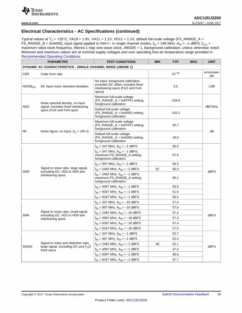
PARAMETER TEST CONDITIONS MIN TYP MAX UNITDYNAMIC AC CHARACTERISTICS - SINGLE CHANNEL MODE (JMODE 1)
CER Code error rate 10–18 errors/sample
NOISEDC DC input noise standard deviation
No input, foreground calibration,excludes DC offset, includes fixedinterleaving spurs (Fs/2 and Fs/4spurs)
3.5 LSB
NSDNoise spectral density, no inputsignal, excludes fixed interleavingspurs (Fs/2 and Fs/4 spur)
Maximum full-scale voltage(FS_RANGE_A = 0xFFFF) setting,foreground calibration
-154.6
dBFS/HzDefault full-scale voltage(FS_RANGE_A = 0xA000) setting,foreground calibration
-153.1
NF Noise figure, no input, ZS = 100 Ω
Maximum full-scale voltage(FS_RANGE_A = 0xFFFF) setting,foreground calibration
20.7
dBDefault full-scale voltage(FS_RANGE_A = 0xA000) setting,foreground calibration
19.9
SNRSignal to noise ratio, large signal,excluding DC, HD2 to HD9 andinterleaving spurs
fIN = 347 MHz, AIN = –1 dBFS 56.6
dBFS
fIN = 347 MHz, AIN = –1 dBFS,maximum FS_RANGE_A setting,foreground calibration
57.5
fIN = 997 MHz, AIN = –1 dBFS 56.3fIN = 2482 MHz, AIN = –1 dBFS 52 55.3fIN = 2482 MHz, AIN = –1 dBFS,maximum FS_RANGE_A setting,foreground calibration
56.1
fIN = 4997 MHz, AIN = –1 dBFS 53.0fIN = 6397 MHz, AIN = –1 dBFS 51.6fIN = 8197 MHz, AIN = –1 dBFS 50.0
SNRSignal to noise ratio, small signal,excluding DC, HD2 to HD9 andinterleaving spurs
fIN = 347 MHz, AIN = –16 dBFS 57.4
dBFS
fIN = 997 MHz, AIN = –16 dBFS 57.6fIN = 2482 MHz, AIN = –16 dBFS 57.4fIN = 4997 MHz, AIN = –16 dBFS 57.3fIN = 6397 MHz, AIN = –16 dBFS 57.4fIN = 8197 MHz, AIN = –16 dBFS 57.0
SINADSignal to noise and distortion ratio,large signal, excluding DC and FS/2fixed spurs
fIN = 347 MHz, AIN = –1 dBFS 52.7
dBFS
fIN = 997 MHz, AIN = –1 dBFS 52.4fIN = 2482 MHz, AIN = –1 dBFS 48 52.1fIN = 4997 MHz, AIN = –1 dBFS 47.5fIN = 6397 MHz, AIN = –1 dBFS 46.6fIN = 8197 MHz, AIN = –1 dBFS 47.7

20
ADC12DJ3200SLVSD97 –JUNE 2017 www.ti.com
Product Folder Links: ADC12DJ3200
Submit Documentation Feedback Copyright © 2017, Texas Instruments Incorporated
Electrical Characteristics - AC Specifications (continued)Typical values at TA = +25°C, VA19 = 1.9V, VA11 = 1.1V, VD11 = 1.1V, default full-scale voltage (FS_RANGE_A =FS_RANGE_B = 0xA000), input signal applied to INA+/– in single channel modes, fIN = 248 MHz, AIN = –1 dBFS, fCLK =maximum rated clock frequency, filtered 1-Vpp sine-wave clock, JMODE = 1, background calibration, unless otherwise noted.Minimum and maximum values are at nominal supply voltages and over operating free-air temperature range provided inRecommended Operating Conditions.
PARAMETER TEST CONDITIONS MIN TYP MAX UNIT
ENOBEffective number of bits, largesignal, excluding DC and FS/2 fixedspurs
fIN = 347 MHz, AIN = –1 dBFS 8.6
dBFS
fIN = 997 MHz, AIN = –1 dBFS 8.5fIN = 2482 MHz, AIN = –1 dBFS 7.7 8.4fIN = 4997 MHz, AIN = –1 dBFS 7.7fIN = 6397 MHz, AIN = –1 dBFS 7.5fIN = 8197 MHz, AIN = –1 dBFS 7.6
SFDRSpurious free dynamic range, largesignal, excluding DC, FS/4 and FS/2fixed spurs
fIN = 347 MHz, AIN = –1 dBFS 67
dBFS
fIN = 347 MHz, AIN = –1 dBFS,maximum FS_RANGE_A setting,foreground calibration
64
fIN = 997 MHz, AIN = –1 dBFS 63fIN = 2482 MHz, AIN = –1 dBFS 50 58fIN = 2482 MHz, AIN = –1 dBFS,maximum FS_RANGE_A setting,foreground calibration
55
fIN = 4997 MHz, AIN = –1 dBFS 51fIN = 6397 MHz, AIN = –1 dBFS 50fIN = 8197 MHz, AIN = –1 dBFS 48
SFDRSpurious free dynamic range, smallsignal, excluding DC, FS/4 and FS/2fixed spurs
fIN = 347 MHz, AIN = –16 dBFS 75
dBFS
fIN = 997 MHz, AIN = –16 dBFS 73fIN = 2482 MHz, AIN = –16 dBFS 72fIN = 4997 MHz, AIN = –16 dBFS 66fIN = 6397 MHz, AIN = –16 dBFS 65fIN = 8197 MHz, AIN = –16 dBFS 63
FS/2 FS/2 fixed interleaving spur,independent of input signal
No input, OS_CAL disabled. Spurcan be improved by runningOS_CAL.
–56 dBFS
FS/4 FS/4 fixed interleaving spur,independent of input signal No input –65 –55 dBFS
HD2 2nd order harmonic
fIN = 347 MHz, AIN = –1 dBFS –73
dBFS
fIN = 347 MHz, AIN = –1 dBFS,maximum FS_RANGE_A setting,foreground calibration
–76
fIN = 997 MHz, AIN = –1 dBFS –74fIN = 2482 MHz, AIN = –1 dBFS –68 –60fIN = 2482 MHz, AIN = –1 dBFS,maximum FS_RANGE_A setting,foreground calibration
–72
fIN = 4997 MHz, AIN = –1 dBFS –62fIN = 6397 MHz, AIN = –1 dBFS –62fIN = 8197 MHz, AIN = –1 dBFS –61

21
ADC12DJ3200www.ti.com SLVSD97 –JUNE 2017
Product Folder Links: ADC12DJ3200
Submit Documentation FeedbackCopyright © 2017, Texas Instruments Incorporated
Electrical Characteristics - AC Specifications (continued)Typical values at TA = +25°C, VA19 = 1.9V, VA11 = 1.1V, VD11 = 1.1V, default full-scale voltage (FS_RANGE_A =FS_RANGE_B = 0xA000), input signal applied to INA+/– in single channel modes, fIN = 248 MHz, AIN = –1 dBFS, fCLK =maximum rated clock frequency, filtered 1-Vpp sine-wave clock, JMODE = 1, background calibration, unless otherwise noted.Minimum and maximum values are at nominal supply voltages and over operating free-air temperature range provided inRecommended Operating Conditions.
PARAMETER TEST CONDITIONS MIN TYP MAX UNIT
HD3 3rd order harmonic
fIN = 347 MHz, AIN = –1 dBFS –70
dBFS
fIN = 347 MHz, AIN = –1 dBFS,maximum FS_RANGE_A setting,foreground calibration
–68
fIN = 997 MHz, AIN = –1 dBFS –68fIN = 2482 MHz, AIN = –1 dBFS –69 –60fIN = 2482 MHz, AIN = –1 dBFS,maximum FS_RANGE_A setting,foreground calibration
–64
fIN = 4997 MHz, AIN = –1 dBFS –59fIN = 6397 MHz, AIN = –1 dBFS –58fIN = 8197 MHz, AIN = –1 dBFS –55
FS/2-FINFS/2-FIN interleaving spur, signaldependent
fIN = 347 MHz, AIN = –1 dBFS –68
dBFS
fIN = 997 MHz, AIN = –1 dBFS –63fIN = 2482 MHz, AIN = –1 dBFS –58 –50fIN = 4997 MHz, AIN = –1 dBFS –51fIN = 6397 MHz, AIN = –1 dBFS –50fIN = 8197 MHz, AIN = –1 dBFS –48
FS/4±FINFS/4±FIN interleaving spurs, signaldependent
fIN = 347 MHz, AIN = –1 dBFS –74
dBFS
fIN = 997 MHz, AIN = –1 dBFS –69fIN = 2482 MHz, AIN = –1 dBFS –70 –60fIN = 4997 MHz, AIN = –1 dBFS –66fIN = 6397 MHz, AIN = –1 dBFS –63fIN = 8197 MHz, AIN = –1 dBFS –61
SPUR Worst harmonic 4th order or higher
fIN = 347 MHz, AIN = –1 dBFS –73
dBFS
fIN = 997 MHz, AIN = –1 dBFS –73fIN = 2482 MHz, AIN = –1 dBFS –75 –65fIN = 4997 MHz, AIN = –1 dBFS –69fIN = 6397 MHz, AIN = –1 dBFS –69fIN = 8197 MHz, AIN = –1 dBFS –63
IMD3 3rd order intermodulation
fIN = 347 MHz ± 5 MHz,AIN = –7 dBFS per tone –80
dBFS
fIN = 997 MHz ± 5 MHz,AIN = –7 dBFS per tone –75
fIN = 2482 MHz ± 5 MHz,AIN = –7 dBFS per tone –72
fIN = 4997 MHz ± 5 MHz,AIN = –7 dBFS per tone –63
fIN = 6397 MHz ± 5 MHz,AIN = –7 dBFS per tone –65
fIN = 8197 MHz ± 5 MHz,AIN = –7 dBFS per tone –50

22
ADC12DJ3200SLVSD97 –JUNE 2017 www.ti.com
Product Folder Links: ADC12DJ3200
Submit Documentation Feedback Copyright © 2017, Texas Instruments Incorporated
(1) Unless functionally limited to a smaller range in Table 18 based on programmed JMODE.(2) SYSREF_POS should be used to select an optimal SYSREF_SEL value for SYSREF capture, see SYSREF Position Detector and
Sampling Position Selection (SYSREF Windowing) for more information on SYSREF Windowing. The invalid region, specified bytINV(SYSREF), indicates the portion of the CLK+/– period (tCLK), as measured by SYSREF_SEL, that may result in a setup and holdviolation. The user should verify that the timing skew between SYSREF+/– and CLK+/– over system operating conditions from thenominal conditions (that used to find optimal SYSREF_SEL) does not result in the invalid region occurring at the selected SYSREF_SELposition in SYSREF_POS, otherwise a temperature dependent SYSREF_SEL selection may be needed to track the skew betweenCLK+/– and SYSREF+/–.
6.8 Timing RequirementsMIN NOM MAX UNIT
DEVICE (SAMPLING) CLOCK (CLK+, CLK–)
fCLKInput clock frequency (CLK+, CLK–), both single channel and dual channelmodes (1) 800 3200 MHz
SYSREF (SYSREF+, SYSREF–)
tINV(SYSREF)Width of invalid SYSREF capture region of CLK+/– period, indicating setupor hold time violation, as measured by SYSREF_POS status register (2) 48 ps
tINV(TEMP)Drift of invalid SYSREF capture region over temperature, positive numberindicates a shift toward MSB of SYSREF_POS register 0 ps/°C
tINV(VA11)Drift of invalid SYSREF capture region over VA11 supply voltage, positivenumber indicates a shift toward MSB of SYSREF_POS register 0.36 ps/mV
tSTEP(SP) Delay of SYSREF_POS LSBSYSREF_ZOOM = 0 77 psSYSREF_ZOOM = 1 24 ps
t(PH_SYS)Minimum SYSREF+/– assertion duration after SYSREF+/– rising edgeevent 4 ns
t(PL_SYS)Minimum SYSREF+/– deassertion duration after SYSREF+/– falling edgeevent 1 ns
JESD204B SYNC TIMING (SYNCSE OR TMSTP+/–)
tH(SYNCSE)
Minimum hold time from multi-frame boundary(SYSREF rising edge captured high) to de-assertion of JESD204B SYNC signal (SYNCSE ifSYNC_SEL = 0 or TMSTP+/– if SYNC_SEL = 1)for NCO synchronization (NCO_SYNC_ILA = 1)
JMODE = 0, 2, 4, 6,10, 13 or 15 21
tCLKcyclesJMODE = 1, 3, 5, 7, 9,
11, 14 or 16 17
JMODE = 12, 17 or 18 9
tSU(SYNCSE)
Minimum setup time from de-assertion ofJESD204B SYNC signal (SYNCSE if SYNC_SEL= 0 or TMSTP+/– if SYNC_SEL = 1) to multi-frame boundary (SYSREF rising edge capturedhigh) for NCO synchronization (NCO_SYNC_ILA= 1)
JMODE = 0, 2, 4, 6,10, 13 or 15 –2
tCLKcyclesJMODE = 1, 3, 5, 7, 9,
11, 14 or 16 2
JMODE = 12, 17 or 18 10
t(SYNCSE) SYNCSE minimum assertion time to trigger link resynchronization 4 FramesSERIAL PROGRAMMING INTERFACE (SCLK, SDI, SCS)fCLK(SCLK) Maximum serial clock frequency 15.625 MHzt(PH) Minimum serial clock high value pulse width 32 nst(PL) Minimum serial clock low value pulse width 32 ns
tSU(SCS)Minimum setup time from SCS to rising edge ofSCLK 30 ns
tH(SCS)Minimum hold time from rising edge of SCLK toSCS 3 ns
tSU(SDI)Minimum setup time from SDI to rising edge ofSCLK 30 ns
tH(SDI)Minimum hold time from rising edge of SCLK toSDI 3 ns
23
ADC12DJ3200www.ti.com SLVSD97 –JUNE 2017
Product Folder Links: ADC12DJ3200
Submit Documentation FeedbackCopyright © 2017, Texas Instruments Incorporated
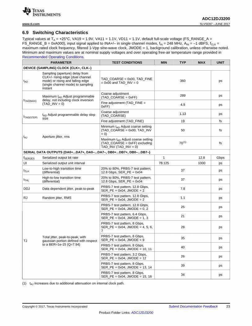
(1) tAJ increases due to additional attenuation on internal clock path.
6.9 Switching CharacteristicsTypical values at TA = +25°C, VA19 = 1.9V, VA11 = 1.1V, VD11 = 1.1V, default full-scale voltage (FS_RANGE_A =FS_RANGE_B = 0xA000), input signal applied to INA+/– in single channel modes, fIN = 248 MHz, AIN = –1 dBFS, fCLK =maximum rated clock frequency, filtered 1-Vpp sine-wave clock, JMODE = 1, background calibration, unless otherwise noted.Minimum and maximum values are at nominal supply voltages and over operating free-air temperature range provided inRecommended Operating Conditions.
PARAMETER TEST CONDITIONS MIN TYP MAX UNITDEVICE (SAMPLING) CLOCK (CLK+, CLK–)
tAD
Sampling (aperture) delay fromCLK+/- rising edge (dual channelmode) or rising and falling edge(single channel mode) to samplinginstant
TAD_COARSE = 0x00, TAD_FINE= 0x00 and TAD_INV = 0 360 ps
tTAD(MAX)
Maximum tAD Adjust programmabledelay, not including clock inversion(TAD_INV = 0)
Coarse adjustment(TAD_COARSE = 0xFF) 289 ps
Fine adjustment (TAD_FINE =0xFF) 4.9 ps
tTAD(STEP)tAD Adjust programmable delay stepsize
Coarse adjustment(TAD_COARSE) 1.13 ps
Fine adjustment (TAD_FINE) 19 fs
tAJ Aperture jitter, rms
Minimum tAD Adjust coarse setting(TAD_COARSE = 0x00, TAD_INV= 0)
50 fs
Maximum tAD Adjust coarse setting(TAD_COARSE = 0xFF) excludingTAD_INV (TAD_INV = 0)
70 (1) fs
SERIAL DATA OUTPUTS (DA0+...DA7+, DA0–...DA7–, DB0+...DB7+, DB0–...DB7–)fSERDES Serialized output bit rate 1 12.8 GbpsUI Serialized output unit interval 78.125 1000 ps
tTLHLow-to-high transition time(differential)
20% to 80%, PRBS-7 test pattern,12.8 Gbps, SER_PE = 0x04 37 ps
tTHLHigh-to-low transition time(differential)
20% to 80%, PRBS-7 test pattern,12.8 Gbps, SER_PE = 0x04 37 ps
DDJ Data dependent jitter, peak-to-peak PRBS-7 test pattern, 12.8 Gbps,SER_PE = 0x04, JMODE = 2 7.8 ps
RJ Random jitter, RMS PRBS-7 test pattern, 12.8 Gbps,SER_PE = 0x04, JMODE = 2 1.1 ps
TJTotal jitter, peak-to-peak, withgaussian portion defined with respectto a BER=1e-15 (Q=7.94)
PRBS-7 test pattern, 12.8 Gbps,SER_PE = 0x04, JMODE = 0, 2 25 ps
PRBS-7 test pattern, 6.4 Gbps,SER_PE = 0x04, JMODE = 1, 3 21 ps
PRBS-7 test pattern, 8 Gbps,SER_PE = 0x04, JMODE = 4, 5, 6,7
28 ps
PRBS-7 test pattern, 8 Gbps,SER_PE = 0x04, JMODE = 9 35 ps
PRBS-7 test pattern, 8 Gbps,SER_PE = 0x04, JMODE = 10, 11 40 ps
PRBS-7 test pattern, 3.2 Gbps,SER_PE = 0x04, JMODE = 12 26 ps
PRBS-7 test pattern, 8 Gbps,SER_PE = 0x04, JMODE = 13, 14 39 ps
PRBS-7 test pattern, 8 Gbps,SER_PE = 0x04, JMODE = 15, 16 34 ps

24
ADC12DJ3200SLVSD97 –JUNE 2017 www.ti.com
Product Folder Links: ADC12DJ3200
Submit Documentation Feedback Copyright © 2017, Texas Instruments Incorporated
Switching Characteristics (continued)Typical values at TA = +25°C, VA19 = 1.9V, VA11 = 1.1V, VD11 = 1.1V, default full-scale voltage (FS_RANGE_A =FS_RANGE_B = 0xA000), input signal applied to INA+/– in single channel modes, fIN = 248 MHz, AIN = –1 dBFS, fCLK =maximum rated clock frequency, filtered 1-Vpp sine-wave clock, JMODE = 1, background calibration, unless otherwise noted.Minimum and maximum values are at nominal supply voltages and over operating free-air temperature range provided inRecommended Operating Conditions.
PARAMETER TEST CONDITIONS MIN TYP MAX UNIT
(2) tADC is an exact, unrounded, deterministic delay. The delay can be negative if the reference sample is sampled after the SYSREF highcapture point, in which case the total latency is smaller than the delay given by tTX.
(3) The values given for tTX include deterministic and non-deterministic delays. Over process, temperature, and voltage, the delay will vary.JESD204B accounts for these variations when operating in subclass-1 mode in order to achieve deterministic latency. Proper receiverRBD value must be chosen such that the elastic buffer release point does not occur within the invalid region of the local multi-frameclock (LMFC) cycle.
ADC CORE LATENCY
tADC
Deterministic delay from the CLK+/–edge that samples the referencesample to the CLK+/– edge thatsamples SYSREF going high (2)
JMODE = 0 -8.5
tCLK cycles
JMODE = 1 -20.5JMODE = 2 -9JMODE = 3 -21JMODE = 4 -4.5JMODE = 5 -24.5JMODE = 6 -5JMODE = 7 -25JMODE = 9 60JMODE = 10 140JMODE = 11 136JMODE = 12 120JMODE = 13 232JMODE = 14 232JMODE = 15 446JMODE = 16 430JMODE = 17 -48.5JMODE = 18 -49
JESD204B AND SERIALIZER LATENCY
tTX
Delay from the CLK+/– rising edgethat samples SYSREF high to the firstbit of the multi-frame on theJESD204B serial output lanecorresponding to the referencesample of tADC
(3)
JMODE = 0 72 84
tCLK cycles
JMODE = 1 119 132JMODE = 2 72 84JMODE = 3 119 132JMODE = 4 67 80JMODE = 5 106 119JMODE = 6 67 80JMODE = 7 106 119JMODE = 9 106 119JMODE = 10 67 80JMODE = 11 106 119JMODE = 12 213 225JMODE = 13 67 80JMODE = 14 106 119JMODE = 15 67 80JMODE = 16 106 119JMODE = 17 195 208JMODE = 18 195 208
CLK+
CLK±
DA0+/±(2)
SYSREF+
SYSREF±
/R
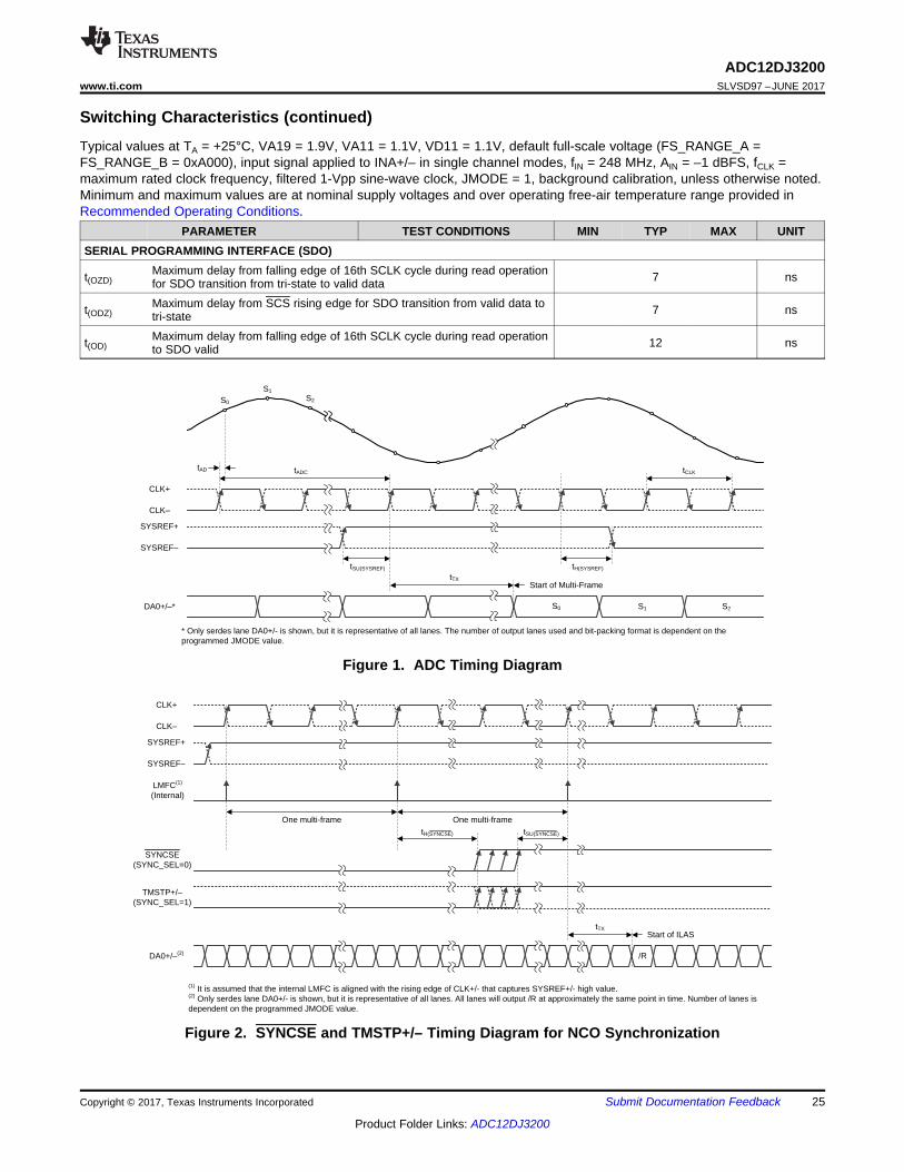
(1) It is assumed that the internal LMFC is aligned with the rising edge of CLK+/- that captures SYSREF+/- high value.(2) Only serdes lane DA0+/- is shown, but it is representative of all lanes. All lanes will output /R at approximately the same point in time. Number of lanes is dependent on the programmed JMODE value.
SYNCSE(SYNC_SEL=0)
tH(SYNCSE) tSU(SYNCSE)
tTXStart of ILAS
LMFC(1)
(Internal)
One multi-frame One multi-frame
TMSTP+/±(SYNC_SEL=1)
CLK+
CLK±
DA0+/±*
tAD tADC
SYSREF+
SYSREF±
tSU(SYSREF)
tTX
S0
S1
S2
tCLK
S0 S1 S2
* Only serdes lane DA0+/- is shown, but it is representative of all lanes. The number of output lanes used and bit-packing format is dependent on the programmed JMODE value.
tH(SYSREF)
Start of Multi-Frame
25
ADC12DJ3200www.ti.com SLVSD97 –JUNE 2017
Product Folder Links: ADC12DJ3200
Submit Documentation FeedbackCopyright © 2017, Texas Instruments Incorporated
Switching Characteristics (continued)Typical values at TA = +25°C, VA19 = 1.9V, VA11 = 1.1V, VD11 = 1.1V, default full-scale voltage (FS_RANGE_A =FS_RANGE_B = 0xA000), input signal applied to INA+/– in single channel modes, fIN = 248 MHz, AIN = –1 dBFS, fCLK =maximum rated clock frequency, filtered 1-Vpp sine-wave clock, JMODE = 1, background calibration, unless otherwise noted.Minimum and maximum values are at nominal supply voltages and over operating free-air temperature range provided inRecommended Operating Conditions.
PARAMETER TEST CONDITIONS MIN TYP MAX UNITSERIAL PROGRAMMING INTERFACE (SDO)
t(OZD)Maximum delay from falling edge of 16th SCLK cycle during read operationfor SDO transition from tri-state to valid data 7 ns
t(ODZ)Maximum delay from SCS rising edge for SDO transition from valid data totri-state 7 ns
t(OD)Maximum delay from falling edge of 16th SCLK cycle during read operationto SDO valid 12 ns
Figure 1. ADC Timing Diagram
Figure 2. SYNCSE and TMSTP+/– Timing Diagram for NCO Synchronization

tH(SCS)
1st
clock
SCLK
16th
clock 24th
clock
SCS
tSU(SCS)
t(ODZ)
SDI
t(OZD)
D7 D0D1
COMMAND FIELDt(OD)
D7 D0D1SDO
Write Command
Read Command
tSU(SDI) tH(SDI)
t(PH) t(PL)
t(PH) + t(PL) = t(P) = 1 / ¦CLK(SCLK)
Hi-Z Hi-Z
tH(SCS)tSU(SCS)
tSU(SDI) tH(SDI)
26
ADC12DJ3200SLVSD97 –JUNE 2017 www.ti.com
Product Folder Links: ADC12DJ3200
Submit Documentation Feedback Copyright © 2017, Texas Instruments Incorporated
Figure 3. Serial Interface Timing
Fin (MHz)
Mag
nitu
de (
dBF
S)
0 2000 4000 6000 8000 10000-85
-80
-75
-70
-65
-60
-55
-50
D130
H2 (dBFS)H3 (dBFS)THD (dBFS)
Fclk (MHz)
Pow
er C
onsu
mpt
ion
(W)
800 1200 1600 2000 2400 2800 32002
2.2
2.4
2.6
2.8
3
3.2
D008
Fin (MHz)
EN
OB
(B
its)
0 2000 4000 6000 8000 100007
7.25
7.5
7.75
8
8.25
8.5
8.75
9
D002
BG CalibrationFG Calibration
Fin (MHz)
Mag
nitu
de (
dBF
S)
0 2000 4000 6000 8000 1000040
45
50
55
60
65
70
75
D129
SNR (dBFS)SINAD (dBFS)SFDR (dBFS)
Fin (MHz)
EN
OB
(B
its)
0 2000 4000 6000 8000 100007.25
7.5
7.75
8
8.25
8.5
8.75
9
9.25
D132Fin (MHz)
Mag
nitu
de (
dBF
S)
0 2000 4000 6000 8000 1000040
45
50
55
60
65
70
75
D131
SNR (dBFS)SINAD (dBFS)SFDR (dBFS)
27
ADC12DJ3200www.ti.com SLVSD97 –JUNE 2017
Product Folder Links: ADC12DJ3200
Submit Documentation FeedbackCopyright © 2017, Texas Instruments Incorporated
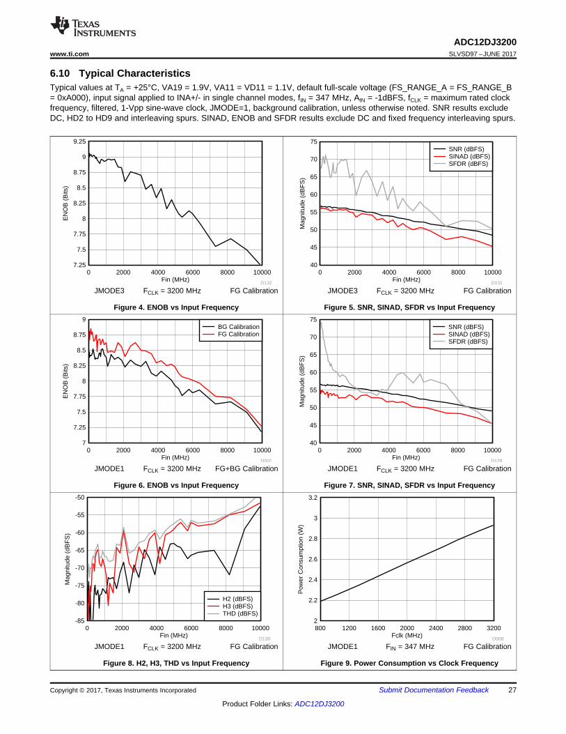
6.10 Typical CharacteristicsTypical values at TA = +25°C, VA19 = 1.9V, VA11 = VD11 = 1.1V, default full-scale voltage (FS_RANGE_A = FS_RANGE_B= 0xA000), input signal applied to INA+/- in single channel modes, fIN = 347 MHz, AIN = -1dBFS, fCLK = maximum rated clockfrequency, filtered, 1-Vpp sine-wave clock, JMODE=1, background calibration, unless otherwise noted. SNR results excludeDC, HD2 to HD9 and interleaving spurs. SINAD, ENOB and SFDR results exclude DC and fixed frequency interleaving spurs.
JMODE3 FCLK = 3200 MHz FG Calibration
Figure 4. ENOB vs Input Frequency
JMODE3 FCLK = 3200 MHz FG Calibration
Figure 5. SNR, SINAD, SFDR vs Input Frequency
JMODE1 FCLK = 3200 MHz FG+BG Calibration
Figure 6. ENOB vs Input Frequency
JMODE1 FCLK = 3200 MHz FG Calibration
Figure 7. SNR, SINAD, SFDR vs Input Frequency
JMODE1 FCLK = 3200 MHz FG Calibration
Figure 8. H2, H3, THD vs Input Frequency
JMODE1 FIN = 347 MHz FG Calibration
Figure 9. Power Consumption vs Clock Frequency

Ambient Temperature (°C)
Mag
nitu
de (
dBF
S)
-75 -50 -25 0 25 50 75 100 125-90
-85
-80
-75
-70
-65
-60
-55
D119
FG Calibration Each TemperatureFG Calibration at 25°C
Ambient Temperature (°C)
Mag
nitu
de (
dBF
S)
-75 -50 -25 0 25 50 75 100 125-90
-85
-80
-75
-70
-65
-60
-55
D120
FG Calibration Each TemperatureFG Calibration at 25°C
Ambient Temperature (°C)
Mag
nitu
de (
dBF
S)
-75 -50 -25 0 25 50 75 100 12548
50
52
54
56
58
60
D063
FG Calibration Each TemperatureFG Calibration at 25°C
Ambient Temperature (°C)
Mag
nitu
de (
dBF
S)
-75 -50 -25 0 25 50 75 100 12552
56
60
64
68
72
D064
FG Calibration Each TemperatureFG Calibration at 25°C
Ambient Temperature (°C)
EN
OB
(B
its)
-75 -50 -25 0 25 50 75 100 1258
8.25
8.5
8.75
9
D040
BG CalibrationFG Calibration Each Temperature
Ambient Temperature (°C)
EN
OB
(B
its)
-75 -50 -25 0 25 50 75 100 1257
7.5
8
8.5
9
D121
FG Calibration Each TemperatureFG Calibration at 25°C
28
ADC12DJ3200SLVSD97 –JUNE 2017 www.ti.com
Product Folder Links: ADC12DJ3200
Submit Documentation Feedback Copyright © 2017, Texas Instruments Incorporated
Typical Characteristics (continued)Typical values at TA = +25°C, VA19 = 1.9V, VA11 = VD11 = 1.1V, default full-scale voltage (FS_RANGE_A = FS_RANGE_B= 0xA000), input signal applied to INA+/- in single channel modes, fIN = 347 MHz, AIN = -1dBFS, fCLK = maximum rated clockfrequency, filtered, 1-Vpp sine-wave clock, JMODE=1, background calibration, unless otherwise noted. SNR results excludeDC, HD2 to HD9 and interleaving spurs. SINAD, ENOB and SFDR results exclude DC and fixed frequency interleaving spurs.
JMODE1 FIN = 2400 MHz
Figure 10. ENOB vs Temperature
JMODE1 FIN = 600 MHz FCLK = 3200 MHz
Figure 11. ENOB vs Temperature and Calibration Type
JMODE1 FIN = 600 MHz FCLK = 3200 MHz
Figure 12. SNR vs Temperature and Calibration Type
JMODE1 FIN = 600 MHz FCLK = 3200 MHz
Figure 13. SFDR vs Temperature and Calibration Type
JMODE1 FIN = 600 MHz FCLK = 3200 MHz
Figure 14. H2 vs Temperature and Calibration Type
JMODE1 FIN = 600 MHz FCLK = 3200 MHz
Figure 15. H3 vs Temperature and Calibration Type
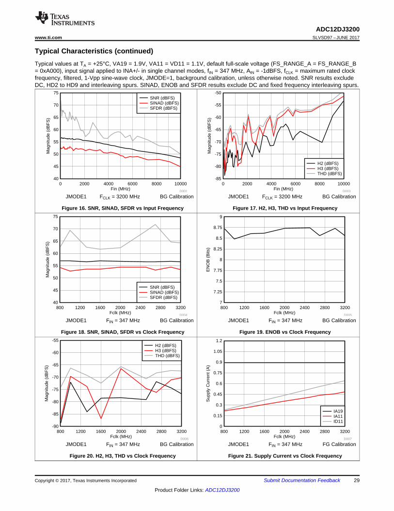
Fclk (MHz)
Mag
nitu
de (
dBF
S)
800 1200 1600 2000 2400 2800 3200-90
-85
-80
-75
-70
-65
-60
-55
D006
H2 (dBFS)H3 (dBFS)THD (dBFS)
Fclk (MHz)
Sup
ply
Cur
rent
(A
)
800 1200 1600 2000 2400 2800 32000
0.15
0.3
0.45
0.6
0.75
0.9
1.05
1.2
D007
IA19IA11ID11
Fclk (MHz)
Mag
nitu
de (
dBF
S)
800 1200 1600 2000 2400 2800 320040
45
50
55
60
65
70
75
D004
SNR (dBFS)SINAD (dBFS)SFDR (dBFS)
Fclk (MHz)
EN
OB
(B
its)
800 1200 1600 2000 2400 2800 32007
7.25
7.5
7.75
8
8.25
8.5
8.75
9
D005
Fin (MHz)
Mag
nitu
de (
dBF
S)
0 2000 4000 6000 8000 1000040
45
50
55
60
65
70
75
D001
SNR (dBFS)SINAD (dBFS)SFDR (dBFS)
Fin (MHz)
Mag
nitu
de (
dBF
S)
0 2000 4000 6000 8000 10000-85
-80
-75
-70
-65
-60
-55
-50
D003
H2 (dBFS)H3 (dBFS)THD (dBFS)
29
ADC12DJ3200www.ti.com SLVSD97 –JUNE 2017
Product Folder Links: ADC12DJ3200
Submit Documentation FeedbackCopyright © 2017, Texas Instruments Incorporated
Typical Characteristics (continued)Typical values at TA = +25°C, VA19 = 1.9V, VA11 = VD11 = 1.1V, default full-scale voltage (FS_RANGE_A = FS_RANGE_B= 0xA000), input signal applied to INA+/- in single channel modes, fIN = 347 MHz, AIN = -1dBFS, fCLK = maximum rated clockfrequency, filtered, 1-Vpp sine-wave clock, JMODE=1, background calibration, unless otherwise noted. SNR results excludeDC, HD2 to HD9 and interleaving spurs. SINAD, ENOB and SFDR results exclude DC and fixed frequency interleaving spurs.
JMODE1 FCLK = 3200 MHz BG Calibration
Figure 16. SNR, SINAD, SFDR vs Input Frequency
JMODE1 FCLK = 3200 MHz BG Calibration
Figure 17. H2, H3, THD vs Input Frequency
JMODE1 FIN = 347 MHz BG Calibration
Figure 18. SNR, SINAD, SFDR vs Clock Frequency
JMODE1 FIN = 347 MHz BG Calibration
Figure 19. ENOB vs Clock Frequency
JMODE1 FIN = 347 MHz BG Calibration
Figure 20. H2, H3, THD vs Clock Frequency
JMODE1 FIN = 347 MHz FG Calibration
Figure 21. Supply Current vs Clock Frequency
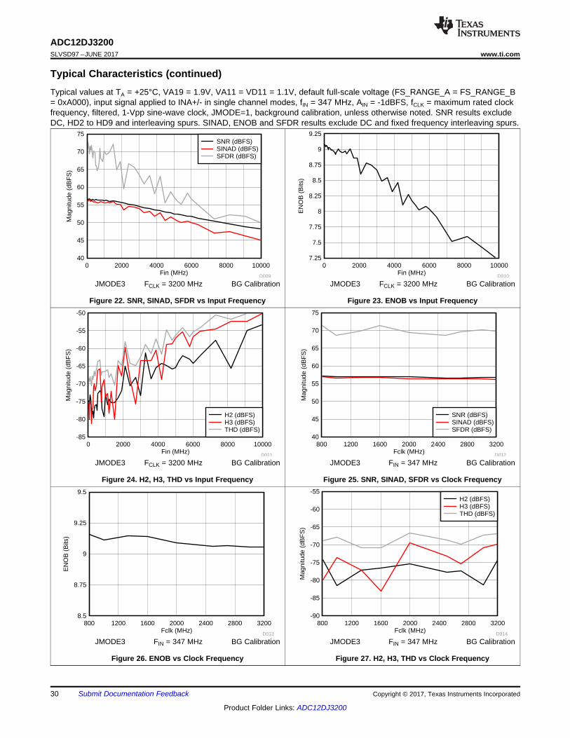
Fclk (MHz)
EN
OB
(B
its)
800 1200 1600 2000 2400 2800 32008.5
8.75
9
9.25
9.5
D013Fclk (MHz)
Mag
nitu
de (
dBF
S)
800 1200 1600 2000 2400 2800 3200-90
-85
-80
-75
-70
-65
-60
-55
D014
H2 (dBFS)H3 (dBFS)THD (dBFS)
Fin (MHz)
Mag
nitu
de (
dBF
S)
0 2000 4000 6000 8000 10000-85
-80
-75
-70
-65
-60
-55
-50
D011
H2 (dBFS)H3 (dBFS)THD (dBFS)
Fclk (MHz)
Mag
nitu
de (
dBF
S)
800 1200 1600 2000 2400 2800 320040
45
50
55
60
65
70
75
D012
SNR (dBFS)SINAD (dBFS)SFDR (dBFS)
Fin (MHz)
Mag
nitu
de (
dBF
S)
0 2000 4000 6000 8000 1000040
45
50
55
60
65
70
75
D009
SNR (dBFS)SINAD (dBFS)SFDR (dBFS)
Fin (MHz)
EN
OB
(B
its)
0 2000 4000 6000 8000 100007.25
7.5
7.75
8
8.25
8.5
8.75
9
9.25
D010
30
ADC12DJ3200SLVSD97 –JUNE 2017 www.ti.com
Product Folder Links: ADC12DJ3200
Submit Documentation Feedback Copyright © 2017, Texas Instruments Incorporated
Typical Characteristics (continued)Typical values at TA = +25°C, VA19 = 1.9V, VA11 = VD11 = 1.1V, default full-scale voltage (FS_RANGE_A = FS_RANGE_B= 0xA000), input signal applied to INA+/- in single channel modes, fIN = 347 MHz, AIN = -1dBFS, fCLK = maximum rated clockfrequency, filtered, 1-Vpp sine-wave clock, JMODE=1, background calibration, unless otherwise noted. SNR results excludeDC, HD2 to HD9 and interleaving spurs. SINAD, ENOB and SFDR results exclude DC and fixed frequency interleaving spurs.
JMODE3 FCLK = 3200 MHz BG Calibration
Figure 22. SNR, SINAD, SFDR vs Input Frequency
JMODE3 FCLK = 3200 MHz BG Calibration
Figure 23. ENOB vs Input Frequency
JMODE3 FCLK = 3200 MHz BG Calibration
Figure 24. H2, H3, THD vs Input Frequency
JMODE3 FIN = 347 MHz BG Calibration
Figure 25. SNR, SINAD, SFDR vs Clock Frequency
JMODE3 FIN = 347 MHz BG Calibration
Figure 26. ENOB vs Clock Frequency
JMODE3 FIN = 347 MHz BG Calibration
Figure 27. H2, H3, THD vs Clock Frequency
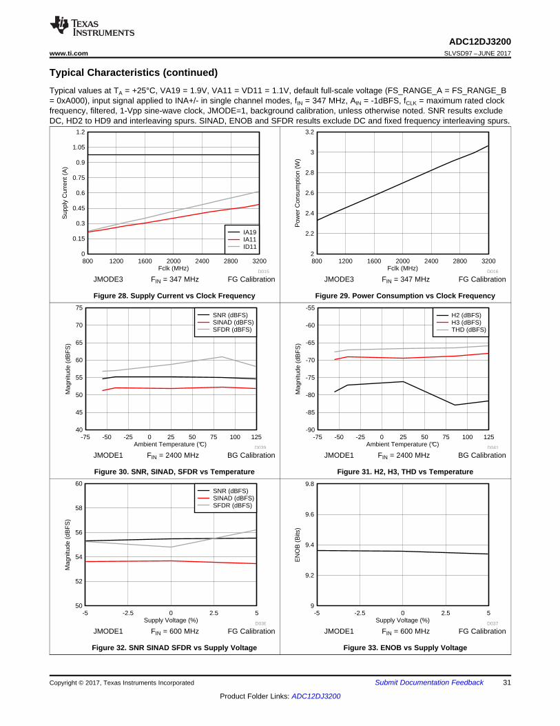
Supply Voltage (%)
Mag
nitu
de (
dBF
S)
-5 -2.5 0 2.5 550
52
54
56
58
60
D036
SNR (dBFS)SINAD (dBFS)SFDR (dBFS)
Supply Voltage (%)
EN
OB
(B
its)
-5 -2.5 0 2.5 59
9.2
9.4
9.6
9.8
D037
Ambient Temperature (°C)
Mag
nitu
de (
dBF
S)
-75 -50 -25 0 25 50 75 100 12540
45
50
55
60
65
70
75
D039
SNR (dBFS)SINAD (dBFS)SFDR (dBFS)
Ambient Temperature (°C)
Mag
nitu
de (
dBF
S)
-75 -50 -25 0 25 50 75 100 125-90
-85
-80
-75
-70
-65
-60
-55
D041
H2 (dBFS)H3 (dBFS)THD (dBFS)
Fclk (MHz)
Sup
ply
Cur
rent
(A
)
800 1200 1600 2000 2400 2800 32000
0.15
0.3
0.45
0.6
0.75
0.9
1.05
1.2
D015
IA19IA11ID11
Fclk (MHz)
Pow
er C
onsu
mpt
ion
(W)
800 1200 1600 2000 2400 2800 32002
2.2
2.4
2.6
2.8
3
3.2
D016
31
ADC12DJ3200www.ti.com SLVSD97 –JUNE 2017
Product Folder Links: ADC12DJ3200
Submit Documentation FeedbackCopyright © 2017, Texas Instruments Incorporated
Typical Characteristics (continued)Typical values at TA = +25°C, VA19 = 1.9V, VA11 = VD11 = 1.1V, default full-scale voltage (FS_RANGE_A = FS_RANGE_B= 0xA000), input signal applied to INA+/- in single channel modes, fIN = 347 MHz, AIN = -1dBFS, fCLK = maximum rated clockfrequency, filtered, 1-Vpp sine-wave clock, JMODE=1, background calibration, unless otherwise noted. SNR results excludeDC, HD2 to HD9 and interleaving spurs. SINAD, ENOB and SFDR results exclude DC and fixed frequency interleaving spurs.
JMODE3 FIN = 347 MHz FG Calibration
Figure 28. Supply Current vs Clock Frequency
JMODE3 FIN = 347 MHz FG Calibration
Figure 29. Power Consumption vs Clock Frequency
JMODE1 FIN = 2400 MHz BG Calibration
Figure 30. SNR, SINAD, SFDR vs Temperature
JMODE1 FIN = 2400 MHz BG Calibration
Figure 31. H2, H3, THD vs Temperature
JMODE1 FIN = 600 MHz FG Calibration
Figure 32. SNR SINAD SFDR vs Supply Voltage
JMODE1 FIN = 600 MHz FG Calibration
Figure 33. ENOB vs Supply Voltage
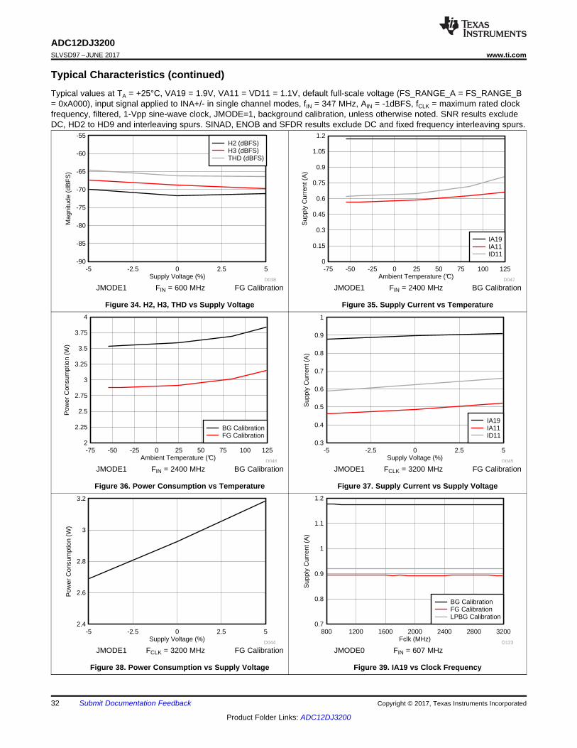
Supply Voltage (%)
Pow
er C
onsu
mpt
ion
(W)
-5 -2.5 0 2.5 52.4
2.6
2.8
3
3.2
D044Fclk (MHz)
Sup
ply
Cur
rent
(A
)
800 1200 1600 2000 2400 2800 32000.7
0.8
0.9
1
1.1
1.2
D123
BG CalibrationFG CalibrationLPBG Calibration
Ambient Temperature (°C)
Pow
er C
onsu
mpt
ion
(W)
-75 -50 -25 0 25 50 75 100 1252
2.25
2.5
2.75
3
3.25
3.5
3.75
4
D046
BG CalibrationFG Calibration
Supply Voltage (%)
Sup
ply
Cur
rent
(A
)
-5 -2.5 0 2.5 50.3
0.4
0.5
0.6
0.7
0.8
0.9
1
D045
IA19IA11ID11
Supply Voltage (%)
Mag
nitu
de (
dBF
S)
-5 -2.5 0 2.5 5-90
-85
-80
-75
-70
-65
-60
-55
D038
H2 (dBFS)H3 (dBFS)THD (dBFS)
Ambient Temperature (°C)
Sup
ply
Cur
rent
(A
)
-75 -50 -25 0 25 50 75 100 1250
0.15
0.3
0.45
0.6
0.75
0.9
1.05
1.2
D047
IA19IA11ID11
32
ADC12DJ3200SLVSD97 –JUNE 2017 www.ti.com
Product Folder Links: ADC12DJ3200
Submit Documentation Feedback Copyright © 2017, Texas Instruments Incorporated
Typical Characteristics (continued)Typical values at TA = +25°C, VA19 = 1.9V, VA11 = VD11 = 1.1V, default full-scale voltage (FS_RANGE_A = FS_RANGE_B= 0xA000), input signal applied to INA+/- in single channel modes, fIN = 347 MHz, AIN = -1dBFS, fCLK = maximum rated clockfrequency, filtered, 1-Vpp sine-wave clock, JMODE=1, background calibration, unless otherwise noted. SNR results excludeDC, HD2 to HD9 and interleaving spurs. SINAD, ENOB and SFDR results exclude DC and fixed frequency interleaving spurs.
JMODE1 FIN = 600 MHz FG Calibration
Figure 34. H2, H3, THD vs Supply Voltage
JMODE1 FIN = 2400 MHz BG Calibration
Figure 35. Supply Current vs Temperature
JMODE1 FIN = 2400 MHz BG Calibration
Figure 36. Power Consumption vs Temperature
JMODE1 FCLK = 3200 MHz FG Calibration
Figure 37. Supply Current vs Supply Voltage
JMODE1 FCLK = 3200 MHz FG Calibration
Figure 38. Power Consumption vs Supply Voltage
JMODE0 FIN = 607 MHz
Figure 39. IA19 vs Clock Frequency

Decimation Factor
EN
OB
(B
its)
1 2 3 4 5 6 7 8 9 10 11 12 13 14 15 168.5
9
9.5
10
10.5
D133
FIN = 2400 MHzFIN = 600 MHz
JMODE
Sup
ply
Cur
rent
(A
)
0 2 4 6 8 10 12 14 16 180
0.25
0.5
0.75
1
1.25
1.5
D034
IA11ID11IA19
Fclk (MHz)
Pow
er C
onsu
mpt
ion
(W)
800 1200 1600 2000 2400 2800 32002
2.5
3
3.5
4
D118
BG CalibrationFG CalibrationLPBG Calibration
Decimation Factor
Mag
nitu
de (
dBF
S)
1 2 3 4 5 6 7 8 9 10 11 12 13 14 15 1645
50
55
60
65
70
75
80
85
D035
SNR (dBFS)SINAD (dBFS)SFDR (dBFS)
Fclk (MHz)
Sup
ply
Cur
rent
(A
)
800 1200 1600 2000 2400 2800 32000
0.2
0.4
0.6
0.8
D124
BG CalibrationFG CalibrationLPBG Calibration
Fclk (MHz)
Sup
ply
Cur
rent
(A
)
800 1200 1600 2000 2400 2800 32000
0.2
0.4
0.6
0.8
D117
BG CalibrationFG CalibrationLPBG Calibration
33
ADC12DJ3200www.ti.com SLVSD97 –JUNE 2017
Product Folder Links: ADC12DJ3200
Submit Documentation FeedbackCopyright © 2017, Texas Instruments Incorporated
Typical Characteristics (continued)Typical values at TA = +25°C, VA19 = 1.9V, VA11 = VD11 = 1.1V, default full-scale voltage (FS_RANGE_A = FS_RANGE_B= 0xA000), input signal applied to INA+/- in single channel modes, fIN = 347 MHz, AIN = -1dBFS, fCLK = maximum rated clockfrequency, filtered, 1-Vpp sine-wave clock, JMODE=1, background calibration, unless otherwise noted. SNR results excludeDC, HD2 to HD9 and interleaving spurs. SINAD, ENOB and SFDR results exclude DC and fixed frequency interleaving spurs.
JMODE0 FIN = 607 MHz
Figure 40. IA11 vs Clock Frequency
JMODE0 FIN = 607 MHz
Figure 41. ID11 vs Clock Frequency
JMODE0 FIN = 607 MHz
Figure 42. Power Consumption vs Clock Frequency
FCLK = 3200 MHz FIN = 2400 MHz FG Calibration
Figure 43. SNR, SINAD, SFDR vs DECIMATION FACTOR
FCLK = 3200 MHz FG Calibration
Figure 44. ENOB vs DECIMATION FACTOR
FIN = 2400 MHz FCLK = 3200 MHz FG Calibration
Figure 45. Supply Current vs JMODE
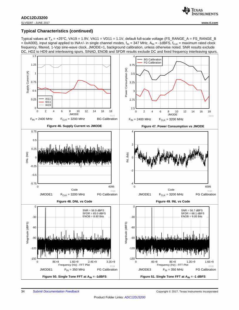
Frequency (Hz) - FFT Plot
Mag
nitu
de (
dBF
S)
0 8E+8 1.6E+9 2.4E+9 3.2E+9-150
-120
-90
-60
-30
0SNR = 56.9 dBFSSFDR = 65.0 dBFSENOB = 8.80 Bits
D134Frequency (Hz) - FFT Plot
Mag
nitu
de (
dBF
S)
0 4E+8 8E+8 1.2E+9 1.6E+9-150
-120
-90
-60
-30
0SNR = 56.7 dBFSSFDR = 68.1 dBFSENOB = 9.05 Bits
D139
Code
DN
L (ls
b)
0 4095-0.75
-0.5
-0.25
0
0.25
0.5
0.75
D048Code
INL
(lsb)
0 4095-4
-2
0
2
4
D049
JMODE
Pow
er C
onsu
mpt
ion
(W)
0 2 4 6 8 10 12 14 16 182.5
2.75
3
3.25
3.5
3.75
4
D033
BG CalibrationFG Calibration
JMODE
Sup
ply
Cur
rent
(A
)
0 2 4 6 8 10 12 14 16 180
0.25
0.5
0.75
1
1.25
1.5
D122
IA11ID11IA19
34
ADC12DJ3200SLVSD97 –JUNE 2017 www.ti.com
Product Folder Links: ADC12DJ3200
Submit Documentation Feedback Copyright © 2017, Texas Instruments Incorporated
Typical Characteristics (continued)Typical values at TA = +25°C, VA19 = 1.9V, VA11 = VD11 = 1.1V, default full-scale voltage (FS_RANGE_A = FS_RANGE_B= 0xA000), input signal applied to INA+/- in single channel modes, fIN = 347 MHz, AIN = -1dBFS, fCLK = maximum rated clockfrequency, filtered, 1-Vpp sine-wave clock, JMODE=1, background calibration, unless otherwise noted. SNR results excludeDC, HD2 to HD9 and interleaving spurs. SINAD, ENOB and SFDR results exclude DC and fixed frequency interleaving spurs.
FIN = 2400 MHz FCLK = 3200 MHz BG Calibration
Figure 46. Supply Current vs JMODE
FIN = 2400 MHz FCLK = 3200 MHz
Figure 47. Power Consumption vs JMODE
JMODE1 FCLK = 3200 MHz FG Calibration
Figure 48. DNL vs Code
JMODE1 FCLK = 3200 MHz FG Calibration
Figure 49. INL vs Code
JMODE1 FIN = 350 MHz FG Calibration
Figure 50. Single Tone FFT at AIN = -1dBFS
JMODE3 FIN = 350 MHz FG Calibration
Figure 51. Single Tone FFT at AIN = -1 dBFS

Frequency (Hz) - FFT Plot
Mag
nitu
de (
dBF
S)
0 4E+8 8E+8 1.2E+9 1.6E+9-150
-120
-90
-60
-30
0SNR = 50.4 dBFSSFDR = 52.3 dBFSENOB = 7.68 Bits
D145Frequency (Hz) - FFT Plot
Mag
nitu
de (
dBF
S)
0 8E+8 1.6E+9 2.4E+9 3.2E+9-150
-120
-90
-60
-30
0SNR = 51.0 dBFSSFDR = 54.9 dBFSENOB = 7.77 Bits
D144
Frequency (Hz) - FFT Plot
Mag
nitu
de (
dBF
S)
0 8E+8 1.6E+9 2.4E+9 3.2E+9-150
-120
-90
-60
-30
0SNR = 53.5 dBFSSFDR = 53.5 dBFSENOB = 7.89 Bits
D136Frequency (Hz) - FFT Plot
Mag
nitu
de (
dBF
S)
0 4E+8 8E+8 1.2E+9 1.6E+9-150
-120
-90
-60
-30
0SNR = 52.8 dBFSSFDR = 54.3 dBFSENOB = 7.93 Bits
D141
Frequency (Hz) - FFT Plot
Mag
nitu
de (
dBF
S)
0 8E+8 1.6E+9 2.4E+9 3.2E+9-150
-120
-90
-60
-30
0SNR = 55.5 dBFSSFDR = 56.0 dBFSENOB = 8.55 Bits
D135Frequency (Hz) - FFT Plot
Mag
nitu
de (
dBF
S)
0 4E+8 8E+8 1.2E+9 1.6E+9-150
-120
-90
-60
-30
0SNR = 55.0 dBFSSFDR = 59.1 dBFSENOB = 8.57 Bits
D140
35
ADC12DJ3200www.ti.com SLVSD97 –JUNE 2017
Product Folder Links: ADC12DJ3200
Submit Documentation FeedbackCopyright © 2017, Texas Instruments Incorporated
Typical Characteristics (continued)Typical values at TA = +25°C, VA19 = 1.9V, VA11 = VD11 = 1.1V, default full-scale voltage (FS_RANGE_A = FS_RANGE_B= 0xA000), input signal applied to INA+/- in single channel modes, fIN = 347 MHz, AIN = -1dBFS, fCLK = maximum rated clockfrequency, filtered, 1-Vpp sine-wave clock, JMODE=1, background calibration, unless otherwise noted. SNR results excludeDC, HD2 to HD9 and interleaving spurs. SINAD, ENOB and SFDR results exclude DC and fixed frequency interleaving spurs.
JMODE1 FIN = 2700 MHz FG Calibration
Figure 52. Single Tone FFT at AIN = -1 dBFS
JMODE3 FIN = 2700 MHz FG Calibration
Figure 53. Single Tone FFT at AIN = -1 dBFS
JMODE1 FIN = 5000 MHz FG Calibration
Figure 54. Single Tone FFT at AIN = -1 dBFS
JMODE3 FIN = 5000 MHz FG Calibration
Figure 55. Single Tone FFT at AIN = -1 dBFS
JMODE1 FIN = 8200 MHz FG Calibration
Figure 56. Single Tone FFT at AIN = -1 dBFS
JMODE3 FIN = 8200 MHz FG Calibration
Figure 57. Single Tone FFT at AIN = -1 dBFS

Sample Number
Sam
ple
Val
ue
0 5000 10000 15000 20000 25000 30000 350000
500
1000
1500
2000
2500
3000
3500
4000
Zoomed Area in Following Plot
D125Sample Number
Sam
ple
Val
ue
14400 14800 15200 15600 16000 16400150015501600165017001750180018501900195020002050210021502200
D126
Frequency (Hz) - FFT Plot
Mag
nitu
de (
dBF
S)
0 8E+8 1.6E+9 2.4E+9 3.2E+9-150
-120
-90
-60
-30
0SNR = 57.3 dBFSSFDR = 67.6 dBFSENOB = 8.71 Bits
D137Frequency (Hz) - FFT Plot
Mag
nitu
de (
dBF
S)
0 4E+8 8E+8 1.2E+9 1.6E+9-150
-120
-90
-60
-30
0SNR = 57.1 dBFSSFDR = 73.9 dBFSENOB = 9.13 Bits
D142
36
ADC12DJ3200SLVSD97 –JUNE 2017 www.ti.com
Product Folder Links: ADC12DJ3200
Submit Documentation Feedback Copyright © 2017, Texas Instruments Incorporated
Typical Characteristics (continued)Typical values at TA = +25°C, VA19 = 1.9V, VA11 = VD11 = 1.1V, default full-scale voltage (FS_RANGE_A = FS_RANGE_B= 0xA000), input signal applied to INA+/- in single channel modes, fIN = 347 MHz, AIN = -1dBFS, fCLK = maximum rated clockfrequency, filtered, 1-Vpp sine-wave clock, JMODE=1, background calibration, unless otherwise noted. SNR results excludeDC, HD2 to HD9 and interleaving spurs. SINAD, ENOB and SFDR results exclude DC and fixed frequency interleaving spurs.
JMODE1 FIN = 8200 MHz FG Calibration
Figure 58. Single Tone FFT at AIN = -16 dBFS
JMODE3 FIN = 8200 MHz FG Calibration
Figure 59. Single Tone FFT at AIN = -16 dBFS
JMODE2 FCLK = 3200 MHz FIN = 3199.9 MHz
Figure 60. Background Calibration Core Transition - ACSignal
JMODE2 FCLK = 3200 MHz FIN = 3199.9 MHz
Figure 61. Background Calibration Core Transition - ACSignal Zoomed

Sample Number
Sam
ple
Val
ue
1500 1650 1800 1950 2100 2250 2400 25500
50
100
150
200
250
300
350
400
450
500
D128
-0.35V Differential
Sample Number
Sam
ple
Val
ue
0 1000 2000 3000 4000 5000 6000 7000 80000
250500750
1000125015001750200022502500275030003250350037504000
D127
+0.35V Differential-0.35V Differential0V Differential
37
ADC12DJ3200www.ti.com SLVSD97 –JUNE 2017
Product Folder Links: ADC12DJ3200
Submit Documentation FeedbackCopyright © 2017, Texas Instruments Incorporated
Typical Characteristics (continued)Typical values at TA = +25°C, VA19 = 1.9V, VA11 = VD11 = 1.1V, default full-scale voltage (FS_RANGE_A = FS_RANGE_B= 0xA000), input signal applied to INA+/- in single channel modes, fIN = 347 MHz, AIN = -1dBFS, fCLK = maximum rated clockfrequency, filtered, 1-Vpp sine-wave clock, JMODE=1, background calibration, unless otherwise noted. SNR results excludeDC, HD2 to HD9 and interleaving spurs. SINAD, ENOB and SFDR results exclude DC and fixed frequency interleaving spurs.
JMODE0 FCLK = 3200 MHz DC Input
Figure 62. Background Calibration Core Transition - DCSignal
JMODE0 FCLK = 3200 MHz DC Input
Figure 63. Background Calibration Core Transition - DCSignal Zoomed

38
ADC12DJ3200SLVSD97 –JUNE 2017 www.ti.com
Product Folder Links: ADC12DJ3200
Submit Documentation Feedback Copyright © 2017, Texas Instruments Incorporated
7 Detailed Description
7.1 OverviewADC12DJ3200 is an RF-sampling giga-sample ADC that can directly sample input frequencies from DC to above10 GHz. In dual channel mode, ADC12DJ3200 can sample up to 3200-MSPS and in single channel mode up to6400-MSPS. Programmable tradeoffs in channel count (dual channel mode) and Nyquist bandwidth (singlechannel mode) allow development of flexible hardware that meets the needs of both high channel count or wideinstantaneous signal bandwidth applications. Full power input bandwidth (-3 dB) of 8.0 GHz, with usablefrequencies exceeding the -3 dB point in both dual and single channel modes, allows direct RF sampling of L-band, S-band, C-band and X-band for frequency agile systems.
Time interleaving is achieved internally through 4 active cores. In dual channel mode, two cores are interleavedper channel to increase the sample rate to 2x the core sample rate. In single channel mode, all 4 cores are timeinterleaved to increase the sample rate to 4x the core sample rate. Either input can be used in single channelmode, however performance has been optimized for INA+/–. The user provides a clock at 2x the ADC coresample rate and the generation of the clocks for the interleaved cores is done internally for both single channelmode and dual channel mode. ADC12DJ3200 also provides foreground and background calibration options tomatch the gain and offset between cores to minimize spurious artifacts due to the interleaving.
ADC12DJ3200 uses a high speed JESD204B output interface with up to 16 serialized lanes and subclass-1compliance for deterministic latency and multi-device synchronization. The serial output lanes support up to 12.8Gbps and can be configured to trade-off bit rate and number of lanes. Innovative synchronization features,including noiseless aperture delay (TAD) adjustment and SYSREF windowing, simplify system design for phasedarray radar and MIMO communications. Optional digital down converters (DDCs) in dual channel mode allow forreduction in interface rate (real and complex decimation modes) and digital mixing of the signal (complexdecimation modes only).
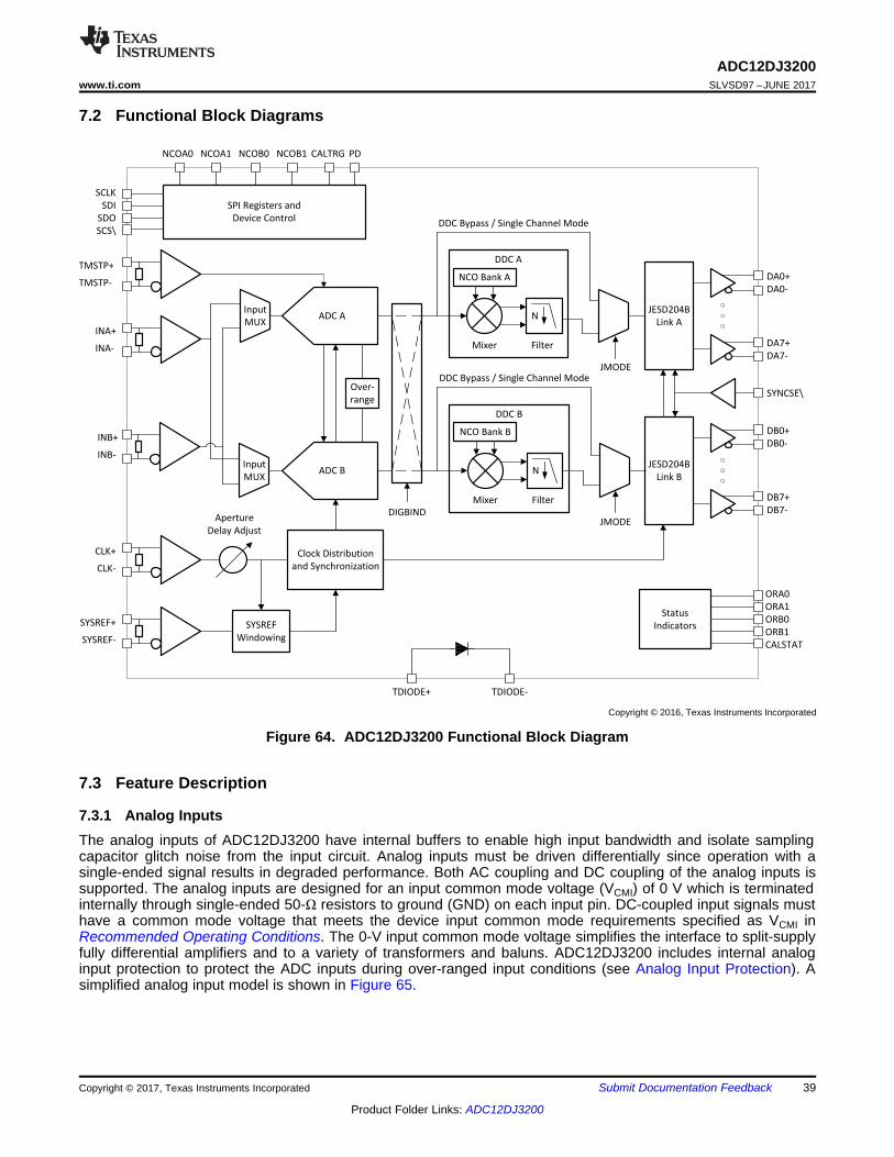
DDC Bypass / Single Channel Mode
SCLK
SDI
SDO
SCS\
NCOA0 NCOA1 NCOB0 NCOB1
ADC AJESD204B
Link A
JESD204B
Link B
Aperture
Delay Adjust
Clock Distribution
and Synchronization
CLK+
CLK-
SYSREF+
SYSREF-
SYNCSE\Over-
range
DA0+
DA0-
DA7+
DA7-
DB0+
DB0-
DB7+
DB7-
Status
Indicators
ORA0
ORA1
ORB0
ORB1
CALSTAT
ADC B
TDIODE+ TDIODE-
CALTRG PD
SPI Registers and
Device Control
INA+
INA-
INB+
INB-
TMSTP+
TMSTP-
Input
MUX
Input
MUX
DDC A
Mixer Filter
N
NCO Bank A
DDC Bypass / Single Channel Mode
DDC B
Mixer Filter
N
NCO Bank B
JMODE
JMODE
SYSREF
Windowing
DIGBIND
Copyright © 2016, Texas Instruments Incorporated
39
ADC12DJ3200www.ti.com SLVSD97 –JUNE 2017
Product Folder Links: ADC12DJ3200
Submit Documentation FeedbackCopyright © 2017, Texas Instruments Incorporated
7.2 Functional Block Diagrams
Figure 64. ADC12DJ3200 Functional Block Diagram
7.3 Feature Description
7.3.1 Analog InputsThe analog inputs of ADC12DJ3200 have internal buffers to enable high input bandwidth and isolate samplingcapacitor glitch noise from the input circuit. Analog inputs must be driven differentially since operation with asingle-ended signal results in degraded performance. Both AC coupling and DC coupling of the analog inputs issupported. The analog inputs are designed for an input common mode voltage (VCMI) of 0 V which is terminatedinternally through single-ended 50-Ω resistors to ground (GND) on each input pin. DC-coupled input signals musthave a common mode voltage that meets the device input common mode requirements specified as VCMI inRecommended Operating Conditions. The 0-V input common mode voltage simplifies the interface to split-supplyfully differential amplifiers and to a variety of transformers and baluns. ADC12DJ3200 includes internal analoginput protection to protect the ADC inputs during over-ranged input conditions (see Analog Input Protection). Asimplified analog input model is shown in Figure 65.

ADC
50
50
INA/B+
INA/B-
AGND
Analog input
protection
diodes
Input buffer
Copyright © 2016, Texas Instruments Incorporated
40
ADC12DJ3200SLVSD97 –JUNE 2017 www.ti.com
Product Folder Links: ADC12DJ3200
Submit Documentation Feedback Copyright © 2017, Texas Instruments Incorporated
Feature Description (continued)
Figure 65. ADC12DJ3200 Analog Input Internal Termination and Protection
There is minimal degradation in analog input bandwidth when using single channel mode versus dual channelmode. In single channel mode it is strongly recommended that INA+/– be used as the input to the ADC sinceADC performance has been optimized for INA+/–. However, either analog input (INA+ and INA– or INB+ andINB–) can be used. The use of INB+/– will result in degraded performance unless custom trim routines are usedto optimize performance for INB+/– for each device. The desired input can be chosen using SINGLE_INPUT inInput Mux Control Register (address = 0x060) [reset = 0x01].
NOTEIn single channel mode it is strongly recommended that INA+/– be used as the input to theADC for optimized performance.
7.3.1.1 Analog Input ProtectionThe analog inputs are protected against over-drive conditions by internal clamping diodes that are capable ofsourcing or sinking input currents during over-range conditions, see voltage and current limits in AbsoluteMaximum Ratings. The over-range protection is also defined for a peak RF input power in Absolute MaximumRatings, which is frequency independent. Operation above the maximum conditions listed in RecommendedOperating Conditions will result in an increase in failure-in-time (FIT) rate, so the system should correct the over-drive condition as quickly as possible. The analog input protection diodes are shown in Figure 65.
7.3.1.2 Full-Scale Voltage (VFS) AdjustmentInput full-scale voltage (VFS) adjustment is available, in fine increments, for each analog input through theFS_RANGE_A (INA Full Scale Range Adjust Register (address = 0x030-0x031) [reset = 0xA000]) register settingand FS_RANGE_B (INB Full Scale Range Adjust Register (address = 0x032-0x033) [reset = 0xA000]) registersetting for INA+/– and INB+/–, respectively. The available adjustment range is specified in ElectricalCharacteristics - DC Specifications. Larger full-scale voltages improve SNR and noise floor (in dBFS/Hz)performance, but may degrade harmonic distortion. The full-scale voltage adjustment is useful for matching thefull-scale range of multiple ADCs when developing a multi-converter system or for external interleaving ofmultiple ADC12DJ3200 to achieve higher sampling rates.
7.3.1.3 Analog Input Offset AdjustThe input offset voltage for each input can be adjusted through the OADJ_x_INy registers (registers 0x08A and0x095), where x represents the ADC core (A, B, or C) and y represents the analog input (INA+/– or INB+/–). Theadjustment range is approximately 28 mV to –28 mV differential. See Calibration Modes and Trimming for moreinformation.

FSNIN VCode
V2
41
ADC12DJ3200www.ti.com SLVSD97 –JUNE 2017
Product Folder Links: ADC12DJ3200
Submit Documentation FeedbackCopyright © 2017, Texas Instruments Incorporated
Feature Description (continued)7.3.2 ADC CoreADC12DJ3200 consists of a total of six ADC cores. The cores are interleaved for higher sampling rates andswapped on-the-fly for calibration as required by the operating mode. This section highlights the theory and keyfeatures of the ADC cores.
7.3.2.1 ADC Theory of OperationThe differential voltages at the analog inputs are captured by the rising edge of CLK+/– in dual channel mode orby the rising and falling edges of CLK+/– in single channel mode. After capturing the input signal, the ADCconverts the analog voltage to a digital value by comparing the voltage to the internal reference voltage. If thevoltage on INA– or INB– is higher than the voltage on INA+ or INB+, respectively, then the digital output will be anegative 2's complement value. If the voltage on INA+ or INB+ is higher than the voltage on INA– or INB–,respectively, then the digital output will be a positive 2's complement value. The differential voltage at the inputpins can be calculated from the digital output by Equation 1 where Code is the signed decimation output code(e.g. –2048 to +2047), N is the ADC resolution and VFS is the full-scale input voltage of the ADC as specified inRecommended Operating Conditions, including any adjustment performed by programming FS_RANGE_A orFS_RANGE_B.
(1)
7.3.2.2 ADC Core CalibrationADC core calibration is required to optimize analog performance of the ADC cores. Calibration must be repeatedas operating conditions change significantly, namely temperature, in order to maintain optimal performance. TheADC12DJ3200 family has a built in calibration routine that can be run as a foreground operation or a backgroundoperation. Foreground operation requires ADC downtime, where the ADC is no longer sampling the input signal,to complete the process. Background calibration can be used to overcome this limitation and allow constantoperation of the ADC. See Calibration Modes and Trimming for detailed information on each mode.
7.3.2.3 ADC Over-Range DetectionTo ensure that system gain management has the quickest-possible response time, a low-latency configurableover-range function is included. The over-range function works by monitoring the converted 12-bit samples at theADC to quickly detect if the ADC is near saturation or already in an over-range condition. The absolute value ofthe upper 8 bits of the ADC data are checked against two programmable thresholds, OVR_T0 and OVR_T1.These thresholds apply to both channel A and channel B in dual channel mode. The following table lists how anADC sample is converted to an absolute value for a comparison of the thresholds.
Table 1. Conversion of ADC Sample for Over-Range ComparisonADC SAMPLE(OFFSET BINARY)
ADC SAMPLE(2's COMPLEMENT) ABSOLUTE VALUE UPPER 8 BITS USED FOR
COMPARISON1111 1111 1111 (4095) 0111 1111 1111 (+2047) 111 1111 1111 (2047) 1111 1111 (255)1111 1111 0000 (4080) 0111 1111 0000 (+2032) 111 1111 0000 (2032) 1111 1110 (254)1000 0000 0000 (2048) 0000 0000 0000 (0) 000 0000 0000 (0) 0000 0000 (0)0000 0001 0000 (16) 1000 0001 0000 (–2032) 111 1111 0000 (2032) 1111 1110 (254)0000 0000 0000 (0) 1000 0000 0000 (–2048) 111 1111 1111 (2047) 1111 1111 (255)
If the upper 8 bits of the absolute value equal or exceed the OVR_T0 or OVR_T1 thresholds during themonitoring period, then the over-range bit associated with the threshold is set to 1, otherwise the over-range bitis 0. In dual channel mode the over-range status can be monitored on the ORA0 and ORA1 pins for channel Aand ORB0 and ORB1 pins for channel B, where ORx0 corresponds to the OVR_T0 threshold and ORx1corresponds to the OVR_T1 threshold. In single channel mode the over-range status for threshold OVR_T0 isdetermined by monitoring both ORA0 and ORB0 outputs while the OVR_T1 threshold is determined bymonitoring both ORA1 and ORB1 outputs. In single channel mode the two outputs for each threshold should beOR'd together to determine whether an over-range condition occurred. OVR_N can be used to set the outputpulse duration from the last over-range event. Table 2 lists the over-range pulse lengths for the various OVR_Nsettings (Over-range Configuration Register (address = 0x213) [reset = 0x07]). In decimation modes (only in the

42
ADC12DJ3200SLVSD97 –JUNE 2017 www.ti.com
Product Folder Links: ADC12DJ3200
Submit Documentation Feedback Copyright © 2017, Texas Instruments Incorporated
JMODEs where CS = 1 in Table 18), the over-range status is also embedded into the output data samples. Forcomplex decimation modes the OVR_T0 threshold status is embedded as the LSB along with the upper 15 bitsof every complex I sample and OVR_T1 threshold status is embedded as the LSB along with the upper 15 bits ofevery complex Q sample. For real decimation modes the OVR_T0 threshold status is embedded as the LSB ofevery even numbered sample and OVR_T1 threshold status is embedded as the LSB of every odd numberedsample. Table 3 lists the outputs, related data samples, threshold settings and the monitoring period equation.The embedded over-range bit will go high if the associated channel has exceeded the associated over-rangethreshold within the monitoring period set by OVR_N. The monitoring period can be calculated as shown inTable 3..
Table 2. Over-Range Monitoring Period for ORA0, ORA1, ORB0 and ORB1Outputs
OVR_N OVER-RANGE PULSE LENGTH SINCE LASTOVER-RANGE EVENT (DEVCLK CYCLES)
0 81 162 323 644 1285 2566 5127 1024
(1) OVR_N is the monitoring period register setting.
Table 3. Threshold and Monitoring Period for Embedded Over-Range Indicators in Dual ChannelDecimation Modes
OVER-RANGEINDICATOR
ASSOCIATEDTHRESHOLD DECIMATION TYPE OVER-RANGE STATUS
EMBEDDED INMONITORING PERIOD
(ADC SAMPLES)
ORA0 OVR_T0Real Decimation (JMODE 9) Channel A even
numbered samples 2OVR_N+1(1)
Complex Down-Conversion (JMODE10-16, except JMODE 12)
Channel A In-Phase (I)samples 2OVR_N(1)
ORA1 OVR_T1Real Decimation (JMODE 9) Channel A odd
numbered samples 2OVR_N+1(1)
Complex Down-Conversion (JMODE10-16, except JMODE 12)
Channel A Quadrature(Q) samples 2OVR_N(1)
ORB0 OVR_T0Real Decimation (JMODE 9) Channel B even
numbered samples 2OVR_N+1(1)
Complex Down-Conversion (JMODE10-16, except JMODE 12)
Channel B In-Phase (I)samples 2OVR_N(1)
ORB1 OVR_T1Real Decimation (JMODE 9) Channel B odd
numbered samples 2OVR_N+1(1)
Complex Down-Conversion (JMODE10-16, except JMODE 12)
Channel B Quadrature(Q) samples 2OVR_N(1)
Typically, the OVR_T0 threshold can be set near the full-scale value (228 for example). When the threshold istriggered, a typical system can turn down the system gain to avoid clipping. The OVR_T1 threshold can be setmuch lower. For example, the OVR_T1 threshold can be set to 64 (peak input voltage of −12 dBFS). If the inputsignal is strong, the OVR_T1 threshold is tripped occasionally. If the input is quite weak, the threshold is nevertripped. The downstream logic device monitors the OVR_T1 bit. If OVR_T1 stays low for an extended period oftime, then the system gain can be increased until the threshold is occasionally tripped (meaning the peak level ofthe signal is above −12 dBFS).

SYSREF Capture
tAD AdjustClock Distribution
and Synchronization
(ADC cores, digital,
JESD204B, etc.)
CLK+
CLK-
SYSREF+
SYSREF-SYSREF Windowing
Automatic
SYSREF
Calibration
SYSREF_POS SYSREF_SEL
TAD_INV
TAD_COARSE
TAD_FIN
E
SRC_EN
Duty Cycle
Correction
Copyright © 2016, Texas Instruments Incorporated
43
ADC12DJ3200www.ti.com SLVSD97 –JUNE 2017
Product Folder Links: ADC12DJ3200
Submit Documentation FeedbackCopyright © 2017, Texas Instruments Incorporated
7.3.2.4 Code Error Rate (CER)ADC cores can generate bit errors within a sample, often called code errors (CER) or referred to as sparklecodes, due to metastability caused by non-ideal comparator limitations. The ADC12DJ3200 uses a unique ADCarchitecture that inherently allows significant code error rate improvements from traditional pipelined flash orsuccessive approximation register (SAR) ADCs. The code error rate of the ADC12DJ3200 is multiple orders ofmagnitude better than what can be achieved in alternative architectures at equivalent sampling rates providingsignificant signal reliability improvements.
7.3.3 TimestampTMSTP+ and TMSTP– differential input can be used as a time-stamp input to mark a specific sample based onthe timing of an external trigger event relative to the sampled signal. TIMESTAMP_EN (LSB Control Bit OutputRegister (address = 0x160) [reset = 0x00]) must be set in order to use the timestamp feature and output thetimestamp data. When enabled, the LSB of the 12-bit ADC digital output reports the status of the TMSTP+/–input. In effect, the 12-bit output sample consists of the upper 11-bits of the 12-bit converter and the LSB of the12-bit output sample is the output of a parallel 1-bit converter (TMSTP+/–)with the same latency as the ADCcore. In the 8-bit operating modes, the LSB of the 8-bit output sample is used to output the timestamp status.The trigger must be applied to the differential TMSTP+ and TMSTP– inputs. The trigger can be asynchronous tothe ADC sampling clock and is sampled at approximately the same time as the analog input. Timestamp cannotbe used when a JMODE with decimation is selected and instead SYSREF should be used to achievesynchronization through JESD204B's subclass-1 method for achieving deterministic latency.
7.3.4 ClockingThe clocking subsystem of ADC12DJ3200 has two input signals, device clock (CLK+, CLK–) and SYSREF(SYSREF+, SYSREF–). Within the clocking subsystem there is a noiseless aperture delay adjustment (tADAdjust), a clock duty cycle corrector and a SYSREF capture block. The clocking subsystem is shown inFigure 66.
Figure 66. ADC12DJ3200 Clocking Subsystem
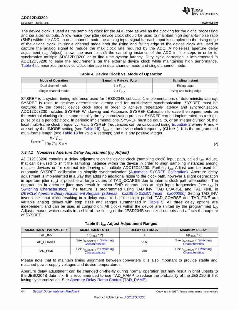
nKF
fRf CLK
SYSREFuuu
u
10
44
ADC12DJ3200SLVSD97 –JUNE 2017 www.ti.com
Product Folder Links: ADC12DJ3200
Submit Documentation Feedback Copyright © 2017, Texas Instruments Incorporated
The device clock is used as the sampling clock for the ADC core as well as the clocking for the digital processingand serializer outputs. A low noise (low jitter) device clock should be used to maintain high signal-to-noise ratio(SNR) within the ADC. In dual channel mode the analog input signal for each input is sampled on the rising edgeof the device clock. In single channel mode both the rising and falling edge of the device clock are used tocapture the analog signal to reduce the max clock rate required by the ADC. A noiseless aperture delayadjustment (tAD Adjust) allows the user to shift the sampling instance of the ADC in fine steps in order tosynchronize multiple ADC12DJ3200 or to fine tune system latency. Duty cycle correction is implemented inADC12DJ3200 to ease the requirements on the external device clock while maintaining high performance.Table 4 summarizes the device clock interface in dual channel mode and single channel mode.
Table 4. Device Clock vs. Mode of OperationMode of Operation Sampling Rate vs. FCLK Sampling InstantDual channel mode 1 x FCLK Rising edge
Single channel mode 2 x FCLK Rising and falling edge
SYSREF is a system timing reference used for JESD204B subclass-1 implementations of deterministic latency.SYSREF is used to achieve deterministic latency and for multi-device synchronization. SYSREF must becaptured by the correct device clock edge in order to achieve repeatable latency and synchronization.ADC12DJ3200 includes SYSREF Windowing and Automatic SYSREF Calibration to ease the requirements onthe external clocking circuits and simplify the synchronization process. SYSREF can be implemented as a singlepulse or as a periodic clock. In periodic implementations, SYSREF must be equal to, or an integer division of, thelocal multi-frame clock frequency. Valid SYSREF frequencies can be calculated using Equation 2 where R and Fare set by the JMODE setting (see Table 18), fCLK is the device clock frequency (CLK+/–), K is the programmedmulti-frame length (see Table 18 for valid K settings) and n is any positive integer.
(2)
7.3.4.1 Noiseless Aperture Delay Adjustment (tAD Adjust)ADC12DJ3200 contains a delay adjustment on the device clock (sampling clock) input path, called tAD Adjust,that can be used to shift the sampling instance within the device in order to align sampling instances amongmultiple devices or for external interleaving of multiple ADC12DJ3200. Further, tAD Adjust can be used forautomatic SYSREF calibration to simplify synchronization (Automatic SYSREF Calibration). Aperture delayadjustment is implemented in a way that adds no additional noise to the clock path, however a slight degradationin aperture jitter (tAJ) is possible at large values of TAD_COARSE due to internal clock path attenuation. Thedegradation in aperture jitter may result in minor SNR degradations at high input frequencies (see tAJ inSwitching Characteristics). The feature is programmed using TAD_INV, TAD_COARSE and TAD_FINE inDEVCLK Aperture Delay Adjustment Register (address = 0x2B5 to 0x2B7) [reset = 0x000000]. Setting TAD_INVinverts the input clock resulting in a delay equal to half the clock period. TAD_COARSE and TAD_FINE arevariable analog delays with step sizes and ranges summarized in Table 5. All three delay options areindependent and can be used in conjunction. All clocks within the device are shifted by the programmed tADAdjust amount, which results in a shift of the timing of the JESD204B serialized outputs and affects the captureof SYSREF.
Table 5. tAD Adjust Adjustment RangesADJUSTMENT PARAMETER ADJUSTMENT STEP DELAY SETTINGS MAXIMUM DELAY
TAD_INV 1/(FCLK * 2) 1 1/(FCLK * 2)
TAD_COARSE See tTAD(STEP) in SwitchingCharacteristics 256 See tTAD(MAX) in Switching
Characteristics
TAD_FINE See tTAD(STEP) in SwitchingCharacteristics 256 See tTAD(MAX) in Switching
Characteristics
Please note that to maintain timing alignment between converters it is also important to provide stable andmatched power supply voltages and device temperatures.
Aperture delay adjustment can be changed on-the-fly during normal operation but may result in brief upsets tothe JESD204B data link. It is recommended to use TAD_RAMP to reduce the probability of the JESD204B linklosing synchronization. See Aperture Delay Ramp Control (TAD_RAMP).
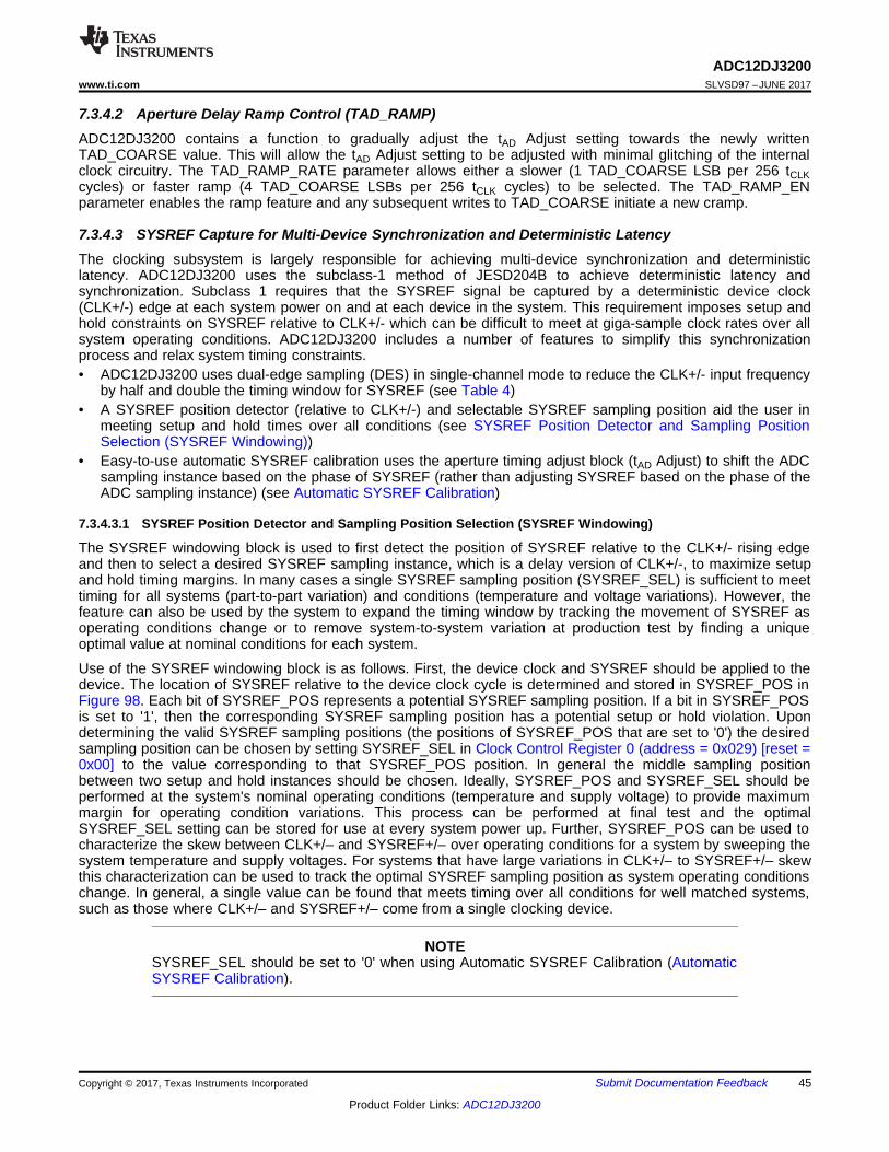
45
ADC12DJ3200www.ti.com SLVSD97 –JUNE 2017
Product Folder Links: ADC12DJ3200
Submit Documentation FeedbackCopyright © 2017, Texas Instruments Incorporated
7.3.4.2 Aperture Delay Ramp Control (TAD_RAMP)ADC12DJ3200 contains a function to gradually adjust the tAD Adjust setting towards the newly writtenTAD_COARSE value. This will allow the tAD Adjust setting to be adjusted with minimal glitching of the internalclock circuitry. The TAD_RAMP_RATE parameter allows either a slower (1 TAD_COARSE LSB per 256 tCLKcycles) or faster ramp (4 TAD_COARSE LSBs per 256 tCLK cycles) to be selected. The TAD_RAMP_ENparameter enables the ramp feature and any subsequent writes to TAD_COARSE initiate a new cramp.
7.3.4.3 SYSREF Capture for Multi-Device Synchronization and Deterministic LatencyThe clocking subsystem is largely responsible for achieving multi-device synchronization and deterministiclatency. ADC12DJ3200 uses the subclass-1 method of JESD204B to achieve deterministic latency andsynchronization. Subclass 1 requires that the SYSREF signal be captured by a deterministic device clock(CLK+/-) edge at each system power on and at each device in the system. This requirement imposes setup andhold constraints on SYSREF relative to CLK+/- which can be difficult to meet at giga-sample clock rates over allsystem operating conditions. ADC12DJ3200 includes a number of features to simplify this synchronizationprocess and relax system timing constraints.• ADC12DJ3200 uses dual-edge sampling (DES) in single-channel mode to reduce the CLK+/- input frequency
by half and double the timing window for SYSREF (see Table 4)• A SYSREF position detector (relative to CLK+/-) and selectable SYSREF sampling position aid the user in
meeting setup and hold times over all conditions (see SYSREF Position Detector and Sampling PositionSelection (SYSREF Windowing))
• Easy-to-use automatic SYSREF calibration uses the aperture timing adjust block (tAD Adjust) to shift the ADCsampling instance based on the phase of SYSREF (rather than adjusting SYSREF based on the phase of theADC sampling instance) (see Automatic SYSREF Calibration)
7.3.4.3.1 SYSREF Position Detector and Sampling Position Selection (SYSREF Windowing)
The SYSREF windowing block is used to first detect the position of SYSREF relative to the CLK+/- rising edgeand then to select a desired SYSREF sampling instance, which is a delay version of CLK+/-, to maximize setupand hold timing margins. In many cases a single SYSREF sampling position (SYSREF_SEL) is sufficient to meettiming for all systems (part-to-part variation) and conditions (temperature and voltage variations). However, thefeature can also be used by the system to expand the timing window by tracking the movement of SYSREF asoperating conditions change or to remove system-to-system variation at production test by finding a uniqueoptimal value at nominal conditions for each system.
Use of the SYSREF windowing block is as follows. First, the device clock and SYSREF should be applied to thedevice. The location of SYSREF relative to the device clock cycle is determined and stored in SYSREF_POS inFigure 98. Each bit of SYSREF_POS represents a potential SYSREF sampling position. If a bit in SYSREF_POSis set to '1', then the corresponding SYSREF sampling position has a potential setup or hold violation. Upondetermining the valid SYSREF sampling positions (the positions of SYSREF_POS that are set to '0') the desiredsampling position can be chosen by setting SYSREF_SEL in Clock Control Register 0 (address = 0x029) [reset =0x00] to the value corresponding to that SYSREF_POS position. In general the middle sampling positionbetween two setup and hold instances should be chosen. Ideally, SYSREF_POS and SYSREF_SEL should beperformed at the system's nominal operating conditions (temperature and supply voltage) to provide maximummargin for operating condition variations. This process can be performed at final test and the optimalSYSREF_SEL setting can be stored for use at every system power up. Further, SYSREF_POS can be used tocharacterize the skew between CLK+/– and SYSREF+/– over operating conditions for a system by sweeping thesystem temperature and supply voltages. For systems that have large variations in CLK+/– to SYSREF+/– skewthis characterization can be used to track the optimal SYSREF sampling position as system operating conditionschange. In general, a single value can be found that meets timing over all conditions for well matched systems,such as those where CLK+/– and SYSREF+/– come from a single clocking device.
NOTESYSREF_SEL should be set to '0' when using Automatic SYSREF Calibration (AutomaticSYSREF Calibration).

46
ADC12DJ3200SLVSD97 –JUNE 2017 www.ti.com
Product Folder Links: ADC12DJ3200
Submit Documentation Feedback Copyright © 2017, Texas Instruments Incorporated
The step size between each SYSREF_POS sampling position can be adjusted using SYSREF_ZOOM. WhenSYSREF_ZOOM is set to '0', the delay steps are more coarse. When SYSREF_ZOOM is set to '1', the delaysteps finer steps. See Switching Characteristics for delay step sizes when SYSREF_ZOOM is enabled anddisabled. In general, SYSREF_ZOOM should always be used (SYSREF_ZOOM = 1) unless a transition region(defined by 1's in SYSREF_POS) is not seen, such as could be the case for low clock rates. Bits 0 and 23 ofSYSREF_POS will always be set to '1' since it cannot be determined if these settings are close to a timingviolation, although the actual valid window could extend beyond these sampling positions. The valueprogrammed into SYSREF_SEL is the decimal number representing the desired bit location in SYSREF_POS.Table 6 shows some example SYSREF_POS readings and the optimal SYSREF_SEL settings. Although 24sampling positions are provided by the SYSREF_POS status register, SYSREF_SEL only allows selection of thefirst 16 sampling positions, corresponding to SYSREF_POS bits 0 to 15. The additional SYSREF_POS statusbits are intended only to provide additional knowledge of the SYSREF valid window. In general, lower values ofSYSREF_SEL should be selected due to variation of the delays over supply voltage, however in the fourthexample a value of 15 provides additional margin and may be selected instead.
Table 6. Examples of SYSREF_POS Readings and SYSREF_SEL SelectionsSYSREF_POS[23:0]
OPTIMAL SYSREF_SELSETTING0x02E[7:0]
(Largest Delay) 0x02D[7:0] 0x02C[7:0](Smallest Delay)
b10000000 b01100000 b00011001 8 or 9b10011000 b00000000 b00110001 12b10000000 b01100000 b00000001 6 or 7b10000000 b00000011 b00000001 4 or 15b10001100 b01100011 b00011001 6
7.3.4.3.2 Automatic SYSREF Calibration
ADC12DJ3200 has an automatic SYSREF calibration feature to alleviate the often challenging setup and holdtimes associated with capturing SYSREF for giga-sample data converters. Automatic SYSREF Calibration usesthe tAD Adjust feature to shift the device clock to maximize the SYSREF setup and hold times or align thesampling instance based on the SYSREF rising edge.
ADC12DJ3200 must have a proper device clock applied and be programmed for normal operation before startingAutomatic SYSREF Calibration. When ready to initiate Automatic SYSREF Calibration a continuous SYSREFsignal should be applied. Note that SYSREF must be a continuous (periodic) signal when using AutomaticSYSREF Calibration. Start the calibration process by setting SRC_EN high in Figure 173 after configuringAutomatic SYSREF Calibration using the SRC_CFG register. Upon setting SRC_EN high ADC12DJ3200searches for the optimal tAD Adjust setting until the device clock falling edge is internally aligned to the SYSREFrising edge. TAD_DONE in Figure 175 can be monitored to ensure that SYSREF calibration has finished. Byaligning the device clock falling edge with the SYSREF rising edge Automatic SYSREF Calibration maximizesthe internal SYSREF setup and hold times relative to the device clock while also setting the sampling instantbased on the SYSREF rising edge. After Automatic SYSREF Calibration finishes the rest of the startupprocedure can be performed to finish bringing up the system.
For multi-device synchronization the timing of the SYSREF rising edge should be matched at all devices andtherefore trace lengths should be matched from a common SYSREF source to each ADC12DJ3200. Any skewbetween the SYSREF rising edge at each device will result in additional error in the sampling instance betweendevices, however repeatable deterministic latency from system startup to startup through each device should stillbe achieved. No other design requirements are needed in order to achieve multi-device synchronization as longas a proper elastic buffer release point is chosen in the receiver.
A timing diagram of the SYSREF calibration procedure is shown in Figure 67. The optimized setup and holdtimes are shown as tSU(OPT) and tH(OPT), respectively. Device clock and SYSREF are referred to as "internal" inthis diagram since the phase of the internal signals are aligned within the device and not to the external (applied)phase of device clock or SYSREF.
Sampled Input
Signal
Internal Unadjusted
Device Clock
Internal SYSREF
SRC_EN
(SPI register bit)
tH(OPT) tSU(OPT)
Internal Calibrated
Device Clock
Before calibration, device clock falling edge
does not align with SYSREF rising edge
tTAD(SRC)
Calibration
enabled
After calibration, device clock falling
edge aligns with SYSREF rising edge
tCAL(SRC)
TAD_DONE
(SPI register bit) Calibration
finished
47
ADC12DJ3200www.ti.com SLVSD97 –JUNE 2017
Product Folder Links: ADC12DJ3200
Submit Documentation FeedbackCopyright © 2017, Texas Instruments Incorporated
Figure 67. SYSREF Calibration Timing Diagram
Once finished, the tAD Adjust setting found by Automatic SYSREF Calibration can be read from SRC_TAD inFigure 175. After calibration, the system will continue to use the calibrated tAD Adjust setting for operation untilthe system is powered down. However, if desired, the user can then disable SYSREF calibration and fine-tunethe tAD Adjust setting according to the systems needs. Alternatively, the use of Automatic SYSREF Calibrationcan be done at product test (or periodic re-calibration) of the optimal tAD Adjust setting for each system. Thisvalue can be stored and written to the TAD register (TAD_INV, TAD_COARSE and TAD_FINE) upon systemstartup.
SYSREF calibration should not be run while ADC calibration (foreground or background) is running. Ifbackground calibration is the desired use case, it should be disabled while SYSREF calibration is used, thenreenabled after TAD_DONE goes high. SYSREF_SEL in Clock Control Register 0 (address = 0x029) [reset =0x00] must be set to 0 when using SYSREF calibration.
SYSREF calibration will search the TAD_COARSE delays using both non-inverted (TAD_INV = 0) and invertedclock polarity (TAD_INV = 1) to minimize the required TAD_COARSE setting in order to minimize loss on theclock path to reduce aperture jitter (tAJ).
7.3.5 Digital Down Converters (Dual Channel Mode Only)After converting the analog voltage to a digital value, the digitized sample can either be sent directly to theJESD204B interface block (DDC bypass) or it can be sent to the digital down conversion (DDC) block forfrequency conversion and decimation (in dual channel mode only). Frequency conversion and decimation allow aspecific frequency band to be selected and output in the digital data stream while reducing the effective data rateand interface speed or width. The DDC is designed such that the digital processing does not degrade the noisespectral density (NSD) performance of the ADC. The digital down converter for channel A of the ADC12DJ3200is shown in Figure 68. Channel B has the same structure with the input data selected by DIG_BIND_B and theNCO selection mux controlled by pins NCOB[1:0] or through CSELB[1:0].
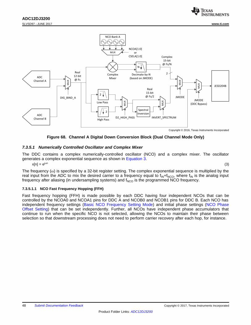
NCO Bank A
Complex
Mixer
N
MUX
NCOA[1:0]
or
CSELA[1:0]
2
Decimate-by-N
(based on JMODE)
Spectral
Inversion2
MU
X
High Pass
Low Pass
MU
X
MU
X
Real
12-bit
@ Fs
Complex
15-bit
@ Fs/N
2
Real
15-bit
@ Fs/2
MU
X
DIG_BIND_A
D2_HIGH_PASS INVERT_SPECTRUM
MU
X
JMODE
(DDC Bypass)
JMODE
ADC
Channel A
ADC
Channel B
JESD204B
Copyright © 2016, Texas Instruments Incorporated
48
ADC12DJ3200SLVSD97 –JUNE 2017 www.ti.com
Product Folder Links: ADC12DJ3200
Submit Documentation Feedback Copyright © 2017, Texas Instruments Incorporated
Figure 68. Channel A Digital Down Conversion Block (Dual Channel Mode Only)
7.3.5.1 Numerically Controlled Oscillator and Complex MixerThe DDC contains a complex numerically-controlled oscillator (NCO) and a complex mixer. The oscillatorgenerates a complex exponential sequence as shown in Equation 3.
x[n] = ejωn (3)
The frequency (ω) is specified by a 32-bit register setting. The complex exponential sequence is multiplied by thereal input from the ADC to mix the desired carrier to a frequency equal to fIN+fNCO, where fIN is the analog inputfrequency after aliasing (in undersampling systems) and fNCO is the programmed NCO frequency.
7.3.5.1.1 NCO Fast Frequency Hopping (FFH)
Fast frequency hopping (FFH) is made possible by each DDC having four independent NCOs that can becontrolled by the NCOA0 and NCOA1 pins for DDC A and NCOB0 and NCOB1 pins for DDC B. Each NCO hasindependent frequency settings (Basic NCO Frequency Setting Mode) and initial phase settings (NCO PhaseOffset Setting) that can be set independently. Further, all NCOs have independent phase accumulators thatcontinue to run when the specific NCO is not selected, allowing the NCOs to maintain their phase betweenselection so that downstream processing does not need to perform carrier recovery after each hop, for instance.

DDC BlockNCO Bank A
Complex
Mixer
N
MUXNCOx[1:0]
Decimate-by-N
(based on JMODE)
ADC JESD204B
tGPIO-MIXER
tMIXER-TX
Dx0+/-
Dx1+/-
Dx2+/-
Dx7+/-
INx+
INx-
tADC-MIXER
Copyright © 2016, Texas Instruments Incorporated
49
ADC12DJ3200www.ti.com SLVSD97 –JUNE 2017
Product Folder Links: ADC12DJ3200
Submit Documentation FeedbackCopyright © 2017, Texas Instruments Incorporated
Figure 69. NCO Fast Frequency Hopping Latency Diagram
NCO hopping occurs when the NCO GPIO pins change state. The pins are controlled asynchronously andtherefore synchronous switching is not possible. Associated latencies are demonstrated in Figure 69, where tTXand tADC are provided in Switching Characteristics. All latencies in Table 7 are approximations only.
Table 7. NCO Fast Frequency Hopping Latency DefinitionsLatency Parameter Value or Calculation Units
tGPIO-MIXER ~36 to ~40 tCLK cyclestADC-MIXER ~36 tCLK cyclestMIXER-TX (tTX + tADC) – tADC-MIXER tCLK cycles
7.3.5.1.2 NCO Selection
Within each channel's DDC, four different frequency and phase settings are available for use. Each of the foursettings uses a different phase accumulator within the NCO. Since all four phase accumulators are independentand continuously running, rapid switching between different NCO frequencies is possible allowing for phasecoherent frequency hopping.
The specific frequency-phase pair used for each channel is selected through the NCOA[1:0] or NCOB[1:0] inputpins when CMODE is set to 1. Alternatively, the selected NCO can be chosen through SPI by CSELA for DDC Aand CSELB for DDC B by setting CMODE to 0 (default). The logic table for NCO selection is provided in Table 8for both GPIO and SPI selection options.
Table 8. Logic Table for NCO Selection using GPIO or SPINCO Selection CMODE NCOx1 NCOx0 CSELx[1] CSELx[0]
NCO 0 using GPIO 1 0 0 X XNCO 1 using GPIO 1 0 1 X XNCO 2 using GPIO 1 1 0 X XNCO 3 using GPIO 1 1 1 X XNCO 0 using SPI 0 X X 0 0NCO 1 using SPI 0 X X 0 1NCO 2 using SPI 0 X X 1 0NCO 3 using SPI 0 X X 1 1

( )26FREQAx round 2 N / NCO_RDIV= ´
(NCO)
(STEP)
¦N
¦
( )32NCO DEVCLKFREQAx /round 2= ´ ¦ ¦
( )DEVCLK STEP/NCO _RDIV
64
¦ ¦=
50
ADC12DJ3200SLVSD97 –JUNE 2017 www.ti.com
Product Folder Links: ADC12DJ3200
Submit Documentation Feedback Copyright © 2017, Texas Instruments Incorporated
The frequency for each phase accumulator is programmed independently through the FREQAx, FREQBx (x=0 to3) and, optionally, NCO_RDIV register settings. The phase offset for each accumulator is programmedindependently through the PHASEAx and PHASEBx (x=0 to 3) register settings.
7.3.5.1.3 Basic NCO Frequency Setting Mode
In basic NCO frequency-setting mode (NCO_RDIV = 0x0000), the NCO frequency setting is set by the 32-bitregister value, FREQAx and FREQBx (x = 0 to 3). The NCO frequency for DDC A can be calculated usingEquation 4, where FREQAx can be replaced by FREQBx to calculate the NCO frequency for DDC B.
ƒ(NCO) = FREQAx × 2–32 × ƒ(DEVCLK) (x = 0 – 3) (4)
NOTEChanging the FREQAx and FREQBx register settings results in non-deterministic NCOphase. If deterministic phase is required the NCOs must be resynchronized. See NCOPhase Synchronization.
7.3.5.1.4 Rational NCO Frequency Setting Mode
In basic NCO frequency mode, the frequency step size is very small and many frequencies can be synthesized,but sometimes an application requires very specific frequencies that fall between two frequency steps. Forexample with ƒS equal to 2457.6 MHz and a desired ƒ(NCO) equal to 5.02 MHz the value for FREQAx is8773085.867. Truncating the fractional portion results in an ƒ(NCO) equal to 5.0199995 MHz, which is not thedesired frequency.
To produce the desired frequency, the NCO_RDIV parameter is used to force the phase accumulator to arrive atspecific frequencies without error. First, select a frequency step size (ƒ(STEP)) that is appropriate for the NCOfrequency steps required. The typical value of ƒ(STEP) is 10 kHz. Next, program the NCO_RDIV value accordingto Equation 5.
(5)
The result of Equation 5 must be an integer value. If the value is not an integer, adjust either of the parametersuntil the result is an integer value.
For example, select a value of 1920 for NCO_RDIV.
NOTENCO_RDIV values larger than 8192 can degrade the NCO SFDR performance and arenot recommended.
Now use Equation 6 to calculate the FREQAx register value.
(6)
Alternatively, the following equations can be used:
(7)
(8)
Table 9. Common NCO_RDIV Values (For 10-kHz Frequency Steps)ƒ(DEVCLK) (MHz) NCO_RDIV
3200 50003072 4800
2949.12 46082457.6 3840

51
ADC12DJ3200www.ti.com SLVSD97 –JUNE 2017
Product Folder Links: ADC12DJ3200
Submit Documentation FeedbackCopyright © 2017, Texas Instruments Incorporated
Table 9. Common NCO_RDIV Values (For 10-kHz Frequency Steps) (continued)ƒ(DEVCLK) (MHz) NCO_RDIV
1966.08 30721600 2500
1474.56 23041228.8 1920
7.3.5.1.5 NCO Phase Offset Setting
The NCO phase-offset setting for each NCO is set by the 16-bit register value PHASEAx and PHASEBx (wherex = 0 to 3). The value is left-justified into a 32-bit field and then added to the phase accumulator.
Use Equation 9 to calculate the phase offset in radians.Φ(rad) = PHASEA/Bx × 2–16 × 2 × π (x=0 to 3) (9)
7.3.5.1.6 NCO Phase Synchronization
The NCOs must be synchronized after setting or changing the value of FREQAx or FREQBx. NCOsynchronization is performed when the JESD204B link is initialized or by SYSREF, based on the settings ofNCO_SYNC_ILA and NCO_SYNC_NEXT. The procedures are given below for the JESD204B initializationprocedure and the SYSREF procedure for both DC coupled and AC coupled SYSREF signals.
NCO synchronization using JESD204B SYNC signal (SYNCSE or TMSTP+/–):1. Device must be programmed for normal operation2. Set NCO_SYNC_ILA to 13. Set JESD_EN to 04. Program FREQAx, FREQBx, PHASEAx and PHASEBx to the desired settings5. In JESD204B receiver (logic device) deassert SYNC signal by setting it high6. Set JESD_EN to 17. Assert SYNC signal by setting it low in JESD204B receiver to start CGS process8. After achieving CGS, deassert SYNC signal by setting it high at the same time for all ADCs that are to be
synchronized and verify that SYNC setup and hold times are met (specified in Timing Requirements)
NCO synchronization using SYSREF (DC coupled):1. Device must be programmed for normal operation2. Set JESD_EN to 1 to start JESD204B link (SYNC signal can respond as normal during CGS process)3. Program FREQAx, FREQBx, PHASEAx and PHASEBx to the desired settings4. Verify that SYSREF is disabled (held low)5. Arm NCO synchronization by setting NCO_SYNC_NEXT to 16. Issue a single SYSREF pulse to all ADCs to synchronize NCOs within all devices
NCO synchronization using SYSREF (AC coupled):1. Device must be programmed for normal operation2. Set JESD_EN to 1 to start JESD204B link (SYNC signal can respond as normal during CGS process)3. Program FREQAx, FREQBx, PHASEAx and PHASEBx to the desired settings4. Run SYSREF continuously5. Arm NCO synchronization by setting NCO_SYNC_NEXT to 1 at the same time at all ADCs by timing the
rising edge of SCLK for the last data bit (LSB) at the end of the SPI write so that it occurs after a SYSREFrising edge and early enough before the next SYSREF rising edge so that the trigger is armed before thenext SYSREF rising edge (long SYSREF period is recommended)
6. NCOs in all ADCs will be synchronized by the next SYSREF rising edge
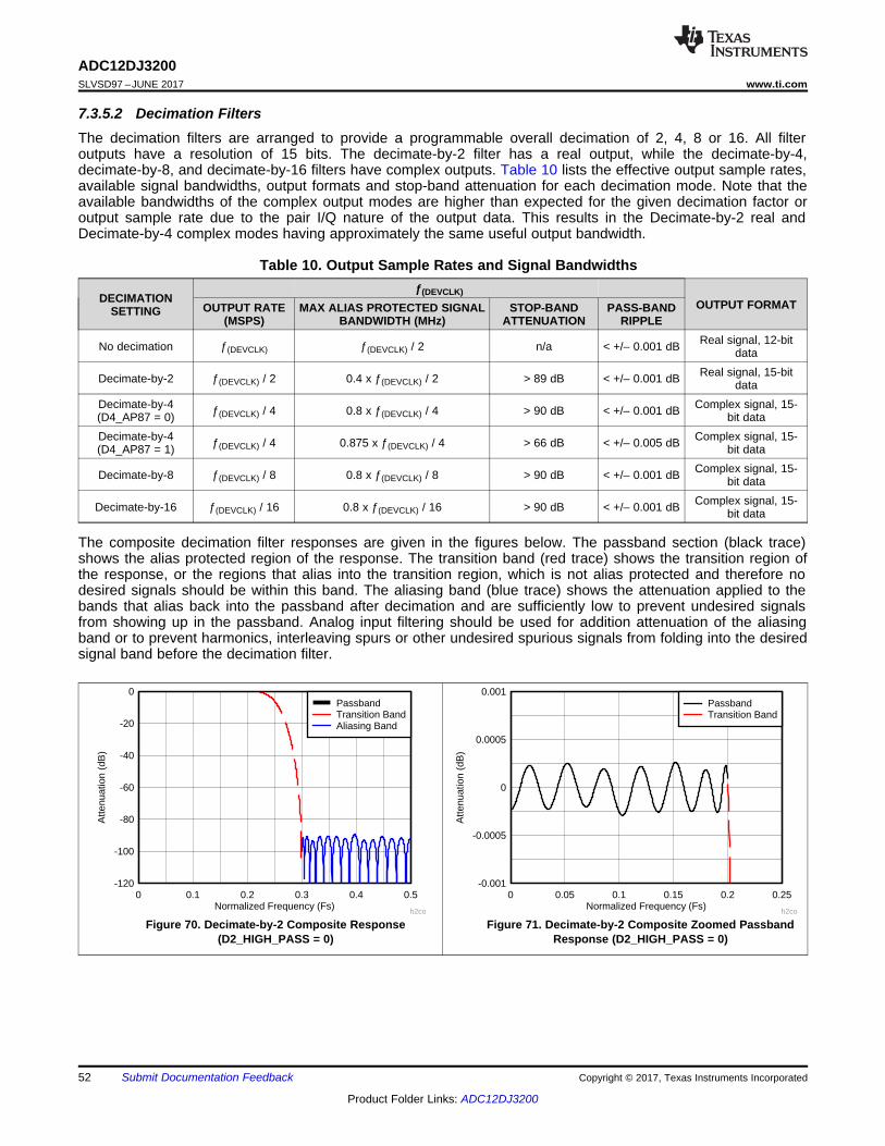
Normalized Frequency (Fs)
Atte
nuat
ion
(dB
)
0 0.1 0.2 0.3 0.4 0.5-120
-100
-80
-60
-40
-20
0
h2co
PassbandTransition BandAliasing Band
Normalized Frequency (Fs)
Atte
nuat
ion
(dB
)
0 0.05 0.1 0.15 0.2 0.25-0.001
-0.0005
0
0.0005
0.001
h2co
PassbandTransition Band
52
ADC12DJ3200SLVSD97 –JUNE 2017 www.ti.com
Product Folder Links: ADC12DJ3200
Submit Documentation Feedback Copyright © 2017, Texas Instruments Incorporated
7.3.5.2 Decimation FiltersThe decimation filters are arranged to provide a programmable overall decimation of 2, 4, 8 or 16. All filteroutputs have a resolution of 15 bits. The decimate-by-2 filter has a real output, while the decimate-by-4,decimate-by-8, and decimate-by-16 filters have complex outputs. Table 10 lists the effective output sample rates,available signal bandwidths, output formats and stop-band attenuation for each decimation mode. Note that theavailable bandwidths of the complex output modes are higher than expected for the given decimation factor oroutput sample rate due to the pair I/Q nature of the output data. This results in the Decimate-by-2 real andDecimate-by-4 complex modes having approximately the same useful output bandwidth.
Table 10. Output Sample Rates and Signal Bandwidths
DECIMATIONSETTING
ƒ(DEVCLK)OUTPUT FORMATOUTPUT RATE
(MSPS)MAX ALIAS PROTECTED SIGNAL
BANDWIDTH (MHz)STOP-BAND
ATTENUATIONPASS-BAND
RIPPLE
No decimation ƒ(DEVCLK) ƒ(DEVCLK) / 2 n/a < +/– 0.001 dB Real signal, 12-bitdata
Decimate-by-2 ƒ(DEVCLK) / 2 0.4 x ƒ(DEVCLK) / 2 > 89 dB < +/– 0.001 dB Real signal, 15-bitdata
Decimate-by-4(D4_AP87 = 0) ƒ(DEVCLK) / 4 0.8 x ƒ(DEVCLK) / 4 > 90 dB < +/– 0.001 dB Complex signal, 15-
bit dataDecimate-by-4(D4_AP87 = 1) ƒ(DEVCLK) / 4 0.875 x ƒ(DEVCLK) / 4 > 66 dB < +/– 0.005 dB Complex signal, 15-
bit data
Decimate-by-8 ƒ(DEVCLK) / 8 0.8 x ƒ(DEVCLK) / 8 > 90 dB < +/– 0.001 dB Complex signal, 15-bit data
Decimate-by-16 ƒ(DEVCLK) / 16 0.8 x ƒ(DEVCLK) / 16 > 90 dB < +/– 0.001 dB Complex signal, 15-bit data
The composite decimation filter responses are given in the figures below. The passband section (black trace)shows the alias protected region of the response. The transition band (red trace) shows the transition region ofthe response, or the regions that alias into the transition region, which is not alias protected and therefore nodesired signals should be within this band. The aliasing band (blue trace) shows the attenuation applied to thebands that alias back into the passband after decimation and are sufficiently low to prevent undesired signalsfrom showing up in the passband. Analog input filtering should be used for addition attenuation of the aliasingband or to prevent harmonics, interleaving spurs or other undesired spurious signals from folding into the desiredsignal band before the decimation filter.
Figure 70. Decimate-by-2 Composite Response(D2_HIGH_PASS = 0)
Figure 71. Decimate-by-2 Composite Zoomed PassbandResponse (D2_HIGH_PASS = 0)
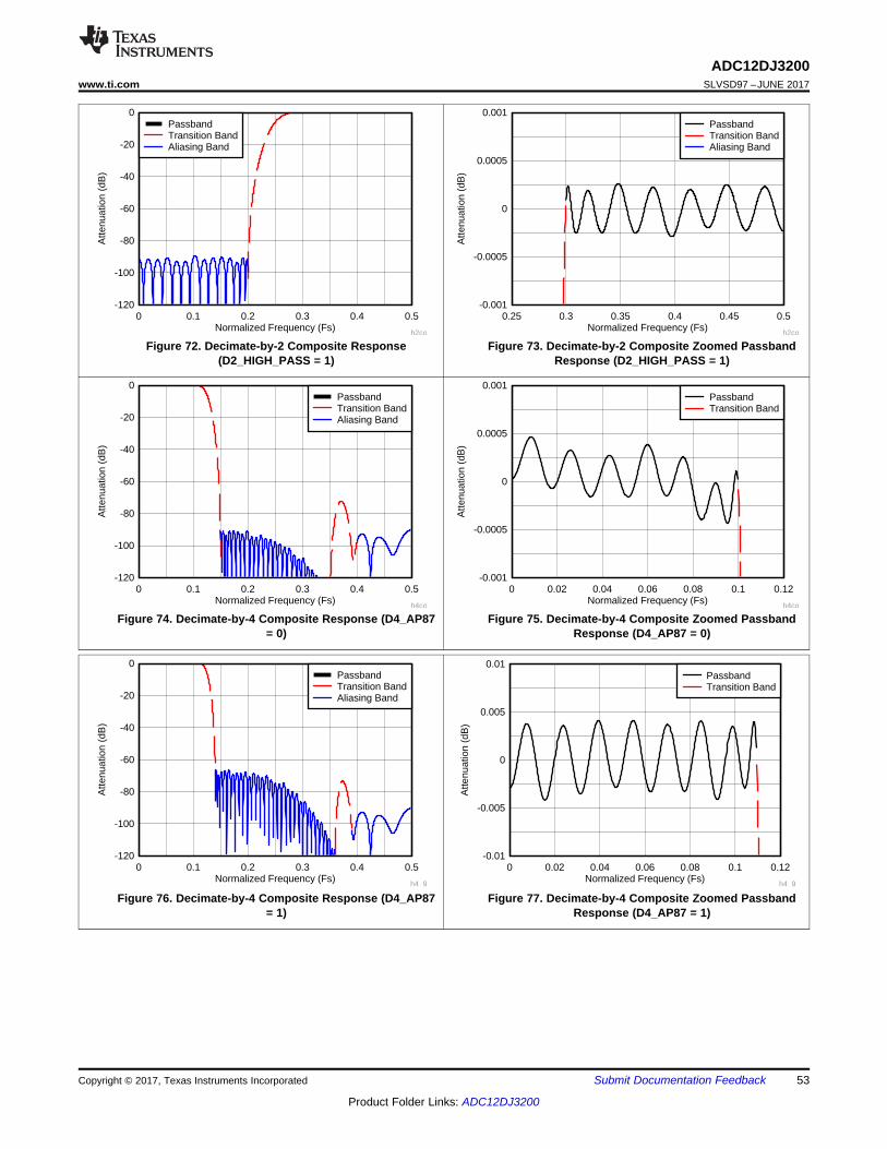
Normalized Frequency (Fs)
Atte
nuat
ion
(dB
)
0 0.1 0.2 0.3 0.4 0.5-120
-100
-80
-60
-40
-20
0
h4_9
PassbandTransition BandAliasing Band
Normalized Frequency (Fs)
Atte
nuat
ion
(dB
)
0 0.02 0.04 0.06 0.08 0.1 0.12-0.01
-0.005
0
0.005
0.01
h4_9
PassbandTransition Band
Normalized Frequency (Fs)
Atte
nuat
ion
(dB
)
0 0.1 0.2 0.3 0.4 0.5-120
-100
-80
-60
-40
-20
0
h4co
PassbandTransition BandAliasing Band
Normalized Frequency (Fs)
Atte
nuat
ion
(dB
)
0 0.02 0.04 0.06 0.08 0.1 0.12-0.001
-0.0005
0
0.0005
0.001
h4co
PassbandTransition Band
Normalized Frequency (Fs)
Atte
nuat
ion
(dB
)
0 0.1 0.2 0.3 0.4 0.5-120
-100
-80
-60
-40
-20
0
h2co
PassbandTransition BandAliasing Band
Normalized Frequency (Fs)
Atte
nuat
ion
(dB
)
0.25 0.3 0.35 0.4 0.45 0.5-0.001
-0.0005
0
0.0005
0.001
h2co
PassbandTransition BandAliasing Band
53
ADC12DJ3200www.ti.com SLVSD97 –JUNE 2017
Product Folder Links: ADC12DJ3200
Submit Documentation FeedbackCopyright © 2017, Texas Instruments Incorporated
Figure 72. Decimate-by-2 Composite Response(D2_HIGH_PASS = 1)
Figure 73. Decimate-by-2 Composite Zoomed PassbandResponse (D2_HIGH_PASS = 1)
Figure 74. Decimate-by-4 Composite Response (D4_AP87= 0)
Figure 75. Decimate-by-4 Composite Zoomed PassbandResponse (D4_AP87 = 0)
Figure 76. Decimate-by-4 Composite Response (D4_AP87= 1)
Figure 77. Decimate-by-4 Composite Zoomed PassbandResponse (D4_AP87 = 1)
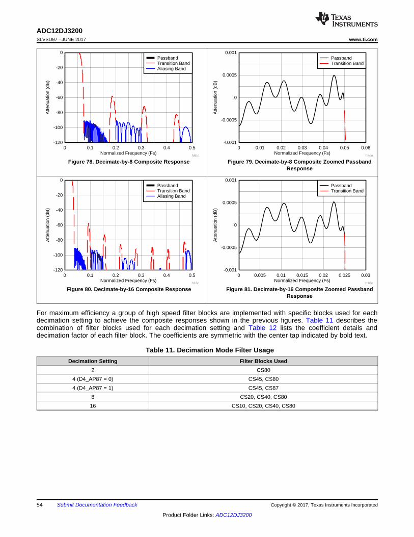
Normalized Frequency (Fs)
Atte
nuat
ion
(dB
)
0 0.1 0.2 0.3 0.4 0.5-120
-100
-80
-60
-40
-20
0
h16c
PassbandTransition BandAliasing Band
Normalized Frequency (Fs)
Atte
nuat
ion
(dB
)
0 0.005 0.01 0.015 0.02 0.025 0.03-0.001
-0.0005
0
0.0005
0.001
h16c
PassbandTransition Band
Normalized Frequency (Fs)
Atte
nuat
ion
(dB
)
0 0.1 0.2 0.3 0.4 0.5-120
-100
-80
-60
-40
-20
0
h8co
PassbandTransition BandAliasing Band
Normalized Frequency (Fs)
Atte
nuat
ion
(dB
)
0 0.01 0.02 0.03 0.04 0.05 0.06-0.001
-0.0005
0
0.0005
0.001
h8co
PassbandTransition Band
54
ADC12DJ3200SLVSD97 –JUNE 2017 www.ti.com
Product Folder Links: ADC12DJ3200
Submit Documentation Feedback Copyright © 2017, Texas Instruments Incorporated
Figure 78. Decimate-by-8 Composite Response Figure 79. Decimate-by-8 Composite Zoomed PassbandResponse
Figure 80. Decimate-by-16 Composite Response Figure 81. Decimate-by-16 Composite Zoomed PassbandResponse
For maximum efficiency a group of high speed filter blocks are implemented with specific blocks used for eachdecimation setting to achieve the composite responses shown in the previous figures. Table 11 describes thecombination of filter blocks used for each decimation setting and Table 12 lists the coefficient details anddecimation factor of each filter block. The coefficients are symmetric with the center tap indicated by bold text.
Table 11. Decimation Mode Filter UsageDecimation Setting Filter Blocks Used
2 CS804 (D4_AP87 = 0) CS45, CS804 (D4_AP87 = 1) CS45, CS87
8 CS20, CS40, CS8016 CS10, CS20, CS40, CS80

55
ADC12DJ3200www.ti.com SLVSD97 –JUNE 2017
Product Folder Links: ADC12DJ3200
Submit Documentation FeedbackCopyright © 2017, Texas Instruments Incorporated
Table 12. Filter Coefficient DetailsFilter Coefficient Set (Decimation Factor of Filter)
CS10 (2) CS20 (2) CS40 (2) CS45 (2) CS80 (2) CS87 (2)
–65 –65 109 109 –327 –327 56 56 –37 –37 –15 –15
0 0 0 0 0 0 0 0 0 0 0 0
577 577 –837 –837 2231 2231 –401 –401 118 118 23 23
1024 0 0 0 0 0 0 0 0 0 0
4824 4824 –8881 –8881 1596 1596 –291 –291 –40 –40
8192 0 0 0 0 0 0 0 0
39742 39742 –4979 –4979 612 612 64 64
65536 0 0 0 0 0 0
20113 20113 –1159 –1159 –97 –97
32768 0 0 0 0
2031 2031 142 142
0 0 0 0
–3356 –3356 –201 –201
0 0 0 0
5308 5308 279 279
0 0 0 0
–8140 –8140 –380 –380
0 0 0 0
12284 12284 513 513
0 0 0 0
–18628 –18628 –690 –690
0 0 0 0
29455 29455 939 939
0 0 0 0
–53191 –53191 –1313 –1313
0 0 0 0
166059 166059 1956 1956
262144 0 0
–3398 –3398
0 0
10404 10404
16384
7.3.5.3 Output Data FormatThe DDC output data varies depending on the selected JMODE. Real decimate-by-2 mode (JMODE 9) consistsof 15-bit real output data. Complex decimation modes (JMODE 10 to 16), except for JMODE 12, consist of 15–bitcomplex data plus the two over-range threshold-detection control bits. JMODE 12 output data consists of 12-bitcomplex data, but does not include the two over-range threshold-detection control bits which should instead bemonitored using the ORA0/1 and ORB0/1 output pins. The following table lists the data format:
Table 13. Real Decimation (JMODE 9) Output Sample Format
DDCCHANNEL
ODD/EVEN
SAMPLE
16-BIT OUTPUT WORD
15 14 13 12 11 10 9 8 7 6 5 4 3 2 1 0
A EVEN DDC A even numbered sample 15-bit output data OVR_T0
A ODD DDC A odd numbered sample 15-bit output data OVR_T1
B EVEN DDC B even numbered sample 15-bit output data OVR_T0
B ODD DDC B odd numbered sample 15-bit output data OVR_T1
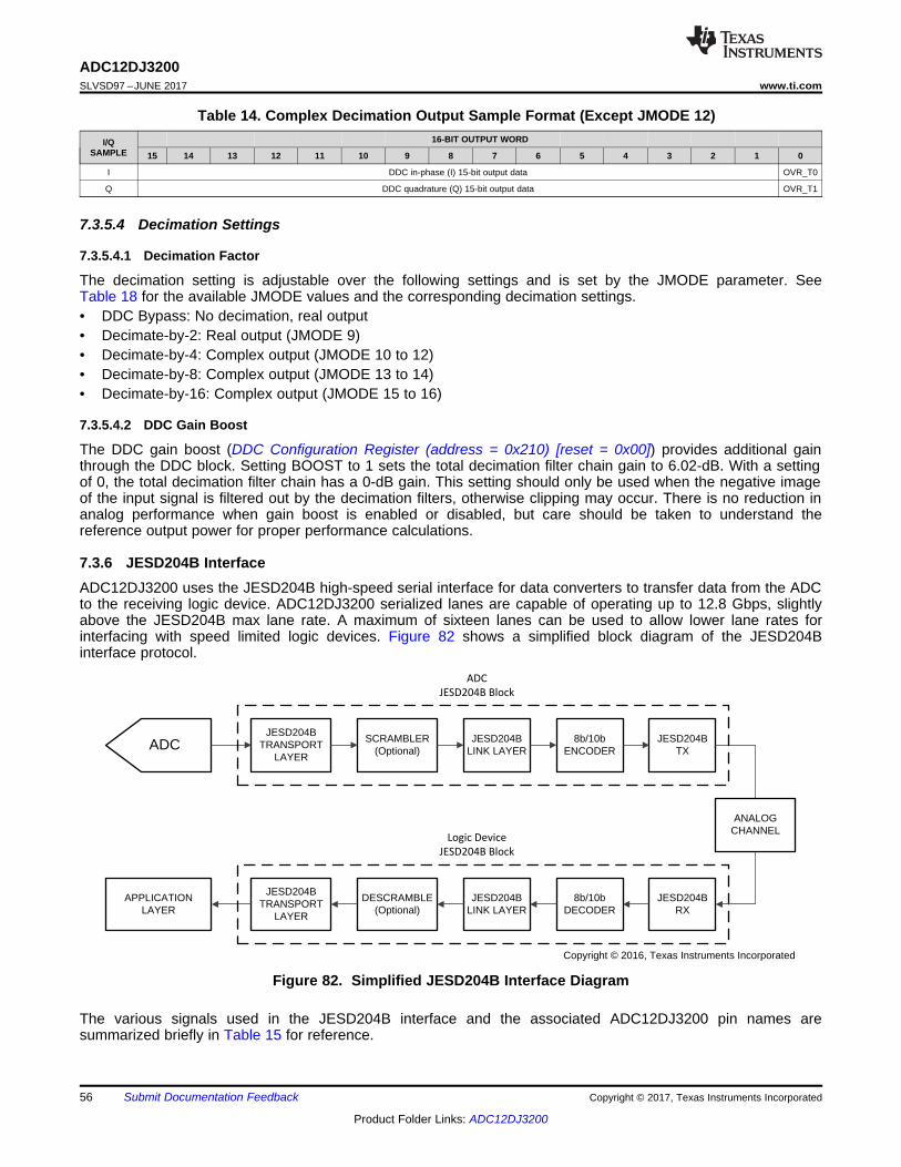
ADCJESD204B
TRANSPORT LAYER
SCRAMBLER(Optional)
JESD204BLINK LAYER
JESD204BTX
8b/10bENCODER
APPLICATION LAYER
JESD204BTRANSPORT
LAYER
DESCRAMBLE(Optional)
JESD204BLINK LAYER
JESD204BRX
8b/10bDECODER
ADC
JESD204B Block
Logic Device
JESD204B Block
ANALOGCHANNEL
Copyright © 2016, Texas Instruments Incorporated
56
ADC12DJ3200SLVSD97 –JUNE 2017 www.ti.com
Product Folder Links: ADC12DJ3200
Submit Documentation Feedback Copyright © 2017, Texas Instruments Incorporated
Table 14. Complex Decimation Output Sample Format (Except JMODE 12)I/Q
SAMPLE16-BIT OUTPUT WORD
15 14 13 12 11 10 9 8 7 6 5 4 3 2 1 0
I DDC in-phase (I) 15-bit output data OVR_T0
Q DDC quadrature (Q) 15-bit output data OVR_T1
7.3.5.4 Decimation Settings
7.3.5.4.1 Decimation Factor
The decimation setting is adjustable over the following settings and is set by the JMODE parameter. SeeTable 18 for the available JMODE values and the corresponding decimation settings.• DDC Bypass: No decimation, real output• Decimate-by-2: Real output (JMODE 9)• Decimate-by-4: Complex output (JMODE 10 to 12)• Decimate-by-8: Complex output (JMODE 13 to 14)• Decimate-by-16: Complex output (JMODE 15 to 16)
7.3.5.4.2 DDC Gain Boost
The DDC gain boost (DDC Configuration Register (address = 0x210) [reset = 0x00]) provides additional gainthrough the DDC block. Setting BOOST to 1 sets the total decimation filter chain gain to 6.02-dB. With a settingof 0, the total decimation filter chain has a 0-dB gain. This setting should only be used when the negative imageof the input signal is filtered out by the decimation filters, otherwise clipping may occur. There is no reduction inanalog performance when gain boost is enabled or disabled, but care should be taken to understand thereference output power for proper performance calculations.
7.3.6 JESD204B InterfaceADC12DJ3200 uses the JESD204B high-speed serial interface for data converters to transfer data from the ADCto the receiving logic device. ADC12DJ3200 serialized lanes are capable of operating up to 12.8 Gbps, slightlyabove the JESD204B max lane rate. A maximum of sixteen lanes can be used to allow lower lane rates forinterfacing with speed limited logic devices. Figure 82 shows a simplified block diagram of the JESD204Binterface protocol.
Figure 82. Simplified JESD204B Interface Diagram
The various signals used in the JESD204B interface and the associated ADC12DJ3200 pin names aresummarized briefly in Table 15 for reference.

57
ADC12DJ3200www.ti.com SLVSD97 –JUNE 2017
Product Folder Links: ADC12DJ3200
Submit Documentation FeedbackCopyright © 2017, Texas Instruments Incorporated
Table 15. Summary of JESD204B SignalsSignal Name ADC12DJ3200 Pin Names Description
Data DA0+...DA7+, DA0–...DA7–, DB0+...DB7+, DB0–...DB7– High-speed serialized data after8b/10b encoding
SYNC SYNCSE, TMSTP+, TMSTP–Link initialization signal (handshake),toggles low to start code groupsynchronization (CGS) process
Device Clock CLK+, CLK–ADC sampling clock, also used forclocking digital logic and outputserializers
SYSREF SYSREF+, SYSREF–
System timing reference used todeterministically reset the internal localmultiframe counters in eachJESD204B device
7.3.6.1 Transport LayerThe transport layer takes samples from the ADC output (in decimation bypass mode) or from the DDC outputand maps the samples into octets, frames, multiframes and lanes. Sample mapping is defined by the JESD204Bmode that is used, defined by parameters such as L, M, F, S, N, N', CF, etc. There are a number of predefinedtransport layer modes in the ADC12DJ3200 which are defined in Table 18. The high level configurationparameters for the transport layer in ADC12DJ3200 are described in Table 16. For simplicity, the transport layermode is chosen by simply setting the JMODE parameter and the desired K value. For reference, the variousconfiguration parameters for JESD204B are defined in Table 17.
7.3.6.2 ScramblerAn optional data scrambler can be used to scramble the octets before transmission across the channel.Scrambling is recommended in order to remove the possibility of spectral peaks in the transmitted data. TheJESD204B receiver automatically synchronizes its descrambler to the incoming scrambled data stream. Theinitial lane alignment sequence (ILA) is never scrambled. Scrambling can be enabled by setting SCR (JESD204BControl Register (address = 0x204) [reset = 0x02]).
7.3.6.3 Link LayerThe link layer serves multiple purposes in JESD204B, including establishing the code boundaries (Code GroupSynchronization (CGS)), initializing the link (Initial Lane Alignment Sequence (ILAS)), encoding the data (8b/10bEncoding) and monitoring the health of the link (Frame and Multiframe Monitoring).
7.3.6.3.1 Code Group Synchronization (CGS)
The first step in initializing the JESD204B link, after SYSREF is processed, is to achieve code groupsynchronization. The receiver first asserts the SYNC signal when ready to initialize the link. The transmitterresponds to the request by sending a stream of K28.5 characters. The receiver then aligns its character clock tothe K28.5 character sequence. Code group synchronization is achieved after receiving four K28.5 characterssuccessfully. The receiver deasserts SYNC on the next local multi-frame clock (LMFC) edge after CGS isachieved and waits for the transmitter to start the initial lane alignment sequence.
7.3.6.3.2 Initial Lane Alignment Sequence (ILAS)
After the transmitter sees the SYNC signal deassert it waits until its next LMFC edge to start sending the initiallane alignment sequence. The ILAS consists of four multiframes each containing a predetermined sequence. Thereceiver looks for the start of the ILAS to determine the frame and multiframe boundaries. As the ILAS reachesthe receiver for each lane, the lane starts to buffer its data until all receivers have received the ILAS andsubsequently release the ILAS from all lanes at the same time in order to align the lanes. The second multiframeof the ILAS contains configuration parameters for the JESD204B that can be used by the receiver to verify thatthe transmitter and receiver configurations match.
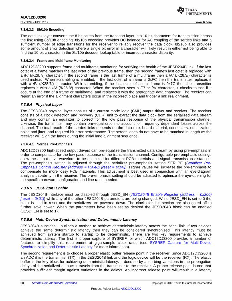
58
ADC12DJ3200SLVSD97 –JUNE 2017 www.ti.com
Product Folder Links: ADC12DJ3200
Submit Documentation Feedback Copyright © 2017, Texas Instruments Incorporated
7.3.6.3.3 8b/10b Encoding
The data link layer converts the 8-bit octets from the transport layer into 10-bit characters for transmission acrossthe link using 8b/10b encoding. 8b/10b encoding provides DC balance for AC coupling of the serdes links and asufficient number of edge transitions for the receiver to reliably recover the data clock. 8b/10b also providessome amount of error detection where a single bit error in a character will likely result in either not being able tofind the 10-bit character in the 8b/10b decoder lookup table or incorrect character disparity.
7.3.6.3.4 Frame and Multiframe Monitoring
ADC12DJ3200 supports frame and multiframe monitoring for verifying the health of the JESD204B link. If the lastoctet of a frame matches the last octet of the previous frame, then the second frame's last octet is replaced witha /F/ (/K28.7/) character. If the second frame is the last frame of a multiframe then a /A/ (/K28.3/) character isused instead. When scrambling is enabled, if the last octet of a frame is 0xFC then the transmitter replaces itwith a /F/ (/K28.7/) character. With scrambling, if the last octet of a multiframe is 0x7C then the transmitterreplaces it with a /A/ (/K28.3/) character. When the receiver sees a /F/ or /A/ character, it checks to see if itoccurs at the end of a frame or multiframe, and replaces it with the appropriate data character. The receiver canreport an error if the alignment characters occur in the incorrect place and trigger a link realignment.
7.3.6.4 Physical LayerThe JESD204B physical layer consists of a current mode logic (CML) output driver and receiver. The receiverconsists of a clock detection and recovery (CDR) unit to extract the data clock from the serialized data streamand may contain an equalizer to correct for the low pass response of the physical transmission channel.Likewise, the transmitter may contain pre-equalization to account for frequency dependent losses across thechannel. The total reach of the serdes links depends on the data rate, board material, connectors, equalization,noise and jitter, and required bit-error performance. The serdes lanes do not have to be matched in length as thereceiver will align the lanes during the initial lane alignment sequence.
7.3.6.4.1 Serdes Pre-Emphasis
ADC12DJ3200 high-speed output drivers can pre-equalize the transmitted data stream by using pre-emphasis inorder to compensate for the low pass response of the transmission channel. Configurable pre-emphasis settingsallow the output drive waveform to be optimized for different PCB materials and signal transmission distances.The pre-emphasis setting is adjusted through the serializer pre-emphasis setting SER_PE (Serializer Pre-Emphasis Control Register (address = 0x048) [reset = 0x00]). Higher values will increase the pre-emphasis tocompensate for more lossy PCB materials. This adjustment is best used in conjunction with an eye-diagramanalysis capability in the receiver. The pre-emphasis setting should be adjusted to optimize the eye-opening forthe specific hardware configuration and line rates needed.
7.3.6.5 JESD204B EnableThe JESD204B interface must be disabled through JESD_EN (JESD204B Enable Register (address = 0x200)[reset = 0x01]) while any of the other JESD204B parameters are being changed. While JESD_EN is set to 0 theblock is held in reset and the serializers are powered down. The clocks for this section are also gated off tofurther save power. When the parameters have been set as desired the JESD204B block can be enabled(JESD_EN is set to 1).
7.3.6.6 Multi-Device Synchronization and Deterministic LatencyJESD204B subclass 1 outlines a method to achieve deterministic latency across the serial link. If two devicesachieve the same deterministic latency then they can be considered synchronized. This latency must beachieved from system startup to startup to be deterministic. There are two key requirements to achievedeterministic latency. The first is proper capture of SYSREF for which ADC12DJ3200 provides a number offeatures to simplify this requirement at giga-sample clock rates (see SYSREF Capture for Multi-DeviceSynchronization and Deterministic Latency for more information).
The second requirement is to choose a proper elastic buffer release point in the receiver. Since ADC12DJ3200 isan ADC it is the transmitter (TX) in the JESD204B link and the logic device will be the receiver (RX). The elasticbuffer is the key block for achieving deterministic latency. It does so by absorbing variations in the propagationdelays of the serialized data as it travels from the transmitter to the receiver. A proper release point is one thatprovides sufficient margin against variations in the delays. An incorrect release point will result in a latency
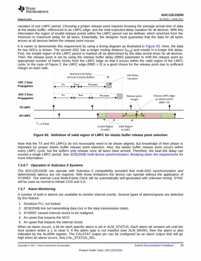
TX LMFC
RX LMFC
ADC 1 Data
PropagationtTX tPCB tRX-DESER
Time
ADC 2 Data
Propagation
tTX tPCB
Invalid Region
of LMFC
Valid Region
of LMFC
Nominal Link Delay
(Arrival at Elastic Buffer)Link Delay
Variation
Choose LMFC edge
as release point
(RBD = 0)
Release point
margin
tRX-DESER
59
ADC12DJ3200www.ti.com SLVSD97 –JUNE 2017
Product Folder Links: ADC12DJ3200
Submit Documentation FeedbackCopyright © 2017, Texas Instruments Incorporated
variation of one LMFC period. Choosing a proper release point requires knowing the average arrival time of dataat the elastic buffer, referenced to an LMFC edge, and the total expected delay variation for all devices. With thisinformation the region of invalid release points within the LMFC period can be defined, which stretches from theminimum to maximum delay for all lanes. Essentially, the designer must guarantee that the data for all lanesarrives at all devices before the release point occurs.
It is easier to demonstrate this requirement by using a timing diagram as illustrated in Figure 83. Here, the datafor two ADCs is shown. The second ADC has a longer routing distance (tPCB) and results in a longer link delay.First, the invalid region of the LMFC period is marked off as determined by the data arrival times for all devices.Then, the release point is set by using the release buffer delay (RBD) parameter to shift the release point anappropriate number of frame clocks from the LMFC edge so that it occurs within the valid region of the LMFCcycle. In the case of Figure 2, the LMFC edge (RBD = 0) is a good choice for the release point due to sufficientmargin on each side.
Figure 83. Definition of valid region of LMFC for elastic buffer release point selection
Note that the TX and RX LMFCs do not necessarily need to be phase aligned, but knowledge of their phase isimportant for proper elastic buffer release point selection. Also, the elastic buffer release point occurs withinevery LMFC cycle, but the buffers only release once all lanes have arrived. Therefore, the total link delay canexceed a single LMFC period. See JESD204B multi-device synchronization: Breaking down the requirements formore information.
7.3.6.7 Operation in Subclass 0 SystemsThe ADC12DJ3200 can operate with Subclass 0 compatibility provided that multi-ADC synchronization anddeterministic latency are not required. With those limitations the device can operate without the application ofSYSREF. The internal Local Multi-Frame Clock will be automatically self-generated with unknown timing. SYNCwill be used as normal to initiate CGS and ILA.
7.3.7 Alarm MonitoringA number of built in alarms are available to monitor internal events. Several types of alarms/upsets are detectedby this feature:
1. Serializer PLL not locked2. JESD204B link not transmitting data (not in the data transmission state)3. SYSREF caused internal clocks to be realigned4. An upset that impacts the NCO5. An upset that impacts the internal clocks
When an alarm occurs, a bit for each specific alarm is set in ALM_STATUS. Each alarm bit remains set until thehost system writes a 1 to clear it. If the alarm type is not masked (see ALM_MASK), then the alarm is alsoindicated by the ALARM register. The CALSTAT output pin can be configured as an alarm output that will gohigh when an alarm occurs. See CAL_STATUS_SEL.

60
ADC12DJ3200SLVSD97 –JUNE 2017 www.ti.com
Product Folder Links: ADC12DJ3200
Submit Documentation Feedback Copyright © 2017, Texas Instruments Incorporated
7.3.7.1 NCO Upset DetectionThe NCO_ALM register bit indicates if the NCO in channel A or B may have been upset. The NCO phaseaccumulators in channel A are continuously compared to channel B. If they differ for even one clock cycle, theNCO_ALM register bit is set and remains set until cleared by the host system by writing a 1. This featurerequires the phase and frequency words for each NCO accumulator in DDC A (PHASEAx, FREQAx) to be set tothe same values as the NCO accumulators in DDC B (PHASEBx, FREQBx). For example, PHASEA0 must bethe same as PHASEB0 and FREQA0 must be the same as FREQB0, however PHASEA1 can be set to adifferent value than PHASEA0. This ultimate reduces the number of NCO frequencies available for phasecoherent frequency hopping from four to two for each DDC. Note that DDC B can use a different NCO frequencythan DDC A by setting the NCOB[1:0] pins to a different value than NCOA[1:0]. This detection is only valid afterthe NCOs have been synchronized by either SYSREF or the start of the ILA sequence (as determined byNCO_SYNC). For NCO upset detection to work properly, follow this usage model:
1. Program JESD_EN=02. Ensure the part is configured to utilize both channels (PD_ACH=0, PD_BCH=0)3. Select a JMODE that utilizes the NCO4. Program all NCO frequencies and phases the same for channel A and B, for example FREQA0=FREQB0,
FREQA1=FREQB1, FREQA2=FREQB2, FREQA3=FREQB3).5. If desired, utilize the CMODE and CSEL registers or the NCOA[1:0] and NCOB[1:0] pins to choose a unique
frequency for channel A and channel B6. Program JESD_EN=17. Synchronize the NCOs (using the ILA or using SYSREF). See NCO_SYNC register.8. Write a ‘1’ to the NCO_ALM register bit to clear it9. Monitor the NCO_ALM status bit or the CALSTAT output pin if CAL_STATUS_SEL is properly configured10. If the frequency or phase registers are changed while the NCO is enabled, the NCOs can get out of
synchronization. Repeat steps 7-9.11. If the device enters and exits global power down, repeat steps 7-9.
7.3.7.2 Clock Upset DetectionThe CLK_ALM register bit indicates if the internal clocks may have been upset. The clocks in channel A arecontinuously compared to channel B. If they differ for even one DEVCLK/2 cycle, the CLK_ALM register bit is setand remains set until cleared by the host system by writing a ‘1’. For the CLK_ALM register bit to functionproperly, follow this usage model:
1. Program JESD_EN=02. Ensure the part is configured to utilize both channels (PD_ACH=0, PD_BCH=0)3. Program JESD_EN=14. Write CLK_ALM=1 to clear CLK_ALM5. Monitor the CLK_ALM status bit or the CALSTAT output pin if CAL_STATUS_SEL is properly configured6. When exiting global power-down (via MODE or the PD pin), the CLK_ALM status bit may be set and should
be cleared by writing a '1' to CLK_ALM
7.3.8 Temperature Monitoring DiodeA built-in thermal monitoring diode is made available on the TDIODE+ and TDIODE– pins. This diode facilitatestemperature monitoring and characterization of the device in higher ambient temperature environments. Whilethe on-chip diode is not highly characterized, the diode can be used effectively by performing a baselinemeasurement (offset) at a known ambient or board temperature and creating a linear equation with the diodevoltage slope provided in Electrical Characteristics - DC Specifications. Offset measurement should be done withthe device unpowered or with the PD pin asserted to minimize device self-heating. PD pin should be assertedonly long enough to take the offset measurement. Recommended monitoring ICs include the LM95233 deviceand similar remote-diode temperature monitoring products from Texas Instruments.

61
ADC12DJ3200www.ti.com SLVSD97 –JUNE 2017
Product Folder Links: ADC12DJ3200
Submit Documentation FeedbackCopyright © 2017, Texas Instruments Incorporated
7.3.9 Analog Reference VoltageThe reference voltage for ADC12DJ3200 is derived from an internal bandgap reference. A buffered version of thereference voltage is available at the BG pin for user convenience. This output has an output-current capability of±100 μA. The BG output must be buffered if more current is required. No provision exists for the use of anexternal reference voltage, but the full-scale input voltage can be adjusted through the full-scale-range registersettings. In unique cases, the VA11 supply voltage can act as the reference voltage by setting BG_BYPASS(Internal Reference Bypass Register (address = 0x038) [reset = 0x00]).
7.4 Device Functional ModesADC12DJ3200 can be configured to operate in a number of functional modes. These modes are described in thissection.
7.4.1 Dual Channel ModeADC12DJ3200 can be used as a dual channel ADC where the sampling rate is equal to the clock frequency (FS= FCLK) provided at the CLK+ and CLK- pins. The two inputs, AIN+/- and BIN+/-, serve as the respective inputsfor each channel in this mode. This mode is chosen simply by setting JMODE to the appropriate setting for thedesired configuration as described in Table 18. The analog inputs can be swapped by setting DUAL_INPUT(Input Mux Control Register (address = 0x060) [reset = 0x01])
7.4.2 Single Channel Mode (DES Mode)ADC12DJ3200 can also be used as a single channel ADC where the sampling rate is equal to two times theclock frequency (FS = 2xFCLK) provided at the CLK+ and CLK– pins. This mode effectively interleaves the twoADC channels together to form a single channel ADC at twice the sampling rate. This mode is chosen simply bysetting JMODE to the appropriate setting for the desired configuration as described in Table 18. Either analoginput, INA+/– or INB+/–, can serve as the input to the ADC, however INA+/– is recommended for bestperformance. The analog input can be selected using SINGLE_INPUT (Input Mux Control Register (address =0x060) [reset = 0x01]). The digital down-converters cannot be used in single channel mode.
NOTEIn single channel mode it is strongly recommended that INA+/– be used as the input to theADC for optimized performance.
7.4.3 JESD204B ModesADC12DJ3200 can be programmed as a single channel or dual channel ADC, with or without decimation, and anumber JESD204B output formats. Table 16 summarizes the basic operating mode configuration parametersand whether they are user configured or derived.
NOTEPower down of the high speed data outputs (DA0+/– ... DA7+/–, DB0+/– ... DB7+/–) forextended times may reduce performance of the output serializers, especially at high datarates. Please see note beneath Recommended Operating Conditions for more information.
Table 16. ADC12DJ3200 Operating Mode Configuration ParametersParameter Description User configured or Derived ValueJMODE JESD204B operating mode,
automatically derives the rest ofthe JESD204B parameters,single channel or dual channelmode and the decimation factor
User Set by JMODE (JESD204B ModeRegister (address = 0x201) [reset= 0x02])
D Decimation factor Derived See Table 18DES 1 = single channel mode, 0 =
dual channel modeDerived See Table 18
62
ADC12DJ3200SLVSD97 –JUNE 2017 www.ti.com
Product Folder Links: ADC12DJ3200
Submit Documentation Feedback Copyright © 2017, Texas Instruments Incorporated
Device Functional Modes (continued)Table 16. ADC12DJ3200 Operating Mode Configuration Parameters (continued)
Parameter Description User configured or Derived ValueR Number of bits transmitted per
lane per DEVCLK cycle. TheJESD204B linerate is theDEVCLK frequency times R. Thisparameter sets the SERDES PLLmultiplication factor or controlsbypassing of the SERDES PLL.
Derived See Table 18
Links Number of JESD204B links used Derived See Table 18K Number of frames per multi-
frameUser Configured Set by KM1 (JESD204B K
Parameter Register (address =0x202) [reset = 0x1F]), seeallowed values in Table 18
There are a number of parameters required to define the JESD204B format, all of which are sent across the linkduring the initial lane alignment sequence. In the ADC12DJ3200, most of the parameters are automaticallyderived based on the selected JMODE; however, a few are configured by the user. These parameters aredescribed in Table 17.
Table 17. JESD204B Initial Lane Alignment Sequence ParametersParameter Description User configured or Derived ValueADJCNT LMFC adjustment amount (not
applicable)Derived Always 0
ADJDIR LMFC adjustment direction (notapplicable)
Derived Always 0
BID Bank ID Derived Always 0CF Number of control words per
frameDerived Always 0
CS Control bits per sample Derived Always set to 0 in ILAS, seeTable 18 for actual usage
DID Device identifier, used to identifythe link
User Set by DID (JESD204B DIDParameter Register (address =0x206) [reset = 0x00]), seeTable 19
F Number of octets (bytes) perframe (per lane)
Derived See Table 18
HD High density format (samplessplit between lanes)
Derived Always 0
JESDV JESD204 standard revision Derived Always 1K Number of frames per multi-
frameUser Set by KM1 register, JESD204B
K Parameter Register (address =0x202) [reset = 0x1F]
L Number of serial output lanes perlink
Derived See Table 18
LID Lane identifier for each lane Derived See Table 19M Number of converters used to
determine lane bit packing; maynot match number of ADCchannels in the device
Derived See Table 18
N Sample resolution (before addingcontrol and tail bits)
Derived See Table 18
N' Bits per sample after addingcontrol and tail bits
Derived See Table 18
S Number of samples per converter(M) per frame
Derived See Table 18
SCR Scrambler enabled User Set by SCR register
63
ADC12DJ3200www.ti.com SLVSD97 –JUNE 2017
Product Folder Links: ADC12DJ3200
Submit Documentation FeedbackCopyright © 2017, Texas Instruments Incorporated
Table 17. JESD204B Initial Lane Alignment Sequence Parameters (continued)Parameter Description User configured or Derived ValueSUBCLASSV Device subclass version Derived Always 1RES1 Reserved field 1 Derived Always 0RES2 Reserved field 2 Derived Always 0CHKSUM Checksum for ILAS checking
(sum of all above parametersmodulo 256)
Derived Computed based on aboveparameters
Configuring the ADC12DJ3200 is made easy by use of a single configuration parameter called JMODE(JESD204B Mode Register (address = 0x201) [reset = 0x02]). Using Table 18, the correct JMODE value can befound for the desired operating mode. The modes shown in Table 18 are the only available operating modes.The table also gives a range and allowable step size for the K parameter (set by KM1, see JESD204B KParameter Register (address = 0x202) [reset = 0x1F]), which sets the multi-frame length in number of frames.
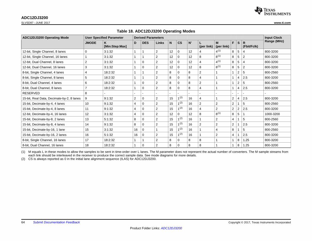
ADC12DJ3200SLVSD97 –JUNE 2017 www.ti.com
64
Product Folder Links: ADC12DJ3200
Submit Documentation Feedback Copyright © 2017, Texas Instruments Incorporated
(1) M equals L in these modes to allow the samples to be sent in time-order over L lanes. The M parameter does not represent the actual number of converters. The M sample streams fromeach link should be interleaved in the receiver to produce the correct sample data. See mode diagrams for more details.
(2) CS is always reported as 0 in the initial lane alignment sequence (ILAS) for ADC12DJ3200.
Table 18. ADC12DJ3200 Operating ModesADC12DJ3200 Operating Mode User Specified Parameter Derived Parameters Input Clock
Range (MHz)JMODE K[Min:Step:Max]
D DES Links N CS N’ L(per link)
M(per link)
F S R(Fbit/Fclk)
12-bit, Single Channel, 8 lanes 0 3:1:32 1 1 2 12 0 12 4 4 (1) 8 5 4 800-320012-bit, Single Channel, 16 lanes 1 3:1:32 1 1 2 12 0 12 8 8 (1) 8 5 2 800-320012-bit, Dual Channel, 8 lanes 2 3:1:32 1 0 2 12 0 12 4 4 (1) 8 5 4 800-320012-bit, Dual Channel, 16 lanes 3 3:1:32 1 0 2 12 0 12 8 8 (1) 8 5 2 800-32008-bit, Single Channel, 4 lanes 4 18:2:32 1 1 2 8 0 8 2 1 1 2 5 800-25608-bit, Single Channel, 8 lanes 5 18:2:32 1 1 2 8 0 8 4 1 1 4 2.5 800-32008-bit, Dual Channel, 4 lanes 6 18:2:32 1 0 2 8 0 8 2 1 1 2 5 800-25608-bit, Dual Channel, 8 lanes 7 18:2:32 1 0 2 8 0 8 4 1 1 4 2.5 800-3200RESERVED 8 - - - - - - - - - - - - -15-bit, Real Data, Decimate-by-2, 8 lanes 9 9:1:32 2 0 2 15 1 (2) 16 4 1 2 4 2.5 800-320015-bit, Decimate-by-4, 4 lanes 10 9:1:32 4 0 2 15 1 (2) 16 2 2 2 1 5 800-256015-bit, Decimate-by-4, 8 lanes 11 9:1:32 4 0 2 15 1 (2) 16 4 2 2 2 2.5 800-320012-bit, Decimate-by-4, 16 lanes 12 3:1:32 4 0 2 12 0 12 8 8 (1) 8 5 1 1000-320015-bit, Decimate-by-8, 2 lanes 13 5:1:32 8 0 2 15 1 (2) 16 1 2 4 1 5 800-256015-bit, Decimate-by-8, 4 lanes 14 9:1:32 8 0 2 15 1 (2) 16 2 2 2 1 2.5 800-320015-bit, Decimate-by-16, 1 lane 15 3:1:32 16 0 1 15 1 (2) 16 1 4 8 1 5 800-256015-bit, Decimate-by-16, 2 lanes 16 5:1:32 16 0 2 15 1 (2) 16 1 2 4 1 2.5 800-32008-bit, Single Channel, 16 lanes 17 18:2:32 1 1 2 8 0 8 8 1 1 8 1.25 800-32008-bit, Dual Channel, 16 lanes 18 18:2:32 1 0 2 8 0 8 8 1 1 8 1.25 800-3200
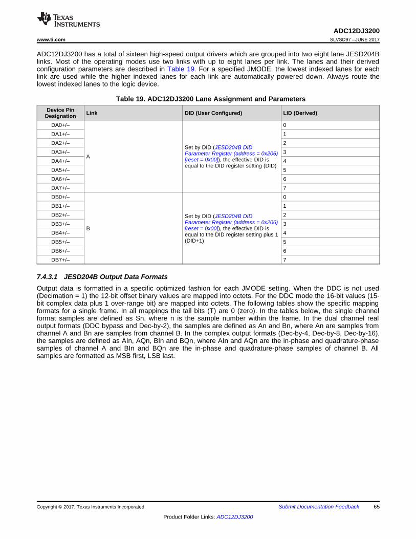
65
ADC12DJ3200www.ti.com SLVSD97 –JUNE 2017
Product Folder Links: ADC12DJ3200
Submit Documentation FeedbackCopyright © 2017, Texas Instruments Incorporated
ADC12DJ3200 has a total of sixteen high-speed output drivers which are grouped into two eight lane JESD204Blinks. Most of the operating modes use two links with up to eight lanes per link. The lanes and their derivedconfiguration parameters are described in Table 19. For a specified JMODE, the lowest indexed lanes for eachlink are used while the higher indexed lanes for each link are automatically powered down. Always route thelowest indexed lanes to the logic device.
Table 19. ADC12DJ3200 Lane Assignment and ParametersDevice Pin
Designation Link DID (User Configured) LID (Derived)
DA0+/–
A
Set by DID (JESD204B DIDParameter Register (address = 0x206)[reset = 0x00]), the effective DID isequal to the DID register setting (DID)
0DA1+/– 1DA2+/– 2DA3+/– 3DA4+/– 4DA5+/– 5DA6+/– 6DA7+/– 7DB0+/–
B
Set by DID (JESD204B DIDParameter Register (address = 0x206)[reset = 0x00]), the effective DID isequal to the DID register setting plus 1(DID+1)
0DB1+/– 1DB2+/– 2DB3+/– 3DB4+/– 4DB5+/– 5DB6+/– 6DB7+/– 7
7.4.3.1 JESD204B Output Data FormatsOutput data is formatted in a specific optimized fashion for each JMODE setting. When the DDC is not used(Decimation = 1) the 12-bit offset binary values are mapped into octets. For the DDC mode the 16-bit values (15-bit complex data plus 1 over-range bit) are mapped into octets. The following tables show the specific mappingformats for a single frame. In all mappings the tail bits (T) are 0 (zero). In the tables below, the single channelformat samples are defined as Sn, where n is the sample number within the frame. In the dual channel realoutput formats (DDC bypass and Dec-by-2), the samples are defined as An and Bn, where An are samples fromchannel A and Bn are samples from channel B. In the complex output formats (Dec-by-4, Dec-by-8, Dec-by-16),the samples are defined as AIn, AQn, BIn and BQn, where AIn and AQn are the in-phase and quadrature-phasesamples of channel A and BIn and BQn are the in-phase and quadrature-phase samples of channel B. Allsamples are formatted as MSB first, LSB last.
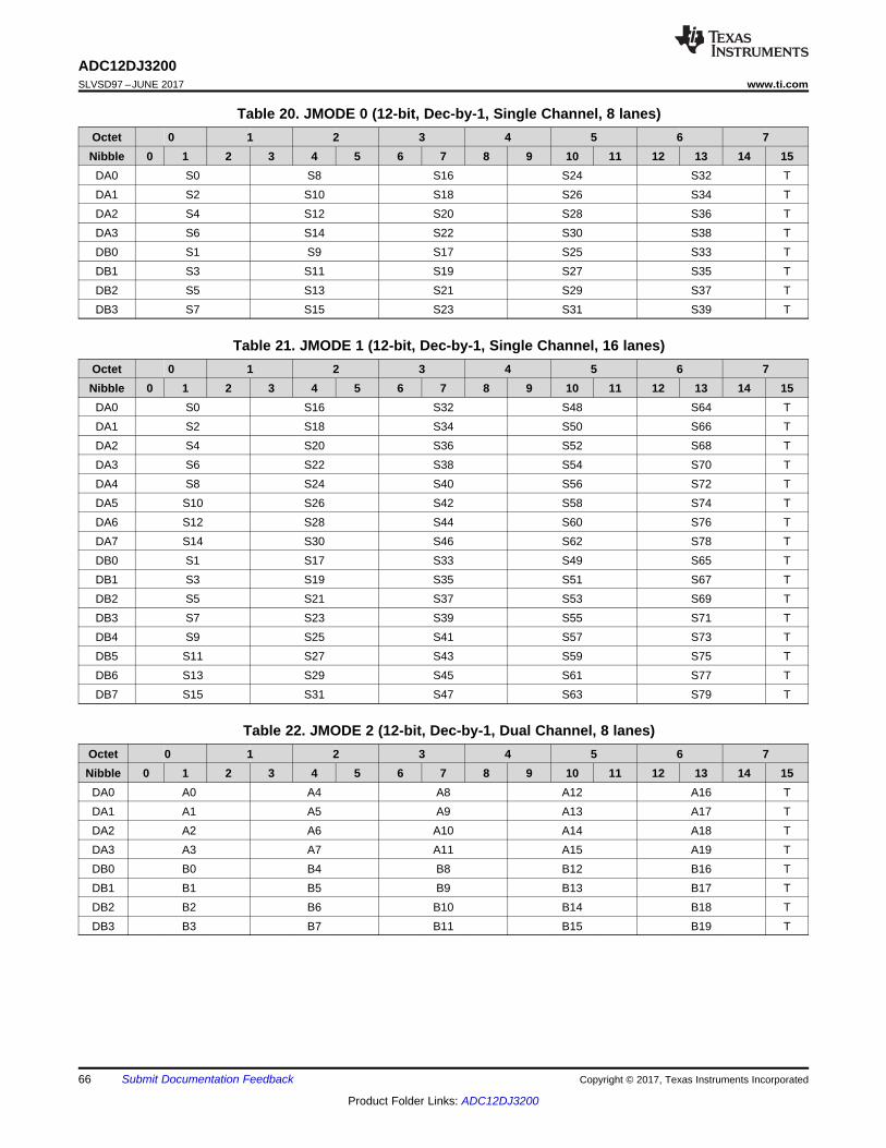
66
ADC12DJ3200SLVSD97 –JUNE 2017 www.ti.com
Product Folder Links: ADC12DJ3200
Submit Documentation Feedback Copyright © 2017, Texas Instruments Incorporated
Table 20. JMODE 0 (12-bit, Dec-by-1, Single Channel, 8 lanes)Octet 0 1 2 3 4 5 6 7Nibble 0 1 2 3 4 5 6 7 8 9 10 11 12 13 14 15DA0 S0 S8 S16 S24 S32 TDA1 S2 S10 S18 S26 S34 TDA2 S4 S12 S20 S28 S36 TDA3 S6 S14 S22 S30 S38 TDB0 S1 S9 S17 S25 S33 TDB1 S3 S11 S19 S27 S35 TDB2 S5 S13 S21 S29 S37 TDB3 S7 S15 S23 S31 S39 T
Table 21. JMODE 1 (12-bit, Dec-by-1, Single Channel, 16 lanes)Octet 0 1 2 3 4 5 6 7Nibble 0 1 2 3 4 5 6 7 8 9 10 11 12 13 14 15DA0 S0 S16 S32 S48 S64 TDA1 S2 S18 S34 S50 S66 TDA2 S4 S20 S36 S52 S68 TDA3 S6 S22 S38 S54 S70 TDA4 S8 S24 S40 S56 S72 TDA5 S10 S26 S42 S58 S74 TDA6 S12 S28 S44 S60 S76 TDA7 S14 S30 S46 S62 S78 TDB0 S1 S17 S33 S49 S65 TDB1 S3 S19 S35 S51 S67 TDB2 S5 S21 S37 S53 S69 TDB3 S7 S23 S39 S55 S71 TDB4 S9 S25 S41 S57 S73 TDB5 S11 S27 S43 S59 S75 TDB6 S13 S29 S45 S61 S77 TDB7 S15 S31 S47 S63 S79 T
Table 22. JMODE 2 (12-bit, Dec-by-1, Dual Channel, 8 lanes)Octet 0 1 2 3 4 5 6 7Nibble 0 1 2 3 4 5 6 7 8 9 10 11 12 13 14 15
DA0 A0 A4 A8 A12 A16 TDA1 A1 A5 A9 A13 A17 TDA2 A2 A6 A10 A14 A18 TDA3 A3 A7 A11 A15 A19 TDB0 B0 B4 B8 B12 B16 TDB1 B1 B5 B9 B13 B17 TDB2 B2 B6 B10 B14 B18 TDB3 B3 B7 B11 B15 B19 T

67
ADC12DJ3200www.ti.com SLVSD97 –JUNE 2017
Product Folder Links: ADC12DJ3200
Submit Documentation FeedbackCopyright © 2017, Texas Instruments Incorporated
Table 23. JMODE 3 (12-bit, Dec-by-1, Dual Channel, 16 lanes)Octet 0 1 2 3 4 5 6 7Nibble 0 1 2 3 4 5 6 7 8 9 10 11 12 13 14 15
DA0 A0 A8 A16 A24 A32 TDA1 A1 A9 A17 A25 A33 TDA2 A2 A10 A18 A26 A34 TDA3 A3 A11 A19 A27 A35 TDA4 A4 A12 A20 A28 A36 TDA5 A5 A13 A21 A29 A37 TDA6 A6 A14 A22 A30 A38 TDA7 A7 A15 A23 A31 A39 TDB0 B0 B8 B16 B24 B32 TDB1 B1 B9 B17 B25 B33 TDB2 B2 B10 B18 B26 B34 TDB3 B3 B11 B19 B27 B35 TDB4 B4 B12 B20 B28 B36 TDB5 B5 B13 B21 B29 B37 TDB6 B6 B14 B22 B30 B38 TDB7 B7 B15 B23 B31 B39 T
Table 24. JMODE 4 (8-bit, Dec-by-1, Single Channel, 4 lanes)Octet 0Nibble 0 1
DA0 S0DA1 S2DB0 S1DB1 S3
Table 25. JMODE 5 (8-bit, Dec-by-1, Single Channel, 8 lanes)Octet 0Nibble 0 1
DA0 S0DA1 S2DA2 S4DA3 S6DB0 S1DB1 S3DB2 S5DB3 S7
Table 26. JMODE 6 (8-bit, Dec-by-1, Dual Channel, 4 lanes)Octet 0Nibble 0 1
DA0 A0DA1 A1DB0 B0DB1 B1
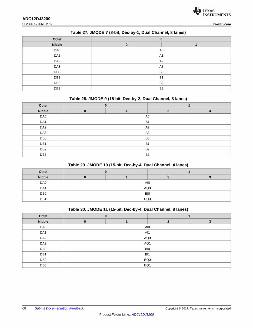
68
ADC12DJ3200SLVSD97 –JUNE 2017 www.ti.com
Product Folder Links: ADC12DJ3200
Submit Documentation Feedback Copyright © 2017, Texas Instruments Incorporated
Table 27. JMODE 7 (8-bit, Dec-by-1, Dual Channel, 8 lanes)Octet 0Nibble 0 1
DA0 A0DA1 A1DA2 A2DA3 A3DB0 B0DB1 B1DB2 B2DB3 B3
Table 28. JMODE 9 (15-bit, Dec-by-2, Dual Channel, 8 lanes)Octet 0 1Nibble 0 1 2 3
DA0 A0DA1 A1DA2 A2DA3 A3DB0 B0DB1 B1DB2 B2DB3 B3
Table 29. JMODE 10 (15-bit, Dec-by-4, Dual Channel, 4 lanes)Octet 0 1Nibble 0 1 2 3
DA0 AI0DA1 AQ0DB0 BI0DB1 BQ0
Table 30. JMODE 11 (15-bit, Dec-by-4, Dual Channel, 8 lanes)Octet 0 1Nibble 0 1 2 3
DA0 AI0DA1 AI1DA2 AQ0DA3 AQ1DB0 BI0DB1 BI1DB2 BQ0DB3 BQ1

69
ADC12DJ3200www.ti.com SLVSD97 –JUNE 2017
Product Folder Links: ADC12DJ3200
Submit Documentation FeedbackCopyright © 2017, Texas Instruments Incorporated
Table 31. JMODE 12 (12-bit, Dec-by-4, Dual Channel, 16 lanes)Octet 0 1 2 3 4 5 6 7Nibble 0 1 2 3 4 5 6 7 8 9 10 11 12 13 14 15DA0 AI0 AI4 AI8 AI12 AI16 TDA1 AQ0 AQ4 AQ8 AQ12 AQ16 TDA2 AI1 AI5 AI9 AI13 AI17 TDA3 AQ1 AQ5 AQ9 AQ13 AQ17 TDA4 AI2 AI6 AI10 AI14 AI18 TDA5 AQ2 AQ6 AQ10 AQ14 AQ218 TDA6 AI3 AI7 AI11 AI15 AI19 TDA7 AQ3 AQ7 AQ11 AQ15 AQ19 TDB0 BI0 BI4 BI8 BI12 BI16 TDB1 BQ0 BQ4 BQ8 BQ12 BQ16 TDB2 BI1 BI5 BI9 BI13 BI17 TDB3 BQ1 BQ5 BQ9 BQ13 BQ17 TDB4 BI2 BI6 BI10 BI14 BI18 TDB5 BQ2 BQ6 BQ10 BQ14 BQ218 TDB6 BI3 BI7 BI11 BI15 BI19 TDB7 BQ3 BQ7 BQ11 BQ15 BQ19 T
Table 32. JMODE 13 (15-bit, Dec-by-8, Dual Channel, 2 lanes)Octet 0 1 2 3
Nibble 0 1 2 3 4 5 6 7
DA0 AI0 AQ0
DB0 BI0 BQ0
Table 33. JMODE 14 (15-bit, Dec-by-8, Dual Channel, 4 lanes)Octet 0 1
Nibble 0 1 2 3
DA0 AI0
DA1 AQ0
DB0 BI0
DB1 BQ0
Table 34. JMODE 15 (15-bit, Dec-by-16, Dual Channel, 1 lane)Octet 0 1 2 3 4 5 6 7Nibble 0 1 2 3 4 5 6 7 8 9 10 11 12 13 14 15
DA0 AI0 AQ0 BI0 BQ0
Table 35. JMODE 16 (15-bit, Dec-by-16, Dual Channel, 2 lanes)Octet 0 1 2 3Nibble 0 1 2 3 4 5 6 7
DA0 AI0 AQ0DB0 BI0 BQ0

70
ADC12DJ3200SLVSD97 –JUNE 2017 www.ti.com
Product Folder Links: ADC12DJ3200
Submit Documentation Feedback Copyright © 2017, Texas Instruments Incorporated
Table 36. JMODE 17 (8-bit, Dec-by-1, Single Channel, 16 lanes)Octet 0Nibble 0 1
DA0 S0DA1 S2DA2 S4DA3 S6DA4 S8DA5 S10DA6 S12DA7 S14DB0 S1DB1 S3DB2 S5DB3 S7DB4 S9DB5 S11DB6 S13DB7 S15
Table 37. JMODE 18 (8-bit, Dec-by-1, Dual Channel, 16 lanes)Octet 0Nibble 0 1
DA0 A0DA1 A1DA2 A2DA3 A3DA4 A4DA5 A5DA6 A6DA7 A7DB0 B0DB1 B1DB2 B2DB3 B3DB4 B4DB5 B5DB6 B6DB7 B7
7.4.3.2 Dual DDC and Redundant Data ModeWhen operating in dual channel mode the data from one channel can be routed to both digital down-converterblocks by using DIG_BIND_A or DIG_BIND_B (Digital Channel Binding Register (address = 0x216) [reset =0x02]). This enables down-conversion of two separate captured bands from a single ADC channel. The secondADC can be powered down in this mode by setting PD_ACH or PD_BCH (Device Configuration Register(address = 0x002) [reset = 0x00]).

MU
X
DIG_BIND_A = 0
ADC
Channel A
ADC
Channel B
JESD204B
LINK A
(DA0-DA7)DDC A
MU
X
JMODE
DDC Bypass
MU
X
JESD204B
LINK B
(DB0-DB7)DDC B
MU
X
JMODE
DDC Bypass
DIG_BIND_B = 0
Copyright © 2016, Texas Instruments Incorporated
71
ADC12DJ3200www.ti.com SLVSD97 –JUNE 2017
Product Folder Links: ADC12DJ3200
Submit Documentation FeedbackCopyright © 2017, Texas Instruments Incorporated
Additionally, DIG_BIND_A or DIG_BIND_B can be used to provide redundant data to separate digital processorsby routing data from one ADC channel to both JESD204B links. Redundant data mode is available for all JMODEmodes except for the single channel modes. Both dual DDC mode and redundant data mode are demonstratedin Figure 84 where the data for ADC channel A is routed to both DDCs and then transmitted to a singleprocessor or two processors (for redundancy).
Figure 84. Dual DDC Mode or Redundant Data Mode for Channel A
7.4.4 Power Down Modes
NOTEPower down of the high speed data outputs (DA0+/– ... DA7+/–, DB0+/– ... DB7+/–) forextended times may reduce performance of the output serializers, especially at high datarates. Please see note beneath Recommended Operating Conditions for more information.
The PD input pin allows the ADC12DJ3200 devices to be entirely powered down. Power down can also becontrolled by MODE (Device Configuration Register (address = 0x002) [reset = 0x00]). The serial data outputdrivers are disabled when PD is high. When the device returns to normal operation, the JESD204 link must bere-established, and the ADC pipeline contain meaningless information so the system must wait a sufficient timefor the data to be flushed. If power down for power savings is desired the system should power down the supplyvoltages regulators for VA19, VA11 and VD11 rather than make use of the PD input or MODE settings.
7.4.5 Test ModesA number of device test modes are available. These modes insert known patterns of information into the devicedata path for assistance with system debug, development, or characterization.
7.4.5.1 Serializer Test-Mode DetailsTest modes are enabled by setting JTEST (JESD204B Test Pattern Control Register (address = 0x205) [reset =0x00]) to the desired test mode. Each test mode is described in detail in the following sections. Regardless of thetest mode, the serializer outputs are powered up based on JMODE. The test modes should only be enabledwhile the JESD204B link is disabled.
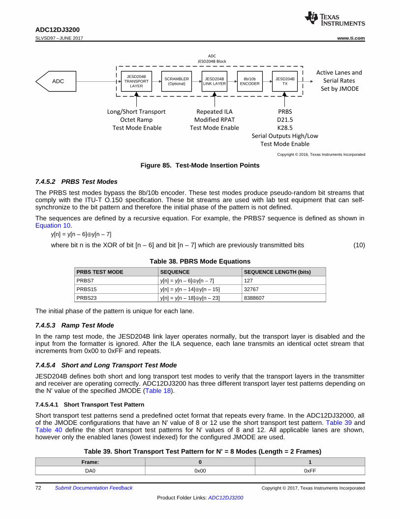
ADCJESD204B
TRANSPORT LAYER
SCRAMBLER(Optional)
JESD204BLINK LAYER
JESD204BTX
8b/10bENCODER
ADC
JESD204B Block
Long/Short Transport
Octet Ramp
Test Mode Enable
Repeated ILA
Modified RPAT
Test Mode Enable
PRBS
D21.5
K28.5
Serial Outputs High/Low
Test Mode Enable
Active Lanes and
Serial Rates
Set by JMODE
Copyright © 2016, Texas Instruments Incorporated
72
ADC12DJ3200SLVSD97 –JUNE 2017 www.ti.com
Product Folder Links: ADC12DJ3200
Submit Documentation Feedback Copyright © 2017, Texas Instruments Incorporated
Figure 85. Test-Mode Insertion Points
7.4.5.2 PRBS Test ModesThe PRBS test modes bypass the 8b/10b encoder. These test modes produce pseudo-random bit streams thatcomply with the ITU-T O.150 specification. These bit streams are used with lab test equipment that can self-synchronize to the bit pattern and therefore the initial phase of the pattern is not defined.
The sequences are defined by a recursive equation. For example, the PRBS7 sequence is defined as shown inEquation 10.
y[n] = y[n – 6]⊕y[n – 7]
where bit n is the XOR of bit [n – 6] and bit [n – 7] which are previously transmitted bits (10)
Table 38. PBRS Mode EquationsPRBS TEST MODE SEQUENCE SEQUENCE LENGTH (bits)PRBS7 y[n] = y[n – 6]⊕y[n – 7] 127PRBS15 y[n] = y[n – 14]⊕y[n – 15] 32767PRBS23 y[n] = y[n – 18]⊕y[n – 23] 8388607
The initial phase of the pattern is unique for each lane.
7.4.5.3 Ramp Test ModeIn the ramp test mode, the JESD204B link layer operates normally, but the transport layer is disabled and theinput from the formatter is ignored. After the ILA sequence, each lane transmits an identical octet stream thatincrements from 0x00 to 0xFF and repeats.
7.4.5.4 Short and Long Transport Test ModeJESD204B defines both short and long transport test modes to verify that the transport layers in the transmitterand receiver are operating correctly. ADC12DJ3200 has three different transport layer test patterns depending onthe N' value of the specified JMODE (Table 18).
7.4.5.4.1 Short Transport Test Pattern
Short transport test patterns send a predefined octet format that repeats every frame. In the ADC12DJ32000, allof the JMODE configurations that have an N' value of 8 or 12 use the short transport test pattern. Table 39 andTable 40 define the short transport test patterns for N' values of 8 and 12. All applicable lanes are shown,however only the enabled lanes (lowest indexed) for the configured JMODE are used.
Table 39. Short Transport Test Pattern for N' = 8 Modes (Length = 2 Frames)Frame: 0 1
DA0 0x00 0xFF
73
ADC12DJ3200www.ti.com SLVSD97 –JUNE 2017
Product Folder Links: ADC12DJ3200
Submit Documentation FeedbackCopyright © 2017, Texas Instruments Incorporated
Table 39. Short Transport Test Pattern for N' = 8 Modes (Length = 2 Frames) (continued)Frame: 0 1
DA1 0x01 0xFEDA2 0x02 0xFDDA3 0x03 0xFCDB0 0x00 0xFFDB1 0x01 0xFEDB2 0x02 0xFDDB3 0x03 0xFC
Table 40. Short Transport Test Pattern for N' = 12 Modes (Length = 1 Frame)Octet 0 1 2 3 4 5 6 7Nibble 0 1 2 3 4 5 6 7 8 9 10 11 12 13 14 15
DA0 0xF01 0xF02 0xF03 0xF04 0xF05 TDA1 0xE11 0xE12 0xE13 0xE14 0xE15 TDA2 0xD21 0xD22 0xD23 0xD24 0xD25 TDA3 0xC31 0xC32 0xC33 0xC34 0xC35 TDA4 0xB41 0xB42 0xB43 0xB44 0xB45 TDA5 0xA51 0xA52 0xA53 0xA54 0xA55 TDA6 0x961 0x962 0x963 0x964 0x965 TDA7 0x871 0x872 0x873 0x874 0x875 TDB0 0xF01 0xF02 0xF03 0xF04 0xF05 TDB1 0xE11 0xE12 0xE13 0xE14 0xE15 TDB2 0xD21 0xD22 0xD23 0xD24 0xD25 TDB3 0xC31 0xC32 0xC33 0xC34 0xC35 TDB4 0xB41 0xB42 0xB43 0xB44 0xB45 TDB5 0xA51 0xA52 0xA53 0xA54 0xA55 TDB6 0x961 0x962 0x963 0x964 0x965 TDB7 0x871 0x872 0x873 0x874 0x875 T
7.4.5.4.2 Long Transport Test Pattern
The long-transport test mode is used in all of the JMODE modes where N' equals 16. Patterns are generated inaccordance with the JESD204B standard and are different for each output format as defined in Table 18. Therules for the pattern are defined below. The length of the test pattern is given by Equation 11. The long transporttest pattern is the same for link A and link B, where DAx lanes belong to link A and DBx lanes belong to link B.Long Test Pattern Length (Frames) = K * ceil((M*S+2) / K) (11)
• Sample Data:– Frame 0: Each sample contains N bits, with all samples set to the converter id (CID) plus 1 (CID + 1). CID
is defined based on the converter number within the link; note that two links are used in all modes exceptJMODE 15. Within a link, the converters are numbered by channel (A or B) and in-phase (I) andquadrature-phase (Q) and reset between links. For instance, in JMODE 10, two links are used so channelA and B data is separated into separate links and the in-phase component for each channel has CID = 0and the quadrature-phase component has CID = 1. In JMODE 15, one link is used, so channel A and Bare within the same link and AI has CID = 0, AQ has CID = 1, BI has CID = 2, and BQ has CID = 3.
– Frame 1: Each sample contains N bits, with each sample (for each converter) set as its individual sampleID (SID) within the frame plus 1 (SID + 1)
– Frame 2 +: Each sample contains N bits, with the data set to 2N–1 for all samples, for example if N is 15,then 2N–1 = 16384
• Control Bits (if CS > 0):– Frame 0 to M*S–1: The control bit belonging to sample mod(i,S) of converter floor(i,S) set to "1" and all
others set to "0", where i is the frame index (i=0 is the first frame of the pattern). Essentially, the control bit

74
ADC12DJ3200SLVSD97 –JUNE 2017 www.ti.com
Product Folder Links: ADC12DJ3200
Submit Documentation Feedback Copyright © 2017, Texas Instruments Incorporated
"walks" from the lowest indexed sample to the highest indexed sample and from the lowest indexedconverter to highest indexed converter, changing position every frame.
– Frame M*S +: All control bits set to 0
Table 41. Example Long Transport Test Pattern - JMODE = 10, K = 10TIME → Pattern
Repeats →
OCTETNUM.
0 1 2 3 4 5 6 7 8 9 10 11 12 13 14 15 16 17 18 19 20 21
DA0 0x0003 0x0002 0x8000 0x8000 0x8000 0x8000 0x8000 0x8000 0x8000 0x8000 0x0003
DA1 0x0004 0x0003 0x8000 0x8000 0x8000 0x8000 0x8000 0x8000 0x8000 0x8000 0x0004
DB0 0x0003 0x0002 0x8000 0x8000 0x8000 0x8000 0x8000 0x8000 0x8000 0x8000 0x0003
DB1 0x0004 0x0003 0x8000 0x8000 0x8000 0x8000 0x8000 0x8000 0x8000 0x8000 0x0004
Framen
Framen + 1
Framen + 2
Framen + 3
Framen + 4
Framen + 5
Framen + 6
Framen + 7
Framen + 8
Framen + 9
Framen + 10
The pattern starts at the end of the initial lane alignment sequence (ILAS) and repeats indefinitely as long as thelink remains running. For more details see JESD204B, section 5.1.6.3.
7.4.5.5 D21.5 Test ModeIn this test mode, the controller transmits a continuous stream of D21.5 characters (alternating 0s and 1s).
7.4.5.6 K28.5 Test ModeIn this test mode, the controller transmits a continuous stream of K28.5 characters.
7.4.5.7 Repeated ILA Test ModeIn this test mode, the JESD204B link layer operates normally, except that the ILA sequence (ILAS) repeatsindefinitely instead of starting the data phase. Whenever the receiver issues a synchronization request, thetransmitter will initiate code group synchronization. Upon completion of code group synchronization, thetransmitter will repeatedly transmit the ILA sequence.
7.4.5.8 Modified RPAT Test ModeA 12-octet repeating pattern is defined in INCITS TR-35-2004. The purpose of this pattern is to generate whitespectral content for JESD204B compliance and jitter testing. Table 42 lists the pattern before and after 8b10bencoding.
Table 42. Modified RPAT Pattern Values
OCTET NUMBER Dx.y NOTATION 8-BIT INPUT TO 8b10b ENCODER 20b OUTPUT OF 8b10b ENCODER(2 CHARACTERS)
0 D30.5 0xBE0x86BA6
1 D23.6 0xD7
2 D3.1 0x230xC6475
3 D7.2 0x47
4 D11.3 0x6B0xD0E8D
5 D15.4 0x8F
6 D19.5 0xB30xCA8B4
7 D20.0 0x14
8 D30.2 0x5E0x7949E
9 D27.7 0xFB
10 D21.1 0x350xAA665
11 D25.2 0x59
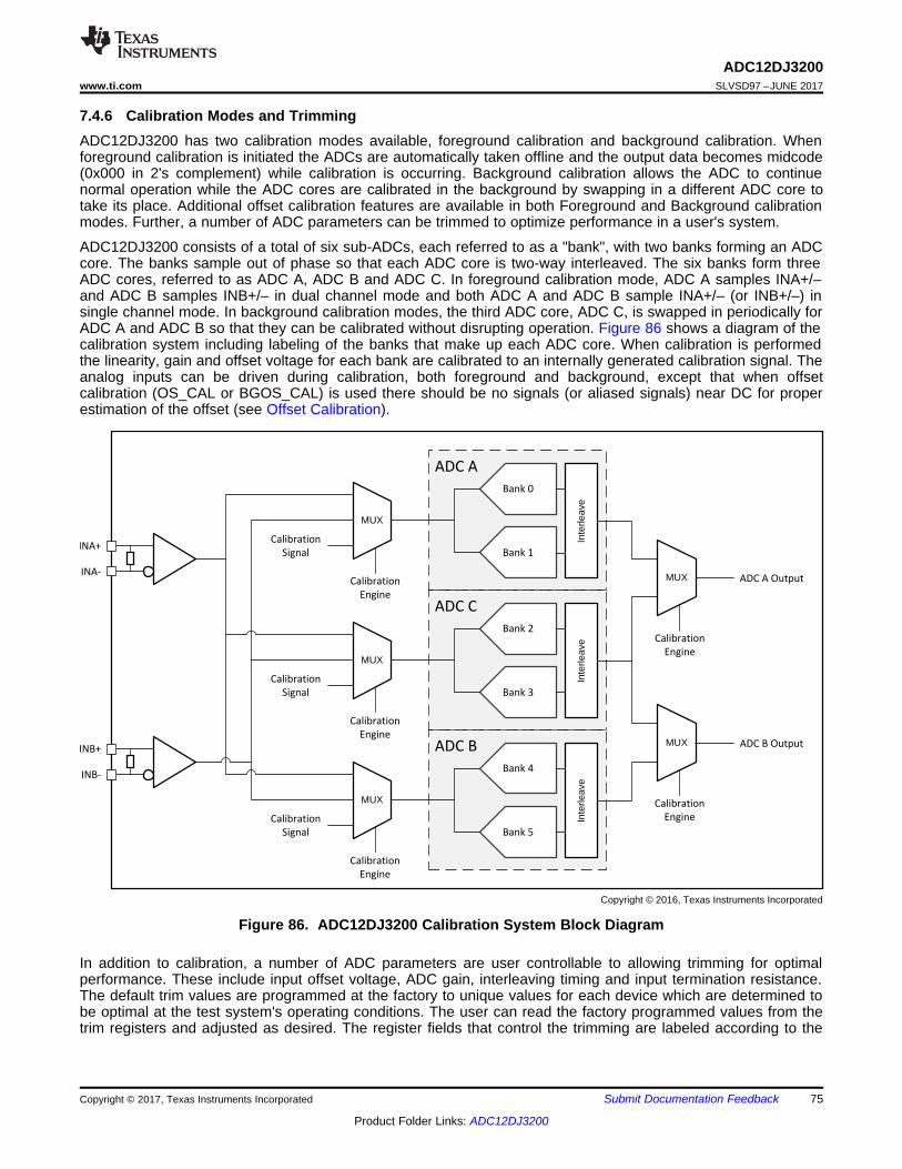
ADC A
INA+
INA-
INB+
INB-
Calibration
Signal
Calibration
Signal
Calibration
Signal
Bank 1
Bank 0
ADC C
Bank 3
Bank 2
ADC B
Bank 5
Bank 4
Calibration
Engine
MUX
MUX
MUX
MUX
MUX
ADC A Output
ADC B Output
Calibration
Engine
Calibration
Engine
Calibration
Engine
Calibration
Engine
Inte
rleav
eIn
terle
ave
Inte
rleav
e
Copyright © 2016, Texas Instruments Incorporated
75
ADC12DJ3200www.ti.com SLVSD97 –JUNE 2017
Product Folder Links: ADC12DJ3200
Submit Documentation FeedbackCopyright © 2017, Texas Instruments Incorporated
7.4.6 Calibration Modes and TrimmingADC12DJ3200 has two calibration modes available, foreground calibration and background calibration. Whenforeground calibration is initiated the ADCs are automatically taken offline and the output data becomes midcode(0x000 in 2's complement) while calibration is occurring. Background calibration allows the ADC to continuenormal operation while the ADC cores are calibrated in the background by swapping in a different ADC core totake its place. Additional offset calibration features are available in both Foreground and Background calibrationmodes. Further, a number of ADC parameters can be trimmed to optimize performance in a user's system.
ADC12DJ3200 consists of a total of six sub-ADCs, each referred to as a "bank", with two banks forming an ADCcore. The banks sample out of phase so that each ADC core is two-way interleaved. The six banks form threeADC cores, referred to as ADC A, ADC B and ADC C. In foreground calibration mode, ADC A samples INA+/–and ADC B samples INB+/– in dual channel mode and both ADC A and ADC B sample INA+/– (or INB+/–) insingle channel mode. In background calibration modes, the third ADC core, ADC C, is swapped in periodically forADC A and ADC B so that they can be calibrated without disrupting operation. Figure 86 shows a diagram of thecalibration system including labeling of the banks that make up each ADC core. When calibration is performedthe linearity, gain and offset voltage for each bank are calibrated to an internally generated calibration signal. Theanalog inputs can be driven during calibration, both foreground and background, except that when offsetcalibration (OS_CAL or BGOS_CAL) is used there should be no signals (or aliased signals) near DC for properestimation of the offset (see Offset Calibration).
Figure 86. ADC12DJ3200 Calibration System Block Diagram
In addition to calibration, a number of ADC parameters are user controllable to allowing trimming for optimalperformance. These include input offset voltage, ADC gain, interleaving timing and input termination resistance.The default trim values are programmed at the factory to unique values for each device which are determined tobe optimal at the test system's operating conditions. The user can read the factory programmed values from thetrim registers and adjusted as desired. The register fields that control the trimming are labeled according to the

76
ADC12DJ3200SLVSD97 –JUNE 2017 www.ti.com
Product Folder Links: ADC12DJ3200
Submit Documentation Feedback Copyright © 2017, Texas Instruments Incorporated
input that is being sampled (INA+/– or INB+/–), the bank that is being trimmed or the ADC core that is beingtrimmed. It is not expected that the user must change the trim values as operating conditions change, howeveroptimal performance may be obtained by doing so. Any custom trimming must be done on a per device basisdue to process variations, meaning that there is no global optimal setting for all parts. See Trimming forinformation about the available trim parameters and associated registers.
7.4.6.1 Foreground Calibration ModeForeground calibration requires the ADC to stop converting the analog input signals during the procedure.Foreground calibration always runs on power up and the user must wait a sufficient time before programming thedevice to guarantee that the calibration is finished. Foreground calibration can be initiated by triggering thecalibration engine. The trigger source can be either the CAL_TRIG pin or CAL_SOFT_TRIG (CalibrationSoftware Trigger Register (address = 0x06C) [reset = 0x01]) and is chosen by setting CAL_TRIG_EN(Calibration Pin Configuration Register (address = 0x06B) [reset = 0x00]).
7.4.6.2 Background Calibration ModeBackground calibration mode allows the ADC to continuously operate, with no interruption of data. This isaccomplished by activating an extra ADC core which is calibrated and then takes over operation for one of theother previously active ADC cores. Once that ADC core is taken off-line it is then calibrated and can in turn takeover to allow the next ADC to be calibrated. This process operates continuously, ensuring the ADC cores arealways providing the optimum performance regardless of system operating condition changes. Due to theadditional active ADC core, Background calibration mode has increased power consumption in comparison toForeground calibration mode. The low-power background calibration (LPBG) mode discussed next providesreduced average power consumption in comparison with the standard background calibration mode. Backgroundcalibration can be enabled by setting CAL_BG (Calibration Configuration 0 Register (address = 0x062) [reset =0x01]). CAL_TRIG_EN should be set to 0 and CAL_SOFT_TRIG should be set to 1.
Great care has been taken to minimize effects on converted data as the core switching process occurs, however,small brief glitches may still be seen on the converter data as the cores are swapped. Please refer to the TypicalCharacteristic section of the datasheet for examples of the possible glitches in sine-wave and DC signals.
7.4.6.3 Low-Power Background Calibration (LPBG) ModeLow-power background calibration (LPBG) mode reduces the power-overhead of enabling additional ADC cores.Off-line cores are powered down until ready to be calibrated and put on-line. Set LP_EN=1 to enable the low-power background calibration feature. LP_SLEEP_DLY is used to adjust the amount of time an ADC sleepsbefore waking up for calibration (if LP_EN=1 and LP_TRIG=0). LP_WAKE_DLY sets how long the core isallowed to stabilize before calibration and being put on-line. LP_TRIG is used to select between an automaticswitching process or one that is controlled by the user via CAL_SOFT_TRIG or CAL_TRIG. In this mode there isan increase in power consumption during the ADC core calibration. The power consumption will roughly alternatebetween the power consumption in foreground calibration when the spare ADC core is sleeping to the powerconsumption in background calibration when the spare ADC is being calibrated. The power supply networkshould be designed to be able to handle the transient power requirements for this mode.
7.4.7 Offset CalibrationForeground calibration and background calibration modes inherently calibrate the offsets of the ADC cores,however the input buffers sits outside of the calibration loop and therefore their offsets are not calibrated by thestandard calibration process. In both dual channel mode and single channel mode uncalibrated input bufferoffsets result in a shift in the mid-code output (DC offset) with no input. Further, in single channel modeuncalibrated input buffer offsets can result in a fixed spur at FS/2. A separate calibration is provided to correct theinput buffer offsets.
77
ADC12DJ3200www.ti.com SLVSD97 –JUNE 2017
Product Folder Links: ADC12DJ3200
Submit Documentation FeedbackCopyright © 2017, Texas Instruments Incorporated
There must be no signals at or near DC or aliased signals that fall at or near DC in order to properly calibrationthe offsets, requiring the system to guarantee this condition during normal operation or have the ability to mutethe input signal during calibration. Foreground offset calibration is enabled via CAL_OS and only performs thecalibration once as part of the foreground calibration procedure. Background offset calibration is enabled viaCAL_BGOS and will continue to correct the offset as part of the background calibration routine to account foroperating condition changes. When CAL_BGOS is set the system must guarantee that there are no DC or nearDC signals or aliased signals that fall at or near DC during normal operation. Offset calibration can be performedas a foreground operation when using background calibration by setting CAL_OS to 1 before setting CAL_EN,but it will not correct for variations as operating conditions change.
The offset calibration correction uses the input offset voltage trim registers (see Table 43) to correct the offsetand therefore must not be written by the user when offset calibration is used. The user can read the calibratedvalues by reading the OADJ_x_VINy registers, where x is the ADC core and y is the input (INA+/– or INB+/–),after calibration is completed. The values should only be read when FG_DONE is read as 1 when usingforeground offset calibration (CAL_OS = 1) and should not be read when using background offset calibration(CAL_BGOS = 1).
7.4.8 TrimmingThe parameters that can be trimmed and the associated registers are summarized in Table 43.
Table 43. Trim Register DescriptionsTrim Parameter Trim Register Notes
Bandgap reference BG_TRIM Measure on BG output pin.
Input termination resistance RTRIM_xWhere x = A for INA+/– or B for INB+/–)
Device must be powered on with a clockapplied.
Input offset voltageOADJ_x_VINy
Where x = ADC core (A, B or C)and y = A for INA+/– or B for INB+/–)
A different trim value is allowed for eachADC core (A, B or C) to allow moreconsistent offset performance in backgroundcalibration mode.
INA+/– and INB+/– gain GAIN_TRIM_xWhere x = A for INA+/– or B for INB+/–)
FS_RANGE_A and FS_RANGE_B should beset to default values before trimming theinput. FS_RANGE_A and FS_RANGE_Bshould be used to adjust the full scale inputvoltage.
INA+/– and INB+/– full scale input voltage FS_RANGE_xWhere x = A for INA+/– or B for INB+/–)
Full scale input voltage adjustment for eachinput. The default value is effected byGAIN_TRIM_x (x = A or B). GAIN_TRIM_xshould be trimmed with FS_RANGE_x set tothe default value. FS_RANGE_x can then beused to trim the full scale input voltage.
Intra-ADC core timing (bank timing)Bx_TIME_y
Where x = bank number (0–5)and y = 0° or –90° clock phase
Trims the timing between the two banks ofan ADC core (ADC A, B or C) for two clockphases, either 0° or –90°. The –90° clockphase is used in single channel mode only.
Inter-ADC core timing (dual channel mode) TADJ_A, TADJ_B, TADJ_CA, TADJ_CB
The suffix letter (A, B, CA or CB) indicatesthe ADC core that is being trimmed. CAindicates that this is the timing trim inbackground calibration mode for ADC Cwhen it is standing in for ADC A, whereasCB is timing trim for ADC C when it isstanding in for ADC B.
78
ADC12DJ3200SLVSD97 –JUNE 2017 www.ti.com
Product Folder Links: ADC12DJ3200
Submit Documentation Feedback Copyright © 2017, Texas Instruments Incorporated
Table 43. Trim Register Descriptions (continued)Trim Parameter Trim Register Notes
Inter-ADC core timing (single channel mode)TADJ_A_FG90, TADJ_B_FG0,TADJ_A_BG90, TADJ_C_BG0,TADJ_C_BG90, TADJ_B_BG0
The middle letter (A, B or C) indicates theADC core that is being trimmed. FG indicatesthat it is a trim for foreground calibrationwhile BG indicates background calibration.The suffix of 0 or 90 indicates the clockphase applied to the ADC core. 0 indicates a0° clock and is sampling in-phase with theclock input. 90 indicates a 90° clock andtherefore is sampling out-of-phase with theclock input. These timings must be trimmedfor optimal performance if the user prefers touse INB+/– in single channel mode. They aretrimmed for INA+/– at the factory.
7.4.9 Offset FilteringThe ADC12DJ3200 has an additional feature which can be enabled to reduce offset related interleaving spurs atFs/2 and Fs/4 (single input mode only). Offset filtering is enabled via CAL_OSFILT. The OSFILT_BW andOSFILT_SOAK parameters can be adjusted to tradeoff offset spur reduction with potential impact on informationin the mission mode signal being processed. These two parameters should be set to the same value under mostsituations. The DC_RESTORE setting is used to either retain or filter out all DC related content in the signal.
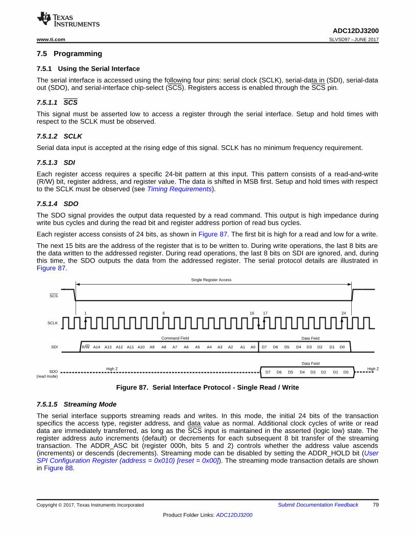
SCLK
1 24
Single Register Access
SCS
SDI
Command Field Data Field
SDO (read mode)
Data FieldHigh Z High Z
17168
A14 A13 A12 A11 A10 A9 A8 A7 A6 A5 A4 A3 A2 A1 A0 D7 D6 D5 D4 D3 D2 D1 D0
D7 D6 D5 D4 D3 D2 D1 D0
R/W
79
ADC12DJ3200www.ti.com SLVSD97 –JUNE 2017
Product Folder Links: ADC12DJ3200
Submit Documentation FeedbackCopyright © 2017, Texas Instruments Incorporated
7.5 Programming
7.5.1 Using the Serial InterfaceThe serial interface is accessed using the following four pins: serial clock (SCLK), serial-data in (SDI), serial-dataout (SDO), and serial-interface chip-select (SCS). Registers access is enabled through the SCS pin.
7.5.1.1 SCSThis signal must be asserted low to access a register through the serial interface. Setup and hold times withrespect to the SCLK must be observed.
7.5.1.2 SCLKSerial data input is accepted at the rising edge of this signal. SCLK has no minimum frequency requirement.
7.5.1.3 SDIEach register access requires a specific 24-bit pattern at this input. This pattern consists of a read-and-write(R/W) bit, register address, and register value. The data is shifted in MSB first. Setup and hold times with respectto the SCLK must be observed (see Timing Requirements).
7.5.1.4 SDOThe SDO signal provides the output data requested by a read command. This output is high impedance duringwrite bus cycles and during the read bit and register address portion of read bus cycles.
Each register access consists of 24 bits, as shown in Figure 87. The first bit is high for a read and low for a write.
The next 15 bits are the address of the register that is to be written to. During write operations, the last 8 bits arethe data written to the addressed register. During read operations, the last 8 bits on SDI are ignored, and, duringthis time, the SDO outputs the data from the addressed register. The serial protocol details are illustrated inFigure 87.
Figure 87. Serial Interface Protocol - Single Read / Write
7.5.1.5 Streaming ModeThe serial interface supports streaming reads and writes. In this mode, the initial 24 bits of the transactionspecifics the access type, register address, and data value as normal. Additional clock cycles of write or readdata are immediately transferred, as long as the SCS input is maintained in the asserted (logic low) state. Theregister address auto increments (default) or decrements for each subsequent 8 bit transfer of the streamingtransaction. The ADDR_ASC bit (register 000h, bits 5 and 2) controls whether the address value ascends(increments) or descends (decrements). Streaming mode can be disabled by setting the ADDR_HOLD bit (UserSPI Configuration Register (address = 0x010) [reset = 0x00]). The streaming mode transaction details are shownin Figure 88.

SCLK
1 24
Multiple Register Access
SCS
SDI
Command Field Data Field (write mode)
SDO (read mode)
Data FieldHigh Z
17168 32
Data FieldHigh Z
25
Data Field (write mode)
A14 A13 A12 A11 A10 A9 A8 A7 A6 A5 A4 A3 A2 A1 A0 D7 D6 D5 D4 D3 D2 D1 D0 D7 D6 D5 D4 D3 D2 D1 D0R/W
D7 D6 D5 D4 D3 D2 D1 D0 D7 D6 D5 D4 D3 D2 D1 D0
80
ADC12DJ3200SLVSD97 –JUNE 2017 www.ti.com
Product Folder Links: ADC12DJ3200
Submit Documentation Feedback Copyright © 2017, Texas Instruments Incorporated
Programming (continued)
Figure 88. Serial Interface Protocol - Streaming Read / Write
See the Register Maps section for detailed information regarding the registers.
NOTEThe serial interface must not be accessed during calibration of the ADC. Accessing theserial interface during this time impairs the performance of the device until the device iscalibrated correctly. Writing or reading the serial registers also reduces dynamicperformance of the ADC for the duration of the register access time.
7.6 Register Maps
Memory MapAddress Reset Acronym Type Register Name
Standard SPI-3.0 (0x000 to 0x00F)0x000 0x30 CONFIG_A R/W Configuration A Register0x001 Undefined RESERVED R RESERVED0x002 0x00 DEVICE_CONFIG R/W Device Configuration Register0x003 0x03 CHIP_TYPE R Chip Type Register
0x004-0x005 0x0020 CHIP_ID R Chip ID Registers0x006 0x0A CHIP_VERSION R Chip Version Register
0x007-0x00B Undefined RESERVED R RESERVED0x00C-0x00D 0x0451 VENDOR_ID R Vendor Identification Register0x00E-0x00F Undefined RESERVED R RESERVED
User SPI Configuration (0x010 to 0x01F)0x010 0x00 USR0 R/W User SPI Configuration Register
0x011-0x01F Undefined RESERVED R RESERVEDMiscellaneous Analog Registers (0x020 to 0x047)
0x020-0x028 Undefined RESERVED R RESERVED0x029 0x00 CLK_CTRL0 R/W Clock Control Register 00x02A 0x20 CLK_CTRL1 R/W Clock Control Register 10x02B Undefined RESERVED R RESERVED
0x02C-0x02E Undefined SYSREF_POS R SYSREF Capture Position Register0x02F Undefined RESERVED R RESERVED
0x030-0x031 0xA000 FS_RANGE_A R/W INA Full Scale Range Adjust Register0x032-0x033 0xA000 FS_RANGE_B R/W INB Full Scale Range Adjust Register0x034-0x037 Undefined RESERVED R RESERVED
0x038 0x00 BG_BYPASS R/W Internal Reference Bypass Register

81
ADC12DJ3200www.ti.com SLVSD97 –JUNE 2017
Product Folder Links: ADC12DJ3200
Submit Documentation FeedbackCopyright © 2017, Texas Instruments Incorporated
Register Maps (continued)Memory Map (continued)
Address Reset Acronym Type Register Name0x039-0x03A Undefined RESERVED R RESERVED
0x03B 0x00 TMSTP_CTRL R/W TMSTP+/- Control Register0x03C-0x047 Undefined RESERVED R RESERVED
Serializer Registers (0x048 to 0x05F)0x048 0x00 SER_PE R/W Serializer Pre-Emphasis Control Register
0x049-0x05F Undefined RESERVED R RESERVEDCalibration Registers (0x060 to 0x0FF)
0x060 0x01 INPUT_MUX R/W Input Mux Control Register0x061 0x01 CAL_EN R/W Calibration Enable Register0x062 0x01 CAL_CFG0 R/W Calibration Configuration 0 Register
0x063-0x069 Undefined RESERVED R RESERVED0x06A Undefined CAL_STATUS R Calibration Status Register0x06B 0x00 CAL_PIN_CFG R/W Calibration Pin Configuration Register0x06C 0x01 CAL_SOFT_TRIG R/W Calibration Software Trigger Register0x06D Undefined RESERVED R RESERVED0x06E 0x88 CAL_LP R/W Low-Power Background Calibration Register0x06F Undefined RESERVED R RESERVED0x070 0x00 CAL_DATA_EN R/W Calibration Data Enable Register0x071 Undefined CAL_DATA R/W Calibration Data Register
0x072-0x079 Undefined RESERVED R RESERVED0x07A Undefined GAIN_TRIM_A R/W Channel A Gain Trim Register0x07B Undefined GAIN_TRIM_B R/W Channel B Gain Trim Register0x07C Undefined BG_TRIM R/W Band-Gap Reference Trim Register0x07D Undefined RESERVED R RESERVED0x07E Undefined RTRIM_A R/W VINA Input Resistor Trim Register0x07F Undefined RTRIM_B R/W VINB Input Resistor Trim Register0x080 Undefined TADJ_A_FG90 R/W Timing Adjustment for A-ADC, Single Channel Mode,
Foreground Calibration Register0x081 Undefined TADJ_B_FG0 R/W Timing Adjustment for B-ADC, Single Channel Mode,
Foreground Calibration Register0x082 Undefined TADJ_A_BG90 R/W Timing Adjustment for A-ADC, Single Channel Mode,
Background Calibration Register0x083 Undefined TADJ_C_BG0 R/W Timing Adjustment for C-ADC, Single Channel Mode,
Background Calibration Register0x084 Undefined TADJ_C_BG90 R/W Timing Adjustment for C-ADC, Single Channel Mode,
Background Calibration Register0x085 Undefined TADJ_B_BG0 R/W Timing Adjustment for B-ADC, Single Channel Mode,
Background Calibration Register0x086 Undefined TADJ_A R/W Timing Adjustment for A-ADC, Dual Channel Mode Register0x087 Undefined TADJ_CA R/W Timing Adjustment for C-ADC acting for A-ADC, Dual
Channel Mode Register0x088 Undefined TADJ_CB R/W Timing Adjustment for C-ADC acting for B-ADC, Dual
Channel Mode Register0x089 Undefined TADJ_B R/W Timing Adjustment for B-ADC, Dual Channel Mode Register
0x08A-0x08B Undefined OADJ_A_INA R/W Offset Adjustment for A-ADC and INA Register0x08C-0x08D Undefined OADJ_A_INB R/W Offset Adjustment for A-ADC and INB Register0x08E-0x08F Undefined OADJ_C_INA R/W Offset Adjustment for C-ADC and INA Register0x090-0x091 Undefined OADJ_C_INB R/W Offset Adjustment for C-ADC and INB Register
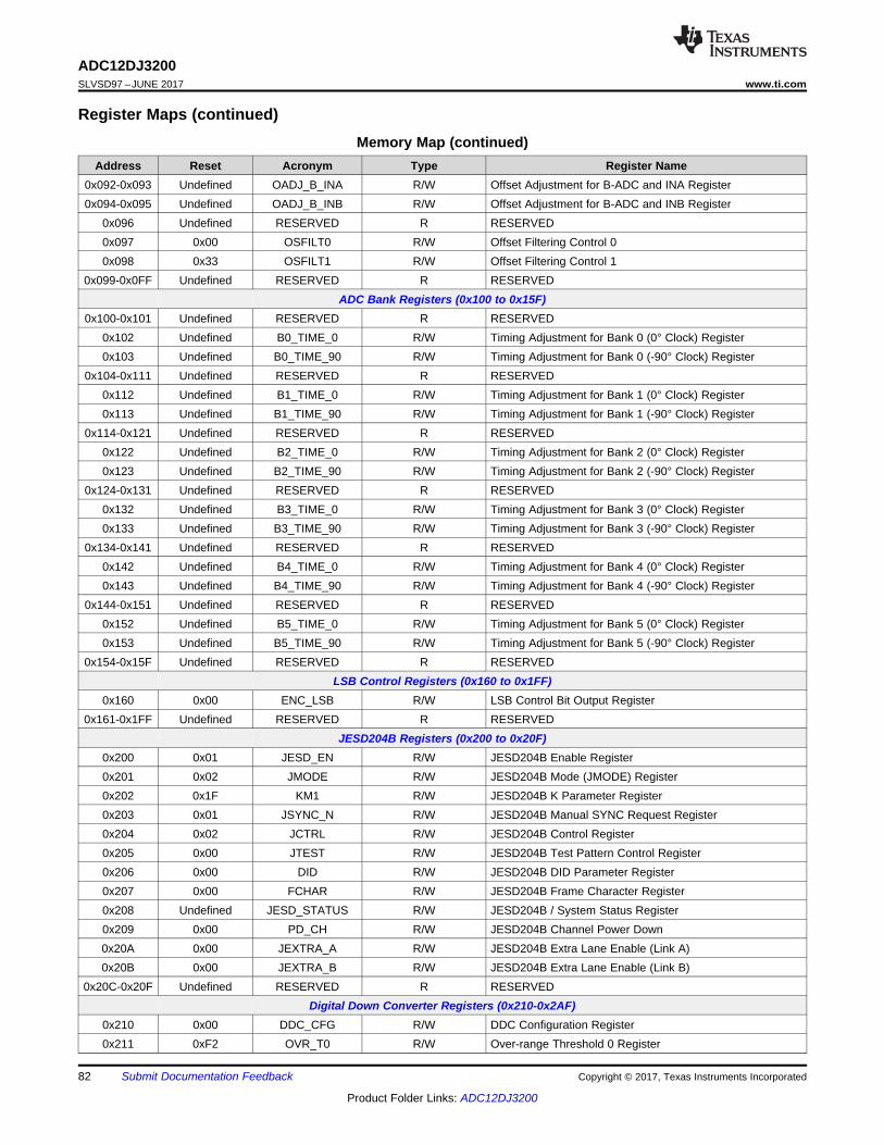
82
ADC12DJ3200SLVSD97 –JUNE 2017 www.ti.com
Product Folder Links: ADC12DJ3200
Submit Documentation Feedback Copyright © 2017, Texas Instruments Incorporated
Register Maps (continued)Memory Map (continued)
Address Reset Acronym Type Register Name0x092-0x093 Undefined OADJ_B_INA R/W Offset Adjustment for B-ADC and INA Register0x094-0x095 Undefined OADJ_B_INB R/W Offset Adjustment for B-ADC and INB Register
0x096 Undefined RESERVED R RESERVED0x097 0x00 OSFILT0 R/W Offset Filtering Control 00x098 0x33 OSFILT1 R/W Offset Filtering Control 1
0x099-0x0FF Undefined RESERVED R RESERVEDADC Bank Registers (0x100 to 0x15F)
0x100-0x101 Undefined RESERVED R RESERVED0x102 Undefined B0_TIME_0 R/W Timing Adjustment for Bank 0 (0° Clock) Register0x103 Undefined B0_TIME_90 R/W Timing Adjustment for Bank 0 (-90° Clock) Register
0x104-0x111 Undefined RESERVED R RESERVED0x112 Undefined B1_TIME_0 R/W Timing Adjustment for Bank 1 (0° Clock) Register0x113 Undefined B1_TIME_90 R/W Timing Adjustment for Bank 1 (-90° Clock) Register
0x114-0x121 Undefined RESERVED R RESERVED0x122 Undefined B2_TIME_0 R/W Timing Adjustment for Bank 2 (0° Clock) Register0x123 Undefined B2_TIME_90 R/W Timing Adjustment for Bank 2 (-90° Clock) Register
0x124-0x131 Undefined RESERVED R RESERVED0x132 Undefined B3_TIME_0 R/W Timing Adjustment for Bank 3 (0° Clock) Register0x133 Undefined B3_TIME_90 R/W Timing Adjustment for Bank 3 (-90° Clock) Register
0x134-0x141 Undefined RESERVED R RESERVED0x142 Undefined B4_TIME_0 R/W Timing Adjustment for Bank 4 (0° Clock) Register0x143 Undefined B4_TIME_90 R/W Timing Adjustment for Bank 4 (-90° Clock) Register
0x144-0x151 Undefined RESERVED R RESERVED0x152 Undefined B5_TIME_0 R/W Timing Adjustment for Bank 5 (0° Clock) Register0x153 Undefined B5_TIME_90 R/W Timing Adjustment for Bank 5 (-90° Clock) Register
0x154-0x15F Undefined RESERVED R RESERVEDLSB Control Registers (0x160 to 0x1FF)
0x160 0x00 ENC_LSB R/W LSB Control Bit Output Register0x161-0x1FF Undefined RESERVED R RESERVED
JESD204B Registers (0x200 to 0x20F)0x200 0x01 JESD_EN R/W JESD204B Enable Register0x201 0x02 JMODE R/W JESD204B Mode (JMODE) Register0x202 0x1F KM1 R/W JESD204B K Parameter Register0x203 0x01 JSYNC_N R/W JESD204B Manual SYNC Request Register0x204 0x02 JCTRL R/W JESD204B Control Register0x205 0x00 JTEST R/W JESD204B Test Pattern Control Register0x206 0x00 DID R/W JESD204B DID Parameter Register0x207 0x00 FCHAR R/W JESD204B Frame Character Register0x208 Undefined JESD_STATUS R/W JESD204B / System Status Register0x209 0x00 PD_CH R/W JESD204B Channel Power Down0x20A 0x00 JEXTRA_A R/W JESD204B Extra Lane Enable (Link A)0x20B 0x00 JEXTRA_B R/W JESD204B Extra Lane Enable (Link B)
0x20C-0x20F Undefined RESERVED R RESERVEDDigital Down Converter Registers (0x210-0x2AF)
0x210 0x00 DDC_CFG R/W DDC Configuration Register0x211 0xF2 OVR_T0 R/W Over-range Threshold 0 Register

83
ADC12DJ3200www.ti.com SLVSD97 –JUNE 2017
Product Folder Links: ADC12DJ3200
Submit Documentation FeedbackCopyright © 2017, Texas Instruments Incorporated
Register Maps (continued)Memory Map (continued)
Address Reset Acronym Type Register Name0x212 0xAB OVR_T1 R/W Over-range Threshold 1 Register0x213 0x07 OVR_CFG R/W Over-range Configuration Register0x214 0x00 CMODE R/W DDC Configuration Preset Mode Register0x215 0x00 CSEL R/W DDC Configuration Preset Select Register0x216 0x02 DIG_BIND R/W Digital Channel Binding Register
0x217-0x218 0x0000 NCO_RDIV R/W Rational NCO Reference Divisor Register0x219 0x02 NCO_SYNC R/W NCO Synchronization Register
0x21A-0x21F Undefined RESERVED R RESERVED0x220-0x223 0xC0000000 FREQA0 R/W NCO Frequency (DDC A Preset 0)0x224-0x225 0x0000 PHASEA0 R/W NCO Phase (DDC A Preset 0)0x226-0x227 Undefined RESERVED R RESERVED0x228-0x22B 0xC0000000 FREQA1 R/W NCO Frequency (DDC A Preset 1)0x22C-0x22D 0x0000 PHASEA1 R/W NCO Phase (DDC A Preset 1)0x22E-0x22F Undefined RESERVED R RESERVED0x230-0x233 0xC0000000 FREQA2 R/W NCO Frequency (DDC A Preset 2)0x234-0x235 0x0000 PHASEA2 R/W NCO Phase (DDC A Preset 2)0x236-0x237 Undefined RESERVED R RESERVED0x238-0x23B 0xC0000000 FREQA3 R/W NCO Frequency (DDC A Preset 3)0x23C-0x23D 0x0000 PHASEA3 R/W NCO Phase (DDC A Preset 3)0x23E-0x23F Undefined RESERVED R RESERVED0x240-0x243 0xC0000000 FREQB0 R/W NCO Frequency (DDC B Preset 0)0x244-0x245 0x0000 PHASEB0 R/W NCO Phase (DDC B Preset 0)0x246-0x247 Undefined RESERVED R RESERVED0x248-0x24B 0xC0000000 FREQB1 R/W NCO Frequency (DDC B Preset 1)0x24C-0x24D 0x0000 PHASEB1 R/W NCO Phase (DDC B Preset 1)0x24E-0x24F Undefined RESERVED R RESERVED0x250-0x253 0xC0000000 FREQB2 R/W NCO Frequency (DDC B Preset 2)0x254-0x255 0x0000 PHASEB2 R/W NCO Phase (DDC B Preset 2)0x256-0x257 Undefined RESERVED R RESERVED0x258-0x25B 0xC0000000 FREQB3 R/W NCO Frequency (DDC B Preset 3)0x25C-0x25D 0x0000 PHASEB3 R/W NCO Phase (DDC B Preset 3)0x25E-0x296 Undefined RESERVED R RESERVED
0x297 Undefined SPIN_ID R Spin Identification Value0x298-0x2AF Undefined RESERVED R RESERVED
SYSREF Calibration Registers (0x2B0 to 0x2BF)0x2B0 0x00 SRC_EN R/W SYSREF Calibration Enable Register0x2B1 0x05 SRC_CFG R/W SYSREF Calibration Configuration Register
0x2B2-0x2B4 Undefined SRC_STATUS R SYSREF Calibration Status0x2B5-0x2B7 0x00 TAD R/W DEVCLK Aperture Delay Adjustment Register
0x2B8 0x00 TAD_RAMP R/W DEVCLK Timing Adjust Ramp Control Register0x2B9-0x2BF Undefined RESERVED R RESERVED
Alarm Registers (0x2C0 to 0x2C2)0x2C0 Undefined ALARM R Alarm Interrupt Status Register0x2C1 0x1F ALM_STATUS R/W Alarm Status Register0x2C2 0x1F ALM_MASK R/W Alarm Mask Register

84
ADC12DJ3200SLVSD97 –JUNE 2017 www.ti.com
Product Folder Links: ADC12DJ3200
Submit Documentation Feedback Copyright © 2017, Texas Instruments Incorporated
7.6.1 Register Descriptions
7.6.1.1 Standard SPI-3.0 (0x000 to 0x00F)
Table 44. Standard SPI-3.0 RegistersAddress Reset Acronym Register Name Section
0x000 0x30 CONFIG_A Configuration A Register Configuration A Register (address =0x000) [reset = 0x30]
0x001 Undefined RESERVED RESERVED
0x002 0x00 DEVICE_CONFIG Device Configuration Register Device Configuration Register (address =0x002) [reset = 0x00]
0x003 0x03 CHIP_TYPE Chip Type Register Chip Type Register (address = 0x003)[reset = 0x03]
0x004-0x005 0x0020 CHIP_ID Chip ID Registers Chip ID Register (address = 0x004 to0x005) [reset = 0x0020]
0x006 0x0A CHIP_VERSION Chip Version Register Chip Version Register (address = 0x006)[reset = 0x01]
0x007-0x00B Undefined RESERVED RESERVED
0x00C-0x00D 0x0451 VENDOR_ID Vendor Identification Register Vendor Identification Register (address =0x00C to 0x00D) [reset = 0x0451]
0x00E-0x00F Undefined RESERVED RESERVED
7.6.1.1.1 Configuration A Register (address = 0x000) [reset = 0x30]
Figure 89. Configuration A Register (CONFIG_A)
7 6 5 4 3 2 1 0SOFT_RESET RESERVED ADDR_ASC SDO_ACTIVE RESERVED
R/W-0 R-0 R/W-1 R-1 R-0000
Table 45. CONFIG_A Field DescriptionsBit Field Type Reset Description7 SOFT_RESET R/W 0 Setting this bit results in full reset of the device. This bit is self-
clearing. After writing this bit, the device may take up to 750 nsto reset. During this time, do not perform any SPI transactions.
6 RESERVED R 0 RESERVED5 ADDR_ASC R/W 1 0: descend – decrement address while streaming reads/writes
1: ascend – increment address while streaming reads/writes(default)
4 SDO_ACTIVE R 1 Always returns 1 indicating that device always uses 4-wire SPImode
3-0 RESERVED R 0000 RESERVED
7.6.1.1.2 Device Configuration Register (address = 0x002) [reset = 0x00]
Figure 90. Device Configuration Register (DEVICE_CONFIG)
7 6 5 4 3 2 1 0RESERVED MODER-0000 00 R/W-00

85
ADC12DJ3200www.ti.com SLVSD97 –JUNE 2017
Product Folder Links: ADC12DJ3200
Submit Documentation FeedbackCopyright © 2017, Texas Instruments Incorporated
Table 46. DEVICE_CONFIG Field DescriptionsBit Field Type Reset Description7-2 RESERVED R 0000 00 RESERVED1-0 MODE R/W 00 SPI 3.0 specification has 1 as low power functional mode, 2 as
low power fast resume and 3 as power-down. This chip does notsupport these modes.0: Normal Operation – full power and full performance (default)1: Normal Operation – full power and full performance2: Power Down - Everything powered down. Only use for briefperiods of time to calibrate on-chip Temperature Diodemeasurement. Please see note beneath RecommendedOperating Conditions for more information.3: Power Down - Everything powered down. Only use for briefperiods of time to calibrate on-chip Temperature Diodemeasurement. Please see note beneath RecommendedOperating Conditions for more information.
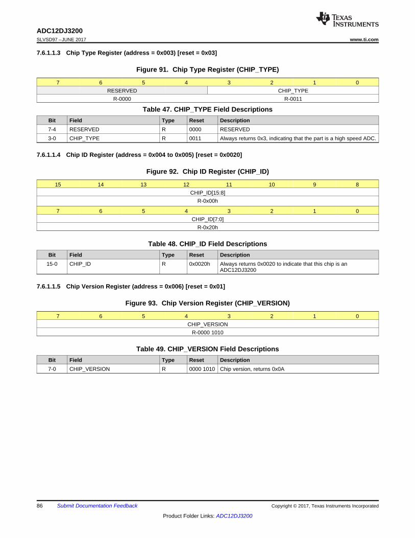
86
ADC12DJ3200SLVSD97 –JUNE 2017 www.ti.com
Product Folder Links: ADC12DJ3200
Submit Documentation Feedback Copyright © 2017, Texas Instruments Incorporated
7.6.1.1.3 Chip Type Register (address = 0x003) [reset = 0x03]
Figure 91. Chip Type Register (CHIP_TYPE)
7 6 5 4 3 2 1 0RESERVED CHIP_TYPE
R-0000 R-0011
Table 47. CHIP_TYPE Field DescriptionsBit Field Type Reset Description7-4 RESERVED R 0000 RESERVED3-0 CHIP_TYPE R 0011 Always returns 0x3, indicating that the part is a high speed ADC.
7.6.1.1.4 Chip ID Register (address = 0x004 to 0x005) [reset = 0x0020]
Figure 92. Chip ID Register (CHIP_ID)
15 14 13 12 11 10 9 8CHIP_ID[15:8]
R-0x00h
7 6 5 4 3 2 1 0CHIP_ID[7:0]
R-0x20h
Table 48. CHIP_ID Field DescriptionsBit Field Type Reset Description
15-0 CHIP_ID R 0x0020h Always returns 0x0020 to indicate that this chip is anADC12DJ3200
7.6.1.1.5 Chip Version Register (address = 0x006) [reset = 0x01]
Figure 93. Chip Version Register (CHIP_VERSION)
7 6 5 4 3 2 1 0CHIP_VERSION
R-0000 1010
Table 49. CHIP_VERSION Field DescriptionsBit Field Type Reset Description7-0 CHIP_VERSION R 0000 1010 Chip version, returns 0x0A

87
ADC12DJ3200www.ti.com SLVSD97 –JUNE 2017
Product Folder Links: ADC12DJ3200
Submit Documentation FeedbackCopyright © 2017, Texas Instruments Incorporated
7.6.1.1.6 Vendor Identification Register (address = 0x00C to 0x00D) [reset = 0x0451]
Figure 94. Vendor Identification Register (VENDOR_ID)
15 14 13 12 11 10 9 8VENDOR_ID[15:8]
R-0x04h
7 6 5 4 3 2 1 0VENDOR_ID[7:0]
R-0x51h
Table 50. VENDOR_ID Field DescriptionsBit Field Type Reset Description
15-0 VENDOR_ID R 0x0451h Always returns 0x0451 (TI Vendor ID)
7.6.1.2 User SPI Configuration (0x010 to 0x01F)
Table 51. User SPI Configuration RegistersAddress Reset Acronym Register Name Section
0x010 0x00 USR0 User SPI Configuration Register User SPI Configuration Register (address= 0x010) [reset = 0x00]
0x011-0x01F Undefined RESERVED RESERVED
7.6.1.2.1 User SPI Configuration Register (address = 0x010) [reset = 0x00]
Figure 95. User SPI Configuration Register (USR0)
7 6 5 4 3 2 1 0RESERVED ADDR_HOLDR-0000 000 R/W-0
Table 52. USR0 Field DescriptionsBit Field Type Reset Description7-1 RESERVED R/W 0000 0000 ADDR_HOLD R/W 0 0: Use ADDR_ASC bit to define what happens to address during
streaming (default).1: Address stays static throughout streaming operation. Usefulfor reading/writing calibration vector information at CAL_DATAregister.

88
ADC12DJ3200SLVSD97 –JUNE 2017 www.ti.com
Product Folder Links: ADC12DJ3200
Submit Documentation Feedback Copyright © 2017, Texas Instruments Incorporated
7.6.1.3 Miscellaneous Analog Registers (0x020 to 0x047)
Table 53. Miscellaneous Analog RegistersAddress Reset Acronym Register Name Section
0x020-0x028 Undefined RESERVED RESERVED
0x029 0x00 CLK_CTRL0 Clock Control Register 0 Clock Control Register 0 (address =0x029) [reset = 0x00]
0x02A 0x20 CLK_CTRL1 Clock Control Register 1 Clock Control Register 1 (address =0x02A) [reset = 0x00]
0x02B Undefined RESERVED RESERVED
0x02C-0x02E Undefined SYSREF_POS SYSREF Capture Position Register SYSREF Capture Position Register(address = 0x02C-0x02E) [reset =
Undefined]
0x02F Undefined RESERVED RESERVED
0x030-0x031 0xA000 FS_RANGE_A INA Full Scale Range Adjust Register INA Full Scale Range Adjust Register(address = 0x030-0x031) [reset =
0xA000]
0x032-0x033 0xA000 FS_RANGE_B INB Full Scale Range Adjust Register INB Full Scale Range Adjust Register(address = 0x032-0x033) [reset =
0xA000]
0x034-0x037 Undefined RESERVED RESERVED
0x038 0x00 BG_BYPASS Internal Reference Bypass Register Internal Reference Bypass Register(address = 0x038) [reset = 0x00]
0x039-0x03A Undefined RESERVED RESERVED
0x03B 0x00 SYNC_CTRL TMSTP+/- Control Register TMSTP+/- Control Register (address =0x03B) [reset = 0x00]
0x03C-0x047 Undefined RESERVED RESERVED
7.6.1.3.1 Clock Control Register 0 (address = 0x029) [reset = 0x00]
Figure 96. Clock Control Register 0 (CLK_CTRL0)
7 6 5 4 3 2 1 0RESERVED SYSREF_PRO
C_ENSYSREF_REC
V_ENSYSREF_ZOO
MSYSREF_SEL
R/W-0 R/W-0 R/W-0 R/W-0 R/W-0000
Table 54. CLK_CTRL0 Field DescriptionsBit Field Type Reset Description7 RESERVED R/W 0 RESERVED6 SYSREF_PROC_EN R/W 0 Enable the SYSREF processor. This must be set to allow the
part to process SYSREF events. SYSREF_RECV_EN must beset before setting SYSREF_PROC_EN.
5 SYSREF_RECV_EN R/W 0 Set this bit to enable the SYSREF receiver circuit4 SYSREF_ZOOM R/W 0 Set this bit to “zoom” in the SYSREF strobe status (impacts
SYSREF_POS)3-0 SYSREF_SEL R/W 0000 Set this field to select which SYSREF delay to use. Set this
based on the results returned by SYSREF_POS. You must setthis to 0 to use SYSREF Calibration.
7.6.1.3.2 Clock Control Register 1 (address = 0x02A) [reset = 0x00]
Figure 97. Clock Control Register 1 (CLK_CTRL1)
7 6 5 4 3 2 1 0RESERVED DEVCLK_LVPE
CL_ENSYSREF_LVPE
CL_ENSYSREF_INVE
RTEDR/W-0010 0 R/W-0 R/W-0 R/W-0

89
ADC12DJ3200www.ti.com SLVSD97 –JUNE 2017
Product Folder Links: ADC12DJ3200
Submit Documentation FeedbackCopyright © 2017, Texas Instruments Incorporated
Table 55. CLK_CTRL1 Field DescriptionsBit Field Type Reset Description7-3 RESERVED R/W 0010 0 RESERVED2 DEVCLK_LVPECL_EN R/W 0 Activate low voltage PECL mode for DEVCLK1 SYSREF_LVPECL_EN R/W 0 Activate low voltage PECL mode for SYSREF0 SYSREF_INVERTED R/W 0 Inverts the SYSREF signal used for alignment

90
ADC12DJ3200SLVSD97 –JUNE 2017 www.ti.com
Product Folder Links: ADC12DJ3200
Submit Documentation Feedback Copyright © 2017, Texas Instruments Incorporated
7.6.1.3.3 SYSREF Capture Position Register (address = 0x02C-0x02E) [reset = Undefined]
Figure 98. SYSREF Capture Position Register (SYSREF_POS)
23 22 21 20 19 18 17 16SYSREF_POS[23:16]
R-Undefined15 14 13 12 11 10 9 8
SYSREF_POS[15:8]R-Undefined
7 6 5 4 3 2 1 0SYSREF_POS[7:0]
R-Undefined
Table 56. SYSREF_POS Field DescriptionsBit Field Type Reset Description
23-0 SYSREF_POS R Undefined Returns a 24-bit status value that indicates the position of theSYSREF edge with respect to DEVCLK. Use this to programSYSREF_SEL.
7.6.1.3.4 INA Full Scale Range Adjust Register (address = 0x030-0x031) [reset = 0xA000]
Figure 99. INA Full Scale Range Adjust Register (FS_RANGE_A)
15 14 13 12 11 10 9 8FS_RANGE_A[15:8]
R/W-0xA0h7 6 5 4 3 2 1 0
FS_RANGE_A[7:0]R/W-0x00h
Table 57. FS_RANGE_A Field DescriptionsBit Field Type Reset Description
15-0 FS_RANGE_A R/W 0xA000h Enables adjustment of the analog full scale range for INA0x0000: Settings below 0x2000 may result in degraded deviceperformance.0x2000: 500 mVpp - Recommended minimum setting.0xA000: 800 mVpp (default)0xFFFF: 1000 mVpp
7.6.1.3.5 INB Full Scale Range Adjust Register (address = 0x032-0x033) [reset = 0xA000]
Figure 100. INB Full Scale Range Adjust Register (FS_RANGE_B)
15 14 13 12 11 10 9 8FS_RANGE_B[15:8]
R/W-0xA07 6 5 4 3 2 1 0
FS_RANGE_B[7:0]R/W-0x00

91
ADC12DJ3200www.ti.com SLVSD97 –JUNE 2017
Product Folder Links: ADC12DJ3200
Submit Documentation FeedbackCopyright © 2017, Texas Instruments Incorporated
Table 58. FS_RANGE_B Field DescriptionsBit Field Type Reset Description
15-0 FS_RANGE_B R/W 0xA000h Enables adjustment of the analog full scale range for INB0x0000: Settings below 0x2000 may result in degraded deviceperformance.0x2000: 500 mVpp - Recommended minimum setting.0xA000: 800 mVpp (default)0xFFFF: 1000 mVpp

92
ADC12DJ3200SLVSD97 –JUNE 2017 www.ti.com
Product Folder Links: ADC12DJ3200
Submit Documentation Feedback Copyright © 2017, Texas Instruments Incorporated
7.6.1.3.6 Internal Reference Bypass Register (address = 0x038) [reset = 0x00]
Figure 101. Internal Reference Bypass Register (BG_BYPASS)
7 6 5 4 3 2 1 0RESERVED BG_BYPASS
R/W-0000 000 R/W-0
Table 59. BG_BYPASS Field DescriptionsBit Field Type Reset Description7-1 RESERVED R/W 0000 000 RESERVED0 BG_BYPASS R/W 0 When set, VA11 is used as the voltage reference instead of the
internal reference
7.6.1.3.7 TMSTP+/- Control Register (address = 0x03B) [reset = 0x00]
Figure 102. TMSTP+/- Control Register (TMSTP_CTRL)
7 6 5 4 3 2 1 0RESERVED TMSTP_LVPE
CL_ENTMSTP_RECV
_ENR/W-0000 00 R/W-0 R/W-0
Table 60. TMSTP_CTRL Field DescriptionsBit Field Type Reset Description7-2 RESERVED R/W 0000 00 RESERVED1 TMSTP_LVPECL_EN R/W 0 When set, activates the low voltage PECL mode for the
differential TMSTP+/- input0 TMSTP_RECV_EN R/W 0 Enables the differential TMSTP+/- input
7.6.1.4 Serializer Registers (0x048 to 0x05F)
Table 61. Serializer RegistersAddress Reset Acronym Register Name Section
0x048 0x00 SER_PE Serializer Pre-Emphasis Control Register
0x049-0x05F Undefined RESERVED RESERVED
7.6.1.4.1 Serializer Pre-Emphasis Control Register (address = 0x048) [reset = 0x00]
Figure 103. Serializer Pre-Emphasis Control Register (SER_PE)
7 6 5 4 3 2 1 0RESERVED SER_PER/W-0000 R/W-0000
Table 62. SER_PE Field DescriptionsBit Field Type Reset Description7-4 RESERVED R/W 0000 RESERVED3-0 SER_PE R/W 0000 Sets the pre-emphasis for the serial lanes to compensate for the
low-pass response of the PCB trace. This is a global setting thataffects all 16 lanes.

93
ADC12DJ3200www.ti.com SLVSD97 –JUNE 2017
Product Folder Links: ADC12DJ3200
Submit Documentation FeedbackCopyright © 2017, Texas Instruments Incorporated
7.6.1.5 Calibration Registers (0x060 to 0x0FF)
Table 63. Calibration RegistersAddress Reset Acronym Register Name Section
0x060 0x01 INPUT_MUX Input Mux Control Register Input Mux Control Register (address =0x060) [reset = 0x01]
0x061 0x01 CAL_EN Calibration Enable Register Calibration Enable Register (address =0x061) [reset = 0x01]
0x062 0x01 CAL_CFG0 Calibration Configuration 0 Register Calibration Configuration 0 Register(address = 0x062) [reset = 0x01]
0x063-0x069 Undefined RESERVED RESERVED
0x06A Undefined CAL_STATUS Calibration Status Register Calibration Status Register (address =0x06A) [reset = Undefined]
0x06B 0x00 CAL_PIN_CFG Calibration Pin Configuration Register Calibration Pin Configuration Register(address = 0x06B) [reset = 0x00]
0x06C 0x01 CAL_SOFT_TRIG Calibration Software Trigger Register Calibration Software Trigger Register(address = 0x06C) [reset = 0x01]
0x06D Undefined RESERVED RESERVED
0x06E 0x88 CAL_LP Low-Power Background Calibration Register Low-Power Background CalibrationRegister (address = 0x06E) [reset =
0x88]
0x06F Undefined RESERVED RESERVED
0x070 0x00 CAL_DATA_EN Calibration Data Enable Register Calibration Data Enable Register(address = 0x070) [reset = 0x00]
0x071 Undefined CAL_DATA Calibration Data Register Calibration Data Register (address =0x071) [reset = Undefined]
0x072-0x079 Undefined RESERVED RESERVED
0x07A Undefined GAIN_TRIM_A Channel A Gain Trim Register Channel A Gain Trim Register (address =0x07A) [reset = Undefined]
0x07B Undefined GAIN_TRIM_B Channel B Gain Trim Register Channel B Gain Trim Register (address =0x07B) [reset = Undefined]
0x07C Undefined BG_TRIM Band-Gap Reference Trim Register Band-Gap Reference Trim Register(address = 0x07C) [reset = Undefined]
0x07D Undefined RESERVED RESERVED
0x07E Undefined RTRIM_A VINA Input Resistor Trim Register VINA Input Resistor Trim Register(address = 0x07E) [reset = Undefined]
0x07F Undefined RTRIM_B VINB Input Resistor Trim Register VINB Input Resistor Trim Register(address = 0x07F) [reset = Undefined]
0x080 Undefined TADJ_A_FG90 Timing Adjustment for A-ADC, Single ChannelMode, Foreground Calibration Register
Timing Adjust for A-ADC, Single ChannelMode, Foreground Calibration Register(address = 0x080) [reset = Undefined]
0x081 Undefined TADJ_B_FG0 Timing Adjustment for B-ADC, Single ChannelMode, Foreground Calibration Register
Timing Adjust for B-ADC, Single ChannelMode, Foreground Calibration Register(address = 0x081) [reset = Undefined]
0x082 Undefined TADJ_A_BG90 Timing Adjustment for A-ADC, Single ChannelMode, Background Calibration Register
Timing Adjust for A-ADC, Single ChannelMode, Background Calibration Register(address = 0x082) [reset = Undefined]
0x083 Undefined TADJ_C_BG0 Timing Adjustment for C-ADC, Single ChannelMode, Background Calibration Register
Timing Adjust for C-ADC, Single ChannelMode, Background Calibration Register(address = 0x084) [reset = Undefined]
0x084 Undefined TADJ_C_BG90 Timing Adjustment for C-ADC, Single ChannelMode, Background Calibration Register
Timing Adjust for C-ADC, Single ChannelMode, Background Calibration Register(address = 0x084) [reset = Undefined]
0x085 Undefined TADJ_B_BG0 Timing Adjustment for B-ADC, Single ChannelMode, Background Calibration Register
Timing Adjust for B-ADC, Single ChannelMode, Background Calibration Register(address = 0x085) [reset = Undefined]
0x086 Undefined TADJ_A Timing Adjustment for A-ADC, Dual ChannelMode Register
Timing Adjust for A-ADC, Dual ChannelMode Register (address = 0x086) [reset
= Undefined]
0x087 Undefined TADJ_CA Timing Adjustment for C-ADC acting for A-ADC, Dual Channel Mode Register
Timing Adjust for C-ADC acting for A-ADC, Dual Channel Mode Register
(address = 0x087) [reset = Undefined]
0x088 Undefined TADJ_CB Timing Adjustment for C-ADC acting for B-ADC, Dual Channel Mode Register
Timing Adjust for C-ADC acting for B-ADC, Dual Channel Mode Register
(address = 0x088) [reset = Undefined]

94
ADC12DJ3200SLVSD97 –JUNE 2017 www.ti.com
Product Folder Links: ADC12DJ3200
Submit Documentation Feedback Copyright © 2017, Texas Instruments Incorporated
Table 63. Calibration Registers (continued)Address Reset Acronym Register Name Section
0x089 Undefined TADJ_B Timing Adjustment for B-ADC, Dual ChannelMode Register
Timing Adjust for B-ADC, Dual ChannelMode Register (address = 0x089) [reset
= Undefined]
0x08A-0x08B Undefined OADJ_A_INA Offset Adjustment for A-ADC and INARegister
Offset Adjustment for A-ADC and INARegister (address = 0x08A-0x08B) [reset
= Undefined]
0x08C-0x08D Undefined OADJ_A_INB Offset Adjustment for A-ADC and INBRegister
Offset Adjustment for A-ADC and INBRegister (address = 0x08C-0x08D) [reset
= Undefined]
0x08E-0x08F Undefined OADJ_C_INA Offset Adjustment for C-ADC and INARegister
Offset Adjustment for C-ADC and INARegister (address = 0x08E-0x08F) [reset
= Undefined]
0x090-0x091 Undefined OADJ_C_INB Offset Adjustment for C-ADC and INBRegister
Offset Adjustment for C-ADC and INBRegister (address = 0x090-0x091) [reset
= Undefined]
0x092-0x093 Undefined OADJ_B_INA Offset Adjustment for B-ADC and INARegister
Offset Adjustment for B-ADC and INARegister (address = 0x092-0x093) [reset
= Undefined]
0x094-0x095 Undefined OADJ_B_INB Offset Adjustment for B-ADC and INBRegister
Offset Adjustment for B-ADC and INBRegister (address = 0x094-0x095) [reset
= Undefined]
0x096 Undefined RESERVED RESERVED
0x097 0x00 0SFILT0 Offset Filtering Control 0 Offset Filtering Control 0 Register(address = 0x097) [reset = 0x00]
0x098 0x33 OSFILT1 Offset Filtering Control 1 Offset Filtering Control 1 Register(address = 0x098) [reset = 0x33]
0x099-0x0FF Undefined RESERVED RESERVED
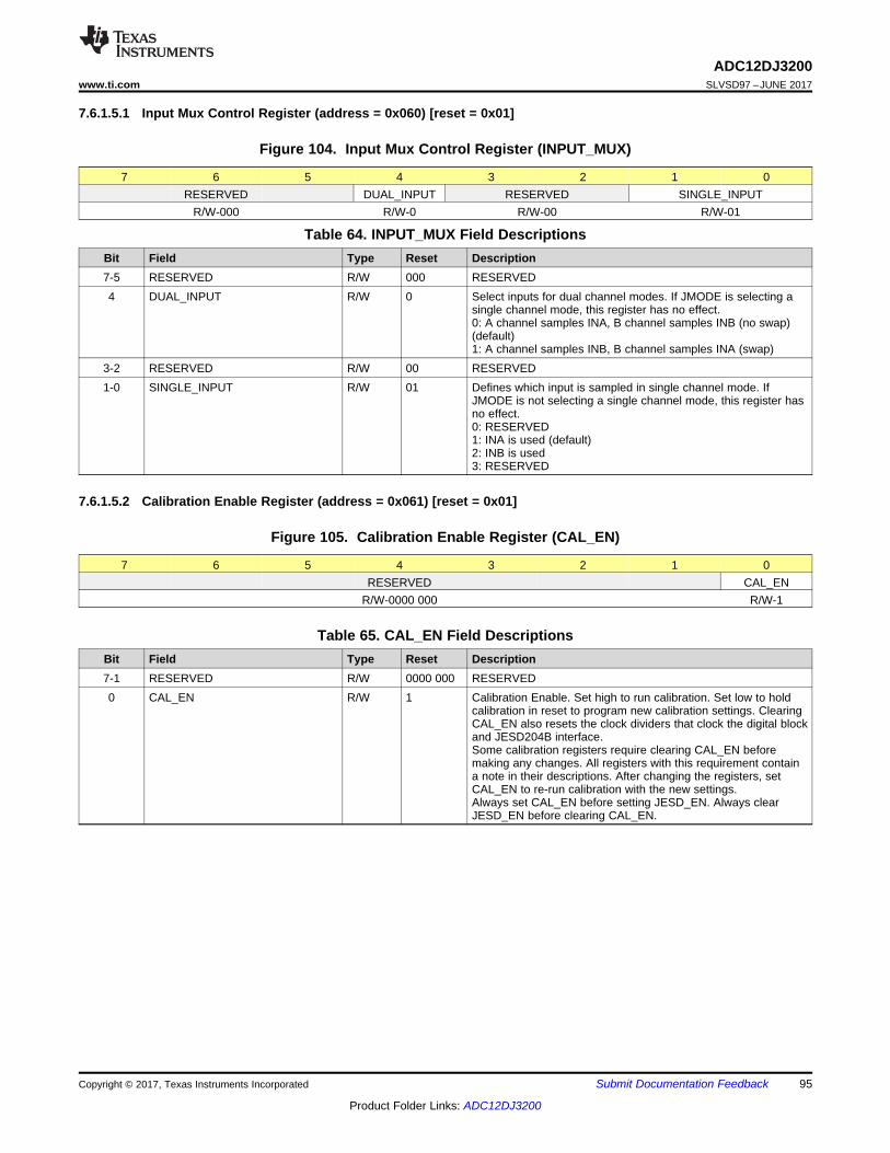
95
ADC12DJ3200www.ti.com SLVSD97 –JUNE 2017
Product Folder Links: ADC12DJ3200
Submit Documentation FeedbackCopyright © 2017, Texas Instruments Incorporated
7.6.1.5.1 Input Mux Control Register (address = 0x060) [reset = 0x01]
Figure 104. Input Mux Control Register (INPUT_MUX)
7 6 5 4 3 2 1 0RESERVED DUAL_INPUT RESERVED SINGLE_INPUT
R/W-000 R/W-0 R/W-00 R/W-01
Table 64. INPUT_MUX Field DescriptionsBit Field Type Reset Description7-5 RESERVED R/W 000 RESERVED4 DUAL_INPUT R/W 0 Select inputs for dual channel modes. If JMODE is selecting a
single channel mode, this register has no effect.0: A channel samples INA, B channel samples INB (no swap)(default)1: A channel samples INB, B channel samples INA (swap)
3-2 RESERVED R/W 00 RESERVED1-0 SINGLE_INPUT R/W 01 Defines which input is sampled in single channel mode. If
JMODE is not selecting a single channel mode, this register hasno effect.0: RESERVED1: INA is used (default)2: INB is used3: RESERVED
7.6.1.5.2 Calibration Enable Register (address = 0x061) [reset = 0x01]
Figure 105. Calibration Enable Register (CAL_EN)
7 6 5 4 3 2 1 0RESERVED CAL_EN
R/W-0000 000 R/W-1
Table 65. CAL_EN Field DescriptionsBit Field Type Reset Description7-1 RESERVED R/W 0000 000 RESERVED0 CAL_EN R/W 1 Calibration Enable. Set high to run calibration. Set low to hold
calibration in reset to program new calibration settings. ClearingCAL_EN also resets the clock dividers that clock the digital blockand JESD204B interface.Some calibration registers require clearing CAL_EN beforemaking any changes. All registers with this requirement containa note in their descriptions. After changing the registers, setCAL_EN to re-run calibration with the new settings.Always set CAL_EN before setting JESD_EN. Always clearJESD_EN before clearing CAL_EN.
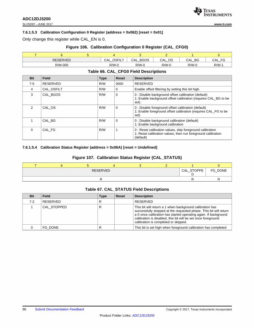
96
ADC12DJ3200SLVSD97 –JUNE 2017 www.ti.com
Product Folder Links: ADC12DJ3200
Submit Documentation Feedback Copyright © 2017, Texas Instruments Incorporated
7.6.1.5.3 Calibration Configuration 0 Register (address = 0x062) [reset = 0x01]
Only change this register while CAL_EN is 0.
Figure 106. Calibration Configuration 0 Register (CAL_CFG0)
7 6 5 4 3 2 1 0RESERVED CAL_OSFILT CAL_BGOS CAL_OS CAL_BG CAL_FG
R/W-000 R/W-0 R/W-0 R/W-0 R/W-0 R/W-1
Table 66. CAL_CFG0 Field DescriptionsBit Field Type Reset Description7-5 RESERVED R/W 0000 RESERVED4 CAL_OSFILT R/W 0 Enable offset filtering by setting this bit high.3 CAL_BGOS R/W 0 0 : Disable background offset calibration (default)
1: Enable background offset calibration (requires CAL_BG to beset).
2 CAL_OS R/W 0 0 : Disable foreground offset calibration (default)1: Enable foreground offset calibration (requires CAL_FG to beset)
1 CAL_BG R/W 0 0 : Disable background calibration (default)1: Enable background calibration
0 CAL_FG R/W 1 0 : Reset calibration values, skip foreground calibration1: Reset calibration values, then run foreground calibration(default)
7.6.1.5.4 Calibration Status Register (address = 0x06A) [reset = Undefined]
Figure 107. Calibration Status Register (CAL_STATUS)
7 6 5 4 3 2 1 0RESERVED CAL_STOPPE
DFG_DONE
R R R
Table 67. CAL_STATUS Field DescriptionsBit Field Type Reset Description7-2 RESERVED R RESERVED1 CAL_STOPPED R This bit will return a 1 when background calibration has
successfully stopped at the requested phase. This bit will returna 0 once calibration has started operating again. If backgroundcalibration is disabled, this bit will be set once foregroundcalibration is completed or skipped.
0 FG_DONE R This bit is set high when foreground calibration has completed

97
ADC12DJ3200www.ti.com SLVSD97 –JUNE 2017
Product Folder Links: ADC12DJ3200
Submit Documentation FeedbackCopyright © 2017, Texas Instruments Incorporated
7.6.1.5.5 Calibration Pin Configuration Register (address = 0x06B) [reset = 0x00]
Figure 108. Calibration Pin Configuration Register (CAL_PIN_CFG)
7 6 5 4 3 2 1 0RESERVED CAL_STATUS_SEL CAL_TRIG_ENR/W-0000 0 R/W-00 R/W-0
Table 68. CAL_PIN_CFG Field DescriptionsBit Field Type Reset Description7-3 RESERVED R/W 0000 0 RESERVED2-1 CAL_STATUS_SEL R/W 00 0: CALSTAT output pin matches FG_DONE
1: RESERVED2: CALSTAT output pin matches ALARM3: CALSTAT output pin is always low.
0 CAL_TRIG_EN R/W 0 Choose hardware or software trigger source0: Use the CAL_SOFT_TRIG register for the calibration trigger.The CAL_TRIG input is disabled (ignored).1: Use the CAL_TRIG input for the calibration trigger. TheCAL_SOFT_TRIG register is ignored.
7.6.1.5.6 Calibration Software Trigger Register (address = 0x06C) [reset = 0x01]
Figure 109. Calibration Software Trigger Register (CAL_SOFT_TRIG)
7 6 5 4 3 2 1 0RESERVED CAL_SOFT_TR
IGR/W-0000 000 R/W-1
Table 69. CAL_SOFT_TRIG Field DescriptionsBit Field Type Reset Description7-1 RESERVED R/W 0000 000 RESERVED0 CAL_SOFT_TRIG R/W 1 CAL_SOFT_TRIG is a software bit to provide the functionality of
the CAL_TRIG input. Program CAL_TRIG_EN=0 to useCAL_SOFT_TRIG for the calibration trigger. Note: If nocalibration trigger is needed, leave CAL_TRIG_EN=0 andCAL_SOFT_TRIG=1 (trigger set high).
7.6.1.5.7 Low-Power Background Calibration Register (address = 0x06E) [reset = 0x88]
Figure 110. Low-Power Background Calibration Register (CAL_LP)
7 6 5 4 3 2 1 0LP_SLEEP_DLY LP_WAKE_DLY RESERVED LP_TRIG LP_EN
R/W-010 R/W-01 R/W-0 R/W-0 R/W-0

98
ADC12DJ3200SLVSD97 –JUNE 2017 www.ti.com
Product Folder Links: ADC12DJ3200
Submit Documentation Feedback Copyright © 2017, Texas Instruments Incorporated
Table 70. CAL_LP Field DescriptionsBit Field Type Reset Description7-5 LP_SLEEP_DLY R/W 010 Adjust how long an ADC sleeps before waking up for calibration
(only applys when LP_EN=1 and LP_TRIG=0). Values below 4are not recommended due to limited overall power reductionbenefits.0: Sleep Delay = (23+1)*256*tDEVCLK1: Sleep Delay = (215+1)*256*tDEVCLK2: Sleep Delay = (218+1)*256*tDEVCLK3: Sleep Delay = (221+1)*256*tDEVCLK4: Sleep Delay = (224+1)*256*tDEVCLK : Default approximately1338ms with 3.2 GHz clock.5: Sleep Delay = (227+1)*256*tDEVCLK6: Sleep Delay = (230+1)*256*tDEVCLK7: Sleep Delay = (233+1)*256*tDEVCLK
4-3 LP_WAKE_DLY R/W 01 Adjust how much time is given up for settling before calibratingan ADC after it wakes up (only applies when LP_EN=1). Valueslower than 1 are not recommended as there will be insufficienttime for the core to stabilize before calibration begins.0:Wake Delay = (23+1)*256*tDEVCLK1: Wake Delay = (218+1)*256*tDEVCLK : Default approximately21ms with 3.2 GHz clock.2: Wake Delay = (221+1)*256*tDEVCLK3: Wake Delay = (224+1)*256*tDEVCLK
2 RESERVED R/W 0 RESERVED1 LP_TRIG R/W 0 0: ADC sleep duration is set by LP_SLEEP_DLY (autonomous
mode).1: ADCs sleep until woken by a trigger. An ADC is awoken whenthe calibration trigger (CAL_SOFT_TRIG bit or CAL_TRIG input)is low.
0 LP_EN R/W 0 0: Disable low-power background calibration (default)1: Enable low-power background calibration (only applies whenCAL_BG=1).
7.6.1.5.8 Calibration Data Enable Register (address = 0x070) [reset = 0x00]
Figure 111. Register (CAL_DATA_EN)
7 6 5 4 3 2 1 0RESERVED CAL_DATA_EN
R/W-0000 000 R/W-0
Table 71. CAL_DATA_EN Field DescriptionsBit Field Type Reset Description7-1 RESERVED R/W 0000 000 RESERVED0 CAL_DATA_EN R/W 0 Set this bit to enable the CAL_DATA register to enable reading
and writing of calibration data. See Calibration Data Read/Writefor more information.
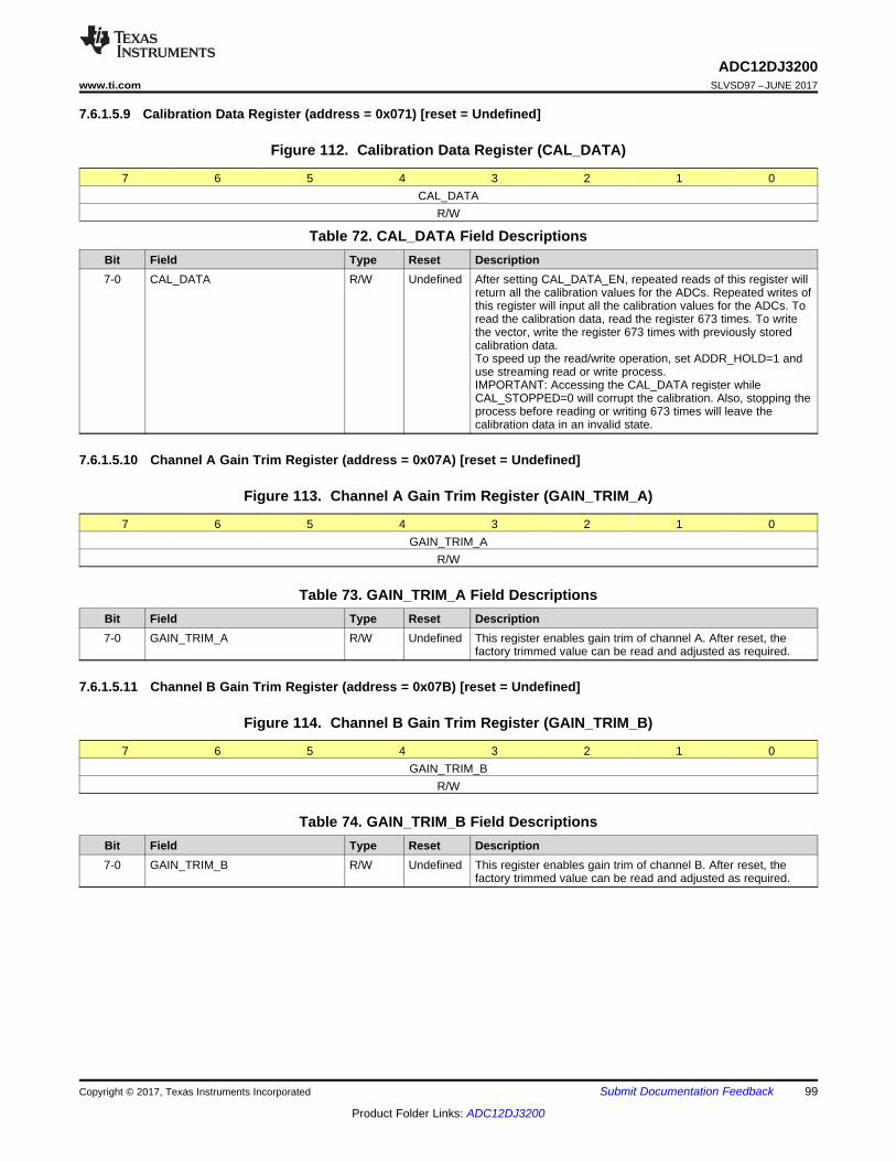
99
ADC12DJ3200www.ti.com SLVSD97 –JUNE 2017
Product Folder Links: ADC12DJ3200
Submit Documentation FeedbackCopyright © 2017, Texas Instruments Incorporated
7.6.1.5.9 Calibration Data Register (address = 0x071) [reset = Undefined]
Figure 112. Calibration Data Register (CAL_DATA)
7 6 5 4 3 2 1 0CAL_DATA
R/W
Table 72. CAL_DATA Field DescriptionsBit Field Type Reset Description7-0 CAL_DATA R/W Undefined After setting CAL_DATA_EN, repeated reads of this register will
return all the calibration values for the ADCs. Repeated writes ofthis register will input all the calibration values for the ADCs. Toread the calibration data, read the register 673 times. To writethe vector, write the register 673 times with previously storedcalibration data.To speed up the read/write operation, set ADDR_HOLD=1 anduse streaming read or write process.IMPORTANT: Accessing the CAL_DATA register whileCAL_STOPPED=0 will corrupt the calibration. Also, stopping theprocess before reading or writing 673 times will leave thecalibration data in an invalid state.
7.6.1.5.10 Channel A Gain Trim Register (address = 0x07A) [reset = Undefined]
Figure 113. Channel A Gain Trim Register (GAIN_TRIM_A)
7 6 5 4 3 2 1 0GAIN_TRIM_A
R/W
Table 73. GAIN_TRIM_A Field DescriptionsBit Field Type Reset Description7-0 GAIN_TRIM_A R/W Undefined This register enables gain trim of channel A. After reset, the
factory trimmed value can be read and adjusted as required.
7.6.1.5.11 Channel B Gain Trim Register (address = 0x07B) [reset = Undefined]
Figure 114. Channel B Gain Trim Register (GAIN_TRIM_B)
7 6 5 4 3 2 1 0GAIN_TRIM_B
R/W
Table 74. GAIN_TRIM_B Field DescriptionsBit Field Type Reset Description7-0 GAIN_TRIM_B R/W Undefined This register enables gain trim of channel B. After reset, the
factory trimmed value can be read and adjusted as required.

100
ADC12DJ3200SLVSD97 –JUNE 2017 www.ti.com
Product Folder Links: ADC12DJ3200
Submit Documentation Feedback Copyright © 2017, Texas Instruments Incorporated
7.6.1.5.12 Band-Gap Reference Trim Register (address = 0x07C) [reset = Undefined]
Figure 115. Band-Gap Reference Trim Register (BG_TRIM)
7 6 5 4 3 2 1 0RESERVED BG_TRIMR/W-0000 R/W
Table 75. BG_TRIM Field DescriptionsBit Field Type Reset Description7-4 RESERVED R/W 0000 RESERVED3-0 BG_TRIM R/W Undefined This register enables trim of the internal band-gap reference.
After reset, the factory trimmed value can be read and adjustedas required.
7.6.1.5.13 VINA Input Resistor Trim Register (address = 0x07E) [reset = Undefined]
Figure 116. VINA Input Resistor Trim Register (RTRIM_A)
7 6 5 4 3 2 1 0RTRIM
R/W
Table 76. RTRIM_A Field DescriptionsBit Field Type Reset Description7-0 RTRIM_A R/W Undefined This register controls VINA ADC input termination trim. After
reset, the factory trimmed value can be read and adjusted asrequired.
7.6.1.5.14 VINB Input Resistor Trim Register (address = 0x07F) [reset = Undefined]
Figure 117. VINB Input Resistor Trim Register (RTRIM_B)
7 6 5 4 3 2 1 0RTRIM
R/W
Table 77. RTRIM_B Field DescriptionsBit Field Type Reset Description7-0 RTRIM_B R/W Undefined This register controls VINB ADC input termination trim. After
reset, the factory trimmed value can be read and adjusted asrequired.
7.6.1.5.15 Timing Adjust for A-ADC, Single Channel Mode, Foreground Calibration Register (address = 0x080) [reset= Undefined]
Figure 118. Register (TADJ_A_FG90)
7 6 5 4 3 2 1 0TADJ_A_FG90
R/W

101
ADC12DJ3200www.ti.com SLVSD97 –JUNE 2017
Product Folder Links: ADC12DJ3200
Submit Documentation FeedbackCopyright © 2017, Texas Instruments Incorporated
Table 78. TADJ_A_FG90 Field DescriptionsBit Field Type Reset Description7-0 TADJ_A_FG90 R/W Undefined This register (and other TADJ* registers that follow it) are used
to adjust the sampling instant of each ADC core. Different TADJregisters apply to different ADCs under different modes orphases of background calibration. After reset, the factorytrimmed value can be read and adjusted as required.
7.6.1.5.16 Timing Adjust for B-ADC, Single Channel Mode, Foreground Calibration Register (address = 0x081) [reset= Undefined]
Figure 119. Register (TADJ_B_FG0)
7 6 5 4 3 2 1 0TADJ_B_FG0
R/W
Table 79. TADJ_B_FG0 Field DescriptionsBit Field Type Reset Description7-0 TADJ_B_FG0 R/W Undefined This register (and other TADJ* registers that follow it) are used
to adjust the sampling instant of each ADC core. Different TADJregisters apply to different ADCs under different modes orphases of background calibration. After reset, the factorytrimmed value can be read and adjusted as required.

102
ADC12DJ3200SLVSD97 –JUNE 2017 www.ti.com
Product Folder Links: ADC12DJ3200
Submit Documentation Feedback Copyright © 2017, Texas Instruments Incorporated
7.6.1.5.17 Timing Adjust for A-ADC, Single Channel Mode, Background Calibration Register (address = 0x082)[reset = Undefined]
Figure 120. Register (TADJ_A_BG90)
7 6 5 4 3 2 1 0TADJ_A_BG90
R/W
Table 80. TADJ_B_FG0 Field DescriptionsBit Field Type Reset Description7-0 TADJ_A_BG90 R/W Undefined This register (and other TADJ* registers that follow it) are used
to adjust the sampling instant of each ADC core. Different TADJregisters apply to different ADCs under different modes orphases of background calibration. After reset, the factorytrimmed value can be read and adjusted as required.
7.6.1.5.18 Timing Adjust for C-ADC, Single Channel Mode, Background Calibration Register (address = 0x083)[reset = Undefined]
Figure 121. Register (TADJ_C_BG0)
7 6 5 4 3 2 1 0TADJ_C_BG0
R/W
Table 81. TADJ_B_FG0 Field DescriptionsBit Field Type Reset Description7-0 TADJ_C_BG0 R/W Undefined This register (and other TADJ* registers that follow it) are used
to adjust the sampling instant of each ADC core. Different TADJregisters apply to different ADCs under different modes orphases of background calibration. After reset, the factorytrimmed value can be read and adjusted as required.
7.6.1.5.19 Timing Adjust for C-ADC, Single Channel Mode, Background Calibration Register (address = 0x084)[reset = Undefined]
Figure 122. Register (TADJ_C_BG90)
7 6 5 4 3 2 1 0TADJ_C_BG90
R/W
Table 82. TADJ_B_FG0 Field DescriptionsBit Field Type Reset Description7-0 TADJ_C_BG90 R/W Undefined This register (and other TADJ* registers that follow it) are used
to adjust the sampling instant of each ADC core. Different TADJregisters apply to different ADCs under different modes orphases of background calibration. After reset, the factorytrimmed value can be read and adjusted as required.

103
ADC12DJ3200www.ti.com SLVSD97 –JUNE 2017
Product Folder Links: ADC12DJ3200
Submit Documentation FeedbackCopyright © 2017, Texas Instruments Incorporated
7.6.1.5.20 Timing Adjust for B-ADC, Single Channel Mode, Background Calibration Register (address = 0x085)[reset = Undefined]
Figure 123. Register (TADJ_B_BG0)
7 6 5 4 3 2 1 0TADJ_B_BG0
R/W
Table 83. TADJ_B_FG0 Field DescriptionsBit Field Type Reset Description7-0 TADJ_B_BG0 R/W Undefined This register (and other TADJ* registers that follow it) are used
to adjust the sampling instant of each ADC core. Different TADJregisters apply to different ADCs under different modes orphases of background calibration. After reset, the factorytrimmed value can be read and adjusted as required.
7.6.1.5.21 Timing Adjust for A-ADC, Dual Channel Mode Register (address = 0x086) [reset = Undefined]
Figure 124. Register (TADJ_A)
7 6 5 4 3 2 1 0TADJ_A
R/W
Table 84. TADJ_A Field DescriptionsBit Field Type Reset Description7-0 TADJ_A R/W Undefined This register (and other TADJ* registers that follow it) are used
to adjust the sampling instant of each ADC core. Different TADJregisters apply to different ADCs under different modes orphases of background calibration. After reset, the factorytrimmed value can be read and adjusted as required.
7.6.1.5.22 Timing Adjust for C-ADC acting for A-ADC, Dual Channel Mode Register (address = 0x087) [reset =Undefined]
Figure 125. Register (TADJ_CA)
7 6 5 4 3 2 1 0TADJ_CA
R/W
Table 85. TADJ_CA Field DescriptionsBit Field Type Reset Description7-0 TADJ_CA R/W Undefined This register (and other TADJ* registers that follow it) are used
to adjust the sampling instant of each ADC core. Different TADJregisters apply to different ADCs under different modes orphases of background calibration. After reset, the factorytrimmed value can be read and adjusted as required.

104
ADC12DJ3200SLVSD97 –JUNE 2017 www.ti.com
Product Folder Links: ADC12DJ3200
Submit Documentation Feedback Copyright © 2017, Texas Instruments Incorporated
7.6.1.5.23 Timing Adjust for C-ADC acting for B-ADC, Dual Channel Mode Register (address = 0x088) [reset =Undefined]
Figure 126. Register (TADJ_CB)
7 6 5 4 3 2 1 0TADJ_CB
R/W
Table 86. TADJ_CB Field DescriptionsBit Field Type Reset Description7-0 TADJ_CB R/W Undefined This register (and other TADJ* registers that follow it) are used
to adjust the sampling instant of each ADC core. Different TADJregisters apply to different ADCs under different modes orphases of background calibration. After reset, the factorytrimmed value can be read and adjusted as required.
7.6.1.5.24 Timing Adjust for B-ADC, Dual Channel Mode Register (address = 0x089) [reset = Undefined]
Figure 127. Register (TADJ_B)
7 6 5 4 3 2 1 0TADJ_B
R/W
Table 87. TADJ_B Field DescriptionsBit Field Type Reset Description7-0 TADJ_B R/W Undefined This register (and other TADJ* registers that follow it) are used
to adjust the sampling instant of each ADC core. Different TADJregisters apply to different ADCs under different modes orphases of background calibration. After reset, the factorytrimmed value can be read and adjusted as required.
7.6.1.5.25 Offset Adjustment for A-ADC and INA Register (address = 0x08A-0x08B) [reset = Undefined]
Figure 128. Register (OADJ_A_INA)
15 14 13 12 11 10 9 8RESERVED OADJ_A_INA[11:8]R/W-0000 R/W
7 6 5 4 3 2 1 0OADJ_A_INA[7:0]
R/W
Table 88. OADJ_A_INA Field DescriptionsBit Field Type Reset Description
15-12 RESERVED R/W 0000 RESERVED11-0 OADJ_A_INA R/W Undefined Offset adjustment value for ADC0 (A-ADC) applied when ADC0
samples INA. The format is unsigned. After reset, the factorytrimmed value can be read and adjusted as required.Important notes:• Never write OADJ* registers while foreground calibration is
underway• Never write OADJ* registers if CAL_BG and CAL_BGOS
are set• If CAL_OS=1 and CAL_BGOS=0, only read OADJ* registers
if FG_DONE=1• If CAL_BG=1 and CAL_BGOS=1, only read OADJ* register
if CAL_STOPPED=1

105
ADC12DJ3200www.ti.com SLVSD97 –JUNE 2017
Product Folder Links: ADC12DJ3200
Submit Documentation FeedbackCopyright © 2017, Texas Instruments Incorporated
7.6.1.5.26 Offset Adjustment for A-ADC and INB Register (address = 0x08C-0x08D) [reset = Undefined]
Figure 129. Register (OADJ_A_INB)
15 14 13 12 11 10 9 8RESERVED OADJ_A_INB[11:8]R/W-0000 R/W
7 6 5 4 3 2 1 0OADJ_A_INB[7:0]
R/W
Table 89. OADJ_A_INB Field DescriptionsBit Field Type Reset Description
15-12 RESERVED R/W 0000 RESERVED11-0 OADJ_A_INB R/W Undefined Offset adjustment value for ADC0 (A-ADC) applied when ADC0
samples INB. The format is unsigned. After reset, the factorytrimmed value can be read and adjusted as required.Important notes:• Never write OADJ* registers while foreground calibration is
underway• Never write OADJ* registers if CAL_BG and CAL_BGOS
are set• If CAL_OS=1 and CAL_BGOS=0, only read OADJ* registers
if FG_DONE=1• If CAL_BG=1 and CAL_BGOS=1, only read OADJ* register
if CAL_STOPPED=1
7.6.1.5.27 Offset Adjustment for C-ADC and INA Register (address = 0x08E-0x08F) [reset = Undefined]
Figure 130. Register (OADJ_C_INA)
15 14 13 12 11 10 9 8RESERVED OADJ_C_INA[11:8]R/W-0000 R/W
7 6 5 4 3 2 1 0OADJ_C_INA[7:0]
R/W
Table 90. OADJ_C_INA Field DescriptionsBit Field Type Reset Description
15-12 RESERVED R/W 0000 RESERVED11-0 OADJ_C_INA R/W Undefined Offset adjustment value for ADC1 (A-ADC) applied when ADC1
samples INA. The format is unsigned. After reset, the factorytrimmed value can be read and adjusted as required.Important notes:• Never write OADJ* registers while foreground calibration is
underway• Never write OADJ* registers if CAL_BG and CAL_BGOS
are set• If CAL_OS=1 and CAL_BGOS=0, only read OADJ* registers
if FG_DONE=1• If CAL_BG=1 and CAL_BGOS=1, only read OADJ* register
if CAL_STOPPED=1
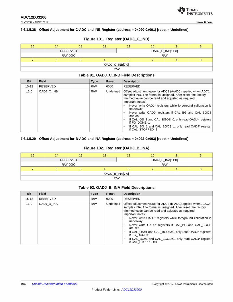
106
ADC12DJ3200SLVSD97 –JUNE 2017 www.ti.com
Product Folder Links: ADC12DJ3200
Submit Documentation Feedback Copyright © 2017, Texas Instruments Incorporated
7.6.1.5.28 Offset Adjustment for C-ADC and INB Register (address = 0x090-0x091) [reset = Undefined]
Figure 131. Register (OADJ_C_INB)
15 14 13 12 11 10 9 8RESERVED OADJ_C_INB[11:8]R/W-0000 R/W
7 6 5 4 3 2 1 0OADJ_C_INB[7:0]
R/W
Table 91. OADJ_C_INB Field DescriptionsBit Field Type Reset Description
15-12 RESERVED R/W 0000 RESERVED11-0 OADJ_C_INB R/W Undefined Offset adjustment value for ADC1 (A-ADC) applied when ADC1
samples INB. The format is unsigned. After reset, the factorytrimmed value can be read and adjusted as required.Important notes:• Never write OADJ* registers while foreground calibration is
underway• Never write OADJ* registers if CAL_BG and CAL_BGOS
are set• If CAL_OS=1 and CAL_BGOS=0, only read OADJ* registers
if FG_DONE=1• If CAL_BG=1 and CAL_BGOS=1, only read OADJ* register
if CAL_STOPPED=1
7.6.1.5.29 Offset Adjustment for B-ADC and INA Register (address = 0x092-0x093) [reset = Undefined]
Figure 132. Register (OADJ_B_INA)
15 14 13 12 11 10 9 8RESERVED OADJ_B_INA[11:8]R/W-0000 R/W
7 6 5 4 3 2 1 0OADJ_B_INA[7:0]
R/W
Table 92. OADJ_B_INA Field DescriptionsBit Field Type Reset Description
15-12 RESERVED R/W 0000 RESERVED11-0 OADJ_B_INA R/W Undefined Offset adjustment value for ADC2 (B-ADC) applied when ADC2
samples INA. The format is unsigned. After reset, the factorytrimmed value can be read and adjusted as required.Important notes:• Never write OADJ* registers while foreground calibration is
underway• Never write OADJ* registers if CAL_BG and CAL_BGOS
are set• If CAL_OS=1 and CAL_BGOS=0, only read OADJ* registers
if FG_DONE=1• If CAL_BG=1 and CAL_BGOS=1, only read OADJ* register
if CAL_STOPPED=1

107
ADC12DJ3200www.ti.com SLVSD97 –JUNE 2017
Product Folder Links: ADC12DJ3200
Submit Documentation FeedbackCopyright © 2017, Texas Instruments Incorporated
7.6.1.5.30 Offset Adjustment for B-ADC and INB Register (address = 0x094-0x095) [reset = Undefined]
Figure 133. Register (OADJ_B_INB)
15 14 13 12 11 10 9 8RESERVED OADJ_B_INB[11:8]R/W-0000 R/W
7 6 5 4 3 2 1 0OADJ_B_INB[7:0]
R/W
Table 93. OADJ_B_INB Field DescriptionsBit Field Type Reset Description
15-12 RESERVED R/W 0000 RESERVED11-0 OADJ_B_INB R/W Undefined Offset adjustment value for ADC2 (B-ADC) applied when ADC2
samples INB. The format is unsigned. After reset, the factorytrimmed value can be read and adjusted as required.Important notes:• Never write OADJ* registers while foreground calibration is
underway• Never write OADJ* registers if CAL_BG and CAL_BGOS
are set• If CAL_OS=1 and CAL_BGOS=0, only read OADJ* registers
if FG_DONE=1• If CAL_BG=1 and CAL_BGOS=1, only read OADJ* register
if CAL_STOPPED=1
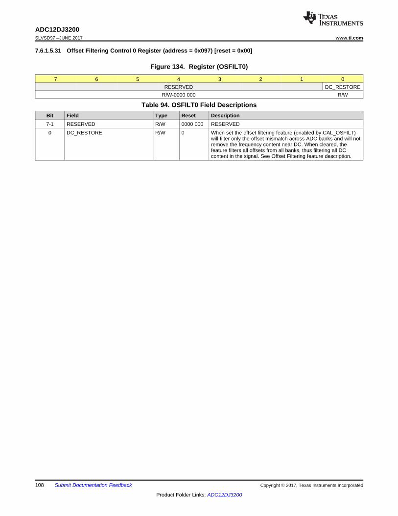
108
ADC12DJ3200SLVSD97 –JUNE 2017 www.ti.com
Product Folder Links: ADC12DJ3200
Submit Documentation Feedback Copyright © 2017, Texas Instruments Incorporated
7.6.1.5.31 Offset Filtering Control 0 Register (address = 0x097) [reset = 0x00]
Figure 134. Register (OSFILT0)
7 6 5 4 3 2 1 0RESERVED DC_RESTORE
R/W-0000 000 R/W
Table 94. OSFILT0 Field DescriptionsBit Field Type Reset Description7-1 RESERVED R/W 0000 000 RESERVED0 DC_RESTORE R/W 0 When set the offset filtering feature (enabled by CAL_OSFILT)
will filter only the offset mismatch across ADC banks and will notremove the frequency content near DC. When cleared, thefeature filters all offsets from all banks, thus filtering all DCcontent in the signal. See Offset Filtering feature description.

109
ADC12DJ3200www.ti.com SLVSD97 –JUNE 2017
Product Folder Links: ADC12DJ3200
Submit Documentation FeedbackCopyright © 2017, Texas Instruments Incorporated
7.6.1.5.32 Offset Filtering Control 1 Register (address = 0x098) [reset = 0x33]
Figure 135. Register (OSFILT1)
7 6 5 4 3 2 1 0OSFILT_BW OSFILT_SOAK
R/W-0011 R/W-0011
Table 95. OSFILT1 Field DescriptionsBit Field Type Reset Description7-4 OSFILT_BW R/W 0011 This adjusts the IIR filter bandwidth for the offset filtering feature
(enabled by CAL_OSFILT). More bandwidth will suppress moreflicker noise from the ADCs and reduce the offset spurs. Lessbandwidth will minimize the impact of the filters on the missionmode signal.OSFILT_BW: IIR Coefficient: -3dB Bandwidth (single sided)0: RESERVED: RESERVED1: 2-10 : 609e-9*FDEVCLK2: 2-11 : 305e-9*FDEVCLK3: 2-12 : 152e-9*FDEVCLK4: 2-13 : 76e-9*FDEVCLK5: 2-14 : 38e-9*FDEVCLK6-15: RESERVED
3-0 OSFILT_SOAK R/W 0011 This adjusts the IIR soak time for the offset filtering feature. Thisapplies when offset filtering and background calibration are bothenabled. This field determines how long the IIR filter is allowedto settle when it is first connected to an ADC after the ADC iscalibrated. After the soak time completes, the ADC is placedonline using the IIR filter. It is recommended to setOSFILT_SOAK = OSFILT_BW.
7.6.1.6 ADC Bank Registers (0x100 to 0x15F)
Table 96. ADC Bank RegistersAddress Reset Acronym Register Name Section
0x100-0x101 Undefined RESERVED RESERVED
0x102 Undefined B0_TIME_0 Timing Adjustment for Bank 0 (0° Clock) Register Timing Adjustment for Bank 0(0° Clock) Register (address =
0x102) [reset = Undefined]
0x103 Undefined B0_TIME_90 Timing Adjustment for Bank 0 (-90° Clock) Register Timing Adjustment for Bank 0(-90° Clock) Register (address= 0x103) [reset = Undefined]
0x104-0x111 Undefined RESERVED RESERVED
0x112 Undefined B1_TIME_0 Timing Adjustment for Bank 1 (0° Clock) Register Timing Adjustment for Bank 1(0° Clock) Register (address =
0x112) [reset = Undefined]
0x113 Undefined B1_TIME_90 Timing Adjustment for Bank 1 (-90° Clock) Register Timing Adjustment for Bank 1(-90° Clock) Register (address= 0x113) [reset = Undefined]
0x114-0x121 Undefined RESERVED RESERVED
0x122 Undefined B2_TIME_0 Timing Adjustment for Bank 2 (0° Clock) Register Timing Adjustment for Bank 2(0° Clock) Register (address =
0x122) [reset = Undefined]
0x123 Undefined B2_TIME_90 Timing Adjustment for Bank 2 (-90° Clock) Register Timing Adjustment for Bank 2(-90° Clock) Register (address= 0x123) [reset = Undefined]
0x124-0x131 Undefined RESERVED RESERVED
0x132 Undefined B3_TIME_0 Timing Adjustment for Bank 3 (0° Clock) Register Timing Adjustment for Bank 3(0° Clock) Register (address =
0x132) [reset = Undefined]
0x133 Undefined B3_TIME_90 Timing Adjustment for Bank 3 (-90° Clock) Register Timing Adjustment for Bank 3(-90° Clock) Register (address= 0x133) [reset = Undefined]
0x134-0x141 Undefined RESERVED RESERVED
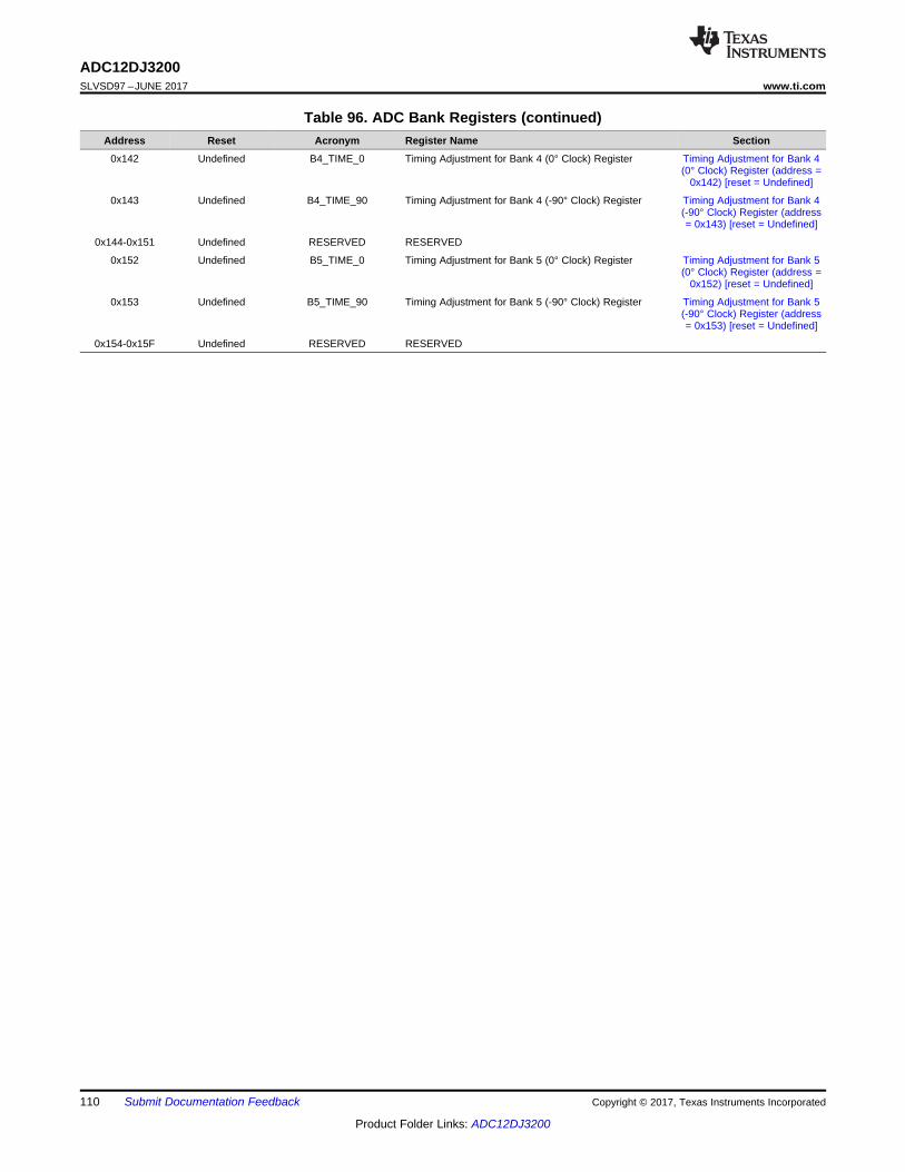
110
ADC12DJ3200SLVSD97 –JUNE 2017 www.ti.com
Product Folder Links: ADC12DJ3200
Submit Documentation Feedback Copyright © 2017, Texas Instruments Incorporated
Table 96. ADC Bank Registers (continued)Address Reset Acronym Register Name Section
0x142 Undefined B4_TIME_0 Timing Adjustment for Bank 4 (0° Clock) Register Timing Adjustment for Bank 4(0° Clock) Register (address =
0x142) [reset = Undefined]
0x143 Undefined B4_TIME_90 Timing Adjustment for Bank 4 (-90° Clock) Register Timing Adjustment for Bank 4(-90° Clock) Register (address= 0x143) [reset = Undefined]
0x144-0x151 Undefined RESERVED RESERVED
0x152 Undefined B5_TIME_0 Timing Adjustment for Bank 5 (0° Clock) Register Timing Adjustment for Bank 5(0° Clock) Register (address =
0x152) [reset = Undefined]
0x153 Undefined B5_TIME_90 Timing Adjustment for Bank 5 (-90° Clock) Register Timing Adjustment for Bank 5(-90° Clock) Register (address= 0x153) [reset = Undefined]
0x154-0x15F Undefined RESERVED RESERVED

111
ADC12DJ3200www.ti.com SLVSD97 –JUNE 2017
Product Folder Links: ADC12DJ3200
Submit Documentation FeedbackCopyright © 2017, Texas Instruments Incorporated
7.6.1.6.1 Timing Adjustment for Bank 0 (0° Clock) Register (address = 0x102) [reset = Undefined]
Figure 136. Timing Adjustment for Bank 0 (0° Clock) Register (B0_TIME_0)
7 6 5 4 3 2 1 0B0_TIME_0
R/W
Table 97. B0_TIME_0 Field DescriptionsBit Field Type Reset Description7-0 B0_TIME_0 R/W Undefined Time adjustment for bank 0 (applied when ADC is configured for
0° clock phase). After reset, the factory trimmed value can beread and adjusted as required.
7.6.1.6.2 Timing Adjustment for Bank 0 (-90° Clock) Register (address = 0x103) [reset = Undefined]
Figure 137. Timing Adjustment for Bank 0 (-90° Clock) Register (B0_TIME_90)
7 6 5 4 3 2 1 0B0_TIME_90
R/W
Table 98. B0_TIME_90 Field DescriptionsBit Field Type Reset Description7-0 B0_TIME_90 R/W Undefined Time adjustment for bank 0 (applied when ADC is configured for
-90° clock phase). After reset, the factory trimmed value can beread and adjusted as required.
7.6.1.6.3 Timing Adjustment for Bank 1 (0° Clock) Register (address = 0x112) [reset = Undefined]
Figure 138. Timing Adjustment for Bank 1 (0° Clock) Register (B1_TIME_0)
7 6 5 4 3 2 1 0B1_TIME_0
R/W
Table 99. B1_TIME_0 Field DescriptionsBit Field Type Reset Description7-0 B1_TIME_0 R/W Undefined Time adjustment for bank 1 (applied when ADC is configured for
0° clock phase). After reset, the factory trimmed value can beread and adjusted as required.
7.6.1.6.4 Timing Adjustment for Bank 1 (-90° Clock) Register (address = 0x113) [reset = Undefined]
Figure 139. Timing Adjustment for Bank 1 (-90° Clock) Register (B1_TIME_90)
7 6 5 4 3 2 1 0B1_TIME_90
R/W
Table 100. B1_TIME_90 Field DescriptionsBit Field Type Reset Description7-0 B1_TIME_90 R/W Undefined Time adjustment for bank 1 (applied when ADC is configured for
-90° clock phase). After reset, the factory trimmed value can beread and adjusted as required.
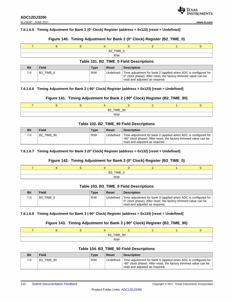
112
ADC12DJ3200SLVSD97 –JUNE 2017 www.ti.com
Product Folder Links: ADC12DJ3200
Submit Documentation Feedback Copyright © 2017, Texas Instruments Incorporated
7.6.1.6.5 Timing Adjustment for Bank 2 (0° Clock) Register (address = 0x122) [reset = Undefined]
Figure 140. Timing Adjustment for Bank 2 (0° Clock) Register (B2_TIME_0)
7 6 5 4 3 2 1 0B2_TIME_0
R/W
Table 101. B2_TIME_0 Field DescriptionsBit Field Type Reset Description7-0 B2_TIME_0 R/W Undefined Time adjustment for bank 2 (applied when ADC is configured for
0° clock phase). After reset, the factory trimmed value can beread and adjusted as required.
7.6.1.6.6 Timing Adjustment for Bank 2 (-90° Clock) Register (address = 0x123) [reset = Undefined]
Figure 141. Timing Adjustment for Bank 2 (-90° Clock) Register (B2_TIME_90)
7 6 5 4 3 2 1 0B2_TIME_90
R/W
Table 102. B2_TIME_90 Field DescriptionsBit Field Type Reset Description7-0 B2_TIME_90 R/W Undefined Time adjustment for bank 2 (applied when ADC is configured for
-90° clock phase). After reset, the factory trimmed value can beread and adjusted as required.
7.6.1.6.7 Timing Adjustment for Bank 3 (0° Clock) Register (address = 0x132) [reset = Undefined]
Figure 142. Timing Adjustment for Bank 3 (0° Clock) Register (B3_TIME_0)
7 6 5 4 3 2 1 0B3_TIME_0
R/W
Table 103. B3_TIME_0 Field DescriptionsBit Field Type Reset Description7-0 B3_TIME_0 R/W Undefined Time adjustment for bank 3 (applied when ADC is configured for
0° clock phase). After reset, the factory trimmed value can beread and adjusted as required.
7.6.1.6.8 Timing Adjustment for Bank 3 (-90° Clock) Register (address = 0x133) [reset = Undefined]
Figure 143. Timing Adjustment for Bank 3 (-90° Clock) Register (B3_TIME_90)
7 6 5 4 3 2 1 0B3_TIME_90
R/W
Table 104. B3_TIME_90 Field DescriptionsBit Field Type Reset Description7-0 B3_TIME_90 R/W Undefined Time adjustment for bank 3 (applied when ADC is configured for
-90° clock phase). After reset, the factory trimmed value can beread and adjusted as required.

113
ADC12DJ3200www.ti.com SLVSD97 –JUNE 2017
Product Folder Links: ADC12DJ3200
Submit Documentation FeedbackCopyright © 2017, Texas Instruments Incorporated
7.6.1.6.9 Timing Adjustment for Bank 4 (0° Clock) Register (address = 0x142) [reset = Undefined]
Figure 144. Timing Adjustment for Bank 4 (0° Clock) Register (B4_TIME_0)
7 6 5 4 3 2 1 0B4_TIME_0
R/W
Table 105. B4_TIME_0 Field DescriptionsBit Field Type Reset Description7-0 B4_TIME_0 R/W Undefined Time adjustment for bank 4 (applied when ADC is configured for
0° clock phase). After reset, the factory trimmed value can beread and adjusted as required.
7.6.1.6.10 Timing Adjustment for Bank 4 (-90° Clock) Register (address = 0x143) [reset = Undefined]
Figure 145. Timing Adjustment for Bank 4 (-90° Clock) Register (B4_TIME_90)
7 6 5 4 3 2 1 0B4_TIME_90
R/W
Table 106. B4_TIME_90 Field DescriptionsBit Field Type Reset Description7-0 B4_TIME_90 R/W Undefined Time adjustment for bank 4 (applied when ADC is configured for
-90° clock phase). After reset, the factory trimmed value can beread and adjusted as required.
7.6.1.6.11 Timing Adjustment for Bank 5 (0° Clock) Register (address = 0x152) [reset = Undefined]
Figure 146. Timing Adjustment for Bank 5 (0° Clock) Register (B5_TIME_0)
7 6 5 4 3 2 1 0B5_TIME_0
R/W
Table 107. B5_TIME_0 Field DescriptionsBit Field Type Reset Description7-0 B5_TIME_0 R/W Undefined Time adjustment for bank 5 (applied when ADC is configured for
0° clock phase). After reset, the factory trimmed value can beread and adjusted as required.
7.6.1.6.12 Timing Adjustment for Bank 5 (-90° Clock) Register (address = 0x153) [reset = Undefined]
Figure 147. Timing Adjustment for Bank 5 (-90° Clock) Register (B5_TIME_90)
7 6 5 4 3 2 1 0B5_TIME_90
R/W
Table 108. B5_TIME_90 Field DescriptionsBit Field Type Reset Description7-0 B5_TIME_90 R/W Undefined Time adjustment for bank 5 (applied when ADC is configured for
-90° clock phase). After reset, the factory trimmed value can beread and adjusted as required.

114
ADC12DJ3200SLVSD97 –JUNE 2017 www.ti.com
Product Folder Links: ADC12DJ3200
Submit Documentation Feedback Copyright © 2017, Texas Instruments Incorporated
7.6.1.7 LSB Control Registers (0x160 to 0x1FF)
Table 109. LSB Control RegistersAddress Reset Acronym Register Name Section
0x160 0x00 ENC_LSB LSB Control Bit Output Register Figure 148
0x161-0x1FF Undefined RESERVED RESERVED
7.6.1.7.1 LSB Control Bit Output Register (address = 0x160) [reset = 0x00]
Figure 148. LSB Control Bit Output Register (ENC_LSB)
7 6 5 4 3 2 1 0RESERVED TIMESTAMP_E
NR/W-0000 000 R/W-0
Table 110. ENC_LSB Field DescriptionsBit Field Type Reset Description7-1 RESERVED R/W 0000 000 RESERVED0 TIMESTAMP_EN R/W 0 When set, the transport layer transmits the timestamp signal on
the LSB of the output samples. Only supported in decimate-by-1(DDC bypass) modes. TIMESTAMP_EN has priority overCAL_STATE_EN. TMSTP_RECV_EN must also be set highwhen using timestamp. The latency of the timestamp signal(through the entire chip) matches the latency of the analog ADCinputs.Note 1: In 8-bit modes, the control bit is placed on the LSB ofthe 8-bit samples (leaving 7-bits of sample data). If the part isconfigured for 12-bit data, the control bit is placed on the LSB ofthe 12-bit bit data (leaving 11-bits of sample data).Note 2: The control bit that is enabled by this register is neveradvertised in the ILA (the CS field is 0 in the ILA).
7.6.1.8 JESD204B Registers (0x200 to 0x20F)
Table 111. JESD204B RegistersAddress Reset Acronym Register Name Section
0x200 0x01 JESD_EN JESD204B Enable Register JESD204B Enable Register (address =0x200) [reset = 0x01]
0x201 0x02 JMODE JESD204B Mode Register JESD204B Mode Register (address =0x201) [reset = 0x02]
0x202 0x1F KM1 JESD204B K Parameter Register JESD204B K Parameter Register(address = 0x202) [reset = 0x1F]
0x203 0x01 JSYNC_N JESD204B Manual SYNC Request Register JESD204B Manual SYNC RequestRegister (address = 0x203) [reset =
0x01]
0x204 0x02 JCTRL JESD204B Control Register JESD204B Control Register (address =0x204) [reset = 0x02]
0x205 0x00 JTEST JESD204B Test Pattern Control Register JESD204B Test Pattern Control Register(address = 0x205) [reset = 0x00]
0x206 0x00 DID JESD204B DID Parameter Register JESD204B DID Parameter Register(address = 0x206) [reset = 0x00]
0x207 0x00 FCHAR JESD204B Frame Character Register JESD204B Frame Character Register(address = 0x207) [reset = 0x00]
0x208 Undefined JESD_STATUS JESD204B / System Status Register JESD204B / System Status Register(address = 0x208) [reset = Undefined]
0x209 0x00 PD_CH JESD204B Channel Power Down JESD204B Channel Power DownRegister (address = 0x209) [reset =
0x00]

115
ADC12DJ3200www.ti.com SLVSD97 –JUNE 2017
Product Folder Links: ADC12DJ3200
Submit Documentation FeedbackCopyright © 2017, Texas Instruments Incorporated
Table 111. JESD204B Registers (continued)Address Reset Acronym Register Name Section
0x20A 0x00 JEXTRA_A JESD204B Extra Lane Enable (Link A) JESD204B Extra Lane Enable (Link A)Register (address = 0x20A) [reset =
0x00]
0x20B 0x00 JEXTRA_B JESD204B Extra Lane Enable (Link B) JESD204B Extra Lane Enable (Link B)Register (address = 0x20B) [reset =
0x00]
0x20C-0x20F Undefined RESERVED RESERVED

116
ADC12DJ3200SLVSD97 –JUNE 2017 www.ti.com
Product Folder Links: ADC12DJ3200
Submit Documentation Feedback Copyright © 2017, Texas Instruments Incorporated
7.6.1.8.1 JESD204B Enable Register (address = 0x200) [reset = 0x01]
Figure 149. JESD204B Enable Register (JESD_EN)
7 6 5 4 3 2 1 0RESERVED JESD_EN
R/W-0000 000 R/W-1
Table 112. JESD_EN Field DescriptionsBit Field Type Reset Description7-1 RESERVED R/W 0000 000 RESERVED0 JESD_EN R/W 1 0 : Disable JESD204B interface
1 : Enable JESD204B interfaceNote 1: Before altering other JESD204B registers, you mustclear JESD_EN. When JESD_EN is 0, the block is held in resetand the serializers are powered down. The clocks are gated offto save power. The LMFC counter is also held in reset, soSYSREF will not align the LMFC.Note 2: Always set CAL_EN before setting JESD_ENNote 3: Always clear JESD_EN before clearing CAL_EN
7.6.1.8.2 JESD204B Mode Register (address = 0x201) [reset = 0x02]
Figure 150. JESD204B Mode Register (JMODE)
7 6 5 4 3 2 1 0RESERVED JMODE
R/W-000 R/W-0001 0
Table 113. JMODE Field DescriptionsBit Field Type Reset Description7-5 RESERVED R/W 000 RESERVED4-0 JMODE R/W 0001 0 Specify the JESD204B output mode (including DDC decimation
factor)Note: This register should only be changed when JESD_EN=0and CAL_EN=0
7.6.1.8.3 JESD204B K Parameter Register (address = 0x202) [reset = 0x1F]
Figure 151. JESD204B K Parameter Register (KM1)
7 6 5 4 3 2 1 0RESERVED KM1
R/W-000 R/W-1111 1
Table 114. KM1 Field DescriptionsBit Field Type Reset Description7-5 RESERVED R/W 000 RESERVED4-0 KM1 R/W 1111 1 K is the number of frames per multiframe and this register must
be programmed as K-1. Depending on the JMODE setting, thereare constraints on the legal values of K. (default: KM1=31,K=32)Note: This register should only be changed when JESD_EN is 0.
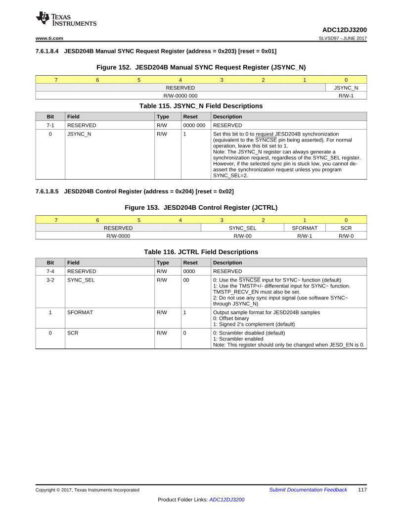
117
ADC12DJ3200www.ti.com SLVSD97 –JUNE 2017
Product Folder Links: ADC12DJ3200
Submit Documentation FeedbackCopyright © 2017, Texas Instruments Incorporated
7.6.1.8.4 JESD204B Manual SYNC Request Register (address = 0x203) [reset = 0x01]
Figure 152. JESD204B Manual SYNC Request Register (JSYNC_N)
7 6 5 4 3 2 1 0RESERVED JSYNC_N
R/W-0000 000 R/W-1
Table 115. JSYNC_N Field DescriptionsBit Field Type Reset Description7-1 RESERVED R/W 0000 000 RESERVED0 JSYNC_N R/W 1 Set this bit to 0 to request JESD204B synchronization
(equivalent to the SYNCSE pin being asserted). For normaloperation, leave this bit set to 1.Note: The JSYNC_N register can always generate asynchronization request, regardless of the SYNC_SEL register.However, if the selected sync pin is stuck low, you cannot de-assert the synchronization request unless you programSYNC_SEL=2.
7.6.1.8.5 JESD204B Control Register (address = 0x204) [reset = 0x02]
Figure 153. JESD204B Control Register (JCTRL)
7 6 5 4 3 2 1 0RESERVED SYNC_SEL SFORMAT SCRR/W-0000 R/W-00 R/W-1 R/W-0
Table 116. JCTRL Field DescriptionsBit Field Type Reset Description7-4 RESERVED R/W 0000 RESERVED3-2 SYNC_SEL R/W 00 0: Use the SYNCSE input for SYNC~ function (default)
1: Use the TMSTP+/- differential input for SYNC~ function.TMSTP_RECV_EN must also be set.2: Do not use any sync input signal (use software SYNC~through JSYNC_N)
1 SFORMAT R/W 1 Output sample format for JESD204B samples0: Offset binary1: Signed 2’s complement (default)
0 SCR R/W 0 0: Scrambler disabled (default)1: Scrambler enabledNote: This register should only be changed when JESD_EN is 0.

118
ADC12DJ3200SLVSD97 –JUNE 2017 www.ti.com
Product Folder Links: ADC12DJ3200
Submit Documentation Feedback Copyright © 2017, Texas Instruments Incorporated
7.6.1.8.6 JESD204B Test Pattern Control Register (address = 0x205) [reset = 0x00]
Figure 154. JESD204B Test Pattern Control Register (JTEST)
7 6 5 4 3 2 1 0RESERVED JTESTR/W-0000 R/W-0000
Table 117. JTEST Field DescriptionsBit Field Type Reset Description7-4 RESERVED R/W 0000 RESERVED3-0 JTEST R/W 0000 0: Test mode disabled. Normal operation (default)
1: PRBS7 test mode2: PRBS15 test mode3: PRBS23 test mode4: Ramp test mode5: Transport Layer test mode6: D21.5 test mode7: K28.5 test mode8: Repeated ILA test mode9: Modified RPAT test mode10: Serial outputs held low11: Serial outputs held high12 thru 15: RESERVEDNote: This register should only be changed when JESD_EN is 0.
7.6.1.8.7 JESD204B DID Parameter Register (address = 0x206) [reset = 0x00]
Figure 155. JESD204B DID Parameter Register (DID)
7 6 5 4 3 2 1 0DID
R/W-0000 0000
Table 118. DID Field DescriptionsBit Field Type Reset Description7-0 DID R/W 0000 0000 Specifies the DID (Device ID) value that is transmitted during the
second multiframe of the JESD204B ILA. Link A will transmitDID, and link B will transmit DID+1. Bit 0 is ignored and alwaysreturns 0 (if you program an odd number, it will be decrementedto an even number).Note: This register should only be changed when JESD_EN is 0.
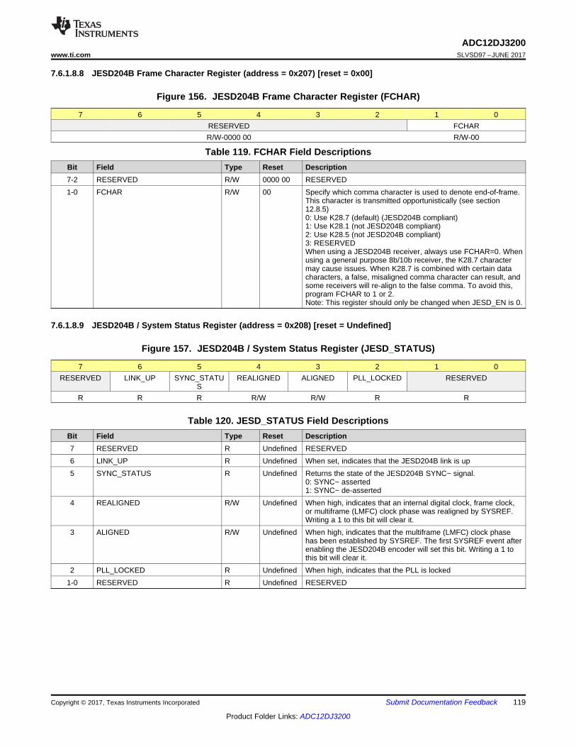
119
ADC12DJ3200www.ti.com SLVSD97 –JUNE 2017
Product Folder Links: ADC12DJ3200
Submit Documentation FeedbackCopyright © 2017, Texas Instruments Incorporated
7.6.1.8.8 JESD204B Frame Character Register (address = 0x207) [reset = 0x00]
Figure 156. JESD204B Frame Character Register (FCHAR)
7 6 5 4 3 2 1 0RESERVED FCHARR/W-0000 00 R/W-00
Table 119. FCHAR Field DescriptionsBit Field Type Reset Description7-2 RESERVED R/W 0000 00 RESERVED1-0 FCHAR R/W 00 Specify which comma character is used to denote end-of-frame.
This character is transmitted opportunistically (see section12.8.5)0: Use K28.7 (default) (JESD204B compliant)1: Use K28.1 (not JESD204B compliant)2: Use K28.5 (not JESD204B compliant)3: RESERVEDWhen using a JESD204B receiver, always use FCHAR=0. Whenusing a general purpose 8b/10b receiver, the K28.7 charactermay cause issues. When K28.7 is combined with certain datacharacters, a false, misaligned comma character can result, andsome receivers will re-align to the false comma. To avoid this,program FCHAR to 1 or 2.Note: This register should only be changed when JESD_EN is 0.
7.6.1.8.9 JESD204B / System Status Register (address = 0x208) [reset = Undefined]
Figure 157. JESD204B / System Status Register (JESD_STATUS)
7 6 5 4 3 2 1 0RESERVED LINK_UP SYNC_STATU
SREALIGNED ALIGNED PLL_LOCKED RESERVED
R R R R/W R/W R R
Table 120. JESD_STATUS Field DescriptionsBit Field Type Reset Description7 RESERVED R Undefined RESERVED6 LINK_UP R Undefined When set, indicates that the JESD204B link is up5 SYNC_STATUS R Undefined Returns the state of the JESD204B SYNC~ signal.
0: SYNC~ asserted1: SYNC~ de-asserted
4 REALIGNED R/W Undefined When high, indicates that an internal digital clock, frame clock,or multiframe (LMFC) clock phase was realigned by SYSREF.Writing a 1 to this bit will clear it.
3 ALIGNED R/W Undefined When high, indicates that the multiframe (LMFC) clock phasehas been established by SYSREF. The first SYSREF event afterenabling the JESD204B encoder will set this bit. Writing a 1 tothis bit will clear it.
2 PLL_LOCKED R Undefined When high, indicates that the PLL is locked1-0 RESERVED R Undefined RESERVED

120
ADC12DJ3200SLVSD97 –JUNE 2017 www.ti.com
Product Folder Links: ADC12DJ3200
Submit Documentation Feedback Copyright © 2017, Texas Instruments Incorporated
7.6.1.8.10 JESD204B Channel Power Down Register (address = 0x209) [reset = 0x00]
Figure 158. JESD204B Channel Power Down Register (PD_CH)
7 6 5 4 3 2 1 0RESERVED PD_BCH PD_ACHR/W-0000 00 R/W-0 R/W-0
Table 121. PD_CH Field DescriptionsBit Field Type Reset Description7-2 RESERVED R/W 0000 00 RESERVED1 PD_BCH R/W 0 When set, the “B” ADC channel is powered down. The digital
channels that are bound to the “B” ADC channel are alsopowered down (see DIG_BIND).Important notes:1. You must set JESD_EN=0 before changing PD_CH2. To power down both ADC channels, use MODE3. If both channels are powered down, then the entireJESD204B subsystem (including the PLL and LMFC) arepowered down4. If the selected JESD204B mode transmits A and B data onlink A, and the B digital channel is disabled, link A remainsoperational, but the B-channel samples are undefined.
0 PD_ACH R/W 0 When set, the “A” ADC channel is powered down. The digitalchannels that are bound to the “A” ADC channel are alsopowered down (see DIG_BIND).Important notes:1. You must set JESD_EN=0 before changing PD_CH2. To power down both ADC channels, use MODE3. If both channels are powered down, then the entireJESD204B subsystem (including the PLL and LMFC) arepowered down4. If the selected JESD204B mode transmits A and B data onlink A, and the B digital channel is disabled, link A remainsoperational, but the B-channel samples are undefined.

121
ADC12DJ3200www.ti.com SLVSD97 –JUNE 2017
Product Folder Links: ADC12DJ3200
Submit Documentation FeedbackCopyright © 2017, Texas Instruments Incorporated
7.6.1.8.11 JESD204B Extra Lane Enable (Link A) Register (address = 0x20A) [reset = 0x00]
Figure 159. JESD204B Extra Lane Enable (Link A) Register (JEXTRA_A)
7 6 5 4 3 2 1 0EXTRA_LANE_A EXTRA_SER_
AR/W-0000 000 R/W-0
Table 122. JESD204B Extra Lane Enable (Link A) Field DescriptionsBit Field Type Reset Description7-1 EXTRA_LANE_A R/W 0000 000 Program these register bits to enable extra lanes (even if the
selected JMODE does not require the lanes to be enabled).EXTRA_LANE_A(n) enables An (n=1 to 7). This register enablesthe link layer clocks for the affected lanes. To also enable theextra serializes set EXTRA_SER_A=1.
0 EXTRA_SER_A R/W 0 0: Only the link layer clocks for extra lanes are enabled.1: Serializers for extra lanes are also enabled. Use this mode totransmit data from the extra lanes.Important notes:This register should only be changed when JESD_EN=0.The bit-rate and mode of the extra lanes are set by the JMODEand JTEST parameters.This register does not override the PD_CH register, so ensurethat the link is enabled to use this feature.To enable serializer 'n', the lower number lanes 0 to n-1 mustalso be enabled, otherwise serializer 'n' will not receive a clock.
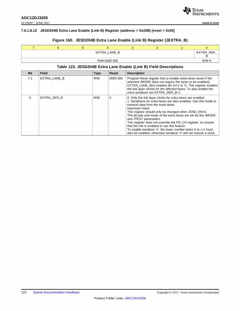
122
ADC12DJ3200SLVSD97 –JUNE 2017 www.ti.com
Product Folder Links: ADC12DJ3200
Submit Documentation Feedback Copyright © 2017, Texas Instruments Incorporated
7.6.1.8.12 JESD204B Extra Lane Enable (Link B) Register (address = 0x20B) [reset = 0x00]
Figure 160. JESD204B Extra Lane Enable (Link B) Register (JEXTRA_B)
7 6 5 4 3 2 1 0EXTRA_LANE_B EXTRA_SER_
BR/W-0000 000 R/W-0
Table 123. JESD204B Extra Lane Enable (Link B) Field DescriptionsBit Field Type Reset Description7-1 EXTRA_LANE_B R/W 0000 000 Program these register bits to enable extra lanes (even if the
selected JMODE does not require the lanes to be enabled).EXTRA_LANE_B(n) enables Bn (n=1 to 7). This register enablesthe link layer clocks for the affected lanes. To also enable theextra serializes set EXTRA_SER_B=1.
0 EXTRA_SER_B R/W 0 0: Only the link layer clocks for extra lanes are enabled.1: Serializers for extra lanes are also enabled. Use this mode totransmit data from the extra lanes.Important notes:This register should only be changed when JESD_EN=0.The bit-rate and mode of the extra lanes are set by the JMODEand JTEST parameters.This register does not override the PD_CH register, so ensurethat the link is enabled to use this feature.To enable serializer 'n', the lower number lanes 0 to n-1 mustalso be enabled, otherwise serializer 'n' will not receive a clock.
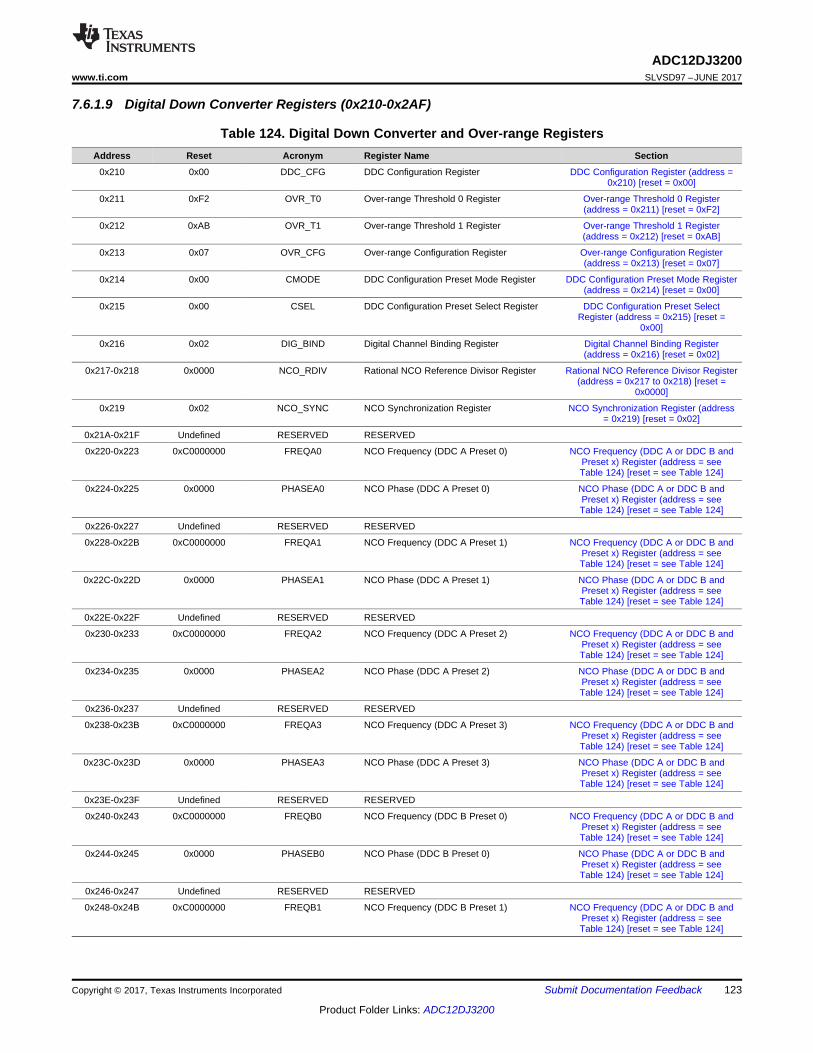
123
ADC12DJ3200www.ti.com SLVSD97 –JUNE 2017
Product Folder Links: ADC12DJ3200
Submit Documentation FeedbackCopyright © 2017, Texas Instruments Incorporated
7.6.1.9 Digital Down Converter Registers (0x210-0x2AF)
Table 124. Digital Down Converter and Over-range RegistersAddress Reset Acronym Register Name Section
0x210 0x00 DDC_CFG DDC Configuration Register DDC Configuration Register (address =0x210) [reset = 0x00]
0x211 0xF2 OVR_T0 Over-range Threshold 0 Register Over-range Threshold 0 Register(address = 0x211) [reset = 0xF2]
0x212 0xAB OVR_T1 Over-range Threshold 1 Register Over-range Threshold 1 Register(address = 0x212) [reset = 0xAB]
0x213 0x07 OVR_CFG Over-range Configuration Register Over-range Configuration Register(address = 0x213) [reset = 0x07]
0x214 0x00 CMODE DDC Configuration Preset Mode Register DDC Configuration Preset Mode Register(address = 0x214) [reset = 0x00]
0x215 0x00 CSEL DDC Configuration Preset Select Register DDC Configuration Preset SelectRegister (address = 0x215) [reset =
0x00]
0x216 0x02 DIG_BIND Digital Channel Binding Register Digital Channel Binding Register(address = 0x216) [reset = 0x02]
0x217-0x218 0x0000 NCO_RDIV Rational NCO Reference Divisor Register Rational NCO Reference Divisor Register(address = 0x217 to 0x218) [reset =
0x0000]
0x219 0x02 NCO_SYNC NCO Synchronization Register NCO Synchronization Register (address= 0x219) [reset = 0x02]
0x21A-0x21F Undefined RESERVED RESERVED
0x220-0x223 0xC0000000 FREQA0 NCO Frequency (DDC A Preset 0) NCO Frequency (DDC A or DDC B andPreset x) Register (address = seeTable 124) [reset = see Table 124]
0x224-0x225 0x0000 PHASEA0 NCO Phase (DDC A Preset 0) NCO Phase (DDC A or DDC B andPreset x) Register (address = seeTable 124) [reset = see Table 124]
0x226-0x227 Undefined RESERVED RESERVED
0x228-0x22B 0xC0000000 FREQA1 NCO Frequency (DDC A Preset 1) NCO Frequency (DDC A or DDC B andPreset x) Register (address = seeTable 124) [reset = see Table 124]
0x22C-0x22D 0x0000 PHASEA1 NCO Phase (DDC A Preset 1) NCO Phase (DDC A or DDC B andPreset x) Register (address = seeTable 124) [reset = see Table 124]
0x22E-0x22F Undefined RESERVED RESERVED
0x230-0x233 0xC0000000 FREQA2 NCO Frequency (DDC A Preset 2) NCO Frequency (DDC A or DDC B andPreset x) Register (address = seeTable 124) [reset = see Table 124]
0x234-0x235 0x0000 PHASEA2 NCO Phase (DDC A Preset 2) NCO Phase (DDC A or DDC B andPreset x) Register (address = seeTable 124) [reset = see Table 124]
0x236-0x237 Undefined RESERVED RESERVED
0x238-0x23B 0xC0000000 FREQA3 NCO Frequency (DDC A Preset 3) NCO Frequency (DDC A or DDC B andPreset x) Register (address = seeTable 124) [reset = see Table 124]
0x23C-0x23D 0x0000 PHASEA3 NCO Phase (DDC A Preset 3) NCO Phase (DDC A or DDC B andPreset x) Register (address = seeTable 124) [reset = see Table 124]
0x23E-0x23F Undefined RESERVED RESERVED
0x240-0x243 0xC0000000 FREQB0 NCO Frequency (DDC B Preset 0) NCO Frequency (DDC A or DDC B andPreset x) Register (address = seeTable 124) [reset = see Table 124]
0x244-0x245 0x0000 PHASEB0 NCO Phase (DDC B Preset 0) NCO Phase (DDC A or DDC B andPreset x) Register (address = seeTable 124) [reset = see Table 124]
0x246-0x247 Undefined RESERVED RESERVED
0x248-0x24B 0xC0000000 FREQB1 NCO Frequency (DDC B Preset 1) NCO Frequency (DDC A or DDC B andPreset x) Register (address = seeTable 124) [reset = see Table 124]

124
ADC12DJ3200SLVSD97 –JUNE 2017 www.ti.com
Product Folder Links: ADC12DJ3200
Submit Documentation Feedback Copyright © 2017, Texas Instruments Incorporated
Table 124. Digital Down Converter and Over-range Registers (continued)Address Reset Acronym Register Name Section
0x24C-0x24D 0x0000 PHASEB1 NCO Phase (DDC B Preset 1) NCO Phase (DDC A or DDC B andPreset x) Register (address = seeTable 124) [reset = see Table 124]
0x24E-0x24F Undefined RESERVED RESERVED
0x250-0x253 0xC0000000 FREQB2 NCO Frequency (DDC B Preset 2) NCO Frequency (DDC A or DDC B andPreset x) Register (address = seeTable 124) [reset = see Table 124]
0x254-0x255 0x0000 PHASEB2 NCO Phase (DDC B Preset 2) NCO Phase (DDC A or DDC B andPreset x) Register (address = seeTable 124) [reset = see Table 124]
0x256-0x257 Undefined RESERVED RESERVED
0x258-0x25B 0xC0000000 FREQB3 NCO Frequency (DDC B Preset 3) NCO Frequency (DDC A or DDC B andPreset x) Register (address = seeTable 124) [reset = see Table 124]
0x25C-0x25D 0x0000 PHASEB3 NCO Phase (DDC B Preset 3) NCO Phase (DDC A or DDC B andPreset x) Register (address = seeTable 124) [reset = see Table 124]
0x25E-0x296 Undefined RESERVED RESERVED
0x297 Undefined SPIN_ID Spin Identification Value Spin Identification Register (address =0x297) [reset = Undefined]
0x298-0x2AF Undefined RESERVED RESERVED

125
ADC12DJ3200www.ti.com SLVSD97 –JUNE 2017
Product Folder Links: ADC12DJ3200
Submit Documentation FeedbackCopyright © 2017, Texas Instruments Incorporated
7.6.1.9.1 DDC Configuration Register (address = 0x210) [reset = 0x00]
Figure 161. DDC Configuration Register (DDC_CFG)
7 6 5 4 3 2 1 0RESERVED D4_AP87 D2_HIGH_PAS
SINVERT_SPEC
TRUMBOOST
R/W-0000 R/W-0 R/W-0 R/W-0 R/W-0
Table 125. DDC_CFG Field DescriptionsBit Field Type Reset Description7-4 RESERVED R/W 0000 RESERVED3 D4_AP87 R/W 0 0: Decimate-by-4 mode uses 80% alias protection, >80dB
suppression1: Decimate-by-4 mode uses 87.5% alias protection, >60dBsuppression
2 D2_HIGH_PASS R/W 0 0: Decimate-by-2 mode uses a low-pass filter1: Decimate-by-2 mode uses a high-pass filter. Decimating thehigh-pass signal will cause spectral inversion. This can beundone by setting INVERT_SPECTRUM.
1 INVERT_SPECTRUM R/W 0 0: No inversion applied to output spectrum1: Output spectrum is invertedThis register only applies when the DDC is enabled and isproducing a real output (not complex). The spectrum is invertedby mixing the signal with FSOUT/2 (i.e. invert all odd samples).
0 BOOST R/W 0 DDC gain control. Only applies to DDC modes with complexdecimation.0: Final filter has 0dB gain (default)1: Final filter has 6.02dB gain. Only use this when you arecertain the negative image of your input signal is filtered out bythe DDC, otherwise digital clipping may occur.
7.6.1.9.2 Over-range Threshold 0 Register (address = 0x211) [reset = 0xF2]
Figure 162. Over-range Threshold 0 Register (OVR_T0)
7 6 5 4 3 2 1 0OVR_T0
R/W-1111 0010
Table 126. OVR_T0 Field DescriptionsBit Field Type Reset Description7-0 OVR_T0 R/W 1111 0010 Over-range threshold 0. This parameter defines the absolute
sample level that causes control bit 0 to be set. The detectionlevel in dBFS (peak) is20log10(OVR_T0 / 256)Default: 0xF2 = 242 → –0.5 dBFS

126
ADC12DJ3200SLVSD97 –JUNE 2017 www.ti.com
Product Folder Links: ADC12DJ3200
Submit Documentation Feedback Copyright © 2017, Texas Instruments Incorporated
7.6.1.9.3 Over-range Threshold 1 Register (address = 0x212) [reset = 0xAB]
Figure 163. Over-range Threshold 1 Register (OVR_T1)
7 6 5 4 3 2 1 0OVR_T1
R/W-1010 1011
Table 127. OVR_T1 Field DescriptionsBit Field Type Reset Description7-0 OVR_T1 R/W 1010 1011 Over-range threshold 1. This parameter defines the absolute
sample level that causes control bit 1 to be set. The detectionlevel in dBFS (peak) is20log10(OVR_T1 / 256)Default: 0xAB = 171 → –3.5 dBFS
7.6.1.9.4 Over-range Configuration Register (address = 0x213) [reset = 0x07]
Figure 164. Over-range Configuration Register (OVR_CFG)
7 6 5 4 3 2 1 0RESERVED OVR_EN OVR_NR/W-0000 R/W-0 R/W-111
(1) Changing the OVR_N setting while JESD_EN=1 may cause the phase of the monitoring period to change.
Table 128. OVR_CFG Field DescriptionsBit Field Type Reset Description7-4 RESERVED R/W 0000 0 RESERVED3 OVR_EN R/W 0 Enables over-range status output pins when set high. The
ORA0, ORA1, ORB0 and ORB1 outputs are held low whenOVR_EN is set low. This register only effects the over-rangeoutput pins (ORxx) and not the over-range status embedded inthe data samples.
2-0 OVR_N (1) R/W 111 Program this register to adjust the pulse extension for theORA0/1 and ORB0/1 outputs. The minimum pulse duration ofthe over-range outputs is 8 * 2OVR_N DEVCLK cycles.Incrementing this field doubles the monitoring period.

127
ADC12DJ3200www.ti.com SLVSD97 –JUNE 2017
Product Folder Links: ADC12DJ3200
Submit Documentation FeedbackCopyright © 2017, Texas Instruments Incorporated
7.6.1.9.5 DDC Configuration Preset Mode Register (address = 0x214) [reset = 0x00]
Figure 165. DDC Configuration Preset Mode Register (CMODE)
7 6 5 4 3 2 1 0RESERVED CMODER/W-0000 00 R/W-00
Table 129. CMODE Field DescriptionsBit Field Type Reset Description7-2 RESERVED R/W 0000 00 RESERVED1-0 CMODE R/W 00 The NCO frequency and phase for DDC A are set by the
FREQAx and PHASEAx registers and the NCO frequency andphase for DDC B are set by the FREQBx and PHASEBxregisters, where x is the configuration preset (0 through 3).0: Use CSEL register to select the active NCO configurationpreset for DDC A and DDC B1: Use NCOA[1:0] pins to select the active NCO configurationpreset for DDC A and use NCOB[1:0] pins to select the activeNCO configuration preset for DDC B2: Use NCOA[1:0] pins to select the active NCO configurationpreset for both DDC A and DDC B3: RESERVED

128
ADC12DJ3200SLVSD97 –JUNE 2017 www.ti.com
Product Folder Links: ADC12DJ3200
Submit Documentation Feedback Copyright © 2017, Texas Instruments Incorporated
7.6.1.9.6 DDC Configuration Preset Select Register (address = 0x215) [reset = 0x00]
Figure 166. DDC Configuration Preset Select Register (CSEL)
7 6 5 4 3 2 1 0RESERVED CSELB CSELAR/W-0000 R/W-00 R/W-00
Table 130. CSEL Field DescriptionsBit Field Type Reset Description7-4 RESERVED R/W 0000 RESERVED3-2 CSELB R/W 00 When CMODE=0, this register is used to select the active NCO
configuration preset for DDC B1-0 CSELA R/W 00 When CMODE=0, this register is used to select the active NCO
configuration preset for DDC AExample: If CSELA=0, then FREQA0 and PHASEA0 are theactive settings. If CSELA=1, then FREQA1 and PHASEA1 arethe active settings.
7.6.1.9.7 Digital Channel Binding Register (address = 0x216) [reset = 0x02]
Figure 167. Digital Channel Binding Register (DIG_BIND)
7 6 5 4 3 2 1 0RESERVED DIG_BIND_B DIG_BIND_AR/W-0000 00 R/W-1 R/W-0
Table 131. DIG_BIND Field DescriptionsBit Field Type Reset Description7-2 RESERVED R/W 0000 00 RESERVED1 DIG_BIND_B R/W 0 Digital channel B input select:
0: Digital channel B receives data from ADC channel A1: Digital channel B receives data from ADC channel B (default)
0 DIG_BIND_A R/W 0 Digital channel A input select:0: Digital channel A receives data from ADC channel A (default)1: Digital channel A receives data from ADC channel BNote 1: When using single channel mode, you must always usethe default setting for DIG_BIND or the part will not work.Note 2: You must set JESD_EN=0 and CAL_EN=0 beforechanging DIG_BIND.Note 3: The DIG_BIND setting is combined withPD_ACH/PD_BCH to determine if a digital channel is powereddown. Each digital channel (and link) is powered down when theADC channel it is bound to is powered down (byPD_ACH/PD_BCH).

129
ADC12DJ3200www.ti.com SLVSD97 –JUNE 2017
Product Folder Links: ADC12DJ3200
Submit Documentation FeedbackCopyright © 2017, Texas Instruments Incorporated
7.6.1.9.8 Rational NCO Reference Divisor Register (address = 0x217 to 0x218) [reset = 0x0000]
Figure 168. Rational NCO Reference Divisor Register (NCO_RDIV)
15 14 13 12 11 10 9 8NCO_RDIV[15:8]R/W-0000 0000
7 6 5 4 3 2 1 0NCO_RDIV[7:0]R/W-0000 0000
Table 132. NCO_RDIV Field DescriptionsBit Field Type Reset Description
15-0 NCO_RDIV R/W 0x0000h Sometimes the 32-bit NCO frequency word does not provide thedesired frequency step size and can only approximate thedesired frequency. This results in a frequency error. Use thisregister to eliminate the frequency error. This register is used forall configuration presets. See .
7.6.1.9.9 NCO Synchronization Register (address = 0x219) [reset = 0x02]
Figure 169. NCO Synchronization Register (NCO_SYNC)
7 6 5 4 3 2 1 0RESERVED NCO_SYNC_IL
ANCO_SYNC_N
EXTR/W-0000 00 R/W-1 R/W-0
Table 133. NCO_SYNC Field DescriptionsBit Field Type Reset Description7-2 RESERVED R/W 0000 00 RESERVED1 NCO_SYNC_ILA R/W 0 When this bit is set, the NCO phase is initialized by the LMFC
edge that starts the ILA sequence (default)0 NCO_SYNC_NEXT R/W 0 After writing ‘0’ and then ‘1’ to this bit, the next SYSREF rising
edge will initialize the NCO phase. Once the NCO phase hasbeen initialized by SYSREF, the NCO will not re-initialize onfuture SYSREF edges unless ‘0’ and ‘1’ is written to this bitagain.Use this to align the NCO in multiple parts:• Ensure the part is powered up, JESD_EN is set, and the
device clock is running.• Ensure that SYSREF is disabled (not toggling).• Program NCO_SYNC_ILA=0 on all parts.• Write NCO_SYNC_NEXT=0 on all parts.• Write NCO_SYNC_NEXT=1 on all parts. NCO sync is
armed.• Instruct the SYSREF source to generate 1 or more SYSREF
pulses.• All parts will initialize their NCO using the first SYSREF
rising edge.

130
ADC12DJ3200SLVSD97 –JUNE 2017 www.ti.com
Product Folder Links: ADC12DJ3200
Submit Documentation Feedback Copyright © 2017, Texas Instruments Incorporated
7.6.1.9.10 NCO Frequency (DDC A or DDC B and Preset x) Register (address = see Table 124) [reset = seeTable 124]
Figure 170. NCO Frequency (DDC A or DDC B and Preset x) Register (FREQAx or FREQBx)
31 30 29 28 27 26 25 24FREQAx[31:24] or FREQBx[31:24]
R/W-0xC0
23 22 21 20 19 18 17 16FREQAx[23:16] or FREQBx[23:16]
R/W-0x00
15 14 13 12 11 10 9 8FREQAx[15:8] or FREQBx[15:8]
R/W-0x00
7 6 5 4 3 2 1 0FREQAx[7:0] or FREQBx[7:0]
R/W-0x00
Table 134. FREQAx or FREQBx Field DescriptionsBit Field Type Reset Description
31-0 FREQAx or FREQBx R/W SeeTable 124
Changing this register after the JESD204B interface is runningresults in non-deterministic NCO phase. If deterministic phase isrequired, the JESD204B interface must be re-initialized afterchanging this register. This register can be interpreted as signedor unsigned. See .
7.6.1.9.11 NCO Phase (DDC A or DDC B and Preset x) Register (address = see Table 124) [reset = see Table 124]
Figure 171. NCO Phase (DDC A or DDC B and Preset x) Register (PHASEAx or PHASEBx)
15 14 13 12 11 10 9 8PHASEAx[15:8] or PHASEBx[15:8]
R/W-0x00
7 6 5 4 3 2 1 0PHASEAx[7:0] or PHASEBx[7:0]
R/W-0x00
Table 135. PHASEAx or PHASEBx Field DescriptionsBit Field Type Reset Description
15-0 PHASEAx or PHASEBx R/W SeeTable 124
This value is MSB-justified into a 32−bit field and then added tothe phase accumulator. This register can be interpreted assigned or unsigned. See NCO Phase Offset Setting.

131
ADC12DJ3200www.ti.com SLVSD97 –JUNE 2017
Product Folder Links: ADC12DJ3200
Submit Documentation FeedbackCopyright © 2017, Texas Instruments Incorporated
7.6.1.10 Spin Identification Register (address = 0x297) [reset = Undefined]
Figure 172. Spin Identification Register (SPIN_ID)
7 6 5 4 3 2 1 0RESERVED SPIN_ID
R-000 R
Table 136. SPIN_ID Field DescriptionsBit Field Type Reset Description7-5 RESERVED R 000 RESERVED4-0 SPIN_ID R See
descriptionSpin identification value:0 : ADC12DJ3200
7.6.2 SYSREF Calibration Registers (0x2B0 to 0x2BF)
Table 137. SYSREF Calibration RegistersAddress Reset Acronym Register Name Section
0x2B0 0x00 SRC_EN SYSREF Calibration Enable Register SYSREF Calibration Enable Register(address = 0x2B0) [reset = 0x00]
0x2B1 0x05 SRC_CFG SYSREF Calibration Configuration Register SYSREF Calibration ConfigurationRegister (address = 0x2B1) [reset =
0x05]
0x2B2-0x2B4 Undefined SRC_STATUS SYSREF Calibration Status SYSREF Calibration Status Register(address = 0x2B2 to 0x2B4) [reset =
Undefined]
0x2B5-0x2B7 0x00 TAD DEVCLK Aperture Delay Adjustment Register DEVCLK Aperture Delay AdjustmentRegister (address = 0x2B5 to 0x2B7)
[reset = 0x000000]
0x2B8 0x00 TAD_RAMP DEVCLK Timing Adjust Ramp ControlRegister
DEVCLK Timing Adjust Ramp ControlRegister (address = 0x2B8) [reset =
0x00]
0x2B9-0x2BF Undefined RESERVED RESERVED
7.6.2.1 SYSREF Calibration Enable Register (address = 0x2B0) [reset = 0x00]
Figure 173. SYSREF Calibration Enable Register (SRC_EN)
7 6 5 4 3 2 1 0RESERVED SRC_EN
R/W-0000 000 R/W-0
Table 138. SRC_EN Field DescriptionsBit Field Type Reset Description7-1 RESERVED R/W 0000 000 RESERVED0 SRC_EN R/W 0 0: SYSREF Calibration Disabled. Use the TAD register to
manually control the tad[16:0] output and adjust the DEVCLKdelay. (default)1: SYSREF Calibration Enabled. The DEVCLK delay isautomatically calibrated. The TAD register is ignored.A 0-to-1 transition on SRC_EN starts the SYSREF calibrationsequence. Program SRC_CFG before setting SRC_EN. Ensurethat ADC calibration is not currently running before settingSRC_EN.

132
ADC12DJ3200SLVSD97 –JUNE 2017 www.ti.com
Product Folder Links: ADC12DJ3200
Submit Documentation Feedback Copyright © 2017, Texas Instruments Incorporated
7.6.2.2 SYSREF Calibration Configuration Register (address = 0x2B1) [reset = 0x05]
Figure 174. SYSREF Calibration Configuration Register (SRC_CFG)
7 6 5 4 3 2 1 0RESERVED SRC_AVG SRC_HDURR/W-0000 R/W-01 R/W-01
Table 139. SRC_CFG Field DescriptionsBit Field Type Reset Description7-4 RESERVED R/W 0000 00 RESERVED3-2 SRC_AVG R/W 01 Specifies the amount of averaging used for SYSREF Calibration.
Larger values will increase calibration time and reduce thevariance of the calibrated value.0: 4 averages1: 16 averages2: 64 averages3: 256 averages
1-0 SRC_HDUR R/W 01 Specifies the duration of each high-speed accumulation forSYSREF Calibration. If the SYSREF period exceeds thesupported value, calibration will fail. Larger values will increasecalibration time and support longer SYSREF periods. For agiven SYSREF period, larger values will also reduce thevariance of the calibrated value.0: 4 cycles per accumulation, max SYSREF period of 85DEVCLK cycles1: 16 cycles per accumulation, max SYSREF period of 1100DEVCLK cycles2: 64 cycles per accumulation, max SYSREF period of 5200DEVCLK cycles3: 256 cycles per accumulation, max SYSREF period of 21580DEVCLK cyclesMax duration of SYSREF calibration is bounded by:TSYSREFCAL (in DEVCLK cycles) = 256 * 19 * 4(SRC_AVG +SRC_HDUR + 2)
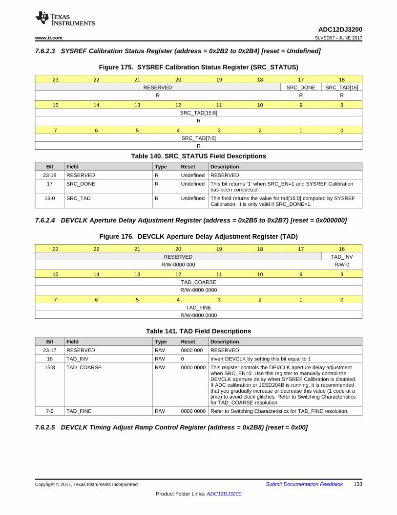
133
ADC12DJ3200www.ti.com SLVSD97 –JUNE 2017
Product Folder Links: ADC12DJ3200
Submit Documentation FeedbackCopyright © 2017, Texas Instruments Incorporated
7.6.2.3 SYSREF Calibration Status Register (address = 0x2B2 to 0x2B4) [reset = Undefined]
Figure 175. SYSREF Calibration Status Register (SRC_STATUS)
23 22 21 20 19 18 17 16RESERVED SRC_DONE SRC_TAD[16]
R R R
15 14 13 12 11 10 9 8SRC_TAD[15:8]
R
7 6 5 4 3 2 1 0SRC_TAD[7:0]
R
Table 140. SRC_STATUS Field DescriptionsBit Field Type Reset Description
23-18 RESERVED R Undefined RESERVED17 SRC_DONE R Undefined This bit returns ‘1’ when SRC_EN=1 and SYSREF Calibration
has been completed16-0 SRC_TAD R Undefined This field returns the value for tad[16:0] computed by SYSREF
Calibration. It is only valid if SRC_DONE=1.
7.6.2.4 DEVCLK Aperture Delay Adjustment Register (address = 0x2B5 to 0x2B7) [reset = 0x000000]
Figure 176. DEVCLK Aperture Delay Adjustment Register (TAD)
23 22 21 20 19 18 17 16RESERVED TAD_INV
R/W-0000 000 R/W-0
15 14 13 12 11 10 9 8TAD_COARSER/W-0000 0000
7 6 5 4 3 2 1 0TAD_FINE
R/W-0000 0000
Table 141. TAD Field DescriptionsBit Field Type Reset Description
23-17 RESERVED R/W 0000 000 RESERVED16 TAD_INV R/W 0 Invert DEVCLK by setting this bit equal to 1
15-8 TAD_COARSE R/W 0000 0000 This register controls the DEVCLK aperture delay adjustmentwhen SRC_EN=0. Use this register to manually control theDEVCLK aperture delay when SYSREF Calibration is disabled.If ADC calibration or JESD204B is running, it is recommendedthat you gradually increase or decrease this value (1 code at atime) to avoid clock glitches. Refer to Switching Characteristicsfor TAD_COARSE resolution.
7-0 TAD_FINE R/W 0000 0000 Refer to Switching Characteristics for TAD_FINE resolution.
7.6.2.5 DEVCLK Timing Adjust Ramp Control Register (address = 0x2B8) [reset = 0x00]
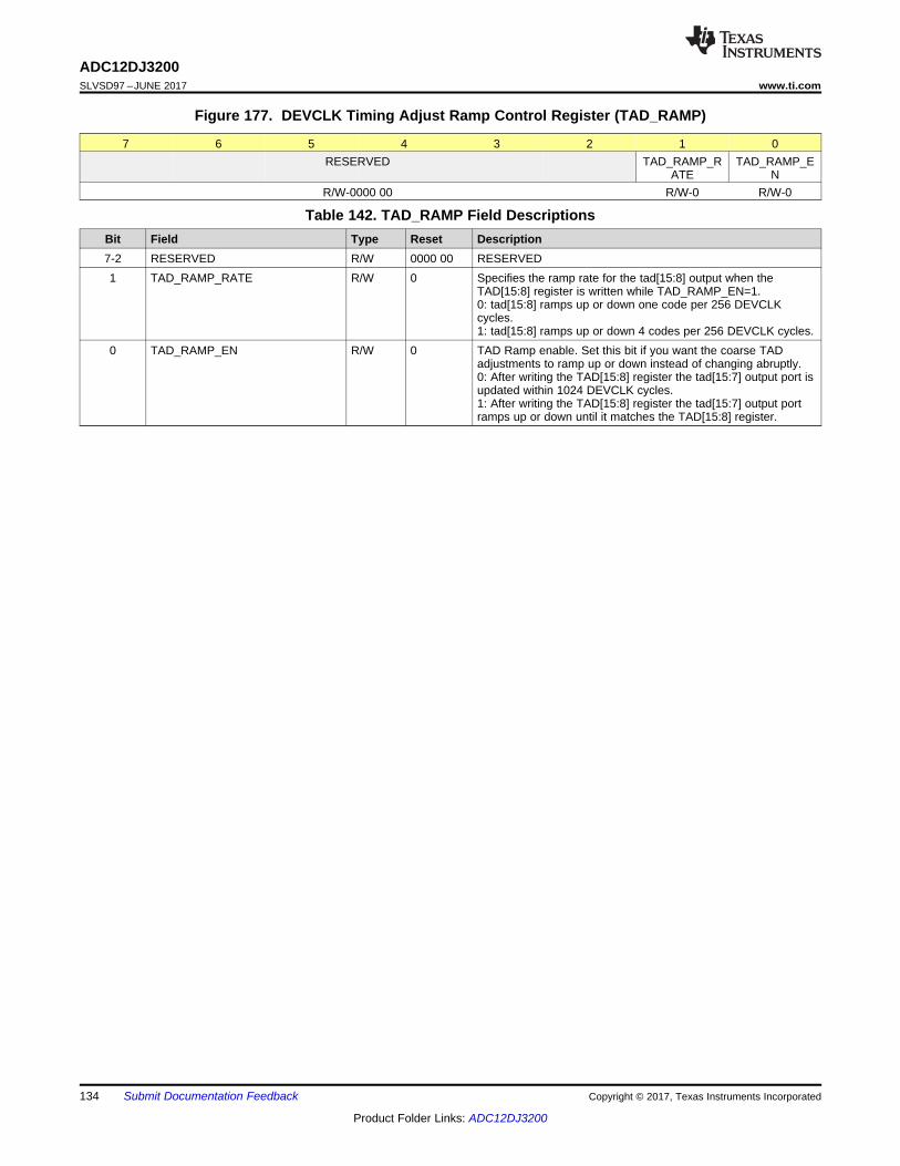
134
ADC12DJ3200SLVSD97 –JUNE 2017 www.ti.com
Product Folder Links: ADC12DJ3200
Submit Documentation Feedback Copyright © 2017, Texas Instruments Incorporated
Figure 177. DEVCLK Timing Adjust Ramp Control Register (TAD_RAMP)
7 6 5 4 3 2 1 0RESERVED TAD_RAMP_R
ATETAD_RAMP_E
NR/W-0000 00 R/W-0 R/W-0
Table 142. TAD_RAMP Field DescriptionsBit Field Type Reset Description7-2 RESERVED R/W 0000 00 RESERVED1 TAD_RAMP_RATE R/W 0 Specifies the ramp rate for the tad[15:8] output when the
TAD[15:8] register is written while TAD_RAMP_EN=1.0: tad[15:8] ramps up or down one code per 256 DEVCLKcycles.1: tad[15:8] ramps up or down 4 codes per 256 DEVCLK cycles.
0 TAD_RAMP_EN R/W 0 TAD Ramp enable. Set this bit if you want the coarse TADadjustments to ramp up or down instead of changing abruptly.0: After writing the TAD[15:8] register the tad[15:7] output port isupdated within 1024 DEVCLK cycles.1: After writing the TAD[15:8] register the tad[15:7] output portramps up or down until it matches the TAD[15:8] register.

135
ADC12DJ3200www.ti.com SLVSD97 –JUNE 2017
Product Folder Links: ADC12DJ3200
Submit Documentation FeedbackCopyright © 2017, Texas Instruments Incorporated
7.6.3 Alarm Registers (0x2C0 to 0x2C2)
Table 143. Alarm RegistersAddress Reset Acronym Register Name Section
0x2C0 Undefined ALARM Alarm Interrupt Status Register Alarm Interrupt Register (address =0x2C0) [reset = Undefined]
0x2C1 0x1F ALM_STATUS Alarm Status Register Alarm Status Register (address = 0x2C1)[reset = 0x1F]
0x2C2 0x1F ALM_MASK Alarm Mask Register Alarm Mask Register (address = 0x2C2)[reset = 0x1F]
7.6.3.1 Alarm Interrupt Register (address = 0x2C0) [reset = Undefined]
Figure 178. Alarm Interrupt Register (ALARM)
7 6 5 4 3 2 1 0RESERVED ALARM
R R
Table 144. ALARM Field DescriptionsBit Field Type Reset Description7-1 RESERVED R Undefined RESERVED0 ALARM R Undefined This bit returns a ‘1’ whenever any alarm occurs that is
unmasked in the ALM_STATUS register. Use ALM_MASK tomask (disable) individual alarms. CAL_STATUS_SEL can beused to drive the ALARM bit onto the CALSTAT output pin toprovide a hardware alarm interrupt signal.
7.6.3.2 Alarm Status Register (address = 0x2C1) [reset = 0x1F]
Figure 179. Alarm Status Register (ALM_STATUS)
7 6 5 4 3 2 1 0RESERVED PLL_ALM LINK_ALM REALIGNED_A
LMNCO_ALM CLK_ALM
R/W-000 R/W-1 R/W-1 R/W-1 R/W-1 R/W-1
Table 145. ALM_STATUS Field DescriptionsBit Field Type Reset Description7-5 RESERVED R/W 000 RESERVED4 PLL_ALM R/W 1 PLL Lock Lost Alarm: This bit is set whenever the PLL is not
locked. Write a ‘1’ to clear this bit.3 LINK_ALM R/W 1 Link Alarm: This bit is set whenever the JESD204B link is
enabled, but is not in the DATA_ENC state. Write a ‘1’ to clearthis bit.
2 REALIGNED_ALM R/W 1 Realigned Alarm: This bit is set whenever SYSREF causes theinternal clocks (including the LMFC) to be realigned. Write a ‘1’to clear this bit.
1 NCO_ALM R/W 1 NCO Alarm: This bit can be used to detect an upset to the NCOphase. This bit is set when any of the following occur:• The NCOs are disabled (JESD_EN=0)• The NCOs are synchronized (intentionally or unintentionally)• Any phase accumulators in channel A do not match channel
BWrite a ‘1’ to clear this bit.
0 CLK_ALM R/W 1 Clock Alarm: This bit can be used to detect an upset to thedigital block and JESD204B clocks. This bit is set whenever theinternal clock dividers for the A and B channels do not match.Write a ‘1’ to clear this bit.
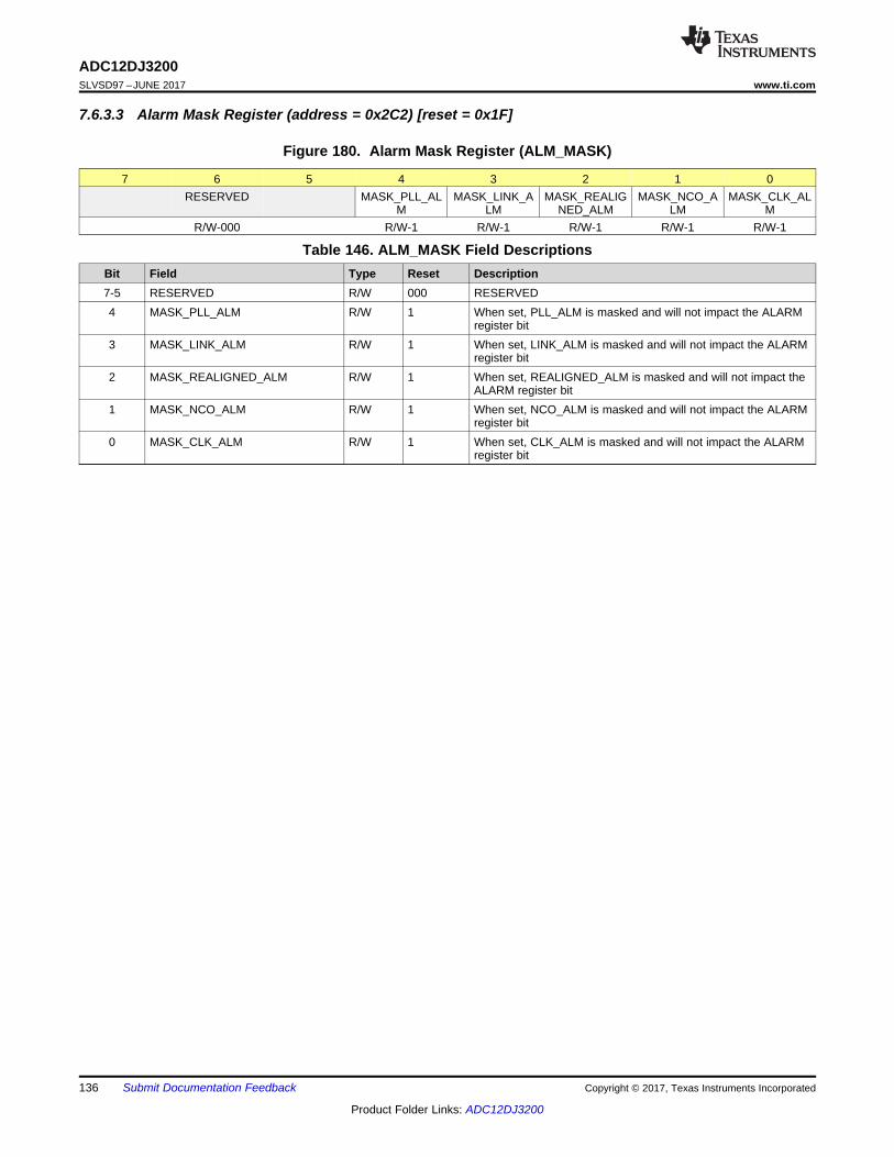
136
ADC12DJ3200SLVSD97 –JUNE 2017 www.ti.com
Product Folder Links: ADC12DJ3200
Submit Documentation Feedback Copyright © 2017, Texas Instruments Incorporated
7.6.3.3 Alarm Mask Register (address = 0x2C2) [reset = 0x1F]
Figure 180. Alarm Mask Register (ALM_MASK)
7 6 5 4 3 2 1 0RESERVED MASK_PLL_AL
MMASK_LINK_A
LMMASK_REALIG
NED_ALMMASK_NCO_A
LMMASK_CLK_AL
MR/W-000 R/W-1 R/W-1 R/W-1 R/W-1 R/W-1
Table 146. ALM_MASK Field DescriptionsBit Field Type Reset Description7-5 RESERVED R/W 000 RESERVED4 MASK_PLL_ALM R/W 1 When set, PLL_ALM is masked and will not impact the ALARM
register bit3 MASK_LINK_ALM R/W 1 When set, LINK_ALM is masked and will not impact the ALARM
register bit2 MASK_REALIGNED_ALM R/W 1 When set, REALIGNED_ALM is masked and will not impact the
ALARM register bit1 MASK_NCO_ALM R/W 1 When set, NCO_ALM is masked and will not impact the ALARM
register bit0 MASK_CLK_ALM R/W 1 When set, CLK_ALM is masked and will not impact the ALARM
register bit

ADC
ADC
ADC and
JESD204B
Clocking
User Control
Logic
SPI
DEVICE CLK
SYSREF
SYNC~
VINA
VINB
FPGA
1 to 16 lanes
JESD204B
JESD
204BDDC
DDCJESD
204B
1:2 Balun
Transformers
137
ADC12DJ3200www.ti.com SLVSD97 –JUNE 2017
Product Folder Links: ADC12DJ3200
Submit Documentation FeedbackCopyright © 2017, Texas Instruments Incorporated
(1) See Third-party Products Disclaimer
8 Application and Implementation
NOTEInformation in the following applications sections is not part of the TI componentspecification, and TI does not warrant its accuracy or completeness. TI’s customers areresponsible for determining suitability of components for their purposes. Customers shouldvalidate and test their design implementation to confirm system functionality.
8.1 Application Information
8.2 Typical Application
Figure 181. Typical Configuration for Wideband RF Sampling
8.2.1 Design Requirements
8.2.1.1 Input Signal PathAppropriate band limiting filters should be utilized to reject unwanted frequencies in the input signal path.
A 1:2 balun transformer is needed to convert the 50-Ω single-ended signal to 100-Ω differential for input to theADC. The balun outputs can be either AC-coupled, or directly connected to the ADC differential inputs, which areterminated internally to GND.
Drivers should be selected to provide any needed signal gain, and which have the necessary bandwidthcapabilities.
Baluns should be selected to cover the needed frequency range, have a 1:2 impedance ratio, and haveacceptable Gain and Phase balance over the frequency range of interest. The table below lists a number ofrecommended baluns for different frequency ranges.
Table 147. Recommended BalunsPart Number Manufacturer (1) Minimum Frequency (MHz) Maximum Frequency (MHz)
BAL-0009SMG Marki Microwave 0.5 9000BAL-0208SMG Marki Microwave 2000 8000
TCM2-43X+ Mini-Circuits 10 4000TCM2-33WX+ Mini-Circuits 10 3000
( )C 1/ 2 800 MHz 1 = 1 pF99´= ´ p ´ W
( )LC C KZ 1/ 2 C= ´ ´ ´p ¦
138
ADC12DJ3200SLVSD97 –JUNE 2017 www.ti.com
Product Folder Links: ADC12DJ3200
Submit Documentation Feedback Copyright © 2017, Texas Instruments Incorporated
Typical Application (continued)Table 147. Recommended Baluns (continued)
Part Number Manufacturer (1) Minimum Frequency (MHz) Maximum Frequency (MHz)B0430J50100AHF Anaren 400 3000
8.2.1.2 ClockingThe ADC12DJ3200clock inputs must be AC-coupled to the device to ensure rated performance. The clocksource must have extremely low jitter (integrated phase-noise) to enable rated performance. Recommendedclock synthesizers include the following:• LMX2594• LMX2592• LMX2582
The JESD204B data converter system (ADC plus FPGA) will require additional SYSREF and device clocks. Thefollowing devices are suitable to generate these clocks. Depending on the ADC clock frequency and jitterrequirements, this device may also be usable as the system clock synthesizer:• LMK04828• LMK04826• LMK04821
8.2.2 Detailed Design ProcedureCertain component values used in conjunction with the ADC12DJ3200 must be calculated based on systemparameters. Those items are covered in this detailed design procedure section.
8.2.2.1 Calculating Values of AC-Coupling CapacitorsAC-coupling capacitors are used in the input CLK+/- and JESD204B output data pairs. The capacitor valuesmust be large enough to address the lowest frequency signals of interest, but not so large as to causeexcessively long startup biasing times, or unwanted parasitic inductance.
The minimum capacitor value can be calculated based on the lowest frequency signal that will be transferredthrough the capacitor. Given a 50-Ω single-ended clock or data path impedance, it is good practice to set thecapacitor impedance to be <1 Ω at the lowest frequency of interest. This ensures minimal impact on signal levelat that frequency. For the CLK+/- path, the minimum rated clock frequency is 800 MHz. Therefore the minimumcapacitor value can be calculated from:
(12)
Setting Zc = 1 Ω and rearranging gives:
(13)
Therefore a capacitance value of at least 199 pF is needed to provide the low frequency response for the CLK+/-path. If the minimum clock frequency will be higher than 800 MHz this calculation can be revisited for thatfrequency. Similar calculations can be done for the JESD204B output data capacitors based on the minimumfrequency in that interface. Capacitors should also be selected for good response at high frequencies, and withdimensions that match the high frequency signal traces they are connected to. '0201' size capacitors arefrequently well suited to these applications.
8.2.3 Application CurvesThe ADC12DJ3200can be used in a number of different operating modes to suit multiple applications. The 3plots that follow illustrate operation with a 497.77 MHz input signal in the following configurations:• 6.4 GSPS, Single Input Mode, 12-bit Output, JMODE0• 3.2 GSPS, Dual Input Mode, 12-bit Output, JMODE2• 3.2 GSPS with 16x Decimation, Dual Input Mode, 15+15-bit Complex Output, JMODE11

139
ADC12DJ3200www.ti.com SLVSD97 –JUNE 2017
Product Folder Links: ADC12DJ3200
Submit Documentation FeedbackCopyright © 2017, Texas Instruments Incorporated
Figure 182. FFT for 497.77 MHz Input Signal, 6.4 GSPS,JMODE0
Figure 183. FFT for 497.77 MHz Input Signal, 3.2 GSPS,JMODE2
Figure 184. FFT for 497.77 MHz Input Signal, 3.2 GSPS, Decimation-by-16, fNCO = 500 MHz, JMODE11
140
ADC12DJ3200SLVSD97 –JUNE 2017 www.ti.com
Product Folder Links: ADC12DJ3200
Submit Documentation Feedback Copyright © 2017, Texas Instruments Incorporated
8.3 Initialization Set UpThe device and JESD204 interface requires a specific startup and alignment sequence. The general order of thatsequence is listed in the following steps.1. Power up or reset the device.2. Apply stable device CLK signal at desired frequency.3. Program JESD_EN=0 to stop the JESD204B state machine and allow setting changes.4. Program CAL_EN=0 to stop the calibration state machine and allow setting changes.5. Program desired JMODE.6. Program desired KM1 value. KM1 = K-1.7. Program SYNC_SEL as needed. Choose SYNCSE or Timestamp differential inputs.8. Configure device calibration settings as desired. Select Foreground or Background calibration modes and
Offset calibration as needed.9. Program CAL_EN=1 to enable the calibration state machine.10. Enable over-range via OVR_EN and adjust settings if desired.11. Program JESD_EN=1 to re-start the JESD204B state machine and allow the link to re-start.12. JESD204B interface will operate in response to applied SYNC signal from receiver.13. Program CAL_SOFT_TRIG=0.14. Program CAL_SOFT_TRIG=1 to initiate a calibration.
9 Power Supply RecommendationsThe device requires 2 different power supply voltages. 1.9 V DC is required for the VA19 power bus and 1.1 VDC is required for the VA11 and VD11 power buses.
The power supply voltages must be low noise and provide the needed current to achieve rated deviceperformance.
There are two recommended power supply architectures:1. Stepdown using high efficiency switching converters, followed by a second stage of regulation to provide
switching noise reduction and improved voltage accuracy.2. Direct stepdown the final ADC supply voltage using high efficiency switching converters. This approach
provides the best efficiency, but care must be taken to ensure switching noise is minimized to preventdegraded ADC performance.
TI WEBENCH® Power Designer can be used to select and design the individual power supply elements needed:http://www.ti.com/lsds/ti/analog/webench/power.page
Recommended switching regulators for the first stage include the TPS62085, TPS82130, TPS62130A and similardevices.
Recommended Low Drop-Out (LDO) linear regulators include the TPS7A7200, TPS74401 and similar devices.
For the switcher only approach, it is critical to design the ripple filter with a notch frequency that aligns with theswitching ripple frequency of the DC-DC converter. Note the switching frequency reported from WEBENCH® anddesign the EMI filter and capacitor combination to have the notch frequency centered as needed. Figure 185 andFigure 186 below illustrate the two approaches:
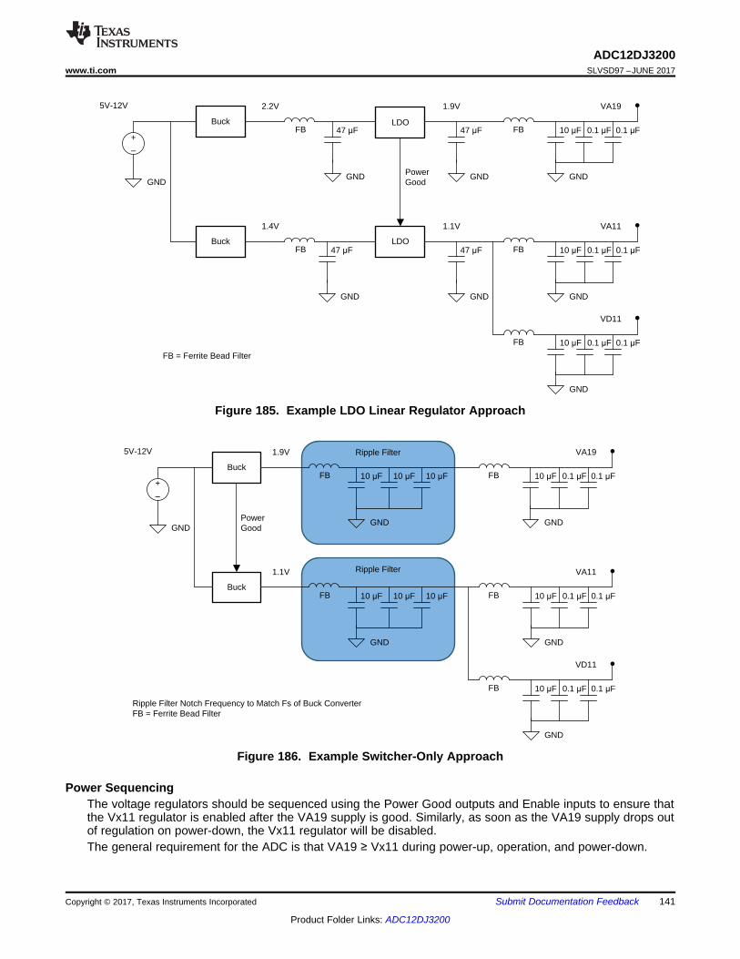
Buck10 �F 10 �F 10 �F 0.1 �F 0.1 �F
GND GND
+
±
GND
5V-12V VA19
Buck10 �F 0.1 �F 0.1 �F
GND
VA11
10 �F 0.1 �F 0.1 �F
GND
VD11
1.9V
1.1V
FB
FB FB
FB
Ripple Filter Notch Frequency to Match Fs of Buck ConverterFB = Ferrite Bead Filter
FB10 �F
10 �F 10 �F
GND
10 �F
Ripple Filter
Ripple Filter
Power Good
Buck LDO47 �F 47 �F 10 �F 0.1 �F 0.1 �F
GND GND GND
+
±
GND
5V-12V 2.2V VA19
Buck LDO47 �F 47 �F 10 �F 0.1 �F 0.1 �F
GND GND GND
1.4V VA11
10 �F 0.1 �F 0.1 �F
GND
VD11
1.9V
1.1V
FB
FB FB
FB
FB = Ferrite Bead Filter
FB
Power Good
141
ADC12DJ3200www.ti.com SLVSD97 –JUNE 2017
Product Folder Links: ADC12DJ3200
Submit Documentation FeedbackCopyright © 2017, Texas Instruments Incorporated
Figure 185. Example LDO Linear Regulator Approach
Figure 186. Example Switcher-Only Approach
Power SequencingThe voltage regulators should be sequenced using the Power Good outputs and Enable inputs to ensure thatthe Vx11 regulator is enabled after the VA19 supply is good. Similarly, as soon as the VA19 supply drops outof regulation on power-down, the Vx11 regulator will be disabled.The general requirement for the ADC is that VA19 ≥ Vx11 during power-up, operation, and power-down.

142
ADC12DJ3200SLVSD97 –JUNE 2017 www.ti.com
Product Folder Links: ADC12DJ3200
Submit Documentation Feedback Copyright © 2017, Texas Instruments Incorporated
TI also recommends that VA11 and VD11 are derived from a common 1.1-V regulator. This ensures that allof the 1.1-V blocks are at the same voltage, and no sequencing problems exist between these supplies.Ferrite bead filters should be used to isolate any noise on the VA11 and VD11 buses from affecting each-other.
10 Layout
10.1 Layout GuidelinesThere are many critical signals which require specific care during board design:1. Analog Input Signals2. CLK and SYSREF3. JESD204B Data Outputs
(a) a. Lower 8 pairs operating at up to 12.8 Gbit/sec(b) b. Upper 8 pairs operating at up to 6.4 Gbit/sec
4. Power Connections5. Ground Connections
Items 1, 2 and 3 must be routed for excellent signal quality at high frequencies. The following general practicesshould be used:1. Route using loosely coupled 100-Ω differential traces. This will minimize impact of corners and length
matching serpentines on pair impedance.2. Provide adequate pair to pair spacing to minimize crosstalk.3. Provide adequate ground plane pour spacing to minimize coupling with the high speed traces.4. Use smoothly radiused corners. Avoid 45 or 90 degree bends.5. Incorporate ground plane cutouts at component landing pads to avoid impedance discontinuities at these
locations. Cut-out below the landing pads on one or multiple ground planes to achieve a pad size/stackupheight that achieves the needed 50 ohm single ended impedance.
6. Avoid routing traces near irregularities in the reference ground planes. This includes ground planeclearances associated with power and signal vias and through-hole component leads.
7. Provide symmetrically located ground tie vias adjacent to any high speed signal vias.8. When high speed signals must transition to another layer using vias, transition as far through the board as
possible (top to bottom is best case) to minimize via stubs on top and/or bottom of the vias. If layer selectionis not flexible, use back-drilled or buried/blind vias to eliminate stubs.
In addition, TI recommends performing signal quality simulations of the critical signal traces before committing tofabrication. Insertion Loss, Return Loss and TDR (Time Domain Reflectometry) evaluations should be done.
The Power and Ground connections for the device are also very important. The following rules should befollowed:1. Provide low resistance connection paths to all power and ground pins.2. Use multiple power layers if necessary to access all pins.3. Avoid narrow isolated paths which increase the connection resistance.4. Use a Signal/Ground/Power circuit board stackup to maximum coupling between the Ground and Power
planes.
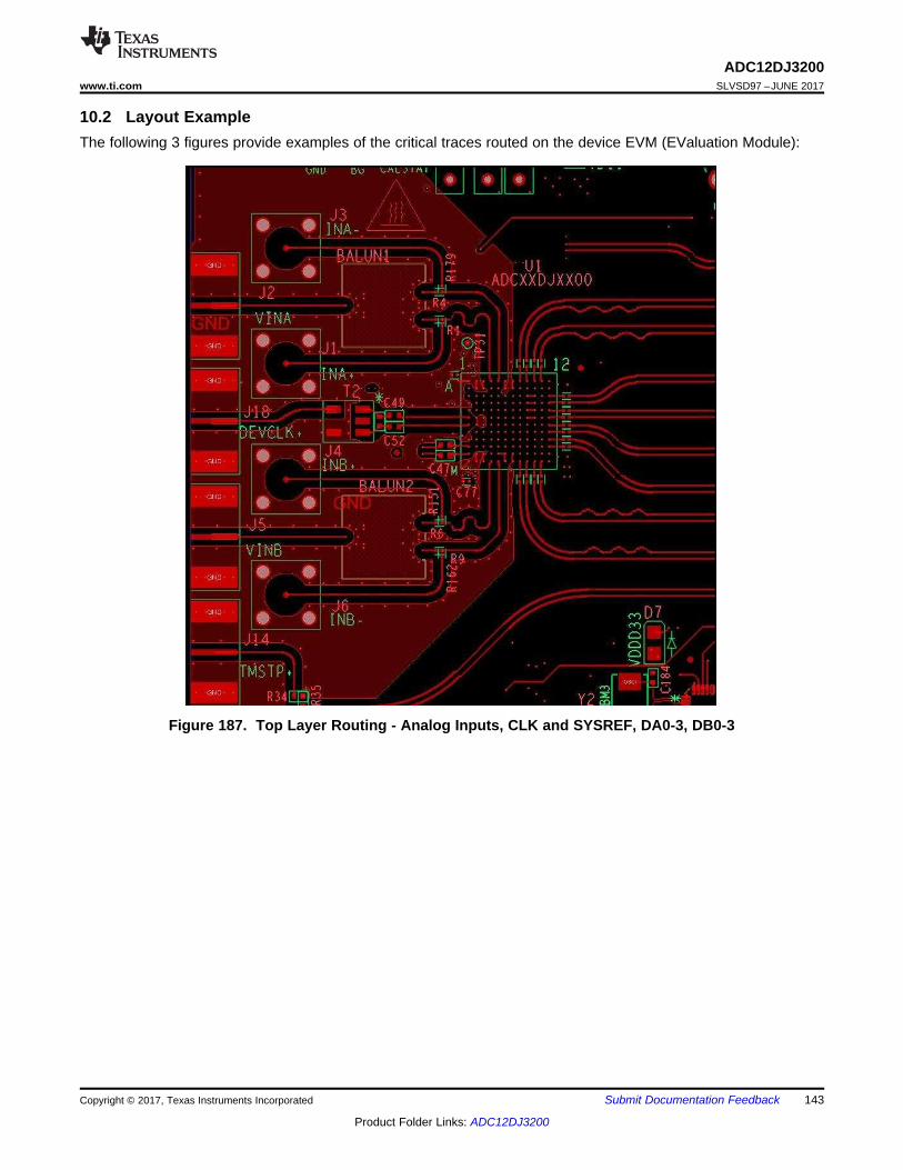
143
ADC12DJ3200www.ti.com SLVSD97 –JUNE 2017
Product Folder Links: ADC12DJ3200
Submit Documentation FeedbackCopyright © 2017, Texas Instruments Incorporated
10.2 Layout ExampleThe following 3 figures provide examples of the critical traces routed on the device EVM (EValuation Module):
Figure 187. Top Layer Routing - Analog Inputs, CLK and SYSREF, DA0-3, DB0-3

144
ADC12DJ3200SLVSD97 –JUNE 2017 www.ti.com
Product Folder Links: ADC12DJ3200
Submit Documentation Feedback Copyright © 2017, Texas Instruments Incorporated
Layout Example (continued)
Figure 188. GND1 Cutouts to Optimize Impedance of Component Pads
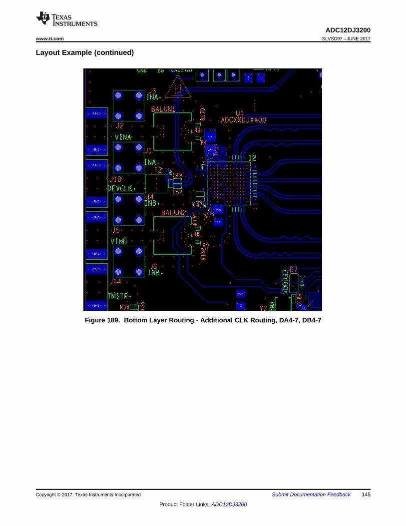
145
ADC12DJ3200www.ti.com SLVSD97 –JUNE 2017
Product Folder Links: ADC12DJ3200
Submit Documentation FeedbackCopyright © 2017, Texas Instruments Incorporated
Layout Example (continued)
Figure 189. Bottom Layer Routing - Additional CLK Routing, DA4-7, DB4-7
146
ADC12DJ3200SLVSD97 –JUNE 2017 www.ti.com
Product Folder Links: ADC12DJ3200
Submit Documentation Feedback Copyright © 2017, Texas Instruments Incorporated
11 Device and Documentation Support
11.1 Device Support
11.1.1 Third-Party Products DisclaimerTI'S PUBLICATION OF INFORMATION REGARDING THIRD-PARTY PRODUCTS OR SERVICES DOES NOTCONSTITUTE AN ENDORSEMENT REGARDING THE SUITABILITY OF SUCH PRODUCTS OR SERVICESOR A WARRANTY, REPRESENTATION OR ENDORSEMENT OF SUCH PRODUCTS OR SERVICES, EITHERALONE OR IN COMBINATION WITH ANY TI PRODUCT OR SERVICE.
11.2 Related LinksThe table below lists quick access links. Categories include technical documents, support and communityresources, tools and software, and quick access to sample or buy.
Table 148. Related Links
PARTS PRODUCT FOLDER SAMPLE & BUY TECHNICALDOCUMENTS
TOOLS &SOFTWARE
SUPPORT &COMMUNITY
ADC12DJ3200 Click here Click here Click here Click here Click here
11.3 Receiving Notification of Documentation UpdatesTo receive notification of documentation updates, navigate to the device product folder on ti.com. In the upperright corner, click on Alert me to register and receive a weekly digest of any product information that haschanged. For change details, review the revision history included in any revised document.
11.4 Community ResourcesThe following links connect to TI community resources. Linked contents are provided "AS IS" by the respectivecontributors. They do not constitute TI specifications and do not necessarily reflect TI's views; see TI's Terms ofUse.
TI E2E™ Online Community TI's Engineer-to-Engineer (E2E) Community. Created to foster collaborationamong engineers. At e2e.ti.com, you can ask questions, share knowledge, explore ideas and helpsolve problems with fellow engineers.
Design Support TI's Design Support Quickly find helpful E2E forums along with design support tools andcontact information for technical support.
11.5 TrademarksE2E is a trademark of Texas Instruments.WEBENCH is a registered trademark of Texas Instruments.
11.6 Electrostatic Discharge CautionThese devices have limited built-in ESD protection. The leads should be shorted together or the device placed in conductive foamduring storage or handling to prevent electrostatic damage to the MOS gates.
11.7 GlossarySLYZ022 — TI Glossary.
This glossary lists and explains terms, acronyms, and definitions.

147
ADC12DJ3200www.ti.com SLVSD97 –JUNE 2017
Product Folder Links: ADC12DJ3200
Submit Documentation FeedbackCopyright © 2017, Texas Instruments Incorporated
12 Mechanical, Packaging, and Orderable InformationThe following pages include mechanical, packaging, and orderable information. This information is the mostcurrent data available for the designated devices. This data is subject to change without notice and revision ofthis document. For browser-based versions of this data sheet, refer to the left-hand navigation.

PACKAGE OPTION ADDENDUM
www.ti.com 30-Jul-2017
Addendum-Page 1
PACKAGING INFORMATION
Orderable Device Status(1)
Package Type PackageDrawing
Pins PackageQty
Eco Plan(2)
Lead/Ball Finish(6)
MSL Peak Temp(3)
Op Temp (°C) Device Marking(4/5)
Samples
ADC12DJ3200AAV ACTIVE FCBGA AAV 144 1 Green (RoHS& no Sb/Br)
SNAGCU Level-3-260C-168 HR -40 to 85 ADC12DJ32
ADC12DJ3200AAVT ACTIVE FCBGA AAV 144 250 Green (RoHS& no Sb/Br)
SNAGCU Level-3-260C-168 HR -40 to 85 ADC12DJ32
(1) The marketing status values are defined as follows:ACTIVE: Product device recommended for new designs.LIFEBUY: TI has announced that the device will be discontinued, and a lifetime-buy period is in effect.NRND: Not recommended for new designs. Device is in production to support existing customers, but TI does not recommend using this part in a new design.PREVIEW: Device has been announced but is not in production. Samples may or may not be available.OBSOLETE: TI has discontinued the production of the device.
(2) RoHS: TI defines "RoHS" to mean semiconductor products that are compliant with the current EU RoHS requirements for all 10 RoHS substances, including the requirement that RoHS substancedo not exceed 0.1% by weight in homogeneous materials. Where designed to be soldered at high temperatures, "RoHS" products are suitable for use in specified lead-free processes. TI mayreference these types of products as "Pb-Free".RoHS Exempt: TI defines "RoHS Exempt" to mean products that contain lead but are compliant with EU RoHS pursuant to a specific EU RoHS exemption.Green: TI defines "Green" to mean the content of Chlorine (Cl) and Bromine (Br) based flame retardants meet JS709B low halogen requirements of <=1000ppm threshold. Antimony trioxide basedflame retardants must also meet the <=1000ppm threshold requirement.
(3) MSL, Peak Temp. - The Moisture Sensitivity Level rating according to the JEDEC industry standard classifications, and peak solder temperature.
(4) There may be additional marking, which relates to the logo, the lot trace code information, or the environmental category on the device.
(5) Multiple Device Markings will be inside parentheses. Only one Device Marking contained in parentheses and separated by a "~" will appear on a device. If a line is indented then it is a continuationof the previous line and the two combined represent the entire Device Marking for that device.
(6) Lead/Ball Finish - Orderable Devices may have multiple material finish options. Finish options are separated by a vertical ruled line. Lead/Ball Finish values may wrap to two lines if the finishvalue exceeds the maximum column width.
Important Information and Disclaimer:The information provided on this page represents TI's knowledge and belief as of the date that it is provided. TI bases its knowledge and belief on informationprovided by third parties, and makes no representation or warranty as to the accuracy of such information. Efforts are underway to better integrate information from third parties. TI has taken andcontinues to take reasonable steps to provide representative and accurate information but may not have conducted destructive testing or chemical analysis on incoming materials and chemicals.TI and TI suppliers consider certain information to be proprietary, and thus CAS numbers and other limited information may not be available for release.
In no event shall TI's liability arising out of such information exceed the total purchase price of the TI part(s) at issue in this document sold by TI to Customer on an annual basis.

PACKAGE OPTION ADDENDUM
www.ti.com 30-Jul-2017
Addendum-Page 2
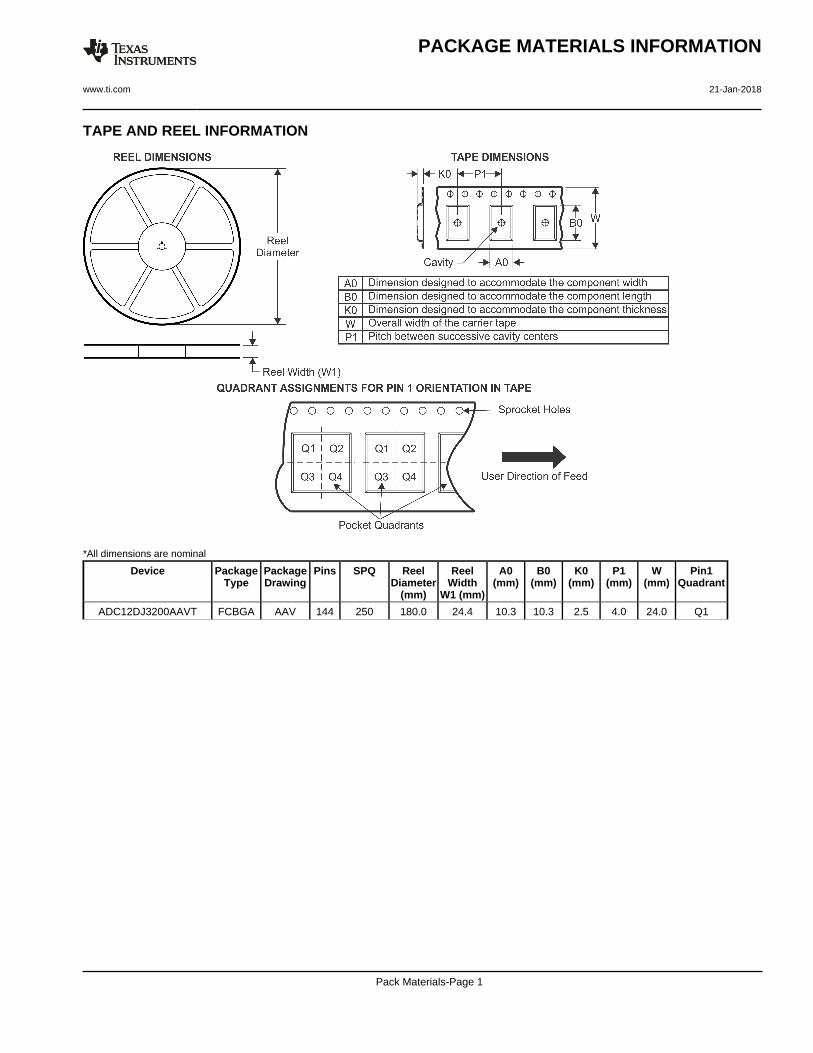
TAPE AND REEL INFORMATION
*All dimensions are nominal
Device PackageType
PackageDrawing
Pins SPQ ReelDiameter
(mm)
ReelWidth
W1 (mm)
A0(mm)
B0(mm)
K0(mm)
P1(mm)
W(mm)
Pin1Quadrant
ADC12DJ3200AAVT FCBGA AAV 144 250 180.0 24.4 10.3 10.3 2.5 4.0 24.0 Q1
PACKAGE MATERIALS INFORMATION
www.ti.com 21-Jan-2018
Pack Materials-Page 1
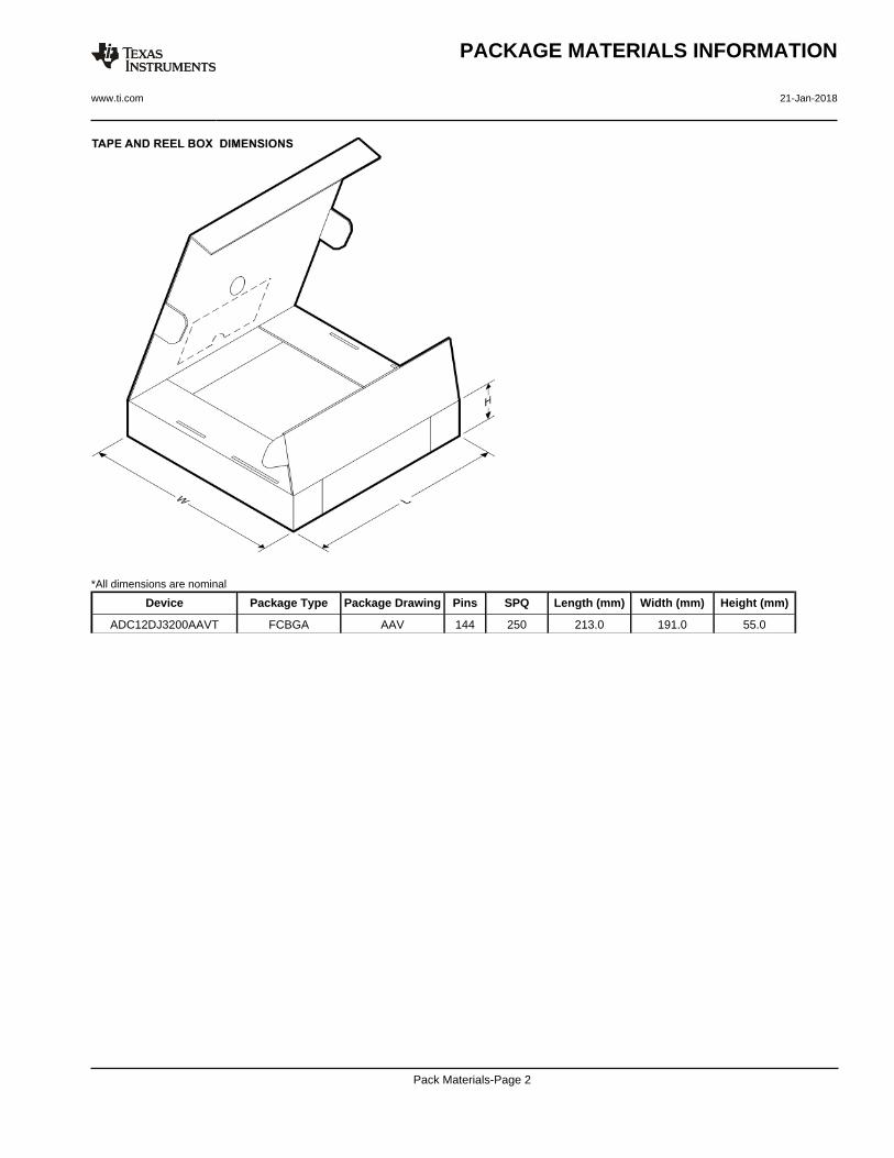
*All dimensions are nominal
Device Package Type Package Drawing Pins SPQ Length (mm) Width (mm) Height (mm)
ADC12DJ3200AAVT FCBGA AAV 144 250 213.0 191.0 55.0
PACKAGE MATERIALS INFORMATION
www.ti.com 21-Jan-2018
Pack Materials-Page 2
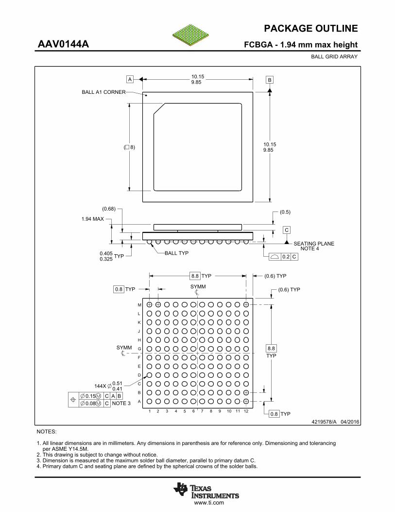
www.ti.com
PACKAGE OUTLINE
C
1.94 MAX
TYP0.4050.325
8.8TYP
8.8 TYP
0.8 TYP
0.8 TYP
144X 0.510.41
(0.68)
A 10.159.85 B
10.159.85
(0.6) TYP
( 8)
(0.5)
(0.6) TYP
FCBGA - 1.94 mm max heightAAV0144ABALL GRID ARRAY
4219578/A 04/2016
NOTES: 1. All linear dimensions are in millimeters. Any dimensions in parenthesis are for reference only. Dimensioning and tolerancing per ASME Y14.5M. 2. This drawing is subject to change without notice.3. Dimension is measured at the maximum solder ball diameter, parallel to primary datum C.4. Primary datum C and seating plane are defined by the spherical crowns of the solder balls.
BALL A1 CORNER
SEATING PLANE
BALL TYP0.2 C
NOTE 4
M
L
K
J
H
G
F
E
D
C
B
A
1 2 3
0.15 C A B0.08 C
SYMM
SYMM
4
NOTE 35 6 7 8 9 10 11 12
SCALE 1.400

www.ti.com
EXAMPLE BOARD LAYOUT
144X ( )0.4
(0.8) TYP
(0.8) TYP
( )METAL
0.4 0.05 MAX
SOLDER MASKOPENING
METAL UNDERSOLDER MASK
( )SOLDER MASKOPENING
0.4
0.05 MIN
FCBGA - 1.94 mm max heightAAV0144ABALL GRID ARRAY
4219578/A 04/2016
NOTES: (continued) 5. Final dimensions may vary due to manufacturing tolerance considerations and also routing constraints. For more information, see Texas Instruments literature number SPRU811 (www.ti.com/lit/spru811).
SYMM
SYMM
LAND PATTERN EXAMPLESCALE:8X
1A
B
C
D
E
F
G
H
J
K
L
M
2 3 4 5 6 7 8 9 10 11 12
NON-SOLDER MASKDEFINED
(PREFERRED)
SOLDER MASK DETAILSNOT TO SCALE
SOLDER MASKDEFINED

www.ti.com
EXAMPLE STENCIL DESIGN
(0.8)TYP
(0.8) TYP 144X ( )0.4
FCBGA - 1.94 mm max heightAAV0144ABALL GRID ARRAY
4219578/A 04/2016
NOTES: (continued) 6. Laser cutting apertures with trapezoidal walls and rounded corners may offer better paste release.
SOLDER PASTE EXAMPLEBASED ON 0.15 mm THICK STENCIL
SCALE:8X
SYMM
SYMM
1A
B
C
D
E
F
G
H
J
K
L
M
2 3 4 5 6 7 8 9 10 11 12

IMPORTANT NOTICE
Texas Instruments Incorporated (TI) reserves the right to make corrections, enhancements, improvements and other changes to itssemiconductor products and services per JESD46, latest issue, and to discontinue any product or service per JESD48, latest issue. Buyersshould obtain the latest relevant information before placing orders and should verify that such information is current and complete.TI’s published terms of sale for semiconductor products (http://www.ti.com/sc/docs/stdterms.htm) apply to the sale of packaged integratedcircuit products that TI has qualified and released to market. Additional terms may apply to the use or sale of other types of TI products andservices.Reproduction of significant portions of TI information in TI data sheets is permissible only if reproduction is without alteration and isaccompanied by all associated warranties, conditions, limitations, and notices. TI is not responsible or liable for such reproduceddocumentation. Information of third parties may be subject to additional restrictions. Resale of TI products or services with statementsdifferent from or beyond the parameters stated by TI for that product or service voids all express and any implied warranties for theassociated TI product or service and is an unfair and deceptive business practice. TI is not responsible or liable for any such statements.Buyers and others who are developing systems that incorporate TI products (collectively, “Designers”) understand and agree that Designersremain responsible for using their independent analysis, evaluation and judgment in designing their applications and that Designers havefull and exclusive responsibility to assure the safety of Designers' applications and compliance of their applications (and of all TI productsused in or for Designers’ applications) with all applicable regulations, laws and other applicable requirements. Designer represents that, withrespect to their applications, Designer has all the necessary expertise to create and implement safeguards that (1) anticipate dangerousconsequences of failures, (2) monitor failures and their consequences, and (3) lessen the likelihood of failures that might cause harm andtake appropriate actions. Designer agrees that prior to using or distributing any applications that include TI products, Designer willthoroughly test such applications and the functionality of such TI products as used in such applications.TI’s provision of technical, application or other design advice, quality characterization, reliability data or other services or information,including, but not limited to, reference designs and materials relating to evaluation modules, (collectively, “TI Resources”) are intended toassist designers who are developing applications that incorporate TI products; by downloading, accessing or using TI Resources in anyway, Designer (individually or, if Designer is acting on behalf of a company, Designer’s company) agrees to use any particular TI Resourcesolely for this purpose and subject to the terms of this Notice.TI’s provision of TI Resources does not expand or otherwise alter TI’s applicable published warranties or warranty disclaimers for TIproducts, and no additional obligations or liabilities arise from TI providing such TI Resources. TI reserves the right to make corrections,enhancements, improvements and other changes to its TI Resources. TI has not conducted any testing other than that specificallydescribed in the published documentation for a particular TI Resource.Designer is authorized to use, copy and modify any individual TI Resource only in connection with the development of applications thatinclude the TI product(s) identified in such TI Resource. NO OTHER LICENSE, EXPRESS OR IMPLIED, BY ESTOPPEL OR OTHERWISETO ANY OTHER TI INTELLECTUAL PROPERTY RIGHT, AND NO LICENSE TO ANY TECHNOLOGY OR INTELLECTUAL PROPERTYRIGHT OF TI OR ANY THIRD PARTY IS GRANTED HEREIN, including but not limited to any patent right, copyright, mask work right, orother intellectual property right relating to any combination, machine, or process in which TI products or services are used. Informationregarding or referencing third-party products or services does not constitute a license to use such products or services, or a warranty orendorsement thereof. Use of TI Resources may require a license from a third party under the patents or other intellectual property of thethird party, or a license from TI under the patents or other intellectual property of TI.TI RESOURCES ARE PROVIDED “AS IS” AND WITH ALL FAULTS. TI DISCLAIMS ALL OTHER WARRANTIES ORREPRESENTATIONS, EXPRESS OR IMPLIED, REGARDING RESOURCES OR USE THEREOF, INCLUDING BUT NOT LIMITED TOACCURACY OR COMPLETENESS, TITLE, ANY EPIDEMIC FAILURE WARRANTY AND ANY IMPLIED WARRANTIES OFMERCHANTABILITY, FITNESS FOR A PARTICULAR PURPOSE, AND NON-INFRINGEMENT OF ANY THIRD PARTY INTELLECTUALPROPERTY RIGHTS. TI SHALL NOT BE LIABLE FOR AND SHALL NOT DEFEND OR INDEMNIFY DESIGNER AGAINST ANY CLAIM,INCLUDING BUT NOT LIMITED TO ANY INFRINGEMENT CLAIM THAT RELATES TO OR IS BASED ON ANY COMBINATION OFPRODUCTS EVEN IF DESCRIBED IN TI RESOURCES OR OTHERWISE. IN NO EVENT SHALL TI BE LIABLE FOR ANY ACTUAL,DIRECT, SPECIAL, COLLATERAL, INDIRECT, PUNITIVE, INCIDENTAL, CONSEQUENTIAL OR EXEMPLARY DAMAGES INCONNECTION WITH OR ARISING OUT OF TI RESOURCES OR USE THEREOF, AND REGARDLESS OF WHETHER TI HAS BEENADVISED OF THE POSSIBILITY OF SUCH DAMAGES.Unless TI has explicitly designated an individual product as meeting the requirements of a particular industry standard (e.g., ISO/TS 16949and ISO 26262), TI is not responsible for any failure to meet such industry standard requirements.Where TI specifically promotes products as facilitating functional safety or as compliant with industry functional safety standards, suchproducts are intended to help enable customers to design and create their own applications that meet applicable functional safety standardsand requirements. Using products in an application does not by itself establish any safety features in the application. Designers mustensure compliance with safety-related requirements and standards applicable to their applications. Designer may not use any TI products inlife-critical medical equipment unless authorized officers of the parties have executed a special contract specifically governing such use.Life-critical medical equipment is medical equipment where failure of such equipment would cause serious bodily injury or death (e.g., lifesupport, pacemakers, defibrillators, heart pumps, neurostimulators, and implantables). Such equipment includes, without limitation, allmedical devices identified by the U.S. Food and Drug Administration as Class III devices and equivalent classifications outside the U.S.TI may expressly designate certain products as completing a particular qualification (e.g., Q100, Military Grade, or Enhanced Product).Designers agree that it has the necessary expertise to select the product with the appropriate qualification designation for their applicationsand that proper product selection is at Designers’ own risk. Designers are solely responsible for compliance with all legal and regulatoryrequirements in connection with such selection.Designer will fully indemnify TI and its representatives against any damages, costs, losses, and/or liabilities arising out of Designer’s non-compliance with the terms and provisions of this Notice.
Mailing Address: Texas Instruments, Post Office Box 655303, Dallas, Texas 75265Copyright © 2018, Texas Instruments Incorporated


![Channel Structure and Function [Compatibility Mode]](https://static.fdocuments.us/doc/165x107/577cc0f01a28aba71191a8b0/channel-structure-and-function-compatibility-mode.jpg)