ADAM81P12XX User’s Manual - abov.co.kr · adam81p12xx user's manual ... r02/ks2/an2...
109
A D Am ® Advanced Design Advanced Microcontroller Understanding of ADAM81 Series Architecture A Guide to ADAM81P12XX ADAM81P12XX User’s Manual (V0.8-2010.05) www.etachips.com Copyright(c) 2009 ETA CHIPS Co. All rights reserved. Questions and Informations, please send a mail to [email protected] eta chips co.
Transcript of ADAM81P12XX User’s Manual - abov.co.kr · adam81p12xx user's manual ... r02/ks2/an2...

ADAm®
Advanced DesignAdvanced Microcontroller
Understanding ofADAM81 Series Architecture
A Guide to
ADAM81P12XXADAM81P12XX
User’s Manual
(V0.8-2010.05)
www.etachips.com
Copyright(c) 2009 ETA CHIPS Co. All rights reserved.Questions and Informations, please send a mail to [email protected]
eta chips co.

ADAm®
Advanced DesignAdvanced Microcontroller
0. User’s Manual Revision History
8. [V0.8-2010.05] 1.7.3. DC Characteristics (DC Current Value is modified.)
7. [V0.7-2009.11] Code Option Bit Default value define.
6. [V0.6-2009.07] R3FN2 function is modified.
5. [V0.5-2009.07] Code Option Bit Mapping is modified. Internal RC-OSC Spec is modified.
4. [V0.4-2009.02] 12. Voltage Detection Indicator Mode
12.3. Timming Diagram (VDI RESET mode, Must set (ENST=1))
3. [V0.3-2008.12] 1.7.3. DC Characteristics
DC Current Value is modified.
2. [V0.2-2008.11] 1.7.3. DC Characteristics
VOH/VOL Typ. Value is modified as 0.7v <- 0.4v .
1 [V0 1 2008 11]1. [V0.1-2008.11] 2.7 Peripheral Registers
*bit is read-modified operation. (SETR1/CLRR1 instruction)
0. [V0.0-2008.10] 1’st release
1ADAM81P12XX User's Manual (V0.8-2010.05)

ADAm®
Advanced DesignAdvanced Microcontroller
1. OVERVIEW
The ADAM81 is the High Speed and Low Voltage operating 8-bit single chip microcomputer. The ADAM81 contains ADAM80 CPU, RAM, Timer/PWM, Interrupt, Watch Dog Timer, 12-bit ADC, I t/O t t P t d O ill ti Ci itInput/Output Ports and Oscillation Circuit.
1.1. Features
High Performance 8-bit RISC CPU 55 - Instructions (most single cycle) General Purpose Registers 8bit x 8
(A, B, C, D, E, F, G, H) Program Stack Level 16 level Interrupt Stack Level 8 level
SRAM I di t Add i R i t (X A) 8bit 1 (Add i 192b t ) SRAM Indirect Addressing Register (X, A) 8bit x 1 (Addressing 192bytes)SRAM Indirect Addressing Pointer (Y) 5bit x 1 (Addressing 32bytes)
Instruction Execution Time 0.5us @8MHz Program Memory Area 8K bytes (4K x 16bit) Data Memory Area 192bytes Timer 16bit x 3ch [PWM: (8+8)bit x 3ch]
(Include function : Timer/PWM/Counter/Capture) Watch-Dog Timer (with RCWDT=32us) 19bit Interrupt Source External 4ch
(KS, INT0, INT1, INT2)Internal 6ch (T0, T1, T2, ADC, WDT, VDI)
Analog-Digital Converter 12bit x 12ch Internal RCOSC typ. 16/8/4/2/1MHz Internal RCWDT typ. 32KHz External R-OSC Power Saving Operation Modes STOP, SLEEP, RC-WDT Power-On Reset Low Voltage Detector Voltage Detection Indicator 3 level (2.3V/3.0V/3.8V) Operating Voltage 1.8V ~ 5.5V @(1 ~ 4MHz, 32KHz)
2.2V ~ 5.5V @(1 ~ 8MHz)2.7V ~ 5.5V @(1 ~ 20MHz)
Operating Temperature -40OC ~ 85OC Package 20/16 SOP
Series ADAM81P1220 ADAM81P1216
ADAM81P12XX Series members
Program memory 4,096 x 16 4,096 x 16
Data memory 192 x 8 192 x 8
I/O ports (max.) *14 (18) *10 (14)
Package 20SOP 16SOP
* OSC1/OSC2/RESETB/VREF
2ADAM81P12XX User's Manual (V0.8-2010.05)

ADAm®
Advanced DesignAdvanced Microcontroller
1. OVERVIEW
1.2. Pin Assignments
2019181716
123456
AD
AM
81
(20
-S
VDDR00/KS0/AN0/INT0(EC0)/SCKR01/KS1/AN1/INT1(EC1)/VREF/SDAR02/KS2/AN2R10/KS7/AN7/INT2(EC2)
GNDOSC1/R30OSC2/R31
VPP/RESETB/R32T2/R20
1514131211
678910
1P
122
0SO
P)
R11/KS8/AN8R12/KS9/AN9/T1R13/KS10/AN10/T0R14/KS11/AN11R15/KS12/AN12/CLO
TM12/R21TM01/R22AN13/R23AN14/R24AN15/R25
161514131211
123456
AD
AM
81
P1
2(1
6-SO
P)
VDDR00/KS0/AN0/INT0(EC0)/SCKR01/KS1/AN1/INT1(EC1)/VREF/SDAR02/KS2/AN2R10/KS7/AN7/INT2(EC2)R11/KS8/AN8
GNDOSC1/R30OSC2/R31
VPP/RESETB/R32T2/R20
TM12/R21 11109
678
216
) R11/KS8/AN8R12/KS9/AN9/T1R13/KS10/AN10/T0
TM12/R21TM01/R22AN13/R23
A
8765
1234
AD
AM
81
P1
208
(8-SO
P)
VDDR00/KS0/AN0/INT0(EC0)/SCKR01/KS1/AN1/INT1(EC1)/VREF/SDAR02/KS2/AN2
GNDOSC1/R30OSC2/R31
VPP/RESETB/R32
3ADAM81P12XX User's Manual (V0.8-2010.05)
ADAm®
Advanced DesignAdvanced Microcontroller
1. OVERVIEW
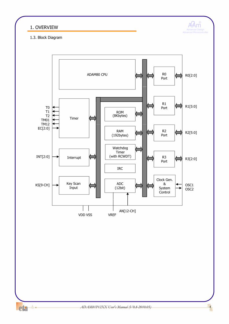
1.3. Block Diagram
R0[2:0]ADAM80 CPU R0Port
Timer
R1Port
ROM(8Kbytes)
R1[5:0]T0T1T2
TM01TM12
RAM(192bytes)
Interrupt
R2Port
R3Port
R3[2:0]
R2[5:0]
TM12EC[2:0]
INT[2:0]
WatchdogTimer
(with RCWDT)
KS[9-CH] Key Scan Input
Clock Gen.&
SystemControl
Port
ADC(12bit)
IRC
OSC1OSC2
VDD VSSAN[12-CH]
VREF
4ADAM81P12XX User's Manual (V0.8-2010.05)
ADAm®
Advanced DesignAdvanced Microcontroller
1. OVERVIEW
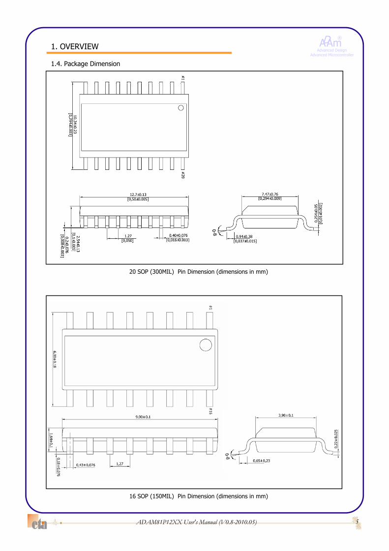
1.4. Package Dimension
20 SOP (300MIL) Pin Dimension (dimensions in mm)
5ADAM81P12XX User's Manual (V0.8-2010.05)
16 SOP (150MIL) Pin Dimension (dimensions in mm)

ADAm®
Advanced DesignAdvanced Microcontroller
1. OVERVIEW
Pin Name I/O Function @RESET @STOP
1.5. Pin Function
Pin Name I/O Function @RESET @STOP
R02/KS2/AN2R01/KS1/AN1/INT1(EC1)/VREF
R00/KS0/AN0/INT0(EC0)I/O
- 3-bit I/O Port.- CMOS input with pull-up resistor.- Push-pull output. - Each pin can be set and reset by Data register value.- Can be programmable as Pull-up/N-ch open drain/KS/AN/INT(EC).- Direct Driving of LED.
InputState
of beforeSTOP
g
R15/KS12/CLOR14/KS11
R13/KS10/AN10/T0R12/KS9/AN9/T1
R11/KS8/AN8R10/KS7/AN7/INT2(EC2)
I/O
- 6-bit I/O Port.- CMOS input with pull-up resistor.- Push-pull output. - Each pin can be set and reset by Data register value.- Can be programmable as Pull-up/N-ch open drain/KS/AN/INT(EC)/TIMER/CLO.- Direct Driving of LED.
InputState
of beforeSTOP
R25/AN15R24/AN14R23/AN13R22/TM01R21/TM12
R20/T2
I/O
- 8-bit I/O Port.- CMOS input with pull-up resistor.- Push-pull output. - Each pin can be set and reset by Data register value.- Can be programmable as Pull-up/N-ch open drain/AN/TIMER.- Direct Driving of LED.
InputState
of beforeSTOP
3 bit I/O Port
R32/RESETBR31/OSC2R30/OSC1
I/O
- 3-bit I/O Port.- CMOS input with pull-up resistor.- Push-pull output. - Each pin can be set and reset by Data register value.- Can be programmable as Pull-up/Pull-down/N-ch open drain.- R32 is open-drain output.- Direct Driving of LED.
InputState
of beforeSTOP
RESETB I - External RESETB Input by Code/Register Option. Input
OSC1 I - Oscillator Input. Input Low
OSC2 O - Oscillator Output. Output High
VREF P - ADC Positive Power Supply.
VDD P - Positive Power Supply.
GND P - Ground.
6ADAM81P12XX User's Manual (V0.8-2010.05)

ADAm®
Advanced DesignAdvanced Microcontroller
1. OVERVIEW
Pin Name Circuit Type RESET
1.6. Port Structure (Normal I/O mode with Pull-Up & Open-Drain)
Pin Name Circuit Type RESET
R0[2:0]D t R i t
Open drain Selection VDD
VDD
Pull-up Selection Pull upresistor
R1[5:0]R2[5:0]R3[2:0]
Input
Direction Register
Data Bus
PortData Register
MUX
GND
Rd
1
0
SharedFunction KS/AN/INT(EC)/VREF/TIMER/CLO/OSC1/OSC2
Assignment Direction Pull-UpPort Read
Port Remarks RESETDir. Input Dir. Output
KS Input * Port Data KS
Rd
KS Input * Port Data KS
AN Input Off Port(Analog Input)=unknown= Data AN
INT(EC) Input * Port Data INT(EC)
VREF Input Off Port(Analog Power)=unknown=
Port(Analog Power)=unknown= VREF R0[1] RESET
TIMER Output Off Port Data TIMER
CLO Output Off Port Data CLO
* : It is depend on user definition.
7ADAM81P12XX User's Manual (V0.8-2010.05)

ADAm®
Advanced DesignAdvanced Microcontroller
1. OVERVIEW
1.6. Port Structure (RESETB mode)
Pin Name Circuit Type RESET
Reset Selection
Port
VDD
Pull-up Selection Pull upresistor
R3[2] Input
Data Bus
Data RegisterGND
Rd
MUX1
0
Direction Register
SharedFunction RESETB (Input with Pull-up)
Port Read
System RESET
Assignment Direction Pull-UpPort Read
Port Remarks RESETDir. Input -
RESETB Input On Port - Pull-upRESETB R3[2] RESET
8ADAM81P12XX User's Manual (V0.8-2010.05)
ADAm®
Advanced DesignAdvanced Microcontroller
Pin Name Circuit Type RESET
1. OVERVIEW
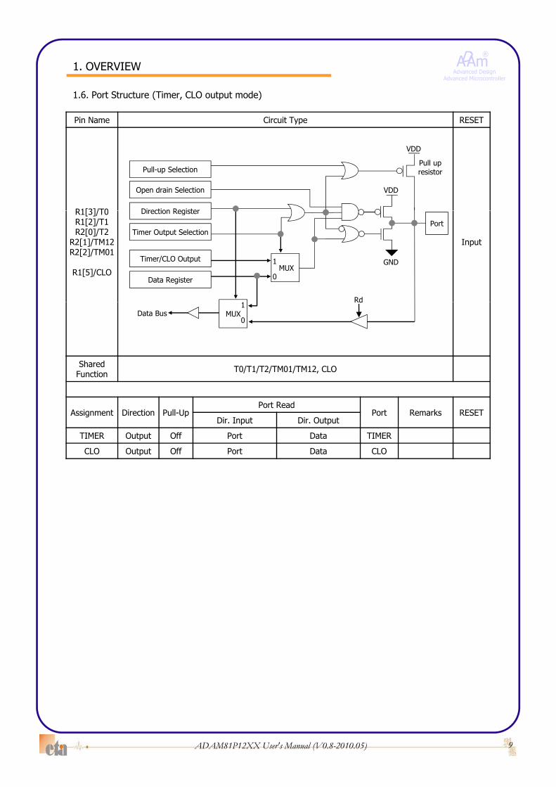
1.6. Port Structure (Timer, CLO output mode)
Pin Name Circuit Type RESET
R1[3]/T0 Direction Register
Open drain Selection VDD
VDD
Pull-up SelectionPull upresistor
R1[3]/T0R1[2]/T1R2[0]/T2
R2[1]/TM12R2[2]/TM01
R1[5]/CLO
Input
Direction Register
Port
Timer/CLO Output GND
Rd
Timer Output Selection
Data Register
MUX1
0
SharedFunction T0/T1/T2/TM01/TM12, CLO
Data Bus
Rd
MUX1
0
Assignment Direction Pull-UpPort Read
Port Remarks RESETDir. Input Dir. Output
TIMER Output Off Port Data TIMER
CLO Output Off Port Data CLO
9ADAM81P12XX User's Manual (V0.8-2010.05)
ADAm®
Advanced DesignAdvanced Microcontroller
Pin Name Circuit Type RESET
1. OVERVIEW
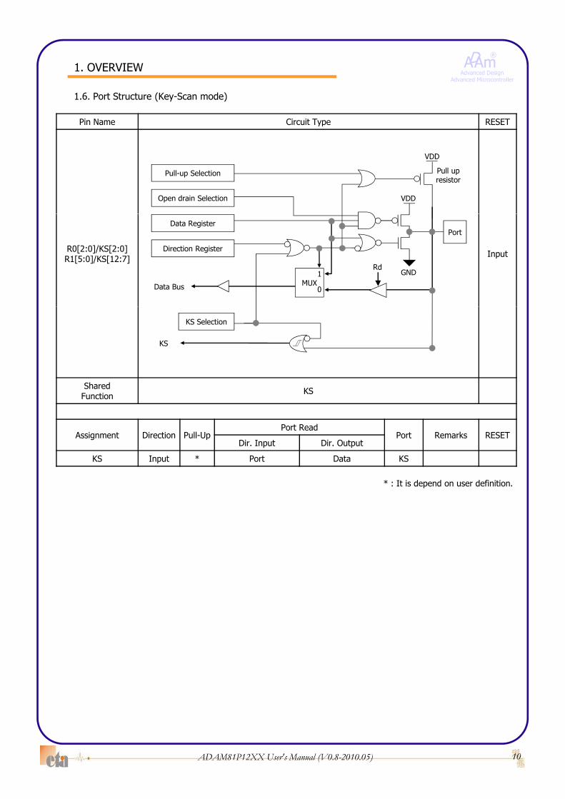
1.6. Port Structure (Key-Scan mode)
Pin Name Circuit Type RESET
Open drain Selection VDD
VDD
Pull-up Selection Pull upresistor
R0[2:0]/KS[2:0]R1[5:0]/KS[12:7] Input
Direction Register
Data Bus
PortData Register
MUXGND
Rd1
0
SharedFunction KS
KS Selection
KS
Function
Assignment Direction Pull-UpPort Read
Port Remarks RESETDir. Input Dir. Output
KS Input * Port Data KS
* : It is depend on user definition.
10ADAM81P12XX User's Manual (V0.8-2010.05)
ADAm®
Advanced DesignAdvanced Microcontroller
Pin Name Circuit Type RESET
1. OVERVIEW
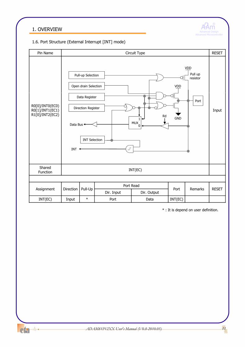
1.6. Port Structure (External Interrupt [INT] mode)
Pin Name Circuit Type RESET
Open drain Selection VDD
VDD
Pull-up Selection Pull upresistor
R0[0]/INT0(EC0)R0[1]/INT1(EC1)R1[0]/INT2(EC2)
InputDirection Register
Data Bus
PortData Register
MUXGND
Rd1
0
SharedFunction INT(EC)
INT Selection
INT
Function
Assignment Direction Pull-UpPort Read
Port Remarks RESETDir. Input Dir. Output
INT(EC) Input * Port Data INT(EC)
* : It is depend on user definition.
11ADAM81P12XX User's Manual (V0.8-2010.05)

ADAm®
Advanced DesignAdvanced Microcontroller
Pin Name Circuit Type RESET
1. OVERVIEW
1.6. Port Structure (Analog Input [AN] mode)
Pin Name Circuit Type RESET
Open drain Selection VDD
VDD
Pull-up Selection Pull upresistor
R0[2:0]/AN[2:0]R1[5:0]/AN[12:7]R2[5:3]/AN[15:13]
InputDirection Register
Data Bus
PortData Register
MUXGND
Rd1
0
Sh d
AN SelectionCHSEL
AN
SharedFunction AN
Assignment Direction Pull-UpPort Read
Port Remarks RESETDir. Input Dir. Output
AN Input Off Port(Analog Input)=unknown= Data AN
* : It is depend on user definition.
12ADAM81P12XX User's Manual (V0.8-2010.05)
ADAm®
Advanced DesignAdvanced Microcontroller
Pin Name Circuit Type RESET
1. OVERVIEW
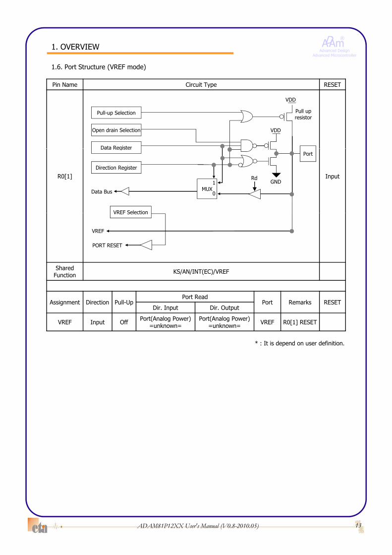
1.6. Port Structure (VREF mode)
Pin Name Circuit Type RESET
Data Register
Open drain Selection VDD
VDD
Pull-up Selection Pull upresistor
R0[1] InputDirection Register
Data Bus
PortData Register
MUXGND
Rd1
0
VREF Selection
SharedFunction KS/AN/INT(EC)/VREF
VREF Selection
VREF
PORT RESET
Function
Assignment Direction Pull-UpPort Read
Port Remarks RESETDir. Input Dir. Output
VREF Input Off Port(Analog Power)=unknown=
Port(Analog Power)=unknown= VREF R0[1] RESET
* It i d d d fi iti* : It is depend on user definition.
13ADAM81P12XX User's Manual (V0.8-2010.05)

ADAm®
Advanced DesignAdvanced Microcontroller
1. OVERVIEW
Pin Name Circuit Type RESET
1.6. Port Structure (Normal I/O mode with Pull-Down)
Pin Name Circuit Type RESET
D t R i t
Open drain Selection VDD
VDD
Pull-up Selection Pull upresistor
R3[0]/OSC1R3[1]/OSC2 Input
Direction Register
Data Bus
PortData Register
MUX
GND
Rd
1
0Direction
Input
SharedF ti OSC1/OSC2
Rd
Pull downresistorPull-down Selection
GND
Input
Function OSC1/OSC2
Assignment Direction Pull-UpPort Read
Port Remarks RESETDir. Input Dir. Output
OSC1 Input Off =unknown= =unknown= OSC1 R3[0] RESET
DisableOSC2 Input Off =unknown= =unknown= OSC2 R3[1] RESET
Pull-down Input * * * *
* : It is depend on user definition.
14ADAM81P12XX User's Manual (V0.8-2010.05)
ADAm®
Advanced DesignAdvanced Microcontroller
1. OVERVIEW
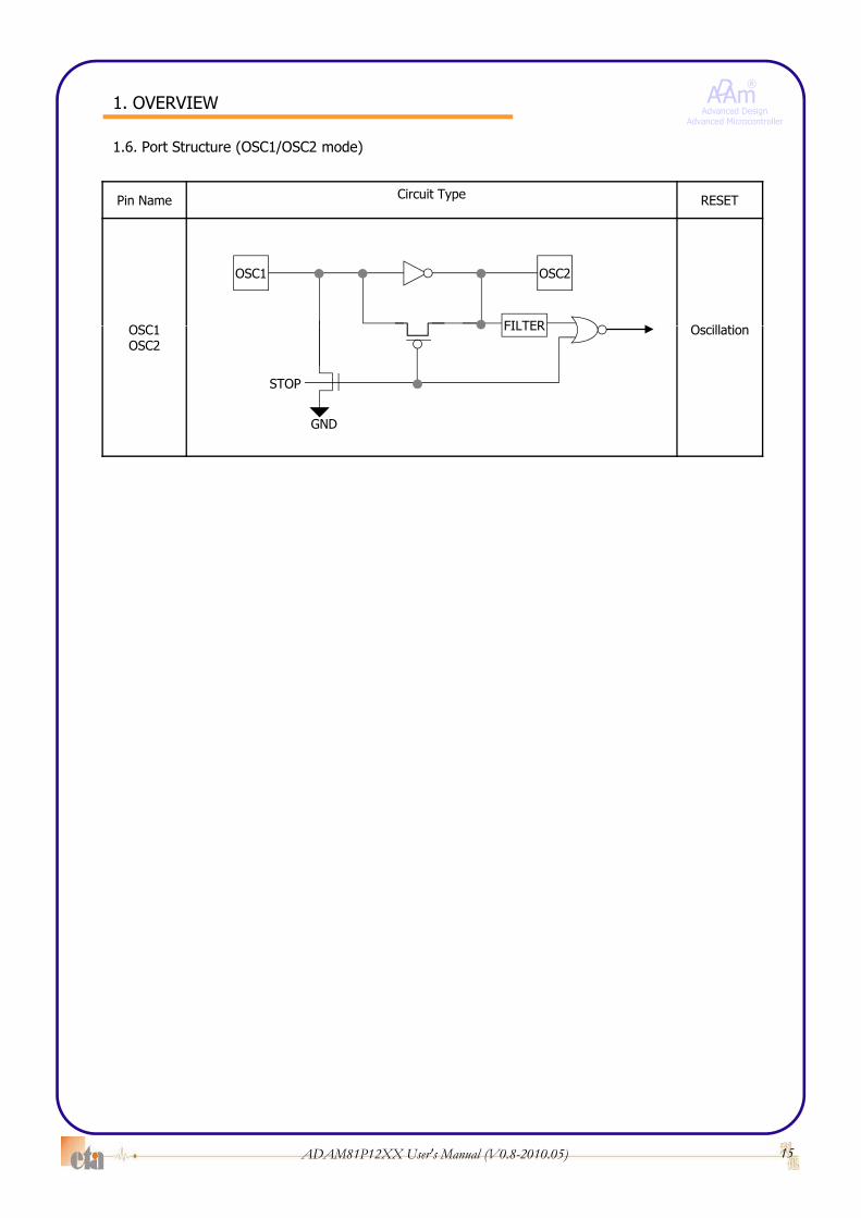
1.6. Port Structure (OSC1/OSC2 mode)
Pin Name Circuit Type RESET
OSC1 O ill ti
OSC1 OSC2
FILTEROSC1OSC2
Oscillation
GND
STOP
FILTER
15ADAM81P12XX User's Manual (V0.8-2010.05)
ADAm®
Advanced DesignAdvanced Microcontroller
1. OVERVIEW
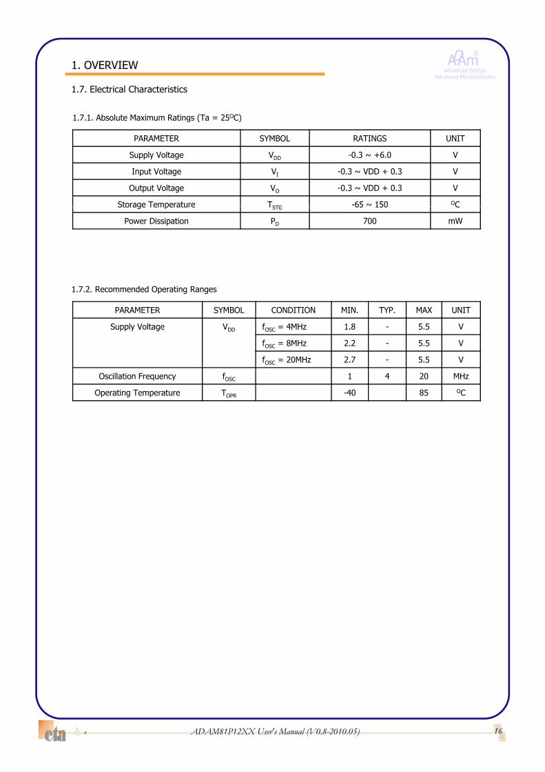
1 7 1 Absolute Maximum Ratings (Ta = 25OC)
1.7. Electrical Characteristics
1.7.1. Absolute Maximum Ratings (Ta = 25OC)
PARAMETER SYMBOL RATINGS UNIT
Supply Voltage VDD -0.3 ~ +6.0 V
Input Voltage VI -0.3 ~ VDD + 0.3 V
Output Voltage VO -0.3 ~ VDD + 0.3 V
Storage Temperature TSTG -65 ~ 150 OC
1.7.2. Recommended Operating Ranges
Storage Temperature TSTG 65 150 C
Power Dissipation PD 700 mW
PARAMETER SYMBOL CONDITION MIN. TYP. MAX UNIT
Supply Voltage VDD fOSC = 4MHz 1.8 - 5.5 V
fOSC = 8MHz 2.2 - 5.5 V
fOSC = 20MHz 2.7 - 5.5 V
Oscillation Frequency fOSC 1 4 20 MHz
Operating Temperature TOPR -40 85 OC
16ADAM81P12XX User's Manual (V0.8-2010.05)
ADAm®
Advanced DesignAdvanced Microcontroller
1. OVERVIEW
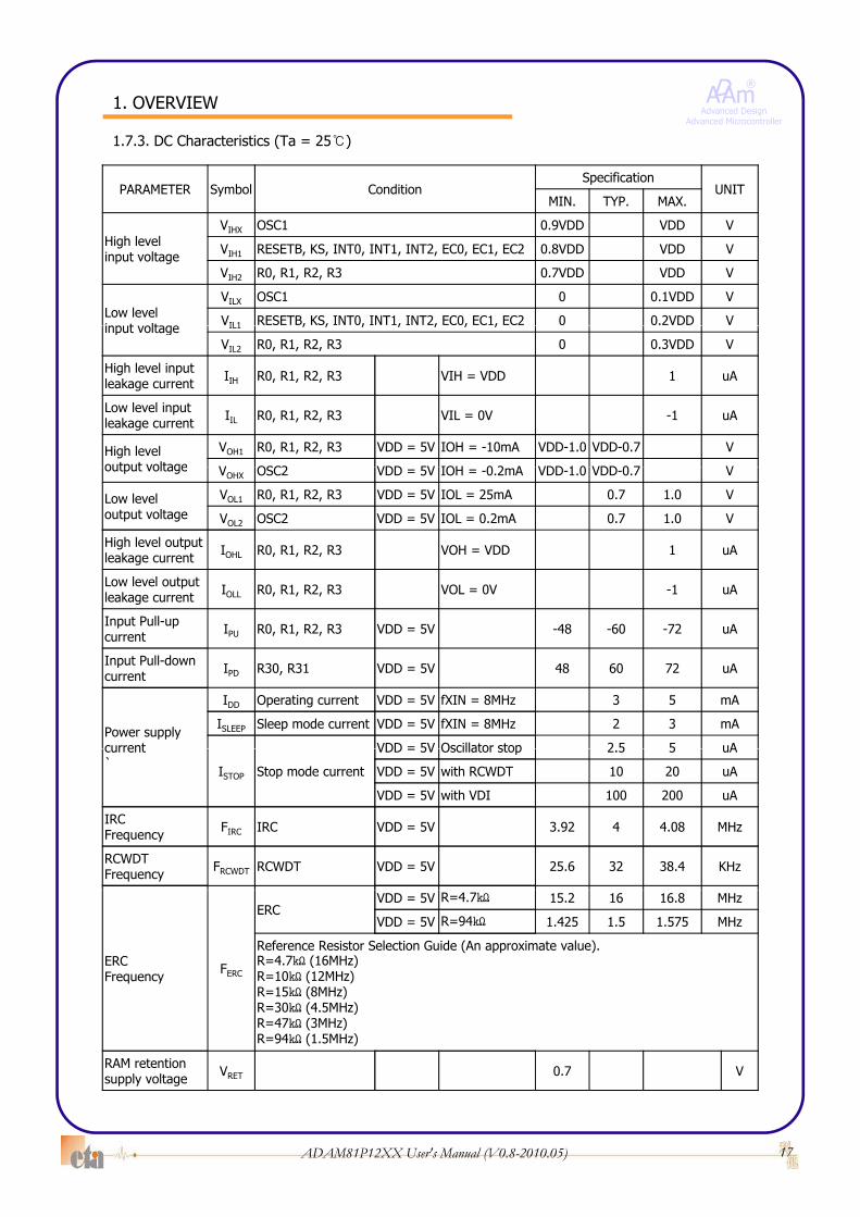
1.7.3. DC Characteristics (Ta = 25℃)
PARAMETER S b l C di iSpecification
UNITPARAMETER Symbol Condition UNITMIN. TYP. MAX.
High levelinput voltage
VIHX OSC1 0.9VDD VDD V
VIH1 RESETB, KS, INT0, INT1, INT2, EC0, EC1, EC2 0.8VDD VDD V
VIH2 R0, R1, R2, R3 0.7VDD VDD V
Low levelinput voltage
VILX OSC1 0 0.1VDD V
VIL1 RESETB, KS, INT0, INT1, INT2, EC0, EC1, EC2 0 0.2VDD Vinput voltage IL1 , , , , , , ,
VIL2 R0, R1, R2, R3 0 0.3VDD V
High level inputleakage current IIH R0, R1, R2, R3 VIH = VDD 1 uA
Low level inputleakage current IIL R0, R1, R2, R3 VIL = 0V -1 uA
High leveloutput voltage
VOH1 R0, R1, R2, R3 VDD = 5V IOH = -10mA VDD-1.0 VDD-0.7 V
V OSC2 VDD 5V IOH 0 2 A VDD 1 0 VDD 0 7 Voutput voltage VOHX OSC2 VDD = 5V IOH = -0.2mA VDD-1.0 VDD-0.7 V
Low leveloutput voltage
VOL1 R0, R1, R2, R3 VDD = 5V IOL = 25mA 0.7 1.0 V
VOL2 OSC2 VDD = 5V IOL = 0.2mA 0.7 1.0 V
High level outputleakage current IOHL R0, R1, R2, R3 VOH = VDD 1 uA
Low level outputleakage current IOLL R0, R1, R2, R3 VOL = 0V -1 uA
Input Pull-upcurrent IPU R0, R1, R2, R3 VDD = 5V -48 -60 -72 uA
Input Pull-downcurrent IPD R30, R31 VDD = 5V 48 60 72 uA
Power supplycurrent
IDD Operating current VDD = 5V fXIN = 8MHz 3 5 mA
ISLEEP Sleep mode current VDD = 5V fXIN = 8MHz 2 3 mA
VDD = 5V Oscillator stop 2 5 5 uAcurrent`
ISTOP Stop mode current
VDD = 5V Oscillator stop 2.5 5 uA
VDD = 5V with RCWDT 10 20 uA
VDD = 5V with VDI 100 200 uA
IRCFrequency FIRC IRC VDD = 5V 3.92 4 4.08 MHz
RCWDT Frequency FRCWDT RCWDT VDD = 5V 25.6 32 38.4 KHz
ERCFrequency FERC
ERCVDD = 5V R=4.7㏀ 15.2 16 16.8 MHz
VDD = 5V R=94㏀ 1.425 1.5 1.575 MHz
Reference Resistor Selection Guide (An approximate value).R=4.7㏀ (16MHz)R=10㏀ (12MHz)R=15㏀ (8MHz)R=30㏀ (4.5MHz)R=47㏀ (3MHz)
17ADAM81P12XX User's Manual (V0.8-2010.05)
R=94㏀ (1.5MHz)
RAM retentionsupply voltage VRET 0.7 V
ADAm®
Advanced DesignAdvanced Microcontroller
1. OVERVIEW
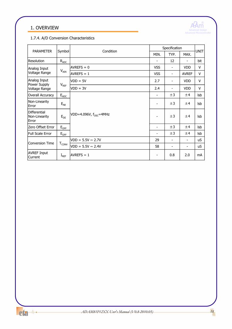
1.7.4. A/D Conversion Characteristics
PARAMETER S b l C di iSpecification
UNITPARAMETER Symbol Condition UNITMIN. TYP. MAX.
Resolution RADC - 12 - bit
Analog InputVoltage Range VAIN
AVREFS = 0 VSS - VDD V
AVREFS = 1 VSS - AVREF V
Analog InputPower SupplyVoltage Range
VREF
VDD = 5V 2.7 - VDD V
VDD = 3V 2 4 VDD VVoltage Range VDD = 3V 2.4 - VDD V
Overall Accuracy EADC
VDD=4.096V, fOSC=4MHz
- ±3 ±4 lsb
Non-LinearityError ENE - ±3 ±4 lsb
DifferentialNon-LinearityError
EDE - ±3 ±4 lsb
Z Off t E E ±3 ±4 l bZero Offset Error EOFF - ±3 ±4 lsb
Full Scale Error EOFF - ±3 ±4 lsb
Conversion Time TCONV
VDD = 5.5V ~ 2.7V 29 - - uS
VDD = 5.5V ~ 2.4V 58 - - uS
AVREF Input Current IREF AVREFS = 1 - 0.8 2.0 mA
18ADAM81P12XX User's Manual (V0.8-2010.05)

ADAm®
Advanced DesignAdvanced Microcontroller
1. OVERVIEW
1.7.5. AC Characteristics (Ta = 25℃)
Parameter Symbol PinSpecification
Unitmin. typ. max.
External clock input cycle time tCP OSC 50 250 1000 ns
External clock input High tCPH OSC 0.5 tCP
External clock input Low tCPL OSC 0.5 tCP
System clock cycle time tSYS 4 tCPSystem clock cycle time tSYS - 4 tCP
External pulse width High tIH EC 1 tCP
External pulse width Low tIL EC 1 tCP
Interrupt pulse width High tIH KS, INT 2 tSYS
Interrupt pulse width Low tIL KS, INT 2 tSYS
RESETB pulse width Low tIL RESETB 8 tSYS
Minimum pulse width
tCP tCPH tCPL
VDD*0 9
OSC
VDD*0.9
VDD*0.1
EC0.8VDD
tIH tIL
KS, INT0.8VDD
0.2VDD
EC0.2VDD
tIH tIL
RESETB0.8VDD
0.2VDD
tIL
19ADAM81P12XX User's Manual (V0.8-2010.05)

ADAm®
Advanced DesignAdvanced Microcontroller
2. FUNCTION DESCRIPTION
2.0. CPU Function Diagram
PG PC
p_AB
d_DB
MU
ProgramMemory Data
Memory
16-level Stackd_AB MG @X
MG @A0 Y
MU
X
X
InstructionRegister
PeripheralRegister
p-DB
r_ABX
GPR (A~H)
#imm
GPR (A~H)
MUXInstructionDecode &Control
ALU
SFR
ControlSignals Program address bus : p_AB
Program data bus : p_DBData address bus : d_ABData bus : d_DBPeripheral address bus : r_AB8-level INTSK
20ADAM81P12XX User's Manual (V0.8-2010.05)
ADAm®
Advanced DesignAdvanced Microcontroller
2. FUNCTION DESCRIPTION
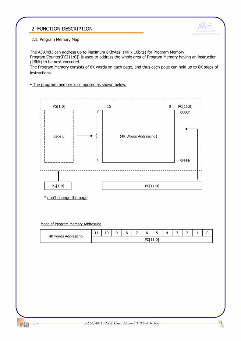
The ADAM81 can address up to Maximum 8Kbytes (4K x 16bits) for Program Memory
2.1. Program Memory Map
The ADAM81 can address up to Maximum 8Kbytes (4K x 16bits) for Program Memory.Program Counter(PC[11:0]) is used to address the whole area of Program Memory having an instruction (16bit) to be next executed.The Program Memory consists of 8K words on each page, and thus each page can hold up to 8K steps of instructions.
• The program memory is composed as shown below.
PG[1:0] 15 0 PC[11:0]
0000h
page 0 (4K Words Addressing)
0FFFh
PG[1:0] PC[11:0]
* don’t change the page.
4K words Addressing11 10 9 8 7 6 5 4 3 2 1 0
PC[11:0]
Mode of Program Memory Addressing
21ADAM81P12XX User's Manual (V0.8-2010.05)

ADAm®
Advanced DesignAdvanced Microcontroller
2. FUNCTION DESCRIPTION
The following registers are used to address the Program Memory.
2.2. Program page Register
• Program page Register (PG) :Holds ROM's page number (page 0 ~ page 3) to be addressed.it is writable by MOVPG instruction Only.
* To change the page,1) MOVPG #pageNo.2) CALL or BR instruction execute.)
S l ti M d f PG
7 6 5 4 3 2 1 0
PG - - PG1 PG0 - - PC14 PC13 79h
initial value 0 0 0 0 0 0 0 0
R/W - - R R - - R R
Selection Mode of PG
Bit Name Selection Mode Remarks
PG[1:0] 00 Program Memory page 0
01 Program Memory page 1
10 Program Memory page 2
11 Program Memory page 3
• Program counter (PC) :Available for addressing word on each page.
This 13-bit binary counter increments for fetching a word to be addressed in the currently dd d h i i t ti t b t t d F i i t
og a e o y page 3
PC14:13] - Program Counter read only
addressed page having an instruction to be next executed. For easier programming, at turning on the power, the program counter is reset to the zero location(0000h). The PGis also set to "0h". Then the program counter specifies the next address. When BR, CALLor RET, RETI instructions are decoded, the switches on each step are turned off not to update the address. Then, for BR or CALL, address data are taken in from the instruction operands (A0 to A11), or for RET, RETI and address including page address is fetched from stack register.
bit 11 0
PC PC
initial value 0000h
Selection Mode of PC
22ADAM81P12XX User's Manual (V0.8-2010.05)
PC[11:0] Program Counter 0000h ~ 0FFFh 4K words Addressing

ADAm®
Advanced DesignAdvanced Microcontroller
2. FUNCTION DESCRIPTION
• Stack Register (SR) :St t d d dd i th b ti ll dStores returned-word address in the subroutine call mode.
The Stack register stores a return address when the subroutine call instruction is executedor interrupt is acknowledged.If subroutine or interrupts are nested to more than 16 levels, internal reset is occurred.The interrupt stack register(INTSK) Saves the contents of Status flag register(SFR) when an interrupt is acknowledged.The Saved contents are restored when an interrupt return(RETI) instruction is executed.INTSK Saves data each time an interrupt is acknowledged but the data stored first is lost
PG[1:0] PC[12:0]
CALL, Interrupt RET, RETI
INTSK Saves data each time an interrupt is acknowledged. but the data stored first is lost if more than 8 levels of interrupts occur.
Stack Register
level 0~
level 15
SFR[3:0]
INTSK
level 0
Interrupt RETI
level 0~
level 7
23ADAM81P12XX User's Manual (V0.8-2010.05)
ADAm®
Advanced DesignAdvanced Microcontroller
2. FUNCTION DESCRIPTION
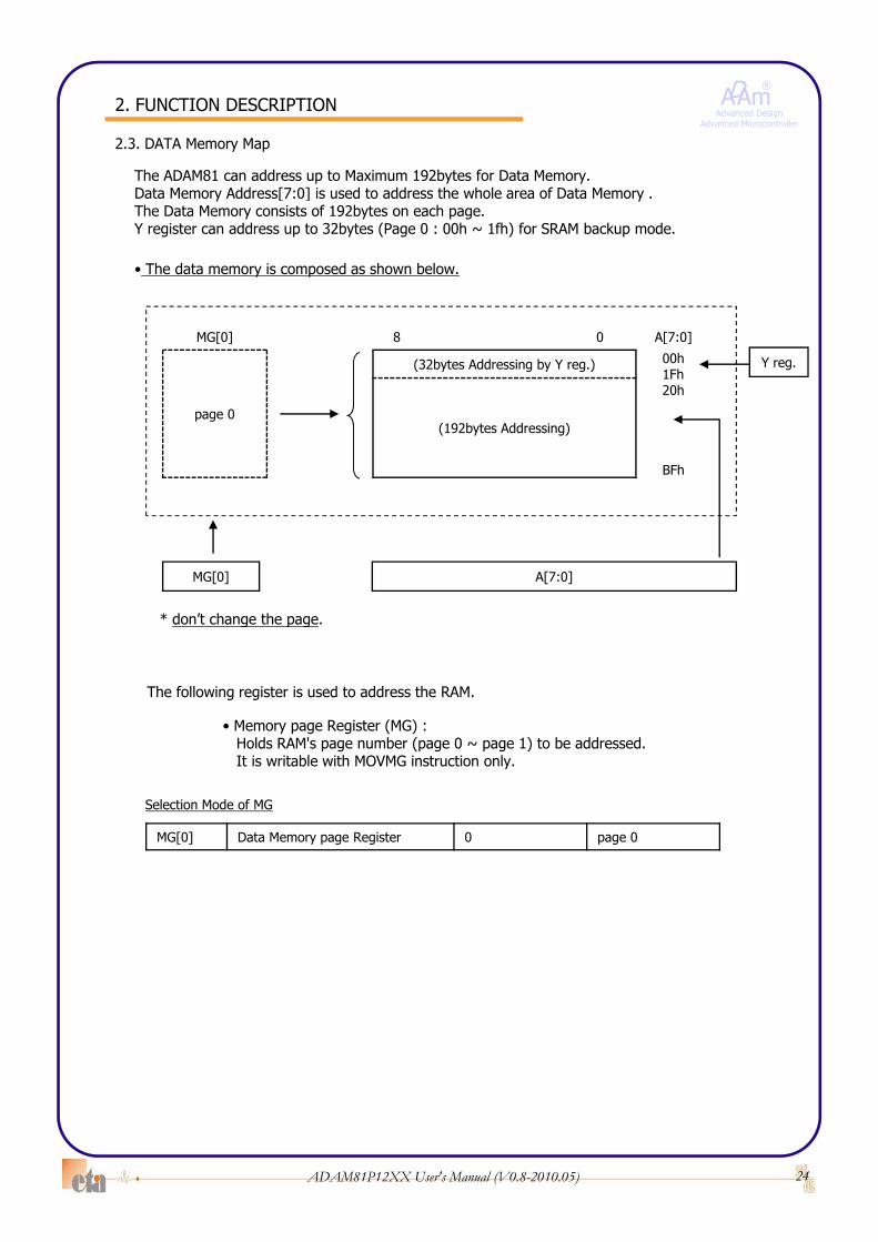
The ADAM81 can address up to Maximum 192bytes for Data Memory.D t M Add [7 0] i d t dd th h l f D t M
2.3. DATA Memory Map
Data Memory Address[7:0] is used to address the whole area of Data Memory .The Data Memory consists of 192bytes on each page.Y register can address up to 32bytes (Page 0 : 00h ~ 1fh) for SRAM backup mode.
• The data memory is composed as shown below.
MG[0] 8 0 A[7 0]MG[0] 8 0 A[7:0]
page 0
(32bytes Addressing by Y reg.) 00h 1Fh20h
BFh
(192bytes Addressing)
Y reg.
MG[0] A[7:0]
* don’t change the page
The following register is used to address the RAM.
• Memory page Register (MG) :Holds RAM's page number (page 0 ~ page 1) to be addressed.It is writable with MOVMG instruction only.
don t change the page.
It is writable with MOVMG instruction only.
Selection Mode of MG
MG[0] Data Memory page Register 0 page 0
24ADAM81P12XX User's Manual (V0.8-2010.05)

ADAm®
Advanced DesignAdvanced Microcontroller
2. FUNCTION DESCRIPTION
The ADAM81 can address up to Maximum 128bytes for Peripheral Control Registers.P i h l Add [6 0] i d t dd th h l f R i t
2.4. Peripheral Memory Map
Peripheral Address[6:0] is used to address the whole area of Registers .
• The Peripheral Register is composed as shown below.
A[6:0] 7 0A[6:0] 7 000h
(128bytes Addressing)
7Fh
A[6:0]
7Fh
25ADAM81P12XX User's Manual (V0.8-2010.05)
ADAm®
Advanced DesignAdvanced Microcontroller
2. FUNCTION DESCRIPTION
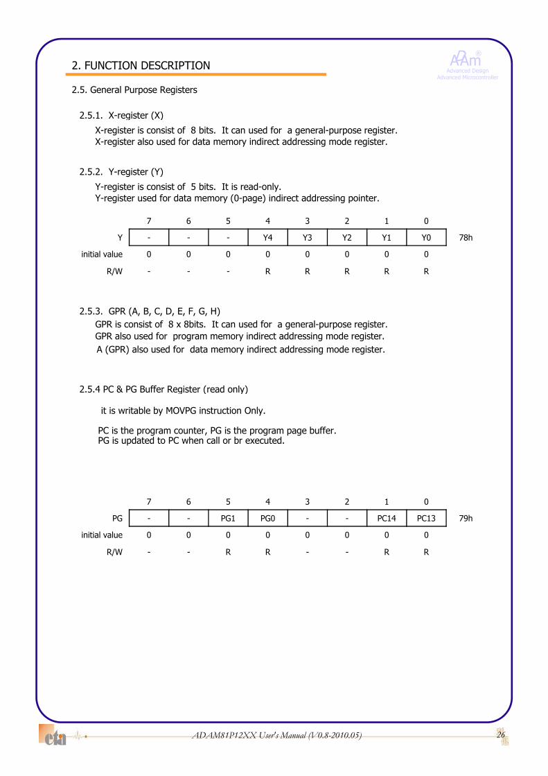
2.5.1. X-register (X)
2.5. General Purpose Registers
2.5.1. X register (X)
X-register is consist of 8 bits. It can used for a general-purpose register.X-register also used for data memory indirect addressing mode register.
2.5.2. Y-register (Y)
Y-register is consist of 5 bits. It is read-only.Y-register used for data memory (0-page) indirect addressing pointer.
7 6 5 4 3 2 1 0
Y - - - Y4 Y3 Y2 Y1 Y0 78h
initial value 0 0 0 0 0 0 0 0
R/W - - - R R R R R
2.5.3. GPR (A, B, C, D, E, F, G, H)GPR is consist of 8 x 8bits. It can used for a general-purpose register.GPR also used for program memory indirect addressing mode register.A (GPR) also used for data memory indirect addressing mode register.
2 5 4 PC & PG Buffer Register (read only)2.5.4 PC & PG Buffer Register (read only)
it is writable by MOVPG instruction Only.
PC is the program counter, PG is the program page buffer.PG is updated to PC when call or br executed.
7 6 5 4 3 2 1 0
PG - - PG1 PG0 - - PC14 PC13 79h
initial value 0 0 0 0 0 0 0 0
R/W - - R R - - R R
26ADAM81P12XX User's Manual (V0.8-2010.05)
ADAm®
Advanced DesignAdvanced Microcontroller
2. FUNCTION DESCRIPTION
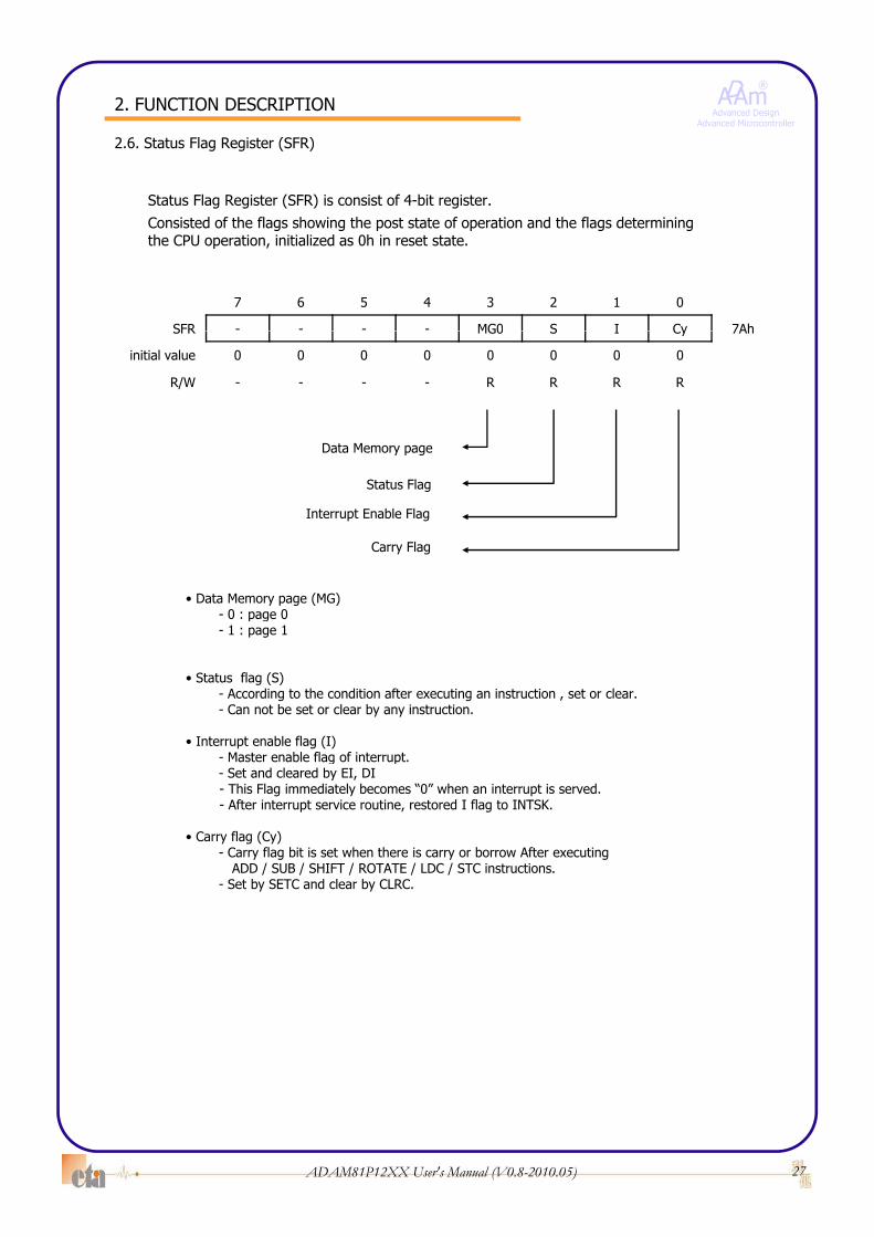
2.6. Status Flag Register (SFR)
Status Flag Register (SFR) is consist of 4-bit register.Consisted of the flags showing the post state of operation and the flags determining the CPU operation, initialized as 0h in reset state.
7 6 5 4 3 2 1 0
SFR - - - - MG0 S I Cy 7AhSFR MG0 S I Cy 7Ah
initial value 0 0 0 0 0 0 0 0
R/W - - - - R R R R
Data Memory page
Carry Flag
Interrupt Enable Flag
Status Flag
• Data Memory page (MG)- 0 : page 00 : page 0 - 1 : page 1
• Status flag (S)- According to the condition after executing an instruction , set or clear. - Can not be set or clear by any instruction.
• Interrupt enable flag (I)- Master enable flag of interrupt.Master enable flag of interrupt.- Set and cleared by EI, DI- This Flag immediately becomes “0” when an interrupt is served.- After interrupt service routine, restored I flag to INTSK.
• Carry flag (Cy)- Carry flag bit is set when there is carry or borrow After executing
ADD / SUB / SHIFT / ROTATE / LDC / STC instructions.- Set by SETC and clear by CLRC.
27ADAM81P12XX User's Manual (V0.8-2010.05)

ADAm®
Advanced DesignAdvanced Microcontroller
2. FUNCTION DESCRIPTION
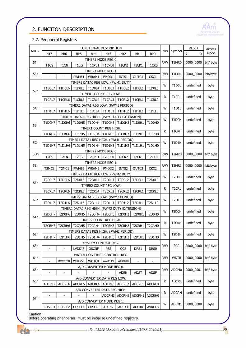
ADDRFUNCTIONAL DESCRIPTION
R/W SymbolRESET Access
2.7. Peripheral Registers
ADDR. R/W Symbol Modebit7 bit6 bit5 bit4 bit3 bit2 bit1 bit0 7 0
00hPORT R0 DATA REG.
R/W R0 1111_1111 *bit/byte- - - - - R02 R01 R00
01hPORT R0 PULL UP SELECTION REG.
W R0PU 1111_1111 byte- - - - - R02PU R01PU R00PU
02hPORT R0 OPEN DRAIN SELECTION REG.
W R0OD 0000_0000 byte- - - - - R02OD R01OD R00OD
03hPORT R0 DIRECTION REG.
R/W R0DD 0000_0000 bit/byte- - - - - R02DD R01DD R00DD
04hPORT R0 FUNCTION SELECTION REG LOW.
R/W R0FL 0000_0000 bit/byte- R02 R01 R00
- - - - - -
08hPORT R1 DATA REG.
R/W R1 1111_1111 *bit/byte- - R15 R14 R13 R12 R11 R10
09hPORT R1 PULL UP SELECTION REG.
W R1PU 1111_1111 byte- - R15PU R14PU R13PU R12PU R11PU R10PU
0AhPORT R1 OPEN DRAIN SELECTION REG.
W R1OD 0000_0000 byte- - R15OD R14OD R13OD R12OD R11OD R10OD
0BhPORT R1 DIRECTION REG.
R/W R1DD 0000_0000 bit/byte- - R15DD R14DD R13DD R12DD R11DD R10DD
0ChPORT R1 FUNCTION SELECTION REG LOW.
R/W R1FL 0000 0000 bit/byte0Ch R/W R1FL 0000_0000 bit/byteR13 R12 R11 R10
0DhPORT R1 FUNCTION SELECTION REG HIGH.
R/W R1FH 0000_0000 bit/byte- - R15 R14
- - - - - -
10hPORT R2 DATA REG.
R/W R2 1111_1111 *bit/byte- - R25 R24 R23 R22 R21 R20
11hPORT R2 PULL UP SELECTION REG.
W R2PU 1111 1111 byte11h W R2PU 1111_1111 byte- - R25PU R24PU R23PU R22PU R21PU R20PU
12hPORT R2 OPEN DRAIN SELECTION REG.
W R2OD 0000_0000 byte- - R25OD R24OD R23OD R22OD R21OD R20OD
13hPORT R2 DIRECTION REG.
R/W R2DD 0000_0000 bit/byte- - R25DD R24DD R23DD R22DD R21DD R20DD
14hPORT R2 FUNCTION SELECTION REG.
R/W R2FN 0000_0000 bit/byte- - R2FN5 R2FN4 R2FN3 R2FN2 R2FN1 R2FN0
- - - - - -
Caution : Before operating pheriperals, Must be initialize undefined registers.*bit is read-modified operation. (SETR1/CLRR1 instruction)
28ADAM81P12XX User's Manual (V0.8-2010.05)

ADAm®
Advanced DesignAdvanced Microcontroller
2. FUNCTION DESCRIPTION
2.7. Peripheral Registers
ADDRFUNCTIONAL DESCRIPTION
R/W SymbolRESET AccessADDR. R/W Symbol Modebit7 bit6 bit5 bit4 bit3 bit2 bit1 bit0 7 0
18hPORT R3 DATA REG.
R/W R3 1111_1111 *bit/byte- - - - - R32 R31 R30
19hPORT R3 PULL UP SELECTION REG.
W R3PU 1111_1111 byte- - - - - R32PU R31PU R30PU
1AhPORT R3 OPEN DRAIN SELECTION REG.
W R3OD 0000_0000 byte- - - - - R32OD R31OD R30OD
1BhPORT R3 DIRECTION REG.
R/W R3DD 0000_0000 bit/byte- - - - - R32DD R31DD R30DD
1ChPORT R3 FUNCTION SELECTION REG.
R/W R3FN 0000_0000 bit/byte- - - - - R3FN2 R3FN1 R3FN0
- - - - - -
40hEXTERNAL INTERRUPT EDGE SELECTION REG 0.
W IEDS0 ----_--00 byte- - - IEDK
41hEXTERNAL INTERRUPT EDGE SELECTION REG 1.
W IEDS1 0000_0000 byte- IED2 IED1 IED0
42hINTERRUPT ENABLE REG 0.
R/W IENR0 0000_0000 bit/byte- - - - INT2E INT1E INT0E KSE
43hINTERRUPT REQUEST FLAG REG 0.
R/W IRQR0 0000_0000 bit/byte- - - - INT2F INT1F INT0F KSF
44hINTERRUPT ENABLE REG 1.
R/W IENR1 0000 0000 bit/byte44h R/W IENR1 0000_0000 bit/byte- VDIE WDTE ADCE - T2E T1E T0E
45hINTERRUPT REQUEST FLAG REG 1.
R/W IRQR1 0000_0000 bit/byte- VDIF WDTF ADCF - T2F T1F T0F
- - - - - -
51hTIMER0 MODE REG 0.
R/W T0MR0 0000_0000 bit/byteT0CS T0CN T0EG T0CPE1 T0CPE0 T0CK2 T0CK1 T0CK0
52hTIMER0 MODE REG 1.
R/W T0MR1 0000 0000 bit/byte52h R/W T0MR1 0000_0000 bit/byteT0MC1 T0MC0 PWME0 WRAM0 FMOD0 INTS0 OUTC0 CKC0
53h
TIMER0 DATA0 REG LOW. (PWM0 DUTY)W T0D0L undefined byte
T0D0L7 T0D0L6 T0D0L5 T0D0L4 T0D0L3 T0D0L2 T0D0L1 T0D0L0
TIMER0 COUNT REG LOW.R T0CRL undefined byte
T0CRL7 T0CRL6 T0CRL5 T0CRL4 T0CRL3 T0CRL2 T0CRL1 T0CRL0
54hTIMER0 DATA1 REG LOW. (PWM0 PERIOD)
W T0D1L undefined byteT0D1L7 T0D1L6 T0D1L5 T0D1L4 T0D1L3 T0D1L2 T0D1L1 T0D1L0
55h
TIMER0 DATA0 REG HIGH. (PWM0 DUTY EXTENSION)W T0D0H undefined byte
T0D0H7 T0D0H6 T0D0H5 T0D0H4 T0D0H3 T0D0H2 T0D0H1 T0D0H0
TIMER0 COUNT REG HIGH.R T0CRH undefined byte
T0CRH7 T0CRH6 T0CRH5 T0CRH4 T0CRH3 T0CRH2 T0CRH1 T0CRH0
56hTIMER0 DATA1 REG HIGH. (PWM0 PERIOD)
W T0D1H undefined byteT0D1H7 T0D1H6 T0D1H5 T0D1H4 T0D1H3 T0D1H2 T0D1H1 T0D1H0
29ADAM81P12XX User's Manual (V0.8-2010.05)
Caution : Before operating pheriperals, Must be initialize undefined registers.*bit is read-modified operation. (SETR1/CLRR1 instruction)
ADAm®
Advanced DesignAdvanced Microcontroller
2. FUNCTION DESCRIPTION
2.7. Peripheral Registers
ADDR.FUNCTIONAL DESCRIPTION
R/W SymbolRESET Access
Modebit7 bit6 bit5 bit4 bit3 bit2 bit1 bit0 7 0 Modebit7 bit6 bit5 bit4 bit3 bit2 bit1 bit0 7 0
57hTIMER1 MODE REG 0.
R/W T1MR0 0000_0000 bit/ byteT1CS T1CN T1EG T1CPE1 T1CPE0 T1CK2 T1CK1 T1CK0
58hTIMER1 MODE REG 1.
R/W T1MR1 0000_0000 bit/byte- - PWME1 WRAM1 FMOD1 INTS1 OUTC1 CKC1
59h
TIMER1 DATA0 REG LOW. (PWM1 DUTY)W T1D0L undefined byte
T1D0L7 T1D0L6 T1D0L5 T1D0L4 T1D0L3 T1D0L2 T1D0L1 T1D0L0
TIMER1 COUNT REG LOWTIMER1 COUNT REG LOW.R T1CRL undefined byte
T1CRL7 T1CRL6 T1CRL5 T1CRL4 T1CRL3 T1CRL2 T1CRL1 T1CRL0
5AhTIMER1 DATA1 REG LOW. (PWM1 PERIOD)
W T1D1L undefined byteT1D1L7 T1D1L6 T1D1L5 T1D1L4 T1D1L3 T1D1L2 T1D1L1 T1D1L0
5Bh
TIMER1 DATA0 REG HIGH. (PWM1 DUTY EXTENSION)W T1D0H undefined byte
T1D0H7 T1D0H6 T1D0H5 T1D0H4 T1D0H3 T1D0H2 T1D0H1 T1D0H0
TIMER1 COUNT REG HIGH.R T1CRH undefined byte
T1CRH7 T1CRH6 T1CRH5 T1CRH4 T1CRH3 T1CRH2 T1CRH1 T1CRH0T1CRH7 T1CRH6 T1CRH5 T1CRH4 T1CRH3 T1CRH2 T1CRH1 T1CRH0
5ChTIMER1 DATA1 REG HIGH. (PWM1 PERIOD)
W T1D1H undefined byteT1D1H7 T1D1H6 T1D1H5 T1D1H4 T1D1H3 T1D1H2 T1D1H1 T1D1H0
5DhTIMER2 MODE REG 0.
R/W T2MR0 0000_0000 bit/ byteT2CS T2CN T2EG T2CPE1 T2CPE0 T2CK2 T2CK1 T2CK0
5EhTIMER2 MODE REG 1.
R/W T2MR1 0000_0000 bit/byteT2MC2 T2MC1 PWME2 WRAM2 FMOD2 INTS2 OUTC2 CKC2
TIMER2 DATA0 REG LOW (PWM2 DUTY)
5Fh
TIMER2 DATA0 REG LOW. (PWM2 DUTY)W T2D0L undefined byte
T2D0L7 T2D0L6 T2D0L5 T2D0L4 T2D0L3 T2D0L2 T2D0L1 T2D0L0
TIMER2 COUNT REG LOW.R T2CRL undefined byte
T2CRL7 T2CRL6 T2CRL5 T2CRL4 T2CRL3 T2CRL2 T2CRL1 T2CRL0
60hTIMER2 DATA1 REG LOW. (PWM2 PERIOD)
W T2D1L undefined byteT2D1L7 T2D1L6 T2D1L5 T2D1L4 T2D1L3 T2D1L2 T2D1L1 T2D1L0
TIMER2 DATA0 REG HIGH. (PWM2 DUTY EXTENSION)W T2D0H undefined byte
T2D0H7 T2D0H6 T2D0H5 T2D0H4 T2D0H3 T2D0H2 T2D0H1 T2D0H061h
T2D0H7 T2D0H6 T2D0H5 T2D0H4 T2D0H3 T2D0H2 T2D0H1 T2D0H0
TIMER2 COUNT REG HIGH.R T2CRH undefined byte
T2CRH7 T2CRH6 T2CRH5 T2CRH4 T2CRH3 T2CRH2 T2CRH1 T2CRH0
62hTIMER2 DATA1 REG HIGH. (PWM2 PERIOD)
W T2D1H undefined byteT2D1H7 T2D1H6 T2D1H5 T2D1H4 T2D1H3 T2D1H2 T2D1H1 T2D1H0
63hSYSTEM CONTROL REG.
R/W SCR 0000_0000 bit/ byte- - LVDDIS OSCNF PSS OCS DRS1 DRS0
WATCH DOG TIMER CONTROL REG64h
WATCH DOG TIMER CONTROL REG.R/W WDTR 0000_0000 bit/ byte
- RCWDTEN WDTRST WDTCK WAKEUP1 WAKEUP0 - -
65hA/D CONVERTER MODE REG 0.
R/W ADCM0 0000_0001 bit/ byte- - - - - ADEN ADST ADSF
66hA/D CONVERTER DATA REG LOW.
R ADCRL undefined byteADCRL7 ADCRL6 ADCRL5 ADCRL4 ADCRL3 ADCRL2 ADCRL1 ADCRL0
A/D CONVERTER DATA REG HIGH.R ADCRH undefined byte
ADCRH3 ADCRH2 ADCRH1 ADCRH0
30ADAM81P12XX User's Manual (V0.8-2010.05)
67h- - - - ADCRH3 ADCRH2 ADCRH1 ADCRH0
A/D CONVERTER MODE REG 1.W ADCM1 0000_0000 byte
CHSEL3 CHSEL2 CHSEL1 CHSEL0 ADCK2 ADCK1 ADCK0 AVREFS
Caution : Before operating pheriperals, Must be initialize undefined registers.
ADAm®
Advanced DesignAdvanced Microcontroller
2. FUNCTION DESCRIPTION
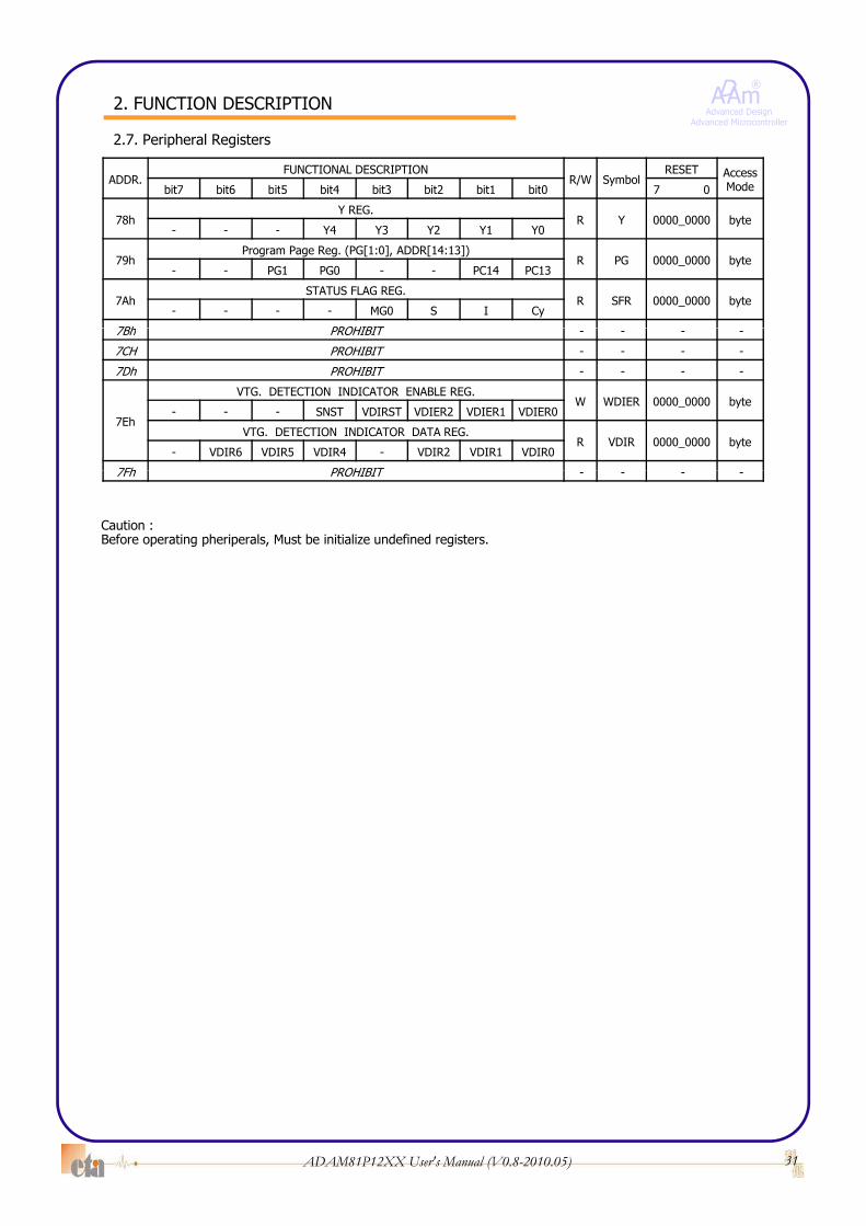
2.7. Peripheral Registers
ADDR.FUNCTIONAL DESCRIPTION
R/W SymbolRESET Access
Modebit7 bit6 bit5 bit4 bit3 bit2 bit1 bit0 7 0 Modebit7 bit6 bit5 bit4 bit3 bit2 bit1 bit0 7 0
78hY REG.
R Y 0000_0000 byte- - - Y4 Y3 Y2 Y1 Y0
79hProgram Page Reg. (PG[1:0], ADDR[14:13])
R PG 0000_0000 byte- - PG1 PG0 - - PC14 PC13
7AhSTATUS FLAG REG.
R SFR 0000_0000 byte- - - - MG0 S I Cy
7Bh PROHIBIT7Bh PROHIBIT - - - -
7CH PROHIBIT - - - -
7Dh PROHIBIT - - - -
7Eh
VTG. DETECTION INDICATOR ENABLE REG.W WDIER 0000_0000 byte
- - - SNST VDIRST VDIER2 VDIER1 VDIER0
VTG. DETECTION INDICATOR DATA REG.R VDIR 0000_0000 byte
- VDIR6 VDIR5 VDIR4 - VDIR2 VDIR1 VDIR0
7Fh PROHIBIT7Fh PROHIBIT - - - -
Caution : Before operating pheriperals, Must be initialize undefined registers.
31ADAM81P12XX User's Manual (V0.8-2010.05)

ADAm®
Advanced DesignAdvanced Microcontroller
3. I/O Ports
The ADAM81 has 18 I/O ports which are R0 (3 I/O), R1 (6 I/O), R2 (6 I/O), R3 (3 I/O).R0 and R1 Port have Stop Release selection register.P ll i t f R0 R1 R2 d R3 t b l t bl bPull-up resistor of R0, R1, R2 and R3 ports can be selectable by program.Pull-down resistor of R30 and R31 ports can be selectable by program. R0, R1, R2 and R3 ports contains data direction register which controls I/O and data register which stores port data.R0, R1, R2 and R3 Ports have Open Drain selection register and Data register.
*R32 is Open Drain output.
Port DataReg.
Pull-upReg.
Open-DrainReg.
DirectionReg.
FunctionReg.
port R0 R0 R0PU R0OD R0DD R0FL
port R1 R1 R1PU R1OD R1DD R1FH/R1FL
port R2 R2 R2PU R2OD R2DD R2FN
I/O Ports Registers
port R2 R2 R2PU R2OD R2DD R2FN
port R3 R3 R3PU R3OD R3DD R3FN
R/W R/W W W R/W R/W
Initial value 1111_1111 1111_1111 0000_0000 0000_0000 0000_0000
default ffh disable enable input disable
32ADAM81P12XX User's Manual (V0.8-2010.05)

ADAm®
Advanced DesignAdvanced Microcontroller
• R0 Data Register (R0)
3. I/O Ports
3.1. Port R0
• R0 Data Register (R0)
R0 data register (R0) is 3-bit register to store data of port R0.
7 6 5 4 3 2 1 0
R0 - - - - - R02 R01 R00 00h
initial value 1 1 1 1 1 1 1 1
R/W - - - - - R/W R/W R/W
• R0 Pull-up Selection Register (R0PU)
g ( ) g pWhen set as the output state by R0DD, and data is written in R0, data is outputted into port R0.When set as the input state, input state of port R0 is readed.bit is read-modified operation. (SETR1/CLRR1 instruction)At output state, if port R0 is readed, R0 is readed instead of port R0.
7 6 5 4 3 2 1 0
R0PU - - - - - R0PU2 R0PU1 R0PU0 01h
R0 pull-up resistor control register (R0PU) is 3-bit register and can control pull-up on or off each bit, if corresponding port is selected as input.If R0PU is selected as “0”, pull-up is enabled and if selected as “1”, it is disabled. The pull-up is automatically disabled, if corresponding port is selected as output.
R0PU R0PU2 R0PU1 R0PU0 01h
initial value 1 1 1 1 1 1 1 1
R/W - - - - - W W W
The pull up is automatically disabled, if corresponding port is selected as output.
• R0 Open Drain Selection Register (R0OD)
7 6 5 4 3 2 1 0
R0OD - - - - - R0OD2 R0OD1 R0OD0 02h
initial value 0 0 0 0 0 0 0 0
R/W W W W
R0 Open Drain Selection Register (R0OD) is 3-bit register, and can assign R0 port as opendrain output port each bit. If R0OD is selected as “0”, port R0 is open drain output, and if selected as “1”, it is push-pull output.
R/W - - - - - W W W
• R0 I/O Data Direction Register (R0DD)
R0 I/O Data Direction Register (R0DD) is 3-bit register, and can assign input state oroutput state to each bit If R0DD is “0” port R0 is in the input state and if “1” it is
/ g ( )
7 6 5 4 3 2 1 0
R0DD - - - - - R0DD2 R0DD1 R0DD0 03h
initial value 0 0 0 0 0 0 0 0
R/W - - - - - R/W R/W R/W
33ADAM81P12XX User's Manual (V0.8-2010.05)
output state to each bit. If R0DD is 0 , port R0 is in the input state, and if 1 , it isin the output state.
ADAm®
Advanced DesignAdvanced Microcontroller
3. I/O Ports
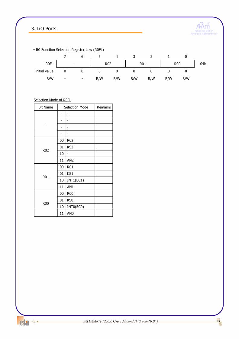
• R0 Function Selection Register Low (R0FL)g ( )
7 6 5 4 3 2 1 0
R0FL - R02 R01 R00 04h
initial value 0 0 0 0 0 0 0 0
R/W - - R/W R/W R/W R/W R/W R/W
Selection Mode of R0FL
Bit Name Selection Mode Remarks
-
- -
- -
- -
- -
R02
00 R02
01 KS2
10 -
11 AN2
00 R01
R0101 KS1
10 INT1(EC1)
11 AN1
R00
00 R00
01 KS0
10 INT0(EC0)( )
11 AN0
34ADAM81P12XX User's Manual (V0.8-2010.05)
ADAm®
Advanced DesignAdvanced Microcontroller
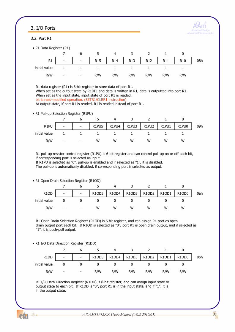
• R1 Data Register (R1)
3. I/O Ports
3.2. Port R1
7 6 5 4 3 2 1 0
R1 - - R15 R14 R13 R12 R11 R10 08h
initial value 1 1 1 1 1 1 1 1
R/W - - R/W R/W R/W R/W R/W R/W
R1 data register (R1) is 6-bit register to store data of port R1.
• R1 Pull-up Selection Register (R1PU)
7 6 5 4 3 2 1 0
R1PU - - R1PU5 R1PU4 R1PU3 R1PU2 R1PU1 R1PU0 09h
When set as the output state by R1DD, and data is written in R1, data is outputted into port R1.When set as the input state, input state of port R1 is readed.bit is read-modified operation. (SETR1/CLRR1 instruction)At output state, if port R1 is readed, R1 is readed instead of port R1.
R1PU R1PU5 R1PU4 R1PU3 R1PU2 R1PU1 R1PU0 09h
initial value 1 1 1 1 1 1 1 1
R/W - - W W W W W W
R1 pull-up resistor control register (R1PU) is 6-bit register and can control pull-up on or off each bit, if corresponding port is selected as input.If R1PU is selected as “0”, pull-up is enabled and if selected as “1”, it is disabled. The p ll p is a tomaticall disabled if co esponding po t is selected as o tp t
• R1 Open Drain Selection Register (R1OD)
7 6 5 4 3 2 1 0
R1OD - - R1OD5 R1OD4 R1OD3 R1OD2 R1OD1 R1OD0 0ah
initial value 0 0 0 0 0 0 0 0
The pull-up is automatically disabled, if corresponding port is selected as output.
R/W - - W W W W W W
R1 Open Drain Selection Register (R1OD) is 6-bit register, and can assign R1 port as opendrain output port each bit. If R1OD is selected as “0”, port R1 is open drain output, and if selected as “1”, it is push-pull output.
R1 I/O Data Direction Register (R1DD)
R1 I/O D t Di e tion Regi te (R1DD) i 6 bit egi te nd n ign inp t t te o
• R1 I/O Data Direction Register (R1DD)
7 6 5 4 3 2 1 0
R1DD - - R1DD5 R1DD4 R1DD3 R1DD2 R1DD1 R1DD0 0bh
initial value 0 0 0 0 0 0 0 0
R/W - - R/W R/W R/W R/W R/W R/W
35ADAM81P12XX User's Manual (V0.8-2010.05)
R1 I/O Data Direction Register (R1DD) is 6-bit register, and can assign input state oroutput state to each bit. If R1DD is “0”, port R1 is in the input state, and if “1”, it isin the output state.

ADAm®
Advanced DesignAdvanced Microcontroller
3. I/O Ports
• R1 Function Selection Register Low (R1FL)g ( )
7 6 5 4 3 2 1 0
R1FL R13 R12 R11 R10 0ch
initial value 0 0 0 0 0 0 0 0
R/W R/W R/W R/W R/W R/W R/W R/W R/W
• R1 Function Selection Register High (R1FH)
Selection Mode of R1FL
7 6 5 4 3 2 1 0
R1FH - - R15 R14 0dh
initial value 0 0 0 0 0 0 0 0
R/W - - - - R/W R/W R/W R/W
Selection Mode of R1FH
Bit Name Selection Mode Remarks
R13
00 R13
01 KS10
10 T0
11 AN10
00 R12
Bit Name Selection Mode Remarks
-
00 -
01 -
10 -
11 -
00 -
R12
00 R12
01 KS9
10 T1
11 AN9
R11
00 R11
01 KS8
10 -
-
00
01 -
10 -
11 -
R15
00 R15
01 KS12
10 CLO10 -
11 AN8
R10
00 R10
01 KS7
10 INT2(EC2)
11 AN7
10 CLO
11 AN12
R14
00 R14
01 KS11
10 -
11 AN11
36ADAM81P12XX User's Manual (V0.8-2010.05)

ADAm®
Advanced DesignAdvanced Microcontroller
• R2 Data Register (R2)
3. I/O Ports
3.3. Port R2
7 6 5 4 3 2 1 0
R2 - - R25 R24 R23 R22 R21 R20 10h
initial value 1 1 1 1 1 1 1 1
R/W - - R/W R/W R/W R/W R/W R/W
R2 data register (R2) is 6-bit register to store data of port R2.
• R2 Pull-up Selection Register (R2PU)
7 6 5 4 3 2 1 0
g ( ) g pWhen set as the output state by R2DD, and data is written in R2, data is outputted into port R2.When set as the input state, input state of port R2 is readed.bit is read-modified operation. (SETR1/CLRR1 instruction)At output state, if port R2 is readed, R2 is readed instead of port R2.
R2PU - - R2PU5 R2PU4 R2PU3 R2PU2 R2PU1 R2PU0 11h
initial value 1 1 1 1 1 1 1 1
R/W - - W W W W W W
R2 pull-up resistor control register (R2PU) is 6-bit register and can control pull-up on or off each bit, if corresponding port is selected as input.If R2PU is selected as “0”, pull-up is enabled and if selected as “1”, it is disabled.
• R2 Open Drain Selection Register (R2OD)
7 6 5 4 3 2 1 0
R2OD - - R2OD5 R2OD4 R2OD3 R2OD2 R2OD1 R2OD0 12h
initial value 0 0 0 0 0 0 0 0
, p p ,The pull-up is automatically disabled, if corresponding port is selected as output.
R/W - - W W W W W W
• R2 I/O Data Direction Register (R2DD)
R2 Open Drain Selection Register (R2OD) is 6-bit register, and can assign R2 port as opendrain output port each bit. If R2OD is selected as “0”, port R2 is open drain output, and if selected as “1”, it is push-pull output.
R2 I/O Data Direction Register (R2DD) is 6-bit register, and can assign input state or
7 6 5 4 3 2 1 0
R2DD - - R2DD5 R2DD4 R2DD3 R2DD2 R2DD1 R2DD0 13h
initial value 0 0 0 0 0 0 0 0
R/W - - R/W R/W R/W R/W R/W R/W
37ADAM81P12XX User's Manual (V0.8-2010.05)
output state to each bit. If R2DD is “0”, port R2 is in the input state, and if “1”, it isin the output state.

ADAm®
Advanced DesignAdvanced Microcontroller
3. I/O Ports
• R2 Function selection Register (R2FN)g ( )
7 6 5 4 3 2 1 0
R2FN - - R2FN5 R2FN4 R2FN3 R2FN2 R2FN1 R2FN0 14h
initial value 0 0 0 0 0 0 0 0
R/W - - R/W R/W R/W R/W R/W R/W
Selection Mode of R2FN
Bit Name Selection Mode Remarks
-0 -
1 -
-0 -
1 -
R2FN50 R25
1 AN15
R2FN40 R24
1 AN14
R2FN30 R23
1 AN13
R2FN20 R22
1 TM01
R2FN10 R21
1 TM12
R2FN00 R20
1 T2
38ADAM81P12XX User's Manual (V0.8-2010.05)

ADAm®
Advanced DesignAdvanced Microcontroller
• R3 Data Register (R3)
3. I/O Ports
3.4. Port R3
7 6 5 4 3 2 1 0
R3 - - - - - R32 R31 R30 18h
initial value 1 1 1 1 1 1 1 1
R/W - - - - - R/W R/W R/W
R3 data register (R3) is 3-bit register to store data of port R3.When set as the output state by R3DD and data is written in R3 data is outputted into port R3
• R3 Pull-up Selection Register (R3PU)
7 6 5 4 3 2 1 0
R3PU - - - - - R3PU2 R3PU1 R3PU0 19h
When set as the output state by R3DD, and data is written in R3, data is outputted into port R3.When set as the input state, input state of port R3 is readed.bit is read-modified operation. (SETR1/CLRR1 instruction)At output state, if port R3 is readed, R3 is readed instead of port R3.
initial value 1 1 1 1 1 1 1 1
R/W - - - - - W W W
R3 pull-up resistor control register (R3PU) is 3-bit register and can control pull-up on or off each bit, if corresponding port is selected as input.If R3PU is selected as “0”, pull-up is enabled and if selected as “1”, it is disabled. The pull-up is automatically disabled, if corresponding port is selected as output.
• R3 Open Drain Selection Register (R3OD)
7 6 5 4 3 2 1 0
R3OD - - - - - R3OD2 R3OD1 R3OD0 1ah
initial value 0 0 0 0 0 0 0 0
R/W W W W
p p y , p g p p
R/W - - - - - W W W
• R3 I/O Data Direction Register (R3DD)
7 6 5 4 3 2 1 0
R3 Open Drain Selection Register (R3OD) is 3-bit register, and can assign R3 port as opendrain output port each bit. If R3OD is selected as “0”, port R3 is open drain output, and if selected as “1”, it is push-pull output.
R3 I/O Data Direction Register (R3DD) is 3-bit register, and can assign input state oroutput state to each bit. If R3DD is “0”, port R3 is in the input state, and if “1”, it isin the output state
7 6 5 4 3 2 1 0
R3DD - - - - - R3DD2 R3DD1 R3DD0 1bh
initial value 0 0 0 0 0 0 0 0
R/W - - - - - R/W R/W R/W
39ADAM81P12XX User's Manual (V0.8-2010.05)
in the output state.
ADAm®
Advanced DesignAdvanced Microcontroller
3. I/O Ports
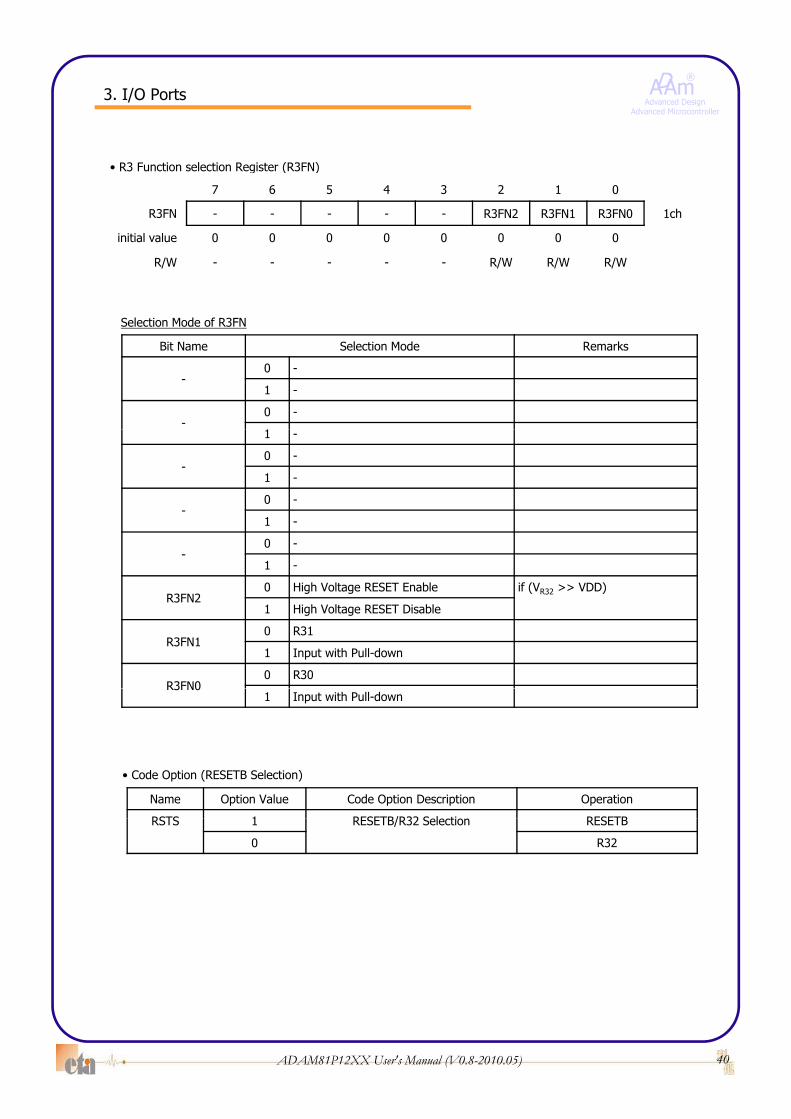
• R3 Function selection Register (R3FN)R3 Function selection Register (R3FN)
7 6 5 4 3 2 1 0
R3FN - - - - - R3FN2 R3FN1 R3FN0 1ch
initial value 0 0 0 0 0 0 0 0
R/W - - - - - R/W R/W R/W
Selection Mode of R3FN
Bit Name Selection Mode Remarks
-0 -
1 -
-0 -
1 -
-0 -
1 -
-0 -
1 -
-0 -
1 -
R3FN20 High Voltage RESET Enable if (VR32 >> VDD)
1 High Voltage RESET Disable
R3FN10 R31
1 Input with Pull-down
R3FN00 R30
R3FN01 Input with Pull-down
• Code Option (RESETB Selection)
Name Option Value Code Option Description Operation
RSTS 1 RESETB/R32 S l ti RESETBRSTS 1 RESETB/R32 Selection RESETB
0 R32
40ADAM81P12XX User's Manual (V0.8-2010.05)

ADAm®
Advanced DesignAdvanced Microcontroller
4. Oscillation Circuit
4.1. Oscillation Circuit
Oscillation circuit is designed to be used either with a ceramic resonator or crystal oscillator.Fi 4 1 h i it di i t l ( i ) ill t d t l l kFig. 4.1 shows circuit diagrams using a crystal (or ceramic) oscillator and external clock.Clock from oscillation circuit makes CPU clock via clock pulse generator, and then provide peripheral hardware clock.Alternately, the oscillator may be driven from an external source as shown is Fig. 4.1.In the STOP mode, oscillation stop, OSC2 state goes to “High”, OSC1 state goes to “Low”, and built-in feed back resistor is disabled.
Fig Pin Assignments of Oscillator configurationFig. Pin Assignments of Oscillator configuration
External Crystal (Ceramic) oscillator circuitExternal clock input circuit
External clock
COSC1OSC1
C
External R circuit Internal oscillator circuit
OSC2R31
R
InternalOscillator
R31
OSC1
R31
R30
Name XTS[2:0] SXT Code Option Description R30 Assign R31 Assign
111 1 Internal RC 4MHz R30(I/O) R31(I/O)
110 1 Internal RC 2MHz R30(I/O) R31(I/O)
• Code Option (Oscillator Selection)
XTS
101 1 Internal RC 1MHz R30(I/O) R31(I/O)
100 1 Internal RC 8MHz R30(I/O) R31(I/O)
011 1 Internal RC 16MHz R30(I/O) R31(I/O)
010 1 XT Oscillator OSC1(I) OSC2(O)
001 1 External Clock Input OSC1(I) R31(I/O)
000 1 External RC Oscillator OSC1(I) R31(I/O)
41ADAM81P12XX User's Manual (V0.8-2010.05)
( ) ( / )
SXT 010 0 32.768KHz Oscillator OSC1(I) OSC2(O)

ADAm®
Advanced DesignAdvanced Microcontroller
4. Oscillation Circuit
4.2. System Clock & Peripheral Clock Generator Block Diagram
System Clock(Tck = 4/fOSC)
CodeOption
Internal RCOSC16/8/4/2/1 (MHz)
External Crystal/Oscillator
External
111~
011
010
DRS
1/2
1/8
1/16
Clock Divider
MUX
00
01
10
11 PSS
sfOSC fOSC
External R-OSC
ExternalClock Input 001
000
RCWDT
Peripheral Clock(PS0)
MUX01
R15
1/16 11 PSS
MUX01
OCSRCWDTEN CLO
42ADAM81P12XX User's Manual (V0.8-2010.05)

ADAm®
Advanced DesignAdvanced Microcontroller
4. Oscillation Circuit
• System Control Register
7 6 5 4 3 2 1 0
SCR - - LVDDIS OSCNF PSS OCS DRS1 DRS0 63h
initial value 0 0 0 0 0 0 0 0
R/W - - R/W R/W R/W R/W R/W R/W
Selection Mode of SCR
Bit Name Selection Mode Remarks
LVDDIS LVD Disable0 Enable *1 Disable
OSCNF OSC. Noise Filter Enable0 Disable *1 Enable
PSS Peripheral Clock Selection0 fOSC to PS0 *1 sfOSC to PS00 f O t t
OCS Output Clock Selection0 sfOSC Output1 RCWDT Output
DRS[1:0] Divide Ratio Selection
00 sfOSC
fOSC01 sfOSC/210 sfOSC/811 sfOSC/16
43ADAM81P12XX User's Manual (V0.8-2010.05)

ADAm®
Advanced DesignAdvanced Microcontroller
4. Oscillation Circuit
• Selection of Peripheral Clock
PeripheralClock Source
PSS=0 PSS=1 RemarksDRS=0
(fOSC=sfOSC)DRS=1
(fOSC=sfOSC/2)DRS=2
(fOSC=sfOSC/8)DRS=3
(fOSC=sfOSC/16)DRS=x
(fOSC=sfOSC)PS0 fOSC fOSC/2 fOSC/8 fOSC/16 fOSCPS1 fOSC/2 fOSC/4 fOSC/16 fOSC/32 fOSC/2PS2 fOSC/4 fOSC/8 fOSC/32 fOSC/64 fOSC/4PS3 fOSC/8 fOSC/16 fOSC/64 fOSC/128 fOSC/8PS4 fOSC/16 fOSC/32 fOSC/128 fOSC/256 fOSC/16PS4 fOSC/16 fOSC/32 fOSC/128 fOSC/256 fOSC/16PS5 fOSC/32 fOSC/64 fOSC/256 fOSC/512 fOSC/32PS6 fOSC/64 fOSC/128 fOSC/512 fOSC/1024 fOSC/64PS7 fOSC/128 fOSC/256 fOSC/1024 fOSC/2048 fOSC/128PS8 fOSC/256 fOSC/512 fOSC/2048 fOSC/4096 fOSC/256
4.2.2. fOSC Change Method
fOSC
sfOSC
DRS(01) 1/2 DRS(00)
fOSC
1/8
DRS(10)
ClockDivider
System Clock(Tck 4/f )
DRS(00)
DRS(00) DRS(11)1/16
Divider (Tck = 4/fOSC)
fOSC
44ADAM81P12XX User's Manual (V0.8-2010.05)
ADAm®
Advanced DesignAdvanced Microcontroller
5. Watch Dog Timer
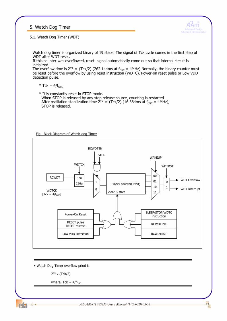
5.1. Watch Dog Timer (WDT)
Watch dog timer is organized binary of 19 steps. The signal of Tck cycle comes in the first step of WDT after WDT reset.If this counter was overflowed, reset signal automatically come out so that internal circuit is initialized.The overflow time is 219 × (Tck/2) (262.144ms at fOSC = 4MHz) Normally, the binary counter must be reset before the overflow by using reset instruction (WDTC), Power-on reset pulse or Low VDD detection pulse.
* Tck = 4/fOSC Tck = 4/fOSC
* It is constantly reset in STOP mode.When STOP is released by any stop release source, counting is restarted.After oscillation stabilization time 215 × (Tck/2) [16.384ms at fOSC = 4MHz], STOP is released.
Fig. Block Diagram of Watch-dog Timer
STOP
RCWDTEN
WAKEUP
Binary counter(19bit)
WDTCK[Tck = 4/fOSC]
clear & start
0
1
32u
256u
WDTCK
00
01
10
11
WDT Overflow
WDT Interrupt
1
0
RCWDT
WDTRST
Power-On Reset
RESET pulseRESET release
Low VDD Detection
RCWDTINT
SLEEP/STOP/WDTCinstruction
RCWDTRSTLow VDD Detection RCWDTRST
• Watch Dog Timer overflow priod is
45ADAM81P12XX User's Manual (V0.8-2010.05)
219 x (Tck/2)
where, Tck = 4/fOSC
ADAm®
Advanced DesignAdvanced Microcontroller
5. Watch Dog Timer
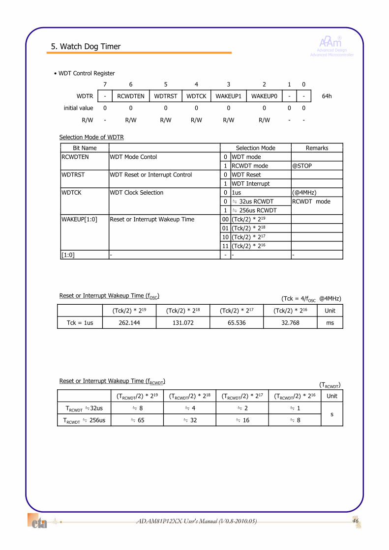
• WDT Control Register
7 6 5 4 3 2 1 07 6 5 4 3 2 1 0
WDTR - RCWDTEN WDTRST WDTCK WAKEUP1 WAKEUP0 - - 64h
initial value 0 0 0 0 0 0 0 0
R/W - R/W R/W R/W R/W R/W - -
Selection Mode of WDTR
Bit Name Selection Mode RemarksBit Name Selection Mode RemarksRCWDTEN WDT Mode Contol 0 WDT mode
1 RCWDT mode @STOPWDTRST WDT Reset or Interrupt Control 0 WDT Reset
1 WDT InterruptWDTCK WDT Clock Selection 0 1us (@4MHz)
0 ≒ 32us RCWDT RCWDT mode1 ≒ 256us RCWDT1 ≒ 256us RCWDT
WAKEUP[1:0] Reset or Interrupt Wakeup Time 00 (Tck/2) * 219
01 (Tck/2) * 218
10 (Tck/2) * 217
11 (Tck/2) * 216
[1:0] - - - -
(Tck/2) * 219 (Tck/2) * 218 (Tck/2) * 217 (Tck/2) * 216 Unit
Tck = 1us 262.144 131.072 65.536 32.768 ms
Reset or Interrupt Wakeup Time (fOSC) (Tck = 4/fOSC @4MHz)
(TRCWDT/2) * 219 (TRCWDT/2) * 218 (TRCWDT/2) * 217 (TRCWDT/2) * 216 Unit
Reset or Interrupt Wakeup Time (fRCWDT) (TRCWDT)
TRCWDT ≒32us ≒ 8 ≒ 4 ≒ 2 ≒ 1s
TRCWDT ≒ 256us ≒ 65 ≒ 32 ≒ 16 ≒ 8
46ADAM81P12XX User's Manual (V0.8-2010.05)
ADAm®
Advanced DesignAdvanced Microcontroller
5. Watch Dog Timer
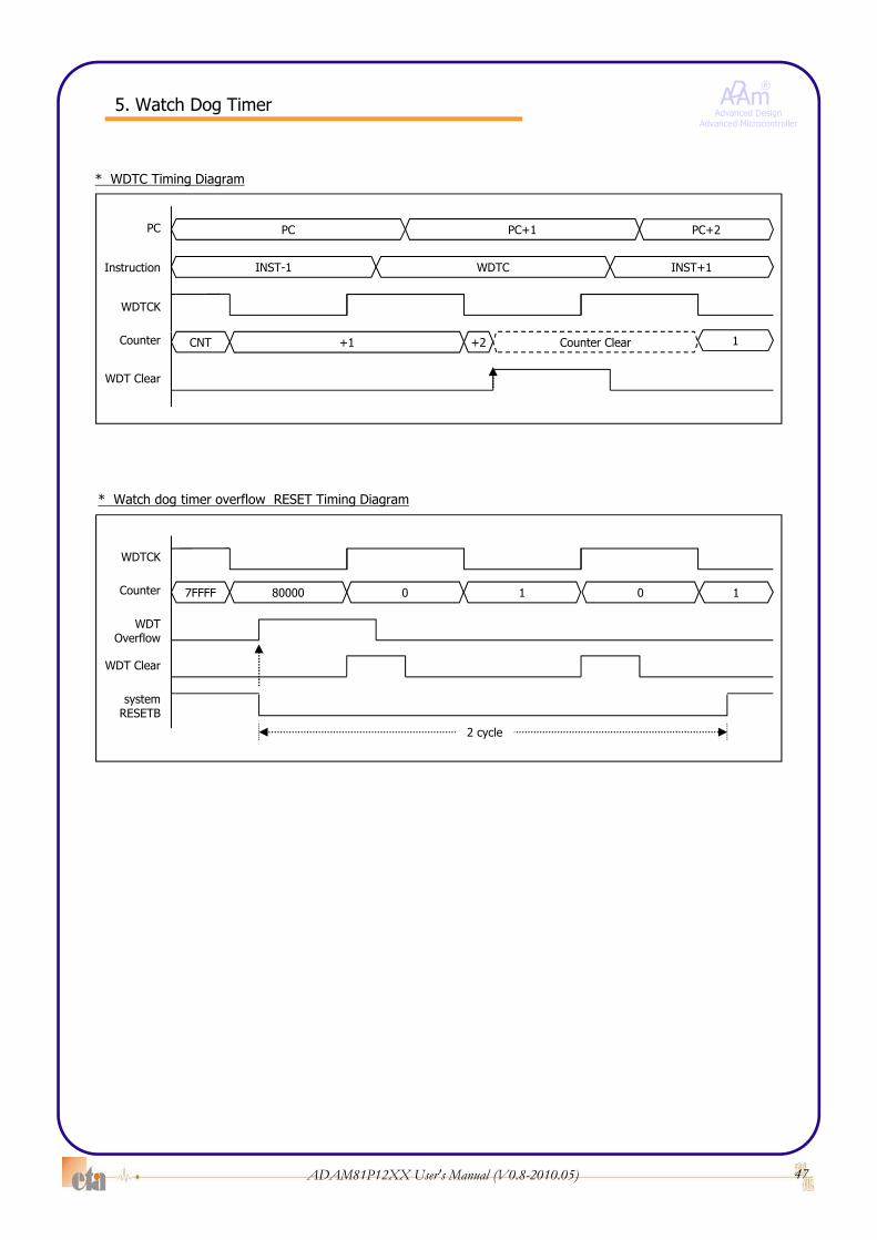
* WDTC Timing Diagram
PC
Instruction
WDTCK
PC PC+1 PC+2
INST-1 WDTC INST+1
WDT Clear
+1CNTCounter +2 Counter Clear 1
* Watch dog timer overflow RESET Timing Diagram
WDTCK
800007FFFFCounter 0 1 0 1
WDT Clear
WDTOverflow
systemRESETB
2 cycle
47ADAM81P12XX User's Manual (V0.8-2010.05)

ADAm®
Advanced DesignAdvanced Microcontroller
6. Timer
6.1. Timer
6 1 1 Ti i d6.1.1. Timer operation mode
Timer is basically made of Timer Data/Counter Register, Timer Mode Register and control circuit.The types of Timer are 16bit Timer/Counter (Timer0, Timer1, Timer2).
Timer0
-. 16-bit Interval Timer-. 16-bit Event Counter
16 bit C t TiTimer0 -. 16-bit Capture Timer-. 16-bit rectangular-wave output
Timer1
-. 16-bit Interval Timer-. 16-bit Event Counter-. 16-bit Capture Timer-. 16-bit rectangular-wave output
Timer2
-. 16-bit Interval Timer-. 16-bit Event CounterTimer2 -. 16-bit Capture Timer-. 16-bit rectangular-wave output
48ADAM81P12XX User's Manual (V0.8-2010.05)

ADAm®
Advanced DesignAdvanced Microcontroller
6. Timer
6.2. Timer0
6.2.1. Timer0(T0) Block Diagram( ) g
TIMER0 DATA1BUFFER
TIMER0 DATA0BUFFER
MOVR H,T0CRHMOVR G,T0CRL
MOVR T0D1H,#AAHMOVR T0D1L,#55H
MOVR T0D0H,#55HMOVR T0D0L,#AAH
SRAM(@Y)
T0MR0
TIMER0 DATA1REGISTER
(T0D1H:T0D1L)
TIMER0 DATA0REGISTER
(T0D0H:T0D0L)
BUFFER(T0D1H:T0D1L)
BUFFER(T0D0H:T0D0L)
T0 load
EG CPECS CN TCK
TIMER0 COUNTREG. (T0CRH:T0CRL)
WRAM & capture
(@Y)
7 6 5 4 3 2 1 0
TCK
T0 (16-bit)Counter &
01234567
1 0MUX
PS1PS2PS3PS4PS5T1T2EC
01234
PS0/2PS0PS6PS7PS8
FMODCKC
01 ** Every 2’nd Counter Overflow
** Every Counter Overflow(capture mode)
T0FINT.GEN.
CS T0 load
OUTPUT
Comparator
T0
10
11
EC0/INT0 Edge det.
EC1/INT1 Edge det.
0001 CPE
capture & clear
CPE+0+1
EG
CKC
INTS
0GEN. T0Note> The status of T0 Output is “0” for counting T0D0H:T0D0L
also, “1” for counting T0D1H:T0D1L.R1FL
TMCPWME
WRAMFMOD
INTSOUTC
CKC
OUTC
01
T0MR1
7 6 5 4 3 2 1 0
49ADAM81P12XX User's Manual (V0.8-2010.05)

ADAm®
Advanced DesignAdvanced Microcontroller
6. Timer
6.2.2. Timer0 Control Register
• Timer0 Mode Register 0 (T0MR0)
7 6 5 4 3 2 1 0
T0MR0 T0CS T0CN T0EG T0CPE1 T0CPE0 T0CK2 T0CK1 T0CK0 51h
initial value 0 0 0 0 0 0 0 0
R/W R/W R/W R/W R/W R/W R/W R/W R/W
g
R/W R/W R/W R/W R/W R/W R/W R/W R/W
Selection Mode of T0MR0
Bit Name Selection Mode Remarks
T0CS Timer0 Clear / start Control0 Timer0 Stop
1 Timer0 Clear and Start
0 Time 0 P e
(fOSC = 4MHz)
T0CN Timer0 Pause / Continue Control0 Timer0 Pause
1 Timer0 continue
T0EG Timer0 Count Control0 Timer0 Count
1 Timer0 Count + 1
T0CPE1T0CPE0
Input capture &Event Count selection
00 EC0
01 EC1
10 C 0 (INT0)T0CPE0 Event Count selection 10 Capture 0 (INT0)
11 Capture 1 (INT1)
T0CK2T0CK1 Input clock selection
000 PS1 (0.5us) *PS0/2 *FMODE
001 PS2 (1us) *PS0 (0.25us)
010 PS3 (2us) *PS6 (16us)
011 PS4 (4us) *PS7 (32us)
T0CK0p
100 PS5 (8us) *PS8 (64us)
101 T1
110 T2
111 EC (EC0 or EC1)
50ADAM81P12XX User's Manual (V0.8-2010.05)

ADAm®
Advanced DesignAdvanced Microcontroller
6. Timer
• Timer0 Mode Register 1 (T0MR1)
7 6 5 4 3 2 1 07 6 5 4 3 2 1 0
T0MR1 T0MC1 T0MC0 PWME0 WRAM0 FMOD0 INTS0 OUTC0 CKC0 52h
initial value 0 0 0 0 0 0 0 0
R/W R/W R/W R/W R/W R/W R/W R/W R/W
Selection Mode of T0MR1
Bit Name Selection Mode Remarks
T0MC1T0MC0 mPWM Control
00 Logical ‘AND’ of Timer0 output and Timer1 output
01 Logical ‘OR’ of Timer0 output and Timer1 output
10 Logical ‘NAND’ of Timer0 output and Timer1 output
11 Logical ‘NOR’ of Timer0 output and Timer1 output
PWME0 Ti /PWM M d S l ti0 Timer0 Normal Mode
PWME0 Timer/PWM Mode Selection1 Timer0 PWM Mode
WRAM0 Automatically Save Capture data to RAM0 Disable
1 Timer0 Automatically Save Capture data to RAM
FMOD0 Fast Mode Selection0 Timer0 Normal Mode
1 Timer0 Fast Mode
0 Timer0 Interrupt Every 2nd OverflowINTS0 Timer0 Interrupt Overflow Control
p y
1 Timer0 Interrupt Every Overflow
OUTC0 Timer0 Output Control0 Timer0 Output Normal
1 Timer0 Output Reverse
CKC0 Timer0 Input Clock Control0 Timer0 Input Clock Normal
1 Timer0 Input Clock Reverse
N t S 2b t t d t t RAM (2 l ) dd d b @Y T0CRL d fi tNote: Save 2bytes capture data to RAM (2cycle) - addressed by @Y++., T0CRL saved first.
0 1 2 3 4 5 6 7SRAM(@Y)
T0CRL T0CRH T0CRL T0CRH T0CRL T0CRH T0CRL T0CRH
1’st Captured Data 2’nd Captured Data 3’rd Captured Data 4’th Captured Data
51ADAM81P12XX User's Manual (V0.8-2010.05)
ADAm®
Advanced DesignAdvanced Microcontroller
6. Timer
• Timer0 Data0 Register Low (T0D0L) = PWM0 DUTY
7 6 5 4 3 2 1 07 6 5 4 3 2 1 0
T0D0L T0D0L7 T0D0L6 T0D0L5 T0D0L4 T0D0L3 T0D0L2 T0D0L1 T0D0L0 53h
initial value - - - - - - - -
R/W W W W W W W W W
• Timer0 Count Register Low (T0CRL)
7 6 5 4 3 2 1 0
T0CRL T0CRL7 T0CRL6 T0CRL5 T0CRL4 T0CRL3 T0CRL2 T0CRL1 T0CRL0 53h
initial value - - - - - - - -
R/W R R R R R R R RR/W R R R R R R R R
• Timer0 Data1 Register Low (T0D1L) = PWM0 PERIOD
Note: At 16bit counter value read, Must be read T0CRL first.
Timer0 Data1 Register Low (T0D1L) PWM0 PERIOD
7 6 5 4 3 2 1 0
T0D1L T0D1L7 T0D1L6 T0D1L5 T0D1L4 T0D1L3 T0D1L2 T0D1L1 T0D1L0 54h
initial value - - - - - - - -
R/W W W W W W W W W
52ADAM81P12XX User's Manual (V0.8-2010.05)
ADAm®
Advanced DesignAdvanced Microcontroller
6. Timer
• Timer0 Data0 Register High (T0D0H) = PWM0 DUTY EXTENSION
7 6 5 4 3 2 1 07 6 5 4 3 2 1 0
T0D0H T0D0H7 T0D0H6 T0D0H5 T0D0H4 T0D0H3 T0D0H2 T0D0H1 T0D0H0 55h
initial value - - - - - - - -
R/W W W W W W W W W
• Timer0 Count Register High (T0CRH)
7 6 5 4 3 2 1 0
T0CRH T0CRH7 T0CRH6 T0CRH5 T0CRH4 T0CRH3 T0CRH2 T0CRH1 T0CRH0 55h
initial value - - - - - - - -
R/W R R R R R R R RR/W R R R R R R R R
• Timer0 Data1 Register High (T0D1H) = PWM0 CYCLE
7 6 5 4 3 2 1 0
Note: At 16bit counter value read, Must be read T0CRL first.
7 6 5 4 3 2 1 0
T0D1H T0D1H7 T0D1H6 T0D1H5 T0D1H4 T0D1H3 T0D1H2 T0D1H1 T0D1H0 56h
initial value - - - - - - - -
R/W W W W W W W W W
53ADAM81P12XX User's Manual (V0.8-2010.05)

ADAm®
Advanced DesignAdvanced Microcontroller
6. Timer
6.2.3. Timer0 Caution
TCK
T0CS (Clear & Start, move data from buffer to reg.)
Caution : In the case of T0EG is “0”,
T0F(regardless of TCK)
T0
T0D1H/T0D1L
T0D0H/T0D0L
0Counter
0000h
0000h
0000h
0001h
0001h
0000h
1 0 1 0 1 0 1 0 1 0 1 0 1 0 1 0 1 0 1 0 1
T0(regardless of TCK)
hold before status
Want to count “0”, set T0EG=1
54ADAM81P12XX User's Manual (V0.8-2010.05)

ADAm®
Advanced DesignAdvanced Microcontroller
6. Timer
6.2.4. TM01 Mode
* TM01 Logical Output Control
T0
T1TMC[1:0]
00
01
10
11
TM01
* TM01 mode Timing Diagram
T0
TMC
TM01 mode Timing Diagram
0 (AND)
T1
1 (OR) 2 (NAND) 3 (NOR)
TM01
55ADAM81P12XX User's Manual (V0.8-2010.05)

ADAm®
Advanced DesignAdvanced Microcontroller
6. Timer
* 16 bit Timer/Counter mode Timing Diagram
6.2.5. Timer0 Timing Diagram
* 16-bit Timer/Counter mode Timing Diagram
T0CS
T0D0H:T0D0L
TCK
T0CN
FFFFhT0D1H:T0D1L
T0D0H T0D0L
CS &Reload
T0Counter
0000hCS &Reload
CS &Reload
CS &Reload
T0D0H:T0D0L
Reload
Interval period
T0F
T0
Interval period
Reload Reload Reload
T0F(INTS0=1)
Note > CS : Timer0 Counter Clear & Start.Reload : Timer0 Data move from Data buffer to Data register.
* Start / Stop operation
(INTS0 1)
T0Counter
TCK
FFFFh
T0D0H:T0D0L T0D0H:T0D0L T0D0H:T0D0L
T0D1H:T0D1L
Counter
0000h
Pause
continue
T0CS
Stop Pause
continue
56ADAM81P12XX User's Manual (V0.8-2010.05)
T0CN

ADAm®
Advanced DesignAdvanced Microcontroller
6. Timer
T0CS (Clear & Start, move data from buffer to reg.)
* 16-bit Timer/Counter mode Timing Diagram
TCK
m qT0D1H:T0D1L
n pT0D0H:T0D0L
( g )
0
0
T0F (Clear & Start, move data from buffer to reg.)
T0F
T0
0 1 ~ 0 ~Counter n 0mn-1 m-1 1 ~ 0 ~p 0qp-1 q-1 1
clear clear
T0F(INTS0=1)
TCK
T0CS (Clear & Start, move data from buffer to reg.)
* 16-bit Capture mode Timing Diagram
TCK
T0D1H:T0D1L
T0D0H:T0D0L
0 1 ~ 0 1Counter 3 32 2 4 ~ 0 1FF 02FE 2
clear
-
T0F
1
match
don’t care --
00FFh -
INT0F or INT1F(rising edge)
INT0 or INT1
clear
T0CRH - 00 00
capture capture
T0CRL - 03 02
1’st Interrupt interval period= 03h
2’nd Interrupt interval period= FFh + 02h
capture capture
T0CRL T0CRH T0CRL T0CRH
WT(WRAM0=1)
57ADAM81P12XX User's Manual (V0.8-2010.05)
T0CRL
00 0201
T0CRH T0CRL T0CRH
03@Y
ADAm®
Advanced DesignAdvanced Microcontroller
6. Timer
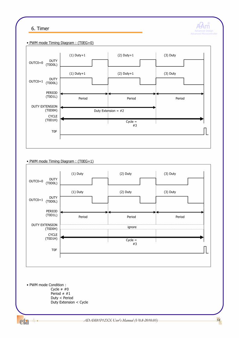
• PWM mode Timing Diagram : (T0EG=0)
(1) Duty+1 (2) Duty+1 (3) Duty
DUTY(T0D0L)
(1) Duty+1 (2) Duty+1 (3) Duty
DUTY(T0D0L)OUTC0=0
OUTC0=1
Cycle = #3
Period Period Period
Duty Extension = #2
CYCLE(T0D1H)
DUTY EXTENSION(T0D0H)
PERIOD(T0D1L)
T0F
• PWM mode Timing Diagram : (T0EG=1)
(1) Duty (2) Duty (3) Duty
DUTY(T0D0L)
(1) Duty (2) Duty (3) Duty
DUTY(T0D0L)OUTC0=0
OUTC0=1
Cycle = #3
Period Period Period
ignore
CYCLE(T0D1H)
DUTY EXTENSION(T0D0H)
PERIOD(T0D1L)
• PWM mode Condition :
T0F
58ADAM81P12XX User's Manual (V0.8-2010.05)
Cycle ≠ #0Period ≠ #1Duty < PeriodDuty Extension < Cycle

ADAm®
Advanced DesignAdvanced Microcontroller
6. Timer
T0CS (Cl & St t d t f b ff t )
• PWM mode Timing Diagram : (T0EG=0, DUTY EXTENSION=0)
TCK
T0CS (Clear & Start, move data from buffer to reg.)
CYCLE(T0D1H) xx
DUTY EXTENSION(T0D0H) xx
01
00 00
01
00 00
01
00 00
01
00(T0D0H)
PERIOD(T0D1L)
DUTY(T0D0L)
xx
xx
02
01 01
T0F
02
01 01
02
01 01
02
01
CYCLE
T0(OUTC0=0)
T0(OUTC0=1)
• PWM mode Timing Diagram : (T0EG=1, DUTY EXTENSION=0)
TCK
T0CS (Clear & Start, move data from buffer to reg.)
CYCLE(T0D1H) xx
DUTY EXTENSION
01 01 01 01
DUTY EXTENSION(T0D0H)
PERIOD(T0D1L)
DUTY(T0D0L)
xx
xx
xx
00 00
01
00 00
T0F
00 00
01
00 00
00 00
01
00 00
00
01
00
CYCLET0F
T0(OUTC0=0)
T0(OUTC0=1)
59ADAM81P12XX User's Manual (V0.8-2010.05)
• PWM mode Condition :Cycle ≠ #0Period ≠ #1Duty < PeriodDuty Extension < Cycle
ADAm®
Advanced DesignAdvanced Microcontroller
6. Timer
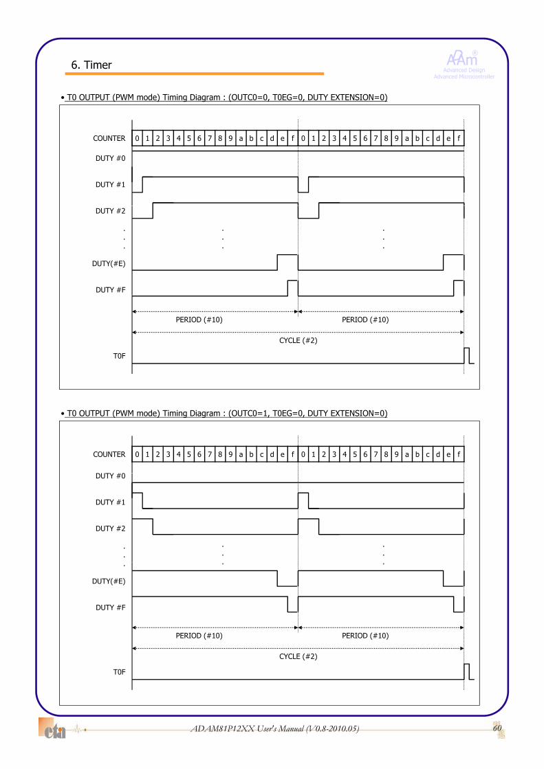
• T0 OUTPUT (PWM mode) Timing Diagram : (OUTC0=0, T0EG=0, DUTY EXTENSION=0)
0 1 2 3 4 5 6 7 8 9 a b c d e f
DUTY #0
DUTY #1
0 1 2 3 4 5 6 7 8 9 a b c d e fCOUNTER
DUTY #2
.
.
.
DUTY(#E)
DUTY #F
.
.
.
.
.
.
CYCLE (#2)
PERIOD (#10) PERIOD (#10)
T0F
0 1 2 3 4 5 6 7 8 9 a b c d e f
• T0 OUTPUT (PWM mode) Timing Diagram : (OUTC0=1, T0EG=0, DUTY EXTENSION=0)
DUTY #0
0 1 2 3 4 5 6 7 8 9 a b c d e fCOUNTER
DUTY #0
DUTY #1
DUTY #2
.
...
.
.
PERIOD (#10)
.
DUTY(#E)
DUTY #F
PERIOD (#10)
. .
60ADAM81P12XX User's Manual (V0.8-2010.05)
CYCLE (#2)
T0F

ADAm®
Advanced DesignAdvanced Microcontroller
6. Timer
• T0 OUTPUT (PWM mode) Timing Diagram : (OUTC0=0, T0EG=0, DUTY EXTENSION=1)
0 1 2 3 4 5 6 7 8 9 a b c d e f
DUTY #0
DUTY #1
0 1 2 3 4 5 6 7 8 9 a b c d e fCOUNTER
DUTY #2
.
.
.
DUTY(#E)
DUTY #F
.
.
.
.
.
.
Prohibited Value(Duty≠Period) Prohibited Value(Duty≠Period)
CYCLE (#2)
PERIOD (#10) PERIOD (#10)
T0F
• T0 OUTPUT (PWM mode) Timing Diagram : (OUTC0=1, T0EG=0, DUTY EXTENSION=1)
0 1 2 3 4 5 6 7 8 9 a b c d e f
DUTY #0
0 1 2 3 4 5 6 7 8 9 a b c d e fCOUNTER
DUTY #0
DUTY #1
DUTY #2
.
...
.
.
PERIOD (#10)
.
DUTY(#E)
DUTY #F
PERIOD (#10)
. .
Prohibited Value(Duty≠Period) Prohibited Value(Duty≠Period)
61ADAM81P12XX User's Manual (V0.8-2010.05)
CYCLE (#2)
T0F
ADAm®
Advanced DesignAdvanced Microcontroller
6. Timer
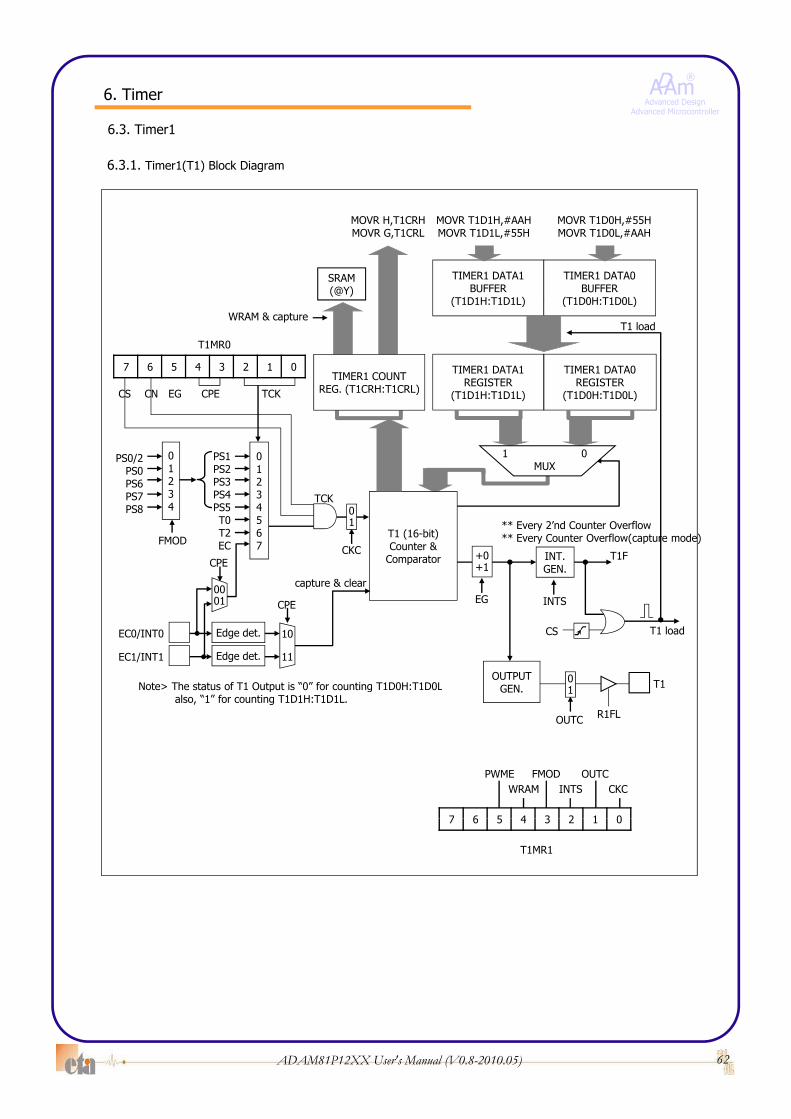
6.3. Timer1
6.3.1. Timer1(T1) Block Diagram
TIMER1 DATA1BUFFER
(T1D1H:T1D1L)
TIMER1 DATA0BUFFER
(T1D0H:T1D0L)
MOVR H,T1CRHMOVR G,T1CRL
MOVR T1D1H,#AAHMOVR T1D1L,#55H
MOVR T1D0H,#55HMOVR T1D0L,#AAH
SRAM(@Y)
( ) g
T1MR0
TIMER1 DATA1REGISTER
(T1D1H:T1D1L)
TIMER1 DATA0REGISTER
(T1D0H:T1D0L)
(T1D1H:T1D1L) (T1D0H:T1D0L)
T1 load
EG CPECS CN TCK
TIMER1 COUNTREG. (T1CRH:T1CRL)
WRAM & capture
7 6 5 4 3 2 1 0
T1F
TCK
INT.
T1 (16-bit)Counter &
Comparator
01234567
1 0MUX
PS1PS2PS3PS4PS5T0T2EC
CPE+0
01234
PS0/2PS0PS6PS7PS8
FMODCKC
01 ** Every 2’nd Counter Overflow
** Every Counter Overflow(capture mode)
T1FINT.GEN.
CS T1 load
OUTPUTGEN
Comparator
T1Note> The status of T1 Output is “0” for counting T1D0H:T1D0L
10
11
EC0/INT0 Edge det.
EC1/INT1 Edge det.
0001 CPE
capture & clear
CPE+0+1
EG INTS
01GEN.Note> The status of T1 Output is 0 for counting T1D0H:T1D0L
also, “1” for counting T1D1H:T1D1L.R1FL
PWMEWRAM
FMOD
7 6 5 4 3 2 1 0
INTSOUTC
CKC
OUTC
1
T1MR1
7 6 5 4 3 2 1 0
62ADAM81P12XX User's Manual (V0.8-2010.05)
ADAm®
Advanced DesignAdvanced Microcontroller
6. Timer
6.3.2. Timer1 Control Register
• Timer1 Mode Register 0 (T1MR0)
7 6 5 4 3 2 1 0
T1MR0 T1CS T1CN T1EG T1CPE1 T1CPE0 T1CK2 T1CK1 T1CK0 57h
initial value 0 0 0 0 0 0 0 0
g
R/W R/W R/W R/W R/W R/W R/W R/W R/W
Selection Mode of T1MR0
Bit Name Selection Mode Remarks
T1CS Timer1 Clear / start Control0 Timer1 Stop
1 Timer1 Clear and Start
(fOSC = 4MHz)
T1CN Timer1 Pause / Continue Control0 Timer1 Pause
1 Timer1 continue
T1EG Timer1 Count Control0 Timer1 Count
1 Timer1 Count + 1
T1CPE1 Input capture &
00 EC0
01 EC1T1CPE0 Event Count selection 10 Capture 0 (INT0)
11 Capture 1 (INT1)
T1CK2T1CK1 Input clock selection
000 PS1 (0.5us) *PS0/2 *FMODE
001 PS2 (1us) *PS0 (0.25us)
010 PS3 (2us) *PS6 (16us)
011 PS4 (4us) *PS7 (32us)T1CK1T1CK0
Input clock selection100 PS5 (8us) *PS8 (64us)
101 T0
110 T2
111 EC (EC0 or EC1)
63ADAM81P12XX User's Manual (V0.8-2010.05)

ADAm®
Advanced DesignAdvanced Microcontroller
6. Timer
• Timer1 Mode Register 1 (T1MR1)
7 6 5 4 3 2 1 07 6 5 4 3 2 1 0
T1MR1 - - PWME1 WRAM1 FMOD1 INTS1 OUTC1 CKC1 58h
initial value 0 0 0 0 0 0 0 0
R/W - - R/W R/W R/W R/W R/W R/W
Selection Mode of T1MR1
Bit Name Selection Mode Remarks
PWME1 Timer/PWM Mode Selection0 Timer1 Normal Mode
1 Timer1 PWM Mode
WRAM1 Automatically Save Capture data to RAM0 Disable
1 Timer1 Automatically Save Capture data to RAM
FMOD1 F t M d S l ti0 Timer1 Normal Mode
FMOD1 Fast Mode Selection1 Timer1 Fast Mode
INTS1 Timer1 Interrupt Overflow Control0 Timer1 Interrupt Every 2nd Overflow
1 Timer1 Interrupt Every Overflow
OUTC1 Timer1 Output Control0 Timer1 Output Normal
1 Timer1 Output Reverse
0 Timer1 Input Clock NormalCKC1 Timer1 Input Clock Control
p
1 Timer1 Input Clock Reverse
Note: 16bit Timer : Save 2bytes capture data to RAM (2cycle) - addressed by @Y++.
0 1 2 3 4 5 6 7SRAM(@Y)
T1CRL T1CRH T1CRL T1CRH T1CRL T1CRH T1CRL T1CRH
1’st Captured Data 2’nd Captured Data 3’rd Captured Data 4’th Captured Data
64ADAM81P12XX User's Manual (V0.8-2010.05)

ADAm®
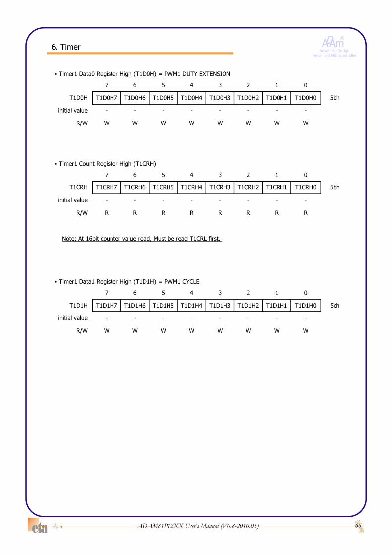
Advanced DesignAdvanced Microcontroller
6. Timer
• Timer1 Data0 Register Low (T1D0L) = PWM1 DUTY
7 6 5 4 3 2 1 07 6 5 4 3 2 1 0
T1D0L T1D0L7 T1D0L6 T1D0L5 T1D0L4 T1D0L3 T1D0L2 T1D0L1 T1D0L0 59h
initial value - - - - - - - -
R/W W W W W W W W W
• Timer1 Count Register Low (T1CRL)
7 6 5 4 3 2 1 0
T1CRL T1CRL7 T1CRL6 T1CRL5 T1CRL4 T1CRL3 T1CRL2 T1CRL1 T1CRL0 59h
initial value - - - - - - - -
R/W R R R R R R R RR/W R R R R R R R R
• Timer1 Data1 Register Low (T1D1L) = PWM1 PERIOD
Note: At 16bit counter value read, Must be read T1CRL first.
• Timer1 Data1 Register Low (T1D1L) = PWM1 PERIOD
7 6 5 4 3 2 1 0
T1D1L T1D1L7 T1D1L6 T1D1L5 T1D1L4 T1D1L3 T1D1L2 T1D1L1 T1D1L0 5ah
initial value - - - - - - - -
R/W W W W W W W W W
65ADAM81P12XX User's Manual (V0.8-2010.05)
ADAm®
Advanced DesignAdvanced Microcontroller
6. Timer
• Timer1 Data0 Register High (T1D0H) = PWM1 DUTY EXTENSION
7 6 5 4 3 2 1 07 6 5 4 3 2 1 0
T1D0H T1D0H7 T1D0H6 T1D0H5 T1D0H4 T1D0H3 T1D0H2 T1D0H1 T1D0H0 5bh
initial value - - - - - - - -
R/W W W W W W W W W
• Timer1 Count Register High (T1CRH)
7 6 5 4 3 2 1 0
T1CRH T1CRH7 T1CRH6 T1CRH5 T1CRH4 T1CRH3 T1CRH2 T1CRH1 T1CRH0 5bh
initial value - - - - - - - -
R/W R R R R R R R RR/W R R R R R R R R
Note: At 16bit counter value read, Must be read T1CRL first.
• Timer1 Data1 Register High (T1D1H) = PWM1 CYCLE
7 6 5 4 3 2 1 0
T1D1H T1D1H7 T1D1H6 T1D1H5 T1D1H4 T1D1H3 T1D1H2 T1D1H1 T1D1H0 5ch
initial value - - - - - - - -
R/W W W W W W W W W
66ADAM81P12XX User's Manual (V0.8-2010.05)
ADAm®
Advanced DesignAdvanced Microcontroller
6. Timer
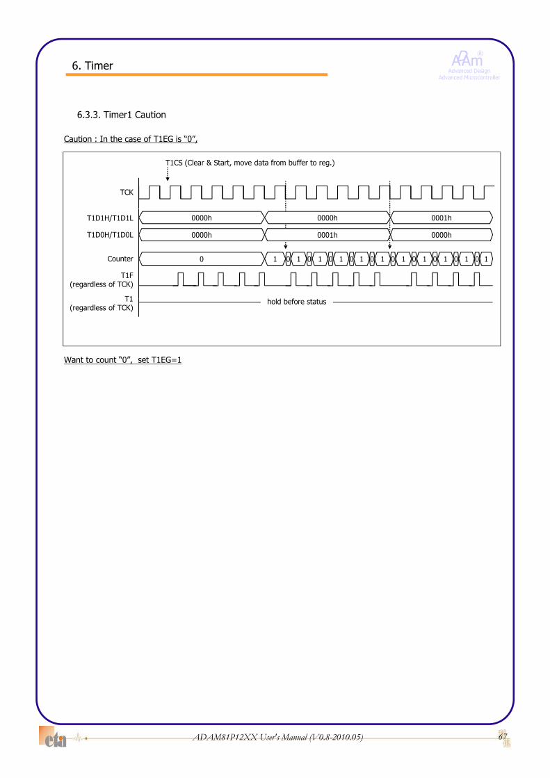
6.3.3. Timer1 Caution
TCK
T1CS (Clear & Start, move data from buffer to reg.)
Caution : In the case of T1EG is “0”,
T1F(regardless of TCK)
T1
T1D1H/T1D1L
T1D0H/T1D0L
0Counter
0000h
0000h
0000h
0001h
0001h
0000h
1 0 1 0 1 0 1 0 1 0 1 0 1 0 1 0 1 0 1 0 1
T1(regardless of TCK)
hold before status
Want to count “0”, set T1EG=1
67ADAM81P12XX User's Manual (V0.8-2010.05)

ADAm®
Advanced DesignAdvanced Microcontroller
6. Timer
* 16 bit Timer/Counter mode Timing Diagram
6.3.4. Timer1 Timing Diagram
* 16-bit Timer/Counter mode Timing Diagram
T1CS
T1D0H:T1D0L
TCK
T1CN
FFFFhT1D1H:T1D1L
T1D0H T1D0L
CS &Reload
T1Counter
0000hCS &Reload
CS &Reload
CS &Reload
T1D0H:T1D0L
Reload
Interval period
T1F
T1
Interval period
Reload Reload Reload
T1F(INTS1=1)
Note > CS : Timer1 Counter Clear & Start.Reload : Timer1 Data move from Data buffer to Data register.
* Start / Stop operation
(INTS1 1)
T1Counter
TCK
FFFFh
T1D0H:T0D0L T1D0H:T1D0L T1D0H:T1D0L
T1D1H:T1D1L
Counter
0000h
Pause
continue
T1CS
Stop Pause
continue
68ADAM81P12XX User's Manual (V0.8-2010.05)
T1CN
ADAm®
Advanced DesignAdvanced Microcontroller
6. Timer
T1CS (Clear & Start, move data from buffer to reg.)
* 16-bit Timer/Counter mode Timing Diagram
TCK
m qT1D1H:T1D1L
n pT1D0H:T1D0L
( g )
0
0
T1F (Clear & Start, move data from buffer to reg.)
T1F
T1
0 1 ~ 0 ~Counter n 0mn-1 m-1 1 ~ 0 ~p 0qp-1 q-1 1
clear clear
T1F(INTS1=1)
TCK
T1CS (Clear & Start, move data from buffer to reg.)
* 16-bit Capture mode Timing Diagram
TCK
T1D1H:T1D1L
T1D0H:T1D0L
0 1 ~ 0 1Counter 3 32 2 4 ~ 0 1FF 02FE 2
clear
-
T1F
1
match
don’t care --
00FFh -
INT0F or INT1F(rising edge)
INT0 or INT1
clear
T1CRH - 00 00
capture capture
T1CRL - 03 02
1’st Interrupt interval period= 03h
2’nd Interrupt interval period= FFh + 02h
capture capture
T1CRL T1CRH T1CRL T1CRH
WT(WRAM1=1)
69ADAM81P12XX User's Manual (V0.8-2010.05)
T1CRL
00 0201
T1CRH T1CRL T1CRH
03@Y

ADAm®
Advanced DesignAdvanced Microcontroller
6. Timer
• PWM mode Timing Diagram : (T1EG=0)
(1) Duty+1 (2) Duty+1 (3) Duty
DUTY(T1D0L)
(1) Duty+1 (2) Duty+1 (3) Duty
DUTY(T1D0L)OUTC1=0
OUTC1=1
Cycle = #3
Period Period Period
Duty Extension = #2
CYCLE(T1D1H)
DUTY EXTENSION(T1D0H)
PERIOD(T1D1L)
T1F
• PWM mode Timing Diagram : (T1EG=1)
(1) Duty (2) Duty (3) Duty
DUTY(T1D0L)
(1) Duty (2) Duty (3) Duty
DUTY(T1D0L)OUTC1=0
OUTC1=1
Cycle = #3
Period Period Period
ignore
CYCLE(T1D1H)
DUTY EXTENSION(T1D0H)
PERIOD(T1D1L)
• PWM mode Condition :
T1F
70ADAM81P12XX User's Manual (V0.8-2010.05)
Cycle ≠ #0Period ≠ #1Duty < PeriodDuty Extension < Cycle
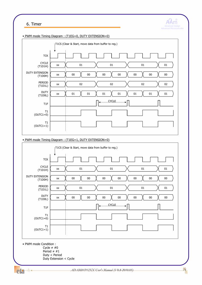
ADAm®
Advanced DesignAdvanced Microcontroller
6. Timer
T1CS (Cl & St t d t f b ff t )
• PWM mode Timing Diagram : (T1EG=0, DUTY EXTENSION=0)
TCK
T1CS (Clear & Start, move data from buffer to reg.)
CYCLE(T1D1H) xx
DUTY EXTENSION(T1D0H) xx
01
00 00
01
00 00
01
00 00
01
00(T1D0H)
PERIOD(T1D1L)
DUTY(T1D0L)
xx
xx
02
01 01
T1F
02
01 01
02
01 01
02
01
CYCLE
T1(OUTC1=0)
T1(OUTC1=1)
• PWM mode Timing Diagram : (T1EG=1, DUTY EXTENSION=0)
TCK
T1CS (Clear & Start, move data from buffer to reg.)
CYCLE(T1D1H) xx
DUTY EXTENSION
01 01 01 01
DUTY EXTENSION(T1D0H)
PERIOD(T1D1L)
DUTY(T1D0L)
xx
xx
xx
00 00
01
00 00
T1F
00 00
01
00 00
00 00
01
00 00
00
01
00
CYCLET1F
T1(OUTC1=0)
T1(OUTC1=1)
71ADAM81P12XX User's Manual (V0.8-2010.05)
• PWM mode Condition :Cycle ≠ #0Period ≠ #1Duty < PeriodDuty Extension < Cycle

ADAm®
Advanced DesignAdvanced Microcontroller
6. Timer
• T1 OUTPUT (PWM mode) Timing Diagram : (OUTC1=0, T1EG=0, DUTY EXTENSION=0)
0 1 2 3 4 5 6 7 8 9 a b c d e f
DUTY #0
DUTY #1
0 1 2 3 4 5 6 7 8 9 a b c d e fCOUNTER
DUTY #2
.
.
.
DUTY(#E)
DUTY #F
.
.
.
.
.
.
CYCLE (#2)
PERIOD (#10) PERIOD (#10)
T1F
0 1 2 3 4 5 6 7 8 9 a b c d e f
• T1 OUTPUT (PWM mode) Timing Diagram : (OUTC1=1, T1EG=0, DUTY EXTENSION=0)
DUTY #0
0 1 2 3 4 5 6 7 8 9 a b c d e fCOUNTER
DUTY #0
DUTY #1
DUTY #2
.
...
.
.
PERIOD (#10)
.
DUTY(#E)
DUTY #F
PERIOD (#10)
. .
72ADAM81P12XX User's Manual (V0.8-2010.05)
CYCLE (#2)
T1F

ADAm®
Advanced DesignAdvanced Microcontroller
6. Timer
• T1 OUTPUT (PWM mode) Timing Diagram : (OUTC1=0, T1EG=0, DUTY EXTENSION=1)
0 1 2 3 4 5 6 7 8 9 a b c d e f
DUTY #0
DUTY #1
0 1 2 3 4 5 6 7 8 9 a b c d e fCOUNTER
DUTY #2
.
.
.
DUTY(#E)
DUTY #F
.
.
.
.
.
.
Prohibited Value(Duty≠Period) Prohibited Value(Duty≠Period)
CYCLE (#2)
PERIOD (#10) PERIOD (#10)
T1F
• T1 OUTPUT (PWM mode) Timing Diagram : (OUTC1=1, T1EG=0, DUTY EXTENSION=1)
0 1 2 3 4 5 6 7 8 9 a b c d e f
DUTY #0
0 1 2 3 4 5 6 7 8 9 a b c d e fCOUNTER
DUTY #0
DUTY #1
DUTY #2
.
...
.
.
PERIOD (#10)
.
DUTY(#E)
DUTY #F
PERIOD (#10)
. .
Prohibited Value(Duty≠Period) Prohibited Value(Duty≠Period)
73ADAM81P12XX User's Manual (V0.8-2010.05)
CYCLE (#2)
T1F

ADAm®
Advanced DesignAdvanced Microcontroller
6. Timer
6.4. Timer2
6.4.1. Timer2(T2) Block Diagram
TIMER2 DATA1BUFFER
(T2D1H:T2D1L)
TIMER2 DATA0BUFFER
(T2D0H:T2D0L)
MOVR H,T2CRHMOVR G,T2CRL
MOVR T2D1H,#AAHMOVR T2D1L,#55H
MOVR T2D0H,#55HMOVR T2D0L,#AAH
SRAM(@Y)
( ) g
T2MR0
TIMER2 DATA1REGISTER
(T2D1H:T2D1L)
TIMER2 DATA0REGISTER
(T2D0H:T2D0L)
(T2D1H:T2D1L) (T2D0H:T2D0L)
T2 load
EG CPECS CN TCK
TIMER2 COUNTREG. (T2CRH:T2CRL)
WRAM & capture
7 6 5 4 3 2 1 0
T2F
TCK
INT.
T2 (16-bit)Counter &
Comparator
01234567
1 0MUX
PS1PS2PS3PS4PS5T0T1EC
CPE+0
01234
PS0/2PS0PS6PS7PS8
FMODCKC
01
0S C
** Every 2’nd Counter Overflow** Every Counter Overflow(capture mode)
INT.GEN.
CS T2 load
OUTPUTGEN
Comparator
T2Note> The status of T2 Output is “0” for counting T2D0H:T2D0L
10
11
EC1/INT1 Edge det.
EC2/INT2 Edge det.
0001 CPE
capture & clear
CPE +1
EG INTS
01
SPICKS
01SPICK
GEN.Note> The status of T2 Output is 0 for counting T2D0H:T2D0Lalso, “1” for counting T2D1H:T2D1L.
R2FN
TMCPWME
WRAMFMOD
7 6 5 4 3 2 1 0
INTSOUTC
CKC
OUTC
1
T2MR1
7 6 5 4 3 2 1 0
74ADAM81P12XX User's Manual (V0.8-2010.05)

ADAm®
Advanced DesignAdvanced Microcontroller
6. Timer
6.4.2. Timer2 Control Register
• Timer2 Mode Register 0 (T2MR0)
7 6 5 4 3 2 1 0
T2MR0 T2CS T2CN T2EG T2CPE1 T2CPE0 T2CK2 T2CK1 T2CK0 5dh
initial value 0 0 0 0 0 0 0 0
g
R/W R/W R/W R/W R/W R/W R/W R/W R/W
Selection Mode of T2MR0
Bit Name Selection Mode Remarks
T2CS Timer2 Clear / start Control0 Timer2 Stop
1 Timer2 Clear and Start
(fOSC = 4MHz)
T2CN Timer2 Pause / Continue Control0 Timer2 Pause
1 Timer2 continue
T2EG Timer2 Count Control0 Timer2 Count
1 Timer2 Count + 1
T2CPE1 Input capture &
00 EC1
01 EC2T2CPE0 Event Count selection 10 Capture 0 (INT1)
11 Capture 1 (INT2)
T2CK2
000 PS1 (0.5us) *PS0/2 *FMODE
001 PS2 (1us) *PS0 (0.25us)
010 PS3 (2us) *PS6 (16us)
011 PS4 (4us) *PS7 (32us)T2CK1T2CK0
Input clock selection 100 PS5 (8us) *PS8 (64us)
101 T0
110 T1SPICK (@SPICKS=1)
111 EC (EC1 or EC2)
75ADAM81P12XX User's Manual (V0.8-2010.05)
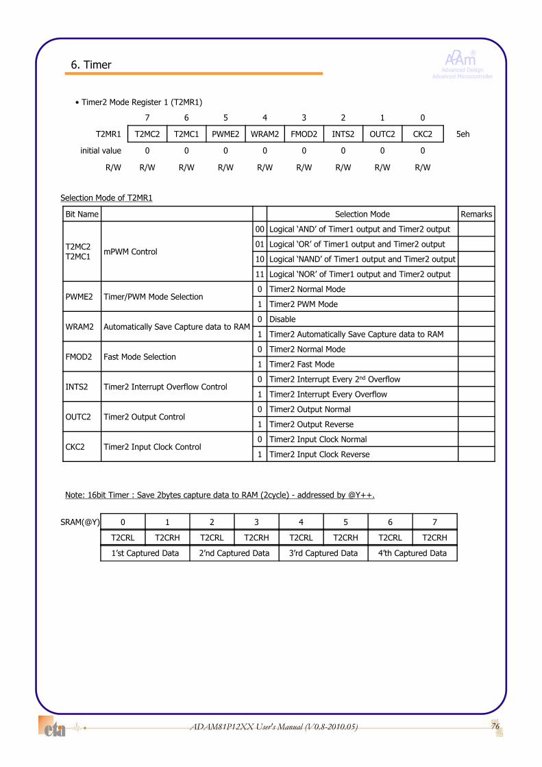
ADAm®
Advanced DesignAdvanced Microcontroller
6. Timer
• Timer2 Mode Register 1 (T2MR1)
7 6 5 4 3 2 1 07 6 5 4 3 2 1 0
T2MR1 T2MC2 T2MC1 PWME2 WRAM2 FMOD2 INTS2 OUTC2 CKC2 5eh
initial value 0 0 0 0 0 0 0 0
R/W R/W R/W R/W R/W R/W R/W R/W R/W
Selection Mode of T2MR1
Bit Name Selection Mode Remarks
T2MC2T2MC1 mPWM Control
00 Logical ‘AND’ of Timer1 output and Timer2 output
01 Logical ‘OR’ of Timer1 output and Timer2 output
10 Logical ‘NAND’ of Timer1 output and Timer2 output
11 Logical ‘NOR’ of Timer1 output and Timer2 output
PWME2 Ti /PWM M d S l ti0 Timer2 Normal Mode
PWME2 Timer/PWM Mode Selection1 Timer2 PWM Mode
WRAM2 Automatically Save Capture data to RAM0 Disable
1 Timer2 Automatically Save Capture data to RAM
FMOD2 Fast Mode Selection0 Timer2 Normal Mode
1 Timer2 Fast Mode
0 Timer2 Interrupt Every 2nd OverflowINTS2 Timer2 Interrupt Overflow Control
p y
1 Timer2 Interrupt Every Overflow
OUTC2 Timer2 Output Control0 Timer2 Output Normal
1 Timer2 Output Reverse
CKC2 Timer2 Input Clock Control0 Timer2 Input Clock Normal
1 Timer2 Input Clock Reverse
Note: 16bit Timer : Save 2bytes capture data to RAM (2cycle) - addressed by @Y++.
0 1 2 3 4 5 6 7SRAM(@Y)
T2CRL T2CRH T2CRL T2CRH T2CRL T2CRH T2CRL T2CRH
1’st Captured Data 2’nd Captured Data 3’rd Captured Data 4’th Captured Data
76ADAM81P12XX User's Manual (V0.8-2010.05)
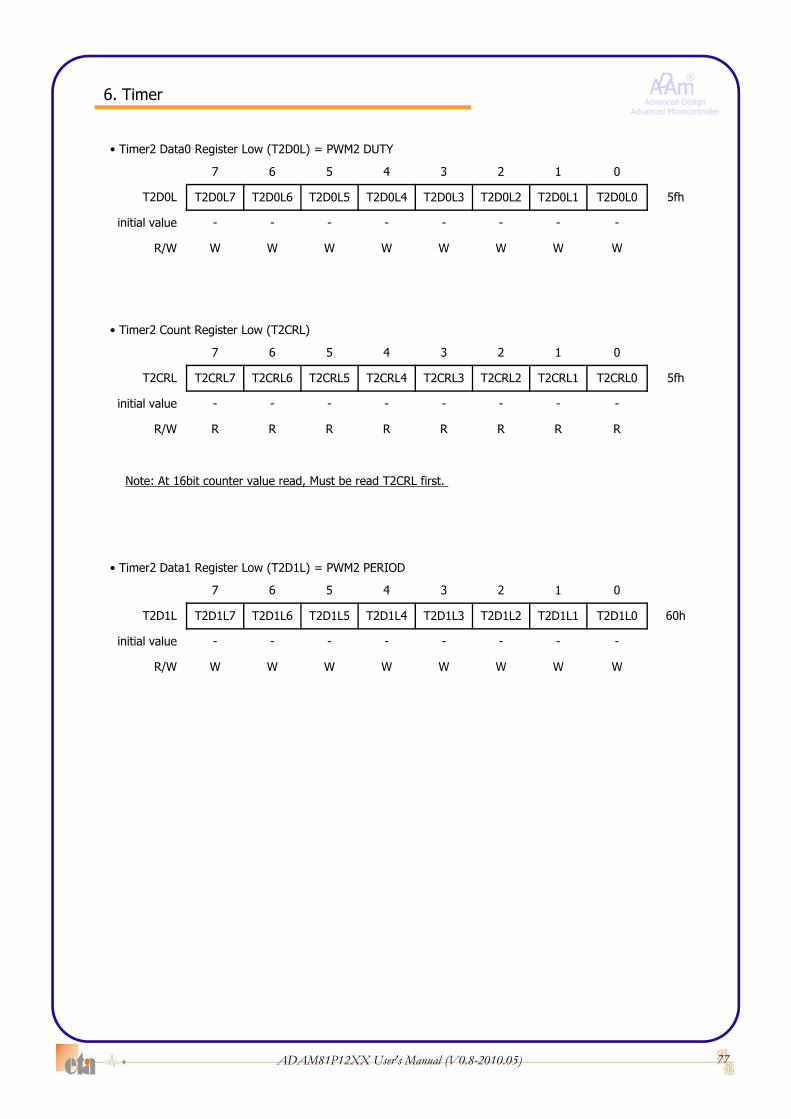
ADAm®
Advanced DesignAdvanced Microcontroller
6. Timer
• Timer2 Data0 Register Low (T2D0L) = PWM2 DUTY
7 6 5 4 3 2 1 07 6 5 4 3 2 1 0
T2D0L T2D0L7 T2D0L6 T2D0L5 T2D0L4 T2D0L3 T2D0L2 T2D0L1 T2D0L0 5fh
initial value - - - - - - - -
R/W W W W W W W W W
• Timer2 Count Register Low (T2CRL)
7 6 5 4 3 2 1 0
T2CRL T2CRL7 T2CRL6 T2CRL5 T2CRL4 T2CRL3 T2CRL2 T2CRL1 T2CRL0 5fh
initial value - - - - - - - -
R/W R R R R R R R RR/W R R R R R R R R
Note: At 16bit counter value read, Must be read T2CRL first.
• Timer2 Data1 Register Low (T2D1L) = PWM2 PERIOD
7 6 5 4 3 2 1 0
T2D1L T2D1L7 T2D1L6 T2D1L5 T2D1L4 T2D1L3 T2D1L2 T2D1L1 T2D1L0 60h
initial value - - - - - - - -
R/W W W W W W W W W
77ADAM81P12XX User's Manual (V0.8-2010.05)

ADAm®
Advanced DesignAdvanced Microcontroller
6. Timer
• Timer2 Data0 Register High (T2D0H) = PWM2 DUTY EXTENSION
7 6 5 4 3 2 1 07 6 5 4 3 2 1 0
T2D0H T2D0H7 T2D0H6 T2D0H5 T2D0H4 T2D0H3 T2D0H2 T2D0H1 T2D0H0 61h
initial value - - - - - - - -
R/W W W W W W W W W
• Timer2 Count Register High (T2CRH)
7 6 5 4 3 2 1 0
T2CRH T2CRH7 T2CRH6 T2CRH5 T2CRH4 T2CRH3 T2CRH2 T2CRH1 T2CRH0 61h
initial value - - - - - - - -
R/W R R R R R R R RR/W R R R R R R R R
• Timer2 Data1 Register High (T2D1H) = PWM2 CYCLE
Note: At 16bit counter value read, Must be read T2CRL first.
• Timer2 Data1 Register High (T2D1H) = PWM2 CYCLE
7 6 5 4 3 2 1 0
T2D1H T2D1H7 T2D1H6 T2D1H5 T2D1H4 T2D1H3 T2D1H2 T2D1H1 T2D1H0 62h
initial value - - - - - - - -
R/W W W W W W W W W
78ADAM81P12XX User's Manual (V0.8-2010.05)

ADAm®
Advanced DesignAdvanced Microcontroller
6. Timer
6.4.3. Timer2 Caution
TCK
T2CS (Clear & Start, move data from buffer to reg.)
Caution : In the case of T2EG is “0”,
T2F(regardless of TCK)
T2
T2D1H/T2D1L
T2D0H/T2D0L
0Counter
0000h
0000h
0000h
0001h
0001h
0000h
1 0 1 0 1 0 1 0 1 0 1 0 1 0 1 0 1 0 1 0 1
T2(regardless of TCK)
hold before status
Want to count “0”, set T2EG=1
79ADAM81P12XX User's Manual (V0.8-2010.05)

ADAm®
Advanced DesignAdvanced Microcontroller
6. Timer
6.4.4. TM12 Mode
* TM12 Logical Output Control
T1
T2TMC[2:1]
00
01
10
11
TM12
* TM12 mode Timing Diagram
T1
TMC
TM12 mode Timing Diagram
0 (AND)
T2
1 (OR) 2 (NAND) 3 (NOR)
TM12
80ADAM81P12XX User's Manual (V0.8-2010.05)
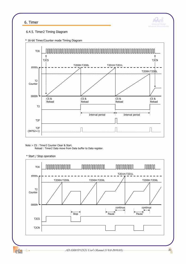
ADAm®
Advanced DesignAdvanced Microcontroller
6. Timer
* 16 bit Timer/Counter mode Timing Diagram
6.4.5. Timer2 Timing Diagram
* 16-bit Timer/Counter mode Timing Diagram
T2CS
T2D0H:T2D0L
TCK
T2CN
FFFFhT2D1H:T2D1L
T2D0H T2D0L
CS &Reload
T2Counter
0000hCS &Reload
CS &Reload
CS &Reload
T2D0H:T2D0L
Reload
Interval period
T2F
T2
Interval period
Reload Reload Reload
T2F(INTS2=1)
Note > CS : Timer2 Counter Clear & Start.Reload : Timer2 Data move from Data buffer to Data register.
* Start / Stop operation
(INTS2 1)
T2Counter
TCK
FFFFh
T2D0H:T2D0L T2D0H:T2D0L T2D0H:T2D0L
T2D1H:T2D1L
Counter
0000h
Pause
continue
T2CS
Stop Pause
continue
81ADAM81P12XX User's Manual (V0.8-2010.05)
T2CN

ADAm®
Advanced DesignAdvanced Microcontroller
6. Timer
T2CS (Clear & Start, move data from buffer to reg.)
* 16-bit Timer/Counter mode Timing Diagram
TCK
m qT2D1H:T2D1L
n pT2D0H:T2D0L
( g )
0
0
T2F (Clear & Start, move data from buffer to reg.)
T2F
T2
0 1 ~ 0 ~Counter n 0mn-1 m-1 1 ~ 0 ~p 0qp-1 q-1 1
clear clear
T2F(INTS2=1)
TCK
T2CS (Clear & Start, move data from buffer to reg.)
* 16-bit Capture mode Timing Diagram
TCK
T2D1H:T2D1L
T2D0H:T2D0L
0 1 ~ 0 1Counter 3 32 2 4 ~ 0 1FF 02FE 2
clear
-
T2F
1
match
don’t care --
00FFh -
INT1F or INT2F(rising edge)
INT1 or INT2
clear
T2CRH - 00 00
capture capture
T2CRL - 03 02
1’st Interrupt interval period= 03h
2’nd Interrupt interval period= FFh + 02h
capture capture
T2CRL T2CRH T2CRL T0CRH
WT(WRAM2=1)
82ADAM81P12XX User's Manual (V0.8-2010.05)
T2CRL
00 0201
T2CRH T2CRL T0CRH
03@Y

ADAm®
Advanced DesignAdvanced Microcontroller
6. Timer
• PWM mode Timing Diagram : (T2EG=0)
(1) Duty+1 (2) Duty+1 (3) Duty
DUTY(T2D0L)
(1) Duty+1 (2) Duty+1 (3) Duty
DUTY(T2D0L)OUTC2=0
OUTC2=1
Cycle = #3
Period Period Period
Duty Extension = #2
CYCLE(T2D1H)
DUTY EXTENSION(T2D0H)
PERIOD(T2D1L)
T2F
• PWM mode Timing Diagram : (T2EG=1)
(1) Duty (2) Duty (3) Duty
DUTY(T2D0L)
(1) Duty (2) Duty (3) Duty
DUTY(T2D0L)OUTC2=0
OUTC2=1
Cycle = #3
Period Period Period
ignore
CYCLE(T2D1H)
DUTY EXTENSION(T2D0H)
PERIOD(T2D1L)
• PWM mode Condition :
T2F
83ADAM81P12XX User's Manual (V0.8-2010.05)
Cycle ≠ #0Period ≠ #1Duty < PeriodDuty Extension < Cycle

ADAm®
Advanced DesignAdvanced Microcontroller
6. Timer
T2CS (Cl & St t d t f b ff t )
• PWM mode Timing Diagram : (T2EG=0, DUTY EXTENSION=0)
TCK
T2CS (Clear & Start, move data from buffer to reg.)
CYCLE(T2D1H) xx
DUTY EXTENSION(T2D0H) xx
01
00 00
01
00 00
01
00 00
01
00(T2D0H)
PERIOD(T2D1L)
DUTY(T2D0L)
xx
xx
02
01 01
T2F
02
01 01
02
01 01
02
01
CYCLE
T2(OUTC2=0)
T2(OUTC2=1)
• PWM mode Timing Diagram : (T2EG=1, DUTY EXTENSION=0)
TCK
T2CS (Clear & Start, move data from buffer to reg.)
CYCLE(T2D1H) xx
DUTY EXTENSION
01 01 01 01
DUTY EXTENSION(T2D0H)
PERIOD(T2D1L)
DUTY(T2D0L)
xx
xx
xx
00 00
01
00 00
T2F
00 00
01
00 00
00 00
01
00 00
00
01
00
CYCLET2F
T2(OUTC2=0)
T2(OUTC2=1)
84ADAM81P12XX User's Manual (V0.8-2010.05)
• PWM mode Condition :Cycle ≠ #0Period ≠ #1Duty < PeriodDuty Extension < Cycle

ADAm®
Advanced DesignAdvanced Microcontroller
6. Timer
• T2 OUTPUT (PWM mode) Timing Diagram : (OUTC2=0, T2EG=0, DUTY EXTENSION=0)
0 1 2 3 4 5 6 7 8 9 a b c d e f
DUTY #0
DUTY #1
0 1 2 3 4 5 6 7 8 9 a b c d e fCOUNTER
DUTY #2
.
.
.
DUTY(#E)
DUTY #F
.
.
.
.
.
.
CYCLE (#2)
PERIOD (#10) PERIOD (#10)
T2F
0 1 2 3 4 5 6 7 8 9 a b c d e f
• T2 OUTPUT (PWM mode) Timing Diagram : (OUTC2=1, T2EG=0, DUTY EXTENSION=0)
DUTY #0
0 1 2 3 4 5 6 7 8 9 a b c d e fCOUNTER
DUTY #0
DUTY #1
DUTY #2
.
...
.
.
PERIOD (#10)
.
DUTY(#E)
DUTY #F
PERIOD (#10)
. .
85ADAM81P12XX User's Manual (V0.8-2010.05)
CYCLE (#2)
T2F
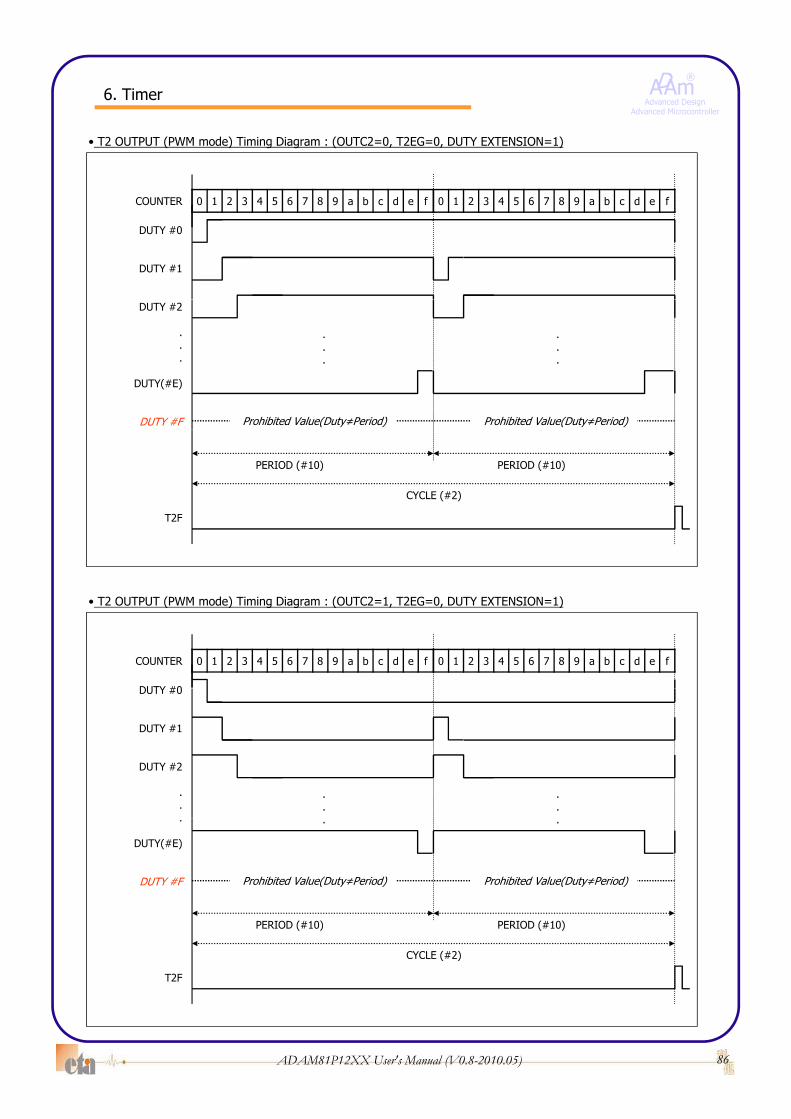
ADAm®
Advanced DesignAdvanced Microcontroller
6. Timer
• T2 OUTPUT (PWM mode) Timing Diagram : (OUTC2=0, T2EG=0, DUTY EXTENSION=1)
0 1 2 3 4 5 6 7 8 9 a b c d e f
DUTY #0
DUTY #1
0 1 2 3 4 5 6 7 8 9 a b c d e fCOUNTER
DUTY #2
.
.
.
DUTY(#E)
DUTY #F
.
.
.
.
.
.
Prohibited Value(Duty≠Period) Prohibited Value(Duty≠Period)
CYCLE (#2)
PERIOD (#10) PERIOD (#10)
T2F
• T2 OUTPUT (PWM mode) Timing Diagram : (OUTC2=1, T2EG=0, DUTY EXTENSION=1)
0 1 2 3 4 5 6 7 8 9 a b c d e f
DUTY #0
0 1 2 3 4 5 6 7 8 9 a b c d e fCOUNTER
DUTY #0
DUTY #1
DUTY #2
.
...
.
.
PERIOD (#10)
.
DUTY(#E)
DUTY #F
PERIOD (#10)
. .
Prohibited Value(Duty≠Period) Prohibited Value(Duty≠Period)
86ADAM81P12XX User's Manual (V0.8-2010.05)
CYCLE (#2)
T2F
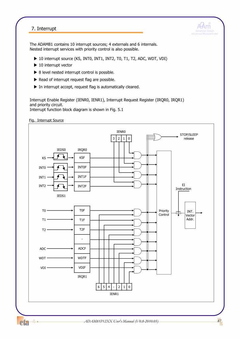
ADAm®
Advanced DesignAdvanced Microcontroller
The ADAM81 contains 10 interrupt sources; 4 externals and 6 internals.Nested interrupt services with priority control is also possible.
7. Interrupt
▶ 10 interrupt source (KS, INT0, INT1, INT2, T0, T1, T2, ADC, WDT, VDI)
▶ 10 interrupt vector
▶ 8 level nested interrupt control is possible.
▶ Read of interrupt request flag are possible.
▶ In interrupt accept, request flag is automatically cleared.
Interrupt Enable Register (IENR0, IENR1), Interrupt Request Register (IRQR0, IRQR1) and priority circuit.Interrupt function block diagram is shown in Fig. 5.1
Fig. Interrupt Source
IRQR0
STOP/SLEEP release
IENR0
3 2 1 0
KS
INT0
KSF
INT0F
IEDS0
INT1 INT1F
INT2F EI Instruction
INT2
IEDS1
PriorityControl
INT.VectorAddr.
T0F
T1F
T2F
-
ADCF
T0
T1
T2
ADC
6 5 4 - 2 1 0
ADCF
WDTF
VDIF
IRQR1
ADC
WDT
VDI
87ADAM81P12XX User's Manual (V0.8-2010.05)
IENR1
6 5 4 2 1 0

ADAm®
Advanced DesignAdvanced Microcontroller
7.1. Interrupt Source
Each interrupt vector is independent and has its own priority.
7. Interrupt
After internal reset is released, RESET vector Address is 0000h thus program start point should be defined as follows (also interrupt):
Example : ORG 0000h
vRESET: MOVPG #0HBR !PGM_START ORG INT_ADDR
vKS: MOVPG #0H INT_KS: JOB_TO_WORKBR !INT KS RETIBR !INT_KS RETI
vINT0: MOVPG #0H INT_INT0: JOB_TO_WORKBR !INT_INT0 RETI
vINT1: MOVPG #0H INT_INT1: JOB_TO_WORKBR !INT_INT1 RETI
vINT2: MOVPG #0H INT_INT2: JOB_TO_WORK BR !!INT_INT2 RETI
vT0: MOVPG #0H INT_T0: JOB_TO_WORK BR !INT_T0 RETI
vT1: MOVPG #0H INT T1: JOB TO WORKvT1: MOVPG #0H INT_T1: JOB_TO_WORK BR !INT_T1 RETI
vT2: MOVPG #0H INT_T2: JOB_TO_WORK BR !INT_T2 RETI
vADC: MOVPG #0H INT_ADC: JOB_TO_WORK BR !INT_ADC RETI
vWDT: MOVPG #0H INT_WDT: JOB_TO_WORK BR !INT_WDT RETI
vVDI: MOVPG #0H INT_VDI: JOB_TO_WORK BR !INT VDI RETI_
Table. Interrupt Source
Mask Priority Interrupt Source INT Vector Addr.
Non-maskable 0 RESET 0000h
1 KS 0002h
2 INT0 (External Interrupt 0) 0004h
3 INT1 (External Interrupt 1) 0006h
4 INT2 (External Interrupt 2) 0008h
5 - 000Ah
6 T0 (Timer0) 000Ch
HardwareInterrupt maskable
7 T1 (Timer1) 000Eh
8 T2 (Timer2) 0010h
9 - 0012h
10 ADC (Analog Digital Converter) 0014h
11 WDT ( Watch-Dog Timer) 0016h
12 VDI (Voltage Detection Indicator) 0018h
88ADAM81P12XX User's Manual (V0.8-2010.05)
13 - -
14 - -
15 - -

ADAm®
Advanced DesignAdvanced Microcontroller
I flag of SFR is a interrupt mask enable flag.
7.2. Interrupt Control Register
7. Interrupt
g p gWhen I flag = “0”, all interrupts become disable.When I flag = “1”, interrupts can be selectively enabled and disabled by contents ofcorresponding Interrupt Enable Register(IENR0, IENR1).When interrupt is occurred, interrupt request flag is set,and Interrupt request is detected at the edge of interrupt signal. The accepted interrupt request flag is automatically cleared during interrupt cycle process. The interrupt request flag maintains “1” until the interrupt is accepted or is cleared in program. In reset state, interrupt request flag register (IRQR0, IRQR1) is cleared to “0”. , p q g g ( Q , Q )It is possible to read the state of interrupt register and to manipulate the contents of register.
• External Interrupt Edge selection Register (IEDS0)
7 6 5 4 3 2 1 0
IEDS0 - - - - - - IEDK 40h
initial value - - - - - - 0 0
R/W - - - - - - W W
Bit Name Selection Mode Remarks
00 -
Selection Mode of IEDS0
IEDK
00 -
KS01 Falling Edge Selection
10 Rising Edge Selection
11 Both Edge Selection
89ADAM81P12XX User's Manual (V0.8-2010.05)
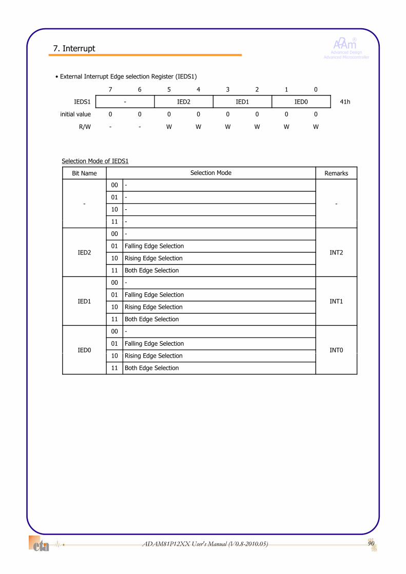
ADAm®
Advanced DesignAdvanced Microcontroller
7. Interrupt
• External Interrupt Edge selection Register (IEDS1)
7 6 5 4 3 2 1 07 6 5 4 3 2 1 0
IEDS1 - IED2 IED1 IED0 41h
initial value 0 0 0 0 0 0 0 0
R/W - - W W W W W W
Bit Name Selection Mode Remarks
-
00 -
-01 -
10 -
11
Selection Mode of IEDS1
11 -
IED2
00 -
INT201 Falling Edge Selection
10 Rising Edge Selection
11 Both Edge Selection
00 -
IED1 INT101 Falling Edge Selection
10 Rising Edge Selection
11 Both Edge Selection
IED0
00 -
INT001 Falling Edge Selection
d l10 Rising Edge Selection
11 Both Edge Selection
90ADAM81P12XX User's Manual (V0.8-2010.05)

ADAm®
Advanced DesignAdvanced Microcontroller
• Interrupt Enable Register (IENR0)
7 6 5 4 3 2 1 0
7. Interrupt
7 6 5 4 3 2 1 0
IENR0 - - - - INT2E INT1E INT0E KSE 42h
initial value 0 0 0 0 0 0 0 0
R/W - - - - R/W R/W R/W R/W
Selection Mode of IENR0
Bit Name Selection Mode Remarks
INT2E 1 External Interrupt 2 enable
INT1E 1 External Interrupt 1 enable
INT0E 1 External Interrupt 0 enable
KSE 1 Key Scan Interrupt enable
• Interrupt Request Flag Register (IRQR0)
7 6 5 4 3 2 1 0
IRQR0 - - - - INT2F INT1F INT0F KSF 43h
initial value 0 0 0 0 0 0 0 0
R/W - - - - R/W R/W R/W R/W
Bit Name Selection Mode Remarks
Selection Mode of IRQR0
INT2F 1 External Interrupt 2 Request enable
INT1F 1 External Interrupt 1 Request enable
INT0F 1 External Interrupt 0 Request enable
KSF 1 Key Scan Interrupt Request enable
91ADAM81P12XX User's Manual (V0.8-2010.05)
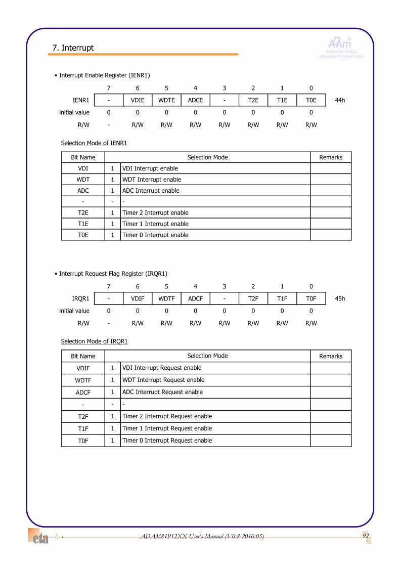
ADAm®
Advanced DesignAdvanced Microcontroller
• Interrupt Enable Register (IENR1)
7 6 5 4 3 2 1 0
7. Interrupt
7 6 5 4 3 2 1 0
IENR1 - VDIE WDTE ADCE - T2E T1E T0E 44h
initial value 0 0 0 0 0 0 0 0
R/W - R/W R/W R/W R/W R/W R/W R/W
Selection Mode of IENR1
Bit Name Selection Mode Remarks
VDI 1 VDI Interrupt enable
WDT 1 WDT Interrupt enable
ADC 1 ADC Interrupt enable
- - -
T2E 1 Timer 2 Interrupt enable
T1E 1 Timer 1 Interrupt enable
T0E 1 Timer 0 Interrupt enable
• Interrupt Request Flag Register (IRQR1)
7 6 5 4 3 2 1 0
IRQR1 - VDIF WDTF ADCF - T2F T1F T0F 45h
initial value 0 0 0 0 0 0 0 0
R/W - R/W R/W R/W R/W R/W R/W R/W
Selection Mode of IRQR1
Bit Name Selection Mode Remarks
VDIF 1 VDI Interrupt Request enable
WDTF 1 WDT Interrupt Request enable
ADCF 1 ADC Interrupt Request enable
- - -
1 Ti 2 I R blT2F 1 Timer 2 Interrupt Request enable
T1F 1 Timer 1 Interrupt Request enable
T0F 1 Timer 0 Interrupt Request enable
92ADAM81P12XX User's Manual (V0.8-2010.05)

ADAm®
Advanced DesignAdvanced Microcontroller
7.3. Interrupt Timing
Interrupt Request Sampling Time :
7. Interrupt
Interrupt Request Sampling Time :-. Maximum 2 machine cycle (2 machine cycle Instructions)
Interrupt preprocess step is 1 machine cycle
I flag is valid just after executing of EI/DI on the contrary
7.4. The valid timing after executing Interrupt control instructions
I flag is valid just after executing of EI/DI on the contrary.
7.5. Multiple Interrupt
If there is an interrupt, Interrupt Mask Enable Flag is automatically cleared before enteringthe Interrupt Service Routine. After then, no interrupt is accepted. If EI instruction is executed,interrupt mask enable bit becomes “1”, and each enable bit can accept interrupt request.Wh t i t t t d i lt l th hi h t i it i t t i t dWhen two or more interrupts are generated simultaneously, the highest priority interrupt is accepted.
Key-Scan or External Interrupt Enable Processing Step
1) Port Selection
2) Edge Selection
3) IRQR Clear
sabl
e Pr
oces
sing
Ste
p
4) IENR Setting
5) EI
Dis
93ADAM81P12XX User's Manual (V0.8-2010.05)
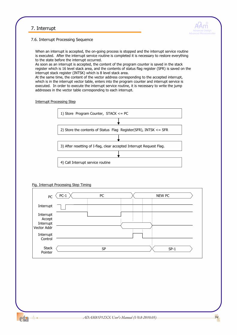
ADAm®
Advanced DesignAdvanced Microcontroller
When an interrupt is accepted the on going process is stopped and the interrupt service routine
7.6. Interrupt Processing Sequence
7. Interrupt
When an interrupt is accepted, the on-going process is stopped and the interrupt service routineis executed. After the interrupt service routine is completed it is necessary to restore everythingto the state before the interrupt occurred.As soon as an interrupt is accepted, the content of the program counter is saved in the stackregister which is 16 level stack area, and the contents of status flag register (SFR) is saved on the interrupt stack register (INTSK) which is 8 level stack area. At the same time, the content of the vector address corresponding to the accepted interrupt,which is in the interrupt vector table, enters into the program counter and interrupt service isexecuted. In order to execute the interrupt service routine, it is necessary to write the jumpaddresses in the vector table corresponding to each interruptaddresses in the vector table corresponding to each interrupt.
Interrupt Processing Step
1) Store Program Counter, STACK <= PC
2) S h f S Fl R i (SFR) INTSK SFR2) Store the contents of Status Flag Register(SFR), INTSK <= SFR
3) After resetting of I-flag, clear accepted Interrupt Request Flag.
4) Call Interrupt service routine
Fig. Interrupt Processing Step Timing
PC-1
Interrupt
PC PC NEW PC
Interrupt
InterruptAccept
InterruptVector Addr
InterruptControl
SP-1StackPointer
SP
94ADAM81P12XX User's Manual (V0.8-2010.05)
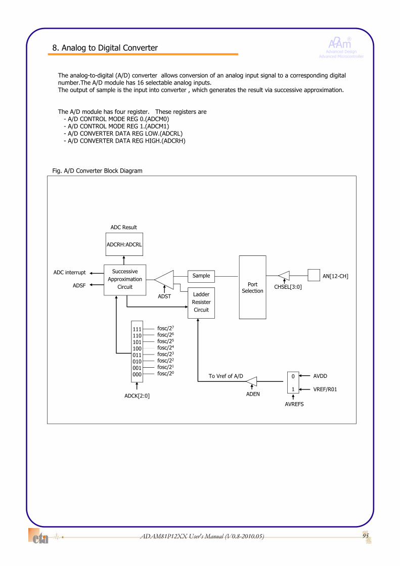
ADAm®
Advanced DesignAdvanced Microcontroller
The analog-to-digital (A/D) converter allows conversion of an analog input signal to a corresponding digital number.The A/D module has 16 selectable analog inputs.
8. Analog to Digital Converter
g pThe output of sample is the input into converter , which generates the result via successive approximation.
The A/D module has four register. These registers are- A/D CONTROL MODE REG 0.(ADCM0)- A/D CONTROL MODE REG 1.(ADCM1)- A/D CONVERTER DATA REG LOW.(ADCRL)- A/D CONVERTER DATA REG HIGH.(ADCRH)
Fig. A/D Converter Block Diagram
AN[12-CH]SampleADC interrupt
ADC Result
SuccessiveApproximation
ADCRH:ADCRL
P t CHSEL[3:0]LadderResisterCircuit
ADSF
ADST
Circuit
111110101100
fosc/27
fosc/26
fosc/25
fosc/24
PortSelection
AVDDTo Vref of A/D
ADEN
100011010001000
ADCK[2:0]
fosc/2fosc/23
fosc/22
fosc/21
fosc/200
1
AVREFS
VREF/R01
95ADAM81P12XX User's Manual (V0.8-2010.05)

ADAm®
Advanced DesignAdvanced Microcontroller
8. Analog to Digital Converter
8.1. A/D Converter Control Registers
7 6 5 4 3 2 1 0
ADCM0 - - - - - ADEN ADST ADSF 65h
initial value 0 0 0 0 0 0 0 1
• A/D Converter Mode Register (ADCM0)
R/W - - - - - R/W R/W R
Bit Name Selection Mode Remarks
ADEN0 ADC Disable if (STOP)
ADEN t “L”
Selection Mode of ADCM0
ADEN ADEN go to “L”1 ADC Enable
ADST0 A/D Conversion is Stop
1 A/D Conversion is Start.and cleared to “L” after 1 cycle
ADSF0 A/D Conversion is Processing
1 A/D Conversion is Completed
96ADAM81P12XX User's Manual (V0.8-2010.05)

ADAm®
Advanced DesignAdvanced Microcontroller
8. Analog to Digital Converter
• A/D Converter Mode Register (ADCM1)
7 6 5 4 3 2 1 0
ADCM1 CHSEL3 CHSEL2 CHSEL1 CHSEL0 ADCK2 ADCK1 ADCK0 AVREFS 67h
initial value 0 0 0 0 0 0 0 0
R/W W W W W W W W W
• A/D Converter Mode Register (ADCM1)
Bit Name Selection Mode Remarks
0000 Channel 0 Selection
0001 Channel 1 Selection
0010 Channel 2 Selection
Selection Mode of ADCM1 (fOSC = 4MHz)
CHSEL[3:0] if analog port selected
0011 Channel 3 Selection
0100 Channel 4 Selection
0101 Channel 5 Selection
0110 Channel 6 Selection
0111 Channel 7 Selection
1000 Channel 8 Selection
1001 Channel 9 Selection
1010 Channel 10 Selection
1011 Channel 11 Selection
1100 Channel 12 Selection
1101 Channel 13 Selection
1110 Channel 14 Selection
1111 Channel 15 Selection
ADCK[2:0]
000 PS0 (0.25us)
001 PS1 (0.5us)
010 PS2 (1us)
011 PS3 (2us)
100 PS4 (4us)( )
101 PS5 (8us)
110 PS6 (16us)
111 PS7 (32us)
AVREFS0 AVDD for ADC power
1 VREF for ADC power
97ADAM81P12XX User's Manual (V0.8-2010.05)

ADAm®
Advanced DesignAdvanced Microcontroller
8. Analog to Digital Converter
• A/D Converter Data Register Low (ADCRL)
7 6 5 4 3 2 1 0
ADCRL ADCRL7 ADCRL6 ADCRL5 ADCRL4 ADCRL3 ADCRL2 ADCRL1 ADCRL0 66h
initial value - - - - - - - -
R/W R R R R R R R R
A/D C t D t R i t Hi h (ADCRH)
7 6 5 4 3 2 1 0
ADCRH - - - - ADCRH3 ADCRH2 ADCRH1 ADCRH0 67h
initial value - - - - - - - -
R/W - - - - R R R R
• A/D Converter Data Register High (ADCRH)
ADC Timing Diagram
AVDD & CHSEL, ADCK
AVDD & CHSEL, ADCK SELECTION
ADEN
SADST
16*CKADCK 8*CK 8*CK 8*CK 8*CK ~ 8*CK
SETUP
ADCR
8*CK 8*CK 8*CK 4*CK
HOLDCONVERSION
11 10 9 8 ~ 3 2 1 0
ADSF
ADF
TOTAL116 * CK
• Total Conversion Time is
(16 + 8*12 + 4) * ADCK
Bit Name Selection Mode Remarks
freq = 4MHz
98ADAM81P12XX User's Manual (V0.8-2010.05)
ADCK000 Conversion Source Clock (1/fOSC) 116 * 250ns = 29us
010 Conversion Source Clock (22/fOSC) 116 * 1us = 116us
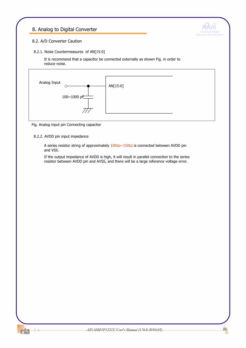
ADAm®
Advanced DesignAdvanced Microcontroller
8.2. A/D Converter Caution
8.2.1. Noise Countermeasures of AN[15:0]
8. Analog to Digital Converter
8.2.1. Noise Countermeasures of AN[15:0]
It is recommend that a capacitor be connected externally as shown Fig. in order to reduce noise.
AN[15:0]Analog Input
Fig. Analog input pin Connecting capacitor
100~1000 pF
8.2.2. AVDD pin input impedance
A series resistor string of approximately 100㏀~150㏀ is connected between AVDD pin and VSS.
If the output impedance of AVDD is high, it will result in parallel connection to the series resistor between AVDD pin and AVSS, and there will be a large reference voltage error.
99ADAM81P12XX User's Manual (V0.8-2010.05)

ADAm®
Advanced DesignAdvanced Microcontroller
8.3. A/D Converter Operation Flow
8. Analog to Digital Converter
SETR1 ADCM0 #2 ADC enable
MOVR ADCM1, #0XXH
AVREF selection.CHSEL[3:0] selection.ADCK selection.
SETR1 ADCM0.#1 A/D conversion Start
SETR1 ADCM0.#2 ADC enable
one or more NOP Wait for AN/AVREF stabilization Time
TSTR ADCM0.#0(ADSF==0 ?)
Check ADSF
NOYES
Read A/D Converter Result Read ADCRL, ADCRH
100ADAM81P12XX User's Manual (V0.8-2010.05)
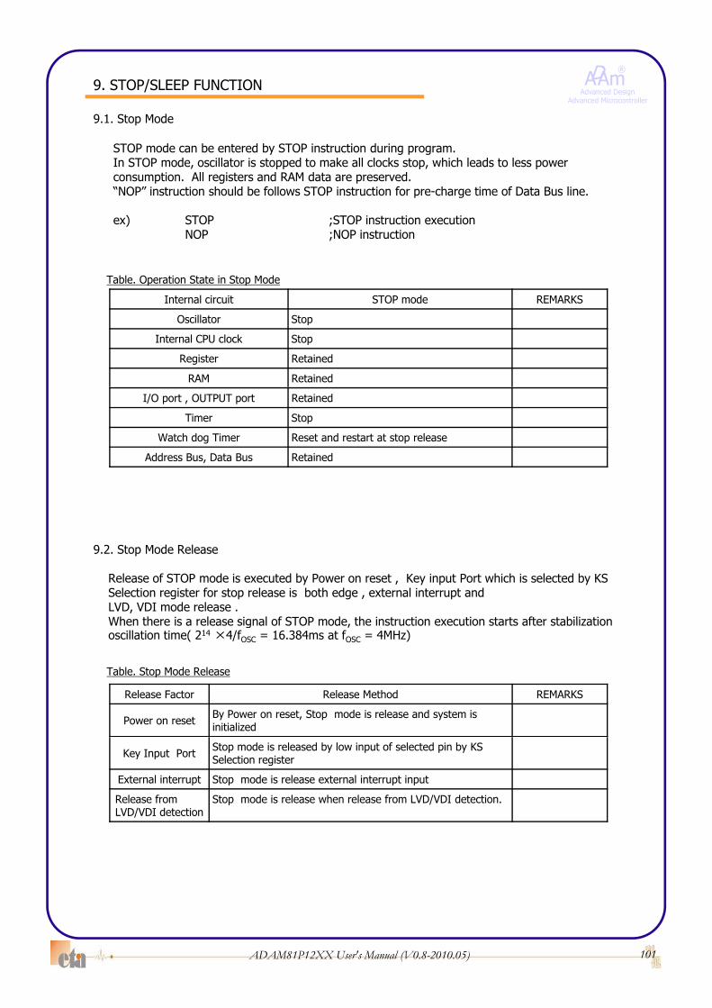
ADAm®
Advanced DesignAdvanced Microcontroller
STOP mode can be entered by STOP instruction during program.
9. STOP/SLEEP FUNCTION
9.1. Stop Mode
y g p gIn STOP mode, oscillator is stopped to make all clocks stop, which leads to less powerconsumption. All registers and RAM data are preserved.“NOP” instruction should be follows STOP instruction for pre-charge time of Data Bus line.
ex) STOP ;STOP instruction executionNOP ;NOP instruction
Table. Operation State in Stop Mode
Internal circuit STOP mode REMARKS
Oscillator Stop
Internal CPU clock Stop
Register Retained
RAM Retained
I/O port , OUTPUT port Retained
Timer Stop
Watch dog Timer Reset and restart at stop release
Address Bus, Data Bus Retained
Release of STOP mode is executed by Power on reset , Key input Port which is selected by KS Selection register for stop release is both edge , external interrupt and LVD, VDI mode release .When there is a release signal of STOP mode the instruction execution starts after stabilization
9.2. Stop Mode Release
When there is a release signal of STOP mode, the instruction execution starts after stabilization oscillation time( 214 ×4/fOSC = 16.384ms at fOSC = 4MHz)
Table. Stop Mode Release
Release Factor Release Method REMARKS
Power on reset By Power on reset, Stop mode is release and system is initialized
Key Input Port Stop mode is released by low input of selected pin by KS Selection register
External interrupt Stop mode is release external interrupt input
Release fromLVD/VDI detection
Stop mode is release when release from LVD/VDI detection.
101ADAM81P12XX User's Manual (V0.8-2010.05)
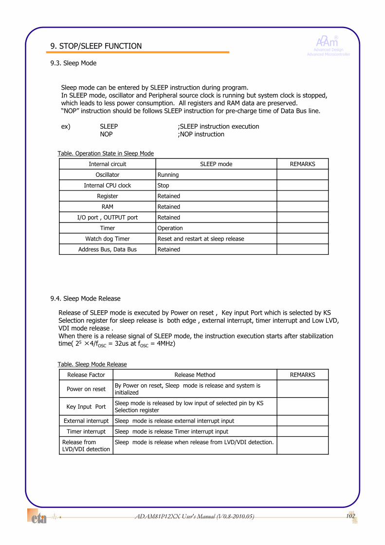
ADAm®
Advanced DesignAdvanced Microcontroller
9. STOP/SLEEP FUNCTION
9.3. Sleep Mode
Sleep mode can be entered by SLEEP instruction during program.In SLEEP mode, oscillator and Peripheral source clock is running but system clock is stopped, which leads to less power consumption. All registers and RAM data are preserved.“NOP” instruction should be follows SLEEP instruction for pre-charge time of Data Bus line.
ex) SLEEP ;SLEEP instruction executionNOP ;NOP instruction
Table. Operation State in Sleep Mode
Internal circuit SLEEP mode REMARKS
Oscillator Running
Internal CPU clock Stop
Register Retained
RAM Retained
I/O port , OUTPUT port Retained
Timer Operation
Watch dog Timer Reset and restart at sleep release
Address Bus, Data Bus Retained
Release of SLEEP mode is executed by Power on reset , Key input Port which is selected by KS Selection register for sleep release is both edge , external interrupt, timer interrupt and Low LVD, VDI mode release .When there is a release signal of SLEEP mode the instruction execution starts after stabilization
9.4. Sleep Mode Release
When there is a release signal of SLEEP mode, the instruction execution starts after stabilization time( 25 ×4/fOSC = 32us at fOSC = 4MHz)
Table. Sleep Mode Release
Release Factor Release Method REMARKS
Power on reset By Power on reset, Sleep mode is release and system is initialized
Key Input Port Sleep mode is released by low input of selected pin by KS Selection register
External interrupt Sleep mode is release external interrupt input
Timer interrupt Sleep mode is release Timer interrupt input
Release fromLVD/VDI detection
Sleep mode is release when release from LVD/VDI detection.
102ADAM81P12XX User's Manual (V0.8-2010.05)

ADAm®
Advanced DesignAdvanced Microcontroller
10. RESET FUNCTION
10.1. Power On RESET
Power On Reset circuit automatically detects the rise of power voltage(the rising time should be within 50ms). Until the power voltage reaches a certain voltage level, internal reset signal is maintained at “L” Level until oscillator is stable.After power applies and starting of oscillation, this reset state is maintained for about oscillation cycle of fosc/4 x216 (about 65.536ms : at 4MHz).
Fig. Block Diagram of Power On Reset Circuit
Internal Reset
VDD
Power On Detection Circuit
Fig. Oscillator stabilization diagram
VDD COUNT START
Notice. When Power On Reset, oscillator stabilization time doesn’t include OSC. Start time.
OSC. START TIMING
103ADAM81P12XX User's Manual (V0.8-2010.05)

ADAm®
Advanced DesignAdvanced Microcontroller
11.1. Low Voltage Detection Condition
11. Low Voltage Detection Mode
An on board voltage comparator checks that VDD is at the required level to ensure correct operation of the device. If VDD is below a certain level, Low voltage detector forces the device into low voltage detection mode.
11.2. Low Voltage Detection Mode
There is no power consumption except stop current.1. STOP mode release function is disabled.2. I/O port is configured as input mode.3. Data memory is retained until voltage through external capacitor is worn out.4. Interrupt disabled.5. Oscillator is stop.
11.3. Release of Low Voltage Detection Mode
Reset signal result from new battery or any other power (normally 3V/5V) wakes the low voltage detection mode and come into normal reset state. It depends on user whether to execute RAM clear routine or not.
11 4 Low Voltage Detection voltage selection (option)11.4. Low Voltage Detection voltage selection (option)
User can select the voltage of Low Voltage detection voltage level. One is high voltage version , another is low voltage version.
104ADAM81P12XX User's Manual (V0.8-2010.05)
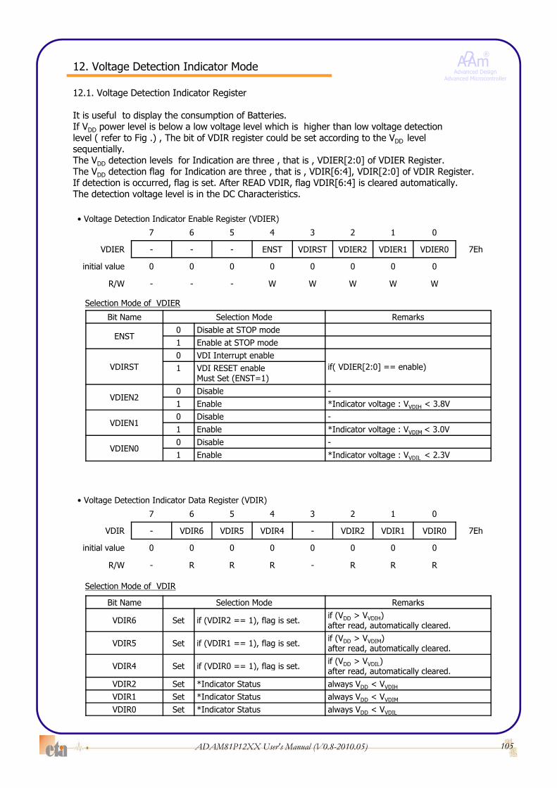
ADAm®
Advanced DesignAdvanced Microcontroller
12.1. Voltage Detection Indicator Register
It is useful to display the consumption of Batteries.
12. Voltage Detection Indicator Mode
p y pIf VDD power level is below a low voltage level which is higher than low voltage detectionlevel ( refer to Fig .) , The bit of VDIR register could be set according to the VDD level sequentially.The VDD detection levels for Indication are three , that is , VDIER[2:0] of VDIER Register.The VDD detection flag for Indication are three , that is , VDIR[6:4], VDIR[2:0] of VDIR Register. If detection is occurred, flag is set. After READ VDIR, flag VDIR[6:4] is cleared automatically.The detection voltage level is in the DC Characteristics.
• Voltage Detection Indicator Enable Register (VDIER)
7 6 5 4 3 2 1 0
VDIER - - - ENST VDIRST VDIER2 VDIER1 VDIER0 7Eh
initial value 0 0 0 0 0 0 0 0
R/W - - - W W W W W
Selection Mode of VDIERSelection Mode of VDIER
Bit Name Selection Mode Remarks
ENST0 Disable at STOP mode1 Enable at STOP mode
VDIRST0 VDI Interrupt enable
if( VDIER[2:0] == enable)1 VDI RESET enableMust Set (ENST=1)
0 Disable -VDIEN2
0 Disable1 Enable *Indicator voltage : VVDIH < 3.8V
VDIEN10 Disable -1 Enable *Indicator voltage : VVDIM < 3.0V
VDIEN00 Disable -1 Enable *Indicator voltage : VVDIL < 2.3V
• Voltage Detection Indicator Data Register (VDIR)
7 6 5 4 3 2 1 0
VDIR - VDIR6 VDIR5 VDIR4 - VDIR2 VDIR1 VDIR0 7Eh
initial value 0 0 0 0 0 0 0 0
R/W - R R R - R R R
Selection Mode of VDIR
Bit Name Selection Mode Remarks
VDIR6 Set if (VDIR2 == 1), flag is set. if (VDD > VVDIH)after read, automatically cleared.
VDIR5 Set if (VDIR1 == 1), flag is set. if (VDD > VVDIM)after read, automatically cleared.
VDIR4 Set if (VDIR0 == 1) flag is set if (VDD > VVDIL)
105ADAM81P12XX User's Manual (V0.8-2010.05)
VDIR4 Set if (VDIR0 == 1), flag is set. after read, automatically cleared.VDIR2 Set *Indicator Status always VDD < VVDIH
VDIR1 Set *Indicator Status always VDD < VVDIM
VDIR0 Set *Indicator Status always VDD < VVDIL

ADAm®
Advanced DesignAdvanced Microcontroller
12. Voltage Detection Indicator Mode
12.2. Timming Diagram (VDI Interrupt mode)
VDI
VDD
LVDLVD
VDIIF
GND
VDD
12.3. Timming Diagram (VDI RESET mode, Must set (ENST=1))
VDI
VDD
LVDLVD
VDIRST(ENST=1)
GND
106ADAM81P12XX User's Manual (V0.8-2010.05)

ADAm®
Advanced DesignAdvanced Microcontroller
13. SRAM DATA BACK-UP
13.1 SRAM DATA BACK-UP after Low Voltage Detection
Fig. Low Voltage Detection and Protection
VDD
MCU OPR.Voltage
about hours depend on VDD-Gnd Capacitor* SRAM Data Backup Power On Reset
( SRAM retention)Low Voltage
Detection point
LVD
* The operation after Low voltage detection
Power On Reset (SRAM unstable)
(VRET)
GND
UserRemovesBatteries
UserReplaceBatteries
• Interrupt : Disable• Stop release : Disable• All I/O port : All ports initialized • OSC : STOP• SRAM Data retention
Fig. S/W Flow Chart Example for SRAM Back-up
RESET
13.2. S/W flow chart example after Reset using SRAM DATA Back-up
RESET
Stack Pointer initialize
Check the SRAM value(RAM Pattern, Check sum..)
N
Y
SRAM DATAIS VALID?
Use Saved SRAM value Clear All Ram area
107ADAM81P12XX User's Manual (V0.8-2010.05)

ADAm®
Advanced DesignAdvanced Microcontroller
*. Code Options
Code Option Bit Mapping
OPTION OPTION
Bit 15 14 13 12 11 10 9 8 7 6 5 4 3 2 1 0
OPTION LOCK prohibit bits RSTS XTS[2:0] SXT prohibit bits
Initial 1 1 1 1 1 1 1 1 1 1 1 1 1 1 1 1
Bit Name Code Option Description Option Value Remarks
15 LOCK LOCK Definition Refer to Device Options
14
13:12 PROHIBIT BITS
11 RSTS RESETB/R32 Selection 1 RESETB
0 R32
10:8 XTS Oscillator Type Selection XTS[2:0] R30/OSC1 R31/OSC2
Internal RC 4MHz 111 R30(I/O) R31(I/O)
Internal RC 2MHz 110 R30(I/O) R31(I/O)
Internal RC 1MHz 101 R30(I/O) R31(I/O)
Internal RC 8MHz 100 R30(I/O) R31(I/O)
Internal RC 16MHz 011 R30(I/O) R31(I/O)
XT Oscillator 010 OSC1(I) OSC2(O)
External Clock Input 001 OSC1(I) R31(I/O)
External RC Oscillator 000 OSC1(I) R31(I/O)
7 SXT 32.768KHz Oscillatorenable
1 Disable
0 also, Selection XT[010] mode
6:0 PROHIBIT BITS
108ADAM81P12XX User's Manual (V0.8-2010.05)


![失敗事例研究 T22 - AFFORDD · Qb P'Ç KS7 b Ý 5 ì>&rSc ö ì>' M G\ í ²Zb e8 M ò_0 ôM b[c^C rNc Ý@ [AQ:^4 (?} 7u$×^ P'Ç>& _ °^]>'v è0¦M G\ 原因まんだらで紐づけた生活習慣](https://static.fdocuments.us/doc/165x107/5f7e20226b39807ae364ad32/cc-t22-affordd-qb-p-ks7-b-5-rsc-m.jpg)