User’s Manual - abov.co.kr · PDF fileUser’s Manual (Ver2.1) MC97F1204S 2...
117
MC97F1204S September 24, 2014 Ver. 2.1 1 ABOV SEMICONDUCTOR Co., Ltd. 8-BIT MICROCONTROLLERS MC97F1204S User’s Manual (Ver2.1)
Transcript of User’s Manual - abov.co.kr · PDF fileUser’s Manual (Ver2.1) MC97F1204S 2...
MC97F1204S
September 24, 2014 Ver. 2.1 1
ABOV SEMICONDUCTOR Co., Ltd.
8-BIT MICROCONTROLLERS
MC97F1204S
User’s Manual (Ver2.1)
MC97F1204S
2 September 24, 2014 Ver. 2.1
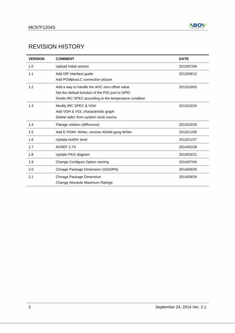
REVISION HISTORY
VERSION COMMENT DATE
1.0 Upload Initial version 2013/07/04
1.1 Add ISP interface guide
Add PGMplusLC connection picture
2013/09/12
1.2 Add a way to handle the ADC zero offset value
Set the default function of the P02 port to GPIO
Divide IRC SPEC according to the temperature condition
2013/10/03
1.3 Modify IRC SPEC & VOH
Add VOH & VOL characteristic graph
Delete wdtrc from system clock source
2013/10/24
1.4 Pakage relation (difference) 2013/10/29
1.5 Add E-PGM+ Writer, remove ADAM gang Writer 2013/11/05
1.6 Updata bod/lvr level 2013/11/27
1.7 AVREF 2.7V 2014/02/28
1.8 Update PKG diagram 2014/03/21
1.9 Change Configure Option naming 2014/07/04
2.0 Chnage Package Dimension (16SOPN) 2014/09/20
2.1 Chnage Package Dimension
Change Absolute Maximum Ratings
2014/09/24
MC97F1204S
September 24, 2014 Ver. 2.1 3
Published by ABOV Semiconductor
2014 ABOV Semiconductor Co., Ltd. All rights reserved.
Additional information of this manual may be served by ABOV Semiconductor offices in Korea or Distributors.
ABOV Semiconductor reserves the right to make changes to any information here in at any time without
notice. The information, diagrams and other data in this manual are correct and reliable;
however, ABOV Semiconductor is in no way responsible for any violations of patents or other rights of the
third party generated by the use of this manual.
MC97F1204S
4 September 24, 2014 Ver. 2.1
Table of Contents REVISION HISTORY .......................................................................................................................................... 2
Table of Contents ................................................................................................................................................. 4
MC97F1204S ....................................................................................................................................................... 8
1. Overview ............................................................................................................................................................ 8
1.1 Description ................................................................................................................................................... 8
1.2 Features ........................................................................................................................................................ 9
1.3 Ordering Information ................................................................................................................................. 10
1.4 Development Tools .................................................................................................................................... 11
2. Block Diagram .................................................................................................................................................. 15
3. Pin Assignment ................................................................................................................................................. 16
4. Package Diagram .............................................................................................................................................. 17
5. Pin Description ................................................................................................................................................. 24
6. Port Structures .................................................................................................................................................. 25
6.1 General Purpose I/O Port ........................................................................................................................... 25
6.2 Second Function I/O Port ........................................................................................................................... 26
6.3 Analog Input I/O Port ................................................................................................................................ 27
6.4 Reset I/O Port............................................................................................................................................. 28
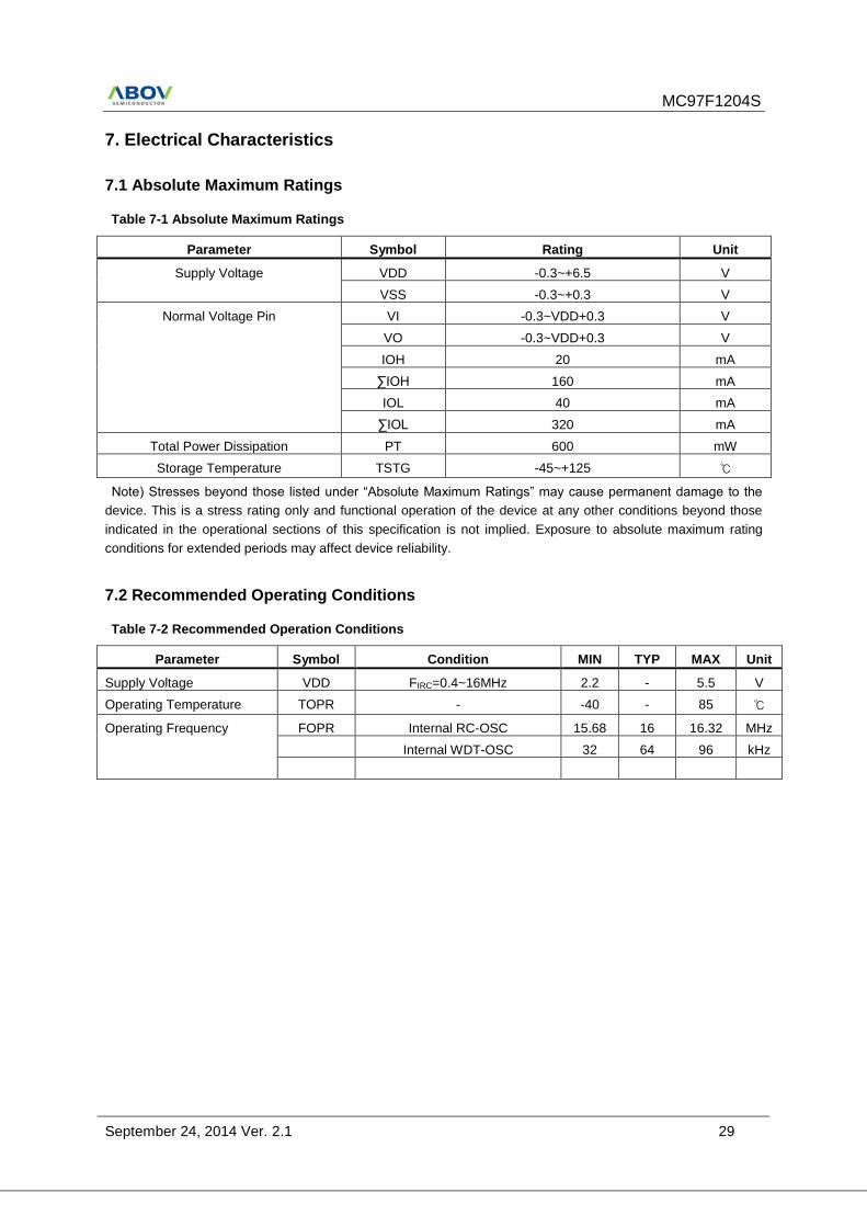
7. Electrical Characteristics .................................................................................................................................. 29
7.1 Absolute Maximum Ratings ...................................................................................................................... 29
7.2 Recommended Operating Conditions ........................................................................................................ 29
7.3 A/D CONVERTER CHARACTERISTICS .............................................................................................. 30
7.4 Voltage Dropout Converter Characteristics ............................................................................................... 30
7.5 Power-On Reset Characteristics ................................................................................................................. 30
7.6 Brown Out Detector Characteristics .......................................................................................................... 31
7.7 Internal RC Oscillator Characteristics ....................................................................................................... 31
7.8 Internal WDT Oscillator Characteristics .................................................................................................... 31
7.9 DC Characteristics ..................................................................................................................................... 32
7.10 AC Characteristics ................................................................................................................................... 33
7.11 SPI Characteristics ................................................................................................................................... 34
7.12 Typical Characteristics ............................................................................................................................. 35
8. Memory ............................................................................................................................................................ 36
8.1 Program Memory ....................................................................................................................................... 36
8.2 Data Memory ............................................................................................................................................. 38
8.3 SFR Map .................................................................................................................................................... 40
9. I/O Ports............................................................................................................................................................ 43
9.1 I/O Ports ..................................................................................................................................................... 43
9.2 PORT P0 .................................................................................................................................................... 44
9.3 PORT P1 .................................................................................................................................................... 45
9.4 PORT P2 .................................................................................................................................................... 47
9.5 PORT SELECT REGISTER PSR0, 2, 3 .................................................................................................... 48
10. Interrupt Controller ......................................................................................................................................... 51
10.1 Overview .................................................................................................................................................. 51
10.2 External Interrupt ..................................................................................................................................... 52
10.3 Block Diagram ......................................................................................................................................... 53
MC97F1204S
September 24, 2014 Ver. 2.1 5
10.4 Interrupt Vector Table .............................................................................................................................. 54
10.5 Interrupt Sequence ................................................................................................................................... 55
10.6 Effective Timing after Controlling Interrupt bit ...................................................................................... 56
10.7 Multi Interrupt .......................................................................................................................................... 57
10.8 Interrupt Enable Accept Timing .............................................................................................................. 58
10.9 Interrupt Service Routine Address ........................................................................................................... 58
10.10 Saving/Restore General-Purpose Registers ............................................................................................ 58
10.11 Interrupt Timing ..................................................................................................................................... 59
10.12 Interrupt Register Description ................................................................................................................ 59
11. Peripheral Hardware ....................................................................................................................................... 66
11.1 Clock Generator ....................................................................................................................................... 66
11.2 BIT ........................................................................................................................................................... 69
11.3 WDT ........................................................................................................................................................ 71
11.4 Timer/PWM ............................................................................................................................................. 74
11.5 SPI............................................................................................................................................................ 83
11.6 12-Bit A/D Converter .............................................................................................................................. 88
12. Power Down Operation .................................................................................................................................. 94
12.1 Overview .................................................................................................................................................. 94
12.2 Peripheral Operation in IDLE/STOP Mode ............................................................................................. 94
12.3 IDLE mode .............................................................................................................................................. 95
12.4 STOP mode .............................................................................................................................................. 96
12.5 Release Operation of STOP1, 2 Mode ..................................................................................................... 97
13. RESET ............................................................................................................................................................ 99
13.1 Overview .................................................................................................................................................. 99
13.2 Reset source ............................................................................................................................................. 99
13.3 Block Diagram ......................................................................................................................................... 99
13.4 RESET Noise Canceller ......................................................................................................................... 100
13.5 Power ON RESET ................................................................................................................................. 100
13.6 External RESETB Input ......................................................................................................................... 103
13.7 Brown Out Detector Processor .............................................................................................................. 104
14. On-chip Debug System ................................................................................................................................. 108
14.1 Overview ................................................................................................................................................ 108
14.2 Two-pin external interface ..................................................................................................................... 109
15. Configure option ........................................................................................................................................... 113
15.1 Configure option Control Register ......................................................................................................... 113
16. APPENDIX .................................................................................................................................................. 114
MC97F1204S
6 September 24, 2014 Ver. 2.1
List of Figures Figure 1-1 On Chip Debugger 2and Pin description (ocd2 mode) ....................................................... 11
Figure 1-2 On Chip Debugger 2 and Pin description (ocd2 mode 1) ................................................... 11
Figure 1-3 Single Programmer ............................................................................................................. 12
Figure 1-4 PGMplusLC Writer ............................................................................................................. 12
Figure 1-5 E-PGM+ Writer................................................................................................................... 13
Figure 1-6 ISP Interface ........................................................................................................................ 14
Figure 2-1 MC97F1204S Block Diagram ............................................................................................. 15
Figure 4-1 20 pin SOP package ............................................................................................................ 17
Figure 4-2 20 pin PDIP package ........................................................................................................... 18
Figure 4-3 20 pin TSSOP package ........................................................................................................ 19
Figure 4-4 16 pin SOP package ............................................................................................................ 20
Figure 4-5 16 pin TSSOP package ........................................................................................................ 21
Figure 4-6 10 pin SSOP package .......................................................................................................... 22
Figure 4-7 8 pin SOP package .............................................................................................................. 23
Figure 6-1 General Purpose I/O Port .................................................................................................... 25
Figure 6-2 Second Function I/O Port .................................................................................................... 26
Figure 6-3 Analog Input I/O Port ......................................................................................................... 27
Figure 6-4 Reset I/O Port ...................................................................................................................... 28
Figure 7-1 AC Timing .......................................................................................................................... 33
Figure 7-2 SPI Timing .......................................................................................................................... 34
Figure 7-3 Output High Voltage (VOH) ............................................................................................... 35
Figure 7-4 Output Low Voltage (VOL) ................................................................................................ 35
Figure 8-1 Program Memory ................................................................................................................ 37
Figure 8-2 Data Memory map .............................................................................................................. 38
Figure 8-3 Low 128bytes RAM ............................................................................................................ 39
Figure 10-1 Interrupt Priority Level ..................................................................................................... 51
Figure 10-2 External Interrupt Description ........................................................................................... 52
Figure 10-3 Block Diagram of Interrupt ............................................................................................... 53
Figure 10-4 Interrupt Execution Sequence ........................................................................................... 55
Figure 10-5 Interrupt Enable Register effective Timing ....................................................................... 56
Figure 10-6 Execution of Multi Interrupt ............................................................................................. 57
Figure 10-7 Interrupt Response Timing Diagram ................................................................................. 58
Figure 10-8 Correspondence between vector table address and the entry address of ISR .................... 58
Figure 10-9 Saving/Restore Process Diagram & Sample Source ......................................................... 58
Figure 10-10 Timing chart of Interrupt Acceptance and Interrupt Return Instruction .......................... 59
Figure 11-1 Clock Generator Block Diagram ....................................................................................... 66
Figure 11-2 BIT Block Diagram ........................................................................................................... 69
Figure 11-3 WDT Block Diagram ........................................................................................................ 71
Figure 11-4 WDT Interrupt Timing Waveform .................................................................................... 73
Figure 11-5 Timer x 16-bit Mode Block Diagram ................................................................................ 74
Figure 11-6 Timer x 16bit Capture Mode ............................................................................................. 75
MC97F1204S
September 24, 2014 Ver. 2.1 7
Figure 11-7 PWM Mode ....................................................................................................................... 76
Figure 11-8 Example of PWM at 8MHz ............................................................................................... 77
Figure 11-9 Example of PWM at 8MHz (Period = Duty) .................................................................... 77
Figure 11-10 SPI Block Diagram ......................................................................................................... 83
Figure 11-11 SPI Transmit/Receive Timing Diagram at CPHA = 0 .................................................... 85
Figure 11-12 SPI Transmit/Receive Timing Diagram at CPHA = 1 .................................................... 85
Figure 11-13 ADC Block Diagram ....................................................................................................... 89
Figure 11-14 A/D Analog Input Pin Connecting Capacitor .................................................................. 89
Figure 11-15 A/D Power(AVDD) Pin Connecting Capacitor .............................................................. 89
Figure 11-16 ADC Operation for Align bit .......................................................................................... 90
Figure 11-17 Converter Operation Flow ............................................................................................... 91
Figure 12-1 IDLE Mode Release Timing by External Interrupt ........................................................... 95
Figure 12-2 IDLE Mode Release Timing by /RESET .......................................................................... 95
Figure 12-3 STOP Mode Release Timing by External Interrupt .......................................................... 96
Figure 12-4 STOP Mode Release Timing by /RESET ......................................................................... 96
Figure 12-5 STOP1, 2 Mode Release Flow .......................................................................................... 97
Figure 13-1 RESET Block Diagram ..................................................................................................... 99
Figure 13-2 Reset noise canceller time diagram ................................................................................. 100
Figure 13-3 Fast VDD rising time ...................................................................................................... 100
Figure 13-4 Internal RESET Release Timing On Power-Up .............................................................. 101
Figure 13-5 Configuration timing when Power-on (at 8Mhz) ............................................................ 101
Figure 13-6 Boot Process Wave Form ................................................................................................ 102
Figure 13-7 Timing Diagram after RESET......................................................................................... 103
Figure 13-8 Oscillator generating waveform example ........................................................................ 103
Figure 13-9 Block Diagram of BOD .................................................................................................. 104
Figure 13-10 Internal Reset at the power fail situation ....................................................................... 104
Figure 13-11 Configuration timing when BOD RESET ..................................................................... 105
Figure 14-1 Block Diagram of On-chip Debug System ...................................................................... 109
Figure 14-2 10-bit transmission packet ............................................................................................... 110
Figure 14-3 Data transfer on the twin bus........................................................................................... 110
Figure 14-4 Bit transfer on the serial bus ............................................................................................ 111
Figure 14-5 Start and stop condition ................................................................................................... 111
Figure 14-6 Acknowledge on the serial bus........................................................................................ 111
Figure 14-7 Clock synchronization during wait procedure ................................................................. 112
Figure 14-8 Connection of transmission ............................................................................................. 112
MC97F1204S
8 September 24, 2014 Ver. 2.1
MC97F1204S
CMOS SINGLE-CHIP 8-BIT MICROCONTROLLER WITH 12-BIT ANALOG TO DIGITAL CONVERTER
1. Overview
1.1 Description
The MC97F1204Sis an advanced CMOS 8-bit microcontroller with 4Kbytes of FLASH. This is
powerful microcontroller which provides a highly flexible and cost effective solution to many
embedded control applications. This provides the following features :4Kbytes of FLASH, 256bytes of
IRAM, 16-bit timer/counter, Watchdog timer with WDTOSC, 12-bit ADC, SPI, On-chip POR, BOD and
LVR, 16-bit PWM output, Internal RC-Oscillator, Internal WDT-Oscillator and clock circuitry. The
MC97F1204S also supports Power saving modes to reduce Power Consumption.
Device Name FLASH RAM Package
MC97F1204S
MC97F1104S 4Kbytes SRAM : 256bytes 20/16/10/8 pins
MC97F1204S
September 24, 2014 Ver. 2.1 9
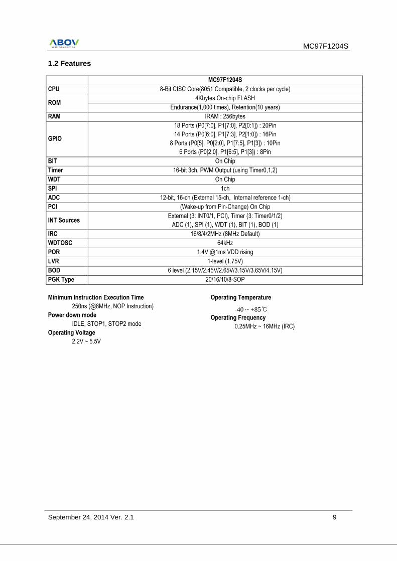
1.2 Features
MC97F1204S
CPU 8-Bit CISC Core(8051 Compatible, 2 clocks per cycle)
ROM 4Kbytes On-chip FLASH
Endurance(1,000 times), Retention(10 years)
RAM IRAM : 256bytes
GPIO
18 Ports (P0[7:0], P1[7:0], P2[0:1]) : 20Pin
14 Ports (P0[6:0], P1[7:3], P2[1:0]) : 16Pin
8 Ports (P0[5], P0[2:0], P1[7:5], P1[3]) : 10Pin
6 Ports (P0[2:0], P1[6:5], P1[3]) : 8Pin
BIT On Chip
Timer 16-bit 3ch, PWM Output (using Timer0,1,2)
WDT On Chip
SPI 1ch
ADC 12-bit, 16-ch (External 15-ch, Internal reference 1-ch)
PCI (Wake-up from Pin-Change) On Chip
INT Sources External (3: INT0/1, PCI), Timer (3: Timer0/1/2)
ADC (1), SPI (1), WDT (1), BIT (1), BOD (1)
IRC 16/8/4/2MHz (8MHz Default)
WDTOSC 64kHz
POR 1.4V @1ms VDD rising
LVR 1-level (1.75V)
BOD 6 level (2.15V/2.45V/2.65V/3.15V/3.65V/4.15V)
PGK Type 20/16/10/8-SOP
Minimum Instruction Execution Time
250ns (@8MHz, NOP Instruction)
Power down mode
IDLE, STOP1, STOP2 mode
Operating Voltage
2.2V ~ 5.5V
Operating Temperature
-40 ~ +85℃
Operating Frequency
0.25MHz ~ 16MHz (IRC)
MC97F1204S
10 September 24, 2014 Ver. 2.1
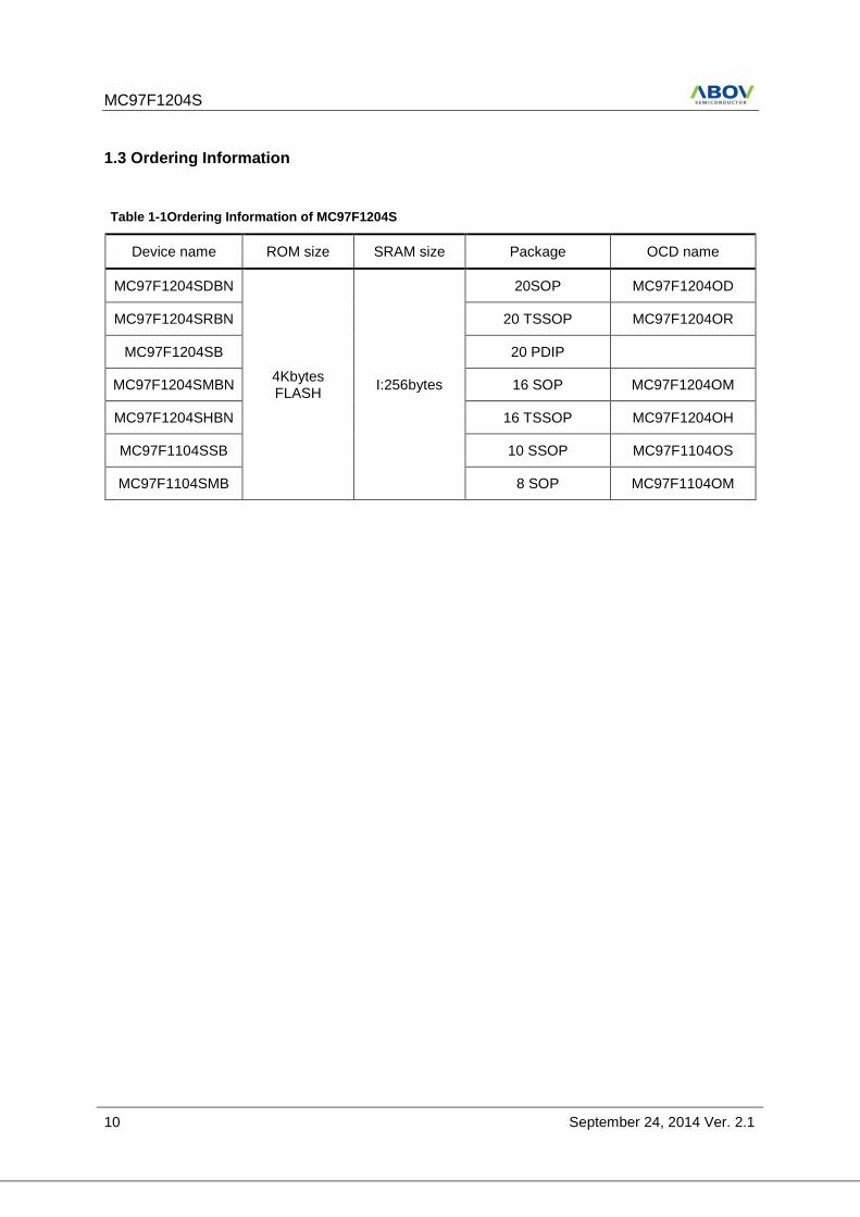
1.3 Ordering Information
Table 1-1Ordering Information of MC97F1204S
Device name ROM size SRAM size Package OCD name
MC97F1204SDBN
4Kbytes FLASH
I:256bytes
20SOP MC97F1204OD
MC97F1204SRBN 20 TSSOP MC97F1204OR
MC97F1204SB 20 PDIP
MC97F1204SMBN 16 SOP MC97F1204OM
MC97F1204SHBN 16 TSSOP MC97F1204OH
MC97F1104SSB 10 SSOP MC97F1104OS
MC97F1104SMB 8 SOP MC97F1104OM
MC97F1204S
September 24, 2014 Ver. 2.1 11
1.4 Development Tools
1.4.1 Compiler
We do not provide the compiler. Please contact third parties.
The MC97F1204S core is Mentor Graphic 8051.Anyway,device ROM size is smaller than
64Kbytes.Developer can use all kinds of third party’s standard 8051 compiler.
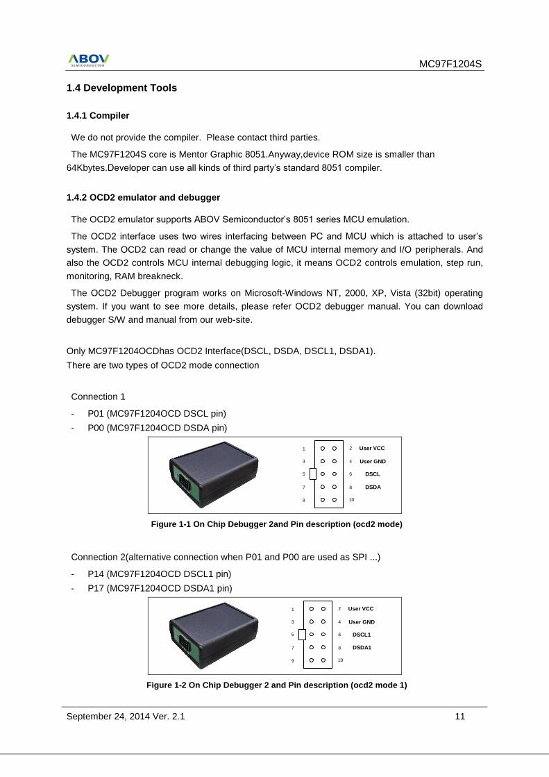
1.4.2 OCD2 emulator and debugger
The OCD2 emulator supports ABOV Semiconductor’s 8051 series MCU emulation.
The OCD2 interface uses two wires interfacing between PC and MCU which is attached to user’s
system. The OCD2 can read or change the value of MCU internal memory and I/O peripherals. And
also the OCD2 controls MCU internal debugging logic, it means OCD2 controls emulation, step run,
monitoring, RAM breakneck.
The OCD2 Debugger program works on Microsoft-Windows NT, 2000, XP, Vista (32bit) operating
system. If you want to see more details, please refer OCD2 debugger manual. You can download
debugger S/W and manual from our web-site.
Only MC97F1204OCDhas OCD2 Interface(DSCL, DSDA, DSCL1, DSDA1).
There are two types of OCD2 mode connection
Connection 1
- P01 (MC97F1204OCD DSCL pin)
- P00 (MC97F1204OCD DSDA pin)
Figure 1-1 On Chip Debugger 2and Pin description (ocd2 mode)
Connection 2(alternative connection when P01 and P00 are used as SPI ...)
- P14 (MC97F1204OCD DSCL1 pin)
- P17 (MC97F1204OCD DSDA1 pin)
Figure 1-2 On Chip Debugger 2 and Pin description (ocd2 mode 1)
2
2
2 User VCC 1
3 4
5 6
7 8
10 9
User GND
DSCL1
DSDA1
2 User VCC 1
3 4
5 6
7 8
10 9
User GND
DSCL
DSDA
MC97F1204S
12 September 24, 2014 Ver. 2.1
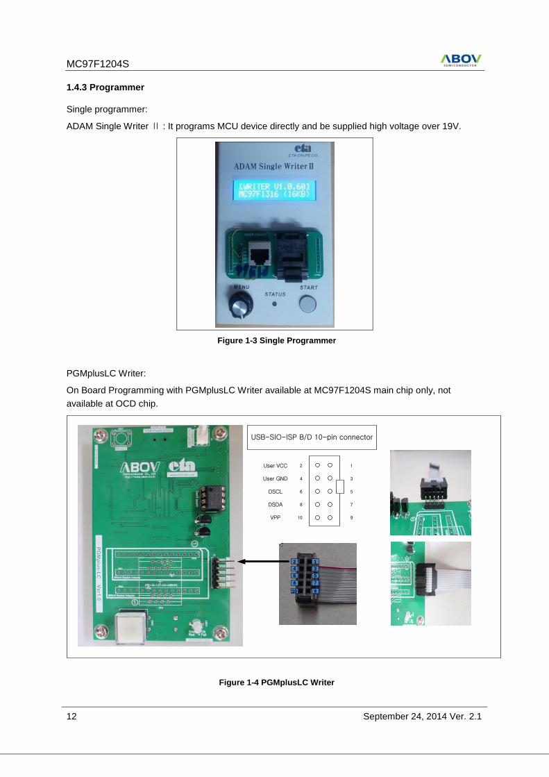
1.4.3 Programmer
Single programmer:
ADAM Single Writer Ⅱ : It programs MCU device directly and be supplied high voltage over 19V.
Figure 1-3 Single Programmer
PGMplusLC Writer:
On Board Programming with PGMplusLC Writer available at MC97F1204S main chip only, not
available at OCD chip.
2
4
6
8
10
1
3
5
7
9
USB-SIO-ISP B/D 10-pin connector
User VCC
User GND
DSCL
DSDA
VPP
2
4
6
8
10
1
3
5
7
9
Figure 1-4 PGMplusLC Writer
MC97F1204S
September 24, 2014 Ver. 2.1 13
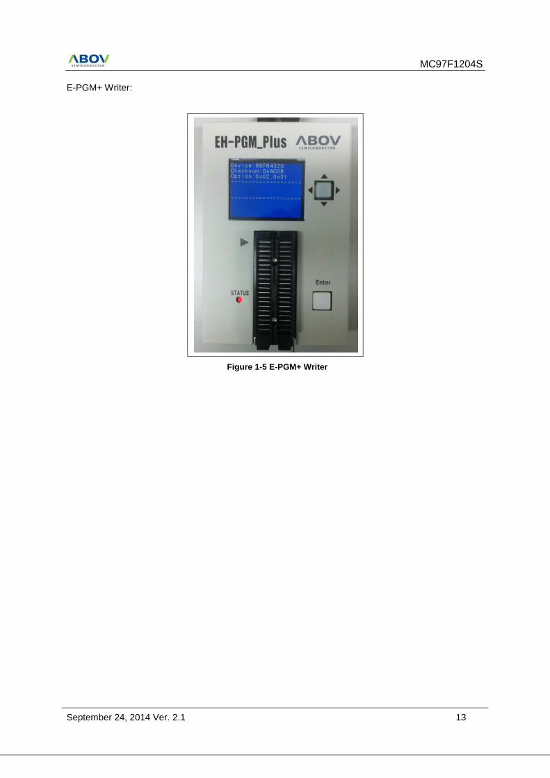
E-PGM+ Writer:
Figure 1-5 E-PGM+ Writer
MC97F1204S
14 September 24, 2014 Ver. 2.1
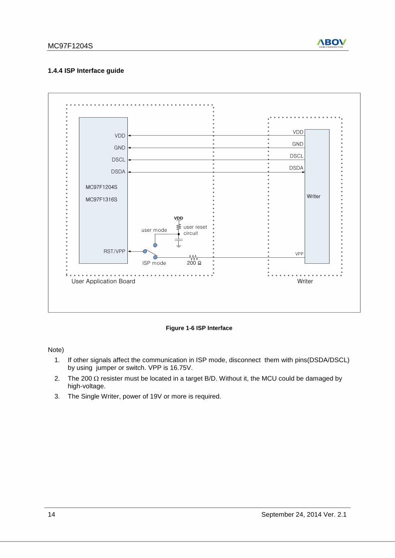
1.4.4 ISP Interface guide
MC97F1204S
MC97F1316S
VDD
GND
DSCL
DSDA
Writer
VDD
VDD
GND
DSCL
DSDA
VPP
user mode
ISP mode
user resetcircuit
User Application Board Writer
200 Ω
RST/VPP
Figure 1-6 ISP Interface
Note)
1. If other signals affect the communication in ISP mode, disconnect them with pins(DSDA/DSCL) by using jumper or switch. VPP is 16.75V.
2. The 200 resister must be located in a target B/D. Without it, the MCU could be damaged by high-voltage.
3. The Single Writer, power of 19V or more is required.
MC97F1204S
September 24, 2014 Ver. 2.1 15
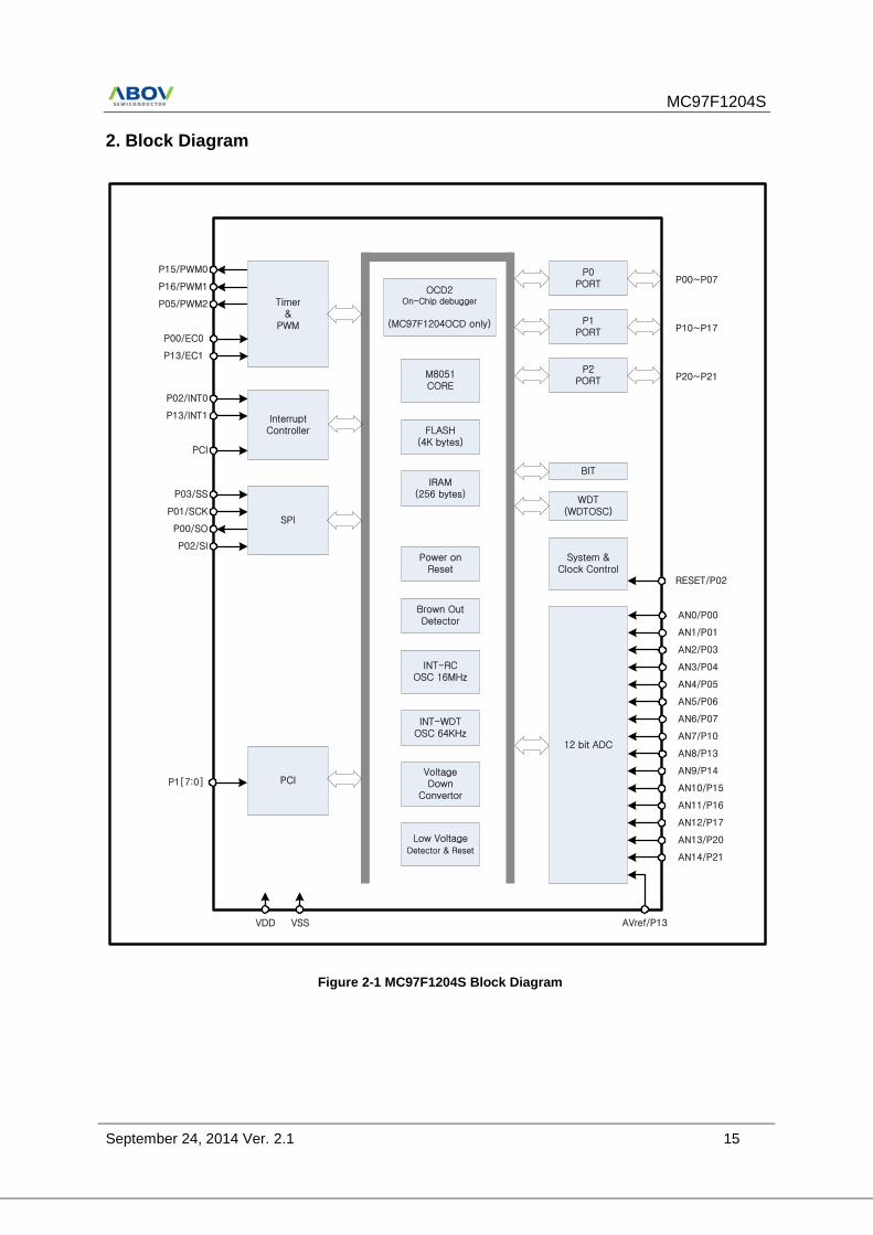
2. Block Diagram
Timer&
PWM
InterruptController
SPI
12 bit ADC
OCD2On-Chip debugger
(MC97F1204OCD only)
M8051CORE
FLASH(4K bytes)
Power onReset
Brown OutDetector
INT-RCOSC 16MHz
INT-WDTOSC 64KHz
VoltageDown
Convertor
Low VoltageDetector & Reset
P0PORT
P1PORT
P2PORT
BIT
WDT(WDTOSC)
System &Clock Control
IRAM(256 bytes)
P15/PWM0
P16/PWM1
P05/PWM2
P02/INT0
P13/INT1
PCI
P03/SS
P01/SCK
P00/SO
P02/SI
AN9/P14
AN10/P15
AN11/P16
AN12/P17
AN13/P20
AN14/P21
RESET/P02
P00~P07
P10~P17
P20~P21
AN0/P00
AN1/P01
AN2/P03
AN3/P04
AN4/P05
AN5/P06
AN6/P07
AN7/P10
AN8/P13
VDD VSS AVref/P13
PCIP1[7:0]
P00/EC0
P13/EC1
Figure 2-1 MC97F1204S Block Diagram
MC97F1204S
16 September 24, 2014 Ver. 2.1
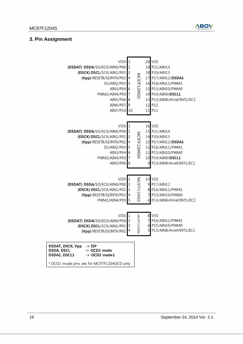
3. Pin Assignment
MC97F1
104SS
MC97F1204SM
MC97F1204SD
MC97F1104SM
VDD 1 8 VSS
2 7 P16/AIN11/PWM1
3 6 P15/AIN10/PWM0
4 5 P13/AIN8/Avref/INT1/EC1
(DSDAT) DSDA/SO/EC0/AIN0/P00
(DSCK) DSCL/SCK/AIN1/P01
(Vpp) RESETB/SI/INT0/P02
VDD 1 10 VSS
2 9 P17/AIN12
3 8 P16/AIN11/PWM1
4 7 P15/AIN10/PWM0
PWM2/AIN4/P05 5 6 P13/AIN8/AVref/INT1/EC1
(DSDAT) DSDA/SO/EC0/AIN0/P00
(DSCK) DSCL/SCK/AIN1/P01
(Vpp) RESETB/SI/INT0/P02
VDD 1 16 VSS
2 15 P21/AIN14
3 14 P20/AIN13
4 13 P17/AIN12/DSDA1
SS/AIN2/P03 5 12 P16/AIN11/PWM1
AIN3/P04 6 11 P15/AIN10/PWM0
PWM2/AIN4/P05 7 10 P14/AIN9/DSCL1
AIN5/P06 8 9 P13/AIN8/Avref/INT1/EC1
(DSDAT) DSDA/SO/EC0/AIN0/P00
(DSCK) DSCL/SCK/AIN1/P01
(Vpp) RESETB/SI/INT0/P02
VDD 1 20 VSS
(DSDAT) DSDA/SO/EC0/AIN0/P00 2 19 P21/AIN14
3 18 P20/AIN13
4 17 P17/AIN12/DSDA1
SS/AIN2/P03 5 16 P16/AIN11/PWM1
AIN3/P04 6 15 P15/AIN10/PWM0
PWM2/AIN4/P05 7 14 P14/AIN9/DSCL1
AIN5/P06 8 13 P13/AIN8/AVref/INT1/EC1
AIN6/P07 9 12 P12
AIN7/P10 10 11 P11
(DSCK) DSCL/SCK/AIN1/P01
(Vpp) RESETB/SI/INT0/P02
DSDAT, DSCK, Vpp -> ISPDSDA, DSCL -> OCD2 modeDSDA1, DSCL1 -> OCD2 mode1
* OCD2 mode pins are for MC97F1204OCD only
MC97F1204S
September 24, 2014 Ver. 2.1 17
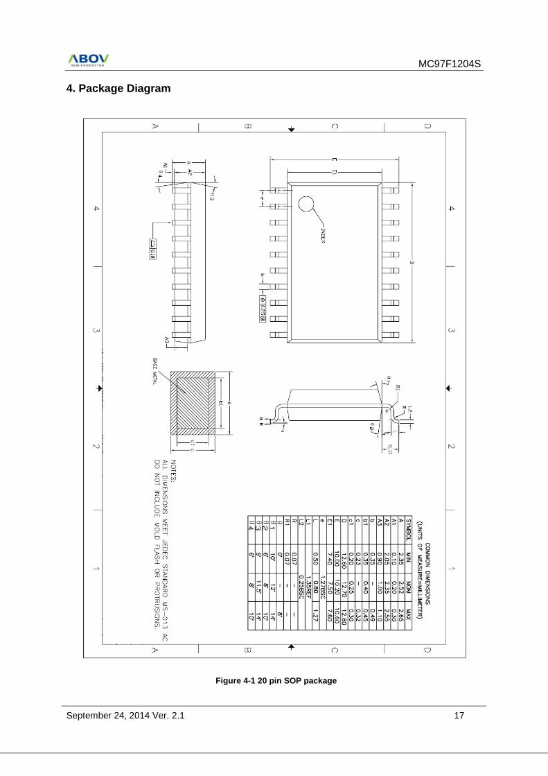
4. Package Diagram
Figure 4-1 20 pin SOP package
MC97F1204S
18 September 24, 2014 Ver. 2.1
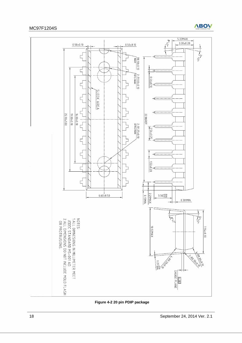
Figure 4-2 20 pin PDIP package
MC97F1204S
September 24, 2014 Ver. 2.1 19
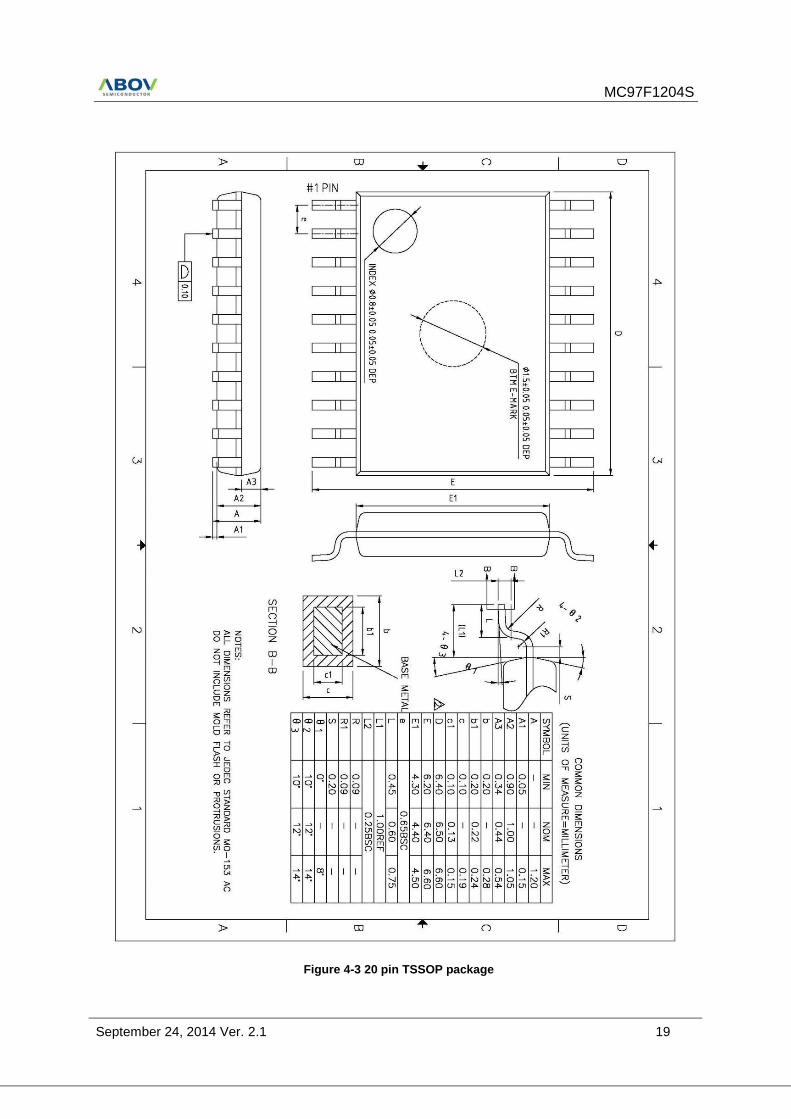
Figure 4-3 20 pin TSSOP package
MC97F1204S
20 September 24, 2014 Ver. 2.1
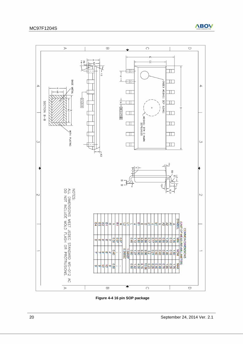
Figure 4-4 16 pin SOP package
MC97F1204S
September 24, 2014 Ver. 2.1 21
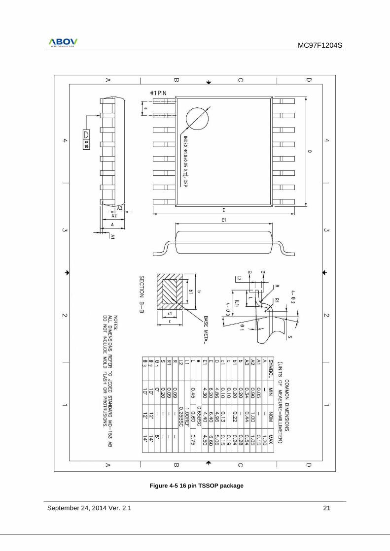
Figure 4-5 16 pin TSSOP package
MC97F1204S
22 September 24, 2014 Ver. 2.1
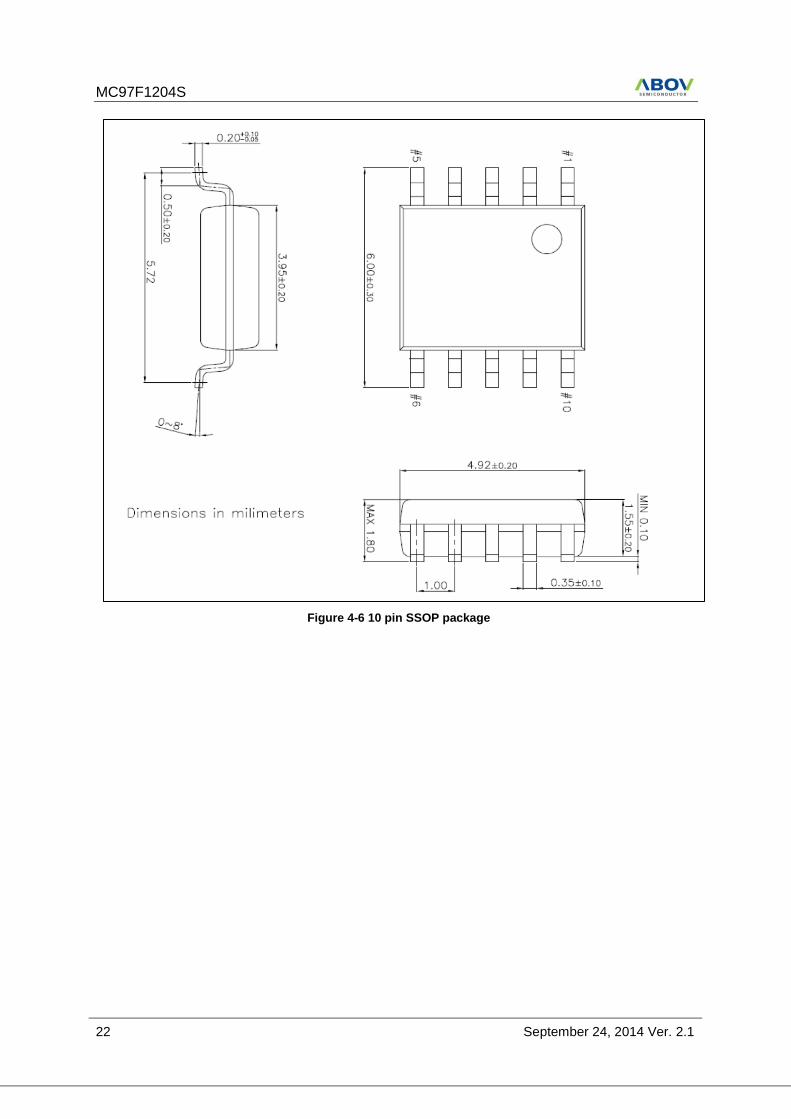
Figure 4-6 10 pin SSOP package

MC97F1204S
September 24, 2014 Ver. 2.1 23
Figure 4-7 8 pin SOP package
MC97F1204S
24 September 24, 2014 Ver. 2.1
5. Pin Description
Table 5-1 Normal Pin description
PIN Name
I/O Function @RESET Shared with
P00
I/O
Port P0 8-Bit I/O Port Can be set in input or output mode in 1-bit units Internal pull-up register can be used via software when this port is used as input port Open Drain enable register can be used via software when this port is used as output port (P02 OpenDrain output only)
Input
AIN0 / EC0 / SO / (DSDA)
P01 AIN1 / SCK / (DSCL)
P02 INT0 / SI / RESETB / (Vpp)
P03 AIN2 / SS
P04 AIN3
P05 AIN4 / PWM2
P06 AIN5
P07 AIN6
P10
I/O
Port P1 8-Bit I/O Port Can be set in input or output mode in 1-bit units Internal pull-up register can be used via software when this port is used as input port Open Drain enable register can be used via software when this port is used as output port
Input
AIN7
P11 -
P12 -
P13 AIN8 / Averf / INT1 / EC1
P14 AIN9 / (DSCL1)
P15 AIN10 / PWM0
P16 AIN11 / PWM1
P17 AIN12 / (DSDA1)
P20
I/O
Port P2 2bit I/O Port Can be set in input or output mode in 1-bit units Internal pull-up register can be used via software when this port is used as input port Open Drain enable register can be used via software when this port is used as output port
Input
AIN13
P21 AIN14
-
-
-
-
MC97F1204S
September 24, 2014 Ver. 2.1 25
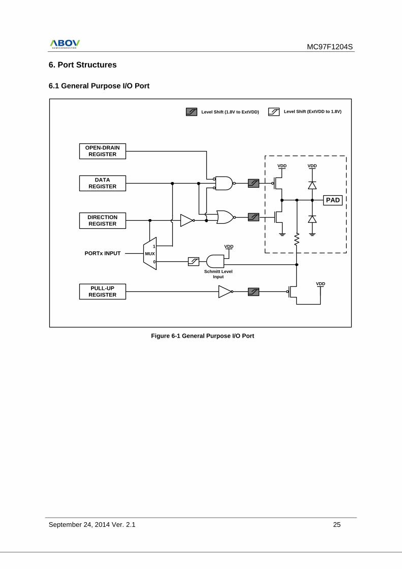
6. Port Structures
6.1 General Purpose I/O Port
DATA
REGISTER
DIRECTION
REGISTER
PORTx INPUT
PAD
VDDVDD
Schmitt Level
Input
Level Shift (1.8V to ExtVDD) Level Shift (ExtVDD to 1.8V)
VDD
MUX
1
0
PULL-UP
REGISTER
VDD
OPEN-DRAIN
REGISTER
Figure 6-1 General Purpose I/O Port
MC97F1204S
26 September 24, 2014 Ver. 2.1
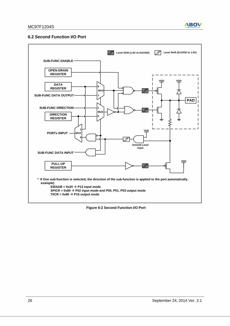
6.2 Second Function I/O Port
DATA
REGISTER
SUB-FUNC DATA OUTPUT
SUB-FUNC ENABLE
DIRECTION
REGISTER
SUB-FUNC DIRECTION
SUB-FUNC DATA INPUT
PORTx INPUT
PAD
VDDVDD
MUX
MUX
0
1
MUX
1
0
0
1
Schmitt Level
Input
VDD
Level Shift (1.8V to ExtVDD) Level Shift (ExtVDD to 1.8V)
OPEN-DRAIN
REGISTER
PULL-UP
REGISTER
VDD
* If One sub-function is selected, the direction of the sub-function is applied to the port automatically.
example)
EIENAB = 0x20 à P13 input mode
SPICR = 0x80 à P02 input mode and P00, P01, P03 output mode
T0CR = 0x80 à P15 output mode
Figure 6-2 Second Function I/O Port
MC97F1204S
September 24, 2014 Ver. 2.1 27
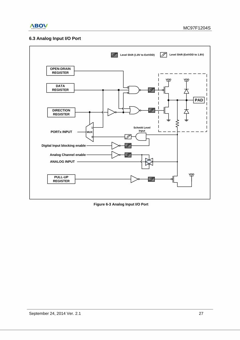
6.3 Analog Input I/O Port
DATA
REGISTER
DIRECTION
REGISTER
PORTx INPUT
PAD
VDDVDD
Schmitt Level
Input
Level Shift (1.8V to ExtVDD) Level Shift (ExtVDD to 1.8V)
MUX
1
0
Analog Channel enable
ANALOG INPUT
Digital Input blocking enable
OPEN-DRAIN
REGISTER
PULL-UP
REGISTER
VDD
Figure 6-3 Analog Input I/O Port
MC97F1204S
28 September 24, 2014 Ver. 2.1
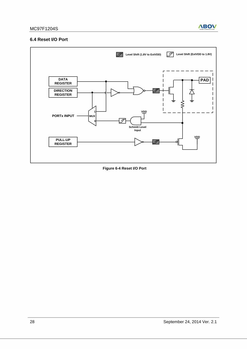
6.4 Reset I/O Port
DATA
REGISTER
DIRECTION
REGISTER
PORTx INPUT
PAD
Schmitt Level
Input
Level Shift (1.8V to ExtVDD) Level Shift (ExtVDD to 1.8V)
VDD
MUX
1
0
PULL-UP
REGISTER
VDD
Figure 6-4 Reset I/O Port
MC97F1204S
September 24, 2014 Ver. 2.1 29
7. Electrical Characteristics
7.1 Absolute Maximum Ratings
Table 7-1 Absolute Maximum Ratings
Parameter Symbol Rating Unit
Supply Voltage VDD -0.3~+6.5 V
VSS -0.3~+0.3 V
Normal Voltage Pin VI -0.3~VDD+0.3 V
VO -0.3~VDD+0.3 V
IOH 20 mA
∑IOH 160 mA
IOL 40 mA
∑IOL 320 mA
Total Power Dissipation PT 600 mW
Storage Temperature TSTG -45~+125 ℃
Note) Stresses beyond those listed under “Absolute Maximum Ratings” may cause permanent damage to the
device. This is a stress rating only and functional operation of the device at any other conditions beyond those
indicated in the operational sections of this specification is not implied. Exposure to absolute maximum rating
conditions for extended periods may affect device reliability.
7.2 Recommended Operating Conditions
Table 7-2 Recommended Operation Conditions
Parameter Symbol Condition MIN TYP MAX Unit
Supply Voltage VDD FIRC=0.4~16MHz 2.2 - 5.5 V
Operating Temperature TOPR - -40 - 85 ℃
Operating Frequency FOPR Internal RC-OSC 15.68 16 16.32 MHz
Internal WDT-OSC 32 64 96 kHz
MC97F1204S
30 September 24, 2014 Ver. 2.1
Note) -STOP1: WDTRC running- STOP2: WDTRC disable
7.3 A/D CONVERTER CHARACTERISTICS
(TA = - 40C to + 85C, VDD = 2.7– 5.5V, Vss=0V)
Parameter Symbol Conditions Min Typ Max Units
Resolution – – – 12 – bit
Integral Linear Error INL AVREF=2.7V – 5.5V,
fx=8MHz
– – ±4 LSB
Differential Linearity Error
DLE – – ±1
Zero Offset Error ZOE -3 – +7
Full Scale Error FSE – – ±3
Conversion Time tCON 12bit resolution, fx=8MHz 20 – – us
Analog Input Voltage VAN – VSS – AVREF V
Analog Reference Voltage AVREF – 2.7NOTE
– VDD
VDD18 – – – 1.8 – V
A/DC Input Leakage Current IAN - – – 2 uA
ADC Current IADC Enable VDD=5.12V – 1 2 mA
Disable – – 0.1 uA
Notes: 1. Zero offset error is the difference between 000000000000 and the converted output for zero input voltage (VSS); 2. Full scale error is the difference between 111111111111 and the converted output for full-scale input voltage (VDD).
3. ADC zero offset value(-3LSB ~ 7 LSB) is addressed at 0x4007 of option memory.
4. Under 2.7V, the ADC resolution decrease.
7.4 Voltage Dropout Converter Characteristics
Table 7-3 Voltage Dropout Converter Characteristics
Parameter Symbol Condition MIN TYP MAX Unit
Operating Voltage - 2.2 - 5.5 V
Operating Temperature - -40 - +85 ℃
Regulation Voltage - 1.62 1.8 1.98 V
Current Drivability - - 20 - mA
Operating Current IDD1 RUN/IDLE - 0.5 mA
TRAN STOP to RUN - 200 us
STOP1 - 0.5 - uA
STOP2 - 0.5 - uA
7.5 Power-On Reset Characteristics
Table 7-4 Power-On Reset Characteristics
Parameter Symbol Condition MIN TYP MAX Unit
Operating Voltage - VSS - 5.5 V
Operating Temperature - -40 - +85 ℃
RESET Release Level - 1.2 1.4 1.6 V
Operating Current IDD - - 0.1 - uA
MC97F1204S
September 24, 2014 Ver. 2.1 31
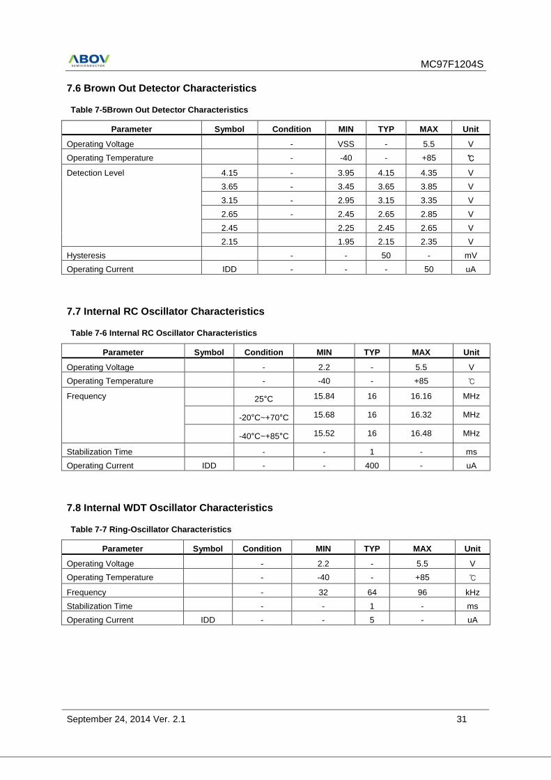
7.6 Brown Out Detector Characteristics
Table 7-5Brown Out Detector Characteristics
Parameter Symbol Condition MIN TYP MAX Unit
Operating Voltage - VSS - 5.5 V
Operating Temperature - -40 - +85 ℃
Detection Level 4.15 - 3.95 4.15 4.35 V
3.65 - 3.45 3.65 3.85 V
3.15 - 2.95 3.15 3.35 V
2.65 - 2.45 2.65 2.85 V
2.45 2.25 2.45 2.65 V
2.15 1.95 2.15 2.35 V
Hysteresis - - 50 - mV
Operating Current IDD - - - 50 uA
7.7 Internal RC Oscillator Characteristics
Table 7-6 Internal RC Oscillator Characteristics
Parameter Symbol Condition MIN TYP MAX Unit
Operating Voltage - 2.2 - 5.5 V
Operating Temperature - -40 - +85 ℃
Frequency 25°C 15.84 16 16.16 MHz
-20°C~+70°C 15.68 16 16.32 MHz
-40°C~+85°C 15.52 16 16.48 MHz
Stabilization Time - - 1 - ms
Operating Current IDD - - 400 - uA
7.8 Internal WDT Oscillator Characteristics
Table 7-7 Ring-Oscillator Characteristics
Parameter Symbol Condition MIN TYP MAX Unit
Operating Voltage - 2.2 - 5.5 V
Operating Temperature - -40 - +85 ℃
Frequency - 32 64 96 kHz
Stabilization Time - - 1 - ms
Operating Current IDD - - 5 - uA
MC97F1204S
32 September 24, 2014 Ver. 2.1
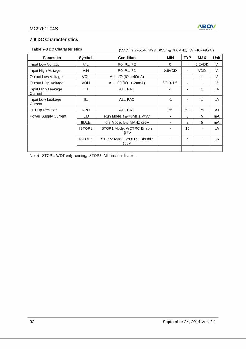
(VDD =2.2~5.5V, VSS =0V, fIRC=8.0MHz, TA=-40~+85℃)
7.9 DC Characteristics
Table 7-8 DC Characteristics
Parameter Symbol Condition MIN TYP MAX Unit
Input Low Voltage VIL P0, P1, P2 0 - 0.2VDD V
Input High Voltage VIH P0, P1, P2 0.8VDD - VDD V
Output Low Voltage VOL ALL I/O (IOL=40mA) - - 1 V
Output High Voltage VOH ALL I/O (IOH=-20mA) VDD-1.5 - - V
Input High Leakage Current
IIH ALL PAD -1 - 1 uA
Input Low Leakage Current
IIL ALL PAD -1 - 1 uA
Pull-Up Resister RPU ALL PAD 25 50 75 kΩ
Power Supply Current IDD Run Mode, fXIN=8MHz @5V - 3 5 mA
IIDLE Idle Mode, fXIN=8MHz @5V - 2 5 mA
ISTOP1 STOP1 Mode, WDTRC Enable @5V
- 10 - uA
ISTOP2 STOP2 Mode, WDTRC Disable @5V
- 5 - uA
Note) STOP1: WDT only running, STOP2: All function disable.
MC97F1204S
September 24, 2014 Ver. 2.1 33
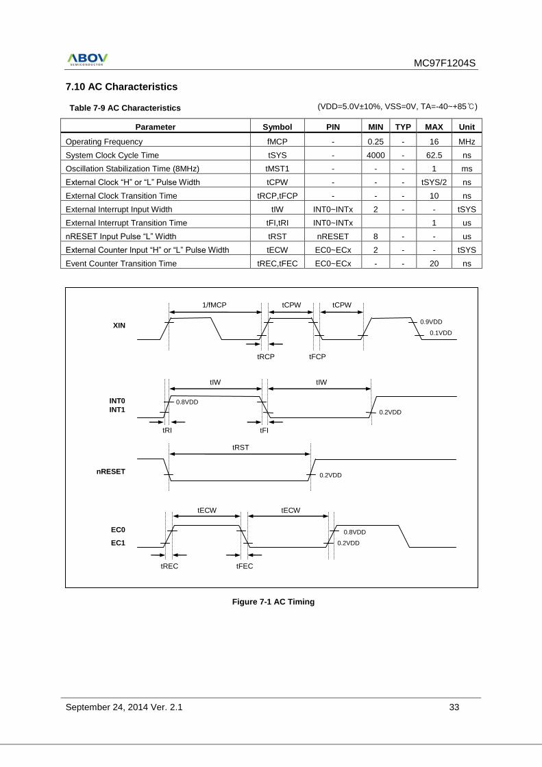
7.10 AC Characteristics
Table 7-9 AC Characteristics
Parameter Symbol PIN MIN TYP MAX Unit
Operating Frequency fMCP - 0.25 - 16 MHz
System Clock Cycle Time tSYS - 4000 - 62.5 ns
Oscillation Stabilization Time (8MHz) tMST1 - - - 1 ms
External Clock “H” or “L” Pulse Width tCPW - - - tSYS/2 ns
External Clock Transition Time tRCP,tFCP - - - 10 ns
External Interrupt Input Width tIW INT0~INTx 2 - - tSYS
External Interrupt Transition Time tFI,tRI INT0~INTx 1 us
nRESET Input Pulse “L” Width tRST nRESET 8 - - us
External Counter Input “H” or “L” Pulse Width tECW EC0~ECx 2 - - tSYS
Event Counter Transition Time tREC,tFEC EC0~ECx - - 20 ns
(VDD=5.0V±10%, VSS=0V, TA=-40~+85℃)
Figure 7-1 AC Timing
XIN 0.9VDD
0.1VDD
1/fMCP tCPW tCPW
tRCP tFCP
EC0
0.8VDD
0.2VDD
tIW tIW
tRST
0.2VDD
0.8VDD
0.2VDD
tECW tECW
INT0
INT1
nRESET
tREC tFEC
EC1
tFI tRI
MC97F1204S
34 September 24, 2014 Ver. 2.1
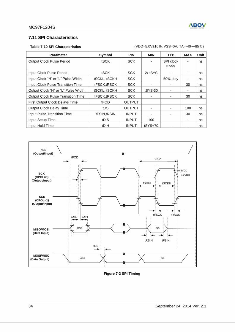
7.11 SPI Characteristics
Table 7-10 SPI Characteristics
Parameter Symbol PIN MIN TYP MAX Unit
Output Clock Pulse Period tSCK SCK - SPI clock mode
- ns
Input Clock Pulse Period tSCK SCK 2 tSYS - - ns
Input Clock “H” or “L” Pulse Width tSCKL, tSCKH SCK 50% duty - ns
Input Clock Pulse Transition Time tFSCK,tRSCK SCK - - 30 ns
Output Clock “H” or “L” Pulse Width tSCKL, tSCKH SCK tSYS-30 - - ns
Output Clock Pulse Transition Time tFSCK,tRSCK SCK - - 30 ns
First Output Clock Delays Time tFOD OUTPUT
Output Clock Delay Time tDS OUTPUT - - 100 ns
Input Pulse Transition Time tFSIN,tRSIN INPUT - - 30 ns
Input Setup Time tDIS INPUT 100 - ns
Input Hold Time tDIH INPUT tSYS+70 - - ns
SCK (CPOL=1)
(Output/Input)
MOSI/MISO
(Data Output)
MISO/MOSI
(Data Input)
tSCK
tRSIN
0.8VDD
0.2VDD
tDS
SCK (CPOL=0)
(Output/Input) tSCKH tSCKL
/SS
(Output/Input)
MSB LSB
LSB MSB
tDIS tDIH tFSCK tRSCK
tFSIN
tFOD
(VDD=5.0V±10%, VSS=0V, TA=-40~+85℃)
Figure 7-2 SPI Timing
MC97F1204S
September 24, 2014 Ver. 2.1 35
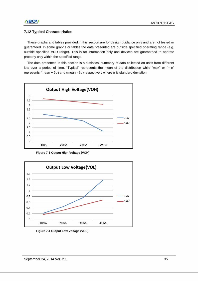
7.12 Typical Characteristics
These graphs and tables provided in this section are for design guidance only and are not tested or
guaranteed. In some graphs or tables the data presented are outside specified operating range (e.g.
outside specified VDD range). This is for information only and devices are guaranteed to operate
properly only within the specified range.
The data presented in this section is a statistical summary of data collected on units from different
lots over a period of time. “Typical” represents the mean of the distribution while “max” or “min”
represents (mean + 3σ) and (mean - 3σ) respectively where σ is standard deviation.
Figure 7-3 Output High Voltage (VOH)
Figure 7-4 Output Low Voltage (VOL)
MC97F1204S
36 September 24, 2014 Ver. 2.1
8. Memory
The MC97F1204S addresses two separate address memory stores: Program memory and Data
memory. The logical separation of Program and Data memory allows Data memory to be accessed by
8-bit addresses, which can be more quickly stored and manipulated by 8-bit CPU.
Program memory can only be read, not written to providing up to 4Kbytes of Program memory on-
chip. Data memory can be read and written to up to 256bytes internal memory (IRAM) including the
stack area.
8.1 Program Memory
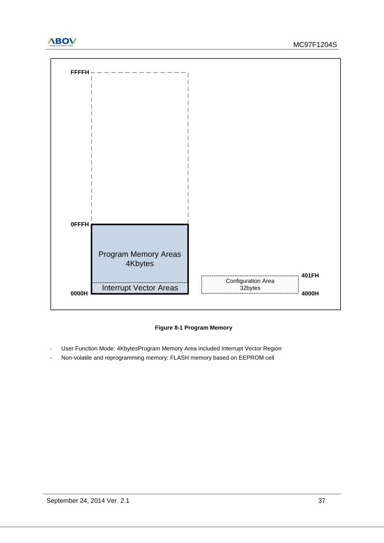
A 16-bit program counter is capable of addressing up to 64Kbytes for one bank of memory space,
but this device has 4Kbytes program memory space.
Figure 8-1 shows a map of program memory. After reset, the CPU begins execution from location
0000H. Each interrupt is assigned a fixed location in program memory. The interrupt causes the CPU
to jump to that location, where it commences execution of the service routine.
External interrupt 0, for example, is assigned to location 0003H. If external interrupt 0 is going to be used, its service routine must begin at location 0003H. If the interrupt is not going to be used, its service location is available as general purpose program memory. If an interrupt service routine is short enough (as is often the case in control applications),it can reside entirely within that 8 byte interval. Longer service routines can use a jump instruction to skip over subsequent interrupt locations, if other interrupts are in use.
MC97F1204S
September 24, 2014 Ver. 2.1 37
Program Memory Areas
4Kbytes
0000H
0FFFH
FFFFH
Interrupt Vector Areas
401FHConfiguration Area
32bytes4000H
Figure 8-1 Program Memory
- User Function Mode: 4KbytesProgram Memory Area included Interrupt Vector Region
- Non-volatile and reprogramming memory: FLASH memory based on EEPROM cell
MC97F1204S
38 September 24, 2014 Ver. 2.1
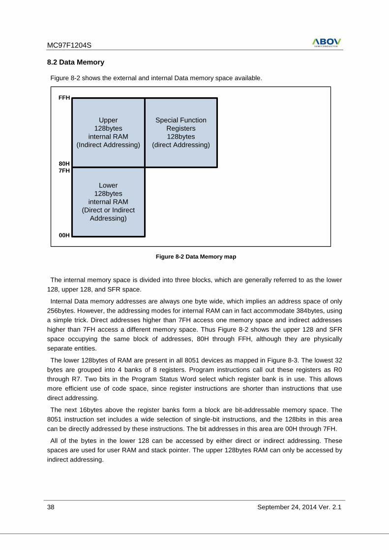
8.2 Data Memory
Figure 8-2 shows the external and internal Data memory space available.
Upper
128bytes
internal RAM
(Indirect Addressing)
FFH
80H
Lower
128bytes
internal RAM
(Direct or Indirect
Addressing)
Special Function
Registers
128bytes
(direct Addressing)
00H
7FH
Figure 8-2 Data Memory map
The internal memory space is divided into three blocks, which are generally referred to as the lower
128, upper 128, and SFR space.
Internal Data memory addresses are always one byte wide, which implies an address space of only
256bytes. However, the addressing modes for internal RAM can in fact accommodate 384bytes, using
a simple trick. Direct addresses higher than 7FH access one memory space and indirect addresses
higher than 7FH access a different memory space. Thus Figure 8-2 shows the upper 128 and SFR
space occupying the same block of addresses, 80H through FFH, although they are physically
separate entities.
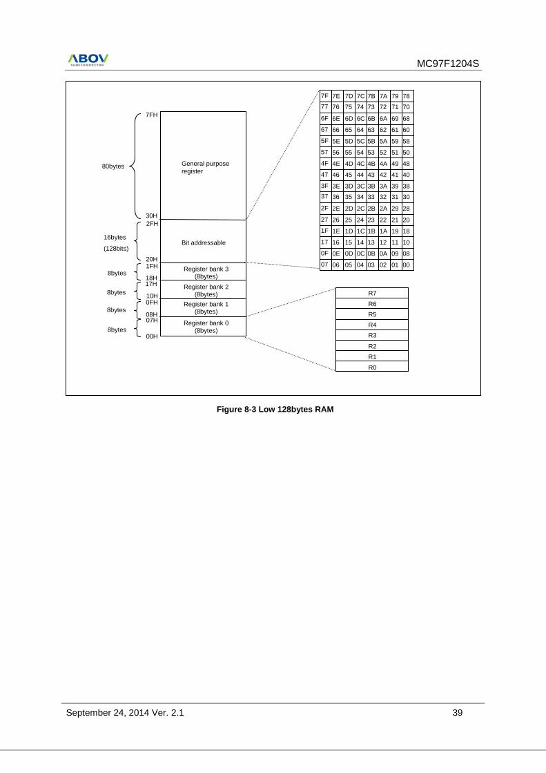
The lower 128bytes of RAM are present in all 8051 devices as mapped in Figure 8-3. The lowest 32
bytes are grouped into 4 banks of 8 registers. Program instructions call out these registers as R0
through R7. Two bits in the Program Status Word select which register bank is in use. This allows
more efficient use of code space, since register instructions are shorter than instructions that use
direct addressing.
The next 16bytes above the register banks form a block are bit-addressable memory space. The
8051 instruction set includes a wide selection of single-bit instructions, and the 128bits in this area
can be directly addressed by these instructions. The bit addresses in this area are 00H through 7FH.
All of the bytes in the lower 128 can be accessed by either direct or indirect addressing. These
spaces are used for user RAM and stack pointer. The upper 128bytes RAM can only be accessed by
indirect addressing.
MC97F1204S
September 24, 2014 Ver. 2.1 39
00 01 02 03 04 05 06 07
08 09 0A 0B 0C 0D 0E 0F
10 11 12 13 14 15 16 17
18 19 1A 1B 1C 1D 1E 1F
20 21 22 23 24 25 26 27
28 29 2A 2B 2C 2D 2E 2F
30 31 32 33 34 35 36 37
38 39 3A 3B 3C 3D 3E 3F
40 41 42 43 44 45 46 47
48 49 4A 4B 4C 4D 4E 4F
50 51 52 53 54 55 56 57
58 59 5A 5B 5C 5D 5E 5F
60 61 62 63 64 65 66 67
68 69 6A 6B 6C 6D 6E 6F
70 71 72 73 74 75 76 77
78 79 7A 7B 7C 7D 7E 7F
R5
R4
R3
R2
R1
R0
R6
R7
2FH
Register bank 0 (8bytes)
Register bank 1 (8bytes)
Register bank 2 (8bytes)
Register bank 3 (8bytes)
Bit addressable
General purpose
register
20H
18H 17H
10H 0FH
08H 07H
00H
30H
7FH
1FH
80bytes
16bytes
(128bits)
8bytes
8bytes
8bytes
8bytes
Figure 8-3 Low 128bytes RAM
MC97F1204S
40 September 24, 2014 Ver. 2.1
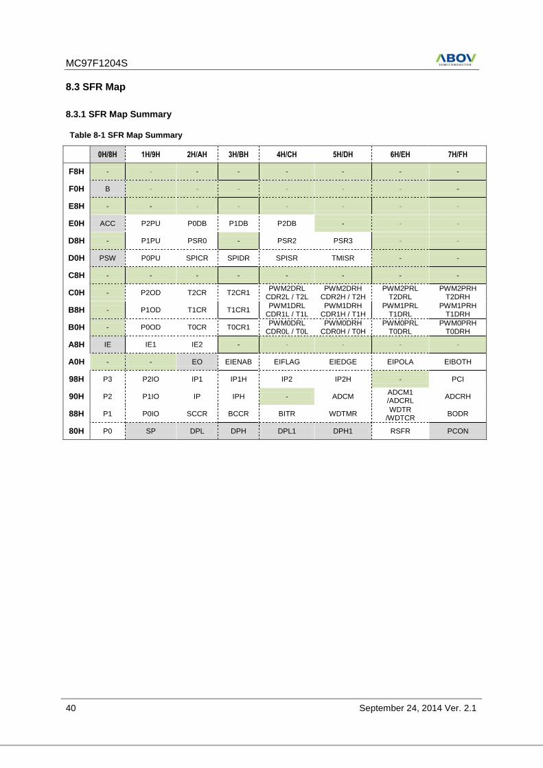
8.3 SFR Map
8.3.1 SFR Map Summary
Table 8-1 SFR Map Summary
0H/8H 1H/9H 2H/AH 3H/BH 4H/CH 5H/DH 6H/EH 7H/FH
F8H - - - - - - - -
F0H B - - - - - - -
E8H - - - - - - - -
E0H ACC P2PU P0DB P1DB P2DB - - -
D8H - P1PU PSR0 - PSR2 PSR3 - -
D0H PSW P0PU SPICR SPIDR SPISR TMISR - -
C8H - - - - - - - -
C0H - P2OD T2CR T2CR1 PWM2DRL
CDR2L / T2L PWM2DRH
CDR2H / T2H PWM2PRL
T2DRL PWM2PRH
T2DRH
B8H - P1OD T1CR T1CR1 PWM1DRL
CDR1L / T1L PWM1DRH
CDR1H / T1H PWM1PRL
T1DRL PWM1PRH
T1DRH
B0H - P0OD T0CR T0CR1 PWM0DRL
CDR0L / T0L PWM0DRH
CDR0H / T0H PWM0PRL
T0DRL PWM0PRH
T0DRH
A8H IE IE1 IE2 - - - - -
A0H - - EO EIENAB EIFLAG EIEDGE EIPOLA EIBOTH
98H P3 P2IO IP1 IP1H IP2 IP2H - PCI
90H P2 P1IO IP IPH - ADCM ADCM1 /ADCRL
ADCRH
88H P1 P0IO SCCR BCCR BITR WDTMR WDTR
/WDTCR BODR
80H P0 SP DPL DPH DPL1 DPH1 RSFR PCON
MC97F1204S
September 24, 2014 Ver. 2.1 41
8.3.2 Compiler Compatible SFR
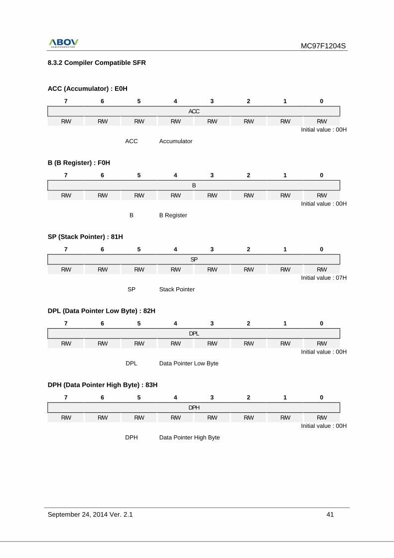
ACC (Accumulator) : E0H
7 6 5 4 3 2 1 0
ACC
R/W R/W R/W R/W R/W R/W R/W R/W
Initial value : 00H
ACC Accumulator
B (B Register) : F0H
7 6 5 4 3 2 1 0
B
R/W R/W R/W R/W R/W R/W R/W R/W
Initial value : 00H
B B Register
SP (Stack Pointer) : 81H
7 6 5 4 3 2 1 0
SP
R/W R/W R/W R/W R/W R/W R/W R/W
Initial value : 07H
SP Stack Pointer
DPL (Data Pointer Low Byte) : 82H
7 6 5 4 3 2 1 0
DPL
R/W R/W R/W R/W R/W R/W R/W R/W
Initial value : 00H
DPL Data Pointer Low Byte
DPH (Data Pointer High Byte) : 83H
7 6 5 4 3 2 1 0
DPH
R/W R/W R/W R/W R/W R/W R/W R/W
Initial value : 00H
DPH Data Pointer High Byte
MC97F1204S
42 September 24, 2014 Ver. 2.1
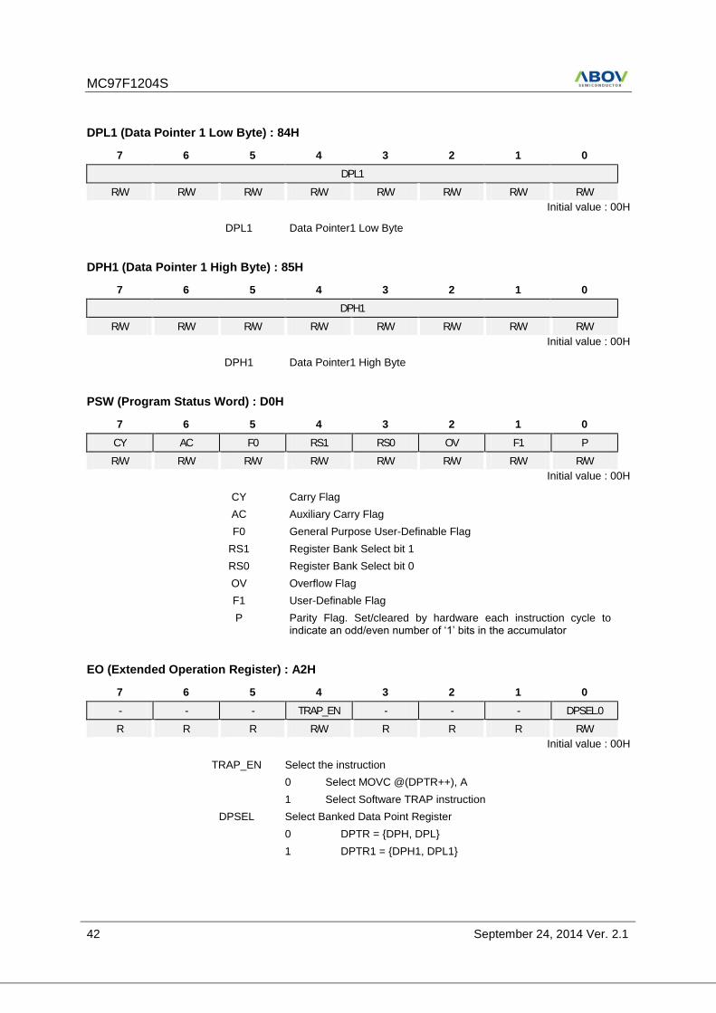
DPL1 (Data Pointer 1 Low Byte) : 84H
7 6 5 4 3 2 1 0
DPL1
R/W R/W R/W R/W R/W R/W R/W R/W
Initial value : 00H
DPL1 Data Pointer1 Low Byte
DPH1 (Data Pointer 1 High Byte) : 85H
7 6 5 4 3 2 1 0
DPH1
R/W R/W R/W R/W R/W R/W R/W R/W
Initial value : 00H
DPH1 Data Pointer1 High Byte
PSW (Program Status Word) : D0H
7 6 5 4 3 2 1 0
CY AC F0 RS1 RS0 OV F1 P
R/W R/W R/W R/W R/W R/W R/W R/W
Initial value : 00H
CY Carry Flag
AC Auxiliary Carry Flag
F0 General Purpose User-Definable Flag
RS1 Register Bank Select bit 1
RS0 Register Bank Select bit 0
OV Overflow Flag
F1 User-Definable Flag
P Parity Flag. Set/cleared by hardware each instruction cycle to indicate an odd/even number of ‘1’ bits in the accumulator
EO (Extended Operation Register) : A2H
7 6 5 4 3 2 1 0
- - - TRAP_EN - - - DPSEL.0
R R R R/W R R R R/W
Initial value : 00H
TRAP_EN Select the instruction
0 Select MOVC @(DPTR++), A
1 Select Software TRAP instruction
DPSEL Select Banked Data Point Register
0 DPTR = {DPH, DPL}
1 DPTR1 = {DPH1, DPL1}
MC97F1204S
September 24, 2014 Ver. 2.1 43
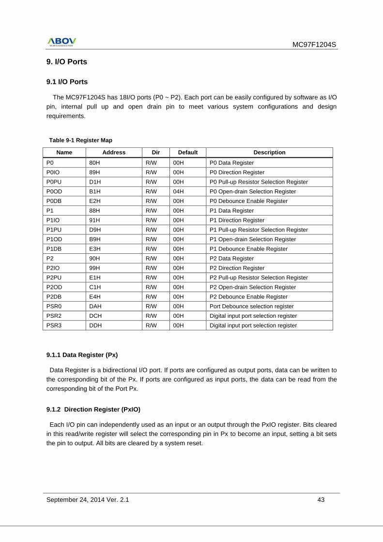
9. I/O Ports
9.1 I/O Ports
The MC97F1204S has 18I/O ports (P0 ~ P2). Each port can be easily configured by software as I/O
pin, internal pull up and open drain pin to meet various system configurations and design
requirements.
Table 9-1 Register Map
Name Address Dir Default Description
P0 80H R/W 00H P0 Data Register
P0IO 89H R/W 00H P0 Direction Register
P0PU D1H R/W 00H P0 Pull-up Resistor Selection Register
P0OD B1H R/W 04H P0 Open-drain Selection Register
P0DB E2H R/W 00H P0 Debounce Enable Register
P1 88H R/W 00H P1 Data Register
P1IO 91H R/W 00H P1 Direction Register
P1PU D9H R/W 00H P1 Pull-up Resistor Selection Register
P1OD B9H R/W 00H P1 Open-drain Selection Register
P1DB E3H R/W 00H P1 Debounce Enable Register
P2 90H R/W 00H P2 Data Register
P2IO 99H R/W 00H P2 Direction Register
P2PU E1H R/W 00H P2 Pull-up Resistor Selection Register
P2OD C1H R/W 00H P2 Open-drain Selection Register
P2DB E4H R/W 00H P2 Debounce Enable Register
PSR0 DAH R/W 00H Port Debounce selection register
PSR2 DCH R/W 00H Digital input port selection register
PSR3 DDH R/W 00H Digital input port selection register
9.1.1 Data Register (Px)
Data Register is a bidirectional I/O port. If ports are configured as output ports, data can be written to
the corresponding bit of the Px. If ports are configured as input ports, the data can be read from the
corresponding bit of the Port Px.
9.1.2 Direction Register (PxIO)
Each I/O pin can independently used as an input or an output through the PxIO register. Bits cleared
in this read/write register will select the corresponding pin in Px to become an input, setting a bit sets
the pin to output. All bits are cleared by a system reset.
MC97F1204S
44 September 24, 2014 Ver. 2.1
9.1.3 Pull-up Resistor Selection Register (PxPU)
The on-chip pull-up resistor can be connected to them in 1-bit units with a pull-up resistor selection
register (PxPU). The pull-up register selection controls the pull-up resister enable/disable of each port.
When the corresponding bit is 1, the pull-up resister of the pin is enabled. When 0, the pull-up resister
is disabled. All bits are cleared by a system reset.
9.1.4 Open-drain Selection Register (PxOD)
The open-drain selection register controls the open-drain enable/disable of each port. Ports become
push-pull by a system reset. You should connect an internal resistor or an external resistor in open-
drain output mode.
9.1.5 De-bounce Enable Register (PxDB)
P0 ~ P3 support de-bounce function. De-bounce time of each port has 1/2/4/8us
9.1.6 Port Selection Register (PSR0, PSR2, PSR3)
PSR0 :Port debounce selection register can select one of four debounce length of all port.
PSR2, PSR3 : Digital Input port selection register can select use of port's Digital input or not.
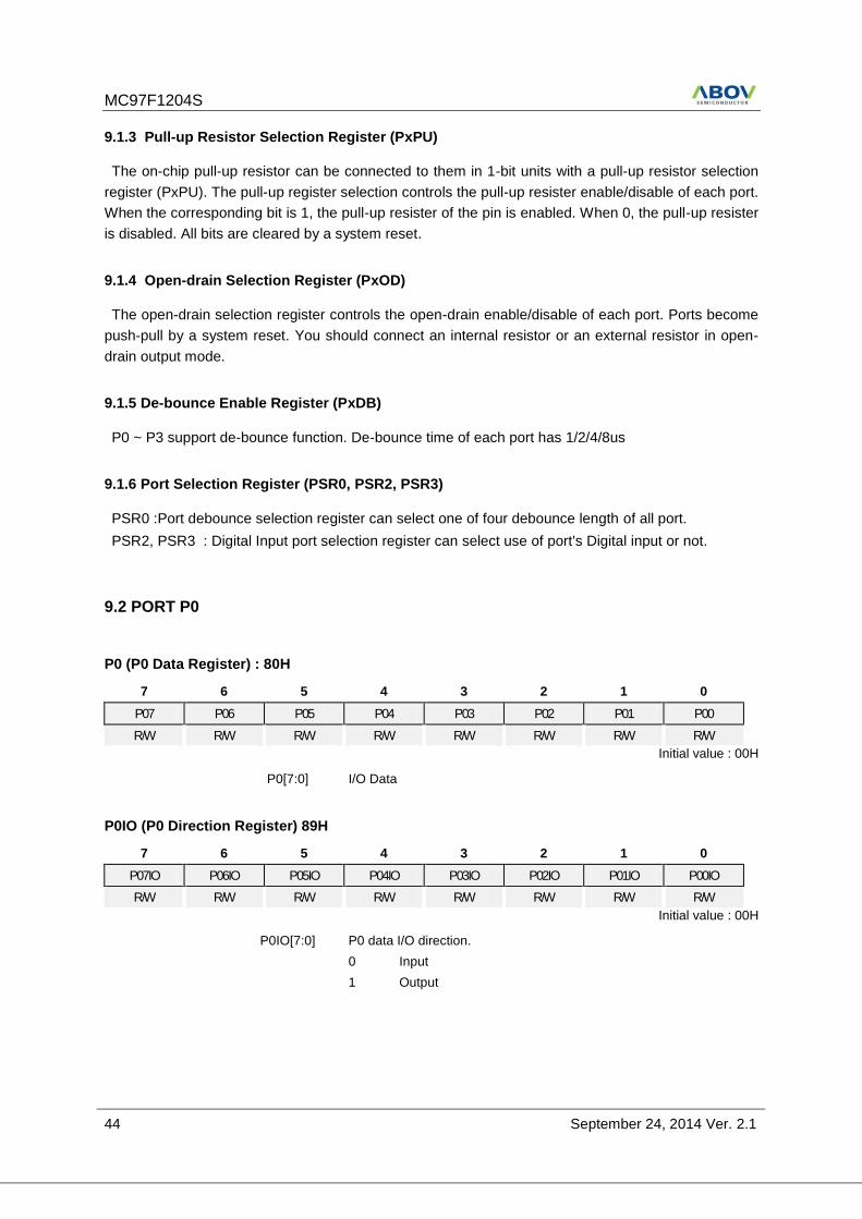
9.2 PORT P0
P0 (P0 Data Register) : 80H
7 6 5 4 3 2 1 0
P07 P06 P05 P04 P03 P02 P01 P00
R/W R/W R/W R/W R/W R/W R/W R/W
Initial value : 00H
P0[7:0] I/O Data
P0IO (P0 Direction Register) 89H
7 6 5 4 3 2 1 0
P07IO P06IO P05IO P04IO P03IO P02IO P01IO P00IO
R/W R/W R/W R/W R/W R/W R/W R/W
Initial value : 00H
P0IO[7:0] P0 data I/O direction.
0 Input
1 Output
MC97F1204S
September 24, 2014 Ver. 2.1 45
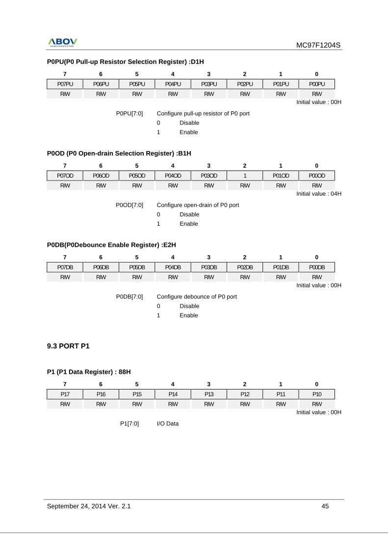
P0PU(P0 Pull-up Resistor Selection Register) :D1H
7 6 5 4 3 2 1 0
P07PU P06PU P05PU P04PU P03PU P02PU P01PU P00PU
R/W R/W R/W R/W R/W R/W R/W R/W
Initial value : 00H
P0PU[7:0] Configure pull-up resistor of P0 port
0 Disable
1 Enable
P0OD (P0 Open-drain Selection Register) :B1H
7 6 5 4 3 2 1 0
P07OD P06OD P05OD P04OD P03OD 1 P01OD P00OD
R/W R/W R/W R/W R/W R/W R/W R/W
Initial value : 04H
P0OD[7:0] Configure open-drain of P0 port
0 Disable
1 Enable
P0DB(P0Debounce Enable Register) :E2H
7 6 5 4 3 2 1 0
P07DB P06DB P05DB P04DB P03DB P02DB P01DB P00DB
R/W R/W R/W R/W R/W R/W R/W R/W
Initial value : 00H
P0DB[7:0] Configure debounce of P0 port
0 Disable
1 Enable
9.3 PORT P1
P1 (P1 Data Register) : 88H
7 6 5 4 3 2 1 0
P17 P16 P15 P14 P13 P12 P11 P10
R/W R/W R/W R/W R/W R/W R/W R/W
Initial value : 00H
P1[7:0] I/O Data
MC97F1204S
46 September 24, 2014 Ver. 2.1
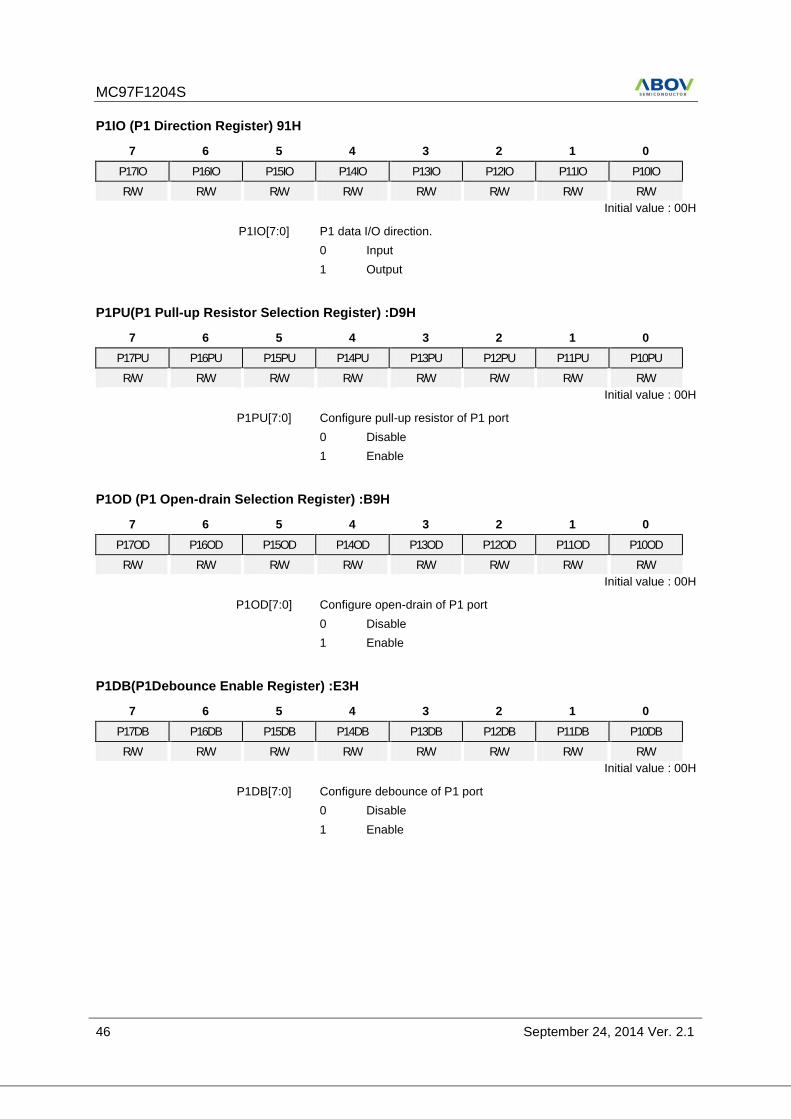
P1IO (P1 Direction Register) 91H
7 6 5 4 3 2 1 0
P17IO P16IO P15IO P14IO P13IO P12IO P11IO P10IO
R/W R/W R/W R/W R/W R/W R/W R/W
Initial value : 00H
P1IO[7:0] P1 data I/O direction.
0 Input
1 Output
P1PU(P1 Pull-up Resistor Selection Register) :D9H
7 6 5 4 3 2 1 0
P17PU P16PU P15PU P14PU P13PU P12PU P11PU P10PU
R/W R/W R/W R/W R/W R/W R/W R/W
Initial value : 00H
P1PU[7:0] Configure pull-up resistor of P1 port
0 Disable
1 Enable
P1OD (P1 Open-drain Selection Register) :B9H
7 6 5 4 3 2 1 0
P17OD P16OD P15OD P14OD P13OD P12OD P11OD P10OD
R/W R/W R/W R/W R/W R/W R/W R/W
Initial value : 00H
P1OD[7:0] Configure open-drain of P1 port
0 Disable
1 Enable
P1DB(P1Debounce Enable Register) :E3H
7 6 5 4 3 2 1 0
P17DB P16DB P15DB P14DB P13DB P12DB P11DB P10DB
R/W R/W R/W R/W R/W R/W R/W R/W
Initial value : 00H
P1DB[7:0] Configure debounce of P1 port
0 Disable
1 Enable
MC97F1204S
September 24, 2014 Ver. 2.1 47
9.4 PORT P2
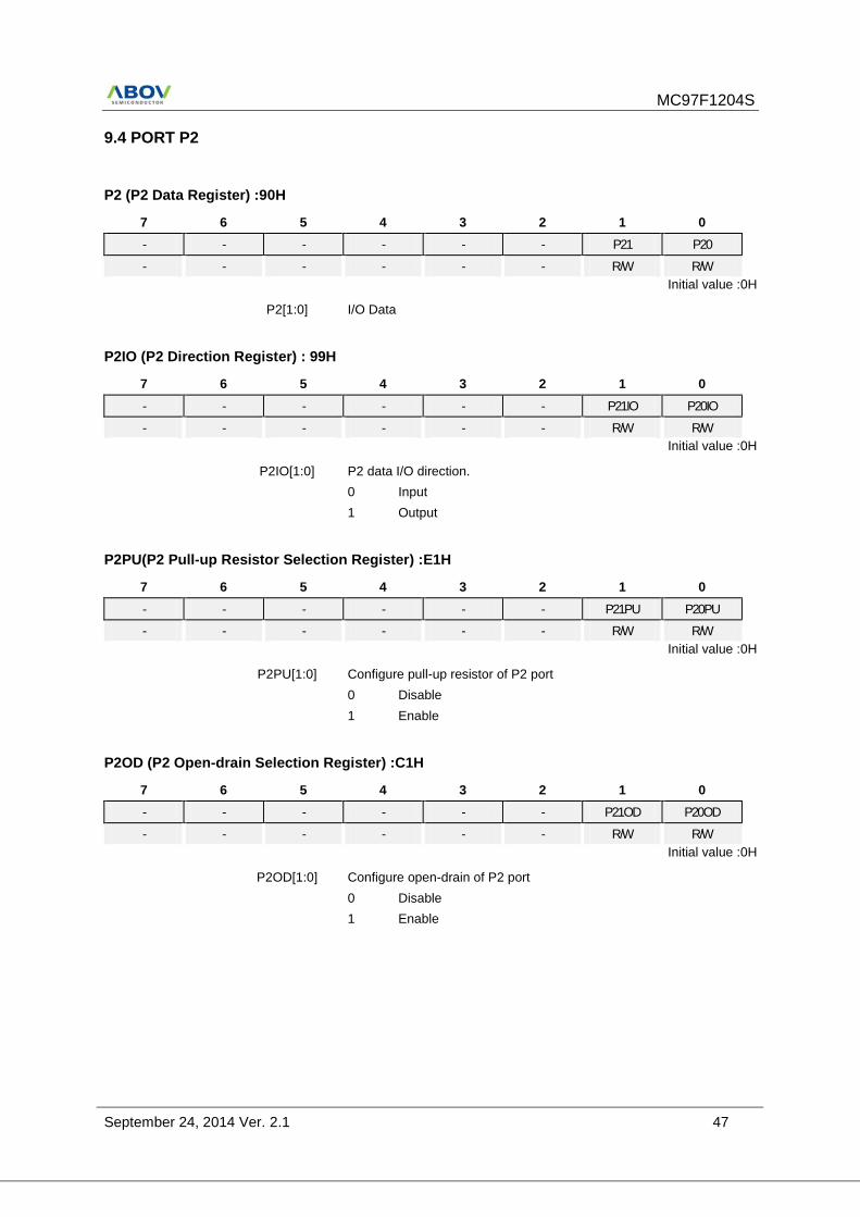
P2 (P2 Data Register) :90H
7 6 5 4 3 2 1 0
- - - - - - P21 P20
- - - - - - R/W R/W
Initial value :0H
P2[1:0] I/O Data
P2IO (P2 Direction Register) : 99H
7 6 5 4 3 2 1 0
- - - - - - P21IO P20IO
- - - - - - R/W R/W
Initial value :0H
P2IO[1:0] P2 data I/O direction.
0 Input
1 Output
P2PU(P2 Pull-up Resistor Selection Register) :E1H
7 6 5 4 3 2 1 0
- - - - - - P21PU P20PU
- - - - - - R/W R/W
Initial value :0H
P2PU[1:0] Configure pull-up resistor of P2 port
0 Disable
1 Enable
P2OD (P2 Open-drain Selection Register) :C1H
7 6 5 4 3 2 1 0
- - - - - - P21OD P20OD
- - - - - - R/W R/W
Initial value :0H
P2OD[1:0] Configure open-drain of P2 port
0 Disable
1 Enable
MC97F1204S
48 September 24, 2014 Ver. 2.1
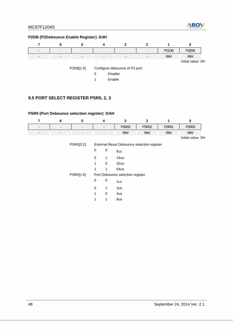
P2DB (P2Debounce Enable Register) :E4H
7 6 5 4 3 2 1 0
- - - - - - P21DB P20DB
- - - - - - R/W R/W
Initial value :0H
P2DB[1:0] Configure debounce of P2 port
0 Disable
1 Enable
9.5 PORT SELECT REGISTER PSR0, 2, 3
PSR0 (Port Debounce selection register) :DAH
7 6 5 4 3 2 1 0
- - - - PSR03 PSR02 PSR01 PSR00
- - - - R/W R/W R/W R/W
Initial value :0H
PSR0[3:2] External Reset Debounce selection register
0 0 8us
0 1 16us
1 0 32us
1 1 64us
PSR0[1:0] Port Debounce selection register
0 0 1us
0 1 2us
1 0 4us
1 1 8us
MC97F1204S
September 24, 2014 Ver. 2.1 49
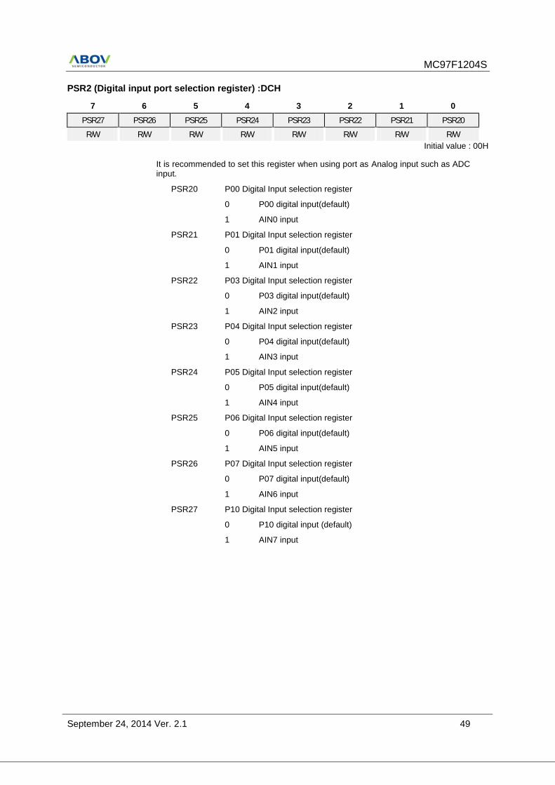
PSR2 (Digital input port selection register) :DCH
7 6 5 4 3 2 1 0
PSR27 PSR26 PSR25 PSR24 PSR23 PSR22 PSR21 PSR20
R/W R/W R/W R/W R/W R/W R/W R/W
Initial value : 00H
It is recommended to set this register when using port as Analog input such as ADC input.
PSR20 P00 Digital Input selection register
0 P00 digital input(default)
1 AIN0 input
PSR21 P01 Digital Input selection register
0 P01 digital input(default)
1 AIN1 input
PSR22 P03 Digital Input selection register
0 P03 digital input(default)
1 AIN2 input
PSR23 P04 Digital Input selection register
0 P04 digital input(default)
1 AIN3 input
PSR24 P05 Digital Input selection register
0 P05 digital input(default)
1 AIN4 input
PSR25 P06 Digital Input selection register
0 P06 digital input(default)
1 AIN5 input
PSR26 P07 Digital Input selection register
0 P07 digital input(default)
1 AIN6 input
PSR27 P10 Digital Input selection register
0 P10 digital input (default)
1 AIN7 input
MC97F1204S
50 September 24, 2014 Ver. 2.1
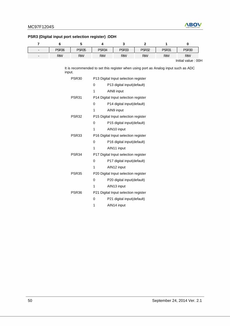
PSR3 (Digital input port selection register) :DDH
7 6 5 4 3 2 1 0
- PSR36 PSR35 PSR34 PSR33 PSR32 PSR31 PSR30
- R/W R/W R/W R/W R/W R/W R/W
Initial value : 00H
It is recommended to set this register when using port as Analog input such as ADC input.
PSR30 P13 Digital Input selection register
0 P13 digital input(default)
1 AIN8 input
PSR31 P14 Digital Input selection register
0 P14 digital input(default)
1 AIN9 input
PSR32 P15 Digital Input selection register
0 P15 digital input(default)
1 AIN10 input
PSR33 P16 Digital Input selection register
0 P16 digital input(default)
1 AIN11 input
PSR34 P17 Digital Input selection register
0 P17 digital input(default)
1 AIN12 input
PSR35 P20 Digital Input selection register
0 P20 digital input(default)
1 AIN13 input
PSR36 P21 Digital Input selection register
0 P21 digital input(default)
1 AIN14 input
MC97F1204S
September 24, 2014 Ver. 2.1 51
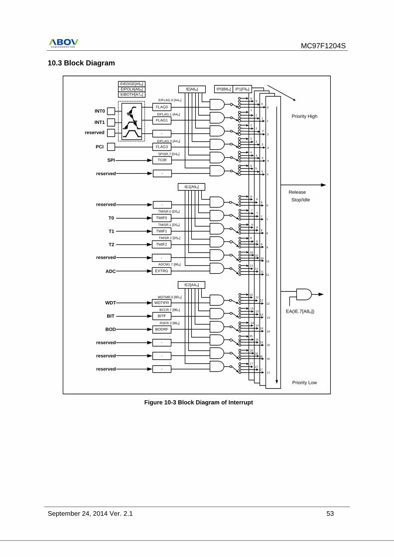
10. Interrupt Controller
10.1 Overview
The MC97F1204S supports up to 12 interrupt sources. The interrupts have separate enable register
bits associated with them, allowing software control. They can also have four levels of priority
assigned to them. The interrupt controller has following features:
- receive the request from 11 interrupt source
- 4 priority levels
- Multi Interrupt possibility
- If the requests of different priority are received simultaneously, the request of higher priority is serviced first and then lower priority is serviced.
- Each interrupt source can be controlled by EA bit and each IEx bit
- Interrupt latency: 5~8 machine cycles in single interrupt system
The maskable interrupts are enabled through three pair of interrupt enable registers (IE, IE1,
IE2).Bits of IE, IE1, IE2register each individually enable/disable a particular interrupt source. Overall
control is provided by EA (bit 7 of IE). When EA is set to ‘0’, all interrupts are disabled: when EA is set
to ‘1’, interrupts are individually enabled or disabled through the other bits of the interrupt enable
registers. The MC97F1204S supports a 4-level priority scheme. Each maskable interrupt is
individually assigned to one of four priority levels by writing to IPx or IPHx.
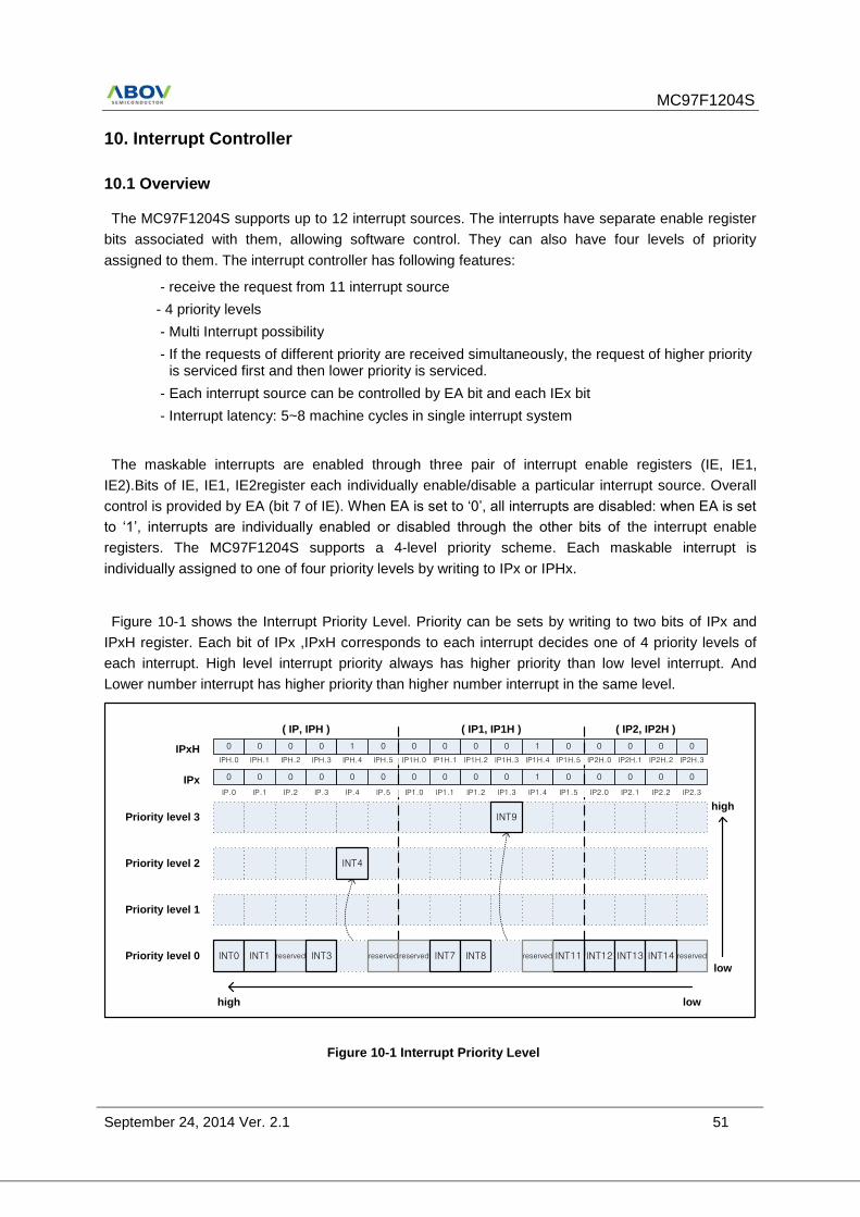
Figure 10-1 shows the Interrupt Priority Level. Priority can be sets by writing to two bits of IPx and
IPxH register. Each bit of IPx ,IPxH corresponds to each interrupt decides one of 4 priority levels of
each interrupt. High level interrupt priority always has higher priority than low level interrupt. And
Lower number interrupt has higher priority than higher number interrupt in the same level.
Priority level 0 INT0 reserved INT12 INT13
Priority level 1
Priority level 2
Priority level 3
0 0 0 0 0 0 0 0 0 0 1 0 0 0 0 0
0 0 0 0 1 0 0 0 0 0 1 0 0 0 0 0IPxH
IPx
( IP, IPH ) ( IP1, IP1H ) ( IP2, IP2H )
high low
high
low
INT4
IPH.0 IPH.1 IPH.2 IPH.3 IPH.4 IPH.5 IP1H.0 IP1H.1 IP1H.2 IP1H.3 IP1H.4 IP1H.5 IP2H.0 IP2H.1 IP2H.2 IP2H.3
IP.0 IP.1 IP.2 IP.3 IP.4 IP.5 IP1.0 IP1.1 IP1.2 IP1.3 IP1.4 IP1.5 IP2.0 IP2.1 IP2.2 IP2.3
reserved reserved reserved
INT9
INT11 INT14INT7INT3INT1 INT8 reserved
Figure 10-1 Interrupt Priority Level
MC97F1204S
52 September 24, 2014 Ver. 2.1
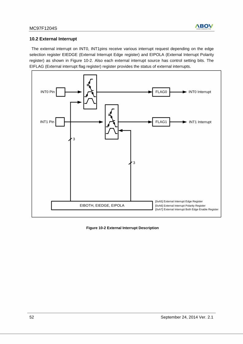
10.2 External Interrupt
The external interrupt on INT0, INT1pins receive various interrupt request depending on the edge
selection register EIEDGE (External Interrupt Edge register) and EIPOLA (External Interrupt Polarity
register) as shown in Figure 10-2. Also each external interrupt source has control setting bits. The
EIFLAG (External interrupt flag register) register provides the status of external interrupts.
EIBOTH, EIEDGE, EIPOLA
INT0 Pin
INT1 Pin
FLAG0
FLAG1
INT0 Interrupt
INT1 Interrupt
[0xA5] External Interrupt Edge Register
[0xA6] External Interrupt Polarity Register
[0xA7] External Interrupt Both Edge Enable Register
3
3
Figure 10-2 External Interrupt Description
MC97F1204S
September 24, 2014 Ver. 2.1 53
10.3 Block Diagram
Release
Stop/Idle
EA(IE.7[A8H])
Priority High
Priority Low
FLAG0
FLAG1
-
FLAG3
IE[A8H]
EIFLAG.0 [A4H]
EIFLAG.1 [A4H]
EIFLAG.3 [A4H]
INT0
INT1
0
1
2
3
4
5
0
1
2
3
4
5
0
1
2
3
4
5
0
1
2
3
4
5
EIEDGE[A5H]
IP0[B8H] IP1[F8H]EIPOLA[A6H]
EIBOTH[A7H]
SPI
IE2[AAH]
12
13
14
15
16
17
12
13
14
15
16
17
12
13
14
15
16
17
12
13
14
15
16
17
PCI
TCIR
SPISR.7 [D4H]
-
IE1[A9H]
6
7
8
9
10
11
6
7
8
9
10
11
6
7
8
9
10
11
-
TMIF0
TMIF1
TMIF2
-
T0
T1
T2
TMISR.0 [D5H]
TMISR.1 [D5H]
TMISR.2 [D5H]
EXTRGADC
ADCM1.7 [96H]
WDTIFR
WDTMR.0 [8DH]
WDT
BITFBIT
BCCR.7 [8BH]
BODRFBOD
RSFR.3 [86H]
-reserved
-
-reserved
-
-reserved
-
reserved
reserved
reserved
reserved
6
7
8
9
10
11
Figure 10-3 Block Diagram of Interrupt
MC97F1204S
54 September 24, 2014 Ver. 2.1
10.4 Interrupt Vector Table
The interrupt controller supports 12 interrupt sources as shown in the Table 10-1 below. When
interrupt becomes service, long call instruction (LCALL) is executed in the vector address. Interrupt
request 12 has a decided priority order.
Table 10-1 Interrupt Vector Address Table
Interrupt Source Symbol Interrupt
Enable Bit Priority Mask Vector Address
Hardware Reset RESETB 0 0 Non-Maskable 0000H
External Interrupt 0 INT0 IE.0 1 Maskable 0003H
External Interrupt 1 INT1 IE.1 2 Maskable 000BH
Reserved INT2 IE.2 3 Maskable 0013H
PCI INT3 IE.3 4 Maskable 001BH
SPI INT4 IE.4 5 Maskable 0023H
Reserved INT5 IE.5 6 Maskable 002BH
Reserved INT6 IE1.0 7 Maskable 0033H
T0 INT7 IE1.1 8 Maskable 003BH
T1 INT8 IE1.2 9 Maskable 0043H
T2 INT9 IE1.3 10 Maskable 004BH
Reserved INT10 IE1.4 11 Maskable 0053H
ADC INT11 IE1.5 12 Maskable 005BH
WDT INT12 IE2.0 13 Maskable 0063H
BIT INT13 IE2.1 14 Maskable 006BH
BOD INT14 IE2.2 15 Maskable 0073H
Reserved INT15 IE2.3 16 Maskable 007BH
Reserved INT16 IE2.4 17 Maskable 0083H
Reserved INT17 IE2.5 18 Maskable 008BH
For mask-able interrupt execution, first EA bit must set ‘1’ and specific interrupt source must set ‘1’
by writing a ‘1’ to associated bit in the IEx. If interrupt request is received, specific interrupt request
flag set ‘1’. And it remains ‘1’ until CPU accepts interrupt. After that, interrupt request flag will be
cleared automatically.
MC97F1204S
September 24, 2014 Ver. 2.1 55
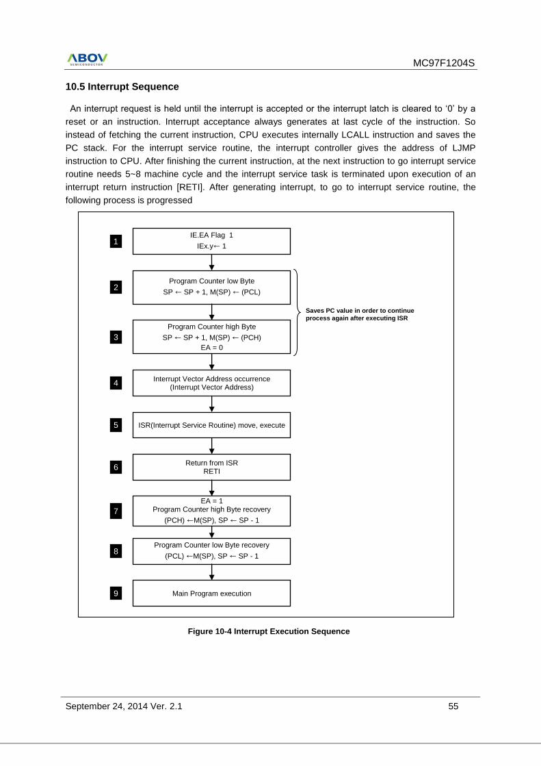
10.5 Interrupt Sequence
An interrupt request is held until the interrupt is accepted or the interrupt latch is cleared to ‘0’ by a
reset or an instruction. Interrupt acceptance always generates at last cycle of the instruction. So
instead of fetching the current instruction, CPU executes internally LCALL instruction and saves the
PC stack. For the interrupt service routine, the interrupt controller gives the address of LJMP
instruction to CPU. After finishing the current instruction, at the next instruction to go interrupt service
routine needs 5~8 machine cycle and the interrupt service task is terminated upon execution of an
interrupt return instruction [RETI]. After generating interrupt, to go to interrupt service routine, the
following process is progressed
Saves PC value in order to continue
process again after executing ISR
IE.EA Flag 1
IEx.y← 1 1
Program Counter low Byte
SP ← SP + 1, M(SP) ← (PCL) 2
Program Counter high Byte
SP ← SP + 1, M(SP) ← (PCH)
EA = 0
3
Interrupt Vector Address occurrence (Interrupt Vector Address)
4
ISR(Interrupt Service Routine) move, execute 5
Return from ISR RETI
6
EA = 1 Program Counter high Byte recovery
(PCH) ←M(SP), SP ← SP - 1
7
Main Program execution 9
Program Counter low Byte recovery
(PCL) ←M(SP), SP ← SP - 1 8
Figure 10-4 Interrupt Execution Sequence
MC97F1204S
56 September 24, 2014 Ver. 2.1
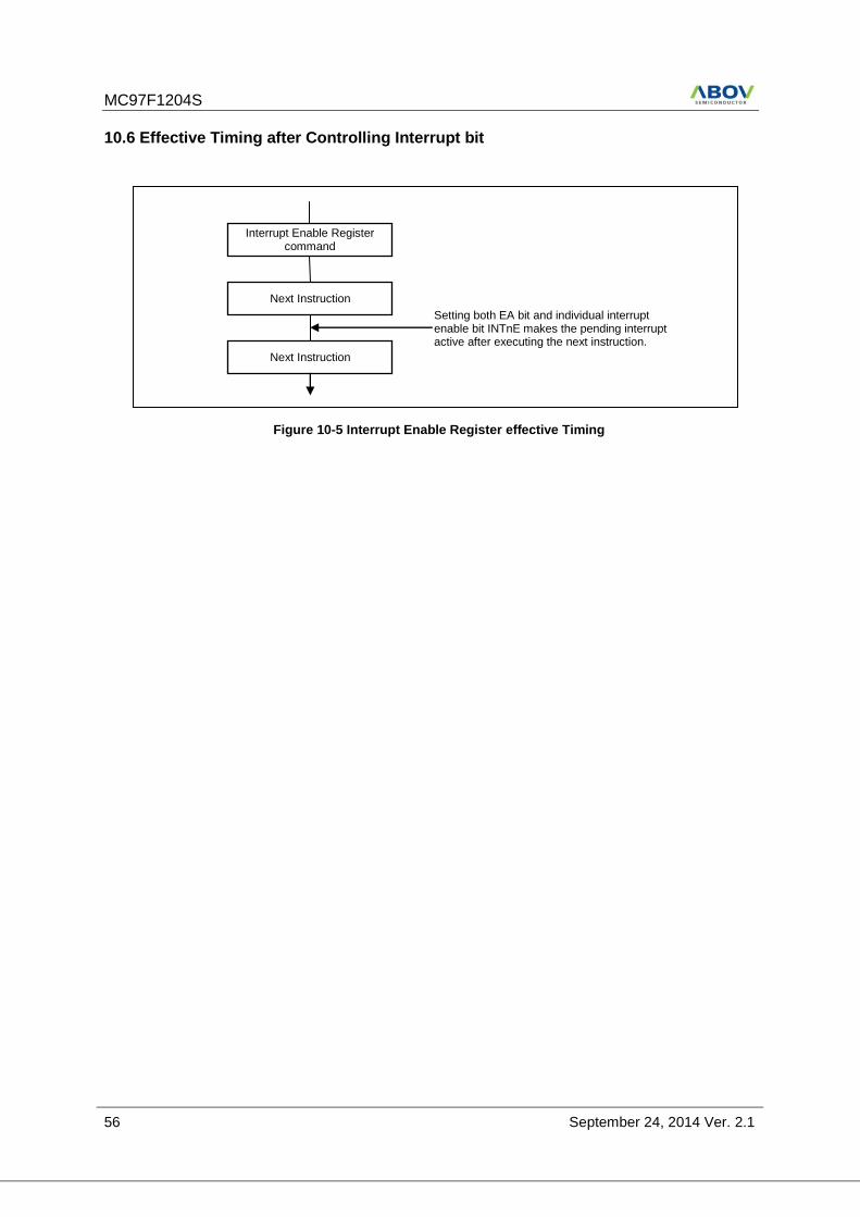
10.6 Effective Timing after Controlling Interrupt bit
Interrupt Enable Register command
Next Instruction
Next Instruction
Setting both EA bit and individual interrupt enable bit INTnE makes the pending interrupt active after executing the next instruction.
Figure 10-5 Interrupt Enable Register effective Timing
MC97F1204S
September 24, 2014 Ver. 2.1 57
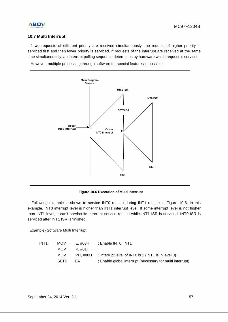
10.7 Multi Interrupt
If two requests of different priority are received simultaneously, the request of higher priority is
serviced first and then lower priority is serviced. If requests of the interrupt are received at the same
time simultaneously, an interrupt polling sequence determines by hardware which request is serviced.
However, multiple processing through software for special features is possible.
Following example is shown to service INT0 routine during INT1 routine in Figure 10-6. In this
example, INT0 interrupt level is higher than INT1 interrupt level. If some interrupt level is not higher
than INT1 level, it can’t service its interrupt service routine while INT1 ISR is serviced. INT0 ISR is
serviced after INT1 ISR is finished.
Example) Software Multi Interrupt:
INT1: MOV IE, #03H ; Enable INT0, INT1
MOV IP, #01H
MOV IPH, #00H ; interrupt level of INT0 is 1 (INT1 is in level 0)
SETB EA ; Enable global interrupt (necessary for multi interrupt)
:
Figure 10-6 Execution of Multi Interrupt
Main Program
Service
Occur
INT1 Interrupt
INT1 ISR
SETB EA
Occur
INT0 Interrupt
INT0 ISR
RETI
RETI
MC97F1204S
58 September 24, 2014 Ver. 2.1
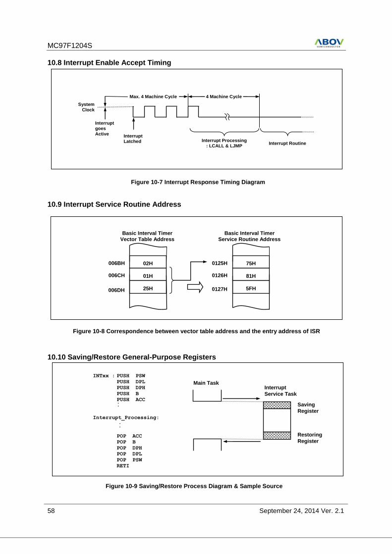
10.8 Interrupt Enable Accept Timing
10.9 Interrupt Service Routine Address
10.10 Saving/Restore General-Purpose Registers
02H
01H
006BH
006CH
Basic Interval Timer Vector Table Address
75H
81H
0125H
0126H
Basic Interval Timer Service Routine Address
25H 5FH 006DH 0127H 0127H
Interrupt Latched
Interrupt goes
Active
System
Clock
Max. 4 Machine Cycle 4 Machine Cycle
Interrupt Processing : LCALL & LJMP
Interrupt Routine
Figure 10-7 Interrupt Response Timing Diagram
Figure 10-8 Correspondence between vector table address and the entry address of ISR
Main Task
Saving
Register
Restoring
Register
Interrupt
Service Task
INTxx : PUSH PSW
PUSH DPL
PUSH DPH
PUSH B
PUSH ACC ∙ ∙
Interrupt_Processing:
∙ ∙
POP ACC
POP B
POP DPH
POP DPL
POP PSW
RETI
Figure 10-9 Saving/Restore Process Diagram & Sample Source
MC97F1204S
September 24, 2014 Ver. 2.1 59
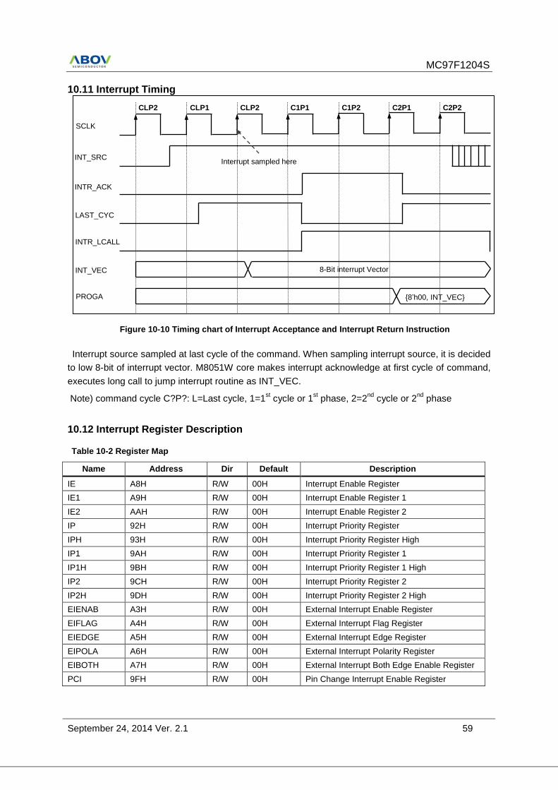
10.11 Interrupt Timing
Interrupt source sampled at last cycle of the command. When sampling interrupt source, it is decided
to low 8-bit of interrupt vector. M8051W core makes interrupt acknowledge at first cycle of command,
executes long call to jump interrupt routine as INT_VEC.
Note) command cycle C?P?: L=Last cycle, 1=1st cycle or 1
st phase, 2=2
nd cycle or 2
nd phase
10.12 Interrupt Register Description
Table 10-2 Register Map
Name Address Dir Default Description
IE A8H R/W 00H Interrupt Enable Register
IE1 A9H R/W 00H Interrupt Enable Register 1
IE2 AAH R/W 00H Interrupt Enable Register 2
IP 92H R/W 00H Interrupt Priority Register
IPH 93H R/W 00H Interrupt Priority Register High
IP1 9AH R/W 00H Interrupt Priority Register 1
IP1H 9BH R/W 00H Interrupt Priority Register 1 High
IP2 9CH R/W 00H Interrupt Priority Register 2
IP2H 9DH R/W 00H Interrupt Priority Register 2 High
EIENAB A3H R/W 00H External Interrupt Enable Register
EIFLAG A4H R/W 00H External Interrupt Flag Register
EIEDGE A5H R/W 00H External Interrupt Edge Register
EIPOLA A6H R/W 00H External Interrupt Polarity Register
EIBOTH A7H R/W 00H External Interrupt Both Edge Enable Register
PCI 9FH R/W 00H Pin Change Interrupt Enable Register
CLP2 CLP1 C2P1 C1P1 C2P2 C1P2 CLP2
Interrupt sampled here
8-Bit interrupt Vector
INT_SRC
INTR_ACK
LAST_CYC
INTR_LCALL
INT_VEC
PROGA
SCLK
{8’h00, INT_VEC}
Figure 10-10 Timing chart of Interrupt Acceptance and Interrupt Return Instruction
MC97F1204S
60 September 24, 2014 Ver. 2.1
10.12.1 Register description for Interrupt
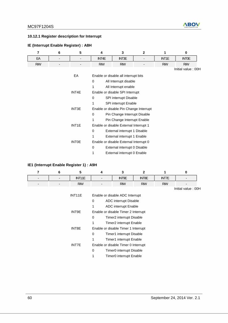
IE (Interrupt Enable Register) : A8H
7 6 5 4 3 2 1 0
EA - - INT4E INT3E - INT1E INT0E
R/W - - R/W R/W - R/W R/W
Initial value : 00H
EA Enable or disable all interrupt bits
0 All Interrupt disable
1 All Interrupt enable
INT4E Enable or disable SPI Interrupt
0 SPI interrupt Disable
1 SPI interrupt Enable
INT3E Enable or disable Pin Change Interrupt
0 Pin Change Interrupt Disable
1 Pin Change Interrupt Enable
INT1E Enable or disable External Interrupt 1
0 External interrupt 1 Disable
1 External interrupt 1 Enable
INT0E Enable or disable External Interrupt 0
0 External interrupt 0 Disable
1 External interrupt 0 Enable
IE1 (Interrupt Enable Register 1) : A9H
7 6 5 4 3 2 1 0
- - INT11E - INT9E INT8E INT7E -
- - R/W - R/W R/W R/W -
Initial value : 00H
INT11E Enable or disable ADC Interrupt
0 ADC interrupt Disable
1 ADC interrupt Enable
INT9E Enable or disable Timer 2 Interrupt
0 Timer2 interrupt Disable
1 Timer2 interrupt Enable
INT8E Enable or disable Timer 1 Interrupt
0 Timer1 interrupt Disable
1 Timer1 interrupt Enable
INT7E Enable or disable Timer 0 Interrupt
0 Timer0 interrupt Disable
1 Timer0 interrupt Enable
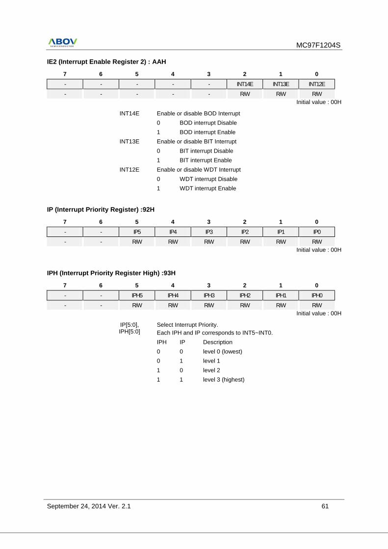
MC97F1204S
September 24, 2014 Ver. 2.1 61
IE2 (Interrupt Enable Register 2) : AAH
7 6 5 4 3 2 1 0
- - - - - INT14E INT13E INT12E
- - - - - R/W R/W R/W
Initial value : 00H
INT14E Enable or disable BOD Interrupt
0 BOD interrupt Disable
1 BOD interrupt Enable
INT13E Enable or disable BIT Interrupt
0 BIT interrupt Disable
1 BIT interrupt Enable
INT12E Enable or disable WDT Interrupt
0 WDT interrupt Disable
1 WDT interrupt Enable
IP (Interrupt Priority Register) :92H
7 6 5 4 3 2 1 0
- - IP5 IP4 IP3 IP2 IP1 IP0
- - R/W R/W R/W R/W R/W R/W
Initial value : 00H
IPH (Interrupt Priority Register High) :93H
7 6 5 4 3 2 1 0
- - IPH5 IPH4 IPH3 IPH2 IPH1 IPH0
- - R/W R/W R/W R/W R/W R/W
Initial value : 00H
IP[5:0], IPH[5:0]
Select Interrupt Priority.
Each IPH and IP corresponds to INT5~INT0.
IPH IP Description
0 0 level 0 (lowest)
0 1 level 1
1 0 level 2
1 1 level 3 (highest)
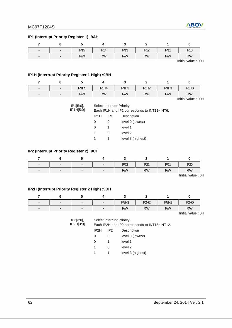
MC97F1204S
62 September 24, 2014 Ver. 2.1
IP1 (Interrupt Priority Register 1) :9AH
7 6 5 4 3 2 1 0
- - IP15 IP14 IP13 IP12 IP11 IP10
- - R/W R/W R/W R/W R/W R/W
Initial value : 00H
IP1H (Interrupt Priority Register 1 High) :9BH
7 6 5 4 3 2 1 0
- - IP1H5 IP1H4 IP1H3 IP1H2 IP1H1 IP1H0
- - R/W R/W R/W R/W R/W R/W
Initial value : 00H
IP1[5:0], IP1H[5:0]
Select Interrupt Priority.
Each IP1H and IP1 corresponds to INT11~INT6.
IP1H IP1 Description
0 0 level 0 (lowest)
0 1 level 1
1 0 level 2
1 1 level 3 (highest)
IP2 (Interrupt Priority Register 2) :9CH
7 6 5 4 3 2 1 0
- - - - IP23 IP22 IP21 IP20
- - - - R/W R/W R/W R/W
Initial value : 0H
IP2H (Interrupt Priority Register 2 High) :9DH
7 6 5 4 3 2 1 0
- - - - IP2H3 IP2H2 IP2H1 IP2H0
- - - - R/W R/W R/W R/W
Initial value : 0H
IP2[3:0], IP2H[3:0]
Select Interrupt Priority.
Each IP2H and IP2 corresponds to INT15~INT12.
IP2H IP2 Description
0 0 level 0 (lowest)
0 1 level 1
1 0 level 2
1 1 level 3 (highest)
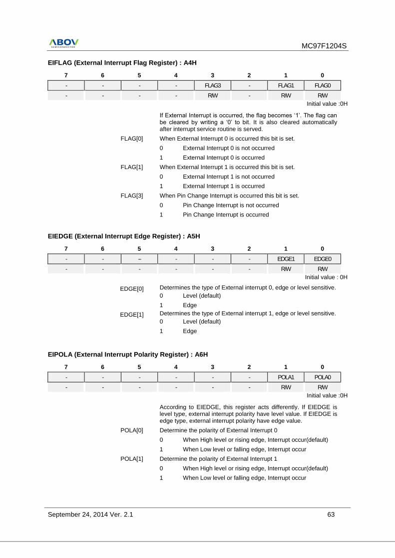
MC97F1204S
September 24, 2014 Ver. 2.1 63
EIFLAG (External Interrupt Flag Register) : A4H
7 6 5 4 3 2 1 0
- - - - FLAG3 - FLAG1 FLAG0
- - - - R/W - R/W R/W
Initial value :0H
If External Interrupt is occurred, the flag becomes ‘1’. The flag can be cleared by writing a ‘0’ to bit. It is also cleared automatically after interrupt service routine is served.
FLAG[0] When External Interrupt 0 is occurred this bit is set.
0 External Interrupt 0 is not occurred
1 External Interrupt 0 is occurred
FLAG[1] When External Interrupt 1 is occurred this bit is set.
0 External Interrupt 1 is not occurred
1 External Interrupt 1 is occurred
FLAG[3] When Pin Change Interrupt is occurred this bit is set.
0 Pin Change Interrupt is not occurred
1 Pin Change Interrupt is occurred
EIEDGE (External Interrupt Edge Register) : A5H
7 6 5 4 3 2 1 0
- - -- - - - EDGE1 EDGE0
- - - - - - R/W R/W
Initial value : 0H
EDGE[0] Determines the type of External interrupt 0, edge or level sensitive.
0 Level (default)
1 Edge
EDGE[1] Determines the type of External interrupt 1, edge or level sensitive.
0 Level (default)
1 Edge
EIPOLA (External Interrupt Polarity Register) : A6H
7 6 5 4 3 2 1 0
- - - - - - POLA1 POLA0
- - - - - - R/W R/W
Initial value :0H
According to EIEDGE, this register acts differently. If EIEDGE is level type, external interrupt polarity have level value. If EIEDGE is edge type, external interrupt polarity have edge value.
POLA[0] Determine the polarity of External Interrupt 0
0 When High level or rising edge, Interrupt occur(default)
1 When Low level or falling edge, Interrupt occur
POLA[1] Determine the polarity of External Interrupt 1
0 When High level or rising edge, Interrupt occur(default)
1 When Low level or falling edge, Interrupt occur
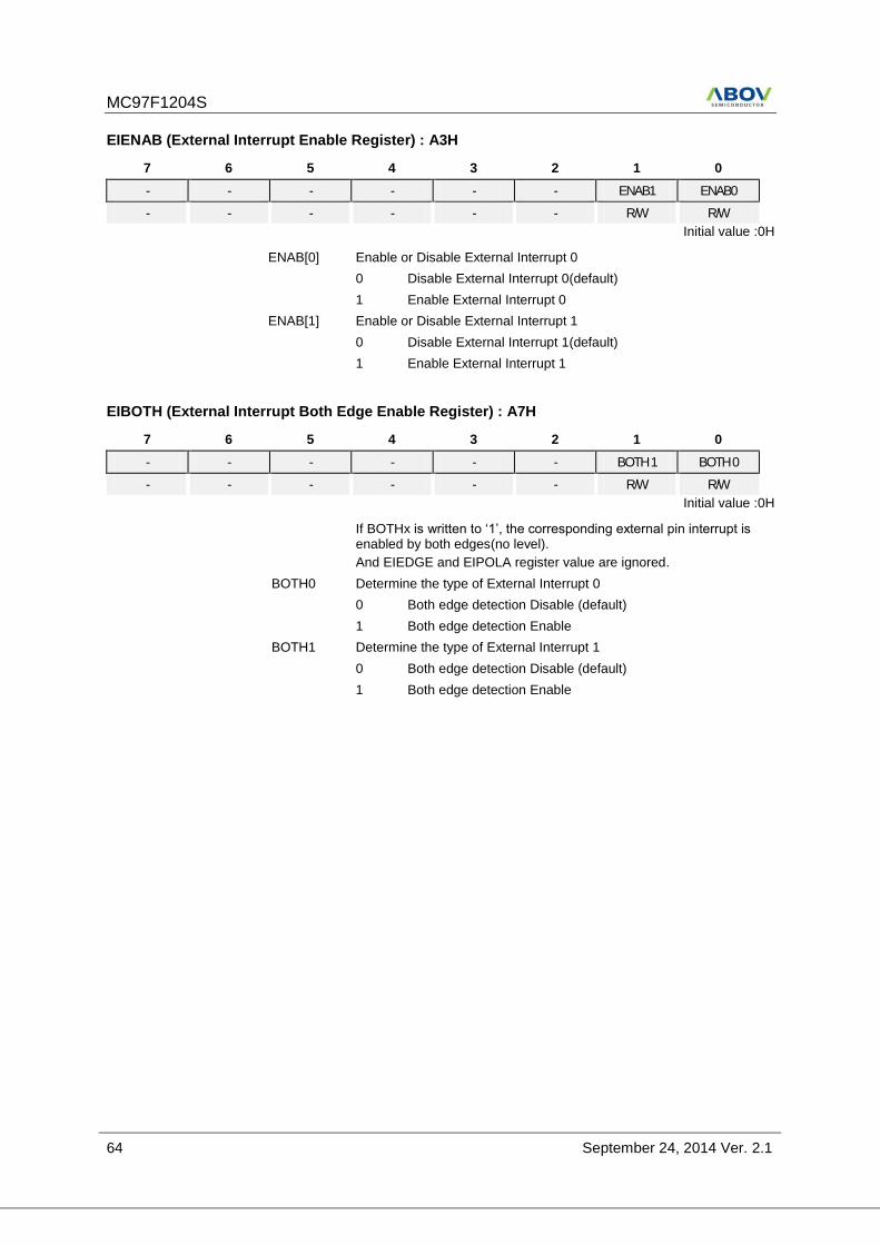
MC97F1204S
64 September 24, 2014 Ver. 2.1
EIENAB (External Interrupt Enable Register) : A3H
7 6 5 4 3 2 1 0
- - - - - - ENAB1 ENAB0
- - - - - - R/W R/W
Initial value :0H
ENAB[0] Enable or Disable External Interrupt 0
0 Disable External Interrupt 0(default)
1 Enable External Interrupt 0
ENAB[1] Enable or Disable External Interrupt 1
0 Disable External Interrupt 1(default)
1 Enable External Interrupt 1
EIBOTH (External Interrupt Both Edge Enable Register) : A7H
7 6 5 4 3 2 1 0
- - - - - - BOTH 1 BOTH 0
- - - - - - R/W R/W
Initial value :0H
If BOTHx is written to ‘1’, the corresponding external pin interrupt is enabled by both edges(no level).
And EIEDGE and EIPOLA register value are ignored.
BOTH0 Determine the type of External Interrupt 0
0 Both edge detection Disable (default)
1 Both edge detection Enable
BOTH1 Determine the type of External Interrupt 1
0 Both edge detection Disable (default)
1 Both edge detection Enable
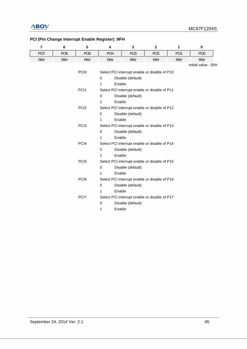
MC97F1204S
September 24, 2014 Ver. 2.1 65
PCI (Pin Change Interrupt Enable Register) :9FH
7 6 5 4 3 2 1 0
PCI7 PCI6 PCI5 PCI4 PCI3 PCI2 PCI1 PCI0
R/W R/W R/W R/W R/W R/W R/W R/W
Initial value : 00H
PCI0 Select PCI interrupt enable or disable of P10
0 Disable (default)
1 Enable
PCI1 Select PCI interrupt enable or disable of P11
0 Disable (default)
1 Enable
PCI2 Select PCI interrupt enable or disable of P12
0 Disable (default)
1 Enable
PCI3 Select PCI interrupt enable or disable of P13
0 Disable (default)
1 Enable
PCI4 Select PCI interrupt enable or disable of P14
0 Disable (default)
1 Enable
PCI5 Select PCI interrupt enable or disable of P15
0 Disable (default)
1 Enable
PCI6 Select PCI interrupt enable or disable of P16
0 Disable (default)
1 Enable
PCI7 Select PCI interrupt enable or disable of P17
0 Disable (default)
1 Enable
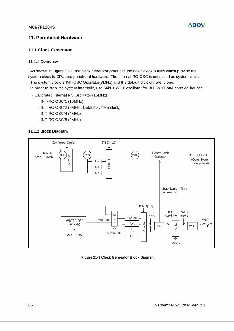
MC97F1204S
66 September 24, 2014 Ver. 2.1
11. Peripheral Hardware
11.1 Clock Generator
11.1.1 Overview
As shown in Figure 11-1, the clock generator produces the basic clock pulses which provide the
system clock to CPU and peripheral hardware. The internal RC-OSC is only used as system clock.
The system clock is INT-OSC Oscillator(8MHz) and the default division rate is one.
In order to stabilize system internally, use 64kHz WDT-oscillator for BIT, WDT and ports de-bounce.
- Calibrated Internal RC Oscillator (16MHz)
. INT-RC OSC/1 (16MHz)
. INT-RC OSC/2 (8MHz , Default system clock)
. INT-RC OSC/4 (4MHz)
. INT-RC OSC/8 (2MHz)
11.1.2 Block Diagram
SCLK=fX
(Core, System, Peripheral)
MUX
INT-OSC16/8/4/2 (MHz)
SYSCK[1:0]
1/4
1/8
fIRC
Configure Option
1/2
WDTRC-OSC(64KHz)
WDTRCON
BITclock
Stabilization TimeGeneration
BIToverflow
WDToverflow
WDTCK
WDTclock
BITWDTRC
fWDTRC
fSYS
BITCK[1:0]
1/256
1/16
MUX
fXIN
BIT
System ClockGenerator
MUX
WDT
1/2048
MUX
1/2
MUX
Figure 11-1 Clock Generator Block Diagram
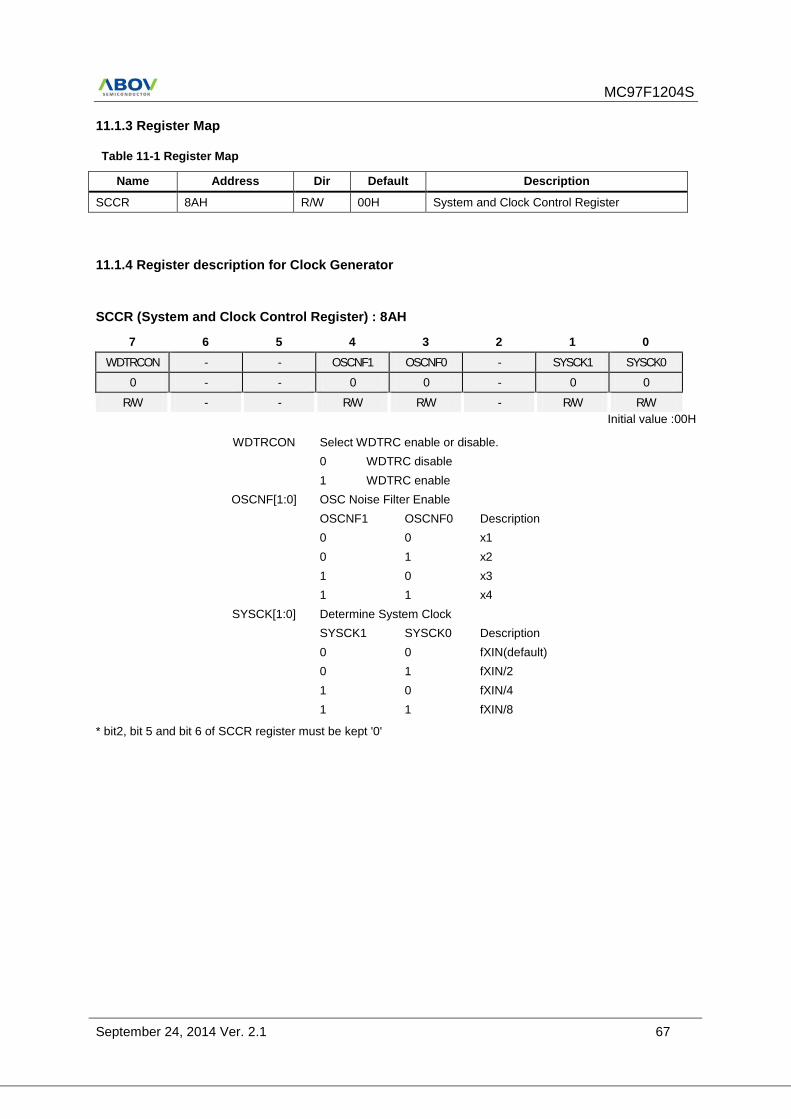
MC97F1204S
September 24, 2014 Ver. 2.1 67
11.1.3 Register Map
Table 11-1 Register Map
Name Address Dir Default Description
SCCR 8AH R/W 00H System and Clock Control Register
11.1.4 Register description for Clock Generator
SCCR (System and Clock Control Register) : 8AH
7 6 5 4 3 2 1 0
WDTRCON - - OSCNF1 OSCNF0 - SYSCK1 SYSCK0
0 - - 0 0 - 0 0
R/W - - R/W R/W - R/W R/W
Initial value :00H
WDTRCON Select WDTRC enable or disable.
0 WDTRC disable
1 WDTRC enable
OSCNF[1:0] OSC Noise Filter Enable
OSCNF1 OSCNF0 Description
0 0 x1
0 1 x2
1 0 x3
1 1 x4
SYSCK[1:0] Determine System Clock
SYSCK1 SYSCK0 Description
0 0 fXIN(default)
0 1 fXIN/2
1 0 fXIN/4
1 1 fXIN/8
* bit2, bit 5 and bit 6 of SCCR register must be kept '0'
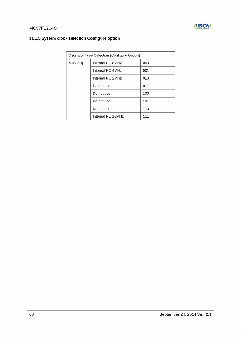
MC97F1204S
68 September 24, 2014 Ver. 2.1
11.1.5 System clock selection Configure option
Oscillator Type Selection (Configure Option)
XTS[2:0] Internal RC 8MHz 000
Internal RC 4MHz 001
Internal RC 2MHz 010
Do not use 011
Do not use 100
Do not use 101
Do not use 110
Internal RC 16MHz 111
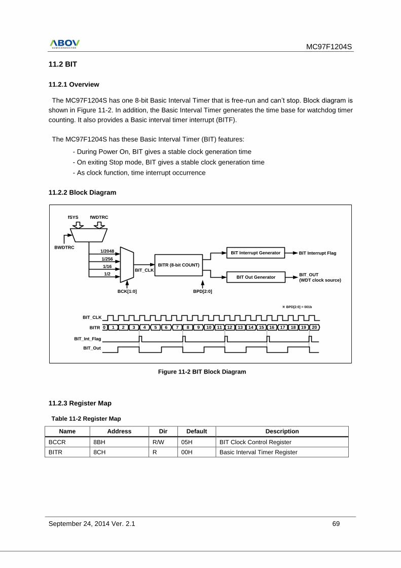
MC97F1204S
September 24, 2014 Ver. 2.1 69
11.2 BIT
11.2.1 Overview
The MC97F1204S has one 8-bit Basic Interval Timer that is free-run and can’t stop. Block diagram is
shown in Figure 11-2. In addition, the Basic Interval Timer generates the time base for watchdog timer
counting. It also provides a Basic interval timer interrupt (BITF).
The MC97F1204S has these Basic Interval Timer (BIT) features:
- During Power On, BIT gives a stable clock generation time
- On exiting Stop mode, BIT gives a stable clock generation time
- As clock function, time interrupt occurrence
11.2.2 Block Diagram
BITR (8-bit COUNT)BIT_CLK
BIT Interrupt Generator
BIT Out Generator
BIT Interrupt Flag
BIT_OUT
(WDT clock source)
BIT_CLK
0 1 2 3 4 5 6 7 8 9 10 11 12 13 14 15 16 17 18 19 20BITR
BIT_Int_Flag
BIT_Out
※ BPD[2:0] = 001b
BCK[1:0] BPD[2:0]
1/2048
1/256
1/16
1/2
fSYS fWDTRC
BWDTRC
Figure 11-2 BIT Block Diagram
11.2.3 Register Map
Table 11-2 Register Map
Name Address Dir Default Description
BCCR 8BH R/W 05H BIT Clock Control Register
BITR 8CH R 00H Basic Interval Timer Register
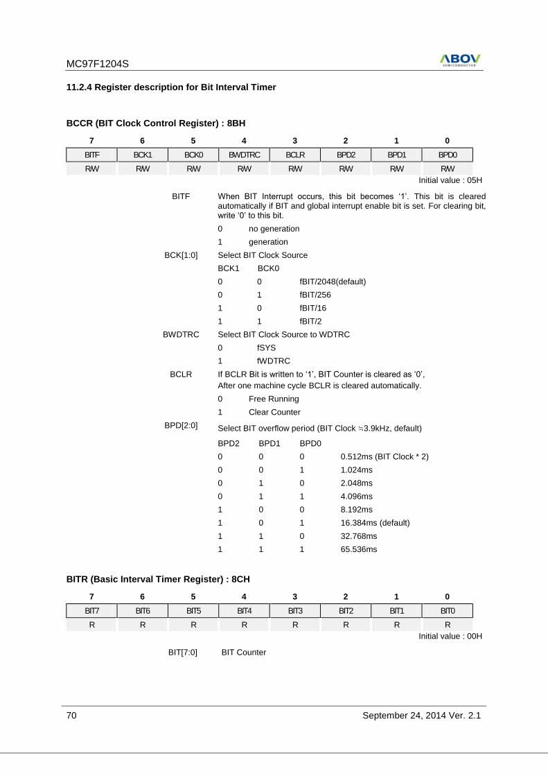
MC97F1204S
70 September 24, 2014 Ver. 2.1
11.2.4 Register description for Bit Interval Timer
BCCR (BIT Clock Control Register) : 8BH
7 6 5 4 3 2 1 0
BITF BCK1 BCK0 BWDTRC BCLR BPD2 BPD1 BPD0
R/W R/W R/W R/W R/W R/W R/W R/W
Initial value : 05H
BITF When BIT Interrupt occurs, this bit becomes ‘1’. This bit is cleared automatically if BIT and global interrupt enable bit is set. For clearing bit, write ‘0’ to this bit.
0 no generation
1 generation
BCK[1:0] Select BIT Clock Source
BCK1 BCK0
0 0 fBIT/2048(default)
0 1 fBIT/256
1 0 fBIT/16
1 1 fBIT/2
BWDTRC Select BIT Clock Source to WDTRC
0 fSYS
1 fWDTRC
BCLR If BCLR Bit is written to ‘1’, BIT Counter is cleared as ‘0’,
After one machine cycle BCLR is cleared automatically.
0 Free Running
1 Clear Counter
BPD[2:0] Select BIT overflow period (BIT Clock ≒3.9kHz, default)
BPD2 BPD1 BPD0
0 0 0 0.512ms (BIT Clock * 2)
0 0 1 1.024ms
0 1 0 2.048ms
0 1 1 4.096ms
1 0 0 8.192ms
1 0 1 16.384ms (default)
1 1 0 32.768ms
1 1 1 65.536ms
BITR (Basic Interval Timer Register) : 8CH
7 6 5 4 3 2 1 0
BIT7 BIT6 BIT5 BIT4 BIT3 BIT2 BIT1 BIT0
R R R R R R R R
Initial value : 00H
BIT[7:0] BIT Counter
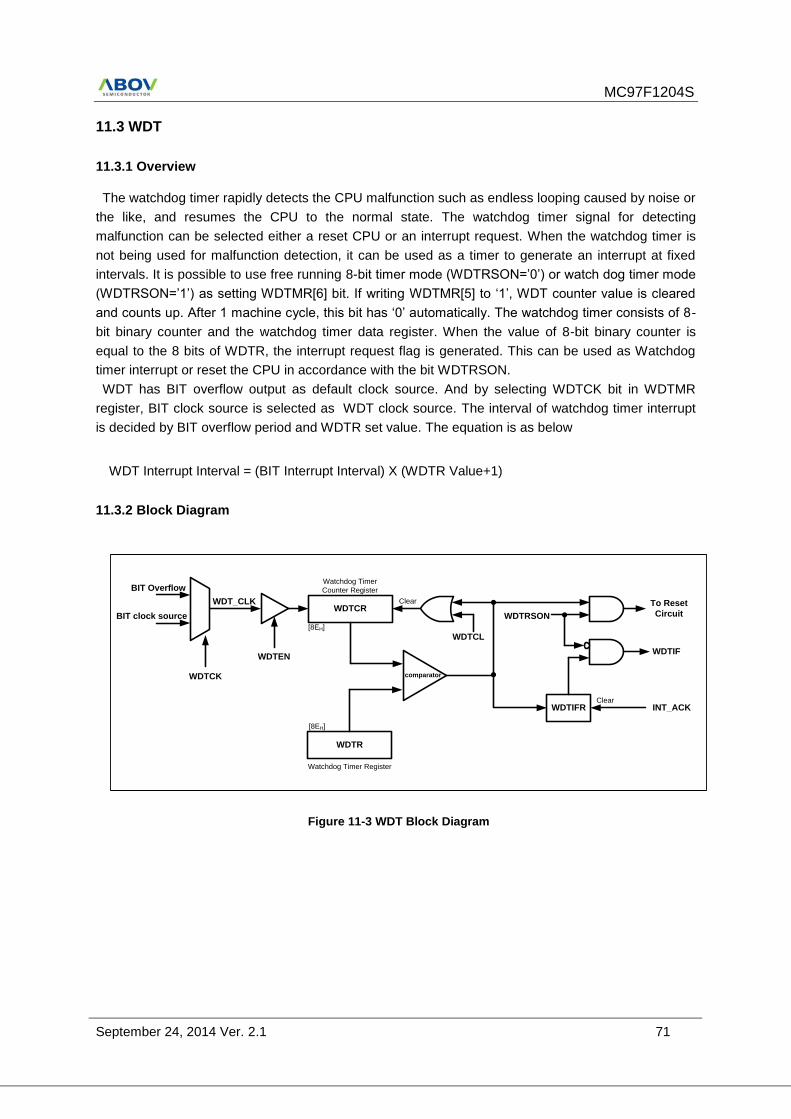
MC97F1204S
September 24, 2014 Ver. 2.1 71
11.3 WDT
11.3.1 Overview
The watchdog timer rapidly detects the CPU malfunction such as endless looping caused by noise or
the like, and resumes the CPU to the normal state. The watchdog timer signal for detecting
malfunction can be selected either a reset CPU or an interrupt request. When the watchdog timer is
not being used for malfunction detection, it can be used as a timer to generate an interrupt at fixed
intervals. It is possible to use free running 8-bit timer mode (WDTRSON=’0’) or watch dog timer mode
(WDTRSON=’1’) as setting WDTMR[6] bit. If writing WDTMR[5] to ‘1’, WDT counter value is cleared
and counts up. After 1 machine cycle, this bit has ‘0’ automatically. The watchdog timer consists of 8-
bit binary counter and the watchdog timer data register. When the value of 8-bit binary counter is
equal to the 8 bits of WDTR, the interrupt request flag is generated. This can be used as Watchdog
timer interrupt or reset the CPU in accordance with the bit WDTRSON.
WDT has BIT overflow output as default clock source. And by selecting WDTCK bit in WDTMR
register, BIT clock source is selected as WDT clock source. The interval of watchdog timer interrupt
is decided by BIT overflow period and WDTR set value. The equation is as below
WDT Interrupt Interval = (BIT Interrupt Interval) X (WDTR Value+1)
11.3.2 Block Diagram
BIT Overflow
WDTCR
Watchdog Timer
Counter Register
WDTR
[8EH]
[8EH]
comparator
Watchdog Timer Register
Clear
WDTCL
WDTRSON
WDTIFRClear
INT_ACK
WDTIF
To Reset
Circuit
WDT_CLK
BIT clock source
WDTCK
WDTEN
Figure 11-3 WDT Block Diagram
MC97F1204S
72 September 24, 2014 Ver. 2.1
11.3.3 Register Map
Table 11-3 Register Map
Name Address Dir Default Description
WDTR 8EH W FFH Watch Dog Timer Register
WDTCR 8EH R 00H Watch Dog Timer Counter Register
WDTMR 8DH R/W 00H Watch Dog Timer Mode Register
11.3.4 Register description for Watch Dog Timer
WDTR (Watch Dog Timer Register: Write Case) : 8EH
7 6 5 4 3 2 1 0
WDTR7 WDTR6 WDTR5 WDTR4 WDTR3 WDTR2 WDTR1 WDTR0
W W W W W W W W
Initial value : FFH
WDTR[7:0] Set a period
WDT Interrupt Interval=(BIT Interrupt Interval) x(WDTR Value+1)
Note) To guarantee proper operation, the data should be greater than 01H.
WDTCR (Watch Dog Timer Counter Register: Read Case) : 8EH
7 6 5 4 3 2 1 0
WDTCR7 WDTCR6 WDTCR5 WDTCR4 WDTCR3 WDTCR2 WDTCR1 WDTCR0
R R R R R R R R
Initial value : 00H
WDTCR[7:0] WDT Counter
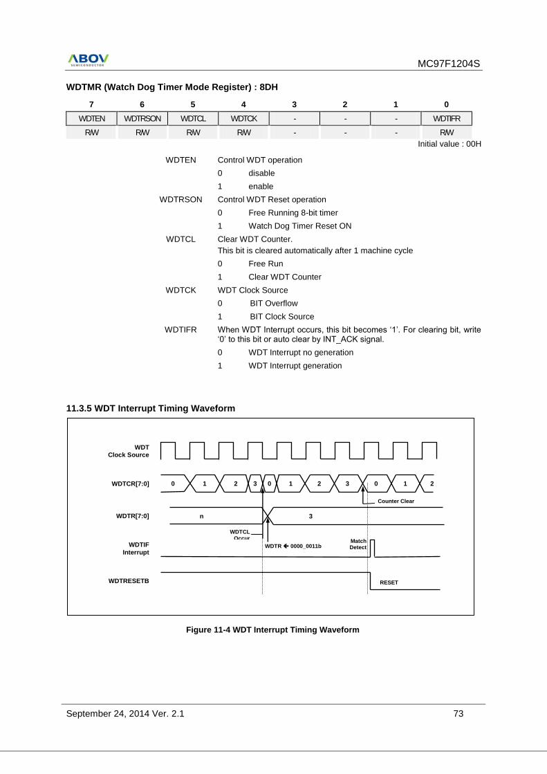
MC97F1204S
September 24, 2014 Ver. 2.1 73
WDTMR (Watch Dog Timer Mode Register) : 8DH
7 6 5 4 3 2 1 0
WDTEN WDTRSON WDTCL WDTCK - - - WDTIFR
R/W R/W R/W R/W - - - R/W
Initial value : 00H
WDTEN Control WDT operation
0 disable
1 enable
WDTRSON Control WDT Reset operation
0 Free Running 8-bit timer
1 Watch Dog Timer Reset ON
WDTCL Clear WDT Counter.
This bit is cleared automatically after 1 machine cycle
0 Free Run
1 Clear WDT Counter
WDTCK WDT Clock Source
0 BIT Overflow
1 BIT Clock Source
WDTIFR When WDT Interrupt occurs, this bit becomes ‘1’. For clearing bit, write ‘0’ to this bit or auto clear by INT_ACK signal.
0 WDT Interrupt no generation
1 WDT Interrupt generation
11.3.5 WDT Interrupt Timing Waveform
WDT Clock Source
WDTCR[7:0]
WDTR[7:0]
WDTIF
Interrupt
WDTRESETB
WDTCL Occur
WDTR 0000_0011b Match Detect
Counter Clear
RESET
0 1 2 3 0 1 2 3 0 1 2
n 3
Figure 11-4 WDT Interrupt Timing Waveform
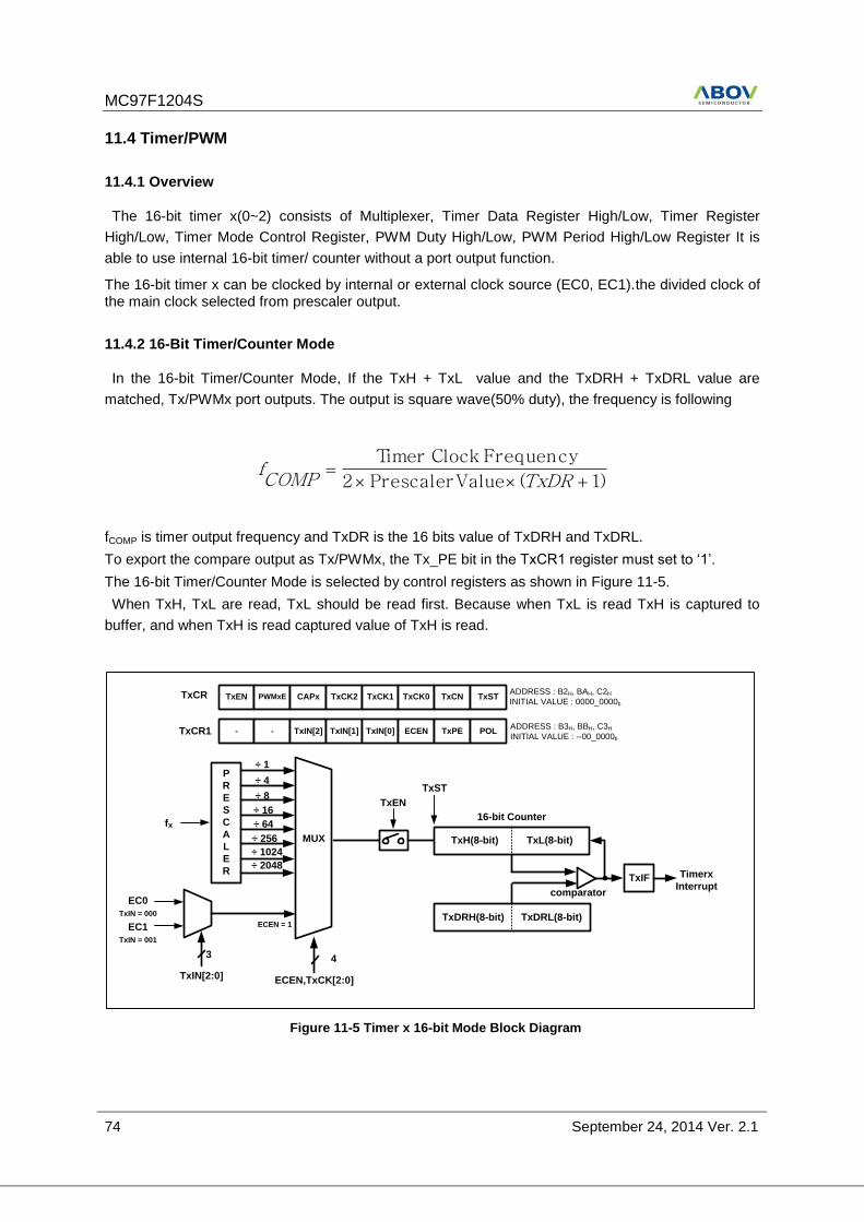
MC97F1204S
74 September 24, 2014 Ver. 2.1
11.4 Timer/PWM
11.4.1 Overview
The 16-bit timer x(0~2) consists of Multiplexer, Timer Data Register High/Low, Timer Register
High/Low, Timer Mode Control Register, PWM Duty High/Low, PWM Period High/Low Register It is
able to use internal 16-bit timer/ counter without a port output function.
The 16-bit timer x can be clocked by internal or external clock source (EC0, EC1).the divided clock of the main clock selected from prescaler output.
11.4.2 16-Bit Timer/Counter Mode
In the 16-bit Timer/Counter Mode, If the TxH + TxL value and the TxDRH + TxDRL value are
matched, Tx/PWMx port outputs. The output is square wave(50% duty), the frequency is following
)1(Value Prescaler2
Frequency Clock Timer
TxDRCOMPf
fCOMP is timer output frequency and TxDR is the 16 bits value of TxDRH and TxDRL.
To export the compare output as Tx/PWMx, the Tx_PE bit in the TxCR1 register must set to ‘1’.
The 16-bit Timer/Counter Mode is selected by control registers as shown in Figure 11-5.
When TxH, TxL are read, TxL should be read first. Because when TxL is read TxH is captured to
buffer, and when TxH is read captured value of TxH is read.
P
R
E
S
C
A
L
E
R
÷ 1
÷ 4
÷ 8
÷ 16
÷ 64
÷ 256
÷ 1024
÷ 2048
MUX TxH(8-bit) TxL(8-bit)
16-bit Counter
TxST
TxEN
4
ECEN,TxCK[2:0]
fX
TxIF Timerx
Interrupt
- - TxIN[2] TxIN[1] TxIN[0] ECEN TxPE POL
TxCR
TxCR1
ADDRESS : B2H, BAH, C2H
INITIAL VALUE : 0000_0000b
ADDRESS : B3H, BBH, C3H
INITIAL VALUE : --00_0000b
comparator
TxDRH(8-bit) TxDRL(8-bit)
TxEN PWMxE CAPx TxCK2 TxCK1 TxCK0 TxCN TxST
EC0
TxIN = 000
EC1
TxIN = 001
3
TxIN[2:0]
ECEN = 1
Figure 11-5 Timer x 16-bit Mode Block Diagram
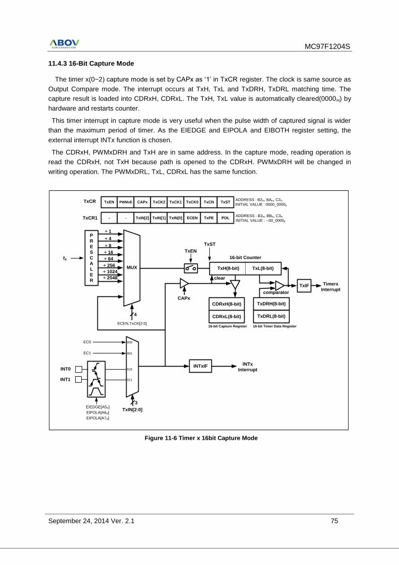
MC97F1204S
September 24, 2014 Ver. 2.1 75
11.4.3 16-Bit Capture Mode
The timer x(0~2) capture mode is set by CAPx as ‘1’ in TxCR register. The clock is same source as
Output Compare mode. The interrupt occurs at TxH, TxL and TxDRH, TxDRL matching time. The
capture result is loaded into CDRxH, CDRxL. The TxH, TxL value is automatically cleared(0000H) by
hardware and restarts counter.
This timer interrupt in capture mode is very useful when the pulse width of captured signal is wider
than the maximum period of timer. As the EIEDGE and EIPOLA and EIBOTH register setting, the
external interrupt INTx function is chosen.
The CDRxH, PWMxDRH and TxH are in same address. In the capture mode, reading operation is
read the CDRxH, not TxH because path is opened to the CDRxH. PWMxDRH will be changed in
writing operation. The PWMxDRL, TxL, CDRxL has the same function.
P
R
E
S
C
A
L
E
R
÷ 1
÷ 4
÷ 8
÷ 16
÷ 64
÷ 256
÷ 1024
÷ 2048
MUX TxH(8-bit) TxL(8-bit)
16-bit Counter
TxST
TxEN
4
ECEN,TxCK[2:0]
fX
TxIF Timerx
Interrupt
- - TxIN[2] TxIN[1] TxIN[0] ECEN TxPE POL
TxCR
TxCR1
ADDRESS : B2H, BAH, C2H
INITIAL VALUE : 0000_0000b
ADDRESS : B3H, BBH, C3H
INITIAL VALUE : --00_0000b
comparator
TxDRH(8-bit)
TxEN PWMxE CAPx TxCK2 TxCK1 TxCK0 TxCN TxST
EC0
EC1
3
TxDRL(8-bit)
CDRxH(8-bit)
CDRxL(8-bit)
clear
INT0
INT1
EIEDGE[A5H]
EIPOLA[A6H]
EIPOLA[A7H]
16-bit Capture Register 16-bit Timer Data Register
INTxIF INTx
Interrupt
TxIN[2:0]
010
011
CAPx
000
001
Figure 11-6 Timer x 16bit Capture Mode
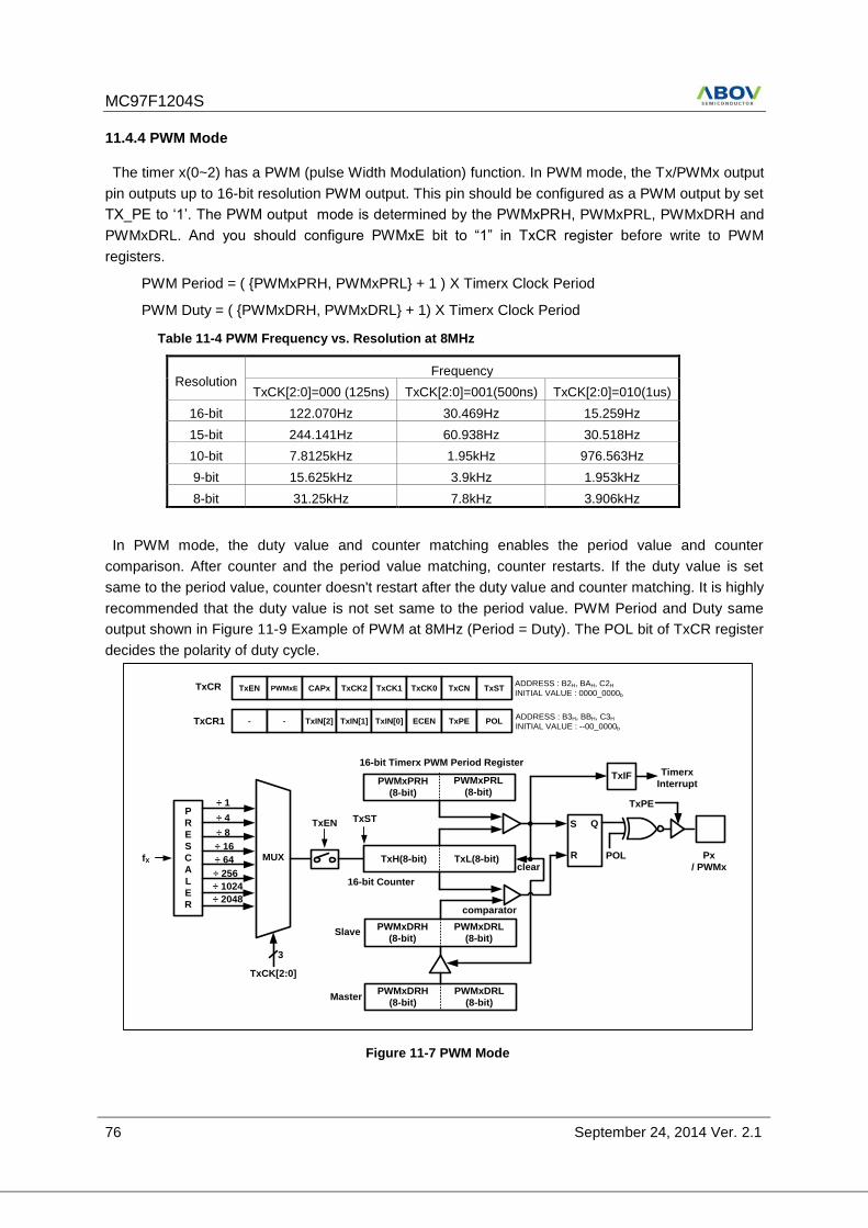
MC97F1204S
76 September 24, 2014 Ver. 2.1
11.4.4 PWM Mode
The timer x(0~2) has a PWM (pulse Width Modulation) function. In PWM mode, the Tx/PWMx output
pin outputs up to 16-bit resolution PWM output. This pin should be configured as a PWM output by set
TX_PE to ‘1’. The PWM output mode is determined by the PWMxPRH, PWMxPRL, PWMxDRH and
PWMxDRL. And you should configure PWMxE bit to “1” in TxCR register before write to PWM
registers.
PWM Period = ( {PWMxPRH, PWMxPRL} + 1 ) X Timerx Clock Period
PWM Duty = ( {PWMxDRH, PWMxDRL} + 1) X Timerx Clock Period
Table 11-4 PWM Frequency vs. Resolution at 8MHz
Resolution Frequency
TxCK[2:0]=000 (125ns) TxCK[2:0]=001(500ns) TxCK[2:0]=010(1us)
16-bit 122.070Hz 30.469Hz 15.259Hz
15-bit 244.141Hz 60.938Hz 30.518Hz
10-bit 7.8125kHz 1.95kHz 976.563Hz
9-bit 15.625kHz 3.9kHz 1.953kHz
8-bit 31.25kHz 7.8kHz 3.906kHz
In PWM mode, the duty value and counter matching enables the period value and counter
comparison. After counter and the period value matching, counter restarts. If the duty value is set
same to the period value, counter doesn't restart after the duty value and counter matching. It is highly
recommended that the duty value is not set same to the period value. PWM Period and Duty same
output shown in Figure 11-9 Example of PWM at 8MHz (Period = Duty). The POL bit of TxCR register
decides the polarity of duty cycle.
P
R
E
S
C
A
L
E
R
÷ 1
÷ 4
÷ 8
÷ 16
÷ 64
÷ 256
÷ 1024
÷ 2048
MUX TxH(8-bit) TxL(8-bit)
TxSTTxEN
3
TxCK[2:0]
fX
TxIF Timerx
Interrupt
- - TxIN[2] TxIN[1] TxIN[0] ECEN TxPE POL
TxCR
TxCR1
ADDRESS : B2H, BAH, C2H
INITIAL VALUE : 0000_0000b
ADDRESS : B3H, BBH, C3H
INITIAL VALUE : --00_0000b
comparator
PWMxDRH
(8-bit)
PWMxDRL
(8-bit)
TxEN PWMxE CAPx TxCK2 TxCK1 TxCK0 TxCN TxST
16-bit Counter
PWMxPRH
(8-bit)
PWMxPRL
(8-bit)
PWMxDRH
(8-bit)
PWMxDRL
(8-bit)
Slave
Master
S
R
Q
clear
POL
TxPE
Px
/ PWMx
16-bit Timerx PWM Period Register
Figure 11-7 PWM Mode
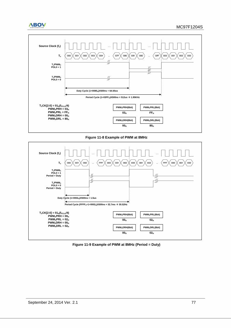
MC97F1204S
September 24, 2014 Ver. 2.1 77
PWMXPRH(8bit)
03H
Source Clock (fx)
0000 0001 0002 0003 0004 ... 007F 0080 0081 0082 ... 03FF 0000 0001 0002 0003
... ...
Tx
Tx/PWMX
POL0 = 1
Tx/PWMX
POL0 = 0
Duty Cycle (1+0080H)X500ns = 64.50us
Period Cycle (1+03FFH)X500ns = 512us à 1.95KHz
TXCK[2:0] = 01H(fPCLK/4)
PWMXPRH = 03H
PWMXPRL = FFH
PWMXDRH = 00H
PWMXDRL = 80H
PWMXPRL(8bit)
PWMXDRH(8bit) PWMXDRL(8bit)
FFH
00H 80H
Figure 11-8 Example of PWM at 8MHz
PWMXPRH(8bit)
00H
Source Clock (fx)
0000 0001 0002 ... FFFF 0000 0001 0002 0000 0001 0002 ... FFFF 0000 0001 0002
... ...
Tx
Tx/PWMX
POL0 = 1
Period = Duty
Tx/PWMX
POL0 = 0
Period = Duty
Duty Cycle (1+0002H)X500ns = 1.5us
Period Cycle (FFFFH+1+0002H)X500ns = 32.7ms à 30.52Hz
TXCK[2:0] = 01H(fPCLK/4)
PWMXPRH = 00H
PWMXPRL = 02H
PWMXDRH = 00H
PWMXDRL = 02H
PWMXPRL(8bit)
PWMXDRH(8bit) PWMXDRL(8bit)
02H
00H 02H
Figure 11-9 Example of PWM at 8MHz (Period = Duty)
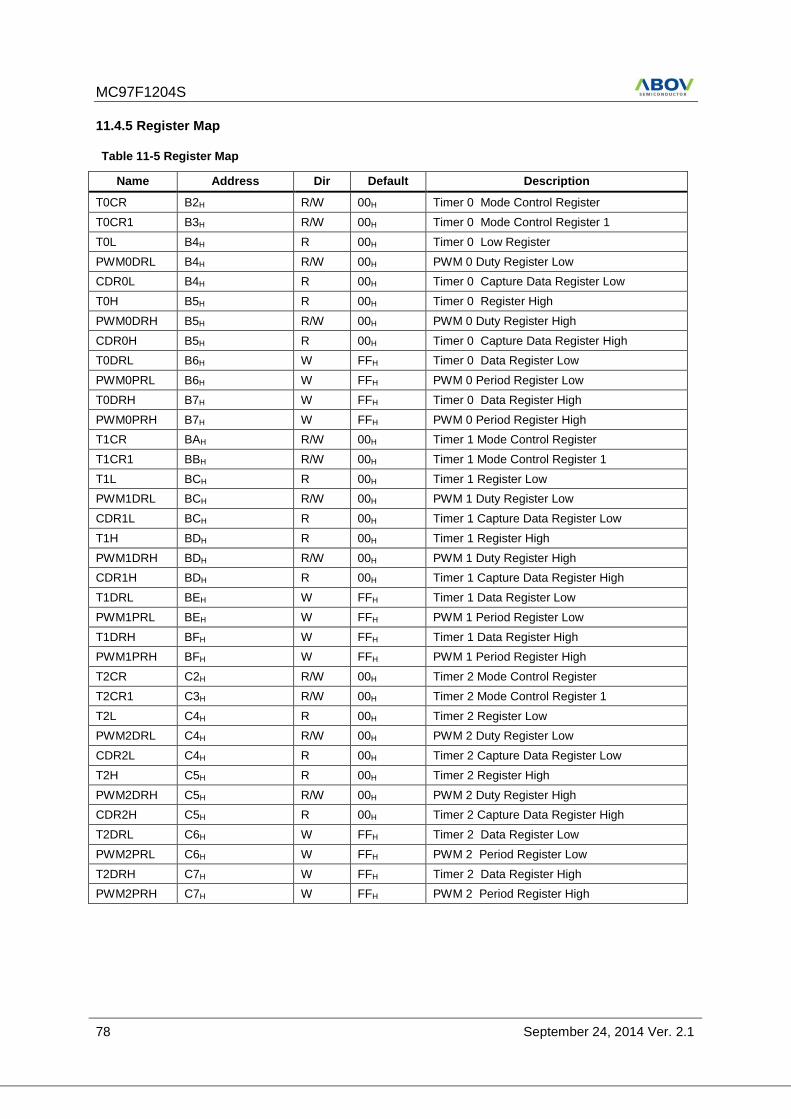
MC97F1204S
78 September 24, 2014 Ver. 2.1
11.4.5 Register Map
Table 11-5 Register Map
Name Address Dir Default Description
T0CR B2H R/W 00H Timer 0 Mode Control Register
T0CR1 B3H R/W 00H Timer 0 Mode Control Register 1
T0L B4H R 00H Timer 0 Low Register
PWM0DRL B4H R/W 00H PWM 0 Duty Register Low
CDR0L B4H R 00H Timer 0 Capture Data Register Low
T0H B5H R 00H Timer 0 Register High
PWM0DRH B5H R/W 00H PWM 0 Duty Register High
CDR0H B5H R 00H Timer 0 Capture Data Register High
T0DRL B6H W FFH Timer 0 Data Register Low
PWM0PRL B6H W FFH PWM 0 Period Register Low
T0DRH B7H W FFH Timer 0 Data Register High
PWM0PRH B7H W FFH PWM 0 Period Register High
T1CR BAH R/W 00H Timer 1 Mode Control Register
T1CR1 BBH R/W 00H Timer 1 Mode Control Register 1
T1L BCH R 00H Timer 1 Register Low
PWM1DRL BCH R/W 00H PWM 1 Duty Register Low
CDR1L BCH R 00H Timer 1 Capture Data Register Low
T1H BDH R 00H Timer 1 Register High
PWM1DRH BDH R/W 00H PWM 1 Duty Register High
CDR1H BDH R 00H Timer 1 Capture Data Register High
T1DRL BEH W FFH Timer 1 Data Register Low
PWM1PRL BEH W FFH PWM 1 Period Register Low
T1DRH BFH W FFH Timer 1 Data Register High
PWM1PRH BFH W FFH PWM 1 Period Register High
T2CR C2H R/W 00H Timer 2 Mode Control Register
T2CR1 C3H R/W 00H Timer 2 Mode Control Register 1
T2L C4H R 00H Timer 2 Register Low
PWM2DRL C4H R/W 00H PWM 2 Duty Register Low
CDR2L C4H R 00H Timer 2 Capture Data Register Low
T2H C5H R 00H Timer 2 Register High
PWM2DRH C5H R/W 00H PWM 2 Duty Register High
CDR2H C5H R 00H Timer 2 Capture Data Register High
T2DRL C6H W FFH Timer 2 Data Register Low
PWM2PRL C6H W FFH PWM 2 Period Register Low
T2DRH C7H W FFH Timer 2 Data Register High
PWM2PRH C7H W FFH PWM 2 Period Register High
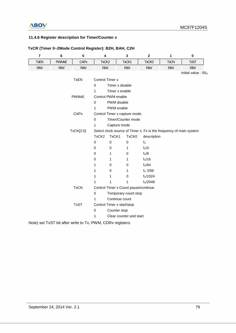
MC97F1204S
September 24, 2014 Ver. 2.1 79
11.4.6 Register description for Timer/Counter x
TxCR (Timer 0~2Mode Control Register): B2H, BAH, C2H
7 6 5 4 3 2 1 0
TxEN PWMxE CAPx TxCK2 TxCK1 TxCK0 TxCN TxST
R/W R/W R/W R/W R/W R/W R/W R/W
Initial value : 00H
TxEN Control Timer x
0 Timer x disable
1 Timer x enable
PWMxE Control PWM enable
0 PWM disable
1 PWM enable
CAPx Control Timer x capture mode.
0 Timer/Counter mode
1 Capture mode
TxCK[2:0] Select clock source of Timer x. Fx is the frequency of main system
TxCK2 TxCK1 TxCK0 description
0 0 0 fX
0 0 1 fX/4
0 1 0 fX/8
0 1 1 fX/16
1 0 0 fX/64
1 0 1 fX /256
1 1 0 fX/1024
1 1 1 fX/2048
TxCN Control Timer x Count pause/continue.
0 Temporary count stop
1 Continue count
TxST Control Timer x start/stop
0 Counter stop
1 Clear counter and start
Note) set TxST bit after write to Tx, PWM, CDRx registers.
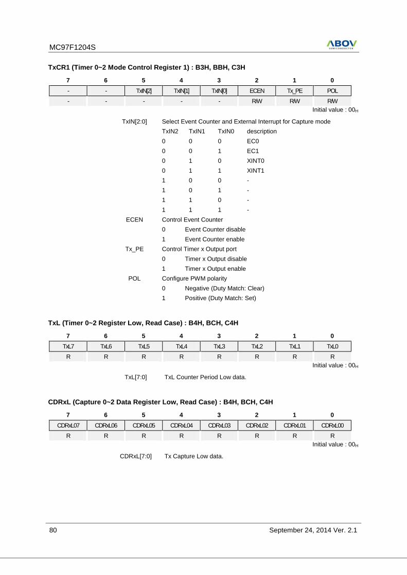
MC97F1204S
80 September 24, 2014 Ver. 2.1
TxCR1 (Timer 0~2 Mode Control Register 1) : B3H, BBH, C3H
7 6 5 4 3 2 1 0
- - TxIN[2] TxIN[1] TxIN[0] ECEN Tx_PE POL
- - - - - R/W R/W R/W
Initial value : 00H
TxIN[2:0] Select Event Counter and External Interrupt for Capture mode
TxIN2 TxIN1 TxIN0 description
0 0 0 EC0
0 0 1 EC1
0 1 0 XINT0
0 1 1 XINT1
1 0 0 -
1 0 1 -
1 1 0 -
1 1 1 -
ECEN Control Event Counter
0 Event Counter disable
1 Event Counter enable
Tx_PE Control Timer x Output port
0 Timer x Output disable
1 Timer x Output enable
POL Configure PWM polarity
0 Negative (Duty Match: Clear)
1 Positive (Duty Match: Set)
TxL (Timer 0~2 Register Low, Read Case) : B4H, BCH, C4H
7 6 5 4 3 2 1 0
TxL7 TxL6 TxL5 TxL4 TxL3 TxL2 TxL1 TxL0
R R R R R R R R
Initial value : 00H
TxL[7:0] TxL Counter Period Low data.
CDRxL (Capture 0~2 Data Register Low, Read Case) : B4H, BCH, C4H
7 6 5 4 3 2 1 0
CDRxL07 CDRxL06 CDRxL05 CDRxL04 CDRxL03 CDRxL02 CDRxL01 CDRxL00
R R R R R R R R
Initial value : 00H
CDRxL[7:0] Tx Capture Low data.
MC97F1204S
September 24, 2014 Ver. 2.1 81
PWMxDRL (PWM 0~2 Duty Register Low, Write Case) : B4H, BCH, C4H
7 6 5 4 3 2 1 0
PWMxDRL7 PWMxDRL6 PWMxDRL5 PWMxDRL4 PWMxDRL3 PWMxDRL2 PWMxDRL1 PWMxDRL0
W W W W W W W W
Initial value : 00H
PWMxDRL[7:0] Tx PWM Duty Low data
Note) Writing is effective only when PWMxE = 1 and TxST = 0
TxH (Timer 0~2 Register High, Read Case) : B5H, BDH, C5H
7 6 5 4 3 2 1 0
TxH7 TxH6 TxH5 TxH4 TxH3 TxH2 TxH1 TxH0
R R R R R R R R
Initial value : 00H
TxH[7:0] TxH Counter Period High data.
CDRxH (Capture 0~2 Data High Register, Read Case) : B5H, BDH, C5H
7 6 5 4 3 2 1 0
CDRxH07 CDRxH06 CDRxH05 CDRxH04 CDRxH03 CDRxH02 CDRxH01 CDRxH00
R R R R R R R R
Initial value : 00H
CDRxH[7:0] Tx Capture High data
PWMxDRH (PWM0~2 Duty Register High, Write Case) : B5H, BDH, C5H
7 6 5 4 3 2 1 0
PWMxDRH7 PWMxDRH6 PWMxDRH5 PWMxDRH4 PWMxDRH3 PWMxDRH2 PWMxDRH1 PWMxDRH0
W W W W W W W W
Initial value : 00H
PWMxDRH[7:0] Tx PWM Duty High data
Note) Writing is effective only when PWMxE = 1 and TxST = 0
TxDRL (Timer 0~2 Data Register Low, Write Case) : B6H, BEH, C6H
7 6 5 4 3 2 1 0
TxDRL7 TxDRL6 TxDRL5 TxDRL4 TxDRL3 TxDRL2 TxDRL1 TxDRL0
W W W W W W W W
Initial value : FFH
TxDRL[7:0] TxL Compare Low data
Note)Be sure to clear PWMxE before loading this register.
MC97F1204S
82 September 24, 2014 Ver. 2.1
PWMxPRL (PWM 0~2 Period Register Low, Write Case) : B6H, BEH, C6H
7 6 5 4 3 2 1 0
PWMxPRL7 PWMxPRL6 PWMxPRL5 PWMxPRL4 PWMxPRL3 PWMxPRL2 PWMxPRL1 PWMxPRL0
W W W W W W W W
Initial value : FFH
PWMxPRL[7:0] TxPWM Period Low data
Note) Writing is effective only when PWMxE = 1 and TxST = 0
TxDRH (Timer 0~2 Data Register High, Write Case) : B7H, BFH, C7H
7 6 5 4 3 2 1 0
TxDRH7 TxDRH6 TxDRH5 TxDRH4 TxDRH3 TxDRH2 TxDRH1 TxDRH0
W W W W W W W W
Initial value : FFH
TxDRH[7:0] TxH Compare High data
Note)Be sure to clear PWMxE before loading this register.
PWMxPRH (PWM 0~2 Period Register High, Write Case) : B7H, BFH, C7H
7 6 5 4 3 2 1 0
PWMxPRH7 PWMxPRH6 PWMxPRH5 PWMxPRH4 PWMxPRH3 PWMxPRH2 PWMxPRH1 PWMxPRH0
R / W W W W W W W W
Initial value : FFH
PWMxPRH[7:0] TxPWM Period High data
Note) Writing is effective only when PWMxE = 1 and TxST = 0
11.4.7 Timer Interrupt Status Register (TMISR)
11.4.7.1 Register description for TMISR
TMISR (Timer Interrupt Status Register) : D5H
7 6 5 4 3 2 1 0
- - - - - TMIF2 TMIF1 TMIF0
- - - - - R R R
Initial value :0H
TMIFx Timer x Interrupt Flag
0 No Timer x interrupt
1 Timer x interrupt occurred, write “1” to clear interrupt flag
Note) The Timer Interrupt Status Register contains interrupt information of each timers. Even if user disabled timer interrupt at IE2, user could check timer interrupt condition from this register.
MC97F1204S
September 24, 2014 Ver. 2.1 83
11.5 SPI
11.5.1 Overview
There is Serial Peripheral Interface (SPI) one channel in MC97F1204S. The SPI allows synchronous
serial data transfer between the external serial devices. It can do Full-duplex communication by 4-wire
(MOSI, MISO, SCK, SS), support Master/Slave mode, can select serial clock (SCK) polarity, phase
and whether LSB first data transfer or MSB first data transfer.
11.5.2 Block Diagram
÷64
÷32
P r e s c a l e r
MUX
÷2
÷4
÷8
÷16 fSCLK
PxDA[x]
SPICR[2:0]
3
MUX Edge
Detector
SPI Control
Circuit
WCOL
TCIR
SCK SCK
Control
MS
MS
MISO
MUX
MS
MOSI
8bit Shift
Register
SPIDR (8Bit)
DEP
SS SS
Control
MS
PxIO[x]
SPIEN
FLSB
SPI Interrupt
CPOL CPHA
Internal Bus Line
8
SPIEN FLSB MS CPOL CPHA DSCR SCR1 SCR0 SPICR ADDRESS :D2H
INITIAL VALUE : 0000_0000B
TCIR WCOL SS_HIGH - TWOPIN SSENA TXENA RXENA SPISR ADDRESS :D4H
INITIAL VALUE : 00--_-000B
÷128
FLSB
INT_ACK
Clear
MUX
MUX
TWOPIN
(MISO)
(MOSI)
0
1
0
1
0
0
1
1
Figure 11-10 SPI Block Diagram
MC97F1204S
84 September 24, 2014 Ver. 2.1
11.5.3 Data Transmit / Receive Operation
User can use SPI for serial data communication by following step
1. Select SPI operation mode(master/slave, polarity, phase) by control register SPICR.
2. When the SPI is configured as a Master, it selects a Slave by SS signal (active low).
When the SPI is configured as a Slave, it is selected by SS signal incoming from Master
3. When the user writes a byte to the data register SPIDR, SPI will start an operation.
4. In this time, if the SPI is configured as a Master, serial clock will come out of SCK pin. And Master
shifts the eight bits into the Slave (transmit), Slave shifts the eight bits into the Master at the same
time (receive). If the SPI is configured as a Slave, serial clock will come into SCK pin. And Slave
shifts the eight bits into the Master (transmit), Master shifts the eight bits into the Slave at the same
time (receive).
5. When transmit/receive is done, TCIR (Transmit Complete or Interrupt Request) bit will be set. If the
SPI interrupt is enabled, an interrupt is requested. And TCIR bit is cleared by hardware when
executing the corresponding interrupt. If SPI interrupt is disable, TCIR bit is cleared when user read
the status register SPISR, and then access (read/write) the data register SPIDR.
Note) If you want to use both transmit and receive, set the TXENA, RXENA bit of SPISR, and if user
want to use only either transmit or receive, clear the TXENA or RXENA. In this case, user can use
disabled pin by GPIO freely.
11.5.4 SS pin function
1. When the SPI is configured as a Slave, the SS pin is always input. If LOW signal come into SS pin, the SPI logic is active. And if HIGH signal come into SS pin, the SPI logic is stop. In this time, SPI logic will be reset, and invalidate any transmitted or received data.
2. When the SPI is configured as a Master, the user can select the direction of the SS pin by port direction register (PxIO[x]). If the SS pin is configured as an output, user can use general GPIO output mode. If the SS pin is configured as an input, ‘HIGH’ signal must come into SS pin to guarantee Master operation. If ‘LOW’ signal come into SS pin, the SPI logic interprets this as another master selecting the SPI as a slave and starting to send data to it. To avoid bus contention, MS bit of SPICR will be cleared and the SPI becomes a Slave and then, TCIR bit of SPISR will be set, and if the SPI interrupt is enabled, an interrupt is requested.
Note)
- When the SS pin is configured as an output at Master mode, SS pin’s output value is defined by
user’s software (PxDA[x]). Before SPICR setting, the direction of SS pin must be defined
- If you don’t need to use SS pin, clear the SSENA bit of SPISR. So, you can use disabled pin by
GPIO freely. In this case, SS signal is driven by ‘HIGH’ or ‘LOW’ internally. (master is ‘HIGH’, salve
is ‘LOW’)
- When SS pin is configured as input(master or slave), if ‘HIGH’ signal come into SS pin, this flag
bit(SS_HIGH) will be set at the SS rising time. And you can clear it by writing ‘0’.
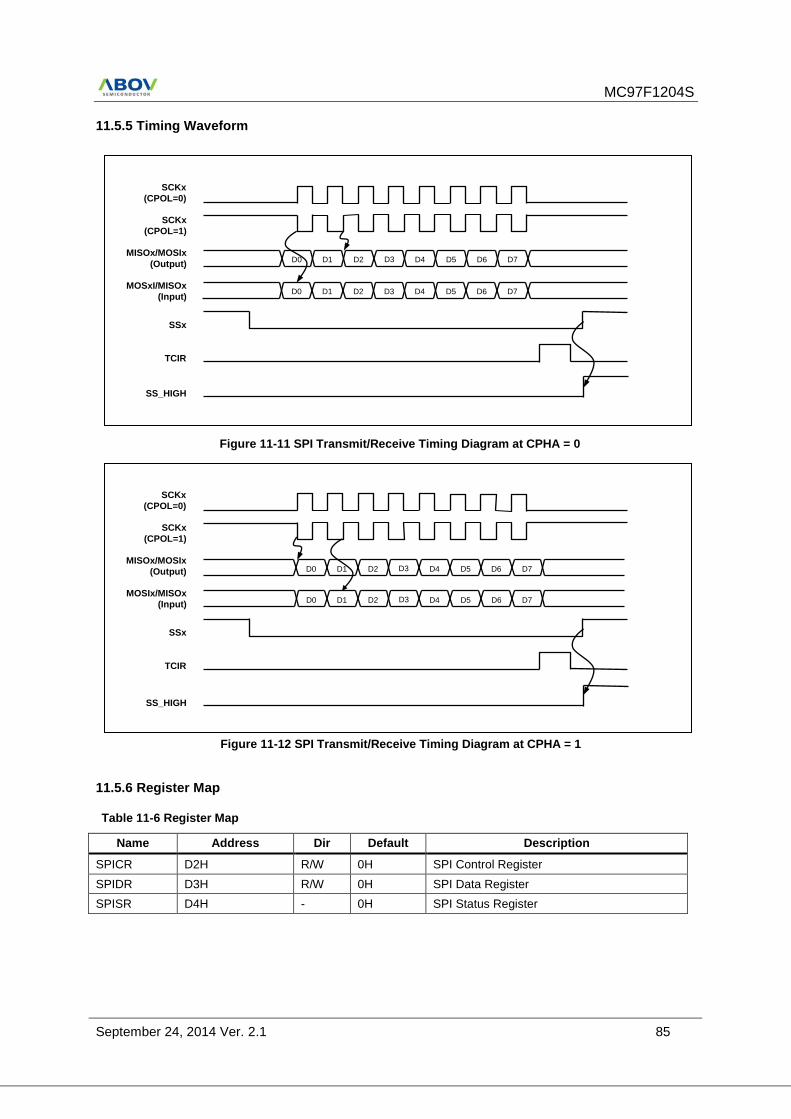
MC97F1204S
September 24, 2014 Ver. 2.1 85
11.5.5 Timing Waveform
11.5.6 Register Map
Table 11-6 Register Map
Name Address Dir Default Description
SPICR D2H R/W 0H SPI Control Register
SPIDR D3H R/W 0H SPI Data Register
SPISR D4H - 0H SPI Status Register
SCKx
(CPOL=0)
SCKx
(CPOL=1)
SSx
TCIR
MISOx/MOSIx
(Output) D0 D1 D2 D3 D4 D5 D6 D7
MOSxI/MISOx
(Input) D0 D1 D2 D3 D4 D5 D6 D7
SS_HIGH
SCKx
(CPOL=0)
SCKx
(CPOL=1)
MISOx/MOSIx
(Output)
MOSIx/MISOx
(Input)
SSx
TCIR
D0 D1 D2 D3 D4 D5 D6 D7
D0 D1 D2 D3 D4 D5 D6 D7
SS_HIGH
Figure 11-11 SPI Transmit/Receive Timing Diagram at CPHA = 0
Figure 11-12 SPI Transmit/Receive Timing Diagram at CPHA = 1
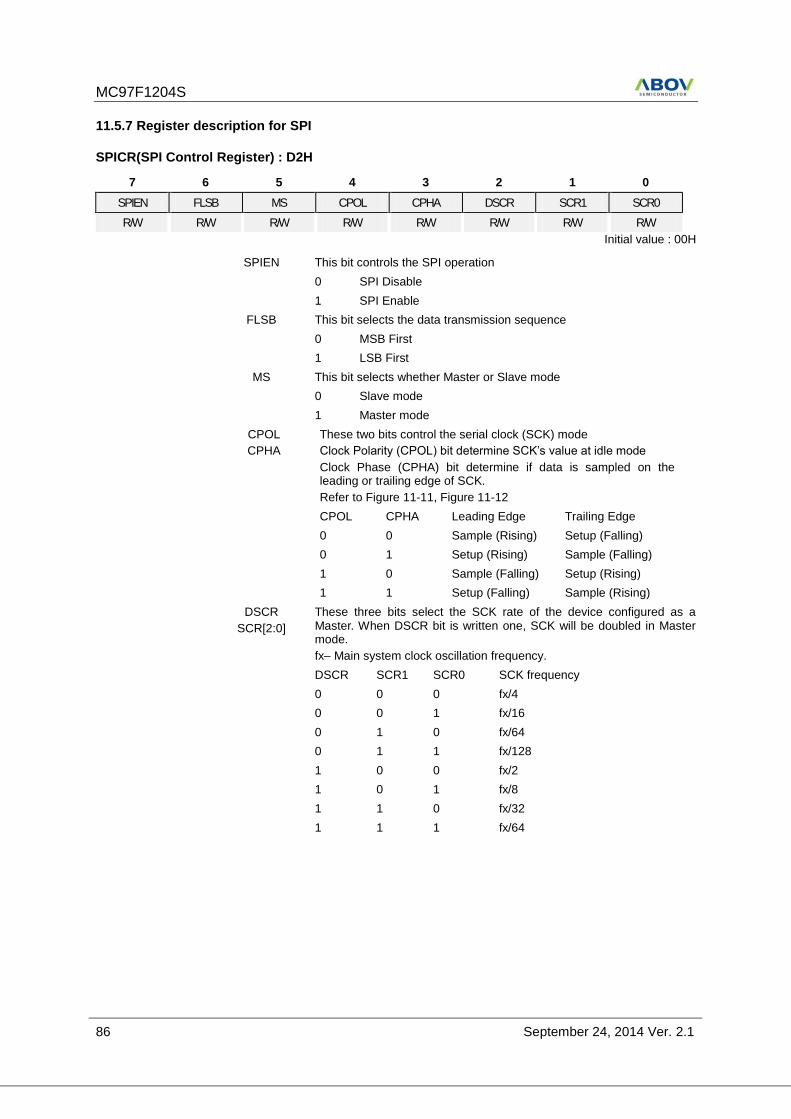
MC97F1204S
86 September 24, 2014 Ver. 2.1
11.5.7 Register description for SPI
SPICR(SPI Control Register) : D2H
7 6 5 4 3 2 1 0
SPIEN FLSB MS CPOL CPHA DSCR SCR1 SCR0
R/W R/W R/W R/W R/W R/W R/W R/W
Initial value : 00H
SPIEN This bit controls the SPI operation
0 SPI Disable
1 SPI Enable
FLSB This bit selects the data transmission sequence
0 MSB First
1 LSB First
MS This bit selects whether Master or Slave mode
0 Slave mode
1 Master mode
CPOL
CPHA
These two bits control the serial clock (SCK) mode
Clock Polarity (CPOL) bit determine SCK’s value at idle mode
Clock Phase (CPHA) bit determine if data is sampled on the leading or trailing edge of SCK.
Refer to Figure 11-11, Figure 11-12
CPOL CPHA Leading Edge Trailing Edge
0 0 Sample (Rising) Setup (Falling)
0 1 Setup (Rising) Sample (Falling)
1 0 Sample (Falling) Setup (Rising)
1 1 Setup (Falling) Sample (Rising)
DSCR
SCR[2:0]
These three bits select the SCK rate of the device configured as a Master. When DSCR bit is written one, SCK will be doubled in Master mode.
fx– Main system clock oscillation frequency.
DSCR SCR1 SCR0 SCK frequency
0 0 0 fx/4
0 0 1 fx/16
0 1 0 fx/64
0 1 1 fx/128
1 0 0 fx/2
1 0 1 fx/8
1 1 0 fx/32
1 1 1 fx/64
MC97F1204S
September 24, 2014 Ver. 2.1 87
SPIDR(SPI Data Register) : D3H
7 6 5 4 3 2 1 0
SPIDR7 SPIDR6 SPIDR5 SPIDR4 SPIDR3 SPIDR2 SPIDR1 SPIDR0
R/W R/W R/W R/W R/W R/W R/W R/W
Initial value : 00H
SPIDR [7:0] SPI data register.
Although you only use reception, user must write any data in here to start the SPI operation.
SPISR (SPI Status Register) : D4H
7 6 5 4 3 2 1 0
TCIR WCOL SS_HIGH - TWOPIN SSENA TXENA RXENA
R R R/W - R/W R/W R/W R/W
Initial value : 00H
TCIR When a serial data transmission is complete, the TCIR bit is set. If the SPI interrupt is enabled, an interrupt is requested. And TCIR bit is cleared by hardware when executing the corresponding interrupt. If SPI interrupt is disable, TCIR bit is cleared when user read the status register SPISR, and then access (read/write) the data register SPIDR.
0 Interrupt cleared
1 Transmission Complete and Interrupt Requested
WCOL This bit is set if the data register SPIDR is written during a data transfer. This bit is cleared when user read the status register SPISR, and then access (read/write) the data register SPIDR.
0 No collision
1 Write Collision
SS_HIGH When SS pin is configured as input(master or slave), if ‘HIGH’ signal come into SS pin, this flag bit will be set at the SS rising time. And you can clear it by writing ‘0’.
You can write only zero.
0 Flag is cleared
1 Flag is set
TWOPIN This bit controls the 2 pin operation.
In master mode,
0 Disable
1 Enable
SSENA This bit controls the SS pin operation
0 Disable
1 Enable
TXENA This bit controls a data transfer operation
0 Disable
1 Enable
RXENA This bit controls a data reception operation
0 Disable
1 Enable
Note that if TWOPIN is set to '1', MOSI and MISO pins are changed.
MC97F1204S
88 September 24, 2014 Ver. 2.1
11.6 12-Bit A/D Converter
11.6.1 Overview
The analog-to-digital converter (A/D) allows conversion of an analog input signal to a corresponding
12-bit digital value. The A/D module has fifteenth analog inputs. The output of the multiplex is the
input into the converter, which generates the result via successive approximation. The A/D module
has four registers which are the control register ADCM (A/D Converter Mode Register), ADCM1 (A/D
Converter Mode Register 1) and A/D result register ADCHR (A/D Converter Result High Register) and
ADCLR (A/D Converter Result Low Register). It is selected for the corresponding channel to be
converted by setting ADSEL[3:0]. To executing A/D conversion, ADST bit sets to ‘1’. The register
ADCHR and ADCLR contains the results of the A/D conversion. When the conversion is completed,
the result is loaded into the ADCHR and ADCLR, the A/D conversion status bit AFLAG is set to ‘1’,
and the A/D interrupt is set. While processing A/D conversion, AFLAG bit is read as ‘0’. If using STBY
(power down) bit, the ADC is disabled. Also interrupt of internal timer, external event can start ADC
regardless of interrupt occurrence.
ADC Conversion Time = ADCLK * 60 cycles
After STBY bit is reset (ADC power enable) and it is restarted, during some cycle, ADC conversion
value may have an inaccurate value.
When using ports as ADC input port, it is recommended to set corresponding PSR2, PSR3 register
to prevent current leakage or unexpected function, because analog value enters to digital circuit.
ADC zero offset value is written to 4007h of option memory.
To read the zero offset value, refer to the assembly code below.
(Example)
char Zero_offset; // signed value
#pragma ASM
mov A, #0 ;
mov DPTR, #4007h ; ADC Zero offset value is addressed at 0x4007
mov A, @A+DPTR ; A = ADC zero offset value
#pragma ENDASM
Zero_offset = ACC; //
Note) When using the ADC, set the direction of the port as input mode. (PxIO)
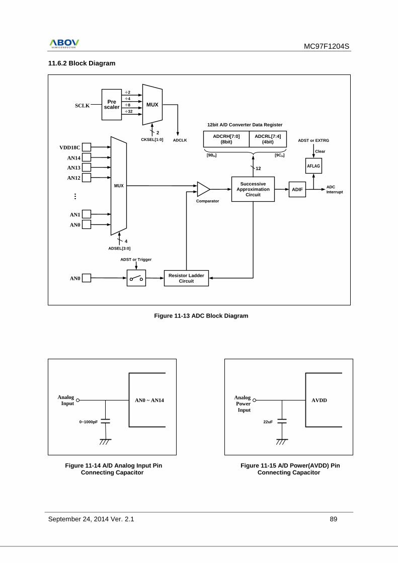
MC97F1204S
September 24, 2014 Ver. 2.1 89
11.6.2 Block Diagram
MUX
VDD18C
AN14
AN13
AN12
AN1
AN0
Successive Approximation
Circuit ADIF
ADCRH[7:0]
(8bit)
ADCRL[7:4]
(4bit)
AFLAG
Resistor Ladder
Circuit
ADST or Trigger
AN0
12bit A/D Converter Data Register
ADSEL[3:0]
4
12
ADC
Interrupt
Pre scaler MUX
÷2
÷4
÷8
÷32
SCLK
CKSEL[1:0]
2
ADST or EXTRG
Clear
Comparator
[9BH] [9CH]
ADCLK
0~1000pF
AN0 ~ AN14 Analog
Input
22uF
AVDD Analog
Power
Input
Figure 11-14 A/D Analog Input Pin Connecting Capacitor
Figure 11-15 A/D Power(AVDD) Pin Connecting Capacitor
Figure 11-13 ADC Block Diagram
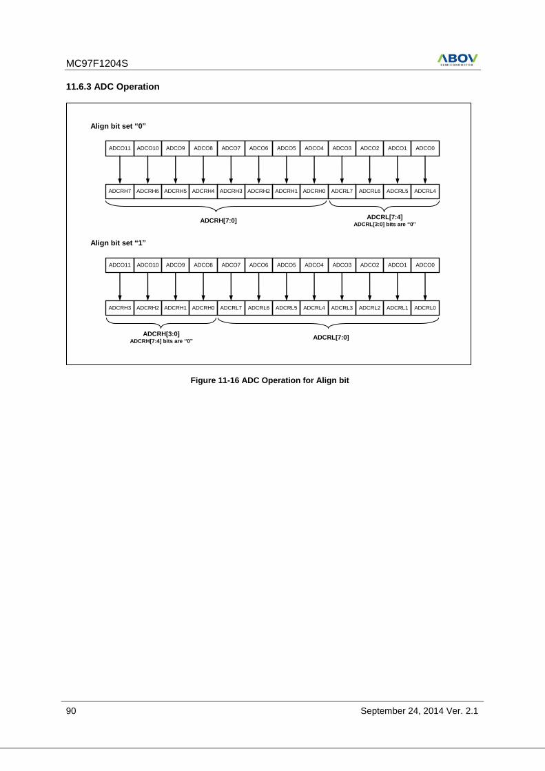
MC97F1204S
90 September 24, 2014 Ver. 2.1
11.6.3 ADC Operation
Align bit set “0”
ADCO11 ADCO10 ADCO9 ADCO8 ADCO7 ADCO6 ADCO5 ADCO4 ADCO3 ADCO2 ADCO1 ADCO0
ADCRH7 ADCRH6 ADCRH5 ADCRH4 ADCRH3 ADCRH2 ADCRH1 ADCRH0 ADCRL7 ADCRL6 ADCRL5 ADCRL4
ADCRH[7:0] ADCRL[7:4]
ADCRL[3:0] bits are “0”
Align bit set “1”
ADCO11 ADCO10 ADCO9 ADCO8 ADCO7 ADCO6 ADCO5 ADCO4 ADCO3 ADCO2 ADCO1 ADCO0
ADCRH3 ADCRH2 ADCRH1 ADCRH0 ADCRL7 ADCRL6 ADCRL5 ADCRL4 ADCRL3 ADCRL2 ADCRL1 ADCRL0
ADCRL[7:0] ADCRH[3:0]
ADCRH[7:4] bits are “0”
Figure 11-16 ADC Operation for Align bit
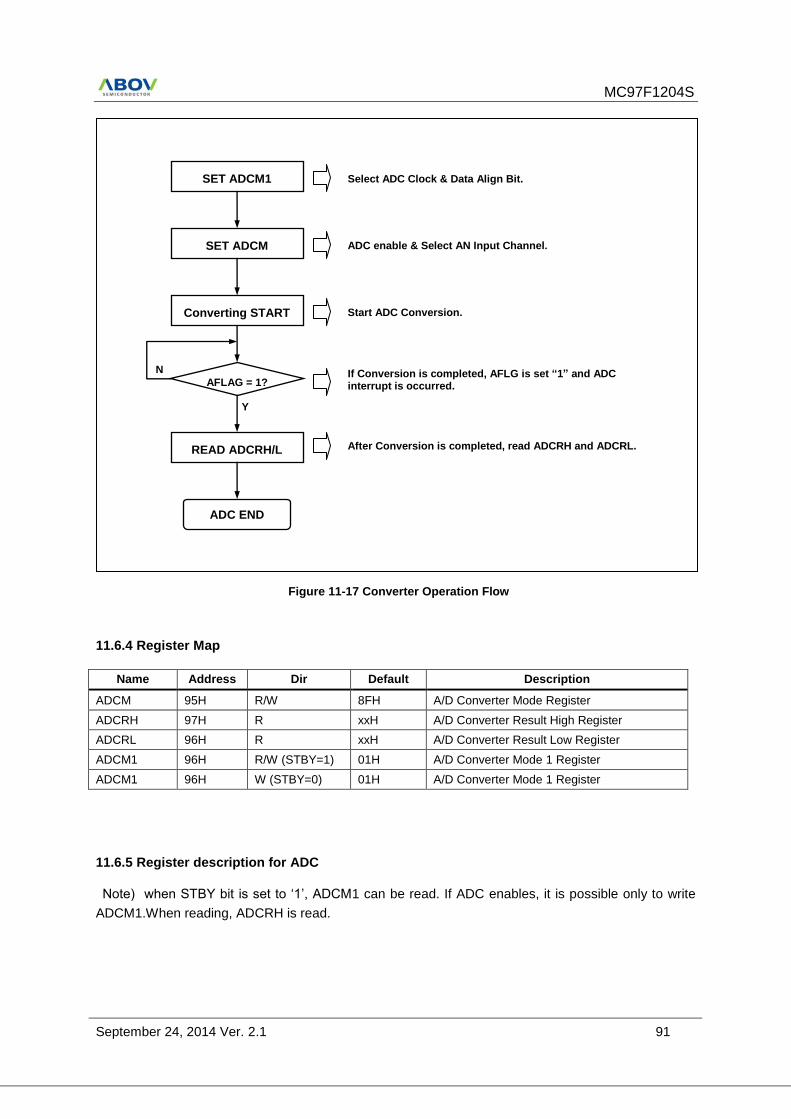
MC97F1204S
September 24, 2014 Ver. 2.1 91
11.6.4 Register Map
Name Address Dir Default Description
ADCM 95H R/W 8FH A/D Converter Mode Register
ADCRH 97H R xxH A/D Converter Result High Register
ADCRL 96H R xxH A/D Converter Result Low Register
ADCM1 96H R/W (STBY=1) 01H A/D Converter Mode 1 Register
ADCM1 96H W (STBY=0) 01H A/D Converter Mode 1 Register
11.6.5 Register description for ADC
Note) when STBY bit is set to ‘1’, ADCM1 can be read. If ADC enables, it is possible only to write
ADCM1.When reading, ADCRH is read.
SET ADCM1
SET ADCM
AFLAG = 1?
Converting START
READ ADCRH/L
ADC END
Select ADC Clock & Data Align Bit.
ADC enable & Select AN Input Channel.
Start ADC Conversion.
If Conversion is completed, AFLG is set “1” and ADC interrupt is occurred.
After Conversion is completed, read ADCRH and ADCRL.
Y
N
Figure 11-17 Converter Operation Flow
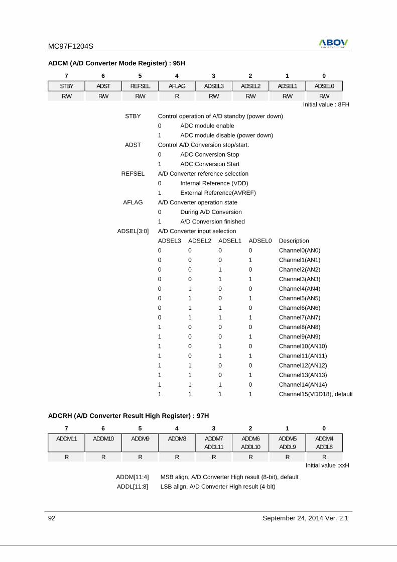
MC97F1204S
92 September 24, 2014 Ver. 2.1
ADCM (A/D Converter Mode Register) : 95H
7 6 5 4 3 2 1 0
STBY ADST REFSEL AFLAG ADSEL3 ADSEL2 ADSEL1 ADSEL0
R/W R/W R/W R R/W R/W R/W R/W
Initial value : 8FH
STBY Control operation of A/D standby (power down)
0 ADC module enable
1 ADC module disable (power down)
ADST Control A/D Conversion stop/start.
0 ADC Conversion Stop
1 ADC Conversion Start
REFSEL A/D Converter reference selection
0 Internal Reference (VDD)
1 External Reference(AVREF)
AFLAG A/D Converter operation state
0 During A/D Conversion
1 A/D Conversion finished
ADSEL[3:0] A/D Converter input selection
ADSEL3 ADSEL2 ADSEL1 ADSEL0 Description
0 0 0 0 Channel0(AN0)
0 0 0 1 Channel1(AN1)
0 0 1 0 Channel2(AN2)
0 0 1 1 Channel3(AN3)
0 1 0 0 Channel4(AN4)
0 1 0 1 Channel5(AN5)
0 1 1 0 Channel6(AN6)
0 1 1 1 Channel7(AN7)
1 0 0 0 Channel8(AN8)
1 0 0 1 Channel9(AN9)
1 0 1 0 Channel10(AN10)
1 0 1 1 Channel11(AN11)
1 1 0 0 Channel12(AN12)
1 1 0 1 Channel13(AN13)
1 1 1 0 Channel14(AN14)
1 1 1 1 Channel15(VDD18), default
ADCRH (A/D Converter Result High Register) : 97H
7 6 5 4 3 2 1 0
ADDM11
ADDM10
ADDM9
ADDM8
ADDM7
ADDL11
ADDM6
ADDL10
ADDM5
ADDL9
ADDM4
ADDL8
R R R R R R R R
Initial value :xxH
ADDM[11:4] MSB align, A/D Converter High result (8-bit), default
ADDL[11:8] LSB align, A/D Converter High result (4-bit)
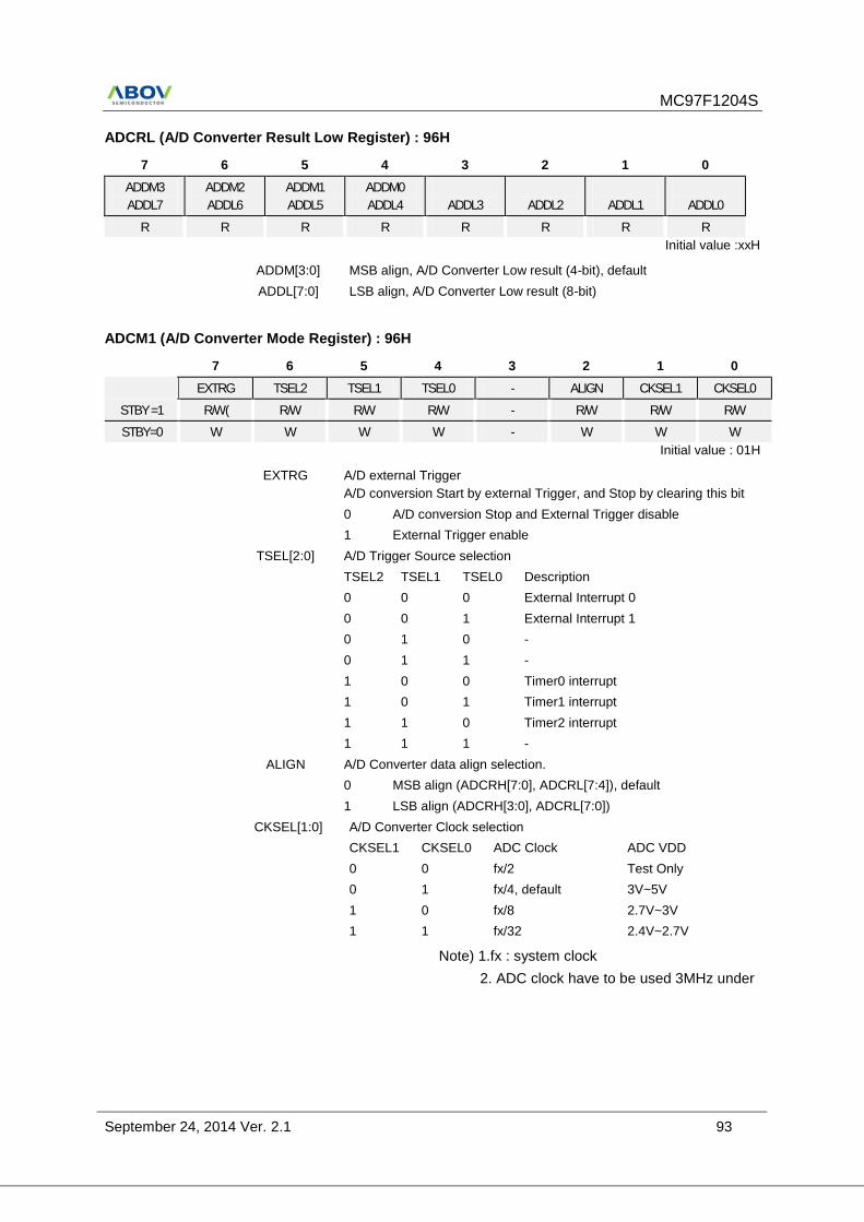
MC97F1204S
September 24, 2014 Ver. 2.1 93
ADCRL (A/D Converter Result Low Register) : 96H
7 6 5 4 3 2 1 0
ADDM3
ADDL7
ADDM2
ADDL6
ADDM1
ADDL5
ADDM0
ADDL4
ADDL3
ADDL2
ADDL1
ADDL0
R R R R R R R R
Initial value :xxH
ADDM[3:0] MSB align, A/D Converter Low result (4-bit), default
ADDL[7:0] LSB align, A/D Converter Low result (8-bit)
ADCM1 (A/D Converter Mode Register) : 96H
7 6 5 4 3 2 1 0
EXTRG TSEL2 TSEL1 TSEL0 - ALIGN CKSEL1 CKSEL0
STBY =1 R/W( R/W R/W R/W - R/W R/W R/W
STBY=0 W W W W - W W W
Initial value : 01H
EXTRG A/D external Trigger
A/D conversion Start by external Trigger, and Stop by clearing this bit
0 A/D conversion Stop and External Trigger disable
1 External Trigger enable
TSEL[2:0] A/D Trigger Source selection
TSEL2 TSEL1 TSEL0 Description
0 0 0 External Interrupt 0
0 0 1 External Interrupt 1
0 1 0 -
0 1 1 -
1 0 0 Timer0 interrupt
1 0 1 Timer1 interrupt
1 1 0 Timer2 interrupt
1 1 1 -
ALIGN A/D Converter data align selection.
0 MSB align (ADCRH[7:0], ADCRL[7:4]), default
1 LSB align (ADCRH[3:0], ADCRL[7:0])
CKSEL[1:0] A/D Converter Clock selection
CKSEL1 CKSEL0 ADC Clock ADC VDD
0 0 fx/2 Test Only
0 1 fx/4, default 3V~5V
1 0 fx/8 2.7V~3V
1 1 fx/32 2.4V~2.7V
Note) 1.fx : system clock
2. ADC clock have to be used 3MHz under
MC97F1204S
94 September 24, 2014 Ver. 2.1
12. Power Down Operation
12.1 Overview
The MC97F1204S has three power-down modes to minimize the power consumption of the device.
In power down mode, power consumption is reduced considerably. The device provides three kinds of
power saving functions, IDLE, STOP1 and STOP2 mode. In three modes, program is stopped.
To go to STOP1 mode, WDTRC should be set by writing '1' to WDTRCON bit in SCCR register.
12.2 Peripheral Operation in IDLE/STOP Mode
Table 12-1 Peripheral Operation during Power Down Mode.
Peripheral IDLE Mode STOP1 Mode STOP2 Mode
CPU ALL CPU Operation are Disable
ALL CPU Operation are Disable ALL CPU Operation are Disable
RAM Retain Retain Retain
Basic Interval Timer
Operates Continuously
Operates Continuously Stop
Watch Dog Timer
Operates Continuously
Operates Continuously Stop
Timer Operates Continuously
Halted (Only when the Event Counter Mode is Enable, Timer operates Normally)
Halted (Only when the Event Counter Mode is Enable, Timer operates Normally)
SPI Operates Continuously
Only operate with external clock Only operate with external clock
Internal OSC
(8MHz)
Oscillation Stop Stop
Internal RCOSC (64kHz)
Oscillation Oscillation Stop
I/O Port Retain Retain Retain
Control Register
Retain Retain Retain
Address Data Bus
Retain Retain Retain
Release Method
By RESET, all Interrupts
By RESET, SPI (External clock), External Interrupt (with PCI),WDT, BIT, BOD, TIMER(EC)
By RESET, SPI (External clock), External Interrupt (with PCI), BODTIMER(EC)
MC97F1204S
September 24, 2014 Ver. 2.1 95
12.3 IDLE mode
The power control register is set to ‘01h’ to enter the IDLE Mode. In this mode, the internal oscillation
circuits remain active. Oscillation continues and peripherals are operated normally but CPU stops. It is
released by reset or interrupt. To be released by interrupt, interrupt should be enabled before IDLE
mode. If using reset, because the device becomes initialized state, the registers have reset value.
(Ex) MOV PCON, #00000001b ; setting of IDLE mode : set the bit of STOP and IDLE Control register (PCON)
External
Interrupt
OSC
Normal Operation
Release
CPU Clock
Stand-by Mode Normal Operation
Figure 12-1 IDLE Mode Release Timing by External Interrupt
Figure 12-2 IDLE Mode Release Timing by /RESET
OSC
CPU Clock
RESETB
Normal Operation
BIT Counter
IDLE Mode Normal Operation
Release Set PCON
to 01
Clear & Start
TST = 65.5ms @ 8MHz
m-2 m-1 m n 0 0 0 1 FD FE FF 0 1
TOSC = 1/fOSC fOSC = 8MHz BCK[1:0] in BCCR = 00B
BPD[2:0] in BCCR = 111B
2048 TOSC
MC97F1204S
96 September 24, 2014 Ver. 2.1
12.4 STOP mode
The power control register is set to ‘03h’ to enter the STOP Mode. In the stop mode, the main
oscillator, system clock and peripheral clock is stopped, but watch timer continue to operate if
WDTRCON bit in SCCR register is written to '1'. With the clock frozen, all functions are stopped, but
the on-chip RAM and control registers are held.
The source for exit from STOP mode is hardware reset and interrupts. The reset re-defines all the
control registers.
When exit from STOP mode, enough oscillation stabilization time is required to normal operation.
Figure 12-3 shows the timing diagram. When released from STOP mode, the Basic interval timer is
activated on wake-up. Therefore, before STOP instruction, user must be set its relevant prescaler
divide ratio to have long enough time (more than 20msec). this guarantees that oscillator has started
and stabilized.
OSC
CPU Clock
RESETB
Normal Operation
BIT Counter
STOP Mode Normal Operation
Release STOP Command
Clear & Start
TST = 65.5ms @ 8MHz
m-2 m-1 m n FF 0 1 1 2 FE
TOSC = 1/fOSC BPD[2:0] in BCCR = 111B
0
2048 TOSC
OSC
CPU Clock
External
Interrupt
Normal Operation
BIT Counter
STOP Mode Normal Operation
Release
STOP Command
Clear & Start
TST > 20ms by Software
Before executing STOP command, BCCR must be set properly by software to get stability time is to be longer than 20ms.
n n+1 n+2 n+3 FF 0 1 1 2 FE
TOSC = 1/fOSC
BPD[2:0] in BCCR = 111B
0
2048 TOSC
Figure 12-3 STOP Mode Release Timing by External Interrupt
Figure 12-4 STOP Mode Release Timing by /RESET
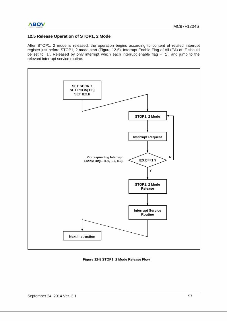
MC97F1204S
September 24, 2014 Ver. 2.1 97
12.5 Release Operation of STOP1, 2 Mode
After STOP1, 2 mode is released, the operation begins according to content of related interrupt register just before STOP1, 2 mode start (Figure 12-5). Interrupt Enable Flag of All (EA) of IE should be set to `1`. Released by only interrupt which each interrupt enable flag = `1`, and jump to the relevant interrupt service routine.
SET SCCR.7 SET PCON[1:0]
SET IEx.b
STOP1, 2 Mode
IEX.b==1 ?
Interrupt Request
STOP1, 2 Mode Release
Y
Interrupt Service Routine
Next Instruction
N Corresponding Interrupt
Enable Bit(IE, IE1, IE2, IE3)
Figure 12-5 STOP1, 2 Mode Release Flow
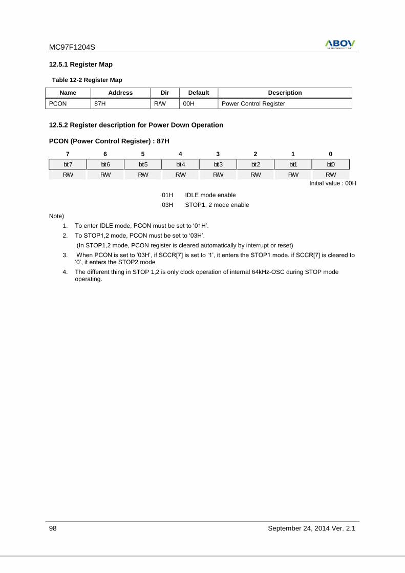
MC97F1204S
98 September 24, 2014 Ver. 2.1
12.5.1 Register Map
Table 12-2 Register Map
Name Address Dir Default Description
PCON 87H R/W 00H Power Control Register
12.5.2 Register description for Power Down Operation
PCON (Power Control Register) : 87H
7 6 5 4 3 2 1 0
bit 7 bit 6 bit 5 bit 4 bit 3 bit 2 bit1 bit0
R/W R/W R/W R/W R/W R/W R/W R/W
Initial value : 00H
01H IDLE mode enable
03H STOP1, 2 mode enable
Note)
1. To enter IDLE mode, PCON must be set to ‘01H’.
2. To STOP1,2 mode, PCON must be set to ‘03H’.
(In STOP1,2 mode, PCON register is cleared automatically by interrupt or reset)
3. When PCON is set to ‘03H’, if SCCR[7] is set to ‘1’, it enters the STOP1 mode. if SCCR[7] is cleared to ‘0’, it enters the STOP2 mode
4. The different thing in STOP 1,2 is only clock operation of internal 64kHz-OSC during STOP mode operating.
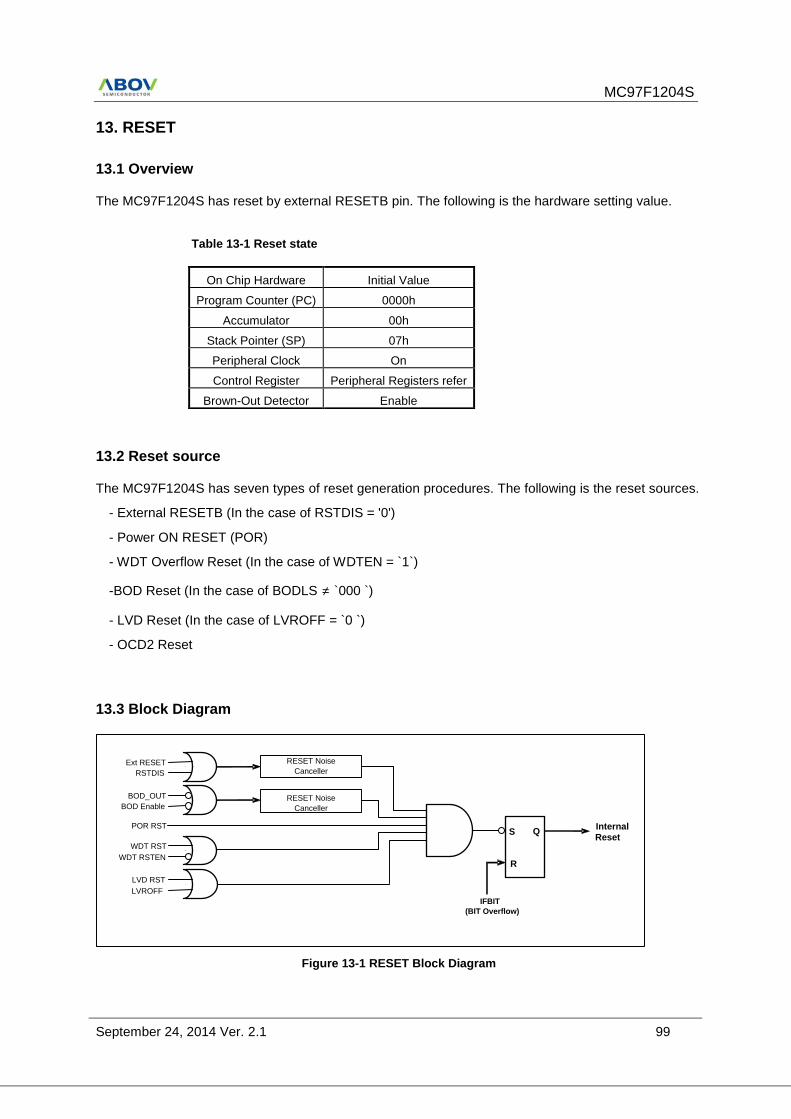
MC97F1204S
September 24, 2014 Ver. 2.1 99
13. RESET
13.1 Overview
The MC97F1204S has reset by external RESETB pin. The following is the hardware setting value.
Table 13-1 Reset state
13.2 Reset source
The MC97F1204S has seven types of reset generation procedures. The following is the reset sources.
- External RESETB (In the case of RSTDIS = '0')
- Power ON RESET (POR)
- WDT Overflow Reset (In the case of WDTEN = `1`)
-BOD Reset (In the case of BODLS ≠ `000 `)
- LVD Reset (In the case of LVROFF = `0 `)
- OCD2 Reset
13.3 Block Diagram
WDT RST
WDT RSTEN
Ext RESET
RSTDIS
RESET Noise
Canceller
BOD_OUT
BOD Enable RESET Noise
Canceller
POR RST S Q
R
Internal Reset
IFBIT
(BIT Overflow)
LVD RST
LVROFF
Figure 13-1 RESET Block Diagram
On Chip Hardware Initial Value
Program Counter (PC) 0000h
Accumulator 00h
Stack Pointer (SP) 07h
Peripheral Clock On
Control Register Peripheral Registers refer
Brown-Out Detector Enable
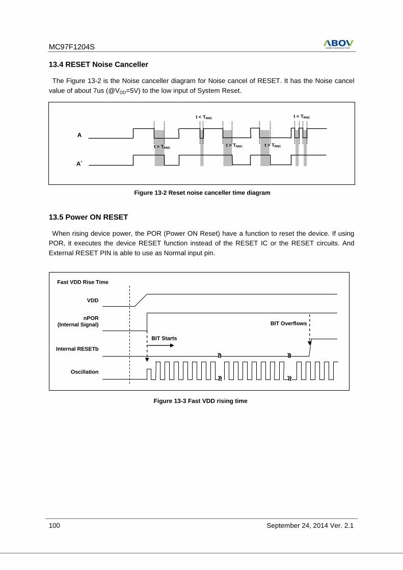
MC97F1204S
100 September 24, 2014 Ver. 2.1
13.4 RESET Noise Canceller
The Figure 13-2 is the Noise canceller diagram for Noise cancel of RESET. It has the Noise cancel
value of about 7us (@VDD=5V) to the low input of System Reset.
13.5 Power ON RESET
When rising device power, the POR (Power ON Reset) have a function to reset the device. If using
POR, it executes the device RESET function instead of the RESET IC or the RESET circuits. And
External RESET PIN is able to use as Normal input pin.
VDD
nPOR
(Internal Signal)
Internal RESETb
Oscillation
BIT Starts
BIT Overflows
Fast VDD Rise Time
t > TRNC t > TRNC t > TRNC
t < TRNC t < TRNC
A
A’
Figure 13-2 Reset noise canceller time diagram
Figure 13-3 Fast VDD rising time
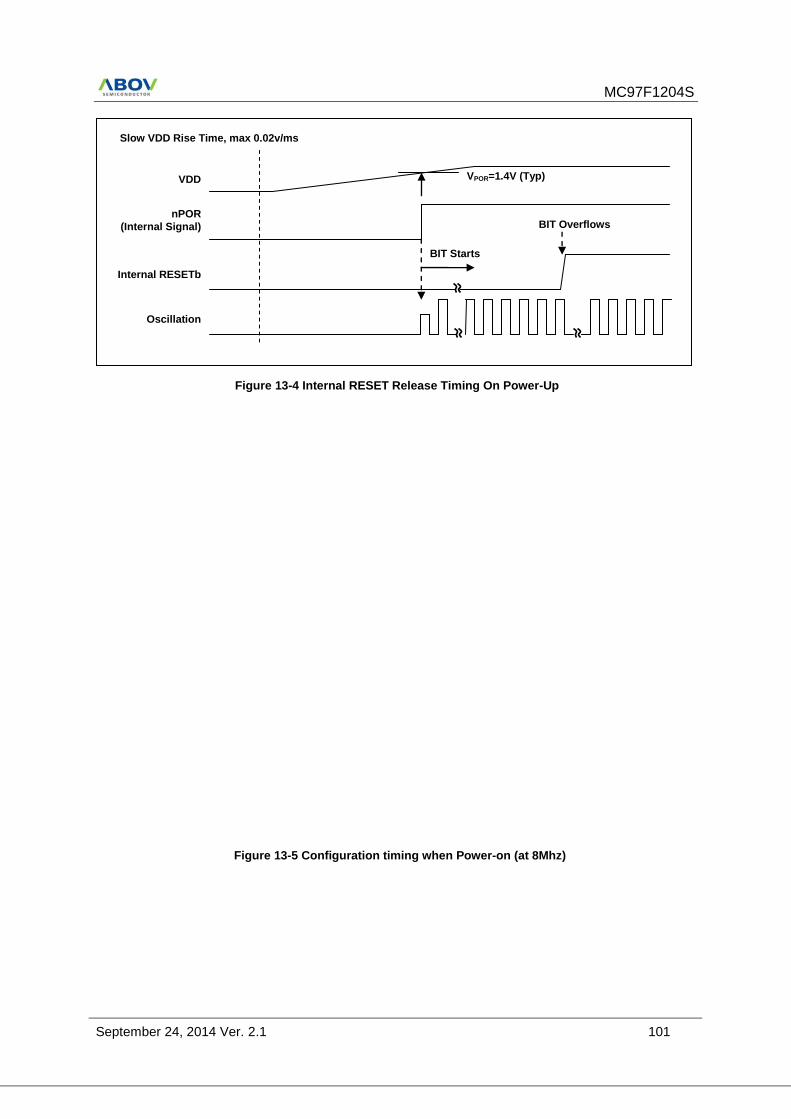
MC97F1204S
September 24, 2014 Ver. 2.1 101
VDD
nPOR
(Internal Signal)
Internal RESETb
Oscillation
BIT Starts
BIT Overflows
Slow VDD Rise Time, max 0.02v/ms
VPOR=1.4V (Typ)
Figure 13-4 Internal RESET Release Timing On Power-Up
Figure 13-5 Configuration timing when Power-on (at 8Mhz)
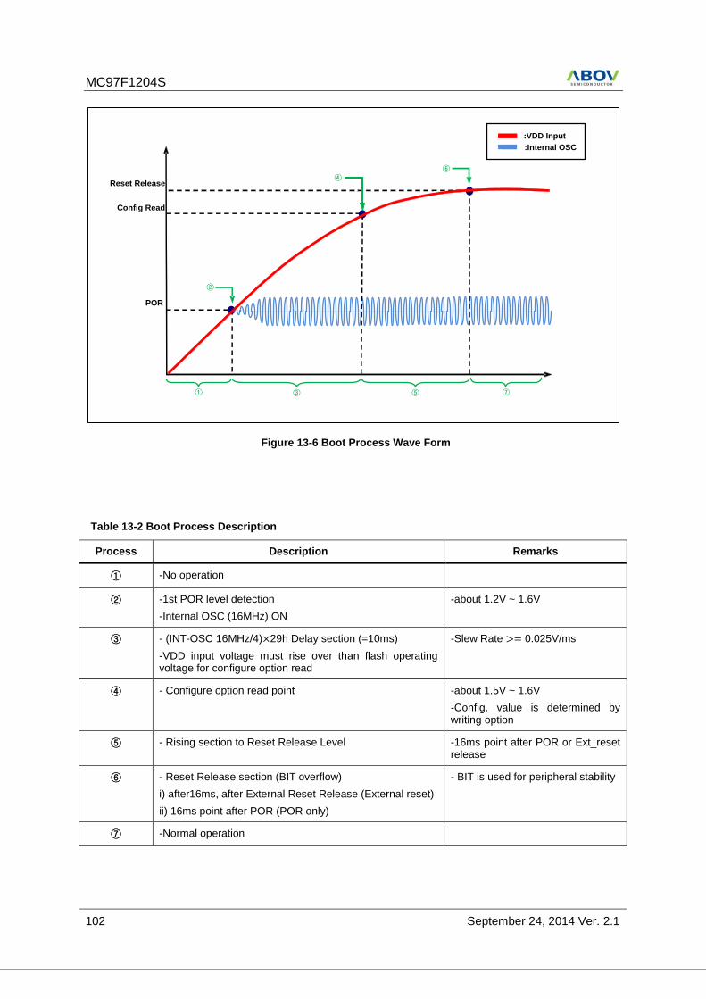
MC97F1204S
102 September 24, 2014 Ver. 2.1
Reset Release
Config Read
POR
:VDD Input
:Internal OSC
①
②
③
④
⑤
⑥
⑦
Table 13-2 Boot Process Description
Process Description Remarks
① -No operation
② -1st POR level detection
-Internal OSC (16MHz) ON
-about 1.2V ~ 1.6V
③ - (INT-OSC 16MHz/4) 29h Delay section (=10ms)
-VDD input voltage must rise over than flash operating voltage for configure option read
-Slew Rate 0.025V/ms
④ - Configure option read point -about 1.5V ~ 1.6V
-Config. value is determined by writing option
⑤ - Rising section to Reset Release Level -16ms point after POR or Ext_reset release
⑥ - Reset Release section (BIT overflow)
i) after16ms, after External Reset Release (External reset)
ii) 16ms point after POR (POR only)
- BIT is used for peripheral stability
⑦ -Normal operation
Figure 13-6 Boot Process Wave Form
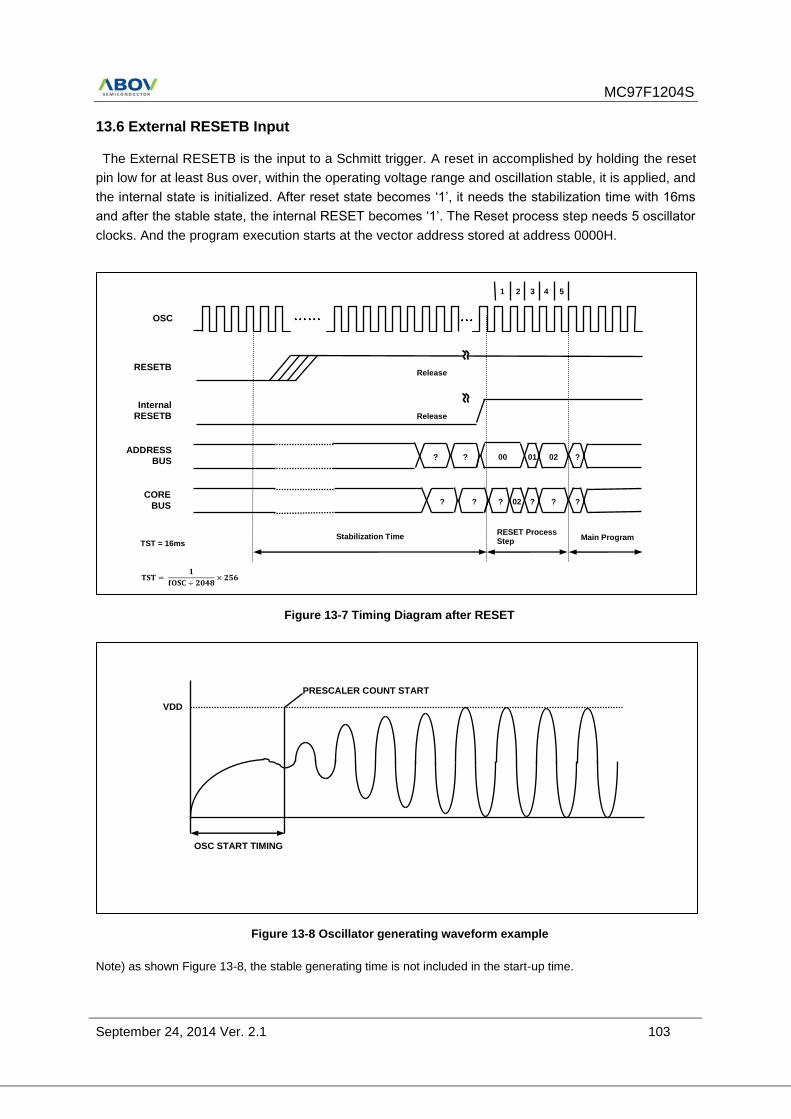
MC97F1204S
September 24, 2014 Ver. 2.1 103
13.6 External RESETB Input
The External RESETB is the input to a Schmitt trigger. A reset in accomplished by holding the reset
pin low for at least 8us over, within the operating voltage range and oscillation stable, it is applied, and
the internal state is initialized. After reset state becomes ‘1’, it needs the stabilization time with 16ms
and after the stable state, the internal RESET becomes ‘1’. The Reset process step needs 5 oscillator
clocks. And the program execution starts at the vector address stored at address 0000H.
Note) as shown Figure 13-8, the stable generating time is not included in the start-up time.
OSC START TIMING
PRESCALER COUNT START
VDD
OSC
ADDRESS BUS
CORE
BUS
Main Program Stabilization Time TST = 16ms
?
RESETB Release
Internal
RESETB Release
1 2 3 4 5
? 00 01 02 ?
? ? ? ? ? ? 02
RESET Process Step
Figure 13-7 Timing Diagram after RESET
Figure 13-8 Oscillator generating waveform example
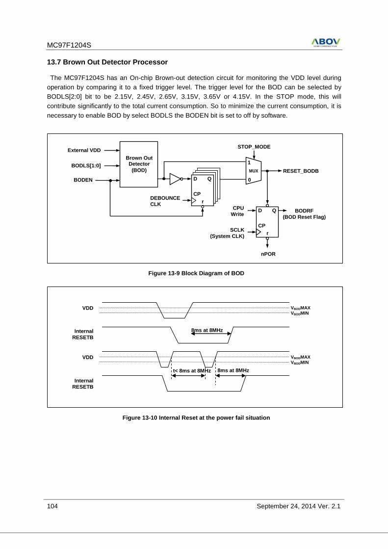
MC97F1204S
104 September 24, 2014 Ver. 2.1
13.7 Brown Out Detector Processor
The MC97F1204S has an On-chip Brown-out detection circuit for monitoring the VDD level during
operation by comparing it to a fixed trigger level. The trigger level for the BOD can be selected by
BODLS[2:0] bit to be 2.15V, 2.45V, 2.65V, 3.15V, 3.65V or 4.15V. In the STOP mode, this will
contribute significantly to the total current consumption. So to minimize the current consumption, it is
necessary to enable BOD by select BODLS the BODEN bit is set to off by software.
VDD
Internal
RESETB
VDD
Internal
RESETB
VBODMAX VBODMIN
8ms at 8MHz
t< 8ms at 8MHz 8ms at 8MHz
VBODMAX VBODMIN
BODLS[1:0] RESET_BODB
Brown Out Detector
(BOD)
D Q
CP
r
D Q
CP
r DEBOUNCE
CLK
External VDD
BODEN
BODRF
(BOD Reset Flag)
CPU
Write
SCLK
(System CLK)
nPOR
MUX
STOP_MODE
0
1
Figure 13-9 Block Diagram of BOD
Figure 13-10 Internal Reset at the power fail situation
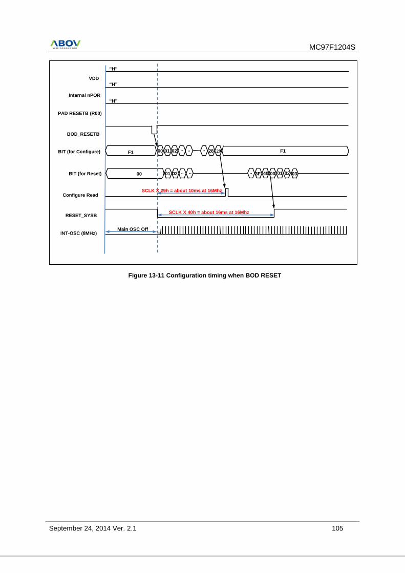
MC97F1204S
September 24, 2014 Ver. 2.1 105
VDD
Internal nPOR
PAD RESETB (R00)
BIT (for Configure)
BOD_RESETB
BIT (for Reset)
INT-OSC (8MHz)
RESET_SYSB
Configure Read SCLK X 29h = about 10ms at 16Mhz
SCLK X 40h = about 16ms at 16Mhz
F1 00 01 02
00 01 02
..
..
..
..
.. 28 29 F1
3F 40 00 01 02 03 ..
“H”
“H”
“H”
Main OSC Off
Figure 13-11 Configuration timing when BOD RESET
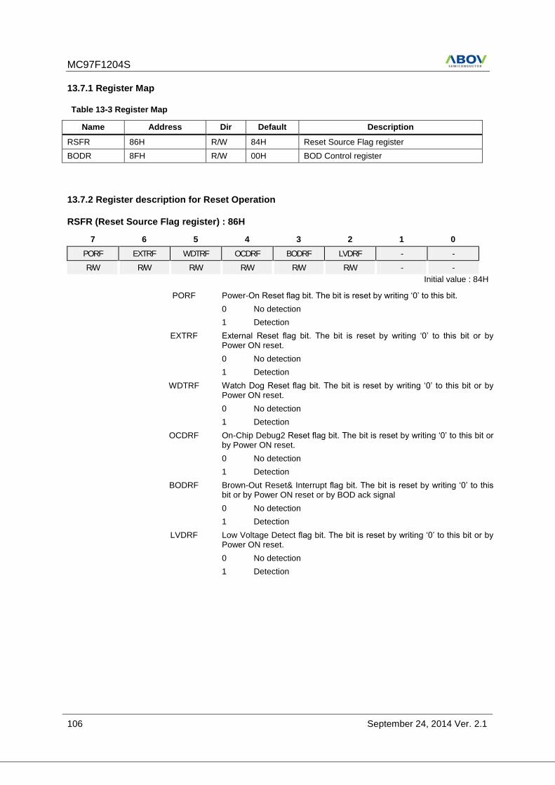
MC97F1204S
106 September 24, 2014 Ver. 2.1
13.7.1 Register Map
Table 13-3 Register Map
Name Address Dir Default Description
RSFR 86H R/W 84H Reset Source Flag register
BODR 8FH R/W 00H BOD Control register
13.7.2 Register description for Reset Operation
RSFR (Reset Source Flag register) : 86H
7 6 5 4 3 2 1 0
PORF EXTRF WDTRF OCDRF BODRF LVDRF - -
R/W R/W R/W R/W R/W R/W - -
Initial value : 84H
PORF Power-On Reset flag bit. The bit is reset by writing ‘0’ to this bit.
0 No detection
1 Detection
EXTRF External Reset flag bit. The bit is reset by writing ‘0’ to this bit or by Power ON reset.
0 No detection
1 Detection
WDTRF Watch Dog Reset flag bit. The bit is reset by writing ‘0’ to this bit or by Power ON reset.
0 No detection
1 Detection
OCDRF On-Chip Debug2 Reset flag bit. The bit is reset by writing ‘0’ to this bit or by Power ON reset.
0 No detection
1 Detection
BODRF Brown-Out Reset& Interrupt flag bit. The bit is reset by writing ‘0’ to this bit or by Power ON reset or by BOD ack signal
0 No detection
1 Detection
LVDRF Low Voltage Detect flag bit. The bit is reset by writing ‘0’ to this bit or by Power ON reset.
0 No detection
1 Detection
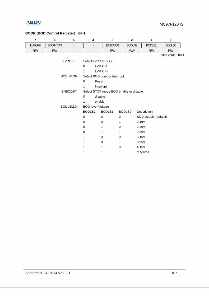
MC97F1204S
September 24, 2014 Ver. 2.1 107
BODR (BOD Control Register) : 8FH
7 6 5 4 3 2 1 0
LVROFF BODINTON - - ENBODST BODLS2 BODLS1 BODLS0
R/W R/W - - R/W R/W R/W R/W
Initial value : 00H
LVROFF Select LVR ON or OFF
0 LVR ON
1 LVR OFF
BODINTON Select BOD reset or Interrupt
0 Reset
1 Interrupt
ENBODST Select STOP mode BOD enable or disable
0 disable
1 enable
BODLS[2:0] BOD level Voltage
BODLS2 BODLS1 BODLS0 Description
0 0 0 BOD disable (default)
0 0 1 2.15V
0 1 0 2.45V
0 1 1 2.65V
1 0 0 3.15V
1 0 1 3.65V
1 1 0 4.15V
1 1 1 reserved
MC97F1204S
108 September 24, 2014 Ver. 2.1
14. On-chip Debug System
14.1 Overview
14.1.1 Description
On-chip debug System (OCD2) of MC97F1204OCD can be used for programming the non-volatile
memories and on-chip debugging. Detailed descriptions for programming via the OCD2 interface can
be found in the following chapter.
Figure 14-1 shows a block diagram of the OCD2 interface and the On-chip Debug system.
14.1.2 Feature
• Two-wire external interface: 1-wire serial clock input, 1-wire bi-directional serial data bus
• Debugger Access to:
− All Internal Peripheral Units
− Internal data RAM
− Program Counter
− Flash Memory
• Extensive On-chip Debug Support for Break Conditions, Including
− Break Instruction
− Single Step Break
− Program Memory Break Points on Single Address
− Programming of Flash, Fuses, and Lock Bits through the two-wire Interface
− On-chip Debugging Supported by OCD2 Dongle
• Operating frequency
Supports the maximum frequency of the target MCU
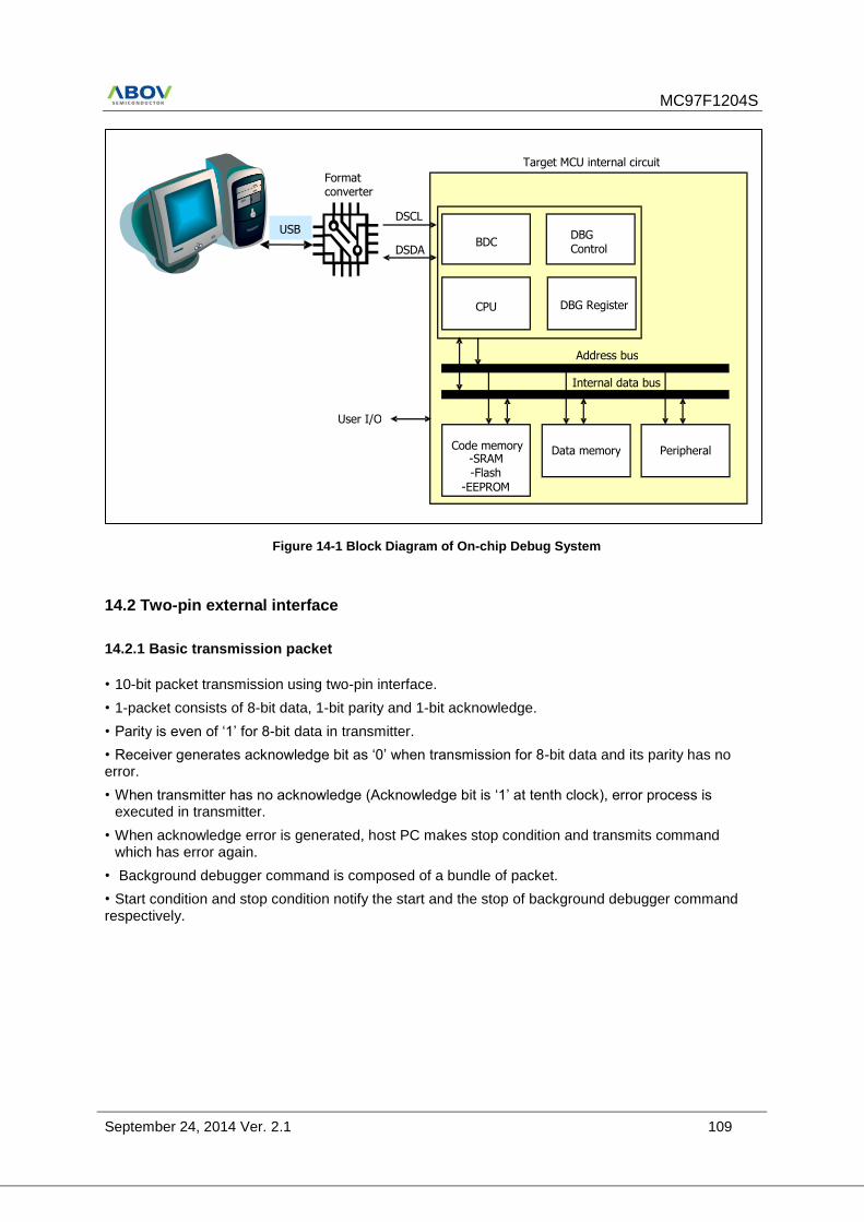
MC97F1204S
September 24, 2014 Ver. 2.1 109
14.2 Two-pin external interface
14.2.1 Basic transmission packet
• 10-bit packet transmission using two-pin interface.
• 1-packet consists of 8-bit data, 1-bit parity and 1-bit acknowledge.
• Parity is even of ‘1’ for 8-bit data in transmitter.
• Receiver generates acknowledge bit as ‘0’ when transmission for 8-bit data and its parity has no error.
• When transmitter has no acknowledge (Acknowledge bit is ‘1’ at tenth clock), error process is executed in transmitter.
• When acknowledge error is generated, host PC makes stop condition and transmits command which has error again.
• Background debugger command is composed of a bundle of packet.
• Start condition and stop condition notify the start and the stop of background debugger command respectively.
BDC
Format converter
USB
CPU
Code memory - SRAM - Flash
- EEPROM
Data memory
DBG Register
Peripheral
User I/O
Address bus
Internal data bus
DSDA
DSCL
Target MCU internal circuit
DBG Control
Figure 14-1 Block Diagram of On-chip Debug System
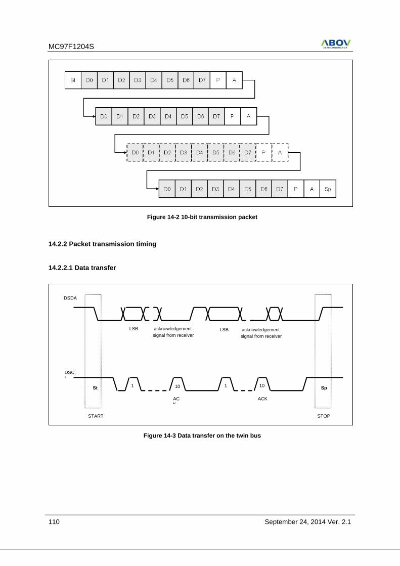
MC97F1204S
110 September 24, 2014 Ver. 2.1
14.2.2 Packet transmission timing
14.2.2.1 Data transfer
St Sp
START STOP
DSDA
DSCL
LSB acknowledgement signal from receiver
ACK
ACK
1 10 1 10
acknowledgement signal from receiver
LSB
Figure 14-2 10-bit transmission packet
Figure 14-3 Data transfer on the twin bus
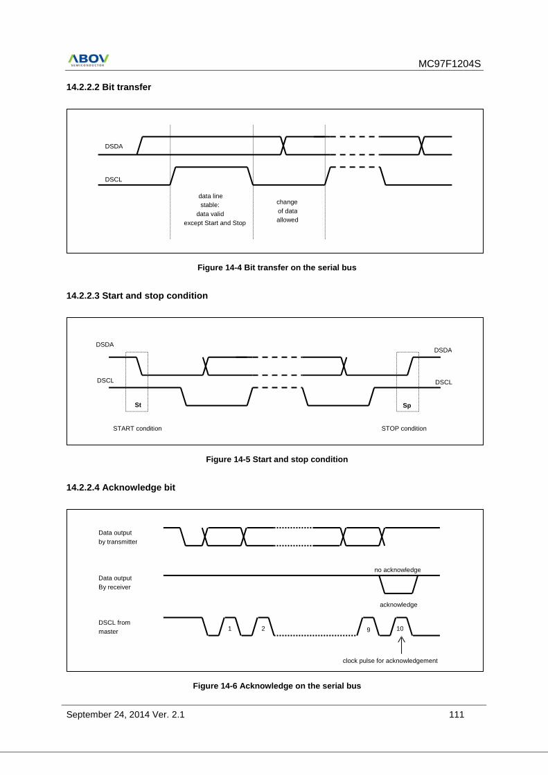
MC97F1204S
September 24, 2014 Ver. 2.1 111
14.2.2.2 Bit transfer
14.2.2.3 Start and stop condition
14.2.2.4 Acknowledge bit
1 9 2 10
Data output by transmitter
Data output By receiver
DSCL from master
clock pulse for acknowledgement
no acknowledge
acknowledge
St Sp
START condition STOP condition
DSDA
DSCL
DSDA
DSCL
data line stable:
data valid except Start and Stop
change of data allowed
DSDA
DSCL
Figure 14-4 Bit transfer on the serial bus
Figure 14-5 Start and stop condition
Figure 14-6 Acknowledge on the serial bus
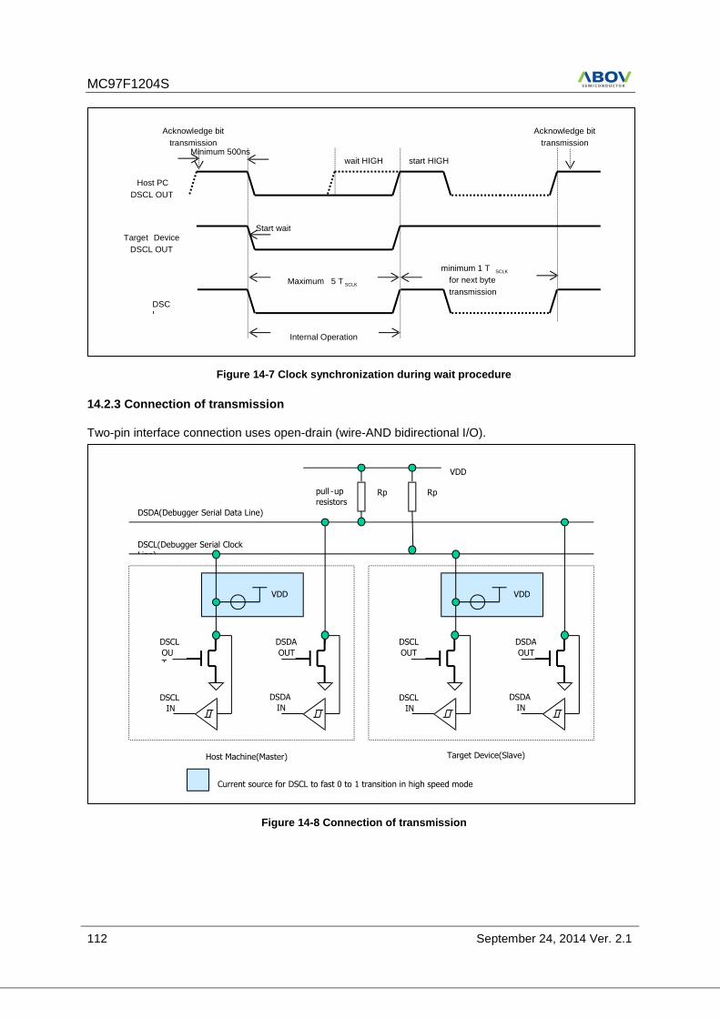
MC97F1204S
112 September 24, 2014 Ver. 2.1
14.2.3 Connection of transmission
Two-pin interface connection uses open-drain (wire-AND bidirectional I/O).
DSCL OU
T
DSDA OUT
DSDA IN
DSCL(Debugger Serial Clock
Line)
DSDA(Debugger Serial Data Line)
DSDA OUT
DSDA IN
Host Machine(Master) Target Device(Slave)
VDD VDD
Current source for DSCL to fast 0 to 1 transition in high speed mode
pull - up resistors
Rp Rp
VDD
DSCL IN
DSCL OUT
DSCL IN
Start wait
start HIGH
Host PC DSCL OUT
Target Device DSCL OUT
DSCL
wait HIGH
Maximum 5 T SCLK
Internal Operation
Acknowledge bit transmission
minimum 1 T SCLK for next byte transmission
Acknowledge bit transmission
Minimum 500ns
Figure 14-7 Clock synchronization during wait procedure
Figure 14-8 Connection of transmission
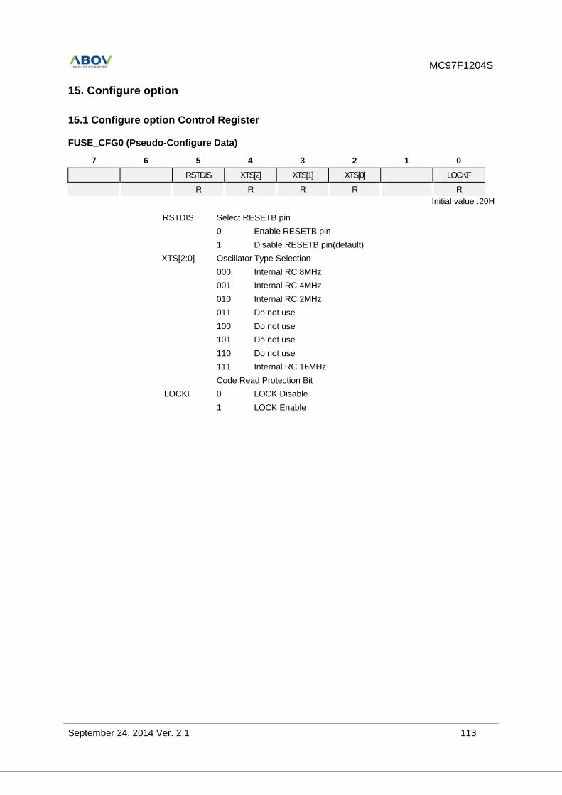
MC97F1204S
September 24, 2014 Ver. 2.1 113
15. Configure option
15.1 Configure option Control Register
FUSE_CFG0 (Pseudo-Configure Data)
7 6 5 4 3 2 1 0
RSTDIS XTS[2] XTS[1] XTS[0] LOCKF
R R R R R
Initial value :20H
RSTDIS Select RESETB pin
0 Enable RESETB pin
1 Disable RESETB pin(default)
XTS[2:0] Oscillator Type Selection
000 Internal RC 8MHz
001 Internal RC 4MHz
010 Internal RC 2MHz
011 Do not use
100 Do not use
101 Do not use
110 Do not use
111 Internal RC 16MHz
LOCKF
Code Read Protection Bit
0 LOCK Disable
1 LOCK Enable
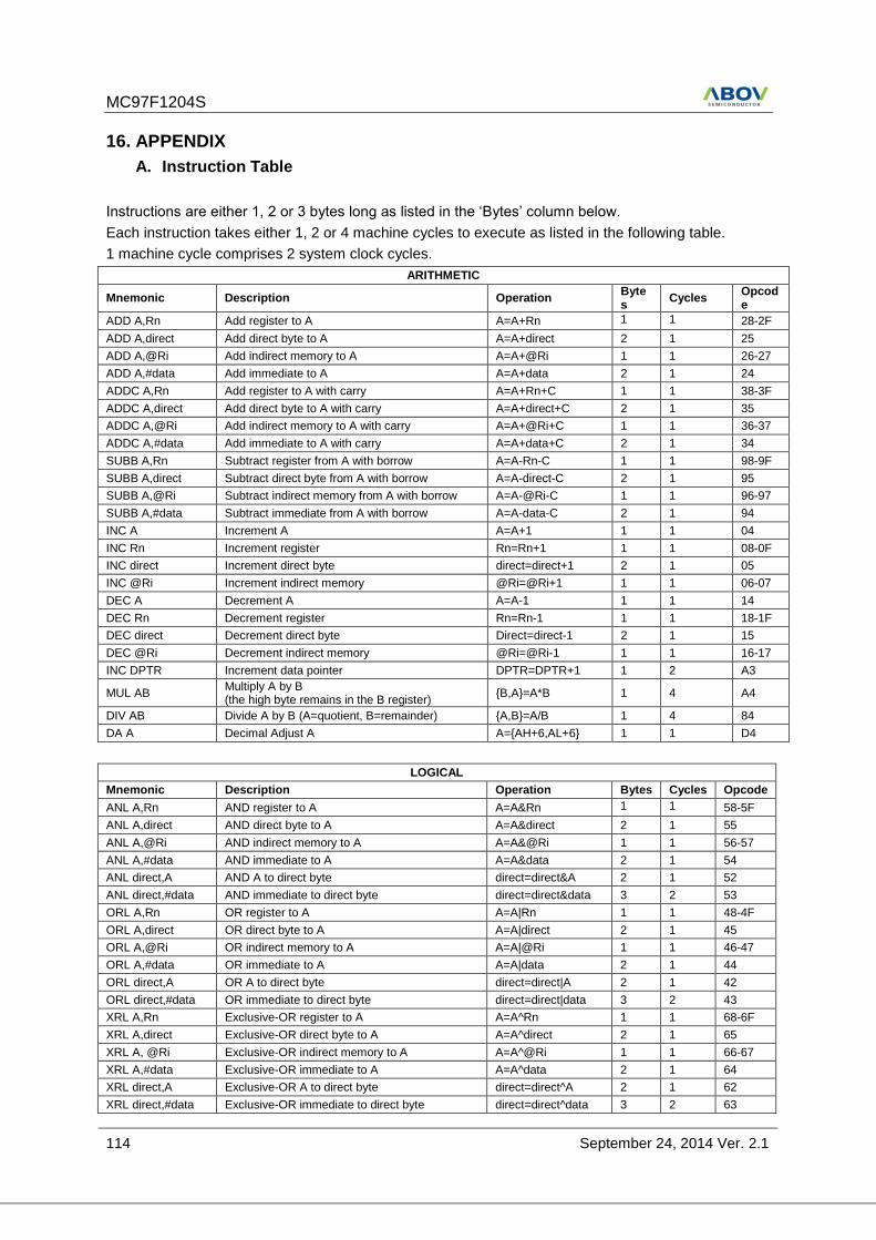
MC97F1204S
114 September 24, 2014 Ver. 2.1
16. APPENDIX
A. Instruction Table
Instructions are either 1, 2 or 3 bytes long as listed in the ‘Bytes’ column below.
Each instruction takes either 1, 2 or 4 machine cycles to execute as listed in the following table.
1 machine cycle comprises 2 system clock cycles.
ARITHMETIC
Mnemonic Description Operation Bytes
Cycles Opcode
ADD A,Rn Add register to A A=A+Rn 1 1 28-2F
ADD A,direct Add direct byte to A A=A+direct 2 1 25
ADD A,@Ri Add indirect memory to A A=A+@Ri 1 1 26-27
ADD A,#data Add immediate to A A=A+data 2 1 24
ADDC A,Rn Add register to A with carry A=A+Rn+C 1 1 38-3F
ADDC A,direct Add direct byte to A with carry A=A+direct+C 2 1 35
ADDC A,@Ri Add indirect memory to A with carry A=A+@Ri+C 1 1 36-37
ADDC A,#data Add immediate to A with carry A=A+data+C 2 1 34
SUBB A,Rn Subtract register from A with borrow A=A-Rn-C 1 1 98-9F
SUBB A,direct Subtract direct byte from A with borrow A=A-direct-C 2 1 95
SUBB A,@Ri Subtract indirect memory from A with borrow A=A-@Ri-C 1 1 96-97
SUBB A,#data Subtract immediate from A with borrow A=A-data-C 2 1 94
INC A Increment A A=A+1 1 1 04
INC Rn Increment register Rn=Rn+1 1 1 08-0F
INC direct Increment direct byte direct=direct+1 2 1 05
INC @Ri Increment indirect memory @Ri=@Ri+1 1 1 06-07
DEC A Decrement A A=A-1 1 1 14
DEC Rn Decrement register Rn=Rn-1 1 1 18-1F
DEC direct Decrement direct byte Direct=direct-1 2 1 15
DEC @Ri Decrement indirect memory @Ri=@Ri-1 1 1 16-17
INC DPTR Increment data pointer DPTR=DPTR+1 1 2 A3
MUL AB Multiply A by B (the high byte remains in the B register)
{B,A}=A*B 1 4 A4
DIV AB Divide A by B (A=quotient, B=remainder) {A,B}=A/B 1 4 84
DA A Decimal Adjust A A={AH+6,AL+6} 1 1 D4
LOGICAL
Mnemonic Description Operation Bytes Cycles Opcode
ANL A,Rn AND register to A A=A&Rn 1 1 58-5F
ANL A,direct AND direct byte to A A=A&direct 2 1 55
ANL A,@Ri AND indirect memory to A A=A&@Ri 1 1 56-57
ANL A,#data AND immediate to A A=A&data 2 1 54
ANL direct,A AND A to direct byte direct=direct&A 2 1 52
ANL direct,#data AND immediate to direct byte direct=direct&data 3 2 53
ORL A,Rn OR register to A A=A|Rn 1 1 48-4F
ORL A,direct OR direct byte to A A=A|direct 2 1 45
ORL A,@Ri OR indirect memory to A A=A|@Ri 1 1 46-47
ORL A,#data OR immediate to A A=A|data 2 1 44
ORL direct,A OR A to direct byte direct=direct|A 2 1 42
ORL direct,#data OR immediate to direct byte direct=direct|data 3 2 43
XRL A,Rn Exclusive-OR register to A A=A^Rn 1 1 68-6F
XRL A,direct Exclusive-OR direct byte to A A=A^direct 2 1 65
XRL A, @Ri Exclusive-OR indirect memory to A A=A^@Ri 1 1 66-67
XRL A,#data Exclusive-OR immediate to A A=A^data 2 1 64
XRL direct,A Exclusive-OR A to direct byte direct=direct^A 2 1 62
XRL direct,#data Exclusive-OR immediate to direct byte direct=direct^data 3 2 63
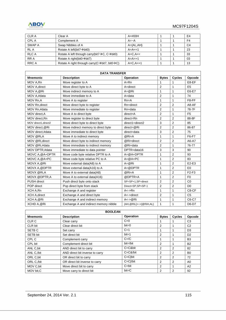
MC97F1204S
September 24, 2014 Ver. 2.1 115
CLR A Clear A A=#00H 1 1 E4
CPL A Complement A A=~A 1 1 F4
SWAP A Swap Nibbles of A A={AL,AH} 1 1 C4
RL A Rotate A left(bit7àbit0) A=A<<1 1 1 23
RLC A Rotate A left through carry(bit7àC, Càbit0) A=C,A<< 1 1 33
RR A Rotate A right(bit0àbit7) A=A>>1 1 1 03
RRC A Rotate A right through carry(Càbit7, bit0àC) A=C,A>>1 1 1 13
DATA TRANSFER
Mnemonic Description Operation Bytes Cycles Opcode
MOV A,Rn Move register to A A=Rn 1 1 E8-EF
MOV A,direct Move direct byte to A A=direct 2 1 E5
MOV A,@Ri Move indirect memory to A A=@Ri 1 1 E6-E7
MOV A,#data Move immediate to A A=data 2 1 74
MOV Rn,A Move A to register Rn=A 1 1 F8-FF
MOV Rn,direct Move direct byte to register Rn=direct 2 2 A8-AF
MOV Rn,#data Move immediate to register Rn=data 2 1 78-7F
MOV direct,A Move A to direct byte direct=A 2 1 F5
MOV direct,Rn Move register to direct byte direct=Rn 2 2 88-8F
MOV direct1,direct2 Move direct byte to direct byte direct1=direct2 3 2 85
MOV direct,@Ri Move indirect memory to direct byte direct=@Ri 2 2 86-87
MOV direct,#data Move immediate to direct byte direct=data 3 2 75
MOV @Ri,A Move A to indirect memory @Ri=A 1 1 F6-F7
MOV @Ri,direct Move direct byte to indirect memory @Ri=direct 2 2 A6-A7
MOV @Ri,#data Move immediate to indirect memory @Ri=data 2 1 76-77
MOV DPTR,#data Move immediate to data pointer DPTR=data16 3 3 90
MOVC A,@A+DPTR Move code byte relative DPTR to A A=@A+DPTR 1 2 93
MOVC A,@A+PC Move code byte relative PC to A A=@A+PC 1 2 83
MOVX A,@Ri Move external data(A8) to A A=@Ri 1 2 E2-E3
MOVX A,@DPTR Move external data(A16) to A A=@DPTR 1 2 E0
MOVX @Ri,A Move A to external data(A8) @Ri=A 1 2 F2-F3
MOVX @DPTR,A Move A to external data(A16) @DPTR=A 1 2 F0
PUSH direct Push direct byte onto stack SP=SP+1,SP=direct 2 2 C0
POP direct Pop direct byte from stack Direct=SP,SP=SP-1 2 2 D0
XCH A,Rn Exchange A and register A<->Rn 1 1 C8-CF
XCH A,direct Exchange A and direct byte A<->direct 2 1 C5
XCH A,@Ri Exchange A and indirect memory A<->@Ri 1 1 C6-C7
XCHD A,@Ri Exchange A and indirect memory nibble {AH,@RiL}<->{@RiH,AL} 1 1 D6-D7
BOOLEAN
Mnemonic Description Operation Bytes Cycles Opcode
CLR C Clear carry C=0 1 1 C3
CLR bit Clear direct bit bit=0 2 1 C2
SETB C Set carry C=1 1 1 D3
SETB bit Set direct bit bit=1 2 1 D2
CPL C Complement carry C=/C 1 1 B3
CPL bit Complement direct bit bit=/bit 2 1 B2
ANL C,bit AND direct bit to carry C=C&bit 2 2 82
ANL C,/bit AND direct bit inverse to carry C=C&/bit 2 2 B0
ORL C,bit OR direct bit to carry C=C|bit 2 2 72
ORL C,/bit OR direct bit inverse to carry C=C|/bit 2 2 A0
MOV C,bit Move direct bit to carry C=bit 2 1 A2
MOV bit,C Move carry to direct bit bit=C 2 2 92
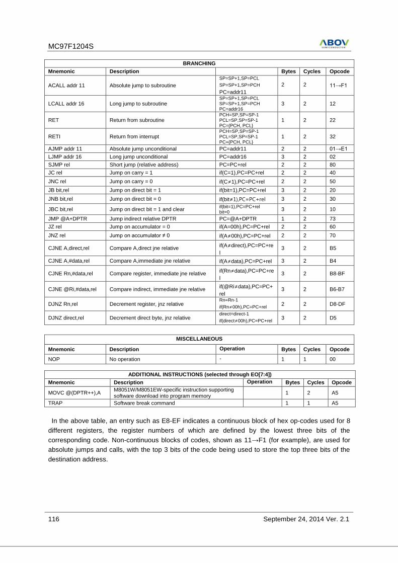
MC97F1204S
116 September 24, 2014 Ver. 2.1
BRANCHING
Mnemonic Description Bytes Cycles Opcode
ACALL addr 11 Absolute jump to subroutine
SP=SP+1,SP=PCL
SP=SP+1,SP=PCH
PC=addr11
2 2 11→F1
LCALL addr 16 Long jump to subroutine SP=SP+1,SP=PCL SP=SP+1,SP=PCH PC=addr16
3 2 12
RET Return from subroutine PCH=SP,SP=SP-1 PCL=SP,SP=SP-1 PC={PCH, PCL}
1 2 22
RETI Return from interrupt PCH=SP,SP=SP-1 PCL=SP,SP=SP-1 PC={PCH, PCL}
1 2 32
AJMP addr 11 Absolute jump unconditional PC=addr11 2 2 01→E1
LJMP addr 16 Long jump unconditional PC=addr16 3 2 02
SJMP rel Short jump (relative address) PC=PC+rel 2 2 80
JC rel Jump on carry = 1 if(C=1),PC=PC+rel 2 2 40
JNC rel Jump on carry = 0 if(C≠1),PC=PC+rel 2 2 50
JB bit,rel Jump on direct bit = 1 if(bit=1),PC=PC+rel 3 2 20
JNB bit,rel Jump on direct bit = 0 if(bit≠1),PC=PC+rel 3 2 30
JBC bit,rel Jump on direct bit = 1 and clear if(bit=1),PC=PC+rel bit=0 3 2 10
JMP @A+DPTR Jump indirect relative DPTR PC=@A+DPTR 1 2 73
JZ rel Jump on accumulator = 0 if(A=00h),PC=PC+rel 2 2 60
JNZ rel Jump on accumulator ≠ 0 if(A≠00h),PC=PC+rel 2 2 70
CJNE A,direct,rel Compare A,direct jne relative if(A≠direct),PC=PC+re
l 3 2 B5
CJNE A,#data,rel Compare A,immediate jne relative if(A≠data),PC=PC+rel 3 2 B4
CJNE Rn,#data,rel Compare register, immediate jne relative if(Rn≠data),PC=PC+re
l 3 2 B8-BF
CJNE @Ri,#data,rel Compare indirect, immediate jne relative if(@Ri≠data),PC=PC+
rel 3 2 B6-B7
DJNZ Rn,rel Decrement register, jnz relative Rn=Rn-1
if(Rn≠00h),PC=PC+rel 2 2 D8-DF
DJNZ direct,rel Decrement direct byte, jnz relative direct=direct-1
if(direct≠00h),PC=PC+rel 3 2 D5
MISCELLANEOUS
Mnemonic Description Operation Bytes Cycles Opcode
NOP No operation - 1 1 00
ADDITIONAL INSTRUCTIONS (selected through EO[7:4])
Mnemonic Description Operation Bytes Cycles Opcode
MOVC @(DPTR++),A M8051W/M8051EW-specific instruction supporting software download into program memory
1 2 A5
TRAP Software break command 1 1 A5
In the above table, an entry such as E8-EF indicates a continuous block of hex op-codes used for 8
different registers, the register numbers of which are defined by the lowest three bits of the
corresponding code. Non-continuous blocks of codes, shown as 11→F1 (for example), are used for
absolute jumps and calls, with the top 3 bits of the code being used to store the top three bits of the
destination address.
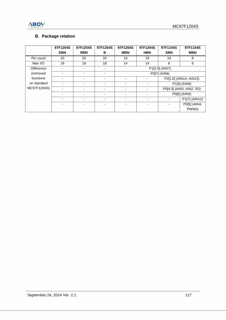
MC97F1204S
September 24, 2014 Ver. 2.1 117
B. Package relation
97F1204S
DBN
97F1204S
RBN
97F1204S
B
97F1204S
MBN
97F1204S
HBN
97F1104S
SBN
97F1104S
MBN
Pin count 20 20 20 16 16 10 8
Max I/O 18 18 18 14 14 8 6
Difference
(removed
functions
on standard
MC97F1204S)
- - - P1[2:0] (AIN7)
- - - P0[7] (AIN6)
- - - - - P2[1:0] (AIN14, AIN13)
- - - - - P1[4] (AIN9)
- - - - - P0[4:3] (AIN3, AIN2, SS)
- - - - - P0[6] (AIN5)
- - - - - - P1[7] (AIN12)
- - - - - - P0[5] (AIN4,
PWM2)