AD5755-1 (Rev. G) - analog.com · Quad Channel, 16-Bit, Serial Input, 4 mA to 20 mA and Voltage...
50
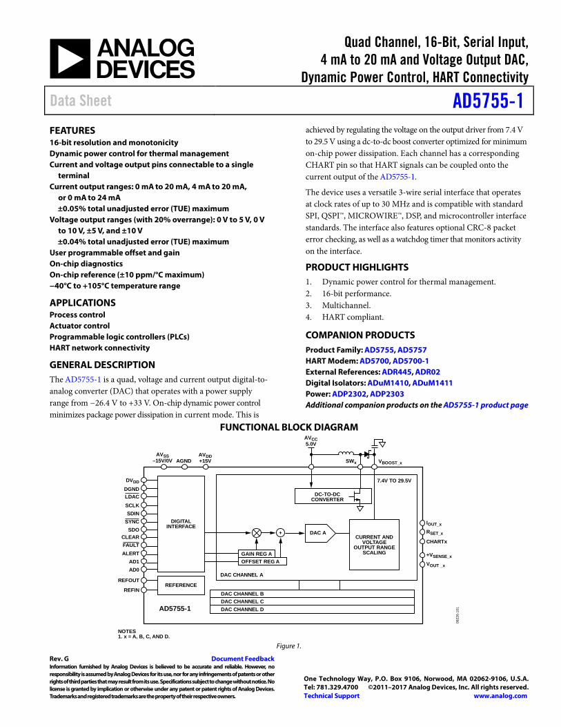
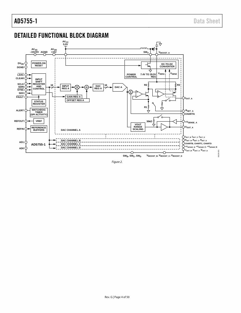
Quad Channel, 16-Bit, Serial Input, 4 mA to 20 mA and Voltage Output DAC, Dynamic Power Control, HART Connectivity Data Sheet AD5755-1 Rev. G Document Feedback Information furnished by Analog Devices is believed to be accurate and reliable. However, no responsibility is assumed by Analog Devices for its use, nor for any infringements of patents or other rights of third parties that may result from its use. Specifications subject to change without notice. No license is granted by implication or otherwise under any patent or patent rights of Analog Devices. Trademarks and registered trademarks are the property of their respective owners. One Technology Way, P.O. Box 9106, Norwood, MA 02062-9106, U.S.A. Tel: 781.329.4700 ©2011–2017 Analog Devices, Inc. All rights reserved. Technical Support www.analog.com FEATURES 16-bit resolution and monotonicity Dynamic power control for thermal management Current and voltage output pins connectable to a single terminal Current output ranges: 0 mA to 20 mA, 4 mA to 20 mA, or 0 mA to 24 mA ±0.05% total unadjusted error (TUE) maximum Voltage output ranges (with 20% overrange): 0 V to 5 V, 0 V to 10 V, ±5 V, and ±10 V ±0.04% total unadjusted error (TUE) maximum User programmable offset and gain On-chip diagnostics On-chip reference (±10 ppm/°C maximum) −40°C to +105°C temperature range APPLICATIONS Process control Actuator control Programmable logic controllers (PLCs) HART network connectivity GENERAL DESCRIPTION The AD5755-1 is a quad, voltage and current output digital-to- analog converter (DAC) that operates with a power supply range from −26.4 V to +33 V. On-chip dynamic power control minimizes package power dissipation in current mode. This is achieved by regulating the voltage on the output driver from 7.4 V to 29.5 V using a dc-to-dc boost converter optimized for minimum on-chip power dissipation. Each channel has a corresponding CHART pin so that HART signals can be coupled onto the current output of the AD5755-1. The device uses a versatile 3-wire serial interface that operates at clock rates of up to 30 MHz and is compatible with standard SPI, QSPI™, MICROWIRE™, DSP, and microcontroller interface standards. The interface also features optional CRC-8 packet error checking, as well as a watchdog timer that monitors activity on the interface. PRODUCT HIGHLIGHTS 1. Dynamic power control for thermal management. 2. 16-bit performance. 3. Multichannel. 4. HART compliant. COMPANION PRODUCTS Product Family: AD5755, AD5757 HART Modem: AD5700, AD5700-1 External References: ADR445, ADR02 Digital Isolators: ADuM1410, ADuM1411 Power: ADP2302, ADP2303 Additional companion products on the AD5755-1 product page FUNCTIONAL BLOCK DIAGRAM AD5755-1 09226-101 AV SS –15V/0V AGND AV DD +15V AV CC 5.0V DV DD DGND LDAC CLEAR SCLK SDIN SYNC SDO FAULT DC-TO-DC CONVERTER DIGITAL INTERFACE REFERENCE CURRENT AND VOLTAGE OUTPUT RANGE SCALING ALERT REFOUT REFIN NOTES 1. x = A, B, C, AND D. AD1 AD0 DAC A SW x V BOOST_x GAIN REG A OFFSET REG A R SET_x CHARTx +V SENSE_x V OUT _x I OUT_x DAC CHANNEL B DAC CHANNEL A DAC CHANNEL C DAC CHANNEL D 7.4V TO 29.5V + Figure 1.
Transcript of AD5755-1 (Rev. G) - analog.com · Quad Channel, 16-Bit, Serial Input, 4 mA to 20 mA and Voltage...
Quad Channel, 16-Bit, Serial Input, 4 mA to 20 mA and Voltage Output DAC,
Dynamic Power Control, HART Connectivity
Data Sheet AD5755-1
Rev. G Document Feedback Information furnished by Analog Devices is believed to be accurate and reliable. However, no responsibility is assumed by Analog Devices for its use, nor for any infringements of patents or other rights of third parties that may result from its use. Specifications subject to change without notice. No license is granted by implication or otherwise under any patent or patent rights of Analog Devices. Trademarks and registered trademarks are the property of their respective owners.
One Technology Way, P.O. Box 9106, Norwood, MA 02062-9106, U.S.A. Tel: 781.329.4700 ©2011–2017 Analog Devices, Inc. All rights reserved. Technical Support www.analog.com
FEATURES 16-bit resolution and monotonicity Dynamic power control for thermal management Current and voltage output pins connectable to a single
terminal Current output ranges: 0 mA to 20 mA, 4 mA to 20 mA,
or 0 mA to 24 mA ±0.05% total unadjusted error (TUE) maximum
Voltage output ranges (with 20% overrange): 0 V to 5 V, 0 V to 10 V, ±5 V, and ±10 V ±0.04% total unadjusted error (TUE) maximum
User programmable offset and gain On-chip diagnostics On-chip reference (±10 ppm/°C maximum) −40°C to +105°C temperature range
APPLICATIONS Process control Actuator control Programmable logic controllers (PLCs) HART network connectivity
GENERAL DESCRIPTION The AD5755-1 is a quad, voltage and current output digital-to-analog converter (DAC) that operates with a power supply range from −26.4 V to +33 V. On-chip dynamic power control minimizes package power dissipation in current mode. This is
achieved by regulating the voltage on the output driver from 7.4 V to 29.5 V using a dc-to-dc boost converter optimized for minimum on-chip power dissipation. Each channel has a corresponding CHART pin so that HART signals can be coupled onto the current output of the AD5755-1.
The device uses a versatile 3-wire serial interface that operates at clock rates of up to 30 MHz and is compatible with standard SPI, QSPI™, MICROWIRE™, DSP, and microcontroller interface standards. The interface also features optional CRC-8 packet error checking, as well as a watchdog timer that monitors activity on the interface.
PRODUCT HIGHLIGHTS 1. Dynamic power control for thermal management. 2. 16-bit performance. 3. Multichannel. 4. HART compliant.
COMPANION PRODUCTS Product Family: AD5755, AD5757 HART Modem: AD5700, AD5700-1 External References: ADR445, ADR02 Digital Isolators: ADuM1410, ADuM1411 Power: ADP2302, ADP2303 Additional companion products on the AD5755-1 product page
FUNCTIONAL BLOCK DIAGRAM
AD5755-1
0922
6-10
1AVSS
–15V/0V AGNDAVDD+15V
AVCC5.0V
DVDDDGNDLDAC
CLEAR
SCLKSDIN
SYNCSDO
FAULT
DC-TO-DCCONVERTER
DIGITALINTERFACE
REFERENCE
CURRENT ANDVOLTAGE
OUTPUT RANGESCALINGALERT
REFOUT
REFIN
NOTES1. x = A, B, C, AND D.
AD1AD0
DAC A
SWx VBOOST_x
GAIN REG AOFFSET REG A
RSET_x
CHARTx
+VSENSE_x
VOUT _x
IOUT_x
DAC CHANNEL B
DAC CHANNEL A
DAC CHANNEL CDAC CHANNEL D
7.4V TO 29.5V
+
Figure 1.
AD5755-1 Data Sheet
Rev. G | Page 2 of 50
TABLE OF CONTENTS Features .............................................................................................. 1 Applications ....................................................................................... 1 General Description ......................................................................... 1 Product Highlights ........................................................................... 1 Companion Products ....................................................................... 1 Functional Block Diagram .............................................................. 1 Revision History ............................................................................... 3 Detailed Functional Block Diagram .............................................. 4 Specifications ..................................................................................... 5
AC Performance Characteristics ................................................ 8 Timing Characteristics ................................................................ 9
Absolute Maximum Ratings .......................................................... 12 ESD Caution ................................................................................ 12
Pin Configuration and Function Descriptions ........................... 13 Typical Performance Characteristics ........................................... 16
Voltage Outputs .......................................................................... 16 Current Outputs ......................................................................... 20 DC-to-DC Block ......................................................................... 24 Reference ..................................................................................... 25 General ......................................................................................... 26
Terminology .................................................................................... 27 Theory of Operation ...................................................................... 29
DAC Architecture ....................................................................... 29 Power-On State of the AD5755-1 ............................................. 29 Serial Interface ............................................................................ 30 Transfer Function ....................................................................... 30
Registers ........................................................................................... 31 Programming Sequence to Write/Enable the Output Correctly ...................................................................................... 32 Changing and Reprogramming the Range ............................. 32 Data Registers ............................................................................. 33 Control Registers ........................................................................ 35
Readback Operation .................................................................. 38 Device Features ............................................................................... 40
Output Fault ................................................................................ 40 Voltage Output Short-Circuit Protection ................................ 40 Digital Offset and Gain Control ............................................... 40 Status Readback During a Write .............................................. 40 Asynchronous Clear ................................................................... 41 Packet Error Checking ............................................................... 41 Watchdog Timer ......................................................................... 41 Output Alert ................................................................................ 41 Internal Reference ...................................................................... 41 External Current Setting Resistor ............................................ 41 HART Connectivity ................................................................... 42 Digital Slew Rate Control .......................................................... 42 Power Dissipation control ......................................................... 43 DC-to-DC Converters ............................................................... 43 AICC Supply Requirements—Static .......................................... 44 AICC Supply Requirements—Slewing ...................................... 44
Applications Information .............................................................. 46 Voltage and Current Output Ranges on the Same Terminal 46 Current Output Mode with Internal RSET ................................ 46 Precision Voltage Reference Selection ..................................... 46 Driving Inductive Loads ............................................................ 47 Transient Voltage Protection .................................................... 47 Microprocessor Interfacing ....................................................... 47 Layout Guidelines....................................................................... 47 Galvanically Isolated Interface ................................................. 48 Industrial HART Capable Analog Output Application—Shared VOUT_x and IOUT_x Pin ...................................................... 49
Outline Dimensions ....................................................................... 50 Ordering Guide .......................................................................... 50
Data Sheet AD5755-1
Rev. G | Page 3 of 50
REVISION HISTORY 4/2017—Rev. F to Rev. G
Changes to Table 1, DICC Parameter ............................................... 8 Changes to Table 3 ............................................................................ 9 Changes to Figure 3 and Figure 4 .................................................. 10 Changes to Figure 5 ......................................................................... 11 Changes to the Readback Operation Section .............................. 38 Deleted Table 28 and Table 29, Renumbered Sequentially ........ 38 Changes to Status Readback During a Write Section ................. 40 Changes to Packet Error Checking Section ................................. 41 Updated Outline Dimensions ........................................................ 50
9/2014—Rev. E to Rev. F
Changes to Thermal Hysteresis Parameter, Table 1 ...................... 7 Changes to Table 3 ............................................................................ 9 Changes to Figure 4 ......................................................................... 10 Added Figure 5; Renumbered Sequentially ................................. 11 Changes to Table 5 .......................................................................... 14 Changes to Figure 56 through Figure 59 ...................................... 24 Change to Figure 70 and Figure 71 ............................................... 26 Change to Voltage Reference Thermal Hysteresis Definition ........ 27 Changes to Table 7 .......................................................................... 31 Changes to Offset Register Section, Table 12, and Table 14 ...... 34 Changes to Software Register Section, Table 22, and Table 23 ....... 37 Changes to Readback Operation Section, Added Table 28 and Table 29; Renumbered Sequentially .............................................. 38 Changes to Status Register Section, Table 31, and Table 32 ...... 40 Changes to Status Readback During a Write Section ................. 41 Changes to Packet Error Checking Section ................................. 42 Changes to HART Connectivity Section ...................................... 43 Changes to Table 36 ........................................................................ 44
11/2012—Rev. D to Rev. E
Changes to Figure 2 ........................................................................... 4 Changed Thermal Impedance from 20°C/W to 28°C/W .......... 12 Changes to Pin 6 Description ........................................................ 13 Changes to Pin 27 Description ...................................................... 14 Changes to Figure 26 ...................................................................... 19 Changes to DUT_AD1, DUT_AD0 Description, Table 9 ......... 33 Changes to Packet Error Checking Section and Internal Reference Section ............................................................................ 41 Changes to Figure 81 ...................................................................... 43 Changes to Figure 86 ...................................................................... 47 Changes to Figure 89 ...................................................................... 49
7/2012—Rev. C to Rev. D
Changes to Figure 89 ...................................................................... 49 Updated Outline Dimensions ........................................................ 50
5/2012—Rev. B to Rev. C
Changes to Companion Products Section ..................................... 1 Changes to Figure 2 .......................................................................... 3 Changes to Table 5 .......................................................................... 15 Changes to Figure 22 ...................................................................... 18 Added Industrial HART Capable Analog Output Application—Shared VOUT_x and IOUT_X Pin Section and Figure 89, Renumbered Sequentially .............................................................. 49 Updated Outline Dimensions ........................................................ 50
11/2011—Rev. A to Rev. B
Removed Voltage Output Test Conditions/Comments, Table 1 .... 5 Changed Headroom and Footroom Test Conditions/Comments, Table 1 .......................................................................................................... 5 Changes to Figure 4 ........................................................................ 10 Changes to Figure 5 ........................................................................ 11 Changes to SCLK Description, Table 5 ........................................ 13 Changes to Figure 12 ...................................................................... 16 Changes to Figure 21 ...................................................................... 18 Changes to Figure 37 ...................................................................... 20 Changes to Figure 44 ...................................................................... 22 Changes to Figure 71 ...................................................................... 29 Changes to Power-On State of the AD5755-1 Section ............... 30 Changes to Table 17 ........................................................................ 35 Changes to Readback Operation section and Table 26 .............. 38 Changes to Voltage Output Short-Circuit Protection Section .. 40 Changes to Figure 78 ...................................................................... 41 Changes to Figure 82 ...................................................................... 44 Changes to Figure 83, Figure 84, and Figure 85 ................................. 45 Changes to Transient Voltage Protection Section and Figure 86 ... 47 Changes to Galvanically Isolated Interface Section .................... 48
5/2011—Rev. 0 to Rev. A
Removed Endnote 6 (Table 1) ......................................................... 6 Changed AVDD Minimum Value from 10.8 V to 9 V .................... 6 Changed AISS Minimum Value from −1.4 mA to −1.7 mA ......... 7 Changed AVDD Voltage in Pin 19 Description ............................. 13 Changes to Ordering Guide ........................................................... 48
4/2011—Revision 0: Initial Version
AD5755-1 Data Sheet
Rev. G | Page 4 of 50
DETAILED FUNCTIONAL BLOCK DIAGRAM
AD5755-1
0922
6-00
1
AVSS–15V/0V AGND
AVDD+15V
AVCC5.0V
DVDDDGND
LDACCLEAR
SCLKSDIN
SYNCSDO
FAULT
DC-TO-DCCONVERTER
POWERCONTROL
INPUTSHIFT
REGISTERAND
CONTROL
STATUSREGISTER
POWER-ONRESET
REFERENCEBUFFERS
DACREG A
INPUTREG A
VREF
WATCHDOGTIMER
(SPI ACTIVITY)
VOUTRANGE
SCALING
ALERT
REFOUT
REFIN
AD1
AD0
DAC A1616
SWA VBOOST_A
GAIN REG AOFFSET REG A
R1
R2 R3
RSET_ACHARTA
+VSENSE_A
VOUT_A
IOUT_B, IOUT_C, IOUT_D
RSET_B, RSET_C, RSET_D
CHARTB, CHARTC, CHARTD+VSENSE_B, +VSENSE_C, +VSENSE_DVOUT_B, VOUT_C, VOUT_D
IOUT_A
DAC CHANNEL B
DAC CHANNEL A
DAC CHANNEL CDAC CHANNEL D
SWB, SWC, SWD VBOOST_B, VBOOST_C, VBOOST_D
7.4V TO 29.5VREG
VSEN1 VSEN2
30kΩ
Figure 2.
Data Sheet AD5755-1
Rev. G | Page 5 of 50
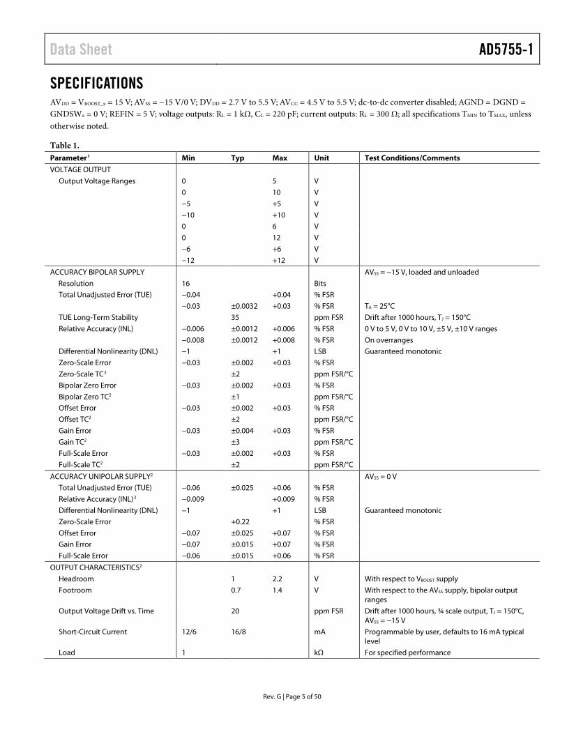
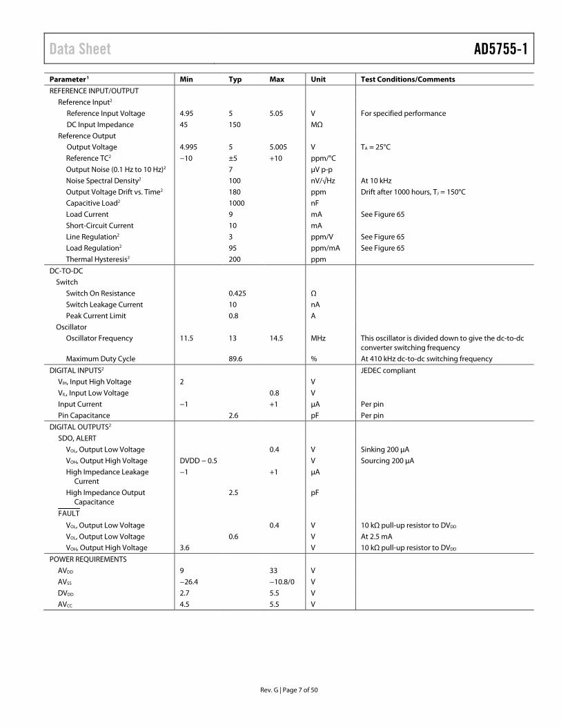
SPECIFICATIONS AVDD = VBOOST_x = 15 V; AVSS = −15 V/0 V; DVDD = 2.7 V to 5.5 V; AVCC = 4.5 V to 5.5 V; dc-to-dc converter disabled; AGND = DGND = GNDSWx = 0 V; REFIN = 5 V; voltage outputs: RL = 1 kΩ, CL = 220 pF; current outputs: RL = 300 Ω; all specifications TMIN to TMAX, unless otherwise noted.
Table 1. Parameter1 Min Typ Max Unit Test Conditions/Comments VOLTAGE OUTPUT
Output Voltage Ranges 0 5 V 0 10 V −5 +5 V −10 +10 V 0 6 V 0 12 V −6 +6 V −12 +12 V
ACCURACY BIPOLAR SUPPLY AVSS = −15 V, loaded and unloaded Resolution 16 Bits Total Unadjusted Error (TUE) −0.04 +0.04 % FSR
−0.03 ±0.0032 +0.03 % FSR TA = 25°C TUE Long-Term Stability 35 ppm FSR Drift after 1000 hours, TJ = 150°C Relative Accuracy (INL) −0.006 ±0.0012 +0.006 % FSR 0 V to 5 V, 0 V to 10 V, ±5 V, ±10 V ranges
−0.008 ±0.0012 +0.008 % FSR On overranges Differential Nonlinearity (DNL) −1 +1 LSB Guaranteed monotonic Zero-Scale Error −0.03 ±0.002 +0.03 % FSR Zero-Scale TC2 ±2 ppm FSR/°C Bipolar Zero Error −0.03 ±0.002 +0.03 % FSR Bipolar Zero TC2 ±1 ppm FSR/°C Offset Error −0.03 ±0.002 +0.03 % FSR Offset TC2 ±2 ppm FSR/°C Gain Error −0.03 ±0.004 +0.03 % FSR Gain TC2 ±3 ppm FSR/°C Full-Scale Error −0.03 ±0.002 +0.03 % FSR Full-Scale TC2 ±2 ppm FSR/°C
ACCURACY UNIPOLAR SUPPLY2 AVSS = 0 V Total Unadjusted Error (TUE) −0.06 ±0.025 +0.06 % FSR Relative Accuracy (INL)3 −0.009 +0.009 % FSR Differential Nonlinearity (DNL) −1 +1 LSB Guaranteed monotonic Zero-Scale Error +0.22 % FSR Offset Error −0.07 ±0.025 +0.07 % FSR Gain Error −0.07 ±0.015 +0.07 % FSR Full-Scale Error −0.06 ±0.015 +0.06 % FSR
OUTPUT CHARACTERISTICS2 Headroom 1 2.2 V With respect to VBOOST supply Footroom 0.7 1.4 V With respect to the AVSS supply, bipolar output
ranges Output Voltage Drift vs. Time 20 ppm FSR Drift after 1000 hours, ¾ scale output, TJ = 150°C,
AVSS = −15 V Short-Circuit Current 12/6 16/8 mA Programmable by user, defaults to 16 mA typical
level Load 1 kΩ For specified performance
AD5755-1 Data Sheet
Rev. G | Page 6 of 50
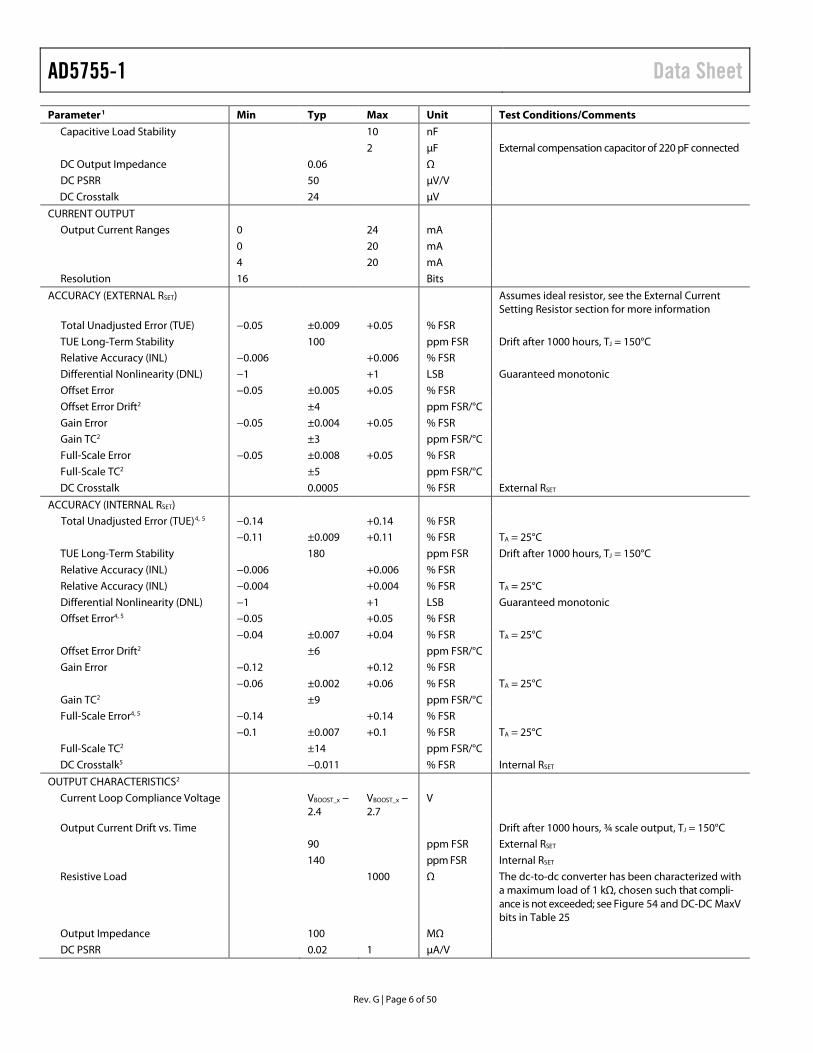
Parameter1 Min Typ Max Unit Test Conditions/Comments Capacitive Load Stability 10 nF
2 µF External compensation capacitor of 220 pF connected DC Output Impedance 0.06 Ω DC PSRR 50 µV/V DC Crosstalk 24 µV
CURRENT OUTPUT Output Current Ranges 0 24 mA
0 20 mA 4 20 mA
Resolution 16 Bits ACCURACY (EXTERNAL RSET) Assumes ideal resistor, see the External Current
Setting Resistor section for more information Total Unadjusted Error (TUE) −0.05 ±0.009 +0.05 % FSR TUE Long-Term Stability 100 ppm FSR Drift after 1000 hours, TJ = 150°C Relative Accuracy (INL) −0.006 +0.006 % FSR Differential Nonlinearity (DNL) −1 +1 LSB Guaranteed monotonic Offset Error −0.05 ±0.005 +0.05 % FSR Offset Error Drift2 ±4 ppm FSR/°C Gain Error −0.05 ±0.004 +0.05 % FSR Gain TC2 ±3 ppm FSR/°C Full-Scale Error −0.05 ±0.008 +0.05 % FSR Full-Scale TC2 ±5 ppm FSR/°C DC Crosstalk 0.0005 % FSR External RSET
ACCURACY (INTERNAL RSET) Total Unadjusted Error (TUE)4, 5 −0.14 +0.14 % FSR
−0.11 ±0.009 +0.11 % FSR TA = 25°C TUE Long-Term Stability 180 ppm FSR Drift after 1000 hours, TJ = 150°C Relative Accuracy (INL) −0.006 +0.006 % FSR Relative Accuracy (INL) −0.004 +0.004 % FSR TA = 25°C Differential Nonlinearity (DNL) −1 +1 LSB Guaranteed monotonic Offset Error4, 5 −0.05 +0.05 % FSR
−0.04 ±0.007 +0.04 % FSR TA = 25°C Offset Error Drift2 ±6 ppm FSR/°C Gain Error −0.12 +0.12 % FSR
−0.06 ±0.002 +0.06 % FSR TA = 25°C Gain TC2 ±9 ppm FSR/°C Full-Scale Error4, 5 −0.14 +0.14 % FSR
−0.1 ±0.007 +0.1 % FSR TA = 25°C Full-Scale TC2 ±14 ppm FSR/°C DC Crosstalk5 −0.011 % FSR Internal RSET
OUTPUT CHARACTERISTICS2 Current Loop Compliance Voltage VBOOST_x −
2.4 VBOOST_x − 2.7
V
Output Current Drift vs. Time Drift after 1000 hours, ¾ scale output, TJ = 150°C 90 ppm FSR External RSET 140 ppm FSR Internal RSET
Resistive Load 1000 Ω The dc-to-dc converter has been characterized with a maximum load of 1 kΩ, chosen such that compli-ance is not exceeded; see Figure 54 and DC-DC MaxV bits in Table 25
Output Impedance 100 MΩ DC PSRR 0.02 1 µA/V
Data Sheet AD5755-1
Rev. G | Page 7 of 50
Parameter1 Min Typ Max Unit Test Conditions/Comments REFERENCE INPUT/OUTPUT
Reference Input2 Reference Input Voltage 4.95 5 5.05 V For specified performance DC Input Impedance 45 150 MΩ
Reference Output Output Voltage 4.995 5 5.005 V TA = 25°C Reference TC2 −10 ±5 +10 ppm/°C Output Noise (0.1 Hz to 10 Hz)2 7 µV p-p Noise Spectral Density2 100 nV/√Hz At 10 kHz Output Voltage Drift vs. Time2 180 ppm Drift after 1000 hours, TJ = 150°C Capacitive Load2 1000 nF Load Current 9 mA See Figure 65 Short-Circuit Current 10 mA Line Regulation2 3 ppm/V See Figure 65 Load Regulation2 95 ppm/mA See Figure 65 Thermal Hysteresis2 200 ppm
DC-TO-DC Switch
Switch On Resistance 0.425 Ω Switch Leakage Current 10 nA Peak Current Limit 0.8 A
Oscillator Oscillator Frequency 11.5 13 14.5 MHz This oscillator is divided down to give the dc-to-dc
converter switching frequency Maximum Duty Cycle 89.6 % At 410 kHz dc-to-dc switching frequency
DIGITAL INPUTS2 JEDEC compliant VIH, Input High Voltage 2 V VIL, Input Low Voltage 0.8 V Input Current −1 +1 µA Per pin Pin Capacitance 2.6 pF Per pin
DIGITAL OUTPUTS2 SDO, ALERT
VOL, Output Low Voltage 0.4 V Sinking 200 µA VOH, Output High Voltage DVDD − 0.5 V Sourcing 200 µA High Impedance Leakage
Current −1 +1 µA
High Impedance Output Capacitance
2.5 pF
FAULT VOL, Output Low Voltage 0.4 V 10 kΩ pull-up resistor to DVDD VOL, Output Low Voltage 0.6 V At 2.5 mA VOH, Output High Voltage 3.6 V 10 kΩ pull-up resistor to DVDD
POWER REQUIREMENTS AVDD 9 33 V AVSS −26.4 −10.8/0 V DVDD 2.7 5.5 V AVCC 4.5 5.5 V
AD5755-1 Data Sheet
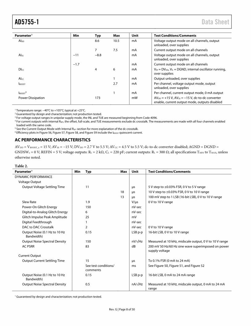
Rev. G | Page 8 of 50
Parameter1 Min Typ Max Unit Test Conditions/Comments AIDD 8.6 10.5 mA Voltage output mode on all channels, output
unloaded, over supplies 7 7.5 mA Current output mode on all channels
AISS −11 −8.8 mA Voltage output mode on all channels, output unloaded, over supplies
−1.7 mA Current output mode on all channels DICC 4 6 mA VIH = DVDD, VIL = DGND, internal oscillator running,
over supplies AICC 1 mA Output unloaded, over supplies IBOOST 2.7 mA Per channel, voltage output mode, output
unloaded, over supplies IBOOST
6 1 mA Per channel, current output mode, 0 mA output Power Dissipation 173 mW AVDD = +15 V, AVSS = −15 V, dc-to-dc converter
enable, current output mode, outputs disabled
1 Temperature range: −40°C to +105°C; typical at +25°C. 2 Guaranteed by design and characterization; not production tested. 3 For voltage output ranges in unipolar supply mode, the INL and TUE are measured beginning from Code 4096. 4 For current outputs with internal RSET, the offset, full-scale, and TUE measurements exclude dc crosstalk. The measurements are made with all four channels enabled
loaded with the same code. 5 See the Current Output Mode with Internal RSET section for more explanation of the dc crosstalk. 6 Efficiency plots in Figure 56, Figure 57, Figure 58, and Figure 59 include the IBOOST quiescent current.
AC PERFORMANCE CHARACTERISTICS AVDD = VBOOST_x = 15 V; AVSS = −15 V; DVDD = 2.7 V to 5.5 V; AVCC = 4.5 V to 5.5 V; dc-to-dc converter disabled; AGND = DGND = GNDSWx = 0 V; REFIN = 5 V; voltage outputs: RL = 2 kΩ, CL = 220 pF; current outputs: RL = 300 Ω; all specifications TMIN to TMAX, unless otherwise noted.
Table 2. Parameter1 Min Typ Max Unit Test Conditions/Comments DYNAMIC PERFORMANCE
Voltage Output Output Voltage Settling Time 11 µs 5 V step to ±0.03% FSR, 0 V to 5 V range
18 µs 10 V step to ±0.03% FSR, 0 V to 10 V range 13 µs 100 mV step to 1 LSB (16-bit LSB), 0 V to 10 V range
Slew Rate 1.9 V/µs 0 V to 10 V range Power-On Glitch Energy 150 nV-sec Digital-to-Analog Glitch Energy 6 nV-sec Glitch Impulse Peak Amplitude 25 mV Digital Feedthrough 1 nV-sec DAC to DAC Crosstalk 2 nV-sec 0 V to 10 V range Output Noise (0.1 Hz to 10 Hz
Bandwidth) 0.15 LSB p-p 16-bit LSB, 0 V to 10 V range
Output Noise Spectral Density 150 nV/√Hz Measured at 10 kHz, midscale output, 0 V to 10 V range AC PSRR 83 dB 200 mV 50 Hz/60 Hz sine wave superimposed on power
supply voltage Current Output
Output Current Settling Time 15 µs To 0.1% FSR (0 mA to 24 mA) See test conditions/ comments
ms See Figure 50, Figure 51, and Figure 52
Output Noise (0.1 Hz to 10 Hz Bandwidth)
0.15 LSB p-p 16-bit LSB, 0 mA to 24 mA range
Output Noise Spectral Density 0.5 nA/√Hz Measured at 10 kHz, midscale output, 0 mA to 24 mA range
1 Guaranteed by design and characterization; not production tested.
Data Sheet AD5755-1
Rev. G | Page 9 of 50
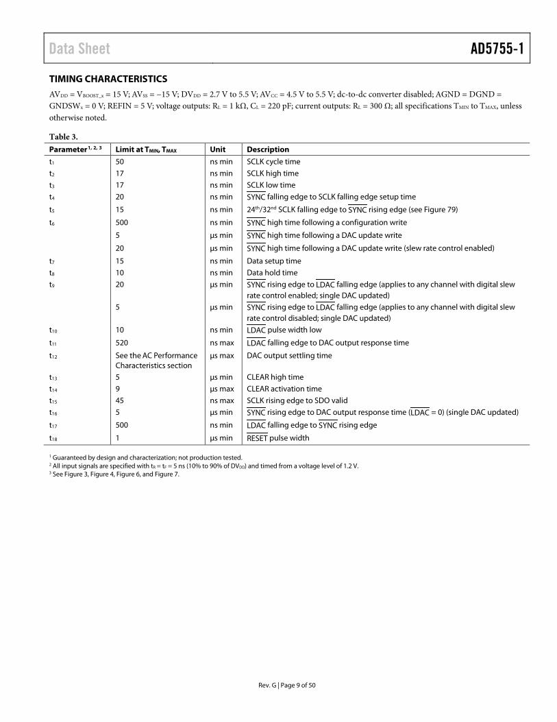
TIMING CHARACTERISTICS AVDD = VBOOST_x = 15 V; AVSS = −15 V; DVDD = 2.7 V to 5.5 V; AVCC = 4.5 V to 5.5 V; dc-to-dc converter disabled; AGND = DGND = GNDSWx = 0 V; REFIN = 5 V; voltage outputs: RL = 1 kΩ, CL = 220 pF; current outputs: RL = 300 Ω; all specifications TMIN to TMAX, unless otherwise noted.
Table 3. Parameter1, 2, 3 Limit at TMIN, TMAX Unit Description t1 50 ns min SCLK cycle time t2 17 ns min SCLK high time t3 17 ns min SCLK low time t4 20 ns min SYNC falling edge to SCLK falling edge setup time
t5 15 ns min 24th/32nd SCLK falling edge to SYNC rising edge (see Figure 79)
t6 500 ns min SYNC high time following a configuration write
5 µs min SYNC high time following a DAC update write
20 µs min SYNC high time following a DAC update write (slew rate control enabled)
t7 15 ns min Data setup time t8 10 ns min Data hold time t9 20 µs min SYNC rising edge to LDAC falling edge (applies to any channel with digital slew
rate control enabled; single DAC updated) 5 µs min SYNC rising edge to LDAC falling edge (applies to any channel with digital slew
rate control disabled; single DAC updated) t10 10 ns min LDAC pulse width low
t11 520 ns max LDAC falling edge to DAC output response time
t12 See the AC Performance Characteristics section
µs max DAC output settling time
t13 5 µs min CLEAR high time t14 9 µs max CLEAR activation time t15 45 ns max SCLK rising edge to SDO valid t16 5 µs min SYNC rising edge to DAC output response time (LDAC = 0) (single DAC updated)
t17 500 ns min LDAC falling edge to SYNC rising edge
t18 1 µs min RESET pulse width
1 Guaranteed by design and characterization; not production tested. 2 All input signals are specified with tR = tF = 5 ns (10% to 90% of DVDD) and timed from a voltage level of 1.2 V. 3 See Figure 3, Figure 4, Figure 6, and Figure 7.
AD5755-1 Data Sheet
Rev. G | Page 10 of 50
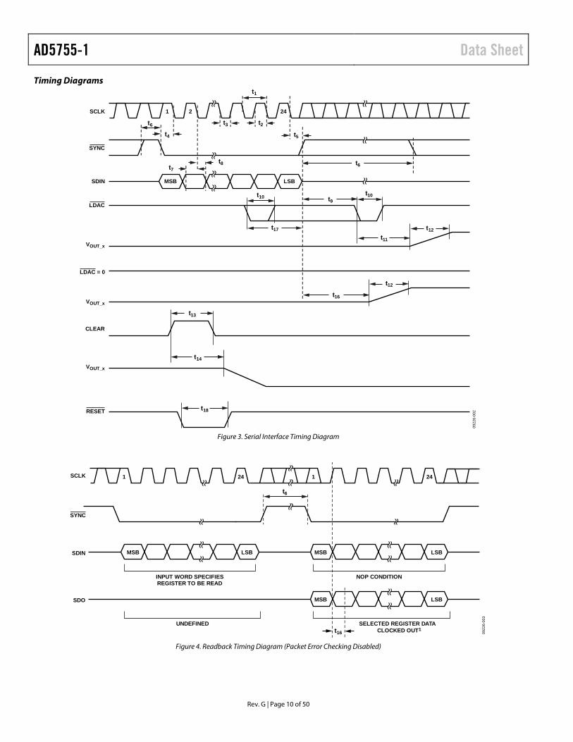
Timing Diagrams
0922
6-00
2
MSB
SCLK
SYNC
SDIN
LDAC
LDAC = 0
CLEAR
1 2 24
LSB
t1
VOUT_x
VOUT_x
VOUT_x
t4
t6 t3 t2
t5
t8t7
t10 t9t10
t11
t12
t12
t16
t17
t13
RESET t18
t14
t6
Figure 3. Serial Interface Timing Diagram
0922
6-00
3
SYNC
MSB MSBLSB LSB
INPUT WORD SPECIFIESREGISTER TO BE READ
NOP CONDITION
t6
t16
SDIN
MSB LSB
UNDEFINED SELECTED REGISTER DATACLOCKED OUT1
SDO
SCLK 24 241 1
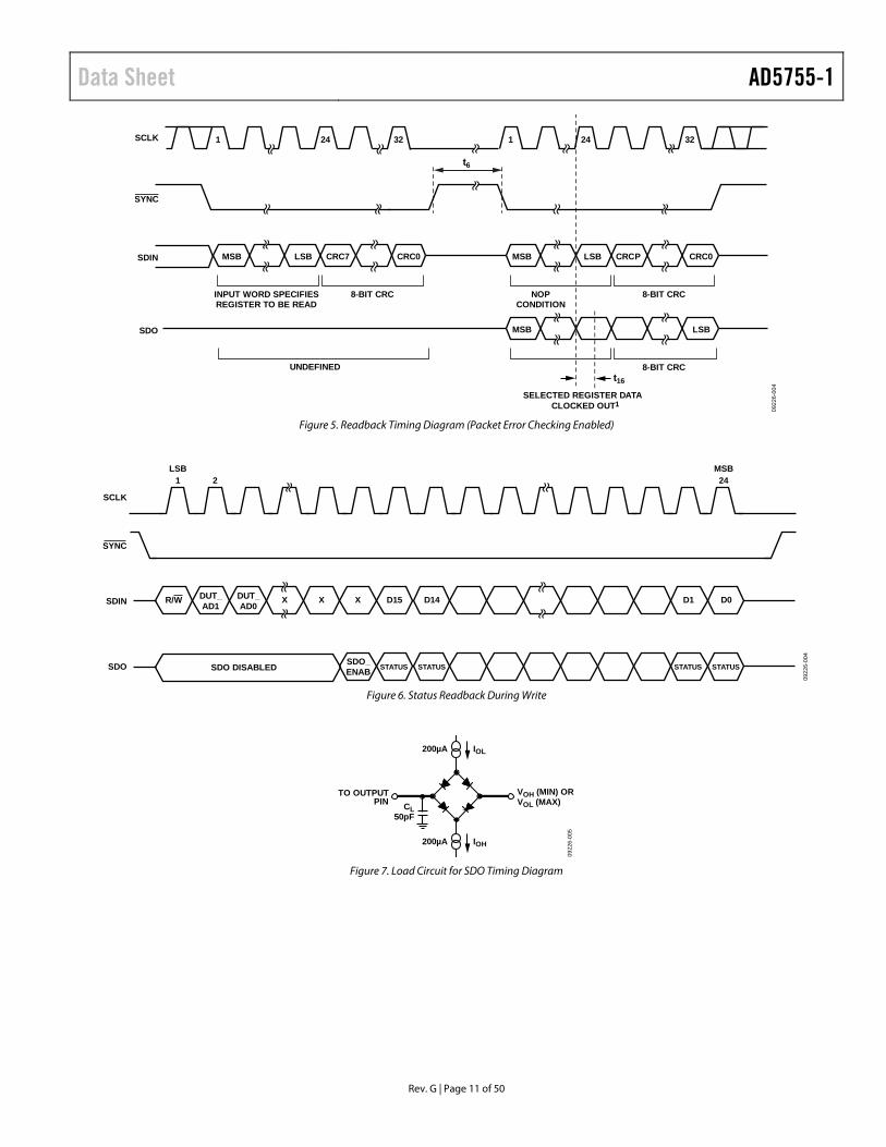
Figure 4. Readback Timing Diagram (Packet Error Checking Disabled)
Data Sheet AD5755-1
Rev. G | Page 11 of 50
0922
6-00
4
SYNC
MSB MSB LSBLSB CRCPCRC0CRC7 CRC0
INPUT WORD SPECIFIESREGISTER TO BE READ
8-BIT CRC NOPCONDITION
8-BIT CRC
8-BIT CRC
t6
t16
SDIN
MSB LSB
UNDEFINED
SELECTED REGISTER DATACLOCKED OUT1
SDO
SCLK 3224 32241 1
Figure 5. Readback Timing Diagram (Packet Error Checking Enabled)
SDO DISABLED
R/WSDIN
SCLK
SYNC
SDO
1 2 24LSB MSB
DUT_AD1
SDO_ENAB
DUT_AD0
X X X D15 D14 D1 D0
STATUSSTATUSSTATUSSTATUS
0922
6-00
4
Figure 6. Status Readback During Write
200µA IOL
200µA IOH
VOH (MIN) ORVOL (MAX)
TO OUTPUTPIN CL
50pF
0922
6-00
5
Figure 7. Load Circuit for SDO Timing Diagram
AD5755-1 Data Sheet
Rev. G | Page 12 of 50
ABSOLUTE MAXIMUM RATINGS TA = 25°C, unless otherwise noted. Transient currents of up to 100 mA do not cause SCR latch-up.
Table 4. Parameter Rating AVDD, VBOOST_x to AGND, DGND −0.3 V to +33 V AVSS to AGND, DGND +0.3 V to −28 V AVDD to AVSS −0.3 V to +60 V AVCC to AGND −0.3 V to +7 V DVDD to DGND −0.3 V to +7 V Digital Inputs to DGND −0.3 V to DVDD + 0.3 V or +7 V
(whichever is less) Digital Outputs to DGND −0.3 V to DVDD + 0.3 V or +7 V
(whichever is less) REFIN, REFOUT to AGND −0.3 V to AVDD + 0.3 V or +7 V
(whichever is less) VOUT_x to AGND AVSS to VBOOST_x or 33 V if using
the dc-to-dc circuitry +VSENSE_x to AGND AVSS to VBOOST_x or 33 V if using
the dc-to-dc circuitry IOUT_x to AGND AVSS to VBOOST_x or 33 V if using
the dc-to-dc circuitry SWx to AGND −0.3 to +33 V AGND, GNDSWx to DGND −0.3 V to +0.3 V Operating Temperature Range (TA)
Industrial1 −40°C to +105°C Storage Temperature Range −65°C to +150°C Junction Temperature (TJ max) 125°C 64-Lead LFCSP
θJA Thermal Impedance2 28°C/W Power Dissipation (TJ max − TA)/θJA Lead Temperature JEDEC industry standard
Soldering J-STD-020
1 Power dissipated on chip must be derated to keep the junction temperature below 125°C.
2 Based on a JEDEC 4-layer test board.
Stresses above those listed under Absolute Maximum Ratings may cause permanent damage to the device. This is a stress rating only; functional operation of the device at these or any other conditions above those indicated in the operational section of this specification is not implied. Exposure to absolute maximum rating conditions for extended periods may affect device reliability.
ESD CAUTION

Data Sheet AD5755-1
Rev. G | Page 13 of 50
PIN CONFIGURATION AND FUNCTION DESCRIPTIONS
17 18 19 20 21 22 23 24 25 26 27 28 29 30 31 32
POC
RES
ETAV
DD
CO
MP L
V_A
CH
AR
TA+V
SEN
SE_A
CO
MP D
CD
C_A
V BO
OST
_AV O
UT_
AI O
UT_
AAV
SSC
OM
P LV_
BC
HA
RTB
+VSE
NSE
_BV O
UT_
BC
OM
P DC
DC
_B
64 63 62 61 60 59 58 57 56 55 54 53 52 51 50 49
RSE
T_C
RSE
T_D
REF
OU
TR
EFIN
CO
MP L
V_D
CH
AR
TD+V
SEN
SE_D
CO
MP D
CD
C_D
V BO
OST
_DV O
UT_
DI O
UT_
DAV
SSC
OM
P LV_
CC
HA
RTC
+VSE
NSE
_CV O
UT_
C
123456789
10111213141516
RSET_BRSET_A
REFGNDREFGND
AD0AD1
SYNCSCLKSDINSDO
DVDDDGNDLDAC
CLEARALERTFAULT
COMPDCDC_CIOUT_CVBOOST_CAVCCSWCGNDSWCGNDSWDSWDAVSSSWAGNDSWAGNDSWBSWBAGNDVBOOST_BIOUT_B
48474645444342414039383736353433
AD5755-1TOP VIEW
(Not to Scale)
0926
6-00
6
PIN 1INDICATOR
NOTES1. THE EXPOSED PAD SHOULD BE CONNECTED TO THE POTENTIAL OF THE AVSS PIN, OR, ALTERNATIVELY, IT CAN BE LEFT ELECTRICALLY UNCONNECTED. IT IS RECOMMENDED THAT THE PAD BE THERMALLY CONNECTED TO A COPPER PLANE FOR ENHANCED THERMAL PERFORMANCE.
Figure 8. Pin Configuration
Table 5. Pin Function Descriptions Pin No. Mnemonic Description 1 RSET_B An external, precision, low drift 15 kΩ current setting resistor can be connected to this pin to improve the IOUT_B
temperature drift performance. See the Device Features section. 2 RSET_A An external, precision, low drift 15 kΩ current setting resistor can be connected to this pin to improve the IOUT_A
temperature drift performance. See the Device Features section. 3, 4 REFGND Ground Reference Point for Internal Reference. 5 AD0 Address Decode for the Device Under Test (DUT) on the Board. 6 AD1 Address Decode for the DUT on the Board. It is not recommended to tie both AD1 and AD0 low when using PEC,
see the Packet Error Checking section. 7 SYNC Active Low Input. This is the frame synchronization signal for the serial interface. While SYNC is low, data is
transferred in on the falling edge of SCLK. 8 SCLK Serial Clock Input. Data is clocked into the input shift register on the falling edge of SCLK. This operates at clock
speeds of up to 30 MHz. 9 SDIN Serial Data Input. Data must be valid on the falling edge of SCLK. 10 SDO Serial Data Output. Used to clock data from the serial register in readback mode. See Figure 4 and Figure 6. 11 DVDD Digital Supply. The voltage range is from 2.7 V to 5.5 V. 12 DGND Digital Ground. 13 LDAC Load DAC, Active Low Input. This is used to update the DAC register and consequently the DAC outputs. When
tied permanently low, the addressed DAC data register is updated on the rising edge of SYNC. If LDAC is held high during the write cycle, the DAC input register is updated, but the DAC output update only takes place at the falling edge of LDAC (see Figure 3). Using this mode, all analog outputs can be updated simultaneously. The LDAC pin must not be left unconnected.
14 CLEAR Active High, Edge Sensitive Input. Asserting this pin sets the output current and voltage to the preprogrammed clear code bit setting. Only channels enabled to be cleared are cleared. See the Device Features section for more
AD5755-1 Data Sheet
Rev. G | Page 14 of 50
Pin No. Mnemonic Description information. When CLEAR is active, the DAC output register cannot be written to.
15 ALERT Active High Output. This pin is asserted when there has been no SPI activity on the interface pins for a predetermined time. See the Device Features section for more information.
16 FAULT Active Low Output. This pin is asserted low when an open circuit in current mode is detected, a short circuit in voltage mode is detected, a PEC error is detected, or an overtemperature is detected (see the Device Features section). Open-drain output.
17 POC Power-On Condition. This pin determines the power-on condition and is read during power-on or, alternatively, after a device reset. If POC = 0, the device is powered up with the voltage and current channels in tristate mode. If POC = 1, the device is powered up with a 30 kΩ pull-down resistor to ground on the voltage output channel, and the current channel is in tristate mode.
18 RESET Hardware Reset, Active Low Input.
19 AVDD Positive Analog Supply. The voltage range is from 9 V to 33 V. 20 COMPLV_A Optional Compensation Capacitor Connection for VOUT_A Output Buffer. Connecting a 220 pF capacitor between
this pin and the VOUT_A pin allows the voltage output to drive up to 2 µF. Note that the addition of this capacitor reduces the bandwidth of the output amplifier, increasing the settling time.
21 CHARTA HART Input Connection for DAC Channel A. For more information, see the HART Connectivity section. If unused, leave as an open circuit.
22 +VSENSE_A Sense Connection for the Positive Voltage Output Load Connection for VOUT_A. 23 COMPDCDC_A DC-to-DC Compensation Capacitor. Connect a 10 nF capacitor from this pin to ground. Used to regulate the feedback
loop of the Channel A dc-to-dc converter. Alternatively, if using an external compensation resistor, place a resistor in series with a capacitor to ground from this pin (see the DC-to-DC Converter Compensation Capacitors and the AICC Supply Requirements—Slewing sections in the Device Features section for more information).
24 VBOOST_A Supply for Channel A Current Output Stage (see Figure 74). This is also the supply for the VOUT_x stage, which is regulated to 15 V by the dc-to-dc converter. To use the dc-to-dc feature of the device, connect as shown in Figure 81.
25 VOUT_A Buffered Analog Output Voltage for DAC Channel A. 26 IOUT_A Current Output Pin for DAC Channel A. 27 AVSS Negative Analog Supply. Voltage range is from 0 V to −26.4 V. 28 COMPLV_B Optional Compensation Capacitor Connection for VOUT_B Output Buffer. Connecting a 220 pF capacitor between
this pin and the VOUT_B pin allows the voltage output to drive up to 2 µF. Note that the addition of this capacitor reduces the bandwidth of the output amplifier, increasing the settling time.
29 CHARTB HART Input Connection for DAC Channel B. For more information, see the HART Connectivity section. If unused, leave as an open circuit.
30 +VSENSE_B Sense Connection for the Positive Voltage Output Load Connection for VOUT_B. 31 VOUT_B Buffered Analog Output Voltage for DAC Channel B. 32 COMPDCDC_B DC-to-DC Compensation Capacitor. Connect a 10 nF capacitor from this pin to ground. Used to regulate the feedback
loop of the Channel B dc-to-dc converter. Alternatively, if using an external compensation resistor, place a resistor in series with a capacitor to ground from this pin (see the DC-to-DC Converter Compensation Capacitors and AICC Supply Requirements—Slewing sections in the Device Features section for more information).
33 IOUT_B Current Output Pin for DAC Channel B. 34 VBOOST_B Supply for Channel B Current Output Stage (see Figure 74). This is also the supply for the VOUT_x stage, which is
regulated to 15 V by the dc-to-dc converter. To use the dc-to-dc feature of the device, connect as shown in Figure 81.
35 AGND Ground Reference Point for Analog Circuitry. This must be connected to 0 V. 36 SWB Switching Output for Channel B DC-to-DC Circuitry. To use the dc-to-dc feature of the device, connect as shown
in Figure 81. 37 GNDSWB Ground Connection for DC-to-DC Switching Circuit. This pin must always be connected to ground. 38 GNDSWA Ground Connection for DC-to-DC Switching Circuit. This pin must always be connected to ground. 39 SWA Switching Output for Channel A DC-to-DC Circuitry. To use the dc-to-dc feature of the device, connect as shown
in Figure 81. 40 AVSS Negative Analog Supply Pin. The voltage range is from −10.8 V to −26.4 V. This pin can be connected to 0 V if
using the device in unipolar supply mode. 41 SWD Switching Output for Channel D DC-DC Circuitry. To use the dc-to-dc feature of the device, connect as shown in
Figure 81.
Data Sheet AD5755-1
Rev. G | Page 15 of 50
Pin No. Mnemonic Description 42 GNDSWD Ground Connections for DC-to-DC Switching Circuit. This pin must always be connected to ground. 43 GNDSWC Ground Connections for DC-to-DC Switching Circuit. This pin must always be connected to ground. 44 SWC Switching Output for Channel C DC-to-DC Circuitry. To use the dc-to-dc feature of the device, connect as shown
in Figure 81. 45 AVCC Supply for DC-to-DC Circuitry. 46 VBOOST_C Supply for Channel C Current Output Stage (see Figure 74). This is also the supply for the VOUT_x stage, which is
regulated to 15 V by the dc-to-dc converter. To use the dc-to-dc feature of the device, connect as shown in Figure 81.
47 IOUT_C Current Output Pin for DAC Channel C. 48 COMPDCDC_C DC-to-DC Compensation Capacitor. Connect a 10 nF capacitor from this pin to ground. Used to regulate the
feedback loop of the Channel C dc-to-dc converter. Alternatively, if using an external compensation resistor, place a resistor in series with a capacitor to ground from this pin (see the DC-to-DC Converter Compensation Capacitors and AICC Supply Requirements—Slewing sections in the Device Features section for more information).
49 VOUT_C Buffered Analog Output Voltage for DAC Channel C. 50 +VSENSE_C Sense Connection for the Positive Voltage Output Load Connection for VOUT_C. 51 CHARTC HART Input Connection for DAC Channel C. For more information, see the HART Connectivity section. If unused,
leave as an open circuit. 52 COMPLV_C Optional Compensation Capacitor Connection for VOUT_C Output Buffer. Connecting a 220 pF capacitor between
this pin and the VOUT_C pin allows the voltage output to drive up to 2 µF. Note that the addition of this capacitor reduces the bandwidth of the output amplifier, increasing the settling time.
53 AVSS Negative Analog Supply Pin. 54 IOUT_D Current Output Pin for DAC Channel D. 55 VOUT_D Buffered Analog Output Voltage for DAC Channel D. 56 VBOOST_D Supply for Channel D Current Output Stage (see Figure 74). This is also the supply for the VOUT_x stage, which is
regulated to 15 V by the dc-to-dc converter. To use the dc-to-dc feature of the device, connect as shown in Figure 81.
57 COMPDCDC_D DC-to-DC Compensation Capacitor. Connect a 10 nF capacitor from this pin to ground. Used to regulate the feedback loop of the Channel D dc-to-dc converter. Alternatively, if using an external compensation resistor, place a resistor in series with a capacitor to ground from this pin (see the DC-to-DC Converter Compensation Capacitors and AICC Supply Requirements—Slewing sections in the Device Features section for more information).
58 +VSENSE_D Sense Connection for the Positive Voltage Output Load Connection for VOUT_D. 59 CHARTD HART Input Connection for DAC Channel D. For more information, see the HART Connectivity section. If unused,
leave as an open circuit. 60 COMPLV_D Optional Compensation Capacitor Connection for VOUT_D Output Buffer. Connecting a 220 pF capacitor between
this pin and the VOUT_D pin allows the voltage output to drive up to 2 µF. Note that the addition of this capacitor reduces the bandwidth of the output amplifier, increasing the settling time.
61 REFIN External Reference Voltage Input. 62 REFOUT Internal Reference Voltage Output. Place a 0.1 µF capacitor between REFOUT and REFGND.
REFOUT must be connected to REFIN to use the internal reference. 63 RSET_D An external, precision, low drift 15 kΩ current setting resistor can be connected to this pin to improve the IOUT_D
temperature drift performance. See the Device Features section. 64 RSET_C An external, precision, low drift 15 kΩ current setting resistor can be connected to this pin to improve the IOUT_C
temperature drift performance. See the Device Features section. EPAD Exposed Pad. Connect this exposed pad to the potential of the AVSS pin, or, alternatively, leave it electrically
unconnected. It is recommended that the pad be thermally connected to a copper plane for enhanced thermal performance.

AD5755-1 Data Sheet
Rev. G | Page 16 of 50
TYPICAL PERFORMANCE CHARACTERISTICS VOLTAGE OUTPUTS
0.0015
0.0010
0.0005
0
–0.0005
–0.00100 10k 20k 30k 40k 50k 60k
INL
ERR
OR
(%FS
R)
CODE 0922
6-02
3
±10V RANGE±5V RANGE+10V RANGE+5V RANGE+10V RANGE WITH DCDC
AVDD = +15VAVSS = –15VTA = 25°C
Figure 9. Integral Nonlinearity Error vs. DAC Code
–1.0
–0.8
–0.6
–0.4
–0.2
0
0.2
0.4
0.6
0.8
1.0
0 10k 20k 30k 40k 50k 60k
DN
L ER
RO
R (L
SB)
CODE
±10V RANGE±5V RANGE+10V RANGE+5V RANGE+10V RANGE WITH DCDC
AVDD = +15VAVSS = –15VTA = 25°C
0922
6-02
4
Figure 10. Differential Nonlinearity Error vs. DAC Code
10k 20k 30k 40k 50k 60k–0.010
–0.008
–0.006
–0.004
–0.002
0
0.002
0.004
0.006
0
TOTA
L U
NA
DJU
STED
ER
RO
R (%
FSR
)
CODE
±10V RANGE±5V RANGE+10V RANGE+5V RANGE+10V RANGE WITH DCDC
AVDD = +15VAVSS = –15VTA = 25°C
0922
6-02
5
Figure 11. Total Unadjusted Error vs. DAC Code
–0.0015
–0.0010
–0.0005
0
0.0005
0.0010
0.0015
–40 –20 0 20 40 60 80 100
INL
ERR
OR
(%FS
R)
TEMPERATURE (°C)
+5V RANGE MAX INL +10V RANGE MAX INL±5V RANGE MAX INL ±10V RANGE MAX INL+5V RANGE MIN INL +10V RANGE MIN INL±5V RANGE MIN INL ±10V RANGE MIN INL
AVDD = +15VAVSS = –15VOUTPUT UNLOADED
0922
6-12
7
Figure 12. Integral Nonlinearity Error vs. Temperature
–1.0
–0.8
–0.6
–0.4
–0.2
0
0.2
0.4
0.6
0.8
1.0
–40 –20 0 20 40 60 80 100
DN
L ER
RO
R (L
SB)
TEMPERATURE (°C)
AVDD = +15VAVSS = –15VALL RANGES
DNL ERROR MAXDNL ERROR MIN
0922
6-12
8
Figure 13. Differential Nonlinearity Error vs. Temperature
–0.006
–0.004
–0.002
0
0.002
0.004
0.006
0.008
0.010
0.012
–40 –20 0 20 40 60 80 100
TOTA
L U
NA
DJU
STED
ER
RO
R (%
FSR
)
TEMPERATURE (°C)
AVDD = +15VAVSS = –15VOUTPUT UNLOADED
+5V RANGE+10V RANGE±5V RANGE±10V RANGE
0922
6-12
9
Figure 14. Total Unadjusted Error vs. Temperature
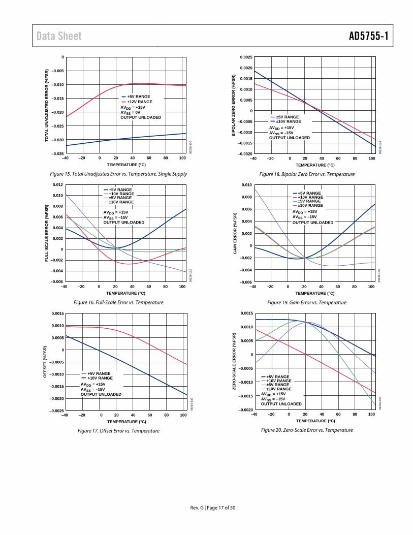
Data Sheet AD5755-1
Rev. G | Page 17 of 50
–0.035
–0.030
–0.025
–0.020
–0.015
–0.010
–0.005
0
–40 –20 0 20 40 60 80 100
TOTA
L U
NA
DJU
STED
ER
RO
R (%
FSR
)
TEMPERATURE (°C)
AVDD = +15VAVSS = 0VOUTPUT UNLOADED
+5V RANGE+12V RANGE
0922
6-13
0
Figure 15. Total Unadjusted Error vs. Temperature, Single Supply
–0.006
–0.004
–0.002
0
0.002
0.004
0.006
0.008
0.010
0.012
–40 –20 0 20 40 60 80 100
FULL
-SC
ALE
ER
RO
R (%
FSR
)
TEMPERATURE (°C)
AVDD = +15VAVSS = –15VOUTPUT UNLOADED
+5V RANGE+10V RANGE±5V RANGE±10V RANGE
0922
6-13
2
Figure 16. Full-Scale Error vs. Temperature
–0.0025
–0.0020
–0.0015
–0.0010
–0.0005
0
0.0005
0.0010
0.0015
–40 –20 0 20 40 60 80 100
OFF
SET
(%FS
R)
TEMPERATURE (°C)
AVDD = +15VAVSS = –15VOUTPUT UNLOADED
+5V RANGE+10V RANGE
0922
6-13
3
Figure 17. Offset Error vs. Temperature
–0.0020
–0.0015
–0.0010
–0.0005
0
0.0005
0.0010
0.0015
0.0020
0.0025
–40 –20 0 20 40 60 80 100
BIP
OLA
R Z
ERO
ER
RO
R (%
FSR
)
TEMPERATURE (°C)
AVDD = +15VAVSS = –15VOUTPUT UNLOADED
±5V RANGE±10V RANGE
0922
6-13
4
Figure 18. Bipolar Zero Error vs. Temperature
–0.006
–0.004
–0.002
0
0.002
0.004
0.006
0.008
0.010
–40 –20 0 20 40 60 80 100TEMPERATURE (°C)
AVDD = +15VAVSS = –15VOUTPUT UNLOADED
+5V RANGE+10V RANGE±5V RANGE±10V RANGE
GA
IN E
RR
OR
(%FS
R)
0922
6-13
5
Figure 19. Gain Error vs. Temperature
–0.0020
–0.0015
–0.0010
–0.0005
0
0.0005
0.0010
0.0015
ZER
O-S
CA
LE E
RR
OR
(%FS
R)
AVDD = +15VAVSS = –15VOUTPUT UNLOADED
+5V RANGE+10V RANGE±5V RANGE±10V RANGE
0922
6-13
6
–40 –20 0 20 40 60 80 100TEMPERATURE (°C)
Figure 20. Zero-Scale Error vs. Temperature

AD5755-1 Data Sheet
Rev. G | Page 18 of 50
0.0020
–0.002010 15 20 25 30
INL
ERR
OR
(%FS
R)
SUPPLY (V) 0922
6-03
4
–0.0015
–0.0010
–0.0005
0
0.0005
0.0010
0.0015
0V TO 10V RANGE MAX INL0V TO 10V RANGE MIN INLTA = 25°CAVSS = –26.4V FOR AVDD > +26.4V
Figure 21. Integral Nonlinearity Error vs. AVDD/|AVSS|
–1.0
–0.8
–0.6
–0.4
–0.2
0
0.2
0.4
0.6
0.8
1.0
10 15 20 25 30
DN
L ER
RO
R (L
SB)
SUPPLY (V)
AVSS = –26.4V FOR AVDD > +26.4V
AVDD = +15VAVSS = –15VALL RANGESTA = 25°C
DNL ERROR MAXDNL ERROR MIN
0922
6-13
8
Figure 22. Differential Nonlinearity Error vs. AVDD/|AVSS|
0.008
0.006
0.004
0.002
0
–0.008
–0.00410 15 20 25 30
TOTA
L U
NA
DJU
STED
ER
RO
R (%
FSR
)
SUPPLY (V) 0922
6-03
5
0V TO 10V RANGE MAX TUE0V TO 10V RANGE MIN TUETA = 25°CAVSS = –26.4V FOR AVDD > +26.4V
Figure 23. Total Unadjusted Error vs. AVDD/|AVSS|
0.0020
0.0015
0.0010
0.0005
0
–0.0005
–0.0010
–0.0015
–0.0020–20 201612840–4–8–12–16
OU
TPU
T VO
LTA
GE
DEL
TA (V
)
OUTPUT CURRENT (mA) 0922
6-03
6
8mA LIMIT, CODE = 0xFFFF16mA LIMIT, CODE = 0xFFFF
AVDD = +15VAVSS = –15V±10V RANGETA = 25°C
Figure 24. Source and Sink Capability of Output Amplifier
12
8
4
0
–4
–8
–12–5 151050
OU
TPU
T VO
LTA
GE
(V)
TIME (µs) 0922
6-03
7
AVDD = +15VAVSS = –15V±10V RANGETA = 25°COUTPUT UNLOADED
Figure 25. Full-Scale Positive Step
12
8
4
0
–4
–8
–12–5 151050
OU
TPU
T VO
LTA
GE
(V)
TIME (µs) 0922
6-03
8
AVDD = +15VAVSS = –15V±10V RANGETA = 25°COUTPUT UNLOADED
Figure 26. Full-Scale Negative Step
Data Sheet AD5755-1
Rev. G | Page 19 of 50
15
10
5
0
–5
–10
–15
–200 54321
OU
TPU
T VO
LTA
GE
(V)
TIME (µs) 0922
6-03
9
0x7FFF TO 0x80000x8000 TO 0x7FFF
THE EXTERNAL RESISTOR IS AVISHAY S102C, 0.6ppm RESISTOR
AVDD = +15VAVSS = –15V±10V RANGETA = 25°C
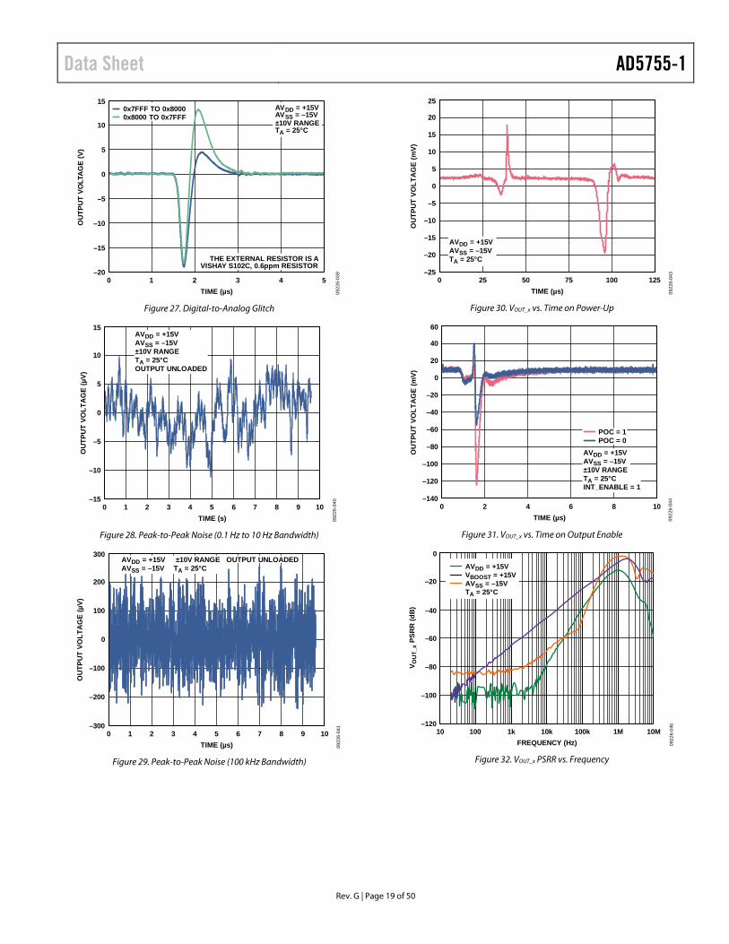
Figure 27. Digital-to-Analog Glitch
15
10
5
0
–5
–10
–150 7 8 9 105 61 2 3 4
OU
TPU
T VO
LTA
GE
(µV)
TIME (s) 0922
6-04
0AVDD = +15VAVSS = –15V±10V RANGETA = 25°COUTPUT UNLOADED
Figure 28. Peak-to-Peak Noise (0.1 Hz to 10 Hz Bandwidth)
300
200
100
0
–100
–200
–3000 7 8 9 105 61 2 3 4
OU
TPU
T VO
LTA
GE
(µV)
TIME (µs) 0922
6-04
1
AVDD = +15VAVSS = –15V
±10V RANGETA = 25°C
OUTPUT UNLOADED
Figure 29. Peak-to-Peak Noise (100 kHz Bandwidth)
25
20
15
10
5
0
–5
–10
–15
–20
–250 25 50 75 100 125
OU
TPU
T VO
LTA
GE
(mV)
TIME (µs) 0922
6-04
3
AVDD = +15VAVSS = –15VTA = 25°C
Figure 30. VOUT_x vs. Time on Power-Up
60
40
20
0
–20
–40
–60
–80
–100
–120
–1400 2 4 6 8 10
OU
TPU
T VO
LTA
GE
(mV)
TIME (µs) 0922
6-04
4
POC = 1POC = 0
AVDD = +15VAVSS = –15V±10V RANGETA = 25°CINT_ENABLE = 1
Figure 31. VOUT_x vs. Time on Output Enable
0
–120
–100
–80
–60
–40
–20
10 100 1k 10k 100k 1M 10M
VO
UT_
x PS
RR
(dB
)
FREQUENCY (Hz) 0922
6-04
5
AVDD = +15VVBOOST = +15VAVSS = –15VTA = 25°C
Figure 32. VOUT_x PSRR vs. Frequency

AD5755-1 Data Sheet
Rev. G | Page 20 of 50
CURRENT OUTPUTS
–0.0025
–0.0015
–0.0005
0.0005
0.0015
0.0025
0 10000 20000 30000 40000 50000 60000
INL
ERR
OR
(%FS
R)
CODE
AVDD = +15VAVSS = –15VTA = 25°C
4mA TO 20mA, EXTERNAL RSET4mA TO 20mA, EXTERNAL RSET, WITH DC-TO-DC CONVERTER4mA TO 20mA, INTERNAL RSET4mA TO 20mA, INTERNAL RSET, WITH DC-TO-DC CONVERTER
0922
6-14
9
Figure 33. Integral Nonlinearity vs. Code
0 10000 20000 30000 40000 50000 60000
DN
L ER
RO
R (L
SB)
CODE
AVDD = +15VAVSS = –15VTA = 25°C
0922
6-15
0
–1.0
–0.8
–0.6
–0.4
–0.2
0
0.2
0.4
0.6
0.8
1.0
4mA TO 20mA, EXTERNAL RSET4mA TO 20mA, EXTERNAL RSET, WITH DC-TO-DC CONVERTER4mA TO 20mA, INTERNAL RSET4mA TO 20mA, INTERNAL RSET, WITH DC-TO-DC CONVERTER
Figure 34. Differential Nonlinearity vs. Code
0 10000 20000 30000 40000 50000 60000
TOTA
L U
NA
DJU
STED
ER
RO
R (%
FSR
)
CODE
0922
6-15
1
–0.015
–0.010
–0.005
0
0.005
0.010
0.015
0.020
0.025
0.030
0.035
AVDD = +15VAVSS = –15VTA = 25°CALL CHANNELS ENABLED
4mA TO 20mA, EXTERNAL RSET4mA TO 20mA, EXTERNAL RSET, WITH DC-TO-DC CONVERTER4mA TO 20mA, INTERNAL RSET4mA TO 20mA, INTERNAL RSET, WITH DC-TO-DC CONVERTER
Figure 35. Total Unadjusted Error vs. Code
–0.0010
–0.0008
–0.0006
–0.0004
–0.0002
0
0.0002
0.0004
0.0006
0.0008
0.0010
INL
ERR
OR
(%FS
R)
4mA TO 20mA RANGE MAX INL
0mA TO 20mA RANGE MAX INL
0mA TO 24mA RANGE MAX INL
4mA TO 20mA RANGE MAX INL0mA TO 24mA RANGE MIN INL
0mA TO 20mA RANGE MIN INL
AVDD = +15VAVSS = –15V/0V
–40 –20 0 20 40 60 80 100TEMPERATURE (°C)
0922
6-15
2
Figure 36. Integral Nonlinearity vs. Temperature, Internal RSET
–0.0020
–0.0015
–0.0010
–0.0005
0
0.0005
0.0010
0.0015
0.0020
INL
ERR
OR
(%FS
R)
4mA TO 20mA RANGE MAX INL
0mA TO 20mA RANGE MAX INL
0mA TO 24mA RANGE MAX INL
4mA TO 20mA RANGE MIN INL0mA TO 24mA RANGE MIN INL
0mA TO 20mA RANGE MIN INL
–40 –20 0 20 40 60 80 100TEMPERATURE (°C)
AVDD = +15VAVSS = –15V/0V
0922
6-15
3
Figure 37. Integral Nonlinearity vs. Temperature, External RSET
–1.0
–0.8
–0.6
–0.4
–0.2
0
0.2
0.4
0.6
0.8
1.0
–40 –20 0 20 40 60 80 100
DN
L ER
RO
R (L
SB)
TEMPERATURE (°C)
AVDD = +15VAVSS = –15V/0VALL RANGESINTERNAL AND EXTERNAL RSET
DNL ERROR MAXDNL ERROR MIN
0922
6-15
4
Figure 38. Differential Nonlinearity vs. Temperature
Data Sheet AD5755-1
Rev. G | Page 21 of 50
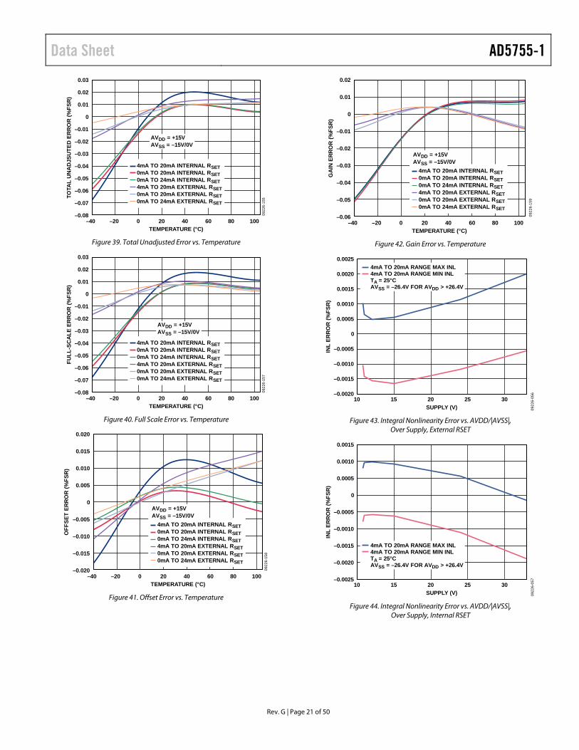
–0.08
–0.07
–0.06
–0.05
–0.04
–0.03
–0.02
–0.01
0
0.01
0.02
0.03
TOTA
L U
NA
DJS
UTE
D E
RR
OR
(%FS
R)
–40 –20 0 20 40 60 80 100TEMPERATURE (°C)
AVDD = +15VAVSS = –15V/0V
4mA TO 20mA INTERNAL RSET
4mA TO 20mA EXTERNAL RSET
0mA TO 20mA INTERNAL RSET
0mA TO 20mA EXTERNAL RSET0mA TO 24mA EXTERNAL RSET
0mA TO 24mA INTERNAL RSET
0922
6-15
5
Figure 39. Total Unadjusted Error vs. Temperature
–0.08
–0.07
–0.06
–0.05
–0.04
–0.03
–0.02
–0.01
0
0.01
0.02
0.03
FULL
-SC
ALE
ER
RO
R (%
FSR
)
–40 –20 0 20 40 60 80 100TEMPERATURE (°C)
AVDD = +15VAVSS = –15V/0V
4mA TO 20mA INTERNAL RSET
4mA TO 20mA EXTERNAL RSET
0mA TO 20mA INTERNAL RSET
0mA TO 20mA EXTERNAL RSET0mA TO 24mA EXTERNAL RSET
0mA TO 24mA INTERNAL RSET
0922
6-15
7
Figure 40. Full Scale Error vs. Temperature
–0.020
–0.015
–0.010
–0.005
0
0.005
0.010
0.015
0.020
OFF
SET
ERR
OR
(%FS
R)
–40 –20 0 20 40 60 80 100TEMPERATURE (°C)
4mA TO 20mA INTERNAL RSET
4mA TO 20mA EXTERNAL RSET
0mA TO 20mA INTERNAL RSET
0mA TO 20mA EXTERNAL RSET0mA TO 24mA EXTERNAL RSET
0mA TO 24mA INTERNAL RSET
AVDD = +15VAVSS = –15V/0V
0922
6-15
8
Figure 41. Offset Error vs. Temperature
–0.06
–0.05
–0.04
–0.03
–0.02
–0.01
0
0.01
0.02
GA
IN E
RR
OR
(%FS
R)
–40 –20 0 20 40 60 80 100TEMPERATURE (°C)
4mA TO 20mA INTERNAL RSET
4mA TO 20mA EXTERNAL RSET
0mA TO 20mA INTERNAL RSET
0mA TO 20mA EXTERNAL RSET0mA TO 24mA EXTERNAL RSET
0mA TO 24mA INTERNAL RSET
AVDD = +15VAVSS = –15V/0V
0922
6-15
9
Figure 42. Gain Error vs. Temperature
–0.0020
–0.0015
–0.0010
–0.0005
0
0.0005
0.0010
0.0015
0.0020
0.0025
10 15 20 25 30
INL
ERR
OR
(%FS
R)
SUPPLY (V)
4mA TO 20mA RANGE MAX INL4mA TO 20mA RANGE MIN INLTA = 25°CAVSS = –26.4V FOR AVDD > +26.4V
0922
6-05
6
Figure 43. Integral Nonlinearity Error vs. AVDD/|AVSS|,
Over Supply, External RSET
–0.0020
–0.0025
–0.0015
–0.0010
–0.0005
0
0.0005
0.0010
0.0015
10 15 20 25 30
INL
ERR
OR
(%FS
R)
SUPPLY (V)
4mA TO 20mA RANGE MAX INL4mA TO 20mA RANGE MIN INLTA = 25°CAVSS = –26.4V FOR AVDD > +26.4V
0922
6-05
7
Figure 44. Integral Nonlinearity Error vs. AVDD/|AVSS|,
Over Supply, Internal RSET
AD5755-1 Data Sheet
Rev. G | Page 22 of 50
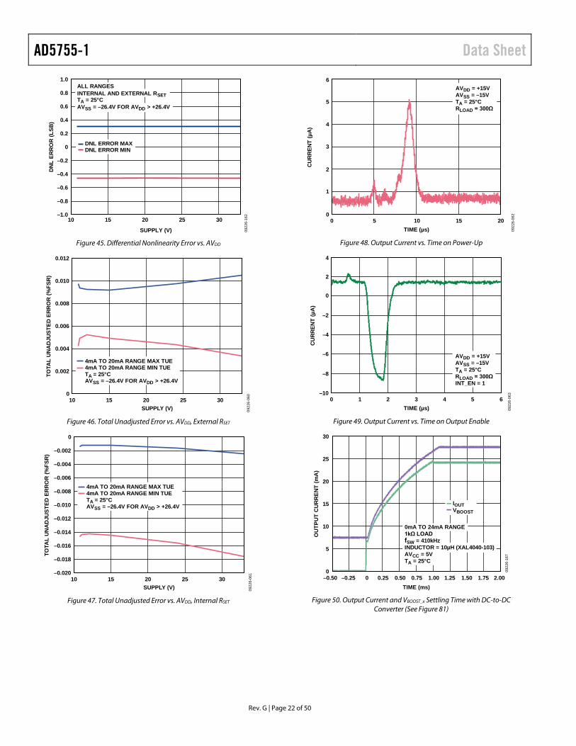
–1.0
–0.8
–0.6
–0.4
–0.2
0
0.2
0.4
0.6
0.8
1.0
10 15 20 25 30
DN
L ER
RO
R (L
SB)
SUPPLY (V)
DNL ERROR MAXDNL ERROR MIN
0922
6-16
2
AVSS = –26.4V FOR AVDD > +26.4V
ALL RANGESINTERNAL AND EXTERNAL RSETTA = 25°C
Figure 45. Differential Nonlinearity Error vs. AVDD
0
0.002
0.004
0.006
0.008
0.010
0.012
10 15 20 25 30
TOTA
L U
NA
DJU
STED
ER
RO
R (%
FSR
)
SUPPLY (V)
4mA TO 20mA RANGE MAX TUE4mA TO 20mA RANGE MIN TUETA = 25°CAVSS = –26.4V FOR AVDD > +26.4V
0922
6-06
0
Figure 46. Total Unadjusted Error vs. AVDD, External RSET
10 15 20 25 30
TOTA
L U
NA
DJU
STED
ER
RO
R (%
FSR
)
SUPPLY (V)
4mA TO 20mA RANGE MAX TUE4mA TO 20mA RANGE MIN TUETA = 25°CAVSS = –26.4V FOR AVDD > +26.4V
–0.020
–0.018
–0.016
–0.014
–0.012
–0.010
–0.008
–0.006
–0.004
–0.002
0
0922
6-06
1
Figure 47. Total Unadjusted Error vs. AVDD, Internal RSET
6
5
4
3
2
1
00 2015105
CU
RR
ENT
(µA
)
TIME (µs) 0922
6-06
2
AVDD = +15VAVSS = –15VTA = 25°CRLOAD = 300Ω
Figure 48. Output Current vs. Time on Power-Up
4
–10
–8
–6
–4
–2
0
2
0 1 2 3 4 5 6
CU
RR
ENT
(µA
)
TIME (µs) 0922
6-06
3
AVDD = +15VAVSS = –15VTA = 25°CRLOAD = 300ΩINT_EN = 1
Figure 49. Output Current vs. Time on Output Enable
0
5
10
15
20
25
30
OU
TPU
T C
UR
REN
T (m
A)
–0.50 –0.25 0 0.25 0.50 0.75 1.00 1.25 1.50 1.75 2.00TIME (ms)
0mA TO 24mA RANGE1kΩ LOADfSW = 410kHzINDUCTOR = 10µH (XAL4040-103)AVCC = 5VTA = 25°C
0922
6-16
7IOUTVBOOST
Figure 50. Output Current and VBOOST_x Settling Time with DC-to-DC
Converter (See Figure 81)
Data Sheet AD5755-1
Rev. G | Page 23 of 50
0
5
10
15
20
25
30
OU
TPU
T C
UR
REN
T (m
A)
–0.25 0 0.25 0.50 0.75 1.00 1.25 1.50 1.75TIME (ms)
0922
6-16
8
IOUT, TA = –40°CIOUT, TA = +25°CIOUT, TA = +105°C
0mA TO 24mA RANGE1kΩ LOADfSW = 410kHzINDUCTOR = 10µH (XAL4040-103)AVCC = 5V
Figure 51. Output Current Settling with DC-to-DC Converter vs. Time and
Temperature (See Figure 81)
0
5
10
15
20
25
30
OU
TPU
T C
UR
REN
T (m
A)
–0.25 0 0.25 0.50 0.75 1.00 1.25 1.50 1.75TIME (ms)
0922
6-16
9
IOUT, AVCC = 4.5VIOUT, AVCC = 5.0VIOUT, AVCC = 5.5V
0mA TO 24mA RANGE1kΩ LOADfSW = 410kHzINDUCTOR = 10µH (XAL4040-103)TA = 25°C
Figure 52. Output Current Settling with DC-to-DC Converter vs. Time and
AVCC (See Figure 81)
–10
–8
–6
–4
–2
0
2
4
6
8
10
0 2 4 6 8 10 12 14
CU
RR
ENT
(AC
-CO
UPL
ED) (
µA)
TIME (µs)
AVDD = 5VfSW = 410kHzINDUCTOR = 10µH (XAL4040-103)
0mA TO 24mA RANGE1kΩ LOAD
EXTERNAL RSETTA = 25°C
20mA OUTPUT10mA OUTPUT
0922
6-17
0
Figure 53. Output Current vs. Time with DC-to-DC Converter (See Figure 81)
8
7
6
5
4
3
2
1
00 5 10 15 20
HEA
DR
OO
M V
OLT
AG
E (V
)
CURRENT (mA) 0922
6-06
7
0mA TO 24mA RANGE1kΩ LOADFSW = 410kHzINDUCTOR = 10µH (XAL4040-103)TA = 25°C
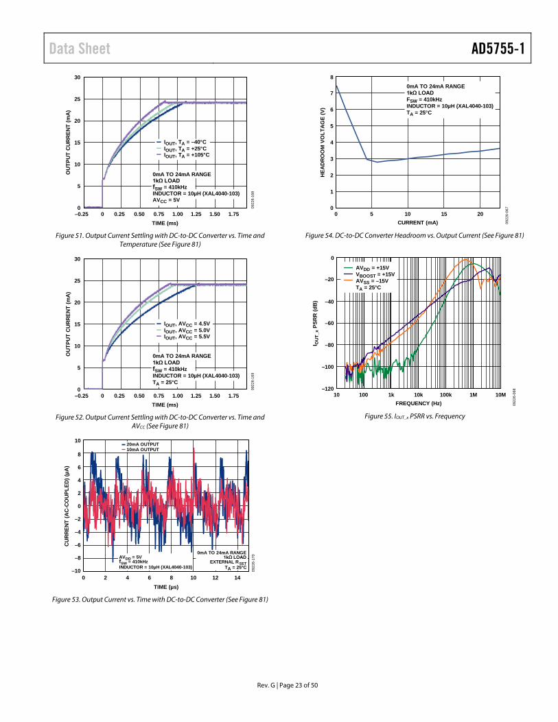
Figure 54. DC-to-DC Converter Headroom vs. Output Current (See Figure 81)
0
–120
–100
–80
–60
–40
–20
10 100 1k 10k 100k 1M 10M
I OU
T_x
PSR
R (d
B)
FREQUENCY (Hz) 0922
6-06
8
AVDD = +15VVBOOST = +15VAVSS = –15VTA = 25°C
Figure 55. IOUT_x PSRR vs. Frequency
AD5755-1 Data Sheet
Rev. G | Page 24 of 50
DC-TO-DC BLOCK
0
10
20
30
40
50
60
70
80
90
100
0 0.005 0.010 0.015 0.020 0.025
V BO
OST
EFF
ICIE
NCY
(%)
OUTPUT CURRENT (A)
AVDD = 4.5VAVDD = 5.0VAVDD = 5.5V
0922
6-25
5
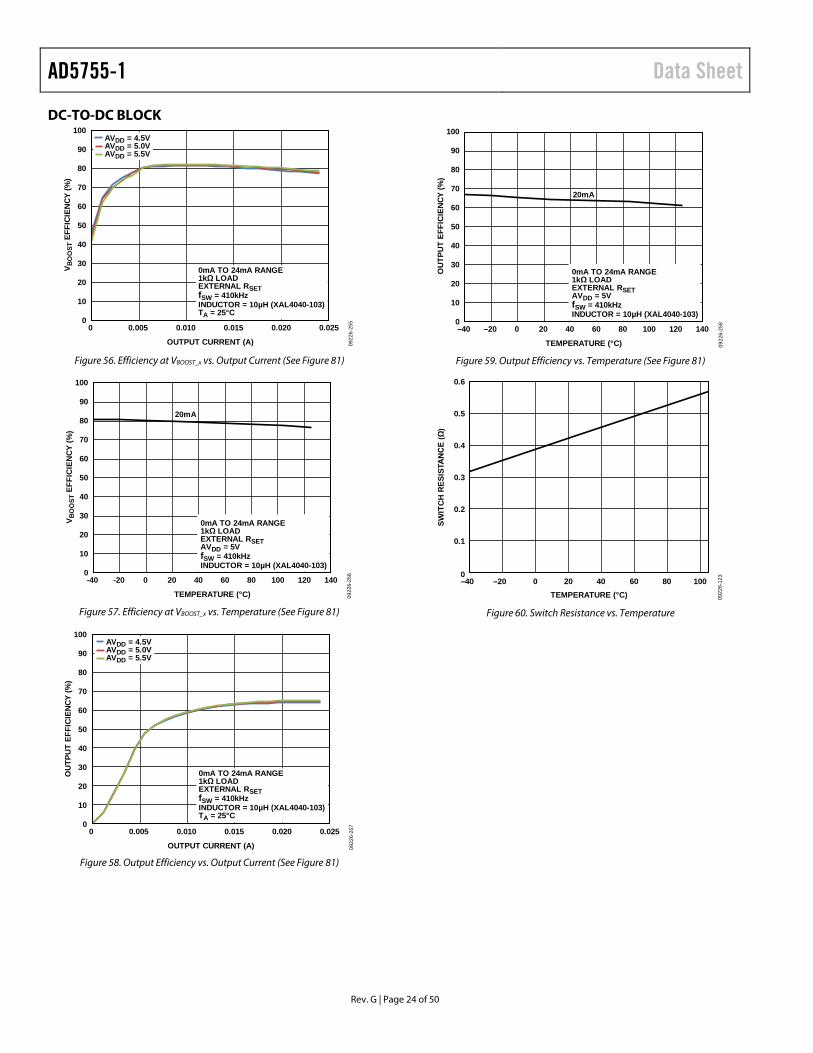
0mA TO 24mA RANGE1kΩ LOADEXTERNAL RSETfSW = 410kHzINDUCTOR = 10µH (XAL4040-103)TA = 25°C
Figure 56. Efficiency at VBOOST_x vs. Output Current (See Figure 81)
0
10
20
30
40
50
60
70
80
90
100
-40 -20 0 20 40 60 80 100 120 140
V BO
OST
EFF
ICIE
NCY
(%)
TEMPERATURE (°C)
20mA
0922
6-2 5
6
0mA TO 24mA RANGE1kΩ LOADEXTERNAL RSETAVDD = 5VfSW = 410kHzINDUCTOR = 10µH (XAL4040-103)
Figure 57. Efficiency at VBOOST_x vs. Temperature (See Figure 81)
0
10
20
30
40
50
60
70
80
90
100
0 0.005 0.010 0.015 0.020 0.025
OU
TPU
T EF
FIC
IEN
CY (%
)
OUTPUT CURRENT (A)
AVDD = 4.5VAVDD = 5.0VAVDD = 5.5V
0922
6-25
7
0mA TO 24mA RANGE1kΩ LOADEXTERNAL RSETfSW = 410kHzINDUCTOR = 10µH (XAL4040-103)TA = 25°C
Figure 58. Output Efficiency vs. Output Current (See Figure 81)
0
10
20
30
40
50
60
70
80
90
100
–40 –20 0 20 40 60 80 100 120 140
OU
TPU
T EF
FIC
IEN
CY (%
)
TEMPERATURE (°C)
20mA
0922
6-25
8
0mA TO 24mA RANGE1kΩ LOADEXTERNAL RSETAVDD = 5VfSW = 410kHzINDUCTOR = 10µH (XAL4040-103)
Figure 59. Output Efficiency vs. Temperature (See Figure 81)
0
0.1
0.2
0.3
0.4
0.5
0.6
–40 –20 0 20 40 60 80 100
SWIT
CH
RES
ISTA
NC
E (Ω
)
TEMPERATURE (°C) 0922
6-12
3
Figure 60. Switch Resistance vs. Temperature
Data Sheet AD5755-1
Rev. G | Page 25 of 50
REFERENCE 16
14
12
10
8
6
4
2
0
–20 0.2 0.4 0.6 0.8 1.0 1.2
VOLT
AG
E (V
)
TIME (ms) 0922
6-01
0
AVDDREFOUTTA = 25°C
Figure 61. REFOUT Turn-On Transient
4
3
2
1
0
–1
–2
–30 2 4 6 8 10
REF
EREN
CE
OU
TPU
T VO
LTA
GE
(µV)
TIME (s) 0922
6-01
1
AVDD = 15VTA = 25°C
Figure 62. REFOUT Output Noise (0.1 Hz to 10 Hz Bandwidth)
150
100
50
0
–50
–100
–1500 5 10 15 20
REF
EREN
CE
OU
TPU
T VO
LTA
GE
(µV)
TIME (ms) 0922
6-01
2
AVDD = 15VTA = 25°C
Figure 63. REFOUT Output Noise (100 kHz Bandwidth)
5.0000
5.0005
5.0010
5.0015
5.0020
5.0025
5.0030
5.0035
5.0040
5.0045
5.0050
–40 –20 0 20 40 60 80 100
REF
OU
T (V
)
TEMPERATURE (°C)
30 DEVICES SHOWNAVDD = 15V
0922
6-16
3
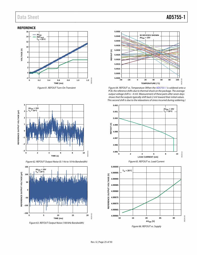
Figure 64. REFOUT vs. Temperature (When the AD5755-1 is soldered onto a PCB, the reference shifts due to thermal shock on the package. The average output voltage shift is −4 mV. Measurement of these parts after seven days shows that the outputs typically shift back 2 mV toward their initial values.
This second shift is due to the relaxations of stress incurred during soldering.)
5.002
5.001
5.000
4.999
4.998
4.997
4.996
4.9950 2 4 6 8 10
REF
OU
T (V
)
LOAD CURRENT (mA) 0922
6-01
4
AVDD = 15VTA = 25°C
Figure 65. REFOUT vs. Load Current
5.00000
4.99995
4.99990
4.99980
4.99985
4.99975
4.99970
4.99965
4.9996010 15 20 25 30
REF
EREN
CE
OU
TPU
T VO
LTA
GE
(V)
AVDD (V) 0922
6-01
5
TA = 25°C
Figure 66. REFOUT vs. Supply
AD5755-1 Data Sheet
Rev. G | Page 26 of 50
GENERAL 450
400
350
300
250
200
150
100
50
00 1 2 3 4 5
DI C
C (µ
A)
SDIN VOLTAGE (V) 0922
6-00
7
DVDD = 5VTA = 25°C
Figure 67. DICC vs. Logic Input Voltage
10
8
6
4
2
0
–12
–10
–8
–6
–4
–2
10 15 20 25 30
CU
RR
ENT
(mA
)
VOLTAGE (V) 0922
6-00
8
AIDDAISSTA = 25°CVOUT = 0VOUTPUT UNLOADED
Figure 68. AIDD/AISS vs. AVDD/|AVSS|
8
7
0
1
2
3
4
5
6
CU
RR
ENT
(mA
)
VOLTAGE (V) 0922
6-00
9
AIDDTA = 25°CIOUT = 0mA
10 15 20 25 30
Figure 69. AIDD vs. AVDD
13.4
13.3
13.2
13.1
13.0
12.9
12.8
12.7
12.6–40 –20 0 20 40 60 80 100
FREQ
UEN
CY
(MH
z)
TEMPERATURE (°C) 0922
6-02
0
DVDD = 5.5V
Figure 70. Internal Oscillator Frequency vs. Temperature
14.4
14.2
14.0
13.8
13.6
13.4
13.2
13.02.5 3.0 3.5 4.0 4.5 5.0 5.5
FREQ
UEN
CY
(MH
z)
VOLTAGE (V) 0922
6-02
1
DVDD = 5.5VTA = 25°C
Figure 71. Internal Oscillator Frequency vs. DVDD Supply Voltage

Data Sheet AD5755-1
Rev. G | Page 27 of 50
TERMINOLOGY Relative Accuracy or Integral Nonlinearity (INL) For the DAC, relative accuracy, or integral nonlinearity, is a measure of the maximum deviation, in LSBs, from the best fit line through the DAC transfer function. A typical INL vs. code plot is shown in Figure 9.
Differential Nonlinearity (DNL) Differential nonlinearity (DNL) is the difference between the measured change and the ideal 1 LSB change between any two adjacent codes. A specified differential nonlinearity of ±1 LSB maximum ensures monotonicity. This DAC is guaranteed mono-tonic by design. A typical DNL vs. code plot is shown in Figure 10.
Monotonicity A DAC is monotonic if the output either increases or remains constant for increasing digital input code. The AD5755-1 is monotonic over its full operating temperature range.
Negative Full-Scale Error/Zero-Scale Error Negative full-scale error is the error in the DAC output voltage when 0x0000 (straight binary coding) is loaded to the DAC register.
Zero-Scale TC This is a measure of the change in zero-scale error with a change in temperature. Zero-scale error TC is expressed in ppm FSR/°C.
Bipolar Zero Error Bipolar zero error is the deviation of the analog output from the ideal half-scale output of 0 V when the DAC register is loaded with 0x8000 (straight binary coding).
Bipolar Zero TC Bipolar zero TC is a measure of the change in the bipolar zero error with a change in temperature. It is expressed in ppm FSR/°C.
Offset Error In voltage output mode, offset error is the deviation of the analog output from the ideal quarter-scale output when in bipolar output ranges and the DAC register is loaded with 0x4000 (straight binary coding).
In current output mode, offset error is the deviation of the analog output from the ideal zero-scale output when all DAC registers are loaded with 0x0000.
Gain Error This is a measure of the span error of the DAC. It is the devia-tion in slope of the DAC transfer characteristic from the ideal, expressed in % FSR.
Gain TC This is a measure of the change in gain error with changes in temperature. Gain TC is expressed in ppm FSR/°C.
Full-Scale Error Full-scale error is a measure of the output error when full-scale code is loaded to the DAC register. Ideally, the output is full-
scale − 1 LSB. Full-scale error is expressed in percent of full-scale range (% FSR).
Full-Scale TC Full-scale TC is a measure of the change in full-scale error with changes in temperature and is expressed in ppm FSR/°C.
Total Unadjusted Error Total unadjusted error (TUE) is a measure of the output error taking all the various errors into account, including INL error, offset error, gain error, temperature, and time. TUE is expressed in % FSR.
DC Crosstalk This is the dc change in the output level of one DAC in response to a change in the output of another DAC. It is measured with a full-scale output change on one DAC while monitoring another DAC, which is at midscale.
Current Loop Compliance Voltage The maximum voltage at the IOUT_x pin for which the output current is equal to the programmed value.
Voltage Reference Thermal Hysteresis Voltage reference thermal hysteresis is the difference in output voltage measured at +25°C compared to the output voltage measured at +25°C after cycling the temperature from +25°C to −40°C to +105°C and back to +25°C. The hysteresis is expressed in ppm.
Output Voltage Settling Time Output voltage settling time is the amount of time it takes for the output to settle to a specified level for a full-scale input change. A plot of settling time is shown in Figure 25, Figure 51, and Figure 52.
Slew Rate The slew rate of a device is a limitation in the rate of change of the output voltage. The output slewing speed of a voltage-output digital-to-analog converter is usually limited by the slew rate of the amplifier used at its output. Slew rate is measured from 10% to 90% of the output signal and is given in V/µs.
Power-On Glitch Energy Power-on glitch energy is the impulse injected into the analog output when the AD5755-1 is powered-on. It is specified as the area of the glitch in nV-sec. See Figure 30 and Figure 48.
Digital-to-Analog Glitch Impulse Digital-to-analog glitch impulse is the impulse injected into the analog output when the input code in the DAC register changes state, but the output voltage remains constant. It is normally specified as the area of the glitch in nV-sec and is measured when the digital input code is changed by 1 LSB at the major carry transition (~0x7FFF to 0x8000). See Figure 27.
AD5755-1 Data Sheet
Rev. G | Page 28 of 50
Glitch Impulse Peak Amplitude Glitch impulse peak amplitude is the peak amplitude of the impulse injected into the analog output when the input code in the DAC register changes state. It is specified as the amplitude of the glitch in mV and is measured when the digital input code is changed by 1 LSB at the major carry transition (~0x7FFF to 0x8000). See Figure 27.
Digital Feedthrough Digital feedthrough is a measure of the impulse injected into the analog output of the DAC from the digital inputs of the DAC but is measured when the DAC output is not updated. It is specified in nV-sec and measured with a full-scale code change on the data bus.
DAC-to-DAC Crosstalk DAC-to-DAC crosstalk is the glitch impulse transferred to the output of one DAC due to a digital code change and a subsequent output change of another DAC. This includes both digital and analog crosstalk. It is measured by loading one of the DACs with a full-scale code change (all 0s to all 1s and vice versa) with LDAC low and monitoring the output of another DAC. The energy of the glitch is expressed in nV-sec.
Power Supply Rejection Ratio (PSRR) PSRR indicates how the output of the DAC is affected by changes in the power supply voltage.
Reference TC Reference TC is a measure of the change in the reference output voltage with a change in temperature. It is expressed in ppm/°C.
Line Regulation Line regulation is the change in reference output voltage due to a specified change in supply voltage. It is expressed in ppm/V.
Load Regulation Load regulation is the change in reference output voltage due to a specified change in load current. It is expressed in ppm/mA.
DC-to-DC Converter Headroom This is the difference between the voltage required at the current output and the voltage supplied by the dc-to-dc converter. See Figure 54.
Output Efficiency
CCCC
LOAD
AIAV
RIOUT
×
×2
This is defined as the power delivered to a channel’s load vs. the power delivered to the channel’s dc-to-dc input.
Efficiency at VBOOST_x
CCCC
xBOOSTOUT
AIAVVI×
× _
This is defined as the power delivered to a channel’s VBOOST_x supply vs. the power delivered to the dc-to-dc input of the channel. The VBOOST_x quiescent current is considered part of the dc-to-dc converter’s losses.

Data Sheet AD5755-1
Rev. G | Page 29 of 50
THEORY OF OPERATION The AD5755-1 is a quad, precision digital-to-current loop and voltage output converter designed to meet the requirements of industrial process control applications. It provides a high precision, fully integrated, low cost, single-chip solution for generating current loop and unipolar/bipolar voltage outputs. The current ranges available are 0 mA to 20 mA, 0 mA to 24 mA, and 4 mA to 20 mA. The voltage ranges available are 0 V to 5 V, ±5 V, 0 V to 10 V, and ±10 V. The current and voltage outputs are availa-ble on separate pins, and only one is active at any one time. The desired output configuration is user selectable via the DAC control register.
On-chip dynamic power control minimizes package power dissipation in current mode.
DAC ARCHITECTURE The DAC core architecture of the AD5755-1 consists of two matched DAC sections. A simplified circuit diagram is shown in Figure 72. The four MSBs of the 16-bit data-word are decoded to drive 15 switches, E1 to E15. Each of these switches connects one of 15 matched resistors to either ground or the reference buffer output. The remaining 12 bits of the data-word drive Switch S0 to Switch S11 of a 12-bit voltage mode R-2R ladder network.
12-BIT R-2R LADDER FOUR MSBs DECODED INTO15 EQUAL SEGMENTS
2R 2R
S0 S1 S7/S11 E1 E2 E15
VOUT
2R 2R 2R 2R 2R
0922
6-06
9
Figure 72. DAC Ladder Structure
The voltage output from the DAC core is either converted to a current (see Figure 74), which is then mirrored to the supply rail so that the application simply sees a current source output, or it is buffered and scaled to output a software selectable unipolar or bipolar voltage range (see Figure 73). Both the voltage and current outputs are supplied by VBOOST_x. The current and voltage are output on separate pins and cannot be output simultaneously. A channel’s current and voltage output pins can be tied together.
0922
6-07
0
RANGESCALINGDAC
VOUT_X SHORT FAULT
+VSENSE_x
VOUT_x
Figure 73. Voltage Output
0922
6-07
1
16-BITDAC
VBOOST_x
R2
T2
T1
R3
IOUT_x
RSET
A1
A2
Figure 74. Voltage-to-Current Conversion Circuitry
Voltage Output Amplifier
The voltage output amplifier is capable of generating both unipolar and bipolar output voltages. It is capable of driving a load of 1 kΩ in parallel with 1 µF (with an external compen-sation capacitor) to AGND. The source and sink capabilities of the output amplifier are shown in Figure 24. The slew rate is 1.9 V/µs with a full-scale settling time of 16 µs (10 V step). If remote sensing of the load is not required, connect +VSENSE_x directly to VOUT_x. +VSENSE_x must stay within ±3.0 V of VOUT_x for correct operation.
Driving Large Capacitive Loads
The voltage output amplifier is capable of driving capacitive loads of up to 2 µF with the addition of a 220 pF nonpolarized compensation capacitor on each channel. Take care to choose an appropriate value of compensation capacitor. This capacitor, while allowing the AD5755-1 to drive higher capacitive loads and reduce overshoot, increases the settling time of the part and, therefore, affects the bandwidth of the system. Without the compensation capacitor, up to 10 nF capacitive loads can be driven. See Table 5 for information on connecting compensa-tion capacitors.
Reference Buffers
The AD5755-1 can operate with either an external or internal reference. The reference input requires a 5 V reference for specified performance. This input voltage is then buffered before it is applied to the DAC.
POWER-ON STATE OF THE AD5755-1 On initial power-up of the AD5755-1, the power-on reset circuit powers up in a state that is dependent on the power-on condition (POC) pin.
If POC = 0, the voltage output and current output channels power up in tristate mode.
If POC = 1, the voltage output channel powers up with a 30 kΩ pull-down resistor to ground, and the current output channel powers up to tristate.

AD5755-1 Data Sheet
Rev. G | Page 30 of 50
Even though the output ranges are not enabled, the default output range is 0 V to 5 V, and the clear code register is loaded with all zeros. This means that if the user clears the part after power-up, the output is actively driven to 0 V (if the channel has been enabled for clear).
After a device power-on, or a device reset, it is recommended to wait 100 μs or more before writing to the device to allow time for internal calibrations to take place.
SERIAL INTERFACE The AD5755-1 is controlled over a versatile 3-wire serial interface that operates at clock rates of up to 30 MHz and is compatible with SPI, QSPI, MICROWIRE, and DSP standards. Data coding is always straight binary.
Input Shift Register
The input shift register is 24 bits wide. Data is loaded into the device MSB first as a 24-bit word under the control of a serial clock input, SCLK. Data is clocked in on the falling edge of SCLK.
If packet error checking, or PEC (see the Device Features section), is enabled, an additional eight bits must be written to the AD5755-1, creating a 32-bit serial interface.
There are two ways in which the DAC outputs can be updated: individual updating or simultaneous updating of all DACs.
Individual DAC Updating
In this mode, LDAC is held low while data is being clocked into the DAC data register. The addressed DAC output is updated on the rising edge of SYNC. See Table 3 and Figure 3 for timing information.
Simultaneous Updating of All DACs
In this mode, LDAC is held high while data is being clocked into the DAC data register. Only the first write to each channel’s DAC data register is valid after LDAC is brought high. Any subse-quent writes while LDAC is still held high are ignored, though
they are loaded into the DAC data register. All the DAC outputs are updated by taking LDAC low after SYNC is taken high.
VOUT_x
DACREGISTER
INTERFACELOGIC
OUTPUTI/V AMPLIFIER
LDAC
SDOSDIN
16-BITDAC
VREFIN
SYNC
DAC DATAREGISTER
OFFSETAND GAIN
CALIBRATION
DAC INPUTREGISTER
SCLK
0922
6-07
2
Figure 75. Simplified Serial Interface of Input Loading Circuitry
for One DAC Channel
TRANSFER FUNCTION Table 6 shows the input code to ideal output voltage relationship for the AD5755-1 for straight binary data coding of the ±10 V output range.
Table 6. Ideal Output Voltage to Input Code Relationship Digital Input
Straight Binary Data Coding Analog Output MSB LSB VOUT
1111 1111 1111 1111 +2 VREF × (32,767/32,768) 1111 1111 1111 1110 +2 VREF × (32,766/32,768) 1000 0000 0000 0000 0 V 0000 0000 0000 0001 −2 VREF × (32,767/32,768) 0000 0000 0000 0000 −2 VREF
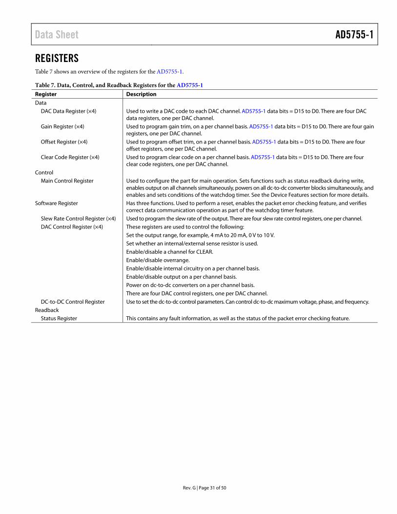
Data Sheet AD5755-1
Rev. G | Page 31 of 50
REGISTERS Table 7 shows an overview of the registers for the AD5755-1.
Table 7. Data, Control, and Readback Registers for the AD5755-1 Register Description Data
DAC Data Register (×4) Used to write a DAC code to each DAC channel. AD5755-1 data bits = D15 to D0. There are four DAC data registers, one per DAC channel.
Gain Register (×4) Used to program gain trim, on a per channel basis. AD5755-1 data bits = D15 to D0. There are four gain registers, one per DAC channel.
Offset Register (×4) Used to program offset trim, on a per channel basis. AD5755-1 data bits = D15 to D0. There are four offset registers, one per DAC channel.
Clear Code Register (×4) Used to program clear code on a per channel basis. AD5755-1 data bits = D15 to D0. There are four clear code registers, one per DAC channel.
Control Main Control Register Used to configure the part for main operation. Sets functions such as status readback during write,
enables output on all channels simultaneously, powers on all dc-to-dc converter blocks simultaneously, and enables and sets conditions of the watchdog timer. See the Device Features section for more details.
Software Register Has three functions. Used to perform a reset, enables the packet error checking feature, and verifies correct data communication operation as part of the watchdog timer feature.
Slew Rate Control Register (×4) Used to program the slew rate of the output. There are four slew rate control registers, one per channel. DAC Control Register (×4) These registers are used to control the following: Set the output range, for example, 4 mA to 20 mA, 0 V to 10 V. Set whether an internal/external sense resistor is used. Enable/disable a channel for CLEAR. Enable/disable overrange. Enable/disable internal circuitry on a per channel basis. Enable/disable output on a per channel basis. Power on dc-to-dc converters on a per channel basis. There are four DAC control registers, one per DAC channel. DC-to-DC Control Register Use to set the dc-to-dc control parameters. Can control dc-to-dc maximum voltage, phase, and frequency.
Readback Status Register This contains any fault information, as well as the status of the packet error checking feature.
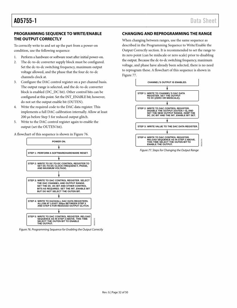
AD5755-1 Data Sheet
Rev. G | Page 32 of 50
PROGRAMMING SEQUENCE TO WRITE/ENABLE THE OUTPUT CORRECTLY To correctly write to and set up the part from a power-on condition, use the following sequence:
1. Perform a hardware or software reset after initial power-on. 2. The dc-to-dc converter supply block must be configured.
Set the dc-to-dc switching frequency, maximum output voltage allowed, and the phase that the four dc-to-dc channels clock at.
3. Configure the DAC control register on a per channel basis. The output range is selected, and the dc-to-dc converter block is enabled (DC_DC bit). Other control bits can be configured at this point. Set the INT_ENABLE bit; however, do not set the output enable bit (OUTEN).
4. Write the required code to the DAC data register. This implements a full DAC calibration internally. Allow at least 200 µs before Step 5 for reduced output glitch.
5. Write to the DAC control register again to enable the output (set the OUTEN bit).
A flowchart of this sequence is shown in Figure 76.
0922
6-07
3
POWER ON.
STEP 1: PERFORM A SOFTWARE/HARDWARE RESET.
STEP 4: WRITE TO EACH/ALL DAC DATA REGISTERS.ALLOW AT LEAST 200µs BETWEEN STEP 3AND STEP 5 FOR REDUCED OUTPUT GLITCH.
STEP 2: WRITE TO DC-TO-DC CONTROL REGISTER TOSET DC-TO-DC CLOCK FREQUENCY, PHASE,AND MAXIMUM VOLTAGE.
STEP 3: WRITE TO DAC CONTROL REGISTER. SELECTTHE DAC CHANNEL AND OUTPUT RANGE.SET THE DC_DC BIT AND OTHER CONTROLBITS AS REQUIRED. SET THE INT_ENABLE BITBUT DO NOT SELECT THE OUTEN BIT.
STEP 5: WRITE TO DAC CONTROL REGISTER. RELOADSEQUENCE AS IN STEP 3 ABOVE. THIS TIMESELECT THE OUTEN BIT TO ENABLETHE OUTPUT.
Figure 76. Programming Sequence for Enabling the Output Correctly
CHANGING AND REPROGRAMMING THE RANGE When changing between ranges, use the same sequence as described in the Programming Sequence to Write/Enable the Output Correctly section. It is recommended to set the range to its zero point (can be midscale or zero scale) prior to disabling the output. Because the dc-to-dc switching frequency, maximum voltage, and phase have already been selected, there is no need to reprogram these. A flowchart of this sequence is shown in Figure 77.
0922
6-07
4
CHANNEL’S OUTPUT IS ENABLED.
STEP 3: WRITE VALUE TO THE DAC DATA REGISTER.
STEP 1: WRITE TO CHANNEL’S DAC DATAREGISTER. SET THE OUTPUTTO 0V (ZERO OR MIDSCALE).
STEP 2: WRITE TO DAC CONTROL REGISTER.DISABLE THE OUTPUT (OUTEN = 0), ANDSET THE NEW OUTPUT RANGE. KEEP THEDC_DC BIT AND THE INT_ENABLE BIT SET.
STEP 4: WRITE TO DAC CONTROL REGISTER.RELOAD SEQUENCE AS IN STEP 2 ABOVE.THIS TIME SELECT THE OUTEN BIT TOENABLE THE OUTPUT.
Figure 77. Steps for Changing the Output Range
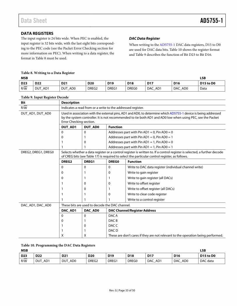
Data Sheet AD5755-1
Rev. G | Page 33 of 50
DATA REGISTERS The input register is 24 bits wide. When PEC is enabled, the input register is 32 bits wide, with the last eight bits correspond-ing to the PEC code (see the Packet Error Checking section for more information on PEC). When writing to a data register, the format in Table 8 must be used.
DAC Data Register
When writing to the AD5755-1 DAC data registers, D15 to D0 are used for DAC data bits. Table 10 shows the register format and Table 9 describes the function of Bit D23 to Bit D16.
Table 8. Writing to a Data Register MSB LSB D23 D22 D21 D20 D19 D18 D17 D16 D15 to D0 R/W DUT_AD1 DUT_AD0 DREG2 DREG1 DREG0 DAC_AD1 DAC_AD0 Data
Table 9. Input Register Decode Bit Description R/W Indicates a read from or a write to the addressed register.
DUT_AD1, DUT_AD0 Used in association with the external pins, AD1 and AD0, to determine which AD5755-1 device is being addressed by the system controller. It is not recommended to tie both AD1 and AD0 low when using PEC, see the Packet Error Checking section.
DUT_AD1 DUT_AD0 Function 0 0 Addresses part with Pin AD1 = 0, Pin AD0 = 0 0 1 Addresses part with Pin AD1 = 0, Pin AD0 = 1 1 0 Addresses part with Pin AD1 = 1, Pin AD0 = 0 1 1 Addresses part with Pin AD1 = 1, Pin AD0 = 1 DREG2, DREG1, DREG0 Selects whether a data register or a control register is written to. If a control register is selected, a further decode
of CREG bits (see Table 17) is required to select the particular control register, as follows.
DREG2 DREG1 DREG0 Function
0 0 0 Write to DAC data register (individual channel write)
0 1 0 Write to gain register
0 1 1 Write to gain register (all DACs)
1 0 0 Write to offset register
1 0 1 Write to offset register (all DACs)
1 1 0 Write to clear code register
1 1 1 Write to a control register
DAC_AD1, DAC_AD0 These bits are used to decode the DAC channel. DAC_AD1 DAC_AD0 DAC Channel/Register Address 0 0 DAC A 0 1 DAC B 1 0 DAC C 1 1 DAC D X X These are don’t cares if they are not relevant to the operation being performed.
Table 10. Programming the DAC Data Registers MSB LSB D23 D22 D21 D20 D19 D18 D17 D16 D15 to D0 R/W DUT_AD1 DUT_AD0 DREG2 DREG1 DREG0 DAC_AD1 DAC_AD0 DAC data
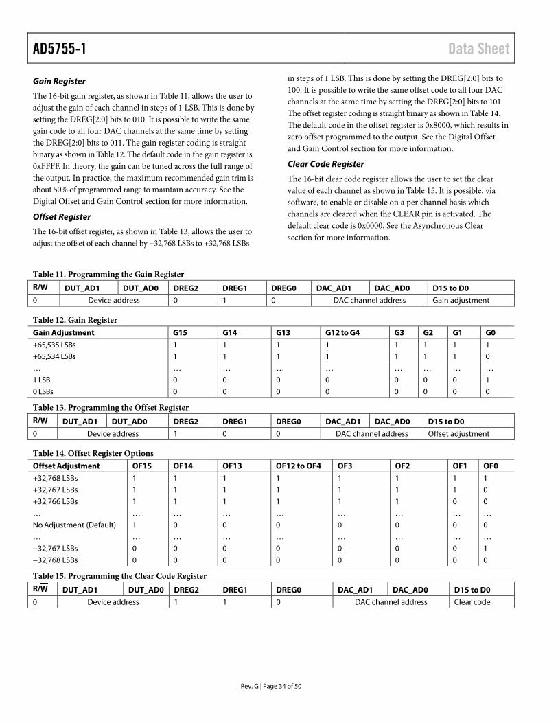
AD5755-1 Data Sheet
Rev. G | Page 34 of 50
Gain Register
The 16-bit gain register, as shown in Table 11, allows the user to adjust the gain of each channel in steps of 1 LSB. This is done by setting the DREG[2:0] bits to 010. It is possible to write the same gain code to all four DAC channels at the same time by setting the DREG[2:0] bits to 011. The gain register coding is straight binary as shown in Table 12. The default code in the gain register is 0xFFFF. In theory, the gain can be tuned across the full range of the output. In practice, the maximum recommended gain trim is about 50% of programmed range to maintain accuracy. See the Digital Offset and Gain Control section for more information.
Offset Register
The 16-bit offset register, as shown in Table 13, allows the user to adjust the offset of each channel by −32,768 LSBs to +32,768 LSBs
in steps of 1 LSB. This is done by setting the DREG[2:0] bits to 100. It is possible to write the same offset code to all four DAC channels at the same time by setting the DREG[2:0] bits to 101. The offset register coding is straight binary as shown in Table 14. The default code in the offset register is 0x8000, which results in zero offset programmed to the output. See the Digital Offset and Gain Control section for more information.
Clear Code Register
The 16-bit clear code register allows the user to set the clear value of each channel as shown in Table 15. It is possible, via software, to enable or disable on a per channel basis which channels are cleared when the CLEAR pin is activated. The default clear code is 0x0000. See the Asynchronous Clear section for more information.
Table 11. Programming the Gain Register R/W DUT_AD1 DUT_AD0 DREG2 DREG1 DREG0 DAC_AD1 DAC_AD0 D15 to D0 0 Device address 0 1 0 DAC channel address Gain adjustment
Table 12. Gain Register Gain Adjustment G15 G14 G13 G12 to G4 G3 G2 G1 G0 +65,535 LSBs 1 1 1 1 1 1 1 1 +65,534 LSBs 1 1 1 1 1 1 1 0 … … … … … … … … … 1 LSB 0 0 0 0 0 0 0 1 0 LSBs 0 0 0 0 0 0 0 0
Table 13. Programming the Offset Register R/W DUT_AD1 DUT_AD0 DREG2 DREG1 DREG0 DAC_AD1 DAC_AD0 D15 to D0 0 Device address 1 0 0 DAC channel address Offset adjustment
Table 14. Offset Register Options Offset Adjustment OF15 OF14 OF13 OF12 to OF4 OF3 OF2 OF1 OF0 +32,768 LSBs 1 1 1 1 1 1 1 1 +32,767 LSBs 1 1 1 1 1 1 1 0 +32,766 LSBs 1 1 1 1 1 1 0 0 … … … … … … … … … No Adjustment (Default) 1 0 0 0 0 0 0 0 … … … … … … … … … −32,767 LSBs 0 0 0 0 0 0 0 1 −32,768 LSBs 0 0 0 0 0 0 0 0
Table 15. Programming the Clear Code Register R/W DUT_AD1 DUT_AD0 DREG2 DREG1 DREG0 DAC_AD1 DAC_AD0 D15 to D0 0 Device address 1 1 0 DAC channel address Clear code
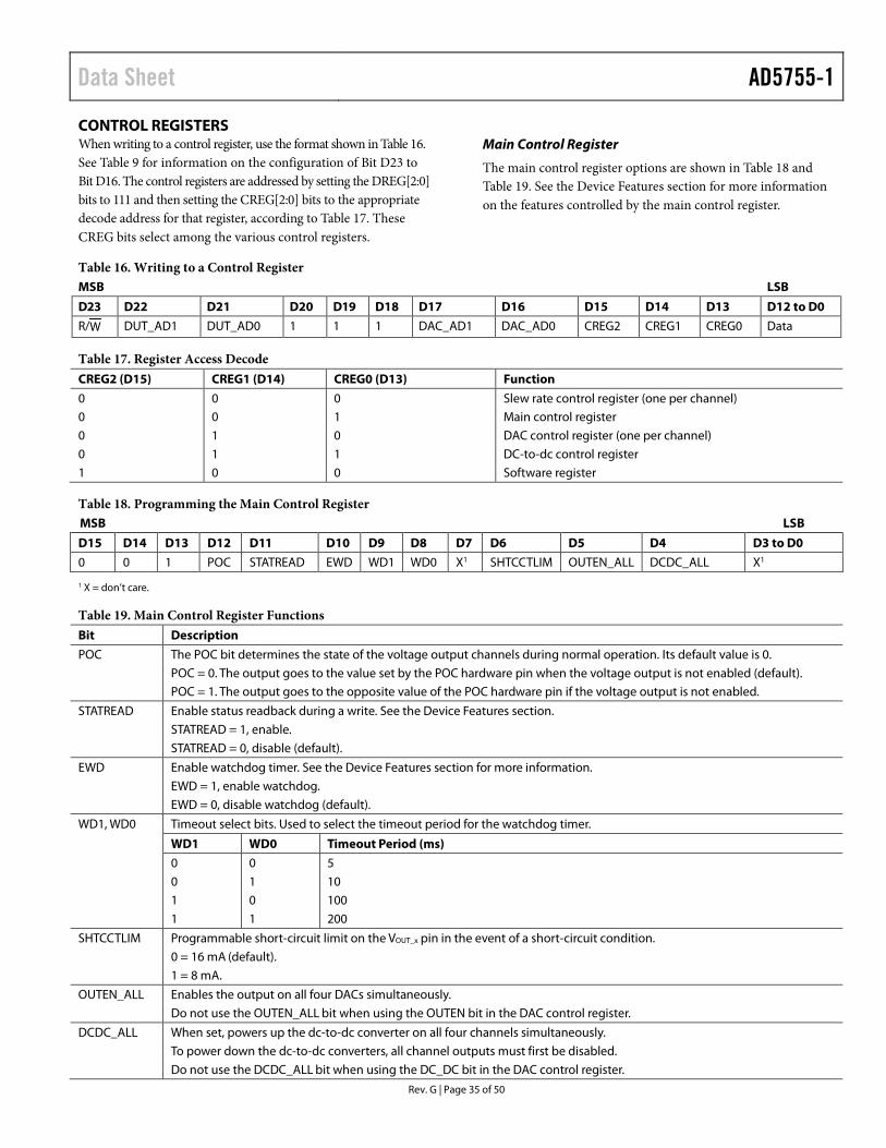
Data Sheet AD5755-1
Rev. G | Page 35 of 50
CONTROL REGISTERS When writing to a control register, use the format shown in Table 16. See Table 9 for information on the configuration of Bit D23 to Bit D16. The control registers are addressed by setting the DREG[2:0] bits to 111 and then setting the CREG[2:0] bits to the appropriate decode address for that register, according to Table 17. These CREG bits select among the various control registers.
Main Control Register
The main control register options are shown in Table 18 and Table 19. See the Device Features section for more information on the features controlled by the main control register.
Table 16. Writing to a Control Register MSB LSB D23 D22 D21 D20 D19 D18 D17 D16 D15 D14 D13 D12 to D0 R/W DUT_AD1 DUT_AD0 1 1 1 DAC_AD1 DAC_AD0 CREG2 CREG1 CREG0 Data
Table 17. Register Access Decode CREG2 (D15) CREG1 (D14) CREG0 (D13) Function 0 0 0 Slew rate control register (one per channel) 0 0 1 Main control register 0 1 0 DAC control register (one per channel) 0 1 1 DC-to-dc control register 1 0 0 Software register
Table 18. Programming the Main Control Register MSB LSB D15 D14 D13 D12 D11 D10 D9 D8 D7 D6 D5 D4 D3 to D0 0 0 1 POC STATREAD EWD WD1 WD0 X1 SHTCCTLIM OUTEN_ALL DCDC_ALL X1
1 X = don’t care.
Table 19. Main Control Register Functions Bit Description POC The POC bit determines the state of the voltage output channels during normal operation. Its default value is 0. POC = 0. The output goes to the value set by the POC hardware pin when the voltage output is not enabled (default). POC = 1. The output goes to the opposite value of the POC hardware pin if the voltage output is not enabled. STATREAD Enable status readback during a write. See the Device Features section. STATREAD = 1, enable. STATREAD = 0, disable (default). EWD Enable watchdog timer. See the Device Features section for more information. EWD = 1, enable watchdog. EWD = 0, disable watchdog (default). WD1, WD0 Timeout select bits. Used to select the timeout period for the watchdog timer. WD1 WD0 Timeout Period (ms) 0 0 5 0 1 10 1 0 100 1 1 200 SHTCCTLIM Programmable short-circuit limit on the VOUT_x pin in the event of a short-circuit condition. 0 = 16 mA (default). 1 = 8 mA. OUTEN_ALL Enables the output on all four DACs simultaneously. Do not use the OUTEN_ALL bit when using the OUTEN bit in the DAC control register. DCDC_ALL When set, powers up the dc-to-dc converter on all four channels simultaneously. To power down the dc-to-dc converters, all channel outputs must first be disabled. Do not use the DCDC_ALL bit when using the DC_DC bit in the DAC control register.

AD5755-1 Data Sheet
Rev. G | Page 36 of 50
DAC Control Register
The DAC control register is used to configure each DAC channel. The DAC control register options are shown in Table 20 and Table 21.
Table 20. Programming DAC Control Register D15 D14 D13 D12 D11 D10 D9 D8 D7 D6 D5 D4 D3 D2 D1 D0 0 1 0 X1 X1 X1 X1 INT_ENABLE CLR_EN OUTEN RSET DC_DC OVRNG R2 R1 R0
1 X = don’t care.
Table 21. DAC Control Register Functions Bit Description INT_ENABLE Powers up the dc-to-dc converter, DAC, and internal amplifiers for the selected channel. Does not enable the output. Can
only be done on a per channel basis. It is recommended to set this bit and allow a >200 µs delay before enabling the output because this results in a reduced output enable glitch. See Figure 31 and Figure 49 for plots of this glitch.
CLR_EN Per channel clear enable bit. Selects if this channel clears when the CLEAR pin is activated. CLR_EN = 1, channel clears when the part is cleared. CLR_EN = 0, channel does not clear when the part is cleared (default). OUTEN Enables/disables the selected output channel. OUTEN = 1, enables the channel. OUTEN = 0, disables the channel (default). RSET Selects an internal or external current sense resistor for the selected DAC channel. RSET = 0, selects the external resistor (default). RSET = 1, selects the internal resistor. DC_DC Powers the dc-to-dc converter on the selected channel. DC_DC = 1, power up the dc-to-dc converter. DC_DC = 0, power down the dc-to-dc converter (default). This allows per channel dc-to-dc converter power-up/power-down. To power down the dc-to-dc converter, the OUTEN and
INT_ENABLE bits must also be set to 0. All dc-to-dc converters can also be powered up simultaneously using the DCDC_ALL bit in the main control register. OVRNG Enables 20% overrange on voltage output channel only. No current output overrange available. OVRNG = 1, enabled. OVRNG = 0, disabled (default). R2, R1, R0 Selects the output range to be enabled. R2 R1 R0 Output Range Selected 0 0 0 0 V to 5 V voltage range (default). 0 0 1 0 V to 10 V voltage range. 0 1 0 ±5 V voltage range. 0 1 1 ±10 V voltage range. 1 0 0 4 mA to 20 mA current range. 1 0 1 0 mA to 20 mA current range. 1 1 0 0 mA to 24 mA current range.

Data Sheet AD5755-1
Rev. G | Page 37 of 50
Software Register
The software register has three functions. It allows the user to perform a software reset to the device and enable the packet error checking feature (see the Packet Error Checking section) It is also used as part of the watchdog feature when it is enabled. This feature is useful to ensure that communication is not lost between the MCU and the AD5755-1 and that the datapath lines are working properly (that is, SDIN, SCLK, and SYNC).
When the watchdog feature is enabled, the user must write 0x195 to the software register within the timeout period. If this command is not received within the timeout period, the ALERT pin signals a fault condition. This is only required when the watchdog timer function is enabled.
DC-to-DC Control Register
The dc-to-dc control register allows the user control over the dc-to-dc switching frequency and phase, as well as the maximum allowable dc-to-dc output voltage. The dc-to-dc control register options are shown in Table 24 and Table 25.
Table 22. Programming the Software Register MSB LSB D15 D14 D13 D12 D11 to D0 1 0 0 PEC enable Reset code/SPI code
Table 23. Software Register Functions Bit Description PEC Enable This bit selects if the packet error checking feature is enabled (see the Packet Error Checking section). 0 = PEC disabled. 1 = PEC enabled. Reset Code/SPI Code Option Description Reset code Writing 0x555 to D[11:0] performs a reset of the AD5755-1. SPI code If the watchdog timer feature is enabled, 0x195 must be written to the software register
(D11 to D0) within the programmed timeout period.
Table 24. Programming the DC-to-DC Control Register MSB LSB D15 D14 D13 D12 to D7 D6 D5 to D4 D3 to D2 D1 to D0 0 1 1 X1 DC-DC Comp DC-DC phase DC-DC Freq DC-DC MaxV
1 X = don’t care.
Table 25. DC-to-DC Control Register Options Bit Description DC-DC Comp Selects between an internal and external compensation resistor for the dc-to-dc converter. See the DC-to-DC Converter
Compensation Capacitors and AICC Supply Requirements—Slewing sections in the Device Features section for more information.
0 = selects the internal 150 kΩ compensation resistor (default). 1 = bypasses the internal compensation resistor for the dc-to-dc converter. In this mode, an external dc-to-dc compensation
resistor must be used; this is placed at the COMPDCDC_x pin in series with the 10 nF dc-to-dc compensation capacitor to ground. Typically, a ~50 kΩ resistor is recommended.
DC-DC Phase User programmable dc-to-dc converter phase (between channels). 00 = all dc-to-dc converters clock on the same edge (default). 01 = Channel A and Channel B clock on the same edge, Channel C and Channel D clock on opposite edges. 10 = Channel A and Channel C clock on the same edge, Channel B and Channel D clock on opposite edges. 11 = Channel A, Channel B, Channel C, and Channel D clock 90° out of phase from each other. DC-DC Freq DC-to-dc switching frequency; these are divided down from the internal 13 MHz oscillator (see Figure 70 and Figure 71). 00 = 250 ± 10% kHz. 01 = 410 ± 10% kHz (default). 10 = 650 ± 10% kHz. DC-DC MaxV Maximum allowed VBOOST_x voltage supplied by the dc-to-dc converter. 00 = 23 V + 1 V/−1.5 V (default). 01 = 24.5 V ± 1 V. 10 = 27 V ± 1 V. 11 = 29.5 V ± 1 V.
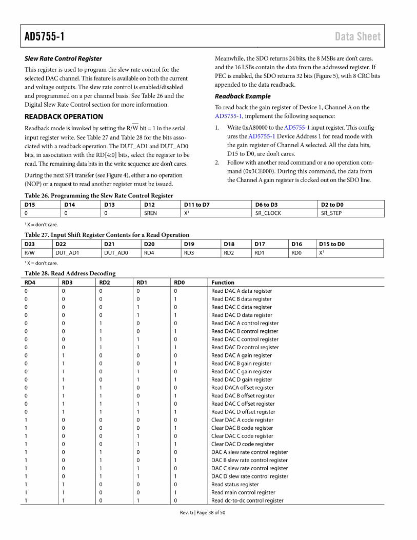
AD5755-1 Data Sheet
Rev. G | Page 38 of 50
Slew Rate Control Register
This register is used to program the slew rate control for the selected DAC channel. This feature is available on both the current and voltage outputs. The slew rate control is enabled/disabled and programmed on a per channel basis. See Table 26 and the Digital Slew Rate Control section for more information.
READBACK OPERATION Readback mode is invoked by setting the R/W bit = 1 in the serial input register write. See Table 27 and Table 28 for the bits asso-ciated with a readback operation. The DUT_AD1 and DUT_AD0 bits, in association with the RD[4:0] bits, select the register to be read. The remaining data bits in the write sequence are don’t cares.
During the next SPI transfer (see Figure 4), either a no operation (NOP) or a request to read another register must be issued.
Meanwhile, the SDO returns 24 bits, the 8 MSBs are don’t cares, and the 16 LSBs contain the data from the addressed register. If PEC is enabled, the SDO returns 32 bits (Figure 5), with 8 CRC bits appended to the data readback.
Readback Example
To read back the gain register of Device 1, Channel A on the AD5755-1, implement the following sequence:
1. Write 0xA80000 to the AD5755-1 input register. This config-ures the AD5755-1 Device Address 1 for read mode with the gain register of Channel A selected. All the data bits, D15 to D0, are don’t cares.
2. Follow with another read command or a no operation com-mand (0x3CE000). During this command, the data from the Channel A gain register is clocked out on the SDO line.
Table 26. Programming the Slew Rate Control Register D15 D14 D13 D12 D11 to D7 D6 to D3 D2 to D0 0 0 0 SREN X1 SR_CLOCK SR_STEP
1 X = don’t care.
Table 27. Input Shift Register Contents for a Read Operation D23 D22 D21 D20 D19 D18 D17 D16 D15 to D0 R/W DUT_AD1 DUT_AD0 RD4 RD3 RD2 RD1 RD0 X1 1 X = don’t care.
Table 28. Read Address Decoding RD4 RD3 RD2 RD1 RD0 Function 0 0 0 0 0 Read DAC A data register 0 0 0 0 1 Read DAC B data register 0 0 0 1 0 Read DAC C data register 0 0 0 1 1 Read DAC D data register 0 0 1 0 0 Read DAC A control register 0 0 1 0 1 Read DAC B control register 0 0 1 1 0 Read DAC C control register 0 0 1 1 1 Read DAC D control register 0 1 0 0 0 Read DAC A gain register 0 1 0 0 1 Read DAC B gain register 0 1 0 1 0 Read DAC C gain register 0 1 0 1 1 Read DAC D gain register 0 1 1 0 0 Read DACA offset register 0 1 1 0 1 Read DAC B offset register 0 1 1 1 0 Read DAC C offset register 0 1 1 1 1 Read DAC D offset register 1 0 0 0 0 Clear DAC A code register 1 0 0 0 1 Clear DAC B code register 1 0 0 1 0 Clear DAC C code register 1 0 0 1 1 Clear DAC D code register 1 0 1 0 0 DAC A slew rate control register 1 0 1 0 1 DAC B slew rate control register 1 0 1 1 0 DAC C slew rate control register 1 0 1 1 1 DAC D slew rate control register 1 1 0 0 0 Read status register 1 1 0 0 1 Read main control register 1 1 0 1 0 Read dc-to-dc control register
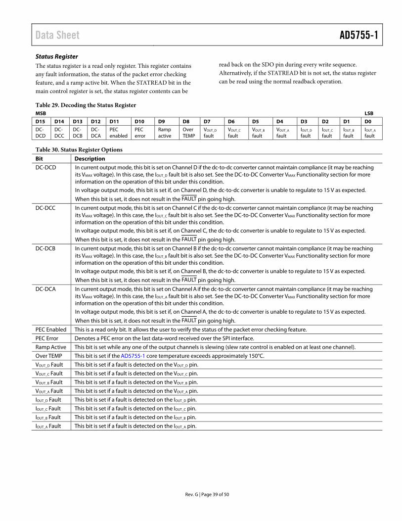
Data Sheet AD5755-1
Rev. G | Page 39 of 50
Status Register The status register is a read only register. This register contains any fault information, the status of the packet error checking feature, and a ramp active bit. When the STATREAD bit in the main control register is set, the status register contents can be
read back on the SDO pin during every write sequence. Alternatively, if the STATREAD bit is not set, the status register can be read using the normal readback operation.
Table 29. Decoding the Status Register MSB LSB D15 D14 D13 D12 D11 D10 D9 D8 D7 D6 D5 D4 D3 D2 D1 D0 DC-DCD
DC-DCC
DC-DCB
DC-DCA
PEC enabled
PEC error
Ramp active
Over TEMP
VOUT_D fault
VOUT_C fault
VOUT_B fault
VOUT_A fault
IOUT_D fault
IOUT_C fault
IOUT_B fault
IOUT_A fault
Table 30. Status Register Options Bit Description DC-DCD In current output mode, this bit is set on Channel D if the dc-to-dc converter cannot maintain compliance (it may be reaching
its VMAX voltage). In this case, the IOUT_D fault bit is also set. See the DC-to-DC Converter VMAX Functionality section for more information on the operation of this bit under this condition.
In voltage output mode, this bit is set if, on Channel D, the dc-to-dc converter is unable to regulate to 15 V as expected. When this bit is set, it does not result in the FAULT pin going high. DC-DCC In current output mode, this bit is set on Channel C if the dc-to-dc converter cannot maintain compliance (it may be reaching
its VMAX voltage). In this case, the IOUT_C fault bit is also set. See the DC-to-DC Converter VMAX Functionality section for more information on the operation of this bit under this condition.
In voltage output mode, this bit is set if, on Channel C, the dc-to-dc converter is unable to regulate to 15 V as expected. When this bit is set, it does not result in the FAULT pin going high. DC-DCB In current output mode, this bit is set on Channel B if the dc-to-dc converter cannot maintain compliance (it may be reaching
its VMAX voltage). In this case, the IOUT_B fault bit is also set. See the DC-to-DC Converter VMAX Functionality section for more information on the operation of this bit under this condition.
In voltage output mode, this bit is set if, on Channel B, the dc-to-dc converter is unable to regulate to 15 V as expected. When this bit is set, it does not result in the FAULT pin going high.
DC-DCA In current output mode, this bit is set on Channel A if the dc-to-dc converter cannot maintain compliance (it may be reaching its VMAX voltage). In this case, the IOUT_A fault bit is also set. See the DC-to-DC Converter VMAX Functionality section for more information on the operation of this bit under this condition.
In voltage output mode, this bit is set if, on Channel A, the dc-to-dc converter is unable to regulate to 15 V as expected. When this bit is set, it does not result in the FAULT pin going high. PEC Enabled This is a read only bit. It allows the user to verify the status of the packet error checking feature. PEC Error Denotes a PEC error on the last data-word received over the SPI interface. Ramp Active This bit is set while any one of the output channels is slewing (slew rate control is enabled on at least one channel). Over TEMP This bit is set if the AD5755-1 core temperature exceeds approximately 150°C. VOUT_D Fault This bit is set if a fault is detected on the VOUT_D pin. VOUT_C Fault This bit is set if a fault is detected on the VOUT_C pin. VOUT_B Fault This bit is set if a fault is detected on the VOUT_B pin. VOUT_A Fault This bit is set if a fault is detected on the VOUT_A pin. IOUT_D Fault This bit is set if a fault is detected on the IOUT_D pin. IOUT_C Fault This bit is set if a fault is detected on the IOUT_C pin. IOUT_B Fault This bit is set if a fault is detected on the IOUT_B pin. IOUT_A Fault This bit is set if a fault is detected on the IOUT_A pin.
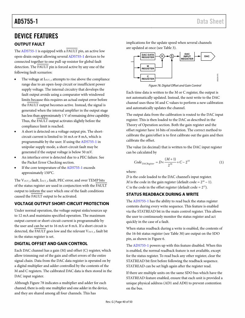
AD5755-1 Data Sheet
Rev. G | Page 40 of 50
DEVICE FEATURES OUTPUT FAULT The AD5755-1 is equipped with a FAULT pin, an active low open-drain output allowing several AD5755-1 devices to be connected together to one pull-up resistor for global fault detection. The FAULT pin is forced active by any one of the following fault scenarios:
• The voltage at IOUT_x attempts to rise above the compliance range due to an open-loop circuit or insufficient power supply voltage. The internal circuitry that develops the fault output avoids using a comparator with windowed limits because this requires an actual output error before the FAULT output becomes active. Instead, the signal is generated when the internal amplifier in the output stage has less than approximately 1 V of remaining drive capability. Thus, the FAULT output activates slightly before the compliance limit is reached.
• A short is detected on a voltage output pin. The short-circuit current is limited to 16 mA or 8 mA, which is programmable by the user. If using the AD5755-1 in unipolar supply mode, a short-circuit fault may be generated if the output voltage is below 50 mV.
• An interface error is detected due to a PEC failure. See the Packet Error Checking section.
• If the core temperature of the AD5755-1 exceeds approximately 150°C.
The VOUT_x fault, IOUT_x fault, PEC error, and over TEMP bits of the status register are used in conjunction with the FAULT output to inform the user which one of the fault conditions caused the FAULT output to be activated.
VOLTAGE OUTPUT SHORT-CIRCUIT PROTECTION Under normal operation, the voltage output sinks/sources up to 12 mA and maintains specified operation. The maximum output current or short-circuit current is programmable by the user and can be set to 16 mA or 8 mA. If a short circuit is detected, the FAULT goes low and the relevant VOUT_x fault bit in the status register is set.
DIGITAL OFFSET AND GAIN CONTROL Each DAC channel has a gain (M) and offset (C) register, which allow trimming out of the gain and offset errors of the entire signal chain. Data from the DAC data register is operated on by a digital multiplier and adder controlled by the contents of the M and C registers. The calibrated DAC data is then stored in the DAC input register.
Although Figure 78 indicates a multiplier and adder for each channel, there is only one multiplier and one adder in the device, and they are shared among all four channels. This has
implications for the update speed when several channels are updated at once (see Table 3).
0922
6-07
5
DACINPUT
REGISTERDACDAC DATA
REGISTER
MREGISTER
CREGISTER
Figure 78. Digital Offset and Gain Control
Each time data is written to the M or C register, the output is not automatically updated. Instead, the next write to the DAC channel uses these M and C values to perform a new calibration and automatically updates the channel.
The output data from the calibration is routed to the DAC input register. This is then loaded to the DAC as described in the Theory of Operation section. Both the gain register and the offset register have 16 bits of resolution. The correct method to calibrate the gain/offset is to first calibrate out the gain and then calibrate the offset.
The value (in decimal) that is written to the DAC input register can be calculated by
1516 2
2)1(
−++
×= CM
DCode rDACRegiste (1)
where: D is the code loaded to the DAC channel’s input register. M is the code in the gain register (default code = 216 – 1). C is the code in the offset register (default code = 215).
STATUS READBACK DURING A WRITE The AD5755-1 has the ability to read back the status register contents during every write sequence. This feature is enabled via the STATREAD bit in the main control register. This allows the user to continuously monitor the status register and act quickly in the case of a fault.
When status readback during a write is enabled, the contents of the 16-bit status register (see Table 30) are output on the SDO pin, as shown in Figure 6.
The AD5755-1 powers up with this feature disabled. When this is enabled, the normal readback feature is not available, except for the status register. To read back any other register, clear the STATREAD bit first before following the readback sequence. STATREAD can be set high again after the register read.
If there are multiple units on the same SDO bus which have the STATREAD feature enabled, ensure that each unit is provided a unique physical address (AD1 and AD0) to prevent contention on the bus.
Data Sheet AD5755-1
Rev. G | Page 41 of 50
ASYNCHRONOUS CLEAR CLEAR is an active high, edge-sensitive input that allows the output to be cleared to a preprogrammed 16-bit code. This code is user programmable via a per channel 16-bit clear code register.
For a channel to clear, that channel must be enabled to be cleared via the CLR_EN bit in the channel’s DAC control register. If the channel is not enabled to be cleared, then the output remains in its current state independent of the CLEAR pin level. When the CLEAR signal is returned low, the relevant outputs remain cleared until a new value is programmed.
PACKET ERROR CHECKING To verify that data has been received correctly in noisy environ-ments, the AD5755-1 offers the option of packet error checking based on an 8-bit cyclic redundancy check (CRC-8). The device controlling the AD5755-1 generates an 8-bit frame check sequence using the polynomial
C(x) = x8 + x2 + x1 + 1
This is added to the end of the data-word, and 32 bits are sent to the AD5755-1 before taking SYNC high. If the packet error checking enable bit is set high (Bit 12 in the software register), the user must supply a 32-bit frame that contains the 24 data bits and 8-bit CRC. If the check is valid, the data is written to the selected register. If the error check fails, the FAULT pin goes low and the PEC error bit in the status register is set. After reading the status register, FAULT returns high (assuming there are no other faults), and the PEC error bit is cleared automati-cally. It is not recommended to tie both AD1 and AD0 low because a short low on SDIN, that is, a command of 16 zeroes, may possibly lead to a zero-scale update for DAC A. The PEC can be used for both transmit and receive of data packets.
SDIN
SYNC
SCLK
UPDATE ON SYNC HIGH
MSBD23
LSBD0
24-BIT DATA
24-BIT DATA TRANSFER—NO ERROR CHECKING
SDIN
FAULT
SYNC
SCLK
UPDATE ON SYNC HIGHONLY IF ERROR CHECK PASSED
FAULT PIN GOES LOWIF ERROR CHECK FAILS
MSBD31
LSBD8 D7 D0
24-BIT DATA 8-BIT CRC
32-BIT DATA TRANSFER WITH ERROR CHECKING 0922
6-18
0
Figure 79. PEC Timing
WATCHDOG TIMER When enabled, an on-chip watchdog timer generates an alert signal if 0x195 has not been written to the software register within the programmed timeout period. This feature is useful to ensure that communication is not lost between the MCU and the AD5755-1 and that these datapath lines are working properly (that is, SDIN, SCLK, and SYNC). If 0x195 is not received by the software register within the timeout period, the ALERT pin signals a fault condition. The ALERT signal is active high and can be connected directly to the CLEAR pin to enable a clear in the event that communication from the MCU is lost.
The watchdog timer is enabled, and the timeout period (5 ms, 10 ms, 100 ms, or 200 ms) is set in the main control register (see Table 18 and Table 19).
OUTPUT ALERT The AD5755-1 is equipped with an ALERT pin. This is an active high CMOS output. The AD5755-1 also has an internal watchdog timer. When enabled, it monitors SPI communications. If 0x195 is not received by the software register within the timeout period, the ALERT pin goes active.
INTERNAL REFERENCE The AD5755-1 contains an integrated +5 V voltage reference with initial accuracy of ±5 mV maximum and a temperature drift coefficient of ±10 ppm maximum. The reference voltage is buffered and externally available for use elsewhere within the system. REFOUT must be connected to REFIN to use the internal reference.
EXTERNAL CURRENT SETTING RESISTOR Referring to Figure 74, RSET is an internal sense resistor as part of the voltage-to-current conversion circuitry. The stability of the output current value over temperature is dependent on the stability of the value of RSET. As a method of improving the stability of the output current over temperature, an external 15 kΩ low drift resistor can be connected to the RSET_x pin of the AD5755-1 to be used instead of the internal resistor, R1. The external resistor is selected via the DAC control register (see Table 20).
Table 1 outlines the performance specifications of the AD5755-1 with both the internal RSET resistor and an external, 15 kΩ RSET resistor. Using an external RSET resistor allows for improved performance over the internal RSET resistor option. The external RSET resistor specification assumes an ideal resistor; the actual performance depends on the absolute value and temperature coefficient of the resistor used. This directly affects the gain error of the output, and thus the total unadjusted error. To arrive at the gain/TUE error of the output with a particular external RSET resistor, add the percentage absolute error of the RSET resistor directly to the gain/TUE error of the AD5755-1 with the exter-nal RSET resistor, shown in Table 1 (expressed in % FSR).
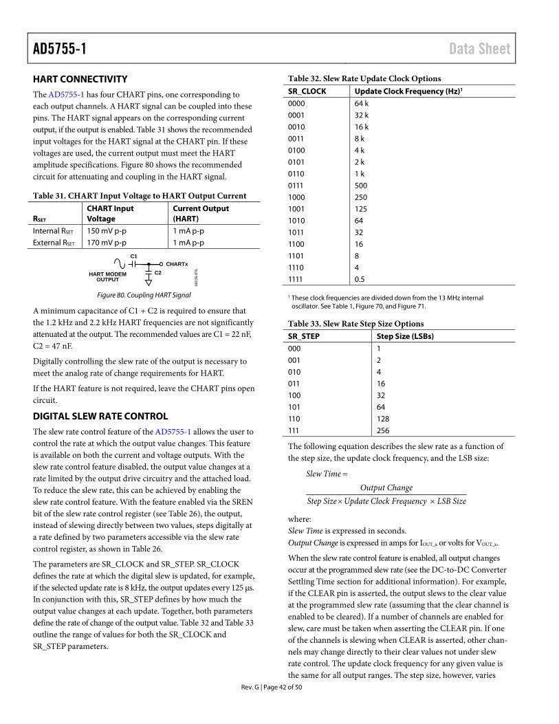
AD5755-1 Data Sheet
Rev. G | Page 42 of 50
HART CONNECTIVITY The AD5755-1 has four CHART pins, one corresponding to each output channels. A HART signal can be coupled into these pins. The HART signal appears on the corresponding current output, if the output is enabled. Table 31 shows the recommended input voltages for the HART signal at the CHART pin. If these voltages are used, the current output must meet the HART amplitude specifications. Figure 80 shows the recommended circuit for attenuating and coupling in the HART signal.
Table 31. CHART Input Voltage to HART Output Current
RSET CHART Input Voltage
Current Output (HART)
Internal RSET 150 mV p-p 1 mA p-p External RSET 170 mV p-p 1 mA p-p
0922
6-07
6
HART MODEMOUTPUT
C1
C2CHARTx
Figure 80. Coupling HART Signal
A minimum capacitance of C1 + C2 is required to ensure that the 1.2 kHz and 2.2 kHz HART frequencies are not significantly attenuated at the output. The recommended values are C1 = 22 nF, C2 = 47 nF.
Digitally controlling the slew rate of the output is necessary to meet the analog rate of change requirements for HART.
If the HART feature is not required, leave the CHART pins open circuit.
DIGITAL SLEW RATE CONTROL The slew rate control feature of the AD5755-1 allows the user to control the rate at which the output value changes. This feature is available on both the current and voltage outputs. With the slew rate control feature disabled, the output value changes at a rate limited by the output drive circuitry and the attached load. To reduce the slew rate, this can be achieved by enabling the slew rate control feature. With the feature enabled via the SREN bit of the slew rate control register (see Table 26), the output, instead of slewing directly between two values, steps digitally at a rate defined by two parameters accessible via the slew rate control register, as shown in Table 26.
The parameters are SR_CLOCK and SR_STEP. SR_CLOCK defines the rate at which the digital slew is updated, for example, if the selected update rate is 8 kHz, the output updates every 125 µs. In conjunction with this, SR_STEP defines by how much the output value changes at each update. Together, both parameters define the rate of change of the output value. Table 32 and Table 33 outline the range of values for both the SR_CLOCK and SR_STEP parameters.
Table 32. Slew Rate Update Clock Options SR_CLOCK Update Clock Frequency (Hz)1 0000 64 k 0001 32 k 0010 16 k 0011 8 k 0100 4 k 0101 2 k 0110 1 k 0111 500 1000 250 1001 125 1010 64 1011 32 1100 16 1101 8 1110 4 1111 0.5 1 These clock frequencies are divided down from the 13 MHz internal
oscillator. See Table 1, Figure 70, and Figure 71.
Table 33. Slew Rate Step Size Options SR_STEP Step Size (LSBs) 000 1 001 2 010 4 011 16 100 32 101 64 110 128 111 256
The following equation describes the slew rate as a function of the step size, the update clock frequency, and the LSB size:
SizeLSBFrequencyClockUpdateSizeStepChangeOutput
TimeSlew
××
=
where: Slew Time is expressed in seconds. Output Change is expressed in amps for IOUT_x or volts for VOUT_x.
When the slew rate control feature is enabled, all output changes occur at the programmed slew rate (see the DC-to-DC Converter Settling Time section for additional information). For example, if the CLEAR pin is asserted, the output slews to the clear value at the programmed slew rate (assuming that the clear channel is enabled to be cleared). If a number of channels are enabled for slew, care must be taken when asserting the CLEAR pin. If one of the channels is slewing when CLEAR is asserted, other chan-nels may change directly to their clear values not under slew rate control. The update clock frequency for any given value is the same for all output ranges. The step size, however, varies

Data Sheet AD5755-1
Rev. G | Page 43 of 50
across output ranges for a given value of step size because the LSB size is different for each output range.
POWER DISSIPATION CONTROL The AD5755-1 contains integrated dynamic power control using a dc-to-dc boost converter circuit, allowing reductions in power consumption from standard designs when using the part in current output mode.
In standard current input module designs, the load resistor values can range from typically 50 Ω to 750 Ω. Output module systems must source enough voltage to meet the compliance voltage requirement across the full range of load resistor values. For example, in a 4 mA to 20 mA loop when driving 20 mA, a compliance voltage of >15 V is required. When driving 20 mA into a 50 Ω load, only 1 V compliance is required.
The AD5755-1 circuitry senses the output voltage and regulates this voltage to meet compliance requirements plus a small headroom voltage. The AD5755-1 is capable of driving up to 24 mA through a 1 kΩ load.
DC-TO-DC CONVERTERS The AD5755-1 contains four independent dc-to-dc converters. These are used to provide dynamic control of the VBOOST supply voltage for each channel (see Figure 74). Figure 81 shows the discrete components needed for the dc-to-dc circuitry, and the following sections describe component selection and operation of this circuitry.
AVCCLDCDC DDCDC
CDCDC4.7µF
CFILTER0.1µF
RFILTER
CIN
SWx
VBOOST_X
≥10µF10Ω10µH
0922
6-07
7
Figure 81. DC-to-DC Circuit
Table 34. Recommended DC-to-DC Components Symbol Component Value Manufacturer LDCDC XAL4040-103 10 µH Coilcraft® CDCDC GRM32ER71H475KA88L 4.7 µF Murata DDCDC PD3S160-7 0.55 VF Diodes, Inc.
It is recommended to place a 10 Ω, 100 nF low-pass RC filter after CDCDC. This consumes a small amount of power but reduces the amount of ripple on the VBOOST_x supply.
DC-to-DC Converter Operation
The on-board dc-to-dc converters use a constant frequency, peak current mode control scheme to step up an AVCC input of 4.5 V to 5.5 V to drive the AD5755-1 output channel. These are designed to operate in discontinuous conduction mode (DCM) with a duty cycle of <90% typical. Discontinuous conduction mode refers to a mode of operation where the inductor current goes to zero for an appreciable percentage of the switching cycle. The dc-to-dc converters are nonsynchronous; that is, they require an external Schottky diode.
DC-to-DC Converter Output Voltage
When a channel current output is enabled, the converter regulates the VBOOST_x supply to 7.4 V (±5%) or (IOUT × RLOAD + Headroom), whichever is greater (see Figure 54 for a plot of headroom supplied vs. output current). In voltage output mode with the output disabled, the converter regulates the VBOOST_x supply to +15 V (±5%). In current output mode with the output disabled, the converter regulates the VBOOST_x supply to 7.4 V (±5%).
Within a channel, the VOUT_x and IOUT_x stages share a common VBOOST_x supply so that the outputs of the IOUT_x and VOUT_x stages can be tied together.
DC-to-DC Converter Settling Time
When in current output mode, the settling time for a step greater than ~1 V (IOUT × RLOAD) is dominated by the settling time of the dc-to-dc converter. The exception to this is when the required voltage at the IOUT_x pin plus the compliance voltage is below 7.4 V (±5%). A typical plot of the output settling time can be found in Figure 50. This plot is for a 1 kΩ load. The settling time for smaller loads is faster. The settling time for current steps less than 24 mA is also faster.
DC-to-DC Converter VMAX Functionality
The maximum VBOOST_x voltage is set in the dc-to-dc control register (23 V, 24.5 V, 27 V, or 29.5 V; see Table 25). On reaching this maximum voltage, the dc-to-dc converter is disabled, and the VBOOST_x voltage is allowed to decay by ~0.4 V. After the VBOOST_x voltage has decayed by ~0.4 V, the dc-to-dc converter is reenabled, and the voltage ramps up again to VMAX, if still required. This operation is shown in Figure 82.
28.6
28.7
28.8
28.9
29.0
29.1
29.2
29.3
29.4
29.5
29.6
0 0.5 1.0 1.5 2.0 2.5 3.0 3.5 4.0
V BO
OST
VO
LTA
GE
(V)
TIME (ms)
VMAX 0mA TO 24mA RANGE, 24mA OUTPUTOUTPUT UNLOADED
DC-DCMaxV = 11 (29.5V)
DC_DC BIT
0922
6-18
3
DCDCx BIT = 0
DCDCx BIT = 1
fSW = 410kHzTA = 25°C
Figure 82. Operation on Reaching VMAX
As can be seen in Figure 82, the DC-DCx bit in the status register asserts when the AD5755-1 is ramping to the VMAX value but deasserts when the voltage is decaying to VMAX − ~0.4 V.
AD5755-1 Data Sheet
Rev. G | Page 44 of 50
DC-to-DC Converter On-Board Switch
The AD5755-1 contains a 0.425 Ω internal switch. The switch current is monitored on a pulse by pulse basis and is limited to 0.8 A peak current.
DC-to-DC Converter Switching Frequency and Phase
The AD5755-1 dc-to-dc converter switching frequency can be selected from the dc-to-dc control register. The phasing of the channels can also be adjusted so that the dc-to-dc converter can clock on different edges (see Table 25). For typical applications, a 410 kHz frequency is recommended. At light loads (low output current and small load resistor), the dc-to-dc converter enters a pulse-skipping mode to minimize switching power dissipation.
DC-to-DC Converter Inductor Selection
For typical 4 mA to 20 mA applications, a 10 µH inductor (such as the XAL4040-103 from Coilcraft), combined with a switching frequency of 410 kHz, allows up to 24 mA to be driven into a load resistance of up to 1 kΩ with an AVCC supply of 4.5 V to 5.5 V. It is important to ensure that the inductor is able to handle the peak current without saturating, especially at the maximum ambient temperature. If the inductor enters into saturation mode, it results in a decrease in efficiency. The inductance value also drops during saturation and may result in the dc-to-dc converter circuit not being able to supply the required output power.
DC-to-DC Converter External Schottky Selection
The AD5755-1 requires an external Schottky for correct operation. Ensure that the Schottky is rated to handle the maximum reverse breakdown expected in operation and that the rectifier maximum junction temperature is not exceeded. The diode average current is approximately equal to the ILOAD current. Diodes with larger forward voltage drops result in a decrease in efficiency.
DC-to-DC Converter Compensation Capacitors
As the dc-to-dc converter operates in DCM, the uncompensated transfer function is essentially a single-pole transfer function. The pole frequency of the transfer function is determined by the output capacitance of the dc-to-dc converter, input and output voltage, and output load. The AD5755-1 uses an external capacitor in conjunction with an internal 150 kΩ resistor to compensate the regulator loop. Alternatively, an external compensation resistor can be used in series with the compensation capacitor, by setting the DC-DC Comp bit in the dc-to-dc control register. In this case, a ~50 kΩ resistor is recommended. A description of the advantages of this can be found in the AICC Supply Requirements—Slewing section. For typical applications, a 10 nF dc-to-dc compensation capacitor is recommended.
DC-to-DC Converter Input and Output Capacitor Selection
The output capacitor affects ripple voltage of the dc-to-dc converter and indirectly limits the maximum slew rate at which
the channel output current can rise. The ripple voltage is caused by a combination of the capacitance and equivalent series resistance (ESR) of the capacitor. For the AD5755-1, a ceramic capacitor of 4.7 µF is recommended for typical applications.
Larger capacitors or paralleled capacitors improve the ripple at the expense of reduced slew rate. Larger capacitors also impact the AVCC supplies current requirements while slewing (see the AICC Supply Requirements—Slewing section). This capacitance at the output of the dc-to-dc converter must be >3 µF under all operating conditions.
The input capacitor provides much of the dynamic current required for the dc-to-dc converter and must be a low ESR component. For the AD5755-1, a low ESR tantalum or ceramic capacitor of 10 µF is recommended for typical applications. Ceramic capacitors must be chosen carefully because they can exhibit a large sensitivity to dc bias voltages and temperature. X5R or X7R dielectrics are preferred because these capacitors remain stable over wider operating voltage and temperature ranges. Care must be taken if selecting a tantalum capacitor to ensure a low ESR value.
AICC SUPPLY REQUIREMENTS—STATIC The dc-to-dc converter is designed to supply a VBOOST_x voltage of
VBOOST = IOUT × RLOAD + Headroom (2)
See Figure 54 for a plot of headroom supplied vs. output voltage. This means that, for a fixed load and output voltage, the dc-to-dc converter output current can be calculated by the following formula:
CCV
BOOSTOUT
CCCC AV
VIAVEfficiency
OutPowerAI
BOOST×
×=
×=
η (3)
where: IOUT is the output current from IOUT_x in amps. ηVBOOST is the efficiency at VBOOST_x as a fraction (see Figure 56
and Figure 57).
AICC SUPPLY REQUIREMENTS—SLEWING The AICC current requirement while slewing is greater than in static operation because the output power increases to charge the output capacitance of the dc-to-dc converter. This transient current can be quite large (see Figure 83), although the methods described in the Reducing AICC Current Requirements section can reduce the requirements on the AVCC supply. If not enough AICC current can be provided, the AVCC voltage drops. Due to this AVCC drop, the AICC current required to slew increases further. This means that the voltage at AVCC drops further (see Equation 3) and the VBOOST_x voltage, and thus the output voltage, may never reach its intended value. Because this AVCC voltage is common to all channels, this may also affect other channels.
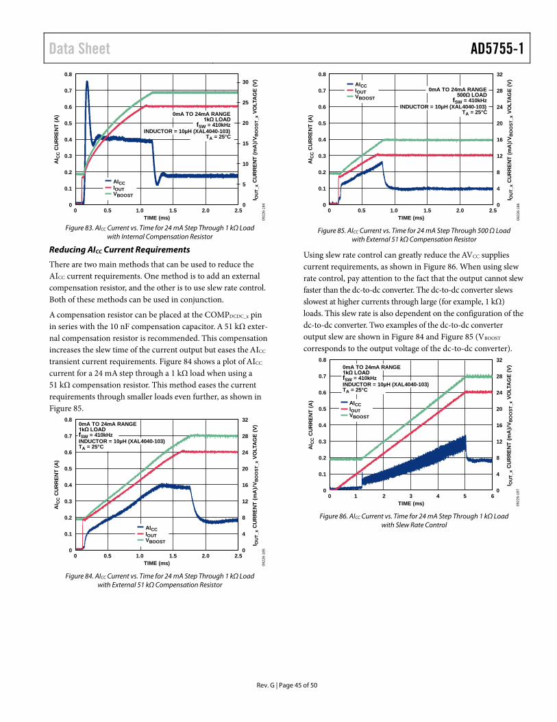
Data Sheet AD5755-1
Rev. G | Page 45 of 50
0
5
10
15
20
25
30
0
0.1
0.2
0.3
0.4
0.5
0.6
0.7
0.8
0 0.5 1.0 1.5 2.0 2.5
I OU
T_x
CU
RR
ENT
(mA
)/V B
OO
ST_x
VO
LTA
GE
(V)
AI C
C C
UR
REN
T (A
)
TIME (ms)
AICCIOUTVBOOST
0mA TO 24mA RANGE1kΩ LOAD
fSW = 410kHzINDUCTOR = 10µH (XAL4040-103)
TA = 25°C
0922
6-18
4
Figure 83. AICC Current vs. Time for 24 mA Step Through 1 kΩ Load
with Internal Compensation Resistor
Reducing AICC Current Requirements
There are two main methods that can be used to reduce the AICC current requirements. One method is to add an external compensation resistor, and the other is to use slew rate control. Both of these methods can be used in conjunction.
A compensation resistor can be placed at the COMPDCDC_x pin in series with the 10 nF compensation capacitor. A 51 kΩ exter-nal compensation resistor is recommended. This compensation increases the slew time of the current output but eases the AICC transient current requirements. Figure 84 shows a plot of AICC current for a 24 mA step through a 1 kΩ load when using a 51 kΩ compensation resistor. This method eases the current requirements through smaller loads even further, as shown in Figure 85.
0
4
12
8
16
24
20
28
32
0
0.1
0.2
0.3
0.4
0.5
0.6
0.7
0.8
AI C
C C
UR
REN
T (A
)
0mA TO 24mA RANGE1kΩ LOADfSW = 410kHzINDUCTOR = 10µH (XAL4040-103)TA = 25°C
0922
6-18
5
0 0.5 1.0 1.5 2.0 2.5
I OU
T_x
CU
RR
ENT
(mA
)/V B
OO
ST_x
VO
LTA
GE
(V)
TIME (ms)
AICCIOUTVBOOST
Figure 84. AICC Current vs. Time for 24 mA Step Through 1 kΩ Load
with External 51 kΩ Compensation Resistor
0
0.1
0.2
0.3
0.4
0.5
0.6
0.7
0.8
AI C
C C
UR
REN
T (A
)
0mA TO 24mA RANGE500Ω LOAD
fSW = 410kHzINDUCTOR = 10µH (XAL4040-103)
TA = 25°C
0922
6-18
60
4
12
8
16
24
20
28
32
0 0.5 1.0 1.5 2.0 2.5
I OU
T_x
CU
RR
ENT
(mA
)/V B
OO
ST_x
VO
LTA
GE
(V)
TIME (ms)
AICCIOUTVBOOST
Figure 85. AICC Current vs. Time for 24 mA Step Through 500 Ω Load
with External 51 kΩ Compensation Resistor
Using slew rate control can greatly reduce the AVCC supplies current requirements, as shown in Figure 86. When using slew rate control, pay attention to the fact that the output cannot slew faster than the dc-to-dc converter. The dc-to-dc converter slews slowest at higher currents through large (for example, 1 kΩ) loads. This slew rate is also dependent on the configuration of the dc-to-dc converter. Two examples of the dc-to-dc converter output slew are shown in Figure 84 and Figure 85 (VBOOST corresponds to the output voltage of the dc-to-dc converter).
0
0.1
0.2
0.3
0.4
0.5
0.6
0.7
0.8
AI C
C C
UR
REN
T (A
)
0mA TO 24mA RANGE1kΩ LOADfSW = 410kHzINDUCTOR = 10µH (XAL4040-103)TA = 25°C
0
4
12
8
16
24
20
28
32
0922
6-18
7
0 1 2 3 4 5 6
I OU
T_x
CU
RR
ENT
(mA
)/V B
OO
ST_x
VO
LTA
GE
(V)
TIME (ms)
AICCIOUTVBOOST
Figure 86. AICC Current vs. Time for 24 mA Step Through 1 kΩ Load
with Slew Rate Control
AD5755-1 Data Sheet
Rev. G | Page 46 of 50
APPLICATIONS INFORMATION VOLTAGE AND CURRENT OUTPUT RANGES ON THE SAME TERMINAL When using a channel of the AD5755-1, the current and voltage output pins can be connected to two separate terminals or tied together and connected to a single terminal. There is no conflict with tying the two output pins together because only the voltage output or the current output can be enabled at any one time. When the current output is enabled, the voltage output is in tristate mode, and when the voltage output is enabled, the current output is in tristate mode. For this operation, the POC pin must be tied low and the POC bit in the main control register set to 0, or, if the POC pin is tied high, the POC bit in the main control register must be set to 1 before the current output is enabled.
As shown in the Absolute Maximum Ratings section, the output tolerances are the same for both the voltage and current output pins. The +VSENSE_x connections are buffered so that current leakage into these pins is negligible when in current output mode.
CURRENT OUTPUT MODE WITH INTERNAL RSET When using the internal RSET resistor in current output mode, the output is significantly affected by how many other channels using the internal RSET are enabled and by the dc crosstalk from these channels. The internal RSET specifications in Table 1 are for all channels enabled with the internal RSET selected and outputting the same code.
For every channel enabled with the internal RSET, the offset error decreases. For example, with one current output enabled using the internal RSET, the offset error is 0.075% FSR. This value decreases proportionally as more current channels are enabled; the offset error is 0.056% FSR on each of two channels, 0.029% on each of three channels, and 0.01% on each of four channels.
Similarly, the dc crosstalk when using the internal RSET is propor-tional to the number of current output channels enabled with the internal RSET. For example, with the measured channel at 0x8000 and one channel going from zero to full scale, the dc crosstalk is −0.011% FSR. With two channels going from zero to full scale, it is −0.019% FSR, and with all three other channels going from zero to full scale, it is −0.025% FSR.
For the full-scale error measurement in Table 1, all channels are at 0xFFFF. This means that, as any channel goes to zero scale,
the full-scale error increases due to the dc crosstalk. For example, with the measured channel at 0xFFFF and three channels at zero scale, the full-scale error is 0.025%. Similarly, if only one channel is enabled in current output mode with the internal RSET, the full-scale error is 0.025% FSR + 0.075% FSR = 0.1% FSR.
PRECISION VOLTAGE REFERENCE SELECTION To achieve the optimum performance from the AD5755-1 over its full operating temperature range, a precision voltage reference must be used. Give thought to the selection of a precision voltage refer-ence. The voltage applied to the reference inputs is used to provide a buffered reference for the DAC cores. Therefore, any error in the voltage reference is reflected in the outputs of the device.
There are four possible sources of error to consider when choosing a voltage reference for high accuracy applications: initial accuracy, temperature coefficient of the output voltage, long term drift, and output voltage noise.
Initial accuracy error on the output voltage of an external reference can lead to a full-scale error in the DAC. Therefore, to minimize these errors, a reference with low initial accuracy error specification is preferred. Choosing a reference with an output trim adjustment, such as the ADR425, allows a system designer to trim system errors out by setting the reference voltage to a voltage other than the nominal. The trim adjustment can be used at any temperature to trim out any error.
Long-term drift is a measure of how much the reference output voltage drifts over time. A reference with a tight long-term drift specification ensures that the overall solution remains relatively stable over its entire lifetime.
The temperature coefficient of a reference’s output voltage affects INL, DNL, and TUE. Choose a reference with a tight temperature coefficient specification to reduce the dependence of the DAC output voltage to ambient temperature.
In high accuracy applications, which have a relatively low noise budget, reference output voltage noise must be considered. Choosing a reference with as low an output noise voltage as practical for the system resolution required is important. Precision voltage references such as the ADR435 (XFET design) produce low output noise in the 0.1 Hz to 10 Hz region. However, as the circuit bandwidth increases, filtering the output of the reference may be required to minimize the output noise.
Table 35. Recommended Precision References
Part No. Initial Accuracy (mV Maximum)
Long-Term Drift (ppm Typical) Temperature Drift (ppm/°C Maximum)
0.1 Hz to 10 Hz Noise (µV p-p Typical)
ADR445 ±2 50 3 2.25 ADR02 ±3 50 3 10 ADR435 ±2 40 3 8 ADR395 ±5 50 9 8 AD586 ±2.5 15 10 4
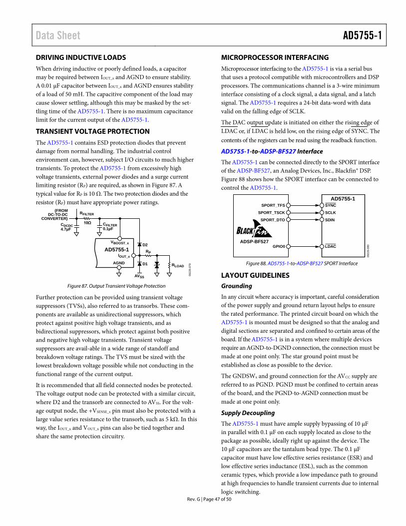
Data Sheet AD5755-1
Rev. G | Page 47 of 50
DRIVING INDUCTIVE LOADS When driving inductive or poorly defined loads, a capacitor may be required between IOUT_x and AGND to ensure stability. A 0.01 µF capacitor between IOUT_x and AGND ensures stability of a load of 50 mH. The capacitive component of the load may cause slower settling, although this may be masked by the set-tling time of the AD5755-1. There is no maximum capacitance limit for the current output of the AD5755-1.
TRANSIENT VOLTAGE PROTECTION The AD5755-1 contains ESD protection diodes that prevent damage from normal handling. The industrial control environment can, however, subject I/O circuits to much higher transients. To protect the AD5755-1 from excessively high voltage transients, external power diodes and a surge current limiting resistor (RP) are required, as shown in Figure 87. A typical value for RP is 10 Ω. The two protection diodes and the resistor (RP) must have appropriate power ratings.
RLOAD
RP
D2
D1
AVSS
AD5755-1VBOOST_x
IOUT_x
AGND
0922
6-07
9
RFILTER
CFILTER0.1µF
10Ω
(FROMDC-TO-DC
CONVERTER)CDCDC4.7µF
Figure 87. Output Transient Voltage Protection
Further protection can be provided using transient voltage suppressors (TVSs), also referred to as transorbs. These com-ponents are available as unidirectional suppressors, which protect against positive high voltage transients, and as bidirectional suppressors, which protect against both positive and negative high voltage transients. Transient voltage suppressors are avail-able in a wide range of standoff and breakdown voltage ratings. The TVS must be sized with the lowest breakdown voltage possible while not conducting in the functional range of the current output.
It is recommended that all field connected nodes be protected. The voltage output node can be protected with a similar circuit, where D2 and the transorb are connected to AVSS. For the volt-age output node, the +VSENSE_x pin must also be protected with a large value series resistance to the transorb, such as 5 kΩ. In this way, the IOUT_x and VOUT_x pins can also be tied together and share the same protection circuitry.
MICROPROCESSOR INTERFACING Microprocessor interfacing to the AD5755-1 is via a serial bus that uses a protocol compatible with microcontrollers and DSP processors. The communications channel is a 3-wire minimum interface consisting of a clock signal, a data signal, and a latch signal. The AD5755-1 requires a 24-bit data-word with data valid on the falling edge of SCLK.
The DAC output update is initiated on either the rising edge of LDAC or, if LDAC is held low, on the rising edge of SYNC. The contents of the registers can be read using the readback function.
AD5755-1-to-ADSP-BF527 Interface
The AD5755-1 can be connected directly to the SPORT interface of the ADSP-BF527, an Analog Devices, Inc., Blackfin® DSP. Figure 88 shows how the SPORT interface can be connected to control the AD5755-1.
0922
6-08
0
AD5755-1SYNC
SCLK
SDIN
LDAC
SPORT_TFS
SPORT_TSCK
SPORT_DTO
GPIO0ADSP-BF527
Figure 88. AD5755-1-to-ADSP-BF527 SPORT Interface
LAYOUT GUIDELINES Grounding
In any circuit where accuracy is important, careful consideration of the power supply and ground return layout helps to ensure the rated performance. The printed circuit board on which the AD5755-1 is mounted must be designed so that the analog and digital sections are separated and confined to certain areas of the board. If the AD5755-1 is in a system where multiple devices require an AGND-to-DGND connection, the connection must be made at one point only. The star ground point must be established as close as possible to the device.
The GNDSWx and ground connection for the AVCC supply are referred to as PGND. PGND must be confined to certain areas of the board, and the PGND-to-AGND connection must be made at one point only.
Supply Decoupling
The AD5755-1 must have ample supply bypassing of 10 µF in parallel with 0.1 µF on each supply located as close to the package as possible, ideally right up against the device. The 10 µF capacitors are the tantalum bead type. The 0.1 µF capacitor must have low effective series resistance (ESR) and low effective series inductance (ESL), such as the common ceramic types, which provide a low impedance path to ground at high frequencies to handle transient currents due to internal logic switching.
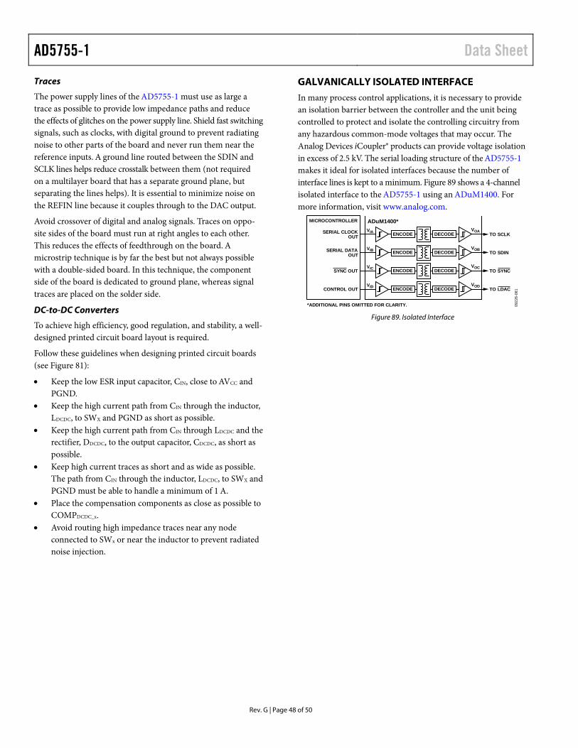
AD5755-1 Data Sheet
Rev. G | Page 48 of 50
Traces
The power supply lines of the AD5755-1 must use as large a trace as possible to provide low impedance paths and reduce the effects of glitches on the power supply line. Shield fast switching signals, such as clocks, with digital ground to prevent radiating noise to other parts of the board and never run them near the reference inputs. A ground line routed between the SDIN and SCLK lines helps reduce crosstalk between them (not required on a multilayer board that has a separate ground plane, but separating the lines helps). It is essential to minimize noise on the REFIN line because it couples through to the DAC output.
Avoid crossover of digital and analog signals. Traces on oppo-site sides of the board must run at right angles to each other. This reduces the effects of feedthrough on the board. A microstrip technique is by far the best but not always possible with a double-sided board. In this technique, the component side of the board is dedicated to ground plane, whereas signal traces are placed on the solder side.
DC-to-DC Converters
To achieve high efficiency, good regulation, and stability, a well-designed printed circuit board layout is required.
Follow these guidelines when designing printed circuit boards (see Figure 81):
• Keep the low ESR input capacitor, CIN, close to AVCC and PGND.
• Keep the high current path from CIN through the inductor, LDCDC, to SWX and PGND as short as possible.
• Keep the high current path from CIN through LDCDC and the rectifier, DDCDC, to the output capacitor, CDCDC, as short as possible.
• Keep high current traces as short and as wide as possible. The path from CIN through the inductor, LDCDC, to SWX and PGND must be able to handle a minimum of 1 A.
• Place the compensation components as close as possible to COMPDCDC_x.
• Avoid routing high impedance traces near any node connected to SWx or near the inductor to prevent radiated noise injection.
GALVANICALLY ISOLATED INTERFACE In many process control applications, it is necessary to provide an isolation barrier between the controller and the unit being controlled to protect and isolate the controlling circuitry from any hazardous common-mode voltages that may occur. The Analog Devices iCoupler® products can provide voltage isolation in excess of 2.5 kV. The serial loading structure of the AD5755-1 makes it ideal for isolated interfaces because the number of interface lines is kept to a minimum. Figure 89 shows a 4-channel isolated interface to the AD5755-1 using an ADuM1400. For more information, visit www.analog.com.
0922
6-08
1
VIASERIAL CLOCKOUT TO SCLK
VOAENCODE DECODE
VIBSERIAL DATAOUT TO SDIN
VOBENCODE DECODE
VICSYNC OUTVOC
ENCODE DECODE
VIDCONTROL OUTVODENCODE DECODE
MICROCONTROLLER ADuM1400*
*ADDITIONAL PINS OMITTED FOR CLARITY.
TO SYNC
TO LDAC
Figure 89. Isolated Interface

Data Sheet AD5755-1
Rev. G | Page 49 of 50
INDUSTRIAL HART CAPABLE ANALOG OUTPUT APPLICATION—SHARED VOUT_X AND IOUT_X PIN Many industrial control applications have requirements for accurately controlled current output signals, and the AD5755-1 is ideal for such applications. Figure 90 shows the AD5755-1 in a circuit design for a HART-enabled output module, specifically for use in an industrial control application in which both the voltage output and current output are available—one at a time—on one pin, thus reducing the number of screw connections required. There is no conflict with tying the two output pins together because only the voltage output or the current output can be enabled at any one time.
The design provides for a HART-enabled current output, with the HART capability provided by the AD5700/AD5700-1 HART modem, the industry’s lowest power and smallest footprint HART-compliant IC modem. For additional space-savings, the AD5700-1 offers a 0.5% precision internal oscillator. The HART_OUT signal from the AD5700 is attenuated and ac-coupled into the CHARTx pin of the AD5755-1. Such a configuration results in
the AD5700 HART modem output modulating the 4 mA to 20 mA analog current without affecting the dc level of the current. This circuit adheres to the HART physical layer specifications as defined by the HART Communication Foundation.
For transient overvoltage protection, a 24 V transient voltage suppressor (TVS) is placed on the IOUT/VOUT connection. For added protection, clamping diodes are connected from the IOUT_x/VOUT_x pin to the AVDD and AVSS power supply pins. A 5 kΩ current limiting resistor is also placed in series with the +VSENSE_x input. This is to limit the current to an acceptable level during a transient event. The recommended external band-pass filter for the AD5700 HART modem includes a 150 kΩ resistor, which limits current to a sufficiently low level to adhere to intrinsic safety requirements. In this case, the input has higher transient voltage protection and, therefore, does not require additional protection circuitry, even in the most demanding of industrial environments.
HART_OUT
GND
TXD
RXD
RTS
CD
VCC
AD5700/AD5700-1
0.1µF
ADC_IP
REF
GNDREFIN
RESET
AVDD SW (×4) VBOOST (×4)
CHART A
AD5755-1
DVDD
+15V +5V
10kΩ0.1µF
0.1µF
0.1µF
10µF
10µF
2.7V TO 5.5V
1.2MΩ
1.2MΩ
150kΩ300pF
150pF
1µF
MCU
D1
D2
RL500Ω
RP
VOUTA
+VSENSE_A
D3
AVSS
AVSSUARTINTERFACE
AVCC
IOUT B, C, D
IOUT A
CHART B, C, D
VOUT B, C, D
REFOUT
DGNDLDAC
SDOSDINSCLKSYNC
CLEAR
FAULT
ALERT
47nFC2
22nFC1
5kΩ
4mA TO 20mACURRENT LOOP
0922
6-08
9
Figure 90. AD5755-1 in HART Configuration
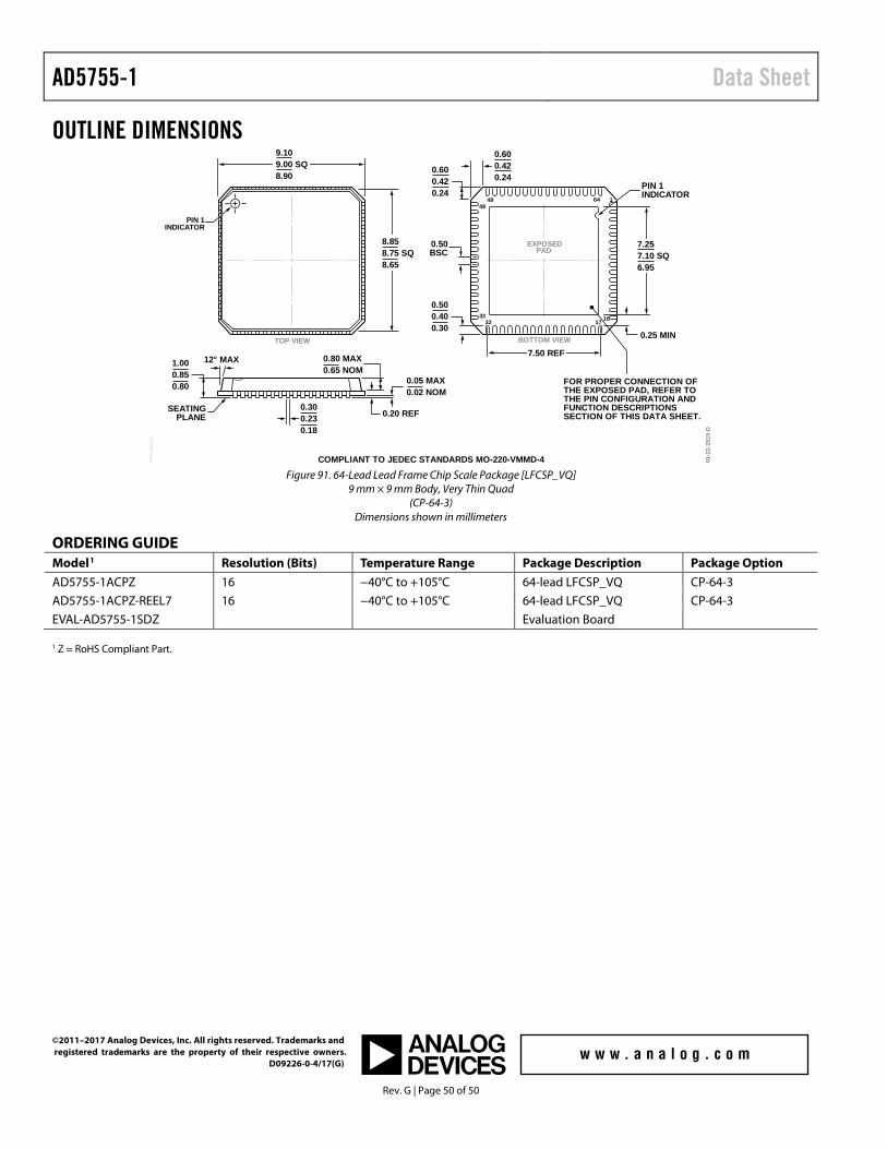
AD5755-1 Data Sheet
Rev. G | Page 50 of 50
OUTLINE DIMENSIONS
COMPLIANT TO JEDEC STANDARDS MO-220-VMMD-4
0.25 MIN
164
1617
4948
3233
0.500.400.30
0.50BSC
0.20 REF
12° MAX 0.80 MAX0.65 NOM
1.000.850.80
7.50 REF
0.05 MAX0.02 NOM
SEATINGPLANE
PIN 1INDICATOR
7.257.10 SQ6.95
PIN 1INDICATOR
0.300.230.18
FOR PROPER CONNECTION OFTHE EXPOSED PAD, REFER TOTHE PIN CONFIGURATION ANDFUNCTION DESCRIPTIONSSECTION OF THIS DATA SHEET.
TOP VIEW
EXPOSEDPAD
BOTTOM VIEW
9.109.00 SQ8.90
8.858.75 SQ8.65
01-2
2-20
15-D
0.600.420.24
0.600.420.24
PKG
-001
152
Figure 91. 64-Lead Lead Frame Chip Scale Package [LFCSP_VQ]
9 mm × 9 mm Body, Very Thin Quad (CP-64-3)
Dimensions shown in millimeters
ORDERING GUIDE Model1 Resolution (Bits) Temperature Range Package Description Package Option AD5755-1ACPZ 16 −40°C to +105°C 64-lead LFCSP_VQ CP-64-3 AD5755-1ACPZ-REEL7 16 −40°C to +105°C 64-lead LFCSP_VQ CP-64-3 EVAL-AD5755-1SDZ Evaluation Board 1 Z = RoHS Compliant Part.
©2011–2017 Analog Devices, Inc. All rights reserved. Trademarks and registered trademarks are the property of their respective owners. D09226-0-4/17(G)


![3 Two Ways to Measure Temperature Feature Simplicity ...€¦ · editor@analog.com or to Dan Sheingold, Editor [dan.sheingold@analog.com] or Scott Wayne, Publisher and Managing ...](https://static.fdocuments.us/doc/165x107/5e9fb3e69cfe7d3b494cce9e/3-two-ways-to-measure-temperature-feature-simplicity-editor-or-to-dan-sheingold.jpg)


![DC-to-DC Switching-Regulator Insights—Achieving Longer ... · By Sridhar Gurram [sridhar.gurram@analog.com] Oliver Brennan [oliver.brennan@analog.com] Tim Wilkerson [tim.wilkerson@analog.com]](https://static.fdocuments.us/doc/165x107/61219f3deb944c100772c8e6/dc-to-dc-switching-regulator-insightsaachieving-longer-by-sridhar-gurram-sridhargurram.jpg)