The dynamical-casimir-effect-in-superconducting-microwave-circuits

ABSTRACT
Title of dissertation: SUPERCONDUCTING LOGIC CIRCUITSOPERATING WITH RECIPROCALMAGNETIC FLUX QUANTA
Oliver Timothy Oberg,Doctor of Philosophy, 2011
Dissertation directed by: Professor Fred WellstoodDepartment of Physics
Complimentary Medal-Oxide Semiconductor (CMOS) technology is expected
to soon reach its fundamental limits of operation. The fundamental speed limit
of about 4 GHz has already effectively been sidestepped by parallelization. This
increases raw processing power but does nothing to improve power dissipation or
latency. One approach for increasing computing performance involves using super-
conducting digital logic circuits. In this thesis I describe a new kind of superconduct-
ing logic, invented by Quentin Herr at Northrop Grumman, which uses reciprocal
pairs of quantized single magnetic flux pulses to encode classical bits. In Recipro-
cal Quantum Logic (RQL) the data is encoded in integer units of the magnetic flux
quantum. RQL gates operate without the bias resistors of previous superconducting
logic families and dissipate several orders of magnitude less power.
I demonstrate the basic operation of key RQL gates (AndOr, AnotB, Set/Reset)
and show their self-resetting properties. Together, these gates form a universal logic
set and provide memory capabilities. Experiments measuring the bit error rate of

the AndOr gate extrapolated a minimum BER of 10−480 and a BER of 10−44 with
30% margins on flux biasing.
I describe an analytic timing model for RQL gates which demonstrates the
self-correcting timing features. From this model I derive equations for the timing
behavior and operating limits. Using this timing model I ran simulations to deter-
mine correction factions for more accurate predictions at higher frequencies. Using
these results, I also develop Very High Speed Integrated Circuit (VHSIC) Hardware
Description Language (VHDL) models to describe the combinational logic of RQL
gates.
To test the timing predictions of the timing model, I performed three experi-
ments on Nb/AlOx/Nb circuits at 4.2 K. The first measured the time of output. The
second measured the operating margins of the circuit. The third measured the max-
imum frequency of operation for RQL circuits. Together, these three experiments
showed quantitative agreement with the model for the timing output, qualitative
agreement with the limits of operation, and a projected speed limit of 50 GHz for
the Hypres 4.5 kA/cm2 process.
To power RQL circuits I describe a new design for power splitters and com-
biners which minimize standing waves. I describe a new kind of Wilkinson power
splitter which required numerical optimization but proved to be adequate. I exper-
imentally tested two new designs of the power splitter. Both showed less than 10%
variation in standing waves between power splitter and combiner, making it ade-
quate for RQL circuits. I also compared these results with the S-parameters of the
power network, which also indicated that the design was adequate for RQL circuits.

Finally, I tested an 8-bit Kogge-Stone architecture carry-look ahead adder
designed using VHDL models. The adder contained 815 Josephson junctions and
was fully functional at 6.21 GHz with a latency of 1.25 clock cycles. The adder
produced the correct logical output, had a measured optimal operating point within
8% of the optimal simulated operating point, and measured power margins of 1 dB.
It operated best at the designed clock amplitude of 0.88Ic and dissipated 0.570 mW
of power.

SUPERCONDUCTING LOGIC CIRCUITS OPERATING
WITH RECIPROCAL MAGNETICFLUX QUANTA
by
Oliver Timothy Oberg
Dissertation submitted to the Faculty of the Graduate School of theUniversity of Maryland, College Park in partial fulfillment
of the requirements for the degree ofDoctor of Philosophy
2011
Advisory Committee:Professor Frederick WellstoodProfessor Anna HerrProfessor Christopher LobbProfessor James AndersonDr. Benjamin PalmerProfessor Chris Davis

c© Copyright by
Oliver Timothy Oberg2011

Enjoy the little things in life,
for one day you may look back
and realize they were the big things.
- Robert Brault
ii

Acknowledgments
I have had a harder time properly giving thanks to the many people who made
this thesis possible than writing the whole rest of the thesis. Instead, I will try to
give acknowledgements as best I can in as short a space as possible, and trust that
those whom I may not have explicitly mentioned know they have more gratitude
than I can properly express.
First and foremost I’d like to thank Dr. Anna Herr, my research advisor first
at UMCP and then at Northrop Grumman. Her guidance and patience are the
foundation not only of my thesis but of my academic success so far. She has not
only given me fantastic research opportunities beyond any I expected to see in
graduate school but also taken a personal interest in my work and education. Even
at the busiest times she never failed to help me through a problem and I never had
to wait in idle frustration.
I also owe a great amount of appreciation to my academic advisor, Professor
Fred Wellstood at UMCP. He was willing to step in for me at the university to take
care of all University-related issues, and went above and beyond helping me review
and edit this thesis. His input has been both quite helpful and educational.
Dr. Quentin Herr at Northrop Grumman has been as much a mentor to me
as Anna or Fred. He has worked with me daily for almost three years and has been
instrumental in my understanding of superconductivity and microwave physics. This
thesis would not have been possible without his support, patience, and guidance.
There are many other individuals who have not only helped me greatly as
iii

a graduate student but have contributed their ideas and work efforts to the work
in this thesis. At Northrop Grumman, John Fusco has been pivotal in setting
up my graduate studies here. Stephen Van Campen has likewise been a fantastic
supporter in management without whom very little could have been accomplished.
Dr. James Baumgartner and Dr. Aaron Pesetski have been fantastically helpful and
supportive, always happy to explain concepts, provide feedback, and share a joke.
Dr. Ofer Naaman has been part of the same work efforts as I have and has always
been willing to help bridge the gaps in my understanding of microwave behavior and
superconductivity. Steven Shauck has been a wonderful tutor to me in all things
VHDL. He’s probably forgotten more about VHDL than I will ever know, but has
always been happy to find time in his very busy schedule to teach me about VHDL.
Alex Ioanniadis, who has since gone off to graduate school himself, was a fantastic
lab partner and experimentalist who taught me much of what I know about running
experiments. Donald Miller has been a constant resource of knowledge and wisdom,
always ready to help me hash out new and odd ideas and nitpick the details of old
ideas.
Many people have contributed directly to the results in this thesis. Quentin
Herr and Alex Ioanniadis performed the measurements shown in Figures 2.18 and
2.19. Ofer Naaman performed the numerical optimization of the design shown in
Figure 4.10 and made the CAD layout of the same device as seen in Figure 4.17.
Pavel Borodulin at Northrop Grumman supplied the analysis of the probe shown
in Figure C.2. Steven Shauck supplied the final design of the adder of Chapter 6.
Dr. John Pryzbysz at Northrop Grumman supplied the idea of using the spectrum
iv

analyzer to measure the side-band power of the CLA.
Although the bulk of my research was done at Northrop Grumman in Balti-
more, most of my education was done at College Park, where there are a number
of people I have to thank for their friendship, support, and camaraderie. I have
to thank Dr. Rupert Lewis — now also at Northrop Grumman — and Dr. Gus
Vlahacos for their kindness and support while I was starting my stint as a research
assistant. Many thanks to Professor Ellen Williams for years of guidance, listening
when others were busy or away.
I can not in good conscience fail to mention the handful of people outside of
work, and outside of the university who gave me emotional support and friendship.
I am lucky to have friends in almost every of the 50 states and in more countries
than I can remember off the top of my head. But a special few never wavered
from complete and permanent support in all parts of life, and without them my life
couldn’t have moved forward let alone would I have been able write this thesis.
v

Table of Contents
List of Tables viii
List of Figures ix
List of Abbreviations xii
1 Introduction to Superconductivity and Josephson Junctions 11.1 Overview . . . . . . . . . . . . . . . . . . . . . . . . . . . . . . . . . . 11.2 Superconductivity . . . . . . . . . . . . . . . . . . . . . . . . . . . . . 21.3 Josephson Junctions . . . . . . . . . . . . . . . . . . . . . . . . . . . 151.4 Superconducting Interferometers . . . . . . . . . . . . . . . . . . . . . 271.5 Introduction to Superconducting Digital Logic . . . . . . . . . . . . . 37
2 Reciprocal Quantum Logic 412.1 Introduction . . . . . . . . . . . . . . . . . . . . . . . . . . . . . . . . 412.2 Josephson Transmission Line . . . . . . . . . . . . . . . . . . . . . . . 422.3 Logic Gates . . . . . . . . . . . . . . . . . . . . . . . . . . . . . . . . 492.4 Composite Logic Gates . . . . . . . . . . . . . . . . . . . . . . . . . . 562.5 Fabrication and Equipment . . . . . . . . . . . . . . . . . . . . . . . 592.6 Experimental Verification . . . . . . . . . . . . . . . . . . . . . . . . 692.7 Summary . . . . . . . . . . . . . . . . . . . . . . . . . . . . . . . . . 82
3 Combinational Gates 833.1 Introduction . . . . . . . . . . . . . . . . . . . . . . . . . . . . . . . . 833.2 Junction Switching Time under AC Bias Current . . . . . . . . . . . 843.3 Timing Extraction from Simulation . . . . . . . . . . . . . . . . . . . 953.4 VHDL Models for RQL Gates . . . . . . . . . . . . . . . . . . . . . . 109
4 Power Network Design 1214.1 Introduction . . . . . . . . . . . . . . . . . . . . . . . . . . . . . . . . 1214.2 Circuit Design . . . . . . . . . . . . . . . . . . . . . . . . . . . . . . . 1234.3 Standalone Test . . . . . . . . . . . . . . . . . . . . . . . . . . . . . . 1434.4 Test with RQL Circuits . . . . . . . . . . . . . . . . . . . . . . . . . . 1554.5 Conclusions . . . . . . . . . . . . . . . . . . . . . . . . . . . . . . . . 161
5 Experimental Verification of RQL Timing Parameters 1635.1 Introduction . . . . . . . . . . . . . . . . . . . . . . . . . . . . . . . . 1635.2 Circuits and Simulation for Experiments 1, 2, 3 . . . . . . . . . . . . 1665.3 Experimental Setup . . . . . . . . . . . . . . . . . . . . . . . . . . . . 1745.4 Data and Analysis . . . . . . . . . . . . . . . . . . . . . . . . . . . . 1775.5 Conclusions . . . . . . . . . . . . . . . . . . . . . . . . . . . . . . . . 189
vi

6 Carry-Look Ahead Adder Experiment 1916.1 Introduction . . . . . . . . . . . . . . . . . . . . . . . . . . . . . . . . 1916.2 Circuit Design . . . . . . . . . . . . . . . . . . . . . . . . . . . . . . . 1916.3 Experimental Setup . . . . . . . . . . . . . . . . . . . . . . . . . . . . 1996.4 Experimental Results . . . . . . . . . . . . . . . . . . . . . . . . . . . 2016.5 Conclusions . . . . . . . . . . . . . . . . . . . . . . . . . . . . . . . . 216
7 Summary and Conclusions 2197.1 Summary . . . . . . . . . . . . . . . . . . . . . . . . . . . . . . . . . 2197.2 Conclusions and Future Work . . . . . . . . . . . . . . . . . . . . . . 2217.3 Final Words . . . . . . . . . . . . . . . . . . . . . . . . . . . . . . . . 224
Appendices 227
A Numerical Solution of the Sine-Gordon Equation 227
B Parameters for fits 229B.1 Timing Extraction Results for the JTL . . . . . . . . . . . . . . . . . 229B.2 Comparison of Threshold Values in Timing Extraction . . . . . . . . 233B.3 Simulation File for Timing Extraction . . . . . . . . . . . . . . . . . . 234
C Wilkinson Power Splitter Response Parameters 263C.1 Derivation of Impedance Values . . . . . . . . . . . . . . . . . . . . . 263C.2 HPI Probe Internal Reflections . . . . . . . . . . . . . . . . . . . . . 267C.3 Netlist for simulation of S-Parameters . . . . . . . . . . . . . . . . . . 268
D Fitting Functions for Race Circuit Experiments 272D.1 Two-Output Fitting Code . . . . . . . . . . . . . . . . . . . . . . . . 272D.2 Fit to Experiment 2 Data . . . . . . . . . . . . . . . . . . . . . . . . 276D.3 And-Output Fitting Code for gnuplot . . . . . . . . . . . . . . . . . . 277D.4 Calculation of Depressed IcRN Product . . . . . . . . . . . . . . . . . 282
E Hypres Fabrication Summary 284
F Spice Netlist of CLA 287
Bibliography 319
vii

List of Tables
2.1 Universal Logic Test . . . . . . . . . . . . . . . . . . . . . . . . . . . 72
3.1 Comparison of different Jc, IcRN and switching time t0 . . . . . . . . 873.2 Timing Fit Results . . . . . . . . . . . . . . . . . . . . . . . . . . . . 1023.3 Global VHDL Quantities . . . . . . . . . . . . . . . . . . . . . . . . . 1113.4 Truth table for AndOr and AnotB in VHDL . . . . . . . . . . . . . . 1153.5 Truth table for Set/Reset in VHDL . . . . . . . . . . . . . . . . . . . 1173.6 Truth table for a JTL in VHDL . . . . . . . . . . . . . . . . . . . . . 119
4.1 Impedance values for the Wilkinson splitter stages . . . . . . . . . . . 1284.2 Resistance values in Wilkinson power splitter . . . . . . . . . . . . . . 1324.3 Chip resonance lengths for frequencies f of interest . . . . . . . . . . 161
5.1 Operational bias conditions for N22TE . . . . . . . . . . . . . . . . . 1775.2 Fitting parameters of two-output circuit data . . . . . . . . . . . . . 1815.3 Summary of measurements of Pin and Vp−p in N22TE . . . . . . . . . 1855.4 Analysis of the long, deep shift register from N22TE . . . . . . . . . . 189
6.1 Expected CLA output pattern for two cyclic input sequences . . . . . 2036.2 Power Measurement Calculations . . . . . . . . . . . . . . . . . . . . 217
B.1 Extracted JTL Timing Parameters . . . . . . . . . . . . . . . . . . . 230B.2 Extraction of JTL Timing Parameters (polynomial fit) . . . . . . . . 231B.3 Extraction of AndOr OR output timing parameters . . . . . . . . . . 232
D.1 Fitting parameters of and-output circuit data . . . . . . . . . . . . . 277D.2 Alternative switching time calculation . . . . . . . . . . . . . . . . . . 283
E.1 Hypres fabrication design specifications . . . . . . . . . . . . . . . . . 286
viii

List of Figures
1.1 Green’s Functions Ip and Iq for Josephson Junction at T = 0 . . . . . 141.2 Superconductor-Insulator-Superconductor tunneling I-V Curve . . . . 151.3 Superconductor-Insulator-Superconductor Tunneling . . . . . . . . . . 181.4 Equivalent electrical circuit of a Josephson Junction in the RSJ model 201.5 Phase Diagram of Josephson Junction . . . . . . . . . . . . . . . . . . 231.6 Josephson junction potential energy . . . . . . . . . . . . . . . . . . . 251.7 Voltage vs time dynamics of overbiased junction . . . . . . . . . . . . 281.8 I-V curve of current driven junctions . . . . . . . . . . . . . . . . . . 291.9 Single-junction interferometer . . . . . . . . . . . . . . . . . . . . . . 301.10 Single-junction interferometer . . . . . . . . . . . . . . . . . . . . . . 321.11 Josephson Transmission Line . . . . . . . . . . . . . . . . . . . . . . . 351.12 Phase behavior of junction in JTL . . . . . . . . . . . . . . . . . . . . 36
2.1 Basic RQL Interconnect Element . . . . . . . . . . . . . . . . . . . . 432.2 Josephson transmission line and SFQ launch circuit diagram . . . . . 442.3 Data propagation in an RQL 4-phase clock transmission line . . . . . 472.4 Deep Pipeline JTL . . . . . . . . . . . . . . . . . . . . . . . . . . . . 482.5 RQL Logic Gates . . . . . . . . . . . . . . . . . . . . . . . . . . . . . 502.6 Set/Reset Unit . . . . . . . . . . . . . . . . . . . . . . . . . . . . . . 542.7 RQL Exclusive-OR Gate . . . . . . . . . . . . . . . . . . . . . . . . . 562.8 Non-Destructive Read-Out Gate . . . . . . . . . . . . . . . . . . . . . 582.9 RQL Clock Line Transformer Layout . . . . . . . . . . . . . . . . . . 602.10 RQL Clock Line Transformer with DC Bias . . . . . . . . . . . . . . 622.11 Schematic of test probe . . . . . . . . . . . . . . . . . . . . . . . . . . 642.12 Layout of Monrovia 20 RQL chip . . . . . . . . . . . . . . . . . . . . 652.13 Monrovia 20 logic chip . . . . . . . . . . . . . . . . . . . . . . . . . . 672.14 Experimental setup for timing experiments . . . . . . . . . . . . . . . 682.15 Oscilloscope output . . . . . . . . . . . . . . . . . . . . . . . . . . . . 702.16 Logic Test of Basic RQL Gates . . . . . . . . . . . . . . . . . . . . . 742.17 Power schematic for RQL . . . . . . . . . . . . . . . . . . . . . . . . 762.18 Power Dissipation Measurements . . . . . . . . . . . . . . . . . . . . 792.19 Bit Error Rate . . . . . . . . . . . . . . . . . . . . . . . . . . . . . . 81
3.1 Junction phase delay versus starting junction phase θ . . . . . . . . . 883.2 Self-correcting timing mechanism of RQL . . . . . . . . . . . . . . . . 903.3 Relationship between input time on consecutive phases . . . . . . . . 923.4 Switching delay ν versus input phase for different clock frequencies . 943.5 Phases of two sequential junctions during switching . . . . . . . . . . 983.6 Data path through AndOr gate . . . . . . . . . . . . . . . . . . . . . 993.7 Circuits used to extract RQL timing results from spice simulations . . 1003.8 Fit of delay equation to simulated switching times . . . . . . . . . . . 1043.9 Simulated delay versus input phase . . . . . . . . . . . . . . . . . . . 1063.10 Comparison of Extracted Timing Curves . . . . . . . . . . . . . . . . 107
ix
3.11 Simulated timing data for the JTL at 13 GHz . . . . . . . . . . . . . 1083.12 Timing model for RQL clock . . . . . . . . . . . . . . . . . . . . . . . 1103.13 Combinational logic of RQL gates . . . . . . . . . . . . . . . . . . . . 1143.14 AndOr gate VHDL code . . . . . . . . . . . . . . . . . . . . . . . . . 1163.15 Combinational behavior of the JTL in VHDL . . . . . . . . . . . . . 118
4.1 Wilkinson Power Splitter . . . . . . . . . . . . . . . . . . . . . . . . . 1224.2 Schematic of the Wilkinson power splitter (1221 configuration) . . . . 1254.3 Even and Odd mode analysis of the Wilkinson Power Splitter . . . . 1264.4 Wilkinson 1221 Simulated Reflection Parameters . . . . . . . . . . . . 1294.5 Circuit schematic for Wilkinson 4440 configuration . . . . . . . . . . 1304.6 Circuit schematic for WPS2220 . . . . . . . . . . . . . . . . . . . . . 1304.7 Geometric versus max flat power splitter reflections . . . . . . . . . . 1314.8 Geometric power splitter isolation . . . . . . . . . . . . . . . . . . . . 1334.9 Isolation parameter measurement . . . . . . . . . . . . . . . . . . . . 1344.10 Circuit schematic for N23PS . . . . . . . . . . . . . . . . . . . . . . . 1354.11 Wilkinson 3111 Simulated S-Parameters . . . . . . . . . . . . . . . . 1364.12 Block diagram for measuring standing currents . . . . . . . . . . . . . 1384.13 Simulated standing wave currents . . . . . . . . . . . . . . . . . . . . 1394.14 Standing Waves in Wilkinson 3111 Power Network . . . . . . . . . . . 1424.15 Experimental setup for measurement of S-parameters . . . . . . . . . 1434.16 M20PS even mode test . . . . . . . . . . . . . . . . . . . . . . . . . . 1454.17 Microphotograph of Norwalk 23 . . . . . . . . . . . . . . . . . . . . . 1474.18 Measured parameters of geometric power splitter . . . . . . . . . . . 1484.19 Simulated reflection for the N23PS circuit . . . . . . . . . . . . . . . 1504.20 Measured S-parameters on N21CLA Wilkinson power splitter . . . . . 1524.21 S-parameters from ADS for N23PS . . . . . . . . . . . . . . . . . . . 1544.22 Odd mode test block diagram for N23PS . . . . . . . . . . . . . . . . 1564.23 Wilkinson-powered RQL circuit measurements of N23PS . . . . . . . 160
5.1 Microphotograph of N22TE . . . . . . . . . . . . . . . . . . . . . . . 1645.2 Block diagram and layout of N22TE . . . . . . . . . . . . . . . . . . 1675.3 Input and output phases versus time for the two-output race circuit . 1685.4 Two-output race circuit timing predictions . . . . . . . . . . . . . . . 1705.5 Operational space of N22TE . . . . . . . . . . . . . . . . . . . . . . . 1715.6 Long, deep pipeline shift register . . . . . . . . . . . . . . . . . . . . 1745.7 Experimental setup for timing experiments . . . . . . . . . . . . . . . 1755.8 Two-output race circuit measured data . . . . . . . . . . . . . . . . . 1795.9 And-output race circuit data . . . . . . . . . . . . . . . . . . . . . . . 1825.10 Multi-Phase Shift Register Amplitude Margins . . . . . . . . . . . . . 187
6.1 Photo of N21CLA . . . . . . . . . . . . . . . . . . . . . . . . . . . . . 1926.2 Carry-Look Ahead elements . . . . . . . . . . . . . . . . . . . . . . . 1946.3 Generic Kogge-Stone CLA Architecture . . . . . . . . . . . . . . . . . 1966.4 Final Carry-Look Ahead Adder design . . . . . . . . . . . . . . . . . 198
x

6.5 Block diagram of experimental setup for N21CLA . . . . . . . . . . . 2006.6 Shift register input for CLA . . . . . . . . . . . . . . . . . . . . . . . 2026.7 Measured CLA Output . . . . . . . . . . . . . . . . . . . . . . . . . . 2056.8 Power margins for CLA . . . . . . . . . . . . . . . . . . . . . . . . . 2086.9 Measured power spectrum of Carry-Look Ahead Adder . . . . . . . . 2116.10 Modulation of Clock Signal by RQL Gate Operation . . . . . . . . . 212
B.1 Comparison of Threshold Values . . . . . . . . . . . . . . . . . . . . . 234
C.1 Simulated Probe PCB Losses . . . . . . . . . . . . . . . . . . . . . . 267C.2 S-Parameter Test Circuits . . . . . . . . . . . . . . . . . . . . . . . . 268
D.1 Curve fitting to Experiment 2 . . . . . . . . . . . . . . . . . . . . . . 277
xi

List of Abbreviations
ADS Advanced Design System 2009 softwareBCS Bardeen-Cooper-SchriefferBER Bit Error RateCLA Carry Look AheadCMOS Complimentary metal-oxide-semiconductorGHz GigahertzHPD High Precision DevicesIREAP Institute for Research in Electronics and Applied PhysicsJJ Josephson JunctionJTL Josephson Transmission LineNSA National Security AgencyNRZ Non-Return to ZeroPCB printed circuit boardps picosecondRQL Reciprocal Quantum LogicRSFQ Resistive Single Flux QuantumRSJ Resistively Shunted JunctionRZ Return to ZeroSFQ Single Flux QuantumSIS Superconductor-Insulator-SuperconductorSNS Superconductor-Normal Metal-SuperconductorSQUID Superconducting QUantum Interference Devicestd ulogic Synopsys extension to IEEE 1164, a VHDL classVHDL VHSIC Hardware Description LanguageVHSIC Very High Speed Integrated CircuitVLSI Very Large Scale Integrationθ Clock phase (θ = ω t in most cases)ν(θ) Analytic Timing Model equationφ Phase across Josephson junction
List of Samples
M20LT Monrovia 20 Logic TestM20SR Monrovia 20 Shift RegisterM20PS Monrovia 20 Power SplitterN23PS Norwalk 23 Power SplitterN22TE Norwalk 22 Timing ExperimentN21CLA Norwalk 21 Carry Look Ahead Adder
xii

Chapter 1
Introduction to Superconductivity and Josephson Junctions
1.1 Overview
Nearly 200 years passed between Franklin’s discovery of electricity and the de-
velopment of the first electronic computer [1, 2]. Superconductivity was discovered
in 1911 by Heike Kamerlingh Onnes [3] and only began to impact computing about
50 years later [4]. In 1962 Brian David Josephson postulated the Josephson effect,
which would lead to the invention of the dc SQUID two years later [5]. By the mid-
1980s IBM terminated a major effort to build a computer using superconductivity.
Shortly thereafter Josephson junctions began being considered for reversible com-
putation [6] and used in Resistive Single Flux Quantum digital circuits [4]. Now,
one century after the discovery of superconductivity, contemporary semiconductor-
based computation seems to be approaching a fundamental limit [7] and this raises
the possibility that a new generation of computers based on superconductivity and
Josephson junctions may arise to push technology forward [8].
One technology potentially capable of pushing computation forward is Recip-
rocal Quantum Logic (RQL), the subject of my research over the past few years. The
goal of this research was to demonstrate the feasibility of using RQL for very high
speed and very low power computation. This thesis has three main parts. First, I
provide a basic overview of superconductivity and Josephson junctions (Chapter 1).
1

This overview is far from exhaustive but serves to highlight aspects that are most
important to the subsequent discussion of RQL. The first part concludes with an
introduction to RQL (Chapter 2), which is where my own work begins. Next, in the
second part, I describe my research into the behavior of junctions using high-level
simulations in Very High Speed Integrated Circuit Hardware Description Language
(VHDL). In Chapter 3, I derive an analytic model for the timing behavior of Joseph-
son junctions in RQL circuits. After I verify this model in simulations, I proceed
to cast RQL into the industry-standard VHDL. Chapter 4 is a departure from the
previous topics and describes the development of a new power network for RQL,
but together chapters 2–4 provide the basis for design of functioning circuits. In the
third part, I describe my experiments testing the timing behavior (Chapter 5) and
a fully functioning 8-bit adder (Chapter 6). Finally, in Chapter 7, I conclude with
a brief summary of my main results and make some suggestions for future work.
1.2 Superconductivity
Following the discovery of superconductivity in 1911 many attempts were made
to understand the phenomenon. In the Drude model of conduction in normal metals
current density is proportional to the average velocity of electrons [9], which accel-
erate under an electric field over a distance l until colliding with defects and slowing
down. A stable current is reached when the average deceleration due to collisions
matches the acceleration due to the electric field. In the limit l → ∞ infinite con-
ductivity would result. However, in the 1930s it was found a superconductor is not
2

merely a metal with infinite conductivity. Superconductors exhibit new behavior
that ultimately required new physics to be understood.
1.2.1 London Equations
Around the time superconductivity was being discovered, quantum mechanics
was being developed. In quantum mechanics the canonical momentum of a particle
in a magnetic field is given by
~p = m~v + qe ~A, (1.1)
where m is the particle’s mass, q is its charge, e is defined as the magnitude of the
charge of an electron (+1.609×10⁻¹⁹ C), and ~v and ~A are the velocity and magnetic
vector potential. If one assumes that in the ground state of a system the (local)
average 〈~p〉 = 0 then the current density Js can be expressed as
~Js = nse〈~vs〉 = −nse2
m~A = −
~A
Λ. (1.2)
Here the s-subscript refers to superconducting currents and electrons and Λ =
m/nse2. We can also define Λ = λ2; the meaning of λ will become clearer, but
for now we note that it has dimensions of length. Taking the time derivative and
then the curl of (1.2), one can show that this leads to the London equations [9, 10]
for the electric field ~E = −∂ ~A/∂t and magnetic field ~H = ∇× ~A
~E =∂
∂t(Λ ~Js), (1.3)
~H = −∇× (Λ ~Js). (1.4)
3

Finally, using Maxwell’s equation ∇× ~H = ~Js on (1.4) gives
∇2 ~H =~H
λ2, (1.5)
which implies that λ is the characteristic length scale for the penetration of magnetic
field into a bulk superconductor.
Equations (1.3) – (1.5) were first obtained by Fritz and Heinz London in 1935
[10]. The original London equations were phenomenological and Λ was simply a
fitting parameter. Two insightful results come from this very cursory derivation.
Equation (1.3) implies that the current increases in time for a static electric field.
Meanwhile, (1.4) implies that magnetic fields are expelled from the interior of super-
conductors within a characteristic length λ. Note also that the value of ns is limited
on the upper end by the total number of charges in the metal. It can be seen from
energy considerations that (1.3) and (1.5) imply an upper limit on the current den-
sity ~Js. In addition, in a wire carrying a current, the magnetic field generated by
the current will be constrained to a depth λ in the wire. If the current gets too
large, the magnetic forces from the current would drive charge into the interior of
the wire, destroying the superconductivity. These rough phenomenological consider-
ations reveal some of the major features of superconductivity. However, the insight
they provide of the superconducting state is limited. For a fuller understanding, I
turn to the theory developed by Bardeen, Cooper, and Schrieffer in 1957 [11].
I have three goals for this section. First, I show that the superconducting
state exists at any temperature below the transition temperature. Second, I show
that quasiparticles in a superconductor have an energy that is at least as large as
4

the superconducting energy gap. Finally, the third and most important point is to
develop an understanding of the I-V curve of a Josephson Tunnel junction, as this
will be the basis for much of the rest of the thesis.
1.2.2 BCS Theory
In superconducting materials and at finite temperatures, ordinary unpaired
electrons are present as well as superconducting Cooper pairs [9]. Unpaired elec-
trons yield a normal current component and follow Fermi-Dirac statistics. Two
unpaired electrons will generally not have identical energies (with the exception of
spin pairs) and consequently their quantum mechanical phase will change at dif-
ferent rates. In contrast, Cooper pairs follow Bose-Einstein statistics and can have
identical energies and phase. In conventional BCS superconductors, Cooper pairs
are formed by the interaction of electrons mediated though the exchange of phonons.
Individual Cooper pairs are much larger than the mean spacing between pairs [9]
and the pairs maintain phase coherence amongst each other by the large amount of
overlap between their wave functions [9].
1.2.2.1 Cooper Pairs
Since electrons are charged they exert a Coulomb force on the semi-stationary
nuclei in a metal. This force can scatter the electron and perturb nuclei from their
equilibrium positions. The perturbations of positive nuclei by a scattered electron
can attract other electrons, thus resulting in a net attractive potential V between
5

two electrons despite the presence of electron-electron Coulomb repulsion. In a
superconductor this attraction leads to electrons pairing up. The general wave
function for a Cooper pair is
ψ0(~r1, ~r2) =∑
~k
g~k ei~k·~r1 e−i~k·~r2χ1χ2, (1.6)
where ~r1 and ~r2 are the positions of the first and second electron, respectively, g~k
is the weighing factor of the orbital wave function, ~k is the wave vector, and χ1
and χ2 are spin functions for the first and second electron, respectively. This wave
function can be recast into a form that is explicitly anti-symmetric in ~r1 and ~r2 by
considering the distance between a pair ~r1 − ~r2. We can write in general
ψ0(~r1 − ~r2) =
∑
~k>~kF
g~k cos~k · (~r1 − ~r2)
σsinglet12 (1.7)
for the singlet state in conventional BCS theory [11]. The sum in (1.7) is only over
wave vectors that have lengths greater than the Fermi wave vector, for reasons which
will become apparent shortly. σsinglet12 is the spin part of the singlet wave function
and it is anti-symmetric under exchange of the electrons.
Inserting (1.7) into Schrodinger’s equation gives a relationship between the
energy E and the interaction potential V [9]:
1
V=∑
~k>~kF
1
2ǫ~k − E(1.8)
where ǫ~k = h2k2/2m. Equation (1.8) can be evaluated as an integral from the Fermi
energy EF to a higher energy EF + hωc. One finds
1
V N(0)=
∫ EF+hωc
EF
dǫ
2ǫ− E=
1
2ln
2EF −E + 2hωc
2EF −E, (1.9)
6
where N(0) is the density of electron states at the Fermi level. In the weak-coupling
approximation V N(0) ≪ 1 one finds
E ≈ 2EF − 2hωc e−2/V N(0). (1.10)
This result shows that the energy of a pair is reduced by the interaction in a non-
perturbative manner and bound states (pairs) can exist no matter how small V
becomes.
1.2.2.2 Ground State
To get further understanding of the behavior of a superconductor we apply
second quantization [9]. Let |F 〉 be the state of a metal in which all the electron
states below the Fermi surface are occupied. Then the wave function for the state
ψ0 of a superconductor becomes
|ψ0〉 =∑
~k>~kF
g~k c∗~k ↑ c
∗−~k ↓ |F 〉 (1.11)
where c∗~k σand c~k σ are the creation and annihilation operators for a pair with mo-
mentum ~k and spin σ and the g~k are weighing factors for the pairs, with the anti-
commutation relations
c~k σ, c∗~k′ σ′
= δkk′δσσ′ andc~k σ, c~k′ σ′
= 0. The number of
electrons which wave vector k and spin σ is then given by the operator nkσ = c∗kσckσ
which gives unity when operating on a filled state and zero when operating on an
unoccupied state.
In a macroscopic superconductor at sufficiently low temperature the fluctua-
tions about the ground state will be small and Bardeen, Cooper, and Schrieffer were
7

able to apply a mean-field approach [9]. They wrote the ground state as a product
of superposition states with differing momenta:
|ψG〉 =∏
~k1,...,~kM
(
u~k + v~k c∗~k ↑ c
∗−~k ↓
)
|ψ0〉 , (1.12)
with∣∣v~k∣∣2+∣∣u~k∣∣2 = 1.
∣∣v~k∣∣2 is the probability of the state
(
~k ↑,−~k ↓)
being occupied
and∣∣u~k∣∣2 is the probability of it being empty. We can learn a bit about the ground
state ψG if we assume v~k and u~k differ by a set phase. With this assumption, we
can rewrite (1.12) as
|ψG〉 =∏
~k1,...,~kM
(∣∣u~k∣∣ +∣∣v~k∣∣ eiϕ c∗~k ↑ c
∗−~k ↓
)
|ψ0〉 . (1.13)
The phase ϕ turns out to be the order parameter of the superconductor, and it
obeys an uncertainty relationship with the number of pairs N [9]:
∆N∆ϕ ≥ 1. (1.14)
1.2.2.3 Pairing Hamiltonian
To arrive at (1.12) for the state φ0, Bardeen, Cooper, and Schrieffer wrote a
simplified Hamiltonian H that included a pairing-interaction term
H =∑
~kσ
ǫk n~kσ +∑
~k~k′
V~k~k′ c∗~k↑ c
∗−~k↓ c−~k′↓ c~k′↑. (1.15)
The first term is the energy ǫk of a Cooper pair with momentum k and spin σ. The
second term describes the energy gained by the annihilation of a Cooper pair con-
sisting of electrons with momentum ~k′ and the creation of a pair with momentum
~k, where V~k~k′ is the scattering matrix element. Interactions between electrons with
8

different momenta ~k do not play a role in BCS theory but may in other applica-
tions. The ground state (1.12) and Hamiltonian (1.15) can then be substituted into
Schrodinger’s equation. The ground state energy and g~k can be found by a canonical
transformation. Following Tinkham [9] we define b~k = 〈c−~k↓ c~k↑〉 and write
c−~k↓ c~k↑ = b~k +(
c−~k↓ c~k↑ − b~k
)
. (1.16)
The ideas is that the term in parentheses should be small. I can also define ∆~k =
−∑
~k′ V~k~k′ 〈c−~k↓ c~k↑〉 and ξ~k = ǫ~k − EF , neglecting terms that are quadratic in the
term in parentheses above. Then the Hamiltonian becomes [9]
H =∑
~kσ
ξ~k c∗~kσc~kσ −
∑
~k
(
∆~k c∗~k↑ c
∗−~k↓ +∆∗
~kc∗−~k↓ c
∗~k↑ −∆~k b
∗~k
)
(1.17)
This can be diagonalized if we define new creation operator η∗k and annihilation
operator γ~k from:
c~k = u∗~k γ~k + v~k η∗~k
(1.18)
c∗−~k= −v∗~k γ~k + u~k η
∗~k
(1.19)
where the v~k and u~k satisfy
∣∣v~k∣∣2=
1
2
(
1− ξ~kE~k
)
(1.20)
∣∣u~k∣∣2=
1
2
(
1 +ξ~kE~k
)
(1.21)
Finally (1.15) and (1.17) can be put in the form [9]:
H =∑
~k
(ξ~k − E~k +∆~k b
∗~k
)+∑
~k
E~k
(γ∗~kγ~k + η∗~kη~k
)(1.22)
9

This Hamiltonian has two terms. The first term is just the condensation energy
and is a constant. The second term accounts for the energy due to quasiparticles
with energy E~k =(
ξ2~k +∣∣∆~k
∣∣2)1/2
. ∆~k is the energy decrease when a Cooper pair
forms. A superconducting state will be stable if the energy decrease for a pair
forming is greater than that required to leave the Fermi surface. Once a pair is
formed, 2∆ is the energy necessary to break a pair into two quasiparticles.
1.2.2.4 Density of States
Quasiparticles behave much like electrons in a normal metal. The density of
states Ns(E) of the quasiparticles is related to the density of states of the electrons
in the normal metal Nn(ξ) by Ns(E)dE = Nn(ξ)dξ. For energies small compared to
the Fermi energy the number of normal electron states Nn(ξ) = N(0) can be taken
as constant [9]. One then finds:
Ns(E)
N(0)=
dξ
dE=
E/√E2 −∆2 if E > ∆
0 if E < ∆
(1.23)
The dependance of Ns on the quasiparticle energy E is directly manifest in
the tunneling behavior between superconductors. The quasiparticle current I that
flows between two superconductors with a voltage V between them can be written
10

as [9]:
I ≃ A
∫ +∞
−∞N1(E)N2(E + eV )(f(E)− f(E + eV )) dE
= A
∫ +∞
−∞
Ns1(E)
N1(0)
Ns1(E + eV )
N1(0)(f(E)− f(E + eV )) dE
= A
∫ +∞
−∞
|E|√
E2 −∆21
|E + eV |√
(E + eV )2 −∆22
(f(E)− f(E + eV )) dE, (1.24)
where f(E) is the Fermi function (probability that a quasiparticle state at energy
E is occupied) and A is a constant that depends on the junctions barrier and other
details such as temperature.
This integral (1.24) can be evaluated numerically or treated analytically for
T = 0. Instead, I consider an analysis of the IV curve by Likharev. To proceed,
first transform the phase ϕ(t) into its Fourier components W (ω) by using
eiϕ/2 = eiΦ/2
∫ +∞
−∞W (ω)eiωtdω
where the time derivative of Φ is related to the average voltage V by Φ = (2 e/h)V .
Barone et al. then define the supercurrent component IS(t) and normal current
component IN(t) as [4]
IS(t) = Im
(∫ +∞
−∞dω1
∫ +∞
−∞dω2W (ω1)W (ω2)Ip
(
ω2 +ωJ
2
)
ei(ω!+ω2)t+iΦ
)
, (1.25a)
IN(t) = Im
(∫ +∞
−∞dω1
∫ +∞
−∞dω2W (ω1)W
∗(ω2)Iq
(
ω2 +ωJ
2
)
ei(ω!+ω2)t
)
. (1.25b)
In turn, we define Ip and Iq as the Green’s functions for the superconducting elec-
trodes. These functions do not depend on the phase dynamics of the junction, only
11

the junction itself. They characterize the junction fully and are given by [4]
Ip(ω) =1
GN (2π2e)
∫ +∞
−∞dω1
∫ +∞
−∞dω2
(
tanhhω1
2kBT+ tanh
hω2
2kBT
)
(1.26a)
× Im (F1(ω1)) Im (F2(ω2))
ω1 + ω2 − w + j0,
Iq(ω) =1
GN (2π2e)
∫ +∞
−∞dω1
∫ +∞
−∞dω2
(
tanhhω1
2kBT+ tanh
hω2
2kBT
)
(1.26b)
× Im (G1(ω1)) Im (G2(ω2))
ω1 + ω2 − w + j0,
where the subscripts 1 and 2 refer to the left and right superconducting banks of
the junction. The functions F and G can be derived from BCS theory and are given
by [4]
F (ω) =π∆(T )
√
∆2(T )− h2(ω + j0)2, (1.27)
G(ω) =πhω
√
∆2(T )− h2(ω + j0)2. (1.28)
The term ω + j0 is real. The latter part of the expression is a remnant from the
complex analysis used to derive the expression and included here for clarity. Barone
and Paterno provide a detailed analysis including this term [6]. Substituting (1.27)
and (1.28) into (1.26a) and (1.26b) one finds relations for the real and imaginary
12

components of Ip and Iq. (See Fig. 1.1.)
Re Ip(ω) =∆(0)
eRN×
K(x) if x < 1
x−1K(x−1) if x > 1
(1.29a)
Im Ip(ω) =∆(0)
eRN×
0 if x < 1
x−1K(x′) if x > 1
(1.29b)
Re Iq(ω) = sign(ω)∆(0)
eRN×
K(x)− 2E(x) if x < 1
(2x− x−1K(x−1)− 2xE(x−1) if x > 1
(1.29c)
Im Iq(ω) = sign(ω)∆(0)
eRN×
0 if x < 1
2xE(x′)− x−1K(x′) if x > 1
(1.29d)
where E and K are complete elliptic integrals of the first and second kind, re-
spectively. I also define x = |ω|/ωg, the gap frequency ωg = 2∆(T )/h, and
x′ =√1− x−2. Equations (1.29a)–(1.29d) are true only for T = 0; at higher
temperatures Ip and Iq must be calculated numerically.
By evaluating these equations at arbitrary temperature T , we can find an
expression for Vc = IcRN for SIS junctions in terms of the gap energy ∆. Here Ic
is the critical current and RN is the normal resistance of the junction. Substituting
(1.27) and (1.28) into (1.26a) and (1.26b) one finds
Vc = IcRN =π
2 e∆(T ) tanh
∆(T )
2kBT(1.30)
for SIS junctions [4].
Figure 1.2 shows the average current I for a constant voltage V found from
13

-2
-1
0
1
2
3
4
0 0.4 0.8 1.2ω / ωg
Re Ip
0 0.4 0.8 1.2ω / ωg
Im Ip
0 0.4 0.8 1.2ω / ωg
Re Iq
0 0.4 0.8 1.2ω / ωg
Im Iq
Figure 1.1: Green’s Functions Ip and Iq for Josephson Junction atT = 0. Real and imaginary components of the Cooper pair and quasi-particle Green’s functions from (1.29a) – (1.29d) in superconductor-to-superconductor tunneling. Each components shows a clear transition atthe gap frequency ωc. Below this frequency Im Ip = 0 and Im Iq = 0; noquasiparticles tunnel through the barrier.
(1.29a) – (1.29d). Below Vc only a relatively small number of thermally excited
quasiparticles tunnel and the average current is low. Only past a critical voltage
Vc ≈ 2∆/e does current flow. Above Vc the current is similar to that of a non-
superconducting tunnel junction. This behavior is important for Josephson junc-
tion dynamics, which shall be the topic of the rest of this chapter. However, it is
important to note that it does not include supercurrent flow at V = 0. V = 0
supercurrent flow is considered in the next section.
14

0
0.2
0.4
0.6
0.8
1
1.2
0 0.2 0.4 0.6 0.8 1 1.2
Average
CurrentI/I
c
Voltage V/Vc
Figure 1.2: Superconductor-Superconductor Tunneling I-V Curve forV > 0. The time-averaged current from (1.24) is plotted at zero tem-perature (red). Blue curve shows the effects of non-zero temperature.Green curve shows linear resistive I-V relationship of the normal state.Below Vc a nearly negligible current of unpaired electrons flows in thesuperconducting state. Above this critical potential, Cooper pairs breakapart and the I-V curve becomes similar to the ohmic resistance curve.
1.3 Josephson Junctions
In this section, I provide a brief review of the behavior of Josephson junctions.
In general the equations of motion for junctions include terms to account for ther-
mal noise. For my purposes, these noise considerations are mostly secondary and
are deferred to later chapters where I discuss experimental data. A review of the
complete range of behaviors and applications for Josephson junctions is well beyond
the scope of this thesis. Instead, I highlight some features of junctions that are
15
of particular importance for RQL: the generation of quantized single flux quantum
pulses, the finite number of flux states in the single-junction interferometer, and the
transport of single flux quantized pulses through transmission lines.
Josephson tunneling was predicted in 1962 by B. D. Josephson [12] and ex-
perimentally demonstrated in 1964 [13]. Josephson junctions come in many forms.
All junctions have in common two superconducting electrodes which are separated
by a region that impedes current. This can be a physical narrowing of the su-
perconductor itself, a normal metal region, or a thin insulator though which the
Cooper pairs can tunnel. My focus is exclusively on the Superconductor-Insulator-
Superconductor (SIS) type of junctions, though Superconductor-Normal Metal-
Superconductor (SNS) types and Superconductor-Ferromagnet-Superconductor (SFS)
junctions may play a role in RQL in the future. In particular, the junctions of in-
terest for RQL are SIS junctions with Niobium superconductors and Al2O3 tunnel
barriers. The SIS type junction can also have a shunt resistor connected across the
junction. As we will see, the properties of shunt resistors effect the dynamics of
junctions.
1.3.1 Josephson Equations
Given superconductivity and a few assumptions, the Josephson equations can
be obtained from the Schrodinger equation. Consider a state for which the magni-
tude of the order parameter |Ψ| does not change in time. If the phase can change
16

in time, then we can write the order parameter as:
Ψ(~r, t) = |Ψ| eiϕ(~r,t). (1.31)
The Schrodinger equation
ih∂
∂t|Ψ〉 = H |Ψ〉 (1.32)
then becomes:
h ϕ = E, (1.33)
where E is the energy of the state |Ψ〉. I define a phase difference across the
junction between superconductor 1 and 2 as φ = ϕ1 − ϕ2, where ϕ1 is the phase
in superconductor 1 and ϕ2 is the phase in superconductor 2. The current that
flows through the junction from 1 to 2 will depend only on this phase difference,
IS = IS(φ). I now make an assumption that the current is zero for directly connected
superconductors with no phase difference. (Relaxation of this assumption leads to
another theory of junctions not used in this thesis.) Since Ψ is periodic in ϕ with
period 2π, we expect that IS(0) = IS(2πn) = IS(π + 2πn) = 0 for any integer n.
For SIS junctions these physical requirements lead to the lowest order terms in the
first Josephson relation,
Is(t) = Ic sin(φ(t)), (1.34)
where Ic is the critical current of the junction, which is determined by the physics
of the materials and the geometry of the junction. It is the maximum supercurrent
that can flow through the junction. (Higher order terms such as sin 2φ, sin 4φ, etc.
also satisfy these requirements but in general are not experimentally significant for
SIS junctions used in RQL [9].)
17

b
Superconductor Insulator Superconductor
a
Re√n2e
iϕ2
ReΨ2 =
φ = ϕ1(a)− ϕ2(b)
Re (Ψ1 +Ψ2)
Current I
2eV = E1 − E2 = hφE1 E2
ReΨ1 = Re√n1e
iϕ1
Figure 1.3: Superconductor-Insulator-Superconductor Tunneling. Awave function Ψ tunneling from Superconductor 1 through an insulatingbarrier to Superconductor 2 has densities and phases n1 and ϕ1 in Super-conductor 1 and n2 and ϕ2 in Superconductor 2. A potential differencebetween E1 in Superconductor 1 and E2 in Superconductor 2 developsif the phase difference φ = ϕ1 − ϕ2 changes in time.
Finally, Josephson found a relationship between the electrical potential V be-
tween two superconducting nodes with phase difference φ = ϕ1 − ϕ2 between them
and the energy E1 and E2 of the two nodes, 2eV = E1 − E2 = hφ. (See Fig. 1.3.)
We can write the second Josephson relation as
V (t) =h
2e
∂φ(t)
∂t=
Φ0
2π
∂φ(t)
∂t=hωJ
2 e, (1.35)
where Φ0 is the flux quantum Φ0 = 2.062mV · ps. The 2eV in (1.35) explicitly
shows that the voltage is associated with an energy hωJ per charge of a Cooper pair
−2e. Here, ωJ is the angular frequency for the phase difference across the junction.
18
The quantity Φ0 is not merely a unit of convenience. The order parameter Φ
must be single-valued at every point, meaning that the phase change ∆Φ in going
one or more times around the loop must take on values that can differ only by 2πn.
It can be shown that this limits the total flux through the loop to values of Φ = nΦ0
[4]. By integrating (1.35) with respect to time over one cycle of phase change, we
get∫
V (t) dt = Φ0
∫dφ
2π= Φ0. (1.36)
Ultimately, it can be shown that this leads to the “area” under a voltage pulse
from a junction being quantized exactly to Φ0 for a single complete switching event.
This is a single quantum of magnetic flux, and the voltage pulse associated with
it is an SFQ pulse. This result can be related to the flux Φ in a closed loop using
Φ =∫L dI =
∫V dt = Φ0. Any inductive loop with a junction which switches by
2nπ will change the flux by exactly an integer multiple n of Φ0. This result has
profound implications for superconductors in the presence of magnetic fields. For
example, from (1.36) we can see that magnetic fields are expelled from the interior
of any superconductor, a phenomenon knows as the Meissner effect, and that an
inductor loop with a junction in it contains nΦ magnetic flux.
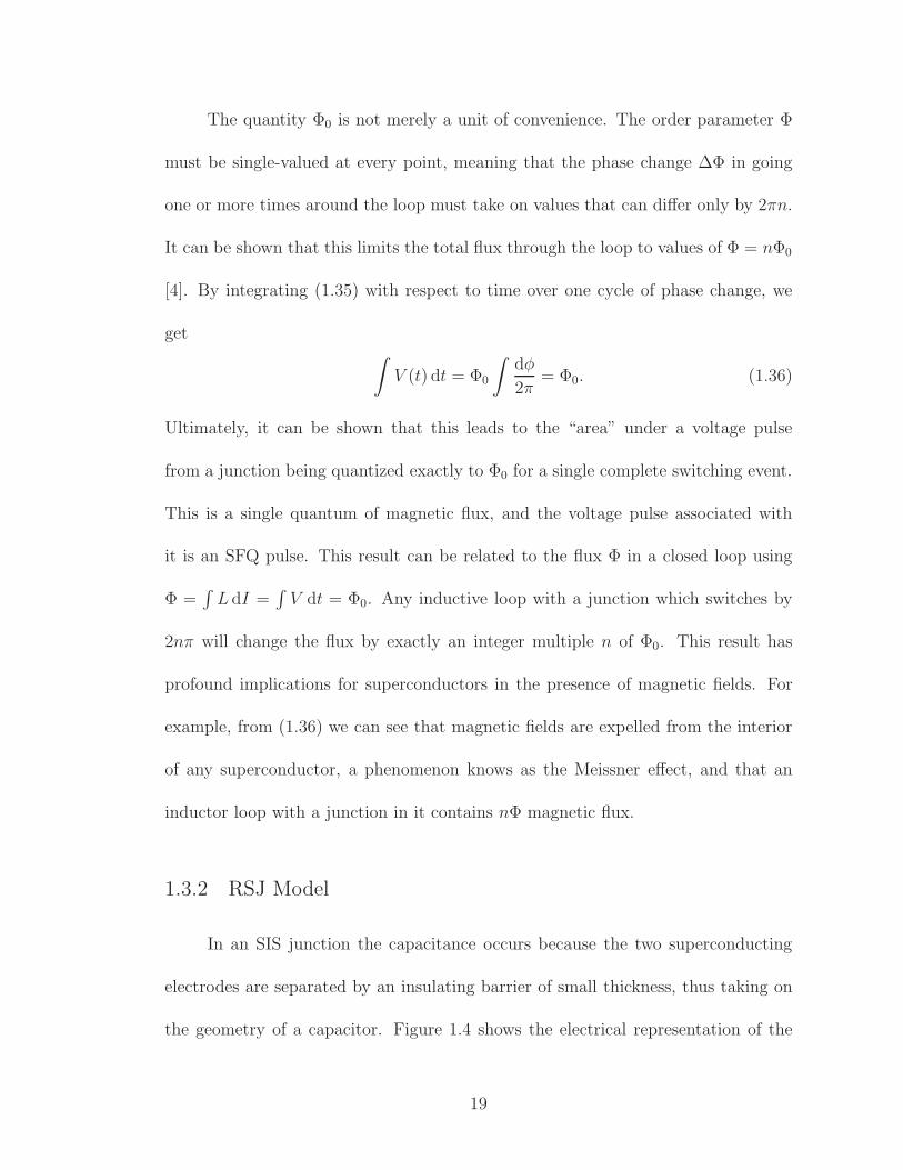
1.3.2 RSJ Model
In an SIS junction the capacitance occurs because the two superconducting
electrodes are separated by an insulating barrier of small thickness, thus taking on
the geometry of a capacitor. Figure 1.4 shows the electrical representation of the
19

RJ
(a) (b)
CIS RS Inoise
Figure 1.4: Equivalent electrical circuit of a Josephson Junction in theRSJ model. (a) Ideal Josephson junction symbol. (b) Equivalent circuitof real Josephson junctions. The Josephson junction can be treated as aparallel combination of an ideal Josephson junction with the supercur-rent IS, a capacitor C, and a non-linear resistor RJ , a shunt resistor RS
and a noise current Inoise.
Josephson junction in the resistively shunted junction (RSJ) model. A junction is
represented electrically as an ideal Josephson junction shunted by a resistor (linear or
non-linear) and a capacitance. A bias current I can be sent through the junction’s
components and can be thought of being composed of a displacement current, a
normal current, and a supercurrent. The total current through the junction can
then be written as
h C
2 e
d2φ(t)
dt2+
h
2 eRN
dφ(t)
dt+ Ic sin(φ(t)) = I + Inoise (1.37a)
This can be put in reduced form:
ω−2p φ(t) + ω−1
c φ(t) + sinφ(t) = i+ inoise =I + Inoise
Ic, (1.37b)
where ωc = (2π/Φ0)IcRN is the characteristic frequency of the junction, ωp =
1/√LcC is the plasma frequency (to be defined more rigorously in the next section),
and Lc = Φ0/(2π Ic) is the effective Josephson inductance, and RN = RJRS/(RJ +
20

RS) is the effective normal current resistance across the junction. Equation (1.37b)
rearranges the terms in (1.37a) to show the similarity to the damped harmonic oscil-
lator. The time constants of the junction are τN = RNC = ωc/ω2p and ωc = RN/Lc.
The damping factor of the junction is equivalent to the quality factor Q of the
junction, which is related to the Stewart-McCumber parameter βc by
βc = Q2 =
(ωc
ωp
)2
= ωcRNC =2e
hIcR
2NC =
2e
h(IcRN)
2 csjc, (1.38)
where the specific parallel plate capacitance is cs = C/A = ǫ0ǫr/d and the critical
current density is jc = Ic/A. For a given jc, βc is a function of cs and the IcRN
product.
It is worth pointing out that the equation of motion (1.37a) is identical to that
of a damped pendulum, in which the torque is analogous to current, the capacitance
is analogous to moment of inertia, the conductance is analogous to the damping
coefficient, the critical current is analogous to the maximum gravitational torque,
and the junction phase is analogous to angle. This analogy is useful in understanding
some of the more complex junction behavior we will shortly discuss.
Figure 1.5 shows phase diagrams in the position (ϕ) - momentum (pϕ) plane
for I = 0 of a junction for the underdamped (Q > 1), critically damped (Q = 1),
and overdamped (Q < 1) cases. The traces show the trajectories of the junction
phase. Two attractors show the equilibrium points. A sufficient increase in momen-
tum will cause the junction to switch to a different equilibrium point, generating an
SFQ pulse. The critically damped case shows a return to equilibrium in minimum
time. Underdamped junctions show oscillation before reaching equilibrium. Over-
21

damped junctions take on low values of pφ and do not oscillate but do not return to
equilibrium as quickly.
In unshunted SIS junctions IcRN = (2π/3)∆. Typically βc ≫ 1, so the junc-
tions are over damped. To decrease βc an external shunt resistor RS is added across a
junction to reduce βc, and then RN can be replaced by RN = RJRS/(RJ+RS) ≈ RS
for RS ≪ RJ , decreasing the overall shunting resistance of the junction. In most
cases RS ≪ RN and we can substitute the value of RS for RN without any further
modifications [4]. Vc = IcRN then sets the voltage scale for junction behavior, and
is typically on the order of a few mV for Nb/Al2O3/Nb junctions.
Thus the behavior of the junction is determined in design by the choice of
the shunt resistor RS, the junction area A, and the critical current density jc. For
βc > 1 the junction is underdamped and plasma oscillations with frequency ωp will
occur that will damp out on a time scale τ = RNC. For βc < 1 the junction is
overdamped and after a disturbance the phase slowly moves towards equilibrium
with a time constant 1/ωc.
The potential energy of the junction can be calculated directly from (1.34)
and (1.35). The work WS done on the junction leads directly to an expression for
the potential energy of a junction US as follows:
WS =
∫ t2
t1
IS(t)V (t) dt =Φ0Ic2e
∫ φ2
φ1
sin φ dφ
=Φ0Ic2e
(cosφ1 − cosφ2) = US(φ2)− US(φ1). (1.39)
From this we can define:
US(φ) = − cosφΦ0Ic2e
. (1.40)
22

(a) Underdamped (βc = 0.5)
φ
pφ
(b) Critically Damped (βc = 1.0)
φ
pφ
(c) Overdamped (βc = 0.5)
φ
pφ
Figure 1.5: Phase Diagram of Josephson Junction. This figure showsplots of trajectories in the phase φ and momentum pφ plane. Phase dia-grams for (a) underdamped, (b) critically damped, and (c) overdampedjunctions. In all three cases the state of the junction moves to φ = 2πn,φ = 0. Oscillations can be seen in the underdamped case.
23

This is the Jospehson energy and we can think of it as energy stored in the effective
junction inductance. For small oscillations of the phase, for which φ → φ + φ, we
can look at the variations in current Is and voltage V . Expanding (1.34) in a Taylor
series gives Is = Ic(sin φ+ cosφ× φ+ . . .). Using (1.35) to express the phase as the
integral of voltage, we get a relation between current and phase which is that of an
effective inductance:
LS IS = LSIc cosφ× φ =
∫
V dt =Φ0
2πφ, (1.41a)
and we can define the bias-dependent Josephson inductance
LS =Φ0
2πIc
1
cos φ=
h
2 e Ic
1
cosφ=
Lc
cos φ, (1.41b)
with Lc as previously defined. For bias current Ib < Ic the junction can be in the
zero-voltage (S) state where the phase is constant at φ = arcsin Ib/Ic + 2πn, where
n is an integer. The potential for a biased junction, using (1.40) in the Gibbs free
energy relation G = U − (Ib/Ic)φ [4], is
U(φ) =h
2 eIc (1− cos(φ)− i φ) . (1.42)
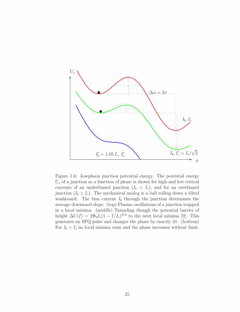
Figure 1.6 shows plots of U(φ) for the cases of a high critical current compared
to Ib, a low critical current, and an overbiased junction with Ib > Ic. Three general
situations can occur. First, for Ib < Ic a junction can exhibit plasma oscillations
about the equilibrium position. Second, if Ib is less than but close to Ic, the junction
can tunnel through the barrier to the next minimum (and possibly beyond, depend-
ing on βc) and increase its phase by 2π. Third, if Ib > Ic no minima exist and the
junction phase continuously increases with time.
24
Ib, Ic
Ib, I′c = Ic/
√2I ′b = 1.05 Ic, I
′c
∆φ = 2π
φ
Us
Figure 1.6: Josephson junction potential energy. The potential energyUs of a junction as a function of phase is shown for high and low criticalcurrents of an underbiased junction (Ib < Ic), and for an overbiasedjunction (Ib > Ic). The mechanical analog is a ball rolling down a tiltedwashboard. The bias current Ib through the junction determines theaverage downward slope. (top) Plasma oscillations of a junction trappedin a local minima. (middle) Tunneling though the potential barrier ofheight ∆U(I) = 2Φ0Ic(1 − I/Ic)
3/2 to the next local minima [9]. Thisgenerates an SFQ pulse and changes the phase by exactly 2π. (bottom)For Ib > Ic no local minima exist and the phase increases without limit.
25

1.3.3 Behavior of Overdamped Junctions
The relationship∫V dt = Φ0 for one cycle of oscillation is fundamental to all
Josephson junctions and is a key property of SFQ pulses. The case of an overdamped
junction illustrates how SFQ pulses can be generated and shows the utility of the
shunt resistor.
The equation of motion for a Josephson junction cannot in general be solved
analytically. However in the simple case of an overdamped junction where βc → 0
(which implies ωc ≪ ωp) an analytic solution can be found for a constant current.
Let ib = Ib/Ic and let time be normalized to the characteristic time 1/ωc such that
t′ = ωct. Equation (1.37b) then becomes
ib = φ(t′) + sinφ(t′), (1.43)
which has an analytic solution. We are interested in the SFQ pulse dynamics in the
I-V curve characteristics of the junction. For ib > 1 the solution to (1.43) is [4, 6]
φ(t′) = 2 arctan
(
1 + v tan(12v t′)
√v2 + 1
)
. (1.44)
where v =√
i2b − 1 is the time-averaged normalized voltage. The derivative of (1.44)
determines the voltage as a function of time.
V (t′) =Φ0
2πφ(t′) =
Φ0
2πv2
√1 + v2
sec2(12v t′)
1 + v tan2(12v t′) (1.45)
This is a periodic solution with period (in non-normalized time units)
∆t =2π
ωc v. (1.46)
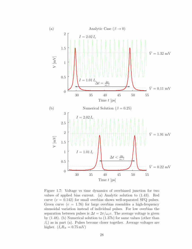
Figure 1.7 shows examples of the voltage behavior of an overdamped junction.
Figure 1.7(a) shows the solution of (1.45) for two values of Ib. Figure 1.7(b) shows
26
the numerical solutions to (1.37b) for the same values of Ib but with βc = 0.25.
Notice in Fig. 1.7 how for low values of v the junction produces individual pulses.
The average voltage V across the junction can be calculated from (1.45),
〈φ〉 = v
2π
∫
2π/v
φ(t) dt = v =√i2 − 1, (1.47)
V (Ib) =Φ0ωc
2π
√
(Ib/Ic)2 − 1. (1.48)
Figure 1.8 shows I-V curves of over- and underdamped junctions for various
values of βc. For overdamped junctions (βc < 1) the behavior is non-hysteretic. For
underdamped junctions (βc > 1), such as those we will use in RQL, the behavior is
hysteretic. Starting from zero bias current, a small increase in bias current results
in no steady voltage until the critical current is exceeded. The voltage then jumps
to a finite value instead of gradually increasing (solid black arrow). Upon decreasing
the current, the momentum of the junction can carry the phase through an infinite
number of rotations despite some dissipation so long as the bias current supplies
enough tilt to the potential. The voltage quickly decreases with decreasing current
(red arrows) and drops to zero once the curve falls below the return current Ir =
4 Ic/(π√βc) [9]. The zero-voltage branch and finite voltage branch correspond to
different initial conditions for φ(0) when solving (1.37b).
1.4 Superconducting Interferometers
In the previous section, I discussed the behavior of single junctions. Most
importantly, I have shown how flux is quantized in loops and that overdamped
27
0
0.5
1
1.5
2
30 35 40 45 50 55
V[m
V]
Time t [ps]
(a) Analytic Case (β → 0)
I = 2.02 Ic
I = 1.01 Ic
V = 1.32 mV
V = 0.11 mV
∆t = 2πωc v
0
0.5
1
1.5
2
2.5
3
30 35 40 45 50 55
V[m
V]
Time t [ps]
Numerical Solution (β = 0.25)(b)
I = 2.02 Ic
I = 1.01 Ic
V = 1.91 mV
V = 0.22 mV
∆t < 2πωc v
Figure 1.7: Voltage vs time dynamics of overbiased junction for twovalues of applied bias current. (a) Analytic solution to (1.43). Redcurve (v = 0.142) for small overbias shows well-separated SFQ pulses.Green curve (v = 1.76) for large overbias resembles a high-frequencysinusoidal variation instead of individual pulses. For low overbias theseparation between pulses is ∆t = 2π/ωcv. The average voltage is givenby (1.48). (b) Numerical solution to (1.37b) for same values (other thanβc) as in part (a). Pulses become closer together. Average voltages arehigher. (IcRN = 0.75mV)
28

0
0.5
1
1.5
2
0 0.2 0.4 0.6
I/I
c
V /IcRN
a
b
c
d
e
Figure 1.8: I-V curve of current driven junctions. Green curve shows I-Vcurve for βc = 0. For βc < 1 there is no hysteresis. For βc > 1 the red I-Vcurves shows hysteretic behavior. Curves a–e have βc = 1.1, 2, 4, 10, 30.Junctions remain in the zero voltage state (zero average voltage) untilthe critical current is reached. The voltage then jumps (horizontal blackline) to a finite value (red curves). The voltage does not return to zerountil the current has been reduced below the return current value Ir =4 Ic/(π
√β). (Results calculated numerically from (1.37b).)
29
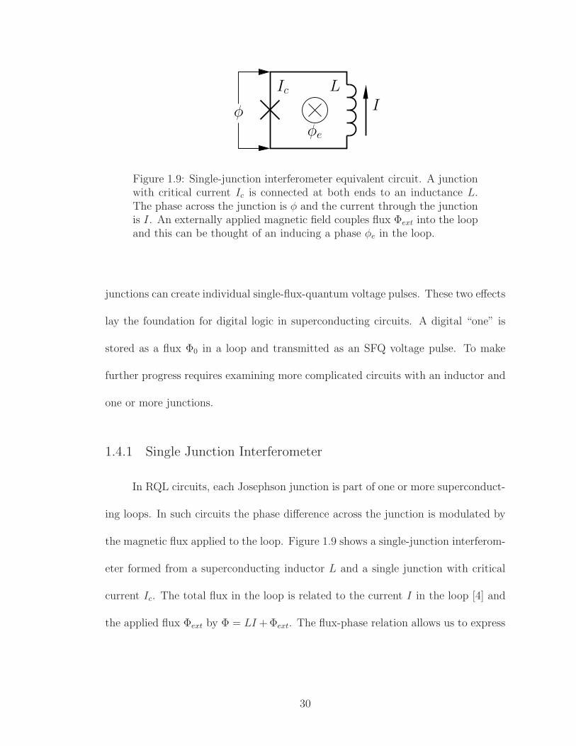
ILIc
φφe
Figure 1.9: Single-junction interferometer equivalent circuit. A junctionwith critical current Ic is connected at both ends to an inductance L.The phase across the junction is φ and the current through the junctionis I. An externally applied magnetic field couples flux Φext into the loopand this can be thought of an inducing a phase φe in the loop.
junctions can create individual single-flux-quantum voltage pulses. These two effects
lay the foundation for digital logic in superconducting circuits. A digital “one” is
stored as a flux Φ0 in a loop and transmitted as an SFQ voltage pulse. To make
further progress requires examining more complicated circuits with an inductor and
one or more junctions.
1.4.1 Single Junction Interferometer
In RQL circuits, each Josephson junction is part of one or more superconduct-
ing loops. In such circuits the phase difference across the junction is modulated by
the magnetic flux applied to the loop. Figure 1.9 shows a single-junction interferom-
eter formed from a superconducting inductor L and a single junction with critical
current Ic. The total flux in the loop is related to the current I in the loop [4] and
the applied flux Φext by Φ = LI +Φext. The flux-phase relation allows us to express
30

the phase across the junction as
φ = φe −2π
Φ0
LI = φe − λi (1.49)
where i = I/Ic, φc = 2πΦext/Φ0, and the normalized inductance of the loop is
λ = L/Lc, and Lc = Φ0/(2πIc). This gives the junction phase φ as a function of the
applied flux phase φe and the loop current I.
In a stationary state, the current through the junction obeys i = sin φ, which
allows us to rewrite (1.49) as
φ+ λ sinφ = φe. (1.50)
The phase of the single junction interferometer φ is plotted as a function of φe in
Fig. 1.10(a). For λ < 1 the junction phase follows the applied phase, φ ≈ φe.
For λ > 1 the value of φ becomes hysteretic, with only certain values of junction
phase allowed. These values correspond to the number of single flux quanta Φ0
stored in the loop. When the the junction switches, it jumps from one branch to
another. Between the branches an SFQ pulse is generated by the changing phase
across the junction and the changing current through the inductor. A different way
to understand these jumps is to look at the energy of the loop, including both the
junction and the inductor. This gives an energy in terms of the phases φ and φe as:
U(φ) = IcΦ0
(
1− cosφ+(φ− φe)
2
2λ
)
. (1.51)
This is plotted in Fig. 1.10(b) for the special case of φe = π/2, which makes the
energy symmetric about φ = 0. In switching between the two lowest minima, no
energy is dissipated and the switching behavior back and forth is the same.
31

-2
-1
0
1
2
3
4
-10 -5 0 5 10 15
JunctionPhaseφ/π
Applied External Phase φe/π = 2Φe
Φ0
Junction phase branches(a)
0
0.2
0.4
0.6
0.8
1
1.2
-3 -2 -1 0 1 2 3
Energy
[E/Φ
0I C
]
Phase ϕ [rad/π]
(b) Single-junction Interferometer Potential Energy
Figure 1.10: Single-junction interferometer phase behavior and potentialenergy. (a) The junction phase φ is plotted as a function of the externallyapplied phase φe showing both the allowed branches (red solid) andprohibited branches (green dashed). A transition from one branch tothe next results in an integer change of the number of flux quanta Φ0 inthe interferometer. (b) Potential energy (red solid curve) of the single-junction interferometer when biased by Φ0/2 flux in the loop. Solidand empty circles show two meta-stable states at equal energies. Greendashed curve shows quadratic term in (1.49).
32

This behavior will become very important in the next chapter, in which I
describe the nature of a new logic family. We wish for a symmetry between positive
flux and negative flux. With this kind of symmetry in a single loop interferometer,
no power will be dissipated by switching events.
1.4.2 Josephson Transmission Line
In this section I briefly discuss the Josephson transmission line (JTL). A
Josephson transmission line is a series of single junction superconducting interfer-
ometers coupled together by inductances L. It is of fundamental importance to RQL
because it can carry SFQ pulses from one junction to another. The basic concept
of the JTL can be seen in Fig. 1.11. A constant bias current — less than Ic and by
convention about 0.7Ic — is supplied to each junction. The current of an SFQ pulse
causes the underbiased junction to become overbiased and switch through a phase
of 2π. This switching generates new SFQ pulses which travels both backwards,
canceling out the original SFQ pulse, and forwards, allowing a pulse to propagate
forward.
When multiple junctions and inductors L are coupled together, (1.37b) can be
generalized and one finds:
Φ0
2πL(−φi−1(t) + 2φi(t)− φi+1(t)) =
− ω−2p φi(t)− ω−1
c φi(t)− sin (φi(t)) + Ib, (1.52)
where i refers to the ith junction in the JTL and Ib is a generic externally applied
bias current. The left hand side of the equation describes the currents flowing
33

to and from the ith single-junction interferometer loop. On the right-hand-side of
the equation we see the regular terms from (1.37b) and a biasing function of our
choosing. On the left-hand-side are the coupling terms between junctions, which are
simply the currents flowing through the inductors from the previous (i−1) and next
(i + 1) junctions. The set of equations for i = 1, . . . , N , plus boundary conditions,
forms the equations of motion for the whole transmission line. (This is in fact a
discreetized version of the sine-Gordon equation, which implicitly has solutions of
traveling SFQ pulses [6].)
The JTL configuration shown in Fig. 1.11 will allow positive pulses to travel
rightward and negative pulses to travel leftward. Negative pulses will travel right-
ward if the direction of the bias current is reversed. We have a choice of Ib. If
the bias current is supplied through coupled inductors, the junction forms a single
junction interferometer, and the switching can occur between equipotential states.
If the bias current is not constant but can vary over time and (discreetly) over space,
we can control the flow of pulses. In RQL, one chooses Ib = A sin(ω t) so that both
positive and negative pulses travel rightward during opposite clock phases.
The solution to (1.52) for Ib = A sin(ωt) is shown in Fig. 1.12 for four junc-
tions, each on two phases. (See Appendix A.) The propagation of pulses is clear.
I also note another important fact, that pulses can be held at a “phase boundary”
between different bias conditions. Also it is clear that the junctions can propagate
both positive and negative pulses. The detailed behavior of such an arrangement of
Josephson junctions is the topic of the rest of this thesis.
34
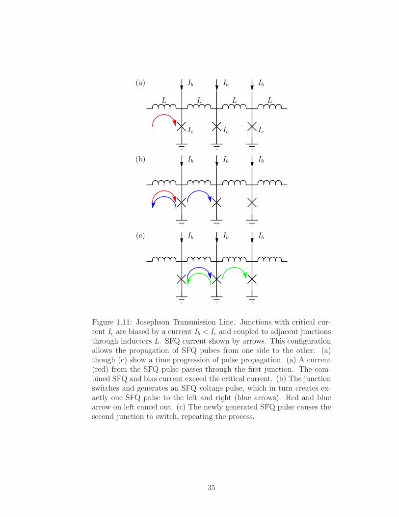
(a)
Ib Ib Ib
IbIb Ib
Ib Ib Ib
IcIcIc
L L L L
(c)
(b)
Figure 1.11: Josephson Transmission Line. Junctions with critical cur-rent Ic are biased by a current Ib < Ic and coupled to adjacent junctionsthrough inductors L. SFQ current shown by arrows. This configurationallows the propagation of SFQ pulses from one side to the other. (a)though (c) show a time progression of pulse propagation. (a) A current(red) from the SFQ pulse passes through the first junction. The com-bined SFQ and bias current exceed the critical current. (b) The junctionswitches and generates an SFQ voltage pulse, which in turn creates ex-actly one SFQ pulse to the left and right (blue arrows). Red and bluearrow on left cancel out. (c) The newly generated SFQ pulse causes thesecond junction to switch, repeating the process.
35

Ib = 0.7 sin(ωt) Ib = 0.7 sin(ωt+ π/2)
SFQ Input LLLLLLL
JJ1
RN
JJ2 JJ3 JJ4 JJ5 JJ6 JJ7 JJ8
-1
-0.5
0
0.5
1
1.5
2
100 120 140 160 180 200 220 240-1-0.500.51
JunctionPhase[rad/2π]
Clock
Amplitude[I/I
c]
Time [ps]
JJ 1JJ 2JJ 3JJ 4JJ 5JJ 6JJ 7JJ 8
Phase 1 ClockPhase 2 Clock
Figure 1.12: Phase behavior of junction in JTL. The solution to (1.52)for the circuit schematic shown on top is shown with phases φ1 to φ8
driven by the bias current shown on bottom. Junctions 1 – 4 are drivenby black sinusoid, junctions 5 – 8 by the red sinusoid, a quarter periodlater. The junctions can be seen to switch in sequence with the later fourjunctions switching only when the local bias current is high. (Junction8 is highly damped to prevent reflections and does not actually switchitself.) The first junction is driven by a positive SFQ pulse followed bya negative SFQ pulse half a period later. (Numerical solution. IcRN =0.75, βc = 1.56. Further details found in Appendix A.)
36

1.5 Introduction to Superconducting Digital Logic
Moore’s Law predicts that the speed of digital electronics will increase by a
factor of two every two years. This has been achieved in practice by making CMOS
circuits smaller and smaller. Recently, this progress has slowed and CMOS has
been stuck at clock speeds of around 4 GHz for the last few years [14]. Faster
circuits have come at the cost of higher power dissipation and heat loading. This is
one factor limiting progress of CMOS technologies. Multi-processor schemes have
allowed further throughput improvements, however this is expected to reach a limit,
too. Parallel processing introduces an overhead which some have predicted will
impact performance at about 16 processing units [14]. To break through these
limitations, a new class of digital circuits is needed.
Some type of superconducting digital electronics may ultimately fill this need.
Superconducting technologies have a number of inherent advantages over CMOS.
The flux in a superconducting ring is quantized to exactly h/2e making digital
one and digital zero intrinsically defined quantities in the system. In Josephson
junctions, creating one such quantized flux corresponds to an energy consumption
of typically about 10−18J , far lower than that for CMOS [14]. Also, the inherent
switching speed of junctions is fast; 1 mV applied potential corresponds to a 500
GHz oscillation frequency. Of course, CMOS technology also has many advantages,
and developing a new technology that can compete with CMOS is not easy.
The first logic based on the processing of SFQ pulses was Rapid Single Flux
Quantum (RSFQ) logic [15]. In RSFQ circuits, digital one and digital zero are en-
37

coded as the presence or absence of an SFQ pulse between two clock pulses. Within
one clock period, the data is stored as magnetic flux states of superconducting in-
terferometers. Clock pulses are used to read the state of internal memory and reset
gates. RSFQ logic has demonstrated fast operating speeds [16] (up to 700 Gbit/s in
a static divider), low dynamic power dissipation [17] (a few mW for a whole circuit)
[6], chip-to-chip communication of more than 100 Gbit/s [18, 19], and an integration
density of tens of thousands of junctions per chip [20], on demonstrated prototypes
[21, 22].
However, RSFQ has some issues. For example, pulse encoding used in RSFQ
logic imposes some limitations. RSFQ uses a ripple clock distribution where active
elements — the Josephson junctions — regenerate the clock pulses. The ripple-
clock distribution necessitates active hardware delays between gates and leads to a
jitter accumulation [23]. The internal memory of the gates inherently leads to large
latency, as the resetting clock signal must propagate through the whole circuit.
Another problem is that the DC power scheme uses bias resistors that give at least
ten times higher static power dissipation than the switching power [24]. Also, RSFQ
circuits are built from finite-state machines and pipelined on the gate level. This
allows high throughput at the cost of high latency. Together these properties limit
application of RSFQ and make it unsuitable for VLSI applications such as high end
computing where operations-per-Joule and latency are prime performance metrics
[25].
Many challenges have prevented of superconducting technologies from seeing
widespread use in the past. However, recently a number of superconducting digital
38

electronics have found commercial use. Advances in cooling technology make space-
and energy-efficient options available for computing [14]. Digital signal processors,
adaptive filtering, and direct digitalization has all been performed in a commercial
setting using superconducting digital electronics. Despite these advances, a number
of issues still remain. In particular, the lack of existing superconducting digital
memory prevents its use as a general purpose computer that can compete with
silicon-based processors.
39


Chapter 2
Reciprocal Quantum Logic
2.1 Introduction
Power consumption has increasingly become a limiting factor in high perfor-
mance digital circuits and systems. According to a U.S. Environmental Protection
Agency study [26], the demand of servers and data centers in the U.S. is approach-
ing 12 GW, equivalent to the output of 25 typical 500 MW power plants. Here
I describe a new logic family, Reciprocal Quantum Logic, that yields a factor of
300 reduction in power compared to projected nano-scale CMOS, even taking into
account the power consumed to maintain a cryogenic operating temperature. In
this chapter I discuss the fundamentals of reciprocal quantum logic. I first describe
an RQL transmission line and RQL logic gates. I then describe three benchmark
experiments that I completed that show the scalability of RQL for very large scale
integrated (VLSI) circuits.
In this introduction I describe the encoding of classical digital data using
reciprocal SFQ pulses. RQL gates, operate with single magnetic flux quanta (SFQ)
generated by overdamped Josephson junctions. This is the same approach used in
RSFQ gates. Figure 2.1 illustrates how data is encoded in RQL. A “one” bit is
encoded as a pair of positive and negative (reciprocal) SFQ pulses generated in the
positive and negative phases of the sinusoidal clock. A “zero” bit corresponds to
41

the absence of positive/negative pulse pairs during a clock cycle. The positive SFQ
pulse arrives during the positive part of the clock signal while the negative pulse
follows later during the negative part of the clock cycle.
A major difference between RQL and RSFQ is how power is supplied to the
gates. RSFQ gates [4] use static dc power applied in parallel through bias resistors,
while RQL uses ac power applied in series. Figure 2.1 shows the AC power applied
through the inductively coupled bias line; the AC power simultaneously serves as a
global clock reference. With no bias resistors there is no static power dissipation.
Power induced in LAC is conservative apart from junction switching events.
2.2 Josephson Transmission Line
Figure 2.2 shows the schematic of an RQL Josephson transmission line. The
JTL is formed from a series of cells with each cell being an inductive loop formed
by junctions JJ1 and JJ2 and inductors L1 and L2. The inductances L1 and L2
are small (L1Ic1 ≪ Φ0) so an incoming SFQ pulse will induce switching of both
junctions in series. Junctions are biased through inductor L0 which is coupled to
the AC line inductance Lc via a mutual inductance M0c. AC current in the clock
line induces positive bias current through the junctions in the positive half-period
of the clock cycle and negative current during the negative half-period. The flux
bias inductor Lb is large (LbI1 > Φ0) and any junction connected directly to a bias
inductor (L0) forms a single junction interferometer with two stable states, similar
to the single junction interferometer circuit shown in Fig. 2.1. The circuit in Fig.
42

SFQ
1 10 0
time
Voltage
Current
Data
acpow
er
clock
signal
J1
Lclock
LACk
LS
RN
SFQ Pulse
Clock AC Power
Figure 2.1: Basic RQL active interconnect element showing groundedjunction J1 coupled inductively to clock line. Junctions are coupled toother elements through LS. The interconnect draws energy from thepower line, much like an RSFQ JTL. This element provides isolation,amplification of the current with a characteristic delay. The junctionand bias inductor LAC form a single-junction interferometer.
43

(c)clock line
flux bias
L2L1
JJ1 JJ2
Lb
Lc
L′
1 L′
2
00
L0
Lc
JJ1
data line
L1
L0
(a) (b)
(d)
Figure 2.2: Josephson transmission line and SFQ launch circuit diagram.(a) Circuit diagram for RQL JTL. The values of inductors are: L0 =13.4 pH, L1 = L′
1 = 3.0 pH, L2 = L′2 = 2.1 pH, M0b = 0.5 pH, M0c =
1.7 pH. The critical currents for the junctions are: JJ1 = 0.100mA,JJ2 = 0.141mA. (b) Circuit diagram for RQL launch. (c) Block diagramsymbol of JTL, with two digits indicating phase and clock line number.(d) Block diagram symbol of launch.
2.2 is electrically equivalent to that shown in Fig. 2.1 for LAC = L1 + L0/2 and
LS = L′1 for JJ1 and LAC = L2 +L0/2 and LS = L′
2 for JJ2. A single flux quantum
Φ0 will be stored in the loop formed by the junction J1 and bias inductor after each
increase of the phase by of the junction by 2π. This stored flux is canceled out by the
reciprocal pulse. Additional DC flux bias on the clock line induces a flux of Φ0/2
in the bias inductor. This makes the states of the single-junction interferometer
symmetric with ±Φ0.
The RQL JTL is known to have wide operating margins, more than 50%
on individual critical currents [27]. The critical parameter found in our simulations
turns out to be the ratio between bias inductor Lb and transmission inductor L1+L2.
The bias inductor Lb needs to be as large as possible so the current in the bias
44
inductor does not effect junction switching. However, for practical reasons bias
inductors need to be limited in size. Values in Fig. 2.2 correspond to the nominal
design I used.
RQL JTLs allow amplification of SFQ pulse energy. This is achieved by step-
ping up the critical current from one cell to the next. With two sequential steps with
amplification by√2, the energy of the SFQ pulse is doubled. The nominal design
values I used corresponds to an amplification of the SFQ energy by√2 per stage.
This allows me to use the same JTL cell layout as part of an RQL SFQ splitter. An
RQL splitter is formed by attaching the input of two JTL units to the output of a
single JTL. This effectively gives the JTL unit a fan-in of one-half and a fan-out of
one.
Many cells can be connected in series to form a long JTL. A pulse will prop-
agate through a JTL segment so long as the bias current is sufficient. However,
one-phase AC power does not provide directionality for pulses. Using only one
phase, during the negative half-cycle, junctions will switch in the opposite order
and a positive pulse — which moved forward during the positive half clock cycle —
would travel backward during the negative half. To prevent this, RQL uses a four-
phase clock; two clock lines with a phase difference of π/2 provide two phases. By
coupling the clock lines to the junctions in a wound or counter-wound fashion one
produces a total of four phases differing by 0, π/2, π, and 3π/2. With four phases,
when one phase is nearing the end of the “timing window,” the next has already
started, allowing a pulse to continue onward. (I will give a precise definition of the
timing window in Chapter 3. For now, it can be thought of as the time during which
45

the clock is close to maximum amplitude, approximately the third of the period in
which the AC signal has half its maximum amplitude or higher current.) For slower
clock speeds, the pulses will wait for the rise of the next clock phase.
Figure 2.3 shows a four-phase RQL JTL. Given the geometry of two clock
lines and two winding directions, the natural way to index the clock phases is with
a two-bit binary in which the first digit is the winding bit and the second the clock
line bit. The first clock line (0 phase) with regular winding is 00 and the third (π
phase), for example, is 10.
The four-phase clock provides an implicit pipeline — data processing elements
with the output of one element as the input of the next one — without additional
devices needed for latches or clock distribution. However, in cases where the phase
of the clock on the next element is delayed by π/2 relative to the current JTL, JTLs
on such phase boundaries require slightly altered values compared to the inductors
shown in Fig. 2.2. Because of the phase difference, the bias current through adjacent
junctions will cause current to leak from one JTL to the next. This can be prevented
by altering the inductance values so as to redistribute the currents correctly. A
pipeline in RQL can have any number of logical elements on a single phase, i.e. the
elements are connected in series to a single clock line with a single phase. Short
pipelines can have higher operating frequencies with fewer operations per phase.
Long pipelines, such as shown in seen in Fig. 2.4, can have more logical operations
per phase at the cost of lower operating frequency; the SFQ pulses must reach the
next phase before the current becomes too small to bias the junctions. In general,
the speed of large circuits is effectively the product of clock frequency and pipeline
46

(c)
(b)
(a)
#1 #2 #3 #4
Clock 1Clock 2
Direction of Travel
#4#3#2#100 01 10 11
+Φ0−Φ0
Negative SFQ Positive SFQ
Phase 00 Phase 01 Phase 10 Phase 11
Clock 1
Clock 2
Figure 2.3: Data propagation in an RQL 4-phase clock transmissionline. (a) Two clock signals with a quarter-period offset between them.(b) Aligned with the waves in (a), this figure shows four JTL units inseries on four different phases labeled 00, 01, 10, and 11. Two clock linesprovide four phases by counter-winding, shown by inductors pointingin opposite directions. Pulse directionality is achieved by a four-phaseclock. A positive flux propagates bias current is positive, and a negativepropagates forward when the bias current is negative. Positive and nega-tive SFQ pulses represented by the current generated by their flux in twopairs of junctions each. Positive pulses drives bias current down bothjunctions, and the rightmost will switch first. Negative pulses drive biascurrent upward though junctions; again the right junction of the pairswitches first. (Only coupled inductors are shown for clarity.) (c) Blockdiagram of the circuit shown in (b).
47

00
00 00 00 00
+Φ0
#1 #2 #3 #4
#4#3#2#1
00 00 00
Figure 2.4: Deep Pipeline JTL. Four JTL units are on the same clockphase with a single positive SFQ pulse traveling left-to-right. The recip-rocal pulse comes later. Pulses travel through any number of junctionsprovided that the bias current is correct. Pulses propagate through junc-tions until a clock phase boundary is reached. This decreases latency asthe pulse can travel though more junctions per clock cycle.
depth.
RQL pipelines are robust against timing errors. The data self-synchronizes to
the AC clock signal. At a phase boundary — where junctions are coupled to a clock
line with different phase — early pulses wait for the rise of the clock signal in the
next section. The jitter accumulates only within one pipeline stage and is negligible.
Nominally timed pulses have a window during which propagation is possible. Unlike
in RSFQ, pulses do not need to wait for a specific clock SFQ pulse to propagate.
The hold-and-release operation in RSFQ fixes the clock speed to a specific value. In
RQL, the clock speed can be changed freely up to a maximum (which will be derived
in Chapter 3). Timing errors can generally be corrected by reducing the clock speed;
every pipe can be operated at a lower frequency and the pulses will wait at the pipe
48
phase boundary. The maximum pipeline depth in terms of Jospheson junctions is
determined by the operating clock frequency fclock and the delay time per cell. The
delay of a pipeline should be less than approximately one-third of a clock cycle. I
give a detailed description of RQL timing in Chapter 3.
2.3 Logic Gates
The routing and processing of pulse-based signals is distinct from transistor-
based voltage-state logic. In RQL, logic is performed by routing pulses though an
inductive network. The Josephson junctions in the JTLs act as signal repeaters.
Considering only the positive pulses, the gates are similar to the state machines
of RSFQ logic. The trailing negative pulse erases the internal state every clock
cycle. Logic gates are unclocked. The timing and bias depend on input and output
JTLs connected to the gate. There are three fundamental RQL gates that form a
complete set [28] and thus can be used to build any digital circuit: the AndOr gate,
the AnotB gate, and the Set-Reset latch.
2.3.1 AND and OR Gates
Figure 2.5(a) shows a schematic of the AndOr gate. The gate has two sym-
metric inputs and two outputs. The first pulse the gate receives on either input is
routed to the OR output; the second to the AND output. The gate contains two
junctions that are connected to the inputs through inductive networks formed by
two high-efficiency transformers, k12 and k34. The high-efficiency transformers form
49

AB
L4
L1
L2
L3
k23
k34
Bias In
B
A
JJ2
JJ1
Bias Out
L5 L6
AANB
B
A
L1
k34
JJ2
JJ1
Bias OutBias In
L2 L3 L4
k12
L5
L6
OR
AND
(b) (c) (d)
(a)
(f)
(e)
Figure 2.5: RQL Logic Gates. (a) AND and OR logic gate schematic.Inputs A and B are highly coupled through k12. The high common modeinductance drives currents through both junctions upon SFQ input. Fluxbiasing through k34 biases JJ1 to switch first, after which the flux biasesJJ2. Low odd-mode inductance between L1 and L2 prevents switchingjunctions from generating backwards-traveling SFQ pulses. (Optionalcircuit elements shown in grey.) The values of inductors are: L1 =L2 = 26.9 pH, L3 = L4 = 9.8 pH, L5 = L6 = 3.0 pH, M12 = 24.8 pH,M34 = 0.57 pH. The critical currents for the junctions are: JJ1 = JJ2 =0.141mA (b–d) Symbols for OR, AND, and the combined AndOr gate.(e) Schematic for the A-and-not-B (AnotB) logic gate. A pulse at Bbefore A will reverse-bias JJ2 though the high efficiency k34 transformer,inhibiting output. A pulse at A before B will pass though uninhibited.The values of inductors are: L1 = L2 = 3.25 pH, L3 = 28.3 pH, L4 =32.3 pH, L5 = 4.2 pH M23 = 0.525 pH, M34 = 15.76 pH. The criticalcurrents for the junctions are: JJ1 = JJ2 = 0.100mA (f) Symbol forAnotB gate.
50

a high-inductance differential mode between inputs and a low-inductance common
mode between the inputs and the junctions. A pulse at either input will send cur-
rent through both junctions. The junction JJ1 at the OR-output is preferentially
biased by Φ0/2 flux induced in inductor L4. This junction will switch when the first
input pulse on either input arrives. After switching, the flux state of the gate is
reversed and junction JJ2 at the AND output becomes preferentially biased. This
means that junction JJ2 will switch if a second positive input pulse arrives. The
high differential inductance between inputs prevents propagation of the input pulses
from one input to the other. Negative pulses are processed in a similar way, except
that junction JJ2 at the AND output will switch first in the case of two input pulses.
The first negative pulse will follow the second positive pulse in this case, and the
second negative pulse will follow the first positive pulse. This switching does not
violate the RQL data encoding, which requires that every positive pulse is followed
by a negative pulse approximately half a clock period later, since all positive pulses
on the output are followed by reciprocal pulses. The ordering for negative pulses is
reversed, though this is only a timing issue and not a logic error.
I note that the AndOr gate does not have an explicit clock bias. The bias
current for the junctions is provided from input JTLs. The input JTLs to the gate
require special parameters and negligible output inductance. The combination of
L1, L2, and k12 produce a total inductance of 5.1 pH, the same as the JTL would
see when connected to another JTL. The AndOr gate parameters are optimized in
such a way that the signal is amplified at the input of the gate and there is sufficient
bias current to switch the junctions in the gate. The critical margin in the AndOr
51

gate is on the dc bias inductor. The margins on other parameters are more than
50%. The gate has a fan-out of one-half and requires one standard JTL segment at
the output to connect to other gates.
The AndOr gate does not have timing restrictions on input signals. If both in-
puts arrive simultaneously, both junctions switch and produce simultaneous output
at the AND and OR outputs. The internal flux state of the gate does not change in
this case. The gate can operate either at a phase boundary or inside a single-phase
pipeline. Similar to standard JTLs, the input and output JTLs for the AndOr gate
have adjusted parameters that compensate for differences in bias current at the
phase boundary. The AndOr gate can be used as a stand-alone OR or AND gate.
Either (but not both) of the inductors L5 and L6 are optional in cases where only
one of the two logic functions is desired.
2.3.2 A-and-not-B Gate
Figure 2.5(e) shows a schematic of the AnotB gate. The A-and-not-B (AnotB)
gate allows pulses arriving at A to pass through as long as a pulse has not arrived
previously at B. The gate consists of two junctions, JJ1 and JJ2, connected through
a high-efficiency transformer k34. The high efficiency transformer “negatively” cou-
ples the junctions to each other; a positive current through one junction induces a
negative current through the other, and vice versa. Therefore, when an input pulse
arrives at the B input and JJ1 switches, a negative current is induced through JJ2,
which inhibits it from switching. In this case an A-input pulse is stored in input
52

inductor L5 and will annihilate with the reciprocal pulse half a cycle later. In the
absence of a B-pulse, junction JJ2 switches with each incoming A-input pulse.
The AnotB gate has a bistable internal flux state corresponding to ±Φ0/2.
The gate has a DC flux bias line that sets up a positive current through both
junctions to ground. When either junction is triggered by an SFQ pulse, the flux
state is reversed, which reverses the current through the junctions and inhibits the
triggering of the other junction.
The biasing and input/output JTL parameters are the same as for the AndOr
gate. However, the AnotB gate has specific timing requirements. The pulse on the
B-input has to arrive before or simultaneously with the A-input pulse. The later
case can be realized by placing the AnotB gate at a phase boundary. For this reason
this gate is often placed at a phase boundary to save on explicit hardware delays.
2.3.3 Set-Reset Gate
The Set-Reset gate shown in Fig. 2.6(a) is the most complicated RQL gate I
have worked with. The gate is complicated because the attraction of positive and
negative reciprocal pulses makes it difficult to realize internal memory. The Set-
Reset gate has an internal state which switches between two bi-stable flux states. A
positive pulse is output when the internal state switches to the positive flux state.
A negative pulse is output when the state switches to the negative flux state. The
state changes only for the first SFQ pulse pair on either input; later pulses do not
switch the state or generate output. The waveforms during gate operation are shown
53
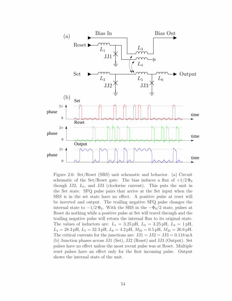
Set
Reset
Output
timephase
0
timephase
0
timephase
0
JJ3JJ2
JJ1
Bias In Bias Out
Output
L3
L5
L4
L6L2
L1
Set
Reset
(a)
(b)
2π
2π
2π
Figure 2.6: Set/Reset (SRS) unit schematic and behavior. (a) Circuitschematic of the Set/Reset gate. The bias induces a flux of +1/2Φ0
though JJ2, L5, and JJ3 (clockwise current). This puts the unit inthe Set state. SFQ pulse pairs that arrive at the Set input when theSRS is in the set state have no effect. A positive pulse at reset willbe inverted and output. The trailing negative SFQ pulse changes theinternal state to −1/2Φ0. With the SRS in the −Φ0/2 state, pulses atReset do nothing while a positive pulse at Set will travel through and thetrailing negative pulse will return the internal flux to its original state.The values of inductors are: L1 = 3.25 pH, L2 = 3.25 pH, L3 = 1pH,L4 = 28.3 pH, L5 = 32.3 pH, L6 = 4.2 pH, M35 = 0.5 pH, M45 = 26.6 pH.The critical currents for the junctions are: JJ1 = JJ2 = JJ3 = 0.118mA(b) Junction phases across JJ1 (Set), JJ2 (Reset) and JJ3 (Output). Setpulses have no effect unless the most recent pulse was at Reset. Multiplereset pulses have an effect only for the first incoming pulse. Outputshows the internal state of the unit.
54
in Fig. 2.6(b).
The Set-Reset gate consists of three junctions. Junctions JJ2, JJ3, and the
inductor L5 form the Set memory loop. Junction JJ1 and inductor L4 form the
Reset memory loop. Both loops are coupled to each other through the high-efficiency
transformer k35. The Set memory loop is initially biased to have +1/2Φ0, so JJ3 is
preferentially biased with positive current and JJ2 has a negative current. Junction
JJ2 has a small critical current so that it will switch despite the positive flux in the
loop. This leaves the internal flux in the Set loop at +3/2Φ0. JJ3 then switches,
producing a positive output, and returns the internal flux to +1/2Φ0. The reciprocal
pulse switches JJ2 and changes the internal flux from +1/2Φ0 to −1/2Φ0. Any
further set pulses will simply change the internal state from −1/2Φ0 to +1/2Φ0
(the leading pulse) and back (the reciprocal pulse) without causing any output.
The above process continues until a Reset pulse switches junction JJ1. In this
case, −Φ0 is applied to the Set loop and the flux state in the set loop becomes
−3/2Φ0. A negative output follows when JJ3 switches and returns the internal flux
state to −1/2Φ0. The following reciprocal Reset pulse switches the internal state
to +1/2Φ0. Following Reset pulses will switch the internal state back and forth
between −1/2Φ0 and +1/2Φ0, similar to the above behavior of the Set pulses.
For the gate to work properly, the Set and Reset pulses must arrive with a half-
phase delay between them. To see why, notice that a positive Reset pulse generates
a negative output pulse. In order for this pulse to propagate, it must wait for or
be generated during the negative clock cycle on the output. For this reason, the
Set-Reset gate must operate on a mixed phase boundary with the Set input on the
55
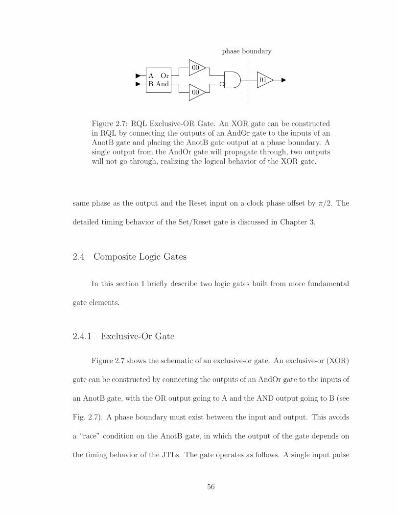
And
00
00
01
phase boundary
AB
Or
Figure 2.7: RQL Exclusive-OR Gate. An XOR gate can be constructedin RQL by connecting the outputs of an AndOr gate to the inputs of anAnotB gate and placing the AnotB gate output at a phase boundary. Asingle output from the AndOr gate will propagate through, two outputswill not go through, realizing the logical behavior of the XOR gate.
same phase as the output and the Reset input on a clock phase offset by π/2. The
detailed timing behavior of the Set/Reset gate is discussed in Chapter 3.
2.4 Composite Logic Gates
In this section I briefly describe two logic gates built from more fundamental
gate elements.
2.4.1 Exclusive-Or Gate
Figure 2.7 shows the schematic of an exclusive-or gate. An exclusive-or (XOR)
gate can be constructed by connecting the outputs of an AndOr gate to the inputs of
an AnotB gate, with the OR output going to A and the AND output going to B (see
Fig. 2.7). A phase boundary must exist between the input and output. This avoids
a “race” condition on the AnotB gate, in which the output of the gate depends on
the timing behavior of the JTLs. The gate operates as follows. A single input pulse
56

will produce a single output on the OR-output. The output pulse then travels to
the AnotB gate where it must wait until the clock rises on the output JTL (marked
01 in the figure). Provided a second pulse never came, the output of the AnotB
gate will not be inhibited. If a second pulse comes, regardless of timing (but on
the same clock phase) both pulses will arrive at the AnotB gate and no output will
occur. The XOR gate is particularly important for my work because the carry-look
ahead adder (Chapter 6) is composed of both AnotB and AndOr gates as in the
XOR gate.
2.4.2 Non-Destructive Read-out Gate
The Set-Reset gate is inherently destructive in the sense that any output re-
sults in a of the change of the internal flux state. To preserve an internal flux state
after multiple read operations we can use a Non-Destructive Read-out (NDRO)
Gate. Figure 2.8 shows the schematic of the NDRO gate. In this gate, the Set-
Reset gate allows either a positive pulse or a negative pulse to be propagated to
the B-input of an AnotB gate. Because the reciprocal pulse only follows when the
next Reset (or Set) pulse arrives at the Set/Reset gate, the AnotB gate will remain
in the output-inhibiting flux state. Pulses from the read input will not generate
output, nor will the internal flux state change after many read inputs.
57

(b)
OutputReset
Set
OutputReset
Set
Reset
Set01
0000
10
Reset
Set
Read 00
01
0000
10
(a)
Figure 2.8: Non-Destructive Read-Out Gate. The NDRO gate servesas a memory unit. The Set-Reset gate only outputs a pulse when theinternal state changes. By including an AnotB gate the internal statecan be determined repeatedly without changing the state. (a) In thisconfiguration a read RQL pulse will be output from the AnotB gate uponinput at the Read input, depending on the internal state of the Set-Resetgate. (b) In this configuration a constant series of self-generated SFQpulse pairs continuously read the state of the Set-Reset gate. This willgenerate output SFQ pulses every clock cycle until the Set-Reset gategets a reset signal.
58

2.5 Fabrication and Equipment
2.5.1 Fabrication
I had test gate circuits fabricated at Hypres using their 4.5 kA/cm2 process.
(Further details of the Nb/AlOx/Nb fabrication process can be found in Appendix
E.) These chips were given the name Monrovia20. This chip contained experiments
for logic and power tests.
Circuits fabricated in Hypres’ superconductor fabrication process with 4.5 kA/cm2
Josephson junction critical current density have a 1.5µm minimum feature size [29].
(See Appendix E.) The process contains four Nb metallization layers. The sec-
ond and third layers are used for wiring, Josephson junctions, and gate inductances
while the first and fourth metallization layers are used as superconducting ground
planes. I designed AC clock lines as microstrips with signal in the first metal layer
and ground in the fourth metal layer, connected to the first layer ground through
frequently spaced vias. This topology of clock lines gives a high yield because it
avoids step coverage problems and film defects in higher metal layers. It also pro-
vides a superconducting shield above the signal wire that reduces cross-coupling
between adjacent lines. The impedance of the line is limited to 42Ω because the
width is limited to the minimum feature size of the signal layer (2.3µm) and the
SiO2 isolation has a thickness of 850 nm. (A 50Ω line would be realized with a
2.0µm wide microstrip in the first layer with a ground plane in the fourth layer.)
The shift register was fabricated in four metal layers by Hypres with 4.5 kA/cm2
critical current density and 1.5µm minimum feature size. The junction plasma
59

Figure not to scale.
Dielectric
M3
M2
Via
M0 (Ground)
M0 (Signal)
Substrate
(top)
(front) (side)
Figure 2.9: RQL Clock Line Transformer Layout. The transformer cou-pling junctions to clock lines are shown here in three orthogonal views.On the bottom of the chip moats separate the M0 signal line (light red)from the M0 ground plane (red). The M3 layer (dark blue) is con-nected to the M0 ground plane with vias, creating a grounded skyplane.This creates a microstrip. The transformer is fabricated by depositinga second microstrip in M2 (green) between the M0 signal line and theskyplane. The transformer is grounded on one end by a via connectingto the skyplane. The mutual inductance between M0 and M2 inducescurrents through the junction (not shown in figure). The M2 transformerextends over the edges of the M0 signal line to ensure that misalignmentduring fabrication does not affect the mutual inductance between M0and M2. Cut-away views.
frequency was ωp/2π = 250GHz. This gives a minimum SFQ pulse width of
τp = 1/ωp = 3ps. The clock lines are 2.3µm wide strips (the minimum width)
with 850µm SiO2 dielectric thickness to the ground plane1. This gives a maximum
impedance of 32Ω. Tapered lines between pads and circuit provided impedance
matching. (See Chapter 4 for details on the power delivery network.)
Figure 2.9 shows the design of the transformers that couple the junctions to
1The ground plane is the top metal layer in this design
60
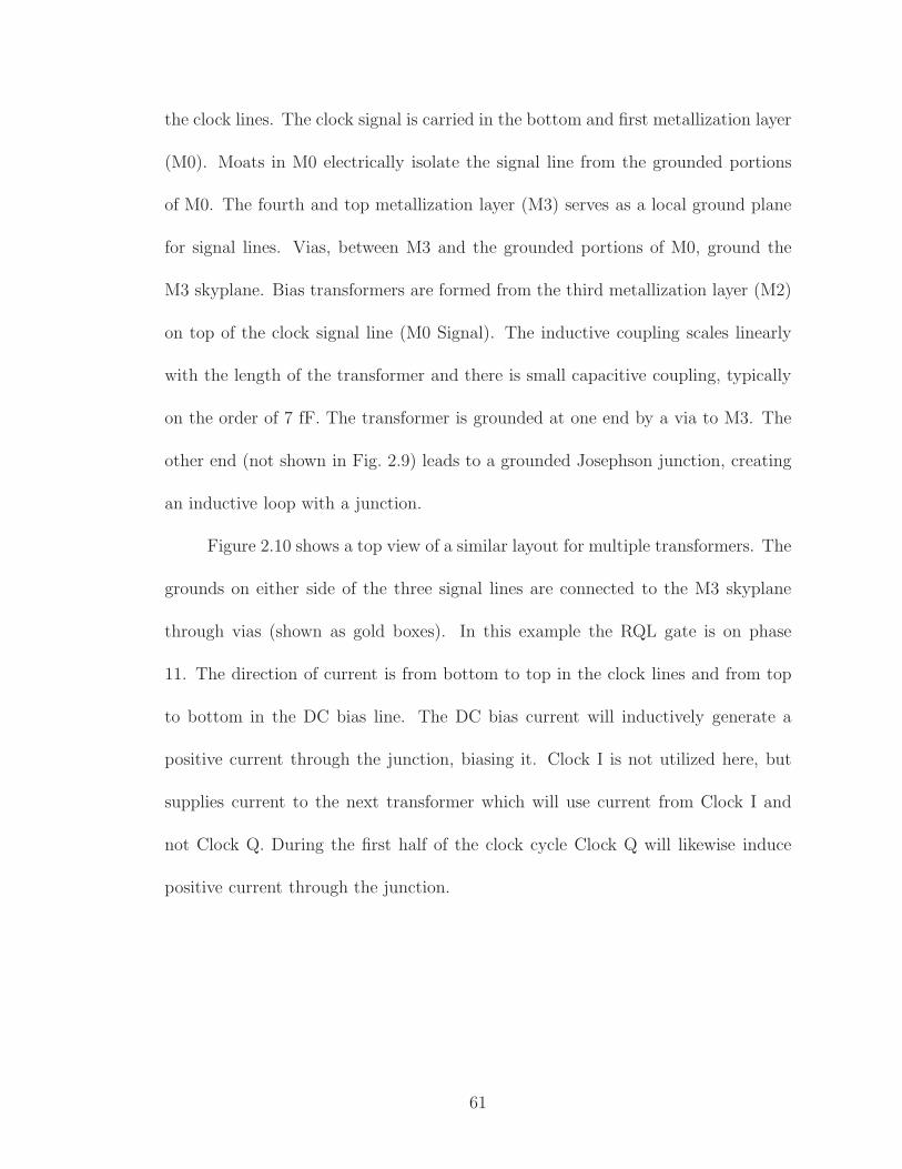
the clock lines. The clock signal is carried in the bottom and first metallization layer
(M0). Moats in M0 electrically isolate the signal line from the grounded portions
of M0. The fourth and top metallization layer (M3) serves as a local ground plane
for signal lines. Vias, between M3 and the grounded portions of M0, ground the
M3 skyplane. Bias transformers are formed from the third metallization layer (M2)
on top of the clock signal line (M0 Signal). The inductive coupling scales linearly
with the length of the transformer and there is small capacitive coupling, typically
on the order of 7 fF. The transformer is grounded at one end by a via to M3. The
other end (not shown in Fig. 2.9) leads to a grounded Josephson junction, creating
an inductive loop with a junction.
Figure 2.10 shows a top view of a similar layout for multiple transformers. The
grounds on either side of the three signal lines are connected to the M3 skyplane
through vias (shown as gold boxes). In this example the RQL gate is on phase
11. The direction of current is from bottom to top in the clock lines and from top
to bottom in the DC bias line. The DC bias current will inductively generate a
positive current through the junction, biasing it. Clock I is not utilized here, but
supplies current to the next transformer which will use current from Clock I and
not Clock Q. During the first half of the clock cycle Clock Q will likewise induce
positive current through the junction.
61

Grou
nd
Grou
nd
Clock
Q
DC
Bias
Clock
I
Figure 2.10: RQL Clock Line Transformer with DC Bias. Top-downdiagram of clockline transformers to supply flux and current bias tojunctions. Two ground planes on the left and right (dark red) connect tothe skyplane (dark blue, visible in outline) though vias (yellow squares).Transformer shown in dark green outline. Currents flow upward in ClockI and Q lines, and downward in the DC Bias line. Flux bias pulls currentout of junction to bias it at −Φ0/2. Clock line pulls current out ofjunction during positive clock phase and pushes current into junctionduring negative clock phase, making this a phase 11 transformer.
2.5.2 Chip Mounting and Cryogenic Environment
Figure 2.11 shows the overall layout of the cryogenic probe used for measure-
ments on the chip. The probe is inserted into a dewar with a 3 inch wide neck which
holds approximately 60 L of liquid helium. (See Fig. 2.11(a).) The liquid helium
is at 4.2 K and the chip is completely submerged in liquid. Figure 2.11(b) shows a
more detailed schematic view of the probe. Above the dewar, female coaxial con-
nectors attach to stainless steel UT-85 coaxial cables which travel down the neck of
the probe to the cold end where they are attached to a printed circuit board (PCB)
62

mount.
The printed circuit board is held by a plastic probe head. The middle of the
probe head is open and exposes 48 or 80 gold contact bumps (depending on the
probe model). 24 or 40 of the bumps are ground contacts. The remaining 24 or
40 contacts connect to the coaxial cables through the PCB. The chip is placed in
contact with these bumps to provide electrical connectivity.
The chip is held in place by a pressure foot. (See Fig. 2.11(b).) Pressure
is applied evenly to the chip by means of the pressure foot. The pressure can be
adjusted by the pressure screw connecting the pressure foot to the bridge. The
bridge is held in place by two screws which are threaded through the bridge and
into the probe head. After the chip is securely in place, two µ-metal shields (not
shown in Fig. 2.11) are attached to the probe head, one over the other, to exclude
magnetic fields from the interior of the probe. Finally, a fiberglass shell is placed
around the assembly and held in place with four screws which are threaded through
the fiberglass shell and into the probe head.
The above generic description cover both the American Cryoprobe Petersen
probe (with 24 signal pads) and the High Precision Devices, Inc., probe (with 40
signal pads). These probes were build-to-order and do not have model numbers.
2.5.3 Experimental Setup
Figure 2.12 shows the overall CAD layout of the Monrovia 20 chip which I
used to test RQL logic gates. This CAD layout was generated by the computer aided
63

Pressure Screw
Bridge Screw Bridge Screw
Bridge
Pressure Foot
3 in
Coaxial Connectors
Probe Neck 36 in
Gold Contact Bumps
Circuit Chip
Probe PCB
Probe Head
Liquid Helium
12 in(b)
(a)
Liquid Helium
Probe
Vacu
um
Vacu
um
Neck
Figure 2.11: Schematic of test probe. (a) The probe used to test chipsis cooled by inserting it into a 60 L dewar of liquid helium. (b) Detailedview of the probe. 40 coaxial connectors at the top of the probe leaddown the probe neck to the probe’s printed circuit board. 80 gold bumpson the PCB serve as pressure contacts to the circuit chip. The chip isheld in place by a pressure foot. The pressure of the foot on the chip canbe adjusted by the pressure screw. The pressure screw is held in placeby the bridge, which is screwed to the probe head by two bridge screws.Figures not to scale.
64

5mm
Monrovia 20 Logic Test (M20LT)Monrovia 20 Power Test (M20SR)
Monrovia 20 Power Splitter (M20PS)
Figure 2.12: Layout of Monrovia 20 RQL chip. This chip contains threeexperimental RQL circuits: the M20LT experiment, which tests the logicbehavior of RQL gates and measures the bit error rate of these gates;the M20SR experiment, which measures the effect of switching junctionson phase and amplitude of the clock signal; and M20PS, which is anexperiment that tests the behavior of the even mode of a Wilkinsonpower splitter (see Chapter 4).
65

design software Cadence.2 There were three experimental circuits on this chip. The
Monrovia 20 Logic Test (M20LT) is the subject of the first experiment here and it
tested the correct logical operation of RQL gates and the bit error rate (BER) of
these gates. The Monrovia 20 Shift Register (M20SR) circuit was used to test the
phase and amplitude modulation of RQL JTLs. The Monrovia 20 Power Splitter
(M20PS) was the subject of a third experiment covered in Chapter 4.
Figure 2.13 shows more detailed views of the layout of the logic circuits in
M20LT. The input is on the left. The logic circuits can be seen in the middle. The
output is on the right, consisting of two large output amplifiers.
Figure 2.14 shows a block diagram for the experimental setup for M20LT and
M20SR. When the bit error rate is tested, the oscilloscope is replaced with an Anritsu
MP1764C BER detector. The data and clock lines return to room temperature
without connecting to the ground on chip. (Each line is inductively coupled to the
circuit.) Return lines are marked with (*) on the block diagram. Output data from
q0 is generated on chip. One clock generator (#1 in figure) (Agilent Technologies
E8275D) generated a synchronization signal for the pattern generator (Anritsu /
Hewitt Packard 70843A). The pattern generator operated at a peak-to-peak voltage
of 0.25 V–2.0 V. The clock signal to the pattern generator was clocked at twice the
speed of the data to provide a return-to-zero (RZ) data input pattern, allowing a
maximum data pattern frequency of 6 GHz RZ. The pattern generator also supplied
a synchronization signal to the oscilloscope (Tektronix TDS 8000 Digital Sampling
Oscilloscope), which always triggered on the beginning of the data input cycle. The
2All layout diagrams in this thesis are taken from the Cadence design environment.
66
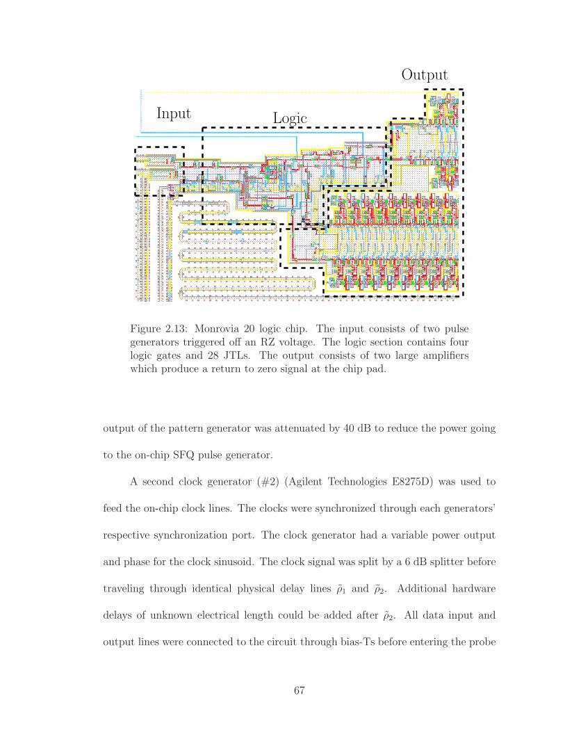
LogicInput
Output
Figure 2.13: Monrovia 20 logic chip. The input consists of two pulsegenerators triggered off an RZ voltage. The logic section contains fourlogic gates and 28 JTLs. The output consists of two large amplifierswhich produce a return to zero signal at the chip pad.
output of the pattern generator was attenuated by 40 dB to reduce the power going
to the on-chip SFQ pulse generator.
A second clock generator (#2) (Agilent Technologies E8275D) was used to
feed the on-chip clock lines. The clocks were synchronized through each generators’
respective synchronization port. The clock generator had a variable power output
and phase for the clock sinusoid. The clock signal was split by a 6 dB splitter before
traveling through identical physical delay lines ρ1 and ρ2. Additional hardware
delays of unknown electrical length could be added after ρ2. All data input and
output lines were connected to the circuit through bias-Ts before entering the probe
67

+
+
+
Attenuator (40 dB)
c1 c1*
a0*a0
c0 c0*
dc0 dc0*
q0Circuit
Junction DC OffsetHardware Delay
Trigger
4.2 K
ρ2
Bias-T
Low-Pass Filter
ρ1
Low Noise Amp
Amplifier DC Source
Sync
DC Data Offset
Oscilloscope
Clock Generator
Pattern Gen.
Clock Generator
#2
#1
Figure 2.14: Experimental setup for timing experiments. Block diagramof the experimental setup for the timing experiments. a0: data input;a0*: data return; c0, c0*, c1, c1*: clock phases and returns; dc0: DCoffset bias; dc0*: offset bias return; q0: experimental output. Lownoise bandpass filters have a cutoff frequency of fC = 1 kHz. Low noiseamplifier is a Miteq LNA with an operation range of 0.518 GHz and a2.5 dB noise floor.
to reduce noise and isolate the circuit from the measurement equipment. Bias-Ts
were also used to isolate the DC offset line, the “Amplifier DC Source” line, and the
“DC Data Offset” line (see Fig. 2.14). These were connected to the chip through
the bias-Ts and were grounded on chip. The output amplifier changed the phase of
the final junctions into an RZ signal and required a DC bias. The DC Data Offset
supplied an overall DC bias to the data input lines.
Each circuit under test contained an on-chip output amplifier that generated a
DC voltage pulse with approximately 2 mV amplitude. The output voltage pattern
is in RZ format, such that the duration of the output pulse is half a clock period. In
68

order to be detectable on the oscilloscope, the output was amplified with a Miteq3
GaAs low-noise amplifier with a frequency range from 0.5–18 GHz, 20 dB gain, and
2.5 dB noise floor. The output voltage was monitored by an oscilloscope, which
could easily detect the 20mV output switching signal.
Figure 2.15 shows typical data waveforms as recorded on the oscilloscope.
Both clock lines were monitored. On the bottom, the output waveform is shown.
Typically, there is a certain amount of cross talk between clock line and data output
lines due to the coupling between lines on the printed circuit board (PCB) used
to make connections to the chip. This crosstalk can be later subtracted from the
signal during data analysis. Each output was fed into the oscilloscope, except the
DC phase offset.
2.6 Experimental Verification
Routing and processing of pulse-based data in RQL is different from what is
used in conventional transistor voltage-based digital logic circuits. While CMOS
logic families are sensitive to rise and hold times, pulse-based logic depends on the
sequence of arrival of pulses. For example, for the RQL AnotB gate, the B pulse
must arrive sufficiently before an A pulse to function properly, even within the same
clock phase. As another example, the AndOr gate sends pulses first to the OR
output, then (if applicable) to AND. In general, in RQL pulses are transient and are
only held at clock phase boundaries. Unlike CMOS transistors, where previous logic
3This is a Miteq ASS4-00501800-25-5P-4 with an operation range of 0.5–18 GHz and a 2.5dB noise floor. All references in this thesis to a Miteq amplifier refer to this model with thisperformance.
69

Voltage
20 mV / div
50 mV / div
50 mV / div
100 mV / div
Time (500 ps / div)
Figure 2.15: Oscilloscope output. Typical output from the TektronixTDS8000 Digital Sampling Oscilloscope while measuring the RQL cir-cuit. Top two rows are input signals returned from chip. The third rowis the two superimposed clock signals returning from chip. The bottomrow is output from the RQL chip, where each peak represents a singlereciprocal SFQ pulse pair. Measurable voltages ranged from 10 mV / divupward, giving 0.1 mV resolution. Measurable times ranged from 50 ps/ division, allowing 1 ps time resolution. Bottom image is a color-inverseof the output, in which the divisions can be seen.
70

operations have lasting effects on output, correct logical operation in RQL depends
on the depth (number of junctions) of each clock phase to ensure synchronized
inputs.
The use of pulse-encoding also affects power dissipation and the bit error
rate. CMOS operates with constant voltage states, while the voltages in RQL are
transient. In both CMOS and RQL, power is expended only during switching, and
then only for digital “one.” CMOS transistors only expend power when switching,
though this has a much different meaning in the technology. RQL junctions switch
for every “one” bit, regardless of previous inputs. CMOS only switches for a change
from “one” to “zero” (or vice versa). For constant inputs this gives a significantly
different number of power dissipating events. For random bits, though, the number
of power-dissipating events in CMOS or RQL will be approximately the same.
To find the bit error rate in RQL, I note that the error condition is very
well defined. Since SFQ pulses are exactly quantized amounts of flux, there is no
threshold voltage as in CMOS. Voltage and current in RQL are defined by the
junctions and are not design parameters as in CMOS. In RQL, errors constitute the
presence of SFQ pulses in a clock period where there should be none, or the absence
of SFQ pulses during a clock period in which they should have been present.
Before designing circuits that used multiple gates, I checked the operation
of individual gates. I also did simulations and then indicated a broad range of
operating margins. Experimental tests (see Chapter 5) have shown that RQL gates
behave much as expected and in some cases actually perform better than expected.
In the remainder of this chapter, I describe three experiments to verify the logical
71
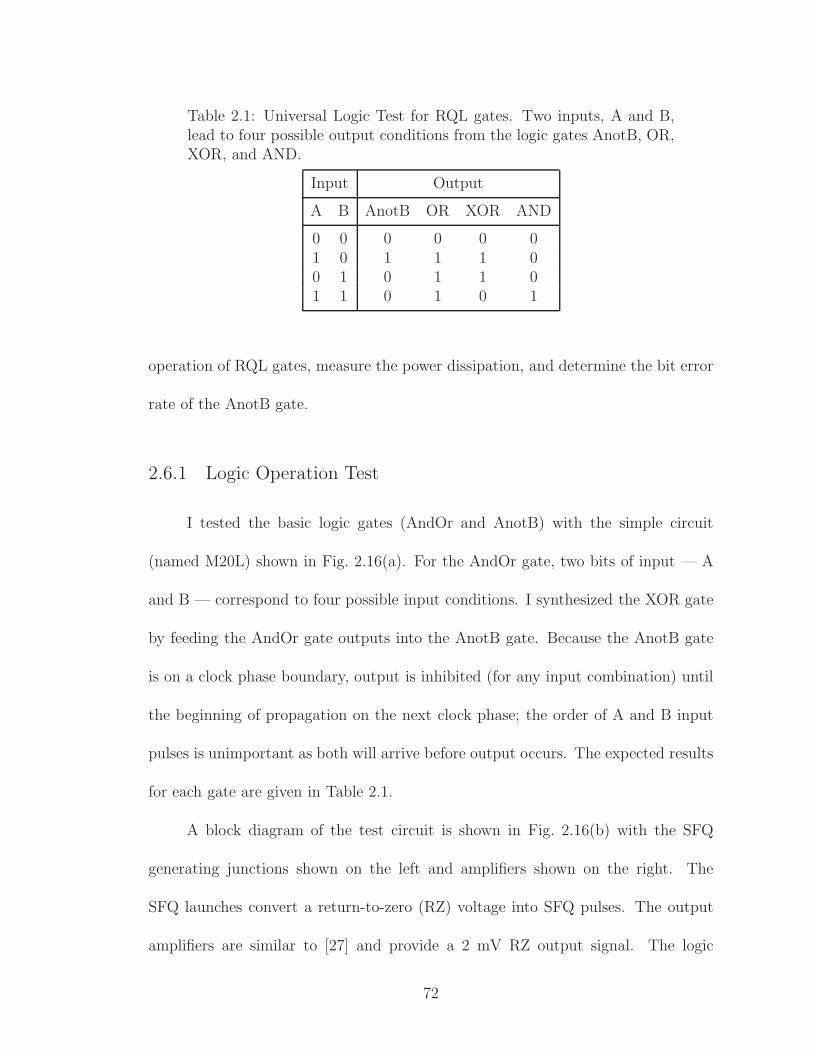
Table 2.1: Universal Logic Test for RQL gates. Two inputs, A and B,lead to four possible output conditions from the logic gates AnotB, OR,XOR, and AND.
Input Output
A B AnotB OR XOR AND
0 0 0 0 0 01 0 1 1 1 00 1 0 1 1 01 1 0 1 0 1
operation of RQL gates, measure the power dissipation, and determine the bit error
rate of the AnotB gate.
2.6.1 Logic Operation Test
I tested the basic logic gates (AndOr and AnotB) with the simple circuit
(named M20L) shown in Fig. 2.16(a). For the AndOr gate, two bits of input — A
and B — correspond to four possible input conditions. I synthesized the XOR gate
by feeding the AndOr gate outputs into the AnotB gate. Because the AnotB gate
is on a clock phase boundary, output is inhibited (for any input combination) until
the beginning of propagation on the next clock phase; the order of A and B input
pulses is unimportant as both will arrive before output occurs. The expected results
for each gate are given in Table 2.1.
A block diagram of the test circuit is shown in Fig. 2.16(b) with the SFQ
generating junctions shown on the left and amplifiers shown on the right. The
SFQ launches convert a return-to-zero (RZ) voltage into SFQ pulses. The output
amplifiers are similar to [27] and provide a 2 mV RZ output signal. The logic
72

circuit was designed to operate at 4.2 K with speeds up to 20 GHz. I used an
Anritsu pattern generator to supply the input pulses and this limited me to 6 GHz.
Figure 2.16(c) shows a representative output of the sampling oscilloscope, which
shows the input on the top two lines and the four outputs on the bottom four lines.
The room-temperature amplifiers invert the signal, causing positive SFQ pulses to
produce downward spikes instead of upward (as on the input). Careful examination
of Fig. 2.16(c) reveals the outputs correspond to the expected results (see Table
2.1).
I also measured the operating margins on the clock power. I found that the
clock power could be varied by ±25% without producing errors, limited by output
amplifiers on the low end. At the high end, an excessive clock amplitude causes
all junctions to switch and generate output, regardless of input. The total latency
through the circuit is one clock cycle. The results shown in Fig. 2.16(c) were per-
formed at a speed of 6 GHz, the upper frequency limit of the pattern generator.
Testing at lower frequencies produced the same logical output, though margins on
the clock power were larger. At lower clock frequencies the switching time of the
junctions becomes a smaller fraction of the clock period. The triangular peaks seen
in Fig. 2.16 become rectangular patterns. However, the logical operation is the
same.
73

Clock 2Clock 1
A
B
XOR
OR
AND
AnotB
Input A
Input B
Voltage (20 mV / div)
A
B
Phase 1 Phase 2 Phase 3 Phase 4 Phase 1
OR
AnotB
AND
Active interconnect −
XOR
AND
XOR
OR
AnotB
Outputs
A
B
AND
XOR
OR
AnotB
c
b
a
6 Gbs Return−to−Zero (1 ns/div)−1
Figure 2.16: Logic Test of Basic RQL Gates. (a) Block diagram of RQLlogic test circuit. Two inputs, A and B, enter from the left. Signals aresplit and sent through five total clock phases, emerging on the left. OneAndOr gate and one AnotB gate shown in Phase 3. One AnotB gateshown in Phase 4. Small blocks represent active interconnect JTL units.Four logic operations are synthesized in this circuit. (b) Cold stagewiring diagram of (a). Two clock lines couple to the junctions in thecircuit. Inputs on right made via two coupled lines which bias junctions.Clocked output amplifiers (different from JTLs) shown on the right. (c)Oscilloscope output of (b) after room temperature low-noise amplifiershave increased the outputs to the millivolt scale. Amplifiers providearbitrary amplification and invert signal. Top two traces are inputs Aand B; bottom four are logical outputs corresponding to above inputs.
74

2.6.2 Clock Power Measurement
To better understand the power dissipation in RQL circuits, I tested a 200-bit
shift register. This device had 1600 Josephson junctions, and is named the Mon-
rovia 20 Shift Register (M20SR). (The shift register is similar to Fig. 2.3 repeated
100 times is sequence. Figure 2.12 shows a layout of the chip.) In RQL circuits the
AC power is delivered on 50Ω microstrip clock lines that return to room temper-
ature without termination on chip. The clock lines are inductively coupled to the
circuit so the Josephson junctions are effectively biased in series. This allows direct
measurement of the amplitude of the clock for both active and inactive circuits. To
make power measurements easier, I designed the shift register with many junctions
and high coupling between the clock line and junctions. This was necessary because
RQL circuits operate with low AC power amplitude and small dissipation in the
junctions; the junctions load the clock line only when they switch to the resistive
state. With high coupling between the junctions and the clock line, more power will
be drawn from the clock line than would regularly be the case. The loss of power
will be reflected in a decreased amplitude of the returning clock signal. This setup,
although it does not have logic gates, will show the change in amplitude clearly. The
clock signal attenuation and phase delay due to the RQL gates scale as the square
of the coupling coefficient k2 and can be minimized by reducing coupling to the
clock line and increasing AC clock power. In real RQL circuits, these parameters
are chosen to allow at most 10% attenuation and less than 2 ps phase delay in a
circuit with 106 Josephson junctions [27].
75

Figure 2.17: Power schematic for RQL delay line: (a) detail schematic;(b) equivalent block diagram, where Z is impedance of RQL gate; (c)equivalent parallel circuit.
AC power losses in Nb microstrips are quite small, on the level of 1% loss
per wavelength up to the gap frequency of 700 GHz [30, 31]. In a practical cir-
cuit with multiple parallel lines, AC losses can be an order of magnitude less than
dynamic power dissipation in the gates. Use of microstrips, as opposed to copla-
nar wave guides, is essential for integration with digital circuits since such circuits
require multiple crossings and couplings to the gates. However, line impedance of
microstrips in general favors sub-micron processes, currently only developed by two
research groups [32, 33].
Figure 2.17 shows the equivalent circuit for a junction that is switching in an
RQL circuit. Switching junctions change the voltage and currents on the clock line
and also affect the impedance of the coupled clock lines. In a simple linear model,
the junction acts as a perfect superconductor before it switches, and it behaves as
a resistor after it switches. Thus, in the case of all digital “ones” we can treat the
junctions as resistors, and the clockline time constant (speed) is simply
τ =√
LcCc = 7.6 fs/µm (2.1)
76

where I have used our clockline geometry with LC = 0.3 pH/µm and CC = 0.29 fF/µm.
For digital “zero” the junction can be treated as an inductance and the clockline
time constant becomes τ ′ =√L′CCC where
L′C = (1− k2)LC + k2LC
Lg
Lg + LT. (2.2)
Here the magnetic coupling constant is k = Lmutual/√LCLT and the inductance
of the RQL gate attached to the bias inductor is Lg. For JTL elements in a shift
register configuration, LJJ1 and L1 are in series, LJJ2 and L2 are in series, and one
finds for the parallel combination of these two series inductors
Lg =(LJJ1 + L1)(LJJ2 + L2)
(LJJ1 + L1) + (LJJ2 + L2)(2.3)
where the junction critical inductances LJJ1 = Φ0/2πIc1, and LJJ2 = Φ0/2πIc2. The
effect of the coupling can be seen in (2.2). The accumulated clock delay though 1600
junctions on the return clock signal on the oscilloscope when data was input and
compared to the delay when no data was input. The measured delay was 1.4±0.2 ps
for the whole chip and was independent of frequency from DC to 6 GHz.
Figure 2.18 shows the results of taking the difference of output clock power
of all “ones” to all “zeros” in the shift register. The measured dissipation is 1.35
times higher than that expected from simulations but three times lower than the
maximum switching power of 2IcΦ0 energy dissipation per digital “one” with average
Ic = 170µA. The power dissipation in RQL circuits with random data can be
approximated as
P =1
3IcΦ0N f, (2.4)
77
where N is the number of junctions in the circuit, Ic is the weighted average critical
current of the junctions, and f is the operational clock frequency. The fraction of
1/3 is due to the behavior of SFQ pulses under AC biasing. Instead of switching at
the critical current Ic, the junctions switch earlier in the clock phase at bias current
Ib < Ic. With increasing phase the junctions switch at larger bias currents, leading
to a slight non-linearity in the relationship between power and frequency, as shown
in Fig. 2.18.
Current Intel i7 processors demand 8 Amps at 12 V, or a power of about
96 W, for approximately 731 million transistors [34], or approximately 130µW per
transistor at approximately 3 GHz. RQL operates at approximately 0.5µW per
junction at twice the speed, as shown in Fig. 2.18. A direct comparison is not
possible because CMOS CPUs by design do not utilize all transistors at once. Some
architectures however minimize the execution time of instructions by utilizing as
many transistors as possible, leading to a 6% increase in speed at the cost of a
16% increase in power consumption [35]. However, an estimate will show the scale
of RQL junction power consumption. RQL logic operations require about four
junctions total. Normalized to logic operation count and clock speed, RQL is still
more than 100 times more power efficient compared to current CMOS technology.
2.6.3 Bit Error Rate
Another key performance metric in testing RQL gates is the bit error rate.
Many mechanisms can lead to failure in a circuit. In many cases, a reduction of clock
78
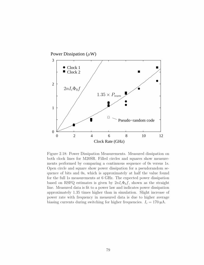
3
2
1
0 0 2 4 6 8 10 12
Clock Rate (GHz)
Pseudo−random code
Clock 2Clock 1
Power Dissipation (µW)
2nIcΦ0f
1.35× Pnum
Figure 2.18: Power Dissipation Measurements. Measured dissipation onboth clock lines for M20SR. Filled circles and squares show measure-ments performed by comparing a continuous sequence of 0s versus 1s.Open circle and square show power dissipation for a pseudorandom se-quence of bits and 0s, which is approximately at half the value foundfor the full 1s measurements at 6 GHz. The expected power dissipationbased on RSFQ estimates is given by 2nIcΦ0f , shown as the straightline. Measured data is fit to a power law and indicates power dissipationapproximately 1.35 times higher than in simulation. Slight increase ofpower rate with frequency in measured data is due to higher averagebiasing currents during switching for higher frequencies. Ic = 170µA.
79

frequency will reduce the rate of errors. In other cases, the failure is independent
of clock speed. For example, the flux bias creates symmetry between positive and
negative SFQ pulses. If the flux bias is too low, pulses fail to propagate and digital
“one” reads as “zero.” High flux bias has the opposite effect, with “zero” reading as
“ones.” In general, excessive current causes junctions to switch even in the absence
of an SFQ pulse.
The AnotB gate is particularly sensitive because it not clocked and as a result
its operating margin depends strongly on the flux bias. I tested an AnotB gate
(see Fig. 2.12) by observing the XOR output of circuit M20LT. At a clock speed of
6 GHz I monitored the XOR output while changing the flux bias near failure. A
32-bit input pattern from an Anritsu MP1763C was split and applied to the inputs
with a 15-bit relative shift between A and B. The XOR output was compared to
the correct pattern with an Anritsu MP1764C error detector. I could operate this
setup for no more than 30 hours due to drift of the synchronization signal between
the generating and measuring units. This set a lower bound on measuring the bit
error rate of about 10−15.
Figure 2.19 shows results I obtained from these measurements. The solid
curves in Fig. 2.19 shows fits of the measured error rate to a Gaussian distribution
p =1
4erfc
(±(I − It)/20√2σI
)
(2.5)
with the two fit parameters It, the current threshold, and σI , the root-mean-squared
noise current. The factor of 1/4 occurs because only “ones” create readout errors and
the factor of 1/20 represents the amount of coupling between the applied flux current
80

-16
-14
-12
-10
-8
-6
-4
-2
0
1 1.5 2 2.5 3
log BER
No errors detected
Flux Bias on AnotB Gate (mA)
10x reduced power
4x reduced power
Figure 2.19: Bit Error Rate for AnotB gate from the M20LT circuit at6 GHz as a function of flux bias Iflux. Very broad operating marginseven for low BER of 10−44. Error bars on the lowest points correspondto counting statics of 4 errors and 5 errors (left and right). No errorsdetected for a period of 30 hours given an error floor below 10−15. Datafit extrapolates to a BER of 10−480 at optimal bias of 1.82 mA. Curvesscaled for decreased size and power.
81

and the resulting flux induced through the junction. For the low bias error (left
curve), I found It = 0.66mA and σI = 1.02µA; for high bias (right), It = 3.04mA
and σI = 1.56µA. No errors were detected for a period of 30 hours at a bias of
about 2.1 mA. This included errors in the chip and the entire measuring apparatus.
At the extrapolated optimal bias point of 1.82 mA the expected extrapolated bit
error rate, based on these measurements, is 10−480. A bit-error rate of 10−44 is
considered the norm in CMOS. From the extrapolation, at a bit error rate of 10−44
the flux bias margins for a nominal flux bias of 1.75 mA will be 30% on either side.
Our extrapolated optimal bit-error rate is phenomenally smaller, and of course it
is a very large extrapolation. Nevertheless, this suggests that this RQL circuit is
performing well.
2.7 Summary
RQL uses positive and negative pairs of SFQ pulses to encode digital data
and performs logic by routing the pulses. This makes logic operations both energy
and size efficient, as well as fast. The AndOr and AnotB gates compose a universal
set. The NDRO gate provides a form of memory. JTLs provide connections between
gates. I found an extrapolated BER of 10−480 at 4.2 K on the output of a synthesized
XOR gate, which is far below the minimum error rate I could measure, 10−15. Noise
current scales as the square root of the Josephson critical current. This gives a
negligible BER of 10−44 with operating margins of ±30% on flux bias.
82

Chapter 3
Combinational Gates
3.1 Introduction
The complexity of modern digital circuits necessitates the use of computer
aided design. Computer aided design also allows for simpler ways to describe digital
circuitry behavior than what would be found from detailed physical simulations,
and yet still encompasses the full range of possible behavior. One standard tool in
common use is VHSIC Hardware Description Language, or VHDL for short. This
standard language (one of only two commonly used by the semiconductor industry)
is used to design nearly every CMOS digital circuit. By casting RQL into the
formalism of VHDL, I can enable the great range of existing design tools and aids
developed for CMOS to be applied to superconducting digital logic.
In the previous chapter, I focused on the behavior of individual junctions and
gates, and described the qualitative timing requirements of RQL gates. In this
chapter I provide a quantitative approach to timing in RQL circuits. First, I derive
an analytic expression for the timing of a single junction. This analytic expression
allows me to understand the self-correcting timing behavior in RQL and the upper
frequency limit of operation. I then fit the analytic equation to simulation data
to produce three parameters which describe the timing behavior of a gate at a
certain frequency. Finally, I build VHDL models using the timing parameters and
83

combinational logic.
3.2 Junction Switching Time under AC Bias Current
In this section I examine the switching of junctions in RQL circuits and find
an analytic equation for the switching time. Using this equation, I show how the
non-linear behavior of the junctions leads to stable, jitter-free pulse propagation. I
also derive a failure condition to determine the maximum operational speed of RQL
circuits. The testing of those models on real RQL circuits is described in Chapter
5.
3.2.1 Analytic Equation for Switching under AC Bias
The switching of junctions in RQL circuits depends on the clock frequency,
clock amplitude, and junction IcRN product. Here I extend the analysis of character-
istic junction switching time for constant biasing to include the case of time-varying
bias currents. In particular, I will assume Ib = AIc sin(ωt), where A is the maxi-
mum bias current in units of Ic, and find the average switching times for the range
of bias conditions. Under the assumption that the junction is overdamped (which
the junctions in my RQL circuits with β ≈ 1 approach), the switching time τ of
Josephson junctions with shunt resistor RN can be expressed as1:
τ =LJ
RN
. (3.1)
1Note that in these RQL circuits, the junctions have been shunted by a resistor RS which ismuch smaller than the junctions’ own resistance R. The junction resistance RN in the RSJ modelis the parallel combination of RS and R, and because RS ≪ R, RS ≈ RN .
84

For Ib ≪ Ic the junction inductance LJ during switching can be approximated as
[6]
LJ =Φ0
2π Ic
φ
Ib/Ic=
Φ0
2π Ic
arcsin(Ib/Ic)
Ib/Ic, (3.2)
where φ(t) is the initial phase across the junction at time t and assuming it has not
already switched. Combining (3.1) and (3.2), the switching time becomes
τ =LJ
RN
=h
2 e IcRN
φ
Ib/Ic=
Φ0
2π
1
IcRN
φ
Ib/Ic= t0
φ
Ib/Ic, (3.3)
where t0 = Φ0/(2π IcRN ) is the characteristic switching time. The quantity t0
depends on the fabrication process though the IcRN product. Table 3.1 compares
IcRN and t0 for different fabrication processes.
Equation (3.3) can also be written as
τ A sin(ωt) = t0 φ. (3.4)
Equation (3.4) implies that the switching time depends on the time t when AC
power biases the junction. In order to account for this we find the average static
bias switching time between the time at the beginning of dynamic switching tin
and the time and the end of dynamic switching tout. This dynamic switching time
τ = tout − tin can be calculated as follows,
1
τ
∫ tout
tin
dt τ A sin(ωt) =1
τ
∫ tout
tin
dt t0 φ(t), (3.5a)
∫ tout
tin
A sin(ωt)dt =1
τ
∫ tout
tin
t0 φ(t)dt = t0 φ, (3.5b)
where φ is the time-average phase across the junction. The time-averaged value of
the phase across the junction is φ ≤ 3 rad to first order [4]. It is useful to express
85
the time in radians of the AC clock to make the results independent of the clock
frequency. Accordingly, I define θ = ωt and thus dθ = ωdt. I then solve for the
output clock phase θout = ωtout as a function of θin = ωtin by noting that Eq. (3.5b)
gives∫ θout
θin
A sin(θ)dθ
ω= 3 t0. (3.6a)
I can then write:
∫ θout
θin
sin θ dθ = cos θin − cos θout =3ω t0A
, (3.6b)
and thus
θout = arccos
[
cos(θin)−3ω t0A
]
. (3.6c)
For overdamped junctions with Ib = Ic the switching time is approximately t =
3ω−1c = 3 t0 [4]. I now define a new quantity
δ = 3ω t0/A. (3.7)
From Eq. (3.6c) we can see that this is the switching time of a DC-biased junction
with bias current Ib = AIc, normalized to the clock period T = 2π/ω. The quantity
δ represents the integral of a normalized voltage over a normalized time period. A
constant bias current A would result in a junction switching over a normalized time
period of θout−θin. As I will show later in this chapter, it turns out that δ is a good
metric of circuit behavior. For example, for δ < 1 SFQ pulses in RQL circuits wait
at phase boundaries, whereas for δ > 1 the pulses can be free-running through the
circuit.
86

Table 3.1: Comparison of different Jc, IcRN and switching time t0 fab-rication technologies.
Hypres HypotheticalFuture Pro-cess
Jc 4.5 10 kA/cm2
IcRN 0.75 1.00 mVt0 0.44 0.33 ps
The amount of change the phase (normalized time) changes from beginning
to the end of switching is ν = θout − θin. Using Eq. (3.6c), the phase delay can be
written as a function of input phase θin
ν(θin) = arccos (cos θin − δ)− θin, θin > 0. (3.8)
Figure 3.1 shows this function for several different clock frequencies. There are a
few interesting things that can be understood from this plot. Notice that as the
frequency increases, so does the relative phase delay ν for any given input phase,
and the curves end at lower and lower input phases. Notice also how the delay
increases rapidly for large θin. The implication is that pulses arriving at sufficiently
large θin will not propagate. Also, note that none of the curves cross, meaning the
timing behavior is uniquely determined. Finally, at low clock speeds the switching
time is far shorter than the clock period and the change in bias current plays only a
small role. That is, at low frequencies δ ≪ 1 and the cos(θ) term in (3.8) dominates.
At higher clock speeds the changing bias current affects the switching time much
more, and in (3.8) the δ term becomes important. As δ → 1 the non-linearity
become more pronounced.
87

0
0.05
0.1
0.15
0.2
0.25
0.3
0.35
0 0.2 0.4 0.6 0.8 1 1.2
ν(θ)[rad/π
]
θ [rad/π]
40 GHz
25 GHz
15 GHz
8 GHz
2 GHz
Figure 3.1: Junction phase delay versus starting junction phase θ. ν(θ)from Eq. (3.8) plotted for clock frequencies of 2, 8, 15, 25, and 40 GHz.Here IcRN = 0.75mV and A = 0.83. ν(θ) is essentially the switchingtime τ normalized to clock frequency, i.e. τ = ν(θ)/2πf . As clock speedsincrease, the delay becomes longer relative to the clock period and thetiming window becomes smaller.
With the delay ν known, the switching time for a single junction can be found
to be τ (t) = ν(ω t)/ω, for a pulse arriving at time t. The switching time for a series
of junctions on the same phase is∑
i τ (ti), where ti+1 = ti + τ(ti).
3.2.2 RQL Timing Stability
The four phase clock/power used in RQL plays a critical role in pulse propaga-
tion. Signal pulses are not free-running in the circuit unlike DC-biased JTLs found
in RSFQ [4], but are instead controlled by the phases of the clock. Here I show that
88

the multi-phase clock provides a self-correcting timing mechanism for RQL gates.
What this means is that small variations in gate delay are corrected by the gate
on the next phase. According to Fig. 3.1, pulses that arrive early cause junctions
to switch slower and the delay between junctions will be longer. Late pulses see a
higher clock bias current and will switch faster. Thus early pulses will arrive later at
the next phase, while late pulses will be accelerated. After traveling through several
clock phases, pulses achieve an equilibrium speed with zero accumulated jitter.
Figure 3.2 illustrates the behavior of a pulse propagating through a JTL with
two junctions on each of four phases. The pulse arrives at JJ1 during the first phase
at 6.8 ps, which is late in the clock cycle and about 5 ps after the junction could
have switched. Because of this, the switching of JJ2, which is also on the A phase
occurs very late in the clock window. As a result, JJ2 has a long switching time,
ending at 11.5 ps. JJ3 is the first junction on the second phase. It receives the SFQ
pulse early in the B clock phase. The delay of the pulse is shorter and leaves earlier.
The delay of the SFQ pulse on the C phase is approximately the same as on the
second phase. The SFQ pulse leaves the C phase before it can begin propagating on
the D phase. When the D phase reaches sufficient bias current at approximately 21
ps, the first junction (JJ7) on the D phase starts to switch. Because the switching
of both junctions JJ7 and JJ8 on the D phase completes within a quarter clock
cycle of the beginning of the clock window, all junctions on later phases will start
to switch at the earliest possible time. Thus, a pulse which arrived late in phase A
is at equilibrium by phase D.
From this example, we can see how the timing stability is enforced by the clock
89

0
0.2
0.4
0.6
0.8
1
1.2
0 5 10 15 20 25 30
I/I c
t [ps]
JJ1JJ2
JJ3JJ4
JJ5JJ6
JJ7JJ8
A B C D
Figure 3.2: Self-correcting timing mechanism of RQL simulated for aclock frequency of 40 GHz and IcRN = 0.75mV. Four sinusoidal clockphases are shown as a function of time. Eight junctions, two per phase,are represented as different hatched regions beneath their respectivecurves. The area associated with each junction is equal and defines thebeginning and end of the switching process. Each junction must switchsequentially. A–D show the earliest possible switching time for eachjunction, with the arrows indicating how long after this time switchingactually starts. Arrows labeled JJ1–JJ8 show the length of switchingtime. The delay is about 5 ps for junction A while later delays decreaseas the pulse travels through the JTL. Note that switching events nearthe peak of the bias current occur faster.
90

phase boundaries. Equation (3.8) gives the delay of an SFQ pulse as a function of
the input phase. At a clock boundary, the delay can be expressed in terms of the
input phase at one clock phase and the output phase to the next clock phase. Figure
3.3 shows a plot of tout (the actual output time relative to the beginning of the clock
cycle, not the delay time τ) versus the input phase. Point a in the figure is the
stable timing point. Pulses arriving earlier are delayed relative to the leading edge
of the sinusoid whereas later pulses are accelerated. Notice however, if pulses arrive
late enough in the cycle, they will be slowed down. This leads to the stable timing
window ending at point b in the figure. At this meta-stable timing point any small
decrease in speed will cause greater delays and a slight increase in speed will cause
smaller delays. Pulses that are so late that they arrive after point b will slow down
until they reach point c, the timing window cut-off point, after which pulses fail to
propagate.
Although it is not obvious from Fig. 3.3 which is drawn for δ = 1.216, for
slow clock speeds (δ < 1) the stable timing point coincides with the origin and
the metastable point does not exist. In this case, all pulses arriving before the
cut-off point c are sped up. An important advantage of the RQL timing scheme is
that timing errors can be corrected by decreasing the clock frequency. This is not
always true for RSFQ where fixed hardware delays can cause failure at low or high
frequencies [36].
91
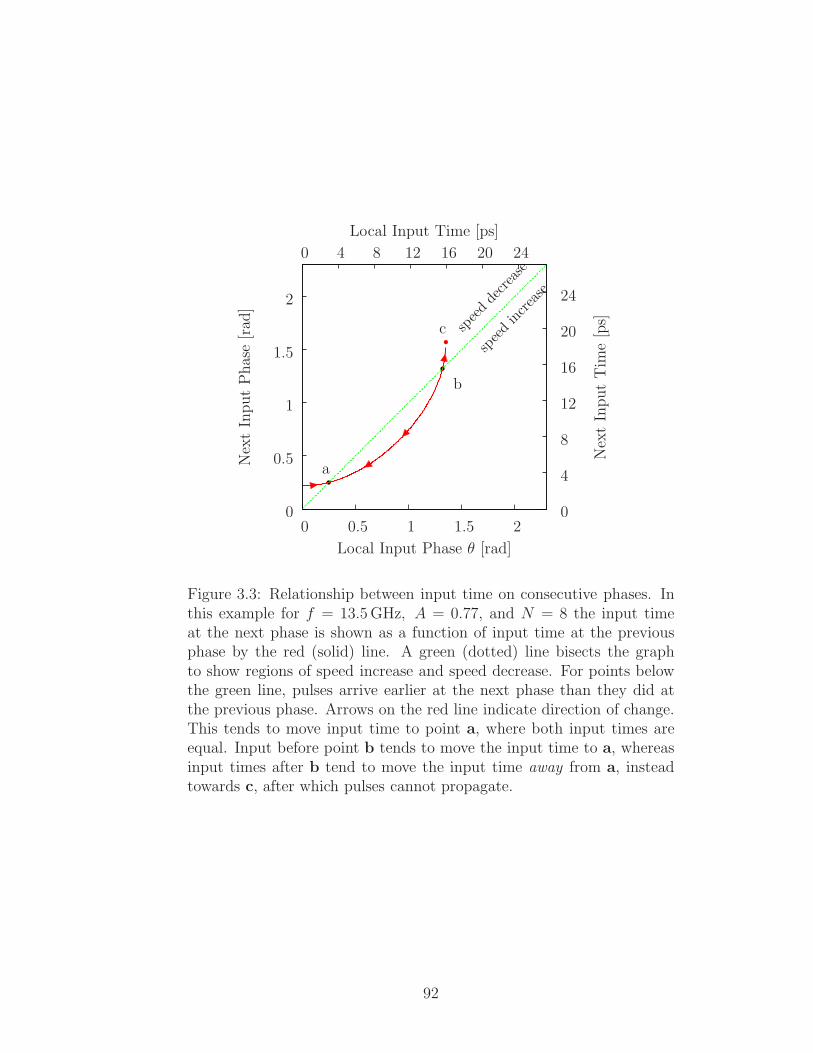
0
0.5
1
1.5
2
0 0.5 1 1.5 20
4
8
12
16
20
24
0 4 8 12 16 20 24NextInputPhase[rad
]
NextInputTim
e[ps]
Local Input Phase θ [rad]
Local Input Time [ps]
c
b
a
speeddecrease
speedincrease
Figure 3.3: Relationship between input time on consecutive phases. Inthis example for f = 13.5GHz, A = 0.77, and N = 8 the input timeat the next phase is shown as a function of input time at the previousphase by the red (solid) line. A green (dotted) line bisects the graphto show regions of speed increase and speed decrease. For points belowthe green line, pulses arrive earlier at the next phase than they did atthe previous phase. Arrows on the red line indicate direction of change.This tends to move input time to point a, where both input times areequal. Input before point b tends to move the input time to a, whereasinput times after b tend to move the input time away from a, insteadtowards c, after which pulses cannot propagate.
92

3.2.3 Frequency Limit
The analytic timing model discussed in the previous two sections allows me to
predict the frequency limits of operation for RQL circuits. As can be seen from Fig.
3.4, as the frequency increases the stable timing window gets smaller. Eventually
the stable and meta-stable timing points converge, corresponding to the maximum
operational frequency. At this limiting frequency, the minimum delay is equal to
one quarter the clock period.
Figure 3.4 shows the relationship between the timing window and the stable
and meta-stable timing points. In the figure, the timing window is marked by the
empty box on the left and solid box on the right. For δ ≤ 1 the stable timing window
extends from θ = 0 to θ = θc and no stable or meta-stable timing points exist. All
pulses within the timing window will move towards t = 0 while pulses outside the
timing window will fail to propagate. For δ > 1 the stable timing window extends
from θs, the input phase corresponding to the stable timing point, to θms, the input
phase corresponding to the metastable timing point — that is, the clock phase θ of
points a and b in Fig. 3.3, respectively. In Fig. 3.4, all stable and metastable timing
points correspond to an output phase delay of ν = π/2 because this represents a
delay of one quarter clock cycle. Pulses arriving earlier than θs will be slowed down
and move towards t = θs/ω. Pulses arriving later than θms will be slowed down as
well until they are delayed to the point they can no longer propagate.
Equation (3.8) was derived from the behavior of a single junction. We can
extend the equation to cover multiple junctions in a clock phase by changing δ → Nδ,
93

0
0.1
0.2
0.3
0.4
0.5
0.6
0.7
0 0.2 0.4 0.6 0.8 1
ν(θ)[rad/π
]
θ [rad/π]
16.2 GHz
13.5 GHz
8 GHz
4 GHz
1 GHz
17 GHz
equilibrium
Figure 3.4: Switching delay ν versus input phase for different clockfrequencies. Similar to Figure 3.1, this figure shows (3.8) plotted forIcRN = 0.75mV, A = 0.83, and N = 8. Open boxes show stable timingpoints, filled boxed show metastable timing points. Metastable timingpoints lie along the line ν = π−θ until they reach a maximum of ν = π/2.Both stable and metastable timing points then lie at the intersection ofν(θ) and ν = π/2. The limiting case for 17 GHz is shown as the topcurve.
where N is the number of junctions in a given phase. The fastest propagation is at
the minimum of the timing equation. We find the input phase θmin that gives the
shortest delay by setting
dν(θ)
dθ
∣∣∣θ=θmin
=sin θmin
√
1− (cos θmin − δ)2− 1 = 0, (3.9)
and thus the input phase at minimum delay is
θmin = arccosδ
2. (3.10)
94

Substituting (3.10) into (3.8), I can write for the minimum delay condition:
ν(θmin) = arccos (cos θmin − δ)− θmin =π
2, (3.11a)
arccos
(δ
2− δ
)
− arccos
(δ
2
)
=π
2. (3.11b)
Equation (3.11b) has a solution at δ =√2. Using the definition of δ then gives the
following relationship for the maximum expected possible frequency
fmax =A
3√2πNt0
. (3.12)
fmax can be made large by choosing short SFQ pulses (i.e. small t0, which can be
obtained by choosing large IcRN) and a small number of junctions per phase N .
I can draw a number of important conclusions about timing in RQL circuits.
First, at f = fmax the metastable timing point is at θmin = π/4. Second, the value
of δ is limited to 0 < δ < 2. For δ < 1, pulses are clock-limited, propagating through
each clock phase and waiting at the phase boundary. For 1 < δ <√2 pulses travel
ballistically, traveling through several clock phases before reaching equilibrium. For
δ >√2 pulses propagate slower than the clock signal, and for δ > 2 no pulses can
propagate. Using the values for the Hypres process given in Table 3.1 and choosing
A = 0.83 and N = 8, I estimate the maximum clock frequency for RQL circuits at
about 17 GHz (see Fig. 3.4).
3.3 Timing Extraction from Simulation
WRSpice2 uses the RSJ model of Josephson junctions. The capacitor behaves
linearly. The resistor is non-linear and uses a piecewise linear model of the resistance,
2http://www.wrcad.com/manual/wrsmanual/wrsmanual.html
95

using one value of resistance Rs for currents through the junction I < Ic, and another
value of resistance Rq for currents through the junction I > Ic. The junction itself
is modeled following the two Josephson equations (1.34) and (1.35), additionally
recording the phase of the junction.
The time-domain analysis of the circuit is done in small time steps,3 identical
to the solution method of the original open-source SPICE3 program [37] on which
WRSpice is based. At each time step the circuit is represented as a sparse matrix G
relating the voltages at every node to the currents between nodes, where GV = I.
Non-linear elements, such as Josephson junctions, are represented in differential or
integral form4. SPICE solves the ordinary differential equation using the Newton-
Raphson iterative method. When convergence is achieved the simulator moves on
to the next time step.
WRSpice takes ASCII-format netlist files. To perform my simulations, I first
used Cadence Virtuoso schematic editor to layout the circuits shown in Fig. 3.7
using dummy value for the relevant circuit parameters (clock speed, input time). I
generated a separate netlist for each gate (two for the AndOr gate, one for each of the
two outputs). Then, using a perl computer language script to replace dummy values
with real values, I had the simulations done and results analyzed automatically. (See
Appendix B for details on the simulations.)
The analytic timing expression (3.8) can be applied to real gates. However,
I had to make some assumptions that were not necessarily well justified for RQL
3http://bwrc.eecs.berkeley.edu/classes/icbook/spice/4http://www.nutwooduk.co.uk/pdf/Issue82.PDF#page=27
96

circuits. More accurate results can be obtained by full physical simulation of the
junction behavior. The analytic timing model can then be fit to the simulation to
obtain a relationship between input phase and output phase. To do this, in this
section I first define a delay time in terms of measurable (physical) quantities. I
then define a consistent path though a gate to which this delay applies. Finally, I
discuss the physical simulation of gates in an appropriate circuit to generate results
which I then fit using the analytic model.
The phase φ across a junction is the natural coordinate describing the switching
of a junction. In the mechanical pendulum analog of a junction, φ is the angular
position of the pendulum. In the washboard potential, if the particle is moving from
one local minimum to the next, then at any time the phase is clearly on one or the
other side of the potential barrier. I will assume that φ = 0 initially and that after
an SFQ pulse φ = 2π. I then define φc = (1 − e−1) × 2π as the transition point.
For the reciprocal pulse the transitions point is φ′c = 2π − φc. This choice of φc is
somewhat arbitrary, so I leave φc as a variable and need to check that my particular
choice does not impact critical results. (See Appendix B.)
Figure 3.5 shows the simulated behavior of the phase difference across of two
junctions in a JTL that are connected in series and switch on the same clock phase.
From this plot, I define the points tin and tout as the time when the JJ1 and JJ2
junction phases respectively cross the value φc. I then calculate the difference ∆t =
tout− tin as the delay in the two-junction circuit. In normalized units of clock phase,
I can define θin = ωtin and ∆θ = ω∆t for clock frequency ω and clock amplitude
A = Ib/Ic. I preformed multiple simulations for different values of clock frequency
97

0
0.2
0.4
0.6
0.8
1
1.2
100 110 120 130 140 150
φ[rad
/(2π
)]
t [ps]
tin tout φc
Figure 3.5: Spice simulation of the phases of two sequential junctionsin a JTL during switching. The phase φ of junction JJ1 (solid curve)and JJ2 (dashed curve) on the same clock phase is plotted as a functionof time. The phase of JJ1 crosses φc at tin, which marks tin and thebeginning of the switching time for JJ2. When the phase of JJ2 crossesφc at tout the switching time ends. The arrow in the figure indicates thelength of the switching time.
and clock amplitude to generate a set of timing data for a gate or logic operation.
The gate delay is defined as the time between arrival of the input pulse at the
input junction of the gate and the arrival of the output pulse at the input junction
to the next gate. Figure 3.6 shows this concept for the AndOr gate. A pulse arrives
at junction b, causing it to switch. Later, junction c at the input of the next gate
switches. For consistency I demand that the time of output at one gate is the same
as the time of input at the following gate. That is, I define the data path to extend
past the conceptual boundary of the logic gate and into the next circuit element
98

b d
ca
ANDOR GATE
Figure 3.6: Data path through AndOr gate. The AndOr and four JTLs,one each at each input and output, is shown schematically with fourjunctions of interest labeled a – d. The junctions a and b, enclosedin the dashed box, which are physically part of the AndOr gate. Thisfigure illustrates the data path through the gate for “or.” The data pathis shown in black; the inactive path is shown in grey. For “or” the datapath starts with junction b and ends with junction c, even though c isoutside the physical boundaries of the AndOr gate.
(see Fig. 3.6).
3.3.1 Fitting Simulation Results
With the delay and data path defined, I proceeded to simulate the gate be-
havior in WRSpice. Because the timing parameters should not depend on the test
bench (the circuit schematic which is intended to be representative of any generic
circuit), I must choose a test bench which generates representative simulation re-
sults for junction switching behavior. One of the test circuits I used is shown in
Figure 3.7(a). In the circuit, JTL stages are inserted in different numbers for differ-
ent clock speeds. The number of JTL stages was scaled to the frequency to cause
failure (non-switching) of one of the junctions in one of the last units. As the SFQ
99

c
d
Single JTL
Phase 1 Phase 1
a
b
AB
N JTLs, 2N JJs (single phase)
(b)
(a)
Figure 3.7: Circuits used to extract RQL timing results from spice sim-ulations. Schematics of two circuits used for timing extraction simula-tions. Input is on the left and signals are terminated in the circuit byresistors to ground on right. (a) A series of JTLs on a single phase leadto a resistor to prevent reflection of the SFQ pulse. The total number Nof JTLs in series was scaled to the frequency. High frequencies containedfewer JTLs, while lower frequencies contained as many as forty JTLs ona single phase. (b) Gate timing extraction with AndOr gate as a repre-sentative example. Two inputs lead to two JTLs labeled a and b, whichthen output to a logic gate. The two gate outputs lead to two furtherJTLs, c and d. Output from JTLs c and d terminate in resistors. Othergates use a different combination of JTLs a, b, c, and d.
pulses pass each JTL stage in sequence, it will generate one timing simulation point
per stage.
Figure 3.7(b) shows the test circuit for the gates. I chose the AndOr gate as a
representative gate because it has two inputs and two outputs. The basic simulation
approach is the same for all gates although one must make some modifications for
certain gates. For example, for the splitter, input JTL b is omitted. As another
example, for the AnotB and Set-Reset gates, output JTL d is omitted. Each sim-
100

ulation provides one timing data point and with multiple simulations, I varied the
input phase θin to give a spread of timing results (phase is a function of time) which
I then analyzed. Details of the simulation routine I used are found in Appendix B.
Using a perl script I analyzed the simulation output and recorded the time
pairs at which successive junctions in a data path crossed the critical phase value
φc. Linear interpolation was used to estimate the time of crossing based on the
immediately previous and following points. The delays νfit for a given input phase
θ were then fit to:
νfit(θ) = α1 α3 [arccos (cos (α2 θ)− δ/α3)− α2 θ] , (3.13)
where α1, α2, α3 are of fitting parameters and ν is the delay in radians. This is a
modified form of our expected timing (3.8) and this choice of fitting parameters
removes correlation between them. Ideally, these parameters would all be unity.
Table 3.2 shows a portion of the full timing table I constructed from simulations
of the JTL. The full table can be found in Appendix B. The first thing to notice
about the Table is that α1 and α2 are close to 1, as expected. These two parameters
simply scale the input phase and phase delay. α3 is close to 1 for higher frequencies,
but is noticeably different from 1 for low frequencies. In fact, the general trend is
that all α parameters get closer to 1 as the frequency is increased. α3 is a scaling
parameter for the curvature and we expect it to be less close to 1 than the other
parameters due to the varying bias conditions in real circuits. Because the timing in
much less sensitive to the delay at low frequencies, the divergence from 1 for the α
parameters at lower frequencies is of lesser consequence. The additional information
101
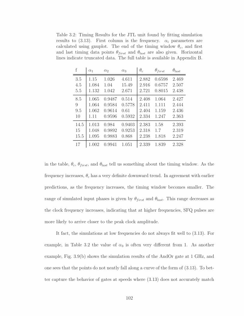
Table 3.2: Timing Results for the JTL unit found by fitting simulationresults to (3.13). First column is the frequency. αi parameters arecalculated using gnuplot. The end of the timing window θc, and firstand last timing data points θfirst and θlast are also given. Horizontallines indicate truncated data. The full table is available in Appendix B.
f α1 α2 α3 θc θfirst θlast
3.5 1.15 1.026 4.611 2.882 0.6598 2.4694.5 1.084 1.04 15.49 2.916 0.6757 2.5075.5 1.132 1.042 2.671 2.721 0.8015 2.438
8.5 1.065 0.9487 0.514 2.408 1.064 2.4279 1.064 0.9584 0.5778 2.411 1.111 2.4449.5 1.062 0.9614 0.61 2.404 1.159 2.43610 1.11 0.9596 0.5932 2.334 1.247 2.363
14.5 1.013 0.984 0.9403 2.383 1.58 2.39315 1.048 0.9892 0.9253 2.318 1.7 2.31915.5 1.095 0.9883 0.868 2.238 1.818 2.247
17 1.002 0.9941 1.051 2.339 1.839 2.328
in the table, θc, θfirst, and θlast tell us something about the timing window. As the
frequency increases, θc has a very definite downward trend. In agreement with earlier
predictions, as the frequency increases, the timing window becomes smaller. The
range of simulated input phases is given by θfirst and θlast. This range decreases as
the clock frequency increases, indicating that at higher frequencies, SFQ pulses are
more likely to arrive closer to the peak clock amplitude.
It fact, the simulations at low frequencies do not always fit well to (3.13). For
example, in Table 3.2 the value of α3 is often very different from 1. As another
example, Fig. 3.9(b) shows the simulation results of the AndOr gate at 1 GHz, and
one sees that the points do not neatly fall along a curve of the form of (3.13). To bet-
ter capture the behavior of gates at speeds where (3.13) does not accurately match
102

the simulation results, I also fit the simulation results between the first recorded
input phase θfirst and the last recorded input phase θlast to a piecewise polynomial
equation
pfit(θ) = ((α11θ + α12)θ + α13)︸ ︷︷ ︸
polynomial
Θ(θ − w) + ((α21θ + α22)θ + α23)︸ ︷︷ ︸
polynomial
Θ(w − θ), (3.14)
where Θ(x) is the step function defined by Θ(x) = 1 for x > 1 and Θ(x) = 0
for x < 1, w = (θfirst + θlast)/2 is the phase between the first and last recorded
input phases, and the αij are fitting parameters — unrelated to the αi parameters
in (3.13).
Figure 3.8 shows the simulated delay points for the JTL at a frequency of 16
GHz and clock amplitude A = 0.83. The fit to (3.13) is shown by the green dashed
curve. We can see that it is similar to the prediction from (3.8) using the nominal
circuit parameters (red solid curve) This corresponds to α1 = α2 = α3 = 1. More
importantly, we see that the points are close to the fit. In Fig 3.8, I also show
the polynomial fit as a blue dashed curve. The polynomial fit parameter values
are recorded in Table B.2 (see Appendix B, page 229). The polynomial fit is only
applicable for θfirst < θ < θlast. Outside this range the fit to (3.13) gives better
results.
If (3.8) is correct, then ideally all the αi parameters should be close to unity.
Clearly, this is not always the case. Also, in certain cases the fit to (3.13) gives large
errors, especially at higher frequencies where fewer data points are available and
at very low frequencies where the simulation behavior indicates a stepwise timing
function. In such cases, the piecewise polynomial fit produces better results.
103

0
0.2
0.4
0.6
0.8
1
0 0.5 1 1.5 2 2.50
1
2
3
4
5
6
7
8
9
100 3 6 9 12 15 18 21 24 27
OutputPhaseDelay
[rad
]
OutputTim
eDelay
[ps]
Input Phase [rad]
Input Time [ps]
a1 = 1.04914
a2 = 0.981119
a3 = 0.896482
f = 16 GHz
A = 0.83
N = 2
NominalFit
Polyfit
Figure 3.8: Fit of delay equation to simulated switching times for f =16GHz, A = 0.83, N = 2. Purple data points come from simulation andanalysis of the circuit shown in Figure 3.7(a). The nominal behavior (redcurve) matches the data closely. The fit to the analytic equation (greendashed curve) is close to the nominal behavior. The fit parameters α1,α2, and α3 are shown on the figure. The fit to the piecewise polynomialfunction fits well within the region where data is available but divergesstrongly from the other fits outside this region.
Logic gates that are not directly biased by the ac clock signal will not neces-
sarily have a timing response that is similar to clock-powered JTLs. In contrast to
a JTL, one should expect these logic gates to exhibit behavior that diverges from
the analytic timing equation (3.13). Figure 3.9 shows results for the AndOr gate
outputting an OR-pulse at f = 12GHz (Fig. 3.9(a)) and the AnotB gate generating
output at f = 1GHz (Fig. 3.9(b)). For the AndOr gate the analytic equation (green
dashed curve) works surprisingly well even for an unpowered junction. The fitting
104

parameters α1, α2, α3 show some divergence from nominal values of one, although
for practical purposes the fit is excellent.
Figure 3.9(a) shows an example of poor fitting for the AndOr gate at 1 GHz.
The behavior departs strongly from (3.13). For the AnotB gate (see Fig. 3.9(b))
the analytic fit (green dashed) shows significant errors. As can be seen, the timing
response is more like a step function than the best fit to the analytic timing equation.
Although it is worth noting that the median switching time is close to the value
predicted by the nominal case, the data points lie fairly close to the red curve
over the region of interest. A piecewise polynomial fit better represents the timing
behavior in this case. At low frequencies, early pulses will get stuck at a logic gate,
as there is very little current leaking in to the gate from either adjacent JTL unit
(see Chapter 2). The pulse must wait until the local bias current is sufficiently
high, at which time the switching event follows almost immediately. This behavior
can be seen in the figure as a steady increase in the phase delay for shorter input
delays. As a practical matter in circuit design, errors for low frequencies are of little
importance. For δ ≪ 1 the latency is much less than the clock period and pulses
will not fail due to timing issues. For frequencies of interest, where δ ≈ 1, the fits
work well.
Using Table 3.2 I can generate plots of the fitted equation νfit(θ) for different
values of frequency. For example, Fig. 3.10 shows timing curves for different clock
frequencies that required different α parameters. As in the purely analytic case the
trend is toward longer phase delays for higher frequencies and the curves do not
cross, as one would expect for real physical processes.
105
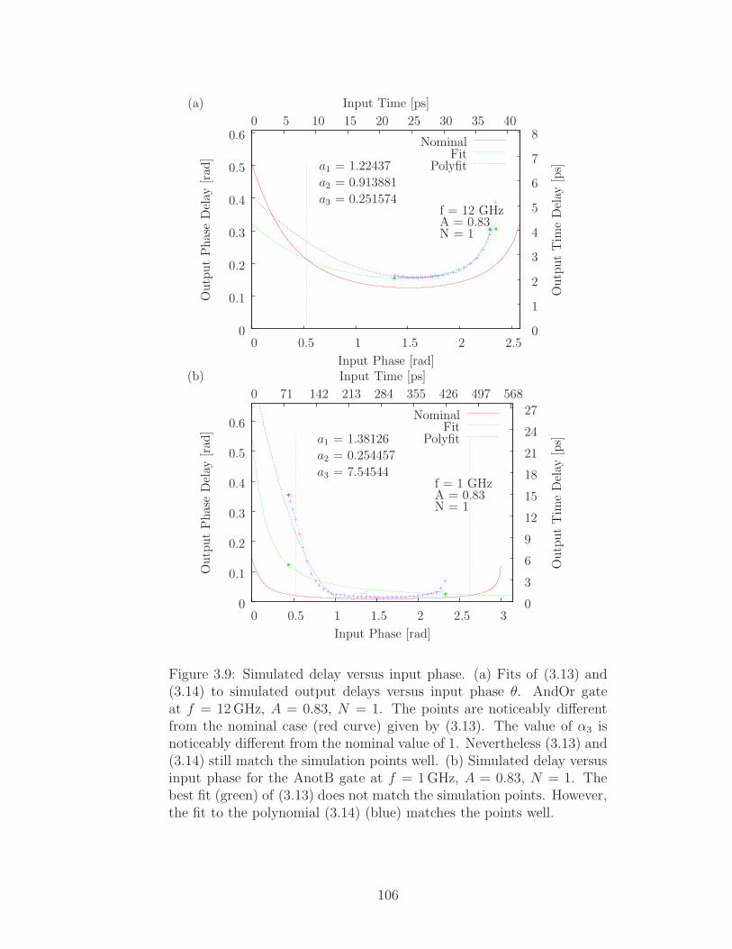
0
0.1
0.2
0.3
0.4
0.5
0.6
0 0.5 1 1.5 2 2.50
1
2
3
4
5
6
7
80 5 10 15 20 25 30 35 40
OutputPhaseDelay
[rad
]
OutputTim
eDelay
[ps]
Input Phase [rad]
Input Time [ps](a)
a1 = 1.22437
a2 = 0.913881
a3 = 0.251574f = 12 GHzA = 0.83N = 1
NominalFit
Polyfit
0
0.1
0.2
0.3
0.4
0.5
0.6
0 0.5 1 1.5 2 2.5 30
3
6
9
12
15
18
21
24
27
0 71 142 213 284 355 426 497 568
OutputPhaseDelay
[rad
]
OutputTim
eDelay
[ps]
Input Phase [rad]
Input Time [ps](b)
a1 = 1.38126
a2 = 0.254457
a3 = 7.54544f = 1 GHzA = 0.83N = 1
NominalFit
Polyfit
Figure 3.9: Simulated delay versus input phase. (a) Fits of (3.13) and(3.14) to simulated output delays versus input phase θ. AndOr gateat f = 12GHz, A = 0.83, N = 1. The points are noticeably differentfrom the nominal case (red curve) given by (3.13). The value of α3 isnoticeably different from the nominal value of 1. Nevertheless (3.13) and(3.14) still match the simulation points well. (b) Simulated delay versusinput phase for the AnotB gate at f = 1GHz, A = 0.83, N = 1. Thebest fit (green) of (3.13) does not match the simulation points. However,the fit to the polynomial (3.14) (blue) matches the points well.
106

0
0.1
0.2
0.3
0.4
0.5
0.6
0.7
0.8
1 1.5 2 2.5
OutputDelay
[rad
]
Input Phase [rad]
1 GHz2.5 GHz3.5 GHz6 GHz10 GHz
10.5 GHz13 GHz
Figure 3.10: Comparison of Extracted Timing Curves. The fitted phasedelay (3.13) is plotted using appropriate values for α1, α2, and α3 forseven different frequencies from 1 GHz to 13.5 GHz. These curves havethe same properties as the curves shown in Figure 3.1: the curves do notcross, low frequency curves are nearly flat, as the frequency increases,so does the output phase delay, and the endpoints of the curves moveinward as the frequency increases.
It would be impractical to tabulate fitting parameters for all frequencies. In-
stead, I used linear interpolation in the frequency range between simulated frequen-
cies. Figure 3.11 shows that linear interpolation between 10 GHz and 15 GHz fits
well to the simulated 13 GHz data. The interpolated curves for both the analytic
and piecewise polynomial fits match the data very well. The only drawback of inter-
polation is that it is limited by the end of the timing curve for the higher frequency.
107

0.2
0.3
0.4
0.5
0.6
0.7
0.8
0.9
1.5 1.6 1.7 1.8 1.9 2 2.1 2.2 2.3 2.4
PhaseDelay
ν fit(θ)[rad
]
Input Phase θ [rad]
Interpolation between Analytic Timing Equation Fits(a)
15 GHz
10 GHz
13 GHz
0.2
0.3
0.4
0.5
0.6
0.7
0.8
0.9
1.5 1.6 1.7 1.8 1.9 2 2.1 2.2 2.3 2.4
PhaseDelay
p fit(θ)[rad
]
Input Phase θ [rad]
Interpolation between Polynomial Fits(b)
15 GHz
10 GHz
13 GHz
Figure 3.11: Simulated timing data for the JTL at 13 GHz (red soliddots) and plots of (3.13) and (3.14) for the JTL at 10 GHz and 15 GHz(green dashed curves). Both interpolations work well except at the limitsof the region of interest, where the circuit is near failure already. Thecurve passing through the data points (red solid curve) is not a fit of(3.13) or (3.14) to the data but a linear interpolation of the functionsto 13 GHz. Interpolation works well except at the end of the windowhigher frequencies.
108

3.4 VHDL Models for RQL Gates
In this section I explain an RQL gate model that I implemented in VHDL5,
a widely-used standard for timing design in the semiconductor industry. The mod-
els describe logic functions, timing behavior, and failure mechanisms. With these
VHDL models, I can use semiconductor timing design techniques. VHDL uses
multi-valued signals (called a class in VHDL) and determines the times at which
transitions between the allowed values occur. I used the existing std ulogic class6, a
common CMOS class which I found was appropriate for use with RQL circuits.
3.4.1 Behavior of VHDL Models
The VHDL models of RQL circuits that I built start from a model of the AC
clock. The AC sinusoid is partitioned into three equal parts as shown in Figure
3.12. “High” and “Low” are above half maximum or below negative half maximum,
respectively, and otherwise the clock is “Off.” A positive pulse arriving during High
will over-bias the junction and generate a new pulse; likewise for Low and a negative
pulse. Insufficient bias during Off means pulses do not propagate and wait for the
next High or Low region. This combination of “High,” “Low,” and “Off” sectioning
gives a model for the clock signal identical to the std ulogic model for CMOS in
VHDL.
To simulate the behavior of RQL circuits and gates I developed a VHDL simu-
lation package. The VHDL model contains the pulse-based logic of RQL, calculates
5IEEE 1076-2008: VHSIC Hardware Description Language6IEEE 1164-1993: IEEE Standard Multivalue Logic System for VHDL Model Interoperability
109

-1
-0.5
0
0.5
1
0 10 20 30 40 50 60
0 1 2 3 4 5 6 7 8 9 10 11 12 13 14 15 16 17 18
BiasCurrent[I/I
c]
Time [ps]
Clock Phase [rad× (π/6)]
HIGH OFF LOW OFF HIGH
Figure 3.12: Timing model for RQL clock. The AC clock is partitionedinto three logical segments. For |sin θ| < 1/2 the clock is “Off,” dur-ing which pulse propagation is forbidden because of low bias. Likewise,“High” and “Low” are defined for sin θ > 1/2 and sin θ < −1/2, respec-tively, and only allow positive or negative pulses to propagate.
the delay from the analytic equation, and tracks energy dissipation, switching events,
and approximate circuit size. The VHDL model is scalable for different fabrication
processes. Table 3.3 shows the basic elements of the VHDL model.
Global parameters include IcRN , the junction energy scale set by the fabrica-
tion process. Clock frequency ω is the chosen clock frequency for operation, identical
for all JTL units in the same circuit. A is the clock amplitude, a quantity important
for the timing behavior. βc is the Stewart-McCumber parameter which can be cho-
sen for a particular design, and effectively changes the IcRN product. Jtotal is the
total junction count of the chip, which serves as a metric for the area of the circuit.
110

Table 3.3: Global VHDL Quantities. The interaction between gates andthe overall behavior of the circuit is governed by certain global inputsand signals. Global elements are inputs which allow the code to scale toany process, as well as record operation metrics such as power. Signalsspecify how the output of one gate becomes the input of the next, aswell as carry clock phase information.
Global Elements
IcRN Fabrication energy scaleω Clock FrequencyA Clock Amplitudeβc Damping scale factor
Jtotal Total junction count (Area metric)Nswitch Total number of junction switches (Power metric)
Signals
1 SFQ Unit of Positive Flux (during switching)0 SFQ Unit of Negative Flux (during switching)H SFQ Unit of Positive Flux (residual)L SFQ Unit of Negative Flux (residual)
Clock
H Clock above +0.5Ib/IcW Clock between +0.5Ib/Ic and −0.5Ib/IcL Clock below −0.5Ib/Ic
Nswitch is a running counter in the simulation which keeps track of the total number
of junction switching events, which provides a metric for the energy dissipation. For
the signals between gates, the values are 1 for a stored positive pulse and H for a
transition to the 1 state, and 0 for a stored negative pulse and L for a transition to
the 0 state. H and L allow easy visualization of the switching process. The clock
signal can take on three values, H, W, and L, corresponding to the segments shown
in Figure 3.12.
111

3.4.2 VHDL Combinational Gates
RQL circuits behave as state machines when the input and output are viewed
as voltages. SFQ pulses travel from junction to junction and magnetic flux is stored
inside the gates. However, from a higher-level view, RQL gates function as combina-
tional logic gates if one considers the input and output of the gates to be phase. In
the RQL data encoding scheme, the phase of a junction is normally approximately
zero, but switches to approximately 2π after a positive SFQ has been generated
(see Fig. 2.1). The reciprocal pulse changes the phase from 2π back to zero about
half a clock cycle later. Because every positive pulse is followed by a negative one,
the history of pulses in RQL is therefore equivalent to the history of phases on a
junction.
The behavior of RQL logic gates is combinational. That is, the output of a
gate depends on the input phases only, not the history of inputs as in state machines.
Figure 3.13 shows two inputs and the four outputs of the three fundamental RQL
logic gates described in this Chapter. The two inputs are shown in blue; the outputs
are shown in green. Errors are shown in red. For the OR output, the phase is high
whenever either the phase of A or B is high. For the AND output, the phase is
high only when the phase of both A and B is high. Both these gates behave almost
identically to the logic gates found in CMOS.
The phase of the AnotB gate is high when A is high and B is low, but not
when A is high and B is also high. For these three outputs, the output phase is
always low if both inputs are low. I wrote a special part of the VHDL code for the
112

AnotB gate, which checks if B transitions from B=0 to B=1 while A=1, and will
generate an error in this case. The truth table for the AndOr and AnotB gate is
shown in Table 3.4. This error condition is a result of the underlying pulse-based
behavior of the junctions. Though it is not part of the combinational logic model,
the VHDL models still check for this condition.
113

Set (A) / Reset (B)
A and not B
AND
B
A
Phase
TimePhase
Time
OR
Phase
Time
logic error!
Phase
Time
Phase
Time
Phase
Time
Figure 3.13: Combinational logic of RQL gates. Phases at inputs A and B are shown as functions of time (bluecurves). The output phases of the AndOr, AnotB, and Set/Reset gate (where A is used as the Set input and Bas the Reset input) are shown by the green curves. This behavior is similar to the behavior of CMOS gates usingvoltages as inputs. The exception is that because the AnotB gate has a timing requirement on the order of A and Binputs, a transition of B from 0 to 1 is flagged as a logic error in the VHDL code. This is shown by the red sectionof the AnotB output line. The AndOr and SetReset gates have no inherent timing restrictions and never generateerrors.
114

Table 3.4: Truth table for AndOr and AnotB in VHDL. A and B areinput phases to the AndOr and AnotB gates. And, Or, and AnotB inthe table refer to the output phases of these gates. 0 is low phase, 1 ishigh phase. This is analogous to CMOS voltages. Note that this tabledoes not capture one element of the behavior of the RQL AnotB gate; ifa transition occurs from A = 1, B = 0 to A = 1, B = 1 for the AnotBgate, the model reports an error.
Input Output
A B And Or AnotB
0 0 0 0 01 0 0 1 10 1 0 1 01 1 1 1 0
The Set/Reset gate has fundamentally different behavior than the AndOr or
AnotB gate. It behaves as a memory element. Much like in CMOS, a memory
element can be constructed from combinational gates [38] with a bi-stable output.
In terms of combinational logic, the Set/Reset gate is described as having three
inputs: Set, Reset, and Output. By feeding the output of the gate back into itself,
two bi-stable states are are found. Table 3.5 shows the truth table for the Set/Reset
gate. The output is stable for 0 output so long as the Set input phase is 0 or the
Reset input phase is 1. If the output is 0 and the Set input phase is 1, the output
will switch. As can be seen in the table, the state Q=1, S=1, R=0 is a stable state.
The output will remain in this state until the the Reset input phase is 1 while the
input Set phase is 0. This changes the output to 0. The state Q=0, S=0, R=1 is a
stable state again. Because the Set/Reset gate has no timing requirements, it never
generates an error in the model.
The RQL logic gates generate output following the timing behavior described
115

Figure 3.14: AndOr gate VHDL code. A snippet of VHDL code takenfrom the AndOr description in VHDL. Note the four cases and the func-tion nu calculating the output delay.
in Section 3.3. Figure 3.14 shows the main part of the code for the AndOr VHDL
gate. Note the keyword after indicating a delay in output.
3.4.3 JTL in Combinational Logic
The Josephson transmission line in RQL can be treated as a combinational
logic gate, with two caveats. One, much like the Set/Reset gate, the output must
also be considered an input. Unlike similar CMOS elements, this connection between
output and input is completely conceptual. Two, unlike logic gates which have two
SFQ inputs and where the output is a function of two possible phases on each gate,
the JTL has one input which is a phase and one which is a clock signal. The clock
signal has three possible values (L, W, and H, see Fig. 3.15), not two. Furthermore,
116

Table 3.5: Truth table for Set/Reset in VHDL. Q is the current output.Q′ is the resulting output. Set and Reset are the input phases at therespective inputs. 0 indicates a low phase, 1 indicates a high phase. Thestates Q=0,S=1,R=0 and Q=1,S=0,R=1 are unstable and will producetransitions in output.
Current Output Input Resulting Output notes
Q Set Reset Q′
00
0 0 stable state
1 0 stable state
10 1 causes a transition
1 0 stable state
10
0 1 stable state
1 0 causes a transition
10 1 stable state
1 1 stable state
while the phase of a junction is well-defined, especially in RQL circuits, the clock
signal is a sinusoid without the discreet levels given to the phase by the flux quantum.
The goal here is to efficiently model the behavior of real RQL gates, I will proceed
to describe the JTL as a combinational logic element.
Figure 3.15 shows an example of the combinational behavior of the JTL. The
input is shown on top and takes two values as a function of time, 0 and 1, where 0
indicates low phase and 1 indicates high phase. The clock can take on three values,
L, W, and H. These correspond to the values described in Table 3.3. They are
shown here in cyan (H), gold (W), and magenta (L) for clarity. The output, like
the input, takes on the values 0 and 1. The input is blue and the output is green
under normal operating conditions, while the output turns to red to indicate an
117

Error!Time
Time
Time
Phase
Phase
H
L
W
1
0
1
0Output
Input
Clock
Figure 3.15: Combinational behavior of the JTL in VHDL. Input isshown in blue on top as a function of time, taking on values 0 (lowphase) and 1 (high phase). The clock signal takes on three values as afunction of time, L, W, and H, corresponding to the definitions given inTable 3.3. For visual aid, the clock signal is color-coded in cyan (H), gold(W), and magenta (L). The output is shown in green on the bottom, andtakes the values 0 and 1 like the input. An error is shown on the farright when the clock changes from W to L while the input is high andthe output is low.
error has occurred. Although RQL gates can be described by combinational logic,
the underlying SFQ pulse-based logic imposes some restrictions on the behavior of
the gates, much like in the case of the AnotB gate.
In the example shown in Fig. 3.15, the clock first changes from W to H, then
the input changes to 1. This causes the output to change to 1 as well. The clock
changes to W and then L. Only when the input changes from 1 to 0 does the output
change. So far, the output has simply mirrored the input. Next, the input changes
from 0 to 1 while the clock is W. The output changes to 1 only once the clock reaches
W. Similarly, the output only changes from 1 to 0 once both input is 0 and the clock
is L. When a change in input from 0 to 1 occurs while the clock is L, there is no
change in output. Similarly, when the input changes from 1 to 0 while the clock is
118
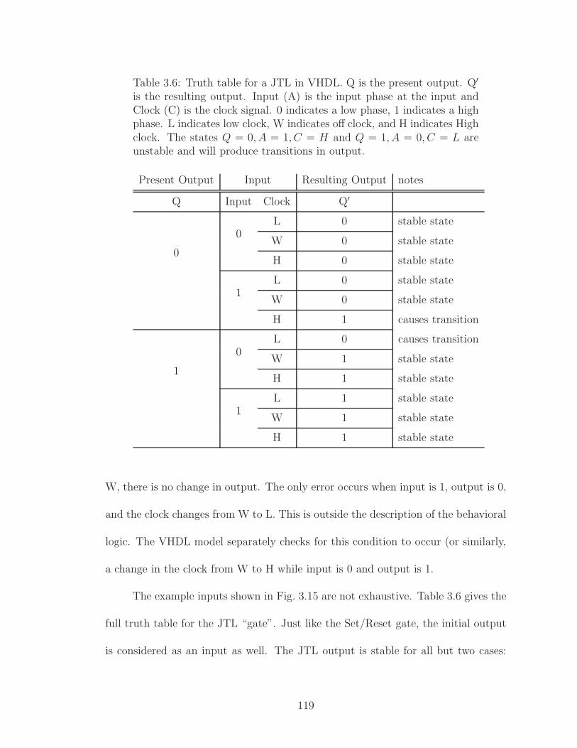
Table 3.6: Truth table for a JTL in VHDL. Q is the present output. Q′
is the resulting output. Input (A) is the input phase at the input andClock (C) is the clock signal. 0 indicates a low phase, 1 indicates a highphase. L indicates low clock, W indicates off clock, and H indicates Highclock. The states Q = 0, A = 1, C = H and Q = 1, A = 0, C = L areunstable and will produce transitions in output.
Present Output Input Resulting Output notes
Q Input Clock Q′
0
0L 0 stable state
W 0 stable state
H 0 stable state
1L 0 stable state
W 0 stable state
H 1 causes transition
1
0L 0 causes transition
W 1 stable state
H 1 stable state
1L 1 stable state
W 1 stable state
H 1 stable state
W, there is no change in output. The only error occurs when input is 1, output is 0,
and the clock changes from W to L. This is outside the description of the behavioral
logic. The VHDL model separately checks for this condition to occur (or similarly,
a change in the clock from W to H while input is 0 and output is 1.
The example inputs shown in Fig. 3.15 are not exhaustive. Table 3.6 gives the
full truth table for the JTL “gate”. Just like the Set/Reset gate, the initial output
is considered as an input as well. The JTL output is stable for all but two cases:
119

when Q = 0, A = 1, C = H ; or Q = 1, A = 0, C = L. While the clock is low, only
the condition Q = 0, A = 1, C = H will change the output to Q = 1. Once this has
occurred, only the condition Q = 1, A = 0, C = L will change the output back. Not
captured in the table is the error detection. I wrote a separate code in the VHDL
model to check for timing violation conditions, which occur when Q = 0, A = 1, C =
W → Q = 0, A = 1, C = L or Q = 1, A = 0, C = W → Q = 1, A = 0, C = H .
Finally I note that the figures here show the transitions occurring instantly. In the
full VHDL model, these transitions occur only after a delay given by (3.13) and
using the αi parameters discussed in Section 3.3.
3.4.4 Summary of RQL Gates in VHDL
RQL gates with input phases behave very similar to CMOS gates with voltage
inputs, as can be seen from Fig. 3.13. This allows them to be used in a similar
fashion and their behavior can be analyzed using existing software design tools
intended for CMOS. However, RQL gates are still subject to certain constraints and
the timing behavior is much different from CMOS. Nevertheless, this behavior can
also be captured in VHDL as shown in this Chapter. The AnotB gate in particular
has certain timing requirements due to the detailed behavior of the gate. It is the
only gate that generates logic errors. Finally, JTL units follow combinational logic
rules as well, with the caveat that the clock signal carries three values which do not
correspond to any particular physical quantity. The JTL is the only “gate” which
generates timing errors.
120

Chapter 4
Power Network Design
4.1 Introduction
In this Chapter, I discuss the design of the network I developed for powering
my RQL circuits. In RQL circuits the power splitter must accomplish several tasks.
First, the splitter must step down the impedance from 50Ω at the pads to 32Ω, the
impedance of the clocklines coupled to transformers within the circuit. Second, it
must not only split the power evenly, but but also recombine the power in the clock
lines to be taken off chip. Third, although it must function over a broad frequency
range, the amount of space it uses on the chip needs to remain small. Fourth, in order
for an RQL circuit to work properly, the distribution of currents between splitters
and combiners must remain within 10% of nominal values within the frequency
range. Finally, the splitter must also maintain these properties when the electrical
length of individual lines between the splitter and combiner are changed by loading
or fabrication.
I first describe a general design for an eight-way Wilkinson power splitter and
discuss three possible responses: geometric, equal ripple, and maximum flat. I then
describe the design of two power splitters that I used for testing RQL circuits. I next
compare results from testing both designs. Finally, I describe a second experiment
using a maximum flat Wilkinson power splitter to power an RQL circuit containing
121

(b)
RN R1RN−1
λ/4
λ/4
Z0
Z0
Z0
√2Z0
√2Z0
R = 2Z0
(a)
Port 1 Port 3
Port 2
Zout
Zout
ZN ZN−1 Z1
Zin
Figure 4.1: Wilkinson Power Splitter. (a) The traditional Wilkinsonpower splitter: one stage with equal impedances at all ports and quarter-wavelength transmission lines. For the design frequency, evenly splitspower without losses between output ports (on right) while completelyisolating the output ports from each other. (b) The general Wilkinsonpower splitter with N stages, 2N transmission lines, and N resistors.Higher bandwidth than one-stage Wilkinson power splitter. Note alsothat input and output impedances need not be equal and we allow anyelectrical length ρ so long as all transmission lines are equal in length.
shift registers.
Figure 4.1 shows the general layout of a Wilkinson power splitter using quarter-
wave length transmission lines and resistors. Figure 4.1(a) shows the most basic
Wilkinson power splitter design with equal impedances on input on left and output
on right. The quarter-wave segment is central to the operation of the power splitter.
For transmission lines of length l the impedance of the line is
Zin(l) = Z0ZL + iZ0 tan βl
Z0 + iZL tan βl, (4.1)
where Z0 is the characteristic impedance of the transmission line, ZL is the load
impedance, and β = 2π/λ is the wavenumber. For quarter-wave segments, this
gives Zin = Z20/ZL, which for ZL = Z0, Zin =
√2Z0. Using this value of the
impedance for the quarter-wave segments, the impedance R seen at the input can
be calculated as the combination of one quarter wave segment in parallel with the
122

resistor and other quarter-wave segment in series, as follows:
1
R=
1
Z0
[1√2+
1
2 +√2
]
=1
Z0
(2 +√
(2)) +√2√
2(2 +√2)
=1
Z0
2 + 2√2
2√2 + 2
=1
Z0
. (4.2)
This gives the effective impedance of the power splitter as Z0, a perfect impedance
match.
Figure 4.1(b) shows a generic layout for a 2-way Wilkinson power splitter with
impedance Zin on the input and impedance Zout on the output, with N stages.
Note that the numbering of resistors and quarter-wave transmission lines starts at
the output. A more thorough description of the Wilkinson power splitter can be
found in many textbooks on electrical engineering, such as [39].
4.2 Circuit Design
I designed a Wilkinson power network in two steps. As I discuss below, I first
minimized the input port reflections in “even” mode and I then maximized the out-
put port isolation in the “odd” mode. Both steps are important for power networks
in digital circuits since reflection at the input port of the power combiner causes
standing waves in the power lines and the corresponding nonuniform distribution
of the current produces potential spikes at the anti-nodes. Odd mode analysis ap-
plies to the situation where the clock lines have different electrical length due to the
different topology of the lines or different load by the gates.
To proceed, I considered a generic Wilkinson power splitter design (see Fig.
4.2). The configuration of a Wilkinson power splitter is specified by giving the num-
123

ber of power splitter segments1 in successive sections. I used a one, two, two, and one
or 1221 configuration. In general, a splitter configuration with M segments is desig-
nated by a0a1 . . . aM. The total number of quarter-wavelength stages is∑M
m=0 2mam
and the number of resistors is∑M
m=1 2m−1am. These are important design metrics
for system integration. These configuration only describe the layout of the power
splitter, not the values of the impedances Zm or resistances Rm. In the next sec-
tion, I introduce three different methodologies for determining the impedances of
the stages.
4.2.1 The Even Mode
Figure 4.3 shows the decomposition of a generic Wilkinson power spitter into
the “even” and “odd” mode. The full response of the circuit to any input at any port
can be found by superposition of the circuits shown in Fig. 4.3(b,c) [39]. In the even
mode, two equal voltages +V are applied to the output ports. Because the potential
across each resistor connecting the upper and lower segments (see Fig. 4.3(a)) is zero
due to symmetry, they can be removed. The resulting circuit is shown in Fig. 4.3(b)
and has the layout of a generic quarter-wave impedance matching filter. Because
the two halves of the circuit behave identically, they are symmetric or even. This
is the primary mode of operation of the power splitter I designed; the odd mode
shown in Fig. 4.3(c) will be of interest later.
In the even mode the Wilkinson behaves like an impedance matching filter
1A note on terminology: In microwave engineering, the term “stage” is common for the quarter-wavelength transmission lines in a WPS. As such, we need a different word to describe groups ofthese stages into hierarchical units. As both “stage” and “segment” are similar in both sound andmeaning, I wish to explicitly note the difference.
124
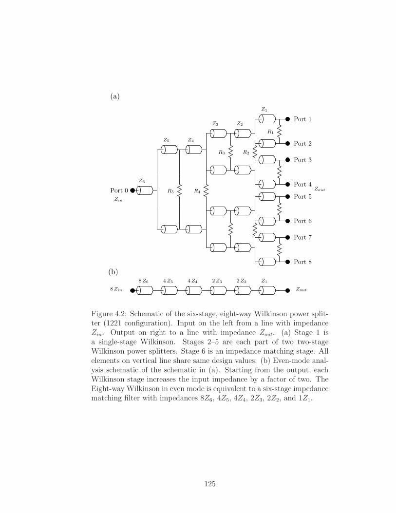
(a)
Z12Z22Z34Z44Z58Z6
Zout8Zin
Zout
Zin
Port 0
(b)
Z1
Z4Z5
Z6
Z3 Z2
Port 2
Port 3
Port 1
Port 4
Port 5
Port 6
Port 7
Port 8
R5 R4
R3
R1
R2
Figure 4.2: Schematic of the six-stage, eight-way Wilkinson power split-ter (1221 configuration). Input on the left from a line with impedanceZin. Output on right to a line with impedance Zout. (a) Stage 1 isa single-stage Wilkinson. Stages 2–5 are each part of two two-stageWilkinson power splitters. Stage 6 is an impedance matching stage. Allelements on vertical line share same design values. (b) Even-mode anal-ysis schematic of the schematic in (a). Starting from the output, eachWilkinson stage increases the input impedance by a factor of two. TheEight-way Wilkinson in even mode is equivalent to a six-stage impedancematching filter with impedances 8Z6, 4Z5, 4Z4, 2Z3, 2Z2, and 1Z1.
125
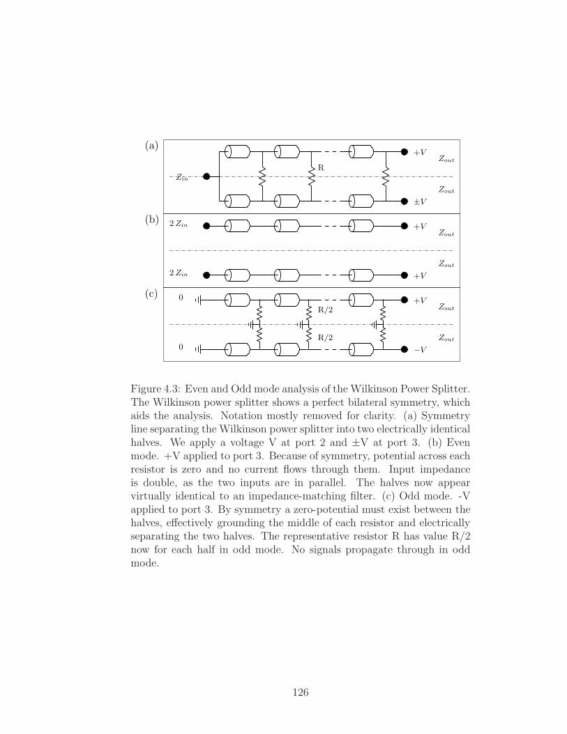
+V
+V
2Zin
2Zin
+V
Zin
±V
Zout
Zout
Zout
Zout
Zout
Zout
R
R/2
R/2
+V
−V
0
0
(c)
(b)
(a)
Figure 4.3: Even and Odd mode analysis of the Wilkinson Power Splitter.The Wilkinson power splitter shows a perfect bilateral symmetry, whichaids the analysis. Notation mostly removed for clarity. (a) Symmetryline separating the Wilkinson power splitter into two electrically identicalhalves. We apply a voltage V at port 2 and ±V at port 3. (b) Evenmode. +V applied to port 3. Because of symmetry, potential across eachresistor is zero and no current flows through them. Input impedanceis double, as the two inputs are in parallel. The halves now appearvirtually identical to an impedance-matching filter. (c) Odd mode. -Vapplied to port 3. By symmetry a zero-potential must exist between thehalves, effectively grounding the middle of each resistor and electricallyseparating the two halves. The representative resistor R has value R/2now for each half in odd mode. No signals propagate through in oddmode.
126

between impedances Zin and Zout. The Wilkinson power splitter is normally ana-
lyzed with equal impedances on both input and output. However, the even- and
odd-mode analysis can be generalized to the case of unequal impedances [39]. The
response of the equivalent impedance matching filter is determined by the choice of
impedances in each stage of the Wilkinson power splitter.
I consider three responses. First, the geometric response is of the form Γ(ρ) ∼
cos(N ρ) + cos((N − 2)ρ) + . . . and has a constant ratio of impedances, making it
easy to design in physical layout. Second, the maximum flat response has the form
Γ(ρ) ∼ (1−e−i ρ)N and fulfills the condition dnΓ/dρn(π/2) = 0 for n = 0, 1, . . . , N−1.
Third, the equal ripple response has the form Γ(ρ) ∼ Tn(cos ρ) where Tn is the
Chebyshev polynomial of the first kind. This gives the broadest bandwidth for a
given maximum reflection coefficient within the bandwidth. The detailed derivation
of filter impedances for the different cases can be found in Appendix C (page 263).
I find [39] for
the geometric response: Zn+1 = ZnN+1
√
2MZin
Zout, (4.3)
for maximum flat response: Zn+1 = Zn × exp(2−NKNn ln(2M
Zin
Zout)), (4.4)
where binomial coefficient KNn =
N !
(N − n)!n!,
and the equal ripple response: Zn+1 = Zn1 + γn1− γn
, (4.5)
where N =∑am is the total depth of the Wilkinson power splitter and γj is propor-
tional to the jth expansion coefficient of the Chebyshev polynomial (see Appendix
B).
ForN = 6 I find the impedance values shown in Table 4.1. Figure 4.4 shows the
127

Table 4.1: Impedance values for the Wilkinson splitter stages for differentconfigurations with N = 6 stages. All values are in Ohms. Values givenin order matching Fig. 4.2. Final design values correspond to Fig. 4.10and are given here for comparison. Fractional bandwidth given for -13dB. Values for final design are constrained by fabrication limitations,unlike for the three other responses.
Z6 Z5 Z4 Z3 Z2 Z1 Bandwidth
Maximum Flat 30.88 50.98 31.31 32.70 20.09 33.06 0.9Equal Ripple 28.19 42.88 28.70 36.47 24.41 37.14 1.2Geometric 23.78 35.33 26.25 39.01 28.98 43.07 0Final Design 47.94 37.24 20.72 19.36 21.44 33.36 0.73
even mode reflection parameters2 for these three configurations as well as the final
design which I used. The geometric response has the largest input mismatch and this
gives the highest reflection at the design frequency and across the bandwidth. The
equal ripple response has better matching and will have lower overall reflections and
a higher bandwidth. The maximum flat response has a smaller bandwidth than the
equal ripple response, but has the lowest overall reflection. At the target frequency
the variation is lowest for the maximum flat response. I discuss my final design in
Section 4.2.5.
The 1221 Wilkinson is not the only configuration for a power splitter. I com-
pare two other configurations, the 4440 configuration and 2220 configuration power
splitter. Figure 4.5 shows the 4440 Wilkinson splitter. (Resistors have been omitted
for clarity.) This kind of design lends itself well to the geometric response, as each
segment has identical impedances in each of the quarter-wave stages. Figure 4.6
shows a similar configuration with only two stages per segment.
2Unless noted otherwise, all S-parameters are given as Sij = 10 log10(Vi/Vj).
128

0
0.1
0.2
0.3
0.4
S11
[linear]
-40
-30
-20
-10
0 0.5 1 1.5 2
Frequency [f/fc]
[dB]
Maximum FlatEqual Ripple
Geometric
Figure 4.4: Wilkinson 1221 Simulated Reflection Parameters for max-imum flat design (red solid), equal ripple design (green dotted), andgeometric design (blue dashed) are plotted as a function of normalizedfrequency in linear and log space. Circuit shown in Fig. 4.2 and circuitparameters correspond to values given in Tables 4.1 and 4.2. Line drawnin at -13 dB (5%) is for reference. Geometric design has high reflectionsover entire design range. Equal ripple has less than -13 dB reflectionover the broadest frequency range (by design), as shown by bottom ar-row. Maximum flat response has smaller range (shown by top arrow)for which reflection is below -13 dB but has the smallest variation ofreflections within the design range.
Figure 4.7 shows the even mode reflection parameters for the splitter design
shown in Fig. 4.5. (Compare with Fig. 4.4.) Notice that the six-stage geometric
series response has high reflection parameters. The six-stage device is similar to
the 12 stage design, though each of the branches with four quarter-wave segments
becomes a branch with two quarter-wave segments, turning it into a 2220 configu-
ration splitter. Comparing the 12-stage geometric series response and the six-stage
129

Z4 Z3 Z2 Z1
Z4 Z3 Z2 Z1
Z4 Z3 Z2 Z1
Figure 4.5: Circuit schematic for Wilkinson 4440 configuration for initialprototype power splitter using a geometric response. Resistors not usedin this design; testing was only done in even mode. Designed for inputand output impedance of 32 Ω. Ratio of impedances for each trans-mission line stage to the next was 2−1/4, such that Z1/
12Z4 = Z4/Z3.
(a)
2Z12Z24Z34Z48Z58Z6
Zout8Zin
(b)
R4 R3
R2 R1
Zout
Port 2
Port 3
Port 1
Port 4
Port 5
Port 6
Port 7
Port 8
Z3Z4
Z5
Z2 Z1
Z6
Port 0
Zin
Figure 4.6: Circuit schematic for WPS2220. Similar to the 4440 design.
maximum flat response, the reflection parameters are similar even though the latter
has half the number of stages.
130

-30
-25
-20
-15
-10
-5
0
0 5 10 15 20
S12[dB]
f [GHz]
fc = 10GHz
Geometric Series
Max Flat Response
12 Stage
6 Stage
Figure 4.7: Geometric versus max flat power splitter reflections. Simu-lated reflection parameters of 1:8 Wilkinson power splitter in even modeusing actual impedance values. The maximum flat response for a 6-stagedeep splitter (red curve, 2220 configuration) is compared to the geomet-ric response for 6 and 12 (4440 configuration) stages (dotted and solidgreen curves, respectively).
4.2.2 The Odd Mode
The second half of the analysis of a Wilkinson power splitter involves applying
a voltage +V to one output port and -V to the other output port, as shown in Fig.
4.3(c). In this case, the circuit has a zero-potential between the top and bottom
halves with, making the two halves appear opposite or odd to each other. Proper
odd mode analysis [39] depends on specific impedance values. We can maintain a
mirror symmetry in the odd mode by treating each segment as an individual power
splitter with ±V at each input.
131

Table 4.2: Resistance values in Wilkinson power splitter for differentresponses. Values in Ohms. Resistors R2 and R4 tend to have verysmall values compared to the rest of the resistors. Final design valuesgiven for reference and correspond to Fig. 4.10, which omits resistors R4
and R2. Final design is for a 3111 configuration, all others are for a 1221configuration.
R5 R4 R3 R2 R1
Maximum Flat 49.29 2.05 31.62 2.08 64Equal Ripple 44.43 2.06 37.39 2.07 64Geometric 39.77 2.06 43.90 2.05 64Final Design 23.56 n/a 20.62 n/a 58.62
For N = 1 the problem is trivial; for N = 2 we follow the method of Cohn3,
which for N = 2 and a fractional bandwidth of 1 gives [40]
R2 =2Z1Z2
√
(Z1 + Z2)Z2
, (4.6a)
R1 =2R2(Z1 + Z2)
R2(Z1 + Z2)− 2Z2, (4.6b)
where R2 and R1 are the resistor values of the resistors in Fig. 4.1(b) and Z2 and
Z1 are the impedances of the quarter-wave transmission lines shown in Fig. 4.1(b).
I can apply (4.6a) and (4.6b) to the results calculated from (4.3), (4.4), and (4.5)
for the circuit shown in Fig. 4.2. The results are shown in Table 4.2.
The odd mode analysis normally completes the design of a power splitter. RQL
circuits place additional requirements on the design. So far I have only considered
a generic 1221 power splitter. I will now also consider several alternative configura-
tions, including a 4440, 2220, and 3111 configuration Wilkinson power splitter.
3Cohn’s original result is R2 = 2Z1Z2/√
(Z1 + Z2)(Z2 − Z1 cot2 ρ3). In Cohn’s method [40]
ρ3 is the fractional bandwidth in units of 2π. For better comparison I simplify the equations fora fractional bandwidth of 1, for which cotρ3 = 0. Fine tuning of the circuit occurs later in thedesign process and this simplification does not impact final results.
132
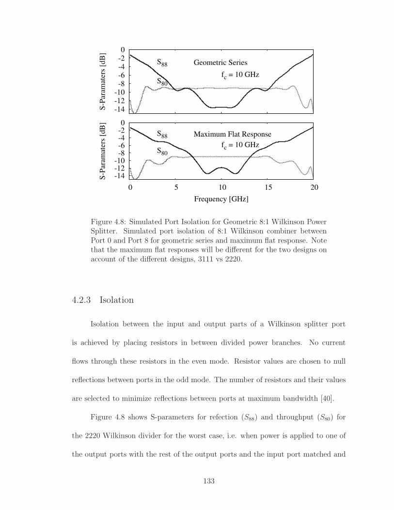
Figure 4.8: Simulated Port Isolation for Geometric 8:1 Wilkinson PowerSplitter. Simulated port isolation of 8:1 Wilkinson combiner betweenPort 0 and Port 8 for geometric series and maximum flat response. Notethat the maximum flat responses will be different for the two designs onaccount of the different designs, 3111 vs 2220.
4.2.3 Isolation
Isolation between the input and output parts of a Wilkinson splitter port
is achieved by placing resistors in between divided power branches. No current
flows through these resistors in the even mode. Resistor values are chosen to null
reflections between ports in the odd mode. The number of resistors and their values
are selected to minimize reflections between ports at maximum bandwidth [40].
Figure 4.8 shows S-parameters for refection (S88) and throughput (S80) for
the 2220 Wilkinson divider for the worst case, i.e. when power is applied to one of
the output ports with the rest of the output ports and the input port matched and
133

Zout
8
7
6
5
4
3
2
1
0 WPS
ZoutZin
Figure 4.9: Isolation parameter measurement. Power is applied to port8 of the Wilkinson power splitter while all other ports are terminated inmatched loads.
terminated (see Fig. 4.9). One can see that the reflection S88 from port 8, where
power is applied, is similar for both responses. Figure 4.8 shows the S-parameters
for a geometric divider similar to that shown in Fig. 4.5 but with only two quarter-
wave segments per stage. The impedance values of this circuit were chosen to give
a geometric series response and a maximum flat response, using actual impedance
values possible in fabrication instead of the ideal calculated values. The choice of
even mode response has little effect on the isolation behavior of the splitter.
As for the even mode analysis, it is worthwhile to consider a new design of the
Wilkinson power splitter. Figure 4.10 shows a schematic of the 3111 configuration
Wilkinson power splitter. This design has fewer resistors and quarter-wave stages
than similar 2220 or 1221 configurations.
Figure 4.11 shows the S-parameters of the 3111 divider shown in Fig. 4.10(a),
using actual impedance values. The circuits were simulated using AC analysis in
the WRspice simulator [41] for the central frequency of 10 GHz, chosen as a design
134

(a)
Z1
8Zin Zout
8Z5 8Z4 4Z3 2Z28Z6
Zout
Zin
Port 0
(b)
Port 2
Port 3
Port 1
Port 4
Port 5
Port 6
Port 7
Port 8
Z1
Z2
Z3
Z4Z5Z6
R1
R2
R3
Figure 4.10: Circuit schematic for N23PS. (a) Schematic of final designfor N23PS, a six-stage, eight-way Wilkinson power splitter. (3111 con-figuration.) Similar to Fig. 4.2. Input line on the left has impedanceZin. Output line on right has impedance Zout. Stages 1 – 3 are single-stage Wilkinsons. Stages 4 – 6 are impedance matching stages. Allelements on vertical line share same design values. Note that resistor R3
in this schematic is equivalent to R4 in Fig. 4.2. Resistors R3 and R5
from Fig. 4.2 have been eliminated in the final design. (b) Even-modeanalysis schematic of the schematic in (a). Starting from the output,each Wilkinson stage increases the input impedance by a factor of two.The eight-way Wilkinson in even mode is equivalent to a quarter-wavetransformer with segment impedances 8Z6, 8Z5, 8Z4, 4Z3, 2Z2, and 1Z1.
135

-50
-45
-40
-35
-30
-25
-20
0 5 10 15 20
Reflection
Coeffi
cient[dB]
Frequency [GHz]
S08
S78
S58
S18
Figure 4.11: Wilkinson 3111 Simulated S-Parameters. Simulated S-Parameters of the Wilkinson 3111 maximum flat response power splitterwhich has a design frequency of 7.5 GHz. All S-Parameters are given as10 log(V/V0). S80 (red) is the ratio of the voltage at the “input” dividedby the voltage applied to output port 8. S88 (light blue) is reflectionoff the output port where the voltage is applied at the output port. S87
(green) is throughput to adjacent port. S85 (dark blue) and S81 (purple)represent ports two and three branches away on the Wilkinson, respec-tively. Within the design frequency range the throughput to Port 0 isabout -5 dB while reflection remains below -15 dB. Throughput to otherports remains under -10 dB.
136

compromise between available real estate and cryoprobe limitations. The design
rules limit the widths of microstrips to certain values, and thus limits the impedances
to certain values.
This design was optimized for a 1:8 Wilkinson transformer with a minimum
required depth N = 6 of λ/4 segments. Impedances of the λ/4 segments were
calculated by analogy with a quarter-wave transformer of the same depth with all
branches taken in parallel, using (4.3) or (4.4) as appropriate. In the geometric
series response, the ratio between two adjacent sections was held constant at 1.34.
Note that in the geometric series response design, the impedances repeat at each
stage, and this makes the design scalable to an arbitrary number of power divisions.
On the contrary, parameters in the maximum flat response have to be recalculated
for each particular case, as in (4.4) above.
The geometric series and maximum flat response designs involve opposite
trade-offs in reflection and bandwidth. As can be seen from S-parameters shown in
Fig. 4.7 the geometric series needs double the number of stages that the maximum
flat response design required to achieve a comparably small level of reflections. In
this case, the reflection S88 at the design frequency is less than -30 dB. The geo-
metric response design with N = 12 shows similar behavior to the maximum flat
response design with N = 6.
137

l = 90 ps
WilkinsonPow
erSplitter
Transm
ission
Lines
6×
WilkinsonPow
erSplitter
Transmission Line 1
Transmission Line 8
Transmission Line 3
Transmission Line 2
Variable Length
Record Currents Here
l = 90 ps
Figure 4.12: Block diagram for measuring standing currents. TwoWilkinson power splitters are connected through eight microwave trans-mission lines, each with a nominal length of l = 90 ps. The bottom sixtransmission lines connect the two power splitters. The second trans-mission line has a variable length l. The top transmission line is simu-lated as eleven shorter transmission lines in series, each with a length ofl = 8.18 ps. In simulation, the currents between the short transmissionlines can be recorded. These currents are plotted in Figs. 4.13 and 4.14.
4.2.4 Current Distribution
The main consideration in choosing one power splitter design over another
is the requirement for current uniformity in the clock power lines. I analyzed the
current uniformity by embedding relatively long τ = 90 ps (l = 9 mm) clock power
lines between two dividers (one of which was used as a combiner) and monitoring
the current profile at 10 equally spaced points of 9 ps apart. (See Fig. 4.12.)
Figure 4.12 shows a block diagram of the setup used to simulate standing
138

Figure 4.13: Simulated standing wave currents at ten locations insideclock lines between power splitters in the 4440 configuration, as shownin Fig. 4.16. Nominal and 10% of bias current are indicated by straightlines. Graphs offset for clarity. Imbalance refers to extra electrical lengthof only one line.
waves in the transmission lines. Two Wilkinson power splitters are connected by
eight transmission lines in total. Six are regular transmission lines with electrical
length l = 90 ps on ports 3–8. Port 2 is connected to a transmission line with length
l, which I vary in simulation to induce odd mode behavior in the Wilkinson power
splitters. Port 1 is connected to a series of 11 shorter transmission lines with length
l = 8.18 ps. Though this transmission line is of the same overall length, in the
simulation I can record the currents at the nodes between shorter transmission line
segments. (See Appendix C, Section C.3 on page 268 for the netlist used to generate
this data.)
139

Figure 4.13 shows the results from standing wave analysis for the case when
the electrical length of one power line is either 0 ps or 40 ps longer than the others.
In this simulation, I used the 2220 splitter configuration, as shown in Fig. 4.6. For
comparison, Fig. 4.14 shows the results from the standing wave analysis for the
case when the electrical length of one power line is either balanced or 10% longer
than the others for the 3111 design shown in Fig. 4.10 (only for the maximum flat
response). The former case corresponds to 44% imbalance in electrical length, which
far exceeds the expected worst case in a practical circuit.
As described in Chapter 2 (pg. 75) the delay is less than 2 ps for 106 junctions.
In that experiment, the coupling between clock lines and junctions was greater by a
factor of three than in regular RQL circuits. It would take 107 Josephson junctions
to accumulate this amount of phase delay due to dynamic switching [27]. Junction
switching therefore does not contribute to an imbalance in the power splitters. In
Nb microstrips with a propagation speed of about 100 µm/ps, it will take 4 mm to
accumulate 40 ps of delay. This is a large distance compared to the scale of circuit
elements, and therefore small variations in the clock length through a chip will also
not contribute greatly to imbalances in the power splitters.
Figure 4.13 shows that the expected distribution of the bias current is signif-
icantly different between the geometric series and maximum flat response for the
2220 splitter. The maximum flat response is designed to have minimum variation
within the bandwidth, and this property carries over to the bias current distribu-
tions. Figure 4.14 shows that the distribution of the bias current is significantly
different between the 2220 layout (see Fig. 4.6) and the 3111 layout (see Fig. 4.10).
140

The geometric series with 6 stages does not satisfy requirements of ± 10% variation
in bias current (see Fig. 4.13). In contrast, the maximum flat response for the 3111
design gives an octave of bandwidth (5-15 GHz) with no more than ± 10% vari-
ance in bias current (see Fig. 4.14). Between 8.5-11.1 GHz the 3111 design gives
± 1% variation. This indicates that maximum flat response performs much better
for our figure of merit of current uniformity. The 3111 design does even better be-
tween about 7–13.5 GHz with ± 1% variation. The 3111 design also saves space by
matching between 50Ω and 32Ω, which the 2220 design does not.
4.2.5 Final Design
To test the capabilities of Wilkinson power splitters I had two designs fabri-
cated, which I will denote as Monrovia 20 Power Splitter (M20PS) and Norwalk 23
Power Splitter (N23PS). The first design, M20PS, is a 4440 configuration Wilkinson
and has a geometric response and no isolation resistors (see Fig. 4.5). I used this de-
sign to test the even mode response of a power network. The second design, N23PS,
seen in Fig. 4.10, is a 3111 Wilkinson and has an optimized maximum flat response.
I chose the parameters for this design it using (4.4), (4.6a) and (4.6b). In a second
iteration of the design of N23PS, the impedances and resistors were simulated and
fine tuned to produce better standing wave ratios. In addition to good responses
in the even and odd modes, I also checked the behavior of the currents that flow
between splitters and combiners.
141

0
0.5
1
1.5
2
0 5 10 15 200
0.5
1
1.5
2
Nom
inal
Current[naturalunits]
Nom
inal
Current[naturalunits]
Frequency [GHz]
Figure 4.14: Standing Waves in Wilkinson 3111 Power Network. Simu-lated current amplitudes at ten points along the transmission line con-necting Wilkinson 3111 power splitters in Fig. 4.10 as a function of fre-quency. Top graph (green) shows results with eight transmission lines ofequal length between Wilkinsons with f = 10GHz designed center fre-quency. Bottom graph (red) shows same currents along a regular lengthof transmission line when another line has a 10% longer electrical length.±10% lines shown for reference. With the maximum flat design and nolength imbalance the currents stay within ±10% between about 5 GHzand 15 GHz, with less than 1% variation between about 7 GHz and 13GHz. With the 10% length imbalance, the operational range with lessthat 10% variation in bias current is between about 6 GHz and 14 GHz,with substantial variation throughout. Graphs offset for clarity.
142

calibrated reference planes
c1 c1*
a0
c0 c0*
dc0 dc0*
q0Circuit
4.2 K
a0*
c1 c1*
a0
c0 c0*
dc0 dc0*
q0Circuit
4.2 K
a0*
or
Calibrated Lines
Network Analyzer
Calibrated Lines
Network Analyzer
Figure 4.15: Experimental setup for measurement of S-parameters. S-parameter measurements were performed only on inactive circuits andno other equipment was attached. The network analyzer was connectedto the clock input and output of the probe. Using either a standards kitor a standards chip, the network analyzer could be calibrated to the topof the probe or to the pads on the chip.
4.3 Standalone Test
To test the above simulation results, I designed and had fabricated two Wilkin-
son splitters. The first one, N20PS, is shown in Fig. 4.5(a) and was designed with a
geometric series in the 4440 configuration. The second one, M23PS, is shown in Fig.
4.10 and was designed with the maximum flat response in the 3111 configuration to
measure isolation.
To measure the S-parameters of the M20PS and N23PS circuits, I used the
setup shown in Fig. 4.15. The coaxial cables leading to and from the network an-
143

alyzer were calibrated out of the measurement using a standards kit. Calibration
chips were also available, though because the chip had not been characterized, the
network analyzer used a generic profile for the standards chip. Ultimately, calibrat-
ing to the top of the probe with the calibration kit with a known profile yielded
better results.
4.3.1 Experimental Setup
Figure 4.16 shows a microphotograph of the geometric response 1:8 Wilkinson
divider/combiner M20PS test circuit. Due to limited space on the chip only the
12-step geometric series response even mode circuit was tested. The circuit was
optimized for a center frequency of 17 GHz and 10 GHz bandwidth. The impedance
values were adjusted to accommodate the available discrete values of the width of
signal wire due to the 0.5µm lithography step (see Table 4.1). The total occupied
area of the circuit is 630µm(0.08λ)× 1550µm(0.2λ) with approximate dimensions
of one segment of 400µm (0.05λ)× 320µm (0.04λ). The dimensions of the circuit
compare favorably with previously published lumped-element and distributed de-
signs [42, 43]. The clock signal enters from the left at port 1, is split eight ways, and
then combined and taken off chip on the right at port 2 (see Fig. 4.16). Figure 4.16
shows a test circuit schematic with a 18.5 dB resistive tap added to monitor current.
The tap is included in the bottom power line at an electrical distance of approxi-
mately 0.13λ from the power splitter output port. To balance the circuit, identical
taps are added to other lines and resistively terminated on chip (not shown). The
144

32 32
4.2 K
t = 90 ps
Port 1
27042
32321.6 1.6 t=45 pst=45 ps
Port 3
50 50
50
Port 2
(b)
(a)
Figure 4.16: M20PS even mode test. (a) Microphotograph of M20PScircuit showing input, output, and 20 dB tap array (left). Fabricated byHypres using the 4.5 kA/cm2 process. (b) Circuit schematic of M20PScircuit. All ports were impedance matched. The impedance-matchedtap is shown only on one line for clarity. All other lines had a similartap but grounded directly on chip instead of going to a pad.
145

circuit has three contact pads to monitor power at each port.
Figure 4.17 shows a microphotograph of the chip containing N23PS, the maxi-
mum flat response 3111 Wilkinson divider/combiner test circuit. I used this chip to
test the 6-stage maximum flat response in even and odd mode. The circuit was op-
timized for a center frequency of 7.5 GHz with a 6 GHz bandwidth. The impedance
values were adjusted to accommodate the available discrete values of the width of
signal wire due to the 0.5µm lithography step (see Table 4.1). The physical size of
the power splitter in N23PS is comparable to that of the geometric response Wilkin-
son in M20PS. The size of the N23PS relative to the wavelength of the M23PS is
smaller by a factor of 7.5/17 = 0.44, although this comparison does not take into ac-
count the different fractional bandwidth. This circuit was designed with RQL shift
registers with separate inputs to differentially load the lines and cause an imbalance
in the power network. Unfortunately, design errors on the chip prevented all but
one of the shift registers from being utilized. Nevertheless, I was still able to obtain
S-parameter measurements of both pairs of splitters and combiners on chip.
I tested the Wilkinson divider/combiners using an American Cryoprobe (ge-
ometric response) and a High Precision Devices (HPD) probe (maximum flat re-
sponse) with the microwave test setups shown in Figures 4.16 and 4.17 respectively.
The American Cryoprobe probe is designed for a 3 dB at 10 GHz cutoff frequency
and has pressure contacts. The HPD probe has a 5 dB cutoff at 26 GHz. For both
probes, a calibration of the coaxial lines leading from testing equipment, though
the probe, and to the chip was performed on a separate chip for different combi-
nations of the contact pads to accommodate the spread in electrical parameters
146

Wilkinson Power Splitter
Input
Input Output
Output
ShiftRegisters
Shift
Registers
Wilkinson Power Splitter
5 mm
5mm
Figure 4.17: Microphotograph of Norwalk 23. The N23PS circuit isshown on this chip. The four Wilkinson power splitters (red boxes)are in the four corners of the chip. The bottom two and top two areconnected by eight lines between them. Input and output to each ofthe splitter/combiners is shown. Eight shift registers are in the mid-dle (green boxes). Data input to the shift registers is on the left (notmarked); output is on the right. This chip was used to test the oddmode analysis of a 6-stage maximum flat series response 1:8:1 Wilkinsonpower splitter/combiner.
147
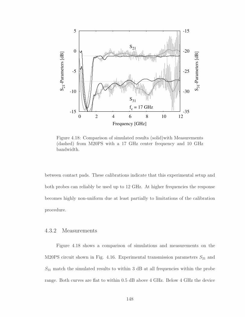
Figure 4.18: Comparison of simulated results (solid)with Measurements(dashed) from M20PS with a 17 GHz center frequency and 10 GHzbandwidth.
between contact pads. These calibrations indicate that this experimental setup and
both probes can reliably be used up to 12 GHz. At higher frequencies the response
becomes highly non-uniform due at least partially to limitations of the calibration
procedure.
4.3.2 Measurements
Figure 4.18 shows a comparison of simulations and measurements on the
M20PS circuit shown in Fig. 4.16. Experimental transmission parameters S21 and
S31 match the simulated results to within 3 dB at all frequencies within the probe
range. Both curves are flat to within 0.5 dB above 4 GHz. Below 4 GHz the device
148

acts like a current divider and not a power divider. Experimental and simulation
results for power at the tap (S31) agree well within 1 dB between 3-7 GHz. Both
curves show an approximately 1.8 GHz periodicity which corresponds to pad-to-pad
resonance (5.5 mm) due to impedance mismatch at the pressure contact. The dips
at 8 GHz and 11 GHz are due to inaccuracy in the probe calibration. From the
results, I can conclude that overall response at the tap in the M20PS circuit is flat,
which indicates no standing waves in the power line.
Figure 4.19 shows Spice simulation results of the 3111 circuit shown in Fig.
4.17 with both 0 ps and 40 ps imbalance in one of the lines connecting the splitter
to the combiner for a center frequency of 7.5 GHz. Outside the bandwidth (about
4.5–10.5 GHz) the simulation with an imbalance plays little role. Within the region
of interest, the 0 ps imbalance has very low reflection below -20 dB. Even with a 40
ps imbalance the reflection is between -10 and -20 dB. Thus, in this range which is
the desired response of the maximum flat design, the reflection is still very flat.
Figure 4.20 shows measurements of the N23PS maximum flat response (3111)
Wilkinson power splitter/combiners with a center frequency of 7.5 GHz. This data
comes from N21CLA, which had an identical design of the power splitter4 as in
N23PS, now was on a different chip. Experimental transmission parameters S12
(purple) and S21 (blue) match simulations shown in Fig. 4.19. The expected fre-
quency range based on simulation is between 4.5 GHz and 10.5 GHz. As can be seen
in Fig. 4.20, the measured bandwidth reaches from about 3.5 GHz to 11 GHz, beyond
which the transmission parameters become considerably smaller. The transmission
4See Chapter 6
149

00.20.40.60.81
0 2 4 6 8 10 12 14-30
-25
-20
-15
-10
-5
0S-Param
eters(linear)
S-Param
eters(dB)
Frequency f (GHz)
∆f/f = 1
Throughput (S12)Reflection (S11)
Throughput (S12) w/ 40 ps imbalanceReflection (S11) w/ 40 ps imbalance
Figure 4.19: Simulated reflection for the N23PS circuit with a configu-ration as shown in Fig. 4.10. Green (dotted) curve shows nominal casewith no imbalance between lines connecting power splitters. Red (solid)curve shows the results on the overall reflection parameter S11 at eitherinput or output port of the whole power network when a 10 ps imbalanceis in one of the eight lines between power splitters. Close to the centerfrequency the reflection (solid green) is less than -25 dB, whereas withthe imbalance the reflection (dashed green) ranges from -20 dB on thelow end to -10 dB lower than 4 GHz or higher than 10 GHz.
150

parameters of the maximum flat response Wilkinson splitter/combiner compares fa-
vorable with the transmission parameters of a simple through line between pads,
shown as the dotted black curve in the Fig. 4.20. The inset shows the transmis-
sion is fairly flat, usually within 1 dB, between 3 GHz and 12 GHz. As with the
4440 design, below 3 GHz the 3111 power divider acts like a current splitter. The
reflection is around -20 dB but reaches closer to -10 dB at some points, notably
one peak close to 6 GHz. The flat nature of the responses indicates only minimal
standing waves. Finally, I noticed that during layout, part of the 8th segment was
inadvertently shortened by 1/20th of a wavelength at 7.5 GHz. The results here thus
contain an imbalance of at least 2 ps on one of the lines.
4.3.3 Power Splitter Test Conclusions
Among the two designs I tested (M20PS and N23PS) the geometric response
was the least desirable because it had the highest reflections within the range of
interest. Figure 4.10 shows the schematic of N23PS. The values of R2 and R4 in
the 1221 design of Fig. 4.2 were uniformly small for all responses. They dissipated
relatively little power compared to R3 andR5 and I have discarded them in the design
of N23PS. This reduces the splitter from a 1221 configuration to a 1111 configuration
with only 15 transmission line stages and seven resistors in total. Adding two stages
to create a 3111 Wilkinson with N = 6 costs little in space, which is why I chose
the 3111 configuration for the design of N23PS. Compare this to the 21 stages and
10 resistors in the 4440 configuration. The extra stages in the 3111 design help step
151

-30
-25
-20
-15
-10
-5
0
0 5 10 15 20
S-param
eters[dB]
f [GHz]
(a)S11S22S21S12
Through S12
-10
-9
-8
-7
-6
-5
-4
-3
-2
2 4 6 8 10 12
S-param
eters[dB]
f [GHz]
(b)S21S12
Figure 4.20: Measured S-parameters on N21CLA Wilkinson power split-ter. (a) Blue and purple curves show throughput S12 and S21. Redand green show reflections S11 and S22. The throughput (S12) from cal-ibration measurements of a standards chip is shown as a gray curve forreference. (b) A detailed view of the throughput up to 12 GHz. Betweenabout 3 GHz and 12 GHz the curve is relatively flat. The noise on S11
was due to a damaged connector on the network analyzer.
152

down the impedance from Zin = 50Ω to Zout = 32Ω. For the N23PS circuit I found
the initial impedance values using (4.4) and used (4.6a) and (4.6b) for the resistor
values. I then simulated the Wilkinson 3111 with the schematic shown in Fig. 4.17.
(The netlist is given in Appendix C.) Using commercial software (Agilent Advanced
Design System 2009) I optimized the impedances and resistors to get the desired
frequency responses.
Figure 4.21 shows the results of this optimization on the isolation and crosstalk
responses in the N23PS circuit. Using only three resistors between ports, the iso-
lation is substantial. Most power is absorbed, with less than -50 dB reaching the
input port and even less reaching any output ports. Figure 4.14 shows the effect
of line imbalances on the distribution of current in transmission lines between the
Wilkinson power splitters. The effect of imbalances on current distributions is small.
When perfectly matched, the transmission lines have almost no variation over 6 GHz
range and are still within 10% of nominal down to about 5 GHz. Even a 40 ps im-
balance still has all currents within the tolerances down to 5 GHz. On chip, this
would amount to a 1 mm or more difference in length on a 10 square millimeter
chip, much more than is expected.
Figure 4.19 shows the overall reflection of the whole power network for the
optimized 3111 design used in N23PS. A 10 ps imbalance changes the reflection
coefficient from -30 dB to about -20 dB. Though this is a jump of 10 dB, the overall
reflection still remains low, no higher than other elements in a testing setup. (See
Appendix C for details on the S-parameters of the probe itself.) The experimental
test of M20PS suffered from pad-to-pad resonances. Figure 4.19 indicates that these
153

Input Reflection
Output Reflection
Isolation
fc = 7.5 GHz
Figure 4.21: S-parameters from ADS for N23PS. Three curves charac-terizing the final design of N23PS calculated from ADS. Input reflectionis S00, the reflections off the input port to the Wilkinson power splitter.Output reflection is S88, the reflection off of signals arriving at one of theoutputs. Isolation is S78, the signal at an adjacent port when a signalarrives at one of the outputs.
small variations may be even smaller in the final design.
The tolerance to imbalances in the clock lines of the N23PS power splitter is
smaller than for the previously studied Wilkinson 1221 configuration power splitter.
However, the design of the N23PS Wilkinson incorporates a 50Ω input impedances,
eliminating the need for a separate high-bandwidth transformer. The maximum flat
response design used for N23PS has a bandwidth appropriate to RQL circuit needs.
Furthermore, it displayed adequate current uniformity. The design is also space
efficient. Looking ahead, I will need four splitters on each chip with more than one
154

clock phase and more than one parallel pipeline. For each chip, efficient size is a
design necessity.
4.4 Test with RQL Circuits
After completing the test described in Section 4.3, I still needed to test the
Wilkinson power splitter in an RQL circuit. From here forward, the design used was
the maximum flat response Wilkinson power splitter in the 3111 configuration and
fabricated on the N23PS and N20CLA circuits. This design minimizes the effects
of imbalances and achieves a broad frequency operating range.
Despite design and fabrication problems, the chip pictured in Fig. 4.17 still had
one functioning shift register powered by the Wilkinson power splitters. Although
differential loading of the circuit by selectively turning shift registers on and off was
not possible, I was still able to measure the clock power margins on the shift register.
The power margins can be found by noting that the RQL shift register will fail if
at any point along the clock line powering the shift register the current becomes
too high or too low. If too low, the SFQ pulse will fail to propagate. If too high,
the junctions will switch without input and generate a continuous series of pulses.
Both cases can be readily observed using an oscilloscope. In both cases, failure is
defined as the power at which the output becomes probabilistic, the output voltage
sometimes registering as high and sometimes as low for a given pulse.
155
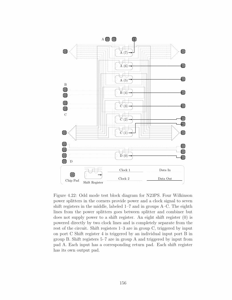
C
B
Shift Register
Clock 1
Clock 2
Data In
Data Out
D
A
Chip Pad
A (7)
A (6)
A (5)
B (4)
C (3)
C (2)
C (1)
D (0)
Figure 4.22: Odd mode test block diagram for N23PS. Four Wilkinsonpower splitters in the corners provide power and a clock signal to sevenshift registers in the middle, labeled 1–7 and in groups A–C. The eighthlines from the power splitters goes between splitter and combiner butdoes not supply power to a shift register. An eight shift register (0) ispowered directly by two clock lines and is completely separate from therest of the circuit. Shift registers 1–3 are in group C, triggered by inputon port C Shift register 4 is triggered by an individual input port B ingroup B. Shift registers 5–7 are in group A and triggered by input frompad A. Each input has a corresponding return pad. Each shift registerhas its own output pad.
156

4.4.1 Power Margin Experiment
Figure 4.22 shows a schematic of the circuit I used to find the power margins in
the N23PS circuit. Eight shift registers are labeled with a unique number (starting
with 0 at the bottom) and a letter corresponding to four pairs of pads A – D. Each
pair of pads is connected in series to a corresponding set of shift registers. Thus,
shift register 0 (SR0) is part of group D, and so on. Each group of shift registers
is triggered by the same input. Four power splitters supply two-phase clock power
to the shift registers in A, B, and C, with an eighth line between the splitter and
combiner which is unloaded by any digital circuits. Group D serves as a control
circuit and has an identical but completely isolated shift register. I used this circuit
to check for malfunctions in either the other shift registers or the power network.
Each shift register outputs to a different output pad. Not shown are two dc bias lines
for D (separate) and A, B, and C (in series). This setup allows certain branches to
be loaded while others are left unloaded to determine the effects of RQL loading on
the power network. The network analyzer can also be used on the power networks,
although not while the RQL circuits are engaged.
The experimental procedure is as follows: First I established the optimal op-
erating point. For a given frequency, the optimal operating point (for flux bias
and input phase) will depend on the phase between clocks, the offset between data
and the clocks, and the clock power. Because of the self-correcting timing of RQL
circuits the data offset has little effect over a broad range of operation. The rela-
tive clock phase between the two clock lines, which should be offset by π/2, is the
157

most sensitive parameter. After I found a general operating point by adjusting the
relative clock phase, clock power, and input phase, I turned the clock power down
until the circuit was barely functional. I then adjusted the clock phases until cor-
rect operation was established. I then turned down the power again, repeating the
process until any significant change of the clock phases resulted in failure. At the
low-power, optimum clock phase point I turned the data phase up and down, noting
failure points, before returning it to the middle of the range. This established the
low power margin. From here, I turned the power up until failure. This established
the high power margin.
One feature of RQL is that the reciprocal pulses need not follow on the same
clock cycle. The Anritsu pattern generator I used is rated only up to 12 GHz for
a non-return-to-zero (NRZ) output, essentially limiting me to 6 GHz data input
speed. However, by “over-clocking” the clock signal by a factor of 3/2 faster than
the return-to-zero (RZ) data rate, the reciprocal pulses can follow one-and-a-half
clock cycles later instead of one-half clock cycles later. For example, a data steam
triggered off of 6 GHz signal will generate a positive SFQ pulse every 166.6 ps. These
pulses can be propagated on an RQL circuit being clocked at 9 GHz. Instead of
following half a clock cycle later (as measured by the ac bias applied to all junctions),
the reciprocal pulse follows one-and-a-half clock cycles later. Although this does not
increase the data speed, it does allow the power splitter to work at higher frequencies
where the power network may have better performance.
158

4.4.2 Data and Analysis
Figure 4.23 shows the results of my power margin measurements on the M20PS
circuit. The input power for high and low margins (adjusted for the attenuators and
other equipment attached to the probe) is shown by the black points. The region of
correct operation is shown as the green shaded area between these data points. On
the top of the figure, the power margin in dB is shown by the black curve. Red and
blue curves are measurements of the S-parameters of the power network5 from input
chip pad to output chip pad. Above 6.5 GHz data rate the clock rate was increased
to 32the data rate, which is marked by the “overclock” region in the Figure.
Examining 4.23, we see that the S-parameters look similar to those measured
previously (compare to Fig. 4.20). I also note that between about 4 GHz and 8.5
GHz the power margins are between 2 dB and 5 dB. The power margins are on
average about 2.4 dB in width, or about ±36%. Above 8.5 GHz the data input rate
is approaching 12 GHz NRZ, the maximum rated for the equipment. At 1.75 GHz,
where the power splitter has a very high local throughput and almost no reflection,
the power required takes a sharp drop, as expected. In the region between 4 GHz
and 8.5 GHz the throughput (S12 and S21) and average power are flat.
Table 4.3 shows the pad-to-pad and splitter-to-combiner lengths for the N23PS
circuit in units of the wavelength at the frequencies of interest. The length of each
quarter-wave segment in the power splitter is approximately 4421µm in length, with
5Note that these measurements are from N23PS. The data shown in Fig. 4.20 is taken fromN21CLA. Because N23PS contained design and fabrication errors I have avoided relying on datafrom this circuit if at all possible. However, here I am comparing the behavior of the power networkto the behavior of the circuit powered by this same power network. A valid comparison can onlybe made by this direct comparison.
159

-30
-25
-20
-15
-10
-5
0
5
0 1 2 3 4 5 6 7 8 9-30
-25
-20
-15
-10
-5
0
5
Pow
er[dBm]
S-Param
eter
[dB]
f [GHz]
Overclock
Power RangePower Margins
S12 & S21S11 & S22
Figure 4.23: Wilkinson-powered RQL circuit measurements of N23PS.Clock amplitude margins (black) overlaid with S-parameters (blue andred) of the on-chip power network. Green region shows operational rangeof SR1 after adjusting input power for losses in the splitter, attenuator,and on-chip power network. Size of the margins is shown above, rangingfrom 0 dBm to almost 5 dBm. S-parameters are overlaid with throughputin red (S12 and S21) and reflection in blue (S11 and S22). Measurementsin both directions are shown in solid and dashed lines. The overclockregion shows where data was taken with the data rate equal to 3/2 theclock speed. Particularly noticeable is the correspondence between thethroughput and the power range over the 3–9 GHz operational region.Frequency is given for the clock speed, not data input speed.
160
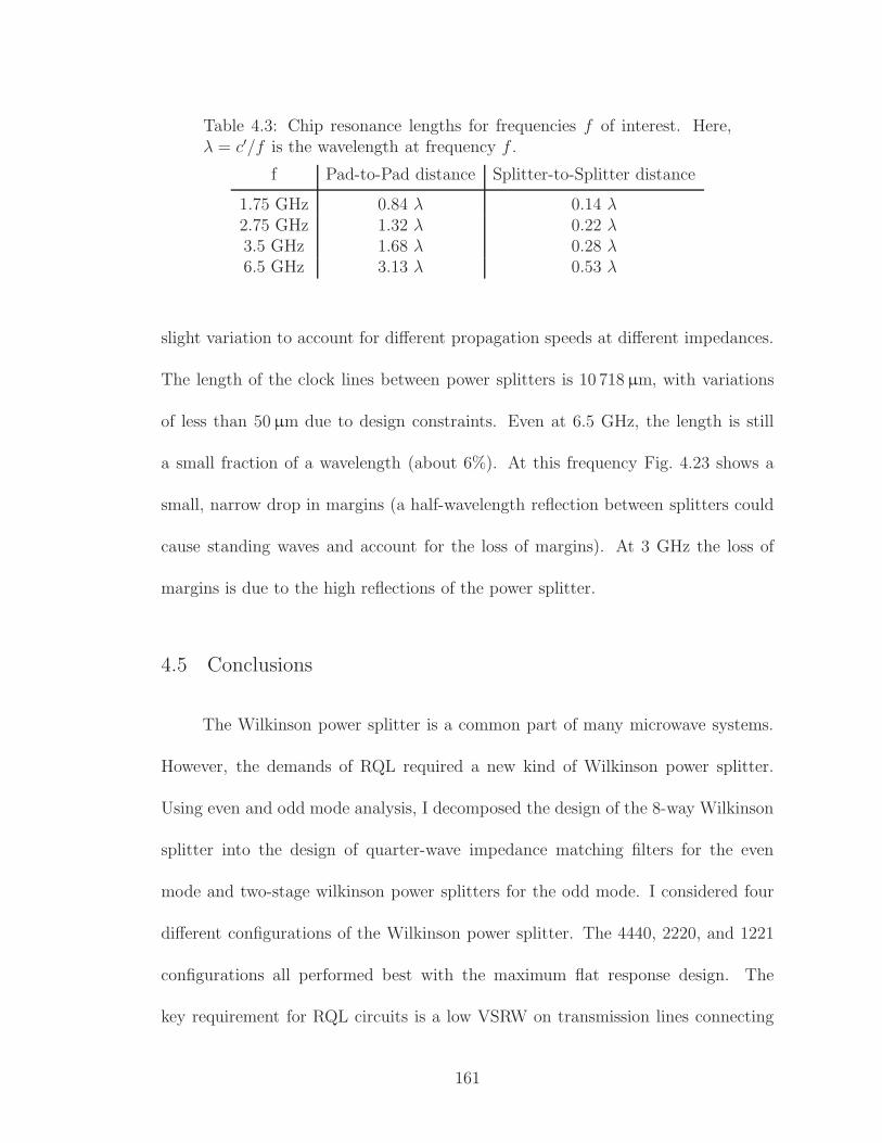
Table 4.3: Chip resonance lengths for frequencies f of interest. Here,λ = c′/f is the wavelength at frequency f .
f Pad-to-Pad distance Splitter-to-Splitter distance
1.75 GHz 0.84 λ 0.14 λ2.75 GHz 1.32 λ 0.22 λ3.5 GHz 1.68 λ 0.28 λ6.5 GHz 3.13 λ 0.53 λ
slight variation to account for different propagation speeds at different impedances.
The length of the clock lines between power splitters is 10 718µm, with variations
of less than 50µm due to design constraints. Even at 6.5 GHz, the length is still
a small fraction of a wavelength (about 6%). At this frequency Fig. 4.23 shows a
small, narrow drop in margins (a half-wavelength reflection between splitters could
cause standing waves and account for the loss of margins). At 3 GHz the loss of
margins is due to the high reflections of the power splitter.
4.5 Conclusions
The Wilkinson power splitter is a common part of many microwave systems.
However, the demands of RQL required a new kind of Wilkinson power splitter.
Using even and odd mode analysis, I decomposed the design of the 8-way Wilkinson
splitter into the design of quarter-wave impedance matching filters for the even
mode and two-stage wilkinson power splitters for the odd mode. I considered four
different configurations of the Wilkinson power splitter. The 4440, 2220, and 1221
configurations all performed best with the maximum flat response design. The
key requirement for RQL circuits is a low VSRW on transmission lines connecting
161

power splitters, for which the maximum flat response is a clear choice. In the final
design of the power splitter, I chose a 3111 configuration with 50Ω input and 32Ω
output. Starting from an initial design using the maximum flat response, I used
ADS software to further increase the performance of the power splitter.
In the second half of this chapter I presented experimental measurements in
Wilkinson power splitters that shown they can be used for power RQL circuits.
In addition to even and odd mode analysis, I used general filter theory to create
three designs. This resulted in the 3111 design shown in Fig. 4.10 with the design
parameters shown in Tables 4.1 and 4.2. My measurement on this design revealed
that the bandwidth was larger than expected and the margins were adequate.
162

Chapter 5
Experimental Verification of RQL Timing Parameters
5.1 Introduction
In Chapters 1 and 2, I described the foundations of Reciprocal Quantum Logic.
In Chapter 3, I described the timing parameters of RQL and corresponding VHDL
models that I used to develop larger circuits. This chapter describes my effort to
verify the timing behavior of junctions predicted by the analytic timing model (eq.
(3.8)) in Chapter 3. With this in mind, I designed and tested three circuits in order
to measure: (1) the timing delay of junctions on a single phase as a function of
input phase, clock frequency, and clock amplitude; (2) operating margins on the
input phase and clock amplitude as a function of frequency; and, (3) operational
margins of the clock amplitude and frequency for a long, deep pipeline shift register.
With these three experiments I was able to test the timing behavior predicted
by equation (3.8), verify the operational boundaries derived from this equation, the
switching time t0, and test the self-correcting influence of the clock boundaries on
input phase delay. These results confirmed the timing behavior of SFQ pulses, and
also showed that RQL circuits can operate over greater input phase ranges than
expected based on my models.
Figure 5.1 shows a microphotograph of the experimental chip. I designed this
chip, designated Norwalk 22 Timing Experiment, or N22TE, and had it fabricated
163

Set
Short Shift
Register
And-output
Race Circuit
Long Shift
Register
Two-output
Race Circuit
5 mm
Standards
5 mm
Figure 5.1: Microphotograph of N22TE, fabricated at Hypres. This chipcontains three experiments on RQL timing. The chip contains one longshift register (red box), two short shift registers (dark blue boxes), twoAnd-output race circuits (green boxes), two Two-output race circuits,and a set of standards (yellow box). Pads on the far left include a set ofstandards with a through-line, 50Ω on-chip termination, an open, anda short. Note that this layout is flipped from the design layout by thefabrication process. The short shift registers were used only to confirmoperation of the chip.
164

at Hypres (see Appendix E for details of the Hypres process). The the circuits
I used for the three experiments can be seen on the chip. I duplicated some of
the circuits to mitigate the chance of fabrication errors disabling a circuit. Three
different circuits were used because no single circuit can test all aspects of the
timing model. In the first circuit I measured the output timing as a function of
input timing by comparing the timing difference between two identical SFQ pulses
in a race condition. These two pulses propagate through two parallel JTL lines with
different lengths, and each line has a separate output. I observed the output of
this two-output race circuit experiment directly on a Tektronix TDS 8000 Digital
Sampling oscilloscope1.
In a second experiment, I alternatively compare two propagating pulses fed to
the AND gate on chip. While this method lost information on the relative timing,
it eliminates the uncertainty introduced by the testing equipment. This and-output
race circuit experiment provided a binary result of correct or incorrect operation as
a function of input time and clock frequency and amplitude, and thus was a good
test of the operational margins.
In the third experiment I tested a long shift register circuit and examined the
behavior of SFQ pulses crossing clock boundaries. In this experiment, I measured
the maximum operating frequency of the long shift register with deep pipelines. The
measured frequencies correspond to the maximum operating frequency of the circuit
with a given pipeline and serve as an experimental measure of the switching time
parameter t0. Also, the timing model predicts a stability limit after which pulses will
1All references to an oscilloscope in this Chapter refer to this model.
165

no longer have self-correcting timing (see pg. 88). I measured the phase boundaries
for correct operation and checked these boundaries against the predictions of the
analytic model.
5.2 Circuits and Simulation for Experiments 1, 2, 3
Figure 5.2 shows block diagrams and a view of the circuits in the Cadence
computer design environment.
5.2.1 Simulation of Experiment 1 — Two-output Race Circuit
In the first experiment, an SFQ pulse generated by a single input splits into two
pulses propagating along separate paths with a different number of junctions (see
Fig. 5.2(a)). The difference in number of junctions between paths was designed to
accumulate enough time delay that could be measured directly on the oscilloscope.
Figure 5.3 shows waveforms of pulse propagation between short and long paths
simulated at 4 GHz. The short track contains 4 JTLs with 8 junctions and the long
path contains 20 JTLs with 40 junctions. The last JTL on both paths is shaded
on the figure. It is an amplification JTL with twice the critical current, required
for the input to the output amplifier. One can see that the total accumulated
delay is around 20 ps. This 20 ps delay is on the limit that can be measured by
oscilloscope with sampling measurements at the range of frequencies between 1 and
6 GHz. The number of junctions in the long path was designed for pulse propagation
in the range of frequencies up to 5 GHz at maximum clock amplitude. The total
166
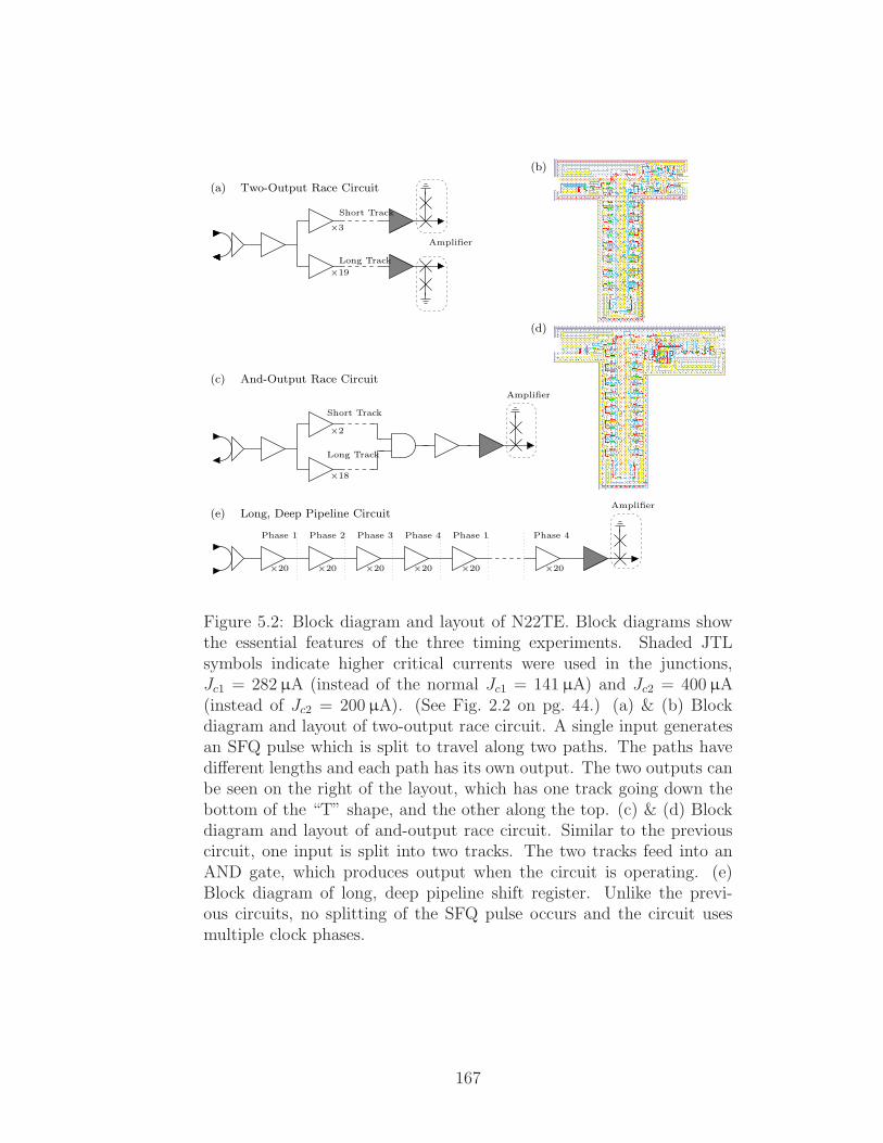
×18
×2
Long Track
Short Track
Amplifier
Amplifier
×3
×19
Long Track
Short Track
Phase 1 Phase 1Phase 2 Phase 3 Phase 4
×20 ×20 ×20 ×20 ×20
Phase 4
×20
Amplifier
(d)
(a)
(e)
Two-Output Race Circuit
(c) And-Output Race Circuit
Long, Deep Pipeline Circuit
(b)
Figure 5.2: Block diagram and layout of N22TE. Block diagrams showthe essential features of the three timing experiments. Shaded JTLsymbols indicate higher critical currents were used in the junctions,Jc1 = 282µA (instead of the normal Jc1 = 141µA) and Jc2 = 400µA(instead of Jc2 = 200µA). (See Fig. 2.2 on pg. 44.) (a) & (b) Blockdiagram and layout of two-output race circuit. A single input generatesan SFQ pulse which is split to travel along two paths. The paths havedifferent lengths and each path has its own output. The two outputs canbe seen on the right of the layout, which has one track going down thebottom of the “T” shape, and the other along the top. (c) & (d) Blockdiagram and layout of and-output race circuit. Similar to the previouscircuit, one input is split into two tracks. The two tracks feed into anAND gate, which produces output when the circuit is operating. (e)Block diagram of long, deep pipeline shift register. Unlike the previ-ous circuits, no splitting of the SFQ pulse occurs and the circuit usesmultiple clock phases.
167

0 0.2 0.4 0.6 0.8 1 1.2 1.4
φ[rad
]
t [ns]
Input
Short Track
Long Track Delay Difference
0
2π
0
2π
0
2π
Figure 5.3: Plot of the input and output phases versus time for the two-output race circuit shown in Fig. 5.2(c). This figure shows the inputphase of the first and last junctions in the two-output race circuit, assimulated in Spice for Hypres 4.5kA/cm2 process at 4 GHz. The inputshows the phase rise and fall with SFQ pulse pairs. The short trackshows an output almost immediately after the input junctions switch.The long track takes noticeably longer. This timing difference betweenoutput from the short and long tracks is the delay difference betweenthe two positive SFQ pulses.
clock line path length difference is approximately 1200µm, the delay in the clock
line between the two paths is approximately 12 ps. At 5 GHz the wavelength is
approximately 2 × 104 µm. The change in wavelength over the size of the circuit
is approximately 6% at the maximum operating frequency. There is always an
unknown delay introduced by the output cables. However this difference in delay is
constant and can be subtracted out from the measurement data.
Figure 5.4 shows predicted timing behavior in this experiment as a function
168

of input phase as found from (3.8). There are three curves showing output phase
delay for the path with 1, 8 and 20 JTLs (or 2, 16, and 40 Josephson junctions,
respectively), and also a curve showing the accumulated output delay between long
and short paths. One can see that the cutoff point of the input phase is dominated
by the longer path and that the time delay difference between long and short paths
is fairly constant until the phase approaches the timing limit, at which point it
sharply increases. This time delay difference can be measured in a real device as a
function of input phase by adjusting the phase of the data relative to the clock.
Figure 5.4 shows the difference in timing behavior for both short and long
paths. Three points are worth noting in this graph: (1) the cut-off point is dominated
by the long path, for obvious reasons; (2) the timing difference is fairly constant until
the phase reaches close to the timing limit, at which point it sharply increases; and
(3) the delay flattens out at θ = 0. These qualitative features should be readily
observable in the actual data
5.2.2 Simulation of Experiment 2 — And-output Race Circuit
The second experiment was similar in concept to the first experiment in that
it also measured relative delay between a short and long path. The same number
of junctions is used in the short and long track. However, instead of observing
the delay on the oscilloscope it was sampled by an AND gate. This experiment
eliminates the uncertainty in measuring picosecond-scale delays on the oscilloscope.
The AND gate compares the relative timing of the pulses — modulated by one
169

0
0.2
0.4
0.6
0.8
1
1.2
1.4
1.6
1.8
0 0.5 1 1.5 2 2.5 30
20
40
60
80
100
120
0 20 40 60 80 100 120 140 160 180 200
OutputPhaseDelay
ν(θ)[rad]
OutputTim
eDelay
[ps]
Input Phase θ [rad]
Input Time [ps]
2 JJs
16 JJs (short)
40 JJs (long)
Difference betweenshort and long
Figure 5.4: Two-output race circuit timing predictions. Output phasedelay calculated from (3.8) of the JTL circuit in Experiment 1 for Hypres4.5 kA/cm2 process at 2.5 GHz, with two parallel paths — short with 8junctions total and long with 40 junctions total. Different curves showthe phase delay as a function of input phase for 2 JJs, 16 JJs, and 40JJs on a single phase. Paths with more junctions take longer. The redsolid curve shows the expected difference in accumulated delay betweenlong and short path.
clock period — and produces binary data. If two delayed pulses come within the
same clock window, then the AND gate output is “one”’ and otherwise the output
is “zero”. By changing the the amplitude of the bias current, I can modulate the
AND output and observe the operation of the circuit for different input phases.
Figure 5.5 shows the expected regions with output and without output from
the AND gate for this experimental circuit, calculated from (5.3b) and plotted for
different frequencies. These calculated curves on the plot are derived from the
170
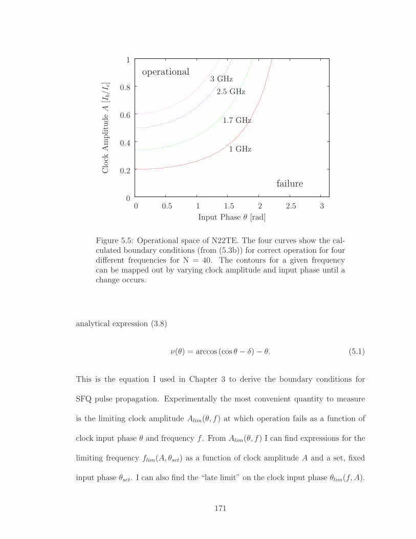
0
0.2
0.4
0.6
0.8
1
0 0.5 1 1.5 2 2.5 3
Clock
AmplitudeA
[Ib/I
c]
Input Phase θ [rad]
operational
failure
1 GHz
1.7 GHz
2.5 GHz
3 GHz
Figure 5.5: Operational space of N22TE. The four curves show the cal-culated boundary conditions (from (5.3b)) for correct operation for fourdifferent frequencies for N = 40. The contours for a given frequencycan be mapped out by varying clock amplitude and input phase until achange occurs.
analytical expression (3.8)
ν(θ) = arccos (cos θ − δ)− θ. (5.1)
This is the equation I used in Chapter 3 to derive the boundary conditions for
SFQ pulse propagation. Experimentally the most convenient quantity to measure
is the limiting clock amplitude Alim(θ, f) at which operation fails as a function of
clock input phase θ and frequency f . From Alim(θ, f) I can find expressions for the
limiting frequency flim(A, θset) as a function of clock amplitude A and a set, fixed
input phase θset. I can also find the “late limit” on the clock input phase θlim(f, A).
171

The boundary condition is determined from (3.8) by the criteria
δ − 1 < cos θ, (5.2)
where δ = 6πft0/A. This criteria corresponds to the case where the SFQ pulse
arrives too late in the clock cycle to switch the junction. I expect these equations to
give a very good approximation to the boundary conditions of SFQ pulse propaga-
tion in the limit of frequencies where the pulse timing fitting parameters are close to
unity (see Section 3.3, page 95). (In the general case where the pulse timing fitting
parameters are not close to unity, the simulation would need to iteratively calculate
the next output based on the previous input, using the fitting parameters.) Solving
(5.2) for θ, f , and A gives the expected behavior:
θlim(A, f) = arccos(2πNt0f
A− 1), (5.3a)
flim(A, θset) =1 + cos θset
2πNt0A, (5.3b)
Alim(f, θset) =2πNt0
1 + cos θsetf, (5.3c)
with θset now a variable in operational space instead of the input phase. These
three equations define the boundaries in operational space between successful pulse
propagation and failure. From (5.3a)–(5.3c), one can see that for a given frequency
there exists a minimum amplitude and a maximum phase input. As the frequency
increases, the operational range decreases. All frequencies have a common upper
limit on amplitude at A = 1, after which failure occurs due to overdriving of all
junctions. This failure mechanism is unrelated to frequency or clock phase.
Coming back to Fig. 5.5, each curve divides the the operating space into regions
where pulses propagate — above the curve — and regions where the pulses do
172

not propagate — below the curve. Notice that for a given clock amplitude, the
operational space for correct operation grows as frequency is decreased. That is, for
slower clock frequencies the pulses may arrive later without preventing operation.
For a given clock input phase, the clock amplitude can also decrease as the frequency
decreases. Pulses arriving before θ = 0 are not allowed (in this model) and at A > 1
a different failure mechanism takes over (all junctions switch regardless of input).
5.2.3 Simulation of Experiment 3 — Long Shift Register
I designed the third circuit to verify the effect of phase boundaries on timing
stability and check the maximum operating frequency of an RQL circuit. Instead of
trying to measure an RQL circuit in the 20 to 40 GHz range — which is challenging
experimentally — I decided to design long, deep pipeline shift registers with 20
JTLs per stage. In this case, the maximum operating frequency from simulation
was expected to be 5 GHz at maximum clock amplitude (A = 1). The timing
behavior of this shift register is equivalent to a short shift register operating at
100 GHz with pipeline depth of one JTL. This follows from the definition of δ. In
addition, this experiment allowed me to check the self-correcting behavior of an
RQL circuit by measuring the clock power margins as a function of input phase.
The detailed circuit schematic of the shift register is shown in Fig. 5.6; there are
1384 junctions and 40 junctions per phase, which gives 20 JTL segments per phase.
The long length ensured that practically any phase delay introduced at the
input would be corrected by the time output occurs. The testing equipment (see
173

Four phases, 1384 Junctions
20 JTLsAmp
Phase 0020 JTLsPhase 00
20 JTLs 20 JTLs 20 JTLsLaunch
Phase 01 Phase 10 Phase 11
Figure 5.6: Long, deep pipeline shift register. Schematic of the long, deeppipeline shift register used in Experiment 3. (Intermediate stages areomitted for clarity.) Each phase contains 20 JTLs with 40 junctions, apipeline depth designed to fail at f = 5GHz and A = 1. Unlike previousexperiments’ circuits, this circuit has a four-phase clock with 80 JTLsper cycle, for a total of 17.25 full clock cycles of delay through the circuit.Two extra junctions from a squid and serve as output amplification atthe output.
Section 4.4.1 on pg. 157) only worked up to a speed of about 6 GHz, and the circuits
were designed to fail below this speed for maximum clock amplitude. Similar to
the other two circuits, the final JTL in the shift register had critical currents of
Jc1 = 282µA and Jc2 = 400µA. This was the only circuit on N22TE that I tested
with two clock lines and four clock phases; the previous circuits only had one phase
on a single AC clock line and one DC flux offset line. The phase difference between
the clock lines was controlled externally (see next Section).
5.3 Experimental Setup
Figure 5.7 shows a block diagram for the experimental setup, which has been
reproduced from Fig. 2.14 in Chapter 2. However, the initial settings for the circuits
was different. I obtained the optimal operating point under the assumption that
174
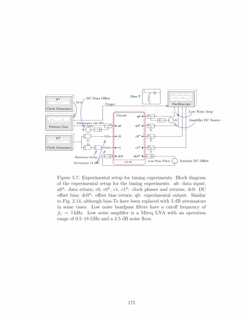
+
+
+Attenuator (3 dB)
c1 c1*
a0*a0
c0 c0*
dc0 dc0*
q0Circuit
Junction DC OffsetHardware Delay
Trigger
4.2 K
ρ2
Bias-T
Low-Pass Filter
ρ1
Low Noise Amp
Amplifier DC Source
Sync
DC Data Offset
Attenuator (40 dB)
Oscilloscope
Clock Generator
Pattern Gen.
Clock Generator
#2
#1
Figure 5.7: Experimental setup for timing experiments. Block diagramof the experimental setup for the timing experiments. a0: data input;a0*: data return; c0, c0*, c1, c1*: clock phases and returns; dc0: DCoffset bias; dc0*: offset bias return; q0: experimental output. Similarto Fig. 2.14, although bias-Ts have been replaced with 3 dB attenuatorsin some cases. Low noise bandpass filters have a cutoff frequency offC = 1 kHz. Low noise amplifier is a Miteq LNA with an operationrange of 0.5–18 GHz and a 2.5 dB noise floor.
175

the margins on clock amplitude, input phase, and relative clock phase are indepen-
dent. To find the margins on amplitude, I first turned the amplitude down to near
failure. I then changed the clock phase up and down to find preliminary margins on
the phase. The clock input phase could be searched easily by introducing a small
frequency difference between the two clock generators. At the middle of the phase
range I then turned the clock amplitude down until I found the lower bound of the
clock amplitude. At the same input phase, I next increased the amplitude until fail-
ure. The optimum amplitude is assumed to be the geometric mean between clock
amplitudes. To establish the optimum relative clock phase, I set the amplitude at
its optimal value and then decreased the relative phase until failure, increased it
until failure, and chose the mean value as the optimal operating value.
Table 5.1 shows the operating conditions I found for the circuits’ dc bias cur-
rents it tests on the chip. The nominal operating point was reasonably close to
the design values, indicating good correspondence between designed and as-built
parameters. To ensure margins on the bias currents were adequate, I checked that
each was close to midway between the maximum and minimum limit currents while
the circuit was at its optimal operating point.
Each of the three experiments allowed me to test the timing behavior as a
function of phase delay between clock and data input. To take data, I initially
reduced the clock phase until failure occurred, even with the clock amplitude at
the maximum value. Then I increased the clock phase in small increments. At
each increment, I measured the high and low values of clock amplitude (in dBm).
Failure on the high end was clear to observe — all digital output read “one.” At
176

Table 5.1: Operational bias conditions for N22TE. The nominal valuesare close to the design values. The minimum and maximum rangesshow that the circuit is operating without major fabrication issues. Thea0 input voltage range is approximate. The DC Data Offset value isdependent on the input data pattern; the value here is for a pseudo-random data pattern.
Input Nominal Minimum Maximum Design
Amplifier DC Source 175µA 100µA 226µA 168µADC Data Offset 80µA 27µA 187µA (n/a)dc0 2 mA 0 mA 4 mA 2 mAa0 (with 40 dB attenuator) 1 Vp−p 0.5 Vp−p 1.75 Vp−p 1 Vp−p
low amplitudes, the circuits start to produce random errors that result in gradually
decreasing voltage levels in sampling measurements on the oscilloscope and flickering
measurements for non-sampling measurements. Failure was defined as the clock
amplitude at which an increase of +0.1 dBm input to the clock power produced no
change in the output signal. Under this condition, the logical operation of the circuit
remains the same with a further increase in clock power, i.e. the circuit is operating
correctly. When the change in clock power produces a change in the output signal,
some part of the circuit is not operating fully correctly.
5.4 Data and Analysis
For the time difference measurements, I define the delay as the difference in
output time ∆t between the midpoints of two output pulses as measured by the user-
adjustable markers on the oscilloscope. I also checked the output for feedthrough or
line-to-line coupling by turning off the output bias current. To determine coupling
between output and clock lines I turned the bias on and off to observe the change
177

in output voltages.
5.4.1 Experiment 1 Results — Two-output Race Circuit
Figure 5.8 shows the main experimental results from Experiment 1 on the
two-output race circuit. The measured timing difference (filled circles) are plotted
as a function of the input phase offset. The error bars correspond to the resolution
of the oscilloscope. The first thing to notice is that the circuit works over almost
the entire clock cycle. This is a surprise because the analytical model given by (3.8)
and the VHDL model define operating regions that start from the beginning of the
clock window, which is one-third of the clock period or a phase. One implication
of this plot is that positive SFQ pulses arriving during negative clock bias wait at
the JTL until the bias current reaches the critical value for propagation. In this
circuit the delay of the short JTL is approximately constant, whereas the delay of
the long JTL is far more dependent on the input clock phase. This suggests that
the slight variations in the phase delay below 2.5 rad are due to the long line. The
small maximum near 2.5 rad corresponds to θ = 0 input phase relative to the clock.
For larger offsets (beyond 2.5 rad) the behavior follows the predictions of (3.8) (see
red curves shown in Fig. 5.4). The timing was fairly even until the largest phase
offsets, where the timing difference quickly increased before failing.
For the first experiment, I used the oscilloscope to find the output times of two
pulses. The delay of the equipment (probe, wires, etc.) was unknown but assumed
to be constant. (They need not be the same for both pulses because any constant
178

0 1 2 3 4 5 6
∆t[ps]
θin [rad]
20 ps
0.5 GHz
1.0 GHz
1.5 GHz
Figure 5.8: Two-output race circuit measured data. Measured timingdifference ∆t between outputs from short and long JTL paths for severaldifferent frequencies plotted as a function of input phase θin. θin isrelative to the first recorded data point. The blue (dashed) curve is afit of (5.4a) to all data points. The red (solid) curve is a fit of (5.4a)to the points at large phase offset where (3.8) is valid. The range ofphase delays that result in SFQ propagation were considerably largerthan predicted by (5.3c). The sharp upturn of the phase delay closeto failure was a prediction of (5.3c) that was verified here. Figures areoffset for clarity. The delay includes a contribution from the delay of thecoaxial lines in the probe, making only a relative measurement of thetiming difference possible.
179

term will produce an offset but otherwise not affect the results.) The expected
relationship for the timing output of a pulse is given by (5.1). Since I was looking
for the timing difference, the results were expected to be of the form
∆ν(θ) = νlong(θ)− νshort(θ)
= arccos(cos θ −Nlongδ)− arccos(cos θ −Nshortδ). (5.4a)
In practice, I tried fitting to a function of the form
∆ν(θ) = γ4γ1[arccos(cos(θ + γ2)−Nlong δ/γ1)−
arccos(cos(θ + γ2)−Nshort δ/γ1)] + γ3, (5.4b)
where δ = 3ωt0/A (as defined in Chapter 3), Nshort and Nlong are the number of
junctions in the short and long paths, respectively, and γ1, γ2, γ3, and γ4 are fitting
parameters. Ideally I expected γ1 = γ4 = 1; γ2 and γ3 merely allow for the unknown
offset due to the unknown length of the electrical lines. The parameters of particular
interest are γ1 and γ4, which are related to the curvature and stretching of the curve.
These factors are similar to those found in Chapter 3. Although I will shortly show
two ways in which the clock amplitude could be determined, for this experiment the
clock amplitude was still an unknown but it was not critical to the measurements at
hand. Likewise, as I discovered in Chapter 3, the effective value of δ could change in
real circuits due to leakage currents from adjacent JTLs and gates. The parameters
γ2 and γ3 have no restrictions and account for the systematic uncertainty in the
absolute phase and delay, respectively.
I plotted two different fits in Fig. 5.8 corresponding to (5.4b) with different
fitting ranges. The red (solid) curve is analogous to the timing difference curve
180

Table 5.2: Fitting parameters of two-output circuit data. γ1 and γ4 wereexpected to be close to unity, but are still within the ranges of analogousparameters found by fitting simulations in Chapter 3. Compare to TableB.1. γ2 and γ3 merely account for systematic constant phase offset un-certainty in the experimental setup and carry no particular significance.
0.5 GHz 1.0 GHz 1.5 GHz
Red Fit
γ1 1.0635 0.6677 1.5924γ2 -2.5064 -2.4101 -2.9371γ3 37.4684 67.2539 49.6685γ4 0.5821 0.8502 0.2378
Blue Fit
γ1 5.2273 0.6677 8.4889γ2 -2.1259 -2.4101 -2.5474γ3 48.1487 67.2539 49.6719γ4 5.3251 0.8502 4.078
shown in Fig. 5.4, which starts at θ = 0. The blue (dashed) curve fits the same
function to the entire data range. As one can see in Fig. 5.8 there is a very good
fit to the experimental data. The fitting parameters are given in Table 5.2. Both
fits are similar to each other and closely follow the measured data. In both cases
the abrupt increase in timing difference at large phase delays was captured by the
function. This qualitatively confirms that the timing behavior is following (5.4b)
but not necessarily (5.4a). The values of the parameters γ1 and γ4 for the red fitting
are closer to unity than those for the blue fit. This is not unexpected as the model
was derived only for θ > 0, whereas the blue curve is fit to data for which θ < 0 as
well.
181

0
0.2
0.4
0.6
0.8
1
0 0.5 1 1.5 2 2.5
Current(I
b/I
c)
Phase θ (rad)
1.0 GHz
1.5 GHz
2.0 GHz
2.5 GHz
Figure 5.9: And-output race circuit data. This figure shows the datafrom Experiment 2 and predictions for the boundary based on (5.3c).Four frequencies between 1.0 GHz and 2.5 GHz are shown. Data between1.0 GHz and 2.0 GHz follows the correct qualitative behavior. The datamatches very closely f or the current limits and somewhat closely for thecurrent limits.
5.4.2 Experiment 2 Results — And-output Race Circuit
Figure 5.9 shows the main results of the And-output race circuit experiment.
The purpose of this experiment was to measure the operational margins of an RQL
circuit as a function of clock frequency, amplitude, and input phase. In Fig. 5.9 I
have plotted input phase θ versus the lower bound of bias current Ib. The points are
measured data, and the curves are predictions based on (3.12) (see pg. 172). This
plot can be compared to Fig. 5.5. The data in Fig. 5.9 is shown for four frequencies
(1.0 GHz, 1.5 GHz, 2.0 GHz, 2.5 GHz). The limiting factor on measurements was
182

the step size of the power of the clock signal generator. With a step size of 0.1
dBm, the error on bias current depends on the bias current A = Ib/Ic and goes as
∆A = A log 10/200. The main observation is that for the 1.0, 1.5, and 2.0 GHz
data, the phase limit is found near the expected value (as the solid curves) from
(5.3b). However, the measured lower current bound occurs at a higher value than
expected. As a result, there is less dependence of the current on clock phase at
the lower measured limits of clock amplitude. Apart from from this, the observed
behavior qualitatively matches the predictions shown in Fig. 5.5.
The cutoff input phase for the three lower frequencies 1.0, 1.5, and 2.0 GHz
matches data to within 5% when one compares the value of the predictions at
Ib/Ic = 1 and the data point with the highest phase θ. However, the cutoff lower
clock amplitude is notably above the values predicted. The data for these three
frequencies shows a specific cutoff for the lower clock amplitude: about 0.25 for 1
GHz instead of 0.175, about 0.35 for 1.5 GHz instead of 0.25, and about 0.5 for 2.0
GHz instead of 0.35. Instead of a gradual decrease in minimum current, it seems a
different effect may take over the lower clock amplitude limit.
In the model, at the lowest clock bias values the junctions just barely manage
to switch in time. The model considers only single junctions in isolation. In real
circuits, junctions are coupled to each other through inductors. In particular, at
phase boundaries, junctions on one side of the phase boundary will influence junc-
tions on the other side (this can be seen in Fig. 1.12). Although the distribution of
current is set by the choice of inductance values in JTL units on phase boundaries,
this additional coupling is still present, adding an additional resistance to switching
183

of the last junction on a phase. The result is that additional “torque” needs to be
applied to the junction in order for it to switch. However, for later input phases,
the bias current on the next phase will already be higher, thus making it easier for
junctions on both sides of the phase boundary to switch. Hence, the effect goes
away after a certain input phase.
For this experiment, I had to determine the bias A = Ib/Ic from the measured
clock output. The mean power in dBm for a given measured peak-to-peak voltage
Vp−p can be found from
PdBm = 10 log10
(V 2p−p
8× 50Ω
1000
W
)
, (5.5)
where the factor of 8 is necessary to convert the peak-to-peak voltage into a root-
mean-squared value, 50Ω is the internal impedance of the oscilloscope, and the
factor 1000/W defines the dBm unit. The test setup (see Fig. 5.7) was symmetric
between input and output with the exception of the power splitter on the clock
output (which had a loss of approximately 6 dB) and any attenuators placed on
the probe. If we account for all power attenuators on the clock lines with a factor
Pattenuator , the power delivered to the circuit on-chip Pchip is related to the input
power Pin and output power Pout at the oscilloscope by
Pchip =1
2(Pin − Pattenuator + Pout), (5.6)
where all values are in dBm. (The factor of 1/2 is due to the square root in the
geometric mean when going from linear to log scale.) We can then express the
current Ib induced in a the bias inductor as
Ib =M
L
√
2Pchip
Zclock=M
L
√2
1000× Zclock10(Pin−Pattenuator+Pout)/20, (5.7)
184

Table 5.3: Summary of measurements of Pin and Vp−p in N22TE usedfor calibration of the junction bias current Ib. Pattenuator is the amount ofattenuation found between the clock signal generator and the chip that isnot found between the chip and the oscilloscope. Pout is calculated fromVp−p by (5.5). Pchip is calculated by (5.6), and given in both dBm andmW. Ib (total) is calculated using (5.7). Ib (JJ1) and Ib (JJ2) are calcu-lated as fractions of Ib (total) based on the distribution of supercurrentsthrough two parallel inductances (see Fig. 2.2). The attenuator shownin Fig. 5.7 was measured to have an attenuation of 2.83 dB. Calibrationof the circuit to a known current of Ib = Ic gives an additional factor of1.75 (or 2.43 dB) to current due to attenuation.
f (GHz) 1.0 1.5 2.0 2.5 2.5 GHz
Pin 3.4 5.1 5.3 5.5 5.7 dBmVp−p 81.1 84.9 82.2 74.6 76.2 mV
Pattenuator 5.26 5.26 5.26 5.26 5.26 dBmPout -17.840 -17.442 -17.723 -18.566 -18.382 dBmPchip -9.850 -8.801 -8.842 -9.163 -8.971 dBmPchip 0.104 0.132 0.131 0.121 0.127 mW
Ib (total) 0.221 0.250 0.248 0.239 0.245 mAIb (JJ1) 91.072 102.761 102.285 98.570 100.775 µAIb (JJ2) 130.103 146.802 146.122 140.815 143.965 µA
where M is the mutual inductance of the RQL clock-line transformer, L is the bias
inductor, and Zclock is the clock line impedance (by design about 32Ω). Equation
(5.7) can be checked at a known reference point where Ib = Ic and the actual
attenuation can be found.
Equation (5.7) was fundamental to the second experiment because I needed
to find the input phase at known clock amplitudes. The highest working clock
amplitude was very consistent and represented a failure mechanism independent of
the input phase. This power set the baseline for the critical current though the
junction. Using this as a reference point, I then found the current through the
185

junction from
Ib = Ic(10∆P/10
)1/2(5.8)
with ∆P = Phigh − Plow, the difference in measured values for the high and low
clock power values, respectively. This method avoided the effects of uncertainties in
measurements of Vp−p, as well as the effect of losses in the probe, losses in devices,
and the uncertainties in values of mutual and linear inductances. Furthermore,
(5.8) and (5.7) give independent estimate for the critical current, and these values
matched within the uncertainty of the attenuation of the clock splitter, which is
about 12%. Table 5.3 shows results from this analysis of the data.
The main result is that calibration suggests a loss of 2.43 dB in power before
reaching the chip. The measured attenuation of the 3 dB attenuator was actually
2.83 dB, which is within the tolerances of the device. The average currents Ib
(JJ1) and Ib (JJ2) should be as close to their design values of 100µA and 141µA as
possible. This occurs for Pattenuator = 5.26, leaving a remaining 2.43 in unaccounted-
for attenuation. This extra attenuation is likely found in the variable delays ρ1 and
ρ2.
In conclusion, the results from the and-output race circuit experiment quali-
tatively matched the predictions of the analytic timing model. In principle, there
were clear cutoff values for both the clock current amplitude and the input phase
and the margins shrank as the frequency was increased. The cutoff values approxi-
mately matched with the predictions from (5.1). However, whereas the predictions
were for gradual transitions from one limit to the other, the measured data had a
186

0
0.5
1
1.5
2
2.5
3
-2 -1.5 -1 -0.5 0 0.5 1 1.5 2
Clock
Pow
erMargins[dB]
θ [rad]
2.5 GHz
2.0 GHz
1.5 GHz
1.0 GHz
Figure 5.10: Multi-phase shift register clock amplitude margins plottedversus input phase for four frequencies. The data has been centeredat zero phase. The sharp drop in margins at either end confirmed theexpected behavior of a long, deep pipeline shift register. For |θ| < 1.5 radthe clock margins generally show less than 0.2 dBm variation. Maximumclock amplitude was 4.5 dBm (measured) for all frequencies.
more abrupt and earlier cutoff. Also, at a clock frequency of 2.5 GHz, the data did
not fit the predictions. Nevertheless, there was still an increasing minimum clock
amplitude with increasing frequency.
5.4.3 Experiment 3 Results — Long, Deep Pipeline Shift Register
Figure 5.10 shows my main results from tests of the long, deep pipeline multi-
phase shift register. In this figure I plot the clock margins versus the input phase.
The power margins show a small variation over a range of ±1.5 radians. The rapid
187

decline in clock margins at either extreme indicates rapid failure of the shift register.
These wide margins confirm the main results of Experiment 1, in which I found the
pulse propagation window extended well beyond that assumed by the model. I note
also that as the clock frequency increased the nominal clock power margins decrease.
The primary goal of this experiment was to measure the junctions switching
time parameter t0. At failure, δ =√2 and using the definition of δ we can express
the baseline switching time as
t0 =A
3√2πfN
, (5.9)
where N = 40 is the number of junctions in each clock phase of the long, deep
pipeline shift register in N22TE and A is the experimentally determined clock cur-
rent amplitude in units of Ic. Table 5.4 shows the results of my analysis of the data,
using the nominal clock power measurements shown in Fig. 5.10 and taking into
account the calibration from Experiment 2. The average value for t0 is 0.44 ps, with
20% variation between measurements at different frequencies. This compares well
with the value of 0.44 ps expected from the IcRN product 0.75 mV and application
of (3.7). Equivalently, the equivalent IcRN value from t0 = 0.44 ps is 0.77 mV, close
to the 0.75 mV assumed in design.
A secondary goal in testing the multi-phase shift register was to observe if
there was any shift in the output timing as a function of input phase. No such
shift was observed. Only at the very ends of each range was there a noticeable
change in the power margins. Thus, these results showed that long pipelines with
“slow” clocks could adequately propagate SFQ pulses. Similarly, from the 2.5 GHz
188

Table 5.4: Analysis of the long, deep shift register from N22TE. Esti-mated parameters for results of the junction switching time of the long,deep pipeline shift register experiment. f is the clock frequency; Pin isthe displayed value of power on the clock generator; Pout is the mea-sured output from the chip; Pchip is the calculated power delivered to thechip within the ‖θ‖ < 1.5 rad limit; Ib/Ic is the minimum bias currentcalculated from Pchip using (5.8); t0 is calculated using (5.9); and IcRN
is calculated using (3.7). The average value of t0 is 0.440 ps. Averagevalue of IcRN is 0.770 mV. Both values have an uncertainty of about20%. The value of IcRN used for design was assumed to be 0.75 mV.
f 1.0 1.5 2.0 2.5 GHz
Pin 4.500 4.500 4.500 4.500 dBmPout 1.800 2.400 2.700 4.100 dBmPchip 2.700 2.100 1.800 0.400 dBIb/Ic 0.307 0.352 0.378 0.521t0 0.576 0.441 0.354 0.391 ps
IcRN 0.570 0.744 0.926 0.839 mV
maximum operating frequency measured for 40 junctions per phase, I can conclude
that an RQL circuit with 2 junctions per phase will operate at 50 GHz.
5.5 Conclusions
In this Chapter I described three experiments to test different aspects of the
analytic timing model. With Experiment 1, I examined the applicability of the
model to actual junction switching events. With Experiment 2, I showed that the
experimental limits of RQL circuits mainly follow the pattern predicted by the an-
alytic model. A significant difference was that the data showed an earlier clock
amplitude cutoff, implying that margins decrease in fabricated circuits. In Chapter
6, I examine further the issue of suppressed operating margins . Finally, in Experi-
ment 3 I showed that the long, deep pipeline behavior of RQL circuits matches the
189

timing behavior predicted by the analytic model fairly well. I note that an alternate
analysis in Appendix D shows that a suppressed IcRN , or an increased βc, explains
the upper experimental limit of 2.5 GHz instead of the designed 5 GHz.
190
Chapter 6
Carry-Look Ahead Adder Experiment
6.1 Introduction
In Chapter 5, I described results from three experiments which showed the
applicability of the timing model to simple test RQL circuits. What remains is
to design and test more complex RQL circuits that could be used for practical
applications. In this Chapter, I first describe the design of a digital adder. This
circuit is powered by a Wilkinson power splitter, contains non-local interconnects,
and has a fan-out of four in the chosen architecture. I then describe experiments I
performed to verify operation of the device. Figure 6.1 shows a microphotograph of
the completed circuit, which I designate Norwalk 21 Carry Look Ahead, or N21CLA.
6.2 Circuit Design
A Carry-Look Ahead (CLA) adder adds numbers with a minimum latency. I
chose to build and test a CLA for several reasons. When built in RQL, an 8-bit CLA
contains 815 junctions with non-local interconnects between physically separated
logic gates. This means it is a fairly complex circuit that will provide a fairly hard
operational test for RQL. Also, the effective fanout was four as in a CMOS design.
This was achieved through the use of amplification junctions. These features would
191

5cm
5 cm
Figure 6.1: Photo of N21CLA. Four power splitters (green boxes) were inthe four corners of the chip. Data was input from the bottom and movedinto a shift register (black box) on the middle-right. The CLA (red box)pipeline moved data from right to left. The density of circuit elementsdecreased towards the right. Eight high-fidelity output amplifiers (bluebox) on the left amplified the output signal to measurable levels with avery low bit-error rate. Output was on the left side. (Chips were mirrorimaged from design by the fabrication process.)
192

be essential in any real-world application. Many different CLA architectures exist in
CMOS design. I chose to use the Kogge-Stone architecture [44]. Implementing this
architecture in RQL required me to use the VHDL models of Chapter 3. Needless
to say, correct operation of the CLA depends on getting all the details right. For
example, correct synchronization of clock signals is necessary and thus provided a
secondary test of the Wilkinson power splitter.
6.2.1 Propagate/Generate Logic
As noted above, I chose to build a Carry-Look Ahead (CLA) adder with a
Kogge-Stone architecture for our digital adder demonstration. The CLA is based
on the AndOr operation, making it particularly well suited to a demonstration of
RQL. The CLA reduces latency (and size) by pre-calculating the propagate and
generate signals of each bit being added. The propagate signal P is the OR or XOR
operation between the bits, while the generate signal G is the AND operation, as
follows:
Pi = Ai ⊕ Bi, (6.1)
Gi = Ai · Bi. (6.2)
Both these operations can be performed in one quarter of a clock cycle by the RQL
AndOr gate, including use of JTLs to increase the fanout to four. The carry bit
Ci+1 from any bit-level i is given by
Ci+1 = Gi + (Pi · Ci), (6.3)
where Ai and Bi are the i-th bits of the two binary numbers being added.
193

(c)
P = A P = Ai • Aj
G = (Ai •Bj) + Bi
P G
Ai Aj Bi Bj
GP
A B
G = A •BP = A⊕ B
GP
A B(a) (b)
G = B
Figure 6.2: Carry-Look Ahead elements. The Kogge-Stone Adder archi-tecture uses these three logical elements. Logical operations are shownbelow symbols. Note that each unit contains both a pipe for propagate(P) and generate (G) signals. (a) Simple delay unit. Corresponds toJTL units in RQL. (b) PG generation unit. This unit is the first stepin any CLA and it is used only once at the beginning of each pipeline,changing separate 8-bit signals into PG signals. (c) Carry-Look Aheadgate. Takes four inputs, two each for P- and G-signals, and outputs aP- and G-signal.
Figure 6.2 shows the elements of the CLA adder. Figure 6.2(a) shows a delay
unit, which is simply a JTL. Figure 6.2(b) shows the PG calculation unit that is
necessary at the beginning of every pipeline and corresponds to the AndOr gate.
Finally, the actual summing is done by the unit in 6.2(c), which takes two inputs
each for the propagate and generate signals and generates the output according to
(6.1) and (6.3).
In the Carry-Look Ahead scheme the carry bit is pre-calculated ahead of the
actual sum. Whether or not a given carry will propagate or generate is pre-computed
instead of waiting for the carry signal from lesser bits, as in the ripple-carry adder
architecture. By recursively substituting (6.3) into itself for i → i+ 1, one obtains
the following results for the carries going into the first 3 bits. For example, for a
194

four-bit adder,
C1 = G0 + (P0 · C0), (6.4)
C2 = G1 + (P1 · C1) = G1 + P1 ·G0 + P1 · P0 · C0, (6.5)
C3 = G2 + (P2 · C2) = G2 + P2 ·G1 + P2 · P1 ·G0 + P2 · P1 · P0 · C0. (6.6)
By definition C0 = 0, but (6.4)–(6.6) hold even if we allow C0 6= 0. The importance
of (6.4)–(6.6) is that it shows that the final carry bit C3 can be calculated without
waiting for the calculation of the previous carry bit, as in the ripple-carry adder.
In the CLA scheme addition can be broken into groups of n bits. The group-carry
and group-propagate bits can be passed to the next block of n bits, in which case
C0 6= 0. This branching structure gives the CLA a latency of O(logn) [44], where n
is the number of bits added.
6.2.2 Kogge-Stone Architecture
The specific architecture of the CLA can be optimized for latency, size (tran-
sistor count in CMOS or junction count in RQL), or congestion [38], which is the
number of crossings of data pathways [45]. The Kogge-Stone Architecture [44] has
more crossings than other designs and requires more chip area, but has the fastest
performance [45].
Figure 6.3 shows the generic architecture of an 8-bit Kogge-Stone Adder. The
top row of operations is the pre-calculation of propagate and generate bits. The
following three rows contain calculation units and delay units, each with identical
latency. As the depth increases the number of crossings increases. Between the first
195

B7 A5 B5 A4 B4 A3 B3 A2 B2 A1 B1 A0 B0A6 B6
GP GP GP GP GP GP GP GP
P G P G GPP GP GP G P G P G
P G P G P G P G GP GP GP GP
GPGPP G P GP G P G P G P G
A7
Figure 6.3: Generic Kogge-Stone CLA Architecture. Data flows from topto bottom. Most significant bit on left, least significant bit on right. Redlines indicate P-signal pipelines. Blue lines indicate G-signal pipelines.There are eight pipes and four stages. Latency of the Kogge-Stone ar-chitecture CLA is O(log n), where n is the number of bits added, heren = 8. The longest interconnect can be seen between step 3 and 4, wheremany signal lines jump by 4 pipelines.
and second rows there is one crossing bit path. Between the second and third rows
there are three crossings, and between the third and fourth rows there are seven
crossings. For two four-bit numbers, only the left-most four columns are needed,
and the first three rows. Doubling the number of input bits requires adding only
one additional row of logic gates, while doubling the number of pipes. In this design
the branching structure leading to the O(logn) latency can be seen. However, the
number of additional rows decreases as the number of input bits increases. Other
than the crossings, columns 0–3 and 4–7 are nearly identical, with only a delay being
swapped for a regular adding unit.
I made a number of refinements to the generic Kogge-Stone architecture in
196

our circuit. I designed and synthesized an adder using the RQL gate library of
Chapter 3, optimized for latency. The fan-in and fan-out of each stage of the design
can be changed to increase power consumption but decrease latency. I also had a
choice of the amount of congestion due to crossings. My design included non-local
interconnects. Because the design did not include active transmission lines (a device
which can transmit an SFQ pulse between junctions where the inductance between
junctions L > Φ0/Ic), some of the longer interconnects necessitated multiple delay
units (JTLs) between the logic gates, which increased the latency. Additionally,
RQL circuits have specific fan-in and fan-out requirements for each gate (see Section
2.2 on pg. 42). This leads to an optimization problem between size, congestion, and
power. Remarkably, the design was done by use of CMOS design tools with the
necessary VHDL additions.
The overall design of the CLA is shown in Fig. 6.4. Five sequential clock
phases are shown in different colors and the connections are shown between logic
elements. The branching structure of the Carry-Look Ahead design is shown by the
decreasing number of data paths and the greater distances crossed by the data paths
on the right in the figure compared to the left. The single colored boxes are logic
elements while the long, graduated-color boxes represent delays. In this design, the
critical path contains a non-local interconnect between the third and fourth phases,
the path connecting bit pipeline 3 to pipeline 7. This interconnect spans not only
four bits but crosses nine other data paths. In this design, this connection is made by
three JTL elements (six junctions) and is the longest delay in the circuit. We expect
the timing constraints to be tightest on this particular pipeline. To alleviate this
197

Figure 6.4: Final Carry-Look Ahead Adder design. This figure showsthe synthesized layout of the CLA in schematic form, with sixteenbit pipelines and five stages. Data flows left to right, with the most-significant bit on top and least significant bit on bottom. The five clockphases are shown in color: 1 in blue, 2 in green, 3 in orange, 4 in yellow,and 5 in pink. Solid color elements are logic elements. Graduated-colorelements are delays. Lines between elements are data connections. Thepipeline with greatest timing constraints can be seen between phases 3and 4, the top of three lines. This pipeline crosses nine other data paths.
198

issue, we added a fifth phase to the design, which increased latency but increased
timing margins.
6.3 Experimental Setup
The setup of this experiment is shown in a block diagram in Fig. 6.5. This
Figure is similar to Figs. 2.14 and 5.7 with only a few notable differences. There
are eight outputs, labeled q0 to q7, from least-significant to most-significant bit.
Instead of bias-Ts on the clock inputs and outputs, I used 3 dB attenuators in an
effort to reduce reflections and standing waves on the chip. The oscilloscope has
six inputs. With eight data outputs, I decided to monitor one clock output, the
data return from the input, and four of the eight CLA outputs. The other clock
output was terminated with a matched load, as were all CLA outputs not fed into
the oscilloscope. Because of the size of the bias-Ts necessary to apply DC current
to the output amplifiers, no two adjacent outputs could be observed at once. The
Figure shows an example where q1, q3, q5, and q7 are monitored. Observing q0,
q2, q4, and q6 was simply a matter of unplugging the bias-Ts from one port and
plugging them into the others. No additional cool-down was necessary, though the
DC current sources were turned off during the switch. The operating point of the
N21CLA circuit was the same found for the N22TE circuit, shown in Table 5.1.
199

+
++
+
++
Trigger
c1 c1*
a0*a0
c0 c0*
dc0 dc0*
Circuit
Junction DC OffsetHardware Delay
4.2 K
ρ2
Low-Pass Filter
ρ1
Sync
DC Data Offset
Attenuator (40 dB)
Attenuator (3 dB)
Attenuator (3 dB)
q5
q3
q1Low Noise Amp
Source
Amplifier DC
Low Noise Amp
Clock Generator
Pattern Gen.
Clock Generator
Oscilloscope
q0
q7
q6
q4
q2
Bias-T
#2
#1
Figure 6.5: Block diagram of experimental setup for N21CLA. Similar to Fig. 5.7, the same elements present in theexperiments from Chapters 2 and 5 are again found here. Block diagram of the experimental setup for the timingexperiments. a0: data input; a0*: data return; c0, c0*, c1, c1*: clock phases and returns; dc0: DC offset bias; dc0*:offset bias return; q0 – q7: experimental output. Due to space limitations, only four outputs could be observed atonce, and only on non-adjacent ports. Ports not used were terminated with matched impedances (not shown). Lownoise bandpass filters have a cutoff frequency of fC = 1 kHz. Low noise amplifier is a Miteq LNA with an operationrange of 0.518 GHz and a 2.5 dB noise floor.
200

There were four major circuit components on the CLA chip. The Wilkinson
power splitters have been discussed previously in Chapter 4. A stack of 12 SQUIDs
provided amplification of each output signal from the CLA core [46]. Figure 6.6
shows a simplified version of the shift register that was used to send inputs bits to
the CLA. A 16-bit serial shift register provided input to the CLA. With each clock
cycle the data progressed one bit in the shift register and was also inputted to the
CLA. Bits A0–A7 received bits 0–7 from the shift register. Bits B0–B7 received bits
15–8 from the shift register. Note the reverse ordering of the shift register bits for
input B. In Fig. 6.6 I use blue arrows for the A input and red arrows for the B input.
Any 16-bit pattern could be sent in serial form down the input to the shift register
and then applied to the CLA I tested two specific patters. (See Table 6.1). A full test
of the CLA would measure the error rate for many different input patterns. Overall,
the clocks and single data input were arranged in the same fashion described for the
shift register in Chapter 5. (See Fig. 6.5.)
6.4 Experimental Results
I first established the optimum operating point for clock power, relative clock
phase, and data input phase using a procedure that was similar to the procedure
in Chapter 4 for Experiments 1–3. I then tested the digital output of the circuit.
Correct operation was verified by comparing the measured output to the expected
output. Additionally, I measured the power margins for the CLA gates and com-
pared them with simulation results. Finally, I measured the power dissipation of
201

Input (a0)
Shift Register CLA Adder
Output (Bit 0)
Output (Bit 1)
Output (Bit 2)
Output (Bit 3)
Output (Bit 4)
Output (Bit 5)
Output (Bit 6)
Output (Bit 7)
Input Return (a0∗)
Figure 6.6: Shift register input for CLA. The sixteen input bits to theCLA are delivered by an on-chip shift register. Blue arrows representbits of A, red arrows represent bits of B. The input to the register is onthe bottom right and the output on the bottom left. This 16-bit registerpasses the first eight bits to the CLA in reverse order, with the first bitbeing the least significant bit, and passes the last eight bits to the CLAin reverse order, with the 8th bit being most significant.
the CLA core and compared it with the expected dissipation.
6.4.1 Logic Test
The input a0 to the shift register was supplied with two arbitrary patterns of
16 bits each, at a repetition rate of 1/(16f). Table 6.1 shows the two 16-bit input
sequences I used and the expected output from the CLA. The ID number in the
left column is for reference. The columns labeled q7 to q0 are the output bits, from
most-significant to least-significant. The far right column lists the corresponding
202

Table 6.1: Expected CLA output pattern for two cyclic input sequences.This table shows the expected output of each bit of the CLA in sequencein columns. Two short, arbitrary inputs sequences were chosen. Rowsconstitute simultaneous output values. Base-10 decimal numbers aregiven in the right column for reference. ID number on left is for referenceonly.
1111111111111100 1110110111111100
ID q7 q6 q5 q4 q3 q2 q1 q0 D10 q7 q6 q5 q4 q3 q2 q1 q0 D10
0 1 1 1 1 1 0 1 1 251 1 0 1 1 0 0 1 1 1791 1 1 1 1 1 0 0 0 248 1 1 0 1 0 1 0 0 2122 1 1 1 1 0 0 1 0 242 1 1 1 0 0 0 0 0 2243 1 1 1 0 0 1 1 0 230 1 1 0 1 1 1 0 1 2214 1 1 0 0 1 1 1 0 206 1 1 0 0 1 0 0 1 2015 1 0 0 1 1 1 1 0 158 1 0 0 1 1 0 1 0 1546 0 0 1 1 1 1 1 0 62 0 0 1 1 1 0 0 1 577 1 1 1 1 1 1 1 0 254 1 1 1 1 0 1 0 1 2458 0 0 1 1 1 1 1 0 62 0 0 1 0 1 1 0 0 449 1 0 0 1 1 1 1 0 158 0 1 1 1 1 0 1 0 12210 1 1 0 0 1 1 1 0 206 1 0 0 0 0 1 1 0 13411 1 1 1 0 0 1 1 0 230 0 1 0 1 0 1 1 0 8612 1 1 1 1 0 0 1 0 242 0 1 0 1 0 0 1 0 8213 1 1 1 1 1 0 0 0 248 0 1 1 1 1 0 0 0 12014 1 1 1 1 1 0 1 1 251 0 1 0 1 1 0 1 1 9115 1 1 1 1 1 1 0 0 252 0 1 1 0 1 1 0 0 108
203
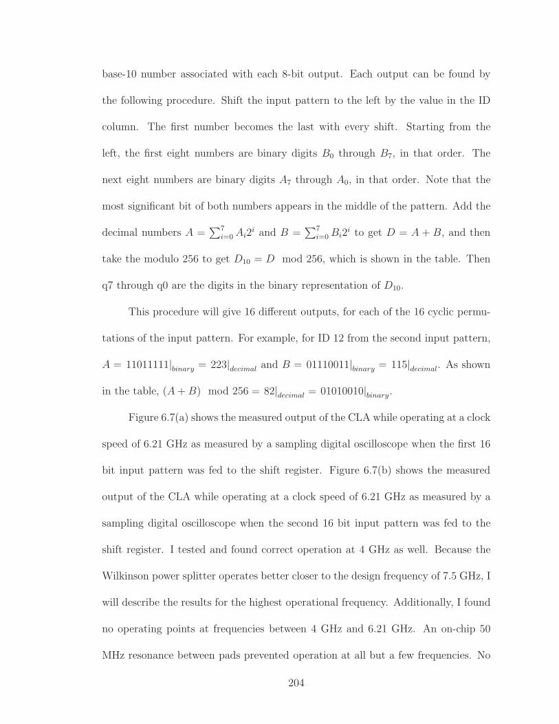
base-10 number associated with each 8-bit output. Each output can be found by
the following procedure. Shift the input pattern to the left by the value in the ID
column. The first number becomes the last with every shift. Starting from the
left, the first eight numbers are binary digits B0 through B7, in that order. The
next eight numbers are binary digits A7 through A0, in that order. Note that the
most significant bit of both numbers appears in the middle of the pattern. Add the
decimal numbers A =∑7
i=0Ai2i and B =
∑7i=0Bi2
i to get D = A + B, and then
take the modulo 256 to get D10 = D mod 256, which is shown in the table. Then
q7 through q0 are the digits in the binary representation of D10.
This procedure will give 16 different outputs, for each of the 16 cyclic permu-
tations of the input pattern. For example, for ID 12 from the second input pattern,
A = 11011111|binary = 223|decimal and B = 01110011|binary = 115|decimal. As shown
in the table, (A+B) mod 256 = 82|decimal = 01010010|binary.
Figure 6.7(a) shows the measured output of the CLA while operating at a clock
speed of 6.21 GHz as measured by a sampling digital oscilloscope when the first 16
bit input pattern was fed to the shift register. Figure 6.7(b) shows the measured
output of the CLA while operating at a clock speed of 6.21 GHz as measured by a
sampling digital oscilloscope when the second 16 bit input pattern was fed to the
shift register. I tested and found correct operation at 4 GHz as well. Because the
Wilkinson power splitter operates better closer to the design frequency of 7.5 GHz, I
will describe the results for the highest operational frequency. Additionally, I found
no operating points at frequencies between 4 GHz and 6.21 GHz. An on-chip 50
MHz resonance between pads prevented operation at all but a few frequencies. No
204
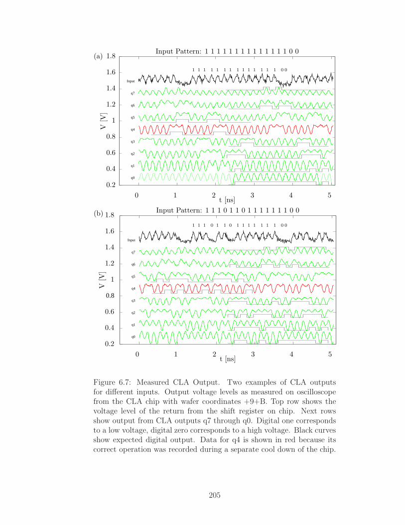
q3
q4
q5
q6
Input
q0
q1
q2
q3
q4
q5
q6
q7
q7
Input
q0
q1
q2
0.8
V[V
]
0 2 3 4 51t [ns]
1.4
1.6
1.8
0.6
0.4
0.2
1
1.2
V[V
]
0 1 2 3 54t [ns]
1 0 01 1 1 1 1 1 1 1 1 1 10 0
Input Pattern: 1 1 1 0 1 1 0 1 1 1 1 1 1 1 0 0(b)
1 0 01 1 1 1 1 1 1 1 1 1 1 1 1
Input Pattern: 1 1 1 1 1 1 1 1 1 1 1 1 1 1 0 0(a)
1.4
1.6
1.8
1.2
1
0.8
0.6
0.4
0.2
Figure 6.7: Measured CLA Output. Two examples of CLA outputsfor different inputs. Output voltage levels as measured on oscilloscopefrom the CLA chip with wafer coordinates +9+B. Top row shows thevoltage level of the return from the shift register on chip. Next rowsshow output from CLA outputs q7 through q0. Digital one correspondsto a low voltage, digital zero corresponds to a high voltage. Black curvesshow expected digital output. Data for q4 is shown in red because itscorrect operation was recorded during a separate cool down of the chip.
205

smoothing or averaging was applied. The top row is the returned input signal. The
eight lower rows are, from top to bottom, the outputs from the most-significant to
least-significant bits.
As in my previous experiments, outputs had inverting amplifiers which made
digital “zero” appear as sustained high output voltages, and digital “one” as low-
dipping voltages. The input return signal was nosier than the CLA output bit it is
not flipped. An input “one” was 1 V with a 36 dB attenuator applied to the chip
and returned without amplification. The eight output bits were amplified on-chip by
the SQUID amplifiers and then the Miteq amplifiers at room temperature. Digital
“zero” and “one” appear as peaks of different height — instead of peaks and flats
— due to crosstalk between data and clock lines carrying a sinusoidal signal. Also,
on this chip, the clock power was eight times greater than I used in my previous
experiments, since each of the eight pipelines required a fully-powered clock line,
and there are eight clock lines per Wilkinson power splitter. Also, crosstalk was
more pronounced for outputs with pads physically closer to the clock signal lines.
Nevertheless, the output was clearly discernible. I made note that the difference in
length of coaxial cables in the probe and from probe to equipment was small, such
that the CLA outputs were not skewed in time relative to each other. An additional
elbow connector used for q4 and q5 introduced the delay seen in Fig. 6.7.
The measured signals (solid curves) shown in Fig. 6.7 correspond to the ex-
pected output (black curves) shown in Table 6.1. The pattern was cyclic and I found
the beginning of the pattern (corresponding to ID 0) by inspection.
206

6.4.2 Operating Margins
Figure 6.8(a) shows the expected power margins based on a spice simulation I
did of the entire CLA (see Appendix F) and Fig. 6.8(b) shows the measured power
margins of the CLA. In the figure, the optimal operating point from measurements
is marked for 6.21 GHz and a clock amplitude of 0.88Ic. This is about 8% above
the 6.21 GHz design value marked in Fig. 6.8(a).
The clock power supplied to the probe was measured using a Agilent E4416A
EMP-P Series Power Meter, and checked against the oscilloscope readings. The out-
put power was measured using an oscilloscope or Hewitt Packard 70620B Spectrum
Analyzer. The power delivered on-chip was then calculated as the geometric mean
of the applied and measured power, or the average value in dBm. Figure 6.8(b)
shows the margins and the optimal operating point for power at 6.21 GHz. The op-
timal power is indicated by the × and is centered between the high and low power
margins. The nominal operating power of -2.4 dBm was found to correspond to the
design power of -2.4 dBm to within 8%. The correct logical operation of the CLA,
along with verification of the designed optimum operating point, also confirms that
the Wilkinson power splitter is operating correctly.
A significant discrepancy with these results is that the predicted margins of 5.5
dB at 6.21 GHz, were much greater than the 1 dB margins I measured. Nevertheless,
the measured optimal operation point of -2.4 dBm clock power was the same as
the design value. The narrowing of the margins is due to microwave effects such as
resonances within the power network (between pads, between splitter and combiner,
207

-7
-6
-5
-4
-3
-2
-1
0
0 5 10 15 20 25
Clock
AmplitudeMargins[dBm]
Clock Frequency [GHz]
Simulated Margins on AndOr Gate(a)
3 dB
1.5 dB
Designed Operating Point
-3
-2.5
-2
-1.5
6.19 6.195 6.2 6.205 6.21 6.215 6.22
Clock
Pow
erMargins[dBm]
Clock Frequency [GHz]
Measured Margins on CLA(b)
Measured Optimal Operating Point
Figure 6.8: Power margins for CLA. (a) Simulation of the CLA (bothpowered and unpowered gate designs) shows the upper and lower powermargins of the gate. The designed operating point of the AndOr gate ismarked at approximately -2.4 dBm. (b) Measured power margins on theCLA in the immediate vicinity of 6.21 GHz. The optimal operating pointis the geometric mean of the power to the chip at high failure and lowfailure. The optimal operating point is marked here at approximately-2.4 dBm.
208
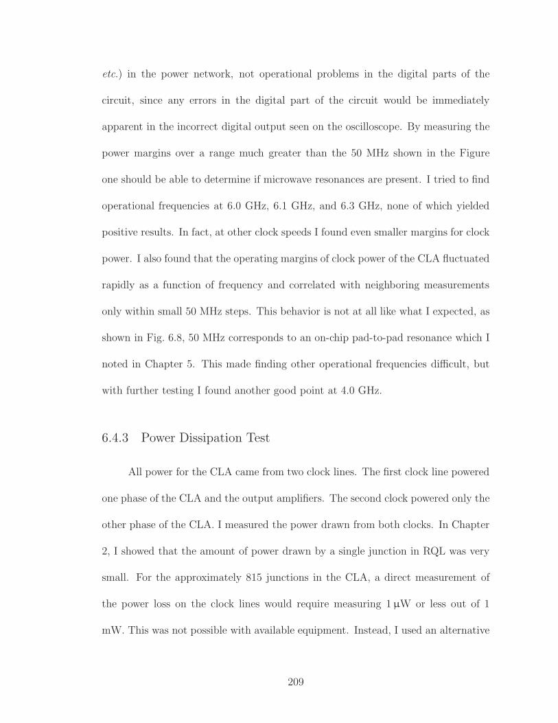
etc.) in the power network, not operational problems in the digital parts of the
circuit, since any errors in the digital part of the circuit would be immediately
apparent in the incorrect digital output seen on the oscilloscope. By measuring the
power margins over a range much greater than the 50 MHz shown in the Figure
one should be able to determine if microwave resonances are present. I tried to find
operational frequencies at 6.0 GHz, 6.1 GHz, and 6.3 GHz, none of which yielded
positive results. In fact, at other clock speeds I found even smaller margins for clock
power. I also found that the operating margins of clock power of the CLA fluctuated
rapidly as a function of frequency and correlated with neighboring measurements
only within small 50 MHz steps. This behavior is not at all like what I expected, as
shown in Fig. 6.8, 50 MHz corresponds to an on-chip pad-to-pad resonance which I
noted in Chapter 5. This made finding other operational frequencies difficult, but
with further testing I found another good point at 4.0 GHz.
6.4.3 Power Dissipation Test
All power for the CLA came from two clock lines. The first clock line powered
one phase of the CLA and the output amplifiers. The second clock powered only the
other phase of the CLA. I measured the power drawn from both clocks. In Chapter
2, I showed that the amount of power drawn by a single junction in RQL was very
small. For the approximately 815 junctions in the CLA, a direct measurement of
the power loss on the clock lines would require measuring 1µW or less out of 1
mW. This was not possible with available equipment. Instead, I used an alternative
209

method of measuring power dissipation that involves measuring the clock sidebands
which appear due to phase and amplitude modulation.
Figure 6.9 shows the measurement of the clock signal using a spectrum ana-
lyzer. The main peak at 6.21 GHz stands well above the noise floor. Sidebands at
6.210 258 GHz and 6.209 742 GHz can clearly be seen in both measurements. The
sidebands are at ±258.75 kHz with respect to the main band, because they were
generated by a cyclic 24,000-bit input sequence containing 12,000 successive “zeros”
and either 12,000 successive random bits or “ones.” The key thing to notice is that
the sideband peaks in Fig. 6.9(a) are higher than the side band peaks in Fig. 6.9(b).
This is because power was drawn from Clock 0 by the output amplifiers than from
Clock 1.
The calculation of the power drawn by the CLA at the optimal operation
point follows in three parts. First, using the results of Chapter 2, Section 2.6.2, I
determine the relative effect of junction switching on phase and amplitude modu-
lation. In Chapter 2, I argued that the expected delay in the clock signal due to
junction switching was 1.4 ps, independent of clock frequency. Since the time period
corresponding to 6.21 GHz is 161 ps, the phase modulation of the signal from one
junction switch is expected to be
∆θ = 2π1.4 ps
161 ps= 0.0546 rad. (6.7)
Because this is the total variation, the expected amplitude of variation of the phase
is half the value given in (6.7) is
gp = ∆θ/2 ≈ 0.0273 rad. (6.8)
210
-100
-80
-60
-40
-20
0
6.2097 6.2098 6.2099 6.21 6.2101 6.2102 6.2103
Pow
er[dBm]
Frequency f [GHz]
258 kHz
∆P = −69.26 dB
Clock 0 (in phase)(a)
-100
-80
-60
-40
-20
0
6.2097 6.2098 6.2099 6.21 6.2101 6.2102 6.2103
Pow
er[dBm]
Frequency f [GHz]
258 kHz
∆P = −79.33 dB
(b) Clock 1 (quad phase)
Figure 6.9: Measured power spectrum of Carry-Look Ahead Adder. Thisoutput from the Agilent spectrum analyzer displays three peaks. Thecenter peak is at the carrier frequency (6.21 GHz) and the two side-bands are at the modulation frequency ±258 kHz from the center peak.Data input was a sequence of 48,000 non-return-to-zero bits, composedof 12,000 return-to-zero random bits followed by 12,000 return-to-zero“zero” bits. (a) shows clock phase 0, (b) shows clock phase 1.
211

Amplitude Modulation
Frequency Modulation
Inactive
Active
Figure 6.10: Modulation of Clock Signal by RQL Gate Operation. Thisfigure shows a clock signal modulated by an input signal consisting ofa sequence of random bits and all zeros. While the CLA is active theimpedance of the clock lines changes, which results in both amplitudeand frequency modulation. This modulation of the clock signal is ameasure of the power drawn by the CLA while operational.
The power dissipation of the circuit is 0.6µW (see Chapter 2, Section 2.6.2) for a
total applied power of 12.5µW [8]. Thus, the variation in power has an amplitude
of
ga = 1− 12.5µW− 0.6µW
12.5µW= 0.0243, (6.9)
which is close to the value of the phase modulation factor gp. Thus, the two effects
are different but we expect them to be of approximately equal strength.
Figure 6.10 shows the behavior of a clock signal while the CLA was at times
active and at times inactive. While active, the loading of the circuit by the switch-
212

ing junctions drew power (decreasing amplitude), the effective inductance of the
transformers changed, and this changed the propagation time (modulating phase).
This modulation can be expressed as
V (t) = V0(1 + ga sinωat) sin[ω0t(1 + gp sin(ωpt)], (6.10)
where V0 is the nominal output voltage, ω0 is the nominal clock frequency, ωa is the
amplitude modulation frequency, ωp is the phase modulation frequency, ga is the
amplitude modulation factor, and gp is the phase modulation factor. For our test
ωa ≪ ω0, ωp ≪ ω0, gp ≪ 1, and ga ≪ 1.
A Fourier decomposition of (6.10) gives the main peak power P0 at ω0/2π and
a sideband power ∆P below P0 at (ω0 ± nωa)/2π, where in is an integer. As |n|
grows larger, the sidebands grow smaller. I am only interested in the first sideband;
sidebands with |n| > 1 are below the noise floor of the spectrum analyzer. A
Taylor series expansion of (6.10) will have three terms of interest. A constant value
representing the main peak power at 6.21 GHz, and two terms at ω0 + ωa: one
representing the effect of amplitude modulation and one representing the effect of
phase modulation. The relative weights of each are 0.53 for ga and 0.47 for gp, which
we can see by comparing (6.8) and (6.7).
To calculate the effect of amplitude modulation, I temporarily set gp = 0 in
(6.10). The relative strength of the effect of phase modulation on the clock is known
from (6.7) and will be accounted for later. The voltage of the clock line as measured
at the output is different while operational (on) and non-operational (off), and can
213
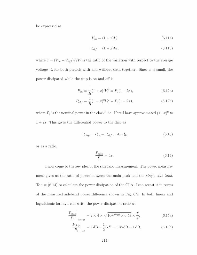
be expressed as
Von = (1 + x)V0, (6.11a)
Voff = (1− x)V0, (6.11b)
where x = (Von − Voff )/2V0 is the ratio of the variation with respect to the average
voltage V0 for both periods with and without data together. Since x is small, the
power dissipated while the chip is on and off is,
Pon =1
R(1 + x)2V 2
0 = P0(1 + 2x), (6.12a)
Poff =1
R(1− x)2V 2
0 = P0(1− 2x), (6.12b)
where P0 is the nominal power in the clock line. Here I have approximated (1+x)2 ≈
1 + 2x. This gives the differential power to the chip as
Pchip = Pon − Poff = 4xP0, (6.13)
or as a ratio,
Pchip
P0= 4x. (6.14)
I now come to the key idea of the sideband measurement. The power measure-
ment gives us the ratio of power between the main peak and the single side band.
To use (6.14) to calculate the power dissipation of the CLA, I can recast it in terms
of the measured sideband power difference shown in Fig. 6.9. In both linear and
logarithmic forms, I can write the power dissipation ratio as
Pchip
P0
∣∣∣∣linear
= 2× 4×√
10∆P/10 × 0.53× π
4, (6.15a)
Pchip
P0
∣∣∣∣dB
= 9dB +1
2∆P − 1.38 dB− 1 dB, (6.15b)
214
where ∆P = 10 log10 x, or the ratio of Pchip to P0 as given in dB, which can be
seen in Fig. 6.9. The terms in (6.15b) require some explanation. In (6.15a), there
is a factor of two for the two sidebands in Fig. 6.10 at ω0 + ωa and ω0 − ωa. There
is a factor of four from the derivation of (6.14). The factor of 0.53 comes from
(6.7) because 53% of the variation is due to amplitude modulation and 47% due to
phase modulation, whereas x is the power ratio taking both effects into account.
Finally, the factor of π/4 is a correction factor due to the data being a square wave
and not a sinusoid, as assumed in (6.10). This last correction is calculated as the
difference in amplitude between the pure sine wave and the fundamental harmonic
of a square wave. Equation (6.15b) follows directly from (6.15a), and is more useful
here because the power measurements are made in dBm.
For eight 32Ω clock lines with 2 mA AC current amplitude passing through
each of the eight clock lines fed from the same input pad, the estimated power to
the chip is
P0 = 8×(2mA√
2
)2
32Ω = 512µW. (estimate) (6.16)
Table 6.2 shows the results of the calculation of Pchip. ∆P is measured from Fig.
6.9. Pchip/P0 is given by (6.15b). Pin and Pout, the clock line input and output
power, and the value of the attenuator on the probe are measured quantities used
to calculate P0. Pchip is calculated from Pchip/P0 from (6.15b) and P0. Because
Clock 0 powers only half the CLA and Clock 1 powers both half the CLA and the
output amplifiers, I estimated the CLA power as twice that being drawn from Clock
0. In the end, this gives the estimated CLA power as 570 nW. This does not take
215

into account power dissipated by the junctions in the shift register, nor the slightly
higher number of junctions powered by Clock 1 than Clock 0. The expected power
for 815 junctions with a weighted average critical current of 162µA (using (2.4))
is P = 1/3 IcΦ0Nf = 563 nW for the CLA at 6.21 GHz. The measurement and
prediction match within 2%, which is remarkable given the many assumptions and
corrections than needed to be made. Finally, I note that this corresponds to only
700 pW per junction, roughly a factor of 200 smaller than CMOS transistors.
6.5 Conclusions
In this Chapter I described an experiment on an RQL CLA that demonstrates
that RQL circuits operate at very low power. At the time of this writing, common
processors typically have 750 million transistors and use over 100 W of power, or
about 130 nW/transistor. The CLA, with 570 nW power dissipation for 815 junc-
tions, uses about 700 pW/junction, i.e. almost 200 times less power per junction
than CMOS uses per transistor. An implication of this experiment is that RQL is
one of the lowest-power digital technologies now known. Additionally, my experi-
ments showed that RQL can be scaled to large, non-trivial circuits and also showed
that RQL was compatible with existing CMOS design and analysis methods.
216
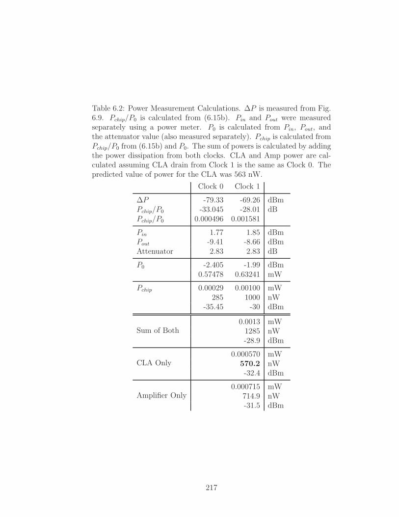
Table 6.2: Power Measurement Calculations. ∆P is measured from Fig.6.9. Pchip/P0 is calculated from (6.15b). Pin and Pout were measuredseparately using a power meter. P0 is calculated from Pin, Pout, andthe attenuator value (also measured separately). Pchip is calculated fromPchip/P0 from (6.15b) and P0. The sum of powers is calculated by addingthe power dissipation from both clocks. CLA and Amp power are cal-culated assuming CLA drain from Clock 1 is the same as Clock 0. Thepredicted value of power for the CLA was 563 nW.
Clock 0 Clock 1
∆P -79.33 -69.26 dBmPchip/P0 -33.045 -28.01 dBPchip/P0 0.000496 0.001581
Pin 1.77 1.85 dBmPout -9.41 -8.66 dBmAttenuator 2.83 2.83 dB
P0 -2.405 -1.99 dBm0.57478 0.63241 mW
Pchip 0.00029 0.00100 mW285 1000 nW
-35.45 -30 dBm
Sum of Both0.0013 mW1285 nW-28.9 dBm
CLA Only0.000570 mW
570.2 nW-32.4 dBm
Amplifier Only0.000715 mW
714.9 nW-31.5 dBm
217


Chapter 7
Summary and Conclusions
7.1 Summary
In the opening to the first chapter, I mentioned that RQL is a superconducting
technology that may eventually replace CMOS technology. It is a classical digital
technology based on encoding classical digital data as decidedly quantum flux units.
Demonstrated RSFQ technologies support the use of SFQ pulses to encode digital
data. However, although RSFQ has many advantages, it is not applicable for many
applications, nor for general purpose processing. An alternative encoding as pulse
pairs gave birth to RQL (see Chapter 2).
Theoretical predictions for RQL estimated a power consumption of approxi-
mately Φ0Ic per junction switching event, which I confirmed in Chapter 2. This,
together with the demonstration of functioning logic gates, opened up the possibility
of large scale integrated RQL digital circuits. RQL logic gates have three or fewer
junctions and are powered through an inductively coupled clock line, removing the
power consumption from dc-biasing resistors. The gates behave as combinatorial
gates on a higher level, but as state machines on a lower, pulse-based level.
In Chapter 3, I examined the detailed behavior of some RQL circuits. The
analytic timing model provides a detailed description of the timing behavior of RQL
junction switching events. Starting from this model, I also derived the self-correcting
219

timing behavior of RQL circuits. Finally, the model also provides estimates on the
limits of operation for the number of junctions per phase, the clock frequency, clock
amplitude, and input time. More than just a useful behavioral model, this analytic
timing model was the basis for a VHDL behavioral model. Together with simulation
results, the VHDL model described RQL circuits in an industry-standard language,
opening up the possibility of applying the large library of existing CMOS design
tools to RQL.
Chapter 4 was focused on developing a suitable power network to supply bias
current to the junctions in an RQL circuit. This power network needed to meet a
number of goals. My primary metric was the current amplitude distribution across
the clock lines. Too much or too little current at any junction would cause improper
operation of the whole chip. Too much variation in the current along the clock
line leads to bad timing properties or a complete failure of the circuit. Because
the clock power has to be pulled back off the chip, using a limited number of pads,
I designed a power splitter/combiner with minimal current variation on the chip,
minimal reflection from the chip, and maximum isolation of different clock lines
on the chip. This was accomplished with a modified set of cascaded Wilkinson
power splitters. The design was collapsed into only six stages with a maximum flat
response, and then this design was optimized using numerical simulations. The test
of two power networks, a 12-stage geometric design to test even mode operation and
a 6-stage maximum flat design to test the odd mode, showed acceptable margins for
the RQL circuit under test.
In Chapter 5, I described three experiments to test the analytic timing model.
220

I directly measured the output timing difference between two pulses on Josephson
transmission lines of different lengths to compare results with (3.8). I measured
the clock power margins as a function of input phase, testing the predictions of the
limits of operation from the analytic timing model. Finally, I measured the clock
power margins of a very long, deep pipeline shift register to directly get an estimate
for the value of t0. The final experiment on a long, deep pipeline shift register gave a
value of the switching time parameter t0 within 2% of the predicted value of 0.47 ps,
but with 20% spread in the measured values. Together, these results demonstrated
that the analytic timing model provides reasonably accurate descriptions of RQL
junction switching behavior.
Finally, Chapter 6 put all previous results together and demonstrated the op-
eration of a practical, integrated RQL circuit. I designed an eight-bit adder using
the Kogge-Stone architecture. It was fully operational at 6.21 GHz with power mar-
gins of 1.5 dB. The device was also operational at about 4 GHz. I found a small
operational regions in clock frequency due to on-chip resonances. The power con-
sumption was predicted to be 563 nW and measured to be 570 nW. For comparison,
a CMOS transistor would be expected to require roughly two orders of magnitude
more power.
7.2 Conclusions and Future Work
RQL began as an alternative to RSFQ. Many of the problems with RSFQ
appear to have been mitigated or absolved by RQL. This thesis has provided some
221

key groundwork for future VHSIC applications of RQL. The timing model has been
shown to be appropriate. The power supply, a limiting factor of modern CMOS
design, is in RQL a matter of designing an appropriate Wilkinson power splitter.
Unlike CMOS, only the power actually used in switching is dissipated on the chip.
The VHDL models of RQL allow the combinational RQL gates to be used in much
the same way as CMOS gates. Finally, the CLA experiment is proof that RQL can
perform digital processing tasks.
Needless to say, despite the progress a number of hurdles remain. The cryo-
packaging of superconducting digital logic of any sort remains expensive and com-
plicated. Though recent advances in this technology may allow superconducting
digital logic to be used in more mainstream applications, it is still a large barrier to
the vast markets served by CMOS technology. Also, the 6.21 GHz clock frequency
demonstrated here is not markedly faster than the current limits of CMOS, around 4
GHz. Although advanced materials promise critical current densities of 10 kA/cm2
— a fourfold increase over the switching speeds displayed here — these processes
are still at an experimental stage. To accommodate the non-local interconnects be-
tween logic elements in the CLA, I had to add an additional clock phase — and thus
latency — to cover the distance. A passive transmission line will solve this issue
but remains untested. In addition, while the RQL gates described here constitute
a universal set, many additional digital elements would be needed to produce the
versatility of CMOS designs. Amongst others, the return-to-zero input requirement
of RQL clashes directly with the non-return to zero patterns in CMOS. To interface
or be compatible to CMOS, RQL must adopt a method of NRZ input.
222

Perhaps the most glaring omission for a fully-functional CMOS replacement
using RQL is memory. While the Set-Reset gate provides a limited memory func-
tionality, contemporary users require vast arrays of memory. The Set-Reset gate
cannot be efficiently scaled up to meet the needs of real data storage. A few possi-
ble solutions may exist. For example, in Chapter 1, I considered only junctions for
which the phase difference between nodes of a junction with zero current was zero.
Other kinds of junctions, π-Josephson junctions instead have a phase difference of
π when no static current flows through the junction. Such exotic junctions can
exhibit hysteretic I-V curves [47], and they can be used to store nonvolatile data.
Implementing such a memory structure in RQL is the topic of ongoing research
[48, 49, 50].
As a practical matter, the number of junctions on a single chip is limited.
While junction counts into the millions have been reported [51], modern processors
may require hundreds of millions of junctions. Scaling of the chip size to accommo-
date hundreds of millions of junctions will be very challenging because of fabrication
errors. Instead, individual chips which each are part of a larger circuit may need
to be fabricated and tested separately, only later to be included as part of a multi-
chip-module.
Finally, all aspect of RQL will benefit from advances in fabrication technolo-
gies. Circuit density is limited by the number of metal layers. The four used here
lead to sometimes convoluted designs when multiple crossings are needed. A six-
layer process may solve some of these issues. Congestion could further be relieved by
adding more layers, such as the 10-layer process developed by Tanaka et al. [52]. In
223

the horizontal instead of vertical direction, smaller lithography sizes will also allow
improvement to circuit density.
7.3 Final Words
Originally conceived as a classical logic family capable of interfacing neatly
with quantum computers and quantum bits, RQL’s strengths make it a viable clas-
sical computer technology in its own right. Many of RQLs advantages are found in
the inherently quantum mechanical behavior of Josephson junctions. Superconduc-
tivity gives rise to the quantization of flux, tunneling gives birth to the behavior of
Josephson junctions, and the Schrodinger equation gives equations of motion which
allow traveling wave solutions. In RQL, these traveling waves are not the solitons
found on individual junctions, but chains of junctions coupled together through
inductors. Unique to RQL, the data is encoded as pairs of pulses, switching junc-
tions back and forth as it travels through the circuit. In this sense, it has aspects
of inherently quantum behavior, but is not quantum computing as it is currently
understood.
RQL is still a technology in its infancy. Many aspects of my work on RQL
have not been mentioned here. Development of the design environment and VHDL
models are ongoing processes. Development of RQL logic gates is an ongoing pro-
cess. Although the combinational behavior of RQL logic gates makes it similar to
CMOS in many ways, CMOS has decades of research and development behind it. If
RQL proves to be even partially as technologically successful as CMOS, there will
224

undoubtedly be many discoveries in RQL in the future.
Although not yet realized, the idea of quantum computation is old enough
to have been studied to a considerable extent in theory. The implications range
from simple computational advantages [53] to world view-changing. As for RQL, it
is in a somewhat unique place. The underlying behavior of the junctions is man-
ifestly quantum, but the output decidedly classical, so RQL in some ways bridges
the behavior between quantum and classical realms. The equations of motion for
a junction are those of a damped pendulum, and yet the behavior of Josephson
junctions is fantastically rich and complex. Perhaps someday RQL will help bring
this complex quantum behavior into everyday use.
225

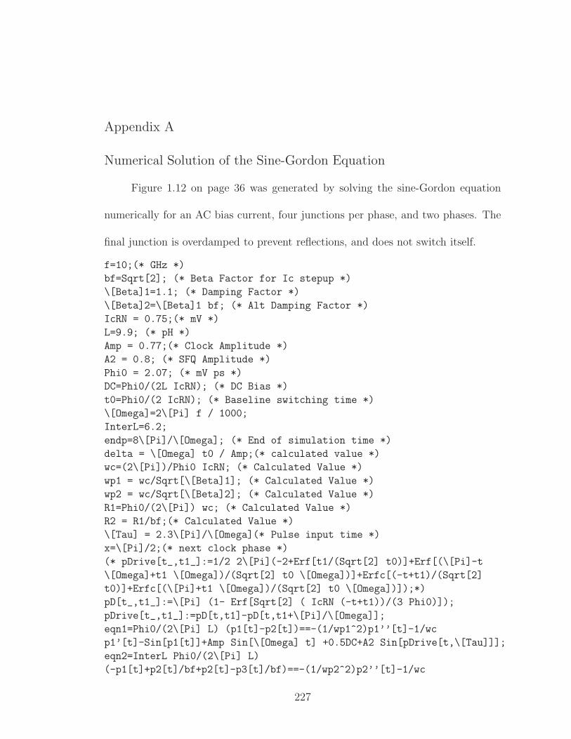
Appendix A
Numerical Solution of the Sine-Gordon Equation
Figure 1.12 on page 36 was generated by solving the sine-Gordon equation
numerically for an AC bias current, four junctions per phase, and two phases. The
final junction is overdamped to prevent reflections, and does not switch itself.
f=10;(* GHz *)
bf=Sqrt[2]; (* Beta Factor for Ic stepup *)
\[Beta]1=1.1; (* Damping Factor *)
\[Beta]2=\[Beta]1 bf; (* Alt Damping Factor *)
IcRN = 0.75;(* mV *)
L=9.9; (* pH *)
Amp = 0.77;(* Clock Amplitude *)
A2 = 0.8; (* SFQ Amplitude *)
Phi0 = 2.07; (* mV ps *)
DC=Phi0/(2L IcRN); (* DC Bias *)
t0=Phi0/(2 IcRN); (* Baseline switching time *)
\[Omega]=2\[Pi] f / 1000;
InterL=6.2;
endp=8\[Pi]/\[Omega]; (* End of simulation time *)
delta = \[Omega] t0 / Amp;(* calculated value *)
wc=(2\[Pi])/Phi0 IcRN; (* Calculated Value *)
wp1 = wc/Sqrt[\[Beta]1]; (* Calculated Value *)
wp2 = wc/Sqrt[\[Beta]2]; (* Calculated Value *)
R1=Phi0/(2\[Pi]) wc; (* Calculated Value *)
R2 = R1/bf;(* Calculated Value *)
\[Tau] = 2.3\[Pi]/\[Omega](* Pulse input time *)
x=\[Pi]/2;(* next clock phase *)
(* pDrive[t_,t1_]:=1/2 2\[Pi](-2+Erf[t1/(Sqrt[2] t0)]+Erf[(\[Pi]-t
\[Omega]+t1 \[Omega])/(Sqrt[2] t0 \[Omega])]+Erfc[(-t+t1)/(Sqrt[2]
t0)]+Erfc[(\[Pi]+t1 \[Omega])/(Sqrt[2] t0 \[Omega])]);*)
pD[t_,t1_]:=\[Pi] (1- Erf[Sqrt[2] ( IcRN (-t+t1))/(3 Phi0)]);
pDrive[t_,t1_]:=pD[t,t1]-pD[t,t1+\[Pi]/\[Omega]];
eqn1=Phi0/(2\[Pi] L) (p1[t]-p2[t])==-(1/wp1^2)p1’’[t]-1/wc
p1’[t]-Sin[p1[t]]+Amp Sin[\[Omega] t] +0.5DC+A2 Sin[pDrive[t,\[Tau]]];
eqn2=InterL Phi0/(2\[Pi] L)
(-p1[t]+p2[t]/bf+p2[t]-p3[t]/bf)==-(1/wp2^2)p2’’[t]-1/wc
227

p2’[t]-Sin[p2[t]]+Amp Sin[\[Omega] t] + DC;
eqn3= InterL Phi0/(2\[Pi] L)
(-p2[t]/bf+p3[t]+p3[t]/bf-p4[t])==-(1/wp1^2)p3’’[t]-1/wc
p3’[t]-Sin[p3[t]]+Amp Sin[\[Omega] t] + DC;
eqn4=InterL Phi0/(2\[Pi] L)
(-p3[t]+p4[t]/bf+p4[t]-p5[t]/bf)==-(1/wp2^2)p4’’[t]-1/wc
p4’[t]-Sin[p4[t]]+Amp Sin[\[Omega] t] + DC;
eqn5=InterL Phi0/(2\[Pi] L)
(-p4[t]/bf+p5[t]+p5[t]/bf-p6[t])==-(1/wp1^2)p5’’[t]-1/wc
p5’[t]-Sin[p5[t]]+Amp Sin[\[Omega] t-x] + DC;
eqn6= InterL Phi0/(2\[Pi] L)
(-p5[t]+p6[t]/bf+p6[t]-p7[t]/bf)==-(1/wp2^2)p6’’[t]-1/wc
p6’[t]-Sin[p6[t]]+Amp Sin[\[Omega] t-x] + DC;
eqn7= InterL Phi0/(2\[Pi] L)
(-p6[t]/bf+p7[t]+p7[t]/bf-p8[t])==-(1/wp1^2)p7’’[t]-1/wc
p7’[t]-Sin[p7[t]]+Amp Sin[\[Omega] t-x] + DC;
eqn8=Phi0/(2\[Pi] L) (p7[t]-p8[t])==-(1/wp2^2)p8’’[t]-1/wc
p8’[t]-Sin[p8[t]]+Amp Sin[\[Omega] t-x] +DC;
s=NDSolve[eqn1, eqn2, eqn3, eqn4, eqn5, eqn6, eqn7, eqn8, p1[0]==0,
p1’[0]==0, p2[0]==0, p2’[0]==0, p3[0]==0, p3’[0]==0, p4[0]==0,
p4’[0]==0, p5[0]==0, p5’[0]==0, p6[0]==0, p6’[0]==0, p7[0]==0,
p7’[0]==0, p8[0]==0, p8’[0]==0, p1, p2, p3, p4, p5, p6, p7, p8,
t,0, endp, MaxSteps-> 100000];
Plot[Amp Sin[\[Omega] t],Amp Sin[\[Omega] t-x],1/(2\[Pi])
Evaluate[p1[t]/.s], 1/(2\[Pi]) Evaluate[p2[t]/.s], 1/(2\[Pi])
Evaluate[p3[t]/.s], 1/(2\[Pi]) Evaluate[p4[t]/.s], 1/(2\[Pi])
Evaluate[p5[t]/.s], 1/(2\[Pi]) Evaluate[p6[t]/.s], 1/(2\[Pi])
Evaluate[p7[t]/.s], 1/(2\[Pi]) Evaluate[p8[t]/.s], , t,\[Tau]-0.2
(2\[Pi])/\[Omega],\[Tau]+1.2 (2\[Pi])/\[Omega], PlotRange-> All]
Plot[Amp Sin[\[Omega] t],Amp Sin[\[Omega] t-x],1/(2\[Pi])
Evaluate[p1[t]/.s], 1/(2\[Pi]) Evaluate[p2[t]/.s], 1/(2\[Pi])
Evaluate[p3[t]/.s], 1/(2\[Pi]), 1/(2\[Pi]) Evaluate[p5[t]/.s],
1/(2\[Pi]) Evaluate[p6[t]/.s], 1/(2\[Pi]) Evaluate[p7[t]/.s],
1/(2\[Pi]) Evaluate[p8[t]/.s], , t,0,endp, PlotRange-> All]
228

Appendix B
Parameters for fits
B.1 Timing Extraction Results for the JTL
Tables B.1, B.2, and B.3 below show the results from simulation and analysis
discussed in Chapter 3, including the analytic function fit to the data for the JTL,
the piecewise polynomial function fit to the data for the JTL, and the analytic
function fit to the data for the AndOr gate OR operation.
229

Table B.1: Extracted JTL Timing Parameters. Analytic timing data function fit todata for JTL, as described in Section 3.3. A block diagram of the circuit simulatedis shown in Fig. 3.7. f is the clock frequency of the circuit. α1, α2, and α3 arefitting parameters defined in (3.13). In this simulation, A = 0.83 and φc = 4.29.The netlist for the circuit is given in B.3.4 on page 253.
f [GHz] α1 α2 α3
1 1.158 0.9926 5.9282 1.121 1.013 5.5923 1.1 1.022 4.8674 1.088 1.029 4.014.5 1.084 1.04 15.495 1.081 1.034 3.0855.5 1.078 1.034 2.4536 1.075 1.032 2.2466.5 1.076 0.9538 0.45517 1.072 0.9484 0.4547.5 1.07 0.9463 0.46588 1.068 0.9526 0.51278.5 1.065 0.9487 0.5149 1.064 0.9584 0.57789.5 1.062 0.9614 0.6110 1.06 0.9698 0.673710.5 1.059 0.9645 0.662411 1.058 0.9584 0.645611.5 1.057 0.9716 0.732812 1.056 0.9692 0.735313 1.055 0.9799 0.829514 1.05 0.9919 0.926215 1.048 0.9892 0.925316 1.049 0.9811 0.896517 1.042 0.9963 1.008
230

Table B.2: Extraction of JTL Timing Parameters (polynomial fit). Analytic timingdata function fit to data for JTL, as described in Section 3.3. A block diagram ofthe circuit simulated is shown in Fig. 3.7. f is the clock frequency of the circuit.α11, α12, α13, α21, α22, and α23, are the parameters defined in (3.14). In thissimulation, A = 0.83 and φc = 4.29. The netlist for the circuit is given in B.3.4 onpage 253.
f [GHz] α11 α12 α13 α21 α22 α23 w
1 0.04943 -0.1293 0.1068 0.03458 -0.1199 0.1261 1.5312 0.06989 -0.1908 0.175 0.06889 -0.2382 0.2505 1.5472.5 0.07512 -0.2095 0.202 0.08034 -0.2757 0.2924 1.5423 0.08075 -0.2284 0.2287 0.09868 -0.3386 0.3575 1.5583.5 0.08178 -0.2359 0.2486 0.09908 -0.3334 0.3589 1.5544 0.08486 -0.2484 0.2712 0.1362 -0.4688 0.4936 1.5834.5 0.09129 -0.268 0.2973 0.1539 -0.5278 0.5535 1.5915 0.0895 -0.2679 0.3119 0.1859 -0.6462 0.6747 1.625.5 0.09162 -0.2762 0.3308 0.2094 -0.7294 0.7603 1.6336 0.09336 -0.2834 0.3487 0.2163 -0.7487 0.7847 1.6456.5 0.09548 -0.2912 0.3668 0.3 -1.069 1.102 1.6827 0.09773 -0.2987 0.3843 0.2998 -1.06 1.099 1.6997.5 0.1039 -0.3172 0.4092 0.3305 -1.17 1.209 1.7138 0.1068 -0.3256 0.4267 0.3791 -1.355 1.397 1.7298.5 0.1121 -0.3414 0.4497 0.4216 -1.514 1.56 1.7459 0.1202 -0.3656 0.4789 0.523 -1.91 1.957 1.7789.5 0.1281 -0.3889 0.5073 0.5681 -2.086 2.144 1.79810 0.1387 -0.4205 0.5422 0.6981 -2.601 2.665 1.82210.5 0.1369 -0.413 0.5463 0.614 -2.246 2.308 1.82611 0.1414 -0.4224 0.5612 0.6775 -2.489 2.554 1.8411.5 0.1719 -0.5186 0.6482 0.9123 -3.445 3.539 1.87112 0.1905 -0.5773 0.7056 1.017 -3.872 3.989 1.89413 0.2589 -0.8039 0.9165 1.681 -6.631 6.883 1.93514 0.3398 -1.078 1.172 1.526 -5.903 6.081 1.97315 0.3885 -1.24 1.332 2.43 -9.689 10.08 2.0116 0.5837 -1.968 2.036 3.486 -14.16 14.86 2.0517 0.8756 -3.074 3.111 3.93 -15.95 16.68 2.097
231

Table B.3: Extraction of AndOr OR output timing parameters. Analytic timingdata function fit to data for JTL, as described in Section 3.3. A block diagram ofthe circuit simulated is shown in Fig. 3.7. f is the clock frequency of the circuit.α1, α2, and α3, are the parameters defined in (3.13). In this simulation, A = 0.83and φc = 4.29.
f [GHz] α1 α2 α3
1 1.532 0.3301 5.7062 0.8508 0.3227 13.533 1.408 0.7678 7.6833.5 1.393 0.8385 6.2654 1.404 0.9214 5.1694.5 1.385 0.9689 4.4735 1.365 1.004 3.9045.5 1.343 0.9888 3.76 1.329 1.009 3.2816.5 1.315 1.025 2.8827 1.302 1.038 2.4417.5 1.297 1.018 2.498 1.287 1.029 2.1398.5 1.281 1.033 1.5319 1.26 0.899 0.18629.5 1.252 0.9183 0.214710 1.243 0.9177 0.219610.5 1.238 0.865 0.179911 1.233 0.8826 0.201911.5 1.228 0.8991 0.225912 1.224 0.9139 0.251613 1.214 0.9414 0.309714 1.205 0.9037 0.268515 1.181 0.9523 0.358116 1.167 0.9738 0.4234
232

B.2 Comparison of Threshold Values in Timing Extraction
Throughout this thesis, the timing parameters αi have been used assuming
φc = 2π × 0.632. This is a convenient value for damped harmonic motion, but still
an arbitrary choice. To be sure that the results do not depend strongly on my choice
of φc, I compare the results from both φc = 2π × 0.632 and φc = 2π × 0.75. As can
be seen in Fig. B.1, the agreement between analyses is good. First, α1 and α2 lie
close to 1. Though α3 has a clear frequency dependence, as frequency increases α3
goes to one. As for the comparison between φc values, both results match closely
in all but a few cases. Particularly at low frequencies, some fitting parameters are
much different than 1, and in these cases the particular data points are discarded
and linear interpolation is used for that frequency.
233

0
0.5
1
1.5
2
0 5 10 15 20
αiParam
eter
f [GHz]
Anomalous Points
α1
α2
α3
φc = 2π × 0.632φc = 2π × 0.750
Figure B.1: Comparison of Threshold Values. The resulting αi param-eters are plotted as functions of frequency for φc = 2π × 0.632 andφc = 2π × 0.75. α1 and α2 agree for all cases. α3 values differ in theregion marked ”Anomalous Points”, though these points are not used intiming calculations due to their anomalous values. Otherwise, the valuesagree and the choice of φc is of little importance.
B.3 Simulation File for Timing Extraction
The following perl script performs the extraction of timing data from simula-
tions described in Chapter 3. Inline notes in the code explain the steps performed.
A number of smaller subroutines are called which do not reflect significant steps in
the overall task.
Each run of the timing extraction started with definition of several constants,
such as IcRN product, number of junctions in the data path, and the clock am-
plitude. The threshold value φc of the phase for crossing was also defined at this
234

time. Then, for each frequency and amplitude, the simulation was run for different
values of the input phase. The simulation was run by substituting dummy values in
a template with the actual values desired.
The results of the simulation are a file containing time-phase (t−φ) data pairs,
which are analyzed with a separate script. One input to this script is the threshold
value φc. Simulations do not depend on this value, however the analysis does.
The same simulation results can be analyzed with different values of φc. Each run
performs this same analysis for the desired values of φc. This analysis runs through
the time series data and monitors when each phase crosses the threshold value.
Linear interpolation between the points immediately proceeding and following the
crossing gives a more accurate value of the time at which the threshold is crossed.
Thus finding the timing of the switching of the first junction, the timing of the
switching of the second junction can be found by the same way and the difference in
time calculated. The timing of the switching of the first junction also gives the phase
input time. This data pair of input phase time and delay in switching is recorded
in a data file, to be analyzed separately once all simulations have been performed
and analyzed.
After all input phases have been simulated for a given clock frequency, clock
amplitude, and threshold value, a gnuplot script is called to fit all input phase-
timing delay values to (3.13). The results of this fit are written to a file; each line of
which contains the clock frequency, clock amplitude, threshold value, α1, α2, and α3.
(The gnuplot script also fits the data to (3.14), and creates a similar file containing
the clock frequency, clock amplitude, threshold value, α11, α12, α13, α21, α22, and
235

α23.) These files are shown in Tabels B.1, B.2, B.3.
B.3.1 Main Script
#!/usr/bin/perl
## This script is the grand-daddy script which runs the timing
## extraction for a whole circuit. It needs slight modification in a
## few places to account for changes in number of junctions track and
## so forth, but for the most part is automated. Only this script
## needs to be called to do a timing extraction; individual other
## scripts are called as needed.
## Verbose and trial are good for testing the script before commiting
## an hour or two of computer time to simulations.
## Set the basic parameters here.
$zname = "JTL"; ## Name of the gate being simualted. Make sure it
## matches the gate in print.tpl.
$zjj = 2; ## Junction count per gate
$zicrn = 0.75; ## IcRN value (0.75 for Hypres)
$ztol = 20; ## Fit parameter tolerance
$znom = 0.83; ## Actual clock amplitude
$verbo = 0; ## 0: runthrough; 1: verbose
$trial = 0; ## 1: trial; 0: full parameter extraction
## Set up a "table" of values to simulate for.
## NO TRAILING ZEROES!!! @freqs = ("1", "2", "3", "4", "5", "6", "7",
"8", "9", "10", "11", "12", "13", "14", "15", "16", "17", "18", "19",
"20", "21", "2.5", "3.5", "4.5", "5.5", "6.5", "7.5", "8.5", "9.5",
"10.5", "11.5"); @inph = ("0", "1", "2", "3", "4"); @amps = ("0.9",
"1", "1.1"); ## this value is the modifier of the nominal value, not
the actual clock amplitude @amps = ("1"); ## single-amplitude
## This part changes the values if you just want a short runthough to
## test.
if ($trial == 1)
@freqs = ("1", "4", "7", "14", "20");
@amps = ("1"); ## this value is the modifier of the nominal value,
## not the actual clock amplitude
@inph = ("0", "1", "3");
236

## The threshold (not to be confused with tolerance) is a value used
# to indicate the timing of switching. Adding additional numbers
# doesn’t require additional simulations, but does increase the number
# of output files. The difference between any reasonable values is
# small. uncomment the first line here to compare, but for practical
# purposes, only the second line is needed. @thrs = ("0.6321",
# "0.75");
@thrs = ("0.6321");
## calculate the number of simulations needed.
$runcounter = 1;
$size_freqs = @freqs;
$size_amps = @amps;
$size_inph = @inph;
$size_total = $size_freqs * $size_amps * $size_inph;
$idx = 0;
## clear out old data
my $status = system("\\rm -r datafiles/*");
my $status = system("\\rm -r points/*");
my $status = system("\\rm -r figs/*");
my $status = system("\\rm -r results/*");
my $status = system("\\rm -r latex/*");
my $status = system("\\rm -r compare*.plt");
## run through ALL combinations of frequency and amplitude.
foreach $zcl (@freqs)
foreach $zam (@amps)
$idx = $idx + 1;
## Run through each input phase to generate different sets of
## timing points on the same circuit for the same clock freq
## and amp.
$phasecounter = 2;
foreach $zpn (@inph)
## verbose display
my $status = system("clear");
print "\n ** NEW RUN ** \n";
print "** $zname **\n";
print "Frequency\t $zcl GHz\n";
print "Clock Amp\t $zam Nominal\n";
print "Input Time\t $zpn pi/6\n";
237

print "Phase Count\t $phasecounter\n";
print "Run $runcounter out of $size_total\n\n";
$runcounter = $runcounter + 1;
## create a new script to simulate current run parameters
open (fTempl, ’scan.tpl’);
open (fOutpt, ’>scan.pl’);
while (<fTempl>)
chomp;
$outdoc = $_;
$outdoc =~ s/ZCL/$zcl/g;
$outdoc =~ s/ZAM/$zam/g;
$outdoc =~ s/ZPN/$zpn/g;
print fOutpt "$outdoc\n";
close(fTempl);
close(fOutpt);
## run simulation (once)
my $status = system("perl scan.pl");
## The following if segment is depreciated and does not run.
if ($phasecounter <= 1)
foreach $zth (@thrs)
open (fTempl, ’extract.tpl’);
open (fOutpt, ’>extract.pl’);
while (<fTempl>)
chomp;
$outdoc = $_;
$outdoc =~ s/ZCL/$zcl/g;
$outdoc =~ s/ZAM/$zam/g;
$outdoc =~ s/ZTH/$zth/g;
$outdoc =~ s/ZSTPT/$phasecounter/g;
print fOutpt "$outdoc\n";
close(fTempl);
close(fOutpt);
print ("\n\nNew Threshold: $zth\n");
## This section needs not be modified ## my
$status = system("perl extract.pl
datafiles/start_$zname_cl$zcl_am$zam_15_16.dat
$zth $zcl"); $phasecounter = $phasecounter +1;
$phasecounter = 2;
## go through each threshold value and extract switching times
foreach $zth (@thrs)
238

## create a new script to simulate current run parameters
open (fTempl, ’extract.tpl’);
open (fOutpt, ’>extract.pl’);
while (<fTempl>)
chomp;
$outdoc = $_;
$outdoc =~ s/ZCL/$zcl/g;
$outdoc =~ s/ZAM/$zam/g;
$outdoc =~ s/ZTH/$zth/g;
$outdoc =~ s/ZSTPT/$phasecounter/g;
print fOutpt "$outdoc\n";
close(fTempl);
close(fOutpt);
print ("\n\nNew Threshold: $zth\n");
## This section needs to be modified to match the files
## found in "print.tpl" ##
my $status = system("perl extract.pl
datafiles/$zname_cl$zcl_am$zam_02_04.dat $zth
$zcl"); my $status = system("perl extract.pl
datafiles/$zname_cl$zcl_am$zam_04_06.dat $zth
$zcl"); my $status = system("perl extract.pl
datafiles/$zname_cl$zcl_am$zam_06_08.dat $zth
$zcl");
## create a new gnuplot fitting script foreach $zth (@thrs)
open (fTempl, ’gnufit.tpl’);
open (fOutpt, ’>gnufit.plt’);
while (<fTempl>)
chomp; $outdoc = $_;
$outdoc =~ s/ZCL/$zcl/g;
$outdoc =~ s/ZAM/$zam/g;
$outdoc =~ s/ZNOM/$znom/g;
$outdoc =~ s/ZTH/$zth/g;
$outdoc =~ s/ZTOL/$ztol/g;
$outdoc =~ s/ZICRN/$zicrn/g;
$outdoc =~ s/ZJJ/$zjj/g;
$outdoc =~ s/ZNAME/$zname/g;
$outdoc =~ s/ZIDX/$idx/g;
print fOutpt "$outdoc\n";
close(fTempl);
close(fOutpt);
print ("\n Now Fitting Data to Parameters\n");
239

## sort data before analyzing
my $status = system("sort -n -o sorted.dat
points/points_cl$zcl_am$zam_th$zth.dat");
## determine first and last recorded data points
my $status = system ("firstlast.sh");
## perform the fit
my $status = system ("gnuplot gnufit.plt");
if ($verbo == 1) use strict;
use warnings;
print "\nPlease press enter key to continue.";
<STDIN>;
## output results
foreach $zth (@thrs)
$fname = "compare_$zname_v$zicrn_th$zth_x$ztol.plt";
print "$fname \n";
open (fTempl, ’compare.tpl’);
open (fOutpt, ’>’, $fname);
while (<fTempl>)
chomp;
$outdoc = $_;
$outdoc =~ s/ZNAME/$zname/g;
$outdoc =~ s/ZICRN/$zicrn/g;
$outdoc =~ s/ZTH/$zth/g;
$outdoc =~ s/ZTOL/$ztol/g;
print fOutpt "$outdoc\n";
close(fTempl);
close(fOutpt);
if ($trial == 1)
my $status = system ("evince figs/*");
my $status = system("\\rm -r datafiles/*");
240

B.3.2 Timing Extraction Script
This script has a simple purpose. Analyze the output of the simulation to
determine when the output phase has crossed the given threshold value φc, determine
the time difference between the two outputs, and calculate the corresponding input
phase θin and phase delay ∆θ.
This script reads in the data in the format produced by spice, discarding
simulation information provided in the file. The file is a series of time values and
the phase values of the two junctions under consideration. The script checks the
phase value of the first junction every time step, making note when it has crossed
the threshold value. When the threshold has been crossed, the time of crossing
is interpolated from the value immediately proceeding the crossing, and the value
immediately following it. The script flags the first junction as having crossed the
threshold, and waits for the second junction to cross the threshold.
When the second junction crosses the threshold, the time is estimated in the
same was as for the first junction. From these two time values tin and tout, and given
the clock frequency f , the script calculates the input phase θin and phase delay ∆θ,
recording these values to a file. JTL simulations produce several data points with
each execution of this script, gates produce only one.
#!/usr/bin/perl
## This is an extraction tool and generally does NOT need to be
## modified in any way.
$pi = 3.14159265358979323;
## read in data
(scalar(@ARGV) == 3) || die "SYNOPSIS: <filename> <threshold> <freq>\n";
$thresh = $ARGV[1];
241

$frq = $ARGV[2];
$fname = $ARGV[0];
$stpt = ZSTPT;
## open input file
open (dataF, $fname) || die "ERROR: Can’t Open File $fname";
## skip junk lines
## The number of junk lines is set by the output format of WRspice.
$line=<DATA>;
$line=<DATA>;
$line=<DATA>;
$line=<DATA>;
$line=<DATA>;
$line=<DATA>;
## open output file (in append mode)
open (resultF, ’>>points/points_clZCL_amZAM_thZTH.dat’);
# open (resultG, ’>>points/metric_clZCL_amZAM_thZTH.dat’); printf
# resultF ("\# inPhase, DeltaPhase, OutPhase, frequency, threshold,
# flagtype, index\n");
## the flags keep track of phase 0 and 1 if they are in the flipped or
## unflipped state
$flag0 = 0;
$flag1 = 0;
$idx = 1;
$flag1st = 0;
while($line=<dataF>)
($index, $time, $p0, $p1)=split(" ", $line);
## look for upward threshold on p0
if ($p0 >= $thresh && $flag0 == 0)
$Dpost = $p0 - $thresh;
$Dprior = $thresh - $p0old;
$up0 = ($time* $Dprior + $timeold* $Dpost)/($Dpost + $Dprior);
$flag0 = 1;
## look for upward threshold on p1
if ($p1 >= $thresh && $flag1 == 0)
$Dpost = $p1 - $thresh;
$Dprior = $thresh - $p1old;
242

$up1 = ($time* $Dprior + $timeold* $Dpost)/($Dpost + $Dprior);
## calculate normalized phase
$DeltaT = $up1 - $up0;
$DeltaP = $DeltaT * 2 * $pi * $frq * 1e9;
$InputP = $up0 * 2 * $pi * $frq * 1e9;
$InputP = $InputP / (2*$pi);
$InputP = $InputP - int($InputP);
$InputP = $InputP * 2 * $pi;
$OutptP = $up1 * 2 * $pi * $frq * 1e9;
$OutptP = $OutptP / (2*$pi);
$OutptP = $OutptP - int($OutptP);
$OutptP = $OutptP * 2 * $pi;
## print results to file file format: inPhase, DeltaPhase,
## OutPhase, frequency, threshold, flagtype, index
if ($DeltaP
>= 0 && $DeltaP <= $pi/2.0 && $InputP < $pi) if ( $stpt == 0
&& $flag1st == 0) printf resultG ("earlyp = %f \# ZPN + \n",
$InputP); $flag1st = 1; if ( $stpt == 1 && $flag1st == 0)
printf resultG ("fitstart = %f \# ZSTPT +\n", $InputP);
$flag1st = 1; if ( $flag1st == 0) printf resultF ("%f \t
%f \t %f \t %f \t %f \t %f \t %f \n", $InputP, $DeltaP,
$OutptP, $frq, $thresh, $flag1, $idx); print "$InputP \t
$DeltaP \t $flag1 \t $idx \n"; $idx = $idx + 1; $flag1 = 1;
## look for downward threshold on p0
if ($p0 <= (1-$thresh) && $flag0 == 1)
$Dpost = (1-$thresh) - $p0;
$Dprior = $p0old - (1-$thresh);
$down0 = ($time* $Dprior + $timeold* $Dpost)/($Dpost + $Dprior);
$flag0 = 0;
## look for downward threshold on p1
if ($p1 <= (1-$thresh) && $flag1 == 1)
$Dpost = (1-$thresh) - $p1;
$Dprior = $p1old - (1-$thresh);
$down1 = ($time* $Dprior + $timeold* $Dpost)/($Dpost + $Dprior);
## calculate normalized phase
$DeltaT = $down1 - $down0;
$DeltaP = $DeltaT * 2 * $pi * $frq * 1e9;
$InputP = ($down0 * 2 * $pi * $frq * 1e9);
$InputP = $InputP / (2*$pi);
$InputP = $InputP - int($InputP);
$InputP = $InputP * 2 * $pi - $pi;
$OutptP = ($down1 * 2 * $pi * $frq * 1e9);
$OutptP = $OutptP / (2*$pi);
243

$OutptP = $OutptP - int($OutptP);
$OutptP = $OutptP * 2 * $pi - $pi;
## print results to file file format: inPhase, DeltaPhase,
## OutPhase, frequency, threshold, flagtype
if ($DeltaP >= 0
&& $DeltaP <= $pi/2.0 && $InputP < $pi) if ( $flag1st == 0)
printf resultF ("%f \t %f \t %f \t %f \t %f \t %f \t %f \n",
$InputP, $DeltaP, $OutptP, $frq, $thresh, $flag1, $idx);
print "$InputP \t $DeltaP \t $flag1 \t $idx \n"; $idx = $idx +
1; $flag1 = 0;
$p0old = $p0;
$p1old = $p1;
$timeold = $time;
close(resultF);
# close(resultG);
B.3.3 Gnuplot Fitting of Data
This gnuplot script fits the data to both (3.13) and (3.14). It also produces
various graphs for analysis of the simulations.
## GNUplot fitting instructions. Does not need to be modified. ##
## This gnuplot script does the bulk of the fitting work need to
# extract the fitting parameters. It is a general script which takes
# a standard input generated elsewhere in the timing extraction
# process. Thus, it generally shouldn’t need to be modified at all.
# A number of variables appear here in ALL CAPS, which means they
# will be replaced by the motherscript (generate_pulses.pl) before
# the run-copy is executed. I have added a lot of commentary here to
# explain what is actually going on.
## Double hashes indicate comments and should not be changed. Single
# hashes are used to comment out code that could, in principle, be
# run. This line is the exception.
## IcRN is a fixed value for a given process.
IcRN = ZICRN # fixed for each process, in mV
## These three are variables that change with each simulation, though
244

# is generally constant for any given gate. f = ZCL # in GHz A =
ZNOM*(0.72*ZAM+0.28) ## linear fit for nominal, high, low values N =
ZJJ
## Initialize the fitting parameters to unity. This is not just a
# mathematical convenience; in theory, these should stay at unity. a1 =
1.0 a2 = 1.0 a3 = 1.0
## Do some math to calculate more easy-to-use parameters.
w = 2*pi*f ## angular frequency
ep=1/100.0 ## fake derivative constant
t = 2.07 / (2*IcRN) # calculate t0 from IcRN, the minimum switching time
d = N*w*t/A; d = d/1000 # fixes GHz x ps scale factor
z = acos(d-1) # failure point
zE= acos(d+1)
# early window point (this is pretty much depreciated and not used at
# all, but is here for legacy reasons)
z1= 1/a2*acos(d/a3-1)
# at this point z1 = z, though in principle it could change. Again,
# something of a holdover.
## A custom digit cutoff function needed for output. I don’t want too
## many digits clogging up my results. Results are normalized to
## values of order unity, so past the fourth digit or so no real
## information is lost. rdx = 4 ;round(x) = (x != 0) ?
## 10**(floor(log10(x))-(rdx-1))*floor(0.5+x/(10**(floor(log10(x))-(rdx-1))))
## : 0
## Make things pretty for gnuplot.
reset
unset label
unset arrow
set print ’-’
set term x11
set samples 600
## An interactive output. Not important for big runs, but useful for
## debugging.
pr "\nParameters: "
pr "t0 = ", t, " ps", "\t", "A = ", A
pr "f = ", f, " GHz", "\t", "N = ", N
pr "a1 = ", a1, "\t", "a2 = ", a2, "\t", "a3 = ", a3
pr " "
245

pr "d = ", round(d)
pr "z = ", round(z), " rad \t(Failure Point)"
pr "z = ", round(zE), " rad \t(Early Failure Point)"
## Define the Taylor Series Expansion of ArcCos(x) and Cos(x) about 0
## and pi/2, respectively.
p_acos(x) = \
pi/2 - x - \
1/6.0 * x**3 - \
3/40.0 * x**5 - \
5/112.0 * x**7 - \
35/1152.0 * x **9 - \
63/2816.0 * x**11
# p_cos(x) = 1 - 1/2.0 * x**2 + 1/24.0 * x**4 - 1/720.0 * x**6 +
# 1/40320.0 * x**8 - 1/3628800.0 * x**10 legacy fit about zero.
# Improved by the following:
p_cos(x) = \
-(x-pi/2) + \
1.0/6 * (x-pi/2)**3 -\
1.0/120 * (x-pi/2)**5 + \
1.0/5040 * (x-pi/2)**7 - \
1.0/362880 * (x-pi/2)**9
## Define the analytic timing equation, both in trig and taylor.
f(x) = acos(cos(x)-d)-x
p_f(x) = p_acos(p_cos(x)-d)-x
## Define three fitting values used for the fitting process.
c1=1.0
c2=1.0
c3=1.0
## Define the fit version of the timing equation. So far, it is
## identical to f(x) and p_f(x).
g(x) = c1*(acos(cos(c2*x)-d*c3)-(c2*x))
p_g(x) = c1*(p_acos(p_cos(c2*x)-d*c3)-(c2*x))
## Define some limits. This will plot a graph only in the range of
## the unfitted curve.
x_lim = 1.2 * z
246

y_lim = 1.2 * f(0)
# if (y_lim < f(0)) y_lim = 1.2*f(0) # legacy, delete
## Do some good gnuplot stuff. I’m really just making the graphs look
## nice. This section isn’t vital for fitting.
set xrange [0:x_lim]
set xlabel "Input Phase [rad]"
set xtics nomirror
set yrange [0:y_lim]
set ylabel "Output Phase Delay [rad]"
set ytics nomirror
## Here, I’m calculated the appropriate time (in ps) for the
## normalized time (i.e. input phase).
set x2range [0:x_lim/w*1000]
set x2label "Input Time [ps]"
set x2tics 0,floor(x_lim/w*1000/8.0)
set y2range [0:y_lim/w*1000]
set y2label "Output Time Delay [ps]"
# set y2tics 0,floor(y_lim/w*1000/8.0)
stack = (floor(y_lim/w*1000/8.0) > 1 ? floor(y_lim/w*1000/8.0) : 1)
set y2tics 0, stack
## This section uses Newton’s method to calculate the point at which
## the meta-stable point is found.
x0 = 0.9*z ## start point
h(x) = f(x)-pi/2 ## zero’d function
h1(x) = (h(x+ep)-h(x-ep))/(2*ep) ## fake derivative
x0 = x0 - h(x0)/h1(x0); x0 = real(x0)
x0 = x0 - h(x0)/h1(x0); x0 = real(x0)
x0 = x0 - h(x0)/h1(x0); x0 = real(x0)
x0 = x0 - h(x0)/h1(x0); x0 = real(x0)
x0 = x0 - h(x0)/h1(x0); x0 = real(x0)
x0 = x0 - h(x0)/h1(x0); x0 = real(x0)
x0 = x0 - h(x0)/h1(x0); x0 = real(x0)
x0 = x0 - h(x0)/h1(x0); x0 = real(x0)
x0 = x0 - h(x0)/h1(x0); x0 = real(x0)
## For N delta < 1 the metastable point coincides with the end of the
## timing window. So just leave it there.
247

if (f(z)-pi/2 < 0) x0 = z; pr "x0 = z"
if (imag(x0)!=0) print "Stability Limit Not Found"
pr "x0 = ", round(x0), " rad \t(Stability Limit)"
## Now we’re going to do the same with the stable timing point.
y0 = 0.0
h(x) = f(x)-pi/2
h1(x) = (h(x+ep)-h(x-ep))/(2*ep)
y0 = y0 - h(y0)/h1(y0); y0 = real(y0)
y0 = y0 - h(y0)/h1(y0); y0 = real(y0)
y0 = y0 - h(y0)/h1(y0); y0 = real(y0)
y0 = y0 - h(y0)/h1(y0); y0 = real(y0)
y0 = y0 - h(y0)/h1(y0); y0 = real(y0)
y0 = y0 - h(y0)/h1(y0); y0 = real(y0)
y0 = y0 - h(y0)/h1(y0); y0 = real(y0)
y0 = y0 - h(y0)/h1(y0); y0 = real(y0)
y0 = y0 - h(y0)/h1(y0); y0 = real(y0)
if (imag(y0)!=0) print "Stability Point Not Found"
if (real(y0)< 0) print "Stability Point Probably at 0"; y0 = 0.0
pr "y0 = ", round(y0), " rad \t(Stability Point)"
pr " " ## End of message outputs
## Draw in some dots where the stability points are found.
set label at 0.9*z,f(0.9*z) point lt 0 pt 7 ps 1
set label at 0.9*z1,g(0.9*z1) point lt 0 pt 7 ps 1
set label at x0,f(x0) point lt 1 pt 7 ps 2
set label at y0,f(y0) point lt 1 pt 7 ps 2
## This part outputs the timing parameters individually in a file.
## It’s a legacy part of the script and not essential. This is
## different from the fitting parameters, which have not been
## calculated yet and are output separately.
set print "output_params.txt"
pr d, z, x0, y0
set print ’-’
## END GENERAL INPUT ## This ends the setup for the fitting. We now
## begin the actually fitting process.
## Make pretty gnuplot graphs
unset label
248

## Legacy stuff, delete
# fitstart = 0
# earlyp = 0
# load "points/metric_clZCL_amZAM_thZTH.dat"
## This file contains the range of fitting values. We need to know
## over which range to fit.
load "firstlast.dat"
## Initialized fitting parameters.
c1 = 1.0
c2 = 1.0
c3 = 1.0
## fit to analytic equation, excuding the very last few points. We
## only want the middle 90%.
fit \
[firstpoint+0.05*(lastpoint-firstpoint):lastpoint-0.05*(lastpoint-firstpoint)]\
g(x) ’sorted.dat’ using 1:2 via c1, c2, c3
## Save the fit values for later use.
b1 = c1
b2 = c2
b3 = c3
## Gnuplot doesn’t work well with interdependant fitting variables.
## The Out-values here correspond with theory.
out1 = c1*c3
out2 = c2
out3 = 1.0/c3
## calculate the new cutoff point based on the fit data.
z1 = 1/c2*acos(d*c3-1)
## display the endpoint on the graph with an explicit dot
set label at z1,g(0.999*z1) point lt 2 pt 7 ps 1
## Introduce a piecewise 2nd-order polynomial with break at midway
p1(x) = (k11*x+k12)*x+k13
p2(x) = (k21*x+k22)*x+k23
## note that midway is read from the file "firstlast.dat"
249
w1 = midway
## Join the two polynomials in a piecewise fashion.
z2(x) = x < w1 ? p1(x) : (x < lastpoint ? p2(x) : 1/0)
## Do the fit for the middle 90%.
fit \
firstpoint+0.05*(lastpoint-firstpoint):lastpoint-0.05*\
lastpoint-firstpoint)] z2(x) "sorted.dat" using 1:2 via \
11, k12, k13, k21, k22, k23
## Legacy
# out1 = c1
# out2 = c2
# out3 = c3
# z1E= z1
# z1 = 1/out2*acos(d/out3-1)
## The tolerace is a factor chosen to weed out bad fits. In
## principle, any fit works. However, for practical reasons we may
## wish to ignore fits with excessivly large or small values, as these
## tend to be hard to work with in VHDL.
tolerance = ZTOL
## gobot is a flag to check for values within the tolerance. if any
## value is too big or too small, the value is NOT written to the
## results file (though it is written to the gnu-file or refernce
## later).
gobot = 1
if (out1 > tolerance) gobot = 0
if (out2 > tolerance) gobot = 0
if (out3 > tolerance) gobot = 0
if (out1 < 1.0/tolerance) gobot = 0
if (out2 < 1.0/tolerance) gobot = 0
if (out3 < 1.0/tolerance) gobot = 0
if (gobot == 0) pr "Warning: Tolerances Exceeded"
pr ""
pr "params : \t a1 \t a2 \t a3"
pr "nu_fit : \t", out1, "\t", out2, "\t", out3
pr "polyfit: \t", b1, "\t", b2, "\t", b3
pr ""
250

## The fit is done and checked. We now output the values to a file.
set print "results/TX_ZNAME_vZICRN_thZTH_xZTOL.dat" append
if (gobot == 1) pr f, A, out1, out2, out3, z1, firstpoint, lastpoint
## Also output a more human-readable version.
set print "results/TX_ZNAME_vZICRN_thZTH_xZTOL_human.dat" append
if (gobot == 1) pr f, " & ", A, " & ", round(out1), " & ", round(out2), \
& ", round(out3), " & ", round(z1), " & ", round(firstpoint), " & ", \
ound(lastpoint), " \\\\"
## Also output the polyfit values to a SEPARATE file.
set print "results/TX_ZNAME_vZICRN_thZTH_xZTOL_poly.dat" append
pr f, A, k11, k12, k13, k21, k22, k23, w1, firstpoint, lastpoint
## Human-readable polytext
set print "results/TX_ZNAME_vZICRN_thZTH_xZTOL_polyhuman.dat" append
pr f, " & ", round(A), " & ", round(k11), " & ", round(k12), " & ", \
ound(k13), " & ", round(k21), " & ", round(k22), " & ", round(k23), " & ", \
ound(w1), " & ", round(firstpoint), " & ", round(lastpoint), " \\\\"
idx = ZIDX
## We also want the values easily accessible in gnuplot. The
## following outputs the same data in a gunplot-readable file.
set print "results/gnu_ZNAME_vZICRN_thZTH_xZTOL.dat" append
pr \
"f", idx, " = ", f, \
"; A", idx, " = ", A, \
"; outA", idx, " = ", round(out1), \
"; outB", idx, " = ", round(out2), \
"; outC", idx, " = ", round(out3), \
"; z", idx, " = ", round(z1), \
"; fp", idx, " = ", round(firstpoint), \
"; lp", idx, " = ", round(lastpoint), "\n", \
"nu_", idx, "(x) = ", c1, \
*(acos(cos(", c2, "*x)-", d*c3, ")-(", c2, "*x))\n", \
"k11_", idx, " = ", round(k11), \
"; k12_", idx, " = ", round(k12), \
"; k13_", idx, " = ", round(k13), \
"; k21_", idx, " = ", round(k21), \
"; k22_", idx, " = ", round(k22), \
"; k23_", idx, " = ", round(k23), \
"; w1_", idx, " = ", round(w1), "\n", \
251
"poly_", idx, "(x) = x < ", round(w1), " ? (", k11, "*x+", k12, ")*x+", k13, " : (x
"maxidx = ", idx, "\n"
## check the limits of the functions to make sure we get a good view
## of the whole thing
ylim = (g(0) > f(0)) ? g(0) : f(0)
set yrange [0:1.2*ylim]
x_lim = (lastpoint > z1) ? lastpoint : z1
x_lim = 1.1 * x_lim
x_lim = x_lim > pi ? pi : x_lim
## display the relevant data on the graph
set label sprintf("a_1 = %g", out1) at x_lim/4.0, 1.0*ylim
set label sprintf("a_2 = %g", out2) at x_lim/4.0, 0.9*ylim
set label sprintf("a_3 = %g", out3) at x_lim/4.0, 0.8*ylim
## calculate a few values for putting the values on the figure
x_loc = 0.7*x_lim
y_loc = ylim*0.8
delta = ylim*0.07
## output the circuit run parameters for reference.
set label sprintf("f = %g GHz", f) at x_loc, y_loc-delta
# set label sprintf("$\\mathrmt_0$ = %g ps", t) at x_loc, y_loc-delta
set label sprintf("A = %g", A) at x_loc, y_loc-2*delta
set label sprintf("N = %g", N) at x_loc, y_loc-3*delta
set label sprintf("z = %g rad", round(z1)) at x_loc, y_loc-4*delta
set label at firstpoint,g(firstpoint) point lt 2 pt 13 ps 1
set label at lastpoint,g(lastpoint) point lt 2 pt 13 ps 1
# set arrow from firstpoint,0 to firstpoint,g(firstpoint) if
# (lastpoint<z1) set arrow from lastpoint,0 to lastpoint,g(lastpoint);
# else set label "boundary" at z1,g(0.99*z1)
## Add an arrow for pi/6
set arrow from pi/6,0 to pi/6, ylim lt 0 nohead
set arrow from 5*pi/6,0 to 5*pi/6, ylim lt 0 nohead
## Output an EPS file for viewing later.
set term postscript eps enhanced color
set output "figs/TX_ZNAME_vZICRN_clZCL_amZAM_thZTH_xZTOL.eps"
plot [0:x_lim]\
f(x) title "Nominal", \
252
g(x) title "Fit", \
z2(x) title "Polyfit", \
"points/points_clZCL_amZAM_thZTH.dat" using 1:2 with points notitle, \
"points/points_clZCL_amZAM_thZTH.dat" using 1:2 with lines notitle
## Output a latex file for use later.
set term epslatex color
set output "latex/TX_ZNAME_vZICRN_clZCL_amZAM_thZTH_xZTOL.tex"
replot
set term x11
B.3.4 Circuit Netlist
This netlist corresponds to the block diagram of the circuit shown in Fig.
3.7(a).
netlist
*
*
* HNL Generated netlist of FT_JTL
.global 0
* MODEL Declarations
* Found stopping cell - V
* Found stopping cell - resistor
* Found stopping cell - rsj
.subckt rsj a b jjmod=jj110D ic=0.25 icrn=0.7 rsh=2.8 lprsh=1.5p
b0 a b phi jjmod area=ic
r_sh a a1 rsh
lp_rsh a1 b lprsh
.ends rsj
* Found stopping cell - lp
* Found stopping cell - muind
* Found stopping cell - lm_open
* Found stopping cell - inductor
.subckt jtl_141_200 a d0 d1 c0 c1 q
c0 c0 0 $&jtl_141_200_c0_cap%f
LPbias net016 net019 $&jtl_141_200_LPbias_ind%f
K1 L1 L0 $&jtl_141_200_K1_mut%
K1d L1d L0 $&jtl_141_200_K1d_mut%
253

Lg0 net013 0 $&jtl_141_200_Lg0_ind%f
Lg1 net022 0 $&jtl_141_200_Lg1_ind%f
Xb1 net022 net014 rsj jjmod=Hyp5a ic=$&jtl_141_200_b1_ic
rsh=$&jtl_141_200_b1_rsh lprsh=$&jtl_141_200_b1_lprsh%p
Xb0 net013 net021 rsj jjmod=Hyp5a ic=$&jtl_141_200_b0_ic
rsh=$&jtl_141_200_b0_rsh lprsh=$&jtl_141_200_b0_lprsh%p
L3 a net021 $&jtl_141_200_L3_ind%p
L1 c0 c1 $&jtl_141_200_L1_ind%p
L4 net021 net019 $&jtl_141_200_L4_ind%p
L0 net016 0 $&jtl_141_200_L0_ind%p
L5 net019 net014 $&jtl_141_200_L5_ind%p
L6 net014 q $&jtl_141_200_L6_ind%p
L1d d0 d1 $&jtl_141_200_L1d_ind%p
.ends jtl_141_200
.subckt clock_biases c0 c1 d0 d0p d1p c0p c1p d1
L3 c1p c1 $&clock_biases_L3_ind%f
L2 d1p d1 $&clock_biases_L2_ind%f
L1 c0 c0p $&clock_biases_L1_ind%f
L0 d0 d0p $&clock_biases_L0_ind%f
.ends clock_biases
.subckt xjtl_10jj_1p a clk0in clk0out clk1in clk1out clk2in clk2out q
Lg1 clk2in clk2out $&xjtl_10jj_1p_Lg1_ind%p
XI8 net149 net2380 net2381 net2382 net2383 q jtl_141_200
XI6 net152 net2430 net2431 net2432 net2433 net149 jtl_141_200
XI4 net155 net2480 net2481 net2482 net2483 net152 jtl_141_200
XI2 net158 net2530 net2531 net2532 net2533 net155 jtl_141_200
XI0 a net2580 net2581 net2582 net2583 net158 jtl_141_200
XI9 net240 clk1out clk0in net2380 net2381 net2382 net2383 net242 clock_biases
XI7 net245 net240 net242 net2430 net2431 net2432 net2433 net247 clock_biases
XI5 net250 net245 net247 net2480 net2481 net2482 net2483 net252 clock_biases
XI3 net255 net250 net252 net2530 net2531 net2532 net2533 net257 clock_biases
XI1 clk1in net255 net257 net2580 net2581 net2582 net2583 clk0out clock_biases
.ends xjtl_10jj_1p
.subckt q_in a0 a1 q
Xb0 net020 net013 rsj jjmod=Hyp5a
ic=$&q_in_b0_ic rsh=$&q_in_b0_rsh lprsh=$&q_in_b0_lprsh%p
Lb0 net020 0 $&q_in_Lb0_ind%f
L1 net013 q $&q_in_L1_ind%f
K2 L2 L0 $&q_in_K2_mut%
L0 0 net013 $&q_in_L0_ind%p
L2 a1 a0 $&q_in_L2_ind%p
.ends q_in
254

.subckt launch1jj clk0in clk1in clk1out clk2in clk2out datin0 datin1 q
XI1 datin0 datin1 q q_in
R0 0 clk0in $&launch1jj_R0_res%
L0 clk2out clk2in $&launch1jj_L0_ind%p
L1 clk1out clk1in $&launch1jj_L1_ind%p
.ends launch1jj
.subckt terminator a clk0out clk1in clk2in
R2 0 clk2in $&terminator_R2_res%
R1 0 clk1in $&terminator_R1_res%
R0 0 a $&terminator_R0_res%
V0 clk0out 0 pwl(0 0 20ps $&Voff)
.ends terminator
XI1 net19 net21 net5 net6 net22 net4 net20 net23 xjtl_10jj_1p
XI0 net5 clk1in net6 clk2in net4 datin0 net25 net19 launch1jj
XI4 net23 net21 net22 net20 terminator
R0 0 net25 $&R0_res%
.include /home/cds5/spice/model.lib
Vdatin0 datin0 0 pwl(0 0 $&ramp $&lo \
$&ta1 $&lo $&tb1 $&hi $&tc1 $&hi $&td1 $&lo \
$&ta2 $&lo $&tb2 $&hi $&tc2 $&hi $&td2 $&lo \
$&ta3 $&lo $&tb3 $&hi $&tc3 $&hi $&td3 $&lo \
$&ta4 $&lo $&tb4 $&hi $&tc4 $&hi $&td4 $&lo \
$&ta5 $&lo $&tb5 $&hi $&tc5 $&hi $&td5 $&lo \
$&ta6 $&lo $&tb6 $&hi $&tc6 $&hi $&td6 $&lo \
$&ta7 $&lo $&tb7 $&hi $&tc7 $&hi $&td7 $&lo \
$&ta8 $&lo $&tb8 $&hi $&tc8 $&hi $&td8 $&lo \
$&ta9 $&lo $&tb9 $&hi $&tc9 $&hi $&td9 $&lo \
$&ta0 $&lo $&tb0 $&hi $&tc0 $&hi $&td0 $&lo \
)
Vclk2in clk2in 0 sin(0 $&Vamp $&clk $&cphs)
Vclk1in clk1in 0 sin(0 $&Vamp $&clk 0)
.tran $&res $&tend
.end
netlist
.control
* Reduced set of global parameters
Lp = L
Lprsh = L
Resi = R
255

Resh = R
* Delete Voltage Bus and Insert this before Individual Variables
* Clock, phase, and Clock Amp Factor are already loaded This is just a
* generice block of text used inside netlist.param. The conversion
* script wsp2mlt2r makes certain assumptions which are not valid in
* this case. Furthermore, this block of text introduces the timing
* quantities needed to run the simulation, such as pulse inputs times.
* This is for the output amplifier, not really used in the CIM
* extraction process
Bout=0.805
tau = 1/(clk)
rep = 3*tau
tend = 16*tau
res = tend/10000
ramp=0.25*tau
ofst = tau*(1*Pin)
ofs2 = ofst+tau/2
cphs = tau/4
wdh = 10ps
stp = tau/120.0
Fix = 0/12.0
* Voltage bus
Vamp = 110.0mV
* one half flux quantum offset
Phi0=2.0679; Voff=50*R*Phi0/L/1000
Vbus=100; Vamp=Vbus*B*jc*R/1000
Vamp = Vamp * Vmod
* Output
Vout=12/1000*Bout
* Input
amp=9*jc
off=3.15/L
hi=(off+amp)/1000
lo=(off-amp)/1000
* Generate timing points
256

ta1 = tau*(1+Pin)
tb1 = ta1 + wdh
tc1 = ta1 + 2*cphs
td1 = tc1 + wdh
ta2 = tau*(3+Pin)+1*stp
tb2 = ta2 + wdh
tc2 = ta2 + 2*cphs
td2 = tc2 + wdh
ta3 = tau*(4+Pin)+2*stp
tb3 = ta3 + wdh
tc3 = ta3 + 2*cphs
td3 = tc3 + wdh
ta4 = tau*(6+Pin)+3*stp
tb4 = ta4 + wdh
tc4 = ta4 + 2*cphs
td4 = tc4 + wdh
ta5 = tau*(7+Pin)+4*stp
tb5 = ta5 + wdh
tc5 = ta5 + 2*cphs
td5 = tc5 + wdh
ta6 = tau*(8+Pin)+5*stp
tb6 = ta6 + wdh
tc6 = ta6 + 2*cphs
td6 = tc6 + wdh
ta7 = tau*(10+Pin)+6*stp
tb7 = ta7 + wdh
tc7 = ta7 + 2*cphs
td7 = tc7 + wdh
ta8 = tau*(12+Pin)+7*stp
tb8 = ta8 + wdh
tc8 = ta8 + 2*cphs
td8 = tc8 + wdh
ta9 = tau*(13+Pin)+8*stp
tb9 = ta9 + wdh
tc9 = ta9 + 2*cphs
td9 = tc9 + wdh
257

ta0 = tau*(15+Pin)+9*stp
tb0 = ta0 + wdh
tc0 = ta0 + 2*cphs
td0 = tc0 + wdh
tFa1 = tau*(1+Fix)
tFb1 = tFa1 + wdh
tFc1 = tFa1 + 2*cphs
tFd1 = tFc1 + wdh
tFa2 = tau*(3+Fix)
tFb2 = tFa2 + wdh
tFc2 = tFa2 + 2*cphs
tFd2 = tFc2 + wdh
tFa3 = tau*(4+Fix)
tFb3 = tFa3 + wdh
tFc3 = tFa3 + 2*cphs
tFd3 = tFc3 + wdh
tFa4 = tau*(6+Fix)
tFb4 = tFa4 + wdh
tFc4 = tFa4 + 2*cphs
tFd4 = tFc4 + wdh
tFa5 = tau*(7+Fix)
tFb5 = tFa5 + wdh
tFc5 = tFa5 + 2*cphs
tFd5 = tFc5 + wdh
tFa6 = tau*(8+Fix)
tFb6 = tFa6 + wdh
tFc6 = tFa6 + 2*cphs
tFd6 = tFc6 + wdh
tFa7 = tau*(10+Fix)
tFb7 = tFa7 + wdh
tFc7 = tFa7 + 2*cphs
tFd7 = tFc7 + wdh
tFa8 = tau*(12+Fix)
tFb8 = tFa8 + wdh
tFc8 = tFa8 + 2*cphs
tFd8 = tFc8 + wdh
258

tFa9 = tau*(13+Fix)
tFb9 = tFa9 + wdh
tFc9 = tFa9 + 2*cphs
tFd9 = tFc9 + wdh
tFa0 = tau*(15+Fix)
tFb0 = tFa0 + wdh
tFc0 = tFa0 + 2*cphs
tFd0 = tFc0 + wdh
tGa1 = tau*(1+Fix)
tGb1 = tGa1 + wdh
tGc1 = tGa1 + 2*cphs
tGd1 = tGc1 + wdh
tGa2 = tau*(3+Fix)
tGb2 = tGa2 + wdh
tGc2 = tGa2 + 2*cphs
tGd2 = tGc2 + wdh
tGa3 = tau*(4+Fix)
tGb3 = tGa3 + wdh
tGc3 = tGa3 + 2*cphs
tGd3 = tGc3 + wdh
tGa4 = tau*(6+Fix)
tGb4 = tGa4 + wdh
tGc4 = tGa4 + 2*cphs
tGd4 = tGc4 + wdh
tGa5 = tau*(7+Fix)
tGb5 = tGa5 + wdh
tGc5 = tGa5 + 2*cphs
tGd5 = tGc5 + wdh
tGa6 = tau*(8+Fix)
tGb6 = tGa6 + wdh
tGc6 = tGa6 + 2*cphs
tGd6 = tGc6 + wdh
tGa7 = tau*(10+Fix)
tGb7 = tGa7 + wdh
tGc7 = tGa7 + 2*cphs
tGd7 = tGc7 + wdh
259

tGa8 = tau*(12+Fix)
tGb8 = tGa8 + wdh
tGc8 = tGa8 + 2*cphs
tGd8 = tGc8 + wdh
tGa9 = tau*(13+Fix)
tGb9 = tGa9 + wdh
tGc9 = tGa9 + 2*cphs
tGd9 = tGc9 + wdh
tGa0 = tau*(15+Fix)
tGb0 = tGa0 + wdh
tGc0 = tGa0 + 2*cphs
tGd0 = tGc0 + wdh
* Individual Variables *
jtl_141_200_c0_cap = 0.4
jtl_141_200_LPbias_ind = 1*L
jtl_141_200_K1_mut = 0.447989
jtl_141_200_K1d_mut = 0.131762
jtl_141_200_Lg0_ind = 300*L
jtl_141_200_Lg1_ind = 300*L
jtl_141_200_b1_ic = 0.200
jtl_141_200_b1_icrn = 0.75 * icrn
jtl_141_200_b1_rsh = jtl_141_200_b1_icrn * Resi / jtl_141_200_b1_ic
jtl_141_200_b1_lprsh = jtl_141_200_b1_rsh*Lprsh
jtl_141_200_b0_ic = 0.141
jtl_141_200_b0_icrn = 0.75 * icrn
jtl_141_200_b0_rsh = jtl_141_200_b0_icrn * Resi / jtl_141_200_b0_ic
jtl_141_200_b0_lprsh = jtl_141_200_b0_rsh*Lprsh
jtl_141_200_L3_ind = 3.0*L
jtl_141_200_L1_ind = 1*L
jtl_141_200_L4_ind = 3.0*L
jtl_141_200_L0_ind = 14.4*L
jtl_141_200_L5_ind = 2.1*L
jtl_141_200_L6_ind = 2.1*L
jtl_141_200_L1d_ind = 1*L
clock_biases_L3_ind = 1*L
clock_biases_L2_ind = 1*L
clock_biases_L1_ind = 1*L
clock_biases_L0_ind = 1*L
xjtl_10jj_1p_Lg1_ind = 1*L
q_in_b0_ic = 0.141
260
q_in_b0_icrn = 0.75 * icrn
q_in_b0_rsh = q_in_b0_icrn * Resi / q_in_b0_ic
q_in_b0_lprsh = q_in_b0_rsh*Lprsh
q_in_Lb0_ind = 170*L
q_in_L1_ind = 200*L
q_in_K2_mut = 0.484934
q_in_L0_ind = 12*L
q_in_L2_ind = 93*L
launch1jj_R0_res = 50*Resh
launch1jj_L0_ind = 1*L
launch1jj_L1_ind = 1*L
terminator_R2_res = 50*Resh
terminator_R1_res = 50*Resh
terminator_R0_res = 5.3*Resh
R0_res = 50*Resh
.endc
.control
set noaskquit
set scaletype=single
* This is a generic run script. All variables are contained in ohter
* files, such as input.txt and netlist.param. The most important part
* of this file is to run the simulation and output the important
* quantities. The real critical part is inside "print.txt", which
* specifices which junctions are recorded. iplot is just a useful
* tool to see that the simulation is going as expected.
*Global Parameters
L = 1.0
R = 1.0
jc = 1.0
icrn = 1.0
B = 1.0
* Individual Variables
input.txt
netlist.param
netlist.cir
* choose a smart pair to observe while the simulation runs, or comment
* out to avoid graphs
iplot v(I1:I2:b0:phi)*(-1/(2*pi)) v(I1:I4:b0:phi)*(-1/(2*pi))
261

1/(2*Vamp)*v(clk1in)
run
* plot (-1/(2*pi))*v(I1:I2:b0:phi) (-1/(2*pi))*v(I1:I4:b0:phi)
1/(2*Vamp)*v(clk1in)
set nopage
print.txt
exit
.endc
262

Appendix C
Wilkinson Power Splitter Response Parameters
C.1 Derivation of Impedance Values
Derivation of quarter-wave impedance values for impedance transformers is
done in Pozar [39]. Here I follow the major steps.
C.1.1 Geometric response
By definition in the geometric response, the ratio of adjacent impedances is
constant. This implicitly defines all reflection coefficients to be identical. For N
stages between Z0 and ZL there are N +1 identical reflection coefficients. Thus the
ratio between impedances is constant at N+1√
ZL/Z0. Equation (4.3) follows directly.
C.1.2 Maximum Flat Response
“Maximum flat” in the name refers to the value of derivatives at the center
frequency. The variation is to be a minimum, for which dnΓdρn
(π/2) = 0 for n =
0, 1, . . . , N − 1. The function Γ(ρ) = A(1− e−i ρ)N has this property. This must be
matched to the form of the multi-segment quarter-wave filter∑N
n=0 Γne−2niρ. If we
263

expand the above equation, we get
Γ(ρ) = Γ0 + Γ1e−2iρ + Γ2e
−4iρ + . . . =N∑
n=0
Γne−2niρ
= A(1− e−i ρ)N = A
N∑
n=0
CNn e
−2niρ (C.1)
We see that we can match terms of the form
Γn = ACNn . (C.2)
Boundary conditions define A = 2−N ZL−Z0
ZL+Z0. Using the relation 1
2ln x ≈ x−1
x+1we write
Γn =Zn+1 − Zn
Zn+1 + Zn
≈ 1
2lnZn+1
Zn
≈ ACNn ≈ 2−(N+1)CN
n lnZL
Z0
, (C.3)
and (4.4) follows. This also ensures that ZN+1 = Zout.
C.1.3 Equal Ripple Response
This response is also known as the Chebyshev response. Chebyshev polyno-
mials Tn(x) have the property that |Tn(x)| ≤ 1 for −1 < x < 1. If the frequency
response is mapped to this region of the polynomial the reflection coefficient will be
less than a given value over that region. The nth Chebyshev polynomial is
Tn(x) = cos(n arccosx)
for |x| < 1. The cosine is the natural coordinate for the Chebyshev polynomial
and we map x → cos ρ/ cos ρm = S cos ρ where ρm is the bandwidth boundary and
S = 1/ cos ρm. Now |Tn(S cos ρ)| < 1 for ρm < ρ < π − ρm. Much as in (C.1) we
264

now expand in terms of the cosine and match parameters.
Γ(ρ) = 2e−iNρ[Γ0 cos(Nρ) + Γ1 cos((N − 2)ρ) + . . .
= Ae−iNρTN (S cos ρ). (C.4)
By definition I set |Γ(ρm)| = A where A is chosen to give the maximum reflection
amplitude (within the bandwidth). This boundary condition gives
S = cosh
[1
Narccosh
∣∣∣∣
lnZL/Z0
2A
∣∣∣∣
]
and all that remains is to expand the Chebyshev polynomial. This is non-trivial
and I consider only the example at hand, N = 6 and A = 0.05. Then:
Γ(ρ) = Ae−iNρTN(S cos ρ)
= Ae−iNρ(1 + 18S2 cos2 ρ− 48S4 cos4 ρ+ 32S6 cos6 ρ) (C.5)
I use the relation cosn ρ = 12nCn
n/2+22n
∑n
2−1
k=0 Cnk cos((n−2k)ρ) to reduce the powers
of the cosines and get:
Γ(ρ) = Ae−iNρ×(−1 + 9S2 − 18S4 + 10S6+
3S2(3− 8S2 + 5S4) cos 2ρ+
6S4(−1 + S2) cos 4ρ+
S6 cos 6ρ)
(C.6)
265

We get (4.5) if we identify
γ0 =A
2(S6)
γ1 =A
2(6S4(−1 + S2))
γ2 =A
2(3S2(3− 8S2 + 5S4))
γ3 = 2× A
2(−1 + 9S2 − 18S4 + 10S6)
γ4 = γ2
γ5 = γ1
γ6 = γ0
266

-30
-25
-20
-15
-10
-5
0
2 4 6 8 10 12 14 16 18 20
S11Return
Losses[dB]
Frequency [GHz]
Figure C.1: Simulated Probe PCB Losses. Simulated S11 parameters ofthe printed circuit board on the Hypres 40-pin probe used for measure-ments.
C.2 HPI Probe Internal Reflections
Figure C.2 shows the simulated S11 parameter of one of the printed circuit
board’s connectors inside the probe. Above 6 GHz the reflection is above -10 dB
with a fair amount of structure. Though this does not correlate with any partic-
ular features of measured S-parameters, it does demonstrate that the design and
fabrication of the Wilkinson power splitter is not the only significant factor in the
performance of RQL circuits.
267
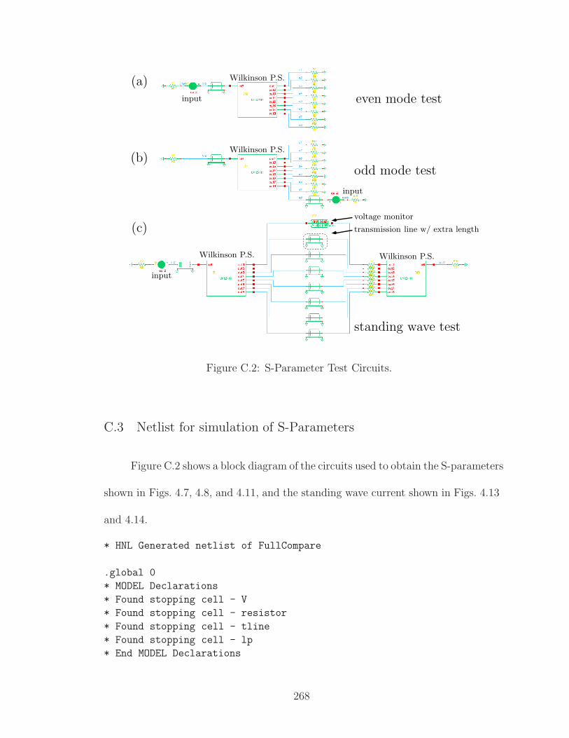
(a)
(c)
(b)
voltage monitor
Wilkinson P.S. Wilkinson P.S.
Wilkinson P.S.
Wilkinson P.S.
input
input
input
standing wave test
odd mode test
even mode test
transmission line w/ extra length
Figure C.2: S-Parameter Test Circuits.
C.3 Netlist for simulation of S-Parameters
Figure C.2 shows a block diagram of the circuits used to obtain the S-parameters
shown in Figs. 4.7, 4.8, and 4.11, and the standing wave current shown in Figs. 4.13
and 4.14.
* HNL Generated netlist of FullCompare
.global 0
* MODEL Declarations
* Found stopping cell - V
* Found stopping cell - resistor
* Found stopping cell - tline
* Found stopping cell - lp
* End MODEL Declarations
268

.subckt voltagetmonitor in0 out0
L0 vl1 net028 1p
L4 vl5 net5 1p
L1 vl2 net032 1p
L2 vl3 net036 1p
L3 vl4 net015 1p
L5 vl6 net048 1p
L6 vl7 net052 1p
L7 vl8 net056 1p
L8 vl9 net07 1p
L9 net04 out0 1p
T8 net056 0 vl9 0 Z0=32 td=11p
T9 net07 0 net04 0 Z0=32 td=11p
T4 net015 0 vl5 0 Z0=32 td=11p
T5 net5 0 vl6 0 Z0=32 td=11p
T7 net052 0 vl8 0 Z0=32 td=11p
T6 net048 0 vl7 0 Z0=32 td=11p
T2 net032 0 vl3 0 Z0=32 td=11p
T3 net036 0 vl4 0 Z0=32 td=11p
T1 net028 0 vl2 0 Z0=32 td=11p
T0 in0 0 vl1 0 Z0=32 td=11p
.ends voltagetmonitor
.subckt unit3111 in0 out1 out2 out3 out4 out5 out6 out7 out8
T9 net77 0 out1 0 Z0=33.36 td=25p
T11 net57 0 out3 0 Z0=33.36 td=25p
T13 net73 0 out5 0 Z0=33.36 td=25p
T15 net53 0 out7 0 Z0=33.36 td=25p
T16 net53 0 out8 0 Z0=33.36 td=25p
T14 net73 0 out6 0 Z0=33.36 td=25p
T12 net57 0 out4 0 Z0=33.36 td=25p
T10 net77 0 out2 0 Z0=33.36 td=25p
T4 net69 0 net45 0 Z0=19.36 td=25p
T3 net69 0 net49 0 Z0=19.36 td=25p
T8 net45 0 net53 0 Z0=21.44 td=25p
T6 net49 0 net57 0 Z0=21.44 td=25p
T0 in0 0 net61 0 Z0=47.94 td=25p
T1 net61 0 net65 0 Z0=37.24 td=25p
T2 net65 0 net69 0 Z0=20.72 td=25p
T7 net45 0 net73 0 Z0=21.44 td=25p
T5 net49 0 net77 0 Z0=21.44 td=25p
R24 0 out8 5G
R17 0 out1 5G
R18 0 out2 5G
R19 0 out3 5G
269
R21 0 out5 5G
R20 0 out4 5G
R22 0 out6 5G
R23 0 out7 5G
R13 out2 out1 58.62
R14 out4 out3 58.62
R16 out8 out7 58.62
R15 out6 out5 58.62
R6 net45 net49 23.56
R11 net57 net77 20.62
R12 net53 net73 20.62
R0 0 in0 5G
R1 0 net61 5G
R2 0 net65 5G
R3 0 net69 5G
R4 0 net49 5G
R8 0 net57 5G
R7 0 net77 5G
R10 0 net53 5G
R9 0 net73 5G
R5 0 net45 5G
.ends unit3111
XI13 net0108 net073 voltagetmonitor
T7 net0104 0 net072 0 Z0=32 td=90p
T8 net064 0 net070 0 Z0=32 td=90p
T10 net068 0 net080 0 Z0=32 td=90p
T9 net0102 0 net065 0 Z0=32 td=90p
T5 net076 0 net088 0 Z0=32 td=90p
T6 net0105 0 net092 0 Z0=32 td=90p
T4 net084 0 net096 0 Z0=32 td=90p
T3 a8 0 net055 0 Z0=50 td=250p
T0 inc 0 net059 0 Z0=50 td=250p
T2 ina 0 net095 0 Z0=50 td=250p
T1 ins 0 net043 0 Z0=50 td=250p
XI45 outc net0208 net087 net079 net083 net063 net067 net075 net071 unit3111
XI5 net059 net0108 net084 net076 net0105 net0104 net064 net0102 net068 unit3111
XI11 net095 a1 a2 a3 a4 a5 a6 a7 a8 unit3111
XI10 net043 s1 s2 s3 s4 s5 s6 s7 s8 unit3111
V2 net055 outa ac 2
V0 inc net0136 ac 2
V1 ins sin0 ac 2
R19 0 outc 50
R53 net063 net072 1n
R52 net0208 net073 1n
270
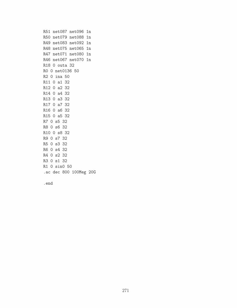
R51 net087 net096 1n
R50 net079 net088 1n
R49 net083 net092 1n
R48 net075 net065 1n
R47 net071 net080 1n
R46 net067 net070 1n
R18 0 outa 32
R0 0 net0136 50
R2 0 ina 50
R11 0 a1 32
R12 0 a2 32
R14 0 a4 32
R13 0 a3 32
R17 0 a7 32
R16 0 a6 32
R15 0 a5 32
R7 0 s5 32
R8 0 s6 32
R10 0 s8 32
R9 0 s7 32
R5 0 s3 32
R6 0 s4 32
R4 0 s2 32
R3 0 s1 32
R1 0 sin0 50
.ac dec 800 100Meg 20G
.end
271

Appendix D
Fitting Functions for Race Circuit Experiments
D.1 Two-Output Fitting Code
The following gnuplot code was used to perform the fit of the Experiment 1
data to the predictions. Comments in the code explain the details.
## This file performs the plotting of data from Experiment 2
## First do some graphical stuff
reset
set sample 300
## define a convenient rounding function
round(x) = \
(floor(x*10**(4-floor(log10(x))-1)))*1.0/10**(4-floor(log10(x))-1)
## correction term for asymmetric attenuation in experiment
zz = 3.35
## adjusting for zero phase
zot = 5.1
ll = 0
## adjusting for zero phase refence
offset1 = zot/2
offset2 = zot/2
offset3 = zot/2
offset4 = zot/2
## Correction factors from Chapter 3
a1(x) = -0.029*x+1.1214
a2(x) = 0.0147*x+0.9798
a3(x) = -0.5305*x+6.52333
## graphical options
unset key
set samples 600
## Define physical constants
272

Phi0 = 2.07/1000
ICRN = 0.75
nn = 40
t0 = 3*nn*Phi0/(2*pi*ICRN)
## define frequencies and delta values
f1 = 1.0
f2 = 1.5
f3 = 2.0
f4 = 2.5
dltA1 = 2*pi*f1*t0
dltA2 = 2*pi*f2*t0
dltA3 = 2*pi*f3*t0
dltA4 = 2*pi*f4*t0
# upside down predictions
amp1(x) = dltA1/(1+cos(a2(f1)*x))
amp2(x) = dltA2/(1+cos(a2(f2)*x))
amp3(x) = dltA3/(1+cos(a2(f3)*x))
amp4(x) = dltA4/(1+cos(a2(f4)*x))
## fit data to curves
fit [ll:pi] amp1(x+zx1)+zy1 \
"dat_andout_10.csv" u ($1-offset1):(1.0*10**(-($3-$2)/20.0*zz))\
via zx1, zy1
fit [ll:pi] amp2(x+zx2)+zy2 \
"dat_andout_15.csv" u ($1-offset2):(1.0*10**(-($3-$2)/20.0*zz))\
via zx2, zy2
fit [ll:pi] amp3(x+zx3)+zy3 \
"dat_andout_20.csv" u ($1-offset3):(1.0*10**(-($3-$2)/20.0*zz))\
via zx3, zy3
fit [ll:pi] amp4(x+zx4)+zy4 \
"dat_andout_25b.csv" u ($1-offset4):(1.0*10**(-($3-$2)/20.0*zz))\
via zx4, zy4
## record results
set print "and_out.tex"
print " & $\\theta_0$ & $A_0$ \\\\ \\hline"
print f1, " \& ", round(zx1), " \& ", round(zy1), "\\\\"
print f2, " \& ", round(zx2), " \& ", round(zy2), "\\\\"
print f3, " \& ", round(zx3), " \& ", round(zy3), "\\\\"
print f4, " \& ", round(zx4), " \& ", round(zy4), "\\\\"
## graphical options
set xrange [ll:2.5]
273

set yrange [0:1]
set xlabel "Phase (rad)"
set ylabel "Current ($I_b / I_c$)"
PNTP = 1
LNTP = 2
set label "1.0 GHz" at 1, amp1(1)-0.025
set label "1.5 GHz" at 1, amp2(1)-0.025
set label "2.0 GHz" at 1, amp3(1)-0.025
set label "2.5 GHz" at 1, amp4(1)-0.025
plot \
"dat_andout_10.csv" u \
($1-offset1):((1.0*10**(-($3-$2)/20.0*zz))):\
((1.0*10**(-($3-$2)/20.0*zz)))*log(10)/100 \
w yerrorbars pt PNTP ps 2 lt 2 lc 1, \
"dat_andout_15.csv" u \
($1-offset2):((1.0*10**(-($3-$2)/20.0*zz))):\
((1.0*10**(-($3-$2)/20.0*zz)))*log(10)/100 \
w yerrorbars pt PNTP ps 2 lt 2 lc 2, \
"dat_andout_20.csv" u \
($1-offset3):((1.0*10**(-($3-$2)/20.0*zz))):\
((1.0*10**(-($3-$2)/20.0*zz)))*log(10)/100 \
w yerrorbars pt PNTP ps 2 lt 2 lc 3, \
"dat_andout_25b.csv" u \
($1-offset4):((1.0*10**(-($3-$2)/20.0*zz))):\
((1.0*10**(-($3-$2)/20.0*zz)))*log(10)/100 \
w yerrorbars pt PNTP ps 2 lt 2 lc 4, \
amp1(x) w l lt 1 lw 2 lc 1, \
amp2(x) w l lt 1 lw 2 lc 2, \
amp3(x) w l lt 1 lw 2 lc 3, \
amp4(x) w l lt 1 lw 2 lc 4, \
amp1(x+zx1)+zy1 w l lt LNTP lc 1, \
amp2(x+zx2)+zy2 w l lt LNTP lc 2, \
amp3(x+zx3)+zy3 w l lt LNTP lc 3, \
amp4(x+zx4)+zy4 w l lt LNTP lc 4
plot \
"dat_andout_10.csv" u \
($1-offset1):((1.0*10**(-($3-$2)/20.0*zz))):\
((1.0*10**(-($3-$2)/20.0*zz)))*log(10)/100 \
w yerrorbars pt PNTP ps 2 lt 2 lc 1, \
"dat_andout_15.csv" u \
($1-offset2):((1.0*10**(-($3-$2)/20.0*zz))):\
((1.0*10**(-($3-$2)/20.0*zz)))*log(10)/100 \
w yerrorbars pt PNTP ps 2 lt 2 lc 2, \
274

"dat_andout_20.csv" u \
($1-offset3):((1.0*10**(-($3-$2)/20.0*zz))):\
((1.0*10**(-($3-$2)/20.0*zz)))*log(10)/100 \
w yerrorbars pt PNTP ps 2 lt 2 lc 3, \
"dat_andout_25b.csv" u \
($1-offset4):((1.0*10**(-($3-$2)/20.0*zz))):\
((1.0*10**(-($3-$2)/20.0*zz)))*log(10)/100 \
w yerrorbars pt PNTP ps 2 lt 2 lc 4, \
amp1(x) w l lt 1 lw 2 lc 1, \
amp2(x) w l lt 1 lw 2 lc 2, \
amp3(x) w l lt 1 lw 2 lc 3, \
amp4(x) w l lt 1 lw 2 lc 4
set term epslatex color
set output "fig_andout.tex"
replot
unset label
set label "1.0 GHz" at 1, amp1(1+zx1)-0.025+zy1
set label "1.5 GHz" at 1, amp2(1+zx2)-0.025+zy2
set label "2.0 GHz" at 1, amp3(1+zx3)-0.025+zy3
set label "2.5 GHz" at 1, amp4(1+zx4)-0.025+zy4
set output "fig_andout_detail.tex"
plot \
"dat_andout_10.csv" u \
($1-offset1):((1.0*10**(-($3-$2)/20.0*zz))):\
((1.0*10**(-($3-$2)/20.0*zz)))*log(10)/100 \
w yerrorbars pt PNTP ps 2 lt 2 lc 1, \
"dat_andout_15.csv" u \
($1-offset2):((1.0*10**(-($3-$2)/20.0*zz))):\
((1.0*10**(-($3-$2)/20.0*zz)))*log(10)/100 \
w yerrorbars pt PNTP ps 2 lt 2 lc 2, \
"dat_andout_20.csv" u \
($1-offset3):((1.0*10**(-($3-$2)/20.0*zz))):\
((1.0*10**(-($3-$2)/20.0*zz)))*log(10)/100 \
w yerrorbars pt PNTP ps 2 lt 2 lc 3, \
"dat_andout_25b.csv" u \
($1-offset4):((1.0*10**(-($3-$2)/20.0*zz))):\
((1.0*10**(-($3-$2)/20.0*zz)))*log(10)/100 \
w yerrorbars pt PNTP ps 2 lt 2 lc 4, \
amp1(x+zx1)+zy1 w l lt LNTP lc 1, \
amp2(x+zx2)+zy2 w l lt LNTP lc 2, \
amp3(x+zx3)+zy3 w l lt LNTP lc 3, \
amp4(x+zx4)+zy4 w l lt LNTP lc 4
set term x11
275

system "epstopdf fig_andout.eps"
system "epstopdf fig_andout_detail.eps"
D.2 Fit to Experiment 2 Data
Unlike the results of Experiment 1, in Chapter 5, Experiment 2 was not fit to
the expected results. Figure D.1 shows an alternative to Fig. 5.9. Figure 5.9 plotted
the measured minimum bias current as a function of input phase and showed the
predictions based on (5.3c). Here, I use the same data but allow the curve to be fit
to the data. The dashed lines are fits made to the points of the equation
Alim =2πfNt0
1 + cos(θ + θ)+ A, (D.1)
where θ and A are translation parameters which do not alter the shape of the func-
tion. The parameters θ and A allowed for shifting in amplitude, and phase. The
values are shown in Table D.1. Phase was again unknown but quantifiable. Am-
plitude was known to within errors, assuming full symmetry of the circuit from the
clock splitter onward. With this fit the same general behavior is persevered. There
is a tradeoff in comparison with the unfitted predictions. Though the lower current
amplitude limit is now closer to expectations, the phase limit predictions no longer
match as closely. This alternative analysis indicates that while the intermediate
behavior may not follow predictions closely, limits on phase and clock amplitude are
reliable.
276

0
0.2
0.4
0.6
0.8
1
0 0.5 1 1.5 2 2.5
Current(I
b/I
c)
Phase θ (rad)
1.0 GHz
1.5 GHz
2.0 GHz
2.5 GHz
Figure D.1: Curve fitting to Experiment 2. Minimum clock amplitude Ibplotted as a function of input phase θ. The original analysis of Experi-ment 2 shows the same data without fitted curves. This figure shows theresults of fitting the predicted curves to the data by translation alongthe axes.
Table D.1: Fitting parameters of and-output circuit data. θ and A areas defined in (D.1); they are a shift in the reference point of the startof the clock phase and the critical current Ic, respectively. An alternatefitting of the data from Experiment 2 to the data shifts the curves byonly small amounts, except for the highest frequency, 2.5 GHz. The datarecorded for 2.5 GHz does not follow the predicted qualitative.
f [GHz] θ A
1.0 -0.03085 -0.055381.5 -0.03194 -0.012552.0 -0.2251 0.08412.5 -0.8992 0.2677
D.3 And-Output Fitting Code for gnuplot
## This code generates the plots displaying information
277

## from the and-output race circuit experiment.
## First take care of some graphical stuff.
reset
set key bottom left
set samples 600
unset key
set format y ""
set arrow from 0.5, 100 to 0.4,100 lt -1 nohead
set arrow from 0.5, 120 to 0.4,120 lt -1 nohead
set arrow from 0.5, 100 to 0.5,120 lt -1 nohead
set label at 0.6, 110 "20 ps"
set xlabel "$\\theta$ [rad]"
set ylabel "$\\Delta t$ [ps]"
## This defines a convenient rounding function. It is cosmetic only.
round(x) = 1e-4*floor(x*1e4)
## Here I define some important physical quantities.
Phi0 = 2.07 # Magnetic flux quantum
d0 = pi*1*Phi0/0.75/0.7/1000 # values of delta
d8 = 8*d0
d20= 20*d0
## Start the fitting parameters for the RED curve
## at the values for the BLUE curve.
## 0.5 GHz
g1 = -2.1259
g2 = 48.1487
g3 = 0.1913
g4 = 1.0187
## 1.0 GHz
k1 = -2.4101
k2 = 67.2539
k3 = 1.4976
k4 = 1.2733
## 1.5 GHz
l1 = -2.5474
l2 = 49.672
l3 = 0.1178
l4 = 0.4804
## record original values for comparison
Ag1 = g1
278

Ag2 = g2
Ag3 = g3
Ag4 = g4
Ak1 = k1
Ak2 = k2
Ak3 = k3
Ak4 = k4
Al1 = l1
Al2 = l2
Al3 = l3
Al4 = l4
## Here I define the delay functions (RED curve)
n0(x) = g4*(acos(cos(x) - d0) - x)/(2*pi/1000)
n8(x) = g4*(acos(cos(x) - g3*d8) - x)/(2*pi/1000)
n20(x)= g4*(acos(cos(x) - g3*d20) - x)/(2*pi/1000)
m0(x) = k4*(acos(cos(x) - d0*0.5) - x)/(2*pi/500)
m8(x) = k4*(acos(cos(x) - k3*d8*0.5) - x)/(2*pi/500)
m20(x)= k4*(acos(cos(x) - k3*d20*0.5) - x)/(2*pi/500)
h0(x) = l4*(acos(cos(x) - d0*1.5) - x)/(2*pi/1500)
h8(x) = l4*(acos(cos(x) - l3*d8*1.5) - x)/(2*pi/1500)
h20(x)= l4*(acos(cos(x) - l3*d20*1.5) - x)/(2*pi/1500)
## Here I define the delay functions (BLUE curve)
An0(x) = Ag4*(acos(cos(x) - d0) - x)/(2*pi/1000)
An8(x) = Ag4*(acos(cos(x) - Ag3*d8) - x)/(2*pi/1000)
An20(x)= Ag4*(acos(cos(x) - Ag3*d20) - x)/(2*pi/1000)
Am0(x) = Ak4*(acos(cos(x) - d0*0.5) - x)/(2*pi/500)
Am8(x) = Ak4*(acos(cos(x) - Ak3*d8*0.5) - x)/(2*pi/500)
Am20(x)= Ak4*(acos(cos(x) - Ak3*d20*0.5) - x)/(2*pi/500)
Ah0(x) = Al4*(acos(cos(x) - d0*1.5) - x)/(2*pi/1500)
Ah8(x) = Al4*(acos(cos(x) - Al3*d8*1.5) - x)/(2*pi/1500)
Ah20(x)= Al4*(acos(cos(x) - Al3*d20*1.5) - x)/(2*pi/1500)
## This fit finds the middle starting port for the red curve fit.
fit n20(x+g1)-n8(x+g1)+g2 "dat_twoout.dat" u 1:2:3 via g1
fit m20(x+k1)-m8(x+k1)+k2 "dat_twoout2.dat" u 1:2:3 via k1
fit h20(x+l1)-h8(x+l1)+l2 "dat_twoout3.dat" u 1:2:3 via l1
279
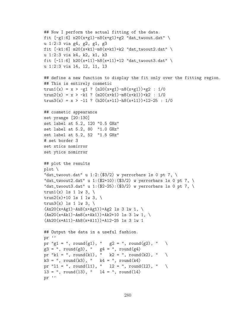
## Now I perform the actual fitting of the data.
fit [-g1:6] n20(x+g1)-n8(x+g1)+g2 "dat_twoout.dat" \
u 1:2:3 via g4, g2, g1, g3
fit [-k1:6] m20(x+k1)-m8(x+k1)+k2 "dat_twoout2.dat" \
u 1:2:3 via k4, k2, k1, k3
fit [-l1:6] h20(x+l1)-h8(x+l1)+l2 "dat_twoout3.dat" \
u 1:2:3 via l4, l2, l1, l3
## define a new function to display the fit only over the fitting region.
## This is entirely cosmetic
trun1(x) = x > -g1 ? (n20(x+g1)-n8(x+g1))+g2 : 1/0
trun2(x) = x > -k1 ? (m20(x+k1)-m8(x+k1))+k2 : 1/0
trun3(x) = x > -l1 ? (h20(x+l1)-h8(x+l1))+l2-25 : 1/0
## cosmetic appearance
set yrange [20:130]
set label at 5.2, 120 "0.5 GHz"
set label at 5.2, 80 "1.0 GHz"
set label at 5.2, 52 "1.5 GHz"
# set border 3
set xtics nomirror
set ytics nomirror
## plot the results
plot \
"dat_twoout.dat" u 1:2:($3/2) w yerrorbars ls 0 pt 7, \
"dat_twoout2.dat" u 1:($2+10):($3/2) w yerrorbars ls 0 pt 7, \
"dat_twoout3.dat" u 1:($2-25):($3/2) w yerrorbars ls 0 pt 7, \
trun1(x) ls 1 lw 3, \
trun2(x)+10 ls 1 lw 3, \
trun3(x) ls 1 lw 3, \
(An20(x+Ag1)-An8(x+Ag1))+Ag2 ls 3 lw 1, \
(Am20(x+Ak1)-Am8(x+Ak1))+Ak2+10 ls 3 lw 1, \
(Ah20(x+Al1)-Ah8(x+Al1))+Al2-25 ls 3 lw 1
## Output the data in a useful fashion.
pr ’’
pr "g1 = ", round(g1), " g2 = ", round(g2), " \
g3 = ", round(g3), " g4 = ", round(g4)
pr "k1 = ", round(k1), " k2 = ", round(k2), " \
k3 = ", round(k3), " k4 = ", round(k4)
pr "l1 = ", round(l1), " l2 = ", round(l2), " \
l3 = ", round(l3), " l4 = ", round(l4)
pr ’’
280

set print "two_out.tex"
pr " & & 0.5 GHz & 1.0 GHz & 1.5 GHz \\\\ \\hline"
pr "\\multirow4*Red Fit & $\\gamma_1$ & ", \
round(1.0/g3), " & ", round(1.0/k3), " & ", \
round(1.0/l3), " \\\\"
pr " & $\\gamma_2$ & ", round(g1), " &", round(k1), \
" & ", round(l1), " \\\\"
pr " & $\\gamma_3$ & ", round(g2), " & ", round(k2), \
" & ", round(l2), " \\\\"
pr " & $\\gamma_4$ & ", round(g4/g3), " & ", \
round(k4/k3), " & ", round(l4/l3), " \\\\ \\hline"
pr "\\multirow4*Blue Fit & $\\gamma_1$ & ", \
round(1.0/Ag3), " & ", round(1.0/Ak3), " & ", \
round(1.0/Al3), " \\\\"
pr " & $\\gamma_2$ & ", round(Ag1), " &", round(Ak1), \
" & ", round(Al1), " \\\\"
pr " & $\\gamma_3$ & ", round(Ag2), " & ", round(Ak2), \
" & ", round(Al2), " \\\\"
pr " & $\\gamma_4$ & ", round(Ag4/Ag3), " & ", \
round(Ak4/Ak3), " & ", round(Al4/Al3), " \\\\ \\hline"
# set xrange [0:2*pi]
set term epslatex color
set output "fig_twoexp.tex"
replot
set term x11
system "epstopdf fig_twoexp.eps"
set term epslatex color standalone
set output "fig_twoexp_sa.tex"
replot
set term x11
set print ’-’
pr "latex fig_twoexp_sa.tex; dvips fig_twoexp_sa; \
epstopdf fig_twoexp_sa.ps"
281

D.4 Calculation of Depressed IcRN Product
Experiment 2 in Chapter 5 indicated that at a known calibration point, Ib = Ic,
the measurement of the bias current through the junctions could confirm the power
delivered to the chip. Results matched expectations, given that attenuators in the
test setup are accurate only to approximately 10%. This reference was subsequently
used in calculations for Experiment 3. When adjusted using this calibration, the
measured IcRN product of the experimental chip was 0.770 mV.
Alternatively, I can try ignoring this correction and proceed with the calcu-
lations. The results are shown in Table D.2. In this case, the average value of the
timing parameter t0 is 0.77 ps and the average value of IcRN is 0.44 mV. Just as
importantly, as frequency increases the lower bias current limit increases to close to
A = 1, which one would expect close to the highest operating frequency. Assuming
a depression of the IcRN product by almost one-half, the maximum frequency of the
circuits in the experiment would decrease by the same factor. This fits observations
that the maximum operating frequency of the experiments was 2.5 GHz, despite a
design for a maximum frequency of 5 GHz.
While the IcRN product is generally constant for a given process, it can ef-
fectively be changed by a different βc value. The βc value is determined both by
design and fabrication. The value of the shunt resistor RN can be chosen to essen-
tially scale the IcRN product and change the switching time of junctions. However,
misalignment during the fabrication process can change the resistor values from the
design, thus slowing down the junctions. A test of the chip fabrication properties
282
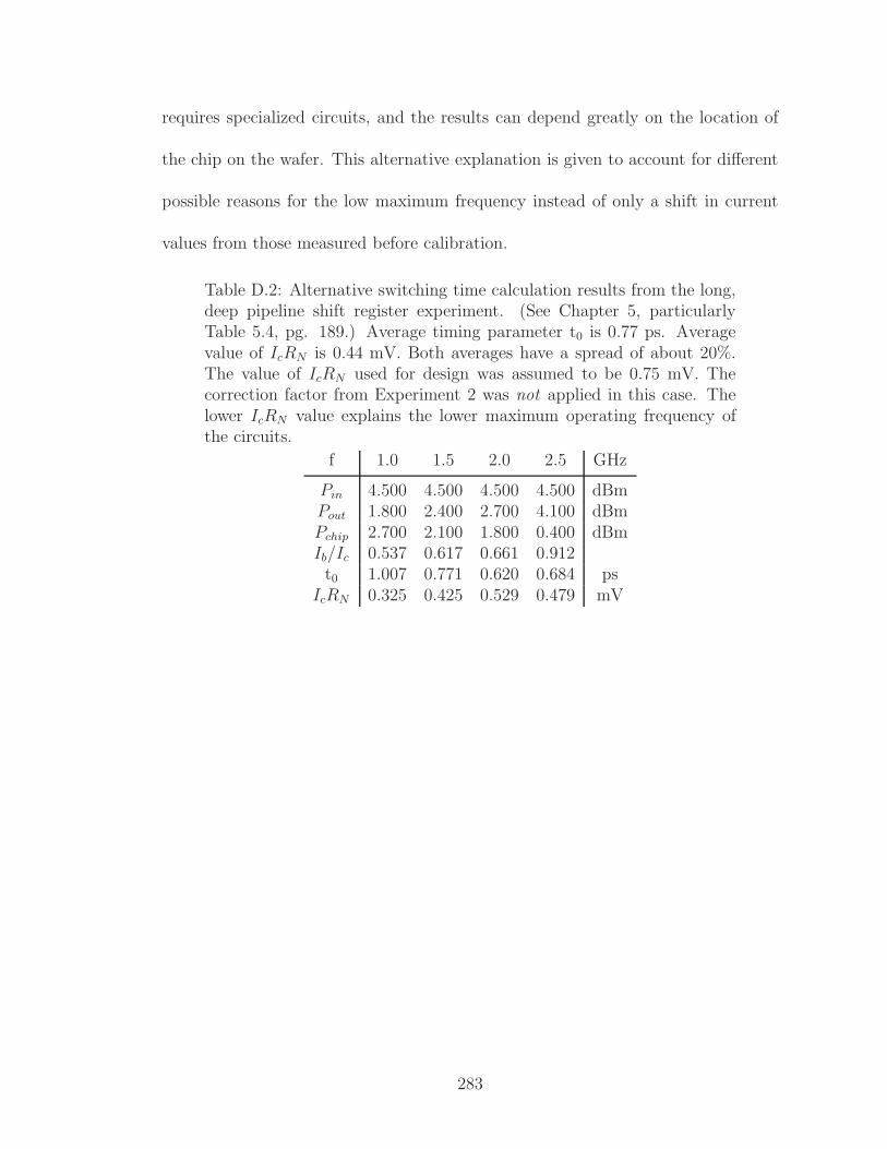
requires specialized circuits, and the results can depend greatly on the location of
the chip on the wafer. This alternative explanation is given to account for different
possible reasons for the low maximum frequency instead of only a shift in current
values from those measured before calibration.
Table D.2: Alternative switching time calculation results from the long,deep pipeline shift register experiment. (See Chapter 5, particularlyTable 5.4, pg. 189.) Average timing parameter t0 is 0.77 ps. Averagevalue of IcRN is 0.44 mV. Both averages have a spread of about 20%.The value of IcRN used for design was assumed to be 0.75 mV. Thecorrection factor from Experiment 2 was not applied in this case. Thelower IcRN value explains the lower maximum operating frequency ofthe circuits.
f 1.0 1.5 2.0 2.5 GHz
Pin 4.500 4.500 4.500 4.500 dBmPout 1.800 2.400 2.700 4.100 dBmPchip 2.700 2.100 1.800 0.400 dBmIb/Ic 0.537 0.617 0.661 0.912t0 1.007 0.771 0.620 0.684 ps
IcRN 0.325 0.425 0.529 0.479 mV
283

Appendix E
Hypres Fabrication Summary
The experiments described in this thesis were performed on chips manufac-
tured by Hypres, Inc. This appendix briefly summarizes the design rules for this
process. The Hypres niobium integrated circuit fabrication design rules are avail-
able on the Hypres website [29]. The designs described here follow the 24th revision,
dated January 11, 2008.
Niobium is the superconducting material in the Hypres integrated circuits.
The junctions are Niobium/Aluminum-Oxide/Niobium SIS Josephson junctions fab-
ricated using an in-situ trilayer over the entire wafer. Junction areas are created
through photolithography and etching of the trilayer. The photolithography does
not employ any size reduction. All my integrated circuits used the 4.5 kA/cm2
critical current density process. There are four superconducting niobium metal lay-
ers. Josephson junctions are connected between the second and third metallization
layers. Junctions are shunted by normal metal in a separate molybdenum normal
metal layer. The molybdenum layer has a sheet resistance of 2.1± 0.3Ω per square.
The metal layers are insulated with silicon dioxide. Josephson junctions are addi-
tionally insulated by anodization of the base electrode of the trilayer. The specific
capacitance of junctions is approximately 59 fF/µm2 for the 4.5kA/cm2 process.
Fabrication is done on 6-inch (150 mm) diameter oxidized silicon wafers. The
284

Hypres design rules specify a number of constraints on design of integrated circuits
and the accuracy of circuit elements in fabrication. These can be found in the
published design rules. The physical design of integrated circuits is shown in Table
E.1. This includes 11 process layers, a minimum feature size of 1µm, and current
density tolerance and resistor tolerances of ±5% on chip and ±15% between runs.
The maximum microstrip impedance using this process is 42Ω, using M0 as
the signal layer, M3 as the ground plane. In this case, the width of the microstrip
is 2.5µm and the spacing between the M0 signal and M0 ground is 2.5µm. Due to
fabrication bias of −0.2µm, the actual fabricated width of the microstrip is about
2.3µm wide.
285
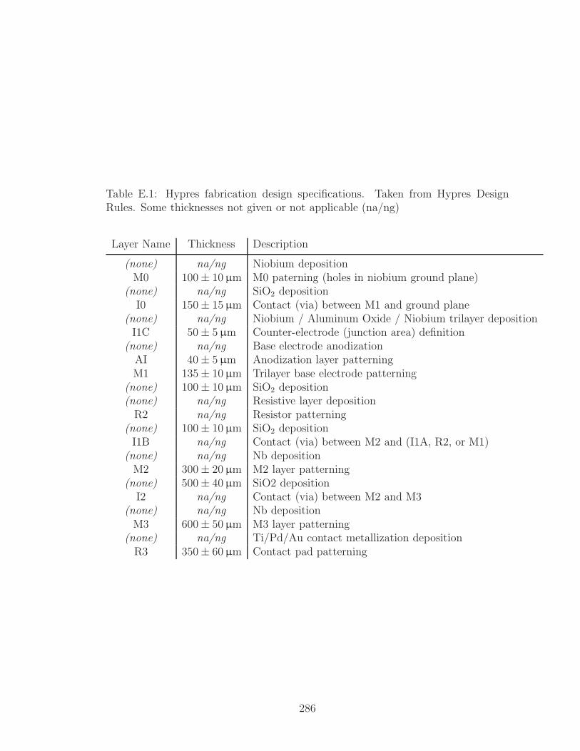
Table E.1: Hypres fabrication design specifications. Taken from Hypres DesignRules. Some thicknesses not given or not applicable (na/ng)
Layer Name Thickness Description
(none) na/ng Niobium depositionM0 100± 10µm M0 paterning (holes in niobium ground plane)
(none) na/ng SiO2 depositionI0 150± 15µm Contact (via) between M1 and ground plane
(none) na/ng Niobium / Aluminum Oxide / Niobium trilayer depositionI1C 50± 5µm Counter-electrode (junction area) definition
(none) na/ng Base electrode anodizationAI 40± 5µm Anodization layer patterningM1 135± 10µm Trilayer base electrode patterning
(none) 100± 10µm SiO2 deposition(none) na/ng Resistive layer depositionR2 na/ng Resistor patterning
(none) 100± 10µm SiO2 depositionI1B na/ng Contact (via) between M2 and (I1A, R2, or M1)
(none) na/ng Nb depositionM2 300± 20µm M2 layer patterning
(none) 500± 40µm SiO2 depositionI2 na/ng Contact (via) between M2 and M3
(none) na/ng Nb depositionM3 600± 50µm M3 layer patterning
(none) na/ng Ti/Pd/Au contact metallization depositionR3 350± 60µm Contact pad patterning
286
Appendix F
Spice Netlist of CLA* HNL Generated netlist of AN_chip21
.global 0
* MODEL Declarations
* Found stopping cell - lm_open
* Found stopping cell - junction
* Found stopping cell - muind
* Found stopping cell - rsj
.subckt rsj a b jjmod=jj110D ic=0.25 icrn=0.7 rsh=2.8 lprsh=1.5p
b0 a b phi jjmod area=ic
r_sh a a1 rsh
lp_rsh a1 b lprsh
.ends rsj
* Found stopping cell - lp
* Found stopping cell - inductor
* Found stopping cell - resistor
* End MODEL Declarations
.subckt on_input_wireup ci1 ci2 ci3 ci4 ci5 ci6 ci7 ci8 cq1 cq2 cq3
cq4 cq5 cq6 cq7 cq8 wi1 wi2 wi3 wi4 wi5 wi6 wi7 wi8
wq1 wq2 wq3 wq4 wq5 wq6 wq7 wq8
L15 wq1 cq1 1p
L14 wq2 cq2 1p
L13 wq3 cq3 1p
L12 wq4 cq4 1p
L11 wq5 cq5 1p
L10 wq6 cq6 1p
L9 wq7 cq7 1p
L8 wq8 cq8 1p
L7 wi8 ci8 1p
L6 wi7 ci7 1p
L5 wi6 ci6 1p
L4 wi5 ci5 1p
L3 wi4 ci4 1p
L2 wi3 ci3 1p
L1 wi2 ci2 1p
287
L0 wi1 ci1 1p
.ends on_input_wireup
.subckt on_output_wireup ci1 ci2 ci3 ci4 ci5 ci6 ci7 ci8 cq1 cq2 cq3
cq4 cq5 cq6 cq7 cq8 wi1 wi2 wi3 wi4 wi5 wi6 wi7 wi8 wq1 wq2 wq3 wq4
wq5 wq6 wq7 wq8
L15 wq1 cq1 1p
L14 wq2 cq2 1p
L13 wq3 cq3 1p
L12 wq4 cq4 1p
L11 wq5 cq5 1p
L10 wq6 cq6 1p
L9 wq7 cq7 1p
L8 wq8 cq8 1p
L7 wi8 ci8 1p
L6 wi7 ci7 1p
L5 wi6 ci6 1p
L4 wi5 ci5 1p
L3 wi4 ci4 1p
L2 wi3 ci3 1p
L1 wi2 ci2 1p
L0 wi1 ci1 1p
.ends on_output_wireup
.subckt on_50_ohm_wps_40pin p1 p2 p3 p4 p5 p6 p7 p8 uwin
R6 net49 net11 23.56
R5 net47 net13 20.62
R4 net43 net15 20.62
R3 p8 p7 58.62
R2 p6 p5 58.62
R1 p4 p3 58.62
R0 p2 p1 58.62
L16 net47 p8 1p
L15 net47 p7 1p
L14 net13 p6 1p
L13 net13 p5 1p
L12 net43 p4 1p
L11 net43 p3 1p
L10 net15 p2 1p
L9 net15 p1 1p
L8 net11 net15 1p
L7 net11 net43 1p
L6 net49 net13 1p
L5 net49 net47 1p
288

L4 net53 net49 1p
L3 net53 net11 1p
L0 uwin net53 1p
.ends on_50_ohm_wps_40pin
.subckt n_bias_out bias c0 c1 d0 d1
c0 c0 0 5.28f
K1 L1 L0 0.936529
K1d L1d L0 0.218218
L0 0 bias 1p
L1 c1 c0 13.18p
L1d d1 d0 5.25p
.ends n_bias_out
.subckt m_out_rql a b c c00 c01 c10 c11 dc0 dc1
L0 net72 net33 12.6p
L6 net41 net72 750f
L9 net57 net59 1.5p
Lf c10 c00 1f
L10 net59 net38 9.2p
L5 net61 b 962f
L4 net61 net59 962f
L3 net68 net59 750f
L2 a net68 750f
L8 net57 net70 2.56p
L7 net70 net72 1.05p
Lp0 net39 0 200f
Lc net41 c 2f
Lp4 net43 0 200f
Lp2 net45 0 200f
Lp3 net47 0 200f
Lp1 net49 0 200f
Xb2 net45 net57 rsj jjmod=Hyp5a ic=0.200 icrn=0.7 rsh=3.5 lprsh = 1.75p
Xb0 net39 net41 rsj jjmod=Hyp5a ic=0.400 icrn=0.35 rsh=875.000m lprsh = 437.5f
Xb4 net43 net61 rsj jjmod=Hyp5a ic=0.312 icrn=0.7 rsh=2.24359 lprsh = 1.121795p
Xb3 net47 net68 rsj jjmod=Hyp5a ic=0.400 icrn=0.7 rsh=1.75 lprsh = 875.000f
Xb1 net49 net70 rsj jjmod=Hyp5a ic=0.282 icrn=0.7 rsh=2.48227 lprsh = 1.241135p
XI14 net33 c11 net34 dc0 net37 n_bias_out
XI13 net38 net34 c01 net37 dc1 n_bias_out
.ends m_out_rql
.subckt m_out_squid a b c
c0 g 0 44f
c1 h 0 16f
c2 f 0 16f
289
c3 c f 5f
c4 d h 5f
c5 e bb 10f
K0 L0 L1 0.64
K1 L2 L3 0.64
Xb1 f g rsj jjmod=Hyp5a ic=0.168 icrn=0.42 rsh=2.5 lprsh = 1.25p
b0 h g phib0 Hyp5a area=0.168
L6 b bb 120p
L5 g a 120p
L7 c d 200f
L2 bb h 3.92p
L3 d e 5.17p
L1 e 0 5.17p
L0 f bb 3.92p
.ends m_out_squid
.subckt m_out12 a c00 c01 c10 c11 dc0 dc1 q
R1 net23 0 50
R0 0 net28 50
XI11 net77 net23 net33 net021 net022 c10 c11 dc0 net019 m_out_rql
XI10 net84 net77 net36 net030 net031 net021 net022 net019 net028 m_out_rql
XI9 net91 net84 net39 net033 net040 net030 net031 net028 net037 m_out_rql
XI8 net98 net91 net42 net042 net049 net033 net040 net037 net046 m_out_rql
XI7 net105 net98 net97 net051 net050 net042 net049 net046 net045 m_out_rql
XI6 net112 net105 net104 net066 net067 net051 net050 net045 net064 m_out_rql
XI5 net119 net112 net51 net069 net076 net066 net067 net064 net073 m_out_rql
XI4 net126 net119 net118 net078 net085 net069 net076 net073 net082 m_out_rql
XI3 net133 net126 net125 net087 net094 net078 net085 net082 net091 m_out_rql
XI2 net140 net133 net132 net096 net0103 net087 net094 net091 net0100 m_out_rql
XI1 net147 net140 net139 net0111 net0112 net096 net0103 net0100 net0109
m_out_rql
XI0 a net147 net146 c00 c01 net0111 net0112 net0109 dc1 m_out_rql
XI23 q net37 net33 m_out_squid
XI22 net37 net40 net36 m_out_squid
XI21 net40 net43 net39 m_out_squid
XI20 net43 net44 net42 m_out_squid
XI19 net44 net49 net97 m_out_squid
XI18 net49 net52 net104 m_out_squid
XI17 net52 net55 net51 m_out_squid
XI16 net55 net58 net118 m_out_squid
XI15 net58 net61 net125 m_out_squid
XI14 net61 net64 net132 m_out_squid
XI13 net64 net67 net139 m_out_squid
XI12 net67 net28 net146 m_out_squid
.ends m_out12
290

.subckt n_bias bias c0 c1 d0 d1
c0 c0 0 2.64f
L0 0 bias 1p
L1 c1 c0 6.59p
L1d d1 d0 5.25p
K1 L1 L0 0.662226
K1d L1d L0 0.218218
.ends n_bias
.subckt q_out400e_v a bias q
Xb1 net010 net050 rsj jjmod=Hyp5a ic=0.400 icrn=0.75 rsh=1.875 lprsh = 937.5f
Xb2 net035 net026 rsj jjmod=Hyp5a ic=0.200 icrn=0.42 rsh=2.1 lprsh = 1.05p
LPbias1 net011 0 1f
b3 net023 net030 phib3 Hyp5a area=0.141
Lg1 net050 0 200f
Lg2 net026 0 600f
Lg3 net023 net035 100f
Lg5 net035 q 100f
Lp net010 net012 55f
L7 net030 net011 3.5p
Lbias bias net010 9.3p
L5 net012 a 1.05p
L6 net012 net030 2.5p
.ends q_out400e_v
.subckt q_out282e a bias q
Lg0 net013 0 200f
Xb0 net08 net013 rsj jjmod=Hyp5a ic=0.282 icrn=0.75 rsh=2.659574
lprsh = 1.329787p
L3 a net08 1.5p
L4 net08 q 1.5p
Lbias bias net08 13.7p
.ends q_out282e
.subckt q_in a0 a1 q
Xb0 net020 net013 rsj jjmod=Hyp5a ic=0.141 icrn=0.75 rsh=5.319149
lprsh = 2.659575p
Lb0 net020 0 170f
L1 net013 q 200f
K2 L2 L0 0.484934
L0 0 net013 12p
L2 a1 a0 93p
.ends q_in
291

.subckt q_c0_io a a0 a1 c01 c11 dc0 dc1 q qv
XI4 net14 c01 net11 net13 dc1 n_bias
XI3 net19 net11 c11 dc0 net13 n_bias
XI2 net20 net14 qv q_out400e_v
XI1 a net19 net20 q_out282e
XI0 a0 a1 q q_in
.ends q_c0_io
.subckt a_jtl_chop a bias q
Lg0 net013 0 220f
Lg1 net05 0 150f
L6 net014 q 1f
Xb1 net014 net05 rsj jjmod=Hyp5a ic=0.200 icrn=0.75 rsh=3.75 lprsh = 1.875p
Xb0 net021 net013 rsj jjmod=Hyp5a ic=0.141 icrn=0.75 rsh=5.319149
lprsh = 2.659575p
L3 a net021 3.0p
L4 net021 net019 3.0p
Lbias bias net019 13.4p
L5 net019 net014 2.1p
.ends a_jtl_chop
.subckt n_bias_ihm bias c0 c1 d0 d1
c0 c0 0 1.79f
L0 0 bias 1p
L1 c1 c0 4.47p
L1d d1 d0 3.67p
K1 L1 L0 0.402036
K1d L1d L0 0.260998
.ends n_bias_ihm
.subckt a_anotb a b d0 d1 q
cb b 0 58.71f
ca a 0 91.30f
Lp0 net19 net023 96f
Lg1 net018 0 172f
Lg0 net027 0 106f
Xb0 net023 net027 rsj jjmod=Hyp5a ic=0.141 icrn=0.75 rsh=5.319149
lprsh = 2.659575p
Xb1 net019 net018 rsj jjmod=Hyp5a ic=0.100 icrn=0.75 rsh=7.5 lprsh = 3.75p
K3 L10 L11 0.289
k05 L0 L5 0.0672226
k65 L5 L6 0.815404
L11 0 net031 1p
L10 d1 net044 1p
L3 b net019 2.1p
292

L7 net19 q 3.0p
L4 a net19 2.1p
L0 d0 net044 1p
L5 net019 0 18.355p
L6 net031 net023 19.913p
.ends a_anotb
.subckt a_jtle_chop a bias q
Lg0 net08 0 230f
Lg1 net010 0 150f
L6 net014 q 1f
Xb1 net014 net010 rsj jjmod=Hyp5a ic=0.200 icrn=0.75 rsh=3.75 lprsh = 1.875p
Xb0 net013 net08 rsj jjmod=Hyp5a ic=0.141 icrn=0.75 rsh=5.319149
lprsh = 2.659575p
L3 a net013 3.0p
L4 net013 net019 2.67p
Lbias bias net019 11.7p
L5 net019 net014 2.43p
.ends a_jtle_chop
.subckt a_or a b bias qo
L5 net10 net029 20p
L6 net10 net62 20p
L3 net050 net44 20.5p
L4 net58 net44 20.5p
L8 net51 qo 3.0p
L7 net19 net20 23.5p
L9 net059 net034 15.2p
Lbias bias net085 17.4p
Xb0 net51 net29 rsj jjmod=Hyp5a ic=0.118 icrn=0.75 rsh=6.355932
lprsh = 3.177966p
Xb1 net059 net41 rsj jjmod=Hyp5a ic=0.118 icrn=0.75 rsh=6.355932
lprsh = 3.177966p
Lp1 net20 net059 671f
Lp2 net19 net44 200f
Lp0 net19 net085 277f
Lb0 net29 0 245f
Lb1 net41 0 62f
Lp5 a net050 387f
Lp4 net51 net085 11f
Lp6 b net58 442f
Lp3 net20 net10 630f
k35 L3 L5 0.78
k46 L4 L6 0.78
LPag net034 0 1f
293

LPqq net050 net62 1f
LPq net58 net029 1f
.ends a_or
.subckt a_and a b bias qa
LPqq net030 net62 1f
LPq net026 net028 1f
L4 net026 net034 20.5p
L6 net58 net62 20p
L5 net58 net028 20p
L3 net030 net034 20.5p
L7 net19 net20 23.9p
L9 net018 qa 3.0p
Lbias bias net036 17.4p
Xb0 net036 net019 rsj jjmod=Hyp5a ic=0.128 icrn=0.375 rsh=2.929688
lprsh = 1.464844p
Xb1 net018 net049 rsj jjmod=Hyp5a ic=0.118 icrn=0.75 rsh=6.355932
lprsh = 3.177966p
Lp1 net20 net018 760f
Lp2 net19 net034 500f
Lp0 net19 net036 470f
Lg0 net019 0 170f
Lg1 net049 0 90f
Lp5 a net030 620f
Lp6 b net026 620f
Lp3 net20 net58 550f
k35 L3 L5 0.78
k46 L4 L6 0.78
.ends a_and
.subckt a_jtl_e a bias q
Lg0 net08 0 230f
Lg1 net010 0 230f
Xb1 net014 net010 rsj jjmod=Hyp5a ic=0.200 icrn=0.75 rsh=3.75 lprsh = 1.875p
Xb0 net022 net08 rsj jjmod=Hyp5a ic=0.141 icrn=0.75 rsh=5.319149
lprsh = 2.659575p
L3 a net022 3.0p
L4 net022 net019 3.3p
Lbias bias net019 11.2p
L5 net019 net014 1.8p
L6 net014 q 2.1p
.ends a_jtl_e
.subckt a_c3_b3 a b bias15 bias16 c00 c01 c10 c11 dc0 dc1 dc2 dc3 g gl gm pm1 q
L0 net070 c11 1p
294

XI47 bias16 net075 net070 net0153 net085 n_bias
XI46 bias15 c01 net075 net0148 net056 n_bias
XI5 net31 net54 net55 a_jtl_chop
XI40 net33 net0150 net0145 net085 net0148 n_bias_ihm
XI43 net25 net0100 net0120 net0103 net0123 n_bias_ihm
XI48 net0101 net097 c00 net059 dc1 n_bias
XI44 net36 c10 net0115 dc0 net0118 n_bias
XI22 net0149 net0145 net097 net056 net059 n_bias
XI38 net0134 net090 net0150 net0133 net0153 n_bias
XI26 net54 net0120 net090 net0123 net0133 n_bias
XI27 net047 net0115 net0100 net0118 net0103 n_bias
Xanotb a b dc2 dc3 net013 a_anotb
XI2 gm net0134 net22 a_jtle_chop
XI3 gl net0149 net34 a_jtle_chop
XI4 pm1 net0101 net32 a_jtle_chop
Xor net22 net55 net25 net49 a_or
Xand1 net32 net34 net33 net31 a_and
XI1 net49 net36 g a_jtl_e
XI6 net013 net047 q a_jtl_e
.ends a_c3_b3
.subckt a_jtle_ a bias q
Lg0 net013 0 230f
Lg1 net05 0 230f
Xb1 net023 net05 rsj jjmod=Hyp5a ic=0.200 icrn=0.75 rsh=3.75 lprsh = 1.875p
Xb0 net021 net013 rsj jjmod=Hyp5a ic=0.141 icrn=0.75 rsh=5.319149
lprsh = 2.659575p
L3 a net021 3.0p
L4 net021 net037 2.67p
Lbias bias net037 11.7p
L5 net037 net023 2.43p
L6 net023 q 2.1p
.ends a_jtle_
.subckt a_and011 a b bias qa
LPqq net053 net62 1f
LPq net034 net029 1f
L4 net034 net051 20.5p
L6 net58 net62 20p
L5 net58 net029 20p
L3 net053 net051 20.5p
L7 net19 net20 12.5p
L9 net018 qa 3.0p
Lbias bias net020 13.0p
Xb0 net020 net019 rsj jjmod=Hyp5a ic=0.118 icrn=0.375 rsh=3.177966
295

lprsh = 1.588983p
Xb1 net018 net063 rsj jjmod=Hyp5a ic=0.118 icrn=0.75 rsh=6.355932
lprsh = 3.177966p
Lp1 net20 net018 616f
Lp2 net19 net051 76f
Lp0 net19 net020 400f
Lg0 net019 0 275f
Lg1 net063 0 96f
Lp5 a net053 450f
Lp6 b net034 450f
Lp3 net20 net58 503f
k35 L3 L5 0.78
k46 L4 L6 0.78
.ends a_and011
.subckt a_jtl a bias q
Lg0 net013 0 230f
Lg1 net010 0 230f
Xb1 net022 net010 rsj jjmod=Hyp5a ic=0.200 icrn=0.75 rsh=3.75 lprsh = 1.875p
Xb0 net021 net013 rsj jjmod=Hyp5a ic=0.141 icrn=0.75 rsh=5.319149
lprsh = 2.659575p
L3 a net021 3.0p
L4 net021 net019 3.0p
Lbias bias net019 13.4p
L5 net019 net022 2.1p
L6 net022 q 2.1p
.ends a_jtl
.subckt a_c2_b3 a a_ b b_ bias1a bias2a bias2i bias3 bias7 c00 c01 c10
c11 dc0 dc1 g1 g1a g2 g2a g2i g3 g7 g15 g16 gl gm p1 pl pm1 pm2
L0 c00 c10 1p
XI2 net222 g2i net253 a_jtl_chop
XI40 bias2a net168 net163 net165 net170 n_bias_ihm
XI41 bias1a c01 net168 net170 dc1 n_bias_ihm
XI33 net126 net153 net123 net125 net155 n_bias_ihm
XI42 net234 net198 net133 net135 net0149 n_bias
XI43 bias7 net133 c11 dc0 net135 n_bias
XI36 net231 net183 net198 net0149 net185 n_bias
XI30 net249 net193 net183 net185 net195 n_bias
XI31 net216 net188 net153 net155 net190 n_bias
XI39 bias2i net163 net158 net160 net165 n_bias
XI38 bias3 net158 net173 net175 net160 n_bias
XI35 net181 net173 net178 net180 net175 n_bias
XI34 net191 net178 net188 net190 net180 n_bias
XI17 net196 net203 net193 net195 net205 n_bias
296
XI28 net206 net123 net203 net205 net125 n_bias
XI12 a_ net191 net211 a_jtle_
XI11 b_ net181 net214 a_jtle_
XI1 gm net216 net217 a_jtle_chop
Xor net217 net253 net126 net218 a_or
Xand1 pm1 gl g1a net222 a_and011
Xand2 pm2 pl g2a net227 a_and011
XI4 net244 net231 p1 a_jtl_e
XI8 net250 net234 g2 a_jtl_e
XI7 net250 g7 g1 a_jtl_e
XI3 net227 g3 net244 a_jtl
XI13 net214 net206 net247 a_jtl
XI5 net218 net249 net250 a_jtl
XI15 net247 g15 b a_jtl
XI16 net262 g16 a a_jtl
XI14 net211 net196 net262 a_jtl
.ends a_c2_b3
.subckt a_jtl_chop_e a bias q
Lg0 net010 0 230f
Lg1 net015 0 158f
L6 net022 q 1f
Xb1 net022 net015 rsj jjmod=Hyp5a ic=0.200 icrn=0.75 rsh=3.75 lprsh = 1.875p
Xb0 net013 net010 rsj jjmod=Hyp5a ic=0.141 icrn=0.75 rsh=5.319149
lprsh = 2.659575p
L3 a net013 3.0p
L4 net013 net019 3.3p
Lbias bias net019 11.2p
L5 net019 net022 1.8p
.ends a_jtl_chop_e
.subckt m_outjtl282_400 a bias q
Lg0 net010 0 200f
Lg1 net04 0 200f
Xb1 net023 net04 rsj jjmod=Hyp5a ic=0.400 icrn=0.75 rsh=1.875 lprsh = 937.5f
Xb0 net013 net010 rsj jjmod=Hyp5a ic=0.282 icrn=0.75 rsh=2.659574
lprsh = 1.329787p
L3 a net013 1.5p
L4 net013 net027 1.5p
Lbias bias net027 6.2p
L5 net023 net027 1.05p
L6 net023 q 1.05p
.ends m_outjtl282_400
.subckt a_andor011 a b bias qa qo
297

LPqq net060 net022 1f
LPq net62 net031 1f
L5 net58 net031 20p
L6 net58 net022 20p
L3 net060 net035 20.5p
L4 net62 net035 20.5p
L8 net055 qo 3.0p
L7 net19 net20 20.0p
L9 net066 qa 3.0p
Lbias bias net51 11.8p
Xb0 net055 net29 rsj jjmod=Hyp5a ic=0.118 icrn=0.75 rsh=6.355932
lprsh = 3.177966p
Xb1 net066 net41 rsj jjmod=Hyp5a ic=0.118 icrn=0.75 rsh=6.355932
lprsh = 3.177966p
Lp1 net20 net066 760f
Lp2 net19 net035 500f
Lp0 net19 net51 470f
Lg0 net29 0 140f
Lg1 net41 0 90f
Lp5 a net060 620f
Lp4 net055 net51 1f
Lp6 b net62 620f
Lp3 net20 net58 550f
k35 L3 L5 0.78
k46 L4 L6 0.78
.ends a_andor011
.subckt a_c5_b5 a b c00 c01 c10 c11 dc0 dc1 dc2 dc3 q
XI31 b net072 net0110 a_jtl_chop_e
XI32 a net067 net0107 a_jtl_chop_e
XI51 net067 net068 net063 net065 net070 n_bias
XI50 net072 c00 net068 net070 net0123 n_bias
XI22 net059 net051 q m_outjtl282_400
XI47 net056 net078 net053 net081 net096 n_bias
XI48 net051 c11 net078 dc0 net081 n_bias
XI21 net062 net056 net059 a_jtle_
XI11 net49 net36 net062 a_jtl_e
XI38 net0134 net0145 net053 net0133 net0153 n_bias
XI26 net54 c01 net092 net0123 dc1 n_bias
XI40 net33 net092 net0145 net0153 net065 n_bias_ihm
Xandor net0110 net0107 net33 net31 net087 a_andor011
XI44 net36 c10 net063 net096 net0133 n_bias
Xanotb net22 net55 dc2 dc3 net49 a_anotb
XI1 net087 net0134 net22 a_jtl
XI2 net31 net54 net55 a_jtl
298
.ends a_c5_b5
.subckt a_jtle_e a bias q
Lg0 net09 0 250f
Lg1 net011 0 250f
Xb1 net014 net011 rsj jjmod=Hyp5a ic=0.200 icrn=0.75 rsh=3.75 lprsh = 1.875p
Xb0 net013 net09 rsj jjmod=Hyp5a ic=0.141 icrn=0.75 rsh=5.319149
lprsh = 2.659575p
L3 a net013 3.0p
Lbias bias net022 9.9p
L4 net013 net022 3.0p
L5 net022 net014 2.1p
L6 net014 q 2.1p
.ends a_jtle_e
.subckt a_c5_b0 b c00 c01 c10 c11 dc0 dc1 dc2 dc3 q
L1 dc2 dc3 1p
L0 net042 c11 1p
XI31 b net038 net033 a_jtl_e
XI50 net038 c00 net035 net037 dc1 n_bias
XI21 net060 net051 net041 a_jtle_
XI48 net046 net042 net047 dc0 net050 n_bias
XI47 net051 net047 net0150 net050 net069 n_bias
XI22 net041 net046 q m_outjtl282_400
XI1 net033 net0134 net49 a_jtle_e
XI11 net49 net36 net060 a_jtle_e
XI38 net0134 c01 net0150 net0123 net037 n_bias
XI44 net36 c10 net035 net069 net0123 n_bias
.ends a_c5_b0
.subckt a_c4_b5 _gl6 _gl7 a a_ c00 c01 c10 c11 dc0 dc1 g gl gl6_ gl7_ gm pm
XI5 net281 net220 net280 a_jtl_chop
XI23 net190 net186 net181 net189 net184 n_bias
XI24 net185 net181 net236 net184 net239 n_bias
XI28 net180 net176 c01 net179 dc1 n_bias
XI43 net195 net217 c10 dc0 net219 n_bias_ihm
XI40 net283 net227 net197 net199 net229 n_bias_ihm
XI22 net205 c00 net202 net204 net189 n_bias
XI55 net210 net222 net207 net209 net224 n_bias
XI26 net220 net207 net217 net219 net209 n_bias
XI38 net225 net197 net222 net224 net199 n_bias
XI16 net293 net202 net227 net229 net244 n_bias
XI18 net245 c11 net246 net244 net249 n_bias
XI25 net276 net236 net176 net239 net179 n_bias
XI19 net273 net246 net186 net249 net204 n_bias
299

XI13 gl net245 net253 a_jtl_e
XI10 a_ net185 net259 a_jtle_e
XI12 pm net180 net256 a_jtle_e
XI11 gm net190 net262 a_jtle_e
XI1 net259 net210 a a_jtle_
XI14 gl6_ net273 _gl6 a_jtl
XI15 gl7_ net276 _gl7 a_jtl
Xand1 net291 net294 net283 net281 a_and
Xor net297 net280 net195 g a_or
XI4 net256 net205 net291 a_jtle_chop
XI3 net253 net293 net294 a_jtle_chop
XI2 net262 net225 net297 a_jtle_chop
.ends a_c4_b5
.subckt a_c4_b6 _gl7 a a_ c00 c01 c10 c11 dc0 dc1 g gl gl7_ gm pm
XI5 net281 net220 net280 a_jtl_chop
XI23 net190 net186 net181 net189 net184 n_bias
XI24 net185 net181 net236 net184 net239 n_bias
XI28 net180 net236 c01 net239 dc1 n_bias
XI43 net195 net217 c10 dc0 net219 n_bias_ihm
XI40 net283 net227 net197 net199 net229 n_bias_ihm
XI22 net205 c00 net202 net204 net189 n_bias
XI55 net210 net222 net207 net209 net224 n_bias
XI26 net220 net207 net217 net219 net209 n_bias
XI38 net225 net197 net222 net224 net199 n_bias
XI16 net293 net202 net227 net229 net244 n_bias
XI18 net245 c11 net246 net244 net249 n_bias
XI19 net273 net246 net186 net249 net204 n_bias
XI13 gl net245 net253 a_jtl_e
XI10 a_ net185 net259 a_jtle_e
XI12 pm net180 net256 a_jtle_e
XI11 gm net190 net262 a_jtle_e
XI1 net259 net210 a a_jtle_
XI14 gl7_ net273 _gl7 a_jtl
Xand1 net291 net294 net283 net281 a_and
Xor net297 net280 net195 g a_or
XI4 net256 net205 net291 a_jtle_chop
XI3 net253 net293 net294 a_jtle_chop
XI2 net262 net225 net297 a_jtle_chop
.ends a_c4_b6
.subckt a_c4_b7 a a_ c00 c01 c10 c11 dc0 dc1 g gl gm pm
XI5 net281 net220 net280 a_jtl_chop
XI23 net190 net186 net181 net189 net184 n_bias
XI24 net185 net181 net236 net184 net239 n_bias
300
XI28 net180 net236 c01 net239 dc1 n_bias
XI43 net195 net217 c10 dc0 net219 n_bias_ihm
XI40 net283 net227 net197 net199 net229 n_bias_ihm
XI22 net205 c00 net202 net249 net189 n_bias
XI55 net210 net222 net207 net209 net224 n_bias
XI26 net220 net207 net217 net219 net209 n_bias
XI38 net225 net197 net222 net224 net199 n_bias
XI16 net293 net202 net227 net229 net244 n_bias
XI18 net245 c11 net186 net244 net249 n_bias
XI13 gl net245 net253 a_jtl_e
XI10 a_ net185 net259 a_jtle_e
XI12 pm net180 net256 a_jtle_e
XI11 gm net190 net262 a_jtle_e
XI1 net259 net210 a a_jtle_
Xand1 net291 net294 net283 net281 a_and
Xor net297 net280 net195 g a_or
XI4 net256 net205 net291 a_jtle_chop
XI3 net253 net293 net294 a_jtle_chop
XI2 net262 net225 net297 a_jtle_chop
.ends a_c4_b7
.subckt a_c4_b4 _gl5 _gl6 _gl7 a a_ bias1 bias10 c00 c01 c10 c11 dc0 dc1 g g_ gl5_
L0 net241 c11 1p
XI31 bias1 c00 net066 net068 net0108 n_bias
XI23 net190 net186 net181 net204 net184 n_bias
XI24 net185 net181 net236 net184 net239 n_bias
XI28 net180 net176 c01 net179 dc1 n_bias
XI55 net210 net222 c10 dc0 net224 n_bias
XI38 net225 net066 net222 net224 net068 n_bias
XI25 net276 net236 net176 net239 net179 n_bias
XI19 net273 net0100 net186 net249 net204 n_bias
XI30 bias10 net241 net0100 net0108 net249 n_bias
XI10 a_ net185 net259 a_jtle_e
XI11 g_ net190 net262 a_jtle_e
XI2 net262 net225 g a_jtle_
XI16 gl7_ net180 _gl7 a_jtle_
XI1 net259 net210 a a_jtle_
XI14 gl5_ net273 _gl5 a_jtl
XI15 gl6_ net276 _gl6 a_jtl
.ends a_c4_b4
.subckt a_c4_b3 _gl5 _gl6 a a_ bias1 bias10 c00 c01 c10 c11 dc0 dc1 g
g1 g10 g_ gl5_ gl6_
L0 net186 c11 1p
XI31 bias1 c00 net052 net054 net077 n_bias
301

XI15 gl5_ net276 _gl5 a_jtl
XI23 net190 net059 net236 net249 net239 n_bias
XI28 net180 net176 c01 net179 dc1 n_bias
XI38 net225 net052 c10 dc0 net054 n_bias
XI30 bias10 net186 net059 net077 net249 n_bias
XI25 net276 net236 net176 net239 net179 n_bias
XI10 g_ g10 net259 a_jtle_e
XI11 a_ net190 net262 a_jtle_e
XI2 net262 net225 g a_jtle_
XI16 gl6_ net180 _gl6 a_jtle_
XI1 net259 g1 a a_jtle_
.ends a_c4_b3
.subckt a_c4_b2 _gl5 a a_ bias1 bias10 c00 c01 c10 c11 dc0 dc1 g g1
g10 g_ gl5_ L0 net186 c11 1p
XI30 bias10 net186 net059 net052 net249 n_bias
XI31 bias1 c00 net055 net057 net052 n_bias
XI23 net190 net059 net236 net249 net239 n_bias
XI28 net180 net236 c01 net239 dc1 n_bias
XI38 net225 net055 c10 dc0 net057 n_bias
XI10 g_ g10 net259 a_jtle_e
XI11 a_ net190 net262 a_jtle_e
XI2 net262 net225 g a_jtle_
XI1 net259 g1 a a_jtle_
XI16 gl5_ net180 _gl5 a_jtl
.ends a_c4_b2
.subckt a_c4_b1 a a_ c00 c01 c10 c11 dc0 dc1 g g1 g10 g_
L0 net186 c11 1p
XI23 net190 net186 c01 net249 dc1 n_bias
XI38 net225 c00 c10 dc0 net249 n_bias
XI10 g_ g10 net259 a_jtle_e
XI11 a_ net190 net262 a_jtle_e
XI2 net262 net225 g a_jtle_
XI1 net259 g1 a a_jtle_
.ends a_c4_b1
.subckt a_c4_b0 a a_ c00 c01 c10 c11 dc0 dc1
XI24 net185 c11 c01 net224 dc1 n_bias
XI55 net210 c00 c10 dc0 net224 n_bias
XI10 a_ net185 net259 a_jtle_e
XI1 net259 net210 a a_jtle_
.ends a_c4_b0
.subckt a_c3_b0 a b c00 c01 c10 c11 dc0 dc1 dc2 dc3 q
302

L0 c01 c11 1p
XI27 net047 c10 c00 dc0 dc1 n_bias
Xanotb a b dc2 dc3 net013 a_anotb
XI1 net013 net047 q a_jtl_e
.ends a_c3_b0
.subckt a_c3_b2 a b bias16 c00 c01 c10 c11 dc0 dc1 dc2 dc3 g g_ q
L0 net045 c11 1p
XI46 bias16 c01 net045 net034 dc1 n_bias
XI2 g_ net0134 net49 a_jtle_
XI44 net36 c10 net0115 dc0 net0118 n_bias
XI38 net0134 net0100 c00 net0123 net034 n_bias
XI27 net047 net0115 net0100 net0118 net0123 n_bias
Xanotb a b dc2 dc3 net013 a_anotb
XI1 net013 net047 q a_jtl_e
XI6 net49 net36 g a_jtl_e
.ends a_c3_b2
.subckt a_c3_b4 a b bias8 bias15 bias16 c00 c01 c10 c11 dc0 dc1 dc2
dc3 g g4 gl gm pm1 q
L0 net080 c11 1p
XI47 bias16 net075 net080 net0148 net059 n_bias
XI48 bias15 c01 net075 net068 net062 n_bias
XI5 net31 net54 net55 a_jtl_chop
XI40 net33 net0150 net0145 net0153 net0148 n_bias_ihm
XI43 net25 net0100 net0120 net0103 net0123 n_bias_ihm
XI45 bias8 net072 c00 net062 dc1 n_bias
XI44 net36 c10 net0115 dc0 net0118 n_bias
XI22 net0149 net0145 net072 net059 net068 n_bias
XI38 net0134 net090 net0150 net0133 net0153 n_bias
XI26 net54 net0120 net090 net0123 net0133 n_bias
XI27 net047 net0115 net0100 net0118 net0103 n_bias
Xanotb a b dc2 dc3 net013 a_anotb
XI2 gm net0134 net22 a_jtle_chop
XI3 gl net0149 net34 a_jtle_chop
XI4 pm1 g4 net32 a_jtle_chop
Xor net22 net55 net25 net49 a_or
Xand1 net32 net34 net33 net31 a_and
XI1 net013 net047 q a_jtl_e
XI6 net49 net36 g a_jtl_e
.ends a_c3_b4
.subckt a_c3_b7 a b c00 c01 c10 c11 dc0 dc1 dc2 dc3 g g4 g8 g9 gl gm p
pl pm1 pm2 q L0 c01 c11 1p
XI40 net33 net0150 net0145 net0153 net0148 n_bias_ihm
303
XI43 net25 net0100 net0120 net0103 net0123 n_bias_ihm
XI39 net27 net0125 net0110 net0138 net0133 n_bias_ihm
XI42 net016 net072 c00 net068 dc1 n_bias
XI33 net094 net090 net0125 net093 net0138 n_bias
XI44 net36 c10 net0115 dc0 net0118 n_bias
XI22 net0149 net0145 net072 net0148 net068 n_bias
XI38 net0134 net0110 net0150 net0133 net0153 n_bias
XI26 net54 net0120 net090 net0123 net093 n_bias
XI27 net047 net0115 net0100 net0118 net0103 n_bias
Xanotb a b dc2 dc3 net013 a_anotb
XI8 pl g8 net018 a_jtle_
XI9 net018 g9 net30 a_jtl_chop
XI5 net31 net54 net55 a_jtl_chop
XI2 gm net0134 net22 a_jtle_chop
XI3 gl net0149 net34 a_jtle_chop
XI4 pm1 g4 net32 a_jtle_chop
XI7 pm2 net016 net29 a_jtle_chop
Xor net22 net55 net25 net49 a_or
Xand1 net32 net34 net33 net31 a_and
Xand2 net29 net30 net27 net28 a_and
XI1 net013 net047 q a_jtl_e
XI10 net28 net094 p a_jtl_e
XI6 net49 net36 g a_jtl_e
.ends a_c3_b7
.subckt a_c3_b5 a b bias8 c00 c01 c10 c11 dc0 dc1 dc2 dc3 g g4 g8 g9
gl gm p pl pm1 pm2 q
XI40 net33 net0150 net0145 net0153 net0148 n_bias_ihm
XI43 net25 net0100 net0120 net0103 net0123 n_bias_ihm
XI39 net27 net0125 net0110 net0138 net0133 n_bias_ihm
XI42 net016 net072 net073 net068 net074 n_bias
XI33 net094 net090 net0125 net093 net0138 n_bias
XI45 bias8 net073 c00 net074 dc1 n_bias
XI44 net36 c10 net0115 dc0 net0118 n_bias
XI22 net0149 net0145 net072 net0148 net068 n_bias
XI38 net0134 net0110 net0150 net0133 net0153 n_bias
XI26 net54 net0120 net090 net0123 net093 n_bias
XI27 net047 net0115 net0100 net0118 net0103 n_bias
L0 c01 c11 1p
Xanotb a b dc2 dc3 net013 a_anotb
XI8 pl g8 net018 a_jtle_
XI9 net018 g9 net30 a_jtl_chop
XI5 net31 net54 net55 a_jtl_chop
XI2 gm net0134 net22 a_jtle_chop
XI3 gl net0149 net34 a_jtle_chop
304

XI4 pm1 g4 net32 a_jtle_chop
XI7 pm2 net016 net29 a_jtle_chop
Xor net22 net55 net25 net49 a_or
Xand1 net32 net34 net33 net31 a_and
Xand2 net29 net30 net27 net28 a_and
XI1 net013 net047 q a_jtl_e
XI10 net28 net094 p a_jtl_e
XI6 net49 net36 g a_jtl_e
.ends a_c3_b5
.subckt a_jtle_chop_e a bias q
Xb1 net014 net09 rsj jjmod=Hyp5a ic=0.200 icrn=0.75 rsh=3.75 lprsh = 1.875p
Xb0 net021 net013 rsj jjmod=Hyp5a ic=0.141 icrn=0.75 rsh=5.319149
lprsh = 2.659575p
Lg0 net013 0 250f
Lg1 net09 0 250f
L6 net014 q 1f
L3 a net021 3.0p
Lbias bias net023 9.9p
L4 net021 net023 3.0p
L5 net023 net014 2.1p
.ends a_jtle_chop_e
.subckt q_c0_b7 _b a a_ b c00 c01 c10 c11 dc0 dc1
XI13 net89 net0114 a a_jtle_chop_e
XI12 net73 net0119 b a_jtle_chop_e
XI7 net70 net0104 _b a_jtle_e
XI6 net73 net0109 net70 a_jtle_e
XI5 net76 net0129 net73 a_jtle_e
XI4 net078 net0139 net76 a_jtle_e
XI3 net86 net099 net078 a_jtle_e
XI2 net89 net0124 net86 a_jtle_e
XI1 net92 net088 net89 a_jtle_e
XI0 a_ net091 net92 a_jtle_e
XI8 net091 net097 net34 net079 net0100 n_bias
XI10 net099 net60 net65 net67 net62 n_bias
XI17 net0104 net39 net60 net62 net22 n_bias
XI18 net0109 net19 net50 net22 net42 n_bias
XI15 net0114 net097 net096 net0100 net37 n_bias
XI14 net0119 c11 net34 dc0 net47 n_bias
XI11 net0124 net096 net19 net37 net67 n_bias
XI19 net0129 net39 c00 net42 net52 n_bias
XI9 net088 c10 net65 net47 net079 n_bias
XI16 net0139 c01 net50 net52 dc1 n_bias
.ends q_c0_b7
305

.subckt q_c0_b6 _a _b a a_ b b_ c00 c01 c10 c11 dc0 dc1
XI13 net89 net0114 a a_jtle_chop_e
XI12 net73 net0119 b a_jtle_chop_e
XI7 net70 net0104 _b a_jtle_e
XI6 net73 net0109 net70 a_jtle_e
XI5 net76 net0129 net73 a_jtle_e
XI4 b_ net0139 net76 a_jtle_e
XI3 net86 net099 _a a_jtle_e
XI2 net89 net0124 net86 a_jtle_e
XI1 net92 net088 net89 a_jtle_e
XI0 a_ net091 net92 a_jtle_e
XI8 net091 net097 net34 net079 net0100 n_bias
XI10 net099 net60 net65 net67 net62 n_bias
XI17 net0104 net39 net60 net62 net22 n_bias
XI18 net0109 net19 net50 net22 net42 n_bias
XI15 net0114 net097 net096 net0100 net37 n_bias
XI14 net0119 c11 net34 dc0 net47 n_bias
XI11 net0124 net096 net19 net37 net67 n_bias
XI19 net0129 net39 c00 net42 net52 n_bias
XI9 net088 c10 net65 net47 net079 n_bias
XI16 net0139 c01 net50 net52 dc1 n_bias
.ends q_c0_b6
.subckt a_c2_b5 a a_ b b_ bias1a bias2a bias2i bias3 bias4 bias7 bias9
c00 c01 c10 c11 dc0 dc1 g1 g1a
g2 g2a g2i g3 g7 gl gm p1 p3 pl pm1 pm2
XI2 net222 g2i net253 a_jtl_chop
XI44 bias4 c10 net0129 net0123 net140 n_bias
XI47 bias9 net0129 c00 net145 net200 n_bias
XI40 bias2a net168 net163 net165 net170 n_bias_ihm
XI41 bias1a c01 net168 net170 dc1 n_bias_ihm
XI33 net126 net153 net123 net125 net155 n_bias_ihm
XI37 net240 net138 c11 dc0 net0123 n_bias
XI42 net234 net198 net133 net135 net0186 n_bias
XI43 bias7 net133 net138 net140 net135 n_bias
XI36 net231 net183 net143 net200 net185 n_bias
XI30 net249 net193 net148 net150 net195 n_bias
XI31 net216 net188 net153 net155 net190 n_bias
XI39 bias2i net163 net158 net160 net165 n_bias
XI38 bias3 net158 net173 net175 net160 n_bias
XI35 net181 net173 net178 net180 net175 n_bias
XI23 net186 net148 net183 net185 net150 n_bias
XI34 net191 net178 net188 net190 net180 n_bias
XI17 net196 net203 net193 net195 net205 n_bias
306

XI24 net201 net143 net198 net0186 net145 n_bias
XI28 net206 net123 net203 net205 net125 n_bias
XI12 a_ net191 net211 a_jtle_
XI11 b_ net181 net214 a_jtle_
XI1 gm net216 net217 a_jtle_chop
Xor net217 net253 net126 net218 a_or
Xand1 pm1 gl g1a net222 a_and011
Xand2 pm2 pl g2a net227 a_and011
XI4 net244 net231 p1 a_jtl_e
XI8 net250 net234 g2 a_jtl_e
XI7 net250 g7 g1 a_jtl_e
XI6 net244 net240 p3 a_jtl_e
XI3 net227 g3 net244 a_jtl
XI13 net214 net206 net247 a_jtl
XI5 net218 net249 net250 a_jtl
XI15 net247 net186 b a_jtl
XI16 net262 net201 a a_jtl
XI14 net211 net196 net262 a_jtl
.ends a_c2_b5
.subckt a_c2_b4 a a_ b b_ bias1a bias2a bias2i bias3 bias4 bias7 bias9
c00 c01 c10 c11 dc0 dc1 g1 g1a g2 g2a
g2i g3 g7 gl gm p1 pl pm1 pm2
XI44 bias4 c10 net0125 dc0 net0156 n_bias
XI47 bias9 net0125 c00 net145 net0149 n_bias
XI2 net222 g2i net253 a_jtl_chop
XI40 bias2a net168 net163 net165 net170 n_bias_ihm
XI41 bias1a c01 net168 net170 dc1 n_bias_ihm
XI33 net126 net153 net123 net125 net155 n_bias_ihm
XI42 net234 net198 net133 net135 net200 n_bias
XI43 bias7 net133 c11 net0156 net135 n_bias
XI36 net231 net183 net143 net0149 net185 n_bias
XI30 net249 net193 net148 net150 net195 n_bias
XI31 net216 net188 net153 net155 net190 n_bias
XI39 bias2i net163 net158 net160 net165 n_bias
XI38 bias3 net158 net173 net175 net160 n_bias
XI35 net181 net173 net178 net180 net175 n_bias
XI23 net186 net148 net183 net185 net150 n_bias
XI34 net191 net178 net188 net190 net180 n_bias
XI17 net196 net203 net193 net195 net205 n_bias
XI24 net201 net143 net198 net200 net145 n_bias
XI28 net206 net123 net203 net205 net125 n_bias
XI12 a_ net191 net211 a_jtle_
XI11 b_ net181 net214 a_jtle_
XI1 gm net216 net217 a_jtle_chop
307

Xor net217 net253 net126 net218 a_or
Xand1 pm1 gl g1a net222 a_and011
Xand2 pm2 pl g2a net227 a_and011
XI4 net244 net231 p1 a_jtl_e
XI8 net250 net234 g2 a_jtl_e
XI7 net250 g7 g1 a_jtl_e
XI3 net227 g3 net244 a_jtl
XI13 net214 net206 net247 a_jtl
XI5 net218 net249 net250 a_jtl
XI15 net247 net186 b a_jtl
XI16 net262 net201 a a_jtl
XI14 net211 net196 net262 a_jtl
.ends a_c2_b4
.subckt a_c2_b6 a a_ b b_ bias1a bias2a bias2i bias3 bias4 bias7 bias9
c00 c01 c10 c11 dc0 dc1 g1a
g2 g2a g2i g3 gl gm p1 p3 pl pm1 pm2
XI47 bias9 net0114 c00 net145 net0160 n_bias
XI44 bias4 c10 net0114 net0122 net140 n_bias
XI2 net222 g2i net253 a_jtl_chop
XI40 bias2a net168 net163 net165 net170 n_bias_ihm
XI41 bias1a c01 net168 net170 dc1 n_bias_ihm
XI33 net126 net153 net123 net125 net155 n_bias_ihm
XI37 net240 net138 c11 dc0 net0122 n_bias
XI42 net234 net198 net133 net135 net200 n_bias
XI43 bias7 net133 net138 net140 net135 n_bias
XI36 net231 net183 net143 net0160 net185 n_bias
XI30 net249 net193 net148 net150 net195 n_bias
XI31 net216 net188 net153 net155 net190 n_bias
XI39 bias2i net163 net158 net160 net165 n_bias
XI38 bias3 net158 net173 net175 net160 n_bias
XI35 net181 net173 net178 net180 net175 n_bias
XI23 net186 net148 net183 net185 net150 n_bias
XI34 net191 net178 net188 net190 net180 n_bias
XI17 net196 net203 net193 net195 net205 n_bias
XI24 net201 net143 net198 net200 net145 n_bias
XI28 net206 net123 net203 net205 net125 n_bias
XI12 a_ net191 net211 a_jtle_
XI11 b_ net181 net214 a_jtle_
XI1 gm net216 net217 a_jtle_chop
Xor net217 net253 net126 net218 a_or
Xand1 pm1 gl g1a net222 a_and011
Xand2 pm2 pl g2a net227 a_and011
XI4 net244 net231 p1 a_jtl_e
XI8 net250 net234 g2 a_jtl_e
308

XI6 net244 net240 p3 a_jtl_e
XI3 net227 g3 net244 a_jtl
XI13 net214 net206 net247 a_jtl
XI5 net218 net249 net250 a_jtl
XI15 net247 net186 b a_jtl
XI16 net262 net201 a a_jtl
XI14 net211 net196 net262 a_jtl
.ends a_c2_b6
.subckt a_c2_b7 a a_ b b_ bias4 c00 c01 c10 c11 dc0 dc1 g1a g2 g2a g2i
g3 gl gm p1 p3 pl pm1 pm2
XI44 bias4 c10 c00 net135 net0114 n_bias
XI2 net222 g2i net253 a_jtl_chop
XI33 net126 net153 net123 net125 net155 n_bias_ihm
XI37 net240 net138 c11 dc0 net135 n_bias
XI42 net234 net198 net138 net0114 net200 n_bias
XI36 net231 net183 net143 net145 net185 n_bias
XI30 net249 net193 net148 net150 net195 n_bias
XI31 net216 net188 net153 net155 net190 n_bias
XI35 net181 c01 net178 net180 dc1 n_bias
XI23 net186 net148 net183 net185 net150 n_bias
XI34 net191 net178 net188 net190 net180 n_bias
XI17 net196 net203 net193 net195 net205 n_bias
XI24 net201 net143 net198 net200 net145 n_bias
XI28 net206 net123 net203 net205 net125 n_bias
XI12 a_ net191 net211 a_jtle_
XI11 b_ net181 net214 a_jtle_
XI1 gm net216 net217 a_jtle_chop
Xor net217 net253 net126 net218 a_or
Xand1 pm1 gl g1a net222 a_and011
Xand2 pm2 pl g2a net227 a_and011
XI4 net244 net231 p1 a_jtl_e
XI8 net250 net234 g2 a_jtl_e
XI6 net244 net240 p3 a_jtl_e
XI3 net227 g3 net244 a_jtl
XI13 net214 net206 net247 a_jtl
XI5 net218 net249 net250 a_jtl
XI15 net247 net186 b a_jtl
XI16 net262 net201 a a_jtl
XI14 net211 net196 net262 a_jtl
.ends a_c2_b7
.subckt a_c2_b2 a a_ b b_ bias1a bias2a bias2i bias3 bias7 bias15 c00
c01 c10 c11 dc0 dc1 g1 g1a g2 g2i g7
g15 g16 gl gm pm1
309

L0 c00 c10 1p
XI2 net222 g2i net253 a_jtl_chop
XI40 bias2a net168 net163 net165 net170 n_bias_ihm
XI41 bias1a c01 net168 net170 dc1 n_bias_ihm
XI33 net126 net153 net123 net125 net155 n_bias_ihm
XI42 net234 net198 net133 net135 net150 n_bias
XI43 bias7 net133 net0125 net0127 net135 n_bias
XI44 bias15 net0125 c11 dc0 net0127 n_bias
XI30 net249 net193 net198 net150 net195 n_bias
XI31 net216 net188 net153 net155 net190 n_bias
XI39 bias2i net163 net158 net160 net165 n_bias
XI38 bias3 net158 net173 net175 net160 n_bias
XI35 net181 net173 net178 net180 net175 n_bias
XI34 net191 net178 net188 net190 net180 n_bias
XI17 net196 net203 net193 net195 net205 n_bias
XI28 net206 net123 net203 net205 net125 n_bias
XI12 a_ net191 net211 a_jtle_
XI11 b_ net181 net214 a_jtle_
XI1 gm net216 net217 a_jtle_chop
Xor net217 net253 net126 net218 a_or
Xand1 pm1 gl g1a net222 a_and011
XI8 net250 net234 g2 a_jtl_e
XI7 net250 g7 g1 a_jtl_e
XI13 net214 net206 net247 a_jtl
XI5 net218 net249 net250 a_jtl
XI15 net247 g15 b a_jtl
XI16 net262 g16 a a_jtl
XI14 net211 net196 net262 a_jtl
.ends a_c2_b2
.subckt a_c2_b1 a a_ b b_ bias1a bias2i bias15 c00 c01 c10 c11 dc0 dc1
g1 g2 g7 g15 g16 g_
L0 c00 c10 1p
XI41 bias1a c01 net168 net165 dc1 n_bias_ihm
XI42 net0136 net0115 net086 net088 net0117 n_bias
XI44 bias15 net086 c11 dc0 net088 n_bias
XI30 net249 net193 net0115 net0117 net195 n_bias
XI31 net216 net188 net123 net125 net190 n_bias
XI39 bias2i net168 net158 net175 net165 n_bias
XI35 net181 net158 net178 net180 net175 n_bias
XI34 net191 net178 net188 net190 net180 n_bias
XI17 net196 net203 net193 net195 net205 n_bias
XI28 net206 net123 net203 net205 net125 n_bias
XI12 a_ net191 net211 a_jtle_
XI11 b_ net181 net214 a_jtle_
310

XI1 g_ net216 net218 a_jtle_chop
XI8 net250 net0136 g2 a_jtl_e
XI7 net250 g7 g1 a_jtl_e
XI13 net214 net206 net247 a_jtl
XI5 net218 net249 net250 a_jtl
XI15 net247 g15 b a_jtl
XI16 net262 g16 a a_jtl
XI14 net211 net196 net262 a_jtl
.ends a_c2_b1
.subckt a_c2_b0 a a_ b b_ c00 c01 c10 c11 dc0 dc1 g15 g16
L0 c00 c10 1p
XI35 net181 c01 net178 net180 dc1 n_bias
XI34 net191 net178 net123 net125 net180 n_bias
XI17 net196 net203 c11 dc0 net205 n_bias
XI28 net206 net123 net203 net205 net125 n_bias
XI12 a_ net191 net211 a_jtle_
XI11 b_ net181 net214 a_jtle_
XI13 net214 net206 net247 a_jtl
XI15 net247 g15 b a_jtl
XI16 net262 g16 a a_jtl
XI14 net211 net196 net262 a_jtl
.ends a_c2_b0
.subckt a_c1_b5 a5 b5 bias5 bias7 bias10 bias11 c00 c01 c10 c11 dc0
dc1 g1_chop g2 g3 g5 g7 g10
g11 p1_chop p2_chop p3_chop p4
XI29 bias11 net0124 net92 net94 net0126 n_bias
XI30 bias7 net0129 net97 net99 net0131 n_bias
XI31 bias5 net0134 net102 net104 net0136 n_bias
L0 c01 c11 1p
XI14 net85 c00 net82 net84 dc1 n_bias_ihm
XI28 bias10 net0109 net112 net114 net0111 n_bias
XI27 net138 net92 c10 dc0 net94 n_bias
XI26 net164 net97 net0124 net0126 net99 n_bias
XI25 net135 net102 net0129 net0131 net104 n_bias
XI24 net144 net122 net0134 net0136 net124 n_bias
XI17 net110 net112 net107 net109 net114 n_bias
XI16 net156 net127 net0109 net0111 net129 n_bias
XI22 net141 net107 net117 net119 net109 n_bias
XI23 net153 net117 net122 net124 net119 n_bias
XI15 net130 net82 net127 net129 net84 n_bias
XI10 net145 g10 p4 a_jtl_e
XI13 net154 net135 g3 a_jtl_e
XI12 net154 net138 g2 a_jtl_e
311

XI3 net157 net141 net142 a_jtl
XI4 net157 net144 net145 a_jtl
XI2 net158 net130 net148 a_jtl
XI5 net148 g5 net151 a_jtl
XI6 net148 net153 net154 a_jtl
XI1 net162 net156 net157 a_jtl
Xandor a5 b5 net85 net158 net162 a_andor011
XI9 net145 net164 p3_chop a_jtl_chop_e
XI8 net142 net110 p2_chop a_jtl_chop_e
XI11 net151 g11 g1_chop a_jtl_chop_e
XI7 net142 g7 p1_chop a_jtl_chop_e
.ends a_c1_b5
.subckt a_c1_b6 a5 b5 bias5 bias7 bias10 bias11 c00 c01 c10 c11 dc0
dc1 g2 g3 g10 p2_chop p3_chop p4
L0 c01 c11 1p
XI29 bias11 net0124 net92 net94 net0126 n_bias
XI30 bias7 net0129 net97 net99 net0131 n_bias
XI31 bias5 net0134 net102 net104 net0136 n_bias
XI14 net85 c00 net82 net84 dc1 n_bias_ihm
XI28 bias10 net059 net112 net0111 net0133 n_bias
XI27 net138 net92 c10 dc0 net94 n_bias
XI26 net164 net97 net0124 net0126 net99 n_bias
XI25 net135 net102 net0129 net0131 net104 n_bias
XI24 net144 net122 net0134 net0136 net124 n_bias
XI17 net110 net112 net107 net109 net0111 n_bias
XI16 net156 net127 net059 net0133 net129 n_bias
XI22 net141 net107 net117 net119 net109 n_bias
XI23 net153 net117 net122 net124 net119 n_bias
XI15 net130 net82 net127 net129 net84 n_bias
XI10 net145 g10 p4 a_jtl_e
XI13 net154 net135 g3 a_jtl_e
XI12 net154 net138 g2 a_jtl_e
XI3 net157 net141 net142 a_jtl
XI4 net157 net144 net145 a_jtl
XI2 net158 net130 net148 a_jtl
XI6 net148 net153 net154 a_jtl
XI1 net162 net156 net157 a_jtl
Xandor a5 b5 net85 net158 net162 a_andor011
XI9 net145 net164 p3_chop a_jtl_chop_e
XI8 net142 net110 p2_chop a_jtl_chop_e
.ends a_c1_b6
.subckt a_c1_b7 a5 b5 c00 c01 c10 c11 dc0 dc1 g3 g10 p4
L0 c01 c11 1p
312
XI14 net85 c00 net82 net84 dc1 n_bias_ihm
XI25 net135 net0134 c10 dc0 net104 n_bias
XI24 net144 net122 net0134 net104 net124 n_bias
XI16 net156 net127 net117 net119 net129 n_bias
XI23 net153 net117 net122 net124 net119 n_bias
XI15 net130 net82 net127 net129 net84 n_bias
XI10 net145 g10 p4 a_jtl_e
XI13 net154 net135 g3 a_jtl_e
XI4 net157 net144 net145 a_jtl
XI2 net158 net130 net148 a_jtl
XI6 net148 net153 net154 a_jtl
XI1 net162 net156 net157 a_jtl
Xandor a5 b5 net85 net158 net162 a_andor011
.ends a_c1_b7
.subckt a_c1_b1 a5 b5 bias5 bias10 bias11 c00 c01 c10 c11 dc0 dc1
g1_chop g2 g3 g5 g7 g10 g11 p1_chop p2_chop p4
L0 c01 c11 1p
XI29 bias11 net97 net92 net94 net0126 n_bias
XI31 bias5 net0134 net102 net104 net0136 n_bias
XI14 net85 c00 net82 net84 dc1 n_bias_ihm
XI28 bias10 net0109 net112 net114 net0111 n_bias
XI27 net138 net92 c10 dc0 net94 n_bias
XI25 net135 net102 net97 net0126 net104 n_bias
XI24 net144 net122 net0134 net0136 net124 n_bias
XI17 net110 net112 net107 net109 net114 n_bias
XI16 net156 net127 net0109 net0111 net129 n_bias
XI22 net141 net107 net117 net119 net109 n_bias
XI23 net153 net117 net122 net124 net119 n_bias
XI15 net130 net82 net127 net129 net84 n_bias
XI10 net145 g10 p4 a_jtl_e
XI13 net154 net135 g3 a_jtl_e
XI12 net154 net138 g2 a_jtl_e
XI3 net157 net141 net142 a_jtl
XI4 net157 net144 net145 a_jtl
XI2 net158 net130 net148 a_jtl
XI5 net148 g5 net151 a_jtl
XI6 net148 net153 net154 a_jtl
XI1 net162 net156 net157 a_jtl
Xandor a5 b5 net85 net158 net162 a_andor011
XI8 net142 net110 p2_chop a_jtl_chop_e
XI11 net151 g11 g1_chop a_jtl_chop_e
XI7 net142 g7 p1_chop a_jtl_chop_e
.ends a_c1_b1
313

.subckt a_c1_b0 a5 b5 bias10 c00 c01 c10 c11 dc0 dc1 g1_chop g2 g3 g5 g11 p4
L0 c01 c11 1p
XI14 net85 c00 net82 net84 dc1 n_bias_ihm
XI28 bias10 net0109 net089 net091 net0111 n_bias
XI27 net138 net97 c10 dc0 net0126 n_bias
XI25 net135 net096 net0134 net104 net098 n_bias
XI24 net144 net089 net112 net124 net091 n_bias
XI17 net110 net112 net096 net098 net124 n_bias
XI16 net156 net127 net0109 net0111 net129 n_bias
XI23 net153 net0134 net97 net0126 net104 n_bias
XI15 net130 net82 net127 net129 net84 n_bias
XI10 net145 net110 p4 a_jtl_e
XI13 net154 net135 g3 a_jtl_e
XI12 net154 net138 g2 a_jtl_e
XI4 net157 net144 net145 a_jtl
XI2 net158 net130 net148 a_jtl
XI5 net148 g5 net151 a_jtl
XI6 net148 net153 net154 a_jtl
XI1 net162 net156 net157 a_jtl
Xandor a5 b5 net85 net158 net162 a_andor011
XI11 net151 g11 g1_chop a_jtl_chop_e
.ends a_c1_b0
.subckt a_add a0 a1 c00_0 c00_1 c00_2 c00_3 c00_4 c00_5 c00_6 c00_7
c01_0 c01_1 c01_2 c01_3 c01_4 c01_5 c01_6 c01_7
c10_0 c10_1 c10_2 c10_3 c10_4 c10_5 c10_6 c10_7
c11_0 c11_1 c11_2 c11_3 c11_4 c11_5 c11_6 c11_7
dc0_0 dc0_1 dc0_2 dc0_3 dc0_4 dc0_5 dc0_6
+ dc0_7 dc1_0 dc1_1 dc1_2 dc1_3 dc1_4 dc1_5 dc1_6
dc1_7 dc2 dc3 q0 q1 q2 q3 q4 q5 q6 q7 qv
XI49 net0408 net0412 net0409 c10_0 c11_0 dc0_0 net0411 q0 m_out12
XI50 net0416 net0420 net0417 c10_1 c11_1 dc0_1 net0419 q1 m_out12
XI51 net0424 net0428 net0425 c10_2 c11_2 dc0_2 net0427 q2 m_out12
XI52 net0432 net0436 net0433 c10_3 c11_3 dc0_3 net0435 q3 m_out12
XI53 net0440 net0444 net0441 c10_4 c11_4 dc0_4 net0443 q4 m_out12
XI54 net0565 net0564 net0563 c10_5 c11_5 dc0_5 net0559 q5 m_out12
XI55 net0456 net0460 net0457 c10_6 c11_6 dc0_6 net0459 q6 m_out12
XI56 net0464 net0468 net0465 c10_7 c11_7 dc0_7 net0467 q7 m_out12
XI48 net90 a0 a1 c01_0 net86 net94 dc1_0 net83 qv q_c0_io
XI28 net141 net140 net0265 net0850 net134 net030 net035 net034 net029
net124 net053 net025 net039 net041 net032
net040 net038 a_c3_b3
XI14 net141 net127 net140 net311 net165 net177 net178 net179 net240
net316 net315 net134 net030 net124 net132 net128
net239 net032 net248 net249 net250 net166 net0295
314
net0294 net410 net129 net040 net145 net286 net285 a_c2_b3
XI42 net0617 net0615 net0612 net0611 net0460 net0457 net0459 net0605
net0248 net0292 net0456 a_c5_b5
XI45 net0653 net0658 net0656 net0655 net0436 net0433 net0435 net0647
net0259 net0303 net0432 a_c5_b5
XI47 net0677 net0681 net0680 net0679 net0420 net0417 net0419 net0673
net0319 net0314 net0416 a_c5_b5
XI43 net0603 net0600 net0596 net0595 net0564 net0563 net0559 net0589
net0304 net0248 net0565 a_c5_b5
XI41 net0629 net0627 net0626 net0625 net0468 net0465 net0467 net0619
net0292 dc3 net0464 a_c5_b5
XI44 net0637 net0644 net0640 net0639 net0444 net0441 net0443 net0631
net0303 net0304 net0440 a_c5_b5
XI46 net0667 net0671 net0670 net0669 net0428 net0425 net0427 net0661
net0314 net0259 net0424 a_c5_b5
XI40 net0690 net0689 net0688 net0412 net0409 net0411 net0683 net091
net0319 net0408 a_c5_b0
XI39 net0616 net0613 net0600 net0114 net0111 net0110 net0596 net0595
net0589 net0105 net0603 net0635 net0645 net0642
net0115 net0121 a_c4_b5
XI38 net0628 net0615 net0135 net0132 net0131 net0612 net0611 net0605
net0126 net0617 net0616 net0613 net0136 net0142 a_c4_b6
XI37 net0627 net072 net069 net068 net0626 net0625 net0619 net063
net0629 net0628 net073 net078 a_c4_b7
XI36 net0635 net0645 net0642 net0644 net055 net0477 net0478 net052
net051 net0640 net0639 net0631 net046 net0637
net056 net0651 net0659 net039 a_c4_b4
XI35 net0651 net0659 net0658 net038 net0506 net0507 net035 net034
net0656 net0655 net0647 net029 net0653 net0477
net0478 net039 net0665 net0702 a_c4_b3
XI34 net0665 net0671 net026 net0520 net0521 net023 net022 net0670
net0669 net0661 net018 net0667 net0506 net0507
net0702 net0715 a_c4_b2
XI33 net0681 net0715 net010 net09 net0680 net0679 net0673 net05
net0677 net0520 net0521 net013 a_c4_b1
XI32 net0690 net093 net090 net089 net0689 net0688 net0683 net084 a_c4_b0
XI31 net278 net082 net086 net273 net090 net089 net084 net267 net092
net091 net093 a_c3_b0
XI29 net245 net244 net0874 net238 net019 net023 net022 net018 net229
net025 net012 net0702 net235 net026 a_c3_b2
XI30 net264 net263 net0895 net07 net258 net010 net09 net05 net252
net012 net092 net0715 net0861 net013 a_c3_b2
XI27 net045 net168 net0122 net0294 net0295 net048 net047 net052 net051
net046 net050 net0112 net053 net056 net0240 net233
net049 net159 net055 a_c3_b4
315
XI24 net062 net061 net217 net216 net069 net068 net063 net067 dc2
net070 net073 net081 net079 net0807 net100 net213
net078 net103 net074 net076 net072 a_c3_b7
XI26 net111 net110 net0120 net106 net105 net0111 net0110 net0105 net95
net0113 net0112 net0115 net0783 net0122 net0755
net128 net0108 net0121 net040 net103 net99 net0114 a_c3_b5
XI25 net0125 net0124 net079 net0128 net189 net0132 net0131 net0126
net180 net070 net0113 net0136 net0805 net0120
net0144 net156 net0129 net0142 net159 net0137 net184 net0135 a_c3_b5
XI23 net16 net393 net13 net392 c00_7 c01_7 net391 net390 net396 dc1_7 q_c0_b7
XI22 net13 net28 net375 net25 net374 net16 c00_6 c01_6 net373 net372
net381 dc1_6 q_c0_b6
XI21 net25 net40 net352 net37 net351 net28 c00_5 c01_5 net350 net349
net360 dc1_5 q_c0_b6
XI20 net37 net52 net329 net49 net328 net40 c00_4 c01_4 net327 net326
net337 dc1_4 q_c0_b6
XI19 net49 net64 net55 net61 net48 net52 c00_3 c01_3 net51 net53 net57
dc1_3 q_c0_b6
XI18 net61 net76 net67 net73 net60 net64 c00_2 c01_2 net63 net65 net69
dc1_2 q_c0_b6
XI17 net73 net88 net79 net85 net72 net76 c00_1 c01_1 net75 net77 net81
dc1_1 q_c0_b6
XI16 net85 net90 net91 net83 net84 net88 c00_0 net86 net87 net89
net430 net94 q_c0_b6
XI15 net111 net353 net110 net109 net123 net116 net117 net118 net0783
net108 net0144 net97 net361 net106 net105 net95
net348 net100 net119 net0108 net120 net121 net122
net107 net113 net101 net103 net99 net115 net332
net331 a_c2_b5
XI13 net045 net330 net168 net334 net119 net120 net121 net122 net0240
net166 net0755 net154 net338 net048 net047 net050
net160 net156 net165 net049 net177 net178 net179
net108 net290 net312 net159 net287 net309 net308 a_c2_b4
XI12 net0125 net376 net0124 net194 net218 net226 net227 net228 net0805
net107 net0807 net182 net382 net0128 net189 net180
net188 net123 net0129 net116 net117 net118 net336
net185 net0137 net184 net333 net355 net199 a_c2_b6
XI11 net062 net394 net061 net219 net081 net209 net208 net217 net216
net067 net215 net218 net213 net226 net227 net228
net359 net212 net074 net076 net356 net378 net224 a_c2_b7
XI10 net245 net284 net244 net243 net239 net248 net249 net250 net261
net0848 net231 net230 net238 net019 net229 net236
net233 net260 net235 net265 net240 net0265 net0850
net429 net234 net406 a_c2_b2
XI9 net264 net255 net263 net262 net260 net265 net0876 net413 net253
316

net07 net258 net252 net400 net041 net0861 net261
net0848 net0874 net266 a_c2_b1
XI8 net278 net426 net082 net427 net269 net431 net086 net273 net267
net421 net0876 net0895 a_c2_b0
XI2 net67 net60 net300 net301 net318 net299 net63 net65 net231 net230
net236 net69 net290 net129 net243 net323 net324
net295 net322 net287 net286 net285 net284 a_c1_b5
XI3 net55 net48 net323 net324 net341 net322 net51 net53 net316 net315
net132 net57 net113 net312 net311 net346 net347
net318 net345 net115 net309 net308 net127 a_c1_b5
XI4 net329 net328 net346 net347 net344 net345 net327 net326 net154
net338 net160 net337 net336 net101 net334 net343
net342 net341 net340 net333 net332 net331 net330 a_c1_b5
XI5 net352 net351 net343 net342 net384 net340 net350 net349 net97
net361 net348 net360 net359 net185 net109 net387
net388 net344 net386 net356 net355 net199 net353 a_c1_b5
XI6 net375 net374 net387 net388 net385 net386 net373 net372 net182
net382 net188 net381 net212 net194 net384 net378
net224 net376 a_c1_b6
XI7 net393 net392 net391 net390 net209 net208 net215 net396 net219
net385 net394 a_c1_b7
XI1 net79 net72 net434 net295 net433 net75 net77 net413 net253 net400
net81 net410 net234 net262 net300 net301 net435
net299 net145 net406 net255 a_c1_b1
XI0 net91 net84 net435 net87 net89 net269 net431 net421 net430 net429
net266 net427 net434 net433 net426 a_c1_b0
.ends a_add
R7 dc0_7 w10 270.00m
R6 dc0_6 w10 270.00m
R5 dc0_5 w10 270.00m
R4 dc0_4 w10 270.00m
R3 dc0_3 w10 270.00m
R2 dc0_2 w10 270.00m
R1 dc0_1 w10 270.00m
R0 dc0_0 w10 270.00m
L2 net0154 net0152 1p
L5 net0148 net0146 1p
L6 net0146 net0144 1p
L7 net0144 net0142 1p
L3 net0152 net0150 1p
L0 s1 net0156 1p
L1 net0156 net0154 1p
L4 net0150 net0148 1p
L8 net0172 net0198 1p
317

XI6 net0188 net58 net59 net0182 net0342 net0343 net0344 net0174 net49
net0185 net0332 net0333 net53 net0335 net0336
net0337 net14 net15 net16 net0170 net0169 net19
net20 net0166 net5 net6 net7 net0161 net9 net0159
net0158 net0157 on_input_wireup
XI5 c10_7 c10_6 c10_5 c10_4 c10_3 c10_2 c10_1 c10_0 c11_7 c11_6 c11_5
c11_4 c11_3 c11_2 c11_1 c11_0 net0172 net0199 net37
net36 net0202 net0195 net33 net0204 net30 net0190
net28 net27 net0193 net25 net24 net23 on_output_wireup
XI4 net5 net6 net7 net0161 net9 net0159 net0158 net0157 e9 on_50_ohm_wps_40pin
XI3 net14 net15 net16 net0170 net0169 net19 net20 net0166 e2 on_50_ohm_wps_40pin
XI2 net23 net24 net25 net0193 net27 net28 net0190 net30 s2 on_50_ohm_wps_40pin
XI1 net0198 net0199 net37 net36 net0202 net0195 net33 net0204 n2
on_50_ohm_wps_40pin
XI0 s7 s6 net0174 net0344 net0343 net0342 net0182 net59 net58 net0188
net0337 net0336 net0335 net53 net0333 net0332
net0185 net49 c10_0 c10_1 c10_2 c10_3 c10_4 c10_5
c10_6 c10_7 c11_0 c11_1 c11_2 c11_3 c11_4 c11_5
c11_6 c11_7 dc0_0 dc0_1 dc0_2 dc0_3
+ dc0_4 dc0_5 dc0_6 dc0_7 net0156 net0154 net0152 net0150 net0148
net0146 net0144 net0142 n7 n6 w9 w8 w7 w6 w5 w4 w3
w2 s8 a_add
.end
318
Bibliography
[1] Wikipedia, Benjamin franklin — wikipedia, the free encyclopedia, 2011, [On-line; accessed 14-October-2011].
[2] Wikipedia, Eniac — wikipedia, the free encyclopedia, 2011, [Online; accessed14-October-2011].
[3] H. Kamerlingh Onnes, Koninklijke Nederlandse Akademie van WeteschappenProceedings Series B Physical Sciences 13, 1274 (1910).
[4] K. Likharev, Dynamics of Josephson Junctions and Circuits, Gordon andBreach Science Publishers, New York, 1986.
[5] R. C. Jaklevic, J. Lambe, J. E. Mercereau, and A. H. Silver, Phys. Rev. 140,A1628 (1965).
[6] A. Barone and G. Paterno, Physics and applications of the Josephson effect,UMI books on demand, Wiley, 1982.
[7] Y. Taur, IBM Journal of Research and Development 46, 213 (2002).
[8] O. T. Oberg, Q. P. Herr, A. G. Ioannidis, and A. Y. Herr, IEEE Transactionson Applied Superconductivity 21, 571 (2011).
[9] M. Tinkham, Introduction to superconductivity, Dover books on physics andchemistry, Dover Publications, second edition, 2004.
[10] F. London and H. London, Proceedings of the Royal Society of London. SeriesA-Mathematical and Physical Sciences 149, 71 (1935).
[11] J. Bardeen, L. Cooper, and J. Schrieffer, Physical Review 108, 1175 (1957).
[12] B. Josephson, Physics Letters 1, 251 (1962).
[13] P. W. Anderson and J. M. Rowell, Phys. Rev. Lett. 10, 230 (1963).
[14] S. Anders et al., Physica C: Superconductivity 470, 2079 (2010), EuropeanRoadmap on Superconductor Electronics - Status and Perspectives.
[15] K. Likharev and V. Semenov, IEEE Transactions on Applied Superconductivity1, 3 (1991).
[16] W. Chen, A. V. Rylyakov, V. Patel, J. E. Lukens, and K. K. Likharev, AppliedPhysics Letters 73, 2817 (1998).
[17] S. Yorozu, Y. Kameda, Y. Hashimoto, and S. Tahara, IEEE Transactions onApplied Superconductivity 13, 450 (2003).
319

[18] Q. P. Herr, A. D. Smith, and M. S. Wire, Applied Physics Letters 80, 3210(2002).
[19] Y. Hashimoto, S. Yorozu, T. Satoh, and T. Miyazaki, Applied Physics Letters87, 022502 (2005).
[20] A. Inamdar et al., IEEE Transactions on Applied Superconductivity 19, 670(2009).
[21] I. V. Vernik et al., Superconductor Science and Technology 20, S323 (2007).
[22] Y. Hashimoto, S. Yorozu, and Y. Kameda, IEICE Trans. on Electronics 91,325 (2008).
[23] S. Intiso et al., IEEE Transactions on Applied Superconductivity 15, 328(2005).
[24] Applied Superconductivity Conference, Reciprocal Quantum Logic, 2008.
[25] N. S. Agency, NSA superconducting technology assessment, 2005,http://www.nitrd.gov/pubs/nsa/sta.eps.
[26] Public Law 109-431, Report to congress onserver and data center energy efficiency, 2007,http://www.energystar.gov/ia/partners/prod development/
downloads/EPA Datacenter Report Congress Final1.pdf.
[27] Q. P. Herr, A. Y. Herr, O. T. Oberg, and A. G. Ioannidis, Journal of AppliedPhysics 109, 103903 (2011).
[28] S. Shiva, Introduction to Logic Design, M. Dekker, New York, 1998.
[29] HYPRES Design Rules, Available: http://www.hypres.com.
[30] A. Vayonakis, C. Luo, H. Leduc, R. Schoelkopf, and J. Zmuidzinas, Themillimeter-wave properties of superconducting microstrip lines, in AIP Confer-ence Proceedings, pages 539–542, Citeseer, 2002.
[31] M. Bin, M. Gaidis, J. Zmuidzinas, T. Phillips, and H. LeDuc, Applied physicsletters 68, 1714 (1996).
[32] M. Johnson et al., Superconductor Science and Technology 23, 065004 (2010).
[33] T. Satoh, K. Hinode, S. Nagasawa, Y. Kitagawa, and M. Hidaka, IEEE Trans-actions on Applied Superconductivity 17, 169 (2007).
[34] Intel, Intel core i7 processor — integration overview (lga1366-land package),http://www.intel.com/support/processors/corei7/sb/CS-030866.htm.
320

[35] J. Charles, P. Jassi, N. Ananth, A. Sadat, and A. Fedorova, Evaluation ofthe intel R© coreTM i7 turbo boost feature, in Workload Characterization, 2009.IISWC 2009. IEEE International Symposium on, pages 188–197, IEEE, 2009.
[36] P. Bunyk and P. Litskevitch, IEEE Transactions on Applied Superconductivity9, 3714 (1999).
[37] L. W. Nagel and D. Pederson, Spice (simulation program with integrated circuitemphasis), Technical Report UCB/ERL M382, EECS Department, Universityof California, Berkeley, 1973.
[38] P. Horowitz and W. Hill, The art of electronics, volume 2, Cambridge universitypress Cambridge, 1989.
[39] D. Pozar, Microwave engineering, Wiley-India, 2009.
[40] S. Cohn, IEEE Trans. on Microw. Theory Tech. MTT-16, 110 (1968).
[41] S. R. Whiteley, IEEE Trans. Magn. 27, 2902 (1991).
[42] M. Elsbury et al., IEEE Trans. on Microwave Theory and Techn. 57, 2055(2009).
[43] M. Elsbury, P. Dresselhaus, S. Benz, and Z. Popovic, Integrated broadbandlumped-element symmetrical-hybrid n-way power dividers, in Microwave Sym-posium Digest, 2009. MTT’09. IEEE MTT-S International, pages 997–1000,IEEE.
[44] P. Kogge and H. Stone, IEEE Transactions on Computers 100, 786 (1973).
[45] S. Knowles, A family of adders, in 14th IEEE Symposium on Computer Arith-metic, 1999. Proceedings., pages 30–34, IEEE, 1999.
[46] A. Silver et al., Superconductor Science and Technology 16, 1368 (2003).
[47] J. M. Martinis and R. L. Kautz, Physical Review Letters 63, 1507 (1989).
[48] C. Bell et al., Applied physics letters 84, 1153 (2004).
[49] T. Khaire, M. Khasawneh, W. Pratt Jr, and N. Birge, Physical review letters104, 137002 (2010).
[50] H. Hilgenkamp, Superconductor Science and Technology 21, 034011 (2008).
[51] M. Dorojevets, On the road towards superconductor computers: Twenty yearslater, Technical report, DTIC Document, 2004.
[52] M. Tanaka et al., IEEE Transactions on Applied Superconductivity 21, 1(2011).
[53] E. Farhi et al., A quantum adiabatic evolution algorithm applied to randominstances of an np-complete problem, 2001.
321