False Analogy, Fake Precision, False Cause, and False Effect Week 12.
1
A Versatile Hardware Architecture for a Constant False
Alarm Rate Processor Based on a Linear Insertion Sorter Roberto Perez-Andrade, Rene Cumplido,
Claudia Feregrino-Uribe, Fernando Martin Del Campo
Department of Computer Science
National Institute for Astrophysics, Optics and Electronics, Puebla, Mexico
[email protected], [email protected],
[email protected], [email protected]
Abstract
Constant False Alarm Rate (CFAR) algorithms are used in digital signal processing
applications to extract targets from background in noisy environments. Some examples
of applications are target detection in radar environments, image processing, medical
engineering, power quality analysis, features detection in satellite images, Pseudo-Noise
(PN) code detectors, among others. This paper presents a versatile hardware architecture
that implements six variants of the CFAR algorithm based on linear and non-linear
operations for radar applications. Since some implemented CFAR algorithms require
sorting the input samples, a linear sorter based on a First In First Out (FIFO) schema is
used. The proposed architecture, known as CFAR processor, can be used as a
specialized module or co-processor for Software Defined Radar (SDR) applications.
The results of implementing the CFAR processor on a Field Programmable Gate Array
(FPGA) are presented and discussed.
Keywords: CFAR Processor, Software Defined Radar, Hardware Architecture
*ManuscriptClick here to view linked References

2
1 Introduction
The problem of detecting target signals in background noise of unknown statistics is a
common one in sensor systems such as radars and sonars. In radar applications, this
noise usually comes from thermal noise (receiver’s noise), clutter, pulse jamming or
other undesired echo received at the antenna. Adaptive digital signal processing
techniques are often used to remove noise and to enhance the detectability of targets in
many situations. It is important for radar processing systems to operate in non-
stationary background noise environments with a predetermined constant level of
performance, i.e., in signal processing terms; the objective is to maintain a constant
false alarm rate. A solution to overcome the problem of noise added to the target signal
is to use the constant false alarm rate (CFAR) algorithm, which sets a threshold
adaptively, based on local information of total noise power. The threshold set by the
CFAR algorithm is obtained on a sample by sample basis, using estimated noise power
by processing a group of samples surrounding the sample under investigation [1] and
[2].
Several variants of the CFAR algorithm have been proposed in the radar literature to
deal with different problems present in radar applications. These techniques require
linear operations (such as getting the maximum, minimum, or average of a set of values)
or nonlinear operations like sorting a set of values and selecting one on a specific
position before performing a linear operation. These different techniques have been
developed in order to increase the target detection probability under several
environment conditions, especially to deal with two of them: regions of clutter
3
transitions and multiple target situations. The first situation occurs when the total
received noise power within a single reference window changes abruptly, leading to
excessive false alarm or target masking. The second situation is encountered when there
are two or more closely spaced targets in the reference cells, leading the CFAR
processor to report only the strongest of the targets, i.e., there is a target masking [2].
Although theoretical aspects of detection in radar systems, including the CFAR
algorithm, are very advanced [1][2][6], and analog implementations have been used in
radar systems for a several years, recent technology developments have made it
practical to explore digital implementations of CFAR and other algorithms to support
the SDR paradigm. SDR systems can be implemented using digital systems to
accommodate various radar sensors for different detection conditions. This means that
they can be designed with the capability for being configured at run time by means of
selecting an appropriate operation mode according to current environment conditions
[10] [11].
Real-time performance of radar detection algorithms as required by modern radar
systems can be achieved by state-of-the-art general purpose processors or digital signal
processors (DSPs) optimized to deal with high computational load and high input/output
data rates. As an alternative, these requirements can be met by specialized custom
architectures that exploit the parallelism on the algorithm employed [12]. For practical
SDR applications all processing blocks, including CFAR, must support several
processing modes and operate with a high computational load in real-time. This work

4
presents a versatile custom hardware architecture that supports six variants of the CFAR
algorithm and is suitable for SDR applications. The proposed CFAR hardware
architecture, or CFAR processor, can be used as a specialized processing module or co-
processor in the receiver’s processing chain of a SDR system. The supported processors
differ in the method they use to obtain the adaptive threshold from the reference
window. Three of the implemented processors are based on linear operations while the
other three are based on nonlinear operations that in turn are based on rank order
statistics. This rank order operation means sorting and then selecting a k-th value from a
set of values, which adds computational complexity to the CFAR processors. Because
of this, a linear insertion sorter schema is used to keep the data sorted and then to
perform the desired operation.
2 Detection Overview
A radar transmitter generates an electromagnetic signal that is broadcast to the
environment by an antenna. A portion of the energy of this broadcast signal is reflected
by targets. This reflected energy is received by the same antenna and sent to the
receptor. At the receptor this energy is digitalized to produce raw data that is then
processed to obtain the desired target information. Figure 1 shows a radar receiver
processing chain and the position of the CFAR processor.
Figure 1. Traditional signal processing radar chain.

5
The radar detection of echo signals from targets is performed by establishing a threshold
at the output of the receiver. If the receiver output is greater than the established
threshold, it is declared a target presence; otherwise it is declared a target absence i.e.,
only noise is present. This noise presence can be caused by weather conditions (clutter),
thermal noise from radar devices, pulse jamming or interference.
If the fixed threshold level is set properly, the receiver output would not exceed the
threshold if only noise is present, but the receiver output would exceed this threshold if
along with noise, a target is present. If the threshold level were fixed too low, noise
alone might exceed it, situation called false alarm. If the threshold is fixed too high,
only strong target echoes would be able to exceed it and weak target echoes might be
not detected, a situation called missed detection. In early radars, this threshold level was
set based on the radar operator judgment. In figure 2 there is an example of the output of
a radar receiver as a function of time, which is called range profile. The fixed threshold
line is represented by the horizontal dashed line and the adaptive threshold is
represented by the dashed-dotted line. For this example, suppose that a signal has four
segments A, B, C and D. The signal segments A and B are targets plus noise and C and
D are noise alone. The signal segment A is detected correctly by this fixed threshold,
while B is not strong enough to be detected and therefore it is missed. The noise from
signal segment B is weak because of the negative noise that was added to the original
signal strength. Signals segments C and D are false alarms, and they are increased
because of the presence of positive noise. B could be detected if the fixed threshold was
lower, but this might increase the false alarms. The selection of a proper fixed threshold

6
is a compromise that depends upon how important it is to avoid the mistake of failing to
declare a target presence (missed detection) or falsely indicating the presence of a target
when none exists (false alarm) [1]. On the other hand, with an adaptive threshold, the
signal segments A and B, which exceed the threshold level, can be detected correctly,
while C and D are assumed to be noise because they do not exceed the threshold.
Figure 2. Example of a radar receiver range profile with fixed
and adaptive threshold.
In order to maintain the false alarm rate at a constant value, the threshold has to be
varied adaptively. This is achieved when the CFAR processor automatically raises the
threshold level, thus avoiding overload of the automatic detection system. A constant
false alarm rate is achieved at the expense of a lower detection probability of desired
targets. Also, CFAR produces false echoes when there is nonuniform clutter, suppresses
nearby targets and decreases the range resolution. The detection probability and false
alarm probability are specified by the system requirements.
3 CFAR and OS-CFAR processors
The need for CFAR processors was recognized when the early automatic detection and
tracking systems were installed as add-ons to existing radar with not moving target
indicators (MTI) or relatively poor MTI that did not have a good clutter rejection.
CFAR is needed for maintaining operation for automatic detection and tracking
systems. If CFAR were not used in radar, it would cause an excessive number of false
7
alarms, due to noise or clutter, degrading the automatic detection and tracking system
performance.
3.1 Algorithms description
Several algorithms have been proposed for building CFAR processors. The most
commonly used CFAR processors are the cell averaging (CA-CFAR) processor
proposed in [7], the greatest of (GO-CFAR) processor proposed in [8], the smallest of
(SO-CFAR) processor proposed in [9], the generalized order statistics cell averaging
(GOSCA-CFAR), generalized order statistics greatest of (GOSGO-CFAR), and
generalized order statistics smallest of (GOSSO-CFAR) processors proposed in [5].
Figure 3 shows a general block diagram of a generic CFAR processor.
Figure 3. Generic CFAR processor.
This processor consists of a reference window with 2n cells that surround the cell under
test. Each cell stores an input sample and such values are right shifted when a new
sample arrives. Some m guard cells are incorporated in order to avoid interference
problems in the noise estimation. The spacing between reference cells is equal to the
radar range resolution (usually the pulse width). The reference cells are used to compute
the Z statistic and, depending on the technique, this operation can be linear or nonlinear.
The Z statistic and a scaling factor are used to obtain the threshold. This scaling factor
depends on the estimation method applied and the false alarm required according to the
application. It is also related to the noise distribution in the radar environment. The
resulting product Z is used as the threshold value that is compared with the cell under

8
test (CUT), to determine whether the CUT is declared a target. The target detection
problem can be modeled by the following hypothesis testing problem:
H1 : y = d+g
(1)
H0 : y = g
where H1 and H0 are the target present and target absent hypothesis, respectively; d
represents the target signal and g the environmental noise component. The decision
criterion is represented by:
H1, CUT
e(y) = (2)
H1, CUT
If the values of the CUT exceed the Z statistic, then a target presence is declared, i.e. the
CFAR processor outputs 1 if a target is present, otherwise it outputs 0:
1, CUT
e(y) = (3)
0, CUT
The method to obtain the Z statistic from the reference window might be based on linear
or nonlinear operations. The most common linear processors are the CA-CFAR, GO-
CFAR and SO-CFAR. These processors calculate the arithmetic mean of the amplitude
contained in the Y1 lagging cells and Y2 leading cells from the CUT. The CA processor
estimates the arithmetic mean, the GO and SO take the major and minor values of Y1

9
and Y2, respectively. Equation 4 summarizes these three linear operations for the Z
statistic.
½ (Y1+ Y2)
e(y) = max (Y1, Y2) (4)
min (Y1, Y2)
Among the nonlinear processors are the OSCA-CFAR, OSGO-CFAR and OSSO-CFAR
[4]; and their generalized form called GOSCA-CFAR, GOSGO-CFAR and GOSSO-
CFAR processors [5]. These order statistics processors need to perform a rank-order
operation over the leading and lagging reference cells, i.e., sort the reference cells
values and then select the k-th sorted value. The rank-order parameter k can be
deliberately selected among the sorted values. The GOSCA-CFAR, GOSGO-CFAR
and GOSSO-CFAR processors, perform the selection of the k-th (Y(1)) and i-th (Y(2))
sorted value from the leading and lagging cells, respectively. Once these two values
have been selected, the Z statistic is calculated in a similar way to the linear processors
as shown in the following equation:
½ (Y(1)+ Y(2))
e(y) = max (Y(1), Y(2)) (5)
min (Y(1), Y(2))
10
The difference between these generalized processors and OSCA-CFAR, OSGO-CFAR
and OSSO-CFAR processors is that the last ones only perform the selection of the k-th
sorted value from both the leading and lagging cells. Therefore, OSCA-CFAR, OSGO-
CFAR and OSSO-CFAR can be considered a special case of their generalized
counterpart when k = i.
3.2 Features of CFAR algorithms
CA-CFAR processor performs better than other CFAR processors, in terms of detection
probability, when operating in a homogeneous background when reference cells contain
independent and identically distributed observations governed by an exponential
distribution. However, the CA-CFAR detection performance degrades in multiple
target situations and regions of power transitions. Both situations result in an excessive
number of false alarms i.e. an inferior behavior in nonhomogeneous situations [2]. GO-
CFAR and SO-CFAR processors came up in order to solve these problems. GO-CFAR
maintains a constant false alarm rate at clutter edge and regions of power transitions;
meanwhile, SO-CFAR resolves the primary target in multiple target situations when all
the interferers are located in either the leading or lagging cells. However, GO-CFAR
detection performance in multiple target situations is poor and SO-CFAR has undesired
effects when interfering targets are located in both halves of the reference cells [2].
To improve the detection performance on these situations, order statistics techniques
(OS-CFAR) were proposed in [3] reporting better overall performance results. In [4],
two modified OS-CFAR processors that require less processing time than the OS-CFAR

11
processor were proposed. The GOSCA-CFAR, GOSGO-CFAR and GOSSO-CFAR
processors are presented in [5]. These processors achieve better detection performance
in the presence or in the absence of interference. The generalized processors are more
robust than the processors proposed in [3] and [4] because of the selection of the k-th
and i-th rank-order sample and, because they require half of the time for sorting
compared with OS-CFAR. Among these generalized processors, GOSCA-CFAR
processor obtains the best detection performance in both homogeneous background and
multiple target situations. The GOSGO-CFAR has the same performance as the OS-
CFAR, and provides good transition clutter protection. If the number of interfering
targets in the reference cells is equal to the greatest interfering targets allowed, the
performances of these generalized processors is better than the OS-CFAR processor.
Each one of the explained processors has advantages and drawbacks, and may be
optimal under particular environment conditions. The detection performance is altered
by varying the number of references cells, guard cells, the CFAR processor, the k-th
rank-order sample, and the false alarm required; represented by the scaling factor [2].
In order to give robustness to the target detection process in radar systems, a specialized
architecture that supports several of these processors and allows changing their
operating parameters such as: CFAR algorithms, scaling factor and the k-th and i-th
rank-order sample would be highly beneficial The following subsection reviews some
related works found in the literature.
3.3 CFAR processors review
12
In radar related literature; there are few reported hardware architecture implementations
of CFAR processors. An architecture for CA-CFAR, GO-CFAR and SO-CFAR
processors is presented in [12]. This architecture implements the average computations
with two accumulating processing elements (APE) and a configurable threshold
processing element (CTPE). These APEs compute the sum of their corresponding
reference cells (lagging and leading) and the CTPE computes the threshold operation
(cell-averaging, greatest of and smallest of). This architecture uses 12 bits for data, 32
reference cells, 8 guard cells and the internal temporal data of 18 bits precision in the
accumulator for the worst case, and its operating frequency is 120 MHz on a XC2V250
Virtex II FPGA device. In [13], authors presented an FPGA-based implementation of a
matched filter with an OS-CFAR processor, focused on the adaptive pseudo noise (PN)
code acquisition. In this work, the OS-CFAR processor uses the bubble sorting
algorithm to find the k-th biggest sample in the reference cell. This OS-CFAR processor
uses 16 bits for data, 16 reference cells and none guard cell. The resulting architecture is
implemented on a XCV400E Virtex E FPGA device with a maximum clock frequency
of 205 MHz. A specialized architecture of a CA-CFAR processor is presented in [14].
This architecture is implemented on a XC9600 FPGA device and it was tested with 8 bit
for each of the 16 reference cells. Its implementation consists of a storage circuit, 17 8-
bit shift registers, two accumulator circuits, eight 8-bit adders, a multiplier circuit and
one 8-bit comparator. Area results and frequency operation are not reported.
A systolic architecture for CFAR processors was presented in [15]. In this work, authors
proposed a systolic array capable of supporting two OS-CFAR processors: CMLD

13
(Censored Mean Level Detector) and MXCMLD (Max Censored Mean Level Detector)
CFAR processor. The first processor censors the largest reference samples sorted and
then adds the remaining samples; meanwhile the second one gets the maximum of the
sum of the remaining samples from the lagging and leading cells, after being censored.
A modified OS-CFAR systolic architecture is presented in [16]. This architecture
requires fewer PEs, interconnections, and gates, and reaches twice the throughput when
compared against the architecture in [15]. In [16], authors also proposed a systolic
architecture for the OSGO-CFAR and OSSO-CFAR processor by slightly modifying
the OS-CFAR systolic architecture. The throughput of this architecture is the same as
the original proposed OS-CFAR. In [17], a parallel systolic architecture for a CFAR
processor with adaptive post-detection integration (API) is presented. The CFAR
processor for this architecture was developed, analyzed and synthesized in a systolic
architecture in order to detect targets in presence of pulse jamming. This architecture
has a linear structure, specially designed for real-time implementation. It uses four
sequential blocks that perform the operations of sorting, censoring, integration and
comparison. These four blocks are constructed by five processing elements, which
perform different logical operations.
A patented system called ES-CFAR (Expert System) is presented in [18]. This system
senses the clutter environment and by means of a set of rules along with a voting
scheme, selects the most appropriate CFAR processor(s) to produce detection decisions
that will outperform a single processor. This expert system is based on five separate
CFAR processors: CA-CFAR, GO-CFAR, SO-CFAR, OS-CFAR and TM-CFAR

14
(Trimmed Mean). The ES-CFAR system is based on the use of knowledge-based signal
processing algorithms [19].
4 Proposed CFAR Processor Architecture
The proposed architecture uses a linear sorter that performs the rank-ordering operation
needed in the order statistic processor. Since keeping the values sorted does not affect
the averaging process needed in the linear processor, the use of a linear sorter is
possible. The architecture is parameterizable in terms of the number of reference and
guard cells, and arithmetic precision.
4.1 Linear Insertion Sorter
The linear sorter used in this architecture implements the insert sort algorithm presented
in [20]. It consists of an array of identical processing elements (PE) which are called
Sorting Basic Cell (SBC). In order to fulfill the FIFO sorting functionality, the SBCs
must be interconnected in a simple linear structure, called sorting array. This array is
shown in figure 4, where Rn represented the n-th SBC inside the sorting array and D is
the incoming value.
Figure 4. Sorting array.
This SBC array sorts the values as they are introduced into the sorting array, discarding
the oldest value, while maintaining the values sorted in a single clock cycle i.e. in a

15
FIFO fashion. The SBC has a register with synchronous load to store the value (Xi), a
counter with synchronous reset and load to store the life period of the value (CNTi), a
comparator, four 2-input-1-output multiplexers and control logic (figure 5).
Figure 5. Architecture of the SBC.
The SBC control logic consists of four Boolean equations, which control the register,
the counter and the multiplexers:
load = (pi cnti+1) + expiredi (6)
LR = pi load (7)
reset = load [(pi-1 pi) + (pi pi+1)] (8)
cnti = cnti+1 + expiredi (9)
where pi is the comparator output. The signals pi+1 and pi-1 correspond to the right and
left SBC neighbors respectively and cnti+1 is the flag coming from the SBC immediately
to the right. This signal helps to detect if the life period value of one SBC to the right
has expired. The signal expiredi indicates when the life period value has expired inside
of one SBC and only one of the expiredi signals in the sorting array is activated in a
clock cycle. In order to perform the insert sort algorithm correctly, the left most pi+1
signal’s value is always 1 and the right most pi-1 signal’s value is 0. This can be viewed
as the left most value having the largest value while the right most has the smallest one.
To ensure proper behavior, all Ri registers must be initialized to zero, while life counter

16
values CNT must be initialized according to CNTi = i, i.e. its position within the sorting
array. This linear insertion sorter architecture is fully described in [21].
4.2 CFAR Processor Architecture
The proposed CFAR processor architecture, figure 6, has two SBC’s sorting arrays for
2n reference cells, 2m+1 shift registers for the guard cells and CUT, which is at the
middle of these registers. Also, the architecture has two n-input-1-output multiplexers
that perform the rank operation for the lagging and leading sorting arrays. Given that the
reference cells values are ordered, the k-th and i-th value can be selected by the control
signals Sel-k and Sel-i respectively. The result of this selection is the Y(1) and Y(2) values
needed in the nonlinear operations shown in equation 5. Considering that the function
performed by each of the 2n SBC. The number of arithmetic operations performed by
the architecture per clock cycle is 2n+7. This number is obtained considering that each
SBC performs a comparison operation (2n) and each accumulator performs one add and
one subtract operation (2+2). The other three operations are: 1) one ALU operation, 2)
the product αZ and, 3) the threshold comparison to obtain e(y).
Figure 6. CFAR Processor hardware architecture.
For the linear operations presented in equation 4, it is required to add all values stored in
the leading and lagging sorting arrays for computing the average. In order to perform
this operation, it is not necessary to add all values each time that one value from the

17
sorting array is inserted and deleted. Once a value is inserted and other one deleted, the
preceding result can be used to compute the next result without adding all values. Only
by adding and subtracting the newest and oldest values respectively, the next result is
obtained. This whole operation can be performed by the PE Accumulator, which
computes the average of Y1 and Y2 values on each sorting array. The PE Accumulator,
figure 7, consists of an adder, which receives the incoming value, a subtracter,
connected to one of the multiplexers which select the oldest value stored in the sorting
array, a register to store the accumulated value and a left shifter that performs the
division needed to compute the average Yn value. Because of the left shifter, the number
of reference cells must be a power of two. This does not restrict the usability of this
architecture as the number of reference cells used in practical applications is usually a
power of two [1].
Figure 7. Processing element accumulator.
The oldest value stored in the sorting array is obtained by a n-1 multiplexer whose
control line value is generated by a priority decoder. The input of this decoder is a data
bus formed by the expiredn signals coming from the SBC in the sorting array and the
output bus is SelOldest (Select Oldest), as shown in figure 8. The expired signal
indicates when the life period value has expired in only one SBC’s, i.e., the oldest value
that must be subtracted and passed to the shift registers.
18
Figure 8. Priority decoder and its connection with the sorting array.
Two 2-1 multiplexers perform the selection between Y1 and Y(1) from the lagging
window and Y2 and Y(2) from the leading window. The selection is performed by the one
bit signal SelOp (Select Operation). An ALU-like module provides the three modalities
for computing the Z statistic: the average, the maximum and the minimum of the rank-
order or the accumulated value. The desired modality is chosen using the control signal
SelDet (Select Detector) established either manually by the user or by an automatic
control expert system. A multiplier scales up the Z statistic with the scaling factor α and
a comparator decides whether a target is present or absent as indicated by equation 3.
The control signals, SelDet and SelOp can be grouped into a data bus in order to
perform the selection among the six detectors with their corresponding operations with
only a data bus. The arithmetic precision of scaling factor α can be modified in off-line
work.
In this architecture, at each clock cycle, values flow from the lagging sorting array to
the shift registers and to the leading sorting array. In order to begin the target detection
processing, a reset signal must be applied to the SBC in order to initialize the counters
inside of the SBCs and PE Accumulators. Once the data begins to flow, 2n+2m+1 clock
cycles are required for having all the values stored in the sorting arrays and in the shift
registers. After this latency time, the architecture produces a valid output each clock
cycle, allowing the continuous operation of the target detection process.

19
5 Results and Discussion
The architecture was developed for a commercial X-band non-coherent radar. The radar
performs a 360 degrees scan in 2.5 seconds (24 rotations per minute). Incoming raw
data from the receiver are sampled to produce a set of 4096x4096 samples per scan that
are processed in a stream fashion to generate the radar image. For the purpose of
validation, the proposed architecture was modeled using the VHDL Hardware
Description Language and synthesized with Xilinx ISE 9.1 targeted for a XtremeDSP
Development Kit, that includes a Xilinx’s Virtex-4 XC4VSX35 FPGA device. It is
important to emphasize that the architecture was implemented in an FPGA device for
the purpose of validation. This allowed us to obtain simulation and performance results
in order to show that this compact custom architecture is able to support several variants
of the CFAR algorithm while maintaining high performance for demanding radar
applications. As no FPGA exclusive resources or features were used to design the
architecture, it can be implemented as a custom architecture or used as a coprocessor
attached to a general purpose processor.

20
5.1 Area and Performance Results
The architecture was synthesized for several configurations in terms of the number of
reference and guard cells. For throughput comparison with the architecture presented in
[12] that reports a throughput of 840 MOPS, the proposed architecture was synthesized
for a Virtex II FPGA device. The throughput achieved using 32 reference and 4 guard
cells is 7,526 MOPS which is nine times better than the throughput reported in [12]
using the same number of cells. In order to show results for a more up to date device,
the proposed architecture was also synthesized for a Xilinx’s Virtex-4 XC4VSX35
FPGA device using different number of reference cells. Table 1 summarizes the results
in terms of FPGA hardware resources utilization including four guard cells at each side
of the CUT. Table 1 also shows the throughput measured in millions of operations per
second (MOPS) and the required processing time for the radar data set of 4096x4096
samples. All these four configurations use 12-bit to represent input data. The third row
presents the results obtained for the most common configuration for radar applications
[1]. Using 32 reference cells, the proposed architecture requires 84 milliseconds to
process a radar data set of 4096x4096 samples, which is 30x times faster than the
required theoretical processing time of 2.5 seconds needed for this application
parameters; thus this module can be potentially used in radars with much higher
resolution or CFAR processor with larger n and m values, i.e., the amount of reference
and guard cells. In fact, with a greater configuration of the CFAR detector of 12-bits of
data, 64 reference cells and 8 guard cells, the architecture has a maximum operation

21
frequency of 165 MHz, requiring 99 milliseconds to process the same data amount. This
configuration is 25x times faster than the theoretical required processing time.
Table 1. Resources utilization for a Xilinx’s Virtex-4 XC4VSX35
FPGA device
The throughput in Table 1 was calculated considering that the architecture performs
2n+7 arithmetic operations per clock cycle as described in subsection 4.2. Considering
the design with 32 reference cells at the maximum operation frequency, this architecture
achieves a throughput of 14,058 (MOPS). This is the result of the sorting schema used
to support the rank-order operation, since each SBC used for storing the values in a
sorted way requires two operations and the number of SBC used is proportional to the
number of reference cells used.
For performance comparison, consider the results presented in [12], where a CA-CFAR
processor was implemented on a TMS320C6203 DSP device. The processing time
obtained for this DSP implementation was 420 milliseconds to process a sample data set
of the same size. It is important to mention that the implementation in [12] does not
perform the sorting operation.
A fair comparison with other reported CFAR processors in terms of area and
performance is not feasible because they do not perform the same functionality as the
proposed architecture. However, in order to give an idea of the required hardware
resources, Table 2 shows a comparison of the proposed CFAR hardware processor
against other works in terms of the number of hardware elements they require. In this
22
table p refers to the amount of cells in a reference window, i.e., the sum of reference
cells (2n), guard cells (2m) and CUT, p = 2n+2m+1. The clock cycles refer to the
latency required to process the data and the delay elements refer to hardware elements
that are needed to store data. The architectures described in [15], [16] and [17] are based
on systolic designs. In [17], the architecture implements a two dimension CFAR
processor (p rows and q columns). For the purpose of generating Table 2 it was assumed
that q = 1.
Table 2. Comparison with others CFAR Processor architectures.
The architectures in [15] and [16] implement the OS-CFAR, OSGO-CFAR and OSSO-
CFAR processors. In [17], a censored technique over the sorted samples is used and
then the uncensored samples are added. The architecture presented in [12] implements
the CA-CFAR, GO-CFAR and SO-CFAR processors in a specialized architecture. Even
though the proposed architecture implements a sorter functionality, it has the same
latency than the architecture in [12] which implements three of the six processors that
the proposed architectures does. Also, both architectures use the same amount of adders
and multiplicators. Due to the proposed CFAR architecture performs a sorting
functionality it uses more comparators than [12], which does not perform this
functionality. Among the other three systolic architectures, the proposed CFAR
architecture uses the least number of comparators, delay elements and adders, but it uses
more multiplexors. However, when compared with the systolic architectures presented
23
in [15] and [16] the proposed solution implements the OSGO-CFAR and OSSO-CFAR
processors with only a slightly higher amount of hardware elements.
5.2 Architecture Validation
To validate the results of the proposed CFAR processor, the six selected variants of the
CFAR algorithm were modeled in software using C language. Input data, i.e. range
profiles, were obtained from real radar scans. Each radar scan consists of several range
profiles. Figure 9 shows a range profile example with 500 samples. Both software and
hardware models were fed by the radar data and their corresponding outputs were
compared, i.e. when the CFAR hardware architecture performs an erroneous detection
or miss detection.
Figure 9. Radar receiver range profile example.
For these tests a typical CFAR configuration was used, i.e. 12-bits for data, 32
reference cells and 8 guard cells and the k-th and i-th rank-order samples = 12.
According to [2] a value of 0.75n has the best detection performance, where n is the size
of the lagging and leading windows. The value used for the scaling factor was α = 0.95.
However, an exact fixed point representation for the scaling factor is not suitable for the
CFAR hardware detector. Therefore, a scaling factor of α = 0.9501953125 was used in
the proposed architecture. This approximation is very close to the value of 0.95 which
was used for the software implementation.

24
Figure 10 shows the resulting threshold calculated by the linear CFAR detectors
implemented in software (figure 10a) (C language) and hardware (figure 10b), using as
input the radar receiver range profile shown in figure 9. At first glance, there are not
significant differences among the threshold calculated by the different implementations.
However, there are small differences between the thresholds calculated in software and
hardware. The differences at each sample between software implementation and the
proposed CFAR hardware architecture are shown in figure 10c. Note that the x-axis
scale, indicating the difference between the software implementation and the CFAR
hardware architecture, is in mV meanwhile the thresholds calculated for both
implementations are in V. This difference is caused by an error in the scaling factor
fixed point representation and the average computing need on the linear detectors. A
similar figure can be viewed in figure 11, where resulting thresholds calculated by the
nonlinear CFAR detectors implemented in software (figure 11a), hardware (figure 11b)
and its corresponding differences (figure 11c). Results show that the error in the
calculated threshold is in the order of 10-3
which is not significant considering that these
algorithms are based on probability of detection [1].
Figure 10. Radar receiver range profile and thresholds calculated by
the linear CFAR processor implemented in (a) software and (b)
hardware. The differences among each one of the CFAR detectors
implementations in shown in (c).
Figure 11. Radar receiver range profile and thresholds calculated by
the nonlinear CFAR detector implemented in (a) software and (b)

25
hardware. The differences among each one of the CFAR detectors
implementations in shown in (c).
Figure 12 illustrates how a threshold calculated by the proposed CFAR hardware
architecture varies when switching between different CFAR algorithms. This feature is
needed in a SDR system which needs to change its parameters in run time execution.
For clarity purposes, figure 12 only shows the thresholds without the radar echoes as
shown in previous figures. Each line style represents a different detector. Figure 12a
shows the threshold calculated during 500 samples, from sample 1 until sample 500.
Note that the first 250 samples are calculated by OSGO-CFAR algorithm (crossed line)
and the 250 remaining samples are calculated by GO-CFAR algorithm (pointed line).
Figure 12. Thresholds obtained by switching between CFAR
algorithms.
Figure 12b illustrates the threshold obtained in two runs of the simulation. The first run
corresponds to the one shown in Figure 12a, i.e. using OSGO-CFAR for the first 250
samples (crossed line) and then GO-CFAR (pointed line). For the second run only GO-
CFAR was used. For the first 250 samples the run using GO-CFAR (pointed line)
differs from that using OSGO-CFAR (crossed line). Note after sample 250, both runs
are identical. This shows how a switch between algorithms can be done in a single clock
cycle without a transition phase. This is possible because the architecture always
calculates the values needed to obtain the threshold for all variants of the CFAR
26
algorithm, and switching algorithms implies only to select the appropriate values to
obtain the next threshold value.
6 Conclusions
CFAR processors are used in signal processing applications to extract target signals
from noisy background. For radar applications, a number of CFAR algorithms have
been proposed for several environment conditions. This paper describes a versatile
processing architecture that allows switching among six CFAR algorithms and
operating parameters in a single clock cycle in order to provide robustness to the target
detection process. This work has shown that it is feasible to implement a single
architecture to support several variants of the CFAR algorithm while achieving the data
rates and algorithmic performance required by demanding radar applications. This work
has also shown that modern FPGAs devices are well suited to efficiently implement the
target detection process of conventional and software defined radar systems.
7 Acknowledgments
First author thanks the National Council for Science and Technology from Mexico
(CONACyT) for financial support through the scholarship number 204500.
References
[1] Skolink M. L., “Introduction to RADAR Systems,” New York, Mc Graw Hill,
Third Edition 2001.
27
[2] Gandhi P.P., Kassam S.A., “Analysis of CFAR Processors in Nonhomogeneous
Background,” IEEE Transactions on Aerospace and Electronic Systems, vol. 24, no. 4,
pp. 427–445, 1988.
[3] Rohling H., “Radar CFAR Thresholding in Clutter and Multiple Target
Situations,” IEEE Transactions on Aerospace and Electronic Systems, vol. 19, no. 4, pp.
608–621, 1983.
[4] Fuste E. García G. M., Reyes Davó E., “Analysis of some modified order
statistic CFAR: OSGO and OSSO CFAR,” IEEE Transactions on Aerospace and
Electronic Systems, vol. 26, no. 1, pp. 197–202, 1990.
[5] You He., “Performance of some Generalized Modified Order Statistics CFAR
Detectors with Automatic Censoring Technique in Multiple Target Situations,” IEE
Proceedings in Radar, Sonar and Navigation, vol. 141, no. 4, pp. 205–212, 1994.
[6] Tsakalides, P.; Trinic, F.; Nikias, C.L., “Performance Assessment of CFAR
Processors in Pearson-Distributed Clutter,” IEE Transactions on Aerospace and
Electronic Systems, vol. 36, no. 4, pp. 1337–1386, 2000.
[7] Finn, H. M., Jonhson, R. S., “Adaptive Detection Mode with Threshold Control
as a Function of Spatially Sampled Clutter-Level Estimates”, RCA Review, Sep 1968,
pp. 414-464.
[8] Hansen, V. G., Sawyers, J. H., “Detectability Loss Due the Greatest Of Selection
un a Cell-Averaging CFAR”, IEEE Transactions on Aerospace and Electronic Systems,
Vol. 16, no. 1, pp. 115-118, Jan 1980.

28
[9] Trunk, G. V., “Range Resolution of Targets Using Automatic Detectors”, IEEE
Transactions on Aerospace and Electronic Systems, Vol. 14, no. 5, pp. 750-755, Sep
1978.
[10] Di Wu, Yi-Hsien Li, Eilert, Johan Dake Liu., “Real-Time Space-Time Adaptive
Processing on the STI CELL Multiprocessor,” IEEE CCECE Canadian Conference on
Electrical and Computer Engineering, vol. 2, pp. 1087–1090, 2003.
[11] Zhao, Y.; Gagne, J.-F.; Wu, K., “Adaptive baseband architecture for software-
defined RADAR application,” EuRAD European Radar Conference 2007, pp. 71–74,
2007.
[12] Torres C., Cumplido R., López S., “Design and Implementation of a CFAR
Processor for Target Detection,” 14th International Conference on Field Programmable
Logic, FPL04. Lectures Notes on Computer Science Vol. 3203, pp. 943-947.
[13] Wei, B. Sharif, M.Y. Binnie, T.D. Almaini, A. E.A “Adaptive PN Code
Acquisition in Multi-Path Spread Spectrum Communications Using FPGA,” IEEE
International Symposium on Signals, Circuits and Systems 2007, ISSCS 2007, vol. 2
pp. 1–4.
[14] Saed Thamir R.., Ali Jawad K., Yassen Ziad T, “An FPGA Based
Implementation of CA-CFAR Processor”, Asian Journal of Information Technology,
pp. 511-514, 2007.
[15] Hwang J.-N., Ritcey, J.A., “Systolic Architectures for Radar CFAR Detectors,”
IEEE International Conference on Acoustics, Speech, and Signal Processing., vol. 39,
no. 10, pp. 2286–2295, 1991.

29
[16] Han, D.-S., “VLSI Architectures for CFAR Based on Order Statistics”, Elsevier
Signal Processing, Vol. 62, no. 1, pp. 73-86, 1997.
[17] Behar V. P., Kabakchiev C.A, Doukovska L. A., “Adaptive CFAR PI Processor
for Radar Target Detection in Pulse Jamming,” Journal of VLSI Signal Processing, vol.
26, no. 3, pp. 383–396, 2000.
[18] Wick M. C., Baldygo W. J., Brown R. D., “Expert System Constant False Alarm
Rate (CFAR) Processor”, U.S. Patent 5,499,030, 12 Mar. 1996.
[19] Capraro, G.T., Farina, A., Griffiths, H., Wicks, M.C.; “Knowledge-based radar
signal and data processing: a tutorial review”, IEEE Signal Processing Magazine, Vol.
23, no. 1, pp. 18-29, 2006.
[20] L. Ribas, D.Castells, J. Carrabina: “A Linear Sorter Core Based on a
Programmable Sorting Array”, XIX Conference on Design of Circuits and Integrated
Systems, DCIS 2004, pp. 635-640. Bordeaux, France.
[21] Perez-Andrade R, René Cumplido, Fernando Martín del Campo, Claudia
Feregrino-Uribe, “ A Versatile Linear Insertion Sorter Based on a FIFO Scheme”,
Microelectronics Journal, Vol 40, No. 12, Dec. 2009, pp. 1705-1713.

Ref. Cells
Amount
Slices
Count
LUTs
Count
FF
Count
Speed
(MHz)
Throughput
(MOPS)
Processing
Time (mS)
8 315 266 581 256 5,888 64
16 602 423 1,147 218 8,502 77
32 1,364 690 2,637 198 14,058 84
64 2,790 1,260 5,430 165 22,275 99
Table 1. Resources utilization for a Xilinx’s Virtex-4 XC4VSX35 FPGA
device
Table
Number of
CFAR Processor Hardware Complexity
Hwang
[15]
Han
[16]
Behar
[17]
Torres
[12]
Proposed
Architecture
Comparators 2p+1 2p+1 3(p2+p+4)/2 2 2n+2
Multiplexors 2p+1 2p+1 p2+p+2 1 8n+7
Delay Elements 8p+5 5p+7 2p2+2p+1 p 4n+2m+3
3-input Adders 0 p-1 0 0 0
2-input Adders 2p 2 p+2 3 3
Multiplicator 1 1 1 1 1
Clock Cycles 2p+3 p+3 2p+2 p p
Table 2. Comparison with others CFAR Processor architectures.
Table 2

Figure 1Click here to download high resolution image

Figure 2Click here to download high resolution image

Figure 3Click here to download high resolution image

Figure 4Click here to download high resolution image

Figure 5Click here to download high resolution image
Figure 6Click here to download high resolution image

Figure 7Click here to download high resolution image

Figure 8Click here to download high resolution image

Figure 9Click here to download high resolution image

Figure 10aClick here to download high resolution image

Figure 10bClick here to download high resolution image

Figure 10cClick here to download high resolution image

Figure 11aClick here to download high resolution image

Figure 11bClick here to download high resolution image

Figure 11cClick here to download high resolution image
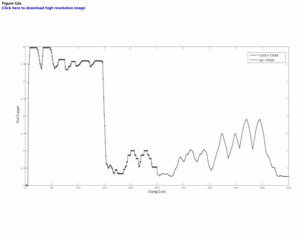
Figure 12aClick here to download high resolution image

Figure 12bClick here to download high resolution image