A VERSATILE 3D CALIBRATION OBJECT FOR VARIOUS MICRO-RANGE MEASUREMENT METHODS€¦ · ·...
6
A VERSATILE 3D CALIBRATION OBJECT FOR VARIOUS MICRO-RANGE MEASUREMENT METHODS M. Ritter a *, M. Hemmleb b , O. Sinram b , J. Albertz b and H. Hohenberg a a HPI, Electron Microscopy and Micro Technology Group, D-20251 Hamburg, Germany - (ritter, hohenberg)@hpi.uni-hamburg.de b TU Berlin, Photogrammetry and Cartography, D-10623 Berlin, Germany - (hemmleb, sinram, albertz)@fpk.tu-berlin.de Commission V, WG 1 KEY WORDS: Accuracy, Calibration, Close Range, Comparison, Correction, Microscopy, Orientation, Photogrammetry ABSTRACT: We present a new micrometer-sized 3D calibration structure containing nanomarkers that serve as well distinguishable reference points for the calibration of various 3D micro-range measurement methods, e.g. scanning electron microscopy (SEM) and environmental SEM (ESEM). The 3D calibration object was fabricated using gas-assisted focused ion beam (FIB) metal deposition. This technique proved to be a valuable tool, as it principally allows the construction of variously shaped microstructures that can be perfectly adapted to the special specifications of the sensor to be calibrated. The spatial data of the 38 non-symmetrically distributed nanomarkers were obtained by high-precision atomic force microscopy (AFM). The accuracy of the nanomarker measurement is shown and the efficiency of the calibration is demonstrated by triangulation and spatial intersection. Additionally, alternative micro-range measurement methods, e.g. confocal laser scanning microscopy (CLSM) and scanning profilometry were tested for possible application of the calibration structure. * Corresponding author. 1. INTRODUCTION The importance and number of micro- and nano- technological applications in material science and in life science is rapidly increasing. The 3D analysis of microstructures generated by micro-fabrication as well as the spatial characterization of surface details requires adequate sensors and micro-range measurement methods. In general, all measurement processes are subdivided into contact and non-contact methods. Whereas most close range measurements work with tactile mechanisms or use light waves as information carriers, a variety of methods have been developed for non-contact micro-range measurements. An overview of relevant 3D micro-range measurement methods will be given in chapter 2. A most suitable sensor is the electron microscope. Modern techniques in scanning electron microscopy like ESEM- technology offer the possibility of imaging even hydrated microstructures while maintaining their original 3D topography. The application of photogrammetric methods for the analysis of electron microscopic data has a long tradition and has become the method of choice for the quantitative 3D-reconstruction of SEM or (ESEM) images: SEM data provide a large depth of focus, a high signal to noise ratio and images can be captured over a wide range of magnification. The efficiency of the photogrammetric method has been proved in numerous applications e.g. the characterization of microstructures, the topographic analysis of frictions and the reconstruction of biological surfaces [König et al., 1987, Scherrer et al., 1999, Hemmleb et al., 2000, Hemmleb, 2001, Ritter et al., 2003]. However, quantitative photogrammetric reconstruction of electron microscopic data requires a set of basic components. We recently presented a micrometer-sized 3D calibration structure that allows the calibration of SEM [Sinram et al., 2002a]. Yet, also optical errors of alternative micro-range measurement methods, e.g. ESEM or confocal laser scanning microscopy (CLSM) and scanning profilometry can be detected. The 3D microstructure was fabricated using gas-assisted focused ion (FIB) beam technique. Based on this technique, an optimally designed 3D micro-object was created. The subsequent high precision spatial measuring with atomic force microscopy (AFM) made a calibration object out of the fabricated structure. Here, we describe a method which makes it possible to build 3D structures of various size with a flexible design in order to fit specific applications. Multiple sensors could be calibrated and thus a comparative analysis of the quantitative microscopic data and their significance can be accomplished. Thus, we will give a short overview of 3D micro-range measurement methods connected to this work. 2. SENSORS AND METHODS FOR 3D MICRO RANGE MEASUREMENTS 2.1 Overview Micro-Range Measurement Methods Non-destructive 3D micro-range measurement methods exist in a great variety. For the determination of material parameters, typically tactile methods are chosen. Optical measurement methods are used for 3D surface or volumetric measurements. Various optical measurement techniques were adapted to micro-range requirements. For higher resolutions, methods are needed, which overcome the borders of light microscopy. Using electrons for imaging, the determination of 3D information results from image processing methods, e.g. photogrammetric or tomographic algorithms. Electron beam imaging in combination with 3D image processing
Transcript of A VERSATILE 3D CALIBRATION OBJECT FOR VARIOUS MICRO-RANGE MEASUREMENT METHODS€¦ · ·...
A VERSATILE 3D CALIBRATION OBJECT FOR VARIOUS MICRO-RANGEMEASUREMENT METHODS
M. Ritter a *, M. Hemmleb b, O. Sinram b, J. Albertz b and H. Hohenberg a
a HPI, Electron Microscopy and Micro Technology Group, D-20251 Hamburg, Germany -(ritter, hohenberg)@hpi.uni-hamburg.de
b TU Berlin, Photogrammetry and Cartography, D-10623 Berlin, Germany -(hemmleb, sinram, albertz)@fpk.tu-berlin.de
Commission V, WG 1
KEY WORDS: Accuracy, Calibration, Close Range, Comparison, Correction, Microscopy, Orientation, Photogrammetry
ABSTRACT:
We present a new micrometer-sized 3D calibration structure containing nanomarkers that serve as well distinguishablereference points for the calibration of various 3D micro-range measurement methods, e.g. scanning electron microscopy (SEM)and environmental SEM (ESEM). The 3D calibration object was fabricated using gas-assisted focused ion beam (FIB) metaldeposition. This technique proved to be a valuable tool, as it principally allows the construction of variously shapedmicrostructures that can be perfectly adapted to the special specifications of the sensor to be calibrated. The spatial data ofthe 38 non-symmetrically distributed nanomarkers were obtained by high-precision atomic force microscopy (AFM). Theaccuracy of the nanomarker measurement is shown and the efficiency of the calibration is demonstrated by triangulation andspatial intersection. Additionally, alternative micro-range measurement methods, e.g. confocal laser scanning microscopy(CLSM) and scanning profilometry were tested for possible application of the calibration structure.
* Corresponding author.
1. INTRODUCTION
The importance and number of micro- and nano-technological applications in material science and in lifescience is rapidly increasing. The 3D analysis ofmicrostructures generated by micro-fabrication as well as thespatial characterization of surface details requires adequatesensors and micro-range measurement methods. In general,all measurement processes are subdivided into contact andnon-contact methods. Whereas most close rangemeasurements work with tactile mechanisms or use lightwaves as information carriers, a variety of methods havebeen developed for non-contact micro-range measurements.An overview of relevant 3D micro-range measurementmethods will be given in chapter 2.
A most suitable sensor is the electron microscope. Moderntechniques in scanning electron microscopy like ESEM-technology offer the possibility of imaging even hydratedmicrostructures while maintaining their original 3Dtopography. The application of photogrammetric methodsfor the analysis of electron microscopic data has a longtradition and has become the method of choice for thequantitative 3D-reconstruction of SEM or (ESEM) images:SEM data provide a large depth of focus, a high signal tonoise ratio and images can be captured over a wide range ofmagnification. The efficiency of the photogrammetricmethod has been proved in numerous applications e.g. thecharacterization of microstructures, the topographic analysisof frictions and the reconstruction of biological surfaces[König et al., 1987, Scherrer et al., 1999, Hemmleb et al.,2000, Hemmleb, 2001, Ritter et al., 2003].
However, quantitative photogrammetric reconstruction ofelectron microscopic data requires a set of basiccomponents. We recently presented a micrometer-sized 3D
calibration structure that allows the calibration of SEM[Sinram et al., 2002a]. Yet, also optical errors of alternativemicro-range measurement methods, e.g. ESEM or confocallaser scanning microscopy (CLSM) and scanningprofilometry can be detected. The 3D microstructure wasfabricated using gas-assisted focused ion (FIB) beamtechnique. Based on this technique, an optimally designed3D micro-object was created. The subsequent high precisionspatial measuring with atomic force microscopy (AFM) madea calibration object out of the fabricated structure.
Here, we describe a method which makes it possible to build3D structures of various size with a flexible design in orderto fit specific applications. Multiple sensors could becalibrated and thus a comparative analysis of thequantitative microscopic data and their significance can beaccomplished. Thus, we will give a short overview of 3Dmicro-range measurement methods connected to this work.
2. SENSORS AND METHODS FOR 3D MICRO RANGEMEASUREMENTS
2.1 Overview Micro-Range Measurement Methods
Non-destructive 3D micro-range measurement methods existin a great variety. For the determination of materialparameters, typically tactile methods are chosen. Opticalmeasurement methods are used for 3D surface or volumetricmeasurements. Various optical measurement techniques wereadapted to micro-range requirements. For higher resolutions,methods are needed, which overcome the borders of lightmicroscopy. Using electrons for imaging, the determinationof 3D information results from image processing methods,e.g. photogrammetric or tomographic algorithms. Electronbeam imaging in combination with 3D image processing
offers the possibility to bridge optical 3D measurementmethods and scanning probe microscopy. For a betterunderstanding, 3D measurement methods in micro-range aredivided into surface und volumetric methods. An overviewof important techniques is given in Table 1. The next twochapters will deal with an overview of relevant micro-rangemeasurement methods.
Surface measurementmethods
Volumetricmeasurement
methodsProfilometry (optical
or mechanical)Light Microscopy and
shape from focusMicro-optical
triangulation methods(structured light)
Confocal LaserScanning Microscopy
(CLSM)(Environmental)
Scanning ElectronMicroscopy ([E] SEM)
combined withphotogrammetry
TransmissionElectron Microscopy
(TEM) andtomographical
methodsAtomic Force
Microscopy (AFM)Micro-Tomography
(Micro CT)(Laser-) Interferometry
Table 1. 3D micro-measurement methods
2.2 Surface measurement
Scanning Electron Microscope and Photogrammetry
The electron microscope uses electrons instead of light forimaging. In scanning electron microscopy, the signal of asample surface is generated by an accelerated electron beamthat is scanned over a sample surface “line by line”. Thereby,electrons of the primary beam interact with the atoms of thesurface. In elastic and inelastic scattering processes,electrons of a broad energy spectrum are emitted from thesample surface. Two different types of emitted electrons arecommonly used for imaging: Secondary (SE) andBackscattered (BSE) electrons. SE are created in the sampleitself and only capable to leave it, if generated in the firstfew nanometres. Therefore, SE carry the high-resolutioninformation. SE emitted from the sample are detected by aphotomultiplier system. The signal is then converted to adigital grey-scale image with an analogue-digital-adapter.What makes the SEM so valuable for micro-rangemeasurements are the topographic details of the scannedimages and the large depth of focus. Also, SEM provides afairly high resolution due to the properties of the electronoptical system. Although the wavelength of the electronscould be in the picometer range, due to lens aberration theaperture of the magnetic lenses of electron microscopes mustnot exceed values of about 10-2 rad (0.7 - 1.3 rad in lightoptics). This limitation results in a maximum resolution inthe nanometer range. The depth of focus is also affected bythe electron-probe aperture and is quite large incorrespondence to the small aperture. The depth of focus of aSEM is at least 10 times the depth of focus of the LM. Athigh magnification it still is in the micrometer range. Thisfact had to be considered when planning size and shape ofthe calibration object.
A specific feature of image acquisition with the SEM is theformation of very long focal length in combination with avirtual projection centre. Therefore, the image process i sdescribed with parallel geometry. Magnification andworking distance, which is the distance between the electron
emission pole and the specimen, have to remain constantduring image acquisition for photogrammetric evaluation.Photogrammetric processing software has to take intoaccount the special properties of SEM imaging describedabove. In order to increase the accuracy of 3D pointdetermination, a bundle adjustment with should be applied[Maune 1976, Ghosh et al., 1976, El Ghazali 1984, Hemmleb2001]. At magnifications higher than 500, usually parallelprojection equations are used. The bundle adjustmentapproach also offers the possibility for photogrammetriccalibration of SEM. With the known calibration parametersof the SEM and defined rules for the image data acquisition,the photogrammetric processing of surface models requiresmostly only two images. They have to be achieved by tiltingthe sample on a suitable working stage [Sinram et al.,2002b].
The calibration of SEM includes at least the determination ofthe particular magnification (image scale) and the tiltingangles. Depending on the chosen imaging model, the focallength has to be calculated too. Because of the necessity torotate the sample in a fixed imaging system (like the SEM)the calibration data describe the motion of the workingstage. The calibration of the SEM should be repeated fromtime to time, because the conditions of image acquisition donot remain constant in electron microscopy.
Environmental Scanning Electron Microscope (ESEM) andPhotogrammetry
A special kind of scanning electron microscopy techniquethat operates at high pressures was introduced 1979 byDanilatos [Danilatos et al., 1979]. On the one hand, thetechnique allowed to look at liquid and hydrated samplesand it simplified the preparation of the specimen. Theapproach was optimized by FEI Company (Eindhoven,Netherlands) and is offered under the name “environmentalscanning electron microscope” (ESEM). The ESEM operatesat pressures of 0.1 to about 20 Torr in its specimen chamber.The minimum pressure to keep water in the liquid phase at4°C is 6.1 Torr. A multiple pressure limiting aperture system(PLA) supplemented by a gaseous secondary electron (GSE)detector enables the ESEM to work under such conditionsThe PLA system allows a high water pressure in the specimenchamber without affecting the high vacuum at the top of themicroscope column, where the electron source is located. Itis not possible to use the regular SE detector in a gaseousenvironment. But, the GSE- detector takes advantage of thepresence of gas in the specimen chamber where the SE scatterat the gas molecules present in the specimen chamber. Oneeffect of the collision is the release of more SE from everycollision, thereby provoking a cascade reaction withsufficient SE yield for the GSE detector. The ESEM isfrequently used in material research, dental research andmore and more in the field of life sciences.
Atomic Force Microscopy
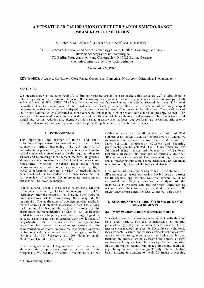
Atomic Force Microscopy (AFM), also known as ScanningForce Microscopy (SFM) belongs to the methods ofScanning Probe Microscopy (SPM). The AFM measuresatomic interactions between the sample surface and theprobe head.
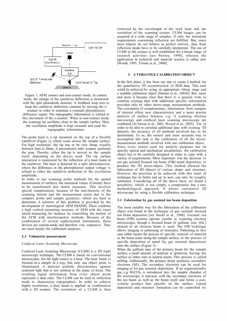
Figure 1. AFM contact and non-contact mode. In contactmode, the change of the cantilever deflection is monitoredwith the split photodiode detector. A feedback loop tries to
keep the cantilever deflection constant by moving the z-scanner in order to maintain a constant photodetector
difference signal. The topographic information is related tothis movement of the z-scanner. When in non-contact mode,the scanning tip oscillates close to the sample surface. Here
the oscillation amplitude is kept constant and used fortopographic information.
The probe head is a tip mounted on the top of a flexiblecantilever (Figure 1), which scans across the sample surface.For high resolution, the tip has to be very sharp, usuallybetween 2nm to 20nm. A piezoelectric tube scanner performsthe scan. Thereby, either the tip is moved or the sampleitself, depending on the device used. The tip surfaceinteraction is monitored by the reflection of a laser beam atthe cantilever. The laser is detected by a split photodetector,where the difference in the photodetector output voltage i srelated to either the cantilever deflection or the oscillationamplitude.In order to use scanning probe methods for the spatialmeasurement of surfaces, the measured values (Current) haveto be transformed into metric measures. This involvesspecial complications, because of the non-linearity of thescanning motion and the measurement errors due to thecomplex probe and sample geometry, which are hard todetermine. A solution of this problem is provided by thedevelopment of metrological AFM (MAFM). These combinea high vertical measuring accuracy of AFM with the exactlateral measuring, for instance by controlling the motion ofthe AFM with interferometric methods. Because of thecombination of several sophisticated instruments, thesedevices are custom-made and therefore very expensive. Theyare used mainly for calibration purposes.
2.3 Volumetric measurement
Confocal Laser Scanning Microscopy
Confocal Laser Scanning Microscopy (CLSM) is a 3D lightmicroscopy technique. The CLSM is based on conventionalmicroscopes, but the light source is a laser. The laser beam isfocused on a sample in a way, that only one object point i silluminated. A detector pinhole discriminates againstscattered light that is not emitted in the plane of focus. Theresulting signal information from every object pointrepresents a data cube. The CLSM can be used in reflectionmode to characterize topographies. In order to achievehigher resolutions, a laser beam is applied in combinationwith a 3D scanner. The resolution of a CLSM is then
restricted by the wavelength of the used laser and theresolution of the scanning system. CLSM images can beacquired of a wide range of samples, if only the minimumrequirements concerning reflection are fulfilled. But, sincemost objects do not behave as perfect mirrors, data fromreflection mode have to be carefully interpreted. The use ofCLSM in life science is well established for a broad range ofresearch activities [see Pawley, 1990], whereas theapplication in technical and material science is rather new[Wendt, 1995, Tiziani et al., 2000].
3. A VERSATILE CALIBRATION OBJECT
In the first place, it has been our aim to create a method forthe quantitative 3D reconstruction of SEM data. This taskcould be achieved by using an appropriate tilting stage anda suitable calibration object [Sinram et al., 2002b]. But, moreand more it became clear that there is a general wish tocombine existing data with additional specific informationprovided only by other micro-range measurement methods.The correlation of complementary information from samplesof interest offers new characteristics and a more preciseanalysis of surface features, e.g. if scanning electronmicroscopy and confocal laser scanning microscopy arecombined [Al Nawas et al., 2001, Wessel et al., 2003]. Yet, inorder to be able to correlate additional data with existing 3Ddatasets, the accuracy of all methods involved has to bedetermined. To us, the easiest and most accurate way toaccomplish this task is the calibration of all the micro-measurement methods involved with one calibration object.Since every sensor used for analytic purposes has itsspecific optical and mechanical peculiarities, the calibrationobject has to be carefully designed in order to cope with avariety of requirements. Most important was the decision touse gas assisted focused ion beam (FIB) metal deposition toproduce the 3D micro-object. This method allowed thefabrication of 3D objects of various shape and structure.However, the precision to be achieved with this kind oftechnique has its limits and up to now, can only be roughlyestimated. Considering all of the above facts, we found apossibility, which is not simply a compromise but a newmethodological approach. It allows correlative 3Dmicroscopy by using a flexible calibration technique.
3.1 Fabrication by gas assisted ion beam deposition
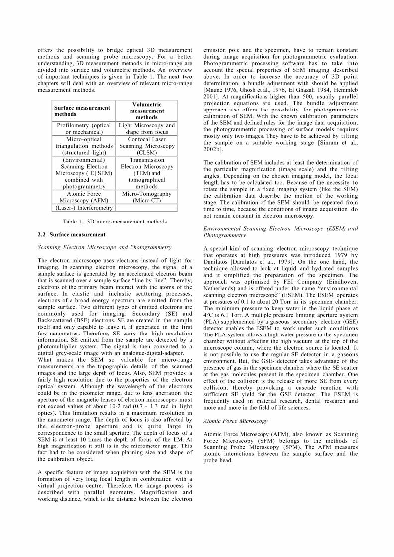
The most suitable way for the fabrication of the calibrationobject was found in the technique of gas assisted focusedion beam deposition [see Steckl et al., 1988]. Focused ionbeam (FIB) systems operate similar to scanning electronmicroscopes, though a focused beam of gallium ions (Ga+)instead of an electron beam is used. The FIB techniqueallows imaging or patterning of structures. Patterning in thiscase either means the process of specific removal of materialas the beam scans along the sample surface, or the process ofspecific deposition of metal (by gas assisted deposition)onto the surface (Figure 3).When the gallium ions of the primary beam hit the samplesurface, a small amount of material is sputtered, leaving thesurface as either ions or neutral atoms. This process is calledmilling. Additionally, the primary beam produces secondaryelectrons (SE). The secondary electrons can be used forimaging or for gas assisted deposition. If an organometallicgas, e.g. W(CO)6 is introduced into the sample chamber ofthe microscope, it interacts with the secondary electrons ofthe ion beam as well as the beam itself and forms a non-volatile product that adsorbs on the surface. Lateraldeposition and structure formation can be controlled by
blanking and unblanking the beam at specific lateralcoordinates (Figure 2). Repetitive scanning of the ion beamin presence of the gas then results in the construction of amultilayer metal film of determined height and form, in ourcase the slope step pyramidal structures.
Figure 2. Schematic drawing of the two patterning modes offocused ion beam (FIB) systems. In the left drawing, the
process of milling is shown. In the right drawing, theprocess of deposition is shown. The deposition product is a
layer of metal, usually tungsten (W) or platinum (Pt). Themetal is introduced into the specimen chamber as an
organometallic compound. It is applied very close to thesample surface through a valve needle with a very fine tip. Ifhit by the ion beam or the secondary electrons generated by
the beam at the sample surface, the organometallic gasdecomposes, whereby the metal deposits at the sample
surface.
3.2 Design and specification
The development and design of the calibration object wasdetermined by the various demands of the particularmeasurement methods (Figure 3).
Figure 3. SEM image of a calibration pyramid made with thetechnique of gas assisted FIB. The pyramidal shaped
calibration object with slope steps approximately measures6µm in width and length and 3µm in height. It can be usedfor SEM calibration at magnifications of 8000x to approx.
20000x. The calibration object has up to 38 nanomarkers ascontrol points. They were applied using FIB milling. The
distribution of the nanomarkers is non-symmetrical, so theycan always be clearly identified and associated.
Also, the peculiarities of the calibration process itself had tobe taken into consideration. In general, it is an advantage in3D measurement methods, if the calibration object coversthe measurement volume. This is especially important in 3Dmeasurements with SEM, because the positioning of thecalibration object is restricted by the properties of thesample and the tilting stage.
Nanomarkers [Hemmleb et al., 1995, Sinram et al., 2002b] onthe calibration object serve as control points carrying thespatial information. They must be easy to detect as discretepoints in both, the scanning electron microscope and theatomic force microscope. The distribution on the lower levelis non-symmetrical, in order to be always informed of thepyramid’s orientation. The control points are detected viasemi-automated image processing methods. Therefore, theircoordinates can be directly used for the photogrammetricbundle block adjustment. The cascade pyramidal shape ofthe calibration structure allows the usage at a range ofmagnifications. Together with the sloping edges, it i sguaranteed that the control points on a lower level maintainvisible, even if tilted in the SEM for the calibration process.Additionally, the angle of the pyramidal cascade step slopes,in respect to the surface plane was designed to be smallerthan the aperture angle of the AFM tip.We wanted to be able to calibrate the SEM at a maximumrange of magnification. Therefore, the measures had torepresent a structure that is still completely within the rangeof the depth of focus, when filling the field of view of anSEM image. Most AFM scanners can handle a scan area up to100µm with a maximum structure elevation of about 8µm.Therefore the size of the calibration structure was limited bythe specifications of the AFM scanner and the opticallimitations of the SEM.
3.3 Application for correlative measurements
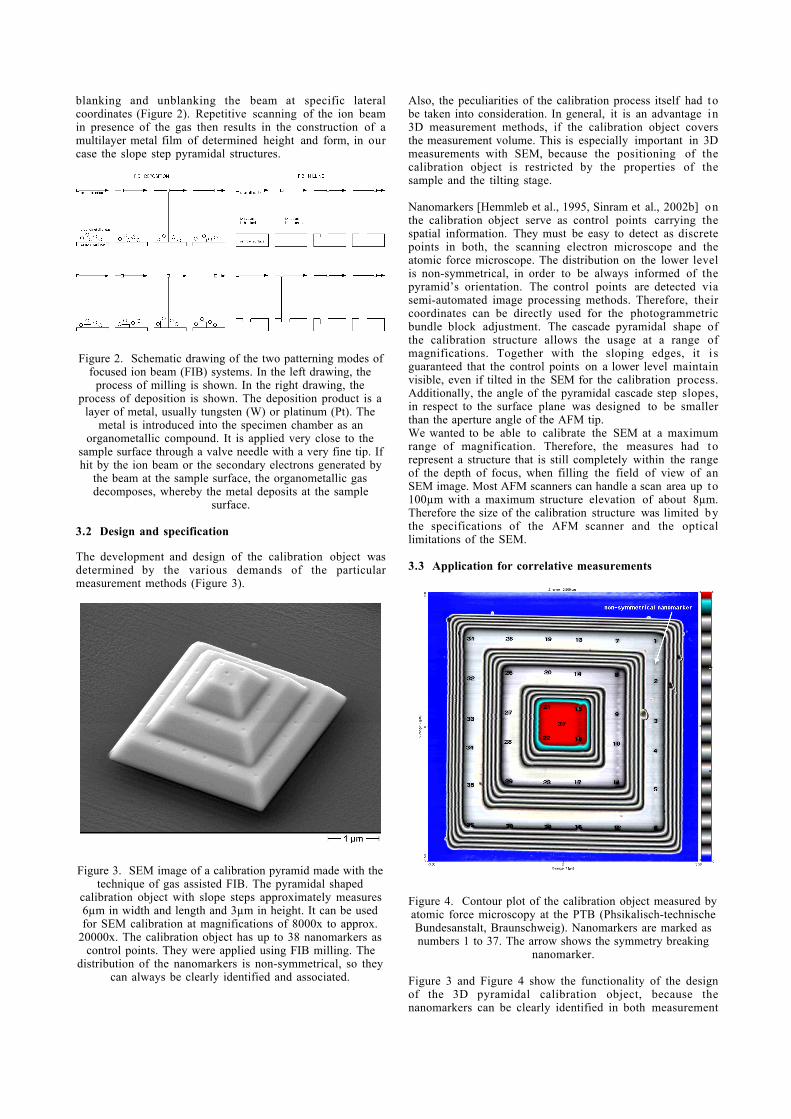
Figure 4. Contour plot of the calibration object measured byatomic force microscopy at the PTB (Phsikalisch-technischeBundesanstalt, Braunschweig). Nanomarkers are marked asnumbers 1 to 37. The arrow shows the symmetry breaking
nanomarker.
Figure 3 and Figure 4 show the functionality of the designof the 3D pyramidal calibration object, because thenanomarkers can be clearly identified in both measurement
methods. Additionally, the pyramidal structure can be tiltedin the SEM for calibration purposes with still all ofnanomarkers visible to the electron beam. Also, due to theslope steps of the calibration object, AFM measurements arepossible and provide the spatial information of the referencepoints that is needed for the calibration of scanning electronmicroscopes.
4. MEASUREMENT RESULTS
4.1 AFM measurement results
High precision AFM measurements in non-contact modewere done at the PTB (Physikalisch-TechnischeBundesanstalt, Braunschweig, Germany). The instrumentused was a modificated SIS-AFM Nanostation III (SIS,Herzogenrath, Germany) with strain gauges in z-directionand lateral capacitive sensors to guarantee lateral high-precision measurements. Although the device is notapproved for metrological measurements, results within 1%of uncertainty in z-direction can be expected.Alternatively, the nanomarker coordinates were measuredwith a “normal”, commercially available Veeco Explorer2000 (Veeco, Woodburry, USA) AFM in contact mode.Nanomarker coordinates of all measurements were detectedusing a geometric search routine, sensitive to suddenchanges in altitude on smooth topographies. Then, the highprecision SIS-AFM data were compared with the raw andcorrected data of the Explorer AFM (Table 2 and Figure 5).Determination of the coordinates of the nanomarkersdepends on the accuracy of the sensor as well as on theaccuracy of the analysis used. From the analysis, a lateralmean point error of 0.9 Pixel has been evaluated,corresponding to a relative error of 0.0009 in a 1000 pixelscan. The relative vertical error is about 0.002. Therefore, thesensor is the limiting factor. This can be clearly seen, whencomparing the accuracy of the high-precision SIS-AFM witha commercially available AFM, e.g. the Veeco Explorer weused in our first approaches for reference pointdetermination. Further improvements will be possible bymeasuring with an interferometrically controlled,metrological AFM (MAFM).
AFMSensor
SA = relative SensorAccuracy
rel. SA + Nanomarkerdetermination error
∆x ∆y ∆z mx my mz
SIS 5*10-4 0.006 0.01 7*10-4 0.006 0.01Veeco 0.1 0.3 0.06 0.1 0.3 0.06Veecocalibrated
0.013 0.026 0.05 0.013 0.026 0.05
Table 2. The accuracy of the AFM measurements andnanomarker detection.
5. CALIBRATION RESULTS
With the nanomarker coordinates determined by high-precision AFM, we were able to calibrate a high-resolutionfield-emission SEM, the XL30 FEG as well as a XL30 ESEMunder “wet mode” (1 Torr water vapour pressure) conditions.Calibration of the XL30 FEG was performed with 10 imagestilted by steps of 5 degrees. Calibration of the XL30 ESEMwas done with 5 images and arbitrary tilt steps. Tables 3 and4 show the calibrated magnification factor (m), the meanlateral (mX0, mY0) and the mean tilt angle error calculated(mj, mk, mw).
5.1 SEM calibration results
Sensor XL30 FEGscale (m) 0.094 [pixel/nm]mean (mX0, mY0) [nm] 13.03, 13.15 [nm]mean (mj, mk, mw) 0.781, 0.804, 0.248 [deg]
Table 3. Calibration results of the XL30 FEG scanningelectron microscope.
5.2 ESEM calibration results
Sensor XL30 ESEMscale (m) 0.1133 [pixel/nm]mean (mX0, mY0) 10.228, 10.075[nm]mean (mj, mk, mw) 0.643, 0.654, 0.18 [deg]
Table 4. Calibration results of the XL30 ESEM scanningelectron microscope.
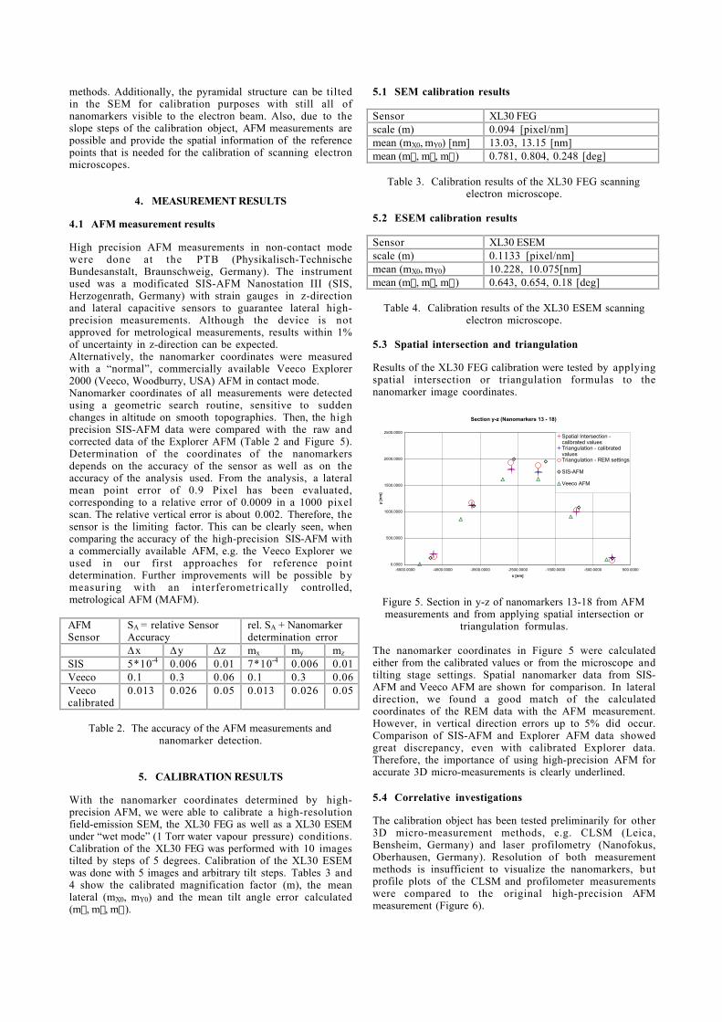
5.3 Spatial intersection and triangulation
Results of the XL30 FEG calibration were tested by applyingspatial intersection or triangulation formulas to thenanomarker image coordinates.
Section y-z (Nanomarkers 13 - 18)
0.0000
500.0000
1000.0000
1500.0000
2000.0000
2500.0000
-5500.0000 -4500.0000 -3500.0000 -2500.0000 -1500.0000 -500.0000 500.0000
x [nm]
y [n
m]
Spatial Intersection -calibrated valuesTriangulation - calibratedvaluesTriangulation - REM settings
SIS-AFM
Veeco AFM
Figure 5. Section in y-z of nanomarkers 13-18 from AFMmeasurements and from applying spatial intersection or
triangulation formulas.
The nanomarker coordinates in Figure 5 were calculatedeither from the calibrated values or from the microscope andtilting stage settings. Spatial nanomarker data from SIS-AFM and Veeco AFM are shown for comparison. In lateraldirection, we found a good match of the calculatedcoordinates of the REM data with the AFM measurement.However, in vertical direction errors up to 5% did occur.Comparison of SIS-AFM and Explorer AFM data showedgreat discrepancy, even with calibrated Explorer data.Therefore, the importance of using high-precision AFM foraccurate 3D micro-measurements is clearly underlined.
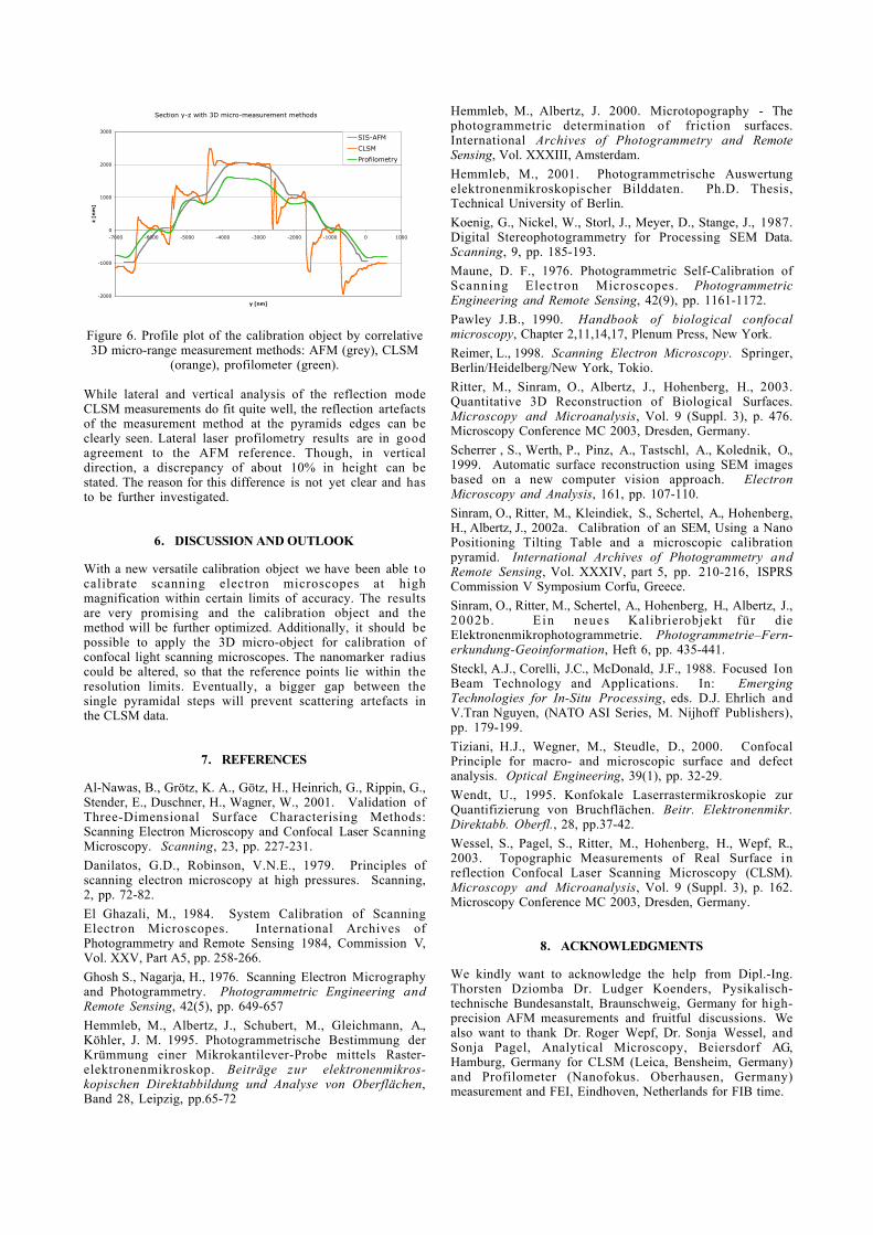
5.4 Correlative investigations
The calibration object has been tested preliminarily for other3D micro-measurement methods, e.g. CLSM (Leica,Bensheim, Germany) and laser profilometry (Nanofokus,Oberhausen, Germany). Resolution of both measurementmethods is insufficient to visualize the nanomarkers, butprofile plots of the CLSM and profilometer measurementswere compared to the original high-precision AFMmeasurement (Figure 6).
Section y-z with 3D micro-measurement methods
-2000
-1000
0
1000
2000
3000
-7000 -6000 -5000 -4000 -3000 -2000 -1000 0 1000
y [nm]
z [n
m]
SIS-AFM
CLSM
Profilometry
Figure 6. Profile plot of the calibration object by correlative3D micro-range measurement methods: AFM (grey), CLSM
(orange), profilometer (green).
While lateral and vertical analysis of the reflection modeCLSM measurements do fit quite well, the reflection artefactsof the measurement method at the pyramids edges can beclearly seen. Lateral laser profilometry results are in goodagreement to the AFM reference. Though, in verticaldirection, a discrepancy of about 10% in height can bestated. The reason for this difference is not yet clear and hasto be further investigated.
6. DISCUSSION AND OUTLOOK
With a new versatile calibration object we have been able tocalibrate scanning electron microscopes at highmagnification within certain limits of accuracy. The resultsare very promising and the calibration object and themethod will be further optimized. Additionally, it should bepossible to apply the 3D micro-object for calibration ofconfocal light scanning microscopes. The nanomarker radiuscould be altered, so that the reference points lie within theresolution limits. Eventually, a bigger gap between thesingle pyramidal steps will prevent scattering artefacts inthe CLSM data.
7. REFERENCES
Al-Nawas, B., Grötz, K. A., Götz, H., Heinrich, G., Rippin, G.,Stender, E., Duschner, H., Wagner, W., 2001. Validation ofThree-Dimensional Surface Characterising Methods:Scanning Electron Microscopy and Confocal Laser ScanningMicroscopy. Scanning, 23, pp. 227-231.
Danilatos, G.D., Robinson, V.N.E., 1979. Principles ofscanning electron microscopy at high pressures. Scanning,2, pp. 72-82.
El Ghazali, M., 1984. System Calibration of ScanningElectron Microscopes. International Archives ofPhotogrammetry and Remote Sensing 1984, Commission V,Vol. XXV, Part A5, pp. 258-266.
Ghosh S., Nagarja, H., 1976. Scanning Electron Micrographyand Photogrammetry. Photogrammetric Engineering andRemote Sensing, 42(5), pp. 649-657
Hemmleb, M., Albertz, J., Schubert, M., Gleichmann, A.,Köhler, J. M. 1995. Photogrammetrische Bestimmung derKrümmung einer Mikrokantilever-Probe mittels Raster-elektronenmikroskop. Beiträge zur elektronenmikros-kopischen Direktabbildung und Analyse von Oberflächen,Band 28, Leipzig, pp.65-72
Hemmleb, M., Albertz, J. 2000. Microtopography - Thephotogrammetric determination of friction surfaces.International Archives of Photogrammetry and RemoteSensing, Vol. XXXIII, Amsterdam.
Hemmleb, M., 2001. Photogrammetrische Auswertungelektronenmikroskopischer Bilddaten. Ph.D. Thesis,Technical University of Berlin.
Koenig, G., Nickel, W., Storl, J., Meyer, D., Stange, J., 1987.Digital Stereophotogrammetry for Processing SEM Data.Scanning, 9, pp. 185-193.
Maune, D. F., 1976. Photogrammetric Self-Calibration ofScanning Electron Microscopes. PhotogrammetricEngineering and Remote Sensing, 42(9), pp. 1161-1172.
Pawley J.B., 1990. Handbook of biological confocalmicroscopy, Chapter 2,11,14,17, Plenum Press, New York.
Reimer, L., 1998. Scanning Electron Microscopy. Springer,Berlin/Heidelberg/New York, Tokio.
Ritter, M., Sinram, O., Albertz, J., Hohenberg, H., 2003.Quantitative 3D Reconstruction of Biological Surfaces.Microscopy and Microanalysis, Vol. 9 (Suppl. 3), p. 476.Microscopy Conference MC 2003, Dresden, Germany.
Scherrer , S., Werth, P., Pinz, A., Tastschl, A., Kolednik, O.,1999. Automatic surface reconstruction using SEM imagesbased on a new computer vision approach. ElectronMicroscopy and Analysis, 161, pp. 107-110.
Sinram, O., Ritter, M., Kleindiek, S., Schertel, A., Hohenberg,H., Albertz, J., 2002a. Calibration of an SEM, Using a NanoPositioning Tilting Table and a microscopic calibrationpyramid. International Archives of Photogrammetry andRemote Sensing, Vol. XXXIV, part 5, pp. 210-216, ISPRSCommission V Symposium Corfu, Greece.
Sinram, O., Ritter, M., Schertel, A., Hohenberg, H., Albertz, J.,2002b. Ein neues Kalibrierobjekt für dieElektronenmikrophotogrammetrie. Photogrammetrie–Fern-erkundung-Geoinformation, Heft 6, pp. 435-441.
Steckl, A.J., Corelli, J.C., McDonald, J.F., 1988. Focused IonBeam Technology and Applications. In: EmergingTechnologies for In-Situ Processing, eds. D.J. Ehrlich andV.Tran Nguyen, (NATO ASI Series, M. Nijhoff Publishers),pp. 179-199.
Tiziani, H.J., Wegner, M., Steudle, D., 2000. ConfocalPrinciple for macro- and microscopic surface and defectanalysis. Optical Engineering, 39(1), pp. 32-29.
Wendt, U., 1995. Konfokale Laserrastermikroskopie zurQuantifizierung von Bruchflächen. Beitr. Elektronenmikr.Direktabb. Oberfl., 28, pp.37-42.
Wessel, S., Pagel, S., Ritter, M., Hohenberg, H., Wepf, R.,2003. Topographic Measurements of Real Surface inreflection Confocal Laser Scanning Microscopy (CLSM).Microscopy and Microanalysis, Vol. 9 (Suppl. 3), p. 162.Microscopy Conference MC 2003, Dresden, Germany.
8. ACKNOWLEDGMENTS
We kindly want to acknowledge the help from Dipl.-Ing.Thorsten Dziomba Dr. Ludger Koenders, Pysikalisch-technische Bundesanstalt, Braunschweig, Germany for high-precision AFM measurements and fruitful discussions. Wealso want to thank Dr. Roger Wepf, Dr. Sonja Wessel, andSonja Pagel, Analytical Microscopy, Beiersdorf AG,Hamburg, Germany for CLSM (Leica, Bensheim, Germany)and Profilometer (Nanofokus. Oberhausen, Germany)measurement and FEI, Eindhoven, Netherlands for FIB time.