A STUDY OF THE SCALING AND ADVANCED FUNCTIONALITY ...
214
1 A STUDY OF THE SCALING AND ADVANCED FUNCTIONALITY POTENTIAL OF PHASE CHANGE MEMORY DEVICES Submitted by Hasan Hayat to the University of Exeter as a thesis for the degree of Doctor of Philosophy (PhD) in Engineering, November 2016. This thesis is available for Library use on the understanding that it is copyright material and that no quotation from the thesis may be published without proper acknowledgement. I certify that all material in this thesis which is not my work has been identified and that no material is included for which a degree has previously been conferred upon me. ...................................... Hasan Hayat
Transcript of A STUDY OF THE SCALING AND ADVANCED FUNCTIONALITY ...

1
A STUDY OF THE SCALING AND ADVANCED FUNCTIONALITY
POTENTIAL OF PHASE CHANGE MEMORY DEVICES
Submitted by
Hasan Hayat
to the University of Exeter as a thesis for the degree of Doctor of Philosophy
(PhD) in Engineering, November 2016.
This thesis is available for Library use on the understanding that it is copyright
material and that no quotation from the thesis may be published without proper
acknowledgement.
I certify that all material in this thesis which is not my work has been identified and
that no material is included for which a degree has previously been conferred upon
me.
......................................
Hasan Hayat

2
Abstract
As traditional volatile and non-volatile data storage and memory technologies such
as SRAM, DRAM, Flash and HDD face fundamental scaling challenges, scientists
and engineers are forced to search for and develop alternative technologies for
future electronic and computing systems that are relatively free from scaling issues,
have lower power consumptions, higher storage densities, faster speeds, and can be
easily integrated on-chip with microprocessor cores. This thesis focuses on the
scaling and advanced functionality potential of one such memory technology i.e.
Phase Change Memory (PCM), which is a leading contender to complement or even
replace the above mentioned traditional technologies.
In the first part of the thesis, a physically-realistic Multiphysics Cellular Automata
PCM device modelling approach was used to the study the scaling potential of
conventional and commercially-viable PCM devices. It was demonstrated that
mushroom-type and patterned probe PCM devices can indeed be scaled down to
ultrasmall (single-nanometer) dimensions, and in doing so, ultralow programming
currents (sub-20 μA) and ultrahigh storage densities (~10 Tb/in2) can be achieved
via such a scaling process. Our sophisticated modelling approach also provided a
detailed insight into some key PCM device characteristics, such as amorphization
(Reset) and crystallization (Set) kinetics, thermal confinement, and the important
resistance window i.e. difference in resistances between the Reset and Set states.
In the second part of the thesis, the aforementioned modelling approach was used to
assess the feasibility of some advanced functionalities of PCM devices, such as
neuromorphic computing and phase change metadevices. It was demonstrated that
by utilizing the accumulation mode of operation inherent to phase change materials,
we can combine a physical PCM device with an external comparator-type circuit to
deliver a ‘self-resetting spiking phase change neuron’, which when combined with
phase change synapses can potentially open a new route for the realization of all-
phase change neuromorphic computers. It was further shown that it is indeed
feasible to design and ‘electrically’ switch practicable phase change metadevices (for
absorber and modulator applications, and suited to operation in the technologically
important near-infrared range of the spectrum).
Finally, it was demonstrated that the Gillespie Cellular Automata (GCA) phase
change model is capable of exhibiting ‘non-Arrhenius kinetics of crystallization’,
which were found to be in good agreement with reported experimental studies.

3
List of Publications
Book Chapters
(1) H. Hayat, K. Kohary and C. D. Wright, “Scaling of Phase Change Materials
and Memory Devices”, (Invited Book Chapter). To be published in Phase
Change Memory: Device Physics, Reliability and Applications. Chapter 9.
(2016). Editor: Andrea Redaelli. Springer Publishing Group. Accepted
Review Papers
(2) H. Hayat, K. Kohary and C. D. Wright, “Emerging Nanoscale Phase-Change
Memories: A Summary of Device Scaling Studies”, Electronic Materials,
Elsevier Reference Module in Materials Science and Materials Engineering,
04144, (2016).
Research Papers
(3) H. Hayat, K. Kohary and C. D. Wright, “Can conventional phase-change
memory devices be scaled down to single-nanometre dimensions?”,
Nanotechnology, 28, 3, (2016).
(4) H. Hayat, K. Kohary and C. D. Wright, “Ultrahigh Storage Densities via the
Scaling of Patterned Probe Phase-Change Memories”, IEEE Transactions on
Nanotechnology, (2017). Accepted
(5) S. G-C. Carrillo, G. R. Nash, H. Hayat, M. J. Cryan, M. Klemm, H. Bhaskaran
and C. D. Wright, “Design of practicable phase-change metadevices for near-
infrared absorber and modulator applications”, Optics Express, 24, 12, (2016).
(6) R. Cobley, H. Hayat, and C. D. Wright, “A self-resetting spiking phase-change
neuron”, European Phase Change and Ovonics Symposium (EPCOS),
Cambridge, (2016).
(7) H. Hayat, K. Kohary and C. D. Wright, “Size Scaling in Phase-Change
Memory Cells: From Traditional to Emerging Device Structures”, European
Phase Change and Ovonics Symposium (EPCOS), Cambridge, (2016).
(8) H. Hayat, K. Kohary and C. D. Wright, “Simulation of Ultrahigh Storage
Densities in Nanoscale Patterned Probe Phase-Change Memories”, IEEE
Nanotechnology Materials and Devices Conference, Toulouse, pp. 1-2,
October, (2016).

4
(9) H. Hayat, K. Kohary and C. D. Wright, “A theoretical study of the scaling
behaviour of mushroom PCRAM devices using the Gillespie Cellular
Automata Approach”, European Phase Change and Ovonics Symposium
(EPCOS), Amsterdam, (2015).
(10) R. Cobley, H. Hayat, and C. D. Wright, “Self-resetting Spiking Neurons for
Neuromorphic Computing Applications using Nanoscale Phase-Change
Memory Devices”, Submitted to Nanotechnology
(11) H. Hayat, K. Kohary and C. D. Wright, “Modelling the Non-Arrhenius Kinetics
of Crystallization in Phase-Change Materials using the Gillespie Cellular
Automata Approach”, Manuscript in preparation
Attended Conferences and Events
(1) IEEE Nanotechnology Materials and Devices, Toulouse, France. October 2016
(Oral presentation).
(2) European Phase Change and Ovonics Symposium (EPCOS), Cambridge, UK.
September 2016 (Poster presentation).
(3) European Phase Change and Ovonics Symposium (EPCOS), Amsterdam,
Netherlands. September 2015 (Poster presentation).
(4) Chalcogenide Advanced Manufacturing Partnership (ChAMP), University of
Southampton, UK. March 2015.
(5) Defence Materials Forum (DMF), University of Exeter, UK. May 2016 (Poster
presentation).
(6) Early Career Researcher Networking (ECRN) Sessions, University of Exeter,
UK. 2016 (Poster presentation).

5
Table of Contents
Abstract…………………………………………………………………………………. 2
List of Publications………..………………………………………………………….. 3
Table of Contents……………………………………………………………………… 5
List of Figures……………...………………………………………………………….. 8
List of Tables…………….....………………………………………………………….. 17
Acknowledgements…………………………………………………………………… 18
Chapter 1 Introduction and Motivation……………….................................... 19
1.1 Overview of Data Storage and Memory Technologies..................... 20
1.1.1 Traditional Memory Technologies.......................................... 21
1.1.2 Emerging Memory Technologies........................................... 26
1.2 Phase Change Memory (PCM)........................................................ 31
1.2.1 Background and Commercialization of PCM......................... 31
1.2.2 Phase Change Memory: Operation Principle........................ 33
1.2.3 Threshold Switching.............................................................. 34
1.2.4 PCM Device Structures and Scaling Characteristics............. 35
1.3 Phase Change Materials: Characteristics and Properties................ 36
1.3.1 Key Features of Phase Change Materials............................. 37
1.3.2 Key Properties of Phase Change Materials........................... 38
1.3.3 Scaling of Phase Change Materials....................................... 38
1.4 Advanced Functionalities of Phase Change Materials and
Memory Devices............................................................................... 39
1.4.1 Neuromorphic (Brain-inspired Computing)............................ 39
1.4.2 In-Memory Processing: Beyond Von-Neumann Computing.. 40
1.4.3 Phase Change Metamaterials and Metadevices.................... 41
1.5 Project Aim and Contribution to Knowledge...................................... 44
1.6 Thesis synopsis................................................................................. 46
Chapter 2 A Review of Scaling in Phase Change Memory Materials
and Devices………………................................................................ 49
2.1 Scaling of Phase Change Materials................................................... 51
2.1.1 Material Scaling in One Dimension......................................... 52
2.1.2 Material Scaling in Two Dimensions....................................... 55

6
2.1.3 Material Scaling in Three Dimensions..................................... 58
2.2 Scaling of Phase Change Memory Devices....................................... 61
2.2.1 The ‘Mushroom’ Cell................................................................ 61
2.2.2 The μTrench and Dash-type Cell............................................. 69
2.2.3 The Pore Cell........................................................................... 70
2.2.4 Crossbar Cells......................................................................... 73
2.2.5 Probe-based Phase Change Memory Cells............................ 74
2.2.6 Carbon Nanotube-based Cells................................................ 79
2.3 The Role of Thermal Engineering in Scaling...................................... 80
2.4 Chapter Summary............................................................................... 82
Chapter 3 Simulation of Phase Change Devices using a Multiphysics
Cellular Automata Approach…………………………………………. 84
3.1 Electrical Model.................................................................................. 85
3.2 Thermal Model................................................................................... 87
3.3 A Review of Phase Change Models................................................... 88
3.3.1 Classical Nucleation-Growth Theory....................................... 88
3.3.2 Johnson-Mehl-Avrami-Kolmogorov (JMAK) Model................. 90
3.3.3 Rate Equation-based Methods................................................ 91
3.3.4 Atomistic Modelling.................................................................. 93
3.3.5 Gillespie Cellular Automata (GCA) Model............................... 94
3.3.6 Summary and Comparison of Phase Change Models........... 101
3.4 Implementation of the Multiphysics Cellular Automata Approach for
PCM Device Simulations................................................................... 102
3.5 Chapter Summary............................................................................. 107
Chapter 4 The Scaling Characteristics of Conventional Mushroom-type
Phase Change Memory Devices.................................................... 108
4.1 Introduction....................................................................................... 108
4.2 Methodology...................................................................................... 110
4.3 Results.............................................................................................. 113
4.3.1 The Reset process in nanoscaled PCM cells........................ 113
4.3.2 The Set process in nanoscaled PCM cells............................. 121
4.4 Resistance Window and Reset Current............................................ 127
4.5 Chapter Summary and Conclusions................................................. 132

7
Chapter 5 Ultrahigh Storage Densities via the Scaling of Patterned
Probe Phase Change Memories.................................................. 134
5.1 Introduction..................................................................................... 134
5.2 Methodology................................................................................... 135
5.3 Results and Discussion.................................................................. 138
5.3.1 Comparison of PP-PCM Cell Structures.............................. 138
5.3.2 Scaling Characteristics of PP-PCM Cells............................ 146
5.3.3 Storage Densities in PP-PCM Cells..................................... 151
5.4 Chapter Summary and Conclusions............................................... 155
Chapter 6 Self-Resetting Spiking Phase Change Neurons for
Neuromorphic Computing Applications..................................... 157
6.1 Introduction..................................................................................... 158
6.2 Methodology................................................................................... 159
6.3 Results and Discussion.................................................................. 161
6.4 Chapter Summary and Conclusions............................................... 172
Chapter 7 Electrical Switching in Phase Change Metadevices for
Near-infrared Absorber and Modulator Applications................ 174
7.1 Introduction..................................................................................... 175
7.2 Methodology................................................................................... 176
7.3 Results and Discussion.................................................................. 178
7.3.1 Choice of Material Layers for Modulator structure............... 178
7.3.2 Electrical Switching.............................................................. 180
7.4 Chapter Summary and Conclusions............................................... 184
Chapter 8 Non-Arrhenius Kinetics of Crystallization in Phase Change
Materials........................................................................................ 185
8.1 Introduction..................................................................................... 185
8.2 Methodology................................................................................... 188
8.3 Results and Discussion................................................................... 189
8.4 Chapter Summary and Conclusions............................................... 193
Chapter 9 Conclusions and Future Outlook................................................. 194
Bibliography...………………………..………………………………………….…….. 201

8
List of Figures
1.1 The growth rate of global digital data per year……………………………….. 19
1.2 Memory taxonomy showing various memory technologies………............... 20
1.3 (a) Physical distribution and hierarchy of memory in a computer.
(b) Schematic of a circuit of a SRAM cell consisting of six transistors.
(c-d) Schematics of DRAM and Flash memories.
(e) Schematic of a typical hard disk.............................................................. 23
1.4 FeRAM schematic cross-section and basic working principle...................... 27
1.5 (a) Basic functioning of MRAM. (b) Conventional MRAM
device structure vs STT-RAM device structure............................................ 28
1.6 (a) Schematic of a RRAM cell. (b) RRAM switching mechanism................. 29
1.7 (a) Schematic of a typical PCM ‘mushroom’ cell.
(b) Reversible switching in PCM between an ‘orderly’ crystalline
phase, and ‘disorderly’ amorphous phase using Set and Reset
pulses respectively....................................................................................... 33
1.8 Typical current-voltage (I-V) curve for a PCM cell
showing the threshold voltage (Vth).............................................................. 34
1.9 Taxonomy of various ‘Traditional’ and ‘Emerging’ PCM
cell structures................................................................................................ 36
1.10 (a) The ternary Ge-Sb-Te phase diagram with some popular
phase change alloys highlighted. (b) A map of Te-based phase
change materials as a function of material ionicity & hybridization............... 37
1.11 Bioinspired electronic synapses.................................................................... 40
1.12 Schematic of the PCM mushroom cell used by Wright et al for
simulations of the phase-change base-10 accumulator response…….…… 42
1.13 (a) All-optical non-volatile, chalcogenide metamaterial switch
reported by Gholipour et al. (b) Schematic of the phase
change metamaterial absorber structure presented by Cao et al................. 43
2.1 (a) Historic trend in the semiconductor device technology
node F (numbers on the plot refer to F value in nanometres).
(b) Schematic of a generic device layout showing device pitch of
F, and so smallest device area at node F equal to 4F2……………….……… 50

9
2.2 (a) Variation of crystallization temperature as a function of film
thickness for various phase change materials.
(b) Variation of crystallization and melting temperatures
(Tx and Tm) versus film thickness for GeTe films……………………………. 52
2.3 (a) SEM image of as-grown Ge2Sb2Te5 nanowires. (b) The
variation in amorphization current and power as a function
of Ge2Sb2Te5 nanowire diameter……………………………………………… 56
2.4 (a) Amorphization current densities in GeTe nanowires. (b) GeTe
nanowires grown inside a 1.3 nm CNT template……………………………. 57
2.5 (a) TEM image of an annealed (crystallized) GeSb nanoparticle.
(b) Variation of crystallization temperature as a function of
nanoparticle diameter for ultra-small GeTe nanoparticles. (c) TEM
images of as-deposited amorphous and spherical nanoclusters……….….. 58
2.6 (a) Predicted (via classical nucleation-growth theory the minimum
stable crystallite cluster size for Ge2Sb2Te5 as a function of temperature
(b) Atomic configurations during the crystallization process in
amorphous Ge2Sb2Te5 and the evolution of structural units on
annealing at 600 K …………………………………………………………….... 60
2.7 TEM Cross-section of a mushroom type PCM cell showing the
rounded amorphous dome formed above the heater………………………... 62
2.8 Schematic of a PCM cell showing key geometrical and physical
parameters used in the analytical study of Russo et al………………….…... 63
2.9 (a) Variation of PCM mushroom-type cell ON resistance as a function
of the technology node size (F). (b) Variation in the melting (Reset)
current as a function of the technology node (F)…………………………..…. 66
2.10 (a) The variation of melting current, Im, as a function of heater length, Lh.
(b) Simulated temperature distributions in mushroom-type PCM cells
(each subject to their own individual melting current) with different
Lc and Lh sizes………………………………………………………………..…... 67
2.11 (a) A 90 nm node mushroom-type PCM as developed by IBM to deliver
multi-level storage capability of up to 3-bits per cell. (b) Programming
current versus resistance curve for multi-level operation showing use of
partial Reset to provide multiple resistance levels…………………….……… 69

10
2.12 (a) Simulated Reset current amplitude as a function of the size of
the bottom electrical contact (BEC) for a mushroom-type cell
(planar structure) and a confined cell, showing expected reduction
in Reset current for the latter. (b) Schematic of the dash-type version
of the confined cell as developed by Samsung. (c) TEM cross-
sectional image of a dash-type cell………………………………………….. 70
2.13 (a) TEM cross-sectional image of a GST pore-type cell. (b) Simulation
of temperature distribution in GST layer during RESET process,
showing successful confinement of the heated volume. (c) Simulated
effect of pore diameter and slope of SiN sidewall on Reset current……… 71
2.14 (a) Set voltage versus pulse width for pore-type cells of 50 nm in
diameter with and without the aid of a 0.3 V “incubation-field”.
(b) Shows successful repeated switching of the cell in (a) with 500 ps
pulses for both Set and Reset…………………………………………………. 72
2.15 (a) Schematic of a crossbar type PCM structure with integrated Si-diode
selector. (b) TEM cross-sectional image of a crossbar device.
(c) Reset current scaling characteristics of a PCM crossbar device
showing a ten-fold reduction in current as the contact size shrinks
from 150 nm to 30 nm…………………………………………………………… 73
2.16 (a) The IBM ‘Millipede’ concept consisting of a 2-D array of probes
used to write, read and erase indentations in polymer media
(b) Experimental setup by Hamann et al for phase change thermal
recording (top), and crystalline bits written in an amorphous GST film
using a heated AFM tip (bottom), achieving storage densities of up
to 3.3. Tb/in2……………………………………………………………………… 75
2.17 (a) Schematic of the write (top) and read (bottom) processes in phase
change probe storage. (b) Phase change probe memory cell structure
used by Wright et al. to demonstrate 1.5 Tb/in2 storage densities………….. 75
2.18 (a) Schematic diagram of patterned probe PCM (PP-PCM) cells
proposed by Kim et al. to demonstrate electrical switching on the
micrometer scale. (b) SEM image of the 2D-arrayed PP-PCM cells……….. 77

11
2.19 (a) AFM images of a CNT-based nanogap PCM cell before and after
filling with GST (the scale bars are 500 nm). (b) Ultra-low programming
currents achieved for several CNT-based nanogap PCM devices
having ultra-small contact diameters……………………………………….…. 79
2.20 (a) Stacked TiN/W electrode structure used by Lu et al to enhance
thermal confinement in 190nm sized PCM cells. (b) Thermal
conductivities and resistivities of 3-7, 5-5, 7-3 (nm) TiN-W electrode
layers. Much lower thermal conductivities were observed for stacked
electrodes in comparison to single layer TiN and W electrodes……….…… 82
3.1 Block diagram of a physical model for the simulations of electrical
PCM devices. J, K, and are the current density, thermal conductivity,
and electrical conductivity in the phase change material, respectively…..... 85
3.2 Experimental (symbols) and calculated (lines) results of crystallized
fraction of GST as a function of temperature during ramped anneals
for (a) GST on silicon for 30C / min ramp rate, and (b) GST on SiN for
30C / min ramp rate……………………………………………………………… 93
3.3 Possible events in the GCA approach: (a) Nucleation, (b) Growth,
and (c) Dissociation……………………………………………………………… 95
3.4 (a-c) Images showing the GST crystallization evolution (starting with
a pure amorphous material (black)) for temperature T=131oC using the
GCA code. Figures were obtained at (a) 5000 steps (X=0.112, t=495s),
(b) 20000 steps (X=0.371, t=1122s), and (c) 105 steps
(X=0.995, t=7028s) of the algorithm. (d) Crystal fraction, X versus
time, t during low temperature annealings at 131oC. Details of the
progress of the annealing is shown during the growth phase and when
the crystal fraction saturates near X=1. (e-g) Images showing the
GST crystallization evolution for different left and right boundary
temperatures of 227oC and 477oC respectively. Figures were obtained
after (e) 18ns, (f) 300ns, and (g) 554ns, respectively………………………. 100
3.5 Block diagram showing the implementation of the fully coupled
Multiphysics Cellular Automata approach for PCM device simulations…… 104

12
3.6 (a) Schematic of the mushroom-type PCM cell used for device
simulations.(b)Typical test system for PCM device switching
consisting of an electrical pulse generator and a series load
resistor RL in series with the PCM device……………………………………. 106
4.1 (a) Schematic of the PCM simulation cell showing the key scaled
features of heater width, HW, GST layer thickness, TH, and GST layer
(half) width, Wc. (b) A commonly used trapezoidal Reset and Set
voltage pulse for the simulations in this study. The pulse amplitudes
and durations were varied from (1.3V - 3V) and (20 - 100ns)
respectively to switch the mushroom-type PCM cell………………………... 112
4.2 (a) Temperature distribution (at 35ns i.e. the time of occurrence of
maximum temperature) during the Reset process (2.5 V, 40 ns pulse)
in a large PCM cell having heater width of 100 nm (it is clear that the
melting temperature of GST is exceeded in a dome-like region above
the heater contact). (b) Evolution of the amorphous dome (blue)
formation on a fully crystalline GST layer (red) during the Reset
process (plots show one half of the GST layer and numbers at the
top and bottom of plots show the GST width Wc = 150nm and the
heater half-width, HW/2 = 50nm respectively)……………………………….. 114
4.3 Successful formation of amorphous regions (shown in blue) at the
end of the Reset process as cells are scaled down in size and for
heater widths down to 15 nm (plots show one half of the GST layer
and numbers at the top and bottom of plots show the GST width Wc
and the heater half-width, HW/2 respectively, both in nanometers)……..... 115
4.4 Amorphous domes for HW = 10, 8 and 6nm using larger Reset
voltage amplitudes i.e. VRESET = 4 – 6 V. A 6 V Reset pulse
amplitude is large enough to completely amorphize the GST material
for all three heater widths............................................................................. 117
4.5 (a) Temperature distribution (at the time of occurrence of
maximum temperature) during the Reset process (2.5 V, 40 ns pulse)
in small PCM cell having heater width of 10 nm. (b) Maximum
temperature reached in the GST layer during a 2.5 V, 40 ns Reset
process for a single layer TiN top electrode and a multi-layered
TiN/W top electrode…………………………………………………………….. 119

13
4.5 (c) The width of the amorphized dome as a function of cell size (heater
width) for 40 ns Reset pulses of 2.5 V and 2.0 V. Successful Reset
is achieved in all cases (dome width > heater width), but for the
smallest cells (heater widths ≤ 10 nm) a stacked TiN/W top electrode
had to be used. Inset shows amorphous regions (blue) at the end of
the Reset process for the smallest cells (numbers at the top and
bottom of plots show the GST width, Wc, and the heater half-width,
HW/2 respectively, both in nanometers)…………………………..…………. 120
4.6 (a) Evolution of the re-crystallization (Set) of the amorphous dome
(blue) shown in Figure 4.2 (b), using a 1.5V, 100ns Set pulse.
(b) Corresponding Set temperature distribution (at 70ns i.e. the time
of occurrence of maximum temperature) during the Set process…………. 122
4.7 (a) Re-crystallization of the amorphous domes shown in Figure 4.3 and
4.5 (c) using a Set pulse of 1.5 V and 100 ns duration. (b)
Evidence of interfacial growth initiated from the amorphous-crystalline
interface for HW ≤ 10 nm (inset of Fig. 4.7 (a))……………………………... 124
4.8 (a) The number of crystallites formed during the Set process as a
function of cell size (shown as heater width) and for different Set
pulse amplitudes………………………………………………………………… 125
4.8 (b) and (c) The nucleation and growth rates during the
Set process (1.5 V, 100 ns pulse) for a 100 nm (heater width)
cell (b) and a 10 nm cell (c)…………………………………………………….. 126
4.9 Cell resistance in Set and Reset states as a function of heater
contact size………………………………………………………………………. 128
4.10 Reset current amplitude as a function of contact size for the
mushroom-type cells of this work (triangles), for various product-type
cells reported in the literature (circles) and for the CNT-contact cell
(star) reported by Xiong et al…………………………………………………... 130
5.1 Potential PP-PCM cell structures: (a) trilayer DLC/GST/TiN cell structure.
(b) probe direct contact with GST layer by immersing sample in an inert
liquid to prevent oxidation. (3) trilayer TiN/GST/TiN cell structure…….…… 136
5.2 (a) Reset and Set processes for Cell Structure 1: DLC/GST/TiN.
Successful Reset and Set achieved using 8.0V / 40ns and 5.5V / 100ns
pulses respectively. (b) Reset temperature distribution inside GST layer

14
using an 8.0V / 40ns Reset pulse…………………………………….……... 141
5.3 (a) Reset and Set processes for Cell Structure 2: GST/TiN.
Successful Reset and Set achieved using 1.8V / 40ns and 1.2V /
100ns pulses respectively, which are much lower in amplitude
compared to the pulses used to switch Cell Structure 1.
(b) Reset temperature distribution inside GST layer using a 1.8V /
40ns Reset pulse………………………………………………………........... 143
5.4 (a) Reset and Set processes for Cell Structure 3: TiN/GST/TiN with
successful Reset and Set achieved using 1.8V / 40ns and 1.2V /
100ns pulses respectively. A rounded amorphous bit is formed a few
nm below the top of the GST layer in this case. (b) Reset temperature
distribution inside GST layer using a 1.8V, 40ns Reset pulse (c) Reset
and Set processes in Cell Structure 3 using larger amplitude Reset
and Set pulses of 2.5V, 40ns and 1.5V, 100ns respectively……………… 145
5.5 (a) Successful formation of amorphous bits (shown in blue) at the end
of the Reset process as GST dimensions are scaled down in size
(b) Re-crystallization of the amorphous bits shown in Figure 5.5 (a)…….. 148
5.6 The variation in the height of the amorphous bit as a function of
GST dimensions……………………………………………………………….. 149
5.7 The number of crystallites formed during the Set process as a
function of GST size………………………………………………………….... 149
5.8 Cell resistance in the Reset and Set states as a function of the
GST dimensions………………………………………………………………... 150
5.9 Electro-thermal simulations used to determine the ultimate insulator
width between GST cells before thermal interference (between cells)
starts taking place………………………………………………………………. 152
5.10 Comparison of storage density in this work (green bar) compared
to other reported probe-based technologies…………………………………. 154
6.1 (a) Schematic of the PCM simulation cell used for the physical
device simulations with dimensions: HW=50nm, TH=60nm and
Wc=75nm. (b) Trapezoidal Reset and Set pulses used to amorphize
and crystallize the PCM cell. One Reset pulse (2.0V, 40ns), and 20
Set pulses (1.025V, 70ns each) are applied for this study. (c) Block
diagram for the self-resetting neuron SPICE circuit implementation........... 160

15
6.2 Evolution of the amorphous dome (blue) formation on a fully crystalline
GST layer (red) during the Reset process................................................ 162
6.3 The resistance of the PCM mushroom cell (shown in Figure 6.1 (a))
after the application of each of 20 Set input pulses having an
amplitude of 1.025V and being of 70ns duration (with 20ns rise and
20ns fall times).......................................................................................... 165
6.4 Phase diagrams showing the crystal structures of the active region
of the PCM cell for states 1, 5, 10, 15, 18 and 20..................................... 166
6.5 (a) Block diagram of the SPICE circuit model presented by Cobley and
Wright. (b) Circuit diagram of the neuron SPICE / PCM model................. 168
6.6 Calibration (dotted line) of the SPICE circuit model with the PCM
device results from Figure 6.3.................................................................... 170
6.7 (a) Simulated response for the self-resetting spiking phase change
neuron implementation. Input spikes are shown in green and output
spikes are shown in red. (b) Simulated response showing the worst
case ‘recovery period’ (black arrow). During this period subsequent
spikes are not detected at the neuron........................................................ 171
7.1 (a) Schematic of a GST-based thin film phase change
metamaterial absorber/modulator structure (inset shows the top metal
layer patterned into squares). (b) Simulated reflectance spectrum for
the design in Fig. 7.1 (a) with Au top and bottom metal layers and with
the phase change GST layer in both crystalline and amorphous states.
The design was optimized for maximum modulation depth of 1550nm…... 176
7.2 (a) Schematic of the phase change metamaterial absorber /
modulator structure showing the dimensions of each material. A GST
layer with thickness, TH = 68nm, and width, Wc = 287.5nm is used.
(b) Trapezoidal Reset and Set pulses of 2.4V, 50ns and 1.4V, 100ns
are applied to switch the GST layer between the amorphous and
crystalline phases……………………………………………………………….. 177
7.3 Simulated temperature distribution in the structure of Figure 7.2 (a) for
the case of electrical excitation (assuming an electrically pixelated
structure with pixel size equal to the unit-cell size) for (a) a Reset pulse
of 2.4V, 50ns and (b) a Set pulse of 1.4V, 100ns respectively…………….. 182

16
7.4 The starting and finishing phase states of the GST layer after a
sequence of Reset / Set / Reset electrical pulses…………………………. 183
8.1 Arrhenius plot by Ciocchini et al. showing measured crystallization
speed, tx (in seconds), as a function of 1 / kBT (where T is the
crystallization temperature in oC and kB is the Boltzmann constant).
Values from other studies e.g. Orava et al (denoted by x in figure)
have also been shown. Data clearly shows different Ea values at
different crystallization temperatures, thus evidencing
non-Arrhenius crystallization in PCM………………………………………… 187
. 8.2 GCA model simulations: Evolution of the crystallization of the GST
layer for a temperature of 131oC (404 K) on both left and right
boundaries. At 0 seconds (tx = 0s) the GST layer is amorphous, and
at t = 7028 seconds (tx = 7028 s) the GST layer is crystallized……………. 190
8.3 Arrhenius plot of crystallization times versus the crystallization
temperature (in oC) and 1/kBT (eV-1), using our GCA phase change
model (black squares)………………………………………………………….. 192
17
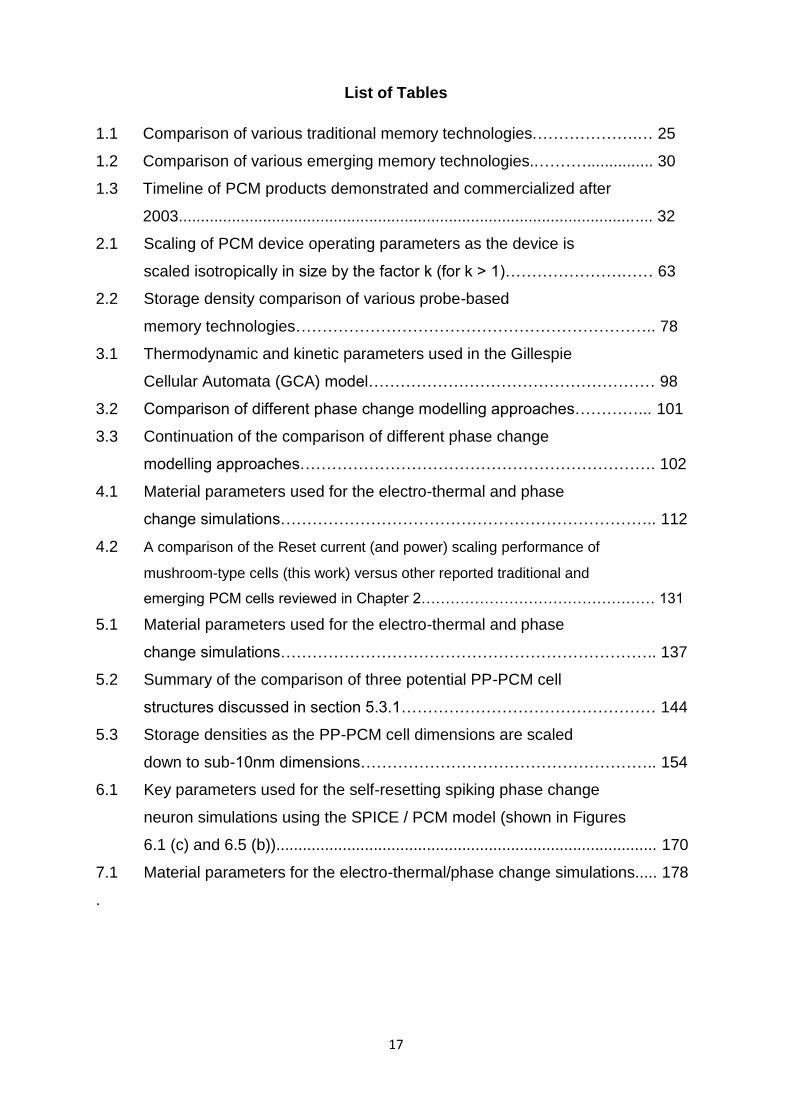
List of Tables
1.1 Comparison of various traditional memory technologies.……………….… 25
1.2 Comparison of various emerging memory technologies..………............... 30
1.3 Timeline of PCM products demonstrated and commercialized after
2003........................................................................................................... 32
2.1 Scaling of PCM device operating parameters as the device is
scaled isotropically in size by the factor k (for k > 1)………………….…… 63
2.2 Storage density comparison of various probe-based
memory technologies………………………………………………………….. 78
3.1 Thermodynamic and kinetic parameters used in the Gillespie
Cellular Automata (GCA) model……………………………………………… 98
3.2 Comparison of different phase change modelling approaches…………... 101
3.3 Continuation of the comparison of different phase change
modelling approaches…………………………………………………………. 102
4.1 Material parameters used for the electro-thermal and phase
change simulations…………………………………………………………….. 112
4.2 A comparison of the Reset current (and power) scaling performance of
mushroom-type cells (this work) versus other reported traditional and
emerging PCM cells reviewed in Chapter 2………………………………………… 131
5.1 Material parameters used for the electro-thermal and phase
change simulations…………………………………………………………….. 137
5.2 Summary of the comparison of three potential PP-PCM cell
structures discussed in section 5.3.1………………………………………… 144
5.3 Storage densities as the PP-PCM cell dimensions are scaled
down to sub-10nm dimensions……………………………………………….. 154
6.1 Key parameters used for the self-resetting spiking phase change
neuron simulations using the SPICE / PCM model (shown in Figures
6.1 (c) and 6.5 (b))...................................................................................... 170
7.1 Material parameters for the electro-thermal/phase change simulations..... 178
.

18
Acknowledgements
First and foremost, I am heartily thankful to my beloved parents Dr. Nabeel and Dr.
Tanzila, and siblings Usama, Sabah and Sarah. Words cannot express how grateful
I am for the endless love, support, and sacrifices they have made throughout my
education and professional career, and I will be forever grateful for their presence in
my life through thick and thin.
I would like to express my deepest gratitude to my PhD Supervisors, Prof. C. David
Wright (University of Exeter, UK) and Dr. Krisztian Kohary (Obuda University,
Hungary) for giving me the opportunity to work on this very exciting PhD project, and
for their guidance, support, enthusiasm and patience. I am sincerely grateful to them
for making my PhD journey a great learning and fulfilling experience.
The present and past members of Prof. Wright’s group have contributed immensely
to my personal and professional time at Exeter. The group has been a source of
friendships, as well as help, advice and collaboration, and I look forward to working
with them in the future. I would like to thank Dr. Karthik Nagareddy, Dr. Arseny
Alexeev and Toby Bachmann for helpful discussions regarding COMSOL modelling,
experimental work and publications. I would also like to thank Prof. Gino Hrkac for
his advice and support as a mentor throughout the last 3 years. With regards to the
research on neuromorphic computing and phase change metadevices in this thesis, I
would also like to acknowledge fellow group members Dr. Rosie Cobley for the
SPICE simulations in Chapter 6, and Santiago Garcia-Cuevas Carrillo for the
modulator reflectance simulations in Chapter 7.
Last but not least, a special thanks to all my dear friends here in Exeter, in other
parts of the UK and abroad, for the moral support, motivation, and the great
memories we have shared. I am blessed to have friends like them in my life and the
completion of this thesis would not have been possible without them.
Yours Sincerely,
Hasan

19
Chapter 1 Introduction and Motivation
Digital data, obtained from the digitization of various forms of information such as
text, image or voice, and sound, plays a vital role in different aspects of our daily
lives including business, education, entertainment and communication. The last few
decades have seen an extraordinary shift in the usage and value of data storage and
memory technologies, driven mainly by the advancements of three particular
applications. The first and most significant shift has been the increased usage of
modern electronic devices, such as tablets and mobile phones. The second trend
has been the shift of focus from individual electronic components to the ability to
integrate an increasingly larger volume of elements into subsystems rather than as
discrete components on a processor. The third trend has been the increase in the
amount of information created and reproduced in digital form, which surpassed the
Zettabyte barrier in 2010 [1, 2], and is predicted to increase up to 40 Zettabytes by
2020 [1] (the equivalent of 5200 Gigabytes (GB) per human being), as shown in
Figure 1.1. This exponential increase in digital data can be fathomed by the fact that
the total storage of personal information uploaded by users to the Facebook server
by the end of 2014 exceeded 500 Petabytes. At the same time Google handled
more than 7300 Petabytes during that year alone [3, 11].
Figure 1.1 The growth rate of global digital data per year (adapted from Ref. [1]).

20
1.1 Overview of Data Storage and Memory Technologies
Today’s electronic and computing systems use a hierarchy of data storage devices
to achieve an optimal trade-off between cost and performance. These devices can
be divided into two main categories: (1) volatile memories, and (2) non-volatile
memories, as shown in the memory taxonomy in Figure 1.2. In volatile memories,
the conservation of data with time (data retention) requires a constant power supply
(SRAM, Static Random Access Memory) or periodical refreshing (DRAM, Dynamic
Random Access Memory), both of which can be costly in terms of energy, and are
consequently expensive. However, volatile memories have very short execution
times (~μs-ns), and are used to complete the main tasks in the central processing
unit (CPU) such as logic operations [4]. On the other hand, non-volatile memories
such as Flash memories and Hard Disk Drives (HDDs) retain data even when the
power supply is turned off. These memories have slower processing times, and
hence are used mainly for data storage purposes [4]. Section 1.1.1 discusses the
characteristics and limitations of some of the currently used volatile and non-volatile
memories in further detail.
Figure 1.2 Memory taxonomy showing various Traditional and Emerging Memory
Technologies (adapted from the International Technology Roadmap for
Semiconductors (ITRS) 2013 [7]).
Memory Technologies
Non-volatile Volatile
SRAM
DRAM Flash
NAND & NOR
MRAM
ReRAM
PCM
FeRAM
Emerging Traditional
HDD
Traditional

21
1.1.1 Traditional Memory Technologies
The general technology requirements of memories in modern computing systems
are size scalability, high storage density, high endurance, fast speed, low power
consumption, low cost, and compatibility and integration with the complementary
metal oxide semiconductor (CMOS) platform [5]. For decades, SRAM and DRAM
(volatile), and Flash and HDD (non-volatile) have been the workhorses of the
memory hierarchy (shown in Figure 1.3 (a)), and hence are classified as traditional
(or established) memory technologies.
1.1.1.1 Static Random Access Memory (SRAM)
SRAM gains its name from the fact that data is held in a ‘static’ manner, and does
not need to be dynamically refreshed (updated) as in the case of DRAM (Section
1.1.1.2). It is also ‘random’ which means individual bits in the memory can be
accessed rather than being processed sequentially. Whilst the data in SRAM
memory does not need dynamic refreshing (making it faster than DRAM), it is still
volatile, and as a result data is not held when the power supply is turned off.
The SRAM memory cell typically consists of four transistors configured as two cross
coupled inverters, and has two stable states equating to logical ‘1’ and ‘0’ states. In
addition to the four transistors, an additional two transistors are also required to
control access to the memory cell during read and write processes making a total of
six transistors, hence termed as a 6T memory cell (circuitry shown in Figure 1.3 (b)).
At present, SRAMs in computer systems are embedded within the CPU and act as
Level 1 (L1) and Level 2 (L2) cache memories [6].
Despite SRAM being a well established technology, its (1) large cell size (due to the
6 transistors translating to an 84F2 size, with F being the smallest feature possible
with a chosen lithography technology), and (2) high energy consumption (due to the
requirement of a constant power supply) are major limiting factors in the
development of this technology. At present it is not clear whether scaling beyond the
16nm node will be possible at all in SRAM [7], hence new alternative memory
technologies will be required in order for memories to further scale down to smaller
(sub-10nm) dimensions.

22
1.1.1.2 Dynamic Random Access Memory (DRAM)
DRAM stores each data bit on a capacitor within the memory cell which is
consistently charged and discharged to provide logical ‘1’ and ‘0’ states. Due to
charge leakage of the capacitor, it is necessary to refresh the memory cell
periodically, which gives rise to the term ‘dynamic’. In contrast, SRAMs do not have
to be refreshed. However, DRAM is also volatile, and data is not held when the
power supply is disconnected.
DRAM cells consist of one capacitor and one transistor (shown in Figure 1.3 (c)),
where the capacitor is used to store charge, and the transistor acts as a switch which
enables the control circuitry on the memory chip to read the capacitor or change its
state. One of the advantages of DRAM over SRAM is the simplicity of the cell i.e. in
DRAMs a single transistor is required for its operation in comparison to SRAMs
which require 6 transistors, making its cell size much smaller (6F2). This simplicity
also means lower production costs and higher storage densities [9]. However,
constant refresh cycles required for the recharging of the capacitor leads to extra
power consumption, and processing speeds slower than those in SRAMs. Similar to
SRAM, it is not clear whether DRAM cells of the future will be scalable beyond the
16nm node [7], affirming the need for alternative memory technologies which can
scale down to single nanometer dimensions.
1.1.1.3 Flash Memory
Flash memory was first developed by Toshiba in 1980 and is currently the most
widely used technology for electronic non-volatile storage. A typical Flash memory
cell (shown in Figure 1.3 (d)) consists of a storage transistor with a control gate and
a floating gate. A thin dielectric material or oxide layer is used to insulate the floating
gate from the rest of the transistor, and is responsible for storing electrical charge
and controlling the flow of current. The transfer of charge (electrons) comes from
Fowler- Nordheim tunnelling (a process in which electrons tunnel through a barrier in
the presence of a high electric field), or hot electron injection (a process in which an
electron gains sufficient kinetic energy to overcome a barrier necessary to break an
interface state) which traps the charge in the floating gate, and once stored, charge

23
(a)
(b) (c) (d)
(e)
Figure 1.3 (a) Physical distribution and hierarchy of memory in a computer (reprinted
from [8]), (b) Schematic of a circuit of a SRAM cell consisting of six transistors. BL,
bit line; , logic complement of BL; WL, word line; VDD, supply voltage (reprinted
from [8]), (c-d) Schematics of DRAM and Flash memories (reprinted from [8]), (e)
Schematic of a typical hard disk (reprinted from [12]).

24
can remain stored at detectable levels for up to 10 years. As the floating gate is
surrounded by an insulator, no refresh cycles are needed as in the case of DRAM
[4]. Flash memory is further divided into two main categories: (1) NOR Flash, which
uses no shared components and enables random access to data by connecting
individual memory cells in parallel, and (2) NAND Flash, which is more compact in
size, with a lesser number of bit lines, and connects floating-gate transistors together
to achieve greater storage. Hence, NAND Flash is better suited to serial data,
whereas NOR Flash is better suited to random access data [4].
Flash memories can be seen in many forms today such as USB memory sticks,
digital camera memory cards in the form of Compact Flash, SD cards, mobile
phones, laptops, tablets, MP3 players and many more. In comparison to SRAM and
DRAM, Flash is much cheaper, retains data even when the power supply is
disconnected (non-volatility), and has storage capacities now exceeding Terabytes
on a single drive. However, similar to SRAM and DRAM, Flash suffers from some
fundamental drawbacks that limit its future potential. In particular, as the technology
node continues to scale down, the tunnelling of charge from the floating gate, leading
to data loss, becomes a significant problem, and as the cell density increases, the
parasitic effect [10] of one cell on adjacent cells becomes prominent. Hence, scaling
Flash memories beyond 16nm will be exceedingly difficult without a significant
increase in manufacturing costs [4]. In addition, Flash has much slower writing
speed (μs–ms) and a seriously limited endurance (~104-5 cycles) [11]. Hence, an
alternative memory technology, free from scaling issues with non-volatile data
retention, is very much desired.
1.1.1.4 Limitations of Traditional Memory Technologies
The characteristics and limitations of the three main volatile and non-volatile
memories in use today (SRAM, DRAM and Flash) have been discussed in Sections
1.1.1.1 – 1.1.1.3. In addition to these technologies, the other main non-volatile
storage technology is HDD (Hard Disk Drives, in which reversible magnetic
microdomains are created and erased for data storage (shown in Figure 1.3 (e)).
The limitations of various traditional memory technologies are listed below and their
operational characteristics are summarized in Table 1.1.

25
SRAMs and DRAMs are volatile memory technologies; hence a constant power
supply or constant refreshing is required for data retention leading to an increase
in power consumption. In addition, SRAM and DRAM cells are large in size, and
scaling beyond 16nm is challenging for both SRAM and DRAM.
Flash memories have higher storage capacities, are cheaper, and are non-
volatile; therefore no refresh cycles or constant power supply is needed.
However, Flash memories are slower (μs–ms), have limited endurance (~104-5
cycles), and it is challenging to scale them down to sub-10nm dimensions at
present.
HDDs are non-volatile and have been in use since the 1950s. However, they
are much larger in size, slow, and can suffer from head ‘crashes’ which damage
the disk surface resulting in loss of data in that sector.
Table 1.1 Comparison of various traditional memory technologies [4, 7, 13].
SRAM DRAM Flash HDD
Cell Area (F2) 80-140 6-12 4 2/3
Non-volatility No No Yes Yes
Endurance (cycles) 1016
1016
104-5
104-5
Energy per bit (pJ) 5 x 10⁻⁴
5 x 10⁻³
2 x 10⁻⁴
5 x 10³-4
Speed <1ns 10ns 1-10ms 5-8 ms
Retention as long as V
applied
<<seconds years years
The limitations and challenges summarized above have led researchers to develop
alternative (emerging) non-volatile memory technologies that are relatively free from
scaling issues, have lower power consumptions, higher storage densities, faster
speeds, can be easily integrated on-chip with the microprocessor cores, and store
information using new types of physics that do not rely on storing charge on a
capacitor like in DRAM and Flash [8, 9, 11]. Section 1.1.2 discusses some of these
emerging memory technologies in further detail.

26
1.1.2 Emerging Memory Technologies
In recent years, emerging memory technologies (shown in Figure 1.2) such as
Ferroelectric RAM (FeRAM), Magnetic RAM (MRAM), Resistive RAM (RRAM), and
Phase Change Memory (PCM) have been proposed to complement or even replace
in some environments, the traditional memory technologies discussed in Section
1.1.1. These emerging technologies are also termed as “universal” memory
technologies, where the term “universal” generally refers to technologies that can
substitute both primary (SRAM and DRAM), and secondary (Flash and HDD)
technologies without losing any of their respective advantages. The following
sections discuss and compare the characteristics of some of the leading emerging
technologies in use today.
1.1.2.1 Ferroelectric RAM (FeRAM)
FeRAM is a type of non-volatile memory based on the permanent polarization of a
ferroelectric material (a material that exhibits, over some range of temperature, a
spontaneous electric polarization which can be reversed or reoriented by applying an
electric field), and has a similar one-transistor/one-capacitor cell structure to DRAM
(shown in Figure 1.4). However, the capacitor typically uses a ferroelectric material
such as PZT (PbxZr1-xTiO3) as the dielectric layer [13], and when charged or
discharged (logical ‘0’ and ‘1’ states), a polarization is encoded in the material
caused by the change in the positions of the atoms under the application of an
electric field. A read is performed by forcing the cell into a particular (known) state,
and depending on the polarization of the ferroelectric material, a current spike occurs
on the output terminal, allowing the prior polarization to be determined.
FeRAMs have considerable advantages over DRAM and Flash, such as lower power
consumption, faster write speeds and no need for constant refresh cycles [4].
However, scalability of FeRAMs is a major drawback at present, mainly due to the
signal being proportional to the area of the ferroelectric capacitor, and inversely
proportional to thickness, which is limited in scaling by the interaction of the
ferroelectric material with the electrodes, hence giving rise to a ‘dead zone’ [13]. In
addition, limited endurance, an intrinsically large cell size, and data loss during the
read operation, are all limiting factors in the development of FeRAMs. To overcome

27
Figure 1.4 FeRAM schematic cross-section (left) (reprinted from [13]), and
FeRAM basic working principle (right) showing that the ferroelectric capacitor can be
polarised either up or down by applying the relevant electric field.
these challenges, Ferroelectric Field Effect Transistors (Fe-FETs) and Ferroelectric
Polarization RAMs (Fe-PRAMs) have been proposed as potential solutions [13, 14].
In addition, SBT (SrB2Ta2O9) has also been proposed as a replacement for the more
widely used PZT material to improve scalability [11]. Despite FeRAMs being trialled
in automobile equipment, railway passes, and other electronic appliances in recent
years [15], further research on the mentioned limitations is required before FeRAMs
can become a dominant and more commercially-viable memory technology.
1.1.2.2 Magnetic RAM (MRAM) and Spin Torque Transfer MRAM (STT-MRAM)
MRAM, first developed by IBM in the 1970s [16], is a form of non-volatile memory
that uses magnetic charge to store data instead of electric charge used in DRAM
and SRAM technologies. The basic cell structure of MRAM is based on a magnetic
tunnel junction (MTJ) which consists of a conducting layer sandwiched between two
ferromagnetic layers, with one layer having a fixed magnetization, and the other
being a free layer (with a weak coercive field) which can be switched. Data bits are
stored as the orientation of the magnetism in the variable layer, and are read from
the cell resistivity. When the two layers are parallel, electrons with opposite spin
pass without any hindrance allowing the flow of current, resulting in a low resistance
ON state (logical ‘1’). On the other hand, when the layers are not parallel, electrons
are scattered strongly, resulting in a high resistance OFF state (logical ‘0’), as shown
in Figure 1.5 (a).

28
(a) (b)
Figure 1.5 (a) Basic functioning of MRAM (reprinted from [13]). (b) Conventional
MRAM device structure vs STT-RAM device structure (Reprinted from [18]).
MRAM magnetic memories present considerable advantages over traditional
memory technologies, such as fast speeds (<20ns) and high endurance cycles
(>1012 cycles) along with non-volatility [4, 9]. However, MRAMs at present have a
small ON/OFF current ratio (in the order of 30%), high programming currents,
complex structure for fabrication, and problems with write operations disturbing
neighbouring cells which limit the storage density [13, 14]. Also, similar to FeRAMs,
MRAMs have a serious handicap in terms of scaling due to the fact that a
degradation of the write, read and retention properties is observed, which is due to
the thermal instability of the magnetization in the free (weak coercive field) layer [4].
To overcome the limitations of conventional MRAMs, several improvements have
been proposed, such as the introduction of Magnesium Oxide (MgO) as a dielectric
material (which was shown to increase the ON/OFF current ratio by more than 300%
[13]), and the invention of STT-MRAMs (Spin Torque Transfer MRAMs, cell structure
shown in Figure 1.5 (b)) as a potential replacement for existing memory
technologies. STT-MRAMs exploit the spin torque transfer phenomenon of magnetic
materials (an electromagnetic effect that makes it possible to reverse the
magnetization by using spin-polarized electric current), and in comparison to
conventional MRAMs, have shown lower switching currents (~μA), faster speeds
(~tens of ns), and better scalability (6F2) [11]. In addition, an industrial prototype of
1Gb STT-MRAM at the 54nm node (14F2) has also been presented by Hynix
Semiconductor [17].

29
1.1.2.3 Resistive RAM (RRAM)
RRAMs are non-volatile memories that store data via the electrical switching
between distinct resistance states observed in numerous metal oxides (such as
NiOx, TiOx, and TaOx). A typical RRAM cell consists of a resistance-changeable
material sandwiched between two metal electrodes, and the change in resistance is
achieved by applying controlled current or voltage pulses between the electrodes
which typically forms a conductive filament (as shown in Figure 1.6 (a)). The
transition from a high resistance OFF state to a low resistance ON state (Set
process, Figure 1.6 (b), left), and the reverse transformation from the low resistance
ON state to high resistance OFF state (Reset process, Figure 1.6 (b), right) are
obtained using different voltage polarities. If the polarities of the Reset and Set
states are of the same sign, the RRAM system is termed as ‘unipolar’, and if the
polarities are of the opposite sign, the system is ‘bipolar’.
Oxide-based RRAMs are currently one of the most competitive candidates for future
non-volatile memory applications due to their simple cell structure, fast switching
speeds (~10ns), compatibility with CMOS, and good scalability (<30nm) [19, 20]. In
addition, further variations of RRAMs such as CBRAM (Conductive Bridge RAM, a
type of RRAM which uses a reactive electrode that supplies mobile ions (e.g. Cu+,
(a) (b)
Figure 1.6 (a) Schematic of a RRAM cell with insulator (or semiconductor)
sandwiched between metal electrodes. (b) RRAM switching mechanism showing the
transition between a low resistance ON state, and high resistance OFF state
(reprinted from [9]).

30
Ag+) to move through insulating dielectrics (known as solid-state electrolytes) to form
conducting filaments in the ON state) have demonstrated a large ON/OFF ratio, fast
speed, and long endurance [14], along with a 16Gb CBRAM test chip presented
recently [21]. However, a major challenge in oxide-based RRAMs at present is
reliability, mainly variability and failure. In RRAMs the switching (formation and
rupture of filaments) is not controlled microscopically, and is intrinsically stochastic,
which is reflected in a large variation of device resistance and switching voltage from
cycle to cycle and device to device [14]. In addition, the failure mechanisms in
RRAMs are not well understood at present. Hence, further research is required to
address reliability and power consumption challenges before RRAMs can become a
leading memory technology of the future [14, 20].
Table 1.2 Comparison of various emerging memory technologies [4, 9, 19, 22].
FeRAM MRAM STT-MRAM RRAM PCM
Cell size (F2) 20-40 25 6 4 4
Storage
Mechanism
Permanent
polarization of
a ferroelectric
material (PZT
or SBT)
Permanent
magnetization
of a
ferromagnetic
material in a
MTJ
Spin-
polarized
current
applies
torque on a
magnetic
moment
Switching
between
High/Low
Resistance
states of
metal oxide
materials
Switching
between
Amorphous
/Crystalline
states of
phase change
materials
Non-volatility Yes Yes Yes Yes Yes
Endurance 1012
cycles >1012
cycles >1014
cycles >1010
cycles >1010
cycles
Speed (ns) <100ns <20ns <10ns <10ns <10ns
Power
Consumption
Average Average to
High
Low Low to
Average
Low
Maturity Limited
Production
Test chips Test chips Test chips Test chips
Cost ($/Gb) High High High Very High Average
Applications Low Density Low Density High Density High Density High Density

31
1.1.2.4 Summary of Emerging Memory Technologies
In sections 1.1.2.1 – 1.1.2.3 the characteristics of some of the leading emerging
memory technologies have been discussed along with their key attributes and
features summarized in Table 1.2. In addition to the discussed technologies, other
new contenders such as Carbon-based memories, Mott memories, Molecular and
Macromolecular memories, Polymer memories, and NEMS memories are also being
studied intensively at present to determine their viability as potential replacements
for existing traditional memory technologies.
For the remainder of this thesis, the main focus is on Phase Change Memory (PCM),
(also referred to as Phase Change Random Access Memory (PCRAM)), which is a
type of non-volatile memory that relies on the fast and reversible switching of phase
change materials (glass-like materials, also known as chalcogenides) between a
high resistance amorphous state and low resistance crystalline state for the storage
of data, and is one of the leading contenders to complement or even replace the
existing traditional memory technologies discussed in section 1.1.1. Table 1.2 also
shows that it has some of the best performance features in comparison to other
emerging memory technologies discussed in section 1.1.2. The following sections
1.2 – 1.4 of this chapter discuss the characteristics and key features of PCM and
phase change materials in further detail.
1.2 Phase Change Memory (PCM)
1.2.1 Background and Commercialization of PCM
The origins of PCM trace back to the pioneering work of Stanford Ovshinsky on the
physics of amorphous solids in the late 1960s when he proposed that chalcogenide
glasses (alloys consisting of elements from the chalcogen family e.g. Selenium,
Tellurium, etc) exhibited two different resistive states, and could be reversibly
switched between these two states, using an electrical pulse, to form solid state
memory devices [23]. Following Ovshinsky’s work, the first 256 bit PCM array was
demonstrated in 1970 by R. G. Neale, D. L. Nelson and Gordon Moore [24]. This
memory cell consisted of a PCM storage element aligned in series with a silicon
based p-n diode as an access device. Later in 1978, the first prototype of a 1024 bit
PCM was demonstrated by Burroughs Corporation [25]. Despite this promising start

32
in PCM research, high power consumptions related to large device sizes and slow
crystallization times (in the μs – ms range [26]) prevented PCM products from being
commercialized, and for almost a decade, research on PCM was largely abandoned.
However, this changed with the discovery of fast switching alloys by Yamada et al in
1987 [27]. These alloys showed a large optical contrast over a wide range of
wavelengths, good cyclability, in addition to short crystallization times, and played a
leading role in the commercialization of PCM in the years to follow.
The discovery of fast switching alloys in 1987 allowed for the first commercial
application of a 500MB optical disk by Panasonic Corp. in 1990, and later the CD-
RW in 1997, DVD-RW in 1999, and the Blu-ray disk in 2003 [28]. Most of these
products employ phase change materials (specifically GeTe-Sb2Te3 materials based
on the pseudobinary line, see Figure 1.10 (a) and section 1.3). Following these
inventions, numerous companies, such as Samsung, Intel, IBM, Numonyx, and
STMicroelectronics (to name a few) started research into electrical switching of
phase change materials and began PCM development programs in the early 2000s.
A timeline of some of the prominent PCM products demonstrated by various
companies since 2003 is shown in Table 1.3.
Table 1.3 Timeline of PCM products demonstrated and commercialized after 2003.
PCM Product Company Year
64 Mbit PCM array Samsung August 2004
256 Mbit PCM array Samsung September 2005
512 Mbit PCM device Samsung September 2006 (Mass
production in September 2009)
128 Mbit PCM chip Intel and ST Microelectronics October 2006
128 Mbit PCM device Numonyx December 2008
1Gb 45nm PCM device Numonyx December 2009
512 Mbit PCM with 65nm Samsung April 2010
8Gb 1.8V PCM with 20nm Samsung February 2012
PCM (combining Flash and
DRAM) on a single controller
IBM May 2014
3D Xpoint memory employing
PCM as storage element
Intel and Micron July 2015

33
1.2.2 Phase Change Memory (PCM): Operation Principle
PCM relies on the fast and reversible electrical switching of phase change materials
(glass-like materials, also known as chalcogenides) between two different states: a
disorderly amorphous phase (short range atomic order), and an orderly crystalline
phase (long range atomic order) [29]. The transition from the crystalline phase to the
amorphous phase is commonly known as the Reset process, and the transition from
the amorphous phase to the crystalline state is known as the Set process. The
amorphous phase is characterized by a high electrical resistance and low optical
reflectivity (corresponding to a logical ‘0’), whereas the crystalline phase is
characterized by a low electrical resistance and high optical reflectivity
(corresponding to a logical ‘1’), and it is this contrast between the two distinct phases
that enables the storage of data in PCM.
A typical PCM cell used for electrical switching (known as the mushroom cell, shown
in Figure 1.7 (a)), consists of the active phase change material sandwiched between
a top metal electrode, and a metal heater, which in turn, is connected to a bottom
metal electrode. The phase transitions are achieved by means of electrical pulses
though the heater, resulting in Joule heating (a process by which the passage of
electric current through a conductor releases heat) in the phase change material.
(a) (b)
Figure 1.7 (a) Schematic of a typical PCM ‘mushroom’ cell. (b) Reversible switching
in PCM between an ‘orderly’ crystalline phase, and ‘disorderly’ amorphous phase
using Set and Reset pulses respectively.
Top metal electrode
Bottom metal electrode
Phase change material
Active
Region
Heater
Thermal
Insulator
Crystalline Amorphous Crystalline Amorphous
Crystalline Amorphous
‘0’ ‘1’
Crystalline Amorphous
‘0’ ‘1’
Reset
Set
Crystalline Amorphous
‘0’ ‘1’
Reset
Set

34
Figure 1.8 Typical current - voltage (I-V) curve for a PCM cell showing the
threshold voltage (Vth). SET and RESET denote the switching regions, while READ
denotes the region of data readout (Reprinted from [31]).
As shown in Figure 1.7 (b), amorphization is achieved by applying a high power,
short duration electrical pulse (Reset pulse) to heat the material up to its melting
temperature, Tm, followed by rapid cooling (quenching) that freezes the material into
its amorphous state. Crystallization is achieved by applying a lower amplitude, longer
duration electrical pulse (Set pulse) which raises the temperature in the amorphous
active volume to above crystallization temperature, Tx, but below the melting
temperature, allowing for the formation of the crystalline phase [30]. A low power
pulse is then used to retrieve the data by sensing the cell’s resistance (with the
amplitude of this pulse being too low to induce any phase change). The electrical
resistance between the low-conducting amorphous and high-conducting crystalline
phases typically differs by 1-3 and up to 5 orders of magnitude.
1.2.3 Threshold Switching
The operation of PCM also depends on a threshold effect during electrical switching,
which is commonly known as ‘threshold switching’. Figure 1.8 shows a typical
current-voltage (I-V) curve of the Reset and Set state of a PCM cell. The I-V curve
for the Reset (amorphous) state shows a very high resistance (~MΩ) for small
currents (OFF state) until a specific threshold voltage, Vth, is reached, after which a
Vth

35
‘snap back’ takes place, and the cell switches from the highly resistive OFF state to a
conductive ON state. This ON state is characterized by a relatively small resistance
(~kΩ), and hence, a large current can flow (for moderate applied voltages). The
threshold switching effect plays a crucial role in phase change switching, as it allows
a high current density in the amorphous state without having to apply high amplitude
pulses. Without this mechanism, which allows large currents to flow in a resistive
amorphous material at low voltages (~typically less than 5V), a high voltage
(~greater than 100V) would be required for switching, hence making the phase
change process effectively unfeasible [32].
1.2.4 PCM Device Structures and Scaling Characteristics
The fundamental design strategy for PCM is to develop cell structures that can
physically restrict the current flow through the cell to a small ‘passage’. As the size
of this passage decreases, so does the volume of the material being used for
switching by melt quenching into an amorphous phase during the Reset process. As
a result of a reduction in the switching volume, the current (and hence power)
requirements decrease (and switching speeds increase), and so a key challenge is
to be able to define cell structures with appropriately constrained/physically defined
nanoscale switching regions. However, due to lithographic and material restrictions,
there are both technological and fundamental limits on how small PCM devices can
be made and still function effectively. To tackle these challenges various device
structures have been proposed in the literature, which can be divided into two main
categories: (1) ‘Traditional’ cell structures such as the mushroom, μTrench, dash,
pore, crossbar and probe-based cells, and (2) ‘Emerging’ device structures such as
nanotube-based cells, nanowires, lateral and bridge cells, nanoclusters and
nanoparticles, superlattice-like (SLL) cells, and graphene-based cells, as shown in
Figure 1.9.
A detailed review of the operation mechanisms, and in particular, scaling
characteristics of some of the key PCM cell structures (mentioned above) has been
presented in Chapter 2 of this thesis.
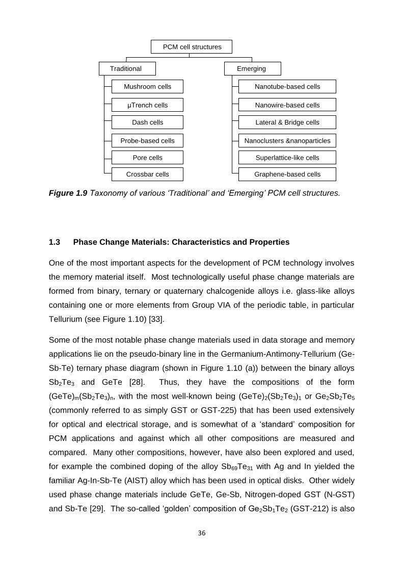
36
Figure 1.9 Taxonomy of various ‘Traditional’ and ‘Emerging’ PCM cell structures.
1.3 Phase Change Materials: Characteristics and Properties
One of the most important aspects for the development of PCM technology involves
the memory material itself. Most technologically useful phase change materials are
formed from binary, ternary or quaternary chalcogenide alloys i.e. glass-like alloys
containing one or more elements from Group VIA of the periodic table, in particular
Tellurium (see Figure 1.10) [33].
Some of the most notable phase change materials used in data storage and memory
applications lie on the pseudo-binary line in the Germanium-Antimony-Tellurium (Ge-
Sb-Te) ternary phase diagram (shown in Figure 1.10 (a)) between the binary alloys
Sb2Te3 and GeTe [28]. Thus, they have the compositions of the form
(GeTe)m(Sb2Te3)n, with the most well-known being (GeTe)2(Sb2Te3)1 or Ge2Sb2Te5
(commonly referred to as simply GST or GST-225) that has been used extensively
for optical and electrical storage, and is somewhat of a ‘standard’ composition for
PCM applications and against which all other compositions are measured and
compared. Many other compositions, however, have also been explored and used,
for example the combined doping of the alloy Sb69Te31 with Ag and In yielded the
familiar Ag-In-Sb-Te (AIST) alloy which has been used in optical disks. Other widely
used phase change materials include GeTe, Ge-Sb, Nitrogen-doped GST (N-GST)
and Sb-Te [29]. The so-called ‘golden’ composition of Ge2Sb1Te2 (GST-212) is also
PCM cell structures
Nanotube-based cells
Lateral & Bridge cells
Nanoclusters &nanoparticles
Superlattice-like cells
Nanowire-based cells
Emerging Traditional
Mushroom cells
μTrench cells
Dash cells
Probe-based cells
Pore cells
Crossbar cells Graphene-based cells

37
gaining traction due to its impressive properties when compared to other established
phase change materials [34]. Another notable material development includes
Gallium-Lanthanum-Sulphide (commonly referred to as GLS) which has also
exhibited impressive properties such as high thermal stability, high electrical
resistivity in both amorphous and crystalline phases, large contrast between the two
phases, and potential for low power and fast switching at the nanoscale [35, 36, 37].
(a) (b)
Figure 1.10 (a) The ternary Ge-Sb-Te phase diagram with some popular phase
change alloys highlighted (the red arrow indicates the trend of adding Ge to the so-
called ‘golden’ composition Ge2Sb1Te2 alloy). (b) A map of Te-based phase change
materials as a function of material ionicity and hybridization (Reprinted from [38]).
1.3.1 Key Features of Phase Change Materials
Some of the remarkable features that make phase change materials well suited for
modern data storage, memory and computing applications can be summarized as
follows.
They exhibit huge differences, up to five orders of magnitude, in electrical
resistances between phases

38
They can be switched between phases with low current (<10μA)
They can be switched between phases at very fast speeds (ns-ps)
They remain stable against spontaneous crystallization for many (>10) years
They exhibit large differences in refractive index between phases
They can be cycled between phases up to 1012 times
1.3.2 Key Properties of Phase Change Materials
As discussed in sections 1.2 and 1.3 so far, phase change materials exhibit different
properties in the crystalline and amorphous phases. Some of these key properties
have been listed below:
crystallization temperature, Tx, and amorphization (melting) temperature, Tm
crystal nucleation and growth
activation energy, Ea, for phase transformation
electrical and thermal properties such as conductivity and resistivity
variation in resistance levels
Detailed discussions on the key properties listed above have been presented over
the course of this thesis.
1.3.3 Scaling of Phase Change Materials
The fundamental question regarding the scalability of PCM is whether the
programmable region consisting of the phase change material can switch between
the amorphous and crystalline phases rapidly and repeatedly when the dimensions
are reduced to the ultimate scaling sub-10nm region, even perhaps as we approach
the atomic limit. Although it is well known that phase change materials exhibit
different properties at the nanoscale in comparison to bulk, it is vital to know how the
reduction in size influences the key material properties listed in the previous section
1.3.2. To study and understand how these properties vary with reduction in size,
scaling can typically be performed in one-, two-, and three-dimensions.
A detailed review of the scaling characteristics of phase change materials using the
three mentioned scaling mechanisms has been presented in Chapter 2 of this thesis.

39
1.4 Advanced Functionalities of Phase Change Materials & Memory Devices
The ability to switch a phase change material between different states not only
enables memory storage, but also opens the opportunity for more advanced
applications that go beyond two-level memory cells. Some of these applications are
introduced briefly in the following subsections 1.4.1 - 1.4.3.
1.4.1 Neuromorphic (Brain-inspired) Computing
A novel application of phase change materials, which utilizes the progressive
changes in resistance, is to mimic the behaviour of biological synapses (junction
between two nerve cells where impulses are transmitted and received). This is often
referred to as ‘neuromorphic’ or ‘brain-inspired’ computing. Kuzum et al [39] used a
system of connected phase change memory cells (using GST) in a crossbar
structure (see section 2.2.4) to develop a hardware implementation of the Hebbian
learning scheme [40], which models changes in the connection strength of synapses
based on the timing difference between activity ‘spikes’ on the connected neurons.
Figure 1.11 shows the interconnection scheme of PCM synapses to reach ultrahigh
density and compactness of the brain. In the crossbar array shown, PCM synapses
lie between postspike and prespike electrodes, inspired by biological synapses
formed between presynaptic and postsynaptic neurons. Cross-sections of
depressed (mushroom shaped amorphous regions (red in colour)) and potentiated
synapses have also been shown. The system presented by Kuzum et al was [39]
able to reproduce the learning behaviour of rat neurons, demonstrating the potential
of phase change materials to open up new computing paradigms, which promise
significant gains in efficiency for very complex tasks, which traditional computing
architectures are not ideally suited to accomplish.

40
Figure 1.11 Bioinspired electronic synapses [39]: The interconnection scheme of
PCM synapses to reach ultrahigh density and compactness of the brain is shown. In
the crossbar array, PCM synapses lie between postspike and prespike electrodes,
which are inspired by biological synapses formed between presynaptic and
postsynaptic neurons. Cross-sections of depressed (mushroom shaped amorphous
regions (red)), and potentiated synapses have also been shown (reprinted from [39]).
1.4.2 In-Memory Processing: Beyond von-Neumann Computing
As a second application, Wright et al [41] used mushroom type cells (see section
2.2.1) and probe-based cells (see section 2.2.5), with GST as the phase change
material, to show theoretically (using the GCA algorithm (see section 3.3.5), and
experimentally that the ‘accumulation’ regime can be used to perform not only a
complete range of arithmetic operations (addition, subtraction, multiplication and
division), but also execute complicated non-binary processing and computation,
including parallel factorization and fractional division with phase change cells that
process and store data simultaneously, and at the same location. It was also shown
that the same accumulation property can be used to provide a simple form of phase-

41
change integrate-and-fire “neuron,” which by combining both phase-change synapse
and neuron electronic mimics, potentially offers a range of functionality that goes
beyond simple binary memory to incorporate new forms of phase-change computing.
Figure 1.12 shows Wright et al’s implementation of the base-10 phase change
accumulator, using a GST-based mushroom-type cell, where the input excitation was
designed such that 10 input pulses were required to switch the cell from the Reset to
the Set state. The cell accumulates energy from each input pulse, and eventually
acquires sufficient energy to transform the active region from the amorphous state to
the crystalline state. Figure 1.12 also shows that in state-1 (after the 1st input pulse
is applied), one or two crystal nuclei are formed which have little effect on the cell’s
resistance. After the 5th pulse is applied (state-5) a few more nuclei are formed,
which continue to grow as seen in state-9 (with the cell’s resistance still relatively
high at this point). However, a large decrease in resistance is observed after the 10th
pulse is applied with the amorphous region fully crystallized at state-10, and the cell
resistance well below the chosen percolation threshold of 300 kΩ [41]. Thus, the
information is not stored in different resistance levels, and it does not use the same
scheme as proposed for multi-level PCMs (storage of multiple bits in the same cell)
[42, 43], or for phase change based synaptic-like functionality (discussed in sub-
section 1.4.1).
1.4.3 Phase Change Metamaterials and Metadevices
Metamaterials in general are materials with unusual electromagnetic properties that
are not found in naturally occurring materials. Whilst ‘natural’ materials (for example
glass and diamond) have a positive electrical permittivity, magnetic permeability and
index of refraction, in metamaterials these properties can be made negative and it is
these unusual material properties that can be utilized to achieve tuneable,
switchable, nonlinear and sensing functionalities. This can typically be achieved by
introducing artificial structures in repeating patterns at scales smaller than the
wavelengths of the phenomena they influence [44, 45].

42
Figure 1.12 Schematic of the PCM mushroom cell used by Wright et al [45] for
simulations of the phase-change base-10 accumulator response, the cell resistance
after the input of 10 (1.085V, 60ns) pulses, and the simulated structure of the active
region in state-1, 5, 9 and 10. The dark blue regions are amorphous while
crystallites are shown in various colors (with the red region surrounding the dome
also crystalline). (Reprinted from [41]).
Phase change chalcogenides when incorporated into plasmonic (metamaterial)
resonator structures can lead to the modification of the optical properties in the
environment of the resonator according to the phase state of the chalcogenide
material. This mechanism can thus be utilized to design active devices suited to
tuneable absorbers or electrically and optically controlled (switched) modulators.
Samson et al [37] demonstrated switching by exploiting the frequency shift of a
narrowband Fano resonance mode of a plasmonic planar metamaterial that was
induced by a change in the dielectric properties of an adjacent 200nm thick film of
GLS chalcogenide glass. The transition from the amorphous to the crystalline phase
was electrically stimulated and resulted in a 150nm shift in the near-infrared
resonance, providing transmission modulation with a contrast ratio of 4:1 in a layer of

43
(a) (b)
Figure 1.13 (a) All-optical non-volatile, chalcogenide metamaterial switch reported
by Gholipour et al [46] consisting of a multilayer structure of near- to mid-IR
chalcogenide hybrid metamaterial switches (with their indicative thickness shown in
brackets). Single laser pulse control excitations were used to homogenously convert
a GST nanolayer, hybridized with a photonic metamaterial, repeatedly between
amorphous and crystalline states over areas encompassing up to 12000
metamaterial unit cells (with the electron microscopy images of the amorphous and
crystalline states shown on the bottom right). Such a device can provide for high
contrast transmission and reflection switching of signals at wavelengths close to the
metamaterial source (Reprinted from [46]). (b) Schematic of the phase change
metamaterial absorber structure (top) presented by Cao et al [47] to achieve ultrafast
switching (3.4ns) between the amorphous and crystalline phases. A 40nm thick
GST layer was sandwiched between 40nm Au squares at the top and an 80nm thick
Au layer at the bottom. A side view of the structure is also shown (bottom).
(Reprinted from [47]).

44
sub-wavelength thickness [37]. Gholipour et al demonstrated in [46] that bistable,
optically-induced phase switching using GST can provide a platform for the
engineering of non-volatile metamaterial transmission/reflection modulators (shown
in Figure 1.13 (a)) for near- to mid-infrared wavelengths with thicknesses down to
1/27 of the operating wavelength and active domains as large as 2000 μm2 which
can be switched by single nanosecond pulses [46]. Cao et al [47] also incorporated
GST within a ‘metamaterial perfect absorber’ (MMPA) and demonstrated through
finite element simulations that the temperature of amorphous GST can potentially be
increased from room temperature to greater than 900K in just 3.4ns nanoseconds
with a low light intensity of 0.6mW, owing to the enhanced light absorption through
the strong plasmonic resonances in the absorber. The absorber structure in this
study consisted of an array of 40nm thick gold (Au) squares separated from a
continuous 80nm thick Au film by a 40nm thick GST layer (as shown in Figure 1.13
(b)) [47].
These findings showed that the power requirements for photonic devices can be
lowered based on thermal phase change combined with metamaterial arrays, which
paves the way for the realization of ultrafast photothermally tuneable photonic
devices.
1.5 Project Aim and Contribution to Knowledge
The main focus of this thesis is on the scaling and advanced functionality potential of
phase change memory (PCM) devices, which are based on the repeatable switching
of phase change chalcogenide materials, such as Ge2Sb2Te5 (GST), between a high
resistance amorphous state (binary ‘0’) and low resistance crystalline state (binary
‘1’). The scaling process is essential for the development of PCM as it brings with it
a number of performance benefits, such as lower power consumptions, enhanced
storage densities, faster speeds, and ultimately, a lower cost to the end-user.
Although established traditional memory technologies, such as SRAM, DRAM, HDD
and Flash have been the workhorses of the memory hierarchy for decades, these
technologies have their own scaling limitations i.e. it is now fundamentally
challenging to scale these technologies beyond 16nm dimensions (see section 1.1).
In comparison, PCM has shown excellent scaling capabilities, for example, phase
45
change materials have been shown to switch between the amorphous and crystalline
phases in the sub-10nm region, and PCM devices have been shown to switch
repeatedly between the amorphous and crystalline phases with very low
programming currents (μA), ultrahigh storage densities (Tb/in2), and at fast switching
speeds (~ns-ps), (discussed in detail in Chapter 2). In addition, phase change
memory-type devices have also been used to demonstrate novel functionalities,
such as neuronal and synaptic mimics, arithmetic and logic processing, and all-
photonic memories (discussed in section 1.4).
Despite these advancements, some key questions regarding the scalability and
advanced functionalities of PCM technology still remain unanswered. The work in
this thesis aims to answer these questions (listed below) using a physically realistic
Multiphysics Cellular Automata approach, which combines electro-thermal
simulations with a sophisticated phase change algorithm i.e. the Gillespie Cellular
Automata (GCA) algorithm (which has been described in detail in Chapter 3).
Scaling of Phase Change Memory Materials and Devices:
1) Although PCM devices using more exotic and non-commercially viable cell
designs, such as Carbon-Nanotube based cells, have been shown to electrically
switch repeatedly down to sub-10nm dimensions with low programming currents
and fast switching speeds, can conventional and commercially-viable cell
structures, such as mushroom cells, be potentially scaled down to dimensions
as small as a few nanometers? Furthermore, what effect does this scaling
process have on key device and material aspects such as the kinetics of
amorphization and crystallization, thermal confinement, the resistance window
between Reset and Set states, and most importantly the Reset programming
current/power consumption (which is one of the main limiting factors in the
development of PCM devices)?
2) Can probe-based PCM cells, specifically Patterned Probe PCM (PP-PCM) cells,
operate effectively when scaled down to single nanometer dimensions, and
whether this scaling process can potentially enhance storage densities in
electrically switched probe-based cells to greater than currently reported storage
densities of ~1.5-1.6 Tb/in2? The effects of scaling on key material and device

46
characteristics, such as the amorphization and crystallization kinetics, and the
Reset/Set resistance window in such formats is also currently not well
investigated.
Advanced Functionalities of Phase Change Memory Materials and Devices:
3) Neuromorphic (brain-inspired) computing applications to date have concentrated
primarily on the implementation of phase change synapses. In this regard, can
the accumulation mode of operation of phase change devices (combined with an
external comparator-type circuit) be used to potentially mimic the integrative
properties of a biological neuron, hence delivering a ‘self-resetting spiking phase
change neuron’?
4) Can practicable Phase Change Metadevices (for absorber and modulator
applications, and suited to operation in the technologically important near-
infrared range of the spectrum, specifically here 1550nm) be electrically switched
between the amorphous and crystalline phases repeatedly (to complement
optical switching), thus enhancing their capability as tunable photonic devices?
5) Recent studies have shown that phase change materials, such as GST, exhibit
different activation energies at different crystallization temperatures, thus
providing evidence of non-Arrhenius kinetics of crystallization. In light of these
findings, is a sophisticated phase change model such as our Gillespie Cellular
Automata (GCA) model (used in this thesis) also capable of exhibiting such a
non-Arrhenius behaviour, and if so, what might be the factors causing it to exhibit
such kinetics of crystallization?
1.6 Thesis synopsis
After a review and comparison of various traditional and emerging memory
technologies, the operation mechanism and performance characteristics of
phase change materials and PCM devices, and some advanced
functionalities of phase change materials as presented in Chapter 1, the work
presented in each of the subsequent chapters is as follows:

47
Chapter 2. This chapter presents a detailed review of scaling in phase
change memory materials and devices. The reduction in size of phase
change materials can typically be performed in one-, two-, and three-
dimensions. These three scaling mechanisms have been reviewed in detail in
this chapter. Furthermore, a review of the operation mechanisms and scaling
performance of various PCM device structures has also been presented.
Chapter 3. This chapter presents the details and implementation of a
Multiphysics Cellular Automata approach used for the simulation of phase
change memory materials and devices in Chapters 4, 5, 6, 7 and 8 of this
thesis. This modelling approach consists of the combination of three sub-
models i.e. an electrical model (based on the Laplace equation), thermal
model (based on the heat-transfer equation), and phase change model (the
Gillespie Cellular Automata (GCA) approach).
Chapter 4. In this chapter, the scaling characteristics of conventional
mushroom-type PCM devices are reported for the first time down to single-
nanometer dimensions. Key findings related to amorphization and
crystallization kinetics, the requirement for thermal confinement with scaling,
the resistance window between Reset and Set levels, and programming
currents/power consumptions are presented in detail using a systematic
scaling approach.
Chapter 5. In this chapter, the electrical switching and scaling
characteristics of Patterned Probe-PCM (PP-PCM) cells are presented for the
first time down to single nanometer dimensions using a systematic scaling
approach. It is determined whether ultrahigh storage densities (greater than
currently reported storage densities for electrically switched probe-based cells
of ~1.5 - 1.6 Tb/in2) can be achieved by the scaling of PP-PCM cells.
Furthermore, a comparison with other probe storage technologies, such as
thermomechanical, ferroelectric and magnetic probe storage is also
presented.
Chapter 6. This chapter goes beyond PCM device scaling to present findings
related to Neuromorphic Computing (Brain-inspired Computing), in particular
the design and development of ‘Self-Resetting Spiking Phase Change
Neurons’ using the accumulation mode of operation inherent to phase change
48
materials and memory devices. The Multiphysics Cellular Automata model
(presented in Chapter 3) is combined with an external comparator-type SPICE
circuit model to simulate the characteristics of biological neurons.
Chapter 7. This chapter presents findings for another advanced functionality
of phase change materials i.e. Phase Change Metadevices. The main focus
of this chapter is on the electrical switching of such devices, again using the
modelling approach presented in Chapter 3.
Chapter 8. This chapter uses the Gillespie Cellular Automata (GCA) phase
change model to study the ‘non-Arrhenius kinetics of crystallization’ in
GeSbTe phase change materials. The aim is to determine whether our GCA
model is capable of exhibiting such a non-Arrhenius type behaviour reported
in recent theoretical and experimental studies, and if so, what might be the
factors causing it to exhibit such kinetics of crystallization.
Chapter 9. At the end of the thesis, the main outcomes are summarized in
this chapter. An outlook on future research is also presented.

49
Chapter 2 A Review of Scaling in Phase Change Memory
Materials and Devices
In 1965, Gordon Moore of Intel Corporation predicted that the number of transistors
on an integrated circuit would double approximately every 1.5 to 2 years [48], so
establishing the now well-known ‘Moore’s Law’ and setting a target for the scaling of
silicon-based electronic devices that designers still essentially follow today. The
scaling of silicon-based devices over the years is encapsulated by the historic trend
in the so-called technology node, F, which has units of distance and represents the
typical device half-pitch, i.e. half the distance between identical features in a device
array (see Figure 2.1). The smallest device size at any particular technology node is
thus 4F2 and in Moore’s day, since F was on the order of several micrometres, the
smallest devices occupied hundreds of square microns. By 2016 however, most
state-of-the-art Si devices in production were being manufactured at the 22 nm or 14
nm nodes, giving typical device areas of around 1900 and 800 nm2 respectively. A
move towards the 10 nm and 7 nm nodes around 2017 to 2018 is expected for high-
end chips (so device areas of down to 200 nm2). It is observed that the technology
node, F, typically scales by a factor of 0.7. This means that the device area scales
by a factor of 0.49 = ~0.5, and as a result twice the number of transistors can be
incorporated on the same area. This scaling process in modern electronic devices is
essential due to the following reasons.
If we can double the number of transistors incorporated on the same area, we
can double the functionality for roughly the same cost
Alternatively, the same functionality would be available for half the cost with the
scaling of technology
The smaller the length of the channel between drain and source, the faster
would be the transient response of the MOS transistors which would result in
greater performance speed (and reduced power)

50
(a)
(b)
Figure 2.1 (a) Historic trend in the semiconductor device technology node F
(numbers on the plot refer to F value in nanometres). (b) Schematic of a generic
device layout showing device pitch of F, and so smallest device area at node F equal
to 4F2. (Reprinted from [50]).
In general, the scaling of electronic devices brings with it a number of performance
benefits, in particular increased speeds, lower power consumptions and enhanced
storage densities, along with, ultimately, a lower cost to the end-user. This is true of
the processor technologies for which Moore’s Law was originally coined, but also for
established memory technologies such as silicon-based ‘Flash’ and DRAM devices;
it is also true, as we shall see in this chapter, of phase change memories. Since, as
we have already seen, silicon-based technologies can already be scaled down to
~200 nm2 in terms of device area, any alternative memory technology should be
capable of operating at significantly smaller sizes still. In this chapter it is examined
whether phase change memories do indeed have such a capability.
Since phase change memories rely on the repeated switching of the active region of
a cell between the amorphous and crystalline states, and the ability on readout to
differentiate electrically between these switched states, a number of fundamental
questions naturally arise when we consider PCM scalability. For example, is there a
minimum size (material volume) below which phase transformations in phase
change materials cease to be possible? Do reduced dimensions affect key material

51
properties (listed in section 1.3.2)? And how does the device design itself affect the
achievable scalability?
Scalability in dimensions other than the spatial are also reviewed in this chapter. For
example, what controls, and how far can we scale down, the power consumption of
phase change devices? It is well known that the power-limiting stage as far as PCM
devices is concerned is during the amorphization (or Reset) process, since this
(usually) involves the heating of (at least a portion of) the phase change material to
above its melting temperature, which can be quite high (around 620 0C in Ge2Sb2Te5
for example). So, what material and device developments help us to reduce the
Reset current? Similarly, we should consider the scaling of switching speed. What
controls the switching speed of PCMs and how fast can we make them?
The above mentioned issues are addressed in this chapter with an attempt to
answer the question of how far, and by what means, we can scale down the size,
speed and power consumption of phase change memory materials and devices,
while still retaining acceptable memory performance, by which we mean an
acceptable read window (i.e. the difference in resistance between stored states), an
acceptable device endurance (i.e. the number of switching cycles before device
failure), and an acceptable retention time (i.e. the length of time a state may be
stored and still successfully recalled) [49].
2.1 Scaling of Phase Change Materials
As discussed in section 1.3, most phase change materials are alloys that include
chalcogenides belonging to Group VI of the periodic table, with some of the most
notable materials used for PCM being GST, GeTe, GeSb, AIST and SbTe. Out of
these, GST has been the most widely used material for optical and electrical data
storage, and continues to be used for more advanced applications such as
neuromorphic computing and phase change metadevices. It was also discussed
that phase change materials exhibit different properties at the nanoscale when
compared to bulk, and it is important to determine dimensions at which these
properties are influenced by reduction in size. This scaling process can be studied
by reducing the material dimensions in one-, two- and three-dimensions. The
following sub-sections discuss these three material scaling approaches in detail.

52
2.1.1 Material Scaling in One Dimension
Scaling in one dimension consists essentially of reducing the thickness of the phase
change film (while keeping other dimensions constant). The most common
observation when reducing film thickness is that the crystallization temperature
increases. For example, Raoux and co-workers [51] used time-resolved X-ray
diffraction (XRD) to study the crystallization behaviour of ultra-thin phase change
films with thicknesses in the range of 1 to 50 nm. Various materials were
investigated, including GST, N-GST, GeSb, Sb2Te, and AIST, with each film being
sandwiched between Al2O3 layers for oxidation protection. In all cases, films with
phase change layers having thicknesses between 10 and 50 nm showed little
variation of crystallization temperature with thickness, but below 10 nm the
crystallization temperature increased, in some cases (i.e. for some materials) by as
much as 200 °C (see Figure 2.2). Films as thin as 2 nm for GST and N-GST, 1.5 nm
for SbTe and AIST, and 1.3 nm for GeSb were successfully crystallized, results that
imply scaling (in 1D) of phase change materials down to such ultra-thin dimensions
should be possible while still ensuring reversible switching in device applications.
(a)
(b)
Figure 2.2 (a) Variation of crystallization temperature as a function of film thickness
for various phase change materials. (Reprinted from [51]). (b) Variation of
crystallization and melting temperatures (Tx and Tm) versus film thickness for GeTe
films. (Reprinted from [56]).

53
Raoux et al. found that the variation of crystallization temperature, Tx, with thickness
agrees quite well with the empirical equation:
(2.1)
where Tax is the crystallization temperature of the bulk material or a thick film, Tm is
the melting temperature, d is the film thickness and C is a fitting constant. This
empirical equation can be related to the Gibbs free energy of the system via
(2.2)
where Soc is the free (surface) energy of an oxide-crystalline interface and Soa and
Sac are the equivalent surface energy terms for oxide-amorphous and amorphous-
crystalline interfaces. Thus, the change in crystallization temperature with thickness
is determined by the interfacial energies, the melting temperature and the fitting
parameter C (which is related to the average screening or bonding length typical for
the oxide encapsulating layer and the phase change layer in its crystalline form [51]).
It is clear from eqn. (2.1) that the encapsulation layer(s) are likely to play a significant
role in the crystallization behaviour of thin phase change films. Indeed, Simpson et
al. [52] found that while TiN capping layers (TiN is a common electrode material in
PCM devices) produced similar increases in crystallization temperature when film
thickness was reduced as seen for the Al2O3 layers used by Raoux, the use of
(ZnS)0.85(SiO)0.15 capping layers resulted in no increase (even a small decrease) in
crystallization temperature as GST(-225) films were reduced in thickness from 10 to
2 nm. Such differences were attributed to the very different levels of compressive
stress induced in the GST layer by the different capping layers (58 and 240 MPa for
(ZnS)0.85(SiO)0.15 and TiN respectively). Thus, the increase in crystallization
temperature with reducing film thickness shown in Fig. 2.2 appears not be a
universal observation for all encapsulating materials. Nonetheless, Simpson et al.
also found that films just 2 nm thick were still able to crystallize; which, in terms of
scaling, is the most pertinent finding.
While the variation of crystallization temperature, along with the ability to crystallize
at all, as film thickness is scaled down is a key issue, we should also consider the
variation of other important material parameters, such as activation energy,

54
crystallization speed and melting temperature. Activation energies are typically
accessed via measurements of the crystallization temperature versus heating rate
followed by a Kissinger analysis (i.e. fitting of the results to the Kissinger equation).
Since in the majority of cases reported the crystallization temperature was shown to
increase for thinner phase change layers, it is not a surprise that the activation
energy, Ea, for crystallization is also in general found to increase with reducing
thickness (since the two are related in the Kissinger equation). For example
Ge2Sb2Te5 showed an increase of Ea from 2.86 eV to 4.66 eV as film thickness was
reduced from 20 to 5 nm [53].
Turning our attention to crystallization speed, here we have to consider both the
crystal nucleation rate (i.e. the number/unit volume/unit time of crystal nuclei that
form) and the crystal growth rate (i.e. the distance/unit time at which an existing
crystallite grows). Some materials, such as GST-225, are nucleation-dominated (i.e.
tend to crystallize by the formation of many nuclei that grow and merge) while others,
such as AIST, are growth-dominated (tend to crystallize by the formation of relatively
few nuclei that grow rapidly), although in reality both nucleation and growth can
happen simultaneously and both should be considered in most materials. Since the
crystallization process is also significantly affected by the type of
capping/encapsulation layers used (discussed in previous paragraphs), it is also no
surprise that sometimes conflicting observations of the effects of film thickness on
crystallization speed have been reported. For example, the crystallization speed has
been observed to decrease for Ge2Sb2Te5 (sandwiched between ZnS-SiO2 dielectric
layers) as film thickness reduces, whereas for AIST it increased [54]. A fast-growth
doped-SbTe alloy composition, on the other hand, showed an optimum thickness (of
9 nm) at which crystallization speed was fastest [55]. A general observation then is
that the crystallization speed can either increase (which is desirable) or decrease
(undesirable) as film thicknesses are reduced, depending on the phase change
material composition and capping layers.
The melting temperature, Tm, also plays a key role in the operation of PCM devices,
since (at least with conventional materials) the phase change layer has to be heated
to above Tm in order to melt-quench it into the amorphous phase. Melting
temperatures differ considerably for different phase change alloys, but are usually in
the range of 400 to 800 0C. There are considerably fewer studies of the effect of film

55
thickness on melting temperature cf. the effect on crystallization temperature, with
the most common finding being a reduction in Tm as film thickness decreases. For
example, Raoux et al. [56] found that the melting temperature of GeTe thin films
decreased as the film thickness was reduced from 10 to 2 nm (Figure 2.2 (b)), while
Her and Hsu [57] reported a drop in Tm for Sb70Te30 alloys from 428 to 387 0C as film
thickness reduced from 70 to 10 nm.
Finally, in this section, we consider the effects of film thickness on thermal
conductivity, k, since the thermal conductivity in devices affects a number of
important operating parameters, such as input power required (to reach a given
temperature), heating and cooling rates etc. In general, the thermal conductivity of
phase change films encapsulated by dielectric and/or metal layers shows a decrease
as film thickness decreases. For example, Reifenberg et al. [58] reported k values of
0.29, 0.42, and 1.76 Wm-1K-1 for as-deposited amorphous, fcc, and hcp phases of
350 nm Ge2Sb2Te5 films, reducing to 0.17, 0.28, and 0.83 Wm-1K-1 respectively as
the film thickness was reduced to 60 nm. However, measured thermal conductivity
values are invariably affected by thermal boundary resistances (TBR, i.e. the thermal
resistance between the phase change layer and any encapsulating or electrode
layers), with TBR effects becoming more important as the film thickness is reduced,
making it important to decouple properly intrinsic conductivity and boundary
resistance effects as films get thinner and thinner [59, 60].
2.1.2 Material Scaling in Two Dimensions
Material scaling in two dimensions has been studied via the fabrication and
characterization of phase change nanowires. Such nanowires are typically
synthesized using the metal catalyst-mediated vapour–liquid–solid (VLS) processes,
have diameters ranging from a few tens to hundreds of nanometres, and are usually
single-crystal in their as-deposited state (shown in Figure 2.3) [61, 62, 63].
Single crystal GeTe nanowires (40 to 80 nm in diameter) have been shown to melt at
a temperature of 390 0C as compared to bulk GeTe (725 0C) [61]. A similar effect
was observed for 40 to 80 nm diameter In2Se3 nanowires, where the melting
temperature dropped from 890 0C (for bulk) to 690 0C for the smallest nanowires
[64]. The reduction of melting temperature with size is advantageous, as a reduced

56
(a)
(b)
Figure 2.3 (a) SEM image of as-grown Ge2Sb2Te5 nanowires. (b) The variation in
amorphization current and power as a function of Ge2Sb2Te5 nanowire diameter.
(Both reprinted from [62]).
melting point will consequently decrease the current and power required to
amorphize the phase change material (during the so-called Reset process). Indeed,
just such a reduction in power consumption was noted by Lee et al., for Ge2Sb2Te5
nanowires, where shrinking the nanowire diameter from 200 to 30 nm resulted in a
power reduction factor for amorphization of over 3.5 (see Figure 2.3 (b) and [62]).
Lee et al also showed that Ge2Sb2Te5 nanowires could be repeatedly switched
between amorphous and crystalline states (over 105 times) and that they had very
long predicted data retention times, at least for larger diameters (e.g. 1800 years at
80 0C for 200 nm diameter wires). Interestingly, in contrast to typical findings for thin-
film phase change layers, the activation energy (for crystallization) of the Ge2Sb2Te5
nanowires decreased as the nanowire diameter decreased (for thin films activation
energy typically increases as films get thinner), behaviour attributed to an increased
surface-to-volume ratio and heterogeneous nucleation effects in the nanowires.
A most interesting observation in phase change nanowires is the phenomenon of
non-melting amorphization; while this is not necessarily a size-scaling phenomenon,
the prospect of a non-melting amorphization is particularly attractive for PCM
applications since it promises significant reductions in power consumption. Nam et al

57
(a)
(b)
Figure 2.4 (a) Amorphization current densities in GeTe nanowires; circles show
conventional nanowires having a melt-quenched amorphization process, diamonds
and triangles show results for nanowires defect-engineered to provide non-melt-
quenched amorphization (numerical values adjacent to specific data points show
nanowire device contact area and reset current amplitude). (Reprinted from [66]). (b)
GeTe nanowires grown inside a 1.3 nm CNT template. (Reprinted from [67]).
demonstrated such a non-melting crystal-to-amorphous transformation process in
single crystal Ge2Sb2Te5 nanowires, a process explained in terms of the formation of
disorder via the build-up of electrically-driven dislocations [65]. The same research
group also showed that by the control of defect formation using ion-implantation,
non-melt-quenched amorphization in GeTe nanowires could be successfully
induced, resulting in significant reductions in the amorphization (Reset) current and
current densities (and hence powers) as compared to a melt-quenched approach.
For example, ion-implanted GeTe nanowires of size 80x80 nm2 showed Reset
currents and current densities of only 8 µA and 0.13 MAcm-2 respectively, compared
to currents of many hundreds of µA and current density of at least 50 MAcm-2 for
notionally identical nanowires amorphized by melt quenching, see Figure 2.4 (a) [66].
Nanowire-type size-scaling was taken even further by Giusca et al. who used carbon
nanotubes (CNTs) as templates, growing ultra-small GeTe nanowires of diameters <
2 nm inside, see Fig. 2.4 (b) [67]. Such templated nanowires were found to
crystallize and display amorphous-to-crystalline phase changes on these sub-2 nm

58
sizes, demonstrating quite clearly the promising potential for phase change devices
to be scaled to ultra-small dimensions.
2.1.3 Material Scaling in Three Dimensions
Scaling in three dimensions has been studied via the deposition and characterization
of phase change nanoparticles and nanoclusters of various types (see e.g. Figure
2.5). For example, Ge2Sb2Te5 nanoparticles of sizes ranging from 4 to 50 nm in
diameter were fabricated in several studies via laser-ablation techniques [68-71],
while the fabrication via e-beam lithography of GST, N-GST, GeSb, Sb2Te and AIST
nanoparticles (in the size range 20 to 80 nm, encapsulated by 8nm Al2O3) has also
been reported by Raoux et al. [72]. X-ray diffraction (XRD) measurements by Raoux
et al showed that all the fabricated nanoparticle arrays crystallized at temperatures
similar to those of similarly prepared blanket films, except for the case of Sb2Te
which crystallized at a temperature 40 0C higher than its blanket film counterpart.
However, on shrinking the nanoparticles still further to 15 nm and below (in
subsequent studies) using a self-assembly approach [73], the same group found that
crystallization temperatures increased as compared to the bulk values (in line with
results found for ultra-thin films, as discussed in section 2.1.1). Such increases in
(a)
(b)
(c)
Figure 2.5 (a) TEM image of an annealed (crystallized) GeSb nanoparticle.
(Reprinted from [72]). (b) Variation of crystallization temperature as a function of
nanoparticle diameter for ultra-small GeTe nanoparticles. (Reprinted from [74]). (c)
TEM images of as-deposited amorphous and spherical nanoclusters (Reprinted from
[76]).

59
crystallization temperatures (cf. bulk values) with shrinking nanoparticle size were
also seen by Caldwell et al. [74] for GeTe, where nanoparticles as small as 1.8 nm
were observed to have a crystallization temperature more than double that of the
reported bulk value (see Figure 2.5 (b)). Caldwell et al predicted using these results
that somewhere not much below 1.8 nm is, approximately, the ultimate scaling limit
for GeTe phase change materials, since at such ultra-small sizes the crystallization
and melting temperatures will coincide and the material will never crystallize, but will
rather transition directly from the amorphous phase to the melted phase [74].
While many of the nanoparticles discussed above were prepared using some kind of
lithographic or self-assembly approach, Ghezzi et al. reported the direct gas-phase
sputter (condensation) deposition of Ge2Sb2Te5 nanoclusters [75]. Such
nanoclusters are almost spherical in shape, had a diameter of ~6 nm and were
embedded within a layer of alumina, yielding well-defined, contaminant-free and
isolated clusters. XRD studies showed that the as-grown clusters were amorphous
in phase, but transformed upon heating into the crystalline cubic fcc phase (with a
crystallization temperature of ~180 0C, some 25 0C higher than a 10 nm thin film of
the same composition), demonstrating quite clearly the potential for phase change
switching in volumes as small as (just over) 100 nm3 ( nm3 for r=3 nm).
The experimental results discussed above point to minimum nanoparticle sizes of
around 1 to 2 nm in order to achieve proper crystallization in a wide range of phase
change materials (with the actual minimum value dependent on the actual material
used, the type of encapsulation layer, substrate type etc.). Such a value is very
similar to the stable crystallite cluster size, nc, obtained via classical nucleation
theory (discussed in section 3.3.1) and resulting from a balancing of volume and
surface energies present when a crystallite grows in an amorphous matrix, and is
well known to occur at a value (for spherical crystallites) of:
3
32
3
32
g
Sn m
c
(2.3)
where vm is the volume of the crystalline ‘species’ (e.g. a ‘monomer’ of Ge2Sb2Te5,
GeTe etc.), S is the interfacial surface energy density between the amorphous and
crystalline phases, and g is the bulk free energy difference per ‘monomer’. The
parameters in the above equation have been previously estimated for Ge2Sb2Te5

60
(a) (b)
Figure 2.6 (a) Predicted (via classical nucleation-growth theory (discussed in section
3.2.1 of this thesis)) minimum stable crystallite cluster size for Ge2Sb2Te5 as a
function of temperature. (Reprinted from [78]). (b) Atomic configurations during the
crystallization process in amorphous Ge2Sb2Te5 and the evolution of structural units
on annealing at 600 K: (top left) formation of structural units during the incubation
period. A significant number of fourfold rings (silver) exist, but only a few planes
(green) or cubes (red) are formed occasionally; (bottom left) development of ordered
layer structures at the crystallization site; (top right) a cube cluster and planes
extending from the cluster interface; (bottom right) completely crystallized phase with
a crystal-glass interface. (Reprinted from [79]).
[77], and lead to a variation of the minimum stable crystallite size as a function of
temperature as shown in Figure 2.6 (a), where it can be seen that (spherical)
crystallites of around 1 to 2 nm are predicted to be stable for temperatures up to
around 400 0C [78].
Interestingly, atomistic molecular-dynamics (MD) simulations based on density
functional theory (DFT) have also predicted the critical crystal nucleus size in
Ge2Sb2Te5 to be of similar order to that predicted by the much simpler classical
nucleation theory. Specifically Lee and Elliott [79] simulated the formation and
growth of crystalline clusters (see Figure 2.6 (b)) in amorphous Ge2Sb2Te5 upon
thermal annealing (at 600 K, or 337 0C) and found that once the size of clusters
became larger than approximately five to ten connected (GeSb)4Te4 cubes (which

61
would occupy a volume of around 1.5 to 3 nm3) they successfully started to grow,
rather than decay. Furthermore, Simpson et al., [52], using reasoning based on
resonant bonding and the minimum number of vacancies needed to ensure
crystallization of Ge2Sb2Te5 in the cubic (fcc) phase, argued that the minimum
volume required for memory operation (for Ge2Sb2Te5) is 1.7 nm3. Thus there
seems, at least for Ge2Sb2Te5, unanimity via various theoretical approaches with
regards to the smallest volume of material, at ~ 2 nm3, that could provide phase
change memory functionality, and this value agrees well with experimental studies of
the crystallization processes in phase change nanoclusters.
2.2 Scaling of Phase Change Memory Devices
From a review of the literature in sections 2.1.1 - 2.1.3 above, it is evident that phase
change materials have the capability to operate down to very small dimensions,
indeed, down to volumes of only a few cubic nanometres. This is most promising in
terms of the future development of PCM devices. However, the development of real
devices on such size scales is not straight forward, in particular if the goal is that of
commercially-viable device designs. In the following sub-sections, therefore, the
design and development of various PCM device structures (mentioned in section
1.2.4) is examined, concentrating in particular on approaches that are used to
decrease device size, decrease the switching current and power, increase the
switching speed and enhance storage densities. The following sections discuss the
device operation mechanisms and scaling characteristics of these device structures
in further detail.
2.2.1 The ‘Mushroom’ Cell
The ‘mushroom’ (or ‘lance’) cell (discussed briefly in section 1.2.2) is one of the most
widely used and commercially-viable cell structures in PCM to date. A typical
mushroom cell structure consists of the phase change material (e.g. GST)
sandwiched between two metal electrodes (TiN or W) and insulated from adjacent
cells using a dielectric material such as SiO2. In the mushroom cell, the phase
change material and top electrode are planar layers deposited and patterned on a
pillar-like bottom ‘heater’ contact which is typically fabricated from doped TiN and
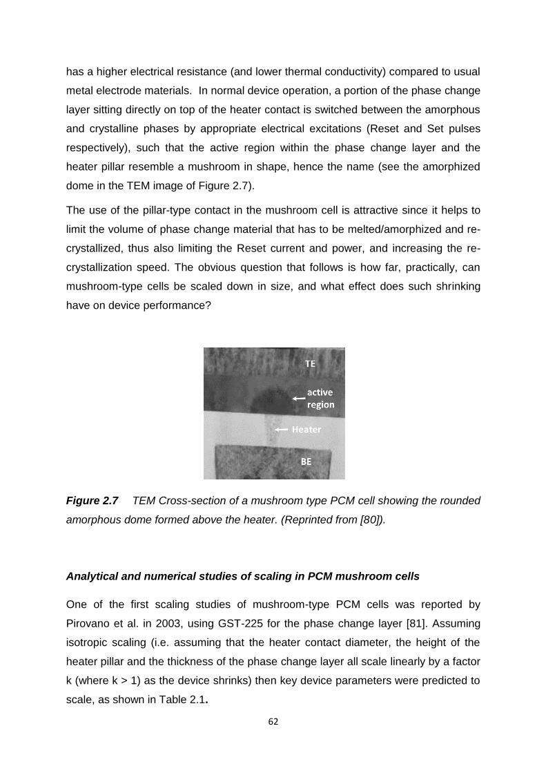
62
has a higher electrical resistance (and lower thermal conductivity) compared to usual
metal electrode materials. In normal device operation, a portion of the phase change
layer sitting directly on top of the heater contact is switched between the amorphous
and crystalline phases by appropriate electrical excitations (Reset and Set pulses
respectively), such that the active region within the phase change layer and the
heater pillar resemble a mushroom in shape, hence the name (see the amorphized
dome in the TEM image of Figure 2.7).
The use of the pillar-type contact in the mushroom cell is attractive since it helps to
limit the volume of phase change material that has to be melted/amorphized and re-
crystallized, thus also limiting the Reset current and power, and increasing the re-
crystallization speed. The obvious question that follows is how far, practically, can
mushroom-type cells be scaled down in size, and what effect does such shrinking
have on device performance?
Figure 2.7 TEM Cross-section of a mushroom type PCM cell showing the rounded
amorphous dome formed above the heater. (Reprinted from [80]).
Analytical and numerical studies of scaling in PCM mushroom cells
One of the first scaling studies of mushroom-type PCM cells was reported by
Pirovano et al. in 2003, using GST-225 for the phase change layer [81]. Assuming
isotropic scaling (i.e. assuming that the heater contact diameter, the height of the
heater pillar and the thickness of the phase change layer all scale linearly by a factor
k (where k > 1) as the device shrinks) then key device parameters were predicted to
scale, as shown in Table 2.1.
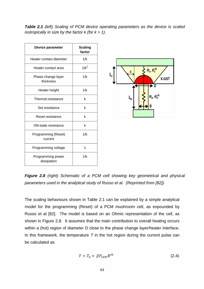
63
Table 2.1 (left) Scaling of PCM device operating parameters as the device is scaled
isotropically in size by the factor k (for k > 1).
Device parameter Scaling
factor
Heater contact diameter 1/k
Heater contact area 1/k2
Phase change layer
thickness
1/k
Heater height 1/k
Thermal resistance k
Set resistance k
Reset resistance k
ON-state resistance k
Programming (Reset)
current
1/k
Programming voltage 1
Programming power
dissipation
1/k
Figure 2.8 (right) Schematic of a PCM cell showing key geometrical and physical
parameters used in the analytical study of Russo et al. (Reprinted from [82]).
The scaling behaviours shown in Table 2.1 can be explained by a simple analytical
model for the programming (Reset) of a PCM mushroom cell, as expounded by
Russo et al [82]. The model is based on an Ohmic representation of the cell, as
shown in Figure 2.8. It assumes that the main contribution to overall heating occurs
within a (hot) region of diameter D close to the phase change layer/heater interface.
In this framework, the temperature T in the hot region during the current pulse can
be calculated as
(2.4)

64
where T0 is ambient (room) temperature, PGEN is the dissipated power within the
cell, Rth is the overall thermal resistance from the hot spot to the heat sinks (at T)
and is the fraction of total power dissipated in the hot region. PGEN in turn is given
approximately by
(2.5)
where RON is (electrical) resistance of the cell during programming. RON is given by
the serial combination of the heater resistance, Rh, and the phase change layer
resistance, Rc, i.e.
(2.6)
The thermal resistance, Rth, on the other hand, is given by the parallel combination
of the thermal resistance of the phase change layer, , and that of the heater,
(since heat can flow towards both top and bottom electrodes simultaneously), i.e.
(2.7)
The melting current Im then follows from eqn. (2.5), substituting for PGEN from eqn.
(2.4) with T = Tm and Rth from eqn. (2.7) to yield
(2.8)
To determine how Im (and thus the Reset current) scales with the scaling factor k, we
need in turn to determine how ,
and RON all scale with k. The heater thermal
resistance can be written (by analogy with electrical resistance R = L/A) simply as
(2.9)
where θh is the heater thermal conductivity, rh the heater radius and Lh its length. The
thermal resistance presented by the phase change layer can be found by calculating
the heat flow towards the top electrode (the top thermal contact). By assuming the
heat flows in a truncated cone of base diameter equal to that of the hot spot (D) and
having an angle of 450 (see Fig. 2.8), then can be calculated from
(2.10)
where θc is the thermal conductivity of the phase change layer and Lc its thickness.
Solution of the integral in eqn. (2.10) yields

65
(2.11)
Similarly, the electrical resistance of the heater is simply
(2.12)
where h is the heater’s electrical resistivity. The resistance of the phase change
layer can be given by analogy with eqn. (2.11), replacing D with the electrical contact
diameter (i.e. the diameter of the heater, ϕ), such that
ϕ (2.13)
Inspecting eqns. (2.9), (2.11), (2.12) and (2.13) we can see that as Lh, Lc and ϕ
(=2rh) are all scaled isotropically as 1/k (and note that D scales isotropically too),
then ,
and RON (where RON = Rc + Rh) will all scale as k. Thus, from eqn. (2.8) it
is easy to see that, under the conditions of isotropic scaling of the PCM cell by a
factor k, the melting current Im must scale as 1/k, as shown in Table 2.1.
Similarly, since the melting voltage Vm is given simply by
(2.14)
and the power by
(215)
we see that the melting voltage is constant with scaling (Im scales as 1/k, RON scales
as k), while the power dissipation for melting scales as 1/k (Im scales as 1/k, Vm
independent of k). The key role played by the scaling of the contact area (and
consequently the volume of phase change material that undergoes melting) in
reducing melting currents and powers (and hence Reset currents and powers) is
thus clearly evident, even from a simple analytical approach such as that presented
above.
Pirovano [81] and Russo [82] used analytical models such as those above, backed
up by numerical electrical and thermal simulations, to predict the variations of key
device operating parameters as device sizes shrink. Typical results, assuming a
GST phase change layer and a TiN heater, are shown in Figure 2.9 (taken from [82])
where the values of RON and Im are shown as a function of the technology node, F,
down to the 16 nm node (note that in Fig. 2.9 (a), ϕ is the actual heater contact

66
diameter (=2rh)). It is clear that shrinking of the device leads to improved
performance in key areas, in particular the reduction of the melting (Reset) current,
which drops from over 500µA at the 90nm node (heater diameter of 56 nm, or ~2500
nm2 heater contact area) to under 100 µA at the 16 nm node (heater diameter of
10nm, or ~80 nm2 heater contact area). The fact that the operating characteristics of
PCM devices improve as the devices become smaller is one of the most attractive
features of this technology – things get better as we make them smaller.
(a)
(b)
Figure 2.9 (a) Variation of PCM mushroom-type cell ON resistance as a function of
the technology node size (F); two cases are shown assuming isotropic and non-
isotropic scaling (see text). Numerical values for refer to the heater contact
diameter. (b) Variation in the melting (Reset) current as a function of the technology
node (F). (Reprinted from [82]).
Of course isotropic device scaling of the mushroom-type cell is not the only approach
to reducing critical operating parameters, such as the Reset current; there is also the
possibility of cell geometry optimization, the use of alternative cell designs, as well as
the use of alternative materials. Let’s consider first an approach based on possible
optimizations of the mushroom cell geometry. In the isotropic scaling discussed
previously, the phase change layer thickness (Lc), the heater length (Lh) and the
heater contact diameter ϕ were all scaled simultaneously by the same factor.
However, this need not be the case. One form of non-isotropic scaling is to keep Lc

67
and Lh constant while reducing the heater contact diameter (note that is the key
lithographically-limited dimension). Results for this case are also shown in Fig. 2.9,
where it can be seen that additional benefits, in terms of a stronger reduction in the
melting current with decreasing technology node, are possible. It should however be
noted that we cannot allow Lc and Lh to take on arbitrary values just so as to reduce
Im. This due to both manufacturing limitations and, importantly, the effect that Lc and
Lh have on the resistance of the PCM cell (see Figure 2.10), in particular the
resistance, RSET, when in the cell is in the crystalline state. This is because the value
of RSET affects the size of the readout current, the higher RSET the smaller the
readout current and the longer it takes to sense the state of the cell during readout
[38]. Since the values chosen for Lc and Lh will also alter the thermal (in addition to
electrical) resistances, as is evident from eqns. (2.6) to (2.9), they also affect very
considerably the temperature distribution in the cell, as shown in Figure 2.10 (b).
Note that the ‘optimum cell’ shown in Figure 2.10 (b) (and where the hot spot is
located close to the heater/phase change layer interface) is the structure chosen for
the isotropic scaling study the results of which are shown in Figure 2.9.
(a)
(b)
Figure 2.10 (a) The variation of melting current, Im, as a function of heater length, Lh,
for a fixed heater diameter of 30 nm and for a range of cell SET resistances, RSET
(the thickness, LC, of the phase change layer, GST in this case, was varied to
maintain a constant RSET as Lh varied). (b) Simulated temperature distributions in
mushroom-type PCM cells (each subject to their own individual melting current) with
different Lc and Lh sizes. (Both reprinted from [82]).

68
Experimental scaling of PCM mushroom-type cells
The first widespread reports on the performance of commercially-viable PCM
mushroom-type cells appeared for the (F=) 180 nm node in the late 1990s and early
2000s. Not surprisingly for such relatively large cells, key operating characteristics
such as the Reset current were relatively poor, for example a Reset current of
around 1 mA in [83]. However, even as early as 2003 experimental mushroom cells
with much improved performance were demonstrated, such as a 65 nm node cell
with 50 µA RESET current by Pirovano et al. [81]. Interestingly, Pirovano in the same
work also showed a factor of x2 reduction by moving from a mushroom cell design to
its effective ‘pore’ cell complement (discussed in section 2.2.3), showing that
switching current and power reductions could be achieved by judicious devices
engineering as well as via simple scaling.
Product-style PCM memories fabricated at the 90 nm mode were first revealed
around 2006, with, as expected, significantly improved performance as compared to
180 nm node devices. For example Pellizzer et al. [84] demonstrated arrays of
mushroom-type PCM cells having Reset currents of around 700 µA for a heater
contact area of approximately 3000 nm2 (i.e. a heater diameter of around 60 nm) and
a complete cell area (including the selector devices etc.) of 12F2. More recently IBM
have demonstrated 90 nm node mushroom-type PCM cells that can successfully be
used to store and recover up to 3 bits (or 8 separately differentiable resistance
levels) per cell (see Figure 2.11), significantly enhancing the potential storage
capacities of phase change memories [85]. Interestingly the same 90 nm node
mushroom-type cells have also been used to demonstrate some of the other
remarkable functionalities offered by phase change devices, including arithmetic
processing [86] and even the development of neuronal mimics for brain-like
processing [87].
Beyond (i.e. smaller than) the 90 nm node, the simple mushroom cell has not been
extensively utilized for product-oriented PCM memory development, rather variations
of it, such as the μTrench [88], dash-type [89, 90] and pore-cell have predominated
(see e.g. [91]). Such cell designs are discussed in the following sections.

69
(a)
(b)
Figure 2.11 (a) A 90 nm node mushroom-type PCM as developed by IBM to deliver
multi-level storage capability of up to 3-bits per cell. (b) Programming current versus
resistance curve for multi-level operation showing use of partial Reset to provide
multiple resistance levels. (Both reprinted from [85]).
2.2.2 The μTrench and Dash-type Cell
The μTrench structure reduces the switching volume in the phase change cell by
depositing the phase change layer into a lithographically-defined trench that
intersects with a thin, vertical heater electrode [88]. At the 90 nm node such cells
could be programmed (Reset) with a current of around 400 μA, compared to around
700 μA for a mushroom cell fabricated at the same technology node. A later variant
of the μTrench, the so-called ‘wall’ structure, was successfully used to develop a
1Gbit PCM array at the 45 nm node (with an effective cell size of 5.5F2) and a Reset
current of 200 μA [93].
The dash-type cell (shown in Figure 2.12), developed by Samsung, is fabricated by
first forming a sidewall electrode, recessing the electrode vertically and filling the
recessed volume with phase change material, then (after removal of any phase
change material from the top surface) depositing the top electrode. In this way the
active volume of phase change material can be dimensionally constrained to very
small volumes (since it is confined to the recessed volume), with a resulting
decrease in switching currents, as shown in Figure 2.12 (a) [89]. Indeed, dash-cells
with phase change volumes as small as 7.5 x 22 x 30 nm (width x depth x height)

70
were successfully fabricated at the 20 nm node and showed Reset currents below
100 µA, along with other excellent performance characteristics including around 1011
memory cycles without failure and projected lifetimes of more than 10 years at 85 0C
[90, 93]. Dash-type PCM arrays with a total capacity of 8 Gbits and a cell size of 4F2
at the 20 nm node were also demonstrated.
(a)
(b)
(c)
Figure 2.12 (a) Simulated Reset current amplitude as a function of the size of the
bottom electrical contact (BEC) for a mushroom-type cell (planar structure) and a
confined cell, showing expected reduction in Reset current for the latter. (Reprinted
from [89]). (b) Schematic of the dash-type version of the confined cell as developed
by Samsung. (c) TEM cross-sectional image of a dash-type cell. (Reprinted from
[93]).
2.2.3 The Pore Cell
The pore-type cell, as shown in Figure 2.13, is another approach that has been used
to confine the volume of phase change material that undergoes switching. By limiting
the phase change material that is in contact with the bottom heater electrode to a
small ‘pore’ region, the size of the hot-spot within the phase change layer is
effectively determined by the pore size (see Figure 2.13 (b)), with a consequent
reduction in active switching volume and a consequent reduction in switching current
and energy (shown in Figure 2.13 (c)).

71
(a)
(b)
(c)
Figure 2.13 (a) TEM cross-sectional image of a GST pore-type cell. (b) Simulation of
temperature distribution in GST layer during Reset process, showing successful
confinement of the heated volume. (c) Simulated effect of pore diameter and slope of
SiN sidewall on Reset current. (All reprinted from [50)).
So far in this chapter the main concern has been the effect of device scaling on
switching current requirements, specifically the Reset (or melting) current, since it is
this that determines the energy/power consumption of the device and the current-
driving requirements of the individual cell-selector electronics (and whose size also
depends on the current they are required to supply). However, it is also important to
consider other switching characteristics and how these are affected by the scaling of
the cell size. In particular, the switching speed is an important criterion that should
not be overlooked. Since amorphization processes are de facto fast – once we have
heated the active region up to the melting temperature it has to be cooled down at
very fast rates, typically > 40 Kns-1, in order to freeze into the amorphous phase
(rather than re-crystallize) – it is the crystallization process that dominates the overall
speed of operation of PCM devices. The rate of crystallization is determined by the
crystal nucleation rate and the crystal growth rate (both of which are of course
functions of temperature), and clearly the smaller the volume of amorphized material
that is required to be re-crystallized in a cell, the quicker that re-crystallization
process will be (assuming that said volume contains or can generate sufficient
crystal nuclei during the crystallization process and/or borders a region that is
already crystallized and can grow into the amorphous volume).

72
The interplay between active phase change volume and switching speeds has thus
been studied by several researchers using pore-type cells. For example Wang et al.
[94] fabricated GST pore-type cells with bottom contact sizes (diameters) ranging
from 500 nm down to 19 nm and investigated the switching speed as a function of
cell size. Extremely fast, for PCM, switching was obtained for the smallest cells, with
2.5 ns Set and 400 ps Reset pulses (of 0.8 V and 4.5 V respectively) being reported.
(a)
(b)
Figure 2.14 (a) Set voltage versus pulse width for pore-type cells of 50 nm in
diameter with and without the aid of a 0.3 V “incubation-field”. Without the
incubation-field the shortest Set pulse that switched the cell to the low resistance
state was 10 ns, whereas with incubation it was 500 ps. (b) Shows successful
repeated switching of the cell in (a) with 500 ps pulses for both Set and Reset. (Both
from [95]).
Subsequently, by exploitation of an incubation pulse prior to the main switching pulse
(essentially a form of pre-heating of the cell so as to control nucleation) and again
using pore-type cells, Loke et al. [95] were able for the first time to demonstrate
successfully the PCM cell crystallization using sub-ns, specifically 500 ps, Set pulses
(see Figure 2.14). Such an improvement in switching speed with device scaling
provides a very welcome added benefit and opens up the possibility of using PCM
devices in areas not previously thought practicable, such as in DRAM replacement.

73
2.2.4 Crossbar Cells
Crossbar cells (shown in Figure 2.15) have gained significant interest in recent years
as they provide the possibility for 3D memory layer stacking and high scalability [96,
97, 98]. In a crossbar cell, the active material is placed at the intersections of cross-
wise (orthogonal) patterns of metal lines, the so-called bit line (BL) and word line
(WL), and SET/RESET excitations placed on a bit-line/word-line pair are passed to
the phase change cell via an integrated selector device (ideally a diode to limit area
footprint), see Figure 2.15 (a). The active volume of phase change material is
essentially determined by the size of the electrodes, with an approximately ten-fold
reduction in Reset current (from > 1500 µA to 160 µA) having been reported [97] as
contact sizes were reduced from 150 nm to 30 nm (see Figure 2.15 (c)). A stackable
and scalable crossbar cell using a chalcogenide threshold-switch (also known as
Ovonic Threshold Switch, or OTS) as the selector, rather than an integrated Si-diode
has also been demonstrated, opening up the exciting prospect of an entirely
chalcogenide-based crossbar type memory [96].
(a)
(b)
(c)
Figure 2.15 (a) Schematic of a crossbar type PCM structure with integrated Si-diode
selector. (Reprinted from [97]. (b) TEM cross-sectional image of a crossbar device.
(Reprinted from [98]). (c) Reset current scaling characteristics of a PCM crossbar
device showing a ten-fold reduction in current as the contact size shrinks from 150
nm to 30 nm. (Reprinted from [97].

74
2.2.5 Probe-based Phase Change Memory Cells
Another viable approach to scale the volume of the active phase change material,
and consequently achieve ultrahigh storage densities (Terabit per square inch, or
simply Tb/in2), is by the application of scanning probe microscopy technology, which
is commonly referred to as ‘phase change probe storage’. The concept of using
scanning probe-based techniques for storage devices was first demonstrated by IBM
in 2002 in their ‘Millipede’ system, where a 2-dimensional array of one thousand
thermo-mechanical probes was used to write, read and erase indentations in a
polymer medium, achieving storage densities of up to 1 Tb/in2 [99] (see Figure 2.16
(a)). Particularly, in phase change probe storage, Hamann et al [100] demonstrated
the scalability of thermal recording of erasable bit-patterns in 18nm thick GST films
at ultrahigh storage densities of up to 3.3 Tb/in2, which remains the largest storage
density achieved to date using phase change materials (see Figure 2.16 (b)).
However, the mechanism employed by Hamann et al to achieve this storage density
was thermal, as opposed to electrical storage, which is generally considered to be
more advantageous due to the following reasons.
The writing process of electrical probe storage induces lower power
consumption in comparison to other technologies (0.1nJ per written bit
compared to the IBM Millipede’s 10nJ per written bit) [78]
The use of electrical probe storage results in a higher spatial resolution in
comparison to magnetic and thermal technologies due to a self-focusing effect
of the current lines linked to the non-linear thermal and electrical responses of
the storage medium
The tip shape can be smoother in comparison to other technologies, which
require very sharp tips, since in electrical probe storage the main requirement
is the passing of current through the contact area between the tip and the
sample

75
(a) (b)
Figure 2.16 (a) The IBM ‘Millipede’ concept consisting of a 2-D array of probes
used to write, read and erase indentations in polymer media (Reprinted from [99]).
(b) Experimental setup by Hamann et al for phase change thermal recording (top),
and crystalline bits written in an amorphous GST film using a heated AFM tip
(bottom), achieving storage densities of up to 3.3. Tb/in2 (Reprinted from [100]).
(a) (b)
Figure 2.17 (a) Schematic of the write (top) and read (bottom) processes in phase
change probe storage (Reprinted from [101]). (b) Phase change probe memory cell
structure used by Wright et al to demonstrate 1.5 Tb/in2 storage densities (Reprinted
from [78]).

76
Electrical Probe Storage in GST films
A typical electrical phase change probe memory cell comprises a phase change
material layer sandwiched between two electrodes i.e. a bottom metal electrode and
a top electrode typically comprising a conductive atomic force microscopy (C-AFM)
tip (Pt, Si, PtSi, Au etc) and a conductive capping layer which prevents the phase
change material from oxidation, while at the same time providing good tribological
properties to allow the tip to move smoothly over the surface and protecting it against
scan wear (of both the tip and the medium). The sharp C-AFM tip, attached to a
cantilever, is brought close to or in contact with the sample surface, and a voltage is
applied between the conducting tip and the sample (deposited on a Si substrate) to
form amorphous and crystalline bits, thus providing a phase change memory device
with, ultimately, atomic resolution. The basic mechanism for phase change probe
storage is shown in Figure 2.17 (a) [101].
Gidon et al [102] used a multilayer structure comprising a 30nm thick GST layer,
2nm and 10nm thick diamond-like carbon (DLC) capping and underlayers
respectively, deposited on a Si substrate. It was shown that crystalline dots as small
as 15nm could be written (using a 6V pulse) and read (using a 1.7V pulse)
repeatedly, demonstrating that Tb/in2 storage densities could be achieved in phase
change media. A similar structure (DLC (2nm) / GST (30nm) / DLC (10nm) / Si) was
also used by Wright et al [78] (shown in Figure 2.17 (b)) to demonstrate theoretically
the possibility of Tb/in2 storage densities in probe-based PCM. 10-30nm sized
amorphous and crystalline bits were written and read in the GST layer using a Si C-
AFM tip (10nm radius) with low Reset and Set energies (300pJ and 100pJ
respectively) predicting storage densities of up to 1.5 Tb/in2 [78]. Wright et al further
demonstrated rewritability in probe-based PCMs in [103] by using a more optimized
cell structure by replacing the Si tip and DLC underlayer with an encapsulated PtSi
tip and TiN bottom electrode respectively. Firstly, amorphous bits were written into a
crystalline GST layer and then erased by re-crystallization, and secondly, crystalline
bits were written into an amorphous GST layer and subsequently erased by re-
amorphization. It was demonstrated that in conventional phase change materials,
such as GST films, this approach invariably leads to the formation of a crystalline
‘halo’ (ring) surrounding the erased (re-amorphized) region, which can have severe
consequences on the achievable density in real devices. To overcome this, the use

77
of patterned media (discussed later in this section) or slow-growth phase change
media was proposed [103].
Although carbon capping layers have been frequently used in probe-based PCM
cells (for example [78, 102, 103]), Tanaka et al [104] reported an alternative method
to experimentally write, read and erase 10-100nm sized amorphous and crystalline
bits in 500nm thick GST films by immersing the entire storage medium in an inert
liquid (3M Fluorinert FC-43, see [105]), and using a homemade Gold C-AFM tip to
make direct contact with the GST layer. This immersion of the storage medium in an
inert liquid meant no capping layer was required to prevent the GST layer from
oxidation. This was the first time amorphous bits were experimentally written in a
crystalline GST material using C-AFM probes [104].
Patterned Probe Phase Change Memory (PP-PCM) Cells
An alternative approach for the scaling of probe-based PCM cells and subsequently
enhancing their storage densities is by the use of ‘patterned media’. A typical PP-
PCM cell consists of small (nanoscale) phase change regions isolated from each
other by a thermal insulator (e.g. SiO2) to form storage bits (see Figure 2.18), as
opposed to phase change films discussed previously.
(a) (b)
Figure 2.18 (a) Schematic diagram of patterned probe PCM (PP-PCM) cells
proposed by Kim et al [106] to demonstrate electrical switching on the micrometer
scale. (b) SEM image of the 2D-arrayed PP-PCM cells (Reprinted from [106]).
Pint

78
Kim et al [106] demonstrated that patterned PCM cells are an alternative approach to
achieve reversible phase transitions using C-AFM probes. In their study, a 2D-array
of GST cells with a size of 20x20 μm2 separated by SiO2 insulations were fabricated
using photoresist patterning, followed by the deposition of 100nm thick TiN top
electrodes onto each GST cell using dc-magnetron sputtering. 10V/50ns (Reset)
and 5V/300ns (Set) pulses were applied using a large (18 μm) Tungsten C-AFM tip
to reversibly switch the GST layer from crystalline to amorphous, and amorphous to
crystalline states, respectively. A two orders of magnitude resistance difference
between the two phases was reported, showing the viability of PP-PCM cells.
However, one of the drawbacks of Kim’s study was that the cell dimensions were on
the micrometer scale, which is undesirable for real devices. To address this
limitation, Yoon et al [107] fabricated much smaller (30nm) conical-shaped
TiN/GST/TiN PP-PCM cells, and demonstrated reversible switching using Reset and
Set pulses of 1.8V/100ns and 1.2V/100ns respectively. A threshold switching
voltage of 1.1V and a Reset current of 100 μA was reported. Moreover, Yoon et al
showed that using this cell array, storage densities of 207 Gb/in2 could be achieved
in PP-PCM cells.
Table 2.2 compares the storage density performance of PCM with other probe-based
memory technologies [108].
Table 2.2 Storage density comparison of various probe-based memory
technologies (Adapted from [108]).
Magnetic
probe storage
Thermomechanical
probe storage
Ferroelectric
probe storage
Phase Change
probe storage
Storage Density
60 Gb/in2
4.0 Tb/in2
4.0 Tb/in2
- 3.3 Tb/in2 using
thermal storage
- 1.5 Tb/in2 using
electrical probe storage

79
2.2.6 Carbon Nanotube-based Cells
To reduce the contact area to the sub-10 nm2 region, and so probe the ‘ultimate’
scaling capabilities of phase change memories, several authors have reported the
use of carbon nanotube (CNT) electrodes having diameters typically in the range 1
to 6 nm [109, 110, 111]. For example, in seminal work by Xiong et al. [109], working
phase change memories were fabricated by forming (via electrical breakdown) a
nanogap along the length of a carbon nanotube, then filling the nanogap with a thin
phase change layer (10 nm of GST in this case), see Figure 2.19. Although the
phase change layer was not laterally confined, i.e. it extended laterally far beyond
the diameter of the CNT itself, the written bits themselves appeared to be well
confined (due to thermal effects) to lateral sizes similar to the CNT diameter (see
Figure 2.19 (a)), meaning that the effective bit volumes were as small as a few
hundred cubic nanometres.
(a)
(b)
Figure 2.19 (a) AFM images of a CNT-based nanogap PCM cell before (left) and
after (right) filling with GST (the scale bars are 500 nm). (Reprinted from [109]). (b)
Ultra-low programming currents achieved for several CNT-based nanogap PCM
devices having ultra-small contact diameters (blue and red dots correspond to
devices where the formation of the nanogap was carried out in air and Ar
respectively). (Adapted from [109]).
By using nanotubes of various diameters Xiong et al. were able to determine the
scaling properties of their CNT-based PCM devices, finding Reset currents as low as
5 µA (and Set currents below 1 µA) for the smallest devices having a contact

80
diameter of around 2 to 3 nm. In subsequent work, Xiong et al. [111] developed a
fabrication technique (involving a form of phase change nanowire being deposited
into a nanotrench formed around the CNT) to limit the dimensions of the phase
change layer in the lateral direction perpendicular to the CNT nanogap. This reduced
the effective contact area still further (to ~ 2.5 nm2, diameter ~ 1.8 nm) as well as any
lateral spread of heat (as compared to [109]), resulting in Reset currents as low as
1.6 µA being achieved. Liang et al. [110] were also able to obtain ultra-low
programming currents in CNT-based cells having contact areas of ~ 2.5 nm2, but
using a crossbar-type device configuration (discussed in section 2.2.4) more closely
related to product-like device architectures.
Along with the dramatic reductions in programming currents achieved using CNT-
based PCM cells, also come vast reductions in programming power and energy. For
example, the nanogap devices reported by Xiong et al. [109] achieved Reset powers
of a few µW (cf. ~ mW programming power for product-like devices) and Reset
energies of around 100 fJ for 20 ns Reset pulse lengths. Further reductions in
switching energies would be expected for smaller bits and faster pulses. Indeed,
Xiong et al. speculated that if the nanogaps were to be reduced in length to around 5
nm, then the active switching volume in their CNT-based cells would be reduced to
around 20 nm3 and the resulting Set and Reset energies would fall as low as 5x10-18
and 2x10-17 J respectively (i.e. 5 aJ and 20 aJ) - truly miniscule values. And, even if
such small switching volumes (~ 20 nm3) were to be achieved in some ‘ultimately-
scaled’ device, these would still be substantially larger than the 2 nm diameter (~4
nm3) nanoparticles that have been shown experimentally to successfully crystallize
(see e.g. Figure 2.5 (b)), would still be substantially larger than the theoretical
minimum crystallite size predicted by classical nucleation theory (e.g. ~ 0.5 to 1 nm3
for GST, see Figure 2.6 (a)) and by atomistic simulations (e.g. 1.5 to 3 nm3 for GST,
see Figure 2.6 (b)), meaning that even smaller working cells might be imagined.
2.3 The Role of Thermal Engineering in Scaling
In the previous sections, the effects of PCM cell size and cell design on the device
operating characteristics as a function of scaling have been considered. A key
benefit of scaling has been seen to be the reduction of Reset current (and hence

81
device operating power/energy) as cell sizes shrink. However, since the phase-
transformation process in PCM cells is essentially thermally-driven, by judicious
thermal engineering of the cell we might also expect to realise benefits in terms of a
reduction in programming current. Essentially we would like to thermally-engineer
the cell so as to retain, in the active switching volume, as much heat as possible (so
maximising the temperature rise per unit excitation current), while at the same time
ensuring that the melted phase can cool fast enough (i.e. greater than several tens
of Kelvin per nanosecond) for re-solidification to occur into the amorphous phase.
These two thermal requirements are in essence in opposition to each other, but
nonetheless, by careful design we can indeed fulfil both requirements and yield
certain device performance improvements.
Graphene has recently been found to be a promising candidate for providing effective
nanoscale electrical contact in PCM cells. This is mainly due to its atomically thin
nature, chemical inertness (strong sp2 bonds) and high electrical conductivity. In
addition, lower current consumptions, and enhanced endurance levels have also
been reported using graphene as an electrical contact in PCM cells [112, 113]. For
example, Ahn et al [112] inserted a graphene layer at the interface between GST and
a bottom electrode (Tungsten) heater resulting in a ~40% lower Reset current
compared to notionally identical control devices without the graphene layer. The
authors attributed this mainly to the added interfacial thermal resistance which
resulted in heat confinement inside the GST layer. An endurance of up to 105 cycles
was also achieved using Graphene-PCM (G-PCM). Although initial findings using
Graphene within PCM are encouraging, further research is required to determine the
commercial viability of G-PCM devices.
Since most heat is lost from a PCM cell via the usually high thermal conductivity
electrodes, another more viable approach to thermally-engineer a reduction in
programming current is to modify in some way the commonly used electrodes (such
as TiN and W) to reduce their thermal conductivity, while at the same time
maintaining adequate electrical contact. For example, Lu et al. [114] found that by
stacking many thin layers of TiN and W together to create a superlattice-like top
electrode structure (see Figure 2.20 (a)), the thermal conductivity (which is typically
greater than 10 and 100 W/mK for single layers of TiN and W)can be reduced to
below 1 W/mK while retaining good electrical conductivity. The authors varied the

82
(a) (b)
Figure 2.20 (a) Stacked TiN/W electrode structure used by Lu et al to enhance
thermal confinement in 190nm sized PCM cells. (b) Thermal conductivities and
resistivities of 3-7, 5-5, 7-3 (nm) TiN-W electrode layers. Much lower thermal
conductivities were observed for stacked electrodes in comparison to single layer
TiN and W electrodes. (Reprinted from [114]).
ratio of TiN-W from 3-7, 5-5, 7-3 (nm in thickness) and reported thermal conductivity
values of 0.43, 0.42 and 0.44 W/mK respectively, which was much lower than single
TiN and W layers (see Figure 2.20 (b)). However, the work of Lu et al was confined
to very large PCM cell sizes (190nm diameter heater contacts).
2.4 Chapter Summary
It is clear from the discussions in this chapter that we have come a long way towards
answering many of the key questions in terms of how far phase change materials
and memory devices can be scaled down in size and still function adequately. The
discussions in Section 2.1 show that phase change materials can typically be scaled
down in one—dimension, two-dimensions, and three-dimensions. It has been shown
that phase change materials do indeed have the capability to switch between phases
at single-nanometer dimensions, and the crystallization temperature, Tx, typically
increases at these dimensions. On the other hand, depending on the phase change
material being used, the crystallization speed (especially for nucleation-dominated
materials (such as GST)), and the thermal conductivity, k, can decrease when
materials are scaled down to smaller dimensions. It has also been shown that the

83
ultimate scaling limit after which phase change materials do not crystallize anymore
(i.e. from an amorphous starting phase) is 1-2nm. This is set by the fact that at least
a few atoms are needed to transform the material to a crystalline phase, which is
reached in this range. Section 2.2 further presents a detailed review of the
scalability of various traditional and emerging PCM cell structures. Indeed as PCM
cells become smaller they function more adequately, in fact they function
significantly better than larger cells in terms of device operating parameters, in
particular programming currents are reduced, switching speeds increase, and
storage densities increase. The scaling down of PCM cell size is notably beneficial
with regards to the reduction of the Reset current, which is probably the critical
device characteristic in terms of the commercial viability of this technology. Various
traditional and more viable cell structures (such as mushroom-type, μtrench, dash,
crossbar, pore and probe-based PCM cells) have been used widely in PCM, with the
mushroom cell being the most widely used conventional PCM cell structure. In
addition, various emerging but less commercially viable cell structures (such as
carbon nanotube-based and graphene-based cells) have also been proposed in the
literature to overcome some of the challenges associated with traditional PCM cell
structures. In particular, Reset currents in the range of 1.5 - 5 μA have been
achieved using carbon nanotube electrodes with GST as the active material
(although, to re-iterate, such ‘exotic’ cell structures are not commercially viable for
real PCM devices).
It is clearly evident that PCM, and particularly the scalability of PCM, has come a
long way from when research on this technology first started in the 1960s. However,
some key questions related to the scalability of PCM still remain unanswered (see
section 1.5). This thesis aims to answer these questions in Chapters 4, 5, 6, 7 and 8
by using a physically realistic and sophisticated Multiphysics Cellular Automata
approach, which combines electro-thermal simulations with the Gillespie Cellular
Automata (GCA) phase change model. Details of the characteristics and
implementation of this PCM device modelling approach have been presented in the
following Chapter 3.

84
Chapter 3 Simulation of Phase Change Devices using a Multiphysics Cellular Automata Approach
Phase change materials have, as described in Chapters 1 and 2, been used extensively
for optical storage applications and, in recent years, for electrical phase change memory
(PCM) applications. Furthermore, PCM devices have shown great potential to scale
down to extremely small dimensions with improved performance characteristics, such
as lower current consumptions, faster switching speeds and enhanced storage
densities. It is important to notice that the physics of the phase transition for electrical
PCM is different to that of optical storage i.e. optical storage is dependent on a pure
thermal process, whereas electrical PCM involves both electrical and thermal (electro-
thermal) processes. Hence, it is crucial to develop physically realistic models for the
electrical, thermal and phase change processes to understand the fundamental physics,
and in order to achieve better design and optimization of PCM devices.
A fully coupled electro-thermal/phase change model for the simulation of phase change
memory materials and devices typically consists of three sub-models; an electrical
model, a thermal model, and a phase change model (see Figure 3.1). The following
sections 3.1 and 3.2 describe the details of the electrical and thermal models used for
the work in this thesis. Following these descriptions, section 3.3 presents a review of
the various phase change models typically used to simulate the phase transitions in
phase change materials and devices. Furthermore, a comparison of these phase
change models, and the characteristics and advantages of using the Gillespie Cellular
Automata (GCA) model (used for the work in this thesis) over other models, such as the
JMAK, Classical Nucleation and Growth, Rate Equation-based methods and Atomistic
modelling is also presented. The chapter is then concluded in section 3.4 with a
description of the implementation of the fully coupled Multiphysics Cellular Automata
model used for the simulations of phase change devices in the following chapters of this
thesis.

85
Figure 3.1 Block diagram of a physical model for the simulations of electrical PCM
devices. J, K, and are the current density, thermal conductivity, and electrical
conductivity in the phase change material, respectively.
3.1 Electrical Model
For electrical switching (Reset and Set processes) in PCM devices, current is injected
into the phase change material through a conductive electrode resulting in Joule heating
which causes the material to switch between the amorphous and crystalline states. The
main purpose of developing an electrical model is to provide a current density
distribution inside the phase change material. This current density distribution is
modelled by solving the well known Laplace equation:
(3.1)
where V is the electrical potential, is the electrical conductivity and is the gradient
operator.
As shown in equation (3.1), the only parameter required is the electrical conductivity,
which needs to represent the electrical characteristics of the phase change material.
Wright et al [78] proposed an electrical model using the Laplace equation to study the
phase transformations in GST-based memory cells. Section 1.2.2 discussed that
reversible transitions between the highly resistive amorphous state and conductive
Phase change model
Electrical model
Thermal model
Change J, ơ
Joule heating

86
crystalline state can be observed in amorphous phase change materials. Their model
took this threshold switching behaviour into account by introducing temperature and
electric field dependencies of the electrical conductivity, , of the amorphous phase
change material using the following equation [115, 116]:
.
(3.2)
where is the electrical conductivity of GST in the amorphous phase, is a
constant, ∆
is the activation energy for the temperature dependence of . The
values of and ∆
are obtained by fitting to experimental data or from reported
literature [117, 118]. E is the electric field and E0 is the critical electric field at which
threshold switching takes place (with E0 typically 5 x 10⁷ V/m [119]).
In this model, the electrical conductivity of the crystalline phase change material
behaves in a way which conforms to an Arrhenius relation [118] as follows:
.
(3.3)
where σcryst is the electrical conductivity of GST in the crystalline phase, 0cryst is a
constant, and ∆ is the activation energy for the temperature dependence of cryst in
the crystalline state. Similar to and ∆ for the amorphous conductivity, 0cryst and
∆ are also obtained by fitting to experimental data [118].
The electrical conductivity of a phase change material, such as GST, depends on the
fraction of the crystallized material. The theory of percolation [120] is widely used to
describe the variation of electrical conductivity in a phase change material. Percolation
typically leads to a sharp switch from insulation to conduction when a fraction of a
conductive medium in an insulating matrix exceeds 15%. Therefore, a reasonable
approach for the electrical conductivity of GST is to switch the conductivity from that of
the amorphous state to that of the crystalline state when the crystalline fraction exceeds
a value of 15% [117]. Hence, the electrical model described in equations (3.1), (3.2)
and (3.3) is coupled with the mentioned percolation condition to simulate the electrical
switching of the phase change devices (i.e. if the fraction of crystallized material in a

87
simulation cell exceeds 15%, the electrical properties of that cell are assumed to be
those of the crystalline phase; if the fraction is less than 15%, the electrical properties of
the cell are assumed to be those of the amorphous phase)
.
3.2 Thermal Model
In the switching process of a phase change material, an electric current generates a
heat source, calculated using the electric model discussed in section 3.1. As a result, a
heat diffusion process creates a temperature distribution through the material, which is
obtained by solving the following heat transfer equation:
(3.4)
where ρ is the density of the material, Cp is the specific heat capacity per unit mass, k is
the thermal conductivity of the material, and Q is the heat source generated per unit
volume inside the material expressed by Q = E.J, where E and J are the electric field
and the current density inside the material respectively.
The thermal properties of a phase change material, GST in this case, exhibit a
thermally-dependent characteristic, and the thermal conductivity plays a dominant role
in determining the heat conduction inside the GST material. At room temperature, the
thermal conductivity of GST in amorphous state was reported to be 0.19 W/m.K, and in
crystalline state it was reported to be 0.5-0.58 W/mK [121-124]. The specific heat
capacity for GST was reported by Kuwahara et al [125] to be 210 J/kg.K at room
temperature, and it was shown to increase from 220 J/kg.K to 260 J/kg.K when the
temperature increased from 100oC to 500oC. For the case of the density, it was
reported by Wang et al [126] to be 5870 kg/m3 for amorphous GST, and 6270 kg/m3 for
crystalline GST. In addition, similar to the case of electrical conductivity in section 3.1,
the thermal conductivity of GST is also assumed to switch from amorphous to crystalline
values when the percolation value of 15% is reached, as shown by Wright et al in [117].
The reported thermal parameters discussed in this section have all been used in the
thermal model in this thesis to match realistic conditions.

88
3.3 A Review of Phase Change Models
A phase change model is required to simulate the crystallization (Set) and
amorphization (Reset) processes in phase change materials. As discussed in Chapter
1, an electrical pulse is applied to induce resistive heating (Joule heating) in the phase
change material: heating the material above melting temperature followed by a fast
quenching process freezes the material into the amorphous phase, and heating it to a
temperature below the melting temperature crystallizes the amorphous material. To
model the crystallization and amorphization behaviour of phase change memory
materials and devices, a number of phase transition approaches such as the (1)
Classical nucleation-growth theory, (2) Johnson-Mehl-Avrami-Kolmogrov (JMAK)
model, (3) Rate Equation-based methods, (4) Atomistic (ab-initio) modelling, and the (5)
Gillespie Cellular Automata (GCA) model have been presented. Sections 3.3.1 - 3.3.6
review and compare the characteristics of these phase change models, and show that a
sophisticated model such as the GCA approach presents significant advantages over
other simplistic approaches in use today for phase change device modelling.
3.3.1 Classical nucleation-growth theory
The classical theory of steady state crystal nucleation was developed by Gibbs, Volmer,
Weber, Becker, Doring, Turnbull and Fisher in 1926-1969 [29]. The main driving force
for crystallization in this approach is the difference in the Gibbs free energy of the
amorphous and crystalline phases of the phase change material. The classical
nucleation-growth theory proposes that the crystallization of an amorphous material
starts with the forming of small, unstable clusters [127, 128] which become stable once
the clusters reach a critical size (they become nuclei which can grow rather than being
dissolved). This approach further proposes that nucleation can occur in two different
ways: (1) homogeneous nucleation, in which nucleation can take place in any region of
the amorphous material, and (2) heterogeneous nucleation, in which nucleation can
occur at surfaces, interfaces and impurities [77].

89
The steady-state homogeneous nucleation rate Ihom is expressed as [128]:
(3.1)
, (3.2)
where hom is a pre-factor, Ean is the activation energy for nucleation, ∆Gc is the excess
free energy for the formation of a stable nuclei, * is the interfacial energy and ∆g is the
Gibbs free energy difference between the crystal and the supercooled liquid.
The steady state heterogeneous nucleation rate Ihet is expressed as [129]:
(3.3)
where het is a pre-factor, f(θ) is a shape factor, with other parameters as described in
(3.1). f(θ) is expressed as follows [128]:
θ θ θ
, (3.4)
where θ is the wetting angle of the nucleus at the surface of a substrate material.
Once nuclei are formed, crystalline clusters are assumed to change sizes by the
attachment and detachment of so-called ‘monomers’ (i.e. the basic building block of the
crystal phase). The expression for the growth rate was proposed by Meinders [130] as
follows:
(3.5)
where V0 is a pre-factor for the growth-velocity, Eag is the activation energy for growth,
and other terms as described in (3.1) and (3.2).
The classic nucleation theory enables the estimation of the cluster nucleation and
growth rate along with the crystallite size distribution. The assumptions for this theory
can be summarized as follows:

90
The formation and loss of new and old clusters is balanced, which is true at the
onset stage of crystallization. However, the nucleation rate decreases at a later
stage due to the continuous depletion of the amorphous phase change material.
Nuclei larger than the critical size are assumed to grow rather than shrink in size.
Although this assumption might be true for nuclei significantly larger in size
compared to the critical size, a dissolution process must also be involved for nuclei
with sizes near to the critical size.
In addition to the limitations mentioned above, simulations of phase change memory
devices requires the handling of nucleation and growth in very short time scales, where
transient and non-equilibrium conditions determine the crystallization process [77]. As a
result, an approach that can handle both nucleation and growth effects simultaneously
by taking transient effects into account is more desirable.
3.3.2 Johnson-Mehl-Avrami-Kolmogorov (JMAK) model
The JMAK model allows approximate calculations of the volume fraction of crystallized
material, whereas the classical nucleation-growth theory enables us to estimate the
cluster nucleation and growth rates, and crystal size distributions [131, 132, 133]. The
fraction of the crystallized material, X is given in the JMAK model as:
(3.6)
where X(t) is the volume fraction of the crystallized material at time t, n is the Avrami
coefficient, and k is the crystallisation rate constant given by the following Arrhenius
equation:
(3.7)
where v is a frequency factor, Ea is the activation energy, T is the absolute temperature,
and kB is the Boltzmann constant.
It is important to note that the JMAK approach is based on some assumptions [77],
which are often violated in real systems. These assumptions are as follows:
91
Nucleation takes place randomly and uniformly.
The nucleation rate is independent of time.
The growth rate is independent of cluster size.
Growth is dominated by interface control.
Some of the above assumptions are not always fulfilled in real systems. Firstly,
nucleation can occur at surfaces, interfaces, and impurities, well known as
heterogeneous nucleation [134, 135]. Experimental evidence has shown that the
interface layer between a substrate and a phase change layer is often where
crystallization starts, and the influence of heterogeneous nucleation at the substrate has
been studied by Ohshima in [134]. Secondly, an incubation time exists before the onset
of the crystallization process, which determines that the nucleation rate can not be
considered to be time independent over the entire crystallization process [136].
Experimental evidence has also shown the existence of non-negligible incubation time
during the crystallization of GST [136, 137]. Hence, the use of the JMAK approach is
not particularly appropriate for the simulation of the phase transformation in phase
change materials and memory devices [138].
3.3.3 Rate Equation-based methods
During the nucleation process in a real system, there is not only a distribution of clusters
of critical size, but also a distribution of different sized clusters. It is the interaction
between these clusters that determines the progress of the crystallization process [77].
Assuming that the smallest possible existing cluster size consists of two monomers, and
the growth and decay of clusters takes place by the attachment and detachment of
single monomers respectively, a continuous kinetic rate equation describing the
concentration f (n, t), of the clusters of size n is given by:
(3.8)

92
where g(n, t) and f(n, t) are the growth and dissolution rate respectively of a cluster of
size n. For the solution of the rate equation (3.8), the growth and dissolution rates need
to be determined, which can be obtained using the reaction rate theory [128]:
(3.9)
(3.10)
where f(1, t) is the concentration of monomers at a given time, r is the cluster radius, γ
is the molecular jump frequency at the interface between the amorphous and crystalline
states, and λ is the jump distance. The energy terms in the Boltzmann factors are
defined as the free energy differences between sizes n and n+1 such that:
(3.11)
where ∆G is the free energy required to form the new phase. By solving the set of
equations given by equ. (3.8), the size distribution of crystalline clusters at any given
time during the phase change process can be obtained.
Senkader and Wright [77] proposed a rate equation-based model to simulate the
crystallization behaviour in GST. In this model, the fraction of the crystallized material is
computed by the integration of the size distribution function in order to make a direct
comparison with experimental results. The heterogeneous nucleation (not considered
in the JMAK model) was taken into account by the introduction of a ‘spherical-cap’
model [139]. In this model, the nucleation of crystalline clusters takes place
preferentially at the GST/substrate interface and the shape of the crystal nuclei is
determined by the radius and wetting angle θ. The crystalline fraction predicted by the
proposed rate equation model was further validated with experimental results, as shown
in Figure 3.2 [77]
In comparison to the JMAK and Classical Nucleation and Growth approaches, the rate
equation-based methods provide a more physically-realistic approach for simulating and
studying the nucleation and growth processes simultaneously in phase change
materials. However, this approach introduces a large number of complex coupled
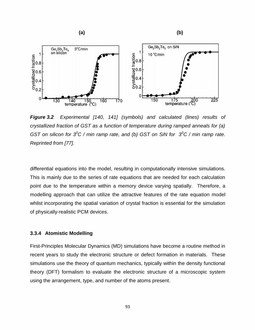
93
(a) (b)
Figure 3.2 Experimental [140, 141] (symbols) and calculated (lines) results of
crystallized fraction of GST as a function of temperature during ramped anneals for (a)
GST on silicon for 30C / min ramp rate, and (b) GST on SiN for 30C / min ramp rate.
Reprinted from [77].
differential equations into the model, resulting in computationally intensive simulations.
This is mainly due to the series of rate equations that are needed for each calculation
point due to the temperature within a memory device varying spatially. Therefore, a
modelling approach that can utilize the attractive features of the rate equation model
whilst incorporating the spatial variation of crystal fraction is essential for the simulation
of physically-realistic PCM devices.
3.3.4 Atomistic Modelling
First-Principles Molecular Dynamics (MD) simulations have become a routine method in
recent years to study the electronic structure or defect formation in materials. These
simulations use the theory of quantum mechanics, typically within the density functional
theory (DFT) formalism to evaluate the electronic structure of a microscopic system
using the arrangement, type, and number of the atoms present.

94
To model the crystallization process in phase change materials and memory devices,
various models have been developed based on DFT [29, 30, 142]. MD simulations are
in essence a sequence of static calculations, where at each step, the electronic
structure, and as a result the electron density along with ionic positions, are used to
calculate the forces on atoms, and to update their positions using Newtonian dynamics.
By varying the temperature to simulate the amorphization and crystallization processes,
it is possible to study the microscopic behaviour of a PCM system during the switching
process. Although MD simulations are widely used for fundamental studies and to
complement experimental results, these simulations require huge computational power
to simulate only a few hundred atoms making such approaches unsuitable for real PCM
devices. Therefore, a modelling approach that can bridge the gap between atomistic
modelling, and bulk scale methods, whilst employing the attractive features of the rate
equation approach is strongly desired. The following section 3.3.5 introduces such an
approach i.e. the Gillespie Cellular Automata (GCA) model.
3.3.5 Gillespie Cellular Automata (GCA) model
The GCA model, presented by Ashwin and Wright et al in [143], is a sophisticated
phase change model which is capable of spanning the length scales between atomistic
modelling, such as DFT, and bulk scale methods, such as the JMAK approach and the
Classical Nucleation Growth theory. This model combines the thermodynamic features
of the rate equation approach (discussed in section 3.3.3 and [77]) with elements from
probabilistic cellular automata (PCA) models [144], and phase field models [145]. In
addition, the Gillespie algorithm [146] is used for time stepping, providing for fast
simulation of complex spatial and temporal annealing (cooling/heating) cycles in realistic
models of phase change memory devices.
In the GCA model [143], the GST (or other phase change alloy) material space is
modelled as a homogenous and isotropic 2D lattice of discrete grid points G, where
each site, on the length scale of a GST monomer, can be either crystalline or
amorphous. The state at each grid point (i, j) ϵ G is described by two quantities:

95
(a) rij, defined as the phase, which can be either ‘0’ (amorphous) or ‘1’ (crystalline).
(b) Фij, a continuous orientation that varies over a range of 0-π. The orientation mimics
the many possible orientations that a crystal can form.
Two neighbouring sites (i, j) and (k, l) are determined to be within the same crystal when
rij = rkl = 1 and Фij Фkl
In the GCA model, the following events at each site (i, j) are possible:
Nucleation: A site (i, j) and an adjacent amorphous site change from amorphous to a
single crystal at a rate Cijnu, as shown in Figure 3.3 (a).
Growth: A site in amorphous state becomes crystalline and part of an adjacent crystal
of orientation Ф with a rate Cijgr, as shown in Figure 3.3 (b).
Dissociation: A site which is originally crystalline, detaches itself from a crystal of
which it was part of and becomes amorphous at a rate Cijdi, as shown in Figure 3.3 (c),
and assumes a random orientation.
(a) (b) (c)
Nucleation Growth Dissociation
Figure 3.3 Possible events in the GCA approach: (a) Nucleation, (b) Growth, and (c)
Dissociation.

96
At each site (i, j) in the domain, the set of rate coefficients for nucleation, growth and
dissociation (Cijnu, Cij
gr and Cijdi respectively) are approximated by the change in bulk
and surface energies of crystallites adjacent to that site. For each site (i, j) the set of
neighbours is defined as: Nij = (k, l) ϵ G is a neighbour of (i, j) and nij = |Nijam|.
The set of amorphous neighbours of (i, j) is defined as:
Nijam = (k, l) ϵ Nij : rkl = 0 and nij
am = |Nijam|, (3.12)
And for the set of neighbours of (i, j) with a given orientation ψ by:
Nijor = (k, l) ϵ Nij : Фkl = ψ, rkl = 1, and nij
or = |Nijor|. (3.13)
The rates for these events are comparable to the ones obtained in the master equation
rates in [77] (and in equations (3.9) and (3.10)).
The possible interactions (representing monomer ‘collisions’), are assumed to occur at a
temperature-dependent rate:
R (T) = k0 (3.14)
where Ea is the activation energy, kB is the Boltzmann constant, and k0 is a fitting
parameter.
The rate coefficients for Nucleation are defined by the following expression:
Cijnu =
(3.15)
where (T, A) = rate at which a site transforms from amorphous to crystalline, T is the
temperature, and A is the surface area change. Thermal equilibrium is assumed,
meaning that the rate of inverse transformation is -1 (T, A). The change in the surface
area of the crystallites is computed by adding a site (i, j) to a neighbouring crystal of
orientation ψ using the following linear approximation:
A = Sm , (3.16)

97
where Sm is the surface of a single site.
The growth rate for an amorphous site to join a crystalline neighbour with orientation ψ
is expressed as:
Cijgr =
(3.17)
And the rate for a crystalline site to become amorphous (dissociation) is expressed as:
Cijdi =
(3.18)
Let Tm be the melting temperature: assuming the free energy change associated with
the crystallization of a single site varies linearly with T - Tm and the energy change
associated with the change in surface A is A with as a constant, then
A L - A
(3.19)
where the parameter L, as in [146], is defined as
L =
, (3.20)
The constants for the thermodynamic and kinetic parameters used in the GCA model for
the rest of this thesis are shown in Table 3.1.
In the following subsection, the phase change processes of GST films are simulated
using the GCA approach. It is important to mention that the simulations in this
subsection are for continuous films, and not for device-like configurations. The
presented results aim to reproduce the simulations for the case of crystal nucleation and
growth, and the case of spatio-temporal annealings shown previously by Ashwin and
Wright et al in [143]. The results are also a test for the GCA code before it is coupled

98
with an electro-thermal model to simulate the phase change processes in real PCM
devices (discussed in section 3.4).
Table 3.1 Thermodynamic and kinetic parameters used in the Gillespie Cellular
Automata (GCA) model [143].
Symbol Parameter Value Unit
ơ Interfacial energy 10-5
J/cm2
sm Monomer surface area 21.187 x 10⁻¹⁴
cm2
Ea Activation energy 2.1 eV
k0 Monomer jump frequency 1016
μs-1
ΔHf Enthalpy of fusion 625 J/cm3
vm GST monomer volume 2.9-22
cm3
Tm Melting temperature 889 K
3.3.5.1 Simulation of the phase change processes in GST thin films using the
Gillespie Cellular Automata approach
The phase change processes of GST ‘bulk’ material are simulated here using the GCA
algorithm by initially assuming the whole domain to be in as deposited amorphous state
with rij=0. The simulations are executed in a 2-dimensional grid N2 with N=256 i.e.
256x256 monomers. The crystalline fraction X for the grid is calculated as X =
where 0 ≤ X ≤ 1 and a fully crystalline state corresponds to X = 1. Following the initial
state values of Фij and rij, the new state of the site is given by rij’ and Фij’, using the
stochastic simulation algorithm of Gillespie [146] with the algorithmic steps as follows
[143]:
(1) Start at a time t=0 with given rij and Фij values.
(2) Generate rate coefficients for all grid points Cijnu, Cij
gr and Cijdi.

99
(3) Compute the sum using ao = ∑ Cijnu + ∑ij [ ∑ψ ϵ ψij Cij
gr ] + Cijdi, where ψij = Фkl : (k,
l) ϵ Nij is the set of orientations of neighbours to (i, j).
(4) Generate two independent random numbers ƞ1, ƞ2 uniformly distributed on (0, 1)
and compute dƮ = (1/a0) loge (1/ƞ1). Increment time to T = T+ dƮ. If T ≥ Tmax
then, stop.
(5) Identify the event v = (i, j, a) corresponding to grid point (i, j) and reaction (or)
activity to be performed a ϵ nu, gr, di and the (k, l) with Фkl = ψ based on:
ƞ
.
(6) Update the values of Фij and rij by performing the nucleation, growth and
dissociation updates.
(7) For the next iteration, copy Фij = Фij’, rij = rij’ and update the values of Cijnu, Cij
gr
and Cijdi.
(8) Return to step (3) and recompute ao.
Crystal Nucleation and Growth
Phase change materials subjected to high temperatures typically exhibit an interplay
between growth and dissociation. Figure 3.4 (a-c) shows annealing at different stages
for a GST film subjected to a temperature T = 131oC. As expected, a faster
crystallization time is observed for high temperatures in comparison to low temperatures
[147, 148]. Figure 3.4 (d) shows the temporal increase in crystal fraction X as function
of time during low temperature annealings at 131oC, in which the crystal fraction quickly
increases to saturate near fully crystalline after an initial incubation with the attachment
and detachment of sites from crystals resulting in fluctuations in the crystal fraction near
X=1 [143].
Spatio-temporal annealings
The GCA algorithm can also be applied to the case where the temperature, and
therefore the rates of the reactions, depends on the spatial location. Figure 3.4 (e-g)
shows annealing at different stages

100
(a) (b) (c)
(d)
(e) (f) (g)
Figure 3.4 (a-c) Images showing the GST crystallization evolution (starting with a
pure amorphous material (black)) for temperature T=131oC using the GCA code.
Figures were obtained at (a) 5000 steps (X=0.112, t=495s), (b) 20000 steps (X=0.371,
t=1122s), and (c) 105 steps (X=0.995, t=7028s) of the algorithm. (d) Crystal fraction, X
versus time, t during low temperature annealings at 131oC. Details of the progress of
the annealing is shown during the growth phase and when the crystal fraction saturates
near X=1. (e-g) Images showing the GST crystallization evolution for different left and
right boundary temperatures of 227oC and 477oC respectively. Figures were obtained
after (e) 18ns, (f) 300ns, and (g) 554ns, respectively. The simulation parameters have
been shown in Table 3.1 (refer to ref. [143] for further details of the GCA simulations).

101
for a GST material that is held at a temperature of T=227oC on the left boundary, and
T=477oC on the right boundary. Slow crystallization is observed on the left side of the
material compared to the right side; there is a dissociation process due to high
temperatures (approaching melting temperature) on the right side. Hence, as expected,
the growth is fastest in the intermediate region [143].
3.3.6 Summary and comparison of different phase change models
Sections 3.3.1 – 3.3.5 presented a review of the various phase change models in use
today. The capabilities and shortcomings of each of these models have been
summarized in Tables 3.2 and 3.3 below.
Table 3.2 Comparison of different phase change modelling approaches. (Adapted
from [151]). Table 3.3 (next page) Continuation of the comparison of different phase
change modelling approaches. (Adapted from [151]).
Modelling
approach
Models crystal
growth
Spatio-temporal
annealing
Simulation speed GST sample size
for reasonable
computational
time
JMAK model
(section 3.3.2)
Ad hoc assumptions
on the activation
energy [135]
Limited Very fast due to
model simplicity
Unlimited
Classical
nucleation &
growth theory
(section 3.3.1)
Yes,
as in [77]
Yes Faster than rate
equation but slower
than JMAK
104 – 10
7
monomers [77,
149]
Rate equation
(section 3.3.3)
Yes, by attachment
and detachment of
monomers
Requires coupled
heat equation
Slow when spatial
derivatives included
104 – 10
7
monomers [77,
149]
Atomistic
modelling (section
3.3.4)
Yes, as in [79] No Extremely Slow Hundreds of
monomers [79]
GCA approach
(section 3.3.5)
Yes, by attachment
and detachment of
monomers
Yes, as in section
3.3.5 and [143]
Very fast 104 – 10
7
monomers

102
Modelling approach Melting Incubation time Suitability for PCRAM
device modelling
JMAK model
(section 3.3.2)
No Negligible from
experimental results in
[135, 136]
Fully, and easy
implementation. Although
limited in functionality
compared to other models
Classical nucleation
& growth theory
(section 3.3.1)
No No Fully, as in [150]. Although
limited in functionality
compared to Rate Equation
and GCA models
Rate equation
(section 3.3.3)
Yes Yes, as in [77] Feasible, but slow in
comparison to GCA
Atomistic modelling
(section 3.3.4)
Yes Yes, as in [79] Not feasible
GCA approach
(section 3.3.5)
Yes Yes, as in section 3.3.5
and [143]
Fully, as in [148, 152, 153]
The summary and comparison of different phase change models in Tables 3.2 and 3.3
show that the GCA model is one the most advanced and physically-realistic modelling
approaches available today for the simulation of phase change devices, and therefore is
the model of choice for the work in this thesis. The following section 3.4 presents the
implementation of the electrical and thermal models (sections 3.1 and 3.2 respectively)
coupled with the GCA phase change model (discussed in section 3.3.5) for the phase
change device simulations in the following chapters of this thesis.
3.4 Implementation of the Multiphysics Cellular Automata approach for PCM
device simulations
As discussed in previous sections of this chapter, it is important to develop physically
realistic models to understand the physical processes involved in the application of
phase change materials for electrical data storage, and to design and optimize future
PCM devices. This section presents the implementation of a Multiphysics Cellular
Automata approach for the simulation of the Reset and Set processes for pseudo-3D

103
(2D with cylindrical or spherical symmetry) PCM device geometries, as described
previously in [148, 152, 153]. This fully coupled electro-thermal/phase change model
consists of three sub-models: (1) the electrical model (based on the Laplace equation,
section 3.1), (2) the thermal model (based on the heat transfer equation, section 3.2),
and (3) the phase change model (GCA approach [143], section 3.3.5). The electrical
and thermal models are implemented using the finite-element (FE) software
(COMSOLTM) which simultaneously solves the Laplace and heat-transfer equations.
The GCA algorithm code (written in MATLAB) is interfaced with the electro-thermal
model using the COMSOL with MATLAB interface. Figure 3.5 describes through a
block diagram the general approach for the implementation of the phase change
processes using the COMSOL with MATLAB interface.
To start with, the PCM device geometry is created in the COMSOL graphical user
interface (GUI), where the material parameters for the device geometry, the mesh, and
the boundary conditions are also specified. For the electrical model, the boundary
conditions for the cell are typically set as ‘Electrical Insulation’ for the outer boundaries
and ‘Continuity’ for the inner boundaries (see Figure 3.6 (a)), apart from boundaries
within the cell which are used for the application of the voltage pulse. The boundary
conditions for such boundaries are set as circuit terminals ‘a’ and ‘b’ using the SPICE
Circuit Editor within COMSOL. The thermal boundaries of the cell are set as ‘Thermal
Insulation’ for all outer boundaries and ‘Continuity’ for the inner boundaries (see Figure
3.6 (a)). Following this step, the PCM device geometry is loaded through an
intermediate interface which enables the application of appropriate electrical pulses for
the Reset and Set processes. This application of the electrical pulses is performed
using the SPICE Circuit Editor within COMSOL, which enables the user to apply pulses
of various shapes (e.g. trapezoidal, triangular) along with varying amplitudes and
durations. The Circuit Editor also enables the user to add a load resistor in series with
the voltage source and the PCM device (Note: typical series load resistor values range
from 1-10 kΩ for real devices), as shown in Figure 3.6 (b). The intermediate interface
then passes the actual spatio-temporal crystalline state to COMSOL to solve, for the
specified time step, the electric potential distribution and the resulting current density.
This current density, from the solution of the Laplace equation, is then used to generate

104
the temperature distribution inside the phase change material which is accomplished by
the solution of the heat-transfer equation in the thermal model. The electrical and
thermal distributions are then returned to the GCA algorithm for the simulations of the
crystallization and amorphization in the PCM device. As a final step, the new electrical
and thermal distributions are returned to COMSOL. This process continues repeating
itself until the algorithm reaches the pre-established time i.e. the time required for the
phase change material to return back to room temperature.
Figure 3.5 Block diagram showing the implementation of the fully coupled
Multiphysics Cellular Automata approach for PCM device simulations. (Adapted from
[151]).
Graphical User
Interface
(through COMSOL)
Finite element
software
(through COMSOL with
MATLAB to solve Laplace and heat-transfer equations)
Intermediate
Interface
(through MATLAB)
GCA algorithm
simulations
(through MATLAB)
Geometry & Material Parameters
Thermal and Electrical Conductivities
Temperature & Electric field distributions
Spatio-temporal crystalline state
User

105
The above implementation of the Multiphysics Cellular Automata approach using
COMSOL with MATLAB is summarized as follows:
(1) The device geometry is created in the COMSOL GUI with a finer mesh selected
for the phase change region in comparison to other regions of the cell (see
Figure 3.6 (a)). In addition, the material parameter values are entered in
COMSOL, and the electrical and thermal boundaries are also specified.
(2) The Reset or Set process is chosen, and the coupled heat-transfer and Laplace
equations are simultaneously solved to determine the thermal and electrical
distributions in the cell. This solution is obtained within COMSOL using an
internal loop with a controlled time step, dt
(3) A rectangular grid is then created in the GCA code with square x and y elements,
where each square element corresponds to the diameter of a spherical GST
monomer (0.82nm [77])
(4) The thermal and electrical distributions are extracted for the GST region followed
by an interpolation into the GCA grid. (Note: The GCA grid is different from the
finite element mesh as the GCA grid is a rectangular lattice)
(5) A complete set of crystallization events take place based on the GCA algorithm,
which continue until the internal time step of the finite element dt is reached
(6) According to the new crystalline phase state, the electrical and thermal
conductivities are updated, which requires an interpolation onto the finite element
mesh. The new electrical and thermal conductivities are then used for the
electro-thermal modelling of the next finite element time step
(7) The process continues to repeat itself until the GST material returns back to
room temperature (293K). The final crystalline phase is then saved for analysis
and to serve as an initial state for future switching processes

106
(a)
(b)
Figure 3.6 (a) Schematic of the mushroom-type PCM cell used for device simulations.
(b)Typical test system for PCM device switching consisting of an electrical pulse
generator and a series load resistor RL in series with the PCM device. Typical values
for RL range from 1 – 10 kΩ, and typical Reset and Set voltages range between 2 – 3 V
and 1 – 2 V, respectively.
Electrical
& Thermal
Insulation
Continuity
Finer mesh
inside Phase
Change layer

107
3.5 Chapter Summary
It is clear from the discussions in this chapter that it is essential to develop physically
realistic electro-thermal/phase change models to understand the fundamental physics of
the phase change processes, and to design and optimize future phase change memory
devices. At the start of the chapter, a description of the electrical model (based on the
Laplace equation (section 3.1) and the thermal model (based on the heat-transfer
equation (section 3.2) was presented. In section 3.3, a detailed review of some phase
change models widely used today was presented, and it was shown that the GCA
model (section 3.3.5) can be significantly advantageous for the simulations of PCM
devices when compared to other phase change models, such as the Classical
Nucleation-Growth theory (section 3.3.1), the JMAK model (section 3.3.2), Rate
Equation-based methods (section 3.3.3), and atomistic modelling approaches (section
3.3.4). The GCA model was further used in Section 3.3.5.1 to carry out simulations for
the crystallization of GST phase change materials and reproduce data previously
published in ref. [143]. Following the detailed review of phase change models and GCA
simulations, the electrical, thermal and the GCA phase change model were then
integrated to form the Multiphysics Cellular Automata approach, with the characteristics
and step-wise implementation of this modelling approach presented in section 3.4. This
fully coupled and physically realistic electro-thermal / phase change model will now be
used for the remainder of this thesis to answer the key questions highlighted in section
1.5. We start off by presenting a detailed study on the scaling characteristics of
mushroom-type PCM devices in the following chapter.

108
Chapter 4 The Scaling Characteristics of Conventional Mushroom-type Phase Change Memory Devices
In the preceding chapter, the characteristics and implementation of a Multiphysics
Cellular Automata approach, in which electro-thermal simulations were combined with
the Gillespie Cellular Automata (GCA) phase change model, were presented. In this
chapter, the Multiphysics Cellular Automata modelling approach is now used to simulate
and predict the scaling characteristics of conventional PCM mushroom-type devices
(discussed in section 2.2) down to single nanometer dimensions (specifically down to
heater contact electrode diameters of 6nm). This scaling study focuses on some key
aspects of PCM device operation, such as (1) the amorphization (Reset) and
crystallization (Set) kinetics, (2) thermal confinement, (3) the resistance window
between Reset and Set states, and (4) Reset current consumption.
4.1 Introduction
As discussed in previous chapters, the information in PCM cells is stored in the local
atomic arrangement of the ‘active’ region of the cell. For electronic, binary memory-type
applications the active region of the cell is switched between the high-resistance
amorphous (or Reset) state and the low-resistance crystalline (or Set) state, using
appropriate electrical excitations, i.e. appropriate voltage pulses. In general, higher-
amplitude short-duration Reset pulses place the memory cell into the amorphous state,
whereas more moderate and longer duration Set pulses switch it back to the crystalline
state. The state of the cell (1 or 0) is read out by sensing the resistance using a low
voltage read pulse that does not disturb the stored state.

109
The mushroom (or “lance”) cell has been one of the most established and viable PCM
structures over the years, and is still widely used today for both academic research and
industrial PCM applications (as discussed in Chapter 2). As discussed in earlier
chapters, this cell structure consists of the active phase change material and top
electrode planar layers deposited and patterned on a pillar-like bottom “heater” contact.
Note that this bottom contact is usually fabricated from doped TiN and has a higher
electrical resistance (and lower thermal conductivity) compared to usual metal electrode
materials. In normal device operation, a portion of the phase change layer sitting
directly on top of the heater contact is switched between the amorphous and crystalline
phases such that the active region within the phase change layer and the heater pillar
resemble a mushroom in shape, hence the name ‘mushroom cell’ is used (see the blue
and orange shaded regions shown previously in Figure 1.7 (a), and the amorphized
dome shown previously in the TEM image of Figure 2.7). The use of the pillar-type
contact in the mushroom cell is attractive since it helps to limit the volume of phase
change material that has to be amorphized and re-cystallized, thus also limiting the
switching current and power. Since during the amorphization (Reset) process the
switching volume has to be heated up to and above melting temperature (~620oC
(893K) for GST), it is the Reset process that is the most current and power demanding
process in PCM operation. The reduction of the Reset current and power is thus
probably the primary issue of concern in terms of the development of viable phase
change memories.
It was also discussed in Chapter 2 that a key approach to reducing the Reset current
(and power) is size-scaling; as the volume of phase change material involved in the
switching process is reduced (by shrinking the cell size, in particular the heater
electrode contact area), the energy required for switching also reduces (and hence the
current). However, despite the relative maturity of the mushroom-type PCM cell, it
appears that the smallest such cells to have been successfully fabricated to date (or at
least the smallest that have been publicly reported) are at the 90 nm node, with a
corresponding heater contact diameter of approximately 60 nm, and in similar vein,
most theoretical scaling studies have been either analytical in nature and/or have not
addressed the likely performance of mushroom-type cells down to very small (~sub-

110
10nm) dimensions. From the results of research-oriented (and probably un-
manufacturable, at least in a commercially-viable way) phase change memory cell
designs that used carbon nanotubes as electrodes (see section 2.2.6), we know that it
should be possible for phase change memories to operate at single nanometer length
scales, but it is not clear whether or not this can achieved using practicable cell designs
such as the conventional mushroom-type cell. The following section provides details of
the modeling and scaling methodology used to undertake this study.
4.2 Methodology
In order to simulate in a physically realistic way the switching processes in the PCM cell
we need to combine electrical, thermal and phase-transformation models. As discussed
in Chapter 3, the electrical and thermal models are implemented using finite-element
software (COMSOLTM) and solve, simultaneously, the Laplace and heat-transfer
equations to calculate at each time step and for any given electrical excitation (i.e. for
any input voltage pulse), the 3D (or pseudo-3D, i.e. 2D with assumed cylindrical
symmetry in the case of the mushroom-type cell) temperature distribution throughout
the cell. This temperature distribution drives a phase-transformation model, for which
the Gillespie Cellular Automata (GCA) approach is used which combines
thermodynamic features of rate-equation methods with elements from probabilistic
cellular automata models and uses the Gillespie algorithm for efficient time-stepping.
The GCA model has been previously described in Chapter 3 but in summary considers
a homogeneous, isotropic material in a square lattice where the state of the material is
described through a set of points in the lattice that can be either crystalline or
amorphous. The state of each point (i,j) in the lattice is described by two quantities; rij ,
the phase of the (i,j) site (which takes the values 0 and 1 for amorphous and crystalline
respectively), and ij , which defines an orientation (with two adjacent crystalline sites
belonging to same crystallite (crystal grain) if they have the same orientation). The local
changes that can occur are defined by three events: nucleation, where site (i,j) and an
adjacent site, originally both amorphous, become a single crystallite; growth, where site
(i,j), originally amorphous, becomes attached to an adjacent crystal; dissociation, where

111
site (i,j), originally crystalline, detaches from the crystal of which it is a part of to become
amorphous. The rate at which each of these three events occurs is determined by the
system energy, which is usually described in terms of the Gibbs free energy G, where G
= (AS – Vg) and A and V are the surface area and volume respectively of a crystal
cluster, S is the surface energy and g the bulk free energy difference between phases.
The bulk energy difference term g is considered to be purely temperature dependent
(for example as g(T) = Hf (7T/Tm)[(Tm-T)/(Tm+6T)]) where Hf is the enthalpy of fusion
and Tm is the melting point).
The form of mushroom cell simulated in this study is that shown in the schematic in
Figure 4.1 (a) and having a heater diameter HW, a phase change (GST) layer thickness
of TH and with the horizontal extent (half-width) of the phase change layer being Wc.
We start off by demonstrating switching (Reset and Set processes) in a relatively large
sized cell i.e. HW = 100nm, TH = 120nm, and Wc = 150nm. These cell dimensions
have typically been used in previous studies [41, 148, 152, 153], and therefore, are a
good starting point for our scaling study. Following the simulation results for the
HW=100nm cell, scaling of the PCM cell is then performed by simultaneously reducing
HW, TH and Wc (specifically the heater width HW is reduced from 100 nm down to 6 nm
while keeping the ratio of TH/HW and Wc/TH constant at 1.2 and 1.25 respectively for
simplicity). For the simulations the PCM cell is embedded into a virtual test bench
consisting of an electrical pulse source and an external (series) load resistance of 10
kΩ. Trapezoidal Reset and Set voltage pulses (see Figure 4.1 (b)) of various
amplitudes (1.3 to 3.0 V) and durations (40 to 100 ns) are applied to switch the cell, with
fast fall times (5 ns) in the case of the Reset pulse to facilitate the rapid cooling needed
to form the melt-quenched amorphous phase. (Note: Our simulations show half of the
PCM cell, and due to assumed cylindrical symmetry the other half is a mirror image).
For the electrical model, the boundary conditions for the cell are set as ‘Electrical
Insulation’ for the outer boundaries and ‘Continuity’ for the inner boundaries, apart from
the bottom and top electrode boundaries (where a constant voltage is applied) which
are set as circuit terminals ‘a’ and ‘b’ using the SPICE Circuit Editor within COMSOL.
The thermal boundaries of the cell are set as ‘Thermal Insulation’ for all outer
boundaries and ‘Continuity’ for the inner boundaries. The electro-thermal material

112
(a) (b)
Figure 4.1 (a) Schematic of the PCM simulation cell showing the key scaled features
of heater width, HW, GST layer thickness, TH, and GST layer (half) width, Wc. (b) A
commonly used trapezoidal Reset and Set voltage pulse for the simulations in this
study. The pulse amplitudes and durations were varied from (1.3V - 3V) and (20 -
100ns) respectively to switch the mushroom-type PCM cell.
Table 4.1 Material parameters used for the electro-thermal and phase change
simulations [148].
Element K (W/mK) C (J/m3K) σ (Ωm)
-1
TiN (heater) 17 7 x 10⁵ 1.12 x 10
5
TiN (electrode) 19 2.16 x 10⁶ 5 x 10
6
SiO2 1.4 3.1 x 10⁶ 1 x 10
-16
Tungsten (electrode) 175 2.35 x 10⁶
18 x 106
GST (amorphous) 0.2 1.25 x 10⁶ ơ0am.exp(Δξam/KT)
[78]
GST (crystalline) 0.5 1.25 x 10⁶ ơ0crys.exp(Δξcrys/KT)
[78]
0
1
2
3
0 20 40 60 80 100
Vo
lta
ge
(V
)
Time (ns)
Reset
Set

113
parameters used in the simulations are listed in Table 4.1, and the phase change
modelling parameters are equivalent to those presented in [148].
4.3 Results
The following sub-sections 4.3.1 and 4.3.2 present results for the Reset (amorphization)
process and Set (crystallization) operations during the cell scaling process.
4.3.1 The Reset process in nanoscaled PCM cells
Since Reset (amorphization) is the most critical process in terms of PCM performance
limitations, the first step in this study is to investigate the effects of scaling on the Reset
process characteristics. In Figure 4.2 (a), the simulated temperature distribution (at the
point in the Reset process where the maximum temperature develops, which is
invariably just before the start of the falling edge of the pulse i.e. 35ns) in a large cell
having a 100 nm diameter heater electrode and subject to a 2.5 V, 40 ns input pulse
(having rise/fall times of 15/5 ns), has been shown. The Reset pulse heats the GST
material adjacent to the heater contact to above its melting temperature (893K), and it
subsequently cools into a dome-shaped amorphous region (blue in color) on the
crystalline GST layer (red in color), as shown in Figure 4.2 (b). The amorphous dome
formed at the end of the Reset pulse is slightly larger than the bottom heater width (i.e.
dome width > HW/2), ensuring, as desired, a high-resistance path on readout between
the top and bottom electrodes.

114
(a)
(b)
Figure 4.2 (a) Temperature distribution (at 35ns i.e. the time of occurrence of maximum
temperature) during the Reset process (2.5 V, 40 ns pulse) in a large PCM cell having
heater width of 100 nm (it is clear that the melting temperature of GST is exceeded in a
dome-like region above the heater contact). (b) Evolution of the amorphous dome (blue)
formation on a fully crystalline GST layer (red) during the Reset process (plots show
one half of the GST layer and numbers at the top and bottom of plots show the GST
width Wc = 150nm and the heater half-width, HW/2 = 50nm respectively).
at 0ns at 25ns at 35ns
t=35ns Reset temperature

115
Having demonstrated amorphization in the large sized cell (HW = 100nm), we now turn
our attention to the scaling of the cell, and observe that as the dimensions are scaled
down (using the scaling factors mentioned in section 4.2), the size of the melted and
subsequently amorphized region also scales down, as can be seen in Figure 4.3. In all
cases for heater widths down to 15 nm the cell was successfully amorphized, i.e. a
region above the heater was heated to above melting temperature and a region larger
than the heater width cooled into the amorphous phase, for the 2.5 V, 40 ns Reset pulse
used (indeed, successful amorphization was also achieved for lower amplitude, 2 V,
input pulses). For cells with heater widths below 15 nm however, or more specifically
for cells with heater widths of 10, 8 and 6 nm, it proved impossible to produce an
amorphous dome for Reset pulses of 2.0 V or 2.5 V (or even for 3.0 V).
Figure 4.3 Successful formation of amorphous regions (shown in blue) at the end of
the Reset process as cells are scaled down in size and for heater widths down to 15 nm
(plots show one half of the GST layer and numbers at the top and bottom of plots show
the GST width Wc and the heater half-width, HW/2 respectively, both in nanometers).

116
The reason for the inability to melt the active region, and hence form an amorphous
dome, above the heater contact for the smallest cells (i.e. cells with heaters of widths 10
nm or less) is the additional heat loss to the electrodes, particularly to the top electrode,
resulting from the scaling down of the cell. This results in lower temperatures, cf. larger
cells, in the switching volume for a given Reset voltage pulse. This is illustrated in
Figure 4.5 (a), where the temperature distribution during Reset (using a 2.5 V, 40 ns
pulse) for a cell with a 10 nm heater contact is shown; the maximum temperature
reached in the GST layer is only 640 K and as a result no melting (and no subsequent
amorphization) can occur (compared to the case for the larger cell of Figure 4.2 (a)
where the maximum temperature is 1250 K under the same Reset conditions). One
obvious way to increase the maximum temperature reached in the GST layer is to
increase the excitation energy provided by the Reset pulse, e.g. by increasing the Reset
voltage amplitude. While this is certainly effective, for example it was confirmed by
simulations that 4 – 6 V, 40 ns Reset pulses successfully amorphize cells down to 6 nm
heater sizes (see Figure 4.4), it is undesirable since it significantly increases the Reset
current, which is contrary to the main aim of scaling which is to reduce the Reset current
consumption. A more intelligent approach however is to use material engineering to
modify the thermal properties of the cell so as to retain more heat, while at the same
time still enabling the rapid cooling (typically several 10s of Kelvin per nanosecond)
needed to quench the melted GST into the amorphous phase. As discussed in section
2.3, one approach to this was the introduction of thermal barrier layers between the
bottom and/or top electrodes. For example, as shown by Ahn et al. [112], graphene can
provide a very useful thermal barrier layer in PCM cells, with PCM cells having a
graphene layer inserted above the bottom electrode having ~ 40% lower Reset power
as compared to notionally identical control devices without the graphene layer. Another,
more practicable, approach discussed in section 2.3 was to modify the thermal
conductivity of the electrodes themselves, while at the same time maintaining adequate
electrical contact, as shown by, Lu et al. [114] where it was found that by stacking many
very thin layers of two commonly used electrode materials, TiN and W, together to
create a super-lattice-like electrode structure, the thermal conductivity can be reduced

117
Figure 4.4 Amorphous domes for HW = 10, 8 and 6nm using larger Reset voltage
amplitudes i.e. VRESET = 4 – 6 V. A 6 V Reset pulse amplitude is large enough to
completely amorphize the GST material for all three heater widths.
HW=6nm HW=8nm HW=10nm
VReset = 4V
VReset = 5V
VReset = 6V

118
to below 1 Wm-1K-1 (cf. typically > 10 and > 100 for single layers of TiN and W alone)
while retaining good electrical conductivity. It was further shown by Lu et al. that by
using such a multi-layered TiN/W super-lattice-like top electrode, significant reductions
in Reset voltages and powers could be achieved. However, the work of Lu et al. was
confined to very large cell sizes (190 nm diameter heater contracts).
For example, in Figure 4.5 (b) the maximum temperature reached in the GST layer
during a 2.5 V/40 ns Reset pulse, applied to a cell having 10 nm heater contact width,
for both a single layer TiN electrode of 50 nm thickness and a multi-layer electrode (also
of 50 nm total thickness) comprising alternating 5 nm layers of TiN and W (thermal
conductivity of 0.42 W/mK [114]) are compared. It is clear that the stacked TiN/W
electrode enables very significantly increased temperatures (cf. the single layer TiN
electrode) to be reached for the same excitation conditions, with the maximum
temperature achieved in the stacked electrode case of approximately 1000 K being well
above the melting temperature of GST (compared to only 640 K, well below the GST
melting temperature, for the single layer TiN electrode). By using a stacked top
electrode successful amorphization in even the smallest cell sizes (and for Reset
voltages as low as 2.0 V) was achieved. Figure 4.5 (c) shows the variation in the size of
the amorphous dome as the cell dimensions are reduced. This plot is valuable for PCM
device developers as it shows the size of the amorphous domes for each of the scaled
cell dimensions (values that are not easy to obtain in experiments). The inset of Figure
4.5 (c) also shows the amorphous domes for HW ≤ 10 nm formed after the use of the
TiN/W stacked electrode. The simulations confirm that amorphization can be achieved
in sub-10nm PCM mushroom cells, and as expected, the scaling down of the PCM cell
has very advantageous effects on the Reset current and power, a point which will be
discussed in detail in section 4.4.

119
(a)
(b)
Figure 4.5 (a) Temperature distribution (at the time of occurrence of maximum
temperature) during the Reset process (2.5 V, 40 ns pulse) in small PCM cell having
heater width of 10 nm (it is clear that the melting temperature of GST is not reached).
(b) Maximum temperature reached in the GST layer during a 2.5 V, 40 ns Reset
process for a single layer TiN top electrode and a multi-layered TiN/W top electrode.
200
400
600
800
1000
1200
0 10 20 30 40
Te
mp
era
ture
(K
)
Time (ns)
TiN/W Stacked Electrode
TiN Electrode
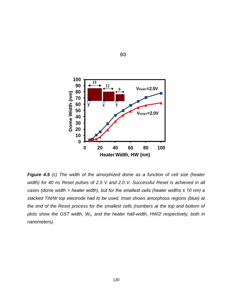
120
(c)
Figure 4.5 (c) The width of the amorphized dome as a function of cell size (heater
width) for 40 ns Reset pulses of 2.5 V and 2.0 V. Successful Reset is achieved in all
cases (dome width > heater width), but for the smallest cells (heater widths ≤ 10 nm) a
stacked TiN/W top electrode had to be used. Inset shows amorphous regions (blue) at
the end of the Reset process for the smallest cells (numbers at the top and bottom of
plots show the GST width, Wc, and the heater half-width, HW/2 respectively, both in
nanometers).
0
10
20
30
40
50
60
70
80
90
100
0 20 40 60 80 100
Do
me
Wid
th(n
m)
Heater Width, HW (nm)
VRESET=2.5V
VRESET=2.0V

121
4.3.2 The Set process in nanoscaled PCM cells
The Set process consists of re-crystallization of the amorphous region formed during
the Reset process. Such re-crystallization can occur via nucleation and growth of new
crystallites within the amorphous region and/or growth from the crystal-amorphous
boundary existing at the edge of the amorphous dome (i.e. the border between the blue
and red regions in Figure 4.2 (b) etc.). To ensure rapid crystallization, the amorphous
region should be heated to temperatures close to those at which the maximum
nucleation rate and/or crystal growth rate occurs. For GST such temperatures are
around 400oC and 550oC respectively [155, 155], considerably higher than the
crystallization temperature of around 160oC that is usually measured in ‘static’
laboratory measurements (such as via heating samples on a hot-plate, as discussed by
Friedrich et al [118] and Simpson et al in [52]), but considerably lower than the melting
temperature. Set pulse amplitudes are thus typically lower, and pulse durations longer
(to allow time for full re-crystallization to occur) as compared to Reset pulses (see
Figure 4.1). Here Set pulses in the range of 1.3 to 1.7 V in amplitude and 100 ns in
duration (with rise/fall times of 30/30 ns) were used. It was found that full re-
crystallization of the amorphous domes was achieved for all cell sizes for Set pulses
with amplitudes VSET ≥ 1.5 V.
Similar to section 4.3.1, the evolution of the crystallization process in the large
HW=100nm cell (using a 1.5V, 100ns Set pulse) is presented before the cell is scaled
down to smaller dimensions. As shown in Figure 4.6 (a), the re-crystallization of the
amorphous dome is initiated by small crystal nuclei that appear in the region above the
heater where the optimum crystallization temperature is achieved. These nuclei then
continue to grow until the whole amorphous dome is eventually crystallized. The
different colors within the amorphous dome correspond to different crystal nuclei with
different crystal orientations. The corresponding temperature distribution during the Set
process has also been shown in Figure 4.6 (b), where it can be seen that the
temperature in the region above the heater has exceeded ~650K (the temperature
required to rapidly re-crystallize the amorphous dome), and is less than the GST melting
temperature of ~893K.

122
(a)
(b)
Figure 4.6 (a) Evolution of the re-crystallization (Set) of the amorphous dome (blue)
shown in Figure 4.2 (b), using a 1.5V, 100ns Set pulse. Crystallization is initiated by
small crystal nuclei that appear in the region above the heater. The nuclei continue to
grow until the amorphous dome is fully crystallized at the end of the Set pulse. The
different colors correspond to different crystal nuclei with different crystal (plots show
one half of the GST layer and numbers at the top and bottom of plots show the GST
width Wc = 150nm and the heater half-width, HW/2 = 50nm respectively. (b)
Corresponding Set temperature distribution (at 70ns i.e. the time of occurrence of
maximum temperature) during the Set process. The Set temperature in the region
above the heater has clearly exceeded the ~650K required to rapidly crystallize the
dome, and is less than the GST melting temperature of ~893K.
Set temperature

123
Having demonstrated crystallization in the large sized cell (HW = 100nm), we now turn
our attention to the scaling of the cell. The results for a typical set of re-crystallization
simulations are shown in Figure 4.7 (a), for a Set pulse of 1.5 V and 100 ns. It can be
seen that for the larger cells re-crystallization has occurred via the nucleation (and
subsequent growth) of many new crystallites within the originally amorphous dome, but
as the cell shrinks the number of new crystallites formed is reduced until, for smallest of
cells (HW ≤ 10 nm) re-crystallization has occurred entirely via growth from the
amorphous-crystalline interface (see Figure 4.7 (b)), typically referred to as ‘interfacial
growth’. (Note: for HW ≤ 10nm, stacked TiN/W top electrodes were again used). This
change in mechanism from nucleation-dominated to growth-dominated crystallization (a
phenomenon reported in literature, e.g. [154, 155, 156] and other studies discussed in
Chapter 2) reflects both a change in temperature distributions as the cell is scaled
down, as well as the fact that for any given nucleation rate the number of crystallites
formed in a given time will be smaller in a smaller volume. Such behavior is
corroborated in Figure 4.8 (a) where the numbers of crystallites formed during the Set
process as a function of cell size (heater width) are shown for Set pulses of amplitudes
1.5, 1.6 and 1.7 V. It is observed that as the cell shrinks, the number of crystallites
formed invariably falls, and that larger Set pulse amplitudes, which lead to higher
temperatures preferentially favoring growth, also reduce the number of crystallites.
Indeed, the GCA algorithm can be used to track the nucleation and growth processes
during the entire Set process to reveal the nucleation and growth contributions to re-
crystallization in detail, as shown in Figures 4.8 (b) and 4.8 (c).

124
(a)
(b)
Figure 4.7 (a) Re-crystallization of the amorphous domes shown in Figure 4.3 and 4.5
(c) using a Set pulse of 1.5 V and 100 ns duration. (b) Evidence of interfacial growth
initiated from the amorphous-crystalline interface for HW ≤ 10 nm (inset of Fig. 4.7 (a)).

125
(a)
Figure 4.8 (a) The number of crystallites formed during the Set process as a function
of cell size (shown as heater width) and for different Set pulse amplitudes.

126
(b)
(c)
Figure 4.8 (b) and (c) The nucleation and growth rates during the Set process (1.5 V,
100 ns pulse) for a 100 nm (heater width) cell (b) and a 10 nm cell (c). It is well known
that the crystallization behaviour in PCM cells (using GST) shifts from a nucleation-
dominated behaviour to growth-dominated behaviour when cell dimensions are scaled.
A similar transition in crystallization behaviour can clearly be observed in this study,
agreeing with previously reported experimental and theoretical studies such as in [154 -
156] and other studies discussed in Chapter 2).
127
4.4 Resistance Window and Reset Current
The results of section 4.3 above show that it should, using reasonable voltages, be
possible to successfully amorphize and re-crystallize conventional phase change
mushroom-type cells scaled down to single-nanometer dimensions (specifically down to
heater contact sizes of 6 nm). What has not been considered so far is the resistance
window, i.e. the difference in resistances between the Set and Reset states, and how
this is affected by scaling. The resistance window should remain large enough to allow
for reliable differentiation on readout between the two states in the presence of noise,
cell-to-cell variability etc. In addition, the Set resistance, RSet, should not be too large
since the value of RSet affects the size of the readout current and ultimately determines
the minimum time needed to sense the state of the cell during readout (as discussed by
Jeong et al in [157]). Therefore, in Figure 4.9 the variation of cell resistance as a
function of cell size (for the results of Figure 4.3, 4.5 (a) and 4.7 (a)) is plotted. The
resistance window decreases from a factor of around 100 for the largest cells, to just
over 10 for the smallest. While such a window is still eminently usable, a larger window
would be preferable. In addition it is clear from Figure 4.9 that the absolute value of
resistance also increases as cells shrink in size, with RSet increasing from around 10 kΩ
to almost 430 kΩ. Such increases are largely due to geometric effects, since the cell
resistance scales very approximately with 1/HW (Pirovano et al [81]). The undesirable
rise in RSet and the reduction of the resistance window can be compensated for to some
degree by scaling of the heater length along with its width. For example, if the heater
length, LH (see Figure 4.1 (a)) is allowed to be reduced from the original length of 50nm
down to 10 nm for the smallest cell sizes (i.e. those with HW ≤ 10 nm), then the Set
resistance can be reduced, and the resistance window increased, as also shown in
Figure 4.9. This is because for the Set state the resistance, RH, of the heater itself
contributes very significantly to the total cell resistance and, since RH scales with heater
length LH (since RH = 4H LH/(HW)2), RSet can be reduced by shortening the heater
length.

128
Figure 4.9 Cell resistance in Set and Reset states as a function of heater contact size
(green triangles show RSET for the case of a reduced heater length of 10 nm).
0.01
0.1
1
10
0 20 40 60 80 100
Re
sis
tan
ce
(MΩ)
Heater Width, HW (nm)
RRESET
RSET
RSET
(Lh =10nm)

129
Finally attention is now turned to what is probably the main advantage of device scaling
in phase change memories, namely that as the cell size is reduced, the Reset current
should also be reduced. Since large Reset currents are one of the main drawbacks of
PCM technology at larger technology nodes (since it leads to large power consumption
and the requirement for any selector devices used in the cell array to have very high
current density capabilities), moving to smaller PCM cell sizes is a most attractive
proposition. Simple electro-thermal models (i.e. models with no phase-transformations
included) of scaling in PCM devices predict that the Reset current should scale as
1/(contact size), and experimental results on a range of product-type cell designs
(including the mushroom type) have roughly followed such a prediction, at least down to
the smallest Reset currents (~ 100 µA) so far achieved in commercial-type devices (see
Figure 4.10). The physically-realistic simulations of the performance of truly nanoscale
product-type mushroom cells in this study also show a Reset current amplitude that
scales as 1/(contact size), as shown by the (green) triangle symbols in Figure 4.10.
Indeed, it is found that the most heavily scaled mushroom cells (6 nm heater diameter)
deliver a Reset current as small as 19 µA, not so far removed from that (5 µA) obtained
by Xiong et al. for experimental, research-type (i.e. non product-oriented) cells that used
carbon nanotube (CNT) electrodes with ~ 3 nm contact diameter [109] (result also
shown in Figure 4.10). In addition, to justify the set of parameters used for the
simulations in this study, the effect of change in the thermal conductivity, k, of the active
GST material on the Reset current was also investigated using the analytical theory
presented in Section 2.2.1 and ref. [82]. We observed that varying the thermal
conductivity of GST from 0.2 – 1 W/mK had no significant effect on the Reset current,
and the resulting values lied on the green triangles shown in Figure 4.10 (hence not
repeated here). Furthermore, the relative error was calculated to be ~0.5%.
Our simulations show therefore that, with proper thermal design, the simple and
commercially-viable mushroom-type PCM cell design can indeed deliver excellent
Reset performance when scaled to single-nanometer dimensions, matching that of
much more ‘exotic’ and non-viable cell designs. Table 4.2 further shows how the Reset
current (and subsequent switching power) obtained in this study compares to other
traditional and emerging cell structures presented previously in Chapter 2 of this thesis.

130
Figure 4.10 Reset current amplitude as a function of contact size (adapted from [158])
for the mushroom-type cells of this work (triangles), for various product-type cells
reported in the literature (circles) and for the CNT-contact cell (star) reported by Xiong
et al. [109].

131
Table 4.2 A comparison of the Reset current (and power) scaling performance of
mushroom-type cells (this work) versus other reported traditional and emerging PCM
cells reviewed in Chapter 2.
PCM cell structure Contact diameter
(nm) and area
(nm2)
Reset current
(μA)
Reset
Switching
power (μW)
References
Mushroom ~ 90 (~ 6000) >1000 ~7000 Ref. [83] and
section 2.2.1
Mushroom ~ 60 (~3000) ~700 ~2200 Ref. [84] and
section 2.2.1
Nano-mushroom
(this work)
5 (~ 20)
~15 ~1 From results of
Figure 4.10
μTrench NA 600 ~3600 Ref. [88] and
section 2.2.2
μTrench ~20 (~400) 400 ~600 Ref. [84] and
section 2.2.1
Dash confined ~7.5 x 22
(127 - 165)
80-100 NA Ref. [89, 90] and
section 2.2.2
Pore-type ~40
(1250)
250 ~1500 Ref. [91] and
section 2.2.1
Pore-type ~50
(~2000)
NA NA Ref. [95] and
section 2.2.3
Crossbar 30
(~900)
160 NA Ref. [97] and
section 2.2.4
CNT-type <2
(~ 2.5)
~ 1.5 - 5 0.08 – 0.2 Ref. [109, 110,
111] and section
2.2.6

132
4.5 Chapter Summary and Conclusions
In this chapter, the scalability of non-volatile phase change memories having the
conventional mushroom-type cell architecture has been investigated, using a physically-
realistic simulation approach. It was found that such cells could be scaled successfully
down to single nanometer dimensions, specifically down to heater electrode diameters
of 6 nm and phase change layer thicknesses of 7.2 nm. However, to enable the
efficient formation of amorphous domes during the Reset process in small cells (heater
contact diameters of 10 nm or less), it was necessary to improve the thermal
confinement of the cell to reduce heat loss via the electrodes. This was performed using
a stacked, super-lattice like top electrode, but alternative approaches are also possible
(e.g. via the use of a thermal barrier layer between one or more of the electrodes and
the phase change layer). A shift in crystallization kinetics from nucleation-dominated to
growth-dominated behaviour was observed as the cell dimension were scaled, and the
crystallization for heater widths ≤ 10 nm was initiated from the crystalline-amorphous
interface i.e. interfacial growth. The resistance window between the Set and Reset
states decreased as the cell size reduced, but it was still more than an order of
magnitude even for the smallest cells and could be improved by reductions in the length
of the heater (which contributes significantly to the resistance of the cell in the Set
state). Perhaps most importantly it was found that the Reset current amplitude scaled
as the inverse of the heater contact diameter, and ultra-small Reset currents of only 19
µA (Reset powers of ~1μW) were needed to amorphize the smallest of cells, such
values being comparable to those obtained using much more ‘exotic’ (and very difficult
to manufacture) cell formats such as those using CNT electrodes.
Overall, the results reported in this chapter are very promising for the future
development of phase change memory technology as they clearly indicate (with
agreement with previously reported experimental and theoretical studies) that viable
and widely used PCM cell designs, such as the mushroom-type cell, are potentially
scalable and operable down to ultra small (sub-10nm) dimensions. This is a significant
step forward in the quest for PCM to complement or even replace existing technologies,
such as SRAM, DRAM, Flash and HDD, which have now reached their fundamental

133
scaling limitations, as discussed in Chapter 1 of this thesis. However, an important
question which still remains unanswered is whether ultrahigh storage densities (multi-
Tb/in2) can also be achieved via the scaling of PCM device structures? In this regard,
other viable cell structures, such as probe-based cells, have been widely used to
investigate storage densities in PCM, as discussed previously in Chapter 2. In the
following chapter, the scaling characteristics of patterned probe PCM (PP-PCM) cells
are investigated (using the Multiphysics Cellular Automata model) to answer this key
question regarding the potential storage capacities of PCM devices.

134
Chapter 5 Ultrahigh Storage Densities via the Scaling of Patterned Probe Phase Change Memories
In the preceding chapter, the scalability of mushroom-type PCM cells was
investigated using a physically-realistic Multiphysics Cellular Automata approach
(discussed in Chapter 3). Using this approach, it was demonstrated that
conventional PCM cells are indeed scalable and operable when scaled down to very
small (sub-10nm) dimensions, and in doing so, very low current (and power)
consumptions, comparable to those obtained using much more ‘exotic’ and non-
viable PCM cell structures, can be achieved. The simulations also enabled us to
investigate other key PCM device scaling characteristics, such as amorphization and
crystallization kinetics, thermal confinement, and Reset and Set resistance levels.
The same electro-thermal / phase change modelling approach is now used in this
chapter to answer another key question regarding the design and development of
future PCM devices i.e. can we achieve ultrahigh storage densities (multi-Tb/in2) by
the scaling of probe-based PCM cells? To answer this question, this chapter starts
off by comparing the practicability of three potential patterned probe PCM (PP-PCM)
cell structures and determines the most feasible and scalable structure for electrical
switching. The determined cell structure is then scaled down to dimensions as small
as a few nanometers, and the effect of this scaling process on potential storage
densities is investigated.
5.1 Introduction
Patterned Probe-based PCM (PP-PCM) cells, in which small phase change regions
(isolated from each other by a thermal insulator) are electrically switched using a
scanning probe (see Figure 2.18), provide an efficient approach to achieve ultrahigh
storage densities by scaling the cell dimensions. The scanning probe used to induce
electrical switching in the PP-PCM cell is essentially a sharp conductive atomic force
microscopy (C-AFM) tip (typically made out of Pt, Si, PtSi, Au etc) attached to a
cantilever, which is brought in contact with the sample surface, and then scanned

135
over the surface to write, read and erase amorphous (binary ‘0’) and crystalline
(binary ‘1’) bits, thus providing a PCM device with, ultimately, atomic resolution (see
Figure 2.17).
The review presented in Chapter 2 showed that probe-based memories have come a
long way since the first demonstration of the ‘Millipede’ system by IBM in 2002 (in
which a 2-D array of one thousand thermo-mechanical probes was used to write,
read and erase bits in a polymer medium, achieving storage densities of up to 1
Tb/in2 [99]). In phase change media, storage densities of up to 3.3 Tb/in2 (in GST
films) using thermal probe storage [100], and storage densities of up to 1.5 Tb/in2 (in
GST films) [78] and 207 Gb/in2 (in conical PP-PCM cells) [107] using electrical probe
storage have also been demonstrated, which, to our knowledge, are the highest
storage densities reported to date using phase change media (see Table 2.2).
The following sections present a detailed study of the scaling characteristics of PP-
PCM cells, using the Multiphysics Cellular Automata approach (discussed in Chapter
3 and summarized in section 4.2), and determine whether storage densities higher
than those previously reported using phase change media (~1.5 – 3 Tb/in2) can be
achieved. Moreover, the storage densities in this study are also compared to those
reported in other technologies, such as magnetic, thermomechanical and
ferroelectric probe storage (shown previously in Table 2.2).
5.2 Methodology
We start by comparing the practicability of three possible PP-PCM geometries
discussed previously in section 2.2.5; (1) Probe/DLC/GST/TiN structure previously
demonstrated by Wright et al in [78, 103] (see Figure 5.1 (a)), (2) Probe/GST/Pt
structure reported by Satoh et al in [104] (see Figure 5.1 (b)), and (3)
Probe/TiN/GST/TiN structure reported by Kim et al and Yoon et al in [106, 107]
respectively (see Figure 5.1 (c)). The starting GST material dimensions used in this
comparative study are thickness, TH = 50nm, and width, Wc = 50nm, with a 20nm
wide SiO2 isolation between each GST region. Similar to the mushroom cell study in
Chapter 4, the PCM cell is again embedded into a test bench consisting of an
electrical pulse source and an external load resistance of 10kΩ, and trapezoidal
Reset and Set voltage pulses (shown previously in Figure 4.1 (b)) of varying

136
(a) (b)
(c)
Figure 5.1 Potential PP-PCM cell structures: (a) trilayer DLC/GST/TiN cell
structure (proposed by Wright et al [78, 103]). (b) probe direct contact with GST layer
by immersing sample in an inert liquid to prevent oxidation (proposed by Tanaka et
al [104]), (c) trilayer TiN/GST/TiN cell structure (proposed by Kim et al [106] and
Yoon et al [107]).
DLC
TiN
Si substrate
Pt tip
GST SiO2
2nm
TH =
50nm
10nm
100nm
70nm
5nm
Wc=50nm 20nm
TiN
Si substrate
Pt tip
GST SiO2
5nm
70nm
TH =
50nm
10nm
100nm
Wc=50nm 20nm
Inert liquid
immersion
TH =
50nm
10nm
100nm
TiN
TiN
Si substrate
Pt tip
GST SiO2
5nm
70nm
10nm
Wc=50nm 20nm

137
amplitudes (1.0–8.0V) and durations (40-100ns) are applied to switch the cell, with
fast fall times (5 ns) in the case of the Reset pulse to facilitate the rapid cooling
needed to form the melt-quenched amorphous phase. In addition, a 5nm radius Pt
C-AFM probe is used in this study which is assumed to be stationary above the
sample surface. (Note: 5nm radius Pt C-AFM tips are the smallest commercially
available at present). For the electrical model, the boundary conditions for the cell
are again set as ‘Electrical Insulation’ for the exterior boundaries and ‘Continuity’ for
the interior boundaries, apart from the top boundary of the probe and bottom
electrode boundary (where a constant voltage is applied) which are set as circuit
terminals ‘a’ and ‘b’ respectively using the Spice Circuit Editor within COMSOL. The
thermal boundaries of the cell are again set as ‘Thermal Insulation’ for all exterior
boundaries and ‘Continuity’ for the interior boundaries. The electro-thermal material
parameters used in the simulations are listed in Table 5.1, and the phase change
modeling parameters are equivalent to those presented in [148] and section 4.2.
Table 5.1 Material parameters used for the electro-thermal and phase change
simulations [78, 148].
Element K (W/mK) C (J/ m3K) σ (Ωm)
-1
DLC 100 1.51 x 10⁶ 50
TiN 19 2.16 x 10⁶ 5 x 10
6
SiO2 1.4 3.1 x 10⁶ 1 x 10
-16
Si (substrate) 149 1.65 x 10⁶
100
Pt (probe) 71.6 2.8 x 10⁶ 0.94 x 10
7
GST (amorphous) 0.2 1.25 x 10⁶ ơ0am.exp(Δξam/KT)
[78]
GST (crystalline) 0.5 1.25 x 10⁶ ơ0crys.exp(Δξcrys/KT)
[78]

138
After determining the most practicable PP-PCM cell structure for this study, the
geometrical scaling of the determined structure is performed by reducing the TH and
Wc dimensions simultaneously. For simplicity, a constant scaling factor of TH/Wc = 1
is chosen and the GST dimensions are reduced from TH/Wc = 50/50 nm down to 5/5
nm. The storage density is then calculated using the storage density formula ρ =
1/Pint2, where Pint is the center-to-center distance between neighboring cells aligned
in a checkerboard pattern, as shown in Figure 2.18 (b).
5.3 Results and Discussion
5.3.1 Comparison of PP-PCM cell structures
A typical patterned probe PCM cell consists of a C-AFM probe and a storage media
stack consisting of the phase change regions sandwiched between a capping layer
and under layer, and isolated by insulator regions, which are deposited on a Si
substrate (as shown in Figure 5.1). The choice of top capping layer is crucial as it
not only protects the phase change layer from oxidation and wear, but also provides
a conductive path for the current required for electrical switching, and consequently
has a strong influence on the resulting temperature distributions inside the phase
change layer [78, 103]. TiN is a well-known electrode material and has previously
been used in GST-based patterned PCM cells to demonstrate electrical switching
[106, 107]. Amorphous to crystalline phase transitions in GST films as thin as 2nm
have also been reported in [52] using a trilayer TiN/GST/TiN structure. TiN is well
suited as a capping/electrode material mainly due to its suitable electrical and
thermal conductivities, and high melting temperature (~3250K). In addition, good
adhesion between GST and TiN has been observed at the atomic scale [159], and
no evidence of a reaction between TiN and GST has been reported to date.
Therefore, a cell structure consisting of a GST region isolated by a SiO2 partition,
and sandwiched between a TiN top and bottom layer seems to be a good choice for
this study. However, it is worth comparing its feasibility to two other probe-based
PCM structures presented previously in [103] and [104] before we proceed with the
geometrical scaling.

139
Cell Structure 1: DLC / GST / TiN
The cell structure proposed by Wright et al. in [103] consisted of a GST region
isolated by a 20nm wide SiO2 insulator, and sandwiched between a 2nm thick DLC
capping layer (covering the whole storage medium) and 10nm thick TiN bottom
electrode deposited on a 100nm thick Si substrate. To amorphize and crystallize bits
in the GST layer, Reset and Set pulses of 5V, 200ns and 4V, 1μs were applied
respectively using a 10nm radius PtSi scanning probe.
We now use our Multiphysics Cellular Automata model to demonstrate electrical
switching in a similar DLC/GST/TiN cell structure (50/50nm GST layer isolated by a
20nm wide SiO2 insulator), shown in Figure 5.1 (a). Using ρ = 1/Pint2, these cell
dimensions will provide a storage density of 0.13 Tb/in2 when extended to a
checkerboard pattern (see section 5.3.3). The GST layer (with a crystalline starting
phase (red in color)) is successfully amorphized using an 8V, 40ns Reset pulse
(much larger than the 2.5V, 40ns pulse used for the mushroom cells in Chapter 4),
with the amorphous bit (blue in color) formed in the region under the probe (where
the GST melting temperature of ~893 K is exceeded). The resulting Reset phase
diagram showing the amorphous bit, and the corresponding Reset temperature
distribution inside the GST layer have been shown in Figure 5.2 (a) and (b)
respectively. Following the Reset process, the amorphous bit is re-crystallized (Set)
using a 5.5V, 100ns pulse, which are shown in Figure 5.2 (a). The size and location
of the formed amorphous and crystalline bits (in the region under the C-AFM probe),
and the resulting temperature distributions, are all in good agreement with previously
demonstrated results in [103]. However, the Reset and Set voltage amplitudes
applied in this case are larger i.e. 8V for Reset and 5.5V for Set, compared to those
used previously in [103] i.e. 5V for Reset and 4V for Set. This is because faster
Reset and Set pulse durations (40ns and 100ns respectively) are used in this study
compared to the 200ns Reset and 1μs Set pulses used in [103].
Although using DLC as a capping layer presents a number of advantages, such as
good thermal stability, oxidation protection, wear resistance, and enabling successful
repeatable switching, as shown in this study and illustrated in detail in [78] and [103],
a few drawbacks currently restrict its feasibility for PCM devices:

140
Firstly, DLC has a low electrical conductivity and high thermal conductivity, which
consequently leads to larger voltage amplitudes (and therefore higher power
consumptions) required to switch the storage medium. This can be observed in
the temperature distribution in Figure 5.2 (a) where the temperature inside the
DLC layer is even higher than the temperature inside the GST layer.
Secondly, and more importantly, it has been discovered in recent years that DLC
possesses switching properties of its own, and its viability as a memory material
for resistive memory applications has been reported [160, 161].
Therefore, a PP-PCM cell structure consisting of DLC as a capping layer certainly
seems problematic for practical implementations.
Cell Structure 2: GST / TiN
The structure proposed by Satoh et al in [104] comprised a relatively thick 500nm
GST layer, with a Pt bottom electrode deposited on a Si substrate. To prevent GST
oxidation, the entire storage medium was immersed in an inert liquid (3M Fluorinert
FC-43, Ref. [105])), and a homemade Gold AFM tip was contacted directly with the
GST layer. To our knowledge, this was the first time amorphous bits were
successfully written in a crystalline GST material using C-AFM probes.
We now use our Multiphysics Cellular Automata model to demonstrate electrical
switching in a similar GST/TiN cell structure (50/50nm GST layer isolated by a 20nm
wide SiO2 insulator), shown in Figure 5.1 (b). Using the equation ρ = 1/Pint2, these
cell dimensions will provide a storage density of 0.13 Tb/in2 when extended to a
checkerboard pattern (see section 5.3.3). The GST layer (with a crystalline starting
phase (red in color)) is successfully amorphized using a 1.8V, 40ns Reset pulse
(much lower in amplitude compared to the 8.0V pulse used for Cell Structure 1, and
similar in amplitude to the Reset pulses used for the mushroom cell switching in the

141
(a)
(b)
Figure 5.2 (a) Reset and Set processes for Cell Structure 1: DLC/GST/TiN.
Successful Reset and Set achieved using 8.0V / 40ns and 5.5V / 100ns pulses
respectively. (b) Reset temperature distribution inside GST layer using an 8.0 / 40ns
Reset pulse.
50 50 50
50 50 50
Reset (8.0V, 40ns) Set (5.5V, 100ns)
T(K)
GST
Reset Temperature
DLC 1400
1000
600

142
previous chapter). Similar to Cell Structure 1, an amorphous bit (blue in color) is
formed in the region under the probe (where the GST melting temperature of 893 K
is exceeded). The resulting Reset phase diagram showing the amorphous bit and
the corresponding Reset temperature distribution inside the GST layer have been
shown in Figure 5.3 (a) and (b) respectively. Following the Reset process, the
amorphous bit is then re-crystallized (Set) using a 1.2V, 100ns Set pulse, which is
also shown in Figure 5.3 (a).
It is obvious that in comparison to Cell Structure 1, much lower pulse amplitudes are
required in this case which is a significant advantage. This is mainly because the C-
AFM probe is contacted directly with the GST layer, and no heat is lost through a
DLC capping layer. However, a liquid protective layer to prevent GST oxidation is
not practicable either as, in real devices, each cell array would have to be insulated
by immersing it in an inert liquid, making this cell structure problematic and non-
viable. Therefore, an alternative PP-PCM cell structure that not only enables
switching with lower voltages but also provides oxidation protection and wear
resistance is essential for real PCM devices.
Cell Structure 3: TiN / GST / TiN
Having highlighted the drawbacks of the DLC-based and inert liquid-based
structures, our attention is now turned to the trilayer TiN/GST/TiN PP-PCM structure
proposed by Kim et al in [106] and Yoon et al in [107], which as discussed earlier in
this section seems to be a more practicable structure for this study. The cell
structure simulated here consists of a 50/50nm GST region (isolated by a 20nm wide
SiO2 partition) sandwiched between 10nm thick TiN top and bottom electrode layers,
and deposited on a Si substrate (again corresponding to a storage density of 0.13
Tb/in2 when extended to a checkerboard pattern using ρ = 1/Pint2, see section 5.3.3).
As we are now using a top TiN capping/electrode layer, potential interference
between neighboring cells (via the top metal layer) is avoided by patterning the top
TiN metal electrode so it covers the GST layer only (and not the SiO2 insulator), as
proposed by Kim et al in [106] (see Figure 2.18 (a) and Figure 5.1 (c)).

143
(a)
(b)
Figure 5.3 (a) Reset and Set processes for Cell Structure 2: GST/TiN. Successful
Reset and Set achieved using 1.8V / 40ns and 1.2V / 100ns pulses respectively,
which are much lower in amplitude compared to the pulses used to switch Cell
Structure 1. (b) Reset temperature distribution inside GST layer using a 1.8V / 40ns
Reset pulse
50 50 50
50 50 50
Reset (1.8V, 40ns) Set (1.2V, 100ns)
400
800
1200
Reset temperatureT(K)

144
Using our Multiphysics Cellular Automata model, we manage to switch the GST layer
between the amorphous and crystalline phases using Reset and Set pulses of 1.8V,
40ns and 1.2V, 100ns respectively, with the corresponding phase diagrams shown in
Figure 5.4 (a). In this case, a rounded amorphous bit is formed a few nanometers
below the top of the GST layer, which is confirmed by the temperature distribution
inside the GST layer shown in Figure 5.4 (b). It is obvious from these simulations,
that when a conductive top metal layer is used, we can achieve repeatable switching
using low amplitude Reset and Set pulses (1.8V and 1.2V respectively), and at the
same time protect the GST layer from oxidation. Another advantage is the location
of the formed amorphous and crystalline bits which, as shown in Figure 5.3 (c) using
larger amplitude (2.5V and 1.5V) Reset and Set pulses, spreads through the
thickness of the GST layer (as opposed to being localized at the top of the GST layer
in the case of Cell Structures 1 and 2). This is encouraging for real devices as it can
potentially lead to better readout signals [162].
It is evident from the comparison study above that the trilayer TiN/GST/TiN structure
(Figure 5.1 (c)) seems to be the most practicable choice for PP-PCM devices, as
summarized in Table 5.2, and therefore is the cell structure of choice for the scaling
study in the rest of this chapter.
Table 5.2 Summary of the comparison of three potential PP-PCM cell structures
discussed in section 5.3.1.
Cell Structure 1
DLC / GST/ TiN
Cell Structure 2
GST/ TiN
Cell Structure 3
TiN / GST / TiN
Repeatable switching Yes Yes Yes
Voltage amplitudes
High
~(5 – 8 V)
Low
~(1 – 2 V)
Low
~(1 – 2 V)
Drawbacks Large voltage
amplitudes required
DLC possesses resistive
switching properties
[160, 161]
Immersion of the storage
medium in a Fluorinert
liquid to prevent GST
oxidation is impractical for
real devices
No obvious drawbacks
Practicable for real PCM
devices
No No Yes

145
(a)
(b)
(c)
Figure 5.4 (a) Reset and Set processes for Cell Structure 3: TiN/GST/TiN with
successful Reset and Set achieved using 1.8V / 40ns and 1.2V / 100ns pulses
respectively. A rounded amorphous bit is formed a few nm below the top of the GST
layer in this case. (b) Reset temperature distribution inside GST layer using a 1.8V,
40ns Reset pulse (c) Reset and Set processes in Cell Structure 3 using larger
amplitude Reset and Set pulses of 2.5V, 40ns and 1.5V, 100ns respectively.
50 50 50
50 50 50
Reset (1.8V, 40ns) Set (1.2V, 100ns)
Reset temperatureT(K)
1000
700
400
50 50 50
50 50 50
Reset (2.5V, 40ns) Set (1.5V, 100ns)

146
5.3.2 Scaling Characteristics of PP-PCM cells
In the previous section, it was shown that Cell Structure 3 consisting of a GST region
(isolated by a SiO2 insulator) sandwiched between TiN top and bottom electrodes
seems to be the most practicable structure for PP-PCM cells. In this section, our
attention is now turned to investigating the scaling characteristics of this cell
structure. For the scaling process, a constant scaling factor of 1 (as discussed in
section 5.2) is used to reduce the GST dimensions from TH/Wc = 50/50nm down to
5/5nm. It is also important to clarify here that the width of the top TiN electrode is
reduced simultaneously with reduction in the GST layer width, Wc, whilst the top and
bottom TiN electrode thicknesses (10nm for both) and the Pt probe radius (5nm) are
kept constant during this scaling process.
As discussed in previous chapters, PCM is based on reversible transitions between
an amorphous (high resistance) state and crystalline (low resistance) state of phase
change materials, with a high amplitude and short duration voltage pulse applied
during the Reset process, and a lower amplitude and longer duration pulse applied
during the Set process. It is this repeatable switching between the high resistance
amorphous state (corresponding to a binary ‘0’) and low resistance crystalline state
(corresponding to a binary ‘1’) that enables the storage of data in PCM. The
simulation results in section 5.3.1 showed that a 1.8V, 40ns Reset pulse was
sufficient to amorphize the 50/50nm GST layer (resistance shown in Figure 5.8), with
a round-shaped amorphous bit formed a few nm below the top of the GST layer (see
Figure 5.4), as opposed to being localized at the top of the GST layer in the case of
Cell Structures 1 and 2. The amorphous bit was then re-crystallized using a 1.2V,
100ns Set pulse (resistance shown in Figure 5.8), with the crystallization process
driven by the formation of crystal nuclei which nucleate and then grow until the
amorphous bit is fully re-crystallized. It will now be interesting to observe the
characteristics of the Reset and Set processes as the dimensions of the cell are
scaled down to smaller (ultimately sub-10nm) dimensions, and whether the storage
densities can be increased via this scaling process.
Figures 5.5 (a) and (b) show the Reset and corresponding Set phase diagrams as
the GST dimensions are scaled from 50/50nm down to 5/5nm using similar Reset
and Set voltage amplitudes of 1.2 – 1.8 V. The first observation for the Reset

147
process is the shape of the amorphous bit which remains circular for larger
dimensions (20nm and above), and changes to a more ellipsoidal shape (see inset
of Figure 5.5 (a)) as the GST dimensions are reduced to 10nm and below. Also, as
expected, the amorphous bit reduces in size as the GST dimensions are reduced,
with the variation in the height of the amorphous bit plotted versus the GST
dimensions in Figure 5.6. It can clearly be seen that, for each of the dimensions, we
manage to amorphize and re-crystallize the GST layer using moderate Reset and
Set voltages amplitudes.
Figure 5.7 shows the variation in the number of crystals formed during the re-
crystallization of the amorphous bits (Set process). Similar to the results in Chapter
4, a nucleation-dominated behaviour is again observed for larger dimensions, which
is indicated by the high number of crystals formed to re-crystallize the amorphous bit.
A reduction in the number of crystals is observed as the dimensions are scaled down
to smaller dimensions, indicating a transition towards growth-dominated
crystallization. It can also be seen from the inset of Figure 5.5 (b) and Figure 5.7
that a crystallization process driven by ‘interfacial growth’ from the crystalline-
amorphous boundary (similar to the results of Chapter 4) occurs as the dimensions
are reduced to 10nm and below. The similarity between the crystallization kinetics
shown in this Chapter and previously in Chapter 4 is encouraging as it shows
consistency within our Multiphysics Cellular Automata model, and also an agreement
with experimental results (for GST) discussed in Chapters 2 and 4 of this thesis.
Another important characteristic of the scaling process which must be considered is
the variation of the resistance window i.e. the difference in resistances between the
Reset and Set states, as the GST dimensions are reduced. Figure 5.8 shows the
variation of the Reset and Set resistances as a function of GST dimensions. As
expected, the resistance window decreases with reduction in GST size from
50/50nm down to 5/5nm. However, at least an order of magnitude difference
between the two states is observed even for GST dimensions as small as 5/5nm
showing that PP-PCM cells are indeed scalable and operable when scaled down to
single-nanometer dimensions.

148
(a)
(b)
Figure 5.5 (a) Successful formation of amorphous bits (shown in blue) at the end of
the Reset process as GST dimensions are scaled down in size (plots show one half
of the GST layer and numbers at the top and side show the GST thickness, TH and
width Wc. The shape of the amorphous bit changes from a rounded shape for larger
GST dimensions to ellipsoidal for smaller dimensions (shown in the inset). (b) Re-
crystallization of the amorphous bits shown in Figure 5.5 (a). Similar to the results of
Chapter 4, the crystallization for the larger GST dimensions is nucleation-dominated
(indicated by the large number of crystals formed) and is driven by ‘interfacial growth’
for the smaller GST dimensions (shown in the inset).
50
50
40
40
30
30
20
20
10
10
5
5
50
50
40
40
30
30
20
20
10
10
5
5

149
(a)
Figure 5.6 The variation in the height of the amorphous bit as a function of GST
dimensions.
(b)
Figure 5.7 The number of crystallites formed during the Set process as a function
of GST size. A transition from nucleation-dominated to growth-dominated
crystallization is observed as the GST dimensions are scaled to smaller sizes.
0
10
20
30
40
0 10 20 30 40 50
Am
orp
ho
us
bit
he
igh
t (n
m)
GST Dimensions,TH/Wc (nm)
02468
101214161820
0 10 20 30 40 50
Nu
mb
er o
f C
rys
tallit
es
GST Dimensions,TH/Wc (nm)
Nucleation-dominated
Growth-dominated

150
Figure 5.8 Cell resistance in the Reset and Set states as a function of the GST
dimensions. At least an order of magnitude difference between the Reset and Set
states is observed for the smallest cells showing that PP-PCM cells are scalable and
operable in the sub-10nm region.
0.01
0.1
1
10
0 10 20 30 40 50
Re
sis
tan
ce
(M
Ω)
GST Dimensions,TH/Wc (nm)
Reset
Set

151
5.3.3 Storage Densities in PP-PCM cells
Having determined that PP-PCM cells are scalable and operable in the sub-10nm
region, we now focus on the storage density, which is one of the most crucial
aspects in the further development of PCM technology. Furthermore, we aim to
answer the question set out at the start of this chapter i.e. can we achieve ultrahigh
storage densities via the scaling of PP-PCM devices? Also, how do these compare
to the densities achieved in other technologies, such as Thermomechanical,
Ferroelectric and Magnetic storage?
The PP-PCM cell structure we have used thus far consists of a GST region (isolated
by a 20nm wide SiO2 insulator) sandwiched between top and bottom TiN electrodes.
Using the storage density formula ρ = 1 / Pint2, where Pint is the center-to-center
distance between neighboring cells aligned in a checkerboard pattern (shown in
Figure 2.18 (b)), we can now calculate the storage density for each of the cell
dimensions from section 5.3.2.
For example, a 50/50nm GST cell plus a 20nm wide SiO2 insulator gives us a Pint
value of 70nm i.e. 25nm GST width + 25nm GST width + 20nm SiO2 = 70nm.
Therefore,
ρ = 1 / Pint2 = 1 / (70x10-9)2 = 2.04 x 10¹⁴,
as, 1 meter = 39.37 inches,
ρ = (2.04 x 10¹⁴) / (39.37)2 = 0.13 Tb / in2
The above calculations show that a storage density of 0.13 Tb/in2 can potentially be
achieved for the largest cell (50/50nm GST with 20nm wide insulator) in this study.
By applying the same calculations, we can now calculate the storage densities for
each of the scaled cell dimensions. The results for these calculations have been
shown in Table 5.3.

152
From Table 5.3, we can see that by scaling the GST dimensions from 50/50nm down
to 5/5nm (with a 20nm wide SiO2 insulator) we can potentially achieve storage
densities as high as 1.03 Tb / in2, which is extremely encouraging. However, one
aspect of cell size reduction that has not been considered yet is the reduction of the
insulator width, which should further increase the storage density significantly. To
prove this, we executed simple electro-thermal simulations for the smallest 5/5nm
cell, and determine the ultimate dimensions we can scale the insulator width down to
before potential thermal interference between cells starts taking place. The results
for these simulations have been shown in Figure 5.9 (a) – (c), where we can see that
the ultimate limit the insulator width can be reduced down to is 3nm, after which
thermal interference starts having an effect in the neighboring GST region.
(a)
(b) (c)
Figure 5.9 Electro-thermal simulations used to determine the ultimate insulator width
between GST cells before thermal interference (between cells) starts taking place.
The insulator width can potentially be reduced from 20nm (shown in (a)) down to
3nm (shown in (b)). However, for an insulator width of 1nm (shown in (c)), thermal
interference in the neighboring cell can clearly be observed.
GST 1 GST 2SiO2 insulator
5nm
5nm 5nm
5nm
20nm
GST 1
5nm
5nm
GST 2
5nm
5nm
3nm
SiO2 GST 2
5nm
5nm5nm
5nm 1nm
GST 1 SiO2

153
After scaling the insulator width from 20nm down to 3nm, the formula ρ = 1 / Pint2 can
again be used to calculate the storage density. A 5/5nm GST region with a 3nm
wide insulator gives us a Pint value of 8nm i.e. 2.5nm GST width + 2.5nm GST width
+ 3nm SiO2 = 8nm.
Therefore,
ρ = 1 / Pint2 = 1 / (8x10⁻⁹)2 = 1.56 x 10¹⁶,
as, 1 meter = 39.37 inches,
ρ = (1.56 x 10¹⁶) / (39.37)2 = 10.08 Tb / in2
The above calculations show that a storage density of ~10 Tb / in2 can potentially be
achieved in PP-PCM cells by scaling the GST dimensions down to 5/5nm (with a
3nm wide insulator). This is shown in Table 5.3, where we can see that by scaling
we can potentially enhance the storage densities from 0.13 Tb / in2 (for the largest
cell in this study) up to 10.08 Tb / in2 (for the smallest cell). These findings are very
promising as they show that storage densities much higher than the ones previously
reported in PCM electrical probe storage (1.5 Tb/in2 in [103] and 207 Gb/in2 in [107])
can potentially be achieved. In fact, the storage density of ~10 Tb / in2 reported in
this study significantly exceeds the highest storage density reported to date in PCM
i.e. 3.3 Tb / in2 reported by Hamann et al using thermal recording in [100].
It will now be interesting to see how this storage density compares to the ones
reported in other technologies, such as Thermomechanical, Ferroelectric and
Magnetic probe storage. For this, we refer back to Table 2.2, and present the
comparison in Figure 5.10 below. The bar chart clearly shows that the storage
density of ~10 Tb/in2 achieved in this study is significantly higher than the highest
storage densities of 60 Gb/in2 reported in magnetic probe storage, and 4 Tb/in2
reported in thermomechanical and ferroelectric probe storage, hence demonstrating
the potential to achieve ultrahigh (Tb/in2) storage densities in PP-PCM cells.

154
Table 5.3 Storage densities as the PP-PCM cell dimensions are scaled down to
sub-10nm dimensions.
Figure 5.10 Comparison of storage density in this work (green bar) compared to
other reported probe-based technologies (adapted from Table 2.2) [108].
0
1
2
3
4
5
6
7
8
9
10
11
Sto
rag
e D
en
sit
y (
Tb
/ in
2) Probe Storage Technologies
GST Size, TH/Wc (nm) Storage Density
50/50 (with 20nm wide SiO2) 0.13 Tb / in2
40/40 (with 20nm wide SiO2) 0.17 Tb / in2
30/30 (with 20nm wide SiO2) 0.26 Tb / in2
20/20 (with 20nm wide SiO2) 0.40 Tb / in2
10/10 (with 20nm wide SiO2) 0.72 Tb / in2
5/5 (with 20nm wide SiO2) 1.03 Tb / in2
5/5 (with 10nm wide SiO2) 2.86 Tb / in2
5/5 (with 3nm wide SiO2) 10.08 Tb / in2

155
5.4 Chapter Summary and Conclusions
In this chapter, the scalability of patterned probe phase change memory (PP-PCM)
cells was investigated using the Multiphysics Cellular Automata model. A
comparative study of three possible (and previously reported) cell structures showed
that a trilayer cell structure consisting of a GST region (isolated by a SiO2 insulator)
sandwiched between top and bottom TiN electrodes was the most suitable and
practicable structure for the scaling study when compared to two other structures; (1)
a structure consisting of diamond-like carbon (DLC) capping layer, and (2) a
structure consisting of making a direct contact between the probe and GST layer by
immersing the storage medium in an inert liquid to prevent oxidation. The main
advantages of using the TiN/GST/TiN cell structure were: (1) GST oxidation
protection via the TiN top electrode, and (2) switching between the amorphous and
crystalline states using low amplitude (1 – 2 V) Reset and Set pulses. Scaling of the
TiN/GST/TiN cell was performed by scaling the GST dimensions from 50nm down to
5nm, and in doing so amorphous bits were successfully written. Such amorphous
bits were then successfully re-crystallized with the crystallization behaviour
determined to be nucleation-dominated for larger cell dimensions and a transition to
growth-dominated behaviour was observed for smaller dimensions, with the smallest
cells crystallized by a crystallization process driven purely by ‘interfacial growth’. In
addition, the resistance window showed at least an order of magnitude difference
between the Reset and Set states predicting that PP-PCM cells are indeed scalable
and operable in the sub-10nm region. Perhaps most importantly it was found that
the storage densities could be increased as the cell dimensions were scaled, with a
storage density as high as ~10 Tb / in2 achieved in this scaling study for the smallest
cells. The storage density from this probe storage study was found to be
significantly higher than previously reported studies for PCM, and other probe-based
technologies, such as thermomechanical, magnetic and ferroelectric probe storage.
Overall, the results reported in this chapter are a significant step forward in the
development of PCM technology as they predict that probe-based PCM cells are
indeed scalable and operable in the sub-10nm region, and, in addition to low current
(and power) consumptions presented in Chapter 4 (using mushroom-type PCM
cells), ultrahigh Tb/in2 storage densities (greater than previously reported densities
for PCM) can also be achieved in nanoscaled probe-based PCM cells. Having

156
answered some key questions regarding the scalability potential of PCM devices
with some extremely encouraging and promising results, our attention in the
following chapters is now turned to some advanced functionalities of phase change
materials and devices, which, as discussed in Chapter 1, can go beyond simple two-
level memory cells. The following chapter starts off by presenting our findings
related to neuromorphic (brain-inspired) computing using PCM devices.

157
Chapter 6 Self-Resetting Spiking Phase Change Neurons for Neuromorphic Computing Applications
The preceding Chapters 4 and 5 of this thesis have focused primarily on the scaling
potential of Phase Change Memory (PCM) devices. The findings presented thus far
have shown that conventional and viable PCM devices can indeed be scaled down
to very small (sub-10nm) dimensions, and in doing so, very low current (and power)
consumptions comparable to those obtained using much more ‘exotic’ (and very
difficult to manufacture) cells can be achieved. In addition, ultrahigh (multi-Tb/in2)
storage densities (significantly higher to those for other technologies such as
Thermomechanical, Ferroelectric and Magnetic storage) can also be achieved via
the scaling of PCM devices. In addition, our sophisticated Multiphysics Cellular
Automata model has enabled us to investigate key material and device
characteristics, such as the kinetics of amorphization and crystallization, heat
confinement in PCM cells, and the variation in resistance levels between the
amorphous and crystalline states as the cell dimensions are scaled. This is a
significant step forward in achieving the ultimate goal to one day replace other
established memory technologies, such as SRAM, DRAM, Flash and HDD, and
enabling PCM to become the leading memory technology of the future.
However, as discussed previously in Chapter 1, the distinct contrast between the
Reset and Set states in phase change materials and devices can also be utilized to
achieve advanced functionalities that go beyond basic two-level memory cells. One
such functionality is Neuromorphic (Brain-inspired) Computing, which shall be
addressed in this Chapter, by utilizing the accumulation mode of operation inherent
to phase change materials and devices, to mimic the integrative properties of a
biological neuron. It is demonstrated that, by combining a PCM device with a
comparator-type external circuit, we can deliver a ‘self-resetting spiking phase
change neuron’ which can potentially open a new route for the realization of all-
phase change neuromorphic computers.

158
6.1 Introduction
The term ‘Neuromorphic Computing’ (also commonly known as Brain-inspired
Computing) was first introduced by Carver Mead in the late 1980s [163], describing
the use of very-large-scale-integration (VLSI) systems consisting of electronic
analogue circuits to mimic the neuro-biological architectures present in the nervous
system. The term has evolved over the years, and is now widely used to describe
electronic and software systems that implement models of neural systems. It is well
known that neural systems consist of two fundamental units i.e. neurons and
synapses. Neurons are excitable cells that respond to stimuli, conduct impulses and
communicate with each other, whereas synapses are the complex interconnections
that enable the communication of neurons via the transmission of electrical and
chemical signals by connecting axons and dendrites (as shown previously in Figure
1.11).
It was proposed by Stanford Ovshinsky in 2003 [164] that some phase change
materials, such as GST, should be capable of neuromorphic processing, non-binary
arithmetic processing and multi-value logic. The origin of this possibility lies primarily
in the detail of the crystallization process in nucleation-dominated phase change
materials. To date, most studies of the possible neuromorphic applications of phase
change materials and devices have concentrated on the implementation of synaptic
mimics e.g. Kuzum et al in [39] (see section 1.5.1) and Burr et al in [165], since in the
human brain synapses typically outnumber neurons by many orders of magnitude.
However, the natural accumulation property exhibited by phase change materials
(discussed in section 1.5.2) i.e. the fact that they can accumulate energy to gradually
transform from the amorphous to crystalline phase, can be exploited to also provide
a quite effective neuron mimic, as pointed out by Wright et al. in [41], and more
recently demonstrated by Tuma et al at IBM in [166]. In the neuronal-mimic mode,
the excitations provided to the phase change device are tailored in amplitude and/or
duration such that multiple input pulses, n, are needed to induce full crystallization
(rather than a single input pulse as was the case for the binary memory applications
in Chapters 4 and 5). After the receipt of a certain number of such tailored input
pulses, the resistance of the phase change cell falls below a certain pre-determined
threshold value and a neuronal output spike is generated, usually by an external
circuit. (Note: For the accumulation mode of operation, there needs to be a
159
significant difference in resistance between the n-1th pulse and the nth pulse, as
shown in Figure 1.12). In this study we use a comparator-type external circuit to
generate the neuronal spike. We also feed back to the phase change device a
portion of this output spike so the phase change cell can be Reset i.e. switched back
to the amorphous phase, and the neuronal accumulation of input excitations can
begin all over again, hence, providing a ‘self-resetting spiking phase change neuron’.
The operation of such a self-resetting phase change neuron is simulated for the first
time in this study using both physical modelling (PCM device simulations using the
Multiphysics Cellular Automata model) and SPICE circuit modelling. It is also worth
mentioning that in a biological system, a neuron typically receives between 20-100
pulses [167, 168] before the neuron fires with a firing rate in the region of 100 spikes
per second [163]. Therefore, in this study our focus is on applying up to 20 Set input
pulses to accumulate enough energy for the crystallization of the PCM cell.
6.2 Methodology
The implementation of the physical device simulations for this study consists of a
mushroom-type PCM cell with dimensions of HW = 50nm, TH = 60 and Wc = 75nm,
as shown in Figure 6.1 (a). For the electro-thermal / phase change simulations, we
use the Multiphysics Cellular Automata model along with the same electrical and
thermal boundary conditions, and pseudo-3D geometry (2D with cylindrical
symmetry), as used previously in Chapter 4. We start by amorphizing a fully
crystalline GST layer using a single 2.0V, 40ns (15ns rise/5ns fall) trapezoidal Reset
pulse (shown in Figure 6.1 (b), which forms an amorphous dome in the region above
the TiN heater (similar to the domes produced previously in Chapter 4). As the main
focus for ‘accumulation’ is on the Set (crystallization) process, the amorphous dome
is then crystallized using a pre-determined number of Set pulses n = 20, as
discussed in the previous section. After attempting simulations with varying
amplitudes and durations, a 1.025V, 70ns (20ns rise/20ns fall) trapezoidal Set pulse
(also shown in Figure 6.1 (b)) was determined to be the most optimum for the
successful implementation of a base-20 accumulator. Therefore, 20 Set pulses,
each with an amplitude and duration of 1.025V, 70ns, are applied which accumulate
enough energy to fully crystallize the amorphous dome.

160
(a) (b)
(c)
Figure 6.1 (a) Schematic of the PCM simulation cell used for the physical device
simulations with dimensions: HW=50nm, TH=60nm and Wc=75nm. (b) Trapezoidal
Reset and Set pulses used to amorphize and crystallize the PCM cell. One Reset
pulse (2.0V, 40ns), and 20 Set pulses (1.025V, 70ns each) are applied for this study.
(c) Block diagram for the self-resetting neuron SPICE circuit implementation.
50nm
60nm
50nm
50nm
150nm
50nm
GST
Wc
TH
HWSiO2
Tungsten
TiN
TiNLh
am.
cryst.
0
1
2
3
0 20 40 60 80
Vo
lta
ge
(V
)
Time (ns)
Reset (1 pulse)
Set (20 pulses)

161
The physical PCM device model then feeds into a circuit-level SPICE model (based
on the previous work of Cobley and Wright [153]) that simulates the operation of the
external neuronal spike generating circuit etc. This external circuit (shown in Figure
6.1 (c)) consists of a low-pass filter and voltage comparator for generating the output
spike, along with a feedback path that enables the output spike to also Reset the
mushroom PCM cell, hence providing the self-resetting capability. The parameters
used for the PCM device simulations are the same as those shown previously in
Table 4.1, and the SPICE circuit simulation parameters have been shown later in this
chapter in Table 6.1.
6.3 Results and Discussion
As discussed in previous chapters, ‘conventional’ binary memory is achieved by the
reversible switching between the amorphous and crystalline phases using single
Reset and Set pulses. A high amplitude and short duration electrical pulse switches
the PCM cell into the amorphous state (Reset process), and a relatively lower
amplitude and longer duration pulse switches the cell back to its crystalline phase.
In the amorphous state the PCM cell exhibits a high resistance (typically hundreds of
kΩ to MΩ), while in the crystalline state the cell exhibits a low resistance (typically
tens of kΩ), as demonstrated previously for both Reset and Set processes in this
thesis (see e.g. Figure 4.9). In the accumulation mode, the input pulse amplitudes
and/or durations are tailored to achieve the fully crystalline (Set) state (from an
amorphous (Reset) state) not with a single input pulse but with a pre-determined
number of pulses (as discussed in section 6.2). Therefore, here, we start with a fully
crystalline GST layer within the mushroom cell (shown in Figure 6.1 (a)) and apply a
single Reset pulse to form an amorphous dome within the GST layer. The
amorphous dome will then be re-crystallized during the Set process using multiple
(up to n = 20) Set pulses, as illustrated in Figure 6.1 (b)).
The application of a 2.0 V, 40ns Reset pulse forms an amorphous dome in the
region above the TiN heater (similar to the results of Chapter 4), with the evolution of
the formation of the amorphous dome shown in Figure 6.2, and the resistance at the
end of the Reset pulse i.e. after the formation of the amorphous dome is determined
to be 886 kΩ. Following the Reset process (using a single pulse), multiple Set

162
pulses of 1.025, 70ns are now applied to re-crystallize the amorphous dome, and the
change in resistance is monitored at the end of each Set pulse. The variation in the
resistance of the PCM cell as a function of the number of Set input pulses is
illustrated in Figure 6.3. A small drop in resistance of 10 kΩ is observed for the first
five pulses, which decreases the resistance from an initial value of 886 kΩ down to
872 kΩ. The resistance continues to drop very moderately for the next five pulses
i.e. from n = 5 to n = 10 pulses, with a further drop of 11 kΩ observed at the end of
the 10th Set pulse decreasing the resistance further down to 861 kΩ. This is
expected as the cell accumulates energy from each input pulse, but has not acquired
sufficient energy at this stage to fully transform the amorphous state to the crystalline
state. The resistance continues to drop moderately for the following five pulses i.e.
from n = 10 to n = 15 pulses, with the resistance after the 15th pulse determined to
Figure 6.2 Evolution of the amorphous dome (blue) formation on a fully crystalline
GST layer (red) during the Reset process. The amorphous dome is formed using a
single 2.0V, 40ns Reset pulse, and will be used for the accumulation simulations
using multiple Set pulses during the Set process. Plots show one half of the GST
layer and numbers at the top and bottom of plots show the GST width Wc = 75nm
and the heater half-width, HW/2 = 25nm respectively.

163
be 823 kΩ. However, after the 17th Set pulse is applied, it is observed that the
resistance drops more significantly (see Figure 6.3). This is because the cell has
started to acquire significantly more energy at this stage to switch the state of the
active phase change material. This is confirmed after the application of the 18th and
19th pulses where it is observed that the resistance of the cell decreases to 729 kΩ
and 558 kΩ, respectively. The results up to this point are encouraging as we have
managed to decrease the resistance of the cell moderately from a starting resistance
value of 886 kΩ down to 558 kΩ using n = 19 (1.025V, 70ns) Set pulses. However,
as discussed in Section 6.1, there needs to be a significant difference in resistance
between the n-1th pulse and the nth pulse for the accumulation process to be
accomplished successfully, and therefore, the resistance of the cell should decrease
significantly after the application of the final n = 20th Set pulse resulting in the full
crystallization of the amorphous region. This is indeed observed after the application
of the final Set pulse in this study, where the resistance is observed to decrease from
558 kΩ (after the 19th pulse) to a very small value of 36 kΩ (after the 20th pulse),
fulfilling the main condition for the accumulation mode of operation.
The phase diagrams for the Set process (corresponding to the resistance results in
Figure 6.3) have been illustrated in Figure 6.4. It can be observed that in state-1 (i.e.
after the receipt of the 1st input pulse) one or two crystal nuclei have formed in the
amorphous dome, but at this stage they have hardly any effect on the resistance of
the cell. After state-5 and state-10 (i.e. after the receipt of five and ten pulses
respectively) a few more nuclei have formed but again the cell resistance is relatively
high at this stage. After state-15 and state-18 however, it can be observed that
some of the crystal nuclei have started to grow, which results in a further decrease in
the resistance (see Figure 6.3), but even at this stage the cell has not acquired
enough energy to crystallize the amorphous dome completely. However, after state-
20 the amorphous dome has been fully crystallized, which corresponds to the low
resistance value of 36 kΩ shown in Figure 6.3.
It can clearly be observed from the results of Figure 6.3 and Figure 6.4 that there
exists a high resistance plateau region where the states (corresponding to the input
of Set pulses 1 to 17 in this case) lie below the percolation threshold (for conduction
[169]), therefore having substantially the same resistance values; nevertheless these
states remain distinct due to the fact that it takes different amounts of energy (i.e.

164
different number of subsequent pulses) to switch each different state in the plateau
region to the Set state (or to a resistance below the decision threshold). As a result,
we are not storing data in different resistance levels and are not using the same
scheme as proposed for multi-level phase change memories (e.g. Papandreou et al
[42, 43]) or for phase change based synaptic-like functionality proposed by Kuzum et
al in [39]. It is easy to see that the system of Figures 6.3 and 6.4 provides a base-20
accumulator response using a single phase change cell – each successive Set input
pulse changes the phase change cell sequentially from state 1 to 19 (state-0 being
the fully Reset state), and upon application of the 20th pulse the cell switching into
the low resistance state. It is worth mentioning that this process is non-volatile i.e. if
the power is removed from the phase change system it will remain in its existing
state, and processing can start again from where it left off when the power is re-
supplied. This accumulation study can now set the threshold for the comparator to
be used for the self-resetting capability using the SPICE model presented by Cobley
and Wright in [153].

165
Figure 6.3 The resistance of the PCM mushroom cell (shown in Figure 6.1 (a))
after the application of each of 20 Set input pulses having an amplitude of 1.025V
and being of 70ns duration (with 20ns rise and 20ns fall times). This is the basic
accumulator response, operating in this case in base-20. Set Pulses 1 – 17 have
very little effect on the device resistance, and the resistance starts to decrease more
significantly after pulse 18 and 19 (i.e. it decreases from a resistance value of 881
kΩ after the 1st pulse down to 558 kΩ after the 19th pulse). Between pulse 19 and 20
however there is a larger decrease in resistance, and at the end of the 20th pulse the
resistance drops to a very low value of 36 kΩ, which corresponds to a fully
crystallized amorphous dome (see Figure 6.4).
0
100
200
300
400
500
600
700
800
900
1000
0 5 10 15 20 25
Re
sis
tan
ce
(kΩ
)
Number of Set Pulses

166
Figure 6.4 Phase diagrams showing the crystal structures of the active region of
the PCM cell for states 1, 5, 10, 15, 18 and 20. Each of the Set input pulses has an
amplitude and duration of 1.025V and 70ns duration (with 20ns rise and 20ns fall
times). From the 1st to the 10th pulse a few crystal nuclei are formed. After the 15th
pulse the crystal nuclei have started to grow corresponding to a slight decrease in
resistance (shown in Figure 6.3). However, after the 20th pulse the dome is re-
crystallized, and the resistance value decreases to 36 kΩ (corresponding to the fully
crystallized amorphous dome).
Pulse # 1R~881kΩ
Pulse # 5R~872kΩ
Pulse # 10R~861kΩ
Pulse # 15R~823kΩ
Pulse # 18R~729kΩ
Pulse # 20R~36kΩ
167
The natural accumulation process inherent to phase change materials and devices
presented so far can now be used to provide a form of ‘spiking’ and ‘self-resetting’
neuronal mimic by connecting the PCM cell to the low-pass filter/comparator circuit
shown in Figure 6.1 (c). For example, the PCM cell in this circuit accumulates
energy from incoming pulses and fires (i.e., switches to a low resistance state),
causing the comparator to generate an output spike, only after a certain number of
pulses are applied. The feedback path within the circuit can then enable the output
spike to also Reset the mushroom PCM cell, hence providing the self-resetting
capability for the neuron.
The SPICE circuit model of Cobley and Wright has been described in detail in [153],
and a brief description has been provided here. Figure 6.5 (a) shows a block
diagram of the model which comprises of four major sub-blocks, namely an input
detection module, Z-model module, memory module and control module. Note that
the current source circuit in Figure 6.5 (a) provides the input signals for the PCM cell
and comprises simply a set of program and read current generators. For
conventional binary operation, the input detection module is designed to detect an
input programming or read current pulse, applied to the PCM cell and generate as its
output an appropriate input voltage for the memory module. The input detection
module outputs two voltage states corresponding to fully crystallized and
partially/fully amorphized states respectively, along with a voltage output that sets
the amorphous resistance value. When used for multilevel operation, as
demonstrated in [153], the input detection module additionally detects the
intermediate programming current amplitudes and outputs a voltage for the
appropriate partially amorphous resistance value. The memory module uses the two
output voltages from the input detection module to select, via the Z-model module,
the programmed state of the cell as crystalline or amorphous / partially amorphous.
During static current-voltage simulations, a feedback signal from the control module,
also switches the internal memory to the crystalline state. The Z-model module
provides the final PCM cell resistance appropriate to the programming conditions
and to any time delay between programming and reading [153].
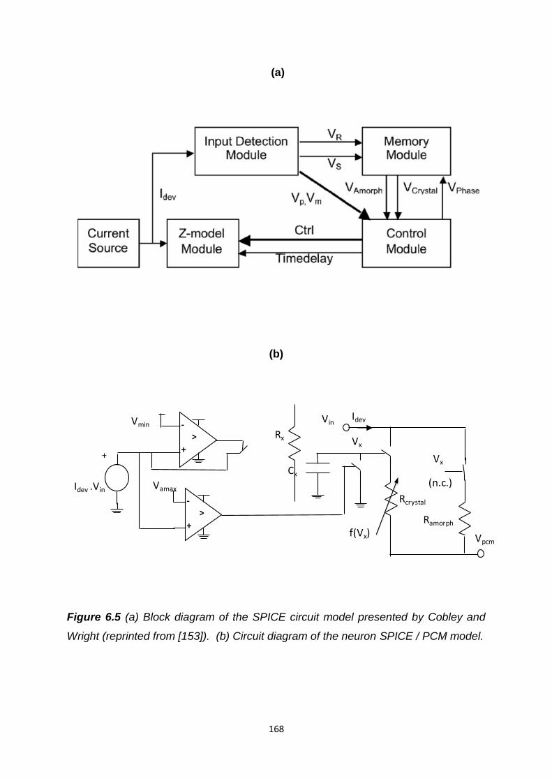
168
(a)
(b)
Figure 6.5 (a) Block diagram of the SPICE circuit model presented by Cobley and
Wright (reprinted from [153]). (b) Circuit diagram of the neuron SPICE / PCM model.
Vx
Cx
Rx
(n.c.)
Idev-
>
+
Ramorph
Rcrystal
Vpcm
Vin
Idev .Vin
+
Vmin
Vamax
->
+
Vx
f(Vx)
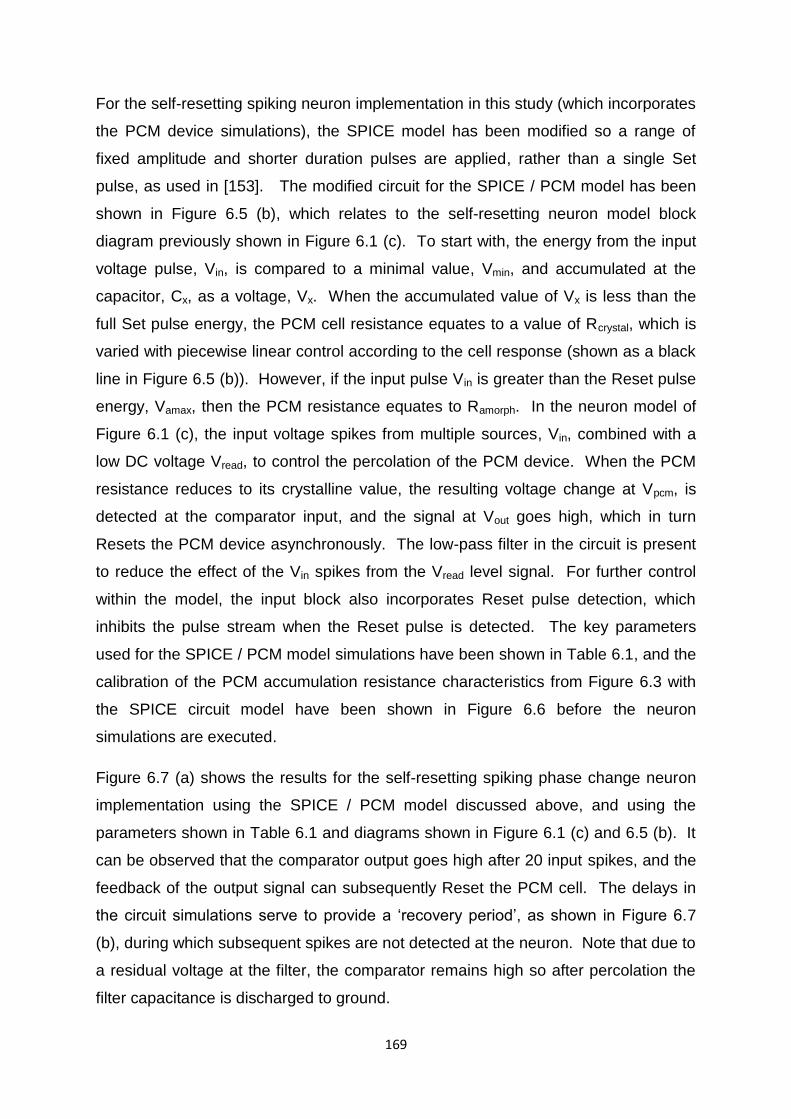
169
For the self-resetting spiking neuron implementation in this study (which incorporates
the PCM device simulations), the SPICE model has been modified so a range of
fixed amplitude and shorter duration pulses are applied, rather than a single Set
pulse, as used in [153]. The modified circuit for the SPICE / PCM model has been
shown in Figure 6.5 (b), which relates to the self-resetting neuron model block
diagram previously shown in Figure 6.1 (c). To start with, the energy from the input
voltage pulse, Vin, is compared to a minimal value, Vmin, and accumulated at the
capacitor, Cx, as a voltage, Vx. When the accumulated value of Vx is less than the
full Set pulse energy, the PCM cell resistance equates to a value of Rcrystal, which is
varied with piecewise linear control according to the cell response (shown as a black
line in Figure 6.5 (b)). However, if the input pulse Vin is greater than the Reset pulse
energy, Vamax, then the PCM resistance equates to Ramorph. In the neuron model of
Figure 6.1 (c), the input voltage spikes from multiple sources, Vin, combined with a
low DC voltage Vread, to control the percolation of the PCM device. When the PCM
resistance reduces to its crystalline value, the resulting voltage change at Vpcm, is
detected at the comparator input, and the signal at Vout goes high, which in turn
Resets the PCM device asynchronously. The low-pass filter in the circuit is present
to reduce the effect of the Vin spikes from the Vread level signal. For further control
within the model, the input block also incorporates Reset pulse detection, which
inhibits the pulse stream when the Reset pulse is detected. The key parameters
used for the SPICE / PCM model simulations have been shown in Table 6.1, and the
calibration of the PCM accumulation resistance characteristics from Figure 6.3 with
the SPICE circuit model have been shown in Figure 6.6 before the neuron
simulations are executed.
Figure 6.7 (a) shows the results for the self-resetting spiking phase change neuron
implementation using the SPICE / PCM model discussed above, and using the
parameters shown in Table 6.1 and diagrams shown in Figure 6.1 (c) and 6.5 (b). It
can be observed that the comparator output goes high after 20 input spikes, and the
feedback of the output signal can subsequently Reset the PCM cell. The delays in
the circuit simulations serve to provide a ‘recovery period’, as shown in Figure 6.7
(b), during which subsequent spikes are not detected at the neuron. Note that due to
a residual voltage at the filter, the comparator remains high so after percolation the
filter capacitance is discharged to ground.

170
Table 6.1 Key parameters used for the self-resetting spiking phase change
neuron simulations using the SPICE / PCM model (shown in Figures 6.1 (c) and 6.5
(b)). The PCM device results from Figure 6.3 and 6.4 are used as an input for the
SPICE model to carry out the simulations.
Figure 6.6 Calibration (dotted line) of the SPICE circuit model with the PCM
device results from Figure 6.3.
0 5 10 15 20
Number of Set pulses
1000
800
600
400
200
0
Re
sis
tan
ce (kΩ
)
Parameter name Description Value
Rcrystal Crystalline resistance 36 kΩ
Ramorph Amorphous resistance 886 kΩ
Vpulse Percolation pulse amplitude for neuron 1.025 V
Vmax Percolation threshold (filtered) 38 mV
Vam Min amorphous pulse at 20ns width 1.9 V
Vread Read pulse amplitude for neuron 0.1 V
Baseref Base for pulse Vref 20
Rf.Cf Low-pass filter time constant for neuron 0.01 ms
Vamax Percolation energy equivalent of neuron 74 μV
Rload Load resistance for neuron 442 kΩ
Tpmin Effective pulse width for rise and fall time above Vpmin 2.5 ns
Vref1 Value for max total energy at Vx 643.9n
Vpmin Minimum detected percolation pulse 1.0 V

171
(a)
(b)
Figure 6.7 (a) Simulated response for the self-resetting spiking phase change
neuron implementation. Input spikes are shown in green and output spikes are
shown in red. (b) Simulated response showing the worst case ‘recovery period’
(black arrow). During this period subsequent spikes are not detected at the neuron.
2.0
1.5
0.5
1.0
0
Vo
lta
ge
(V
)
50 100 150 2000
Time (μs)
1.0
2.0
0
164.8 165.3
Vo
lta
ge
(V)
Time (μs)

172
From the overall findings presented in this chapter, it is clearly evident that phase
change neurons can indeed be designed and developed by utilizing the natural
accumulation process inherent to phase change materials and devices. As
discussed by Tuma et al in [166], artificial neuromorphic systems based on
populations of spiking neurons are a valuable tool in understanding the human brain
and in the construction of neuromimetic computational systems, and in this regard,
progress on the realization of neurons for phase change neuromorphic computing
has so far been lacking. Our findings in this chapter have aimed to address this
shortcoming by combining physical PCM device simulations with SPICE circuit
modelling to implement phase change biological neurons that can not only generate
spikes but can also be Reset, thus opening a potential route for the realization of all-
phase change neuromorphic computers.
6.4 Chapter Summary and Conclusions
Neuromorphic, or Brain-inspired, computing applications of phase change devices
have to date concentrated primarily on the implementation of phase change
synapses. However, by using the so-called accumulation mode of operation
naturally inherent to phase change materials, phase change devices can also be
used mimic the integrative properties of a biological neuron. In this chapter, we have
demonstrated, using both physical and circuit modelling, that by combining a
nanoscale PCM device with an external SPICE circuit we can deliver a ‘self-resetting
spiking phase change neuron’, which can potentially open a new route for the
realization of all-phase change neuromorphic computers.
The PCM device simulations were performed using a mushroom-type PCM cell
along with the Multiphysics Cellular Automata approach used in previous chapters of
this thesis. For the accumulation work in this study, the mushroom cell was initially
Reset using a moderate 2.0V / 40ns pulse to form an amorphous dome in the region
above the heater, which resulted in a high Reset resistance value of 886 kΩ. The
amorphous dome was then re-crystallized using n = 20 Set pulses (with each pulse
having an amplitude of 1.025V and duration of 70ns). During the Set process, the
cell accumulated energy from each Set pulse until it acquired enough energy (by the
end of the 20th pulse) to switch the cell to the crystalline state, with the final Set
173
resistance value determined to be 36 kΩ. Most importantly, a significant difference
in resistance levels between the 19th (n-1th) and 20th (nth) Set pulse was observed
(i.e. 558 kΩ and 36 kΩ respectively), hence fulfilling the main requirement for the
accumulation mode of operation, and thus providing a ‘base-20 phase change
accumulator’ for the phase change neuron simulations. The PCM device model was
then combined with a SPICE circuit model consisting of a low-pass filter / comparator
circuit for generating the neuron output spike, along with a feedback path that
enabled the output spike to Reset the PCM cell, hence providing the self-resetting
capability. It was observed that the comparator output switched to high after 20 input
spikes, and the feedback of the output successfully Reset the PCM cell, hence
delivering a ‘self-resetting spiking phase change neuron’. As shown by Tuma et al in
[166], even such a simple computation ‘primitive’ can carry out surprisingly complex
neuromorphic computational tasks.

174
Chapter 7 Electrical Switching in Phase Change Metadevices for Near-infrared Absorber and Modulator Applications
In the preceding chapter, we demonstrated, by combining physical nanoscale PCM
device simulations with an external comparator-type circuit, and utilizing the natural
accumulation process inherent to phase change materials and devices, that a ‘self-
resetting spiking phase change biological neuron’ can be delivered, potentially
opening a new route for the realization of all-phase change neuromorphic computers
of the future. It is evident from the findings presented in this thesis so far that our
Multiphysics Cellular Automata approach can be applied successfully to not only
address binary phase change memory applications (down to dimensions as small as
a few nm) but also address novel applications that go beyond two-level memory,
such as neuromorphic computing. In doing so, our modelling approach has enabled
us to investigate some key phase change material and device characteristics, such
as current and power consumptions, storage densities, amorphization and
crystallization kinetics, thermal confinement, Reset and Set resistance levels, and as
demonstrated in the previous chapter, the implementation of a base-20 accumulator
for the simulation of biological neurons. The findings presented so far have also
been in good agreement with previously published experimental and theoretical
studies, showing that the Multiphysics Cellular Automata approach can indeed
produce physically realistic simulation results.
In this chapter, we now turn our attention to another novel application of phase
change materials i.e. phase change metadevices, a topic that was introduced
previously in section 1.5 of this thesis. Here, our main focus is on demonstrating
‘electrical switching’ (using our Multiphysics Cellular Automata approach) in
practicable phase change metadevices for absorber and modulator applications,
which are suited to operation in the technologically important near-infrared range of
the spectrum, specifically here 1550nm.

175
7.1 Introduction
Thin-film electromagnetic absorbers have a number of important applications in the
infrared and visible part of the spectrum including infrared detection [170], solar
energy harvesting [171] and refractive index sensing [172]. Similarly, thin-film light
modulating devices are much in demand for optical communications, optical signal
processing and spatial light modulator applications, as discussed in section 1.5.3
[46]. In this chapter, the switching characteristics of novel forms of electromagnetic
absorbers and modulators that combine metamaterial arrays with switching phase
change films are presented. As discussed in previous chapters of this thesis, the
properties of phase change materials, such as GST, differ considerably between the
amorphous and crystalline phases, and this contrast between the two phases can be
utilized for non-volatile memory (Chapters 4 and 5), neuromorphic computing
(Chapter 6), and also for the provision of solid-state and flexible displays as
demonstrated recently by Hosseini et al in [173]. By including such phase change
materials into a metamaterial resonator structure, the properties in the environment
of the resonator can be modified according to the state of the phase change
material, thus yielding an active device suited to, for example, an electrically or
optically controlled (switched) modulator. Such a modulator structure is shown
schematically in Figure 7.1 (a) below, which consists of a 4-layer arrangement
comprising a bottom metal layer, the GST phase change layer, an ITO layer and a
patterned top metal layer (here patterned into strips). The simulated reflectance
spectrum of this modulator structure, with the GST layer in both amorphous and
crystalline phases, and optimized for maximum modulation depth (MD) of 1550nm, is
also shown in Figure 7.1 (b) (refer to ref. [177] for details of the modulator design
and sensitivity analysis).
Phase change metadevices so far reported in the literature have generally been
switched ex-situ using fast, high-power external lasers, or simply by carrying out
thermal annealing in an oven to induce a one-way transition from the amorphous to
the crystalline phase (due to the fast cooling requirements, oven annealing cannot
be used to form the amorphous phase) [46, 174]. For real-world applications
however, some form of in situ switching of the phase change layer would be most

176
(a) (b)
Figure 7.1 (a) Schematic of a GST-based thin film phase change metamaterial
absorber/modulator structure (inset shows the top metal layer patterned into
squares). (b) Simulated reflectance spectrum for the design in Fig. 7.1 (a) with Au
top and bottom metal layers and with the phase change GST layer in both crystalline
and amorphous states. The design was optimized for maximum modulation depth
(MD) of 1550nm. (Reprinted from [177]).
attractive. In our case, this might be achieved by dividing the metal-dielectric-
chalcogenide-metal absorber/modulator structure of the form shown in Figure 7.1
into an arrangement of pixels, each of which could be separately excited electrically
in order to switch the phase change layer (for example, in the case of a modulator
with the topmost metal layer patterned into strips, one might also pattern the bottom
metal layer into (orthogonal) strips, yielding a structure electrically similar to the
crossbar structures discussed in section 2.2.4, in which individual ‘cells’ are
addressed by appropriate excitations being placed on the relevant intersecting strips
– the so called ‘bit’ and ‘word’ lines in memory device terminology.
7.2 Methodology
We simulate electrical switching in the structure shown in Figure 7.1 by assuming
each pixel is represented by the unit-cell of the form shown in Figure 7.2 (a). The
cell structure consists of a GST layer (with dimensions TH = 68nm and Wc = 585/2 =
287.5nm) sandwiched between a 5nm thick ITO layer and 80nm thick Gold (Au)

177
bottom electrode. The top metal strip consists of an Au layer (with a width of 381nm
(half-width of 190.5nm)), and a Ti layer (with 5nm thickness) is also used to provide
adhesion. Similar to the simulations in previous chapters of this thesis, we use our
Multiphysics Cellular Automata approach along with the same electrical and thermal
boundary conditions (as used in previous chapters) for the simulations in this study.
A pseudo-3D (2D with cylindrical symmetry) geometry is again used, and the cell is
embedded into a virtual test bench consisting of a 1 kΩ series load resistor and a
voltage source. To achieve electrical switching, we apply trapezoidal Reset and Set
pulses of 2.4V, 50ns (15ns rise, 5ns fall) and 1.4V, 100ns (30ns rise, 30ns fall) as
shown in Figure 7.2 (b). The electro-thermal and phase change parameters used for
the simulations in this study have also been shown in Table 7.1.
(a) (b)
Figure 7.2 (a) Schematic of the phase change metamaterial absorber/modulator
structure showing the dimensions of each material. A GST layer with thickness, TH
= 68nm, and width, Wc = 287.5nm is used. (b) Trapezoidal Reset and Set pulses of
2.4V, 50ns and 1.4V, 100ns are applied to switch the GST layer between the
amorphous and crystalline phases.
381nm
Au 30nm
5nm
5nm
68nm
80nm
100nm
575nm
Ti
ITO
GST
Au
Si (substrate)
Wc
TH
0
1
2
3
0 20 40 60 80 100
Vo
lta
ge
(V
)
Time (ns)
Reset
Set

178
Table 7.1 Material parameters for the electro-thermal / phase change simulations
[78, 148].
7.3 Results and Discussion
The following sub-sections 7.3.1 and 7.3.2 present the results and discussion for the
simulation work in this study. In 7.3.1, a discussion on the choice of layers for the
absorber/modulator structure is presented, followed by the outcomes of the Reset
and Set process simulations presented in 7.3.2.
7.3.1 Choice of material layers for Modulator structure
The modulator structure shown in Figure 7.1 consists of a phase change (GST) layer
sandwiched between a bottom metal layer, an ITO layer, and a patterned metal layer
(here patterned into strips); on switching of the state (from amorphous to crystalline
or vice-versa) of the phase change layer, the intensity of the light reflected from the
structure is modulated. Although the main focus of this chapter is on electrical
switching, it is important to consider the optical feasibility of such a structure as well
before the electrical switching results are presented.
While, for this study, we concentrate on the use of GST as the phase change
medium (due to its attractive and well-understood properties and behaviour, and in
light of the promising results presented in previous chapters of this thesis), it is worth
mentioning that other non-chalcogenide phase-switching materials, such as VO2
Element K (W/mK) C (J/m3K) σ (Ωm)
-1
Au 310 2.48 x 10⁶ 44 x 10
6
ITO 11 2.42 x 10⁶ 8.3 x 10
3
Ti 7.5 3.19 x 10⁶ 7.4 x 10
5
GST (amorphous) 0.2 1.25 x 10⁶ ơ0am.exp(Δξam/KT)
[78]
GST (crystalline) 0.5 1.25 x 10⁶ ơ0crys.exp(Δξcrys/KT)
[78]
Si (substrate) 149 1.65 x 10⁶ 100

179
(with its large refractive index change when heated to switch it from its insulating
metal phase [175]), could potentially be used. However, the phase transition in VO2
is volatile (the material returning to its insulating phase on cooling), whereas in a
phase change material like GST it is non-volatile, meaning that any particular
(amorphous or crystalline) phase can be maintained without the requirement for
input power – a particularly attractive feature in terms of device performance.
Previous work on GST-metamaterial structures has concentrated on the mid-infrared
part of the spectrum, with applications such as improved energy absorption in optical
memories [47] or tunable photonic crystals [176], but the near-infrared (NIR) region
has remained largely under-explored, due perhaps to the fact that optical losses in
GST start to rise appreciably in that region. However, operation in the NIR region is
important since the most commonly used wavelengths for optical communications
and optical signal processing lie in this region, specifically between 1530nm to
1565nm for the conventional C-band. Furthermore, in previous studies, the
requirement to protect the active phase change layer from the effects of oxidation
appears to have been largely ignored. The properties of phase change thin films are
known to deteriorate rapidly on exposure to air (as highlighted in Chapter 2), and so
for practicable absorber or modulator designs the phase change layer should be
encapsulated by a protecting layer that, to maintain optical access and to allow for
the possibility for electrical switching, should ideally be optically transparent and
electrically conductive [173]. For this work, ITO is used to provide such a layer.
In terms of the choice of the composition of the (top and bottom) metal layers, gold
and silver are usually metals of choice in the literature, since they have an excellent
plasmonic behaviour. However, Ag is particularly diffusive, especially at the high
temperatures experienced during the switching of the phase change layer, and is
thus best avoided. Aluminium has also been suggested as an alternative for the
metal layers [174]. But the melting point of Al (at ~660oC) is relatively low, and in
particular is very close to that (~620oC) of GST we use here. Since to amorphize the
GST layer we need to heat it to above its melting temperature (followed by fast
cooling), there is a danger that the top Al metal layer in particular would also melt
(and, without any encapsulation), and so the use of Al, at least with GST seems
problematic. TiN and W are also potential candidates for use as top and metal
layers, and, as demonstrated in Chapters 4, 5 and 6, are well suited for electrical

180
switching. However, when simulated for their optical feasibility (results shown in ref.
[177]), it was found that excellent absorber/modulator performance could be
obtained if TiN and W were used for the top metal layer only, but not if used for both
top and bottom metal layers. This was explained by considering the absorber as a
periodic structure capable of adding momentum to the incoming radiation in the
horizontal direction, a process that requires the bottom metal layer to be one that
exhibits excellent plasma behaviour, such as Au (or Al), in order to obtain near zero
reflectance with the phase change layer in the amorphous phase. Therefore, in light
of the above discussions, the choice of Au for the top metal strip and bottom
electrode seems to be the most practicable choice for this study (due to its high
melting point (~1060oC), and when taking both electrical and optical switching
possibilities into consideration).
7.3.2 Electrical Switching
Having discussed the pros and cons of some of the materials that can potentially be
used for the absorber/modulator structure to be simulated, and deducing that the
Au/ITO/GST/Au structure shown in Figure 7.2 (a) is indeed the most practicable
choice for this study, we turn our attention to the electrical switching of this structure.
Similar to results presented in previous chapters, we again start with a fully
crystalline GST layer and amorphize it using a high amplitude and short duration
electrical pulse. For this structure, a 2.4V, 50ns (15ns rise, 5ns fall) Reset pulse was
determined to be sufficient to fully amorphize the GST layer (from a crystalline
starting phase), when applied between the top and bottom metal layers. Typical
results are shown in Figures 7.3 and 7.4, here for the case of Au top and bottom
metal layers (although similar results were obtained for Al, W and TiN). In Figure 7.3
(a) we show the Reset temperature distribution in the unit cell at the time when the
maximum temperature occurs (i.e. 45ns in this case). We observe that the
maximum temperature does indeed exceed the melting point of GST (620oC or 893
K), and the temperature distribution is relatively uniform throughout the GST layer.
We also note that the temperature experienced by the top metal layer is also
relatively high in this case (~980 K), precluding the use of aluminium (melting point of
~933 K) for the top layer, as discussed in sub-section 7.3.1 (replacing the top Au

181
layer with Al in the simulations shown in Figure 7.3 did not significantly affect the
maximum temperature reached). As a result of the applied Reset pulse, we
managed to amorphize the GST layer with the resulting phase diagram shown in
Figure 7.4 (a). It can be observed that the temperature uniformity within the GST
layer has led to the GST layer amorphizing completely from a crystalline starting
phase (from red to blue in Figure 7.4).
To achieve successful crystallization, a lower amplitude and longer duration Set
pulse must be applied between the top and bottom metal layers. In this case, a
1.4V, 100ns (30ns rise, 30ns fall) Set pulse was determined to be sufficient to re-
crystallize the fully amorphous GST layer. In Figure 7.3 (b), we show the Set
temperature distribution in the unit cell at the time when the maximum temperature
occurs (i.e. 70ns in this case). We observe that the maximum temperature
experienced by the GST layer is in the region of 720K or 447oC, a typical value
required to ensure rapid (on the order of tens of nanoseconds) crystallization of GST,
as shown in previous chapters of this thesis. In addition, the temperature distribution
is again relatively uniform throughout the GST layer, which subsequently crystallizes
the fully amorphous GST layer (as shown in Figure 7.4). Similar to the crystallization
results presented in previous chapters, we again observe the formation of crystal
nuclei (with different colours representing different crystal orientations) in the
amorphous GST layer, which grow after being formed until the GST layer is
completely crystallized. We also observed that the fully crystalline GST layer could
also be re-amorphized again by the application of the 2.4V, 50ns Reset pulse used
to amorphize the GST layer in the first case.
Thus it would appear, at least from a simulation perspective (and for the material
properties shown in Table 7.1), that phase change metadevices of the form shown in
Figure 7.1 would indeed be suited to in situ electrical switching of the phase change
layer, so providing a readily active / tunable / reconfigurable photonic response. It
was also noted during this study that, to avoid any possible concerns of gold
diffusion from the bottom metal layer into the GST layer (as pointed out in ref. [46]),
an additional ITO layer can be inserted on top of the bottom Au layer without any
detrimental effects, in an appropriately optimized structure, on the overall electrical
or optical performance.

182
(a)
(b)
Figure 7.3 Simulated temperature distribution in the structure of Figure 7.2 (a) for
the case of electrical excitation (assuming an electrically pixelated structure with
pixel size equal to the unit-cell size) for (a) a Reset pulse of 2.4V, 50ns and (b) a Set
pulse of 1.4V, 100ns respectively.
Au
Ti ITO
GST
Au
1000
900
800
T(K)
Reset Temperature
Au
Ti ITO
GSTAu
720
630
540
T(K)
Set Temperature

183
Figure 7.4 The starting and finishing phase states of the GST layer after a sequence
of Reset / Set / Reset electrical pulses: the GST layer starts in a fully crystalline state
(shown in red); after the application a first 2.4V, 50ns reset pulse the GST layer is
fully amorphized (shown in blue); after the application of a 1.4V. 100ns Set pulse the
GST layer is fully re-crystallized (into a number of crystallites, as shown by the
different colours); finally after the receipt of a second Reset pulse, the GST layer is
fully re-amorphized.
Reset process
Set process
Reset process

184
7.4 Chapter Summary and Conclusions
In summary, it has been shown in this chapter that it is feasible to design phase
change metadevices for absorber and modulator applications and suited to operation
in the technologically important near-infrared range of the spectrum (specifically
1550nm in this case). Furthermore, we have discussed that it is possible to design
such devices using a practicable approach providing environmental stability by
incorporating an ITO layer to protect the GST layer from oxidation while still allowing
electrical access. From the discussions in this chapter, it was also deduced that a
structure consisting of the GST layer sandwiched between an Au bottom electrode
and Au top metal strip was the most practicable solution (for both electrical and
optical switching) in comparison to using Al, TiN and W as both top and bottom metal
layers. Finally, we have shown (using our Multiphysics Cellular Automata approach)
that pixelated versions of such phase change metadevices can indeed be switched
repeatedly between the amorphous and crystalline states by in situ electrical
excitation using pulsing regimes similar to those used in phase change memory
device applications presented in preceding chapters of this thesis.

185
Chapter 8
Non-Arrhenius Kinetics of Crystallization in Phase Change Materials
In the preceding chapters of this thesis, our focus has been on the scaling and
advanced functionality potential of phase change materials and memory devices. So
far, from the results and discussions in Chapters 4 and 5, we have shown that viable
PCM devices can indeed be scaled down to extremely small (sub-10nm)
dimensions, and in doing so extremely low current (~μA)/power consumptions (~μW)
and ultrahigh storage densities (Tb/in2) (matching or exceeding those of other
technologies) can potentially be achieved. In addition, in Chapters 6 and 7, we have
managed to successfully address some novel applications of phase change
materials that go beyond two-level binary memory, such as neuromorphic computing
and phase change metadevices, with promising results.
It is evident from the findings presented so far, that the Gillespie Cellular Automata
(GCA) phase change model (combined with electro-thermal simulations) can be
used to address a variety of different aspects related to phase change materials and
memory devices, and in doing so, physically realistic results can indeed be obtained.
However, one last aspect worth considering and investigating before we conclude
this thesis is whether our phase change model can replicate recent experimental and
theoretical results revealing that crystallization properties such as crystallization
temperature and crystallization time may actually differ in phase change materials,
such as GST, from the simple Arrhenius-type behaviour, thus providing evidence for
non-Arrhenius kinetics of crystallization. In this chapter, we use the Gillespie Cellular
Automata model (discussed in detail in Chapter 3) to study this non-Arrhenius type
behaviour.
8.1 Introduction
Phase change materials, such as GST, possess different properties in the Reset
(amorphous) and crystalline (Set) states, and these contrasting properties are used
for data storage and memory applications, as has been discussed over the course of

186
this thesis. The transition to the amorphous state is achieved via Joule heating
induced melting and fast quenching, and is typically operated in a short time. On the
other hand, the transition to the crystalline state is achieved in a longer time via the
nucleation and growth of crystalline grains in the amorphous phase change material.
To reduce the crystallization time and design new phase change materials with
faster switching speeds, a good understanding of the crystallization kinetics is
required. In this regard, our sophisticated GCA phase change model has enabled us
to address some key aspects related to the crystallization of phase change materials
over the course of this thesis. However, one material parameter related to the
kinetics of crystallization which must also be discussed is the ‘activation energy’, Ea,
(a term first introduced by Swedish scientist Svante Arrhenius in the late 1880s, and
typically defined as the maximum energy required to start a chemical reaction [178]).
Ea (typically measured in units of electron-volts (eV)) has a direct effect on the
crystallization speed of phase change materials [179] i.e. materials with lower Ea
values typically crystallize with faster speeds compared to materials with higher Ea
values (e.g. Ge2Sb2Te5 (GST) has a typical measured Ea value ranging between 2.0
– 2.6 eV [77, 179, 180] whereas Ge4Sb1Te5 has a typical Ea value of 3.7 eV [180],
and therefore Ge2Sb2Te5 will inevitably have a faster crystallization time compared to
Ge4Sb1Te5). The crystallization time, tx, typically decreases with the crystallization
temperature T according to an Arrhenius behaviour, as follows [179]:
(8.1)
where Ʈo is a pre-exponential factor, Ea is the activation energy for crystallization
(typically ranging from 2 – 2.6 eV for GST), and kB is the Boltzmann constant.
Recent studies however, (e.g. Orava et al [181], Ciocchini et al [179], Jeyasingh et al
[182] to name a few) have shown that GST in fact exhibits different activation
energies at different crystallization temperatures, thus providing evidence for non-
Arrhenius kinetics of crystallization. This has been illustrated by the Arrhenius plot
(from [179]) in Figure 8.1 where we can observe that Ea exhibits its well known value
of ~2 - 2.6 eV at lower crystallization temperatures, but at higher temperatures a
lower value of ~0.5 eV is observed.
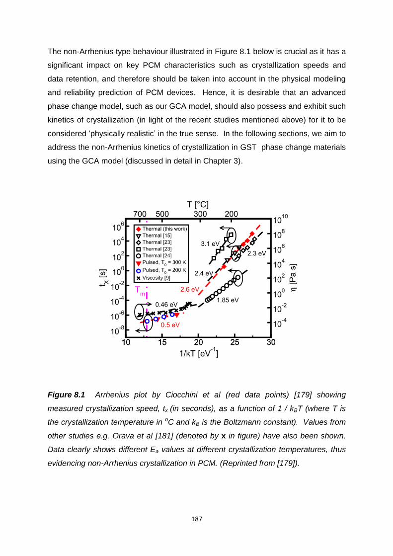
187
The non-Arrhenius type behaviour illustrated in Figure 8.1 below is crucial as it has a
significant impact on key PCM characteristics such as crystallization speeds and
data retention, and therefore should be taken into account in the physical modeling
and reliability prediction of PCM devices. Hence, it is desirable that an advanced
phase change model, such as our GCA model, should also possess and exhibit such
kinetics of crystallization (in light of the recent studies mentioned above) for it to be
considered ‘physically realistic’ in the true sense. In the following sections, we aim to
address the non-Arrhenius kinetics of crystallization in GST phase change materials
using the GCA model (discussed in detail in Chapter 3).
Figure 8.1 Arrhenius plot by Ciocchini et al (red data points) [179] showing
measured crystallization speed, tx (in seconds), as a function of 1 / kBT (where T is
the crystallization temperature in oC and kB is the Boltzmann constant). Values from
other studies e.g. Orava et al [181] (denoted by x in figure) have also been shown.
Data clearly shows different Ea values at different crystallization temperatures, thus
evidencing non-Arrhenius crystallization in PCM. (Reprinted from [179]).

188
8.2 Methodology
The GCA model has been described previously in detail in Chapter 3 but it is worth
summarizing its characteristics again before we proceed with the non-Arrhenius
behaviour study in this chapter. In summary, the model considers a homogeneous,
isotropic material in a square lattice where the state of the material is described
through a set of points in the lattice that can be either crystalline or amorphous. The
state of each point (i, j) in the lattice is described by two quantities; rij , the phase of
the (i, j) site (which takes the values 0 and 1 for amorphous and crystalline
respectively), and ij, which defines an orientation (with two adjacent crystalline sites
belonging to same crystallite (crystal grain) if they have the same orientation). The
local changes that can occur are defined by three events: nucleation, where site (i, j)
and an adjacent site, originally both amorphous, become a single crystallite; growth,
where site (i, j), originally amorphous, becomes attached to an adjacent crystal;
dissociation, where site (i, j), originally crystalline, detaches from the crystal of which
it is a part to become amorphous. The rate at which each of these three events
occurs is determined by the system energy, which is usually described in terms of
the Gibbs free energy G, where G = (AS – Vg) and A and V are the surface area and
volume respectively of a crystal cluster, S is the surface energy and g is the bulk free
energy difference between phases. The bulk energy difference term g is considered
to be purely temperature dependent (for example as g(T)=Hf(7T/Tm)[(Tm-T)/(Tm+6T)])
where Hf is the enthalpy of fusion and Tm is the melting temperature).
For the simulations executed for the work in this chapter, the reader is referred back
to the methodology and simulation results presented previously in sub-section
3.3.5.1 of this thesis. The simulations are executed in a 2-dimensional grid N2 with
N=256 i.e. 256x256 monomers. We start with a fully amorphous GST layer and
execute a set of simulations with increasing temperatures to crystallize the GST
layer (see e.g. Figure 3.4 (a-d)). The time taken to crystallize the GST layer, tx, for
each simulation is then used to plot an Arrhenius graph similar to the one shown in
Figure 8.1. The slope of the Arrhenius plot is then calculated to provide us with the
activation energy, Ea, as demonstrated previously in [179, 181, 182]. The simulation
parameters for the GCA model simulations (activation energy Ea = 2.1 eV etc) have
been shown previously in Table 3.1, and hence are not repeated here.

189
8.3 Results and Discussion
It is well known that the crystallization process in phase change materials is
governed by kinetics and thermodynamics [77, 143, 179, 181, 182]. In the GCA
model, the nucleation, growth and dissociation terms are also governed by both
kinetic terms (Gillespie approach) and thermodynamic terms (Gibbs free energy vs
temperature) as discussed in section 3.3.5 and ref. [143].
The GCA simulation results in section 3.3.5.1 showed that the crystallization of an
amorphous GST layer can be achieved by applying a constant temperature to the
GST layer. We observed for example that for a temperature of 131oC (404 K) it took
7028 seconds to crystallize the GST layer. Snapshots of the evolution of
crystallization process have been shown in Figure 8.2 below to aid the reader. It is
evident that the crystallization process is driven by the formation of crystal nuclei in
the amorphous GST layer with different coloured nuclei representing different crystal
orientations.
After demonstrating crystallization for a relatively low crystallization temperature of
131oC, we now execute a set of simulations with increasing temperatures to obtain a
set of corresponding crystallization times, with the results of these simulations shown
in an Arrhenius plot in Figure 8.3. The data shows that at lower temperatures we
observe an Arrhenius-type behaviour for the crystallization times and reveal an
activation energy of 2.1 eV (which is obtained from the slope of the Arrhenius plot).
This is obviously expected with the inherent activation energy of 2.1 eV that enters
the kinetic terms in the GCA model (see Table 3.1). However, as the temperature
increases, the thermodynamic term present in the nucleation, growth and
dissociation rates (i.e. equations (3.15), (3.17) and (3.18) in Chapter 3) becomes
more and more important, and hence above 300oC we observe a deviation from the
Arrhenius type behaviour which indicates a change in the activation energy. This
deviation is observed to become more and more apparent as the temperatures are
further increased. In order to guide the eyes, we have plotted a line with a slope of
0.55 eV in Figure 8.3 to demonstrate and to exhibit this property of the crystallization
times. The GCA simulations in addition display that the crystallization time at around

190
Figure 8.2 GCA model simulations: Evolution of the crystallization of the GST
layer for a temperature of 131oC (404 K) on both left and right boundaries. At 0
seconds (tx = 0s) the GST layer is amorphous, and at t = 7028 seconds (tx = 7028 s)
the GST layer is crystallized.
at 0 seconds (GST layer
fully amorphous)
at 495 seconds (crystal nuclei
start to crystallize the GST layer)
at 1122 seconds (more crystal nuclei
have formed in the GST layer
at 7028 seconds (GST layer
is fully crystallized

191
425oC is actually slower than for 400oC, and a similar trend is expected as the
temperatures are increased further. This is due to the fact that at very high
temperatures (e.g. approaching the GST melting point) there should be minimal
crystallization, and hence a corresponding increase in the crystallization times
should take place.
Therefore, our simulation results clearly show that while at low temperatures the
crystallization process adheres to an Arrhenius-type behaviour (indicated by an
activation energy of 2.1 eV), at higher temperatures there is a clear deviation from
the Arrhenius behaviour providing evidence for a non-Arrhenius behaviour (indicated
by a drop in the activation energy from 2.1 eV to 0.55 eV) which is driven by the
thermodynamic term present in the nucleation, growth and dissociation rates of the
GCA model. We also observe that these results are in good agreement with
previously published experimental and theoretical studies such as those shown in
Figure 8.1, clearly demonstrating that our sophisticated GCA model is indeed
capable of producing physically realistic simulation results related to the non-
Arrhenius kinetics of crystallization in phase change materials.

192
Figure 8.3 Arrhenius plot of crystallization times versus the crystallization
temperature (in oC) and 1/kBT (eV-1), using our GCA phase change model (black
squares). From the slope of the Arrhenius plot, we can clearly observe that an
Arrhenius-type behaviour is observed up to ~300oC with an activation energy of 2.1
eV (red line) which is inherited in the GCA model. However, at temperatures above
~300oC a deviation from the Arrhenius-type behaviour is observed, with the slope of
the Arrhenius plot showing a much lower activation energy of 0.55 eV (blue line).
The data clearly shows that non-Arrhenius kinetics of crystallization are indeed
exhibited by our model. Moreover, the data is in good agreement with previous
experimental and theoretical studies such as those shown in Figure 8.1.

193
8.4 Chapter Summary and Conclusions
In summary, we have investigated the capability of our Gillespie Cellular Automata
(GCA) model to exhibit non-Arrhenius kinetics of crystallization in phase change
materials, such as GST, in line with recently published experimental and theoretical
results. This non-Arrhenius behaviour is important as it has a direct impact on key
PCM characteristics such as crystallization speeds and data retention, and therefore,
must be taken into account in the physical modeling and reliability prediction of PCM
devices. By executing a set of simulations to crystallize an amorphous GST layer,
we managed to obtain crystallization times which, as expected, were observed to
decrease with increasing crystallization temperatures. By plotting the data on an
Arrhenius plot, we noticed that the crystallization process adhered to an Arrhenius-
type behaviour (with an activation energy of 2.1 eV) up to ~300oC. However, a
deviation from the Arrhenius behaviour was observed for temperatures above 300 oC
which was indicated by a change (drop) in the activation energy from 2.1 eV to 0.55
eV, hence providing clear evidence for non-Arrhenius kinetics of crystallization.

194
Chapter 9
Conclusions and Future Outlook
The memory hierarchy plays a vital role in determining the overall performance of
electronic and computing systems, and in this regard, established memory
technologies such as SRAM, DRAM, Flash and HDD have been the workhorses of
the memory hierarchy in modern systems for decades. However, research in recent
years has shown that these technologies now face their own respective scaling
limitations, and it is unclear whether these technologies can be scaled any further
below the 16nm technology node. This has prompted technologists to design and
develop alternative memory technologies that are relatively free from scaling issues,
have lower power consumptions, higher storage densities, faster processing speeds,
and can be easily integrated with the CMOS platform. Phase Change Memory
(PCM), which is based on the fast and reversible switching of chalcogenide phase
change materials, such as GeSbTe, between a high resistance amorphous phase
and low resistance crystalline phase, is one of the leading contenders to complement
or even replace the above mentioned traditional memory technologies. In addition,
PCM has shown excellent performance characteristics in comparison to other
emerging non-volatile memory technologies such as FeRAM, MRAM and RRAM.
This thesis has made a contribution spanning across a variety of aspects related to
the scalability and advanced functionality potential of PCM devices. The key
questions that have been answered in this thesis are summarized as follows:
Can conventional and commercially-viable PCM device structures, such as the
widely used mushroom-type PCM cell, be scaled down to single-nanometer
dimensions? And what effect does this scaling process have on key device
characteristics, such as the Reset and Set kinetics, thermal confinement, the
Reset/Set resistance window, and most importantly, the Reset current of such
devices (which at present is one of the main limiting factors in viable phase
change memories)?
Can ultrahigh storage densities (multi-Tb/in2) be achieved via the scaling of
probe-based PCM cells, specifically Patterned Probe PCM (PP-PCM) cells? And

195
how do these storage densities compare to the 1.5-1.6 Tb/in2 storage densities
previously reported in electrical probe-based PCM, and the 3-4 Tb/in2 storage
densities reported in other probe-based technologies, such as thermomechanical
and ferroelectric probe storage? Moreover, what effect does the scaling of PP-
PCM cells have on key device characteristics such as the Reset and Set kinetics
and the Reset/Set resistance window?
Neuromorphic computing applications to date have concentrated primarily on the
implementation of phase change synapses. In this regard, can we use the
accumulation property inherent to phase change materials and memory devices
to deliver a ‘self-resetting spiking phase change neuron’ by combining physical
PCM device modelling with an external comparator-type SPICE circuit model?
Can practicable phase change metadevices (for absorber and modulator
applications, and suited to operation in the technologically important near-
infrared range of the spectrum) be electrically switched repeatedly (to
complement optical switching), thus enhancing their capability as tunable
photonic devices?
Recently reported studies have shown that phase change materials, such as
GST, exhibit different activation energies at different crystallization temperatures,
thus providing evidence for non-Arrhenius kinetics of crystallization. In light of
these findings, is a sophisticated phase change model such as our Gillespie
Cellular Automata (GCA) model also capable of exhibiting such a non-Arrhenius
type behaviour? And if so, what might be the factors causing it to exhibit such
kinetics of crystallization?
The main points of discussion, key findings, and future research possibilities for the
work carried out in each chapter of this thesis have been summarized as follows.
In Chapter 1, a review and comparison of various traditional and emerging memory
technologies, such as SRAM, DRAM, Flash, HDD, FeRAM, MRAM, RRAM, and
PCM was presented, followed by a detailed introduction to phase change materials
and memory devices. The key characteristics, properties and features of phase
change materials along with the background and commercialization, operation
principle and scaling of PCM devices, and a brief introduction to some advanced

196
functionalities of phase change materials and memory devices, such as
neuromorphic and beyond von-Neumann computing, and phase change
metamaterials and metadevices, was also presented.
In Chapter 2, a detailed review on the scaling of phase change materials and
memory devices was presented. The scaling of phase change materials in one-,
two- and three dimensions was discussed by reviewing a wide range of experimental
and theoretical studies. Furthermore, a review of various traditional PCM device
structures such as mushroom-type, μtrench, dash, crossbar, pore and probe-based
PCM cells), and emerging PCM device structures such as carbon nanotube-based
and graphene-based PCM cells, was also presented. It was discussed that current
consumption, storage density and switching speed are some of the key limiting
factors in the development of phase change memories. In this regard, recent results
using carbon nanotube-based PCM cells were shown to have impressive scaling
performance characteristics. However, such cells are non-viable in terms of
commercial manufacturing and hence, there was a strong need to determine
whether viable PCM cell structures e.g. mushroom cells and probe-based cells could
potentially be scaled down to single-nanometer dimensions, and whether low current
consumptions and ultrahigh storage densities could be achieved by scaling such cell
structures.
In Chapter 3, the characteristics and implementation of a Multiphysics Cellular
Automata approach (used for the work in this thesis) were presented. This PCM
device modelling approach consists of an electrical model (based on the Laplace
equation), a thermal model (based on the heat-transfer equation), and phase change
model (based on the Gillespie Cellular Automata (GCA) approach). It was
demonstrated that the GCA phase change model presents a number of advantages
in comparison to other commonly used models such as the classical nucleation and
growth theory, the JMAK model, rate-equation based methods and atomistic
modelling. Due to the potential to span the length scales between atomistic
modelling and bulk scale methods, the GCA was determined to be the most suitable
choice for the realistic simulations of PCM devices in this thesis. However, one
aspect for future work that will further enhance the GCA model is the extension to a
full 3D capability. It is important to mention that such an extension would
undoubtedly slow down the speed of simulations, as for 3D simulations a large

197
increase in the number of monomers will be required in the third dimension.
Therefore, an approach to make the simulations time-efficient in 3D would also be
required.
In Chapter 4, the scaling characteristics of non-volatile PCM cells having the
conventional mushroom-type architecture were investigated. It was found that such
cells could be scaled successfully down to single nanometer dimensions, specifically
down to heater electrode diameters of 6nm and GST phase change layer
thicknesses of only 7.2nm. However, to enable the successful amorphization in such
small (sub-10nm) cell dimensions, it was necessary to improve the thermal
confinement of the cell to reduce heat loss via the electrodes. This cell re-design
was performed using a stacked super-lattice like top electrode, although alternative
approaches were also possible (e.g. via the use of a thermal barrier layer between
one or more electrodes and the phase change layer). A shift in the crystallization
kinetics from nucleation-dominated to growth-dominated behaviour was observed
with reduction in cell dimensions, and the crystallization for heater widths ≤ 10nm
was initiated from the crystalline-amorphous interface i.e. interfacial growth. The
resistance window between the Reset and Set states decreased with reduction in
cell size, but it was still more than an order of magnitude even for the smallest cells
and could be improved by reducing the length of the heater. Perhaps most
importantly it was found that the Reset current scaled as the inverse of the heater
contact diameter, and ultra-small Reset currents of only 19 µA (Reset powers of
~1μW) were needed to amorphize the smallest cells, such values being comparable
to those obtained using much more ‘exotic’ and non-viable cell structures such as
carbon nanotube-based PCM cells. Although the findings presented in this chapter
make a significant contribution towards the further development of commercially-
viable phase change memories, one aspect that is worth investigating in the future is
the switching speed of such PCM cells. We know from studies reviewed in Chapter
2 that pore-type PCM cells can potentially be switched with sub-ns speeds using
clever pulsing techniques such as incubation. However, this still needs to be
demonstrated for sub-10nm mushroom PCM cells. Therefore, it will be interesting to
address this aspect in the future using the Multiphysics Cellular Automata approach.
In Chapter 5, the scaling characteristics of patterned probe PCM (PP-PCM) cells
were investigated. A comparative study of three possible (and previously reported)

198
cell structures showed that a trilayer TiN/GST/TiN cell structure was most suitable
and viable (in terms of oxidation prevention and low voltage switching) when
compared to other structures such as diamond-like carbon (DLC) and inert liquid
based cell structures. The scaling of PP-PCM cells was performed by reducing the
phase change layer dimensions from 50 nm down to 5 nm, and in doing so cells
were successfully amorphized and crystallized. Similar to Chapter 4, the
crystallization behaviour was found to be nucleation-dominated for larger cell
dimensions and growth-dominated for smaller dimensions. In addition, the
Reset/Set resistance window exhibited at least an order of magnitude difference
predicting that PP-PCM cells are indeed scalable and operable in the sub-10nm
region. Perhaps most importantly it was found that storage densities as high as ~10
Tb/in2 could potentially be achieved by scaling the GST and SiO2 insulator
dimensions in PP-PCM cells, which are significantly higher than previously reported
densities in PCM probe storage of 1.5 - 1.6 Tb/in2, and those achieved in other probe
storage technologies such as thermomechanical, magnetic and ferroelectric probe
storage. It is clearly evident that the Multiphysics Cellular Automata approach has
shown consistency, time efficiency and the capability to produce physically realistic
results when used for the simulations of mushroom-type and probe-based PCM cell
structures. Therefore, as part of future work, it will certainly be interesting to use the
model to simulate other PCM cell structures discussed in Chapter 2 of this thesis,
and compare the performance characteristics of those cell structures to the findings
on mushroom-type and probe-based PCM cells reported in this thesis.
In Chapter 6, an advanced functionality of phase change materials and devices i.e.
‘neuromorphic computing’ was addressed. Most studies to date on this topic have
concentrated primarily on the implementation of phase change synapses. However,
by utilizing the so-called accumulation mode of operation naturally inherent to PCM
devices, the integrative properties of a biological neuron can also be mimicked, as
shown in this chapter. It was demonstrated that by developing a base-20
accumulator via PCM device modelling (using the Multiphysics Cellular Automata
approach), and by combining this physical device modelling with an external
comparator-type circuit model implemented in SPICE, a ‘self-resetting spiking phase
change neuron’ can be delivered, hence when combined with phase change
synapses can potentially open a new route for the realization of all-phase change

199
neuromorphic computers. As part of future work, it will certainly be interesting to
work on the theoretical and experimental development of real all-phase change
neuromorphic computers.
In Chapter 7, another advanced functionality of phase change materials and devices
i.e. phase change metadevices was studied. It was shown that it is indeed feasible
to design chalcogenide-based metadevices, here for absorber and modulator
application and suited to operation in the technologically important near-infrared
range of the spectrum, specifically here 1550nm. It was discussed that a device
structure consisting of a GST layer sandwiched between an Al bottom electrode and
Al top metal strip (and protected by an ITO layer) was the most practicable structure
for both electrical and optical switching. Furthermore, it was shown using the
Multiphysics Cellular Automata approach that pixelated versions of such
metadevices can indeed by switched by in situ electrical excitation using pulsing
regimes similar to those used in the PCM device applications presented in previous
chapters of this thesis. As part of future work, it will be interesting to study other
recently reported advanced functionalities of phase change materials and devices
such as beam steering devices [183] and optoelectronic displays [173]. In this
regard, the Multiphysics Cellular Automata approach can certainly be used for
studying the electrical switching processes (to complement the optical switching) in
these novel applications.
In the final results chapter i.e. Chapter 8, another recently reported phenomenon in
phase change materials and devices i.e. ‘non-Arrhenius kinetics of crystallization’
was addressed. It has been reported that phase change materials, such as GST,
exhibit different activation energies at different crystallization temperatures, a
characteristic that undoubtedly has an effect on crystallization speeds and data
retention, and therefore, must be taken into account in the physical modelling and
reliability prediction of PCM devices. Therefore, it is expected that an advanced
phase change model such as our GCA model must also exhibit such kinetics of
crystallization for it to be considered ‘physically realistic’ in the true sense. It was
demonstrated in this chapter, that the crystallization process (using the GCA model)
adhered to an Arrhenius-type behaviour for lower temperatures, but a deviation from
this Arrhenius behaviour at higher temperatures was observed clearly providing

200
evidence that the GCA model is indeed capable of exhibiting non-Arrhenius kinetics
of crystallization, in good agreement with reported experimental studies.
Finally in Chapter 9, the key findings and an outlook on future research possibilities
related to the work in this thesis have been discussed.

201
Bibliography
[1] Gantz, J. and Reinsel, D., 2012. The digital universe in 2020: Big data, bigger digital shadows, and biggest growth in the Far East. IDC Tech. Report, pp.1-16.
[2] Gantz, J. and Reinsel, D., 2011. Extracting value from chaos. IDC Tech. Report, pp.1-12.
[3] Novet, J., 2013. Facebook unveils Presto engine for querying 250 PB data warehouse. Gigaom. Retrieved June 7, 2013.
[4] Lacaze, P.C. and Lacroix, J.C., 2014. Non-volatile memories. John Wiley & Sons.
[5] Kurinec, S.K. and Iniewski, K. eds., 2013. Nanoscale Semiconductor Memories: Technology and Applications. CRC Press.
[6] Lam, C., 2008. Cell design considerations for phase change memory as a universal memory. In VLSI Technology, Systems and Applications, pp. 132-133. IEEE.
[7] http://www.itrs.net International Technology Roadmap for Semiconductors (ITRS) – 2013 Edition
[8] Wong, H.S.P. and Salahuddin, S., 2015. Memory leads the way to better computing. Nature Nanotechnology, 10, 3, pp.191-194.
[9] Meena, J.S., Sze, S.M., Chand, U. and Tseng, T.Y., 2014. Overview of emerging nonvolatile memory technologies. Nanoscale Research Letters, 9, 526, p.1.
[10] Lee, J.D., Hur, S.H. and Choi, J.D., 2002. Effects of floating-gate interference on NAND flash memory cell operation. IEEE Electron Device Letters, 23, 5, pp.264-266.
[11] Hwang, C.S., 2015. Prospective of Semiconductor Memory Devices: from Memory System to Materials. Advanced Electronic Materials, 1, 6.
[12] http://history-computer.com/ModernComputer/Basis/hard_disk.html History of Computers. Georgi Dalakov, 2016.
[13] Baldi, L., Bez, R. and Sandhu, G., 2014. Emerging Memories. Solid-State Electronics, 102, pp. 2-11.
[14] Chen, A., 2015, September. Emerging Nonvolatile Memory (NVM) Technologies. In 2015 45th European Solid State Device Research Conference (ESSDERC) (pp. 109-113). IEEE.
[15] Fujisaki, Y., 2013. Review of emerging new solid-state non-volatile memories. Japanese Journal of Applied Physics, 52(4R), p.040001.

202
[16] Gallagher, W.J. and Parkin, S.S., 2006. Development of the magnetic tunnel junction MRAM at IBM: from first junctions to a 16-Mb MRAM demonstrator chip. IBM Journal of Research and Development, 50(1), pp.5-23.
[17] Chung, S., Rho, K.M., Kim, S.D., Suh, H.J., Kim, D.J. et al., 2010, December. Fully integrated 54nm STT-RAM with the smallest bit cell dimension for high density memory application. In Electron Devices Meeting (IEDM), 2010 IEEE International (pp. 12-7). IEEE.
[18] http://www.eetasia.com/ART_8800456831_499486_NT_bc9ac870.HTM New flash contender emerges. Mark LaPedus, EE Times, 16 March 2007.
[19] Wouters, D.J., Waser, R. and Wuttig, M., 2015. Phase-Change and Redox-Based Resistive Switching Memories. Proceedings of the IEEE, 103(8), p.1274.
[20] Wong, H.S.P., Kim, S., Lee, B., Caldwell, M.A., Liang, J., et al, 2011, May. Recent Progress of Phase Change Memory (PCM) and Resistive Switching Random Access Memory (RRAM). In 2011 3rd IEEE International Memory Workshop (IMW) (pp. 1-5). IEEE.
[21] Fackenthal, R., Kitagawa, M., Otsuka, W., Prall, K., Mills, D., et al, 2014. A 16Gb ReRAM with 200MB/s write and 1GB/s read in 27nm technology. In 2014 IEEE International Solid-State Circuits Conference Digest of Technical Papers (ISSCC) (pp. 338-339). IEEE.
[22] https://nano.stanford.edu/stanford-memory-trends H.-S. P. Wong, C. Ahn, J. Cao, H.-Y. Chen, S. W. Fong, et al., “Stanford Memory Trends,” 2016.
[23] Ovshinsky, S.R., 1968. Reversible electrical switching phenomena in disordered structures. Physical Review Letters, 21(20), p.1450.
[24] Neale, R.G., Nelson, D.L. and Moore, G.E., 1970. Nonvolatile and reprogrammable, the read-mostly memory is here. Electronics, 43(20), pp.56-60.
[25] Shanks, R. and Davis, C., 1978, February. A 1024-bit nonvolatile 15ns bipolar read-write memory. In Solid-State Circuits Conference. Digest of Technical Papers. 1978 IEEE International (Vol. 21, pp. 112-113). IEEE.
[26] Smith, A.W., 1974. Injection Laser Writing on Chalcogenide Films. Applied Optics, 13(4), pp.795-798.
[27] Yamada, N., Ohno, E., Akahira, N., Nishiuchi, K.I., Nagata, K.I. et al., 1987. High speed overwritable phase change optical disk material. Japanese Journal of Applied Physics, 26(S4), p.61.
[28] Wuttig, M. and Yamada, N., 2007. Phase-change materials for rewriteable data storage. Nature Materials, 6(11), pp.824-832.
[29] Raoux, S. and Wuttig, M. eds., 2010. Phase Change Materials: Science and Applications. Springer Science & Business Media.
203
[30] Burr, G.W., Breitwisch, M.J., Franceschini, M., Garetto, D., Gopalakrishnan, K. et al., 2010. Phase change memory technology. Journal of Vacuum Science & Technology B, 28(2), pp.223-262.
[31] Wełnic, W. and Wuttig, M., 2008. Reversible switching in phase-change materials. Materials Today, 11(6), pp.20-27.
[32] Lacaita, A.L. and Wouters, D.J., 2008. Phase‐change memories. Physica Status Solidi (a), 205(10), pp.2281-2297.
[33] Hewak, D.W., 2011. The promise of chalcogenides. Nature Photonics, 5(8), p.474.
[34] Cheng, H.Y., Hsu, T.H., Raoux, S., Wu, J.Y., Cheek, R. et al, 2011, December. A high performance phase change memory with fast switching speed and high temperature retention by engineering the Ge x Sb y Te z phase change material. In Electron Devices Meeting (IEDM), 2011 IEEE International (pp. 3-4). IEEE.
[35] Bastock, P., Craig, C., Khan, K., Weatherby, E., Yao, J. and Hewak, D.W., 2015, May. Properties of Gallium Lanthanum Sulphide Glass. In CLEO: Science and Innovations (pp. STh1G-1). Optical Society of America.
[36] Gholipour, B., 2012. Novel Chalcogenide Optoelectronic and Nanophotonic Information Storage and Processing Devices (Doctoral dissertation, University of Southampton).
[37] Samson, Z.L., MacDonald, K.F., Gholipour, B., Hewak, D.W, Zheludev, N.I. et al, 2010. Metamaterial electro-optic switch of nanoscale thickness. Applied Physics Letters, 96(14), p.143105.
[38] Lencer, D., Salinga, M., Grabowski, B., Hickel, T., Wuttig, M. et al, 2008. A map for phase-change materials. Nature Materials,7(12), pp.972-977.
[39] Kuzum, D., Jeyasingh, R.G., Lee, B. and Wong, H.S.P., 2011. Nanoelectronic programmable synapses based on phase change materials for brain-inspired computing. Nano Letters, 12(5), pp.2179-2186.
[40] Hebb, D.O., 2005. The organization of behavior: A neuropsychological theory. Psychology Press.
[41] Wright, C.D., Hosseini, P. and Diosdado, J.A.V., 2013. Beyond von‐Neumann Computing with Nanoscale Phase‐Change Memory Devices. Advanced Functional Materials, 23(18), pp.2248-2254.
[42] Papandreou, N., Pantazi, A., Sebastian, A., Breitwisch, M., Lam, et al., 2010, December. Multilevel phase-change memory. In Electronics, Circuits, and Systems (ICECS), 2010 17th IEEE International Conference on (pp. 1017-1020). IEEE.
[43] Papandreou, N., Pozidis, H., Mittelholzer, T., Close, G.F., Breitwisch, et al., 2011, May. Drift-tolerant multilevel phase-change memory. In 2011 3rd IEEE International Memory Workshop (IMW) (pp. 1-4). IEEE.

204
[44] Zheludev, N.I. and Kivshar, Y.S., 2012. From metamaterials to metadevices. Nature Materials, 11(11), pp.917-924.
[45] Kshetrimayum, R.S., 2004. A brief intro to metamaterials. IEEE Potentials, 23(5), pp.44-46.
[46] Gholipour, B., Zhang, J., MacDonald, K.F., Hewak, D.W. and Zheludev, N.I.,
2013. An All‐Optical, Non‐volatile, Bidirectional, Phase‐Change Meta‐Switch. Advanced Materials, 25(22), pp.3050-3054.
[47] Cao, T., Wei, C., Simpson, R.E., Zhang, L. and Cryan, M.J., 2013. Rapid phase transition of a phase-change metamaterial perfect absorber. Optical Materials Express, 3(8), pp.1101-1110.
[48] G. Moore, 1965. Cramming more and more components onto integrated circuits, Electronics, 38, 8.
[49] Lacaita, A.L. and Redaelli, A., 2013. The race of phase change memories to nanoscale storage and applications. Microelectronic Engineering, 109, pp.351-356.
[50] Burr, G.W., Breitwisch, M.J., Franceschini, M., Garetto, D., Gopalakrishnan, K. et al, 2010. Phase change memory technology. Journal of Vacuum Science & Technology B, 28(2), pp.223-262.
[51] Raoux, S., Jordan-Sweet, J.L. and Kellock, A.J., 2008. Crystallization properties of ultrathin phase change films. Journal of Applied Physics,103(11), pp.114310-114310.
[52] Simpson, R.E., Krbal, M., Fons, P., Kolobov, A.V., Tominaga, J. et al, 2009. Toward the ultimate limit of phase change in Ge2Sb2Te5. Nano Letters, 10(2), pp.414-419.
[53] Xiaoqian, W., Shi, L., Chong, T., Rong, Z. and Koon, H., 2007. Thickness Dependent Nano-Crystallization in Ge2Sb2Te5 Films and Its Effect on Devices. Japanese Journal of Applied Physics, 46(4B), p.2211.
[54] Zhou, G.F., 2001. Materials aspects in phase change optical recording. Materials Science and Engineering: A, 304, pp.73-80.
[55] Martens, H.C.F., Vlutters, R. and Prangsma, J.C., 2004. Thickness dependent crystallization speed in thin phase change layers used for optical recording. Journal of Applied Physics, 95(8), pp.3977-3983.
[56] Raoux, S., Shelby, R.M., Jordan-Sweet, J., Munoz, B., Salinga, M. et al, 2008. Phase change materials and their application to random access memory technology. Microelectronic Engineering, 85(12), pp.2330-2333.
[57] Her, Y.C. and Hsu, Y.S., 2008. Thickness dependence of crystallization and melting kinetics of eutectic Sb 70 Te 30 phase change recording film. Journal of Non-Crystalline Solids, 354(27), pp.3129-3134.
[58] Reifenberg, J.P., Panzer, M.A., Wong, H.P., Pop, E., Goodson, K.E. et al, 2007. Thickness and stoichiometry dependence of the thermal conductivity of GeSbTe films. Applied Physics Letters, 91(11), pp.111904.

205
[59] Battaglia, J.L., Kusiak, A., Schick, V., Cappella, A., Wiemer, et al, 2010. Thermal characterization of the SiO2-Ge2Sb2Te5 interface from room temperature up to 400 C. Journal of Applied Physics, 107, 044314.
[60] Lee, J., Reifenberg, J.P., Bozorg-Grayeli, Wong, H.S.P., Goodson, et al, K.E., 2010, June. Decoupled thermal resistances of phase change material and their impact on PCM devices. In Thermal and Thermomechanical Phenomena in Electronic Systems (ITherm), 2010 12th IEEE Intersociety Conference on (pp. 1-6). IEEE.
[61] Sun, X., Yu, B., Ng, G. and Meyyappan, M., 2007. One-dimensional phase-change nanostructure: Germanium telluride nanowire. Journal of Physical Chemistry C, 111(6), pp.2421-2425.
[62] Lee, S.H., Jung, Y. and Agarwal, R., 2007. Highly scalable non-volatile and ultra-low-power phase-change nanowire memory. Nature Nanotechnology, 2(10), pp.626-630.
[63] Yu, D., Brittman, S., Lee, J.S., Falk, A.L. and Park, H., 2008. Minimum voltage for threshold switching in nanoscale phase-change memory. Nano Letters, 8(10), pp.3429-3433.
[64] Sun, X., Yu, B., Ng, G., Nguyen, T.D. and Meyyappan, M., 2006. III-VI compound semiconductor indium selenide (In2Se3) nanowires: Synthesis and characterization. Applied Physics Letters, 89(23), p.233121.
[65] Nam, S.W., Chung, H.S., Lo, Y.C., Qi, L., Agarwal, R. et al, 2012. Electrical Wind Force–Driven and Dislocation-Templated Amorphization in Phase-Change Nanowires. Science,336(6088), pp.1561-1566.
[66] Nukala, P., Lin, C.C., Composto, R. and Agarwal, R., 2016. Ultralow-power switching via defect engineering in germanium telluride phase-change memory devices. Nature Communications, 7, 10482.
[67] iusca, C. ., Stolo an, ., Sloan, ., rrnert, F., Silva, S.R.P. et al, 2013. Confined crystals of the smallest phase-change material. Nano Letters, 13(9), pp.4020-4027.
[68] Yoon, H.R., Jo, W., Lee, E.H., Lee, J.H., Khang, Y. et al, 2005. Generation of phase-change Ge–Sb–Te nanoparticles by pulsed laser ablation. Journal of Non-Crystalline Solids, 351(43), pp.3430-3434.
[69] Yoon, H.R., Jo, W., Cho, E., Yoon, S. and Kim, M., 2006. Microstructure and optical properties of phase-change Ge–Sb–Te nanoparticles grown by pulsed-laser ablation. Journal of Non-Crystalline Solids, 352(36), pp.3757-3761.
[70] Park, G.S., Kwon, J.H., Kim, M., Yoon, H.R., Khang, Y. et al, 2007. Crystalline and amorphous structures of Ge–Sb–Te nanoparticles. Journal of Applied Physics, 102(1), p.013524.
[71] Choi, H.S., Seol, K.S., Takeuchi, K., Fujita, J. and Ohki, Y., 2005. Synthesis of size-and structure-controlled Ge2Sb2Te5 nanoparticles. Japanese Journal of Applied Physics, 44(10R), p.7720.
[72] Raoux, S., Rettner, C.T., Jordan-Sweet, J.L., Kellock, Miller, D.C. et a;, 2007. Direct observation of amorphous to crystalline phase transitions in

206
nanoparticle arrays of phase change materials. Journal of Applied Physics, 102(9), pp.94305-94305.
[73] Zhang, Y., Raoux, S., Krebs, D., Krupp, L.E., Wong, H.S.P. et al, 2008. Phase change nanodots patterning using a self-assembled polymer lithography and crystallization analysis. Journal of Applied Physics, 104(7), p.074312.
[74] Caldwell, M.A., Raoux, S., Wang, R.Y., Wong, H.S.P. and Milliron, D.J., 2010. Synthesis and size-dependent crystallization of colloidal germanium telluride nanoparticles. Journal of Materials Chemistry, 20(7), pp.1285-1291.
[75] Ghezzi, G.E., Morel, R., Brenac, A., Boudet, N., Hippert, F. et al, 2012. Crystallization of Ge2Sb2Te5 nanometric phase change material clusters made by gas-phase condensation. Applied Physics Letters, 101(23), p.233113.
[76] Ghezzi, G.E., 2013. Material studies for advanced phase change memories: doping, size reduction and interface effect (Doctoral dissertation, Grenoble INP).
[77] Senkader, S. and Wright, C.D., 2004. Models for phase-change of Ge2Sb2Te5 in optical and electrical memory devices. Journal of Applied Physics, 95(2), pp.504-511.
[78] Wright, C.D., Armand, M. and Aziz, M.M., 2006. Terabit-per-square-inch data storage using phase-change media and scanning electrical nanoprobes. IEEE Transactions on Nanotechnology, 5(1), pp.50-61.
[79] Lee, T.H. and Elliott, S.R., 2011. Ab initio computer simulation of the early stages of crystallization: application to Ge2Sb2Te5 phase-change materials. Physical Review Letters, 107(14), p.145702.
[80] Sebastian, A., Papandreou, N., Pantazi, A., Pozidis, H. and Eleftheriou, E., 2011. Non-resistance-based cell-state metric for phase-change memory. Journal of Applied Physics, 110(8), p.084505.
[81] Pirovano, A., Lacaita, A.L., Benvenuti, A., Pellizzer, F., Hudgens, S. and Bez, R., 2003, December. Scaling analysis of phase-change memory technology. In Electron Devices Meeting, 2003. IEDM'03 Technical Digest. IEEE International (pp. 29-6). IEEE.
[82] Russo, U., Ielmini, D., Redaelli, A. and Lacaita, A.L., 2008. Modeling of programming and read performance in phase-change memories—Part I: Cell optimization and scaling. IEEE Transactions on Electron Devices, 55(2), pp.506-514.
[83] Lai, S., 2003, December. Current status of the phase change memory and its future. In Electron Devices Meeting, 2003. IEDM'03 Technical Digest. IEEE International (pp. 10-1). IEEE.
[84] Pellizzer, F., Benvenuti, A., Gleixner, B., Kim, Y., Johnson, B., et al, 2006, October. A 90nm phase change memory technology for stand-alone non-volatile memory applications. In 2006 Symposium on VLSI Technology, 2006. Digest of Technical Papers. (pp. 122-123). IEEE.
[85] Athmanathan, A., Stanisavljevic, M., Papandreou, N., Pozidis, H. and Eleftheriou, E., 2016. Multilevel-Cell Phase-Change Memory: A Viable

207
Technology. IEEE Journal on Emerging and Selected Topics in Circuits and Systems, 6(1), pp.87-100.
[86] Hosseini, P., Sebastian, A., Papandreou, N., Wright, C.D. and Bhaskaran, H., 2015. Accumulation-based computing using phase-change memories with FET access devices. IEEE Electron Device Letters, 36(9), pp.975-977.
[87] Tuma, T., Pantazi, A., Le Gallo, M., Sebastian, A. and Eleftheriou, E., 2016. Stochastic phase-change neurons. Nature Nanotechnology, 11, 693-699.
[88] Pellizzer, F., Pirovano, A., Ottogalli, F., Magistretti, M., Scaravaggi, M., et al, 2004, une. Novel μtrench phase-change memory cell for embedded and stand-alone non-volatile memory applications. In VLSI Technology, 2004. Digest of Technical Papers. 2004 Symposium on (pp. 18-19). IEEE.
[89] Im, D.H., Lee, J.I., Cho, S.L., An, H.G., Kim, D.H., et al, 2008, December. A unified 7.5 nm dash-type confined cell for high performance PRAM device. In 2008 IEEE International Electron Devices Meeting (pp. 1-4). IEEE.
[90] Kim, I.S., Cho, S.L., Im, D.H., Cho, E.H., Kim, D.H., et al, 2010, June. High performance PRAM cell scalable to sub-20nm technology with below 4F2 cell size, extendable to DRAM applications. In 2010 Symposium on VLSI Technology (pp. 203-204). IEEE.
[91] Breitwisch, M., Nirschl, T., Chen, C.F., Zhu, Y., Lee, M.H., et al, 2007, June. Novel lithography-independent pore phase change memory. In 2007 IEEE Symposium on VLSI Technology (pp. 100-101). IEEE.
[92] Servalli, G., 2009, December. A 45nm generation phase change memory technology. In 2009 IEEE International Electron Devices Meeting (IEDM).
[93] Kang, M.J., Park, T.J., Kwon, Y.W., Ahn, D.H., Kang, Y.S., et al, 2011. PRAM cell technology and characterization in 20nm node size. In 2011 International Electron Devices Meeting.
[94] Wang, W.J., Shi, L.P., Zhao, R., Lim, K.G., Lee, H.K., et al, 2008. Fast phase transitions induced by picosecond electrical pulses on phase change memory cells. Applied Physics Letters, 93(4), p.043121.
[95] Loke, D., Lee, T.H., Wang, W.J., Shi, L.P., Elliott, S.R. et al, 2012. Breaking the speed limits of phase-change memory. Science, 336(6088), pp.1566-1569.
[96] Kau, D., Tang, S., Karpov, I.V., Dodge, R., Lee, S. et al, 2009, December. A stackable cross point phase change memory. In 2009 IEEE International Electron Devices Meeting (IEDM) (pp. 1-4). IEEE.
[97] Sasago, Y., Kinoshita, M., Morikawa, T., Kurotsuchi, K., Takaura, N. et al, 2009, June. Cross-point phase change memory with 4F 2 cell size driven by low-contact-resistivity poly-Si diode. In 2009 Symposium on VLSI Technology(pp. 24-25). IEEE.
[98] Takaura, N., Kinoshita, M., Tai, M., Ohyanagi, T., Akita, K. and Morikawa, T., 2015. A 4F2-cross-point phase change memory using nano-crystalline doped GeSbTe material. Japanese Journal of Applied Physics, 54(4S), p.04DD01.

208
[99] Vettiger, P., Cross, G., Despont, M., Drechsler, U., Binnig, G.K. et al. 2002. The" millipede"-nanotechnology entering data storage. IEEE Transactions on Nanotechnology, 1(1), pp.39-55.
[100] Hamann, H.F., O'Boyle, M., Martin, Y.C., Rooks, M. and Wickramasinghe, H.K., 2006. Ultra-high-density phase-change storage and memory. Nature Materials, 5(5), pp.383-387.
[101] Wright, C.D., Aziz, M.M., Shah, P. and Wang, L., 2011. Scanning probe memories–Technology and applications. Current Applied Physics, 11(2), pp.e104-e109.
[102] Gidon, S., Lemonnier, O., Rolland, B., Bichet, O., Samson, Y. et al. 2004. Electrical probe storage using Joule heating in phase change media. Applied Physics Letters, 85(26), pp.6392-6394.
[103] Wright, C.D., Wang, L., Shah, P., Aziz, M.M., Cazzaniga, F., et al. 2011. The Design of Rewritable Ultrahigh Density Scanning-Probe Phase-Change Memories. IEEE Transactions on Nanotechnology, 10(4), pp.900-912.
[104] Satoh, H., Sugawara, K. and Tanaka, K., 2006. Nanoscale phase changes in crystalline Ge2Sb2Te5 films using scanning probe microscopes. Journal of Applied Physics, 99, p.024306.
[105] Gotoh, T., Sugawara, K. and Tanaka, K., 2004. Minimal phase-change marks produced in amorphous Ge2Sb2Te5 films. Japanese Journal of Applied Physics, 43(6B), p.L818.
[106] Kim, H.J., Choi, S.K., Kang, S.H. and Oh, K.H., 2007. Structural phase transitions of Ge2Sb2Te5 cells with TiN electrodes using a homemade W heater tip. Applied Physics Letters, 90(8), p.083103.
[107] Yoon, J. M., Jeong, H. Y., Hong, S. H., Moon, H. S., Lee, J. Y. et al, 2012. Large-area, scalable fabrication of conical TiN/GST/TiN nanoarray for low-power phase change memory. Journal of Materials Chemistry, 22(4), pp.1347-1351.
[108] Koelmans, W.W., Engelen, J.B. and Abelmann, L., 2015. Probe-based data storage. arXiv preprint arXiv:1511.08755.
[109] Xiong, F., Liao, A.D., Estrada, D. and Pop, E., 2011. Low-power switching of phase-change materials with carbon nanotube electrodes. Science,332(6029), pp.568-570.
[110] Liang, J., Jeyasingh, R.G.D., Chen, H.Y. and Wong, H.S.P., 2012. An ultra-low reset current cross-point phase change memory with carbon nanotube electrodes. IEEE Transactions on Electron Devices, 59(4), pp.1155-1163.
[111] Xiong, F., Bae, M.H., Dai, Y., Liao, A.D., Behnam, A., Carrion, E.A., Hong, S., Ielmini, D. and Pop, E., 2013. Self-aligned nanotube–nanowire phase change memory. Nano Letters, 13(2), pp.464-469.
[112] Ahn, C., Asheghi, M., Goodson, K.E., Pop, E. and Wong, H.S.P. et al, 2015. Energy-efficient phase-change memory with graphene as a thermal barrier. Nano Letters, 15(10), pp.6809-6814.

209
[113] Behnam, A., Xiong, F., Cappelli, A., Wang, N.C., Jacoboni, C. et al, 2015. Nanoscale phase change memory with graphene ribbon electrodes. Applied Physics Letters, 107(12), p.123508.
[114] Lu, Y., Song, S., Shen, X., Song, Z., Dai, S. et al, 2014. Low-power phase change memory with multilayer TiN/W nanostructure electrode. Applied Physics A, 117(4), pp.1933-1940.
[115] Kaplan, T. and Adler, D., 1972. Electrothermal switching in amorphous semiconductors. Journal of Non-Crystalline Solids, 8, pp.538-543.
[116] Kroll, D.M. and Cohen, M.H., 1972. Theory of electrical instabilities of mixed electronic and thermal origin. Journal of Non-Crystalline Solids, 8, pp.544-551.
[117] Wright, C.D., Armand, M., Aziz, M.M., Senkader, S. and Yu, W., 2003. Understanding the electro-thermal and phase-transformation processes in phase-change materials for data storage applications. In MRS Proceedings(Vol. 803, pp. HH1-2). Cambridge University Press.
[118] Friedrich, I., Weidenhof, V., Njoroge, W., Franz, P. and Wuttig, M., 2000. Structural transformations of Ge2Sb2Te5 films studied by electrical resistance measurements. Journal of Applied Physics, 87(9), pp.4130-4134.
[119] Wright, C.D., Shah, P., Wang, L., Aziz, M.M., Sebastian, A. and Pozidis, H., 2010. Write strategies for multiterabit per square inch scanned-probe phase-change memories. Applied Physics Letters, 97(17), p.173104.
[120] Kirkpatrick, S., 1973. Percolation and Conduction. Reviews of Modern Physics, 45(4), p.574.
[121] Lyeo, H.K., Cahill, D.G., Lee, B.S., Abelson, J.R., Cheong, B.K.. et al, 2006. Thermal conductivity of phase-change material Ge2Sb2Te5. Applied Physics Letters, 89(15), p.151904.
[122] Kim, E.K., Kwun, S.I., Lee, S.M., Seo, H. and Yoon, J.G., 2000. Thermal boundary resistance at Ge2Sb2Te5/ZnS: SiO2 interface. Applied Physics Letters, 76, p.3864.
[123] Peng, C., Cheng, L. and Mansuripur, M., 1997. Experimental and theoretical investigations of laser-induced crystallization and amorphization in phase-change optical recording media. Journal of Applied Physics, 82(9), pp.4183-4191.
[124] Giraud, V., Cluzel, J., Sousa, V., Jacquot, A., Romer, S. et al, 2005. Thermal characterization and analysis of phase change random access memory. Journal of Applied Physics, 98(1), p.013520.
[125] Kuwahara, M., Suzuki, O., Yamakawa, Y., Tominaga, J., Baba, T. et al, 2007. Temperature dependence of the thermal properties of optical memory materials. Japanese journal of applied physics, 46(6S), p.3909.
[126] Wang, K., Steimer, C., Wamwangi, Wuttig, M., Bensch, W. et al, 2007. Influence of doping upon the phase change characteristics of Ge2Sb2Te5. Microsystem Technologies, 13(2), pp.203-206.
[127] Volmer, M. and Weber, A., 1926. Keimbildung in übersättigten Gebilden. Z. Phys. Chem, 119(3/4), pp.277-301.

210
[128] Turnbull, D. and Fisher, J.C., 1949. Rate of nucleation in condensed systems. The Journal of Chemical Physics, 17(1), pp.71-73.
[129] Kalb, J.A., 2006. Crystallization kinetics in antimony and tellurium alloys used for phase change recording (Doctoral dissertation, RWTH Aachen, Germany).
[130] Meinders, E.R., Borg, H.J., Lankhorst, M.H.R., Hellmig, J. and Mijiritskii, A.V., 2002. Numerical simulation of mark formation in dual-stack phase-change recording. Journal of Applied Physics, 91(12), pp.9794-9802.
[131] Avrami, M., 1940. Kinetics of phase change. II transformation‐time relations for random distribution of nuclei. The Journal of Chemical Physics, 8(2), pp.212-224.
[132] Starink, M.J., 1997. Kinetic equations for diffusion-controlled precipitation reactions. Journal of Materials Science, 32(15), pp.4061-4070.
[133] Weinberg, M.C., Birnie, D.P. and Shneidman, V.A., 1997. Crystallization kinetics and the JMAK equation. Journal of Non-Crystalline Solids, 219, pp.89-99.
[134] Ohshima, N., 1996. Crystallization of germanium–antimony–tellurium amorphous thin film sandwiched between various dielectric protective films. Journal of Applied Physics, 79(11), pp.8357-8363.
[135] Ruitenberg, G., Petford-Long, A.K. and Doole, R.C., 2002. Determination of the isothermal nucleation and growth parameters for the crystallization of thin Ge2Sb2Te5 films. Journal of Applied Physics, 92(6), pp.3116-3123.
[136] Weidenhof, V., Friedrich, I., Ziegler, S. and Wuttig, M., 2001. Laser induced crystallization of amorphous Ge2Sb2Te5 films. Journal of Applied Physics,89(6), pp.3168-3176.
[137] Johnson, W.A. and Mehl, P.A., 1939. Reaction kinetics in processes of nucleation and growth. Trans. Amer. Inst. Mining (Metal) Engrs, 135, p.416.
[138] Kohout, J., 2008. An alternative to the JMAK equation for a better description of phase transformation kinetics. Journal of Materials Science,43(4), pp.1334-1339.
[139] Christian, J.W., 2002. The theory of transformations in metals and alloys. Newnes.
[140] Pedersen, T.L., Kalb, J., Njoroge, W.K., Wamwangi, D., Wuttig, M. and Spaepen, F., 2001. Mechanical stresses upon crystallization in phase change materials. Applied Physics Letters, 79(22), pp.3597-3599.
[141] Tominaga, J., Nakano, T. and Atoda, N., 1998. Double optical phase transition of GeSbTe thin films sandwiched between two SiN layers. Japanese Journal of Applied Physics, 37(4R), p.1852.
[142] Terao, M., Morikawa, T. and Ohta, T., 2009. Electrical Phase-change Memory: Fundamentals and State of the Art. Japanese Journal of Applied Physics, 48(8R), p.080001.
[143] Ashwin, P., Patnaik, B.S.V. and Wright, C.D., 2008. Fast simulation of phase-change processes in chalcogenide alloys using a Gillespie-type cellular automata approach. Journal of Applied Physics, 104(8), p.084901.

211
[144] Yu, W., Wright, C.D., Banks, S.P. and Palmiere, E.J., 2003. Cellular automata method for simulating microstructure evolution. IEE Proceedings-Science, Measurement and Technology, 150(5), pp.211-213.
[145] Vedantam, S. and Patnaik, B.S.V., 2006. Efficient numerical algorithm for multiphase field simulations. Physical Review E, 73(1), p.016703.
[146] Gillespie, D.T., 1977. Exact stochastic simulation of coupled chemical reactions. The Journal of Physical Chemistry, 81(25), pp.2340-2361.
[147] Kohary, K. and Wright, C.D., 2011. Electric field induced crystallization in phase-change materials for memory applications. Applied Physics Letters,98(22), p.223102.
[148] Diosdado, J.A.V., Ashwin, P., Kohary, K.I. and Wright, C.D., 2012. Threshold switching via electric field induced crystallization in phase-change memory devices. Applied Physics Letters, 100(25), p.253105.
[149] Blyuss, K.B., Ashwin, P., Bassom, A.P. and Wright, C.D., 2005. Master-equation approach to the study of phase-change processes in data storage media. Physical Review E, 72(1), p.011607.
[150] Fan, Z. and Laughlin, D.E., 2003. Three dimensional crystallization simulation and recording layer thickness effect in phase change optical recording. Japanese Journal of Applied Physics, 42(2S), p.800.
[151] Diosdado, J.A.V, 2013. A Cellular Automata Approach for the Simulation and Development of Advanced Phase Change Memory Devices. (Doctoral Dissertation, University of Exeter)
[152] Diosdado, J.A.V, Ashwin, P., Kohary, K.I. and Wright, C.D., 2010, December. Phase-change RAM modelling and design via a Gillespie-type cellular automata approach. In Electronics, Circuits, and Systems (ICECS), 2010 17th IEEE International Conference on (pp. 1013-1016). IEEE.
[153] Cobley, R.A., Wright, C.D. and Diosdado, J.A.V., 2015. A Model for Multilevel Phase-Change Memories Incorporating Resistance Drift Effects. IEEE Journal of the Electron Devices Society, 3(1), pp.15-23.
[154] Peng, C., Cheng, L. and Mansuripur, M., 1997. Experimental and theoretical investigations of laser induced crystallization and amorphization in phase-change optical recording media. Journal of Applied Physics, 82(9), pp.4183-4191.
[155] Redaelli, A. and Pirovano, A., 2011. Nano-scaled chalcogenide-based memories. Nanotechnology, 22(25), p.254021.
[156] Wang, W., Loke, D., Shi, L., Zhao, R., Lacaita, A.L. et al, 2012. Enabling Universal Memory by Overcoming the Contradictory Speed and Stability Nature of Phase-Change Materials. Scientific Reports, 2, p.360.
[157] Jeong, G.T., Hwang, Y.N., Lee, S.H., Lee, S.Y., Horii, H. et al, 2005, May. Process technologies for the integration of high density phase change RAM. In 2005 International Conference on Integrated Circuit Design and Technology, 2005. ICICDT 2005. (pp. 19-22). IEEE.

212
[158] Wong, H.S.P., Raoux, S., Kim, S., Asheghi, M., Goodson, K.E. et al, 2010. Phase Change Memory. Proceedings of the IEEE, 98(12), pp.2201-2227.
[159] Mandelli, D., Caravati, S. and Bernasconi, M., 2012. Density functional study
of the TiN/Ge2Sb2Te5 interface. Physica Status Solidi (b), 249(11), pp.2140-2144.
[160] Fu, D., Xie, D., Feng, T., Zhang, C., Liu, L. et al, 2011. Unipolar Resistive Switching Properties of Diamondlike Carbon-Based RRAM Devices. IEEE Electron Device Letters, 32(6), pp.803-805.
[161] Xu, J., Xie, D., Feng, T., Zhang, C., Zhang, X., Peng, P., Fu, D., Qian, H., Ren, T.L. and Liu, L., 2014. Scaling-down characteristics of nanoscale diamond-like carbon based resistive switching memories. Carbon, 75, pp.255-261.
[162] Wright, C.D., Armand, M., Aziz, M.M., Cobley, R.A., Senkader, S. and Yu, W., 2003. Simulation studies on electrical, thermal, and phase-change behavior of GeSbTe based memory devices. Proceedings of EPCOS.
[163] Mead C 1989 Analog VLSI and Neural Systems (Reading, MA: Addison-Wesley)
[164] Ovshinsky, S.R. and Pashmakov, B., 2003. Innovation providing new multiple functions in phase-change materials to achieve cognitive computing. In MRS Proceedings (Vol. 803, pp. HH1-1). Cambridge University Press.
[165] Burr, G.W., Shelby, R.M., Sidler, S., Di Nolfo, C., Kurdi, B.N. et al, 2015. Experimental demonstration and tolerancing of a large-scale neural network (165 000 Synapses) using phase-change memory as the synaptic weight element. IEEE Transactions on Electron Devices, 62(11), pp.3498-3507.
[166] Tuma, T., Pantazi, A., Le Gallo, M., Sebastian, A. and Eleftheriou, E., 2016. Stochastic phase-change neurons. Nature Nanotechnology.
[167] Bi, G.Q. and Poo, M.M., 1998. Synaptic Modifications in Cultured Hippocampal Neurons: Dependence on Spike Timing, Synaptic Strength, and Postsynaptic Cell Type. The Journal of Neuroscience, 18(24), pp.10464-10472.
[168] Lu, U., Song, D. and Berger, T.W., 2009, September. Nonlinear model of single hippocampal neurons with dynamical thresholds. In 2009 Annual International Conference of the IEEE Engineering in Medicine and Biology Society (pp. 3330-3334). IEEE.
[169] Kim, D.H., Merget, F., Laurenzis, M., Bolivar, P.H. and Kurz, H., 2005. Electrical percolation characteristics of Ge2Sb2Te5 and Sn doped Ge2Sb2Te5 thin films during the amorphous to crystalline phase transition. Journal of Applied Physics, 97(8), p.083538.
[170] Avitzour, Y., Urzhumov, Y.A. and Shvets, G., 2009. Wide-angle infrared absorber based on a negative-index plasmonic metamaterial. Physical Review B, 79(4), p.045131.
[171] Wang, Y., Sun, T., Paudel, T., Zhang, Y., Ren, Z. and Kempa, K., 2011. Metamaterial-plasmonic absorber structure for high efficiency amorphous silicon solar cells. Nano Letters, 12(1), pp.440-445.

213
[172] Liu, N., Mesch, M., Weiss, T., Hentschel, M. and Giessen, H., 2010. Infrared perfect absorber and its application as plasmonic sensor. Nano Letters, 10(7), pp.2342-2348.
[173] Hosseini, P., Wright, C.D. and Bhaskaran, H., 2014. An optoelectronic framework enabled by low-dimensional phase-change films. Nature, 511(7508), pp.206-211.
[174] Tittl, A., Michel, A.K.U., Gholipour, B., Wuttig, M., Giessen, H. et al, 2015. A
switchable mid‐infrared plasmonic perfect absorber with multispectral thermal imaging capability. Advanced Materials, 27(31), pp.4597-4603.
[175] Cueff, S., Li, D., Zhou, Y., Wong, F.J., Zia, R. et al, 2015. Dynamic control of light emission faster than the lifetime limit using VO2 phase-change. Nature Communications, 6, 8636.
[176] Chen, Y.G., Kao, T.S., Ng, B., Li, X., Hong, M.H. et al, 2013. Hybrid phase-change plasmonic crystals for active tuning of lattice resonances. Optics Express, 21(11), pp.13691-13698.
[177] Carrillo, S.G.C., Nash, G.R., Hayat, H., Bhaskaran, H., Wright, C.D. et al, 2016. Design of practicable phase-change metadevices for near-infrared absorber and modulator applications. Optics Express,24(12), pp.13563-13573.
[178] Arrhenius, S., 1889. Über die Dissociationswärme und den Einfluss der Temperatur auf den Dissociationsgrad der Elektrolyte. Wilhelm Engelmann.
[179] Ciocchini, N., Cassinerio, M., Fugazza, D. and Ielmini, D., 2013. Evidence for Non-Arrhenius Kinetics of Crystallization in Phase Change Memory Devices. IEEE Transactions on Electron Devices, 60(11), pp.3767-3774.
[180] Wöltgens, H.W., Detemple, R., Friedrich, I., Njoroge, Wuttig, M. et al, 2001. Exploring the limits of fast phase change materials. In MRS Proceedings (Vol. 674, pp. V1-3). Cambridge University Press.
[181] Orava, J., Greer, A.L., Gholipour, B., Hewak, D.W. and Smith, C.E., 2012. Characterization of supercooled liquid Ge2Sb2Te5 and its crystallization by ultrafast-heating calorimetry. Nature Materials, 11(4), pp.279-283.
[182] Jeyasingh, R., Fong, S.W., Lee, J., Goodson, K.E., Wong, H.S.P. et al, 2014. Ultrafast characterization of phase-change material crystallization properties in the melt-quenched amorphous phase. Nano Letters, 14(6), pp.3419-3426.
[183] Cao, T., Zheng, G., Wang, S. and Wei, C., 2015. Ultrafast beam steering using gradient Au-Ge 2 Sb 2 Te 5-Au plasmonic resonators. Optics Express,23(14), pp.18029-18039.

214