RF Quadrature Transceiver / RF Quadrature Receiver - Datasheet

Research ArticleA Novel Quadrature-Tracking Demodulator forLTE-A Applications
Kang-Chun Peng and Chan-Hung Lee
Department of Computer and Communication Engineering National Kaohsiung First University of Science and Technology2 Jhuoyue Rd Nanzih Kaohsiung City 811 Taiwan
Correspondence should be addressed to Kang-Chun Peng peterpkgnkfustedutw
Received 27 July 2017 Accepted 2 December 2017 Published 2 January 2018
Academic Editor Chaojiang Li
Copyright copy 2018 Kang-Chun Peng and Chan-Hung Lee This is an open access article distributed under the Creative CommonsAttribution License which permits unrestricted use distribution and reproduction in any medium provided the original work isproperly cited
This work develops an advanced quadrature-tracking demodulation technique for coherently demodulating the orthogonalfrequency-division multiplexing (OFDM) signal of LTE-A systems To overcome the fact that traditional coherent demodulatorsare extremely sensitive to the quadrature imbalance of a system especially an OFDM system the proposed architecture uses a novelquadrature phase-locked loop (QPLL) to track simultaneously the in phase (I-phase) and the quadrature phase (Q-phase) of thereceived signal This advanced quadrature-tracking demodulator is realized using TSMC 018 120583m CMOS technology and hybridcircuits Experimental results indicate that the developed quadrature-tracking demodulator which operates at 21sim25 GHz caneffectively demodulate an 18Mbps LTE-A signal even with a 15 degree quadrature imbalance
1 Introduction
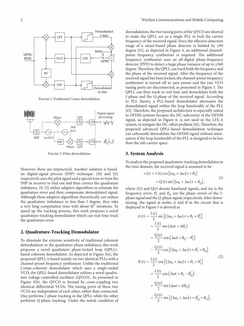
Most wireless communication systems use coherent demod-ulationmainly because the quality of coherent demodulationis much better than that of non-coherent demodulation[1] Traditional coherent demodulators are based on an RFquadrature demodulator But the RF coherent circuits areusually complex and power-hungry [2] To simplify thereceiverrsquos circuitry various phase-locked loop (PLL)-basedcoherent demodulators are adopted in wireless communi-cation systems The most well-known PLL-based coherentdemodulator has the Costas architecture [1 3ndash5] As depictedin Figure 1 this architecture uses a single PLL with twofeedback loops These two feedback loops demodulate thein-phase (I-phase) signal and quadrature-phase (Q-phase)signals respectively The demodulated signals are combinedand then tune the voltage-controlled oscillator (VCO) totrack the frequency of the carrier signal However both thetraditional quadrature demodulator and the Costas-coherentdemodulator face the problem of quadrature imbalance ofRF signal Quadrature imbalance of RF signal arises fromboth the quadrature transmitter and the quadrature receiverPrevious investigations have showed that a slight 25 degree
quadrature imbalance significantly degrades the demodu-lation quality of an OFDM signal which is extensivelyused in LTE-A systems [6 7] Although the conventionalCostas-coherent demodulator has two feedback loops fordemodulation the single-VCO design prevents tracking ofmore than one phase of a received signal
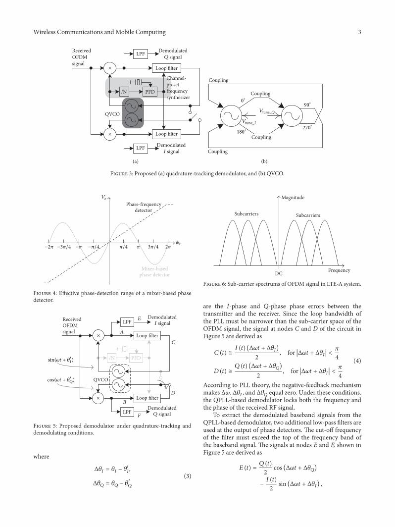
We [8] previously presented an alternative coherent polardemodulator without the quadrature imbalance problem ofreceiver As presented in Figure 2 the received signal isdivided into two paths One of these paths uses injection-locked oscillators (ILO) to extract the phase-modulatedcarrier signal and the phase information The extractedphase-modulated carrier is then mixed with the receivedsignal along another path The mixing cancels out the phaseinformation of these two input signals and then the envelopeinformation of the received signal is exported The basebandprocessor then recovers the baseband signal from both thedemodulated phase and the envelope information Howeverthe quadrature imbalance that is caused by the RF transmitterremains in the received signal
To overcome the quadrature imbalance problem someworks directly trimming or adjusting their RF circuits [9]
HindawiWireless Communications and Mobile ComputingVolume 2018 Article ID 8712414 8 pageshttpsdoiorg10115520188712414
2 Wireless Communications and Mobile Computing
QPSKBPSK +VCO
LPF
LPF
LPF
+1
minus1
minus
BPSK
QPSK
+
+1minus1
DemodulatedI-data
DemodulatedQ-data
90∘
Figure 1 Traditional Costas demodulator
AD
ADBPF
LPF
LPF
Mixer
Mixer
1st ILO
2ndILO
Digital signalprocessing
90∘
Figure 2 Polar demodulator
However these are impractical Another solution is based-on digital-signal process (DSP) technique [10] and [11]respectively uses the pilot signal and a special tone to train theDSP in receiver to find out and then correct the quadratureimbalance [9 12] utilize adaptive algorithms to estimate thequadrature error and then compensate demodulated signalAlthough these adaptive algorithms theoretically can reducethe quadrature imbalance to less than 1 degree they takea very long computation time with about 105 iterations Tospeed up the tracking process this work proposes a novelquadrature-tracking demodulator which can real-time trackthe quadrature error
2 Quadrature-Tracking Demodulator
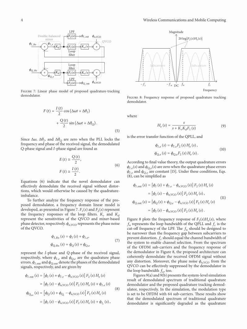
To eliminate the extreme sensitivity of traditional coherentdemodulation to the quadrature phase imbalance this workproposes a novel quadrature phase-locked loop (QPLL)-based coherent demodulator As depicted in Figure 3(a) theproposed QPLL is based mainly on two identical PLLs with achannel-preset frequency synthesizer Unlike the traditionalCostas-coherent demodulator which uses a single-endedVCO the QPLL-based demodulator utilizes a novel quadra-ture voltage-controlled oscillator (QVCO) As presented inFigure 3(b) the QVCO is formed by cross-coupling twoidentical differential VCOs The tuning ports of these twoVCOs are independent of each other rather than connectedOne performs I-phase tracking in the QPLL while the otherperforms Q-phase tracking Under the initial condition of
demodulation the two tuning ports of the QVCO are shortedto make the QPLL act as a single PLL to lock the carrierfrequency of the received signal Since the effective detectionrange of a mixer-based phase detector is limited by plusmn90degree [13] as depicted in Figure 4 an additional channel-preset frequency synthesizer is required The additionalfrequency synthesizer uses an all-digital phase-frequencydetector (PFD) to detect a large phase variance of up to plusmn360degreeTherefore theQPLL can track both the frequency andthe phase of the received signal After the frequency of thereceived signal has been locked the channel-preset frequencysynthesizer is turned off to save power and the two VCOtuning ports are disconnected as presented in Figure 5 TheQPLL can then track in real time and demodulate both theI-phase and the Q-phase of the received signal Accordingto PLL theory a PLL-based demodulator attenuates thedemodulated signal within the loop bandwidth of the PLL[13] Therefore the proposed architecture is especially suitedto OFDM systems because the DC-subcarrier of the OFDMsignal as depicted in Figure 6 is not used in the LTE-Asystem tomitigate the DC-offset problem [14]Therefore theproposed advanced QPLL-based demodulation techniquecan coherently demodulate the OFDM signal without atten-uation if the loop bandwidth of the PLL is designed to be lessthan the sub-carrier space
3 System Analysis
To analyze the proposed quadrature-tracking demodulator inthe time domain the received signal is assumed to be
119903 (119905) = 119868 (119905) cos [(1205960 + Δ120596) 119905 + 120579119868]+ 119876 (119905) sin [(1205960 + Δ120596) 119905 + 120579119876]
(1)
where 119868(119905) and 119876(119905) denote baseband signals and Δ120596 is thefrequency error 120579119868 and 120579119876 are the phase errors of the I-phase signal and theQ-phase signal respectively After down-mixing the signal at nodes A and B in the circuit that isdisplayed in Figure 5 is derived as
119860 (119905) = 119868 (119905)2 sin [(21205960 + Δ120596) 119905 + 120579119868 + 1205791015840119868]
+ 119868 (119905)2 sin (Δ120596119905 + Δ120579119868)
+ 119876 (119905)2 cos (Δ120596119905 + 120579119876 minus 1205791015840119868)
minus 119876 (119905)2 cos [(21205960 + Δ120596) t + 1205791015840119868 + 120579119876]
119861 (119905) = 119868 (119905)2 cos [(21205960 + Δ120596) 119905 + 120579119868 + 1205791015840119868]
+ 119868 (119905)2 cos (Δ120596119905 + 120579119868 minus 1205791015840119876)
+ 119876 (119905)2 sin (Δ120596119905 + Δ120579119876)
+ 119876 (119905)2 sin [(21205960 + Δ120596) 119905 + 1205791015840119876 + 120579119876]
(2)
Wireless Communications and Mobile Computing 3
Loop filter
ReceivedOFDMsignal
DemodulatedQ signalLPF
Loop filter
DemodulatedI signalLPF
N PFD
QVCO
Channel-presetfrequencysynthesizer
times
times
(a)
Coupling
Coupling
Coupling
Coupling
90∘
180∘270∘
0∘
VNOH_Q
VNOH_I
(b)
Figure 3 Proposed (a) quadrature-tracking demodulator and (b) QVCO
Mixer-basedphase detector
Phase-frequencydetector
Ve
eminus2 minus34 minus minus4 2344
Figure 4 Effective phase-detection range of a mixer-based phasedetector
Loop filter
DemodulatedI signalLPF
Loop filter
DemodulatedQ signalLPF
N PFD
QVCO
A
B
C
D
E
F
ReceivedOFDMsignal
MCH(t + I)
=IM(t + Q)
times
times
Figure 5 Proposed demodulator under quadrature-tracking anddemodulating conditions
where
Δ120579119868 = 120579119868 minus 1205791015840119868Δ120579119876 = 120579119876 minus 1205791015840119876
(3)
FrequencyDC
Magnitude
Subcarriers Subcarriers
Figure 6 Sub-carrier spectrums of OFDM signal in LTE-A system
are the I-phase and 119876-phase phase errors between thetransmitter and the receiver Since the loop bandwidth ofthe PLL must be narrower than the sub-carrier space of theOFDM signal the signal at nodes C and D of the circuit inFigure 5 are derived as
119862 (119905) cong 119868 (119905) (Δ120596119905 + Δ120579119868)2 for 1003816100381610038161003816Δ120596119905 + Δ1205791198681003816100381610038161003816 lt 120587
4119863 (119905) cong 119876 (119905) (Δ120596119905 + Δ120579119876)
2 for 1003816100381610038161003816Δ120596119905 + Δ1205791198681003816100381610038161003816 lt 1205874
(4)
According to PLL theory the negative-feedback mechanismmakes Δ120596 Δ120579119868 and Δ120579119876 equal zero Under these conditionsthe QPLL-based demodulator locks both the frequency andthe phase of the received RF signal
To extract the demodulated baseband signals from theQPLL-based demodulator two additional low-pass filters areused at the output of phase detectors The cut-off frequencyof the filter must exceed the top of the frequency band ofthe baseband signal The signals at nodes E and F shown inFigure 5 are derived as
119864 (119905) = 119876 (119905)2 cos (Δ120596119905 + Δ120579119876)
minus 119868 (119905)2 sin (Δ120596119905 + Δ120579119868)
4 Wireless Communications and Mobile Computing
QVCO
Loopfilter
LPF
Loopfilter
LPF
Double-balancedmixer
I_Rx
Q_Rx
Q_e
I_e
nVCO
nVCOQ_out
I_out
Kd
Kd
F1(s)
F2(s)
F1(s)
F2(s)
Ks
Ks
minus
+ +
+minus
+
Figure 7 Linear phase model of proposed quadrature-trackingdemodulator
119865 (119905) = 119868 (119905)2 cos (Δ120596119905 + Δ120579119868)
+ 119876 (119905)2 sin (Δ120596119905 + Δ120579119876) (5)
Since Δ120596 Δ120579119868 and Δ120579119876 are zero when the PLL locks thefrequency and phase of the received signal the demodulated119876-phase signal and 119868-phase signal are found as
119864 (119905) cong 119876 (119905)2
119865 (119905) cong 119868 (119905)2
(6)
Equations (6) indicate that the novel demodulator caneffectively demodulate the received signal without distor-tions which would otherwise be caused by the quadrature-imbalance
To further analyze the frequency response of the pro-posed demodulator a frequency domain linear model isdeveloped as presented in Figure 7 1198651(119904) and 1198652(119904) representthe frequency responses of the loop filters 119870V and 119870119889represent the sensitivities of the QVCO and mixer-basedphase detector respectively 120601119899VCO represents the phase noiseof the QVCO
120601119868 119877119909 (119904) = 120601119868 (119904) + 120601119868 119890120601119876 119877119909 (119904) = 120601119876 (119904) + 120601119876 119890
(7)
represent the I-phase and Q-phase of the received signalrespectively where 120601119868 119890 and 120601119876 119890 are the quadrature phaseerrors 120601119868 out and 120601119876 out denote the phases of the demodulatedsignals respectively and are given by
120601119868 out (119904) = [120601119868 (119904) + 120601119868 119890 minus 120601119899VCO (119904)] 1198652 (119904)119867119890 (119904)= [120601119868 (119904) minus 120601119899VCO (119904)] 1198652 (119904)119867119890 (119904) + 120601119868 119890 (119904)
120601119876out (119904) = [120601119876 (119904) + 120601119876119890 minus 120601119899VCO (119904)] 1198652 (119904)119867119890 (119904)= [120601119868 (119904) minus 120601119899VCO (119904)] 1198652 (119904)119867119890 (119904) + 120601119868
119890
(119904)
(8)
FrequencyDC
Magnitude
Subcarriers Subcarriers
minusfc minusfn fn fc
20 FIAF2(s)He(s)
Figure 8 Frequency response of proposed quadrature trackingdemodulator
where
119867119890 (119904) = 119904119904 + 119870V1198701198891198651 (119904) (9)
is the error transfer function of the QPLL and
120601119868 119890 (119904) = 120601119868 1198901198652 (119904)119867119890 (119904) 120601119876 119890 (119904) = 120601119876 1198901198652 (119904)119867119890 (119904)
(10)
According to final value theory the output quadrature errors120601119868 119890(119904) and 120601119876 119890(119904) are zero when the quadrature phase errors120601119868 119890 and 120601119876 119890 are constant [15] Under these conditions Eqs(8) can be simplified as
120601119868 out (119904) = [120601119868 (119904) + 120601119868 119890 minus 120601119899VCO (119904)] 1198652 (119904)119867119890 (119904)= [120601119868 (119904) minus 120601119899VCO (119904)] 1198652 (119904)119867119890 (119904)
120601119876 out (119904) = [120601119876 (119904) + 120601119876 119890 minus 120601119899VCO (119904)] 1198652 (119904)119867119890 (119904)= [120601119868 (119904) minus 120601119899VCO (119904)] 1198652 (119904)119867119890 (119904)
(11)
Figure 8 plots the frequency response of 1198652(119904)119867119890(119904) where119891119899 represents the loop bandwidth of the QPLL and 119891119888 is thecut-off frequency of the LPF The 119891119899 should be designed tobe narrower than the frequency gap between subcarriers toprevent distortion 119891119888 should equal the channel bandwidth ofthe system to enable channel selection From the spectrumof the OFDM sub-carriers and the frequency response ofthe demodulator in Figure 8 the proposed architecture cancoherently demodulate the received OFDM signal withoutany distortion Moreover the phase noise 120601119899VCO from theQVCO can be effectively suppressed by the demodulator inthe loop bandwidth 119891119899 too
Figures 9(a) and 9(b) presents the system-level simulationresult of demodulated spectrum of traditional quadraturedemodulator and the proposed quadrature tracking demod-ulator respectively In the simulation the modulation typeis set to be OFDM with 64 sub-carriers These results showthat the demodulated spectrum of traditional quadraturedemodulator is significantly degraded as the quadrature
Wireless Communications and Mobile Computing 5
0 10 20 30 40 50 60 70 80Subcarrier
02
04
06
08
1
12
14M
agni
tude
15 deg quadrature imbalance0 deg quadrature imbalance
(a)
0 10 20 30 40 50 60 70 80Subcarrier
0
02
04
06
08
1
12
14
Mag
nitu
de
15 deg quadrature imbalance0 deg quadrature imbalance
(b)
Figure 9 Demodulated spectrum of (a) traditional quadrature demodulator and (b) proposed quadrature tracking demodulator
Cou
plin
g po
rt_Q
minus
Cou
plin
g po
rt_Q
+C
oupl
ing
port
_I+
Cou
plin
g po
rt_I
minusOut
put_I+
Out
put_Iminus
Out
put_Q
+
Out
put_Q
+
Vtune_Q Vtune_I
V$$
(a) (b)
Figure 10 (a) Circuit and (b) CMOS chip of the QVCO
imbalance increasing from 0 degree to 15 degree Under thesame condition the demodulated spectrum of the proposedquadrature tracking demodulator shows a very slight decline
4 Experimental Results
The QVCO of the proposed demodulator was implementedusing TSMC 018120583m CMOS technology Figure 10(a) showsthe circuit design of the CMOS QVCO Generally a VCOwith internal NMOS cross-coupled pairs has a wider oper-ating range but a poorer phase noise performance than theone with internal PMOS cross-coupled pairs [18] Basedon consideration of both the phase noise performanceand operating range the internal complementary cross-coupled pair is used To realize quadrature outputs externalcross-coupling between two identical differential VCOs arerequired so four additional NMOS are designed to be parallel
to the original NMOS cross-coupled pair The outputs oftwo identical differential VCOs then cross-couple to eachother via the gates of the additional NMOSs These internaland external couplings of the VCOs force the four outputssignal quadrature each other Since the QPLLmust separatelytrack the I-phase and the Q-phase of the received signal theQVCO is designed to have two tuning ports as presentedin Figure 10(a) This architecture enables the quadrature ofthe QVCO to be slightly adjusted using the two independenttuning ports
Figure 10(b) displays the implemented CMOS QVCOchip The measured power consumption is less than 89mWThe operating range and output power of the CMOS QVCOare measured and presented in Figure 11(a) The CMOSQVCO can operate from 21 to 25 GHz with a mean out-put power of around 2 dBm which is sufficiently high todrive passive double-balance mixers for phase detectionThemeasured output power of the QVCO also exhibits very
6 Wireless Communications and Mobile Computing
10 >divlog
Mag
nitu
de (d
Bm)
(1)
minus500
minus150
minus250
minus350
minus450
minus550
minus650
minus750
minus850
Mkr1 2526 (T2563 >G
Center 21855(TRes BW 30-(T
VBW 50-(TSweep 100 GM (1001 JNM)
Ref 500 >G
Span 1000 (T
(a)
Phase noise (dBcHz)
minus130
minus110
minus90
minus70
minus50
Frequency offset
Top minus30 >=HzRF atten 5 >
10 E(T 100 E(T 1-(T 10-(T
(b)
Figure 11 Measured (a) operating range and output power and (b) phase noise of CMOS QVCO of demodulator
Table 1 Performance Comparison of 24GHz QVCOs
This work [16] [17]Process 018 120583m CMOS 018120583m CMOS 018 120583m CMOSSupply voltage (V) 14 06 18Power dissipation (mW) 55 144 148Frequency (GHz) 24 24 24Fractional bandwidth () 175 95 263Output power (dBm) 2 minus10 0Phase noise 1MHz (dBcHz) minus113 minus110simminus104 minus112Quadrature error (Degree) 69 264 5FoM 1MHz 1732 1664 1683
good flatness of better than 2 dB over the wide operatingrange Figure 11(b) plots the measured phase noise of theCMOS QVCO The phase noise is lower than minus113 dBcHzand minus137 dBcHz at 1MHz and 10MHz offset frequencyrespectively Table 1 shows the performance comparisonbetween 24GHz CMOS QVCOs where the figure of merit(FoM) is given by [19]
FoM = minusL (Δ120596) + 20 log( 1205960Δ120596) minus 10 log(119875diss1119898119882) (12)
The comparison shows that the implementedQVCOachievesa lowest phase noise and power consumption and conse-quently results in a better FoM over the other QVCOs
The proposed quadrature-tracking demodulator is imple-mented with the designed CMOS QVCO as presented inFigure 12 The channel-preset frequency synthesizer of thedemodulator is implemented using a consumer IC PE3336produced by Peregrine The phase detectors are the ZX05-C42 S+ model from Mini-Circuits The LPFs are the SLP-107+ model also from Mini-Circuits and have a 3 dBbandwidth of 14MHz The loop bandwidth of the QPLL isdesigned to be 10 kHz The received LTE-A signal of thereceiver is generated using a Keysight MXA vector signal
LPF
LPF
Splitter
Splitter
Loopfilters
Basebandoutput (I)
Basebandoutput (Q)
Testing board ofCMOS QVCO
Channel-presetfrequency
synthesizer
Phasedetector
Phasedetector
RFinput
Figure 12 Implemented quadrature-tracking de-modulator
Wireless Communications and Mobile Computing 7
imbalance imbalance15∘ quadrature0∘ quadrature
(a)
imbalance imbalance15∘ quadrature0∘ quadrature
(b)
Figure 13 Demodulated (a) I-phase and (b) Q-phase baseband waveforms when received LTE-A signal has a quadrature imbalance of 15∘
0 3 6 9 12 15Quadrature imbalance (degree)
10
15
20
25
30
SIN
AD
(dB)
Figure 14 Measured SINAD of the implemented quadrature-tracking demodulator
generator (VSG) with Keysight Signal StudioThe data rate ofthe LTE-A signal is set to be 18Mbps The sub-carrier spaceis set to 15625 kHz which greatly exceeds the 10 kHz loopbandwidth of the QPLL
Figures 13(a) and 13(b) presents the demodulated I-phase and Q-phase waveforms respectively To confirmthe quadrature-tracking performance of the implementeddemodulator the quadrature-imbalance of the LTE-A signalis manually adjusted in the signal studio As the quadrature-imbalance is increased from 0 degree to 15 degree both theI-phase and the Q-phase waveforms are degraded slightlyrevealing that the implemented quadrature-tracking demod-ulator can effectively demodulate the LTE-A signal even if thesignal has a 15∘ quadrature-imbalance
Figure 14 shows the measured signal to noise and distor-tion ratio (SINAD) degradation of the implemented demodu-lator as a function of quadrature imbalance Comparing withthe well-known signal to noise ratio (SNR) SINAD furtherconsiders the combining effect of both noise and distortion
Therefore the SINAD is usually used to evaluate performanceof RF receivers [20] SINAD is defined as
SINAD = 10 log 119875119878 + 119875119873 + 119875119863119875119873 + 119875119863= 10 log 119875DS
119875119873 + 119875119863 (dB) (13)
where 119875119878 119875DS 119875119873 and 119875119863 represents the power of the idealsignal distorted signal noise and distortion respectivelyThemeasured results show that the SINADslightly degrade asthe quadrature imbalance increase from0 degree to 15 degreeAs the quadrature imbalance is 15 degree the SINAD ofthe implemented quadrature-tracking demodulator is about18761 dB which is acceptable for most wireless communica-tion applications
5 Conclusion
In this work a novel quadrature tracking demodulatorfor LTE-A applications was implemented The 21sim25 GHzQPLL-based demodulator can effectively demodulate an18Mbps LTE-A signal with a quadrature-imbalance of upto 15 degrees This remarkable quadrature-tracking abilitymakes the novel demodulator well suited to LTE-A systemsor even more advanced communication systems
Conflicts of Interest
The authors declare that there is no conflicts of interestregarding the publication of this paper
Acknowledgments
The authors would like to thank the Ministry of Scienceand Technology (101-2221-E-327-029) for providing researchfunding The authors would also like to thank the NationalChip ImplementationCenter Hsinchu Taiwan for providingthe CMOS foundry service
8 Wireless Communications and Mobile Computing
References
[1] S Haykin and M Moher Communication Systems Wily USA5th edition 2009
[2] B Razavi and RF Microelectronics Prentice Hall Inc[3] G L Do ldquoAn ultra-fast carrier recovery versus traditional
synchronizersrdquo IEEE Transactions on Broadcasting vol 42 no1 pp 42ndash49 1996
[4] J P Costas ldquoSynchronous communicationsrdquo Proceedings of theIEEE vol 90 no 8 pp 1461ndash1466 2002
[5] S-J Huang Y-C Yeh H Wang P-N Chen and J Lee ldquoW-band BPSK and QPSK transceivers with Costas-loop carrierrecovery in 65-nm CMOS technologyrdquo IEEE Journal of Solid-State Circuits vol 46 no 12 pp 3033ndash3046 2011
[6] M Buchholz A Schuchert and R Hasholzner ldquoEffects of tunerIQ imbalance onmulticarrier-modulation systemsrdquo in Proceed-ings of the ICCDCS 2000 3rd IEEE International Conference onDevices Circuits and Systems pp T651ndashT656 March 2000
[7] M Rumney LTE and the Evolution to 4G Wireless Design andMeasurement Challenges JohnWiley amp Sons West Sussex UK2013
[8] C-T Chen C-H Hsiao T-S Horng K-C Peng and C-J LildquoCognitive polar receiver using two injection-locked oscillatorstagesrdquo IEEETransactions onMicrowaveTheory and Techniquesvol 59 no 12 pp 3484ndash3493 2011
[9] R Cherukuri and P T Balsara ldquoCode-aided adaptive decorrela-tor for IQ imbalance compensation in iterative receivers for flatfading channelsrdquo in Proceedings of theMilitary CommunicationsConference MILCOM 2007 USA October 2007
[10] L Giugno V Lottici and M Luise ldquoEfficient compensation ofIQ phase imbalance for digital receiversrdquo in Proceedings of the2005 IEEE International Conference on Communications ICC2005 pp 2462ndash2466 May 2005
[11] C-H Hsu C-F Wu and C-K Wang ldquoFPGA prototype forWLAN OFDM baseband with STPE of IQ mismatch selfcalibration algorithmrdquo inProceedings of the 1st IEEEAsian Solid-State Circuits Conference ASSCC 2005 pp 509ndash512 TaiwanNovember 2005
[12] G Vallant M Epp W Schlecker U Schneider L Anttilaand M Valkama ldquoAnalog IQ impairments in Zero-IF radarreceivers Analysis measurements and digital compensationrdquoin Proceedings of the IEEE International Instrumentation andMeasurement Technology Conference I2MTC 2012 pp 1703ndash1707 Austria May 2012
[13] K C PengModulated Frequency Synthesizers Design for Wide-band and High Efficiency Modulation VDM Verlag Germany2009
[14] M Rumney LTE and the Evolution to 4G Wireless - Design andMeasurement Challenges Second Edition John Wiley amp SonsWest Sussex UK 2008
[15] K-C Peng C-H Lee C-H Chen and T-S Horng ldquoEnhance-ment of frequency synthesizer operating range using a novelfrequency-offset technique for LTE-a and CR applicationsrdquoIEEE Transactions onMicrowaveTheory and Techniques vol 61no 3 pp 1215ndash1223 2013
[16] C T Lu H H Hsieh and L H Lu ldquoA low-power quadratureVCO and its application to a 06-V 24-GHz PLLrdquo IEEETransactions on Circuits and Systems I Regular Papers vol 57no 4 pp 793ndash802 2010
[17] S Shin K Lee and S M Kang ldquolow-power 24 GHz CMOSfrequency synthesizer with differentially controlledMOS varac-torsrdquo in Proceedings of the 2006 IEEE International Symposiumon Circuits and Systems pp 553ndash556 Island of Kos Greece
[18] K C Peng and C H Lee ldquoA 5 GHz CMOS quadrature VCOwith precise quadrature phaserdquo in Proceedings of the 2012Asia-Pacific Microwave Conference APMC 2012 pp 1211ndash1213Taiwan December 2012
[19] K C Peng and T S Horng ldquoOptimization of phase noise in a23 - 35 GHz voltage-controlled oscillator using the impedancelocusrdquo in Progress in Electromagnetics Research Symposium Digpp 913ndash917 2012
[20] Wikipedia contributors ldquoSINADrdquo Wikipedia The Free Ency-clopedia Available httpsenwikipediaorgwikiSINAD
International Journal of
AerospaceEngineeringHindawiwwwhindawicom Volume 2018
RoboticsJournal of
Hindawiwwwhindawicom Volume 2018
Hindawiwwwhindawicom Volume 2018
Active and Passive Electronic Components
VLSI Design
Hindawiwwwhindawicom Volume 2018
Hindawiwwwhindawicom Volume 2018
Shock and Vibration
Hindawiwwwhindawicom Volume 2018
Civil EngineeringAdvances in
Acoustics and VibrationAdvances in
Hindawiwwwhindawicom Volume 2018
Hindawiwwwhindawicom Volume 2018
Electrical and Computer Engineering
Journal of
Advances inOptoElectronics
Hindawiwwwhindawicom
Volume 2018
Hindawi Publishing Corporation httpwwwhindawicom Volume 2013Hindawiwwwhindawicom
The Scientific World Journal
Volume 2018
Control Scienceand Engineering
Journal of
Hindawiwwwhindawicom Volume 2018
Hindawiwwwhindawicom
Journal ofEngineeringVolume 2018
SensorsJournal of
Hindawiwwwhindawicom Volume 2018
International Journal of
RotatingMachinery
Hindawiwwwhindawicom Volume 2018
Modelling ampSimulationin EngineeringHindawiwwwhindawicom Volume 2018
Hindawiwwwhindawicom Volume 2018
Chemical EngineeringInternational Journal of Antennas and
Propagation
International Journal of
Hindawiwwwhindawicom Volume 2018
Hindawiwwwhindawicom Volume 2018
Navigation and Observation
International Journal of
Hindawi
wwwhindawicom Volume 2018
Advances in
Multimedia
Submit your manuscripts atwwwhindawicom
2 Wireless Communications and Mobile Computing
QPSKBPSK +VCO
LPF
LPF
LPF
+1
minus1
minus
BPSK
QPSK
+
+1minus1
DemodulatedI-data
DemodulatedQ-data
90∘
Figure 1 Traditional Costas demodulator
AD
ADBPF
LPF
LPF
Mixer
Mixer
1st ILO
2ndILO
Digital signalprocessing
90∘
Figure 2 Polar demodulator
However these are impractical Another solution is based-on digital-signal process (DSP) technique [10] and [11]respectively uses the pilot signal and a special tone to train theDSP in receiver to find out and then correct the quadratureimbalance [9 12] utilize adaptive algorithms to estimate thequadrature error and then compensate demodulated signalAlthough these adaptive algorithms theoretically can reducethe quadrature imbalance to less than 1 degree they takea very long computation time with about 105 iterations Tospeed up the tracking process this work proposes a novelquadrature-tracking demodulator which can real-time trackthe quadrature error
2 Quadrature-Tracking Demodulator
To eliminate the extreme sensitivity of traditional coherentdemodulation to the quadrature phase imbalance this workproposes a novel quadrature phase-locked loop (QPLL)-based coherent demodulator As depicted in Figure 3(a) theproposed QPLL is based mainly on two identical PLLs with achannel-preset frequency synthesizer Unlike the traditionalCostas-coherent demodulator which uses a single-endedVCO the QPLL-based demodulator utilizes a novel quadra-ture voltage-controlled oscillator (QVCO) As presented inFigure 3(b) the QVCO is formed by cross-coupling twoidentical differential VCOs The tuning ports of these twoVCOs are independent of each other rather than connectedOne performs I-phase tracking in the QPLL while the otherperforms Q-phase tracking Under the initial condition of
demodulation the two tuning ports of the QVCO are shortedto make the QPLL act as a single PLL to lock the carrierfrequency of the received signal Since the effective detectionrange of a mixer-based phase detector is limited by plusmn90degree [13] as depicted in Figure 4 an additional channel-preset frequency synthesizer is required The additionalfrequency synthesizer uses an all-digital phase-frequencydetector (PFD) to detect a large phase variance of up to plusmn360degreeTherefore theQPLL can track both the frequency andthe phase of the received signal After the frequency of thereceived signal has been locked the channel-preset frequencysynthesizer is turned off to save power and the two VCOtuning ports are disconnected as presented in Figure 5 TheQPLL can then track in real time and demodulate both theI-phase and the Q-phase of the received signal Accordingto PLL theory a PLL-based demodulator attenuates thedemodulated signal within the loop bandwidth of the PLL[13] Therefore the proposed architecture is especially suitedto OFDM systems because the DC-subcarrier of the OFDMsignal as depicted in Figure 6 is not used in the LTE-Asystem tomitigate the DC-offset problem [14]Therefore theproposed advanced QPLL-based demodulation techniquecan coherently demodulate the OFDM signal without atten-uation if the loop bandwidth of the PLL is designed to be lessthan the sub-carrier space
3 System Analysis
To analyze the proposed quadrature-tracking demodulator inthe time domain the received signal is assumed to be
119903 (119905) = 119868 (119905) cos [(1205960 + Δ120596) 119905 + 120579119868]+ 119876 (119905) sin [(1205960 + Δ120596) 119905 + 120579119876]
(1)
where 119868(119905) and 119876(119905) denote baseband signals and Δ120596 is thefrequency error 120579119868 and 120579119876 are the phase errors of the I-phase signal and theQ-phase signal respectively After down-mixing the signal at nodes A and B in the circuit that isdisplayed in Figure 5 is derived as
119860 (119905) = 119868 (119905)2 sin [(21205960 + Δ120596) 119905 + 120579119868 + 1205791015840119868]
+ 119868 (119905)2 sin (Δ120596119905 + Δ120579119868)
+ 119876 (119905)2 cos (Δ120596119905 + 120579119876 minus 1205791015840119868)
minus 119876 (119905)2 cos [(21205960 + Δ120596) t + 1205791015840119868 + 120579119876]
119861 (119905) = 119868 (119905)2 cos [(21205960 + Δ120596) 119905 + 120579119868 + 1205791015840119868]
+ 119868 (119905)2 cos (Δ120596119905 + 120579119868 minus 1205791015840119876)
+ 119876 (119905)2 sin (Δ120596119905 + Δ120579119876)
+ 119876 (119905)2 sin [(21205960 + Δ120596) 119905 + 1205791015840119876 + 120579119876]
(2)
Wireless Communications and Mobile Computing 3
Loop filter
ReceivedOFDMsignal
DemodulatedQ signalLPF
Loop filter
DemodulatedI signalLPF
N PFD
QVCO
Channel-presetfrequencysynthesizer
times
times
(a)
Coupling
Coupling
Coupling
Coupling
90∘
180∘270∘
0∘
VNOH_Q
VNOH_I
(b)
Figure 3 Proposed (a) quadrature-tracking demodulator and (b) QVCO
Mixer-basedphase detector
Phase-frequencydetector
Ve
eminus2 minus34 minus minus4 2344
Figure 4 Effective phase-detection range of a mixer-based phasedetector
Loop filter
DemodulatedI signalLPF
Loop filter
DemodulatedQ signalLPF
N PFD
QVCO
A
B
C
D
E
F
ReceivedOFDMsignal
MCH(t + I)
=IM(t + Q)
times
times
Figure 5 Proposed demodulator under quadrature-tracking anddemodulating conditions
where
Δ120579119868 = 120579119868 minus 1205791015840119868Δ120579119876 = 120579119876 minus 1205791015840119876
(3)
FrequencyDC
Magnitude
Subcarriers Subcarriers
Figure 6 Sub-carrier spectrums of OFDM signal in LTE-A system
are the I-phase and 119876-phase phase errors between thetransmitter and the receiver Since the loop bandwidth ofthe PLL must be narrower than the sub-carrier space of theOFDM signal the signal at nodes C and D of the circuit inFigure 5 are derived as
119862 (119905) cong 119868 (119905) (Δ120596119905 + Δ120579119868)2 for 1003816100381610038161003816Δ120596119905 + Δ1205791198681003816100381610038161003816 lt 120587
4119863 (119905) cong 119876 (119905) (Δ120596119905 + Δ120579119876)
2 for 1003816100381610038161003816Δ120596119905 + Δ1205791198681003816100381610038161003816 lt 1205874
(4)
According to PLL theory the negative-feedback mechanismmakes Δ120596 Δ120579119868 and Δ120579119876 equal zero Under these conditionsthe QPLL-based demodulator locks both the frequency andthe phase of the received RF signal
To extract the demodulated baseband signals from theQPLL-based demodulator two additional low-pass filters areused at the output of phase detectors The cut-off frequencyof the filter must exceed the top of the frequency band ofthe baseband signal The signals at nodes E and F shown inFigure 5 are derived as
119864 (119905) = 119876 (119905)2 cos (Δ120596119905 + Δ120579119876)
minus 119868 (119905)2 sin (Δ120596119905 + Δ120579119868)
4 Wireless Communications and Mobile Computing
QVCO
Loopfilter
LPF
Loopfilter
LPF
Double-balancedmixer
I_Rx
Q_Rx
Q_e
I_e
nVCO
nVCOQ_out
I_out
Kd
Kd
F1(s)
F2(s)
F1(s)
F2(s)
Ks
Ks
minus
+ +
+minus
+
Figure 7 Linear phase model of proposed quadrature-trackingdemodulator
119865 (119905) = 119868 (119905)2 cos (Δ120596119905 + Δ120579119868)
+ 119876 (119905)2 sin (Δ120596119905 + Δ120579119876) (5)
Since Δ120596 Δ120579119868 and Δ120579119876 are zero when the PLL locks thefrequency and phase of the received signal the demodulated119876-phase signal and 119868-phase signal are found as
119864 (119905) cong 119876 (119905)2
119865 (119905) cong 119868 (119905)2
(6)
Equations (6) indicate that the novel demodulator caneffectively demodulate the received signal without distor-tions which would otherwise be caused by the quadrature-imbalance
To further analyze the frequency response of the pro-posed demodulator a frequency domain linear model isdeveloped as presented in Figure 7 1198651(119904) and 1198652(119904) representthe frequency responses of the loop filters 119870V and 119870119889represent the sensitivities of the QVCO and mixer-basedphase detector respectively 120601119899VCO represents the phase noiseof the QVCO
120601119868 119877119909 (119904) = 120601119868 (119904) + 120601119868 119890120601119876 119877119909 (119904) = 120601119876 (119904) + 120601119876 119890
(7)
represent the I-phase and Q-phase of the received signalrespectively where 120601119868 119890 and 120601119876 119890 are the quadrature phaseerrors 120601119868 out and 120601119876 out denote the phases of the demodulatedsignals respectively and are given by
120601119868 out (119904) = [120601119868 (119904) + 120601119868 119890 minus 120601119899VCO (119904)] 1198652 (119904)119867119890 (119904)= [120601119868 (119904) minus 120601119899VCO (119904)] 1198652 (119904)119867119890 (119904) + 120601119868 119890 (119904)
120601119876out (119904) = [120601119876 (119904) + 120601119876119890 minus 120601119899VCO (119904)] 1198652 (119904)119867119890 (119904)= [120601119868 (119904) minus 120601119899VCO (119904)] 1198652 (119904)119867119890 (119904) + 120601119868
119890
(119904)
(8)
FrequencyDC
Magnitude
Subcarriers Subcarriers
minusfc minusfn fn fc
20 FIAF2(s)He(s)
Figure 8 Frequency response of proposed quadrature trackingdemodulator
where
119867119890 (119904) = 119904119904 + 119870V1198701198891198651 (119904) (9)
is the error transfer function of the QPLL and
120601119868 119890 (119904) = 120601119868 1198901198652 (119904)119867119890 (119904) 120601119876 119890 (119904) = 120601119876 1198901198652 (119904)119867119890 (119904)
(10)
According to final value theory the output quadrature errors120601119868 119890(119904) and 120601119876 119890(119904) are zero when the quadrature phase errors120601119868 119890 and 120601119876 119890 are constant [15] Under these conditions Eqs(8) can be simplified as
120601119868 out (119904) = [120601119868 (119904) + 120601119868 119890 minus 120601119899VCO (119904)] 1198652 (119904)119867119890 (119904)= [120601119868 (119904) minus 120601119899VCO (119904)] 1198652 (119904)119867119890 (119904)
120601119876 out (119904) = [120601119876 (119904) + 120601119876 119890 minus 120601119899VCO (119904)] 1198652 (119904)119867119890 (119904)= [120601119868 (119904) minus 120601119899VCO (119904)] 1198652 (119904)119867119890 (119904)
(11)
Figure 8 plots the frequency response of 1198652(119904)119867119890(119904) where119891119899 represents the loop bandwidth of the QPLL and 119891119888 is thecut-off frequency of the LPF The 119891119899 should be designed tobe narrower than the frequency gap between subcarriers toprevent distortion 119891119888 should equal the channel bandwidth ofthe system to enable channel selection From the spectrumof the OFDM sub-carriers and the frequency response ofthe demodulator in Figure 8 the proposed architecture cancoherently demodulate the received OFDM signal withoutany distortion Moreover the phase noise 120601119899VCO from theQVCO can be effectively suppressed by the demodulator inthe loop bandwidth 119891119899 too
Figures 9(a) and 9(b) presents the system-level simulationresult of demodulated spectrum of traditional quadraturedemodulator and the proposed quadrature tracking demod-ulator respectively In the simulation the modulation typeis set to be OFDM with 64 sub-carriers These results showthat the demodulated spectrum of traditional quadraturedemodulator is significantly degraded as the quadrature
Wireless Communications and Mobile Computing 5
0 10 20 30 40 50 60 70 80Subcarrier
02
04
06
08
1
12
14M
agni
tude
15 deg quadrature imbalance0 deg quadrature imbalance
(a)
0 10 20 30 40 50 60 70 80Subcarrier
0
02
04
06
08
1
12
14
Mag
nitu
de
15 deg quadrature imbalance0 deg quadrature imbalance
(b)
Figure 9 Demodulated spectrum of (a) traditional quadrature demodulator and (b) proposed quadrature tracking demodulator
Cou
plin
g po
rt_Q
minus
Cou
plin
g po
rt_Q
+C
oupl
ing
port
_I+
Cou
plin
g po
rt_I
minusOut
put_I+
Out
put_Iminus
Out
put_Q
+
Out
put_Q
+
Vtune_Q Vtune_I
V$$
(a) (b)
Figure 10 (a) Circuit and (b) CMOS chip of the QVCO
imbalance increasing from 0 degree to 15 degree Under thesame condition the demodulated spectrum of the proposedquadrature tracking demodulator shows a very slight decline
4 Experimental Results
The QVCO of the proposed demodulator was implementedusing TSMC 018120583m CMOS technology Figure 10(a) showsthe circuit design of the CMOS QVCO Generally a VCOwith internal NMOS cross-coupled pairs has a wider oper-ating range but a poorer phase noise performance than theone with internal PMOS cross-coupled pairs [18] Basedon consideration of both the phase noise performanceand operating range the internal complementary cross-coupled pair is used To realize quadrature outputs externalcross-coupling between two identical differential VCOs arerequired so four additional NMOS are designed to be parallel
to the original NMOS cross-coupled pair The outputs oftwo identical differential VCOs then cross-couple to eachother via the gates of the additional NMOSs These internaland external couplings of the VCOs force the four outputssignal quadrature each other Since the QPLLmust separatelytrack the I-phase and the Q-phase of the received signal theQVCO is designed to have two tuning ports as presentedin Figure 10(a) This architecture enables the quadrature ofthe QVCO to be slightly adjusted using the two independenttuning ports
Figure 10(b) displays the implemented CMOS QVCOchip The measured power consumption is less than 89mWThe operating range and output power of the CMOS QVCOare measured and presented in Figure 11(a) The CMOSQVCO can operate from 21 to 25 GHz with a mean out-put power of around 2 dBm which is sufficiently high todrive passive double-balance mixers for phase detectionThemeasured output power of the QVCO also exhibits very
6 Wireless Communications and Mobile Computing
10 >divlog
Mag
nitu
de (d
Bm)
(1)
minus500
minus150
minus250
minus350
minus450
minus550
minus650
minus750
minus850
Mkr1 2526 (T2563 >G
Center 21855(TRes BW 30-(T
VBW 50-(TSweep 100 GM (1001 JNM)
Ref 500 >G
Span 1000 (T
(a)
Phase noise (dBcHz)
minus130
minus110
minus90
minus70
minus50
Frequency offset
Top minus30 >=HzRF atten 5 >
10 E(T 100 E(T 1-(T 10-(T
(b)
Figure 11 Measured (a) operating range and output power and (b) phase noise of CMOS QVCO of demodulator
Table 1 Performance Comparison of 24GHz QVCOs
This work [16] [17]Process 018 120583m CMOS 018120583m CMOS 018 120583m CMOSSupply voltage (V) 14 06 18Power dissipation (mW) 55 144 148Frequency (GHz) 24 24 24Fractional bandwidth () 175 95 263Output power (dBm) 2 minus10 0Phase noise 1MHz (dBcHz) minus113 minus110simminus104 minus112Quadrature error (Degree) 69 264 5FoM 1MHz 1732 1664 1683
good flatness of better than 2 dB over the wide operatingrange Figure 11(b) plots the measured phase noise of theCMOS QVCO The phase noise is lower than minus113 dBcHzand minus137 dBcHz at 1MHz and 10MHz offset frequencyrespectively Table 1 shows the performance comparisonbetween 24GHz CMOS QVCOs where the figure of merit(FoM) is given by [19]
FoM = minusL (Δ120596) + 20 log( 1205960Δ120596) minus 10 log(119875diss1119898119882) (12)
The comparison shows that the implementedQVCOachievesa lowest phase noise and power consumption and conse-quently results in a better FoM over the other QVCOs
The proposed quadrature-tracking demodulator is imple-mented with the designed CMOS QVCO as presented inFigure 12 The channel-preset frequency synthesizer of thedemodulator is implemented using a consumer IC PE3336produced by Peregrine The phase detectors are the ZX05-C42 S+ model from Mini-Circuits The LPFs are the SLP-107+ model also from Mini-Circuits and have a 3 dBbandwidth of 14MHz The loop bandwidth of the QPLL isdesigned to be 10 kHz The received LTE-A signal of thereceiver is generated using a Keysight MXA vector signal
LPF
LPF
Splitter
Splitter
Loopfilters
Basebandoutput (I)
Basebandoutput (Q)
Testing board ofCMOS QVCO
Channel-presetfrequency
synthesizer
Phasedetector
Phasedetector
RFinput
Figure 12 Implemented quadrature-tracking de-modulator
Wireless Communications and Mobile Computing 7
imbalance imbalance15∘ quadrature0∘ quadrature
(a)
imbalance imbalance15∘ quadrature0∘ quadrature
(b)
Figure 13 Demodulated (a) I-phase and (b) Q-phase baseband waveforms when received LTE-A signal has a quadrature imbalance of 15∘
0 3 6 9 12 15Quadrature imbalance (degree)
10
15
20
25
30
SIN
AD
(dB)
Figure 14 Measured SINAD of the implemented quadrature-tracking demodulator
generator (VSG) with Keysight Signal StudioThe data rate ofthe LTE-A signal is set to be 18Mbps The sub-carrier spaceis set to 15625 kHz which greatly exceeds the 10 kHz loopbandwidth of the QPLL
Figures 13(a) and 13(b) presents the demodulated I-phase and Q-phase waveforms respectively To confirmthe quadrature-tracking performance of the implementeddemodulator the quadrature-imbalance of the LTE-A signalis manually adjusted in the signal studio As the quadrature-imbalance is increased from 0 degree to 15 degree both theI-phase and the Q-phase waveforms are degraded slightlyrevealing that the implemented quadrature-tracking demod-ulator can effectively demodulate the LTE-A signal even if thesignal has a 15∘ quadrature-imbalance
Figure 14 shows the measured signal to noise and distor-tion ratio (SINAD) degradation of the implemented demodu-lator as a function of quadrature imbalance Comparing withthe well-known signal to noise ratio (SNR) SINAD furtherconsiders the combining effect of both noise and distortion
Therefore the SINAD is usually used to evaluate performanceof RF receivers [20] SINAD is defined as
SINAD = 10 log 119875119878 + 119875119873 + 119875119863119875119873 + 119875119863= 10 log 119875DS
119875119873 + 119875119863 (dB) (13)
where 119875119878 119875DS 119875119873 and 119875119863 represents the power of the idealsignal distorted signal noise and distortion respectivelyThemeasured results show that the SINADslightly degrade asthe quadrature imbalance increase from0 degree to 15 degreeAs the quadrature imbalance is 15 degree the SINAD ofthe implemented quadrature-tracking demodulator is about18761 dB which is acceptable for most wireless communica-tion applications
5 Conclusion
In this work a novel quadrature tracking demodulatorfor LTE-A applications was implemented The 21sim25 GHzQPLL-based demodulator can effectively demodulate an18Mbps LTE-A signal with a quadrature-imbalance of upto 15 degrees This remarkable quadrature-tracking abilitymakes the novel demodulator well suited to LTE-A systemsor even more advanced communication systems
Conflicts of Interest
The authors declare that there is no conflicts of interestregarding the publication of this paper
Acknowledgments
The authors would like to thank the Ministry of Scienceand Technology (101-2221-E-327-029) for providing researchfunding The authors would also like to thank the NationalChip ImplementationCenter Hsinchu Taiwan for providingthe CMOS foundry service
8 Wireless Communications and Mobile Computing
References
[1] S Haykin and M Moher Communication Systems Wily USA5th edition 2009
[2] B Razavi and RF Microelectronics Prentice Hall Inc[3] G L Do ldquoAn ultra-fast carrier recovery versus traditional
synchronizersrdquo IEEE Transactions on Broadcasting vol 42 no1 pp 42ndash49 1996
[4] J P Costas ldquoSynchronous communicationsrdquo Proceedings of theIEEE vol 90 no 8 pp 1461ndash1466 2002
[5] S-J Huang Y-C Yeh H Wang P-N Chen and J Lee ldquoW-band BPSK and QPSK transceivers with Costas-loop carrierrecovery in 65-nm CMOS technologyrdquo IEEE Journal of Solid-State Circuits vol 46 no 12 pp 3033ndash3046 2011
[6] M Buchholz A Schuchert and R Hasholzner ldquoEffects of tunerIQ imbalance onmulticarrier-modulation systemsrdquo in Proceed-ings of the ICCDCS 2000 3rd IEEE International Conference onDevices Circuits and Systems pp T651ndashT656 March 2000
[7] M Rumney LTE and the Evolution to 4G Wireless Design andMeasurement Challenges JohnWiley amp Sons West Sussex UK2013
[8] C-T Chen C-H Hsiao T-S Horng K-C Peng and C-J LildquoCognitive polar receiver using two injection-locked oscillatorstagesrdquo IEEETransactions onMicrowaveTheory and Techniquesvol 59 no 12 pp 3484ndash3493 2011
[9] R Cherukuri and P T Balsara ldquoCode-aided adaptive decorrela-tor for IQ imbalance compensation in iterative receivers for flatfading channelsrdquo in Proceedings of theMilitary CommunicationsConference MILCOM 2007 USA October 2007
[10] L Giugno V Lottici and M Luise ldquoEfficient compensation ofIQ phase imbalance for digital receiversrdquo in Proceedings of the2005 IEEE International Conference on Communications ICC2005 pp 2462ndash2466 May 2005
[11] C-H Hsu C-F Wu and C-K Wang ldquoFPGA prototype forWLAN OFDM baseband with STPE of IQ mismatch selfcalibration algorithmrdquo inProceedings of the 1st IEEEAsian Solid-State Circuits Conference ASSCC 2005 pp 509ndash512 TaiwanNovember 2005
[12] G Vallant M Epp W Schlecker U Schneider L Anttilaand M Valkama ldquoAnalog IQ impairments in Zero-IF radarreceivers Analysis measurements and digital compensationrdquoin Proceedings of the IEEE International Instrumentation andMeasurement Technology Conference I2MTC 2012 pp 1703ndash1707 Austria May 2012
[13] K C PengModulated Frequency Synthesizers Design for Wide-band and High Efficiency Modulation VDM Verlag Germany2009
[14] M Rumney LTE and the Evolution to 4G Wireless - Design andMeasurement Challenges Second Edition John Wiley amp SonsWest Sussex UK 2008
[15] K-C Peng C-H Lee C-H Chen and T-S Horng ldquoEnhance-ment of frequency synthesizer operating range using a novelfrequency-offset technique for LTE-a and CR applicationsrdquoIEEE Transactions onMicrowaveTheory and Techniques vol 61no 3 pp 1215ndash1223 2013
[16] C T Lu H H Hsieh and L H Lu ldquoA low-power quadratureVCO and its application to a 06-V 24-GHz PLLrdquo IEEETransactions on Circuits and Systems I Regular Papers vol 57no 4 pp 793ndash802 2010
[17] S Shin K Lee and S M Kang ldquolow-power 24 GHz CMOSfrequency synthesizer with differentially controlledMOS varac-torsrdquo in Proceedings of the 2006 IEEE International Symposiumon Circuits and Systems pp 553ndash556 Island of Kos Greece
[18] K C Peng and C H Lee ldquoA 5 GHz CMOS quadrature VCOwith precise quadrature phaserdquo in Proceedings of the 2012Asia-Pacific Microwave Conference APMC 2012 pp 1211ndash1213Taiwan December 2012
[19] K C Peng and T S Horng ldquoOptimization of phase noise in a23 - 35 GHz voltage-controlled oscillator using the impedancelocusrdquo in Progress in Electromagnetics Research Symposium Digpp 913ndash917 2012
[20] Wikipedia contributors ldquoSINADrdquo Wikipedia The Free Ency-clopedia Available httpsenwikipediaorgwikiSINAD
International Journal of
AerospaceEngineeringHindawiwwwhindawicom Volume 2018
RoboticsJournal of
Hindawiwwwhindawicom Volume 2018
Hindawiwwwhindawicom Volume 2018
Active and Passive Electronic Components
VLSI Design
Hindawiwwwhindawicom Volume 2018
Hindawiwwwhindawicom Volume 2018
Shock and Vibration
Hindawiwwwhindawicom Volume 2018
Civil EngineeringAdvances in
Acoustics and VibrationAdvances in
Hindawiwwwhindawicom Volume 2018
Hindawiwwwhindawicom Volume 2018
Electrical and Computer Engineering
Journal of
Advances inOptoElectronics
Hindawiwwwhindawicom
Volume 2018
Hindawi Publishing Corporation httpwwwhindawicom Volume 2013Hindawiwwwhindawicom
The Scientific World Journal
Volume 2018
Control Scienceand Engineering
Journal of
Hindawiwwwhindawicom Volume 2018
Hindawiwwwhindawicom
Journal ofEngineeringVolume 2018
SensorsJournal of
Hindawiwwwhindawicom Volume 2018
International Journal of
RotatingMachinery
Hindawiwwwhindawicom Volume 2018
Modelling ampSimulationin EngineeringHindawiwwwhindawicom Volume 2018
Hindawiwwwhindawicom Volume 2018
Chemical EngineeringInternational Journal of Antennas and
Propagation
International Journal of
Hindawiwwwhindawicom Volume 2018
Hindawiwwwhindawicom Volume 2018
Navigation and Observation
International Journal of
Hindawi
wwwhindawicom Volume 2018
Advances in
Multimedia
Submit your manuscripts atwwwhindawicom
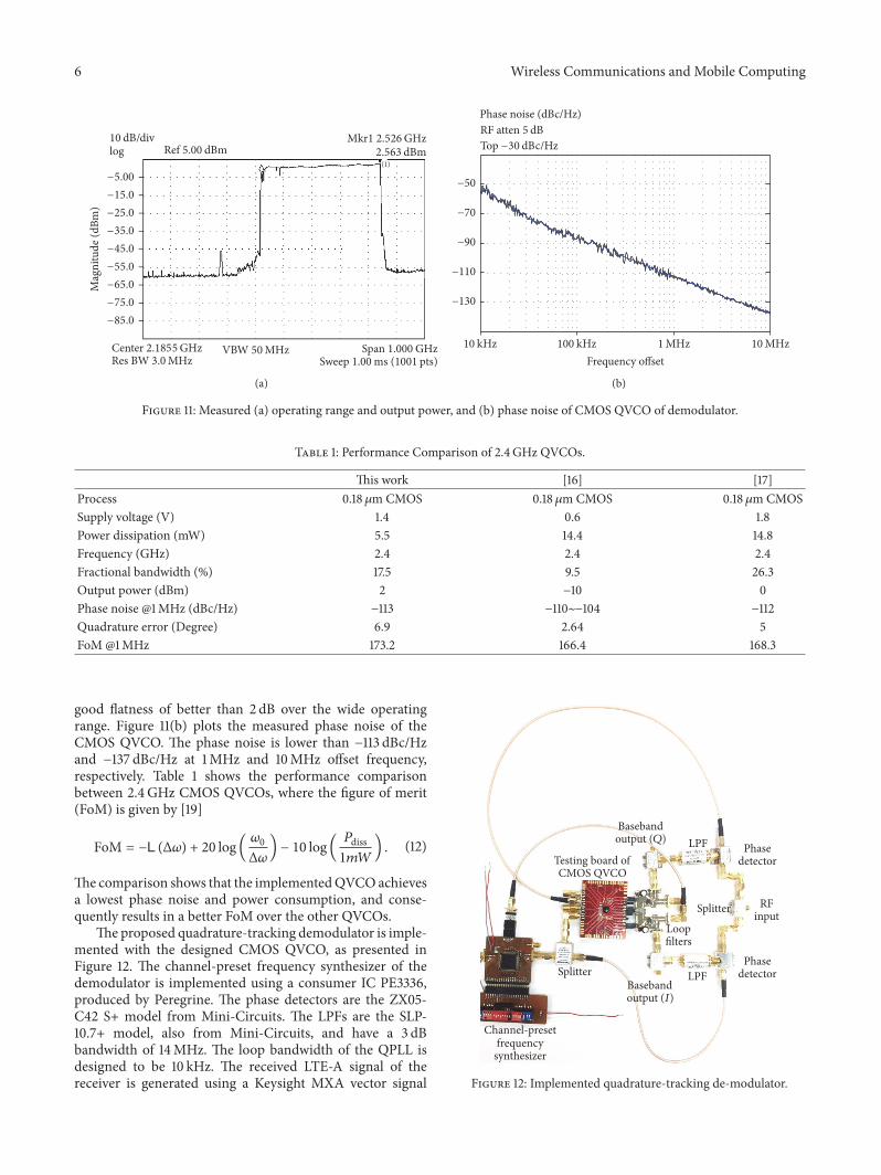
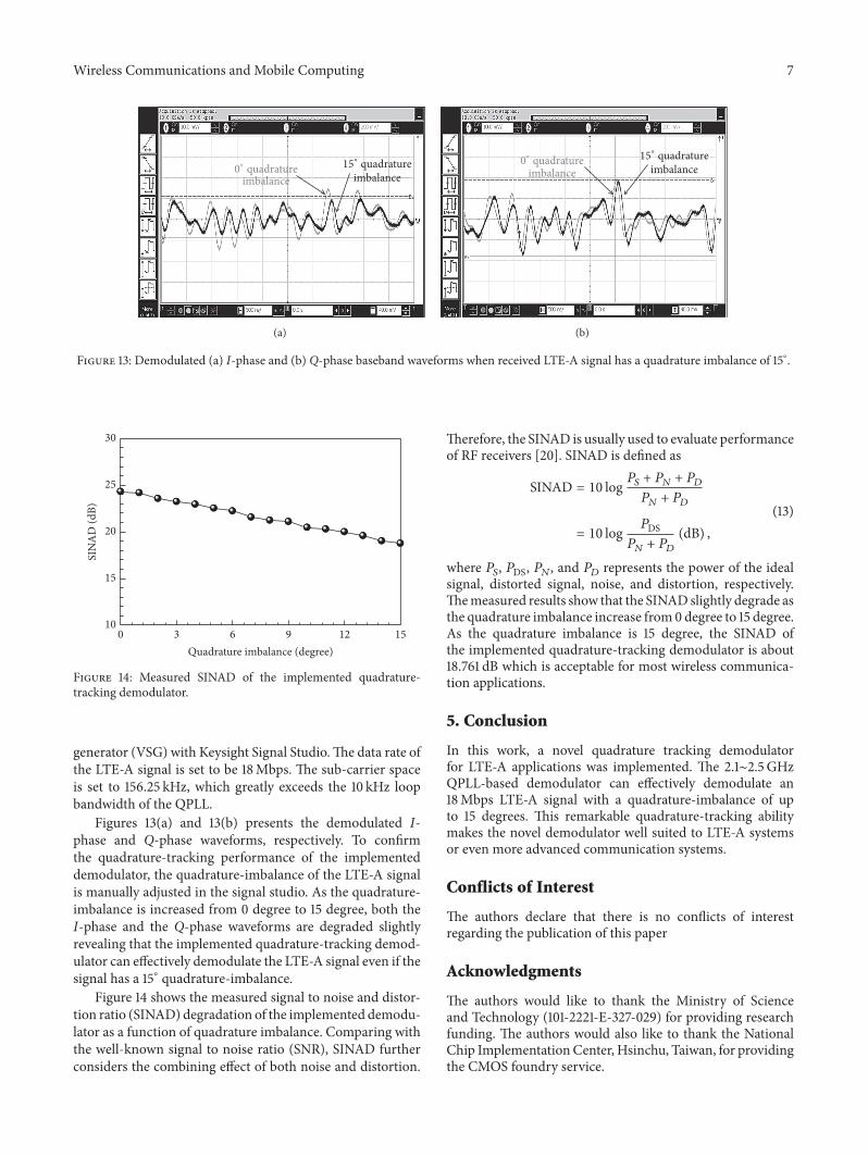

International Journal of
AerospaceEngineeringHindawiwwwhindawicom Volume 2018
RoboticsJournal of
Hindawiwwwhindawicom Volume 2018
Hindawiwwwhindawicom Volume 2018
Active and Passive Electronic Components
VLSI Design
Hindawiwwwhindawicom Volume 2018
Hindawiwwwhindawicom Volume 2018
Shock and Vibration
Hindawiwwwhindawicom Volume 2018
Civil EngineeringAdvances in
Acoustics and VibrationAdvances in
Hindawiwwwhindawicom Volume 2018
Hindawiwwwhindawicom Volume 2018
Electrical and Computer Engineering
Journal of
Advances inOptoElectronics
Hindawiwwwhindawicom
Volume 2018
Hindawi Publishing Corporation httpwwwhindawicom Volume 2013Hindawiwwwhindawicom
The Scientific World Journal
Volume 2018
Control Scienceand Engineering
Journal of
Hindawiwwwhindawicom Volume 2018
Hindawiwwwhindawicom
Journal ofEngineeringVolume 2018
SensorsJournal of
Hindawiwwwhindawicom Volume 2018
International Journal of
RotatingMachinery
Hindawiwwwhindawicom Volume 2018
Modelling ampSimulationin EngineeringHindawiwwwhindawicom Volume 2018
Hindawiwwwhindawicom Volume 2018
Chemical EngineeringInternational Journal of Antennas and
Propagation
International Journal of
Hindawiwwwhindawicom Volume 2018
Hindawiwwwhindawicom Volume 2018
Navigation and Observation
International Journal of
Hindawi
wwwhindawicom Volume 2018
Advances in
Multimedia
Submit your manuscripts atwwwhindawicom