A DISSERTATION - TDL
171
PLASMA-ENHANCED CHEMICAL VAPOR DEPOSITION OF LOW DIELECTRIC CONSTANT MATERIALS by BASHAR IBRAHIM LAHLOUH, B.S., M.S. A DISSERTATION IN PHYSICS Submitted to the Graduate Faculty of Texas Tech University in Partial Fulfillment of the Requirements for the Degree of DOCTOR OF PHILOSOPHY Approved Chairperson of the Comniittee —t—I M— T-r- r V C— Accepted Dean of the Graduate School May, 2003
Transcript of A DISSERTATION - TDL
PLASMA-ENHANCED CHEMICAL VAPOR DEPOSITION
OF LOW DIELECTRIC CONSTANT MATERIALS
by
BASHAR IBRAHIM LAHLOUH, B.S., M.S.
A DISSERTATION
IN
PHYSICS
Submitted to the Graduate Faculty of Texas Tech University in
Partial Fulfillment of the Requirements for
the Degree of
DOCTOR OF PHILOSOPHY
Approved
Chairperson of the Comniittee —t—I M—
T- r -
r V C—
Accepted
Dean of the Graduate School
May, 2003

ACKNOWLEDGMENTS
I would like to extend my sincere thanks to Dr. Shubhra Gangopadhyay for her
guidance and encouragement during my work. Her devotion for science was the guiding
light for me through out my PhD. research. If it was not for her persistent "high-
pressure," I would have never reached this point. Dr. Shubhra, thank you.
I would like also to thank my committee members. Dr. Sindee Simon, Dr. Henryk
Temkin, and Dr. Mark Holtz, for their time and their help. Their scientific careers are the
best examples for me to follow.
Special thanks also goes to Dr. Sindee Simon group for the great work on SSCO2
experiments. I do extend my thanks to Juan Sun, Dinghai Huang, and P. Doshi for their
help on the SCCO2 projects.
I would like also to extend the most sincere appreciation for my low k group
members. This work would have been impossible without their contributions. Thank you
all my friends, Jorge Lubguban, T. Rajagopalan, Nivedeta Biswas, N. Metha, Harlan R.
Harris, and X. Wang.
My warmest thanks go to my wife Montaha for her great support and her great
patience. I could have never made it all the way here without the momentum and the
energy she put into my life. Also, I would like to thank the joy of my life, my son Maher.
He always forced me to crack that smile regardless of how hard life is.
I also would like to thank my parents, the spirit of my life. Nothing would have
been possible without their overwhelming love and support. I owe them my life, and what
ever I do, I will never be able thank them enough.
Finally, there are many other names I need to thank here, for all those who are not
mentioned here: thank you very much.
11

TABLE OF CONTENTS
AKNOWLEDGEMENTS ii
ABSTRACT
LIST OF TABLES v
vii
LIST OF FIGURES viii
CHAPTER
I. INTRODUCTION
1.1 Motivation and Introduction 1
1.2 Spin-Coated Low-k Films 5
1.3 Chemical Vapor Deposited (CVD) Low-k Films 10
1.4 Present Research 20
II. THEORY
2.1 Molecular Polarizability and Clausius-Mossotti Equation 23
2.2 Maxwell's Equations and Frequency-Dependent
Polarizabilities 26
2.3 Plasma and Chemical Vapor Deposition 28
2.3.1 Plasma 28
2.3.2 Chemical Vapor Deposition (CVD) 33
2.4 Supercritical Carbon Dioxide (SCCO2) Processes 42
2.5 Optical and Electrical Characterization 51
2.5.1 Fourier Transform Infrared Spectroscopy (FTIR) 51
2.5.2 Ultraviolet-Visible (UV-Vis) Absorption 64
2.5.3 Dielectric Constant and Electrical Measurements 67
2.5.4 Porosity Calculation 68
2.5.5 Prism Coupler 69
111

III. NANOPOROUS TRIPLE-PHASE a-SiC:H/SiO/C:H
LOW-k FILMS 71
3.1 The Experiment 71
3.2 Annealing Treatments of a-SiC:H/SiO/C:H Films 73
3.3 SCC02/Annealing Treatment of the a-SiC:H/SiO/C:H Films 85
IV. LOW-k ORGANOSILICATE FILMS 87
4.1 TVTMCTS Organosilicate Films 88
4.2 SCC02 Treatment of Fluorinated Organosilicate Fihns 101
4.3 SCC02 Porogen Extraction 111
4.4 Hybrid Organosilicate Films Prepared by CVD 119
V. SUPERCRITICAL CARBON DIOXIDE TREATMENTS OF PLASMA-DAMAGED LOW-k FILMS 121
5.1 SCC02/HMDS0 Treatment 121
5.2 SCC02/HMDS Treatment 134
5.3 Contact Angle Measurements of SCCO2/HMDS Treated MSQ Films 145
VI. CONCLUSION 147
6.1 Triple Phase a-SiC:H/SiO/C:H Fihns 147
6.2 Organosilicate and Fluorinated Organosilicate Fihns Deposited from TVTMCTS 148
6.3 SCCO2 Treatment of Plasma-Damaged Porous
Low-k Films 149
6.4 Future Work 149
REFERENCES 150
IV

ABSTRACT
Plasma-enhanced chemical vapor deposition (PECVD) and supercritical carbon
dioxide (SCCO2) were used to create nanoporous low dielectric constant (low-k) films.
A material with low dielectric constant (~2) is needed to reduce the crosstalk noise and
the dissipated power in these circuits. Amorphous SiC:H/SiO/C:H films were deposited
using PECVD. Aimealing treatments and supercritical carbon dioxide (SCCO2)
freatments were used to selectively remove or reduce the concentration of one phase. The
removal of the methyl (CHn) group associated with the C:H phase introduced
nanoporosity in these films and low-k values of 2.1 were obtained. The effects of
different deposition and treatment parameters on the structural and electrical properties of
the films were studied.
In another project, a new source, tetravinyltetramethylcyclotetrasiloxane
(TVTMCTS), was used as a precursor for depositing organosilicate low-k films. This
source has a ring structure, if preserved, introduces free volume that helps to lower the k
value of the film. An organosilicate/fluorocarbon composite film was also deposited, and
SCCO2 was used to selectively remove the fluorocarbon phase in an attempt to introduce
porosity to these films. Dielectric constant values as low as 2.48 were obtained for these
films. Finally, SCCO2 was used to cure plasma damaged nanoporoiu-s low-k film. Plasma
ashing of low-k films removes the methyl group and replace it with the silanol group.
This increases the dielectric constant of the material. SCCO2 was used as a carrier for
hexamethyldisiloxane (HMDSO) and hexamethyldisilazane (HMDS) to reverse the
plasma-damage; SCCO2 carries HMDSO or HMDS to every point in the film and
HMDSO or HMDS reacts with the silanol group and replaces it with the methyl group.
The dielectric constant reduced from 3.71 for the plasma-damaged films to 2.3 for the
treated films. This k value is similar to the undamaged film. Annealing the treated films
at 400°C indicates that the SCCO2/HMDSO treatment is thermally unstable. The
SCCO2/HMDSO treated film lost almost all the added methyl groups after the high

temperature annealing. The SCCO2/HMDS treatment was thermally stable with 400°C
annealing and there was no methyl group loss.
VI
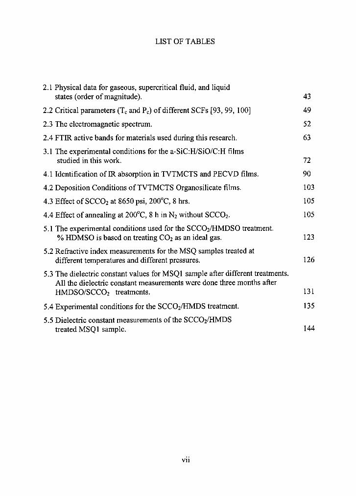
LIST OF TABLES
2.1 Physical data for gaseous, supercritical fluid, and liquid
states (order of magnitude). 43
2.2 Critical parameters (Tc and Pc) of different SCFs [93, 99, 100] 49
2.3 The electromagnetic spectrum. 52
2.4 FTIR active bands for materials used during this research. 63
3.1 The experimental conditions for the a-SiC:H/SiO/C:H films
studied in this work. 72
4.1 Identification of IR absorption in TVTMCTS and PECVD films. 90
4.2 Deposition Conditions of TVTMCTS Organosilicate films. 103
4.3 Effect of SCCO2 at 8650 psi, 200°C, 8 hrs. 105
4.4 Effect of annealing at 200''C, 8 h in N2 without SCCO2. 105
5.1 The experimental conditions used for the SCCO2/HMDSO treatment. % HDMSO is based on treating CO2 as an ideal gas. 123
5.2 Refractive index measurements for the MSQ samples treated at different temperatures and different pressures. 126
5.3 The dielectric constant values for MSQl sample after different treatments. All the dielectric constant measurements were done three months after HMDSO/SCCO2 treatments. 131
5.4 Experimental conditions for the SCCO2/HMDS treatment. 135
5.5 Dielectric constant measurements of the SCCO2/HMDS treated MSQl sample. 144
vu

LIST OF FIGURES
1.1 A representation of the different components of the molecular polarizability. (Adopted from reference [12].) 3
1.2 Dielectric constant components response as a function of the
frequency of the applied electric field. (Adapted from reference [9].) 4
1.3 The chemical structure of MSQ before and after curing. 9
2.1 A simple DC glow discharge reactor. 29
2.2 An illustration of the dark spaces in the DC plasma body. 30
2.3 DC voltage as a function of position in RF discharge. 32
2.4 The PECVD system used for this research. 34
2.5 Illustration of the steps confroUing the reaction kinetics in a
CVD process. (Adapted from reference [80].) 37
2.6 Laminar flow pattern in a circular tube (Adapted from [81].) 38
2.7 Growth process model. The gas flow is perpendicular to the
plane of the paper 40
2.8 A general phase diagram of the different states of the material [95, 96]. 43
2.9 Solubility (mole fraction) of naphthalene in CO2 as a function. of temperature at different pressures. (Adapted from [93].) 45
2.10 SolubiHty (mole fraction) of naphthalene in CO2 as a function of density at different temperatures. (Adapted from [93].) 45
2.11 Solubility (mole fraction) of naphthalene ethylene as a function of pressure at different temperatures. (Adapted from [93].) 46
2.12 Diffusivity of CO2 as a function of temperature at different pressures. (Adapted from [93].) 47
2.13 Viscosity of CO2 at different temperature and pressiu-es.
(Adapted from [93].) 48
2.14 Schematic diagram of the supercritical system used in this research. 50
2.15 The schematics of the Maddox lab SCCO2 system. 51
2.16 Comparison between the Absorption and the Transmission spectra of an a-SiC sample. 53
viu

2.17 A slice of thickness {dx) of an absorbing material. 54
2.18 Fundamental molecular vibrations possible for a molecule. The response of the molecules to IR radiations will be in the form of one of these vibrations. 57
2.19 Transitions between the vibrational states. Energy levels are not to scale. 61
2.20 Change in the density of states near the band gap. 65
2.21 Band-tailing effect as seen in the density of states diagram. 66
2.22 Band diagram representing a direct fransition between the valence and conduction bands. 67
2.23 The setup for CV or IV electrical measurements. For capacitance measurements on heavily doped substrate on of the probing terminals is placed on the subsfrate. 68
2.24 The schematics of a prism coupler and an example of one measurement using this technique. 70
3.1 FTIR specfra of (a) as-deposited and (b) 450°C annealed a-SiC:H/ SiO/ C:H film. 75
3.2 Changes in the SiO concentration after the different annealing temperatures. 75
3.3 The Gaussian fitting of the CHn band for the as-deposited film. 76
3.4 The Gaussian fitting of the CHn band for the film # 3 after 450°C annealing. 77
3.5 Effect of gas flow ratio (R) on the concentration (arb. units) of SiO, SiCH3, SiHn, and CHn bonds. 79
3.6 Effect of gas flow ratio (R) on the dielectric constant of the as-deposited films. 80
3.7 Effect of RF power on the concentration (arb. units) of CHn, SiHn, and SiCH3 bonds. 81
3.8 Effect of RF power on the dielectric constant of the as-deposited fihns. 82
3.9 Changes in thickness of film #3 after the different annealing temperatures. 82
3.10 Effect of the different annealing temperatures on the concenfration
of CHn, OH, SiHn, SiCH3, and C=0 bonds in the films. 83
3.11 Effect of the different annealing temperatures on the refractive index. 84
3.12 Effect of the different annealing temperatures on the dielectric constant (k) of films 1 and 3. 85
IX

4.1 The structure of TVTMCTS precursor. 88
4.2 IR specfra of the liquid TVTMCTS and the PECVD film. A magnified comparison of the CHn (n = 2,3) band is shown on the upper right. 91
4.3 Behavior of the dielectric constant and concentration of Si-CH3 bonds as a function of deposition pressure. 92
4.4 Behavior of the dielectric constant and concentration of Si-CH3 bonds as a function of deposition temperature. 93
4.5 Gaussian curve fit of the Si-0 band for two films deposited at 0.6 Torr and 1.75 Torr. Each spectrum is fitted with three Gaussian ciu-ves. 95
4.6 Concentration of Si-0 (ring) bonds as a function of deposition pressure and temperatiu-e . 96
4.7 Comparison of the CHn (n = 2,3) absorption bands for films deposited at 23 and 400°C. 97
4.8 Absorption intensity of CHn (n =2,3) bonds as a fimction of
deposition pressure and temperature. 98
4.9 UV-visible spectra of TVTMCTS and PECVD fihn. 99
4.10 Optical band gap of PECVD films as a function of deposition pressure and temperature. 99
4.11 Variation of the dielectric constant of the PECVD film with respect to annealing temperature. 100
4.12 Variation of the Si-CH3 and Si-0 bonds of the PECVD
fihns with respect to aimealing temperature. 101
4.13 FTIR specfra of as-deposited and SCCO2 a-C:F film. 106
4.14 Comparison of as-deposited organosihcate and composite film specfra. 108
4.15 Close-up of the normalized Si-0 band of the organosihcate film and the fluorinated organosilicate film. 109
4.16 Changes in the absorpfion intensity of 950-1250 band after
SCCO2 pressurization. 110
4.17 FTIR spectra of MSSQ, PPG, and MSSQ/PPG films. 113
4.18 The effect of SCCO2 treatment on the CHn in the MSSQ/PPG hybrid fihn. Thermal extraction at 430°C of PPG is also shown. 114
4.19 Comparison of the static, pulsed SCCO2, and thermal decomposition treatments. 115

4.20 Effective dielectric constant as a function of the volume fraction for MSSQ films. Maxwell-Gamett equation was used to calculate k(q) for the case ki= 3.1 and k2=l. 117
4.21 Effective dielectric constant as a fimction of the volume fraction for MSSQ films. Bruggemarm equation was used to calculate k{V) for the case ki= 3.1 and k2=l. 118
4.22 FTIR spectra of the organosilicate film, PMMA film, hybrid organosilicate/PMMA film, and the hybrid film after H2 plasma freatment. 120
5.1 The structure of the HMDSO molecule. 122
5.2 The FTIR specfra of the samples in the as-received state. MSQl and the MSQ2 are the plasma-treated films, while MSQ3 is the film without any treatment. The insets show the CH3 and OH bands of these films. 125
5.3 IR absorbance specfra for (a) As-received MSQl and (b) MSQl pressurized at 9000psi and 150°C in 10% HMDSO for 30 minutes. 128
5.4 IR absorption spectra of CH groups after pressurization at different temperatures. 128
5.5 IR absorption spectra of OH group after pressurization at different temperatures. 129
5.6 Effect of pressurization and temperature on CH concentration in MSQ samples. 129
5.7 Effect of pressurization and temperature on OH concentration in MSQ samples. 130
5.8 FTIR absorbance spectra of the (a) as-received, (b) SCCO2/HMDSO treated and (c) SCCO2/HMDSO treated + annealed MSQl sample. 132
5.9 Concentration of CH bonds in (a) as-received (b) SCCO2/HMDSO treated and (c) freated + 400°C annealed samples. 133
5.10 Concentration of OH bonds in (a) as-received (b) SCCO2/HMDSO freated and (c) treated + 400°C annealed MSQl samples. 133
5.11 Increased absorption of moisture with time after treatment in
case of SCCO2/ HMDSO freated MSQl sample. 134
5.12 The structure of the HMDS molecule. 135
5.13 The increase in the CH3 concentration as a function of SCCO2/HMDS treatment temperature. 137
5.14 Shift in the peak position and peak width after HMDS treatment of MSQl samples at different temperatiu-es. 138
XI

5.15 Effect of SCCO2/HMDS treatment temperature on the concentration of CH3 bonds. 138
5.16 A plot of the absorption intensity in the OH region of the spectrum for MSQl samples treated at different temperatures. 139
5.17 Dependence of the concentration of OH bonds removed on the treatment temperature. 140
5.18 The steric hindrance of the added Methyl group. 141
5.19 FTIR absorbance spectra of (a) plasma damaged MSQl, (b) HMDS/SCCO2 freated MSQl at 150°C for 30 minutes and (c) Treated MSQl sample annealed at 400°C for one hoiu-. Insets show the CH and OH regions of the specfra. 143
5.20 Contact angle measurements as a function of the treatment time for the new nanoporous MSQ samples. 146
xn
CHAPTER I
INTRODUCTION
1.1 Motivations and Introduction
High performance devices set very stringent requirements on the size and density
of the new generation of ultra large-scale integrated circuits (ULSI). The continuous
shrinkage in device dimensions requires the development of new technologies and
materials. According to the International Technology Roadmap for Semiconductor
(ITRS) [1], the minimiun feature size will be at 65 nm by the year 2007. Developing the
proper low dielectric (low-k) insulator for this generation of devices is crucial to
eliminate the problems pertinent to high density wiring in these circuits. Due to the high
on-chip signal frequency, serious problems like cross talk, dissipated power and
resistance-capacitance (RC) time delay starts to have a huge impact on the performance
of these devices [2-5].
To improve interconnect performance in the new device generations; Al
metallization is being replaced with the only available lower resistivity (R) Cu [6]. As the
intercormect density continues to increase, the need to reduce the RC delay also increase.
Since there is no other material available to replace Cu at this point, replacing the low k
insulator is the only choice left to reduce the RC delay in the new generations of ULSI
devices.
The dielectric constant (k) is a material property that measures the material
polarization under the influence of an external electric field. When a dielectric material is
placed in an external electric field, the charges in this material redistribute with respect to
each other. This characteristic of the material is known as the material polarizability. The
material polarizability can be attributed to the different components of the material and it
can be classified as electronic, ionic or dipolar (configurational) polarizability [7-12].
Figure 1.1 shows the difference between the different components of the molecular
polarizabilities.

The electronic polarizability arises from the fact that atoms consist of a heavy
positive nucleus surrounded by a lighter negatively charged electronic shell. When an
external electric field is applied, the negatively charged electrons are displaced from the
heavy nucleus creating a non-zero dipole moment. Due to the lighter mass of the
elecfrons, they can follow the change in the applied electric field more efficiently than the
heavier nucleus. Due to this fact, the effect of electronic polarizability on the dielectric
constant becomes the dominant polarizability component only at frequencies of the order
of the UV and visible frequencies (>10''' Hz)[12].
When the atoms covalently bond to create molecules, they share their valence
elecfrons and the elecfronic density around each atom can be different according to its
electronegativity. The electronegativity of an atom can simply be defined as its tendency
to attract the bonding electrons. This difference in the electronic density leaves one part
of the molecule with excess negative charge, and a partially ionic (polar) molecule is
created. The molecules can also bond ionically, when the difference in the
elecfronegativity is large between two atoms, one atom loses electron(s) to the other
atom, and they create an ionic bond. Due to the size of the atoms involved in the ionic
and the partially ionic (polar covalent) bonding, this kind of polarizability will be
dominant in the IR range (10 Hz) or lower. Also, at these frequencies the massive nuclei
begin to follow the change in the field, which changes the polarizability of the dielectric
material. Another part of this component of the polarizability is the induced dipole
moments; at this frequency range the bonds start to stretch due this induced dipole. This
component of polarizability is called the ionic (atomic) polarizability.
If the configuration of the bonded atoms is not symmetric and the charge
distribution is not symmetric, a permanent dipole moment is created. When an external
electric field is applied, the permanent dipoles try to align themselves accordingly. This
component of polarizability is called dipolar. Due to the large size of the molecules
involved in the dipolar component, the frequency range where this kind of polarizability
becomes prominent is in the microwave frequency range (10 Hz).

At the current device operating frequencies, lO^Hz, the three components of the
molecular polarizabihty contribute to the dielectric constant of the dielectric insulator [7].
Figure 1.2 is adapted from reference [12], and it illustrates the different active
components of the molecular polarizability at the different frequencies of the
elecfromagnetic spectrum.
Electronic O Ionic (atomic) ,^^ ,^^ +cr
O—o O o
Dipolar ^
E-field off E-field on
Figiu-e 1.1 A representation of the different components of the molecular polarizability. (Adapted from reference [12].)
Choosing the atoms involved in creating the dielectric material can reduce the
molecular polarizabilty. The choice of the precursor with atoms that have the proper
elecfronegativity and then bonding them in the proper configuration can bring the
molecular polarizability to low values. Another method that can be used to reduce the
molecular polarizability is to reduce the density of the fihns. Lower density
configurations of the dielectric material correspond to lower density of the components
that contribute to the molecular polarizability. Accordingly, lower density films tend to
show lower dielectric constant values.
One of the most atfractive methods to reduce the dielectric constant of the
material is to introduce free volume in the form of porosity. Since the dielectric constant
of air is 1, then introducing porosity to the low-k film reduces its effective dielectric
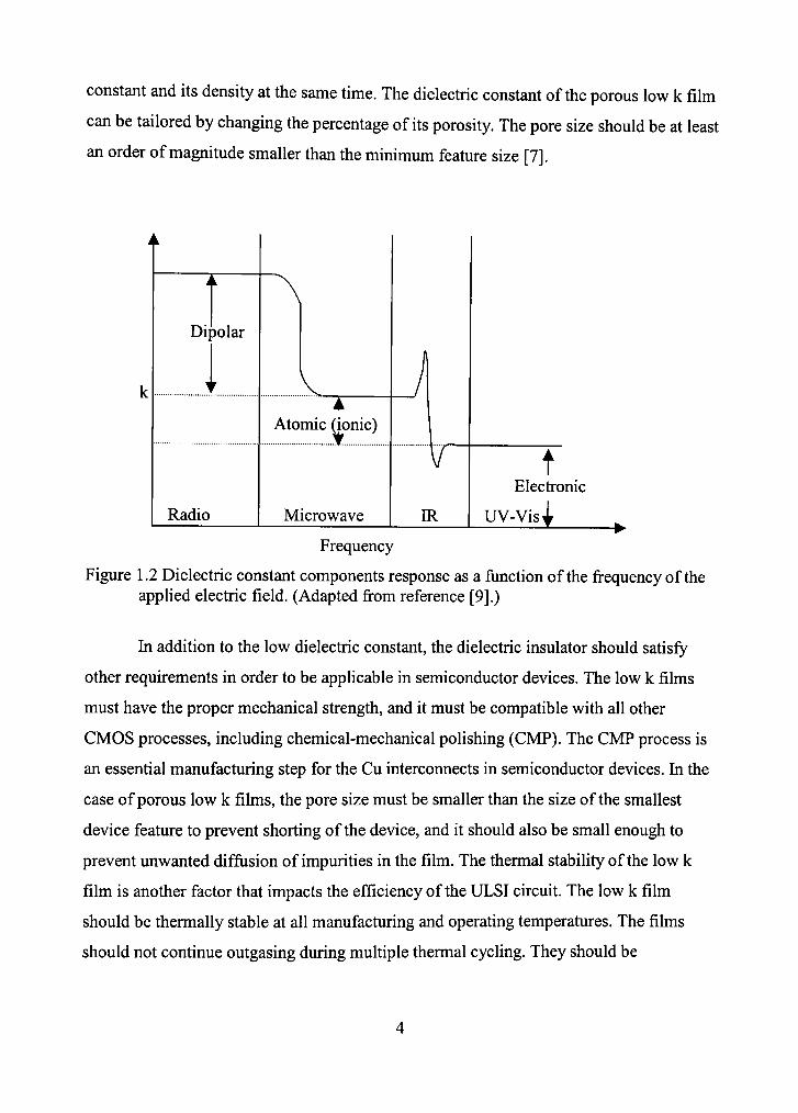
constant and its density at the same time. The dielectric constant of the porous low k film
can be tailored by changing the percentage of its porosity. The pore size should be at least
an order of magnitude smaller than the minimum feature size [7].
Dipolar
Radio
Atomic (ionic)
k
Microwave
\r IR
t Elecfronic
UV-Vis I
Frequency
Figure 1.2 Dielectric constant components response as a fimction of the frequency of the applied electric field. (Adapted from reference [9].)
In addition to the low dielectric constant, the dielectric insulator should satisfy
other requirements in order to be applicable in semiconductor devices. The low k fihns
must have the proper mechanical strength, and it must be compatible with all other
CMOS processes, including chemical-mechanical polishing (CMP). The CMP process is
an essential manufacturing step for the Cu interconnects in semiconductor devices. In the
case of porous low k films, the pore size must be smaller than the size of the smallest
device feature to prevent shorting of the device, and it should also be small enough to
prevent unwanted diffusion of impurities in the film. The thermal stability of the low k
film is another factor that impacts the efficiency of the ULSI circuit. The low k film
should be thermally stable at all manufacturing and operating temperatures. The films
should not continue outgasing during muhiple thermal cycling. They should be

compatible in the coefficient of thermal expansion of the substrate to prevent cracking or
delamination. The thermal conductivity of the low k films has to be high enough to allow
the films to dissipate the heat generated during operation [13-15], which can be a serious
challenge for low-density films.
Low dielectric constant films can be manufactured using different ways. The most
popular contenders for making low dielectric constant films are chemical vapor
deposition (CVD) and spin coating. Each method has its advantages and disadvantages,
but both methods are used widely to produce low k films with different properties.
Different configurations of the deposition systems and a large number of materials were
tested and studied as a potential precursor to deposit the proper low k dielectric. Material
polarizability and its dielectric constant were found to greatly depend on the chosen
precursor and how it is being deposited using the different techniques and systems. The
number of variables that needs to be tuned to get the proper film is different from one
deposition technique to another and from one deposition system to another. In the
following two sections an overview of some of the work done on low k films will be
offered.
1.2 Spin-Coated Low-k Films
To prepare spin-coated low-k films, a solution that contains the required material
is prepared. This solution can be a single or multi-component solution depending on the
planned scheme of the experiment. The solution is then spin coated to the required
thickness. The thickness of the spun film is a function of the solution viscosity, spin
speed and spin time. The films then can be exposed to several curing steps depending on
the nature of the used solution. Thermal or optical (UV) curing can be used depending on
the crosslinking and bonding mechanism of the spun film. Creating nanoporosity in these
films can by done by a foaming process or it can be created by loading a sacrificial
component into the main material, and then removing this sacrificial component after
curing the main structure. An immense amount of work was done on spin-on low k films;
here we will review some of the work that has been done on low k materials using this
technique.
Moon-Ho Jo and H. Park et al. [16-18] spun-coated Si02 aerogel and xerogel
films. The difference between aerogels and xerogels is how they are dried [14,19-22].
Aerogels are dried using supercritical drying; this reduces the capillary forces of the
solvent and facilitates its removal. The absence of capillary forces during the drying
process of aerogels helps to prevent the collapse of the structure. In the xerogels case, the
wetting angle between the network and the solvent is reduced by modifying the Si02
network siu-face. Both processes aim to remove the solvent without collapsing or
cracking the film. The films were prepared from Si02 sol prepared by a two-step
acid/base process with tetraethoxysilane (TEOS) as a precursor. Isopropyl alcohol (IPA)
or ethanol was used as solvents. To minimize solvent extraction, the films were spun
imder solvent atmosphere. In one set of experiments, the films were supercritically dried.
Those aerogel films prepared with IPA as a solvent showed dielectric constant values as
low as 2.0 after 450°C aimealing. The Fourier Transform Infrared (FTIR) spectrum of
these films reveals that the films consist mainly of an Si02peak at 1060-1080 cm'', C-H
peaks in the range 2936-2978 cm"' and a broad Si-OH peak in the range 3200-3800 cm"'.
Aimealing the films at 450°C removed both the C-H and the Si-OH bonds and reduced
the dielectric constant to 2.0. Thermal treatment caused a 10% decrease in the thickness.
The average pore size measured for these films was in the range of 10-30 nm. A second
set of experiment was conducted by this group with aerogel films dried in a solvent
ambient and then subjected to a series of chemical treatments to modify their chemical
structure. The reported dielectric constant values for these films were in the range of 2.2-
2.8 [17]. For the xerogel films with ethanol used as a solvent, similar dielectric constant
values were reported for films with porosity of-73%) and pore size in the range of 30-40
nm [18]. With this pore size and porosity, these films cannot be used as a proper low k
insulator. The group also studied the effect of O2 plasma treatment on the Si02 aerogel
films [23], and found that the O2 plasma treatment eliminates the surface chemical
groups. The FTIR spectra of the films before and after O2 plasma treatment show that the
C-H species were removed and OH was incorporated.
Yun Liu et al. [24] used TEOS mixed with water under NH4OH catalyst (base
catalyst) and polyvinyl alcohol (PVA) as a solvent to prepare a low k film. The spun film
temperature was then raised to 400°C for 2 min. using rapid thermal annealing (RTA),
then the film was allowed to cool down and then reheated slowly to 550°C and left at that
temperature for 30 min. The FTIR spectrum shows similar peaks to the films reported
before. Annealing the films at 350°C decreased the C-H content. Further annealing at
550°C removed both the C-H and the OH from the film. A 50%) porosity and 3.5 [xm
thickness was reported for these films.
B. P. Gorman et al. [25] prepared a fluorinated low-k xerogel derived from
triethoxyfluorosilane (TEES). The TEES was mixed with a solvent and a catalyst to
prepare these films. In addition the Si-O peaks; the FTIR spectrum indicates the existence
of the Si-F band in the range of 880-1000 cm"'. The fluorine existence distorts the Si-O
ring and increase tetrahedral silica, which decreases the film polarizability and thus its
dielectric constant. A dielectric constant value of 2.1 was reported for the as processed
film, and a 2.3 value was measured for the film annealed at 450°C. This increase in the
dielectric constant was explained by the loss of fluorine upon annealing. In confrast to
xerogel films made from other precursor, these films have different microstructure, and
they show thicker links, which improves their mechanical sfrength.
A. Nakashima et al. [26] developed a low-k spin on glass (SOG) material made
from inorganic hydrogen silsesquioxane (HSQ). HSQ films can suffer from low curing
controllability, hydrogen degassing, difficult film formation, moisture absorption and low
mechanical strength. This group developed a hydrophobic low k porous SOG by the
controlled drying and gelation of the precursor. Oligomers formed by hydrolysis of
alokoxysilanes and silanes are used as a binder in the SOG, and it can improve the metal
adhesion properties by controlling the organic/inorganic composition. They also foimd
that the films could be made hydrophobic by using binder that contains Si-H groups.
Dielectric constant values as low as 2.5 were achieved by infroducing more Si-H as a
binder in the SOG film, and good mechanical strength with 5nm cracking resistance was
also reported for these films.
Qi Pan et al. [27] used thermal and ultraviolet-irradiation methods to make SOG
films from a novel polysilsesquioxane. They used y5-chloroethyl-silsesquioxane
(BCESSQ) as a precursor. The advantage of the new precursor is the controlled release of
the reaction products and the retarded formation of the quaternary bonded silicon atom. A
two-step formation process is adapted to make these films. The films can first be heated
to about 225°C to partially convert the material to organically modified silica fihn, then
the films can be heated to 400°C to remove the chlorine from the film. The second route
that can be taken is that the films can be irradiated using ultraviolet (UV) radiation, it was
found that this irradiation process can change BCESSQ to organically modified silica
film rapidly. Detailed Rutherford backscattering spectroscopy (RBS) and forward recoil
specfrometry (FRES) were performed on the UV irradiated and thermally cured films. As
a result of these measurements, it was found that the decrease in the chlorine
concenfration during the irradiation process is quicker than the decrease in the
concentration of the hydrogen and the carbon compared to the thermal process. The
density of UV irradiated film was also less than that of the thermally treated film.
Suzhu Yu et al. [28] used a muhi-step sol-gel process to manufacture nanoporous
silica fihns. In this approach, sol A, prepared from TEOS in ethanol with HCl as a
catalyst, and Sol B, prepared from methyltriethoxysilane (MTES) in ethanol with NH4OH
catalyst were the precursors to make these films. A solution made from the two sols was
prepared and coated. The films were then baked and soaked into a hexamethyldisilazane
(HMDS) /toluene solution to convert the siu-face silanol groups into methyl groups. A
crack-free film was formed, and for films treated at high temperature in an air/N2
atmosphere, dielectric constant values as low as 1.89 were possible with 56%) porosity.
Shu Yang et al. [29] used a triblock polymer, poly(ethylene oxide-6-propylene
oxide-^7-ethylene oxide) (PEO-6-PPO-6-PEO), as a template in
poly(methylselsisquioxane) (MSQ) matrix. The PEO-6-PPO-6-PEO was dissolved in n-
butanol and then mixed with MSQ. The spun film was first cured in air at 120°C for 30
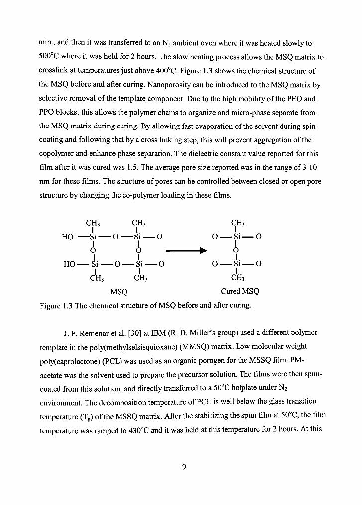
min., and then it was transferred to an N2 ambient oven where it was heated slowly to
500°C where it was held for 2 hours. The slow heating process allows the MSQ matrix to
crosslink at temperatures just above 400°C. Figure 1.3 shows the chemical structure of
the MSQ before and after curing. Nanoporosity can be introduced to the MSQ matrix by
selective removal of the template component. Due to the high mobility of the PEO and
PPO blocks, this allows the polymer chains to organize and micro-phase separate from
the MSQ matrix dining curing. By allowing fast evaporation of the solvent during spin
coating and following that by a cross linking step, this will prevent aggregation of the
copolymer and enhance phase separation. The dielectric constant value reported for this
film after it was cured was 1.5. The average pore size reported was in the range of 3-10
nm for these films. The structure of pores can be controlled between closed or open pore
structure by changing the co-polymer loading in these films.
CH3 CH3 CH3 I I I
HO Si O Si O O Si O I I I
O O ^ O I I I
HO Si O Si O O Si O I I I
CH3 CH3 CH3
MSQ Cured MSQ
Figure 1.3 The chemical structure of MSQ before and after curing.
J. F. Remenar et al. [30] at IBM (R. D. Miller's group) used a different polymer
template in the poly(methylselsisquioxane) (MMSQ) matrix. Low molecular weight
poly(caprolactone) (PCL) was used as an organic porogen for the MSSQ fihn. PM-
acetate was the solvent used to prepare the precursor solution. The films were then spun-
coated from this solution, and directly transferred to a 50°C hotplate under N2
environment. The decomposition temperature of PCL is well below the glass transition
temperature (Tg) of the MSSQ matiix. After the stabilizing the spun film at 50°C, the film
temperature was ramped to 430°C and it was held at this temperature for 2 hours. At this
temperature the PCL thermally decompose leaving MSSQ matrix intact. By controlling
the PCL loading the porosity can be controlled. The nature of the pore structure, open or
closed, can also be controlled by the PCL loading.
T. C. Chang et al. [31] studied enhancing the thermal stability of hydrogen
silsesquioxane (HSQ) films up to temperatures as high as 500°C. Fluorine ion
implantation at 70 keV was performed on HSQ films before and after 400°C curing. The
implantation process densified the imcured film. This caused an increase in the refractive
index and the dielectric constant, and the thickness decreased due to this densification.
The FTER spectnun of the ion implanted film shows reduction in the Si-H and the caged
structured Si-0 in the HSQ film. The thermal stability of the films, which was first cured
at 400°C and then ion implanted using fluorine ions is improved. Thermal stability of
these films comes at the cost of the dielectric constant, which was increased from 2.8 to
3.2 due to fihn densification.
C. Y. Wang et al. [32, 33] studied the thermal properties and thermal curing of
MSSQ films. They studied the effects of thermal treatment on the structure of the films
and their crosslinking. High temperature FTIR studies on this film show that the
evaporation of the solvent starts at room temperature and is almost complete at 100°C,
the Si-0 peak relative intensity is proportional to the degree of crosslinking in the film.
90%) crosslinking was possible at a temperature of 250°C. Also the FTIR spectrum shows
that the CH and OH peak intensities decreasing rapidly with higher temperature thermal
treatment. They also found that 425°C annealing is necessary to complete the
crosslinking process, but it is not enough to create well-defined network structure. Proper
curing of the MSQ film should be done in an oxygen-free environment.
1.3 Chemical Vapor Deposited (CVD) Low-k Fihns
CVD is one of the basic techniques used for thin film deposition. To deposit fihns
using CVD, the proper precursors should be chosen in gas or vapor form. In the CVD
chamber the precursor molecules are broken into smaller units that can react and diffuse
to the substrate where they can be deposited to form the proper fihn. There are different
10

variations of CVD systems, plasma-enhanced CVD (PECVD), thermal CVD, laser CVD,
UV-CVD, atmospheric-pressure, high-pressure CVD, Low-pressure CVD, hot-wall
CVD, cold-wall CVD, etc. [34]. This section is a review of some of the work on CVD
deposited low-k films
T. Usami et al. [35] deposited a fluorine-doped sihcon oxide (SiOF) film using
hexafluoroethane (C2F6) and TEOS as precursors. A 13.56 MHz parallel-plate PECVD
system was used for depositing these films. A mixture of TEOS+He/02/C2F6 was used at
360°C and 9 Torr. Increasing the flow rate of C2F6 increases the film etching and it
reduces the deposition rate of the film. Comparing the FTIR specfra for the films
deposited from TEOS only and that of TEOS+He/02/C2F6 shows that Si-F peak at around
930cm"' appeared due to the addition of C2F6. The existence of Si-F was confirmed by x-
ray photoelecfron spectroscopy (XPS). The XPS spectrum shows a major peak at 687.3
eV that corresponds to F Is elecfronic orbital. The XPS data show an increase in the F
concenfration with increasing the flow of C2F6, but it saturates at about 14%. Thermal
desorption specfroscopy (TDS) shows that the fluorine desorption starts at 350°C.
Complete removal of F was not possible even at temperature as high as 800°C as shown
by FTIR measurements. The dielectric constant of these films decreased from 4.9 to 3.6
with increasing the F concenfration in the film. This was explained by the change in
polarizability of the Si-O network due to the addition of the highly elecfronegative
fluorine. Annealing the fihns also helped to reduce the dielectric constant to 3.6 by
removing the highly polar OH groups from the film. Good gap filling was also reported
for this film.
H. Kitoh et al. [36] used a different precursor, tri-ethoxy-fluorosilane (TEES)
(C2H50)3SiF, to deposit SiOF films in a 13.56 MHz parallel-plate PECVD system. High
radio-frequency (RF) power at 400°C was used during deposition of these films from
TEFS/He. The FTIR spectrum showed similar featiires to T. Usami et al. [35] fihn. The
Si-F absorption increased with increasing RF power, which indicates an increase in the
fluorine concentration. This fact was also confirmed by TDS measurements. Similar
dielectric constant value of 3.6 was also reported here. The resuUs of the TDS
11

measurements indicate that the TEES film shows less moisture absorption in comparison
to the TEOS/C2F6 film.
S. Woo Lim et al. [37] added CF4 to SiH4/N20 to prepare SiOF fihns. A 13.56
MHz parallel-plate PECVD system was used to deposit these films at 300°C. The FTIR
specti-um was similar to the previous two groups. TDS measurements on this film show
that the moisture absorption increases with increasing the fluorine concentration in the
film, hivestigating the contributions of the different components of the material
polarizability and their contiibution to the dielectric constant of the film shows that the
appearance of Si-F decreases the Si-0 vibrational modes and decreases the ionic
polarization of the film. Growth rate also decreased with increasing the CF4 in the feed
gas due to the etching effects of this gas. A dielectric constant value as low as 2.3 was
reported for this film.
S. Lee and J. Park [38] deposited SiOF films from SiF4/02 in an electron
cyclotron resonance (ECR) CVD (2.45 GHz microwave) at 300°C and 700W power. The
FTIR spectrum shows similar features as the previously discussed fihns. The Si-0 band
was deconvolved into two bands, one at 1080cm"' and a shoulder at 1160 cm"' that can
be related to the porosity of the film. From this observation S. Lee and J. Park inferred
that the addition of fluorine introduced microvoids to the structure of the SiOF film. The
fluorine concentration increases as the flow rate of SiF4 increases. The dielectric value
reported for the films with the highest fluorine percentage was 3.14.
J. Kim et al. [39] used the same preciu"sor gas, SiF^IOi, in helicon wave plasma
CVD system at 13.56 MHz. A typical 1.4 kW power was used in the deposition of these
films. The FTIR spectrum was similar to that measured previously by S. Lee and J. Park
[38], but J. Kim et al. reported a decrease in the OH content which they attributed to the
decrease in the porosity of the film. Increasing the flow rate of SiF4 increases the fluorine
concentration in the film and decreases the dielectric constant. A 3.4 dielectiic constant
was reported for these films.
Many groups studied the structural changes in SiOF films in an attempt to
understand the role of fluorine in these films. V. Pankov et al. [40] used the FTIR results
12

and molecular orbital (MO) modeling to study the structural changes caused by fluorine,
ft was foimd that the incorporation of fluorine slightly affects the geometry of the ring
units and it cannot cause strong changes in the Si-O-Si bond angle. Si-O bonds in the
lower-order rings are strained and they tend to be broken by fluorine species. Higher
order rings are then formed, which can change the SiOF bond angle. They used a method
based on ring statistics to verify that. More fluorine in the film shifts the ring distribution
to higher-order rings, this in turn means that the film density will decrease and its
moisture reactivity will increase. Y. BCim et al. [41] compared the structvu-al changes
between fluorine-incorporated and carbon-incorporated SiO films. They reported that
fluorine incorporation causes the SiO band shift to higher wave numbers while carbon
incorporation causes this band to shift to lower wave numbers. According to Y. Kim et
al., incorporation of fluorine increases the bond angle in SiOF while incorporation of
carbon decreases the bond angle in the SiOC film and this causes the corresponding shifts
in the FTIR specfra. These changes in the bond angle are based on the elecfronegativities
of fluorine and carbon. S. P. Kim and S. K. Choi [42] studied the effects of the different
sources on the stress on the SiOF films. The effects of SiF4 and Ar flow on the stress
were evaluated. For SiF4/02 ECR plasma films, tensile intrinsic stress was measured.
Adding Ar to this mixture changed the stress to compressive intrinsic sfress. This was
explained by Ar ion bombardment. Increasing the flow rate of SiF4 decreased the stress in
the case of intrinsic compressive films. This sfress relaxation was explained by F" ion-
related open structure. The deposition temperature effects were evaluated by K. Chang et
al. [43]. A mixture of SiH4/02/CF4 was used to deposit SiOF films in an ECR-CVD at
different temperatures. Increasing the deposition temperature was found to enhance the
thermal stability and reduce the moisture uptake of the fihn. The improvement in thermal
stability and moisture resistance was accompanied by an increase in the dielectric
constant and the compressive stresses in the film. The use of a capping SiO layer was
suggested to prevent moisture absorption and deterioration of the film's properties.
N. Ariel et al. [44] deposited fluorinated amorphous carbon (a-F:C) films in a
high density plasma(HDP) CVD system from octafluorocyclobutane (C4F8) and methane
13

(CH4). A thin bi-layer of a-SiC/SiO was used as an adhesion promoter for the a-F:C
films. Using nuclear reaction analysis (NRA) and XPS, the C:F ratio was determined to
be 1.7:1. XPS also showed from the Cls (carbon Is electronic orbital) that there are four
peaks: C-C at 285 eV, C-CF at 287 eV, CF at 289 eV and CF2 at 292 eV. The dielectric
constant reported for this film was 2.8.
K. Endo and T. Tatsumi [45-47] deposited a-F:C films in PECVD and in hehcon
PECVD from CH4, CF4 , C2F6 and C4F8. For the first experiment, they used a 13.56 MHz
parallel-plate PECVD system with CH4 and CF4 as precursors. Two hundred W RF
power was used to deposit these films. Dielectric constant values as low as 2.1 were
measured for the films deposited from this mixture. Increasing the CF4 flow rate
decreased the dielectric constant. The films were analyzed using XPS and they were
compared to films made from CH4 only. Cls signal was deconvoluted to the following
peaks: C-C at 285eV, C-CF at 287 eV, CF at 289, CF2 at 292 eV and CF3 at 294 eV.
Annealing the films with highest CF4 flow at 300°C caused the films to lose 75%o percent
of their thickness. This observation indicates a low thermal stability of this film. The
second experiment was done in helicon PECVD system using CH4, CF4, C2F6 and their
mixture with H2. Films were deposited from C2F6 +H2 and from CF4 +H2. The films
deposited in this experiment were compared to the films deposited in the previous
experiment. XPS measurements of these films show the same five peaks reported before.
From electron spin resonance (ESR) measurements of density of the unpaired electrons,
the danghng bonds can be estimated. Comparing the ESR and XPS measurements for the
films deposited in the PECVD and in helicon PECVD indicates that fluorine suppresses
the carbon-to-carbon bonds in the case of CF4more than in the case of C2F6, and in turn it
suppresses the cross-linking of the structures. The films deposited from C2F6 in the
helicon PECVD show better thermal stabilities. The third experiment was done using
helicon PECVD to deposit a-F:C films from C4F8. The fihns were deposited at 2 kW
power and 100°C. The electron's energy in the plasma is directly proportional to the
process pressure; by controlling the process pressure the F/C ratio can be confroUed. A
Langmuir probe was used to determine the concentration of different radicals in the
14

plasma. Increased thermal stability was possible at lower F/C ratios, which can be
explained by the enhancement of C-C crosslinking. The sttidy of the film polarization
indicates that elecfronic polarizability is the main component that determines the
dielectric constant of the a-F:C film. Lowering the F/C ratio increases both the electronic
and the orientational polarizabilities.
T. W. Mountsier and J. A. Samuels [48] studied the effect of the precursors on a-
F:C films. Since the film properties can be adjusted by changing the fluorine percent in
the film, then different precursors should produce films with different properties. An
HDP reactor was used to deposit these films from C2F6, C3F6, C3F8, C4F8, CeFe, C7F14,
CeFfi + C2F6, and CeFe + H2. Flow rates were scaled to keep the molar carbon input
constant. The deposition rate was a fimction of the substrate temperature; it decreased as
the temperature was increased. Deposition at 400°C with high fluorine content, >50%),
did not yield any films due to the etching effects of the fluorine radicals. FTIR of the
films deposited at 50°C shows major C-F bands at around 1200cm"' and a C=0 at around
1720cm"'. The C=0 was attributed to the dangling bonds in the film, which react with
oxygen when the films are exposed to atmosphere. Both the refractive index and the
dielectric constant decreased as the fluorine content increased. The breakdown strength of
all these films is in the range of 0.5-1 MV/cm and the measured dielectric constant values
ranged from 2.7 to 2.9. A similar study by K. Takahashi et al. [49] was done in 13.56
MHz parallel-plate reactor. C4F8, C3F6, and CsFg were the precursors used in this study.
The deposition rate decreased with increasing process pressure for the three precursors.
The XPS measurements of these films show peaks corresponding to C-C at 285 eV, C-CF
at 287.3 eV, CF at 289.5eV, CF2 at 292.1 eV and CF3 at 294 eV.
Composite CF/SiOF films were also studied as low k candidates. Seok-Min Yun
et al. [50] deposited these composite films from tri-ethoxy-fluorosilane (FTES) and O2 in
helicon plasma CVD. Using optical emission spectroscopy (OES), the radical density was
measured to study the deposition mechanism. Nine hundred W RF power was needed to
have enough dissociation of precursors to deposit these films. Twenty percent Ar was
added to the mixture to facilitate the dissociation process and improve the film quality.
15
The FTIR spectnun of these films shows the existence of Si-O at around 1070 cm"', Si-F
at around 930cm"', C-C at around 1410cm"' and the C-F band at around 1200cm'', which
overlaps with the Si-O band. Comparing the FTIR for the film at two different times
shows no moisture absorption. XPS measurements of the film confirm the existence of
the C-F in the film. As the O2 ratio is increased in the source gas, the dielectric constant
increases and the fluorine density decreases. This observation is consistent with the other
groups mentioned above. The dielectric constant increased from 2.8 for 0% O2 to 5 at
50%o O2. This value is lower than that reported for SiOF films, but it is higher than that
reported for a-F:C films.
A. Nara and H. Itoh [51] used down stream plasma CVD to deposit a SiC-based
film from teframethylsilane (TMS)/02. The FTIR spectrum for this film consists of the
Si-0 band at around 1080 cm"', Si-CH3 at around 1250 cm"', CH3 at around 3000cm"' and
a broad OH band at 3300 cm"'. The water in the film was removed by annealing the fihn
at temperatures higher than 350°C. The dielectric constant of the as deposited film was
measured to be 3.2, and it dropped to 2.7 after 500°C annealing. The fihn was annealed at
650°C to evaluate its thermal stability; only a small increase in the dielectiic constant to
2.8 was reported. TDS measurements shows that the Si-CH3 begins to dissociate at
520°C, so the slight increase in the dielectric constant after the 650°C annealing was
attiibuted to the loss of the methyl groups. Annealing the fihn at 350°C removed the OH,
and the FTIR spectrum shows that the film did not absorb water after exposure to
atinosphere. To justify the low dielectric constant, a ring sti\icture of the Si-0 network
was suggested, and the hydrophobicity of the films was attiibuted to the steric hindrance
of the methyl group.
A. Grill and V. Patel [52] tried to prepare fihns with properties similar to the one
prepared by A. Nara and H. Itoh [51] that does not require high temperatiu-e annealing
(500 °C) to lower its dielectric constant. A 13.56 MHz parallel-plate PECVD was used to
deposit the SiC-based fihns from TMS/O2 mixtures. The oxygen ratio in the flow mixture
was varied and the deposition process was done at 60 °C and 180 °C. RBS measurements
and forward recoil elastic scattering (FRES) measurement shows that increasing the O2
16

ratio in the feed gas increases the O and Si concentration in the film and it decreases the
C and H concenfrations. The FTIR spectrum of the these films shows CHn band around
2900 cm"', Si-H at around 2100 cm"', Si-CH3 at around 1250cm'' and Si-0 at around
1050 cm' . The broad Si-0 peak was explained by the existence of boxed Si-O-Si at the
higher wave number end of this peak. The films deposited at 180°C and high oxygen ratio
shows almost no OH content. Annealing these films at 400 °C shows complete removal of
OH with no major changes in the other bands. Dielectric constant values as low as 3.1
were possible after 400 °C annealing. These low k values are thought to be due to the
formation of nanoporous structure in these films. In another experiment, A. Grill and V.
Patel [53] prepared a dual phase film, SiCOH with enhanced CH content, using PECVD.
The FTIR spectrum shows the existence of Si-O band at around 1052 cm'' with a
shoulder at 1135cm'' that can be attributed to the caged SiO. RBS and FRES
measiu-ement for these films after armealing shows a strong decrease in the C and H
concenfration, which indicates the loss of CHn. Dielectric constant values as low as 2.1
were reported for these films, and this was attributed to the formation of nanopores
following removal of the CHn from the film.
C. S. Yang et al. [54] used inductively coupled plasma (ICP) CVD to deposit
SiCOH films from bi-trimethylsilane (BTMSM) and O2 mixtiire. Ar was used to bubble
the BTMSM to the CVD chamber, and a 300 RF power was used to deposit these films.
The FTIR spectioun of these fihns shows the existence of Si-CH3 at around 1250cm' , Si-
O at around 1100 cm'' and other CH and OH related bonds. XPS spectra of Cls, Si2p and
01s shows the existence of the C-0 at 283 eV, Si-O at 102 eV, 0-Si at 530 eV, C-Si at
278.4 eV, C-C(H) at 280.5 eV, Si-Si at 92.9 eV, Si-C at 94.9 eV, Si-02 at 96.8 eV, Si-03
at 99.8 eV and Si-04 at 101.8 eV. The appearance of the Si-Os and Si-04 supports the
existence of microvoids in these films. The dielectric constant of the film deposited at
room temperatiu-e was 2.7, and it decreased to 2.5 after 500°C annealing due to water
removal.
Y. Uchida et al. [55] used CVD to deposit an organic low k silica fihns from
different source gases. A mixture of di-methyl silyl iso-cyanate (DMSIC), tertiarymethyl-
17

amine (TMA) and tefra-isocyanate-ailane (TICS) was used as the precursor to deposit
these films. The FTIR spectrum of these samples shows Si-0 peak around 1050cm'',Si-
CH3 at around 1250cm'' and the CHn at around 2900 cm''. The dielectric constant of as-
deposited films decreased as the carbon content increased in these films. Dielectric
constant values as low as 3.0 were reported for these films after vacuum annealing.
Y.Y-. Xu et al. [56] used remote plasma CVD to deposit organosihcate films from
hexamethyldisilane (HMDS). The deposition rate of these films was very low when pure
nifrogen, argon or hydrogen was used in the plasma chamber. Adding hydrogen to either
nitrogen or argon plasma increased the deposition rate. This was attributed to the activity
of the hydrogen radicals, which enhances the chemical reaction in the vapor phase. The
FTIR spectrum of these films shows that it consists of Si-CH2-Si, Si-C and CH bonds in
case of the argon/hydrogen, while in the case of nitrogen/hydrogen an exfra Si-N, C-N
and N-H peaks are observed.
R. Peter et al. [57] used PECVD to deposit a ring structured fihns with Si-O-Si or
Si-N-Si as a backbone structure attached to it different organic groups. One of the
precursors they used was octamethylcyclotefrasiloxane (OMCTS) with oxygen. OMCTS
was injected to a heated vaporizing system. The dielectric constant of the film deposited
from this mixtiu-e was 2.6. Annealing these films at 400°C and 450 °C showed minimal
mass loss, which indicates good thermal stability. The same precursors were used in HDP
CVD to deposit these hybrid films. The conditions were aftered to work with this system.
Dielectric constant values as low as 2.97 were reported, and the films were also thermally
stable. The FTIR spectinim of this film shows that it consists of cyclic Si-O at 1060-
1080cm'', while the Si-0 chain structure was reported at lower wavenumber range (1020-
1060cm''). The organic component was observed as the Si-CH3 at 1265cm' , and CH3
peak was observed at 2960cm''.
The K. K. Gleason's group [58] at MIT deposited thin fluorocarbon fihns using
pulsed plasma CVD system. Compared to continuous PECVD, pulsed excitation
increases the CF2 concentration in the films. Varying the on-off pulsing cycle they
confroUed the fluorocarbon film composition. Using low duty pulsing cycle [ton/(ton +
18

toff)], CF2 concentrations up to 70%) were obtained. Hexafluoropropylene oxide (HFPO)
was used as a precursor to deposit the fluorocarbon films at 280W power. XPS
measurements performed on these films shows similar CF peaks to what was reported
earlier. XPS also confirms that the CF2 content of the film increases at low pulse duty
cycles. The subsfrate potential affects the ion bombardment energy. Energetic ion
bombardment can defluorinate the growing films. The use of low pulse duty cycles
reduces the impact of ion bombardment on the growing films. ESR measurement
performed on these films show broad spectra [59]. The dangling bond concentration
decreased with increasing the off time, but that was at the expense of the growth rate of
the film. CH2F2, C2H2F4 and CHCIF2 were compared to HFPO as potential precursors for
low-k fluorocarbon film deposition [60]. The deposition rates of the three precursors are
significantly different from that of HFPO. C2H2F4 showed the highest deposition rate
among all four precursors. This was attributed to the existence of hydrogen instead of
oxygen in the feed gas. Hydrogen increases the fluorocarbon deposition by reacting with
fluorine atoms to form HE. This reaction tends to reduce the etching effects of the
fluorocarbon film. XPS measurements performed on these films show that the fihns made
from CHCIF2 have the highest CF2 concentration and the highest F:C ratio. FTIR spectra
of these films indicate that the hydrogen is being incorporated in the films made from
CH2F2 and C2H2F4. This was verified by the existence of the CH in these two films. The
dielectric constant of the three films was measured to be 2.4. This value is higher than the
2; the dielectric constant measured for the films made from HFPO.
Other precursors and deposition techniques were evaluated by the K. Gleason
group [61-66]. 1,1, 2,-tetrafluoroethane, difluoromethane,
hexafluoromethylcyclotrisiloxane and trifluormethane. ECR CVD [64] and thermal CVD
[66, 67] were also evaluated for the fluorocarbon deposition. While using the different
precursors and different deposition techniques allowed the control of the fluorine
concentration and F:C ratio, the low dielectric constant values were obtained only at the
expense of the thermal stability of the film. Having more CF2 and fluorine concenfration
lowers the dielectiic constant but it also lowers the thermal stability of these films [68-
19

70]. Two mechanisms were observed by this group; low temperattire mechanism related
to the elimination of short-side groups in the film, and higher temperature bulk film
decomposition. Oxygen incorporation in these films was found to fiirther reduce the
thermal stability. Higher deposition temperature produces high degree of crosslinking and
higher k values. The films deposited at higher temperature can be classified as a-F:C
films.
J. J. Senkevich and S. B. Desu [71] deposited low k poly(tetrafluoro-p-xylylene)
polymer films using CVD. 4, 5, 7, 8,12,13,15, 16-octafluoro-[2-2]-paracyclophane was
used as a precursor to deposit these films. A dielectric constant value of 2.4 was reported
for these films. Degradation of the polymer low-k film was observed at temperatiires
higher than 460°C. Amorphous and crystalline phases coexist in this fihn.
B. Handyaloglu et al. [72] prepared parylene-F-like films from mixture of Ar and
1, 4-bis(tiifluoromethyl)benzene (BTFMB) using helical resonator PECVD. The
dielectiic constant increased from 2.0 for films deposited at room temperature to 2.6 for
films deposited at 300°C. The FTIR of these films shows that the chemical structure of
the deposited film is very similar to the precursor. The FTIR data also indicates the
existence of C-F and benzene rings in the film. Thermal annealing of these films shows
that the fihns are thermally stable to temperatures above 400°C.
1.4 Present Research
The ultimate goals of this dissertation are (a) to introduce a process to make
nanoporous low dielectric constant material, analyze and optimize its properties and
optimize the deposition parameters to produce such a material; and (b) find potential
solutions to recover the dielectric constant of plasma damaged nanoporous low-k films.
PECVD was used as the method of choice to deposit multi-phase low-k films in this
research. Triple-phase (or triple-component) organosilicate films were deposited from a
new source, diethylsilane, using PECVD. The PECVD parameters were manipulated to
optimize to deposition condition of these films. Extensive FTIR studies were conducted
to determine the composition of these films. The composition of these fihns was
20

confirmed using RBS measurements. The effects of different annealing temperattire on
the film stiiicture were studied and evaluated carefiilly. The results of these studies
indicates that the film consists of three phases, a-SiC, SiO and a-C:H. Annealing the
films at different temperatures shows that a-C:H phase is being removed selectively,
leaving behind nanopores. The dielectiic constant of the films decreased accordingly, and
values as low as 2.1 were measured for this film.
Tefravinyltetramethylcyclotefrasiloxane (TVTMCTS) was used to prepare low-k
organosilicate films. The films were deposited using PECVD at the lowest possible
power to preserve the ring structure of TVTMCTS. The ring stioicture increases the free
space and lowers the dielectric constant the organosilicate film. A novel technique,
supercritical carbon dioxide (SCCO2), was used to infroduce more free space to these
films. We found out that SCCO2 can dissolve moderately crosslinked a-F:C films
deposited from C4F8 and it has no effect on the organosilicate films deposited from
TVTMCTS. Dual phase organosilicate/a-F:C films were deposited using mixtures of
TVTMCTS and C4F8. Using SCCO2 to remove a-F:C phase selectively infroduced more
free space into the film and lowered the dielectric constant. FTIR studies were used to
confirm the existence of the ring structure and both the organosilicate and fluorocarbon
phases. The measurements of the refractive index and the dielectric constant were in
agreement with the FTIR studies. It was also found that fluorine is attacking and
destroying the ring structure in these films. The work done on the TVTMCTS films has
aheady been published by our group [73, 74].
The use of SCCO2 and the proper co-solvent was examined as a potential cure for
the plasma damaged nanoporous low k films. Plasma ashing and etching caused the
nanoporous films to replace most of their content of the hydrophobic methyl group with
the hydrophilic OH group. SCCO2 was used as a carrier for either hexamethyldisiloxane
(HMDSO) or hexamethyldisilazane (HMDS) to treat the damaged fihns. The
SCCO2/HMDS treatment was found to be more stable than the SCCO2/HMDSO
treatment. The FTIR studies performed on these films shows that the fihns recovered
their methyl content. The HMDS reacts with Si-OH in the films and it converts it to
21

Si-0-Si-CH3. The dielectric constant of the damaged film reduced from 3.7 to 2.4 after
this freatment.
22
CHAPTER n
THEORY
The preparation of the right dielectric material requires a good understanding of
the basic theory of the material polarizability and how it reacts with external electric
fields. This chapter is designed to offer this theory, and the necessary background
material for the different techniques used to prepare and characterize these dielectric
materials.
Chemical vapor deposition (CVD) and supercritical carbon dioxide (SCC02)
freatment are discussed here as two approaches for making low dielectric constant
materials. Different characterization methods have been used to understand the
mechanisms responsible for lowering the dielectric constant of the studied materials.
Fourier Transform Infrared Spectroscopy (FTIR), prism coupler, and electrical
measurements were the main tools used to study these materials during this research.
2.1 Molecular Polarizability and the Clausius-Mossotti Equation
The dielectric constant of the material is a measure of its polarizability under the
effect of an external electric field. Using simple classical models of the molecular
polarizability is enough to understand the simple properties of dielectrics. To understand
these properties, we need first to consider the fields acting on the molecules and their
relation to the apphed field [10, 75]. If a linear response of the dielectiic medium to an
external field is assumed, and the medium was also assumed to be isofropic, then we can
define a polarization parallel to the applied field as follows
P=^„;^.E (2.1)
where P is the induced polarization, E the applied electiic field, e^ is the free space
permittivity, and Xe is a constant and it is called the electiic susceptibility of the material.
The material is called linear i^Xe of this material is independent of E, and it is called
isotropic if Xe is independent of the direction of E in the material. Accordingly, a
23

noncrystalline material can be considered linear and isotropic [75]. The electiic
displacement D is related to the applied filed as follows:
D = £ „ E + P (2.2)
D=e„E+e^Xe^ (2-3)
D = £ „ ( R j J E . (2.4)
From equation (2.4), the material electric permittivity can be defined as:
s=eoi^+Ze)- (2.5)
The dielectric constant {k), or the relative electric permittivity can then be defined as
follows:
k=s/e^ = {l+Xj. (2.6)
The electric field affecting each molecule is similar to the acting field for rarefied
material, but for dense material the internal field (Ej) affecting a molecule due to the
neighboring molecules should be taken into account. The intemal field on a molecule can
be visualized as the difference between the actual contributions of the molecules near that
molecule (E„ear) and the average contribution of the molecules due to their polarization
(Ep). In other words, the intemal field (Ej) in a small volume Fis a function of the atomic
configuration and the locations of the close by molecules. In order to correctly evaluate
Ei, the smoothed macroscopic contribution of the molecules Ep is replaced by the real
contribution from the near molecules E„ear«
Ei = Enear - Ep. (2 .7)
If a volume (F) is chosen to be a sphere of radius R, then the contiibution due to
the polarization of the molecules can be calculated from [10]
j E(r)dv = -p/3£„ (2.8) r<R
where p is the electric dipole moment of the charge distribution and dv is the volume
element. For this case p is given by:
p = ^ P . (2.9) 3
Equations (2.8) and (2.9) can then be used to calculate Ep, and the resuh is
24
^^=1^ JEdv = -P/3. , 4;r;?
(2.10) r<R
Lorentz showed that Enear vanished for highly symmetric cubic lattice [10].
Accordingly it is expected that Enear will vanish for completely random (amorphous)
material. Accepting that Enear = 0, then the intemal field Ei is given by:
Ei=P/3£„. (2.11)
The polarization of the material can also be defined as follows:
P=iV<Pmol> (2.12)
where A is the number of molecules and <Pmoi> is the average dipole moment of the
molecules. From this we can define the molecular polarizability (/moi) as the ratio of the
average molecular dipole moment to e^ times the field applied at the molecule.
rmol = <Pmol>/ f„(E + Ei) (2 .13 )
From equations (2.12) and (2.13), the material polarization can be written as:
P = A^rmol(f,E+^P). (2.14)
Using equations (2.1) and (2.14), the electric susceptibility (;!;,) can written as:
Z 1 mol (2.15)
i-3^rnK>i
From the definition of the dielectric constant in equation (2.6) and from equation
(2.15), the molecular polarizability can then be written as:
/mol 1 ^Xe
N3 + Xe (2.16)
but Xe ^ ^/^o' 1 ' which gives:
/mol N
- 1
A + 2 \^o J
l(k-l N{k + 2,
(2.17)
25

Equation (2.17) is knovra as Clausius-Mossotti equation, and it indicates that loi
is proportional to the material density. Another important form of this equation results
from replacing e/e^ by the square of the refractive index (n^) at optical frequencies [10].
The new equation is called Lorentz-Lorenz equation, and it will play an important role in
estimating the porosity in thin films as will be seen later. The Lorentz-Lorenz equation is
shown below:
yn^-\-2 (2.18)
2.2 Maxwell's Equations and Frequency-Dependent Polarizabilities
Maxwell's equations for electromagnetic waves in a nonmagnetic material with a
free current density J and a free charge density p are
V . E = ^ - — (2.19)
V-B = 0 (2.20)
V x E = - — (2.21) dt
VxB = A,J+//„£, — + / / „— (2.22) dt dt
where jUo is the free space permeability, and B is the magnetic field.
Assuming a sinusoidal wave is traveling in an isofropic linear dielectric material,
and also assuming that no free charges are present in this material, then both /? and J are
zero. This wave can be represented as follows:
E(r,t) = E„ / " - " ' ^ (2.23)
B(r,t) = Bo/^-'""'^ (2.24)
where E„ and B„ are the amplitudes of the fields, s is the propagation vector and o) is the
angular frequency of the field oscillation.
26

If the wave is traveling in the z direction with its electric field in the x direction
and its magnetic field in the y direction, then equations (2.19) and (2.20) are identically
satisfied, and equations (2.21) and (2.22) gives
sEo=«Bo (2.25)
sBo=6J//„fEo (2.26)
where sis the permittivity of the dielectric medium.
Equations (2.25) and (2.26) can be solved for s and for the ratio of the two
amplitudes:
s = ( o ^ (2.27)
^ = 4J^. (2.28)
The electric susceptibility, ;^g, is a complex number, which makes the permittivity
and the propagation constant (equation (2.27)) also complex numbers [76]. The
propagation constant can then be written as [76]:
s=—{n-^iK) (2.29) c
where c is the speed of light, n is the refractive index and K is the extinction coefficient.
{n -\- IK) is also known as the complex refractive index.
From (2.27) and (2.29), it can be seen that the dielectric constant is also a
complex quantity. From these two equations and the fact that c = l/yj^^e^ , the dielectric
constant can be written as follows
k= k' + ik"=^8le„={n + i'<f= {n^-K^) + 2inK. (2.30)
The real part and the imaginary part of the dielectric constant can be related
together using the Kramers-Kronig relations [10,11, 77, 78].
27

2.3 Plasma and Chemical Vapor Deposition
hi this section the basics of plasma as deposition energy for chemical vapor
deposition (PECVD) is reviewed. The effect of pressure, temperatiire, precursors flow
rate, elecfrode area and electrode spacing will also be discussed here. These parameters
confrol the nature of the deposited films; they control the mechanical, thermal and
electiical properties of the deposited films. Understanding how to make these parameters
work together is very crucial in designing an experiment to deposit proper low k film.
2.3.1 Plasma
Plasma can be defined as a partially neutral body of gas that consists of charged
and neutt-al particles [79, 34]. To understand plasma we need to understand the gas
molecules involved in creating the plasma. The kinetic theory of gases can be used to
stiidy the gas molecules in this case. The average energy < £• > can then be calculated for
the gas molecules
3 <s> = --kT. (2.31)
If the average energy calculated in equation (2.1) is assumed to be the same for
neutral atoms as well as the ions and the electrons in the plasma, then the energy of these
particles can also be expressed in terms of the election temperature. In a typical glow
discharge (plasma), the electron energy is in the range 1 - 10 eV (10000 - 100000 K) and
ions and neufrals energy are in the order of 0.1 eV (1000 K). For a typical glow discharge
used in CVD process, the average electrons or ions concentration is of the order of 10'° to
10 per cm^, and the average electron energy is of the order of 3-5 eV [79].
The particles in plasma can exchange energy via collisions. Inelastic collisions are
the dominant process in plasmas. These collisions include excitation, impact ionization
and gas phase chemical reactions.
Plasma can be generated in different ways. In order to understand the different
characteristics of plasmas, we will start with Direct Current (DC) plasma. In plasma that
consists of two components gas, X and Y, the possible processes can be classified as [34]
28

Dissociation e -t-XYo^X + Y + e
Atomic ionization e +X<^X"^ + e + e
Molecular ionization e + XY <-> XY^ + e -t- e
Atomic excitation e -H X <-> X* + e
Molecular excitation e + XY <-> XY* + e
where the star superscript stands for excited species; species with energy higher than their
ground state. Dissociated atoms and molecules are highly reactive. Atoms and molecules
can also acquire double charges or negative charges.
Figure 2.1 shows a simple DC plasma reactor. It consists of two parallel
elecfrodes contained in a vacuum enclosure and supplied with a DC voltage. The gases in
the reactor are under low pressure, typically 1 Torr. A high DC voltage is first applied to
the elecfrodes, through a high voltage capacitor, to start the breakdown process and start
the plasma, and then the DC power supply is used to sustain the plasma. The most
important processes to consider here are the breakdown process that creates the plasma
and the sustenance of the plasma through secondary elecfrons generation.
Spacing = d Potential = V Field = E J
I Cathode Anode
Figure 2.1 A simple DC glow discharge reactor.
The gas in the reactor stays an insulator until high DC voUage is applied and the
breakdown process starts. When the high voUage is applied to the electrodes, tiie electric
field will exceed the breakdown field of the gas, and an arc will strike between die two
29

electrodes creating a huge number of electrons and ions. The positive ions will be
accelerated towards the cathode and the negative electrons will be accelerated towards
the anode. When the positive ions strike the cathode, they kick out a cloud of secondary
elecfrons. The secondary elecfrons will then be accelerated back toward the anode, and
during this process they will collide with other neutral gas molecules creating more
elecfrons and ions. It is this process, secondary electrons creation and acceleration, which
sustain the plasma in the reactor. The breakdown voltage {VB) can be written as [79]
y _APd__
C + ln(PJ)
where A and C are constants that depend on the used gas. The break down voltage is a
fimction of both the chamber pressure and the electrode spacing as can be easily seen in
equation (2.32).
The energy of the electrons should be greater than 15 eV in order to ionize the gas
molecules in the chamber [34]. This moderate energy range causes the formation of dark
spaces next to the cathode and the anode. Figure 2.2 depicts these dark spaces in the
plasma body.
Cathode
Cathode (Crooke's) dark space
t \
Anode
Faraday's dark space
Figure 2.2 An illustration of the dark spaces in the DC plasma body.
Anode dark space
The electrons just above the cathode have very low energy, and they cannot excite
or ionize any molecules. This leaves a dark region just above the cathode that is usually
called the cathode or Crook's dark space (also called the cathode sheath). The elecfron
density just above the anode is very low to produce any substantial molecule excitations.
30

This leaves a dark space known as the anode dark space (also known as the anode
sheath). Finally, the Faraday's dark space is located in the region where the energy of the
elecfrons is so high that it just ionizes all the molecules with no enough excited molecules
to emit light.
DC plasma is more suitable for deposition on conductive substrates. Conductive
subsfrates will not allow charge accumulation and this will sustain the plasma. If the
elecfrodes or the subsfrate are insulators, then the charge accumulation will eventually
extinguish the plasma. In order to overcome this problem, frequency discharge was
developed. In this technique, a high frequency generator is used to sustain the plasma.
Due to their lighter mass, electrons will be able to follow the change in the frequency;
while the ions, at high enough frequencies > 10 kHz [34], will be virtually immobile.
During the acceleration of the electrons back and fourth between the electrodes, they
ionize more molecules and the plasma is sustained.
The Federal Communications Commission (FCC) set the 13.56 MHz radio
frequency and the 2.45 MHz microwave frequency for use in commercial generators.
Using high frequency to drive the discharge process has important effects on the plasma.
It can change charge distribution, electric field, species concenfration, and electron
energy distribution [79].
The breakdown process in the RF plasma is relatively easier than the DC
counterpart. Due to the small mass of the electrons they can oscillate following the
appUed frequency, and they can gain more energy in this process. Since the electrons are
gaining energy, then the required voltage for break down is less for RF plasma
discharges. The secondary elecfrons are not as important in the RF discharge case.
As the electrons oscillate, they will stiike both elecfrodes, giving them a negative
charge with respect to the plasma. This creates DC potential difference between the
plasma and the electrodes. Figure 2.3 shows this DC voltage as a fimction of the position
in the plasma. The DC voltage drop between the plasma and the elecfrodes is given by
[34]
31

V, =V -V 1 plasma top
V =V -V 2 plasma ' bottom
(2.33)
(2.34)
Potential
Top electrode Bottom elecfrode
+ A
V2
Figure 2.3 DC voUage as a fimction of position in RF discharge.
If the area of the electrodes is not equal, the larger area electrode acquires a
negative self-bias with respect to the smaller electrode. The relationship between the self-
bias and the effective area of the electrode is given by [79, 34]
(2.35)
The smaller electrode is usually called the cathode, and the larger elecfrode,
which includes the chamber and is usually grounded, is the anode. Since the plasma has a
positive potential with respect to electrodes. This potential follows the fluctuations due to
the applied frequency and it has a small value for asymmetric system [79]. This
difference in the plasma potential and the negative DC bias determines the energy of the
ions bombarding the cathode. The self-DC bias is also inversely proportional to the
chamber's pressure. Lower pressures increase the difference between the plasma
potential and the DC negative bias; this increases the electric field strength in the sheath
region, which increases the energy of the ions bombarding the cathode.
Magnetic fields are also used to increase the charged species concenfration in the
plasma. Due to their lighter mass, electrons will follow a helical path. This will
effectively increase the electrons path in the plasma and increase the probability that
these electrons will ionize a molecule. Due to the weak energy of most of the secondary
32

elecfrons, they are usually driven back to the electrodes. This kind of configuration is
called a magnetron [34]. Other techniques are also used in plasma generation and the
details of these techniques can be found elsewhere [79, 34].
2.3.2 Chemical Vapor Deposition (CVD)
Chemical vapor deposition (CVD) is the preferred deposition technique for a
large number of materials [34]. CVD can be used to deposit amorphous or expitaxial
(crystalline) films. In a CVD reactor, the precursors are usually in gas form, and they are
allowed to enter the closed CVD chamber in a controllable way. Different energy sources
are used to initiate the chemical reactions that lead eventually to film deposition [79-83].
The CVD process is usually named according to the energy source used for reaction
initiation.
One of the most popular energy sources used in the CVD process is plasma. This
process is usually called plasma-enhanced CVD (PECVD). In this technique, plasma is
created using the precursor gas or vapor. Radio or microwave energy is coupled to the
precursor gas using different methods. These methods include parallel plate capacitor
configuration, like the one discussed in the previous section, inductively coupled plasma,
and using waveguides. Regardless how the energy is supplied to the precursor gas, the net
resuh is creating active species that can be used to deposit the required material.
There are many variables that can be controlled in the CVD process.
Understanding the effects of each one of these variables is very crucial in optimizing the
deposited film characteristics. Figure 2.4 below shows the schematics of the PECVD
system used in this work. In this system the plasma power, total pressure, precursors flow
rates and sample temperature can be controlled.
33

Gas Jets
Heater
Substrate
From Gas Manifold
To Vacuum
Electrode System
Pressure Gauge
RF rrn Figure 2.4 The PECVD system used for this research.
In this system, a 13.56 MHz power supply with a maximum power of 300 W is
used to support the plasma. The flow rate of each gas is regulated using mass flow
confroUer before admitted to the gas manifold. The pressure in the chamber is confroUed
using a butterfly valve. A heater placed on top of the chamber controls the substrate
temperature.
To understand the effects of the different CVD process variables, an
understanding of the CVD thermodynamics and kinetics is a prerequisite [34, 82, 83].
The feasibility of a chemical reaction is based on the principles of thermodynamics. The
reaction feasibility can be identified and calculated using Gibbs free energy change {AG).
The Gibbs free energy is given by
G = H-TS (2.36)
where H is the enthalpy, S is the entropy, and T is the system temperature. The change in
the Gibbs free energy {AG) can be approximated by the standard Gibbs free energy
change (zlG"). For a chemical reaction this can be calculated as follows
AG° = E (AG") products - 1 (AG") reactants (2.37)
34
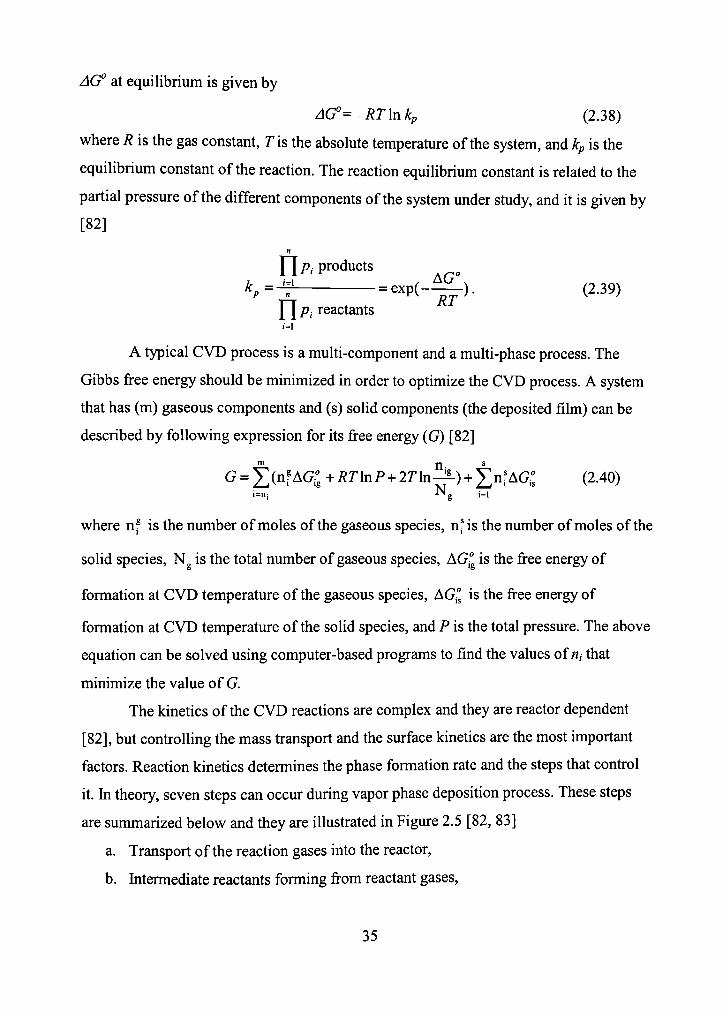
AG° at equilibrium is given by
AG°= RT In kp (2.38)
where R is the gas constant, Tis the absolute temperatiire of the system, and kp is the
equilibrium constant of the reaction. The reaction equilibrium constant is related to the
partial pressure of the different components of the system under study, and it is given by
[82]
n
YlPi products
K =^ = ' ^ P ^ " ^ ^ - ^ - ^ Y\Pi reactants
1=1
A typical CVD process is a multi-component and a multi-phase process. The
Gibbs free energy should be minimized in order to optimize the CVD process. A system
that has (m) gaseous components and (s) solid components (the deposited fihn) can be
described by following expression for its free energy (G) [82]
m n ^ G = X(nfAG° +RTlnP + 2T\n-^) + Y^n\AG:, (2.40)
where nf is the number of moles of the gaseous species, n\ is the number of moles of the
solid species, Ng is the total number of gaseous species, AG° is the free energy of
formation at CVD temperature of the gaseous species, AG° is the free energy of
formation at CVD temperature of the solid species, and P is the total pressure. The above
equation can be solved using computer-based programs to find the values of«, that
minimize the value of G.
The kinetics of the CVD reactions are complex and they are reactor dependent
[82], but controlling the mass fransport and the surface kinetics are the most important
factors. Reaction kinetics determines the phase formation rate and the steps that confrol
it. In theory, seven steps can occur during vapor phase deposition process. These steps
are summarized below and they are illustrated in Figure 2.5 [82, 83]
a. Transport of the reaction gases into the reactor,
b. Intermediate reactants forming from reactant gases,
35
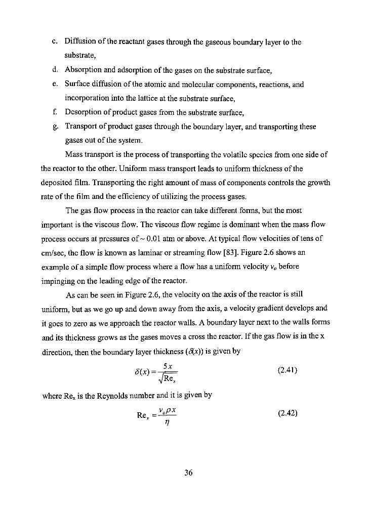
c. Diffusion of the reactant gases through the gaseous boundary layer to the
substrate,
d. Absorption and adsorption of the gases on the substrate surface,
e. Surface diffiision of the atomic and molecular components, reactions, and
incorporation into the lattice at the substrate surface,
f Desorption of product gases from the substrate surface,
g. Transport of product gases through the boundary layer, and transporting these
gases out of the system.
Mass fransport is the process of transporting the volatile species from one side of
the reactor to the other. Uniform mass transport leads to uniform thickness of the
deposited film. Transporting the right amount of mass of components controls the growth
rate of the film and the efficiency of utilizing the process gases.
The gas flow process in the reactor can take different forms, but the most
important is the viscous flow. The viscous flow regime is dominant when the mass flow
process occurs at pressures of ~ 0.01 atm or above. At typical flow velocities of tens of
cm/sec, the flow is knovm as laminar or streaming flow [83]. Figure 2.6 shows an
example of a simple flow process where a flow has a uniform velocity Vo before
impinging on the leading edge of the reactor.
As can be seen in Figure 2.6, the velocity on the axis of the reactor is still
uniform, but as we go up and down away from the axis, a velocity gradient develops and
it goes to zero as we approach the reactor walls. A boundary layer next to the walls forms
and its thickness grows as the gases moves a cross the reactor. If the gas flow is in the x
direction, then the boundary layer thickness {d{x)) is given by
S{x) = 4 ^ (2.41)
where Rex is the Reynolds number and it is given by
R^^=Y^£^ (2.42)
36

where p is the density, and //is the viscosity of the gas in the reactor. The viscosity is a
very important factor in determining the fiictional forces with the reactor walls.
Bulk Gas
— • o _ . ^ ^
Figure 2.5 Illustration of the steps controlling the reaction kinetics in a CVD process. (Adapted from reference [82].)
The average boundary layer thickness for a reactor of length L is given by [83]
(2.43)
where Ret is given by (Reynolds number)
(.>aW)dx = l ^ ^ . l ^ ^
Re^- VoP^ (2.44)
In order to have a proper mass transport to the subsfrate {5) must be as small as
possible. This can be achieved by increasing the flow rate (vo) in the reactor. Re values
are in the hundreds for a typical CVD process, and if the Re is > 2100, then the flow
becomes turbulent [83].
37

2/-oi
'W
-^>\ m — •
— • —w
•
^
— ^ •
^,
7 ^
Tubular reactor walls
Figure 2.6 Laminar flow pattem in a circular tube. (Adapted from [83].)
The mass fransport process is now limited by this boundary layer. The reactant
species has to diffuse through the boundary layer in order to reach the substrate. Using
Pick's low of diffiision, the diffusion flux of component A, J A, through this layer in a
direction x (perpendicular to substrate) is given by [80]
D,^ dc. JA =
'AB (2.45) RT dx
where DAB is the diffiisivity of the reactants, CA is the concentration of component A, R is
the gas constant, and Tis the absolute temperature of the system. The concentration
gradient can be approximated by
dc, Ac -A ^ A _ -c. (2.46) dx Ax 5
where c^ is the concentration of component A in the bulk stream, and c^^ is the
concenfration of component A on the substrate surface. Using the kinetic theory of gases,
3/ /
the diffusivity {D) depends on pressure and temperature as D ~ T'^'^jp [81]. Equation
(2.45) can then be written as
J __DAB (r - .
RT
D AB
RT
PA,-PA (2.47)
where p^^ is the partial pressure of component A in the bulk stream, and p^^ is the partial
pressure of component A at the substrate surface.
38
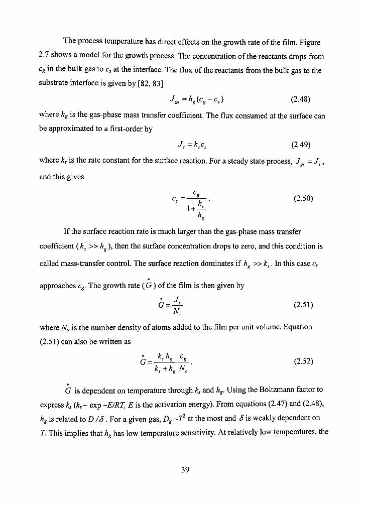
The process temperature has direct effects on the growth rate of the film. Figure
2.7 shows a model for the growth process. The concentration of the reactants drops from
Cg in the bulk gas to c, at the interface. The flux of the reactants from the bulk gas to the
substrate interface is given by [82, 83]
J,s=K^c^-c,) (2.48)
where kg is the gas-phase mass transfer coefficient. The flux consumed at the surface can
be approximated to a first-order by
Js=KCs (2.49)
where ks is the rate constant for the surface reaction. For a steady state process, J ^=J^,
and this gives
Cs=-^- (2.50) 1-1--^
K If the surface reaction rate is much larger than the gas-phase mass fransfer
coefficient (k^ » h^), then the surface concentration drops to zero, and this condition is
called mass-transfer confrol. The surface reaction dominates if /?„ »k.ln this case Cs
approaches Cg. The growth rate (G) of the film is then given by
G = (2.51) A/„
where No is the number density of atoms added to the film per unit voliune. Equation
(2.51) can also be written as
• k h c G = -^^—'-. (2.52)
ks+h,N„
G is dependent on temperature through ks and hg. Using the Boltzmann factor to
express k^ {ks- exp -E/RT, E is the activation energy). From equations (2.47) and (2.48),
kg is related ioD/S. For a given gas, Dg ~f at the most and S is weakly dependent on
T. This implies that hg has low temperature sensitivity. At relatively low temperatures, the
39

surface reactions prevail as dictated by the Boltzmann factor. The growth rate in this case
can IS wntten as G = —-—. At higher temperatures, the film growth process is mainly
GAS
'gs
. - . • .v.
FILM
p
Figure 2.7 Growth process model. The gas flow is perpendicular to the plane of the paper.
confroUed by the mass fransfer or the diffiision of the different components. The film
h„c„ growth rate can be vmtten as G =
A „ for this case.
The thermodynamics and kinetics of the CVD process can be used to develop
models of the film growth process, but due to the complexity of these processes and due
to the number of variables, the trends in the real growth process can be different from
those of the simulation.
As the power coupled to the plasma is increased, the electron density increases in
the plasma. The electron density in the plasma confrols the decomposition reaction rate /?,
as follows [80]
R,=n^k,c (2.53)
where ne is the electron density, A:, is the dissociation reaction rate constant, and c is the
concentration of the reactants. The dissociation reaction rate constant is given by
f 0 \" k..=
v'"./ \E'l\f{E)<j,{E)dE (2.54)
40

where me is the electron mass, E is the electron energy,/(E) is the normalized electron
distribution function, and <T,(£:)is the cross section of the reaction.
The partial pressure [p] of each component of the used source gases is
proportional to its concentration (c). The decomposition rate is proportional to the
decomposition reaction rate. From equation (2.53), it can be seen that increasing either
the power or the partial pressure of the reactant can increase /?,, which in tum increases
the deposition rate [84-86]. The plasma power and the total pressure of the reactor can
confrol the energy of the ions bombarding the substrate which can change the deposited
film nature.
The total chamber pressure and partial pressures of the different components play
an important role in the CVD process. It was mentioned earlier that the partial pressure
[p] of a reactant is proportional to its concentration c. This eventually controls the growth
rate through confroUing the decomposition rate i?,. The partial pressure also has effects on
the final concenfration of the different species in the film [87-89]. The abundance of each
reactant in the CVD chamber is a function of its partial pressure. The total pressure of the
reactor is directly related to the width of the plasma sheath regions. As the pressure goes
down the width of these high field regions grows [78, 80]. This increase in the sheath
width increases the ion bombardment energy on the growing film. This can affect the
growth kinetics, film density, and film cross-linking. Lower total pressure also increases
the mean free path of the plasma species, and this reduces the ionization probability in the
process.
Pumping speed and the flow rate of the process gases controls the residence time
of these components in the active reaction region. The residence time of the active
component should be longer than the characteristic time of the desired reaction [80].
Changing the flow rate of the different components confrols their concenfration in the
CVD chamber. This can change the growth kinetics and film growth rate [90, 91].
The temperature plays an important role in the CVD process. It has a direct effect
on the kinetics of the reactions in the plasma and on the substrate. Temperature also has a
great impact on the diffiision of the different species to and on the subsfrate. Changing
41

the process temperature can change the composition, growth rate and the stresses and
strains in the deposited film [92-93].
2.4 Supercritical Carbon Dioxide (SCCO2) Processes
Supercritical fluids (SCF) are being used as alternative solvents for the hazardous
chemicals. SCFs are also ozone-friendly, inexpensive, do not contribute to smog
problem, provide cleaner extracts, increase reproducibility and improve recovery [95,
96]. A good understanding of this process is a prerequisite for using SCF's efficiently.
Understanding the system parameters (e.g., density, pressure, temperature, extraction
time, etc.) is critical for a successful process. This section will offer the basics of SCF
processes.
Figure 2.8 represents a general phase diagram of the material states. The
supercritical state of any material is attained when the temperature and pressure are raised
above the critical point (critical temperature (Tc) and critical pressure (Pc)). The critical
temperature (Tc) can be defined as the highest temperature at which the gas can be
converted to liquid by increasing the pressure. The critical pressure can also be defined as
the highest pressure at which a liquid can be converted to a gas by increasing the
temperature [95]. SCF's are characterized by physical and thermal properties of both
gases and liquids. The supercritical state is characterized by low viscosity, low surface
tension, high diffusivity, and near liquid molar volumes that result in rapid wetting and
exceUent penetration characteristics [95-102].
42
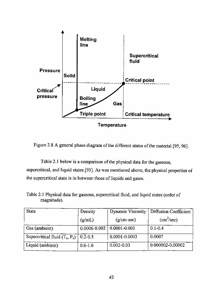
Pressure
Critical pressure
k
Solid
Melting line
Liquid
Boiling ^ ^
Triple point
Gas
Supercritical fluid
Critical point
Critical temperature •
Temperature
Figure 2.8 A general phase diagram of the different states of the material [95, 96].
Table 2.1 below is a comparison of the physical data for the gaseous,
supercritical, and liquid states [95]. As was mentioned above, the physical properties of
the supercritical state is in between those of liquids and gases.
Table 2.1 Physical data for gaseous, supercritical fluid, and liquid states (order of magnitude).
State
Gas (ambient)
Supercritical fluid (Tc, Pc)
Liquid (ambient)
Density
(g/mL)
0.0006-0.002
0.2-0.5
0.6-1.6
Dynamic Viscosity
(g/cm-sec)
0.0001-0.003
0.0001-0.0003
0.002-0.03
Diffiision Coefficient
(cm /sec)
0.1-0.4
0.0007
0.000002-0.00002
43

SCFs can be used as solvents for different purposes. The solvating power of SCF
is a function of the process temperature and pressure. Figure 2.9 shows the relationship
between the solvent power of SCCO2 (measured as the mole fraction of the dissolved
material) and both the pressure and the temperature. The solubility of naphthalene in
SCCO2 is presented in this figure. At lower pressures, the solvent power of SCCO2 goes
dovm as the temperature increase. At higher pressures, the solvent power of SCCO2
increased as the temperature increase. The trend is straight forward if the density, instead
of pressure, was considered. Figure 2.10 shows the relation between the solubility and the
density of the SCCO2. The solvent power of SCCO2 increases as the density of SCCO2
increases. From this figure, we see that the solvent power is better correlated to the
density of SCCO2 than its pressure [95, 97,100]. For CO2, the critical density is 0.47
g/mL and it increases, for example, to 0.96 g/mL at 400 atm pressure at Tc [95]. This
doubling in the density is expected to double the solvent power of SCCO2.
P. Gallagher-Wetmore et al. [100] studied the naphthalene solubility in both
SCCO2 and supercritical ethylene at different pressures. They reported an increase in the
solubility as the process pressure was increased. Due to the changes in the solubility, the
supercritical process can be designed to extract certain components of the material and
also can be used to fractionate the material at different pressures. Figure 2.11 shows how
the solubility of naphthalene in supercritical ethylene changes with the process pressure
and temperature.
44
3S 45 55
Ttmpcrotore T*C
Figure 2.9 Solubility (mole fraction) of naphthalene in CO2 as a function of temperature at different pressures. (Adapted from [95].)
o i — I 0 100 200 300 400 500 600 700 SOO 900
Dtnity p (g/lln)
Figure 2.10 Solubility (mole fraction) of naphthalene in CO2 as a fimction of density at different temperatures. (Adapted from [95].)
45
SCFs also have the advantage of good mass transfer due to their gas like
diffusivity and low viscosity. As was shown in Table 2.1, the SCF diffusivity is
comparable to that of the gas and its viscosity is lower than that of the liquid. Both
diffusivity and viscosity are dependent on the pressure and temperature of the process.
Diffusivity and viscosity approach that of the liquid as the pressure is increased at a
constant temperature. Increasing the temperature increases the diffusivity of the SCF and
decreases its viscosity. Figures 2.12 and 2.13 below show how these factors change with
changing the pressure and temperature. Lower viscosity also leads to small or no surface
tension, which leads to better penefration into the treated samples [95, 100, 101].
Many SCFs can be used as solvents in supercritical extraction processes. Carbon
dioxide is the most suitable of these fluids since it is nontoxic, inflanunable, has modest
critical parameters, commercially available in high purity, environmentally benign, and
inexpensive [95]. Table 2.2 shows the critical parameters for some of the common SCF
[95, 102].
0.1000
1 0.0100
•£
0.0010
0.0001
- " I — \ — 1 1
3 5 K
1 1
1 1 1 1 1 .J 50 too 150 200 250
Prassir* (ahn)
300 350
Figure 2.11 Solubility (mole fraction) of naphthalene ethylene as a fimction of pressure at different temperatures. (Adapted from [95].)
46

10-
10-
u <u
E
I 10- > 3
10 -5
Saturated liquid
^ w i M^Typ'cal diffusivities of solute^s m normal liquids ?ni»S ..,,
_L ± _L 20 40 60 80
Temperature (°C) 100
Figure 2.12 Diffusivity of CO2 as a fimction of temperature at different pressures. (Adapted from [95].)
47

Pressure (atm) 1000
Figure 2.13 Viscosity of CO2 at different temperature and pressures. (Adapted from [95].)
The solubility of SCC02 can be modified and enhanced by adding a miscible,
polar compound to SCF (e.g., methanol). This additional component is usually called a
modifier or a co-solvent [95-102]. The addition of a co-solvent to SCC02 changes the
critical parameter to be in between those of the two components. This can simply be
calculated using the following arithmetic expression [95]
(2.55)
Pc=^co,Pc(co,,-^^n,Pc(™) (2.56)
where ^^o ^^^ ^m ^re the mole fractions of CO2 and cosolvent, respectively [95].
'•c ~ ^ € 0 2 lc (C02) ^ ™ <=(•")
48
Table 2.2 Critical parameters (Tc and Pc) of different
SCFs [95, 101, 102].
Fluid
Carbon dioxide (CO2)
Water (H2O)
Ammonia (NH3)
Nifrous Oxide (N2O)
Nifrogen (N2)
Argon (Ar)
Xenon (Xe)
Propane (CsHg)
Methanol (CH3OH)
Critical
temperature
(°C)
31.0
374.1
132.4
36.5
-147.0
-122.0
16.6
96.8
239.4
Critical
pressure
(psi)
1072
3209
1654
1054
492
706
858
617
1173
The addition of a co-solvent can also have other effects on the supercritical
process. The co-solvent can interact with solute and it can alter the mass transfer and
diffiision coefficients in the mixture. The use of a co-solvent helps to tailor the SCF
process for different applications.
For this research, pure SCC02 extraction and co-solvent modified SCC02 were
used for supercritical treatment processes. In one experiment SCC02 was used to
selectively extract fluorocarbon components from organosilicate matrix in an attempt to
create porous low dielectric constant material. In another experiment, SCC02/co-solvent
system was used for the extraction of poly(propylene glycol) (PPG) porogen from
poly(methylselsisquioxane) (PMSSQ). We also used mixtures of SCC02 and
hexamethyldisilazane (HMDS) to cure plasma-damaged porous low dielectric constant
materials. The details of these experiments will be offered in the proper chapter.
49

The high-pressure system used to perform the supercritical experiments for this
research is a static system consisting of a stainless steel vessel that can handle pressures
up to lOOOOpsi. This vessel is pressurized by a high pressure air-driven Haskel pump. The
vessel assembly is placed in oven that can be used to heat the vessel to temperatures as
high as 200°C. Figure 2.14 shows the schematics of this system. The co-solvent was
directly added to vessel before starting the pressurization process. Both temperature and
pressure can be controlled to suite the experimental needs. The system can also be
evacuated using a mechanical vacuum pump to minimize oxygen content in the system.
To ensure that the system has no oxygen contamination, the system is flushed many times
using CO2 before each experiment.
CO2 Cylinder pressure gauge
?
:o2 Cylii ider
Higli pressure valve
4 High y' \ pressur
- i \ gauge/-
V_J rl^ 1
e
? ~-—J U>*vl
Air-driven High pressure pump
High pressure vent valve
i / ^
Vacuum gauge
T I \ | . ^ To vaniiim pump
High pressure valve
High pressure vessel
Figure 2.14 Schematic diagram of the supercritical system used in this research.
hi order to perform the SCC02 processing in pulse or flow through mode, a new
system was built. Figure 2.15 is a schematic of the new system. This system consists of a
stainless steel chamber designed to handle 16000 psi, a high pressure Haskel booster
pump (20000 psi) is used to pressurize this vessel, and a Jasco liquid injection pump
(operate at pressures up to 7000 psi) is used for co-solvent injection. The chamber
assembly is placed inside an oven which can be heated to 360°C.
50
High pressure gauges
Liquid injection unit
High purity CO2 at 600 psi
V
V5 Vfi
"Wn Exhaust
Separation chamber
V'X High pressure filter
Drive ah High pressure pump Vn: valves
Tc: Thermocouple
Figure 2.15 The schematics of the Maddox lab SCCO2 system.
Vacuum gauge
(V) Vacuum station
The inlet and the outlet lines of this system are heated to improve the solubility of
the co-solvents in SCC02. This is expected to keep the lines clean and free of co-solvents
after the process is complete.
2.5 Optical and Electrical Characterization
In this section, a review of optical and electrical characterization of the film will
be offered. Fourier Transform Infrared Spectroscopy (FTIR) was used to study the
structural properties of the films. Ultraviolet-Visible (UV-Vis) measurements were also
used to study the band gap of the films. The dielectric constant was obtained from
Capacitance-VoUage (CV) measurements.
2.5.1 Fourier Transform Infrared Spectroscopy (FTIR)
Infrared spectroscopy is a powerful tool that allows the identification of unknown
structures. To understand how infrared radiation interacts with material, we need first to
have a quick look at the properties of light. First of all, light can have both wavelike and
51
particles like properties, hi the wave like picture, light is an electromagnetic wave, i.e. it
is a wave with both electric and magnetic fields perpendicular to each other.
The IR radiation occurs in the long wavelength side of the electromagnetic
spectrum as shown in Table 2.3. In IR spectroscopy, wave numbers, in units of cm"', are
usually used in the IR spectrum. The wavenumber can be thought of as a measure of the
number of cycles per cm.
k = ^ = '-A c
(2.58)
where k is the wavenumber, c is the speed of light, X is the wavelength, and vis the
frequency.
Table 2.3 The elecfromagnetic spectrum.
Radiation
Type
Wavenumber
(cm-')
Visible, UV
and X-rays
> 14,000
Near
Infrared
14,000 to
4000
Mid
Infrared
4000 to
400
Far
Infrared
400 to
4
Microwaves
Radio Waves
< 4
In this basic treatment, we will be concerned with the vibrational BR. specfroscopy,
so we will be dealing with radiation in the mid-infrared region (4000 - 400 cm"'). The
energy of molecular vibrations happens to be in this range, which qualify the mid IR
region as a good region for studying these vibrations.
The IR spectiTim can be plotted in different ways, but the most popular ways are
the absorption and transmission spectra. Figure 2.16 shows a comparison between these
two spectra, the IR absorption (fransmission) intensity is plotted as a function of the IR
wavenumber.
Absorbance is defined as follows [103]
^ = log(-^) (2.58)
52

0 . 3 0 -
0 . 2 5 -
0 . 2 0 -
0 . 1 5 -
O <{ 0 . 1 0
0 . 0 5 -
-0 . 0 5 1 — S O O
a - S I C A b s o r p t i o n S p e c t r u m
1000 1500 2000 2500 3000 3500 4000 4500
W a v e r t u m b e r (cm '^)
1 0 0 -
C 8 0
s w C 7 0 ra
50 -
a -S iC T r a n s m i s s i o n S p e c t r u m
p - V ^ ^
- 1 1 • 1 • 1 • 1 • 1 • 1 ' 1 • I '
500 1000 1500 2000 2500 3000 3500 4000 4500
W a v e n u m b e r ( c m ' ' )
Figure 2.16 Comparison between the Absorption and the Transmission spectra of an a-SiC sample.
53

where A is the absorbance, / is the light intensity with the sample in the IR beam (sample
spectiaim), and /<, is the light intensity measured with no sample (background spectrum).
The purpose of measuring /<, is to measure all the contributions from sources other
than the sample (contributions of the spectrometer and the environment to the sample).
Transmission can be defined as follows
T= l/r (2.59)
where 7 is the fransmittance, I and /<, is still the light intensities as were defined above.
From equations (2.58) and (2.59), we get
A = log(i) (2.60)
Absorption measurements can be used to measure the concentration of the IR
active species in the sample. Using Beer's law, which states that absorbance and
concenfration are linearly proportional [101-104].
Consider a radiation of intensity/o is entering a sample of length /. Because some
of the light will be absorbed, the transmitted light intensity, I, is less than Ig. Now
consider a thin shoe of the absorbing sample of thickness, dx, as shown in figure 2.17:
I-dl
dx
Figure 2.17 A slice of thickness {dx) of an absorbing material.
Bouguer and Lambert discovered that the loss in intensity of radiation due to
passing through the slice is (- dT) and it is proportional to the intensity of the incident
radiation, /, as well as the thickness of the slice, {dx) [103-106].
-dl^aldx (2.61)
54
where a is the absorption coefficient. By separating the variables and solving this
differential equation we get
- In / + In /„ = - In [///<,] = a I (2.62)
I/Io = e"'. (2.63)
The absorption coefficient is then given by « = ln{Io/T)ll.
Changing this expression to logarithm to base 10 instead of base e, we get
-2.303 log [///„] = a / (2.64)
\og[I/Io\ = -{a/2.303)l (2.65)
log [///<,] = - a / (2.66)
1 = 10 10-"' (2.67)
where a is called absorptivity and it is given by a = log{Io/I)ll.
According to Beer, the exponent a is proportional to the total quantity of
absorbing material in the path of the beam. Thus
a=c£ (2.68)
where c is the concenfration and £-is the molar absorptivity fin liter / mol. cm).
Combining equations (2.59), (2.65), and (2.68) we get
T = I/Io = IO-''' (2.69)
A=-\og(T) = scl. (2.70)
Equation (2.70) is often knovm as the Beer's law.
The absorption coefficient (a) can be calculated using the Lambert-Beer law a =
ln(/</7)//. The base line corrected IR spectra can then be fitted to Gaussian distiibutions to
find the area under these peaks, which in tum gives the integrated absorption of the band.
It is known that the concentration of the bonds (AO is directly proportional to the
integrated absorption intensity of the band as seen in the following equation:
N=c {^^dco=CI (2.71) "' CO
where C is a proportionality constant (reciprocal cross section of a given vibrational
mode) and / i s the integrated absorption intensity [107-111]. Equation (2.71) can be
approximated by
55

N=— {a{Q})dco (2.72)
where «„ is the center band wave number. Typical values of this constant are given
below [108]
C(si-H)-1.4xl0^°cm-^
C(c-H)=1.35x 10^'cm"^
C(si.c) = 2.13xl0'^cm"^
C(Si-o)=1.5x 10'^cm"l
When a molecule absorbs IR radiation, it vibrates in different ways. The bonds
can sfretch, contract, and bend. Figure 2.18 shows the fundamental vibrations that can be
observed for a molecule [106]. The molecular vibrations due to IR absorption are very
complex, but they can be broken down to limited number of vibrations corresponding to
normal modes of vibration of the bonds in the molecule. The number of normal modes
can be determined from the available degrees of freedom for this molecule. If a system
has N molecules, then 3N coordinates needed to describe the system. If we consider the
molecules to be rigid, then the number of needed coordinates to describe the system can
be reduced to 3N - 3. Since the vibrational degrees of freedom is to be counted here, then
the rotational degrees of freedom can be subfracted and this leaves 3N - 5 degrees of
freedom for the linear molecules and 3N - 6 degrees of freedom for the non-linear
molecules.
In order for a molecule to absorb IR radiation it should satisfy two necessary
conditions. First the molecule should possess a dipole moment {ju), which can be simply
defined by the product of the charge and the distance separating the charges:
M = rq (2.73)
where ju is the magnitude of the dipole moment, r is the distance between charges, and q
is the charge.
56
Plane O - ^ Stretching vibration (v)
Plane <s> y j \ hi plane bend (5) ^^ + out of the page
- into the page
Out of plane bend (y)
Rock: in plane bend (p)
Wag: out of plane bend (x)
Twist (T)
Figure 2.18 Fundamental molecular vibrations possible for a molecule. The response of the molecules to IR radiations will be in the form of one of these vibrations.
57

Bend symmetrical
Bend asymmetrical
Bend asymmetrica
Deformation in plane Deformation out of plane
Figure 2.18 (Continued).
Considering atoms in molecules as balls connected by springs, and if the
molecules have a dipole moment, then due to the wave nature of the elecfromagnetic
radiation, the molecules will start to vibrate and the electromagnetic wave energy is
absorbed. The dipole moment of the molecule can be a permanent dipole moment or an
induced dipole moment as was discussed in Chapter I. In both cases the molecules will
interact with the IR radiation. To state the first condition in a more accurate way we can
58

say that for a molecule to absorb IR radiation, it must have a vibration during which the
change in the dipole moment with respect to the distance is non-zero:
^ ? t 0 . (2.74) dx
So any molecular vibration that satisfies this condition is said to be IR active. It is
also important to notice that the intensity of the IR radiation is directly proportional to
{—Y, this will be discussed later. dx
For bound molecules, the vibrations are quantized, and there are certain allowed
vibrational states. Figure 2.19 is a simple representation of the vibrational states of a
molecule. This implies the second necessary condition for IR absorption; the energy of
the IR impinging on the molecule must be equal to the energy difference between the
vibrational energy levels for that molecule. Most species in the universe have a band
corresponding for the first vibrational state in the range 4000 - 400 cm"' [103], and
because of that most molecules can be identified from the transition between their ground
vibrational state and their first state. Transitions between the ground state and states
higher than the first vibrational state are possible and they are called overtones and they
usually occur at much higher wavenumber range [103, 104, 111].
To understand the conditions for IR absorption and the necessary selection rules
imposed on the IR spectrum, let us consider a diatomic molecule. If the reduced mass (i )
of this molecule is given by:
l/^=l/mi+l/m2. (2.75)
Then the kinetic energy of this molecule is given by:
T = i / , ^ ( ^ ) ^ = p ^ / 2 ^ (2.76) dt
59

where p is the conjugate momentum and q is the displacement of the molecule. Assuming
a simple harmonic oscillator potential:
V=ViKq^ (2.77)
where K is the force constant for the vibration.
Then the Schrodinger equation becomes
- J : , _ ^ ( ^ _ _ ^ , . ) ^ . 0 . (2.78)
This equation can be solved for the well-known harmonic oscillator solution:
E^=hv{v-\--) = hck{v + -) (2.79)
where k — is the wave number, and v is the vibrational quantum number. 27t c\ f^
The corresponding vibrational eigenfimctions are
W.= ', ^ e / HX-^q) (2.80) V2^v!
271-J uK j— .1, where a = — , and the H^-sja q) are the Hermite polynomials of the v degree.
h
To get more accurate representation, anharmonicity terms should be added to the
potential energy term. One-way to look at the force constant A" is as a measure of the
curvature of the potential well near the equilibrium position:
d^V K = (^)t,^o- (2-81)
dq
60

Energy Rotational level
Vibrational level
4lotational levels Vibrational level
Distance between
Figure 2.19 Transitions between the vibrational states. Energy levels are not to scale.
The selection rule for the IR spectrum can be determined by the following integral
[104, 105]:
[/ ].V' = \<' (Qa) M ^." (Qa) dQ„ (2.82)
where ju is the dipole moment in the electronic ground state (fransition moment), y/ is the
vibrational eigenfiinction (equation (2.80), W^ are the vibrational quantum numbers
corresponding to the transition, and Qa is the normal coordinates. If one of this integral's
components is not zero, then the vibration associated with Qa is IR active [105].
For the simple harmonic case, we can express the dipole moment of the molecule
in a Taylor series:
,dju, 1 ^d^ju. 2 , /'=/', M f ) . - + ^ ( ^ ) . - +•••
(2.83)
where the subscript e refers to the equilibrium configuration, and x is the displacement of
the intemuclear distance from equilibrium. Then from (2.80) and (2.82) we get:
[//],V' = ^e kl' ." ^ + (^)^ Vv' ^ ." ^ + - (2.85)
61

Since [f/^, and y/^,, are eigenfimctions of the same Hamiltonian, they are
necessarily orthogonal, which means that for / # / ,
j ^ ; \l/^„ dx = 0 (2.85)
and
[/"].V' =("^)^ K ' < v" • + "" (2-86)
The first term of (2.84) is non-zero only if Jv = i- / , and this constitute the
transition between vibrational states selection rule. Since Av refers to v^pper - viower, the
selection rule is effectively zlv=7.The transitions intensities are dependent also on
I [ju]^,^„ I ^ and therefore, according to (2.86), on {—f.
dx
It is easy to judge if this integral is zero or not by considering the symmetry in the
molecule, and because of that, the group theory does play a role in understanding IR
specfroscopy. The non-zero components will correspond to a certain transitions between
the vibrational states and this transition corresponds to a wavenumber that determines
the peak position in the IR spectrum.
The peaks in an IR spectrum have different intensities. The first factor that
determines the peak intensity is the magnitude of the change in the dipole moment ( — ) ,
dx
which is different for the different molecules. The second factor that determines the peak
intensity is the concentration of the molecules in the sample as we have seen in Beer's
law {A = -log (T) = sc I). The absorptivity {s) of the material is proportional to (—)^ dx
and it is an absolute measure for IR absorption for a specific molecule.
The peak width in the IR spectrum, originates from the intermolecular
interactions. Since the samples we are dealing with consists of many molecules, and these
molecules exist in different chemical environments and they interact with their
environment in different ways. This kind of interaction has a direct effect on the
electronic configuration in the molecule, which in tum affects the force constants
62
between the atoms in different molecules and this will change the wavenumber at which
the molecule will absorb the IR radiation. Then the absorption will happen at a range of
wavenumbers instead of absorption at one wave numbers, and this creates the peak width.
In the coarse of this research three different materials were studied using FTIR
the tiiple phase a-SiC:H/SiO/C:H film, organosihcate (fluorinated and nonfluorinated),
and methylselsisquioxane (MSSQ) based organosilicate films. The corresponding FTIR
active bands that can be detected in these films are summarized in Table 2.4 below [112-
121].
Table 2.4 FTIR active bands for materials used during this research.
Bond species -Si-H„,n=l,2, 3 -Si-H2 -Si-H -Si-H„ -Si-(CH3)n,n=l,2,3 -Si-(CH3)n,n=l,2,3 Si-O-Si and Si-O-C Si-0 cage structure or short chain Si-0 Si-C C=C Si-F Si-F2 Si-Fs SiF4 CH2 (symmetric)
CH2 (asymmetric)
CH3 (symmetric)
CH3 (asymmetric)
C-H C-H Free OH Bonded OH
Wavenumber (cm"') 2000 - 2250 885 - 895 800 - 845 460 - 680 1240 -1280 760 - 870 1020-1090 1120-1190 430 - 450 730 - 780 1590 - 1625 820 - 920 915-945 860-910 -1015 2830-2855
2920 - 2925
2860 - 2875
2955 -2975
3000 - 3050 2890 - 2900 3580 - 3670 3230-3590
Bond type Stretch Wag Wag Rock Deformation Rock, Wag or Stretch Stretch Deformation, Stretch Rock stretch Wag or Stretch Stretch Stretch Stretch Stretch Stretch (bend at -1450) Stretch (bend at -1450) Stretch (bend at -1375) Stretch (bend at -1470) Stretch Stretch Stretch Stretch
63

2.5.2 Ultraviolet-Visible (UV-Vis) Absorption
UV-Vis absorption measurements were used for band gap measurements of some
of the samples used during this work. J. Tauc developed a model for the optical
absorption of amorphous solids [122]. Amorphous materials can be defined as any
isofropic solid in which three-dimensional periodicity (long-range order) is absent [122].
According to Tauc observations, amorphous solids cannot be completely random
as the case in the gas phase. The binding forces in crystals can achieve the long-range
order, while in case of amorphous material; these forces achieve order only at distances
of the order of the lattice constant (short-range order), hi amorphous solids, the short-
range order includes the neighboring atoms within the first coordination number. The
stiiicture of amorphous materials is complex. Theories like the existence of small crystals
(crystallites) and the continuous models were used in an attempt to understand these
materials.
As atoms in the solid attain long-range order (crystalline materials) or short-range
order (as in the case of amorphous materials), their wavefunctions overlap. Due to this
overlapping, and because of Pauli's exclusion principle, the band structure emerges [123-
126]. In some amorphous systems, a gap in the band structure appears. The states in the
lower energy band usually are filled and this band is called the valence band. While, the
upper band with empty or sparsely populated states is called the conduction band. If an
electric field is applied, then the electrons in the conduction band will be able to move
because of the empty (or the sparsely-populated) states, and thus the material can conduct
current. An energy gap is formed between the valence and conduction band, the size of
this gap is the main factor that controls whether the material is a metal, insulator or a
semiconductor. The density-of-states {g(E)), number of energy states in the interval E
and E+dE, for a typical material with a band structure is shown in Figure 2.20.
Having impurities in the material under investigation infroduces new states. The
impurity can be in the form of a substitutional atom, an interstitial atom, or a vacancy.
The substitutional atom shares electrons with the other atoms around it. It can be a donor
64

g(E)
Ey Ec
Figure 2.20 Change in the density of states near the band gap. Energy (£)
atom where it gives elecfrons to the crystal, or it can be an acceptor atom where it shares
the existing crystal elecfrons. In the case of interstitial impurities, an atom is positioned
in between the crystal atoms, and its outer electrons are shared with the crystal. This
makes the interstitial impurity a donor. The vacancy is just an empty site in the ordered
structure, and this missing atoms from this site deprives the structure from electrons,
which makes the vacancy an acceptor. These different types of impurities perturb the
bands and introduce new levels in the band structure. Due to this perturbation, impurity
band introduces the effect of the band tailing where states are now extended to energy
gap as show in Figure 2.21. Donors and acceptors exert forces on the conduction
electrons and the valence holes creating this tailing effect.
When electrons in the valence band are excited with the proper energy, they can
be elevated to the conduction band. The energy given to the valence electrons should be
equal to the band gap energy for this to happen. For most amorphous material this energy
is in the range of the UV and visible light. Tauc developed a systematic model to estimate
this energy [81,103, 114, 125, 126]. Since this is basically an absorption process, then
65

we can use the absorption formalism developed earlier in this chapter. The absorption
process can be due to direct transition or an indirect transition. For a direct transition, as
shown in the band diagram in Figure 2.22, the momentum is conserved and the initial and
final state of this transition are related as follows
E^=hv-\E. (2.87)
where E/is the final energy state, £, is the initial energy state, and /j vis the energy of the
used excitation light.
g(E
Ey Ec Energy {E) Figure 2.21 Band-tailing effect as seen in the density of states diagram.
Considering parabolic bands, and using their corresponding energies, the
absorption coefficient, equation (2.65), attributed to the band gap of an amorphous
material is given by the Tauc's equation [125]
a{hv) = A'{hv-E^f
where Eg is the band gap energy, and A * is given by
^ « •
m. +m. 'h ^ '"e
nch m„
(2.88)
(2.89)
66
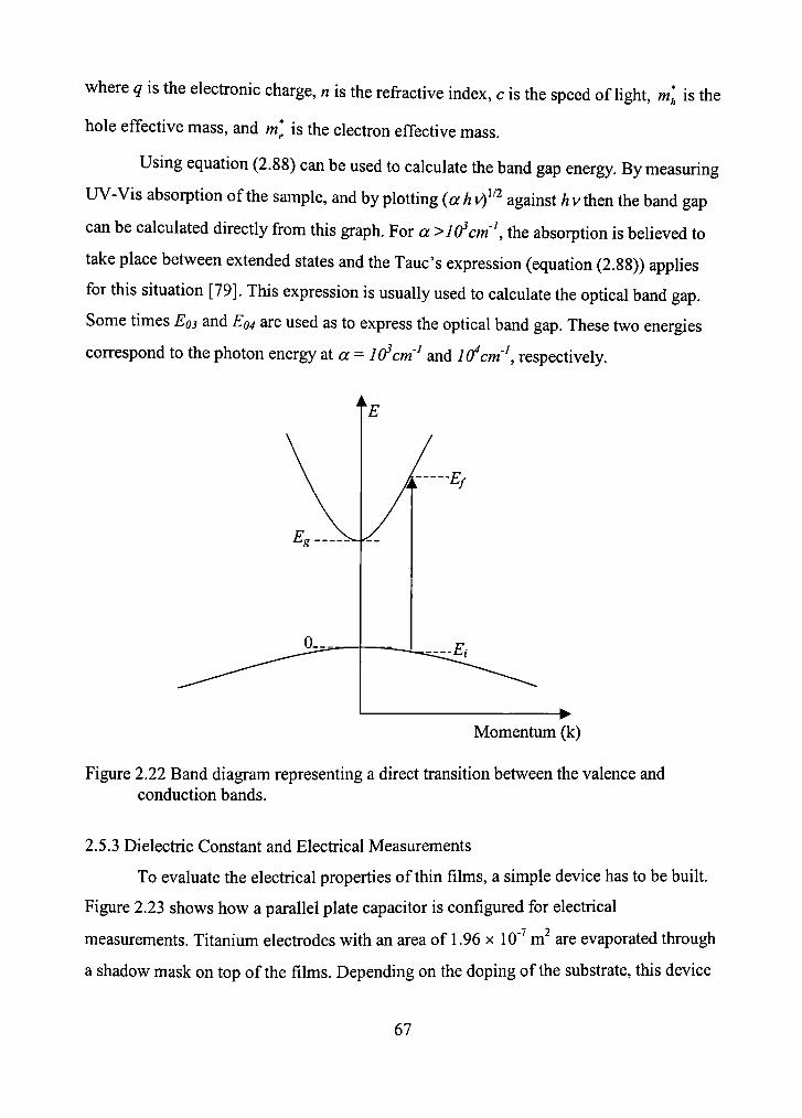
where q is the elecfronic charge, n is the refractive index, c is the speed of light, nC, is the
hole effective mass, and w* is the electron effective mass.
Using equation (2.88) can be used to calculate the band gap energy. By measuring
UV-Vis absorption of the sample, and by plotting {a h vf'^ against hvihen the band gap
can be calculated directly from this graph. For a >l&cm', the absorption is believed to
take place between extended states and the Tauc's expression (equation (2.88)) applies
for this situation [79]. This expression is usually used to calculate the optical band gap.
Some times E03 and E04 are used as to express the optical band gap. These two energies
correspond to the photon energy at « = l(fcm' and W^cm', respectively.
Momentum (k)
Figure 2.22 Band diagram representing a direct fransition between the valence and conduction bands.
2.5.3 Dielectric Constant and Electrical Measurements
To evaluate the electrical properties of thin films, a simple device has to be built.
Figure 2.23 shows how a parallel plate capacitor is configured for electrical
measurements. Titanium elecfrodes with an area of 1.96 x 10" m^ are evaporated through
a shadow mask on top of the films. Depending on the doping of the subsfrate, this device
67

can be used to measure the dielectric constant, current-voltage (FV), and capacitance-
voltage (CV) characteristics of the films under inspection. A heavily doped (low
resistivity) subsfrate were used to build the parallel plate capacitor necessary for
dielectric constant measurement, while lightly doped (high resistivity) substrate was used
for CV measurements.
Using the simple parallel plate capacitor relation, the dielectric constant can be
calculated directly from capacitance values (saturation capacitance in the case of CV
measurement). The capacitance of a parallel plate capacitor is given by [75, 127]
k£„A C = (2.91)
where C is the measured capacitance, k is the dielectric constant of the material under
study. So is the free space permittivity (8.85 x 10"' F/m), and t is the film thickness.
Ti electrodes -4
Film
Figure 2.23 The setup for CV or IV electrical measurements. For capacitance measurements on heavily doped substrate on of the probing terminals is placed on the substrate.
2.5.4 Porosity Calculation
For the porous films under study, it is important to estimate the films' porosity
[126]. The dielectric constant values for porous material are proportional to their
porosity. A simple method developed by K. P. Mogilnikove et al. [129] was adapted for
porosity estimation for the samples used during this work.
68

hi this method, ellipsometiic porosimetry is used for the estimation of the pore
size distribution in the films. Changes in the film thickness and refractive index are used
as the basis for this calculation. By relating the optical characteristics and the material
composition, this model is able to predict the pore volume in the film [128,129]. Using
Clausius-Mossotti equation (equation (2.17) in the beginning of this chapter), which
relates the molecular polarizability {y„oi) of the material directly to its refractive index at
optical frequencies, /moi is also proportional to the polarizability of a unit volume through
the Lorentz-Lorenz equation (equation (2.18)):
" = ^ ' ' • ' ' - = 4 . ( „ ^ . 2 ) < " ' >
where B is the polarizability of a unit volume, Nj is the number of molecules, /„„! is the
molecular polarizability, and n is the refractive index of the material. Then the pore
volume can be calculated from:
T^ 1 porous Jilm -j pore ~ ~^ ~ ^~
nonporous film in]+ 2) i.nl-\) (nl + 2) (2.92)
where «„ is the refractive index of the film after pressurization (porous film), and nt, is
the refractive index of the nanoporous host matrix. In this model, the volume of the film
is normalized to unity, and the pore size is measured relative to this volume. The
accuracy in finding the pore volume depends on the accuracy of measuring the refractive
index of the films. Using a prism coupler to measure the refractive index of the films
gives a ± 0.01-0.02 accuracy in measuring the pores voliune. The refractive index can
also be replaced with the dielectric constant values for this calculation (see equation
(2.17)). The pore volume plays an essential role in calculating the effective dielectric
constant [130, 131] as will be seen in Chapter FV.
2.5.5 Prism Coupler
During this work, prism coupler was used for thickness and refractive index
measurements. The principle of prism coupling depends on the attenuated total reflection
phenomenon, where an evanescent elecfromagnetic wave is allowed to propagate along
69

the interface of two semi-infinite media. Figure 2.24 shows the details of a prism coupler
measurement. Three conditions are necessary for coupling [132-133]
1. The angle of incidence of the laser beam should be such that the evanescent field
phase velocity in the gap is equal to the phase velocity of the mode to be excited.
2. The beam polarization should be similar to the polarization of the mode to be
excited.
3. The gap between the film and the prism base is of the order of a half wavelength.
The accuracy of thickness measurement using prism coupling is about
o
± 0.5%+50 A, while the accuracy of refractive index measurement is about ± 0.001.
Detector
3 0 0
in g 250 H
2 0 0 -
1 0 0
t = 1 . 2 0 1 3 nm n = 1.5656
1 0 0 0 5 0 0 — I 1 1 • 1 • 1 • I ' I - 5 0 0 - 1 0 0 0 - 1 5 0 0 - 2 0 0 0 - 2 5 0 0 - 3 0 0 0
Table Posi t ion
Figure 2.24 The schematics of a prism coupler and an example of one measurement using this technique.
70
CHAPTER m
NANOPOROUS TRIPLE-PHASE a-SiC:H/SiO/C:H LOW-k FE.MS
The present work reports plasma-enhanced chemical vapor deposition (PECVD)
of a-SiC:H/SiO/C:H films using mixtures of diethylsilane (C4Hi2Si) and methane (CH4).
The properties of these films were studied by prism coupler, Fourier transform infrared
specfroscopy (FTIR) and dielectiic constant measurements. The objective of this study is
to use supercritical carbon dioxide (SCCO2) and annealing treatments to suitably modify
the dielectiic properties of tiiple phase films. The dielectiic properties can be tailored by
selectively removing one of the three phases and/or changing the concentration of the
different phases. The effects of precursor concentrations and RF power on the dielectric
properties and composition of these films are also investigated.
3.1 The Experiment
Triple-phase (or triple-components) a-SiC:H/ SiO/ C:H films were deposited in a
parallel-plate radio-frequency (RF) PECVD reactor. A 13.56 MHz RF power generator
was used to sustain the plasma. The schematic diagram of this CVD chamber was
presented in Figure 2.8 in Chapter n. The PECVD chamber was pumped down to a base
pressure of 2 x 10" Torr using a combination of turbo-molecular and mechanical pumps.
Lightly doped and heavily doped silicon substrates with resistivities of 37.5 - 62.5 Q cm
and 0.005 - 0.01 Q cm, respectively, were placed on the grounded electrode (anode).
Films on lightly doped p-type (100) Si subsfrates were used for the Fourier transform
infrared (FTIR) spectroscopy while the films on heavily doped Si subsfrates were used
for capacitance measurements.
Mixtures of diethylsilane (C4Hi2Si) and methane (CH4) were used to deposit the
a-SiC:H/SiO/C:H films with thickness ranging from 0.6 to 1 \xm. The flow rates of gases
were varied to get different gas flow ratios (R) in the mixture, where R = {[SiC4Hi2] /
([SiC4Hi2]+ [CH4])}*100% was varied between 1.96% and 5%. The deposition pressure
and temperature were maintained constant at 300 mTorr and 50°C, respectively, for all
71
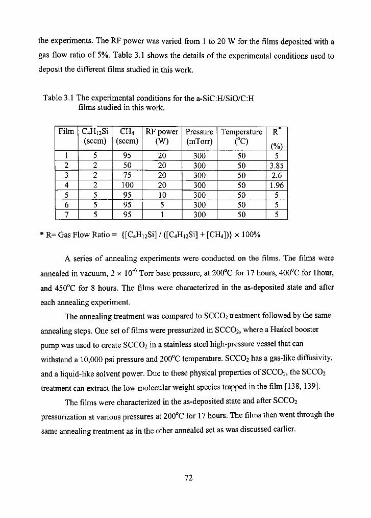
the experiments. The RF power was varied from 1 to 20 W for the films deposited with a
gas flow ratio of 5%. Table 3.1 shows the details of the experimental conditions used to
deposit the different films studied in this work.
Table 3.1 The experimental conditions for the a-SiC:H/SiO/C:H films studied in this work.
Film
1 2 3 4 5 6 7
C4Hi2Si (seem)
5 2 2 2 5 5 5
CH4 (seem)
95 50 75 100 95 95 95
RF power (W)
20 20 20 20 10 5 1
Pressure (mTorr)
300 300 300 300 300 300 300
Temperature (°C)
50 50 50 50 50 50 50
R*
(%) 5
3.85 2.6 1.96
5 5 5
* R= Gas Flow Ratio = {[C4Hi2Si] / ([C4Hi2Si] + [CH4])} x 100%
A series of annealing experiments were conducted on the films. The films were
annealed in vacuum, 2 x 10" Torr base pressure, at 200°C for 17 hours, 400°C for Ihour,
and 450°C for 8 hours. The films were characterized in the as-deposited state and after
each annealing experiment.
The annealing treatment was compared to SCCO2 treatment followed by the same
annealing steps. One set of films were pressurized in SCCO2, where a Haskel booster
pump was used to create SCCO2 in a stainless steel high-pressure vessel that can
withstand a 10,000 psi pressure and 200°C temperatiire. SCCO2 has a gas-like diffiisivity,
and a liquid-like solvent power. Due to these physical properties of SCCO2, the SCCO2
treatment can extract the low molecular weight species frapped in the film [138, 139].
The films were characterized in the as-deposited state and after SCCO2
pressurization at various pressures at 200°C for 17 hours. The films then went through the
same annealing treatment as in the other annealed set as was discussed earlier.
72

The structure of the films was studied using a Perkin-Elmer 1600 series FTIR
specfrometer. The absorption coefficient {a) was calculated using Lambert-Beer law
(equation (2.70) Chapter II), a = ln(V7)//, where /„ is the zero absorption baseline, / i s
the film's measured fransmittance, and / is the film's thickness in cm. The baseline
corrected IR spectra were fitted to Gaussian distributions in an attempt to get the
corresponding areas of the different bands. These fits were then used to calculate the
integrated absorption of each band. It is known that the concentration of the bonds (AO is
directly proportional to the integrated absorption intensity of the corresponding band as
seen in the following equation (equation (2.72) in Chapter A):
N=C \-^-!-dco=CI (3.1)
•' 0)
where C is a proportionality constant and / i s the integrated absorption intensity [140].
Errors in concenfi-ation were calculated based on the standard deviation of several
Gaussian fits of the same data. Errors in the concentration calculations of various bonds
in the fihn using equation (3.1) were estimated to be in the range 1.7 to 3.75%. The
refractive index and thickness of the films were measured using Metricon 2010 prism
coupler. The dielectric constant of the films was measured at 10 KHz on
metal/insulator/Si structure using a heavily doped Si (low resistivity) subsfrate as the
bottom electrode and an E-beam evaporated Ti elecfrodes (with a 1.96 x 10" m^ area) as
the top elecfrode.
3.2 Annealing Treatinent of a-SiC:H/SiO/C:H Films
Figure 3.1 shows the FTIR spectrum for film #3. This FTIR spectrum shows
absorption peaks corresponding to SiC stretching vibrational mode at 790 cm"', SiO
stretching at 1045 cm"', SiCHs bending at 1256 cm"', CHn (n=2,3) bending at 1450 cm"',
C=0 stretching at 1712 cm"', SiHn sfretching at 2100 cm"', CHn (n=2,3) stretching in the
region from 2800 to 3000 cm"', and -OH stretching at 3445 cm"' [124, 85, 141, 87, 142,
143,144]. Even though no oxygen was used during deposition, the films show the
presence of Si-0 band (1045 cm"' peak). This could be either due to the presence of small
73
amounts of moisture and/or oxygen in the system or due to the reaction with oxygen and
moisture after the films were taken out of the PECVD chamber. Since the FTIR spectra
recorded immediately after deposition shows the stretching vibrations of the Si-0 bonds
at 1045 cm" , then this is a clear indication of the existence of oxygen and/or moisture in
the CVD system. Thus, a base pressure of 2 x 10' Torr was not enough to eliminate
oxygen and water vapor from the chamber. Also, exposing the films to ambient air for
few days resulted in a reduction in the refractive index values. For freshly deposited film
the refractive index was about 1.63 and it decreased to 1.52 for the same film exposed to
ambient air for about one month. These facts confirm that the SiO bonds in the films are
due to both contributions; (i) reaction with oxygen and/or moisture during deposition and
(ii) reaction with oxygen and moisture when films are exposed to the laboratory ambient.
The reactivity of the films with air is attributed to the existence of free radicals, which
upon exposure to air, start to react with oxygen and moisture. The incorporation of
oxygen causes the formation of SiO phase in the film along with a-SiC:H and a-C:H
phases, leading to a triple-phase (triple-component) film. Figure 3.1 (a) indicates the
existence of the three phases (or the three components); the SiC phase at around 790
cm"', SiO phase at around 1045 cm"', and the C:H phase at around 2900 cm"'. In order to
reduce the effects of air exposure, the measurements were carried out on freshly
deposited samples. Annealing the films to higher temperature also allows the free radicals
in the film to react with oxygen and this increases the concentration of SiO bonds as
shown in Figure 3.2.The presence of oxygen in the films was also verified using
Rutherford Back Scattering (RBS) analysis of film # 1.
74
E
c 0)
"5 E o o o c o
o (0
<
20 00-
1500-
1000-
500
0
5 0 0 0-1
40 00
3000-1
20 0 0
1000-
0 -
(a ) A s d e p o s ite d fi lm # 3 ( b ) 4 5 0 ° C a n n e a l e d f i lm # 3
( b ) Jk. 4 0 0 0 3 0 0 0 2 0 0 0 1 0 0 0
W a v e n u m b e r ( c m '^)
^
Figure 3.1 FTIR spectra of (a) as-deposited and (b) 450°C annealed a-SiC:H/ SiO/ C:H film.
E o^ c .2 re
C 0)
o c o o O
900,000
800,000 -
700,000
600,000 -
500,000
400,000
300,000
200,000
500
A n n e a l i n g T e m p e r a t u r e ( C )
Figure 3.2 Changes in the SiO concentration after the different annealing temperatures.
75

The Si and CHn concentrations in the films is dependent on the gas flow ratio R.
Figure 3.3 and Figure 3.4 are examples of the Gaussian fits for the CHn band. The four
peaks used to fit this band are CH2 symmetric at 2840 cm"', CH3 symmetiic at 2875 cm"',
CH2 asymmetric at 2910 cm"', and CH3 asymmetric at 2955 cm"'. Figure 3.5 shows the
variation in the concentration of CHn bonds from the band extending from 2800 to 3000
cm"', SiCHs bonds from the 1256 cm"' band, SiHn bonds from the 2100 cm"' band and
SiO bonds from the 1045 cm"' band as a function of R. Although the CHn absorption
(2800 to 3000 cm"') has contiibutions from Si-CHn and C-CHn bonds, it is believed that
the C-CHn absorption is significantly higher than Si-CHn absorption for the films
deposited at 50°C. This observation can further be supported by the fact that as R (or
diethylsilane flow rate) increases the CHn concentration in the film decreases.
-200 2750 2800 2850 2900 2950 3000
Wavenumber (cm' )
3050 3100
Figure 3.3 The Gaussian fitting of the CHn band for the as-deposited fihn.
76
500 -
"_ 400 -O
4 ^ C .* 300 -u
ffi
« o U 200 -c 2 '^ a. S 100 -(0
.Q <
0 -
450
'
"C anneale
/
1 '
d film
1
#3
\ '/ X. 'J
'" v-< •'
'J
'
If' \
f » / V / \\ / V
/ V
I
u
\ \\ \\ \\ \ \
1 • 1 2800 2850 2900 2950 3000
W avenum ber (cm' ' )
3050
Figure 3.4 The Gaussian fitting of the CHn band for film # 3 after 450°C annealing.
Increasing the flow rate of diethylsilane in the precursor gases increases the
concenfration of the Si radicals at the expense of C in the plasma. The increase in the Si
concenfration increases SiHn, SiO, and SiCHs concentration in the film at the expense of
CHn. The fact that the CHn mainly comes from C-CHn can also be supported by noticing
that; even though the CHn concentration is decreasing as the annealing temperature is
increased, the SiCHa concenfration is almost independent of annealing temperatiire (see
Figure 3.10 below). The polarizability of the film is a function of the concenfration of the
different components of the film. The electronic polarizability of the SiC and the SiO is
higher than that of the CHn components, hicreasing the concentration of the Si radicals
increases both the SiC and the SiO concentration at the expense of the CHn concentration
and this in tum increases the polarizability of the film. This increase in the elecfronic
polarizability increases the dielectric constant of the films as seen in Figure 3.6.
Figure 3.7 shows the effect of RF power on CHn, SiCHs, and SiHn concenfrations
for R - 5% films. Again, this figure shows that as the RF power increased the Si
77

concenfration is increased and the CHn concentration is decreased. High RF power is
more effective in fragmenting the C4Hi2Si, which produces more Si radicals. The effect
of the increase in Si incorporation and the decrease in CHn concentration on the dielectric
constant of the films is shown in Figure 3.8. The dielectric constant increased from 3.52
to 4.23 as the power is increased from IW to 20W. The films deposited at higher power
were mechanically harder (more scratch resistant). Increasing the RF power improves the
crosslinking in film and leads to harder films.
The annealing cycles have a great effect on the structural and dielectric properties
of the films. Figure 3.9 shows that annealing at 200°C caused a small increase in the
thickness, but the subsequent annealing steps caused the thickness to decrease. Structural
changes upon heating cause thickness expansion and evolution of trapped gases and free
radicals [145]. Figure 3.10 shows the effect of annealing on CHn, SiCHs, SiH, C=0, and
OH bond concenfration. There is a significant decrease in the concentration of SiH and
CHn bonds while the concentration of SiCHs bonds remains almost constant and the SiO
concentration (Figure 3.2) increases when the films are annealed from 200°C to 450°C.
78

400,000
320,000
O (/) 240,000
160,000
1.5 2.0 2.5 3.0 3.5 4.0 4.5 5.0 30,000
» 28,000
O W 26,000
24,000 1.5 2.0 2.5 3.0 3.5 4.0 4.5 5.0
58,000
56,000
^ 54,000
52,000 / •'
•-—
/
/
_ — — — " — •
1.5 2.0 2.5 3.0 3.5 4.0 4.5 5.0
170,000
.c 160,000
^ 150,000
140,000
2.0 2.5 3.0 3.5 4.0 4.5 5.0
Gas Flow Ratio (R)
Figure 3.5 Effect of gas flow ratio (R) on the concenfration (arb. units) of SiO, SiCHs, SiHn, and CHn bonds.
79
2* c m "w c o u _o 'C «rf
o a> o a
5.00 -
4 .75 -
4 .50 -
4 .25 -
4 .00 -* - — ^
G a s 3 Flow
4 Rat io (R )
Figure 3.6 Effect of gas flow ratio (R) on the dielectric constant of the as-deposited films.
We believe that annealing at higher temperature removes C-CHn phase leaving
behind nanopores or molecular-size free volume and reducing the over all film thickness
by 14.5%. Having nanopores in the film lowers the dielectric constant considerably by
infroducing more free space into the bulk of the film. Since the concentration of Si-CHs
bonds in the film remained almost same (Figure3.10), it also helps in maintaining the
dielectric constant to lower values. The Si-CHs reduces the polarizability and the film
density due to the steric hindrance of the methyl group [51].
Figure 3.11 shows the effect of annealing on the refractive index of the fihns. The
decrease in refractive index as the annealing temperatiire is increased is attributed to the
removal of CHn groups from the film and the formation of nanopores or molecular-size
free volume. The black circle in this figure shows the effect of SCCO2 freatment at 200°C
on the refractive index of the sample, and this will be discussed later.
80
210,000
180,000 c
O 150,000
120,000-
\ . •
• "—
v>
10 15
5 10 15
Power (W)
20
CO
X
o V)
20,000
16,000
12,000 • — • --'^
m
^ m
--
T ' 1
20
Figure 3.7 Effect of RF power on the concentration (arb. units) of CHn, SiHn, and SiCHs bonds.
81
5 1 0 1 5
P o w e r (W )
Figure 3.8 Effect of RF power on the dielectric constant of the as-deposited films.
0 . 7 2 -
E a. w 0 . 6 8 0) c U
0 . 6 4 -
0 1 0 0 2 0 0 3 0 0 4 0 0 5 0 0
A n n e a l i n g T e r n p e r a tu re ( C )
Figure 3.9 Changes in thickness of film #3 after the different amiealing temperatiues.
82
150,000
2 60,000-c
§ 30,000-O
100 200 300 400 50
Annealing Temperature ( C)
Figure 3.10 Effect of the different annealing temperatures on the concenfration of CHn, OH, SiHn, SiCHs, and C=0 bonds in the fihns.
Figure 3.12 presents the effect of annealing on the dielectric constant of the film.
The k value did not change much after the first annealing at 200°C. Annealing of the
fihns at 450°C reduced the k values to 2.13 and 2.36 for the films deposited with R =
2.6% and R = 5% respectively. This can be explained by the removal of CHn from the
films. As mentioned before, this decrease is due to the introduction of nanopores in the
films. Similar observations were made by Grill and Patel [53] and they also reported that
the formation of nanopores was the primary factor in reducing the dielectric constant in
their fihn. SEM measurements of these films after annealing indicate that the pores are
beyond the measurement resolution (the SEM used for this measurement has a -100 nm
resolution). This fact implies that the pores have a nanometer size. The effect of SCCO2
treatment at 200°C (black circle in Figure 3.12) will be discussed later.
83

Annealing at high temperature also removes the broad OH band at about
3445cm"' and the carbonyl (C=0) band at about 1712 cm"' as seen in Figure 3.1 (b) and
Figure 3.10 This removal of the highly polar OH and C=0 reduces the polarizabihty of
the film, thereby reducing the dielectiic constant fiirther. We believe that by optimizing
the deposition and the amiealing conditions it is possible to obtain dielectric constant
values as low as 2.1 for the triple phase organosilicate films.
1.60
X
o 1 1.55^ .1 ' • * • '
2 1.50-1
1.45
S C C O j treated sam pie at 8300 psi
100 200 300 400 500
Anneal ing Temperature ( C)
Figure 3.11 Effect of the different annealing temperatures on the refractive index.
84

4.5
3.5-
^ 4.0 c (0 (A C o o o 1 3.0 0)
o 2.5
2.0
S C C 0 2 T r e a t e d s a m p l e at 8300 psi
R = 5% R = 2.6%
100 200 300 400
A n n e a l i n g t e m p e r a t u r e ( C)
50
Figure 3.12 Effect of the different annealing temperatures on the dielectric constant (k) of films 1 and 3.
3.3 SCC02/Annealing Treatment of the a-SiC:H/SiO/C:H Films
The impact of the SCCO2 pressurization followed by armealing cycles was
evaluated in this experiment. The films were pressurized at 1060psi, 4470 psi, and 8300
psi for 17 hours while maintaining the temperature constant at 200°C. Another set of
samples were annealed in the same vessel (high-pressure vessel) and also, in a vacuum
chamber at 200°C for 17 hours to differentiate the effect of SCCO2 treatment from
annealing treatment. It is interesting to note that significant change in refractive index and
dielectric constant were observed only for films treated at 8300 psi. The black circles in
Figures 3.11 and 3.12 show the effect of 200°C, 8300 psi SCCO2 treatment on the
refractive index and k, respectively. This 21% decrease in the dielectiic constant may be
due to the extraction of CHn species by SCCO2. It seems that the high solvent power at
85

8300 psi is necessary for the SCCO2 to dissolve CHn species. Since 400°C and 450°C
annealing reduces the dielectric constant fiuiher, SCCO2 treatment was not sufficient for
the complete removal of the CHn species. Our fiiture goal is to use SCC02/co-solvent
system for the efficient removal of CHn species at low temperatures and pressures and at
shorter times.
86

CHAPTER IV
LOW-k ORGANOSILICATE FILMS
A new liquid precursor, tetravinylteframethylcyclotetrasiloxane (TVTMCTS),
was used to prepare low dielectiic constant films. PECVD was used to deposit these films
with hydrogen (H2) as the carrier gas for the TVTMCTS. TVTMCTS has a ring stiiicture
that can help to lower the dielectric constant if preserved. Figure 4.1 shoes the structure
of the TVTMCTS molecule.
The basic structure of organosihcate film is composed of a silicon-oxygen
backbone with methyl (CH3) incorporation. The methyl groups make a robust structure
leading to a less dense film and may resuh in a lower k. These films can be deposited by
either spin coating or plasma-enhanced chemical vapor deposition (PECVD) techniques
[51, 55, 148]. The PECVD method is often preferred since it is industry standard and
hence its use would facilitate incorporation of a new material. For PECVD organosilicate
fihns, deposition is done using either a SiH4/hydrocarbon gas mixtures or liquid sources.
In an attempt to introduce porosity and reduce the dielectric constant, fluorinated
organosilicate films were deposited from mixtures of TVTMCTS and C4F8. Supercritical
carbon dioxide (SCCO2) treatment can effectively remove amorphous fluorocarbon (a-
F:C) films. Using SCCO2 to selectively remove the a-F:C phase from the fluorinated
organosilicate film, porosity can be introduced to the treated film.
87
^ V3 CH = CH2
ySi 0 CH2=CH^ I I CH3
0 s/ \si-o/'^CH = CH2
Figure 4.1 The structure of TVTMCTS precursor.
4.1 TVTMCTS Organosilicate Films
Organosilicate films with thicknesses ranging from 0.7 to 1.5 |xm were deposited
using a capacitively-coupled plasma-enhanced chemical vapor deposition (PECVD)
apparatus driven by a RF supply of 13.56 MHz [75]. The liquid TVTMCTS was
delivered to the chamber with H2 (20 seem) as a carrier gas since the liquid has a low
value of vapor pressure to produce self-sustaining plasma. The gas line connecting the
chamber and liquid reservoir was heated at 60°C to prevent condensation. Two sets of
deposition conditions were used. In the first set, the samples were prepared at a
deposition temperature of 23°C and the pressure was varied from 0.15 to 1.75 Torr. For
the second set, the deposition temperatures (To) ranged from 23 to 400°C, while the
pressure was kept constant at 1.5 Torr. The RF power was also kept constant at a lowest
possible value of 3 W to prevent breaking up of the ring structiire, thus retaining it in the
PECVD film. The films were deposited simultaneously on p-type Si (100) with
resistivities of 0.008 ~ 0.02 Q cm and 40 ~ 60 Q cm and quartz subsfrates for
measurements of dielectric constant, refractive index, Fourier transform-infrared specfra
(FTIR) and optical band gap respectively. For the measurement of the dielectric constant,
Ti electrodes with an area of 0.196 im^ were deposited by an e-beam evaporation system
on the organosilicate dielectric film deposited on heavily doped silicon substrates. The
capacitance of the structure was measured at a frequency of 10 KHz. The film thickness
was measured using a prism coupler with a standard deviation of 1%, Metricon Model
88
2010. The FTIR and UV-visible absorption spectra were measured using a Perkin-Ehner
Model 1600 spectrometer and Shimadzu Model IJV-2501PC spectrophotometer,
respectively. The infrared absorption spectra of these films were recorded in the range of
400-4000 cm" and corrected for substrate absorption. The absorption coefficient (a) was
computed applying Lambert-Beer's law. For detailed analysis, the baseline corrected IR
specfra were fitted to Gaussian distributions and the area under the peak is directly
proportional to the concentration of the bonds. The adhesion of the films was tested using
a simple tape test. The films deposited at room temperature and at different pressures
were annealed under vacuum for one hour at temperatures from 10°C to 500°C to test the
thermal stability. These films were annealed one week after deposition and were kept at
ambient conditions during that period. Measurements were made immediately after
annealing and then the same samples were annealed again at a higher temperature. The
samples were exposed to ambient during measurements that took about three hours.
Figure 4.2 shows the FTIR specfra of the TVTMCTS liquid and a PECVD film
deposited at 1.5 Torr and room temperature. The major peaks for both the source and the
PECVD film have been identified and are listed in Table 4.1. As stated earlier, it is
comprised of a cyclic Si-O-Si with methyl and vinyl groups attached to each Si atom. The
Si-0 vibration, the most intense absorption band at 950 -1200 cm"' was present in both
spectra [51, 55, 90]. We will show later that this absorption band is due to three distinct
vibrations and that the most intense mode arises from the Si-O-Si cyclic stiiicture. Thus,
the Si-O-Si main structure of the liquid is preserved after the plasma polymerization
under the deposition conditions used for this sample, hi addition, the bands centered at
764 cm"' and 1261 cm' , corresponding to the rocking and bending modes of Si-CHs,
respectively, are also observed in both the hquid and PECVD film [124, 148-151].
Further comparison of the two samples shows that absorption bands due to vinyl groups
peak at 960, 1408, 3018 and 3056 cm"' for CH2 vibrations and 1598 cm"' for C=C in Si-
CH=CH2 [124, 151] observed in source spectrum are not present in the PECVD film
spectrum as indicated in Table 4.1. The C=C bonds of the vinyl group are broken during
the plasma decomposition process, hi addition, absorption bands centered at 2854 cm"'
89

(CH2)sym and 2878 cm"' (CH3)sym [152] in the PECVD films are not observed in the
liquid. The liquid source spectrum does not have any OH related bands usually found at
3350 cm"' and 3650 cm"' [90, 150] and these bands are also not observed in the PECVD
film. Hence, the films we deposited were OH-free films. The vibrational bands at 1720
cm"' and 2150cm"' corresponding to C=0 and SiH bonds [90] are also not observed in
either the source or the film spectra.
Figure 4.3 shows the dielectric constant and the concentration of Si-CHs bonds of
the as-deposited films as a function of deposition pressure with temperature fixed at 23
°C. With increasing pressure the dielectric constant decreased from a value of 2.92 for
0.15 Torr to 2.65 for 1.75 Torr whereas the Si-CHs bonds increase over the same range.
The results for films deposited at different temperatures and at a constant pressure of 1.5
Torr are shown in Figure 4.4.
Table 4.1 Identification of IR absorption in TVTMCTS and PECVD films.
Wavenumber (cm"')
TVTMCTS
764, 1261
796, 1010, 1075
960, 1408
1598
- , 2904
- , 2963
3019,3056
PECVD
761, 1260
790, 1010, 1065
" ) ~ j *"
-
2854,2918
2878, 2960
" J ~
Attributed source
(Si-CH3)roc, (Si-CH3)bend
Si-Obend, Si-Ostr(linear), Si-Ostr(ring)
CH2 in vinyl (wag, bend)
C=C in Si-CH=CH2
(CH2)sym> (CH2)asym
(.>--H3)sym) (. -113)35x111
CH2 in vinyl (sym, asym)
References
124,151,152
90,151,152
124,152
124,152
152
153
153
90

2 5-i
'to'
•E 2 . 0 -3
. Q
3, 1.5-<u o ro 1.0-
O CO
^ 0 . 5 -
0 0 -20
i^ 0 2-, c
•e ra, 0.1
8 1 0.0
PECVD f l l n i / ^ - - V
M 3150 3000 2850 2700 / 1 < Wavenumber ( c m ' ) / 1
PECVD film A y \ A
00 1500 1000 W a v e n u m b e r (cm"^)
—J 500
Figure 4.2 IR spectra of the liquid TVTMCTS and the PECVD film. A magnified comparison of the CHn (n = 2,3) band is shown on the upper right.
The dielectric constant is almost unchanged at a value of 2.70 over the
temperature range from 23 up to 200 °C but it increases as the temperature is raised above
300 °C as shown in Figure 4.4a. The Si-CH3 absorption intensity on the other hand is
constant and then decreases at higher temperatures. Apparently at higher deposition
temperatures, the weaker Si-CH3 bonds break leaving the films with a lower
concenfration of these bonds. The data shown in Figure 4.3 and Figure 4.4 indicate an
inverse association between the concentration of Si-CH3 bonds and the dielectric constant
in agreement with the results of other researchers [51, 148, 151].
91

^ 3.1 c I 3.0-1 8 2.9 o 'S 2.8 o f 2.7 ° 2.6^
o I
(?) c o (0
c u c o o
65000-1
.-I 60000
; 55000-1
50000-(/)
•a O 45000
40000
7-J3 = 23 °C
(a) H 1 H
(b)
0.0
H h
0.5 1.0 1.5 Pressure (Torr)
2.0
Figure 4.3 Behavior of the dielectric constant and concentration of Si-CH3 bonds as a function of deposition pressure.
92

3.1
5 3.0 tf>
8 2.9 o 'B 2.8 o _2 .2 2.7 Q
2.6-1
70000
•A xi 60000
50000-
40000-
30000
o • V) > * -o c o
^ i '
re 1^
ncen
t
(/> 4.^
3
.a re CA
bond
o O 20000
• 1 • 1 r-
Pressure = 1.5 Torr
f (a)
(b)
-I 1 . (.
100 200 300 400 Deposition Temperature (°C)
Figure 4.4 Behavior of the dielectric constant and concentration of Si-CH3 bonds as a function of deposition temperature.
Figiue 4.5 shows the Gaussian fit of the Si-O band in the frequency range of 950
cm"' to 1225 cm"' for the PECVD film. The spectra shown here are those of films
deposited at room temperature and at 0.6 Torr (solid line) and at 1.75 Torr (broken line),
both at a TD of 23°C. Each spectrum was fitted with three Gaussian curves centered at
around 1000, 1065 and 1105 cm"', respectively. The most intense of the three is the 1065
cm"' band. The splitting of the Si-0 band into 1000 cm"' and 1065 cm"' is not usually
seen in other organosilicate films; often only the peak around 1065 cm' is present [51,
55]. In the work of T. Fujii et al. [142] on organosihcate films prepared using a siloxane
source (HMDSO), they attributed the 1000 to 1100 cm"' band to siloxane bonds but did
93
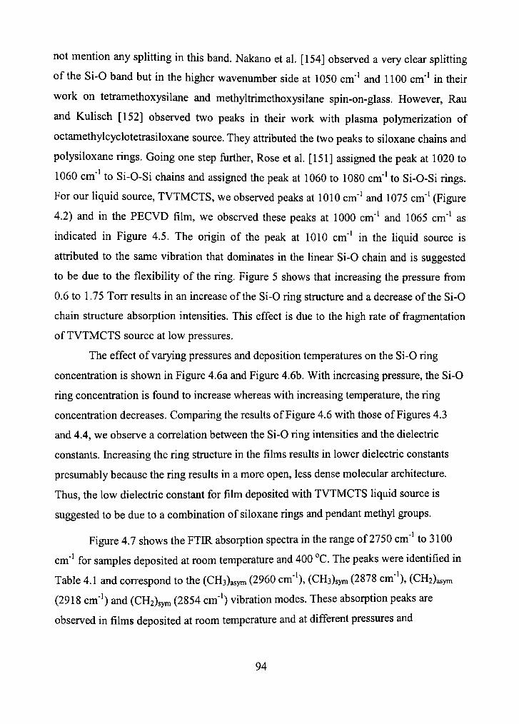
not mention any splitting in this band. Nakano et al. [154] observed a very clear splitting
of the Si-0 band but in the higher wavenumber side at 1050 cm"' and 1100 cm"' in their
work on tetramethoxysilane and methyltrimethoxysilane spin-on-glass. However, Rau
and Kulisch [152] observed two peaks in their work with plasma polymerization of
octamethylcyclotefrasiloxane source. They attributed the two peaks to siloxane chains and
polysiloxane rings. Going one step fiirther. Rose et al. [151] assigned the peak at 1020 to
1060 cm"' to Si-O-Si chains and assigned the peak at 1060 to 1080 cm"' to Si-O-Si rings.
For our liquid source, TVTMCTS, we observed peaks at 1010 cm"' and 1075 cm"' (Figure
4.2) and in the PECVD film, we observed these peaks at 1000 cm"' and 1065 cm"' as
indicated in Figure 4.5. The origin of the peak at 1010 cm"' in the liquid source is
attiibuted to the same vibration that dominates in the linear Si-O chain and is suggested
to be due to the flexibility of the ring. Figure 5 shows that increasing the pressure from
0.6 to 1.75 Torr results in an increase of the Si-O ring structure and a decrease of the Si-O
chain structure absorption intensities. This effect is due to the high rate of fragmentation
of TVTMCTS source at low pressures.
The effect of varying pressures and deposition temperatures on the Si-O ring
concenfration is shown in Figure 4.6a and Figure 4.6b. With increasing pressure, the Si-O
ring concenfration is found to increase whereas with increasing temperature, the ring
concenfration decreases. Comparing the resuhs of Figure 4.6 with those of Figures 4.3
and 4.4, we observe a correlation between the Si-O ring intensities and the dielectric
constants. Increasing the ring structure in the films resuhs in lower dielectric constants
presumably because the ring results in a more open, less dense molecular architecture.
Thus, the low dielectric constant for film deposited with TVTMCTS liquid source is
suggested to be due to a combination of siloxane rings and pendant methyl groups.
Figure 4.7 shows the FTIR absorption spectra in the range of 2750 cm"' to 3100
cm"' for samples deposited at room temperature and 400 °C. The peaks were identified in
Table 4.1 and correspond to the (CH3)asym (2960 cm"'), (CH3)syni (2878 cm"'), (CH2)asym
(2918 cm"') and (CH2)sym (2854 cm"') vibration modes. These absorption peaks are
observed in films deposited at room temperature and at different pressures and
94

temperatures. However, at a deposition temperature of 400 °C, the (CH2)sym at 2854 cm"'
was not present (Figure 4.7). The CH bond concentrations are shown in Figure 4.8. With
increasing pressures, the CH2 and CH3 concentration were found to increase. This
behavior of these bonds was found to be the same as those of Si-CH3 bonds in Figure
4.3b. This clearly indicates that the CHn (n = 2, 3) vibrations are from CHn group bonded
to Si and not from C-CHn bands.
T^SOOO -\ E
^ 6 0 0 0 H o u § 4 0 0 0 -
§ 2 0 0 0 -.Q <
0 A
0.60 Torr
1.75 Torr
1200 1100 1000 W a v e n u m b e r (cm'^)
900
Figure 4.5 Gaussian curve fit of the Si-O band for two films deposited at 0.6 Torr and 1.75 Torr. Each spectrum is fitted with three Gaussian curves.
95

c
O j2 'S> I O £ i « ? | 4-1 C c o 0) ^ o c o o
c
O J2
i « • | |
4-1 C C O 0) ^ o c o o
600000-
500000-
400000-
T^ = 23 "C
• 1 1
' 1 1 ' 1 »
(a)
0.0 0.5 1.0 1.5 Pressure (Torr)
600000
450000-
300000-
150000- (b) ' 1 —
— • 1 1 1 1 1
Pressure = 1.5 Torr
-
^^^
— • 1 • 1 • 1
100 200 300 400 Deposition temperature (°C)
Figure 4.6 Concentration of Si-O (ring) bonds as a function of deposition pressure and temperature.
96
^^1250 "E ^1000 -0) O 750
.1 500 a o 250 w
< 0 ^
Pressure = 1.5 Torr
23 °C
3100 3000 2900 2800
Wavenumber (cm' )
Figure 4.7 Comparison of the CHn (n = 2,3) absorption bands for films deposited at 23 and 400°C.
The optical absorption spectra for the liquid and the PECVD film deposited at
1 Torr and room temperature are shown in Figure 4.9. The absorption increases gradually
at a photon energy of 4.1 eV and then rapidly increases at 4.8 eV for both spectra. The
estimated band gap from the Tauc [125, 155] plot for the film is about 4.6 eV. The
similar behavior of the two spectra provides fiirther support to our IR analysis that the
main structure of the liquid is preserved after the plasma polymerization. Figure 4.10
shows the optical band gap of the films as a function of pressure and deposition
temperature, respectively. The band gap of the films deposited with different pressures
appears to remain constant at a value of 4.5 eV. However, for films deposited with
varying deposition temperature, the band gap decreased with increasing To and the value
decreased up to a value of 2.5 eV for T\ = 400°C.
97

(A 4-1
'E 3 re
(0 c 0)
c o
o (A
(A
100000
90000
80000
40000^
30000
0.0
.•t: 100000 c 3 si re
(A c 0)
c o
o (A
80000-
0.5 1.0 1.5 Pressure (Torr)
100 200 Deposition temperature ("C)
300 400 0 /
Figure 4.8 Absorption intensity of CHn (n ==2,3) bonds as a fimction of deposition pressure and temperature.
98

5.0 -
4 . 0 -
3.0 -
2.0 -
1.0-
0 . 0 -
1 1 1 1 1
PFCVn film / TVTMCTS source
1 '
\ l --_^ y -^--^x y y
0.5
0.4
0.3
0.2
0.1
0.0
2 4 6 P h o t o n Energy (eV)
Figure 4.9 UV-visible spectra of TVTMCTS and PECVD film.
0.0 0.5 1.0 1.5 Pressure (Torr)
100 200 300 400 Deposition temperature (°C)
Figure 4.10 Optical band gap of PECVD films as a fimction of deposition pressure and temperature.
99

The thermal stability of the films was investigated by annealing the films in
vacuum. Figure 4.11 shows the plot of the dielectric constant as a function of annealing
temperature {TA) for the film deposited at 1 Torr and 23°C. The film was found to have a
stable k up to TA = 400°C and then it decreased to 2.50 at TA = 500°C. The thickness of
the film also remained stable up to T^ = 400°C and then decreased by about 30% when
the film was annealed at 500°C. Figure 4.12 confirms that the film is structurally stable
up to 400°C as the concenfration of the Si-CH3 and Si-O bonds almost remained the
same up to 400°C. There is a significant decrease in their concentration when the sample
is armealed at 500°C. The films did not show any signs of cracks typical for films with
excessive stress up to TA of 400°C.
The refractive index of the films measured by the prism coupler ranges from 1.45
to 1.47. The films show excellent adhesion to the subsfrates based from results of tape
test performed on all samples.
3.1
3.0
« 2.9 (A
8 2.8 u £ 2.7-i u o> .S 2.6 Q
2.5
2.4
as-deposited
t f ^ ^
1 Torr, 23 X
100 200 300 400 500 Annealing temperature (°C)
Figure 4.11 Variation of the dielectric constant of the PECVD film with respect to annealing temperature.
100

X O ^ 54000-.' w 5) ••=
• i o . 52000-C .Q O h •— (0
S u) 50000-= 1 * o c -o 48000-o o
46000-
— • 1 • 1
(a) ^ ^
• •
1 Torr, 23 "C
— - • 1 • 1 1
1 1 1 1 1 1
• ^ \ \ \ \ \ \
\ : \ i •
< — 1 • — 1 — • — — 1 —
100 200 300 400 500 Annealing temperature (°C)
O) ,c 600000-
V --s 550000-•JT C W 3 < o .Q 500000-
o ^^ '^ « 450000-
^ c ? o g -Q 400000-
o O 350000-
• 1 • 1 —
(b)
•- •
1 Torr, 23 °C
1 ' 1
— I 1 1
•
- > 1 1
1 1 • 1
•
\ \ \ •
\ \ -1 1
1 -1 • 1
100 200 300 400 500 Annealing temperature (°C)
Figure 4.12 Variation of the Si-CHs and Si-O bonds of the PECVD films with respect to annealing temperature.
4.2 SCCO2 Treatment of Fluorinated Organosilicate Films
In this section we present a method for reducing the dielectric constant by
supercritical CO2 pressurization (SCCO2) of plasma-enhanced chemical vapor deposition
(PECVD) fihns. The goal of this method is to create nanopores in the films by exfracting
un-bonded and loosely bonded low molecular weight and CO2 soluble species by SCCO2
treatment. This is similar to removing CHn in dual phased SiCOH and organic film
through thermal annealing, thus creating voids and hence low-k [53]. At temperatures and
pressures greater than 31 °C and 1070 psi, respectively, CO2 becomes supercritical and
acts like a liquid solvent. The solvent-like property of SCCO2 with a mixtiire of co
l d
solvent has been used by Los Alamos National Laboratory to successfiiUy remove
photoresist and it produced virtually no hazardous wastes [156]. Several groups of
researchers have studied the solubility of polymers in SCCO2 [139, 157-161]. High
molecular weight species are generally insoluble in CO2 unless there are strong specific
interactions between the CO2 and the polymer. For example, high molecular weight
perfluoropolymers [162], hydrofluorocarbon polymers [163], and chlorofluorocarbon
polymers [139] have been found to be soluble in CO2. On the other hand, oligomers and
low molecular weight compounds are often soluble, especially those containing CO2-
philic groups, such as siloxanes and perfluoro groups [164]. We have performed studies
of the effect of SCCO2 treatinent on PECVD deposited fluorocarbon (a-C:F) films using
C4F8 gas. The films dissolved in SCCO2.
hi the previous section, we investigated low k organosilicate films using a liquid
source, tefravinylteframethylcyclotetrasiloxane (TVTMCTS). This source has an open
stinicture and we have succeeded in preserving the ring structure after plasma
polymerization using PECVD. These films were stable after CO2 pressurization up to
9000 psi and pressurization temperatures up to 200°C. These stable properties make this
film a good matiix from which CO2 soluble species can be extracted. The methodology
of the present study is as follows; A composite film is deposited mainly of TVTMCTS
organosilicate film and of low molecular weight a-C:F loosely bonded or unbonded to the
organosilicate main structure [76]. Since a-C:F film dissolved with pressurization, we
speculated that a-C:F incorporation and removal by SCCO2 would create nano or
molecular scale porosity without adversely affecting the mechanical integrity or thermal
stability of the matrix. To facilitate this experiment, C4F8 gas is mixed in the TVTMCTS
and H2 plasma. The composite film is then exposed to post deposition SCCO2 freatment.
The organosihcate and a-C:F composite films with thickness of 0.75 to 1.75 /xm
were deposited on p-type Si (0.008 ~ 0.02 Q cm and 40 ~ 60 Q cm resistivities) and
quartz substrates in our PECVD system. As stated above, we used TVTMCTS liquid
source with H2 as carrier gas to deposit the organosilicate film and added C4F8 gas in the
plasma to fabricate a composite film. The experimental conditions for five films that will
102

be used for analysis throughout this work are listed in Table 4.2. The RF power was kept
as low as possible to prevent the ring structure of the TVTMCTS source from breaking
since the rings provide an open structure and is the main reason for low-k in the
TVTMCTS films [53]. All films were deposited at RT and the C4F8 flow rate was varied
to obtain films with different CF^ concentrations. A film with conditions similar to Film 2
but without C4F8 gas was also fabricated for comparison (Film 4). Film 5 is an a-C:F film
and was used to show the solubility of a-C:F in SCCO2.
The SCCO2 extraction process was performed as follows; the as-deposited films
(about 2 X 2 cm dimension) were placed inside a small cylindrical stainless steel pressure
chamber with inner diameter of 2.5 cm, outer diameter of 10.2 cm, and depth of 12.7 cm.
The ambient air was then pumped out for several minutes using a roughing pump. The
chamber temperature was then ramped slowly to achieve the desired pressurization
Table 4.2 Deposition Conditions of TVTMCTS organosilicate films.
Film
1
2
3
4
5
TVTMCTS+H2
(seem)
20
20
20
20
0
C2F2
(seem)
20
3
0.5
0
40
RF power
(W)
6
3
10
3
50
Pressure
(Torr)
0.3
0.3
1.0
0.3
0.3
Temperature
CO 25
25
25
25
25
temperature of 200°C. The chamber was subsequently pressurized isothermally with CO2
(99.999%) using a gas booster pump (Haskel) driven by air at 70 psi. The pressure of the
chamber was then maintained at 8650 psi for eight hours. After the extraction was
completed, the vessel was depressurized to 500 psi and the temperature was ramped
down to RT. Depressurization was completed at RT.
103

hi addition to the SCCO2 extraction studies, we compared SCCO2 treated and
thermally annealed films. Annealing without SCCO2 was done in a vacuum chamber in
N2 atmosphere for 8 hours at 600 mTorr.
Measurements of Fourier transform infrared spectroscopy (FTIR), thickness and k
were performed for as-deposited and SCCO2 treated samples. The FTIR spectra were
measured using a Perkin-Elmer Model 1600 spectrometer. The capacitance of the film
was measured at 10 KHz.
Table 4.3 shows the effect of SCCO2 treatment on the thickness and dielectric
constant for films 1- 4 listed in Table 4.2. The dielectric constants of the composite fihns
after CO2 exfraction at 8650 psi at 200°C for 8 hours were reduced by 10 to 14 %. As a
comparison, in Table 4.4, where the films (fresh set of Fihns 1- 4) were only annealed at
200°C for 8 hours in N2, we observed that there is no significant change in either k or
thickness. However, the k and thickness of Film 4 deposited without C4F8 were
unchanged in both treatments. Thus, the supercritical CO2 pressurization treatment is a
good method to reduce the k value of the composite films.
104

Table 4.3 Effect of SCCO2 at 8650 psi, 200°C, 8 hrs
Film
1
2
3
4
Thickness (^m)
1.7441+0.021
1.5194± 0.019
0.7533± 0.015
0.7285+0.010
0.7543+ 0.007
0.6791+0.018
1.1860+0.0148
1.1860+0.0148
k
2.87+0.10
2.48+0.09
14.0% decrease
3.82+0.14
3.34+0.09
12.5% decrease
3.42+0.10
3.07+0.09
10.2% decreased
2.71+0.05
2.71+0.05
no change
Treatment
As-deposited
SCCO2
As-deposited
SCCO2
As-deposited
SCCO2
As-deposited
SCCO2
Table 4.4 Effect of annealing at 200°C, 8 h in N2 without SCCO2.
Film
1
2
3
4
Thickness {\xm)
1.8117+0.015
1.8057+0.019
0.8627+0.016
0.8614+0.021
0.8841+0.033
0.8613+0.029
1.1860+0.0148
1.1860+0.0148
k + 0.1
2.87
2.87
no change
3.82
3.82
no change
3.42
3.42
no change
2.71
2.71
no change
Treatment
As-deposited
Annealed at 200°C
As-deposited
Annealed at 200°C
As-deposited
Annealed at 200''C
As-deposited
Annealed at 200°C
105

The ability of SCCO2 to dissolve a-C:F films is demonstrated by comparing the
FTIR spectra of an a-C:F film (Film 5 in Table 4.2), as-deposited and after subsequent
SCCO2 treatinent as shown in Figure 4.13. The broad absorption band from 400 to 1400
cm"' is typical of a soft, highly disordered and low cross-linked a-C:F polymer fihn. After
the film was pressurized at 2500 psi and 200°C for 10 hr, the C-F absorption band
intensity is almost negligible as seen in Figure 4.13. Initially, the as-deposited fihn had a
thickness of about 1 pm and it decreased significantly after SCCO2. Thus, SCCO2
dissolved the a-C:F film. However, a-C:F films deposited with the same conditions but at
higher temperatures did not dissolve in SCCO2 presumably because of higher cross-
linking density. The addition of gases like H2 in C4F8 during deposition also produced a
highly cross-linked a-C:F films that have higher resistance to SCCO2 treatment.
^ 1.0
• | 0.8
^ o.6^
^ 0.4 OJ
O 0.2
< 0.0
as-deposited
n ' r 1400 1200 1000 800 600 400
Wavenuinber(cm' )
Figure 4.13 FTIR spectra of as-deposited and SCCO2 a-C:F fihn.
The FTIR specfra of organosilicate films deposited with and without C4F8
incorporation (Films 2 and 4) are shown in Figure 4.14. We have attributed in detail the
106
absorption bands of the organosilicate film without C4F8 in a previous section. The
addition of fluorocarbon in the film gives rise to a Si-F band centered at 900 cm"', hi
addition, the band around 945 to 1220 cm"' attributed to Si-O in the TVTMCTS spectrum
becomes broad and extended to the frequency range of 1250 cm"'. In fact the FWHM of
this band increased from 395 to 474 cm"'. The Si-0 band position also shifts to higher
wave number due to the addition of fluorine. Figure 4.15 shows a close up of the
normalized Si-0 band to see this shift. Comparing Figures 4.13, 4.14 and 4.15, the Si-0
absorption band for the TVTMCTS film observed at 945 to 1220 cm"' is found to overiap
with the C-F bands for a-C:F film at 600 to 1400 cm"' (Figure 4.13). Thus, the increase in
FWHM of the Si-0 band for the composite film is due to additional C-F bands along with
the Si-0 (linear) and Si-0 (ring) bonds at the high wavenumber side. As can be observed
from Figure 4.14, it is clear that the Si-0 and Si-CHs absorption intensities were reduced
significantly with C4F8 addition. Further inspection shows that the CH group also
reduced. Thus, incorporation of CF species adversely affects the robust structure of the
organosilicate films by breaking Si-0 (rings and chains) and replacing O and CH3 bonded
to Si with F. Breaking of Si-0 rings and lower Si-CH3 bond concentration is expected to
enhance the fihn density and hence increase the dielectric constants. The addition of F to
the Si02 structure (i.e., formation of Si-F) is normally expected to decrease the dielectric
constant, but the contrary is observed here. For the same deposition conditions, the
addition of C4F8 increases the k for TVTMCTS film from 2.71 (Film 4) to 3.82 (Film 2).
In the previous section, we claimed that the main reason for the decrease in k in the
TVTMCTS organosilicate film is the open stmctiire provided by the TVTMCTS and the
robust methyl groups resulting in a less dense film. For the composite film studied here,
we speculate that the expected decrease in k contributed by the addition of Si-F was
offset by the increase in k due to the large reduction in the Si-0 ring stiiictures and Si-
CH3 concentration. However as more C4F8 is added in the case of Film 1 the dielectric
constant reduces. This is because the composite film now consists mostly of a-C:F with
some organosilicate incorporation. A pure a-C:F film can have a dielectric constant as
107
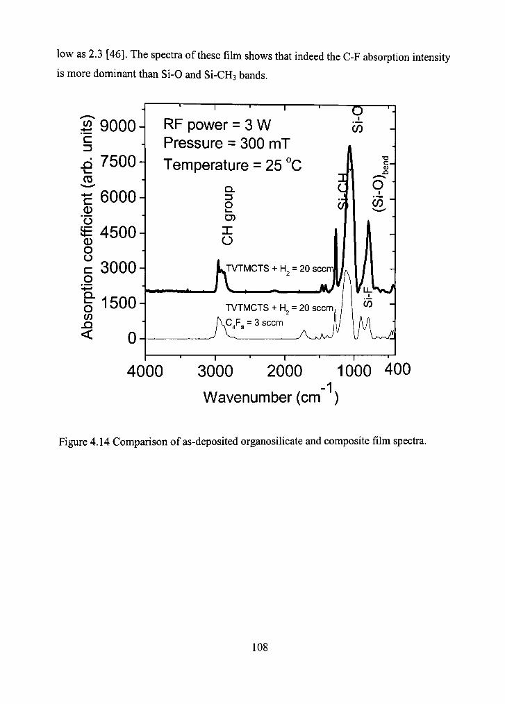
low as 2.3 [46]. The spectra of these film shows that indeed the C-F absorption intensity
is more dominant than Si-0 and Si-CH3 bands.
• 4 — '
"c
• 4 — '
c 0) o it= o o c o
o
<
9000-
7500-
6000-
4500-
3000-
1500-
0
RF power = 3 W Pressure = 300 mT
Temperature = 25 °C
i^<*dM
Q. 13 O D)
X
o
IT (y5
ki u
L T V T M C T S + H^ = 20 seem
TVTMCTS + H = 20 scorn
C F = 3 seem 4 o
CO
4000 3000 2000 1000 400 -1
Wavenumber (cm )
Figure 4.14 Comparison of as-deposited organosilicate and composite film specfra.
108

7000
S 6000 c n 5000-
^4000 _o
2-3000 (0
< 2000-1 •a -^ 1000-(0 E ^ 0
Pure TVTMCTS
with C F 4 8
1500 1350 1200 1050 900 750 -1
Wavenumber (cm ) Figure 4.15 Close-up of the normahzed Si-0 band of the organosihcate film and the
fluorinated organosilicate film.
The change in the FTIR spectra at 950 to 1250 cm"' range before and after SCCO2
freatment of film 2 is shown in Figure 4.16. The SCCO2 treatment of the film clearly
decreases the intensity of the band especially in the higher wavenumber side
corresponding to the C-F absorption band. Thus, we conclude that low molecular weight
C-F bonds dissolved in SCCO2. The dissolution of the C-F bonds is expected to create
molecular voids and/or nanopores in the matrix resuUing in the 10 to 14% decrease in k.
Furthermore, our studies establish that SCCO2 treatment is a very effective process to
reduce the dielectric constant of an organosilicate film. It is important to note that all the
films contain significant percent of highly cross-linked a-C:F bands after SCCO2
treatment and only low molecular weight C-F bands with low cross-link density are
dissolved.
109

E o
3500
3000-
-^ 2500-0) O
CD O O c o
2000-
1500-
& 1000 O CO
< 500-1
0-
As-deposited Pressurized
T T T T 1250 1200 1150 1100 1050 1000 950
Wavenumber (cm )
Figure 4.16 Changes in the absorption intensity of 950-1250 band after SCCO2 pressurization.
The SCCO2 treatment can be used successfully to reduce the dielectric constant of
PECVD deposited composite films. Low molecular weight species like CF or larger CO2-
soluble species containing CFx moieties can be extracted during the process. It is
hypothesized that the extraction creates molecular or nanoscale porosity thereby reducing
k. For example the k decreased from 2.87 to 2.48 with SCCO2 extraction at 200^.
Thermal annealing in N2 at 200°C of the film deposited with the same conditions showed
no change in k.
110

4.3 SCCO2 Porogen Extraction
SCCO2 treatment was used to create porosity in spin-on glasses. SCCO2 treatment
of organosilicate poly(methylsilsesquioxane) (PMSSQ) films was studied in this work.
This material has an inherently low k value, low moisture uptake, and excellent thermal
stability up to 500°C [165]. The k value can be further lowered by introducing
nanoporosity through the incorporation and subsequent thermal degradation of pore
generating organic materials, called porogens, into the PMSSQ matrix [166-168].
However, there are some inherent disadvantages in the thermal degradation process of the
porogen. The process window can be narrow, since the porogen decomposition must
occur below the glass fransition (To) of the thermally stable phase (when plasticized with
the porogen) so that the nanopores formed do not collapse. Since many organic polymers
have relatively low Tg compared to their degradation temperatures, this processing
consfraint can lead to incomplete porogen decomposition often resuhing in char
formation. To avoid these problems, supercritical carbon dioxide (SCCO2) treatment was
used to exfract C02-soluble porogens from the PMSSQ matrix at lower process
temperatures.
A solution containing appropriate quantities of a linear poly(propylene glycol)
(PPG) porogen, and low molecular weight PMSSQ dissolved in propylene glycol methyl
ether acetate (PM acetate) was prepared. The prepared solution was then filtered and
spun-coated on silicon substrates. The spun film was then heated briefly to 50°C on a hot
plate under nitrogen atmosphere to remove residual solvent before curing at 200°C to
produce the organic/inorganic polymer hybrid. This curing temperature is still well
below the thermal degradation temperature of the porogen in an inert atmosphere.
During matrix curing, phase separation of the porogen occurs via a nucleation and growth
process [169,170]. Thermal processing (baking/curing) was carried out under nitrogen as
this porogen decomposition begins as low as 150°C in the presence of frace amounts of
oxygen.
Porogen loading controls the pore sfi-ucture, open or closed, in the PMSSQ
matrix, hi this work, two porogen compositions in PMSSQ were stiidied: 0S75/25 and
111
OS45/55 (PMSSQ/porogen). The OS75/25 is expected to form nanohybrids with a
predominately dispersed porogen morphology while the OS45/55 resuhs in an
interconnected nanohybrid morphologies. For purely thermal processes, the final porous
morphology is dictated by that of the nanohybrid. In this section we will concentrate on
the resuhs for the OS45/55 sample.
Figure 4.17 shows the FTIR specfra of MSSQ, PPG, and MSSQ/PPG fihn. The
vibrational bands of MSSQ and PPG overlap; prominent among these are the OH stretch
at 3150-3700 cm"' and CHn stretch at 2800-3000 cm"'. For the CHn bands, the CH3
asymmetiic sfretch at 2960 cm"' is the only band observed in PMSSQ sample, whereas
the CH2 asymmetiic sfretch at 2915 cm"' is observed for PPG in addition to CH3 bands
corresponding to the symmetric and asymmetric stretch. Thus, in a hybrid film, all of the
CH2 contribution arises from PPG. A ratio of the area of this peak before and after
extraction gives a reasonable quantitative estimate of porogen remaining in the sample
after extraction.
The sfrongest vibrational bands for PMSSQ were observed at 1000-1200 cm"'.
From the Table 2.4 in Chapter II, the peaks at 1120 cm"' and 1030 cm"' in the as-spun
samples can be assigned to the cage and/or chains with non-bridging oxygen atoms and
network stiiictiires of MSSQ, respectively. In the FTIR spectra of PPG films, we also
observe the strongest peak in the region at 1000-1200 cm"'. This band is assigned as the
C-0 stretching vibration as observed for alcohols and ethers [124]. In the present work on
SCCO2 exfraction of PPG from PMSSQ matrix, we monitor the bands at 2800-3000 cm"'
as the indicator of the extraction process.
Using the static SCCO2 process (this experiment was done in the system described
in Figure 2.14 of Chapter II), the OS45/55 sample was pressurized at 7000 psi at 160°C
for 14 hours. The refractive index measurement of the as-spun sample was 1.442 ± 0.001,
this value decreased to 1.146 ± 0.001 after the SCCO2 treatment. This decrease in the
refractive index was attributed to the almost (8%) PPG was left in the pores) complete
removal of PPG from the films.
112

To verify the removal of PPG, FTIR measurement of the film before and after the
SCCO2 freatment is shown in Figure 4.18. In this figure, we can see that the peak at 2915
cm"' corresponding to PPG (CH2 asymmetric) decreased considerably. The reduction of
the CHn peak, especially the CH2 side, is a direct evidence of the PPG removal.
4.0 -
O 3.2 -O
n 2.4 H k. o (A
1.6 -
0.8 -
0.0 4000
i I X M S S Q + PPG
(cured @ 200 "C) « ? ^
PPG (baked @ 50°C)
M S S Q (baked @ 50°C)
3000 2000 -1 Wavenum ber (cm" )
1 0 0 0
Figure 4.17 FTIR spectra of MSSQ, PPG, and MSSQ/PPG films.
113

E1600-4 ^
.2 1200-o i t o 800-c 1 400-b. O M
5 0-
I I 1 AS-spun 0845/55 1 1 H S C C O j treated film
1 ' l | | Thermal extraction of PPG
2800 3200 3600 4000 -1
Wavenum ber (cm )
Figure 4.18 The effect of SCCO2 treatment on the CHn in the MSSQ/PPG hybrid fihn. Thermal extraction at 430°C of PPG is also shown.
Comparing the static SCCO2 extraction of PPG to the thermal decomposition is
also show in Figure 4.17. It can be noticed that static SCCO2 treatment, in addition to
taking long time (14 hours), it also does not remove PPG completely. In order to
overcome this problem, the new system shovm in Figure 2.15 of Chapter n was used in a
modified SCCO2 pulse mode. 5% of methanol was injected in the high-pressure vessel at
1500 psi and 150°C, then the pressure was ramped up to 7000 psi for the first pulse. A
similar procedure was used for the second and the third pulse. The system was left at
7000 psi and 150°C for 2 hours then depressurized to 1500psi for the first pulse. For the
second and the third pulse the system was left at 7000psi and 150°C for 30 minutes. The
system was flushed with pure SCCO2 5 times (pressurize and depressurize between 7000
and 1500 psi) to guarantee the removal of the methanol.
FTIR measurements of the films treated with the new method show a successful
extraction of PPG. Figure 4.19 shows a comparison of the two freatinents with the
114

thermal decomposition method. Even though the pulsed and methanol modified treatment
was done for a much shorter time, the exfraction process was better (only 4% PPG was
left in the pores) than the 14 hours static SCCO2 experiment. Refractive index
measurements are also consistent with the FTIR measurements. Due to the introduction
of pores after the PPG extraction, the refractive index decreased from 1.441 to 1.14. At
this point, our group is working on optimizing this process. By choosing the proper
solvent, pressure, and temperature, this process can be made more efficient.
1800
1600-
^ 1400-
I 1200
g 1000 "o £ 800
Q> O ^ 600-1
"S. 400 o w 200-1 <
0-1
•AS-spun OS45/55 Pulsed 3 hour
SCCOj treatment Static 14 hours
SCCOj treatment - Thermal decomposition
-200 2800 3000
Wavenumber(cm'^)
Figure 4.19 Comparison of the static, pulsed SCCO2, and thermal decomposition
treatments.
115

Since the volume fraction of the pores can be estimated from equation (2.92), then
the effective dielectric constant can also be estimated. Different models for the effective
dielectric constant of multi-component films have been developed. One of the first
models developed is the Maxwell-Gamett model, hi a tivo-component system, each
component is viewed as small spheres embedded uniformly in an ambient material with
an effective dielectiic constant ke [130, 131]. When the two-component film is placed in
an external electric field, the spheres get polarized and they develop local fields that can
be calculated from Clausius-Mossotti equation (equation 2.17). Given this description,
the Maxwell-Gamett equation is given by [130, 131]
k . + 2 k , + 2 F ( k . - k J
k ,+2k2-F(k , -k2)
where ke is effective dielectric constant, ki and k2 are the dialectic constants of the two
components, and V is the volume fraction.
If we consider equal-sized spheres, each sphere has a radius a, in a cubic matrix
with length (/). B. Sareni et al. [131] considered {a) and (/) to be dimensionless, and
studied the case for / = 2. Considering that a«l, then the spheres are isolated and they
only feel the external electric field. As Fis increased, the spheres start to experience the
local fields of each other. For the case a = 1, the threshold volume fraction for touching
spheres is F= 0.523 [131].
Figure 4.20 shows the expected values of the effective dielectric constant as a
function of the volume fraction of the pores for the methylselsisquioxane (MSSQ) films.
Maxwell-Gamett equation was used to calculate the effective dialectic constant for the
porous MSSQ films, for this case ki (MSSQ) = 3.1 and k2 (air) = 1. This calculation
assumes that porosity is the only reason for the reduction of the dielectric constant in the
MSSQ films.
Another method, which was developed on the same principles as the Maxwell-
Gamett equation, is the effective medium theory by Bmggemann [130, 131]. Similar
approach to the Maxwell-Gamett approach was used, and the volume fraction can be
calculated for different geometries of the pores. The two components of the film are
116
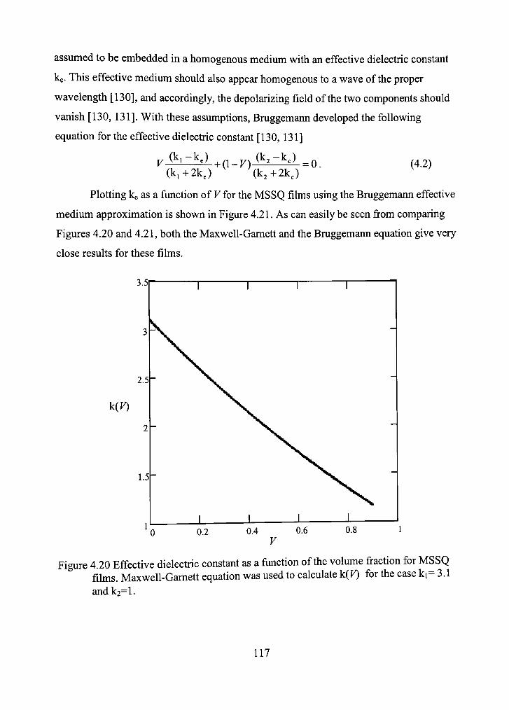
assumed to be embedded in a homogenous medium with an effective dielectric constant
ke. This effective medium should also appear homogenous to a wave of the proper
wavelength [130], and accordingly, the depolarizing field of the two components should
vanish [130, 131]. With these assumptions, Bmggemann developed the following
equation for the effective dielectiic constant [130, 131]
yiK-K) ^ ( i _ ^ ) ( k a - k e ) ^Q (4.2) ( k , + 2 k j ^ ' ( k , + 2 k j
Plotting ke as a function of V for the MSSQ films using the Bmggemarm effective
medium approximation is shown in Figure 4.21. As can easily be seen from comparing
Figures 4.20 and 4.21, both the Maxwell-Gamett and the Bmggemann equation give very
close results for these films.
k(F)
i.b
3
2.5
2
1.5
1 1
^ V
1 1
1 1
-
-
-
1 1 0.2 0.4 0.6 0.8
Figure 4.20 Effective dielectric constant as a fimction of the volume fraction for MSSQ films. Maxwell-Gamett equation was used to calculate k{V) for the case ki= 3.1 and k2=l.
117

k(V)
0 U.2 0.4 0.6 0.8 1
A V ^0.9,
Figure 4.21 Effective dielectric constant as a fimction of the volume fraction for MSSQ films. Bmggemarm equation was used to calculate k{V) for the case ki= 3.1 and k2=l.
The measured dielectric constant for the OS45/55 films after SCCO2 extraction
was 1.45. Using equation 2.92 the fraction of the pore volume was estimated to be 0.61.
Using Figures 4.20 and 4.21, the dielectric constant at this volume fraction is 1.72 and
1.66, respectively. These values are close to the measured value, but they are slightly
higher since there are other factors that contribute to lowering the dielectric constant. In
this case, the introduction of pores and the removal of OH were the main two factors, and
the models above consider only the porosity effect on k.
118

4.4 Hybrid Organosilicate Films Prepared by CVD
Since CVD is the main deposition technique used by the industry, it will be
advantageous to develop CVD hybrid films for the SCCO2 extraction experiment, hi
order to prepare hybrid films, Tetramethylsilane (TMS) was used as a host matrix for
poly(methylmethacrylate) (PMMA) polymer. Methylmethacrylate monomer was used as
the source for the PMMA component in the hybrid films.
Pure films of both materials were first prepared using our PECVD system. The
organosilicate film was prepared from 5% TMS and 95% N2O at 600 mTorr, 10 W at
room temperature. The FTIR measurements of organosilicate film show that this film
consists from Si-0 at 1037 cm"', Si-CH3 at 1268 cm"', and CHn at around 2950 cm"' [51,
124]. The PMMA film was prepared form 2.4-1 seem MMA at 5 W, 300 mTorr at room
temperature. FTIR measurements of the PMMA film show that the film consists of C=0
at 1729, CHn at around 2950 cm"', and C related peaks in the region 1020 to 1350 cm"'
[124]. The FTIR spectra of these films are shown in Figure 4.20. In this figure, we can
see that the CHn peak positions, and the Si-0 and C related peak positions in both
materials are overlapping. The C=0 peak is present only in the PMMA film. The change
in the intensity of this peak can easily be used to test the removal of the PMMA phase
from the hybrid film.
The hybrid film was deposited from 29 seem TMS, 20 seem N20,1 seem N2 +
MMA at 15 W, 600 mTorr at room temperature. The presence of C=0 peak at 1729 cm"
in the hybrid film FTIR spectmm (shown in Figure 4.22) shows considerable
incorporation of PMMA in the organosilicate film.
The refractive index measurements of the hybrid films are also in agreement with
the FTIR measurements. The refractive index was 1.448 ± 0.001 for the organosilicate
film, 1.504 ± 0.001 for the PMMA film, and 1.475 ± 0.001 for the hybrid fihn. The
refractive index value of the hybrid film indicates the existence of the two phases.
As a first attempt for the selective removal of the PMMA phase from the
organosilicate matrix, the hybrid films were treated using H2 plasma at 200°C. The resuh
of this treatment is also shown in Figure 4.22. It can be easily seen from this figure that
119

the C - 0 peak intensity decreased considerably after the H2 plasma treatment. This
indicates that the PMMA phase was selectively removed from the hybrid film.
(ti
c •
o c
o
<
0.70-0.35-0.00-
0.00--0.08--0.16-
0.08-0.00-
-0.08-
0.110-0.055-0.000-
TTVIStN^O
MMA vapor
{rMS + N,0 + (N+MMA)
H plasma freated on anode:
100 W, sod mTorr, aoCC
500 1000 1500 2000 2500 3000 3500 4000 450(
Wavenumber (cm" )
Figures 4.22 FTIR spectra of the organosilicate film, PMMA film, hybrid organosilicate/PMMA film, and the hybrid film after H2 plasma freatment.
Our fiiture goal is to optimize the PMMA loading into the hybrid film by
optimizing the deposition process. Controlling the PMMA loading confrols the pores
stmcture in the organosilicate matrix. Also we plan to use SCC02/co-solvent system to
selectively remove the PMMA phase from the organosilicate matrix. The SCCO2/CO-
solvent process needs to be optimized by choosing the proper co-solvent and processing
conditions.
120

CHAPTER V
SUPERCRITICAL CARBON DIOXIDE TREATMENTS OF
PLASMA-DAMAGED NANOPOROUS LOW-k Ffl MS
Plasma ashing, etching, and chemical cleaning can damage the dielectiic
properties of nonporous low-k films. Methylsilsesquioxane (MSQ) films were plasma
ashed and etched. FTIR measurements of these films shows that the plasma treatment
removes the hydrophobic methyl group (CHn) and it replaces it with the hydrophilic
silanol group (OH). Due to the high polarizability of the OH group [171-173], these films
atfract more moisture as they are exposed to ambient conditions. The loss of the CHn and
the increase of the OH concenfration increase the dielectric constant of these films.
SCC02/co-solvent system was used to remove the OH and recover the CHn
concenfration in these films. Due to the high diffiisivity, solvent power, and the absence
of the capillary force, SCCO2 can be used to treat pattemed dielectrics and it can easily
reach the damaged trenches and the vias that need to be treated.
Hexamethyldisiloxane (HMDSO) and hexamethyldisilazane (HMDS) were the
chemicals of choice for this freatment. In this chapter the detailed resuhs of the two
freatments will be compared.
5.1 SCC02/HMDS0 Treatment
The stmcture of the HMDSO molecule is shown in Figure 5.1. HMDSO reacts
with Si-OH and this produces Si-(CH3)3 group in these films.
121
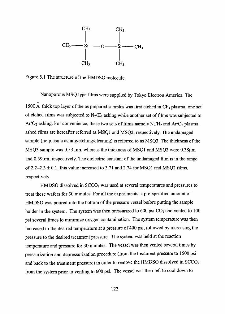
CH3 CH3
CH3 Si o Si CH3
CH3 CH3
Figure 5.1 The stmcture of the HMDSO molecule.
Nanoporous MSQ type films were supplied by Tokyo Electron America. The
1500 A thick top layer of the as prepared samples was first etched in CF4 plasma; one set
of etched films was subjected to N2/H2 ashing while another set of fihns was subjected to
Ar/02 ashing. For convenience, these two sets of films namely N2/H2 and Ar/02 plasma
ashed films are hereafter referred as MSQl and MSQ2, respectively. The undamaged
sample (no plasma ashing/etching/cleaning) is referred to as MSQ3. The thickness of the
MSQ3 sample was 0.53 fxm, whereas the thickness of MSQl and MSQ2 were 0.38^m
and 0.39|j.m, respectively. The dielectric constant of the undamaged film is in the range
of 2.2-2.3 ±0.1, this value increased to 3.71 and 2.74 for MSQl and MSQ2 fihns,
respectively.
HMDSO dissolved in SCCO2 was used at several temperatures and pressures to
freat these wafers for 30 minutes. For all the experiments, a pre-specified amount of
HMDSO was poured into the bottom of the pressure vessel before putting the sample
holder in the system. The system was then pressurized to 600 psi CO2 and vented to 100
psi several times to minimize oxygen contamination. The system temperature was then
increased to the desired temperature at a pressure of 400 psi, followed by increasing the
pressure to the desired treatment pressure. The system was held at the reaction
temperatiire and pressure for 30 minutes. The vessel was then vented several times by
pressurization and depressurization procedure (from the treatment pressure to 1500 psi
and back to the treatinent pressure) in order to remove the HMDSO dissolved in SCCO2
from the system prior to venting to 600 psi. The vessel was then left to cool down to
122

room temperature and finally it was vented to atmospheric pressure. The amount of
HDMSO added to the pressure vessel was such that HDMSO constituted 10 weight % of
the reaction mixture assuming the CO2 is an ideal gas. Table 5.1 presents the SCCO2
pressures and temperatures and the amounts of HDMSO used in each experiment. It is
noted that at the end of each experiment, there was generally about 1 cm^ HDMSO left in
the bottom of the reaction vessel; however, for the 200°C/9000 psi experiment,
approximately 5 cm^ was left in the vessel. The percentage of the added HMDSO was
reduced to 2% in attempt to avoid having any left over liquids, but that did not solve the
problem.
Table 5.1 The experimental conditions used for the SCCO2/HMDSO treatment. % HDMSO is based on freating CO2 as an ideal gas.
Temperature
(°C)
80
150
200
Pressure
(psi)
3000
9000
3000
9000
9000
9000
HDMSO Amount
(cm^)
3.0
9.0
2.5
1.5
7.5
7.0
% HDMSO
10
10
10
2
10
10
FTIR, thickness, refractive index, and the dielectiic constant of these films were
measured before and after each treatment. The FTIR absorbance spectrum of MSQ3
shown in Figure 5.2 reveals a strong peak at 1060 cm"' with a shoulder at 1140 cm"
corresponding to the Si-0 network and cage stmctiu-e vibrations. The absorption band
observed at 1250 cm"' and 840 cm"' are attributed to the CH3 symmetiic deformation
mode in (Si-CH3)n group and CH3 rocking vibration in Si-CH3 respectively. A peak at
2970cm"' corresponding to the asymmetric stretching vibration of CH3 is also observed.
123

We do not observe peaks with sufficient intensity either at 3200-3700 or at 930 cm"'
corresponding to the Si-OH vibrations in undamaged films.
The absorbance spectra of MSQl and MSQ2 are also shown in Figure 5.2. ft is
seen that the absorbance intensity of the CH3 band 2970cm"' decreased and the intensity
of the OH group (vibrational band at 3300-3750 cm"') increased as compared with
undamaged film (MSQ3). A small peak at 930 cm' is also observed in MSQl and MSQ2
indicating the increase in OH content. In case of N2/H2 ashed MSQl the hydrogen
radicals present in the plasma might have reacted with CH3 leaving the porous surface
more susceptible to moisture. As MSQ2 was Ar/02 ashed, oxygen plasma can easily
oxidize the methyl groups and form silanol groups as also observed by other research
groups [171-173]. This explains the increase in silanol concenfration and decrease in
methyl concenfration. The FTIR spectra in these two regions (CH band at 2800-3000
cm"' and OH band at 3200-3700 cm"') have been analyzed in detail by computing the
absorption coefficient after fitting the baseline. The procedure used for this purpose has
been described earlier in Chapter n. The insets in Figure 5.2 show the CH and OH
regions of the specfra.
124

w 'E
3^ o u c (0 .a o 0)
MSQl MSQ2 MSQ3
MSQ3 MSQl
- 2 . 2 0 - | M S Q 2
-2.25 4000 3000 2000
Wavenumber (cm' )
1000
Figure 5.2 The FTIR spectra of the samples in the as-received state. MSQl and the MSQ2 are the plasma-treated films, while MSQ3 is the film without any treatment. The insets show the CH3 and OH bands of these films.
The results of the refractive index measurements conducted on these films are
summarized in Table 5.2 below. The MSQ samples initially (as-received) had refractive
indices of 1.26, 1.31, and 1.31 for samples MAQ3, MSQ2, and MSQl, respectively
125
Table 5.2 Refractive index measurements for the MSQ samples treated at different temperatures and different pressures.
Sample
MSQl
MSQ2
MSQ3
Refractive Index
Temperature (°C)
80
150
200
As received
Temperature (°C)
80
150
200
As received
Temperature (°C)
80
150
200
As received
Pressure (psi)
3000
1.302 + 0.008
1.30310.001
9000
1.32510.001
1.330 ±0.004
1.292 ±0.001
As-received
(1.317 ±0.002)
Pressure (psi)
3000
1.314 ±0.004
1.314 ±0.004
9000
1.312 ±0.002
1.310 ±0.006
1.293 ±0.009
As-received
(1.317 ±0.008)
Pressure (psi)
3000
1.263 ±0.003
1.273 ±0.004
9000
1.278 ±0.001
1.270± 0.007
1.284 ±0.003
As-received
(1.261 ±0.004)
As well be shown subsequently, the FTIR resuhs show a 30% decrease in the CH
concentration and a nine-fold increase in the OH concenfration for the MSQl sample
compared with MSQ3. Similarly, a 40% decrease in the CH concenfration and a six-fold
increase in OH concentration for the MSQ2 sample relative to MSQ3 sample. As
126

mentioned earlier, the surfaces of MSQl and MSQ2 samples became rough due to ashing
and cleaning processes performed on the samples before we received them, ft seems that
considerable damage was done to these samples due to harsh ashing and cleaning
treatments.
The FTIR results are shown in Figures 5.3 through 5.7. Figure 5.3 shows the
FTIR specfra of the as-received and after SCCO2/HMDSO treated MSQl sample. This
figure shows an increase in CH bands at 2900 cm"' and a decrease in the OH bands at
3500 cm"' after the treatment. This can be seen more clearly in Figures 5.4 and 5.5 for
MSQl samples pressurized at various temperatures and 9000 psi.
Figures 5.6 and 5.7 more explicitly show the effect of treatment temperature on
the concenfration of CH and OH concenfration for HMDSO treatment at 9000 psi for all
of the MSQ samples. CH concentration reached a maximum at 150°C for MSQl and
MSQ2 samples. The CH concentration decreased at 200°C for these samples. For MSQ3
samples, there was no change in CH concentration when the temperature and pressure
were changed.
The increase in CH concentration for the treated MSQ samples at 3000psi and
9000psi was the same for all samples at each temperature even though the concentration
of HMDSO dissolved in SCCO2 and the solubility of SCCO2 in the film is expected to be
higher at 9000 psi. It is interesting to note that the CH concentration was also unchanged
when the HMDSO concentration was reduced from 10 % to 2% (both percentages based
on CO2 as an ideal gas).
127
0.3
0.2-1
O c ra £ 0.1 o (A ^
0.0
-0.1 -
•As-received MSQ1 MSQ1 pressurized at 9000 psi 150°C im 10% HMDSO for 30 min.
E o
o
4000 3000 2000 1000 Wavenumber (cm")
Figure 5.3 IR absorbance specfra for (a) As-received MSQl and (b) MSQl pressurized at 9000 psi and 150°C in 10% HMDSO for 30 minutes.
400 -
E 3. 300 c 0)
'JS I 200 O c .0 "§• 1 0 0 o </) ^
0 -
3100
Sample: MSQ1 as-received 9000 psi and SO'C 9000psi and 150°C 9000psi and 200°C
3000 2900 Wavenumber (cm'^)
2800 2700
Figure 5.4 IR absorption specfra of CH groups after pressurization at different
temperatures.
128
2 5 0
-.. 2 0 0 -
0) 'o E O 1 0 0 -c o
1 8 50H ^
0 -
S a m p i e : M S Q l a 8 - r e c e i v e d SOOOpsI, 80°C SOOOpsI, 1 50°C 9 0 0 0 p s l , 2 0 0 ° C
4000 3800 3600 3400 3200 Wavenumber (cm'')
3000
Figure 5.5 ER absorption spectra of OH group after pressurization at different temperatures.
5 0 0 0 0
iS 'E 3 .g 4 0 0 0 0 -IS
•a c o
•a 3 0 0 0 0 X
o "S c ~ 2 0 0 0 0 -s c 8 c O 1 0 0 0 0 -
M S Q l M S Q 2 M S Q 3
( a s - r e c e i v e d film )
5 0 1 0 0 1 5 0
T e r n p e r a t u re (°C )
2 0 0
Figure 5.6 Effect of pressurization and temperatiire on CH concenfration in MSQ samples.
129

c 3
•e 45. c o
.Q X O •8 c o I 8 c o u
1 0 0 0 0 0 -
8 0 0 0 0 -
6 0 0 0 0 -
4 0 0 0 0 -
2 0 0 0 0 -
T
"~ ——.
(as-received film)
*. 1 ' 1
-k
~ - * — —
1 —J
^ k
~""-~*-
1 1
^ •
- M S Q 2 MSQ3
f
1 50 100 150
Tern perature (°C) 200
Figure 5.7 Effect of pressurization and temperatiire on OH concentration in MSQ samples.
Several factors can affect the CH incorporation and OH removal processes: (1)
solubihty of HMDSO in SCCO2, (2) solubihty of SCCO2/HMDSO in the fihn, (3)
diffiisivity of HMDSO and H2O in the film, and (4) chemical reaction rate. As
mentioned earlier, increasing the pressure did not significantly affect CH and OH
concentrations, whereas temperature did. At higher temperatures, the solubility of
SCCO2/HMDSO in the film and in SCCO2 is expected to be reduced, whereas diffiisivity
and chemical reaction rate should increase. As seen in Figures 5.4 and 5.5, increase in
CH concentration occurs along side with OH removal at 80°C and 150°C. At 200°C,
concentrations of OH and CH both decrease. The MSQl and MSQ2 samples treated at
200°C showed the best results with considerable incorporation of CH and removal of OH,
accompanied by a decrease in the refractive index. This clearly shows that the dielectiic
properties of the nanoporous organosilicate films damaged by ashing/cleaning processes
can be improved significantly by SCCO2/HMDSO treatinent. The dielectric constant for
these films was calculated from the CV measurements and the results are shown in Table
5.3 below. A metal/insulator/silicon stmcture was consti-ucted by depositing Ti elecfrodes
130

on these films. The maximum capacitance was obtained from the accumulation region of
the CV curves measured for these samples, and it was used to calculate the dielectric
constant of the SCCO2/HMDSO treated films.
Table 5.3 The dielectric constant values for MSQl sample after different treatments. All the dielectric constant measurements were done three months after SCCO2/ HMDSO treatments.
Sample
Number
1
2
3
4
Sample Details
As-received
First annealed in N2 at 200°C for
four hours and then pressurized
3122 psi, 158°C for 30 minutes
with 10% HMDSO
As given annealed at 400°C for
one hour in N2
Sample 2 annealed at 400°C for
one hour in N2
Dielectric constant ±10%
MSQl
3.71
3.43
2.27
2.34
The thermal stability of this treatment was evaluated by annealing the treated
samples at 400°C for 1 hour in N2. Figure 5.8 shows the FTIR absorbance spectra of
MSQl sample (a) as-received, (b) SCCO2/HMDSO treated and (c) treated sample after
400°C annealing.
Figure 5.9 shows that significant amounts of CH incorporated in the film with
SCCO2/HMDSO treatment have been removed after annealing at 400°C. The
concentration of CH groups reduced to almost the same level as in the as-received sample
after 400°C annealing. The concentration of OH groups decreased after treatment
compared to the as-received MSQl when the FTIR was measured immediately after
131

freatment as seen in Figure 5.10. However when FTIR absorbance was measured after
exposing the HMDSO treated sample to laboratory ambient for a bout 3 months, the
concenfration of OH bonds increased significantly and it was close to the value for the as-
received sample as seen in Figure 5.11. These observations indicate that even though the
SCCO2/HMDSO treatment can recover the methyl group concenfration, this treatment is
thermally unstable. The removal of the incorporated methyl group after the 400°C
annealing renders this treatment as not suitable to cure the plasma-damaged samples.
0.35
0.30-
^^ 0.25 -o ^ 0.20 -c •5 0.15-E § 0.10-o I 0.05-
S- 0.00 -o « .9 -0.05 -<
-0.10-
-0.15-
(a) as received MSQ1 (b) annealed in N at 200°C and treated with SCCO /HMDSO
(c) sample (b) annealed in N at 400°C for one liour
T T T 500 1000 1500 2000 2500 3000 3500 4000 4500
Wavenumber (cm" )
Figure 5.8 FTIR absorbance spectra of the (a) as-received, (b) SCCO2/HMDSO freated and (c) SCCO2/HMDSO treated + annealed MSQl sample.
132
E
c 0)
'o E a> o O
o w <
550 -r
500-
450 -
400 -
350 -
300 -
250-
200-
150 -
100-
50-
0-
-50
-as-received MSQ1 sample 200°C annealed In N, and then SCC0,/HMDS0 treated at 3000 psi, 155°C
-Treated sample annealed at 400'C In N, for one hour
2700 2750 1
2800 2850 1 • 1 ' 1 ' 1
2900 2950 3000 3050 3100 3150
Wavenumber (cm' )
Figure 5.9 Concentration of CH bonds in (a) as-received (b) SCCO2/HMDSO freated and (c) treated + 400°C annealed samples.
4 0 0
350 -
„ 300 c 01
u 2 50 -!c ?! O 2 0 0 -c o = 150 H O
<
50 -
0 -
30
• a s - r e c e i v e d M S Q l s a m p l e S C C O , / H M D S O t r e a t e d s a m p l e
T r e a t e d + a n n e a l e d a t 4 0 0 ° C
00 3 2 0 0 3 4 0 0 3 6 0 0 3 8 0 0 W a v e n u m b e r (cm'^)
4 0 0 0
Figure 5.10 Concentration of OH bonds in (a) as-received (b) SCCO2/HMDSO treated and (c) treated + 400°C annealed MSQl samples.
133

400
^ ~ 350 -
•^ 300 H c « "o 250 -
O 200 - I c o •*: 150 -& o ^ 100 -I <
50 -
0 -
30
MSQ1 •FTIR measured Immediately after SCCO^/HMDSO treatment measured three months after treatment.
00 3200 3400 3600 3800
W a v e n u m b e r (cm'^)
— I — 4000
Figure 5.11 Increased absorption of moisture with time after treatment in case of SCCO2/HMDSO freated MSQl sample.
5.2 SCCO2/HMDS Treatment
Hexamethyldisilazane (HMDS) has been used by different research groups as a
potential method to cure the damaged films [171-173]. HMDS reacts with silanol groups
forming (CH3)3-Si-O-Si-. Some groups [173] used spin-on method to deposit a layer of
HMDS on the damaged porous films and then subjected the films to hot plate baking at
different temperatures other groups [171, 172] have treated the plasma damaged films in
HMDS vapor by exposing the damaged films to HMDS vapor at different temperatures.
We believe that these treatinent methods are effective in replacing the silanol groups with
methyl groups on the surface of the film only and not in the bulk of the film. It is
proposed that HMDS dissolved in supercritical carbon dioxide (SCCO2) can be more
effective in curing the plasma-damaged films; both on the surface and in the bulk.
134

The stmcture of the HMDS molecule is shown in Figure 5.12 below. As in the
case of the HMDSO freatment, the HMDS will react with Si-OH to produce (CH3)3 -Si-
O-Si-.
CH3
CH3 H CH
Si N Si CH,
CH3 CH
Figure 5.12 The stiiicture of the HMDS molecule.
SCCO2/HMDS treatment was performed at different temperatures as given in
Table 5.4. The HMDS treated films were also armealed at 400°C for one hour in vacuum
to study their thermal stability. These films were also treated with HMDS vapors for 30
minutes at 150°C for comparison with SCCO2/HMDS treatment. The FTIR spectra of the
plasma-damage and the undamaged film were shown earlier in Figure 5.2.
Table 5.4 Experimental conditions for the SCCO2/HMDS treatment.
Sample
No
1
2
3
4
5
Solvent
used
HMDS
HMDS
HMDS
HMDS
HMDS
Treatment
temperature
CO 55
80
125
150
200
Pressure
(psi)
3000
3000
3000
3000
3000
Weight % of the
solvent used
2
2
2
2
2
135

The FTIR absorbance measurements of SCCO2/HMDS treated MSQl samples at
different temperatures show that the OH groups (vibrational band at 3300-3750 cm"')
have been removed considerably while there is significant incorporation of methyl group
following the freatment with HMDS and the subsequent silylation reaction as follows
[172].
(CH3)3Si-NH-Si(CH3)3+ HO-Si =(s) ^ (CH3)3-Si - O - Si =(s) + (CH3)3 - SiNH2(g) (5.1)
(CH3)3 - SiNH2(g) + HO-Si =(s) ^ (CH3)3— Si — O — Si =(s) + NH3(g) (5.2)
Detailed analysis of CH3 vibrational band has been showTi in Figure 5.13 This
clearly shows that the intensity of the band at 2970cm"' corresponding to the asymmetric
vibrational band of CH3 increases after SCCO2/HMDS treatment. The CH3 peak slightly
shifts towards the lower wave number by 5cm"' as seen in Figure 5.14. The full width at
half maximum (FWHM) of this peak increases after SCCO2/HMDS treatment and it is
almost independent of the treatment temperature within the errors of fittings. In the as-
given film, we expect only one CH3 group to be bonded to each Si atom in a
methylsilsesquioxane (MSQ) type film. Since three methyl groups (CH3)3 are attached to
each Si atom after treatment with SCCO2/HMDS, the environment surrounding the Si
atom in the film changes and the change in the peak position may be attributed to this
change in the environment. Furthermore, the areas have been computed for this peak in
order to calculate the concentration of CH3 bonds and a plot of CH3 concentration with
treatment temperature is shown in Figure 5.15. It is seen that significant amounts of CH3
groups have been incorporated in the film even at a low process temperatiu-e of 55°C.
This is significant considering the fact that HMDS has a boiling point of 125°C. This is
possibly due to the solubility of HMDS in SCCO2 even at 55°C. ft is seen that the amount
of CH3 groups incorporated increases linearly with an increase in the treatment
temperature. This increase may be due to the formation of a thin solid layer on the
136

surface. The increase in the thickness of this layer with increasing the treatment
temperature was not included in the FTIR analysis of the samples and could be the reason
for the observed increase in the CH3 concentration. For comparison, films were subjected
to HMDS vapor freatment at 150°C. The amount of CH3 incorporated with vapor
treatment shovm in Figure 5.15 is correspondingly lower than that with SCCO2/HMDS
freatment. As SCCO2 does not suffer from any capillary forces, SCCO2 is likely to carry
HMDS more efficiently into the bulk of the film. This explains the lower concentration of
methyl groups in vapor treated film. Therefore, SCCO2/HMDS treatment is a more
effective technique to cure the damage caused by plasma ash/clean/heat. The trend is
similar for SCCO2/HMDS treated MSQ2 samples.
400-
r 300 0)
% 200 o o
I 100 o (/>
^ 0-
55"C 80°C 125°C 150°C 200"C
as-received MSQ1
^ata
3100 3000 2900 Wavenumber (cm" )
2800
Figure 5.13 The increase in the CH3 concentration as a fimction of SCCO2/HMDS freatment temperature.
137

50 100 150 T r e a t m e n t Tern p e r a t u r e ( °C)
2980
- 2 9 7 8
- 2 9 7 6 E o
- 2 9 7 4 Q.
ra 0) Q.
- 2 9 7 2
2970
Figure 5.14 Shift in the peak position and peak width after HMDS freatment of MSQl samples at different temperatures.
W 18000-1 c 5 16000-1
O 'Jo'14000-
O C C 3 12000-
o n 2 >2.ioooo c g 8000 c o o
MSQl MSQ3 Treated & Annealed MSQl Vapor treated MSQl
i i
As-g iven M S Q 3
As-g iven IVISQI
— - t reated and annea led IVISQI
vapor t reated M S Q l
50 100 150 200
Temperature (°C) 2 5 0
Figure 5.15 Effect of SCCO2/HMDS treatment temperatiires on the concenfration of CH3 bonds.
138

Figure 5.16 and Figure 5.17 show the absorption band for the OH group and its
concenfration dependence on the freatment temperature respectively. It is seen that
though the OH concentration has decreased significantly, it has not been completely
removed from the plasma-damaged films after SCCO2/HMDS treatment. In fact,
approximately 45% of OH concentration still remained in the film with respect to the
initial level in the damaged MSQl film.
600
£500-1 o
= 400-] O
gsoo o 0200-I
S 100-1 <
0-1
As-received MSQl 55°C 80°C 125°C 150°C 200°C As-received MSQ3
4000 3800 3600 3400 3200 3000 -1
Wavenumber (cm )
Figure 5.16 A plot of the absorption intensity in the OH region of the spectioim for MSQl samples treated at different temperatures.
139

(A •a c o
Si
210000-
180000
150000
O ^ gl20000-| 3
•"S Is 90000-^
o u c o o
60000
30000-]
• MSQ1 • MSQ3 ^ treated & annealed at 400°C o Vapor treated MSQl
As-given f MSQl
As-given MSQ3
^ HMDS Vapor
treated
treated and
anriealed at 400°C mc
— I —
50 100 150 200 250
Temperature ( C) Figure 5.17 Dependence of the concentration of OH bonds removed on the fi-eatment
temperature.
The possible explanation for the incomplete removal of OH groups is as follows.
It is clear from equations (5.1) and (5.2) that each OH group has been replaced by three
methyl groups. When a smaller group (OH) is replaced by a bigger group such as three
methyl groups as in this case, it shields the neighboring OH group attached to the
neighboring silicon from undergoing similar reaction with HMDS. This prevents the
removal of the OH group from the neighboring silicon atom. This is called the steric
hindrance effect [51] and it is shown in Figure 5.18 below. Thus, it is quite likely that the
present treatment would not be able to completely remove OH groups. A high
temperature annealing typically at 400°C for a few hours followed immediately by
HMDS/SCCO2 treatment would be a possible way to remove OH groups completely.
140
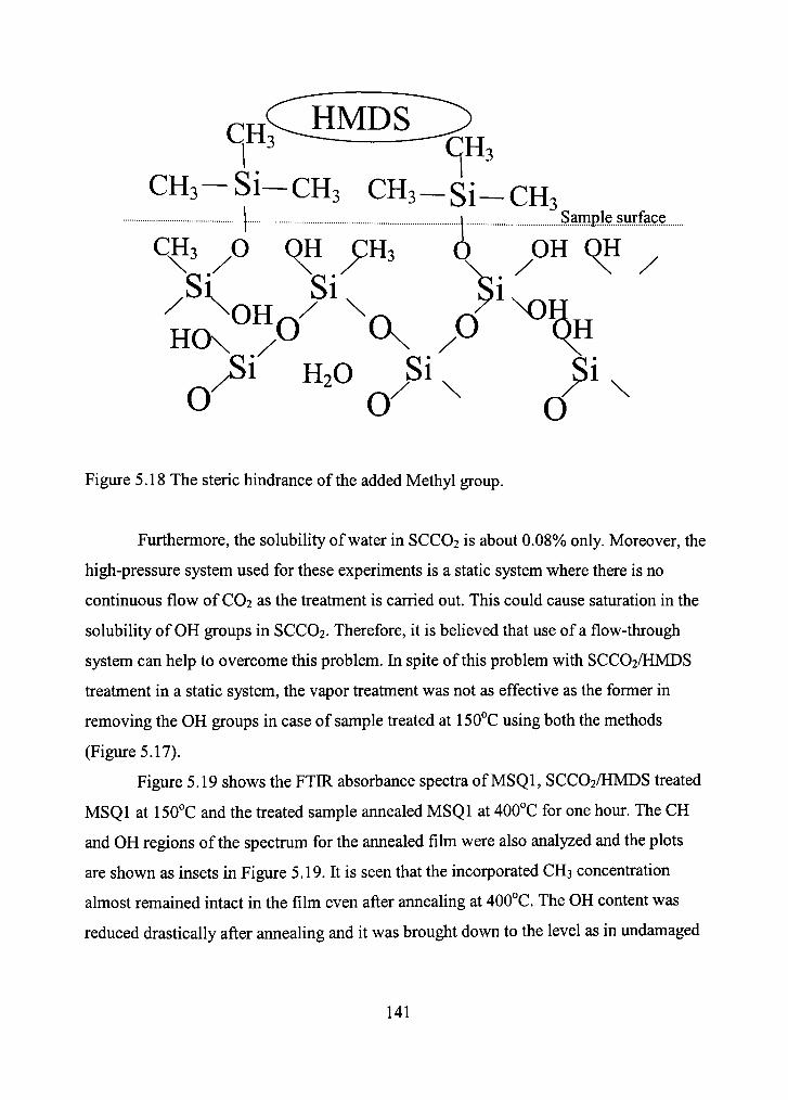
( . j j^ HMDS CjH;
CH3-Si-CH3 CH3-Si-CH3 Sample surface
CH3 O QH CH3 5 OH QH
/Si, S i , $i (
0> "=%/'x / x
Figure 5.18 The steric hindrance of the added Methyl group.
Furthermore, the solubility of water in SCCO2 is about 0.08% only. Moreover, the
high-pressure system used for these experiments is a static system where there is no
continuous flow of CO2 as the treatment is carried out. This could cause saturation in the
solubility of OH groups in SCCO2. Therefore, it is believed that use of a flow-through
system can help to overcome this problem. In spite of this problem with SCCO2/HMDS
treatment in a static system, the vapor treatment was not as effective as the former in
removing the OH groups in case of sample treated at 150°C using both the methods
(Figure 5.17).
Figure 5.19 shows the FTIR absorbance spectra of MSQl, SCCO2/HMDS freated
MSQl at 150°C and the treated sample annealed MSQl at 400°C for one hour. The CH
and OH regions of the spectmm for the armealed film were also analyzed and the plots
are shown as insets in Figure 5.19. It is seen that the incorporated CH3 concenfration
almost remained intact in the film even after annealing at 400°C. The OH content was
reduced drastically after annealing and it was brought down to the level as in undamaged
141

MSQ3. A similar trend was also observed in MSQ2. These observations indicate that the
SCCO2/HMDS treated samples are thermally stable up to 400°C (compare to
SCCO2/HMDSO treatment). Moreover, the treatment can be performed at much reduced
temperature as low as 55°C. The amount of CH3 incorporated with SCCO2/HMDS is
significantly higher than with HMDS vapor treatment at the corresponding temperature.
The dielectric constant for these films was measured in the same way as the in the
SCCO2/HMDSO case. A metal/insulator/Si stmcture was used to perform CV
measurements on these films. The maximum capacitance was found from the
accumulation region of these curves, and this value was used to calculate the k value for
these films before and after treatment. Table 5.5 shows a comparison of the dielectric
constant of the films before and after treatment. The dielectric constant of the as-received
MSQl sample is high and it is 3.71 (as was mentioned earher) because of the lower
concenfration of hydrophobic methyl groups and higher concenfration of hydrophilic
silanol groups. With the SCCO2/HMDS treatment at 150°C for 30 minutes, the dielectric
constant is brought back to 2.49 due to the replacement of silanol groups with methyl
groups. Furthermore, upon annealing the treated film at 400°C, the dielectric constant is
further reduced to 2.30. Since, the OH group concentration is lowered even more after
annealing the treated sample at 400°C, then we expect a lower k value for this sample, h
is to be mentioned here that the error in the measurements of k values is about ± 0.1. In
case of MSQ2, the measured k values of as-received MSQ2, SCCO2/HMDS freated
MSQ2 at 150°C, and SCCO2/HMDS treated at 150°C then annealed at 400°C MSQ2
sample are 2.74, 2.41 and 2.29, respectively. The k value of HMDS vapor treated MSQl
film is 2.82 and is higher than the SCCO2/HMDS treated sample at the same temperature.
The reason for the higher value in the k value of the vapor treated sample is the lower
CH3 group concenfration and the higher OH groups concentration in the vapor freated
film as shown in Figures 5.15 and 5.17.
142

-1.7
a> u c re
O tn
• 1 . 8 -
• 1 . 9 -
- 2 . 0 -
-2 .1
5. 450
I J 300
.S 150
0
31 SO 3000 2850 2700 Wavenumber (cm')
4000 3200 2400 1 6 0 0 - i i Wavenumber (cm' )
800
Figure 5.19 FTIR absorbance specfra of (a) plasma damaged MSQl, (b) SCCO2/HMDS freated MSQl at 150°C for 30 minutes and (c) Treated MSQl sample annealed at 400°C for one hour. Insets show the CH and OH regions of the specfra.
It is worth mentioning here that the CH3 concentration did not change with
SCCO2 and HMDS treatment in MSQ3 (undamaged) films as expected. The dielectric
constant measured for the treated and then annealed MSQ3 sample at 400°C is 2.30. Thus
it is evident that SCCO2/HMDS treatment cures the plasma damaged MSQl films more
effectively than the vapor freatment.
143

Table 5.5 Dielectric constant measurements of the SCCO2/HMDS treated MSQl sample.
Sample
#
1.
2.
3.
4
5
Sample description
As-received MSQl
SCCO2 +HMDS at 150°C, 3000psi MSQl
for 30 minutes
SCCO2 + 2% HMDS treated MSQl at
150°C, 3000psi for 30 minutes and then
annealed 400°C for one hour
HMDS vapor treated MSQl at 150°C
SCCO2 + 2% HMDS treated MSQ3 at
150°C, 3000psi for 30 minutes and then
annealed 400°C film for one hour
k value
±0.1
3.71
2.49
2.46
2.82
2.30
Both SCCO2/HMDSO and SCCO2/HMDS treatments of the plasma-damaged
films were able to increase the CH3 concentration, and both treatments were able to lower
the OH concentration. Annealing the treated fihns at 400°C indicates that the
SCCO2/HMDS is more thermally stable than the SCCO2/HMDSO freatment. This might
be explained as follows, the HMDSO does not really interact with Si-OH as we
previously thought, but instead a layer of HMDSO is deposited on the fihn surface. This
HMDSO layer gives rise to the increase in the CH3 concentration observed in the FTIR
measurements. The decrease in the OH concenfration in this case is due to annealing
effects only. In the case of the HMDS treatment, the Si-N bond breaks and this allows the
formation of the (CH3)3 -Si-O-Si-, this reaction of the HMDS with Si-OH (see equations
144
(5.1) and (5.2)) does add the methyl group the MSQ film, and this is what make the
SCCO2/HMDS freatment thermally stable.
5.3 Contact Angle Measurements of SCCO2/HMDS Treated MSQ Fihns
A set of nanoporous MSQ films was provided by Tokyo Elecfron America. These
samples were plasma etched. The thickness of these samples decreased from about 1 im
for the as-spun film to about 0.9 -0.95|am for the etched film. Due to plasma-etching the
removal of some of the CHn from the film will reduce the hydrophobicity of the film. In
order to recover the CHn content, the film was treated using SCCO2/HMDS at 80°C and
3000 psi. The freatment time was changed from 1 to 30 minutes.
Since there was no significant damage to the film due to plasma etching, FTIR
measurement was unable to detect any changes in the film stmcture before and after
SCCO2/HMDS treatment. Since the film's nature changes from hydrophobic to
hydrophilic after the removal of CHn, then contact angle measurement can be a direct
measure of the recovery of the hydrophobicity, and hence CHn. Figure 5.20 shows the
effect of the SCCO2/HMDS treatment on the contact angle of the film. This figure shows
that even the 1 minute treatment was able to recover the film hydrophobicity to the value
of the undamaged film. This experiment is a further proof that the SCCO2/HMDS
treatment is an effective method for plasma-damage recovery.
145

•
—» 100-0) 0)
£ 0) 80-o
0) D) S 60-< U ra S 40-o o
20 -
Sample without etching
I I
I 0
11
Etched MSQ sample 1 . , . , 1 1 1
5 10 15 20
•
1 ' 1 25 30
Treatment Time (min.)
Figure 5.20 Contact angle measurements as a function of the treatment time for the new nanoporous MSQ samples.
146

CHAPTER VI
CONCLUSION
hi this dissertation, the use of PECVD and SCCO2 were discussed as methods to
prepare low k films. Introduction of nanoporosity was the main approach adapted to
lower the dielectric constant. SCCO2 was also used to recover the dielectric properties of
plasma-damaged nanoporous low k films.
6.1 Triple-Phase a-SiC:H/SiO/C:H Films
Triple-phase (or tiiple-component) a-SiC:H/SiO/C:H films were deposited using
PECVD from the a liquid source (diethylsilane). Changing the flow rate of the liquid
source changes the Si concentration in the films. Increasing the flow rate of diethylsilane
increases the Si concenfration in the film and this leads to the lowering of CHn
concentration. The deposition power has a direct effect on the Si and CHn concenfration
in the fihns. Higher power fragments diethylsilane molecules, which increases the Si
concenfration. In general, the increase of the Si concentration increases the dielectiic
constant of the as-deposited films. Higher power also helps to prepare films with better
crosslinking.
Treating these films with SCCO2 at 200°C removed CHn more efficiently than
annealing the films at the same temperature. Addition of a co-solvent to SCCO2 is
expected to remove low molecular weight CHn groups completely.
The removal of CHn is believed to introduce nanopores in the films. SEM
measurement of these films was unable to detect any pores or features that resemble
them. This implies that the pore size is beyond the SEM resolution, which leads us to
believe that these pores are of nanometer size.
Dielectric constant measurement of these films shows that annealing the films at
450°C reduced the dielectric constant values from about 4.23 to 2.1.
147

6.2 Organosilicate and Fluorinated Organosilicate Films
Deposited from TVTMCTS
A new source, TVTMCTS, was used in a PECVD process to deposit low-k
organosilicate films. The TVTMCTS molecule has a ring stmctiire that can help to
introduce free space in the film. The power used to deposit these films was set to the
lowest possible value, and the pressure of the chamber was set to highest possible value.
This was a necessary step to reduce TVTMCTS fragmentation and to lower the energy of
ion bombardment of the deposited film, which helps to preserve the ring stmcture of the
TVTMCTS molecule. Dielectric constant values as low as 2.65 were obtained for the
films deposited at 3 W. These films showed also good thermal stability for annealing
temperatures up to 400°C.
Fluorocarbon films were deposited from C4F8, the solubility of these films in
SCCO2 was tested by pressurizing the films at 200°C at 8650psi for 8 hours. These films
were dissolved completely after this treatment. In an attempt to exploit the solvent power
of SCCO2, mixtures of TVTMCTS and C4F8 were used to deposit fluorinated
organosilicate films. A subsequent treatment with SCCO2 was used to selectively remove
the fluorocarbon phase. The removal of the fluorocarbon phase infroduces more free
space to the fihn and this lower the dielectric constant even more. Our experiments show
that the SCCO2 treatment has no effect on the pure organosilicate films (TVTMCTS
films), but this treatment partially removed the fluorocarbon from the fluorinated
organosilicate film. The removal of the fluorocarbon did reduce the dielectric constant of
these films to values as low as 2.48. Moreover, the addition of the fluorine damaged the
ring stiiicture of the TVTMCTS molecule as the FTIR measurements indicates. The
fluorine species in the plasma reacts with Si atoms and forms SiF, during this process the
ring stmcture is damaged and the benefits of using TVTMCTS are lost.
Using SCCO2 freatment in pulse mode and adding a modifying co-solvent is an
efficient method for selective extraction. Pulsed SCC02/Methanol was used successfiilly
to remove PPG from hybrid MSSQ/PPG films. This treatment decreased the process time
considerably and was more efficient in removing PPG than the static SCCO2 freatinent.
148

6.3 SCC02 Treatment of Plasma-Damaged Porous Low-k Films
Due to the attractive physical properties of SCCO2, it was used as a carrier for
HMDSO and HMDS to freat plasma-damaged porous low k films. The SCCO2/HMDSO
freatment does recover the methyl group concentration, but this treatment tiimed out to be
thermally unstable after 400°C annealing. SCCO2/HMDS treatment was used as an
altemative for the previous treatment. This treatment was successful in recovering the
methyl group concentration and lowering the silanol concenfration. The SCCO2/HMDS
freatinent was also thermally stable up to 400°C. The incomplete removal of the silanol
group can be attributed to the steric hindrance [51] of the added methyl group. The added
methyl group forms "a barrier" on the surface that prevents the HMDS from reaching and
reacting with the underlying silanol molecules. The advantage of using SCCO2/HMDS
treatment over the direct use of HMDS [167, 168] resides in the fact that SCCO2 has a
gas like diffusivity and it does not suffer from capillary forces due to its low viscosity.
Due to these factors, SCCO2/HMDS treatment can be used successfully to treat pattemed
dielectrics, and it can easily get into pores, trenches and vias to treat them. Dielectric
constant measurements of the plasma-damaged films show a recovery of the dielectric
constant value. The k values decreased from 3.71 for the damaged fihn to 2.3 for the
same film after SCCO2/HMDS treatment. This k value of the cured film is equal to the k
value of the undamaged film.
6.4 Future Work
Pulsed SCC02/co-solvent treatment needs to be optimized. The process
temperature and pressure need to be optimized to the lowest possible values to make the
process more practical for industry. New hybrid films need to be developed for these
experiments. The new films can be either CVD deposited or spin-coated films. The
important criterion for these films is that the main matrix should be SCCO2 insoluble.
The pulse mode confrols need to be changed from manual to computer control,
where a better confrol can be achieved for the pressurization/ depressurization process.
149
REFERENCES
I] The hitemational Technology Roadmap for Semiconductors (ITRS), 2001.
2] J.Simpson, A. St. Clair, Thin Solid Films, 308-309,480 (1997).
3] J. Golden, C. Hawker, P. Ho, Semiconductor hitemational, 24, 79, May (2001).
4] S. Sugahara, K. Usami, M. Matsumura, Jpn. J. App. Phys., 38, 1428 (1999).
5] D. Kim, Y. Lee, N, Park, Appl. Phys. Lett., 69, 2779 (1996).
6] S. Pangrle, S. Nitta, J. Pellerin, 1999 VMIC Conference, 161, Sept. (1999).
7] L. Peters, Semiconductor hitemational. May (2001), 13.
8] M. Morgen, E. T. Ryan, J.-H Zhao, C. Hu, T. Cho, P. S. Ho, JOM, 37 (9/2000).
9] S. M. Han, e. S. AydU, J. Appl. Phys., 83, 2172 (1998).
10] J. D. Jackson, Classical Electrodynamics, Wiley (3'''' Edition) New York (1998).
II] N. W. Aschroft, N. D. Mermin, Solid State Physics, Saunders College, Philadelphia
(1976).
12] J. O. Simpson, A. K. St.Clair, Thin sohd films, 480 (1997).
13] R. Nair, 1MB J. RES. & DEV., 46, 223, 2002.
14] S. K. Pangrle, S. Nitta, J. Pellerin, VMIC Conference, MIC, 161 (1999).
[15] C. Hu, M. Morgen, P. S. Ho, Mat. Res. Soc. Symp. Proc, 565, 87 (1999).
16] M.-H. Jo, H.-H. Park, D.-J. Kim, S.-H. Hyun, S.-Y. Choi, J. Appl. Phys., 82, 1299 (1997).
17] H.-S. Yang, S.-Y. Choi, S.-H. Hyun, C.-G. Park, Thin Solid Fihns, 348, 69 (1999).
18] J.-K. Hong, H.-R. Kim, H.-H. Park, Thin Solid Films, 332, 449 (1998).
150

19] C. J. Brinker, G. W. Scherer, Sol Gel Science - The Physics and Chemistry of Sol-Gel Processing, Academic Press, New York (1990).
20] S. S. Kistler, Nature, 127, 741(1931).
21] S. S. Prakash, C. J. Brinker, A. J. Hurd, S. M. Rao, Nature, 374, 439(1995).
22] D. M. Smith, J. Anderson, C. C. CHo, G. P. Johnston, S. P. Jeng, Mater. Res. Soc. Symp. Proc, 381,261(1995).
23] H. -R. Kim, H.-H. Park, S.-H. Hyun, G.-Y. Yeom, Thinf Sohd Films, 332, 444 (1998).
24] Y. Liu, W. Ren, L. Zhang, X. Yao, Thin Solid Films, 353, 124 (1999).
25] B. P. Gorman, R. A. Orozco-Teran, J. A. Roepsch, H. Dong, R. F. Reidy, D. W. Mueller, Appl. Phys. Lett., 79, 4010 (2001).
26] A. Nakashima, R. Muraguchi, M. Komatsu, Y. Ohkura, M. Miyajima, H. Harada, S. Fukuyama, DUMIC Conference, IMIC, 25 (1998).
27] Q. Pan, G. B. Gonzalez, R. J. Composto, W. E. Wallace, B. Arkles, L. K. Figge, D. H. Berry, Thin Solid Films, 345, 244 (1999).
28] S. Hu, T. K. S. Wong, K. Pita, X. Hu, V. Ligatchev, J. Appl. Phys., 92, 3338 (2002).
29] S. Yang, P. A. Mirau, C.-S. Pai, O. Nalamasu, E. Reichmanis, J. C. Pai, Y. S. Obeng, E. K. Lin, H.-J. Lee, J. Sun, D. W. Gidley, Chem. Mater., 14, 369 (2002).
30] J. F. Remenar, C. J. Hawker, J. L. Hedrick, S. M. Kim, R. D. Miller, C. Nguyen, M. TroUsas, D. Y. Yoon. Mat. Res. Soc. Symp. Proc, 511, 69 (1998).
31] T. C. Chang, M. F. Chou, Y. J. Mei, J. S. Tsang, F. M. Pan, W. F. Wu, M. S. Tsai, C. Y. Chang, F. Y. Shih, H. D. Huang, Thin Sohd Films, 332, 351 (1998).
32] C. Y. Wang, Z. X. Shen, J. Z. Zheng, Apphed Spectroscopy, 55,1347 (2001).
33] C. Y. Wang, Z. X. Shen, J. Z. Zheng, Apphed Spectroscopy, 55, 209 (2000).
34] S. A. Campbell, The Science and Engineering of Microelectronic Fabrication, Oxford, New York (1996).
35] T. Usami, K. Shimokawa, M. Yoshimam, Jpn. J. Appl. Phys., 33,408 (1994).
151

36] H. Kitoh, M. Muroyama, M. Sasaki, M. Iwasawa, H. Kimura, Jpn. J. Appl. Phys., 35,1464(1996).
37] S. W. Lim, Y. Shimogaki, Y. Nakano, K. Tada, H. Komiyama, Jpn. J. Appl. Phys., 35,1468(1996). ^ ' H VF y ,
38] S. Lee, J.-W. Park, J. Appl. Phys., 80, 5260 (1996).
39] J.-H. Kim, S.-H. Seo, S.-M. Yun, H. -Y. Chang, K.-M. Lee, C.-K. Choi, Appl. Phys. Lett., 68, 1507(1996).
40] V. Pankov, J. C. Alonso, A. Ortiz, J. Appl. Phys., 86, 275 (1999).
41] Y.-H. kirn, M. S. Hwang, H. J. kim, J. Y. Kim, Y. Lee, J. Appl. Phys., 90, 3367 (2001).
42] S. P. Kim, S. K. Choi, Thin Sohd Films, 379, 259 (2000).
43] K. M. Chang, S. W. Wang, C. J. Wu, T. S. Yeh, C. H. Li, J. Y. Yang, Appl. Phys. Lett., 69, 1238 (1996).
44] N. Ariel, M. Eizenberg, E. Y. Tzou, Mat. Res. Soc. Symp. Proc, 565, 203 (1999).
45] K. Endo, T. Tatsumi, J. Appl. Phys., 78, 1370 (1995).
46] K. Endo, T. Tatsumi, Appl. Phys. Lett., 68, 2864 (1996).
47] K. Endo, K. Shinoda, T. Tatsumi, J. App. Phys., 86, 2739 (1999).
48] T. W. Mountsier, J. A. Samuels, Thin Sohd Films, 332, 362 (1998).
49] K. Takaashi, A. ftoh, T. Nakamura, K. Tachibana, Thin Solid Films, 374, 303 (2000).
50] S.-M. Yun, H. -Y. Chang, M.-S. Kang, C.-K. Choi, Thin Solid Films, 341, 109 (1999).
51] A. Nara, H. Itoh, Jpn. J. Appl. Phys., 36, 1477 (1997).
52] A. GriU, V. Patel, J. Appl. Phys., 85, 3314 (1999).
53] A. Grill, V. Patel, Appl. Phys. Lett., 79, 803 (2001).
152
[54] C. S. Yang, K. S. Oh, J. Y. Ryu, D. C. Kim, J. Shou-Yong, C. K. Choi, H.-J. Lee, S. H. Urn, H. Y. Chang, Thin Solid Films, 390, 113 (2001).
[55] Y. Uchida, K. Taguchi, T. Nagai, S. Sugahara, M. Matsumura, Jpn. J. Aappl. Phys., 37, 6369 (1998).
[56] Y.-Y. Xu, T. Muramatsu, M. Taniyama, T. Aoki, Y. Hatanaka, Thin Sohd Films, 368, 181 (2000).
[57] P. Rose, E. Lopata, J. Fehs, U. S. Patent, 6,068,884, (2002).
[58] S. J. Limb, D. J. Edell, E. F. Gleason, K. K. Gleason, J. Appl. Poly. Sci., 67, 1489 (1998).
[59] C. B. Labelle, S. J. Limb, K. K. Gleason, J. Appl. Phys., 82, 1784 (1997).
[60] C. B. Labelle, K. K. Gleason, J. Vac. Sci. Technol. 17, 445 (1999).
[61] C. B. Labelle, S. M. Karecki, R. Reif, K. K. Gleason, J. Vac. Sci. Technol. 17, 3419 (1999).
[62] H. G. Pryce Lewis, D. J. Edell, K. K. Gleason, Chem. Mater., 12, 3488 (2000).
[63] E. J. Winder, K. K. Gleason, J. Appl. Poly Sci., 78, 842 (2000).
[64] C. B. Labelle, K. K. Gleason, J. Electrochem. Soc, 147, 678 (2000).
[65] C. B. Labelle, K. K. Gleason, J. Appl. Poly Sci., 80, 2084 (2001).
[66] C. B. Labelle, K. K. Gleason, Chem. Vap. Deposition, 6, 27 (1999).
[67] S. J. Limb, C. B. Labelle, K. K. Gleason, D. J. Edell, E. F. Gleason, Appl. Phys. Lett. 68, 2810 (1996).
[68] I. Baneijee, M. Harker, L. Wong, P. A. Coon, K. K. Gleason, J. Electrochem. Soc, 146, 2219 (1999).
[69] B. Cmden, K. Chu, K. Gleason, H. Sawin, J. Electrochem. Soc, 146,4590 (1999).
[70] B. Cmden, K. Chu, K. Gleason, H. Sawin, J. Electrochem. Soc, 146, 4597 (1999).
[71] J. J. Senkecich, S. B. Desu, Appl. Phys. Lett., 72, 258 (1998).
[72] B. Hanyaloglu, A. Aydinh, M. Oye, E. S. Aydi, Appl. Phys. Lett., 74, 606 (1999).
153

[73] J. Lubguban, Jr., T. Rajagopalan, N. Metha, B. Lahlouh, S. L. Simon, S. Gangopadhyay, J. Appl. Phys., 92, 1033(2002).
[74] J. Lubguban, J. Sun, T. Rajagopalan, B. Lahlouh, S. L. Simon, S. Gangopadhyay, Appl. Phys. Lett., 81, 4407(2002).
[75] M. H. Nayfeh, M. K. Bmssel, Electricity and Magnetism, Wiley, New York (1985).
[76] J. R. Christman, Fundamentals of Solid State Physics, Wiley, New York (1988).
[77] H. Kuzmany, Solid-State Spectroscopy, Springer, Beriin; New York (1998).
[78] G. Arfken, Mathematical Methods for Physicists, Academic Press., San Diego (1970).
[79] S. Sivaram, Chemical Vapor Deposition, Van Norstrand Reinhold, hitemational Thomson Pubhshing Inc., New York (1994).
[80] J. Mort, F. Jansen, Plasma Deposited Thin Films, CRC Press., Boca Raton, Fla. (1988).
[81] J. George, Preparation of Thin Films, Dekker, New York (1992).
[82] J.-H. Park, Chemical Vapor Deposition, ASM hitemational. Materials Park. OH (2001).
[83] M. Ohring, The Materials Science of Thin Films, Academic Press., Boston (1991).
[84] W. K. Choi, F. L. Loo, F. C. Loh, K. L. Tan, J. Appl. Phys., 80, 1611(1996).
[85] M. T. Kim, J. Lee, Thin Solid Films, 303,173(1997).
[86] S. M. Iftiquar, J. Phys. D: Appl. Phys., 31, 1630(1998).
[87] S. W. Rynders, A. Scheeline, P. W. Bohn, J. Appl. Phys., 69, 2951(1991).
[88] F. Piazza, Y. Amal, D. Grambole, F. Herrmann, M. Kildemo, A. Lacoste, G. Relihan, A. Golamski, Thin Sohd Films, 383,196(2001).
[89] S. Takashima, M. Hori, T. Goto, A. Kono, K. Yomeda, J. Appl. Phys., 90, 5497(2001).
[90] J. A. Theil, J. G. Brace, R. W. Knoll, J. Vac. Sci. Technol., A12,1365(1999).
154

[91] B. Racine, A. C. Ferrari, N. A. Morrison, I. Hutchings, W. I. Milne, J. Robertson, J. Appl. Phys., 90, 5002(2001).
[92] J.-H. Park, H.-S. Kwon, J.-Y Lee, J. Appl. Phys., 72, 5246(1992).
[93] A. Goullet, C. Charles, P. Garcia, G. Turban, J. Appl. Phys., 74, 6876(1993).
[94] S. Wickramanayaka, Y. Nakanishi, Y. Hatanaka, J. Appl. Phys., 77, 2061(1995).
[95] L. T. Taylor, Supercritical Fluid Extraction, Wiley, New York (1996).
[96] J. McHardy, T. B. Stanford, L. R. Benjamin, T. E. Whiting, S. C. Chao, SAMPE Journal, 29, 20(1993).
[97] H. G. Pryce Lewis, G. L. Weibel, C. K. Ober, K. K. Gleason, Chem. Vap. Deposition, 7, 195(2001).
[98] S. K. Goel, E. J. Beckman, Poly. Eng. Sci., 34, 1137(1994).
[99] S. K. Goel, E. J. Beckman, Poly. Eng. Sci., 34, 1148(1994).
[100] P. Gallagher-Wetinore, G. M. Wallraff, R. D. AUeb, SPIE, 2438, 694.
[101] J. B. Rubin, L. B. Davenhall, J. Barton, C. M. V. Taylor, K. Tiefert, Los Alamos Laboratory and Hewlett-Packard Company literature.
[102] J. B. Rubin, L. B. Davenhall, C. M. V. Taylor, L. D. Sivils, T. Pierce, K. Tiefert, Los Alamos Laboratory and Hewlett-Packard Company literature.
[103] B. Smith, Infrared Spectral interpretation, CRC Press, Boca Raton, Fla.
[104] J. M. Hollas, High Resolution Spectroscopy, John Wiley, Chichester, New York 1998.
[105] k. Nakamoto, Infrared Spectra of Inorganic and Coordination Compounds, John Wiley, New York (1963).
[106] C. E. Meloan, Elementary Infrared Spectroscopy, The Macmillan Company, New York (1963).
[107] S. Liu, S. Gangopadhyay, G. Sreenivas, S. S. Ang, H. A. Naseem, Phys. Rev. B, 55, 13020(1997).
155
108] T. Friessnegg, M. Boudreau, P. Mascher, A. Knights, P. J. Simpson, w. Puff, J. Appl. Phys., 84, 786 (1998).
109] M. Park, C. W. Teng, V. Sakhrani, M. B. Mclaurin, R. M. Kolbas, R. C. Sanwald, R. J. Nemanich, J. J. Hren, J. J. Cuomo, J. Appl. Phys., 89, 1130 (2001).
110] L. He, S. Hasegawa, Thin Solid Films, 384,195 (2001).
111] D. C. Harris, M. D. Bertolucci, Symmetry and Spectroscopy, Dover Publications, hic, New York (1989).
112] A. A. Langford, B. P. Nelson, M. L. Fleet, R. S. Crandall, Phys. Rev. B, 42, 7245 (1990).
113] A. A. Langford, A. H. Mahan, M. L.Fleet, J. Bender, Phys. Rev. B, 41, 8359 (1990).
114] J.-H. Chen, W.-J. Sah, S.-C. Lee, J. Appl. Phys., 70, 125 (1991).
115] R. R. Koropecki, F. Alvarez, R. Arce, 69, 7805 (1991).
116] A. A. Lanford, M. L. Fleet, B. P. Nelson, W. A. Lanford, N. Maley, Phys. Rev. B, 45, 13367 (1992).
117] V. M. Bermudez, J. Appl. Phys. 71, 5450 (1992).
118] M. B. tzolov, N. V. Tzenov, D. I. Dimova-Malinovska, 26, 111 (1993).
119] A. Grill, V. Patel, Appl. Phys. Lett., 60, 2089 (1992).
120] J. Ristien, R. T. Stief, 1. Ley, W. Beyer, J. Appl. Phys., 84, 3836 (1998).
121] J. P. Conde, V. Chu, M. F. da Sliva, A. Kling, Z. Dai, J. C. Soares, S. Arekat, A. Fedorov, M. N. Berberan-Santos, F. Giorgis, C. F. Pirri, J. Appl. Phys., 85, 3327 (1999).
122] L.-H. Lee, W.-C. Chen, W.-C. Liu, Ohgomeric Methyl Silsequioxane Precursors, 40,1560(2002).
123] C. Y. Wang, Z. X. Shen, J. Z. Zheng, Appl. Spec, 54, 209 (2000).
124] G. Socrates, Infrared Characteristics Group Frequencies, J. Wiley, New York (1994) Chap. 18.
156

[125] F. Abeles, Optical Properties of Solids, North-Holland Publishing Company, Amsterdam (1972).
[126] J. I. Pankove, Optical Processes in Semiconductors, Dover publications. Inc., New York (1971).
[127] B. G. Streetman, S. Baneijee, Solid State Electronic De-vices, Prentice Hall, upper Saddle Diver, New Jersey (2000).
[128] S. J. Gregg, K. S. Sing, Adsorption, Surface Area And Porosity, Academic Press, London; New York (1982).
[129] K. P. Mogilnikov, V. G. Polovinkin, F. N. Duhsev, and M. R. Baklanov, Mat. Res. Soc. Proc. 565, 81 (1999).
[130] L. Ward, The Optical Constants of Bulk Materials and Films, histitute of Physics Pubhshing, Bristol, Philadelphia (1994).
[131] B. Sareni, L. Krahenbuhl, A. Beroual, C. Brossear, J. Appl. Phys., 80, 1688 (1996).
[132] L. Gao, J. Z. Gu, J. Phys. D: Appl. Phys., 35, 267 (2002).
[133] P. K. Tien, Appl. Optics, 10 (1971), 2395.
[134] P. K. Tien, R. Ulrich, R. Martin, Appl. Phys. Letters, 14 (1969), 291.
[135] R. Uhich, R. Torge, Appl. Optics, 12 (1973), 2901.
[136] M. Colomer, Mat. Res. Soc. Symp. Proc, 565, 211 (1999).
[137] P. Kohl, A. Padovani, M. Wedlake, D. Bhusari, S. Ann, b. AUen, R. Shick, L. Rhodes, Mat. Res. Soc. Symp. Proc, 565, 55 (1999).
[138] P. Wang, S. Ding, D. Zhang, J. Wang, W. Lee, Thin Solid Films, 385,115 (2001).
[139] M. McHugh, J. Krukonis, Supercritical Fluid Extraction Principles and Practice; Butterworths, Boston, 1986, Chapter 9.
[140] J. A. Behles and J. M. DeSimone, Pure Appl. Chem., 73(8), 1281 (2001).
[141] J. Lubguban, T. Rajagopalan, N. Metha, B. Lahlouh, S. Simon, S. Gangopadhyay, J. Appl. Phys., 92,1033 (2002).
[142] T. Fuji, M. Hirematsu, M. Nawata, Thin Sohd Films, 343-344, 457 (1999).
157

:i43
144
145
:i46
:i47
:i48
:i49
:i5o
[151
[152
:i53
:i54
[155
[156
[157
[158
[159
[160
J. Chen, W. Sah, S. Lee, J. Appl. Phys., 70, 125 (1991).
W. Lin, H. Tsai, S. Lee, W. Sah, W. Tzeng, Appl. Phys. Lett., 51, 2112 (1987).
X. Wang, S. Gangopadhyay, H. Harris, H. Temkin, M. Strathman, M. West, Proc. of the Fourteenth hitemational VLSI Multilevel hiterconnection Conference (1999).
V. Kumar, J. E. Weller, SPE ANTEC Tech. Papers, 37 (1991), 1401.
S. K. Goel, E. J. Beckman, Polymer Eng. Sci., 34 (1994), 1137.
T. Nakano, K. Tokunaga and T. Ohta, J. Electrochem. Soc. 142, 1303 (1995).
Y. Uchida, K. Taguchi, T. Nagai, S. Sugahara and M. Matsumura, Jpn. J. Appl. Phys. Part 1, 38, 2368 (1999).
H. Miyajima, R. Katsumata, Y. Nakasaki, Y. Nishiyama and N. Hayasaka, Jpn. J. Appl. Phys. Part 1, 35, 6217 (1996).
P. Rose, E. Lopata, J. Felts, Method of making low kappa dielectric inorganic/organic hybrid films, US Patent Appl. No. 067704. April 28, 1998.
C. Rau, W. Kulisch, Thin Sohd Films, 28,249 (1994).
N.B. Colthup, L.H. Daly, S.E. Wiberly, Introduction to Infrared and Raman Spectroscopy, Academic Press., Boston (1990).
T. Nakano, K. Tokunaga, T. Ohta, J. Electrochem. Soc, 142,1303 (1995).
J.Tauc, R.Grigorovici and A.Vancu, Phys.Status Solidi ,15, 627 (1966).
Dateline Los Alamos, Fall 2001.
W. H. Tumonello, G. T. Dee, M. A. McHugh, Macromolecules, 28, 1506 (1995).
A. V. Yazdi, C. Lepilleur, E. J. Singley, F. A. Adamsky, R. M. Enick, E. J. Beckman, Fluid Phase Equilibria, 117, 297 (1996).
M. A. McHugh, The 4"" International Symp. On Supercritical Fluids, May 11-14, Sendai, Japan (1997).
W. H. Tuminello, G. T. Dee, M. A. McHugh, Macromolecules, 28, 1506 (1995).
158

[161] J. M. DeSimone, Z. Gaun, C. S. Elsbemd, Science, 257, 945 (1992).
[162] W. H. Tuminello, G. T. Dee, M. A. McHugh, Macromolecules, 28, 1506 (1995).
[163] J. M. DeSimone, Z. Gaun, C. S. Elsbemd, Science, 257, 945 (1992).
[164] A. V. Yazdi, C. Lepilleur, E. J. Singley, W. Liu, F. A. Adamsky, R. M. Enick, E. J. Beckman, Fluid Phase Equilibria, 177, 297 (1996).
[165] C. V. Nguyen, K.R. Carter, C. J. Hawker, J. L. Hedrick, R. L. Jaffe, R.D. Miller, J. F. Remenar, H.-W. Rhee, P.M. Rice, M. F. Toney, M. TroUsas, and D. Y. Yoon, Chem.Mater. 11, 3080 (1999).
[166] J. F. Remenar, C. J. Hawker, J. L. Hedrick, S. M. Kim, R. D. Miller, C. V. Nguyen, M. TroUsas, and D. Y. Yoon, Mat.Res.SocSymp.Proc 511, 69 (1998).
[167] C. V. Nguyen, C. J. Hawker, R. D. Miller, E. Huang, J. L. Hedrick, R. Gauderon, J.G. Hilbom, Macromolecules, 33, 4281 (2000).
[168] J. Bolze, M. Ree, H. S. Youn, S.-H. Chu and K. Char, Langmuir, 17, 6683 (2001).
[169] J. L. Hedrick, R.D. Miller, C.R. Hawker, K.R. Carter, W. Volksen, D.Y. Yoon, M. TroUsas, Adv. Mater., 10(13), 1049 (1998).
[170] J.L. Hedrick, T. Magbitang, E.F. Connor, T. Glauser, W. Volksen, C.J. Hawker, V.Y. Lee, R.D. Miller, Chem. Eur. J., 8(15), 3309 (2002).
[171] T. C. Chang, Y. S. Mor, P. T. Liu, C. W. Chen, Y. J. Mei, S. M. Sze, J. Elecfrochem. Soc, 149, F81 (2002).
[172] Y. S. Mor, T. C. Chang, P. T. Liu, T. M. Tsai, C. W. Chen, S. T. Yan, C. J. Chu, W. F. Wu, F. M. Pan, Water Lur, S. M. Sze, J. Vac. Sci. Technol. B 20, 1334 (2002).
[173] E. Kondoh, T. Asano, H. Arao, A. Nakashima, M. Komatsu, Jap. J. Appl. Phys., 39 (7A),Pt.l. 3919 (2000).
159