A digital voltage-controlled oscillator for phase lock loops · PDF fileTECH LIBRARY KAFB, NM...
18
LOAN COPY: RETURN TO KjRTLAND AFB, N MEX AFWL (WLIL-2) A DIGITAL VOLTAGE-CONTROLLED OSCILLATOR FOR PHASE LOCK LOOPS by Dominick E. Santarpia and Thomas E. McGzGnigaZ Goddard Space Flight Center Greenbelt, M d . NATIONAL AERONAUTICS AND SPACE ADMINISTRATION WASHINGTON, D. C. MAY 1968 https://ntrs.nasa.gov/search.jsp?R=19680014917 2018-05-14T08:55:46+00:00Z
Transcript of A digital voltage-controlled oscillator for phase lock loops · PDF fileTECH LIBRARY KAFB, NM...

LOAN COPY: RETURN TO
KjRTLAND AFB, N MEX AFWL (WLIL-2)
A DIGITAL VOLTAGE-CONTROLLED OSCILLATOR FOR PHASE LOCK LOOPS
by Dominick E. Santarpia and Thomas E. McGzGnigaZ
Goddard Space Flight Center Greenbelt, M d .
N A T I O N A L AERONAUTICS A N D SPACE A D M I N I S T R A T I O N W A S H I N G T O N , D. C. MAY 1968
https://ntrs.nasa.gov/search.jsp?R=19680014917 2018-05-14T08:55:46+00:00Z

TECH LIBRARY KAFB, NM
A DIGITAL VOLTAGE-CONTROLLED OSCILLATOR
FOR PHASE LOCK LOOPS
By Dominick E. Santarpia and Thomas E. McGunigal
Goddard Space Flight Center Greenbelt, Md.
NATIONAL AERONAUT ICs AND SPACE ADMINISTRATION
For sa le by the Clearinghouse for Federal Scientific and Technical Information Springfield, Virginia 22151 - CFSTI price $3.00
ABSTRACT
This report describes the d e v e 1 o p m e n t of a Digital Voltage- Controlled Oscillator Phase Lock Loop. A large frequency-tracking range and high phase stability are conflicting requirements of a con- ventional voltage-controlled oscillator (VCO); however, a digitally con- trolled frequency synthesizer performing in place of the conventional tracking oscillator will provide the stability and spectral purity of a very good 1-MHz standard over very wide frequency excursions.
ii

CONTENTS
Abstract ..................................... ii
INTRODUCTION ................................ 1
GENERAL DESCRIPTION .......................... 1
FREQUENCY SYNTHESIZER/CONTROLLER . . . . . . . . . . . . . 2
DESIGN CONSIDERATIONS ......................... 3
3
CONCLUSIONS ................................. 8
ACKNOWLEDGMENTS ............................ 9
References . . . . . . . . . . . . . . . . . . . . . . . . . . . . . . . . . . . . 9
Appendix A-Theory of Operation of Frequency Synthesizer. . . . 11
LOOP OPERATION, TEST RESULTS, AND MODIFICATIONS. .
iii
I .

I'
A DIGITAL VOLTAGE-CONTROLLED OSCILLATOR FORPHASE LOCKLOOPS
by Dominick E. Santarpia and Thomas E. McGunigaJ
Goddard Space Flight Center
INTRODUCTION
A key component in the design of tracking and telemetry receivers is the carrier-loop voltage- controlled oscillator (VCO). The VCO must provide sufficient f requency-pulling range to accom- modate doppler shifts; however, a large pulling range is difficult to achieve since the VCO must be sufficiently stable to operate in a narrow tracking loop without contributing significant loop phase e r ror .
A large pulling range and high phase stability a re conflicting requirements of a VCO (Refer- ence 1). For example, a wide pulling range requires a low resonator &, while good stability re- quires a high resonator &. It seems, at first, that what is wanted is a compromise design; and this may not fully satisfy either requirement.
However, the unique characterist ics of coherent frequency synthesizers now make possible the generation of RF signals over a wide frequency range without sacrifice of stability or accuracy and, hence, the digital voltage-controlled oscillator discussed herein. This has been designed as a ca r r i e r loop VCO that does not demand the aforesaid compromises.
GENERAL DESCRIPTION
Figure 1 is a block diagram of a digital VCO and the associated phase lock loop. The phase detector, loop filter, loop dc amplifier, and 1 MHz VCO constitute a conventional second-order phase lock loop (References 2 and 3). The frequency synthesizer is driven by the 1 MHz VCO and coherently synthesizes frequencies up to 50 MHz; thus, it is essentially a frequency multiplier. A s the input frequency var ies (because of doppler shift, for example) loop phase e r r o r builds up in order to shift the VCO frequency. The digital controller is designed to read the loop e r r o r voltage and step the wide-range synthesizer in frequency when a voltage level determined by the VCO pulling range has been reached, thereby reducing the phase e r r o r to zero. The 1 MHz VCO can thus have a narrow frequency-pulling range and good stability while operating in a narrow loop with a large tracking range.
1

PHASE -4 DETECTOR
- r--li;N*-- REFERENCE
FREQUENCY I SYNTHESIZER
FILTER i
1 DIGITAL 1 CONTROLLER
I
L 1 MHz VCO
DIGITAL VCO ~-
i I
I
A Figure 1-Block diagram of digital VCO phase lock loop.
The phase lock loop employed is a narrow-band second-order loop designed to track large doppler-frequency excursions. The phase detector compares the phase of the input signal with the phase of the reference signal. The output voltage of the phase detector is a measure of the phase difference between its two inputs. This e r r o r voltage is filtered by a low-pass filter which suppresses noise and high-frequency signal components. The fi l ter also helps to establish the dynamic performance of the loop. The fi l tered e r r o r voltage is then amplified by the loop dc ampli- fier and applied to the VCO, thereby changing the frequency in a direction that reduces the phase difference between the input and reference signals. The controller dc amplifier provides the additional gain and the impedance level necessary for operation of the controller. The controller has an additional input, a pulse-train signal whose pulse repetition frequency is adjustable. The purpose of this second input will be made clear later.
FREQUENCY SYNTHESIZER/CONTROLLER
The frequency synthesizer is a frequency multiplier whose multiplication factor can be varied in small steps. This is accomplished by applying on o r off voltages to a diode switching matrix in the synthesizer. For the control of four decades as described here, 40 separate lines are required. The role of the controller is to switch the proper voltages to the 40 separate lines that control the
2

aforesaid four decades. This switching must be done according to the two controller inputs, i.e., the loop phase e r r o r and the timing pulse. The controller consists entirely of logic circuits that primarily implement logical "and/or" expressions. The input circuits of the controller are volt- age comparators that are biased to provide an %p" or "down" frequency count when the conditions previously discussed are all present. The output circuits a r e dr ivers designed to provide the proper voltage switching levels and impedance to the HP 5100A synthesizer.
Since the experimental controller was designed to control only four decades of the HP 510QA synthesizer, it is limited to switching over a 100 kHz range in 10 Hz increments. The controller could be expanded to count over a greater number of decades using identical circuit logic.
The pulse repetition frequency of the timing pulse generator must be adjusted according to the loop response time. This is because the synthesizer can switch much faster than the loop can respond. Thus, if the controller were not inhibited by the timing pulses, the synthesizer would switch many t imes before the loop could respond to the first change.
DESlG N CON SI D ERATIONS
The loop selected for use in conjunction with the digital controller is conventional. Tes ts showed that the actual loop parameters closely agreed with the design values. The loop had an equivalent noise bandwidth of 27.7 Hz and could track doppler ra tes up to 100 Hz/sec. The natural frequency and 3-db frequency were 35 rad/sec and 17.5 Hz, respectively. The loop had a damping factor of 1.5 and a hold-in range of approximately 1 kHz. Results of tes t s to determine pull-out frequency (i.e., the frequency-step limit below which the loop does not skip cycles but remains locked) agreed with theoretical data published by Viterbi (Reference 4). According to his relation- ship between pull-out frequency, natural frequency, and damping factor, the pull-out frequency is on the order of 25 Hz. Therefore, synthesizer switching w a s accomplished in frequency increments less than this value in order to ensure that the digital VCO phase lock loop did not skip cycles dur- ing operation. For convenience the controller w a s adjusted to step the synthesizer in 10 Hz incre- ments, although the HP 5100A can be stepped in increments as low as 0.01 Hz. The gain character- is t ics of the 1 MHz VCO determine the smallest increment by which the synthesizer can be stepped. For the particular loop designed, a 0.01 Hz change in the loop frequency of 50 MHz corresponds to an e r r o r voltage to the 1 MHz VCO of about 10-4 volt. In order to keep the error-voltage switching threshold at a practical level, 10 Hz switching increments were selected.
LOOP OPERATIONl TEST RESULTS, AND MODIFICATIONS
For the tes t about to be discussed the digital VCO loop (R = 27.7 Hz) was locked to an input signal of approximately 50 MHz swept in frequency. As the input signal changes in frequency, the loop e r r o r voltage changes so as to pull the 1 MHz VCO over a range of 0.2 Hz, which corresponds to a 10 Hz change at the synthesizer output. At this point the e r r o r voltage to the controller reaches the preset threshold level. The controller then switches the synthesizer frequency by 10 Hz.
3

Since the e r r o r voltage to the 1 MHz VCO cannot go to zero at the instant of switching, the loop experiences a step change in frequency. If the change is less than the pull-out frequency of the loop, the loop remains locked. The loop recovers f rom the step change to track the incoming
-- --I ---- -
-- yI==-: ., , ----e -4 ---7;
Figure 2-Oscillogram of phase detector output for "up" frequency step changes (top trace), error voltage to con- troller (bottom trace). Loop BW = 27.7 Hz.
4 k . 2 SEC Figure 3-Oscillogram of phase detector output for "down" frequency step changes (top trace), error voltage to controller (bottom trace). Loop BW = 27.7 Hz.
4 k . 5 SEC Figure 4-Oscillogram phase of detector output showing transition from "down" to "up" frequency switching (top trace) and error voltage input to controller (bottom trace). Loop BW = 27.7 Hz.
signal until another step change occurs; then the process repeats itself.
The top t race of Figure 2 shows the loop phase detector output for an increasing frequency change of the loop input signal. The second t race describes the e r r o r voltage input to the controller, translated in t e rms of the frequency change of the loop input signal. Note the transient phase e r r o r at the instant of switching. The phase detector output waveform corresponds to an approximate 23-degree peak-to-peak phase e r ror .
Figure 3 shows the output of the phase detector and the input to the controller for de- creasing changes in the input signal frequency. Figures 4 and 5 show these outputs for the tran- sition between increasing and decreasing fre- quency changes in the loop input signal.
In order to demonstrate the effect of loop bandwidth on phase e r ror , a wider loop of approximately 277 Hz was constructed, and the output of thz phase detector observed. Figure 6 is an oscillogram of the phase detector output representing approximately 3.75 degrees p-p of phase e r r o r for a 10 Hz step change i n frequency.
To demonstrate that the loop remained locked at all times, the output of the digital VCO w a s fed to a frequency discriminator. The out- put of the discriminator was observed during 10 Hz step changes in frequency; Figure 7 is an oscillogram taken at that time. The discrim- inator output shows that the loop did not skip cycles during this period. However, there was a time during the sweep when the loop did lose lock, as can be seen from Figure 8. Loss of lock (break in curve) occurred for each step change to a new decade, e.g., from 90 Hz to 100 Hz o r from 990 Hz to 1 kHz.
4
II I

I 4 b . 2 SEC I
Figure 5-Oscillogram of phase detector output for "up" and "down" frequency step changes. Loop BW = 27.7 HI.
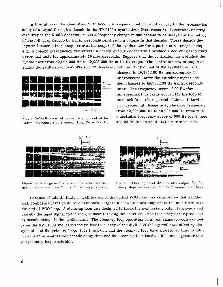
A limitation on the generation of an accurate frequency output is introduced by the propagation delay of a signal through a decade in the HP 5100A synthesizer (Reference 5). Bandwidth-limiting circuitry in the 5100A decades causes a frequency change in one decade to be delayed at the output of the following decade by 4 microseconds relative to a change in that decade. These decade de- lays will cause a frequency e r r o r at the output of the synthesizer for a period of 4 psec/decade; e.g., a change in frequency that effects a change of four decades will produce a declining frequency e r r o r that lasts for approximately 16 microseconds. Suppose that the controller has switched the synthesizer f rom 49,995,000 Hz to 49,995,090 Hz in 10 Hz steps. The controller now attempts to switch the synthesizer to 49,995,100 Hz; however, the frequency output of the synthesizer first
changes to 49,995,190 Hz approximately 2
0.1 SEC f rom 49,995,990 Hz to 49,996,000 Hz resul ts in a declining frequency e r r o r of 990 Hz for 4 psec and 90 HZ fo r an additional 4 microseconds.
Figure 6-Osci I logram of phase detector output for "down" frequency step changes. LOOP BW = 277 Hz.
0.1 SEC
H 0.1 SEC
H
Figure 7-Oscillogrom of discriminator output for fre- Figure 8-Oscillogram of discriminator output for fre- quency steps less than "pullout" frequency of loop. quency steps greater than "pullout" frequency of loop.
Because of this limitation, modification of the digital VCO loop w a s required so that a high- lock confidence level could be established. Figure 9 shows a block diagram of the modification to the digital VCO loop. A clean-up loop was designed to track the synthesizer output frequency and thereby the input signal to the loop, without tracking the short-duration frequency e r r o r produced by decade delays in the synthesizer. The clean-up loop operating on a high signal-to-noise output f rom the HP 5100A increases the pullout frequency of the digital VCO loop while not affecting the dynamics of the primary loop. It is important that the clean-up loop have a response time greater than the total synthesizer decade delay time and the clean-up loop bandwidth be much greater than the primary loop bandwidth.
6
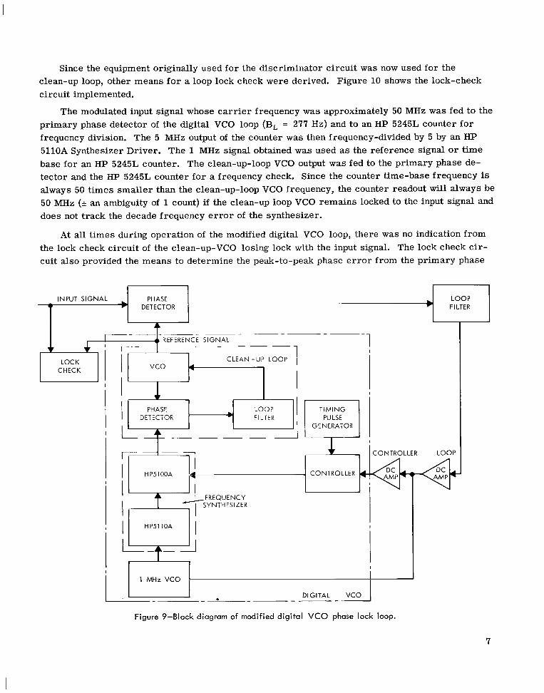
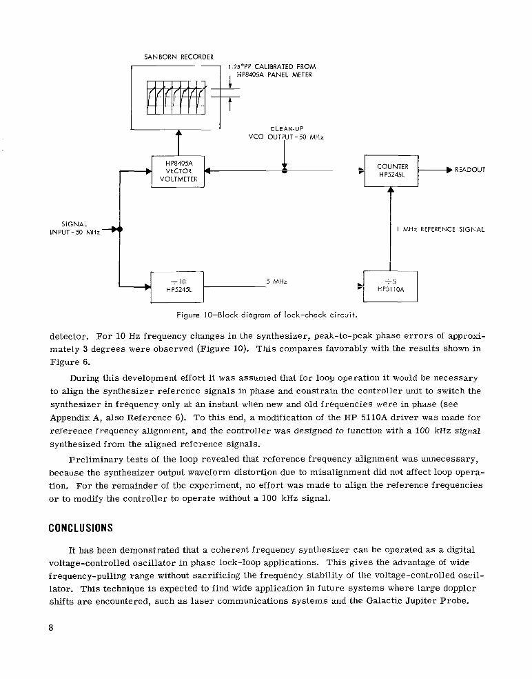
Since the equipment originally used for the discriminator circuit was now used for the clean-up loop, other means fo r a loop lock check were derived. Figure 10 shows the lock-check circuit implemented.
The modulated input signal whose ca r r i e r frequency was approximately 50 MHz was fed to the primary phase detector of the digital VCO loop (BL = 277 Hz) and to an H P 5245L counter for frequency division. The 5 MHz output of the counter was then frequency-divided by 5 by an H P 5110A Synthesizer Driver. The 1 MHz signal obtained was used as the reference signal o r t ime base for an H P 5245L counter. The clean-up-loop VCO output was fed to the primary phase de- tector and the HP 5245L counter fo r a frequency check. Since the counter time-base frequency is always 50 t imes smaller than the clean-up-loop VCO frequency, the counter readout will always be 50 MHz (+ an ambiguity of 1 count) if the clean-up loop VCO remains locked to the input signal and does not track the decade frequency e r r o r of the synthesizer.
At a l l t imes during operation of the modified digital VCO loop, there was no indication from the lock check circuit of the clean-up-VCO losing lock with the input signal. The lock check c i r - cuit also provided the means to determine the peak-to-peak phase e r r o r from the primary phase
INPUT SIGNAL DETECTOR
I
REFERENCE SIGNAL
CLEAN -UP LOOP
I
ZONTROLLER LOOP
I
I I 1 MHz V C O
DIGITAL VCO 1 I- - ---
Figure 9-Block diagram of modified digital VCO phase lock loop.
7
SAN BORN RECORDER
1.25’PP CALIBRATED FROM 7 1 , HP8405A PANEL METER
CLEAN-UP VCO OUTPUT - 50 MHz ‘7’
COUNTER READOUT H P5245L
L
1 MHz REFERENCE SIGNAL
H P8405A VECTOR 4
VOLTMETER
SIGNAL INPUT-50 MHz-’
Figure 10-Block diagram of lock-check circuit.
detector. For 10 Hz frequency changes in the synthesizer, peak-to-peak phase e r r o r s of approxi- mately 3 degrees were observed (Figure 10). This compares favorably with the results shown in Figure 6.
During this development effort i t was assumed that for loop operation i t would be necessary to align the synthesizer reference signals in phase and constrain the controller unit to switch the synthesizer in frequency only at an instant when new and old frequencies were in phase (see Appendix A, also Reference 6). To this end, a modification of the HP 5110A driver was made for reference frequency alignment, and the controller was designed to function with a 100 kHz signal synthesized from the aligned reference signals.
Preliminary tes ts of the loop revealed that reference frequency alignment was unnecessary, because the synthesizer output waveform distortion due to misalignment did not affect loop opera- tion. For the remainder of the experiment, no effort was made to align the reference frequencies or to modify the controller to operate without a 100 kHz signal.
CONCLUSIONS
It has been demonstrated that a coherent frequency synthesizer can be operated as a digital voltage-controlled oscillator in phase lock-loop applications. This gives the advantage of wide f requency-pulling range without sacrificing the frequency stability of the voltage-controlled oscil- lator. This technique is expected to find wide application in future systems where large doppler shifts are encountered, such as laser communications systems and the Galactic Jupiter Probe.
8
ACKNOWLEDGMENTS
The authors would like to acknowledge the valuable comments and suggestions made by Mr. Edward H. Johnson and Mr. Vincent J. DiLosa of the Goddard Space Flight Center during the course of this work. Also, we are indebted to Mr. V. R. Simas for h i s help in organizing and editing this paper.
Goddard Space Flight Center National Aeronautics and Space Administration
Greenbelt, Maryland, October 16, 1967 150-22-14-03-51
REFERENCES
1. Sydnor R., "Frequency Stability Requirements for Space Communications and Tracking Systems," PYOC. IEEE, p. 233, Feb. 1966.
2. Gardner, F. M., "Phaselock Techniques," New York: John Wiley, 1966.
3. Karras , T. J., "Equivalent Noise Bandwidth Analysis from Transfer Functions," NASA TN D-2842, November 1965.
4. Viterbi, A. J., "Acquisition and Tracking Behavior of Phase-Locked Loops,'' J P L External Publication No. 673, July 14, 1959.
5. "Fast Switching with Hewlett-Packard Frequency Synthesizer," Hewlett-Packard Internal Report, Dec. 1965.
6. Barry, G. H., and Fenwick, R. B., "Extraterrestrial and Ionospheric Sounding With Synthesized Frequency Sweeps," Hewlett-Packaycl J. 16(11): July 8, 1965.
7. "HP 5100A/5100A Frequency Synthesizer and Synthesizer Driver," Hewlett-Packard Operating and Service Manual, 1965.
9

. . .

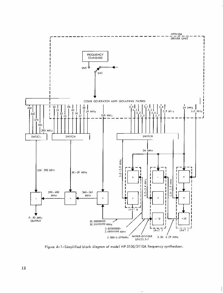
Figure A1 is a simF
Appendix A
Theory o f Operation o f Frequency Synthesizer
ified block diagram of the Hewlett-Packard 5100A/5 10A Frequency Synthesizer (Reference 7). All frequencies shown are generated from an internal 1-MHz standard oscillator in the HP 5110A Driver Unit o r from an external 1 MHz o r 5 MHz standard. The driver unit generates a spectrum of frequencies and then appropriately selects 22 fixed frequencies to drive the HP 5100A synthesizer unit. The HP 5100A synthesizer unit contains harmonic generators, dividers, filters, mixers, and amplifiers that arithmetically manipulate the frequencies generated in the driver unit so as to finally produce the desired synthesizer output frequency.
Figure A1 shows two of seven identical mixer-divider units each of which corresponds to a digit of selected output. The mixer divider-unit at the extreme right of the figure produces the least significant digit of the selected frequency. The 24 MHz signal is mixed with 3 MHz to produce 27 MHz, which is then mixed with a selected frequency between 3.0 and 3.9 MHz, a range divided into 100 kHz increments. The selection of this frequency determines the least significant digit of the synthesizer output frequency. The output of the second mixer is therefore a frequency between 30.0 and 30.9 MHz. This frequency is then divided so as to produce a signal between 3.00 and 3.09 MHz. The synthesis process then repeats itself when this frequency is mixed with 24 MHz in the first mixer of the second mixer-divider unit shown. The mixer output frequency of 27.00 to 27.09 MHz is then mixed with a selected. frequency within the 3.0 to 3.9 MHz range to give a fre- quency within the range of 30.00 to 30.99. The signal is divided to give 3.000 to 3.099 MHz. This process repeats itself five more t imes to obtain a frequency within the range of 3.00000000 to 3.09999999 MHz. Additional mixing produces a signal (0 to 50 MHz) selectable from among 5 billion fixed frequencies all spaced 0.01 Hz apart.
Local selection of the synthesizer output frequency is made at the front panel, by pushbuttons, or remotely, by applying dc voltages to appropriate connector pins at the rear of the HP 5100A synthesizer unit. Either method provides a switching voltage for a diode matrix that selects the appropriate reference frequency (3.0 to 3.9 MHz) to be applied to the mixer-divider unit to produce the digit desired.
The reference signals (3.0 to 3.9 MHz), from which all synthesizer frequencies are derived, a r e produced in the HP 5110A driver by frequency-multiplication of the 1 MHz standard and by filtering and f requency-dividing a selected harmonic. Frequency division produces randomly phased reference signals. In order to produce a continuous variation of the synthesizer output fre- quency without distortion, it is necessary to make a numerically ordered selection of phase- coherent reference signals. To achieve this, it is necessary to align the reference signals so that
11
I I I I I I I I I I I I I I I I I
370
380
390 MHz
INTb i' + COMB GENERATOR AND ISOLATING FILTERS
39 MHz
---
I
I .A0 - 390 MHz 30-39 MHz
1 SWITCH L
N
2 0:
9 r-7 I
0
24
r rl-f -,; I
I1 I + y; I I r
Hz
T I I I I I I I
r - It-
MHz 3.(
--
-1 - 1
I
I I I I I I I I I I I I I I I I I
M H z l , I - - J
I ! I + f I I I I I I I I I I
I I I I I I
? + I
3.09999999 3.00000000- MHz '/ / L7NY7J/ UNIT 1
3.000-3.099MHz 3.00 - 3.09 MHz UNITS 3-7
Figure A-1-Simplified block diagram of model HP 5100/5110A frequency synthesizer.
12

a reference signal is selected at the instant when it and the preceding reference signals are in phase. Since the reference signals a r e 100 kHz apart in frequency, they would be phase-coherent every 10 microseconds.
NASA-I.an$ley. 1968 - 9 13

mIlllI I1 Ill Ill
NATIONAL AERONAUTICS AND SPACE ADMINISTRATION WASHINGTON, D. C. 20546
OFFICIAL BUSINESS
E
FIRST CLASS MAIL
POSTAGE AND FEES PAID NATIONAL AERONAUTICS AND
SPACE ADMINISTRATION
‘ T h e aeronautical and space activities of the United States shall be conducted so as to contribute , . . to the expansion of human knowl- edge of phenonzena in the atmosphere and space. T h e Administration shall provide for the widest prncticable and appropriate dissemination of information concerning its activities and the results thereof.”
-NATIONAL AERONAUTICS AND SPACE ACT OF 1958
NASA SCIENTIFIC AND TECHNICAL PUBLICATIONS
TECHNICAL REPORTS: Scientific and technical information considered important, complete, and a lasting contribution to existing knowledge.
TECHNICAL NOTES: Information less broad in scope but nevertheless of importance as a contribution to existing knowledge.
TECHNICAL MEMORANDUMS : Information receiving limited distribution because of preliminary data, security classifica- tion, or other reasons.
CONTRACTOR REPORTS: Scientific and technical information generated under a NASA contract or grant and considered an important contribution to existing knowledge.
TECHNICAL TRANSLATIONS: Information published in a foreign language considered to merit NASA distribution in English.
SPECIAL PUBLICATIONS: Information derived from or of value to NASA activities. Publications include conference proceedings, monographs, data compilations, handbooks, sourcebooks, and special bibliographies.
TECHNOLOGY UTILIZATION PUBLICATIONS: Information on technology used by NASA that may be of particular interest in commercial and other non-aerospace applications. Publications include Tech Briefs, Technology Utilization Reports and Notes, and Technology Surveys.
Details on the availability of these publications may be obtained from:
SCIENTIFIC AND TECHNICAL INFORMATION DIVISION
NATIONAL AERO N AUT1 C S AND SPACE ADM I N ISTRATI O N Washington, D.C. PO546