9/20/6Lecture 3 - Instruction Set - Al1 Interfacing Devices to the 68000.
18
9/20/6 Lecture 3 - Instruction Set - Al 1 Interfacing Devices to the 68000
-
Upload
alexis-summers -
Category
Documents
-
view
223 -
download
0
Transcript of 9/20/6Lecture 3 - Instruction Set - Al1 Interfacing Devices to the 68000.

9/20/6 Lecture 3 - Instruction Set - Al 1
Interfacing Devices to the 68000
9/20/6 Lecture 3 - Instruction Set - Al 2
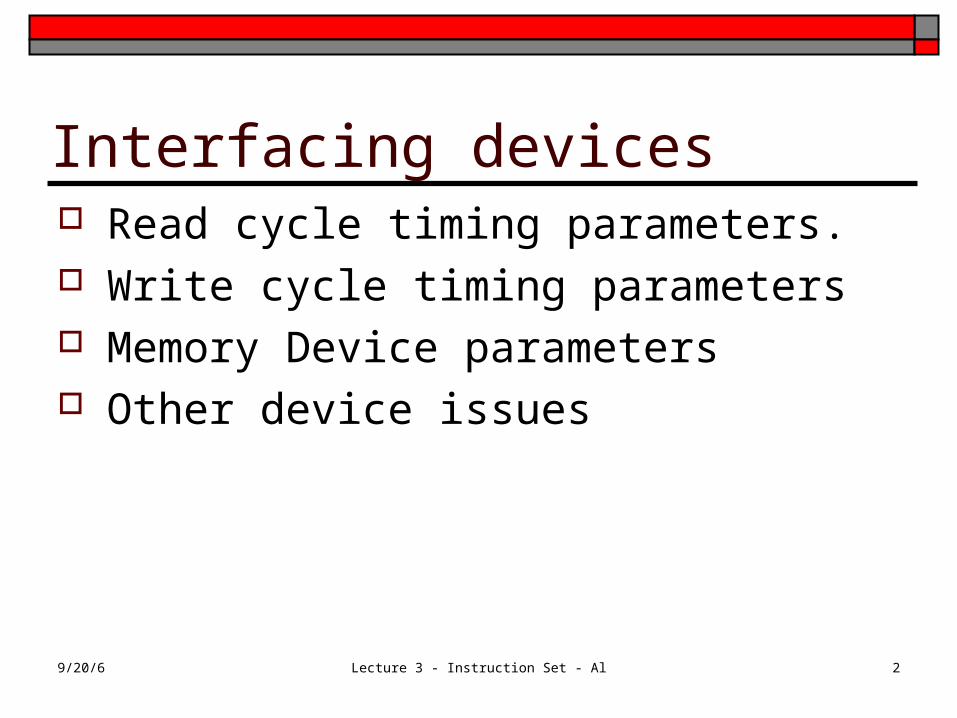
Interfacing devices Read cycle timing parameters. Write cycle timing parameters Memory Device parameters Other device issues

9/20/6 Lecture 3 - Instruction Set - Al 3
Read cycle timing For interfacing the
arrows matter Indicate the
precedence of signals for interfacing

9/20/6 Lecture 3 - Instruction Set - Al 4
Timing continued For a slower
device How fast/slow a
device can be interfaced?
tDALDI is 0 to 90ns But this is FROM
memory

9/20/6 Lecture 3 - Instruction Set - Al 5
Parameters Read cycle parameters

9/20/6 Lecture 3 - Instruction Set - Al 6
Memory timing Must consider timing
of memory device

9/20/6 Lecture 3 - Instruction Set - Al 7
Memory Pinout of the 6116 static RAM

9/20/6 Lecture 3 - Instruction Set - Al 8
Items of note Chip is 2K x 8-bit Data word is a byte Must use LDS* and UDS* when configuring
memory with the device In general memory chips are 1-bit, 1-byte, or
1-word in width of the data interface.

9/20/6 Lecture 3 - Instruction Set - Al 9
Connecting up the 6116
9/20/6 Lecture 3 - Instruction Set - Al 10
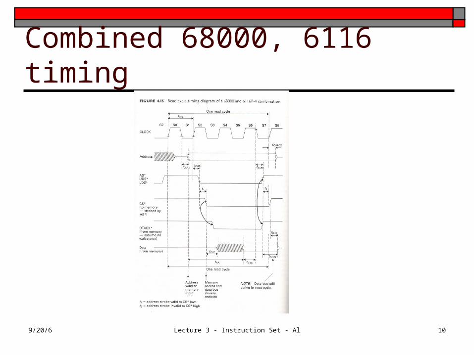
Combined 68000, 6116 timing
Stop here on Mon
9/20/6 Lecture 3 - Instruction Set - Al 11

9/20/6 Lecture 3 - Instruction Set - Al 12
The write cycle Timing of processor and memory device must
work for both reading device and writing device It is possible that timing will work for read but
not for write for a given device I/O devices may be such that they are only
written to or read from Example: On modern motherboards you may
need matched DIMMs in pairs for the faster memory access speeds. (4GB Dual Channel DDR3 RAM – PC12800, 1600MHz (2x2048MB)
9/20/6 Lecture 3 - Instruction Set - Al 13
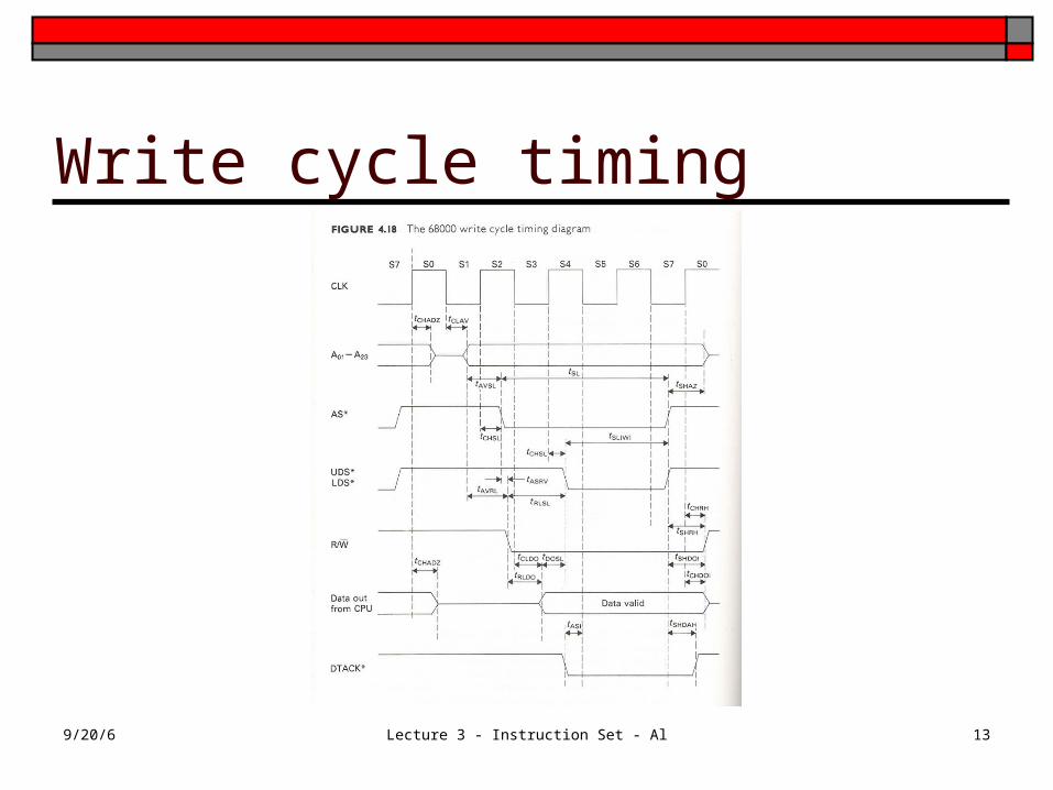
Write cycle timing

9/20/6 Lecture 3 - Instruction Set - Al 14
Write cycle parameters
9/20/6 Lecture 3 - Instruction Set - Al 15
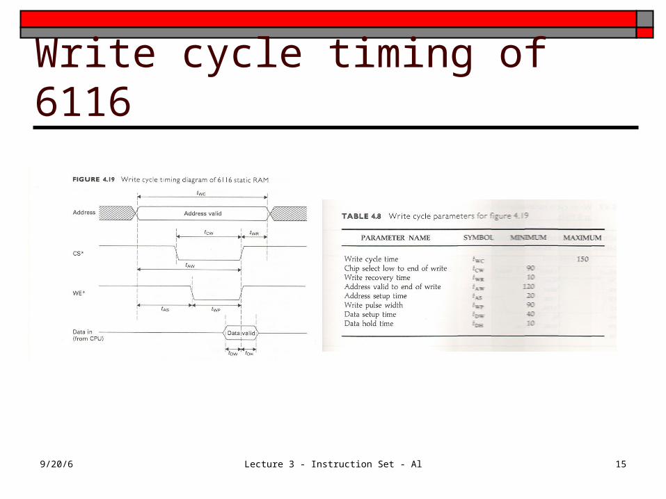
Write cycle timing of 6116

9/20/6 Lecture 3 - Instruction Set - Al 16
68000-6116 combination for write
9/20/6 Lecture 3 - Instruction Set - Al 17
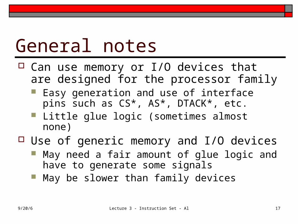
General notes Can use memory or I/O devices that are
designed for the processor family Easy generation and use of interface pins such as
CS*, AS*, DTACK*, etc. Little glue logic (sometimes almost none)
Use of generic memory and I/O devices May need a fair amount of glue logic and have to
generate some signals May be slower than family devices

9/20/6 Lecture 3 - Instruction Set - Al 18
General methodology Read cycle timing parameters and specifically
those that matter in device interfacing Then the same for write Memory chip timing parameters and how they
matches (or don’t) with what we havd