9/20/6Lecture 12 - Interfacing Devices1 Interfacing Devices to the 68000.
Upload
micah-fullenCategory
view
221download
1
9/20/6 Lecture 3 - Instruction Set - Al 1
The Hardware Interface

9/20/6 Lecture 3 - Instruction Set - Al 2
The Hardware Interface The 68000 Hardware Interface
Chip Pins – group pins into classes Specifics of the classes – look at each class of
pins in turn Some basic interfacing to those pins

9/20/6 Lecture 3 - Instruction Set - Al 3
Chip Interfaces Chip interface for a microprocessor
Microprocessor chip is not stand alone To make it work must add
Memory I/O interfaces Timing Other support pin connections that are processor
specific Support pins like RESET

9/20/6 Lecture 3 - Instruction Set - Al 4
Microprocessors and microcontrollers What is the difference in a microprocessor and a
microcontroller? Microprocessor – needs memory, I/O, and other
support to operate. Microcontroller – almost stand alone
Many have internal clock – can add an external crystal if desired but usually not required
RAM and ROM on the chip (although limited in size) I/O on chip – often dual use for I/O and address/data
to/from memory Minimal external support needed

9/20/6 Lecture 3 - Instruction Set - Al 5
The 68000 pinout 64 pin chip Pins can be placed
into 3 categories System support Special purpose
Usually device specific
Memory and peripheral interface
9/20/6 Lecture 3 - Instruction Set - Al 6
System support pins Most are common to all microprocessor and
microcontroller chips Power Supply
68000 has 2 each Vcc and GND pins (4 total) Why?
Better on chip power distribution and thus, a more reliable chip.
Less voltage drop to many points on the chip

9/20/6 Lecture 3 - Instruction Set - Al 7
System support pins - 2 Clock
Single phase TTL-compatible signal All internal timing derived for this signal 68000 uses dynamic storage technique internally
What is dynamic storage technique? VLSI technique that reduces the logic required and
thus results in power savings Relies on the capacitive nature of CMOS VLSI

9/20/6 Lecture 3 - Instruction Set - Al 8
System support pins - 3 2 Phase Clock
operation Non overlapping
Only 1 high at any time When asserted
Input value applied Value is then held by
the capacitive charge on the output, signal line, and gate input
1 2
1
2
ENB ENB
9/20/6 Lecture 3 - Instruction Set - Al 9
System support pins - 4 RESET* (* means active low)
Common to all microprocessors and microcontrollers
Forces processor into a known state Reset action on the 68000
Load the supervisor stack pointer from memory location $00 0000 and loads the PC from address $00 0004
RESET* and HALT* asserted for at least 100ms for correct reset action to be initiated when they are no longer asserted.
9/20/6 Lecture 3 - Instruction Set - Al 10
System support pins - 5 RESET* also acts as an output to allow reset of
other system devices
HALT* (also a bidirectional pin) Active low When asserted by external device, causes 68000
to stop processing at end of current bus cycle and tristate data and address busses

9/20/6 Lecture 3 - Instruction Set - Al 11
System support pins - 6 HALT*
Enables the 68000 to execute a single bus cycle each time asserted
Thus allows the processor to be stepped through the program cycle by cycle.
USEFUL FOR DEBUGGING Cycle by cycle is not common but instruction by
instruction is present in most microprocessors and microcontrollers
Halt can also be an output to indicate error conditions

9/20/6 Lecture 3 - Instruction Set - Al 12
Special Function Pins BERR*
Bus error input (active low) Informs the processor that something has gone
wrong with the current bus cycle Allows for “graceful” recovery if possible
Action taken is complex and also dependent on HALT*
9/20/6 Lecture 3 - Instruction Set - Al 13
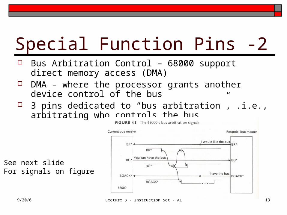
Special Function Pins -2 Bus Arbitration Control – 68000 support direct memory
access (DMA) DMA – where the processor grants another device control of
the bus 3 pins dedicated to “bus arbitration”, .i.e., arbitrating who
controls the bus
See next slideFor signals on figure

9/20/6 Lecture 3 - Instruction Set - Al 14
Special Function Pins - 3 Bus arbitration pins
BR* - Bus Request – when asserted informs the CPU that another device wishes to take control of the system bus.
BG* - Bus Grant – an output from the 68000. When asserted tell the device that asserted BR* that it is being granted control of the bus. When this device is done with the bus it must deassert its BR signal
BGACK* - Bus Grant Acknowledge – and input that tells the 68000 that the device wishing control and granted control, acknowledges that it now the bus master.
9/20/6 Lecture 3 - Instruction Set - Al 15
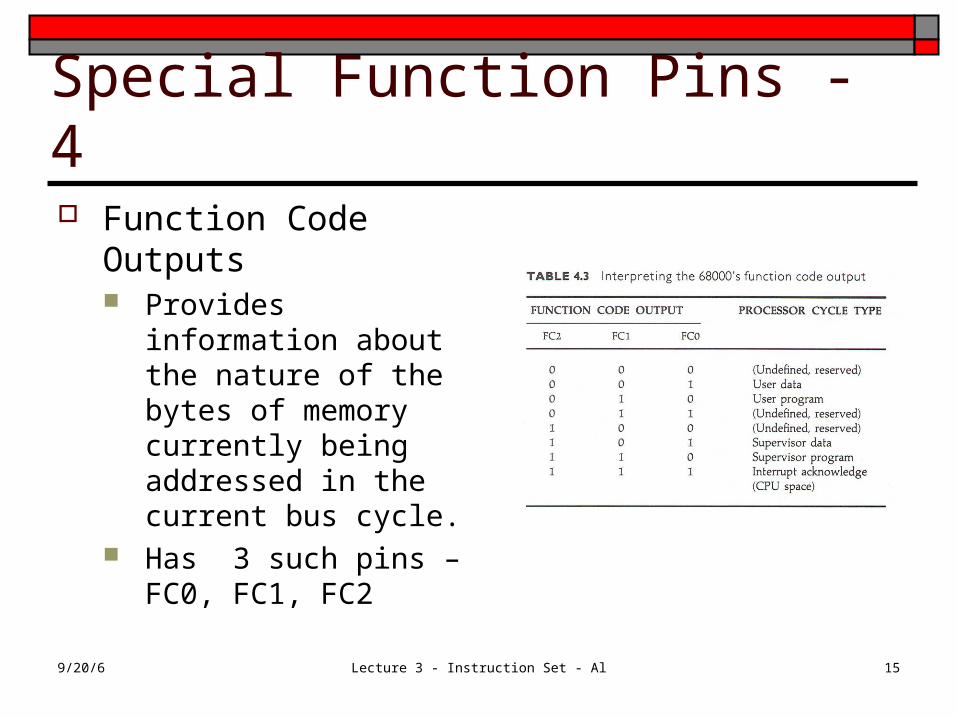
Special Function Pins - 4 Function Code Outputs
Provides information about the nature of the bytes of memory currently being addressed in the current bus cycle.
Has 3 such pins – FC0, FC1, FC2
9/20/6 Lecture 3 - Instruction Set - Al 16
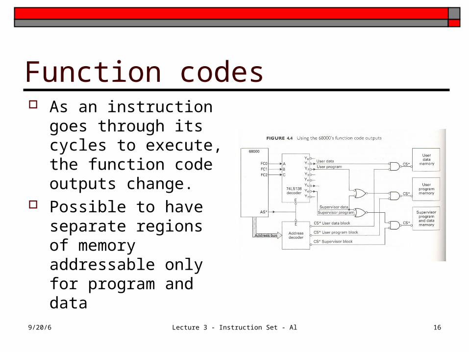
Function codes As an instruction goes
through its cycles to execute, the function code outputs change.
Possible to have separate regions of memory addressable only for program and data

9/20/6 Lecture 3 - Instruction Set - Al 17
Special Function Pins - 5 Interrupt control Interfaces 3 interrupt control inputs
IPL0*, IPL1*, IPL2* 3 input pins allow 8 level for setting priority on
devices requesting interrupt in hardware. Allows servicing the more important request
when multiple requests arrive during the same cycle.
Level 7 – all pins asserted – always serviced

9/20/6 Lecture 3 - Instruction Set - Al 18
Special Function Pins - 6 Interrupts can be masked off Bits 8,9, & 10 of the status word indicate the
level of interrupt that will be serviced Priority of interrupt must be equal to or
greater than this level to be serviced So level 7 is highest (IPL0*, IPL1*, IPL2* all
asserted). Level 6 next where (IPL0*, IPL1*, IPL2).