90 Degree Hybrid Coupler - Worcester Polytechnic Institute · PDF fileAdditionally...
127
90 Degree Hybrid Coupler By __________________________________ James Corsini __________________________________ Josué Malaver ___________________________________ Sokol Lushllari Date: April 25, 2013 Major Qualifying Project submitted to the Faculty of WORCESTER POLYTECHNIC INSTITUTE In partial fulfillment of the requirements for the degree of Bachelor of Science Approved: ______________________________ Professor Reinhold Ludwig ______________________________ Professor John McNeill ______________________________ David Whitefield
Transcript of 90 Degree Hybrid Coupler - Worcester Polytechnic Institute · PDF fileAdditionally...

90 Degree Hybrid Coupler
By
__________________________________
James Corsini
__________________________________
Josué Malaver
___________________________________
Sokol Lushllari
Date: April 25, 2013
Major Qualifying Project submitted to the Faculty of
WORCESTER POLYTECHNIC INSTITUTE
In partial fulfillment of the requirements for the degree of
Bachelor of Science
Approved:
______________________________
Professor Reinhold Ludwig
______________________________
Professor John McNeill
______________________________
David Whitefield

Worcester Polytechnic Institute
Page | ii
Abstract
In this Major Qualifying Project we were tasked by our project sponsor, Skyworks
Solutions Inc., to redesign a 90-hybrid coupler with the center frequency of 1.9GHz. The
sponsor’s requirements for the new design were to increase the bandwidth and decrease the
device area. Both of these requirements were met by developing a theoretical model and were
then validated by simulations in Agilent’s ADS. Additionally Ansys’ HFSS was used to model
the new design in a 3-D environment where the electric and magnetic radiation fields can be
studied. This was a necessary step in order to develop a model accounting for interference
originating from the device. Step by step tutorials were created so that the reader can better
understand how to implement the developed models in these simulators. The final design yielded
a bandwidth increase of 150% with an area reduction of 63%.

Worcester Polytechnic Institute
Page | iii
Acknowledgements
We would like to thank Dr. Whitefield and the Skyworks Inc. team, without whom this
project would not exist. Specifically, we would like to thank Eric Austin for his knowledge and
guidance with the measurements taken at the Skyworks laboratory. Special thanks to our advisor
Professor Reinhold Ludwig and our co-advisor Professor John McNeill for their constant
guidance and motivation. Also, thanks to Jeffery Elloian who was extremely helpful with the
HFSS simulations.

Worcester Polytechnic Institute
Page | iv
Table of Contents
Abstract ........................................................................................................................................... ii
Acknowledgements ........................................................................................................................ iii
Table of Figures ............................................................................................................................. vi
Table of Tables .............................................................................................................................. ix
Acronym List .................................................................................................................................. x
1 Introduction ........................................................................................................................... 11
2 Background ............................................................................................................................ 12
2.1 Organization of MQP report .......................................................................................... 12
2.2 What are 90 degree hybrid couplers? ............................................................................. 12
2.3 Design topologies ........................................................................................................... 14
2.3.1 Distributed elements ............................................................................................... 15
2.3.2 Lumped elements .................................................................................................... 16
2.4 Current problems of 90 degree hybrid couplers in microelectronic circuits .................. 18
2.5 S-Parameters, ABCD-Matrix Description...................................................................... 18
2.5.1 Scattering parameters .............................................................................................. 19
2.5.2 ABCD Parameters ................................................................................................... 21
2.6 Even and Odd Mode Analysis ........................................................................................ 23
2.7 Network Analyzer Measurements .................................................................................. 25
3 Goal of Project ....................................................................................................................... 27
4 Theoretical Analysis .............................................................................................................. 28
5 New design approach ............................................................................................................. 34
6 Simulations ............................................................................................................................ 42
6.1 Simulation and data analysis tools ................................................................................. 42
6.1.1 High Frequency Structural Simulator (HFSS) ........................................................ 42
6.1.2 Advanced Design Systems (ADS) .......................................................................... 42
6.1.3 Matlab ..................................................................................................................... 43
7 Computational Analysis ........................................................................................................ 44
7.1 ADS Simulations ............................................................................................................ 44
7.2 Capacitor and spiral inductor calculations ..................................................................... 46

Worcester Polytechnic Institute
Page | v
7.3 Step By Step ADS Layout .............................................................................................. 48
7.3.1 Momentum Results ................................................................................................. 76
7.4 Step by step layout instructions for HFSS ..................................................................... 78
7.4.1 HFSS Results ........................................................................................................ 105
8 Results ................................................................................................................................. 109
9 Conclusion ........................................................................................................................... 110
10 Future Improvements ....................................................................................................... 111
Appendix A ................................................................................................................................. 112
Appendix B ................................................................................................................................. 120
Appendix C ................................................................................................................................. 122
Appendix D ................................................................................................................................. 124
Bibliography ............................................................................................................................... 126

Worcester Polytechnic Institute
Page | vi
Table of Figures
Figure 1: Block diagram of 90 Degree hybrid coupler feeding into LNAs .................................. 13
Figure 2: Branch line hybrid coupler ............................................................................................ 15
Figure 3: Coupled transmission tine hybrid coupler ..................................................................... 16
Figure 4: Pi and T network configurations ................................................................................... 17
Figure 5: Current design at Skyworks for 90 degree hybrid coupler ............................................ 17
Figure 6: Two port S-parameter network...................................................................................... 19
Figure 7: 4x4 S-parameter matrix ................................................................................................. 21
Figure 8: Two-Port network, analyzed with ABCD parameters................................................... 22
Figure 9: Cascading two networks ................................................................................................ 22
Figure 10: Quad Hybrid connected with a supply voltage ........................................................... 23
Figure 11: Quad-Hybrid symmetrically split ................................................................................ 23
Figure 12: EVEN mode configuration, open TL .......................................................................... 24
Figure 13: ODD mode, grounded TL ........................................................................................... 24
Figure 14: Thru TL using electronic calibration ........................................................................... 25
Figure 15: S21 and S31 magnitude using electronic calibration .................................................. 26
Figure 16: Phase difference using electronic calibration ............................................................. 26
Figure 17: Amplitude difference using electronic calibration ...................................................... 26
Figure 18: TL stubs ....................................................................................................................... 28
Figure 19: The new design quad hybrid ....................................................................................... 34
Figure 20: Microstrip Z0 as function of w/h (Z02)......................................................................... 35
Figure 21: Microstrip Z0 as function of w/h (Z01)......................................................................... 37
Figure 22: The quad hybrid implemented in ADS........................................................................ 38
Figure 23: TL to Lumped component conversion ........................................................................ 38
Figure 24: TL representation for T1A & T1B .............................................................................. 39
Figure 25: Lumped equivalent for TL T1A & T1B ...................................................................... 39
Figure 26: TL representation for T2A & T2B .............................................................................. 39
Figure 27: Lumped equivalent for TL T2A & T2B ...................................................................... 40
Figure 28: The lumped equivalent circuit of the quad hybrid ...................................................... 40
Figure 29: Final Lumped equivalent circuit.................................................................................. 41
Figure 30: Lumped equivalent circuit ........................................................................................... 44
Figure 31: The phase difference of two output ports .................................................................... 45
Figure 32: The 3dB attenuation of the two output ports ............................................................... 46
Figure 33: Start Agilent's Advanced Design System .................................................................... 48
Figure 34: Create a new workspace .............................................................................................. 49
Figure 35: Chose appropriate location to store all files ................................................................ 50
Figure 36: Select the desired libraries ........................................................................................... 51
Figure 37: Create your own library ............................................................................................... 51
Figure 38: Select default units ...................................................................................................... 52

Worcester Polytechnic Institute
Page | vii
Figure 39: Starting new layout ...................................................................................................... 53
Figure 40: Creating layers ............................................................................................................. 53
Figure 41: Layer properties ........................................................................................................... 54
Figure 42: Layer preferences window .......................................................................................... 55
Figure 43: Insert path .................................................................................................................... 56
Figure 44: Creating an inductor .................................................................................................... 58
Figure 45: Creating the top plate of the capacitor ......................................................................... 59
Figure 46: Top plates for capacitors ............................................................................................. 60
Figure 47: Input pads .................................................................................................................... 61
Figure 48: Bottom capacitors ........................................................................................................ 62
Figure 49: Changing the transparency .......................................................................................... 63
Figure 50: Bottom inductor ........................................................................................................... 64
Figure 51: Bottom of the port connectors ..................................................................................... 65
Figure 52: Making connections .................................................................................................... 66
Figure 53: Schematic reference .................................................................................................... 67
Figure 54: Finalized design ........................................................................................................... 68
Figure 55: Substrate setup ............................................................................................................. 69
Figure 56: Inserting a conducting layer ........................................................................................ 70
Figure 57: Inserting layers above/below ....................................................................................... 71
Figure 58: Inserting conductor VIA .............................................................................................. 72
Figure 59: Completed substrate .................................................................................................... 73
Figure 60: 3-D Model ................................................................................................................... 74
Figure 61: Frequency plan ............................................................................................................ 75
Figure 62: New ADS design results.............................................................................................. 76
Figure 63: Phase plot for new design ............................................................................................ 77
Figure 64: Drawing the spiral inductor ......................................................................................... 79
Figure 65: Setting variables to spiral ............................................................................................ 80
Figure 66: Spiral inductor ............................................................................................................. 81
Figure 67: Double spirals .............................................................................................................. 82
Figure 68: Capacitor and bondpad after correction ...................................................................... 83
Figure 69: Creating capacitors and bondpads ............................................................................... 84
Figure 70: Connector 1 box 1 ....................................................................................................... 85
Figure 71: Connector 1 box 2 ....................................................................................................... 86
Figure 72: Connector 1 complete .................................................................................................. 87
Figure 73: All of the connectors ................................................................................................... 91
Figure 74: United circuit ............................................................................................................... 92
Figure 75: Creating ground plane ................................................................................................. 93
Figure 76: Making ground stubs ................................................................................................... 94
Figure 77: Creating and assigning lumped ports .......................................................................... 95
Figure 78: Assigning the integral line for a lumped port .............................................................. 96

Worcester Polytechnic Institute
Page | viii
Figure 79: Creating oxide layer .................................................................................................... 97
Figure 80: Creating a passivation layer ........................................................................................ 98
Figure 81: Creating a substrate layer ............................................................................................ 99
Figure 82: Box of air around everything..................................................................................... 100
Figure 83: Selecting all face of the box of air ............................................................................. 101
Figure 84: Using PML wizard .................................................................................................... 102
Figure 85: 3D HFSS model......................................................................................................... 105
Figure 86: HFSS electric field plot ............................................................................................. 106
Figure 87: HFSS electric field plot (cross-sectional) .................................................................. 106
Figure 88: HFSS s-parameter magnitude .................................................................................... 107
Figure 89: HFSS s-parameter phase difference .......................................................................... 108
Figure A.1: Hybrid Coupler 2 S21 and S31 Magnitude (dB) ........................................................ 115
Figure A.2: Hybrid Coupler 2 S21 and S31 Amplitude Difference .............................................. 115
Figure A.3: Hybrid Coupler 2 S21 and S31 Phase Difference (degrees) ...................................... 115
Figure A.4: Hybrid Coupler 3 S21 and S31 Magnitude (dB) ........................................................ 115
Figure A.5: Hybrid Coupler 3 S21 and S31 Amplitude Difference .............................................. 116
Figure A.6: Hybrid Coupler 3 S21 and S31 Phase Difference (degrees) ...................................... 116
Figure A.7: Hybrid Coupler 3 S21 and S31 Magnitude (dB) ........................................................ 116
Figure A.8: Hybrid Coupler 4 S21 and S31 Amplitude Difference .............................................. 116
Figure A.9: Hybrid Coupler 4 S21 and S31 Phase Difference (degrees) ...................................... 116
Figure A.10: Hybrid Coupler 1 S21 and S31 Magnitude (dB) ...................................................... 118
Figure A.11: Hybrid Coupler 1 S21 and S31 Amplitude Difference ............................................ 118
Figure A.12: Hybrid Coupler 1 S21 and S31 Phase Difference (degrees) .................................... 118
Figure A.13: Hybrid Coupler 2 S21 and S31 Magnitude (dB) ...................................................... 118
Figure A.14: Hybrid Coupler 2 S21 and S31 Amplitude Difference ............................................ 118
Figure A.15: Hybrid Coupler 2 S21 and S31 Phase Difference (degrees) .................................... 118
Figure A.16: Hybrid Coupler 3 S21 and S31 Magnitude (dB) ...................................................... 119
Figure A. 17: Hybrid Coupler 3 S21 and S31 Amplitude Difference ........................................... 119
Figure A. 18: Hybrid Coupler 3 S21 and S31 Phase Difference (degrees) ................................... 119
Figure A. 19: Hybrid Coupler 4 S21 and S31 Magnitude (dB) ..................................................... 119
Figure A. 20: Hybrid Coupler 4 S21 and S31 Amplitude Difference ........................................... 119
Figure A. 21: Hybrid Coupler 4 S21 and S31 Phase Difference (degrees) ................................... 119
Figure C.1: Appendix: 3D polar plot .......................................................................................... 122
Figure C.2: Appendix: Directivity .............................................................................................. 122
Figure C.3: Appendix: XY gain plot........................................................................................... 123
Figure D.4: Conversion between different network representations [7] ..................................... 124
Figure D.5: ABCD-parameters of several two-port circuits [7] ................................................. 125

Worcester Polytechnic Institute
Page | ix
Table of Tables
Table 1: List of connection coordinates and sizes ........................................................................ 88
Table 2: Comparison of Skyworks model to WPI design........................................................... 109

Worcester Polytechnic Institute
Page | x
Acronym List
MQP Major Qualifying Project
IEEE Institute of Electrical and Electronics Engineers
RF Radio Frequency
MW Microwaves
LNA Low noise amplifier
MMIC Monolithic microwave integrated circuit
ADS Advanced Design System
HFSS High Frequency Structural Simulator
S-parameter Scattering Parameters
FEM Finite Element Method
TL Transmission Lines

Worcester Polytechnic Institute
Page | 11
1 Introduction
Skyworks Inc. has sponsored a Major Qualifying Project (MQP) to investigate and
redesign its current 90-degree hybrid coupler. It is one of the world’s leading innovators in high
performance analog and mixed signal semiconductors and offers a wide variety of products.
These products are used in military, medical, automotive, and handset applications around the
world [1]. Specifically, the 90 degree hybrid coupler is utilized in the handset infrastructure
because it offers low-loss, high isolation, and exceptional phase and amplitude balance.
The demand for a smaller 90-degree hybrid coupler with a broader bandwidth is
proliferating at a quick pace in order to keep up with a rapidly advancing communication
industry. Skyworks has deemed the 90-degree hybrid coupler as a product of extreme interest
for further development, and its microelectronic implementation has become the focus of this
MQP. The goal of this project is to create a new design that will improve upon the existing
model in terms of frequency capability while maintaining or decreasing the device size.

Worcester Polytechnic Institute
Page | 12
2 Background
2.1 Organization of MQP report
The first step taken in this project was to understand the physical performance of the 90-
degree hybrid coupler. Throughout this process IEEE journals and several other reputable
articles have been studied to gain a better understanding of this device. Additionally, different
topologies and currently implemented solutions have been investigated to understand what is
state-of-the-art in industry. The current design implemented by the project sponsor Skyworks
was thoroughly analyzed through mathematical analysis, software simulations, and on-site
measurements. Fully understanding different topologies and the current problems of the existing
coupler have provided direction towards the new design approach.
2.2 What are 90 degree hybrid couplers?
Hybrid couplers are four-port devices that split the incident power signal into two output
ports. The signals at the outputs are attenuated by three decibels (3dB) and have a 90 degree
phase difference with respect to each other. Three decibel attenuation means that 50% of the
input power is lost [2]. In addition, reflections due to mismatches are sent to the isolation port
preventing any power from reflecting back to the input port. In addition to splitting a signal they
can also be used to combine power signals with a high degree of isolation between the ports. A
block diagram of this functionality is illustrated in Figure 1.

Worcester Polytechnic Institute
Page | 13
LNA
1LN
A 2
90 DegreeHybrid
Coupler I
90 DegreeHybrid
CouplerII
PORT_1
PORT_4
PORT_2
PORT_3
INPUT
OUTPUT
Г1
Г2
0°
90°
Isolation Port
Isolation Port
Figure 1: Block diagram of 90 Degree hybrid coupler feeding into LNAs
As seen in Figure 1 we have two hybrid couplers attached to two different low noise
amplifiers (LNAs). This is an example of a coupler performing both of its main functions: signal
splitting and combining, while the LNAs do their main job of amplifying the signal. Starting at
port one a power wave is sent and split at the output ports. From there the divided power is fed
to the two LNAs and the amplified outputs are combined together with the second coupler. By
placing a hybrid coupler in front of the LNAs, electrical protection for the components located
before port one is guaranteed because of the hybrid coupler's ability to significantly reduce the
amount of reflected power at the input port. Since there is no reflected power at the input, the
hybrid coupler can also be called a balanced structure circuit. In addition to the aforementioned
functions these devices are vital in communication systems as circuit protectors, perhaps one of
the largest global markets. They can also be used in microwave (MW) phase shifters, antenna
feed systems, driver circuit protection, and in-phase/quadrature (I-Q) modulation / demodulation.
90-degree hybrid couplers are often called branch-line couplers. As the name implies
power is equally divided between the output ports and are therefore electrically and mechanically

Worcester Polytechnic Institute
Page | 14
symmetrical. These branch-line couplers are built using transmission lines and their size is
proportional to the wavelength of the designated center frequency, which can be meters long.
This becomes a significant drawback in applications where a small footprint is required.
Hybrid couplers can also be built by using lumped components, which are resistors,
inductors, and capacitors with an ideal (lossless) connection. The lumped component design is
promising because it provides low insertion loss, wider bandwidth, and a smaller size circuit,
making it a good fit for a monolithic microwave integrated circuit (MMIC) [3].
The best way to describe hybrid couplers is through the use of scattering parameters,
better known as S-parameters. Specifically, these S-parameters describe the signal in terms of
incident and reflected power at the ports of the network. Using the graphs and matrices of the S-
parameters (as seen in section 2.7), it is easy to show the 3dB attenuation of the input signal at
the operating frequency as well as the bandwidth of the hybrid coupler. Agilent’s Advanced
Design Simulator (ADS) provides a method to extract the S-parameters of a device under test.
ADS has been adopted by a vast majority of companies including the project sponsor Skyworks;
it is considered to be an industry standard. For mathematical analysis of the 90-degree hybrid
coupler, a combination of even-odd mode decomposition, S-parameters, and ABCD parameters
is used, which will be discussed in further detail later on.
2.3 Design topologies
There are many design topologies for hybrid couplers [4]. The most common designs are
implemented using transmission lines and lumped elements. In this section, a few topologies are
examined to provide a thorough understanding of the limitations and abilities of each.

Worcester Polytechnic Institute
Page | 15
2.3.1 Distributed elements
A distributed element system is one where the electrical characteristics (resistance,
inductance, capacitance, conductance) of each element in the circuit produce unwanted effects.
To account for these unwanted effects, also known as parasitics, it is required to describe each
element in terms of unit-length. An example of a distributed system is the four port branch line
hybrid coupler with transmission line elements shown in Figure 2.
PORT_1
PORT_3PORT_4
PORT_2
T2A
T1A
T1B
T2B
Figure 2: Branch line hybrid coupler
Each transmission line is designed based on the principle of the lambda quarter transformer,
which yields perfect matching between ports (refer to Appendix for complete
derivation/explanation of the lambda quarter transformer). The length of each transmission line
is dependent upon the center frequency, which is determined by the application. The
characteristic impedance of the parallel transmission lines in the circuit is the same.
Characteristic impedance “is the ratio of the amplitudes of voltage and current of a single wave
propagating along the line” [5] (see section 5). In this scenario, there are two characteristic
impedances, 50Ω and 35.35Ω. Transmission lines T1A and T1B have the same characteristic
impedance, 35.35Ω. Similarly, transmission lines T2A and T2B have the same characteristic
Worcester Polytechnic Institute
Page | 16
impedance of 50Ω. As previously mentioned, all of the transmission lines have approximately
the same length because of the lambda quarter transformation behavior.
A second topology using transmission lines is frequently implemented. In this design two
transmission lines, again using the lambda-quarter transformer, are placed in parallel at very
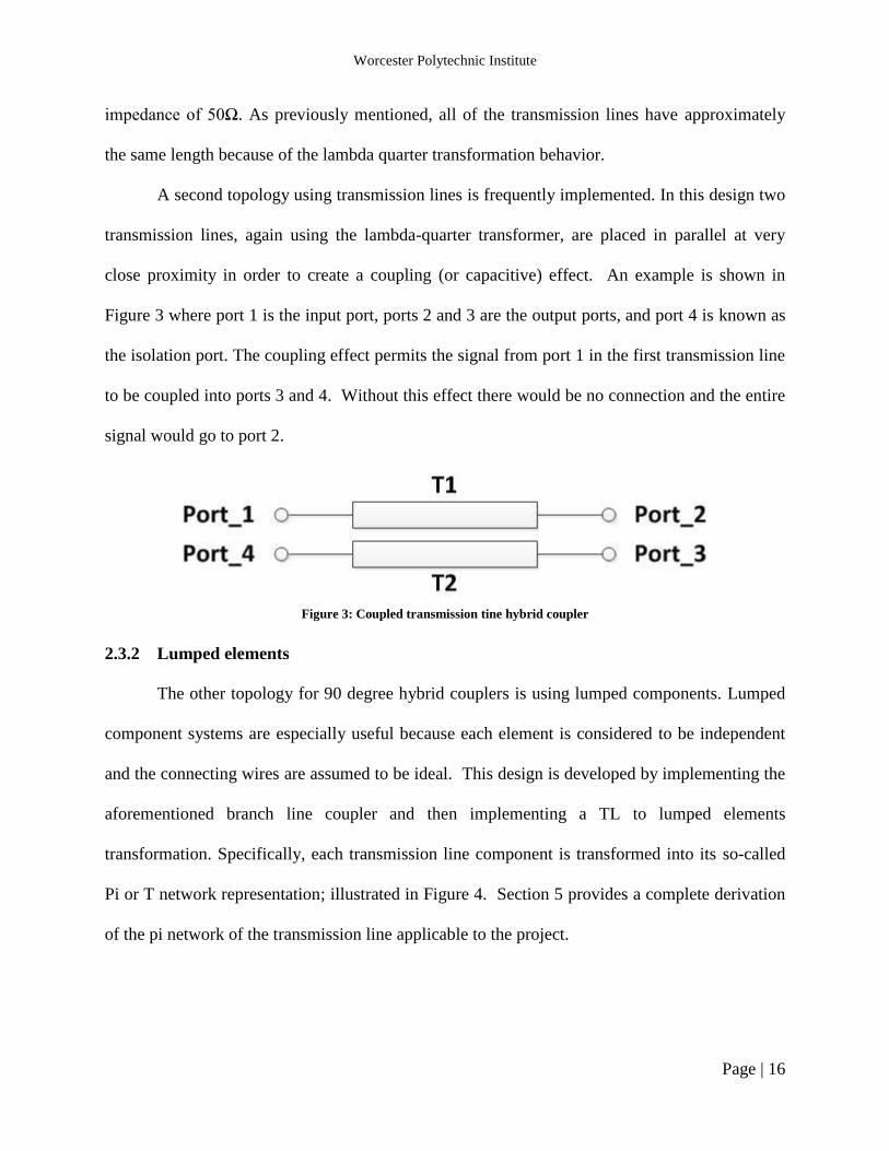
close proximity in order to create a coupling (or capacitive) effect. An example is shown in
Figure 3 where port 1 is the input port, ports 2 and 3 are the output ports, and port 4 is known as
the isolation port. The coupling effect permits the signal from port 1 in the first transmission line
to be coupled into ports 3 and 4. Without this effect there would be no connection and the entire
signal would go to port 2.
Figure 3: Coupled transmission tine hybrid coupler
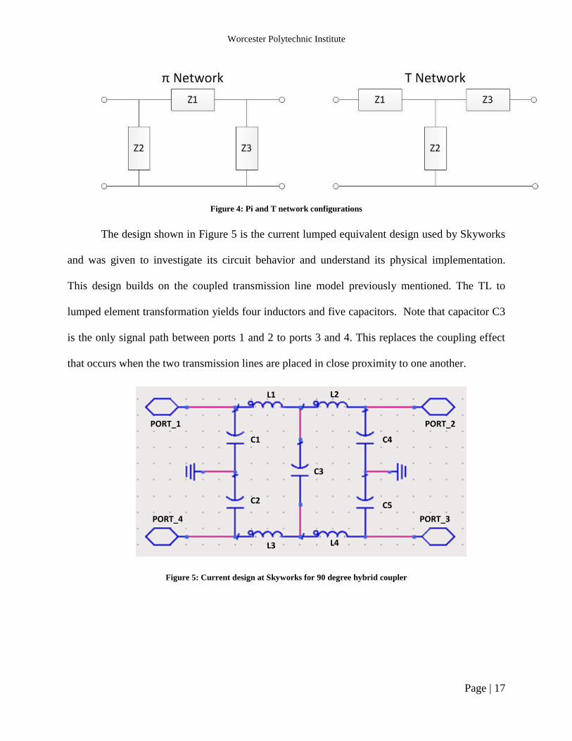
2.3.2 Lumped elements
The other topology for 90 degree hybrid couplers is using lumped components. Lumped
component systems are especially useful because each element is considered to be independent
and the connecting wires are assumed to be ideal. This design is developed by implementing the
aforementioned branch line coupler and then implementing a TL to lumped elements
transformation. Specifically, each transmission line component is transformed into its so-called
Pi or T network representation; illustrated in Figure 4. Section 5 provides a complete derivation
of the pi network of the transmission line applicable to the project.
Worcester Polytechnic Institute
Page | 17
Figure 4: Pi and T network configurations
The design shown in Figure 5 is the current lumped equivalent design used by Skyworks
and was given to investigate its circuit behavior and understand its physical implementation.
This design builds on the coupled transmission line model previously mentioned. The TL to
lumped element transformation yields four inductors and five capacitors. Note that capacitor C3
is the only signal path between ports 1 and 2 to ports 3 and 4. This replaces the coupling effect
that occurs when the two transmission lines are placed in close proximity to one another.
C2
L1
L3
L2
C1
L4
C3
C5
C4
PORT_1 PORT_2
PORT_4 PORT_3
Figure 5: Current design at Skyworks for 90 degree hybrid coupler

Worcester Polytechnic Institute
Page | 18
2.4 Current problems of 90 degree hybrid couplers in microelectronic circuits
A hybrid coupler’s size, cost, interference and bandwidth are often the biggest limitations
in its implementation. Keeping these limitations in mind, manufacturers must provide a diverse
set of designs to satisfy different frequency bands. Noting the overwhelmingly large spectrum of
communication systems, it would be ideal for manufacturers to provide a solution which satisfies
needs over a significant range of these frequencies. A case in which this issue is clearly seen is in
cell phone applications.
Solutions from manufacturers for cell phone applications currently provide bandwidths
between 7% to an ideal of 20% [6]. These bandwidths are quite small, and trying to implement
the same device in other applications with different center frequencies would prove to be non-
functional. It is important to note that 90 degree hybrid couplers are tuned to a specific
frequency, as will be the case even with any improved design. However, if there is a significant
improvement of the bandwidth that can be achieved by these devices, it would prove to be quite
advantageous for both manufacturers and consumers, reducing the cost while increasing
manufacturing efficiency. The main goal is to have one device broad enough to satisfy a wide
range of frequency applications.
2.5 S-Parameters, ABCD-Matrix Description
The following sections describe the definition of S-parameters as well as ABCD
parameters. S-parameters and ABCD parameters both describe the input to output relationship
of a linear network system. However, the ABCD parameters are strictly used for two port
networks, in this case they are used to convert a single transmission line to its lumped component
equivalent. The S-parameters, on the other hand, are used to describe any multi-port network.

Worcester Polytechnic Institute
Page | 19
2.5.1 Scattering parameters
A major method of analysis in RF design is S-parameters. They are “power wave
descriptors that permit us to define the input-output relations of a network in terms of incident
and reflected power waves.” [7] S-parameters are used, as opposed to ABCD, because they “do
not use open or short circuit conditions to characterize a linear electrical network; instead,
matched loads are used [at all ports]. These terminations are much easier to use at high signal
frequencies than open-circuit and short-circuit terminations.” [8]
When it comes to analyzing S-parameters there are two main variables that need to be
accounted for. The first one is an, or more simply the incident power wave of port n, which is the
waveform that goes into the system. The other variable is bn, also known as the reflected power
wave at port n, which represents the reflected signal due to any impedance mismatch in the
system. Figure 6 displays these variables in an example of a two port network.
Figure 6: Two port S-parameter network
The equations listed below represent an incident normalized power wave (2.1), and a
reflected normalized power wave (2.2). They take into account Z0, which is the characteristic
impedance of the line as well as the total voltage and current at port n. Index n denotes the
respective port.
(√ )( ) (2.1)

Worcester Polytechnic Institute
Page | 20
(√ )( ) (2.2)
Equations 2.1 and 2.2 can be combined to form the S-parameter matrix for the two port system in
the form found in equation 2.3.
( ) [
] ( ) (2.3)
From this matrix the S-parameters are defined as shown in equations 2.4a-d.
|
(2.4a)
|
(2.4b)
|
(2.4c)
|
(2.4d)
Each of these parameters represents a specific network characteristic: S11 is the input reflection
coefficient, S12 is the reverse voltage gain, S21 is the forward voltage gain, and S22 is the output
reflection coefficient.
It is important to note that in the Sij notation, i represents the port being examined,
whereas j represents the port taken as reference (i.e.; voltage gain at port i with respect to j). In
this manner, the gain or loss for any port with respect to any other port can be observed. Setting i
and j to the same port yields the reflection coefficient for that port. For the 90 degree hybrid
coupler, a four port extension of the S-parameters is employed, which yields a 4x4 matrix.

Worcester Polytechnic Institute
Page | 21
0 S12 S13 S14S21 0 0 S24 S31 0 0 S340 S42 S43 S44
Figure 7: 4x4 S-parameter matrix
In Figure 7 a 4x4 s-parameter matrix is described. This is an idealized matrix, where the
reflection coefficients for each port have been set equal to zero, implying impedance matching at
all ports. This matrix was used when analyzing the device under test. In this case, port 1 was
assigned to be the input port. Therefore parameter S21 refers to the forward voltage gain at port 2
with respect to port 1. Similarly, S31 is the forward gain found in port 3 with respect to port 1.
Hence these ports will be called the output ports and will be used to verify the functionality of
the coupler. Specifically, to assure that the 3dB attenuation of the input signal is being output at
port 2 and port 3.
Overall, the S-parameters are an important tool for analyzing RF systems and will be
extremely useful when it comes to understanding the simulated and interpreted data.
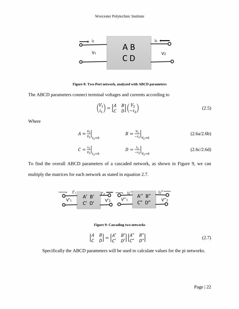
2.5.2 ABCD Parameters
The ABCD parameters are used to analyze a two port network with respect to the total
voltages and currents, as shown in Figure 8. ABCD matrices are mostly used for cascading
networks and to convert to and from different network configurations using the conversion table
provided in Appendix D.
Worcester Polytechnic Institute
Page | 22
A BC D
i1
V1 V2
i2
Figure 8: Two-Port network, analyzed with ABCD parameters
The ABCD parameters connect terminal voltages and currents according to
( ) [
] (
) (2.5)
Where
|
|
(2.6a/2.6b)
|
|
(2.6c/2.6d)
To find the overall ABCD parameters of a cascaded network, as shown in Figure 9, we can
multiply the matrices for each network as stated in equation 2.7.
A’’ B”C” D”
I1'’
V’’1 V’’2A’ B’C’ D’
I’1
V’1 V’2
I’2 I2'’
Figure 9: Cascading two networks
[
] [
] [
] (2.7)
Specifically the ABCD parameters will be used to calculate values for the pi networks.

Worcester Polytechnic Institute
Page | 23
2.6 Even and Odd Mode Analysis
Even and odd mode analysis is a technique used to extract the even and odd-mode
impedances of a circuit. It is employed in horizontally or vertically symmetric circuits. This
technique is based on two principles: symmetry of the circuit and superposition. An example of a
hybrid coupler is shown in Figure 10. The coupler is properly terminated (matched) so that the
reflected power at the input port is zero.
z0
Z01
z0 Z01
Z02 Z02
- +λ/4
λ/4
1
4 3
2
VG
z0 z0
z0 z0
λ/4 λ/4
Figure 10: Quad Hybrid connected with a supply voltage
As shown in Figure 11 the hybrid coupler becomes symmetric when a line splits the
circuit horizontally. The voltage supply is reconfigured to ensure zero voltage at port 4 and VG at
port 1.
QUAD-HYBRID: z0
z0
z0Z01
z0 Z01
Z02 Z02
- +λ/4
λ/4
1
4 3
2- +
- + + -
VG/2VG/2
VG/2 VG/2
z0 z0
z0 z0
Figure 11: Quad-Hybrid symmetrically split

Worcester Polytechnic Institute
Page | 24
For even mode analysis the TL is cut in half and set as an open circuit. This is shown in Figure
12 the voltage supply in port 1 and 2 of the quad hybrid has the same polarity.
z0
z0
z0Z01
z0 Z01
Z02 Z02
λ/4
λ/4
1
4 3
2- +
- +
VG/2
VG/2
z0 z0
z0 z0
λ/8
EVEN:
Figure 12: EVEN mode configuration, open TL
For the odd mode analysis the TL is cut in half and grounded along the symmetry line, as is
shown in Figure 13. The voltage supply of ports 1 and 2 of the quad hybrid has the opposite
polarity. Since the hybrid coupler is a 4 port device, it is analyzed based on the 4x4 matrix
representation of the S-parameters. See section 4 for a more in depth analysis.
z0
z0
z0Z01
z0 Z01
Z02 Z02
λ/4
λ/4
1
4 3
2- +
+ -
VG/2
VG/2
z0 z0
z0 z0
λ/8
ODD:
Figure 13: ODD mode, grounded TL

Worcester Polytechnic Institute
Page | 25
2.7 Network Analyzer Measurements
In the process of developing a new design it is helpful to know how the baseline model
functions. Measurements were planned and executed at the Skyworks Inc. laboratory with a
network analyzer to find the S-Parameters of the existing coupler.
Taking measurements on a network analyzer requires the user to calibrate the system
beforehand. When the measurements for this project were taken at Skyworks, the analyzer was
calibrated using two methods. The first method utilized an automatic electronic calibration. The
second method was to attach a strip of quarter wavelength transmission line between the ports of
the analyzer. A graph of this transmission line (also called thru line) with the electronic
calibration can be seen in Figure 14.
Figure 14: Thru TL using electronic calibration
The difference, as shown by the marker in Figure 14, shows how the transmission line
calibration differed from the electronic calibration. At 1.9 GHz the difference in magnitude was
-.2054dB, which was not a very significant change (two forms of calibration measurements were
taken of the baseline model (Skyworks’ original) of the hybrid coupler.) Throughout the
0 1 2 3 4 5 6 7 8-60
-50
-40
-30
-20
-10
0
10
X: 1.9
Y: -0.2054
Ecal Thru Device 1 S11/21 (dB)
Frequency (GHz)
S-P
aram
eter
Mag
nitu
de (d
B)

Worcester Polytechnic Institute
Page | 26
measurement process a total of four 90 degree hybrid couplers were used to ensure measuring
accuracy.
Figure 15 through Figure 17 were obtained for device 1 using the electronic calibration.
They show the phase and amplitude difference as well as the important S-parameters, S21 and
S31. Because the two calibration types yielded similar results, the graphs using the transmission
line calibration, as well as the graphs for the electronic calibration were omitted but can be found
in Appendix A.
Figure 15: S21 and S31 magnitude using electronic
calibration
Figure 16: Phase difference using electronic calibration
Figure 17: Amplitude difference using electronic calibration
0 1 2 3 4 5 6 7 8-80
-70
-60
-50
-40
-30
-20
-10
0
Frequency (GHz)
S-P
aram
eter
Mag
nitu
de (d
B)
Ecal 90 Degree Hybrid Device 1 S21/31 (dB)
0 1 2 3 4 5 6 7-110
-105
-100
-95
-90
-85
-80
-75
-70
Frequency (GHz)
S-P
aram
eter
Pha
se (d
egre
es)
Ecal 90 Degree Hybrid Device 1 Phase Diff
1.8 1.82 1.84 1.86 1.88 1.9 1.92 1.94 1.96 1.98 2-2
-1.8
-1.6
-1.4
-1.2
-1
-0.8
-0.6
-0.4
-0.2
0
Frequency (GHz)
S-P
aram
eter
Mag
nitu
de (d
B)
Ecal 90 Degree Hybrid Device 1 Amp Diff

Worcester Polytechnic Institute
Page | 27
3 Goal of Project
The goal of this project is to redesign a 90 degree hybrid coupler. The new design needs
to have at least the same electric performance of the current coupler but with an overall smaller
footprint and a larger bandwidth. Using a center frequency of 1.9GHz the goal was to increase
the bandwidth of the target frequency. Once a new model is established a combination of
Advanced Design System (ADS) and High Frequency Structural Simulator (HFSS) software
tools will be used to generate accurate simulations of the circuit. Based on the circuit
simulations, a layout will be created and submitted to our sponsor for tapeout and ultimate
implementation in gallium arsenide. Ultimately, a prototype of the circuit could be produced so
that comparative measurements can be taken on a network analyzer.

Worcester Polytechnic Institute
Page | 28
4 Theoretical Analysis
To determine the characteristic impedances of transmission lines that is used to build the
quad hybrid shown in Figure 10 odd and even mode analysis is applied. As shown in Figure 11-
Figure 13 the quad hybrid is cut in half symmetrically and it is configured for each mode. The
total reflection coefficient at each port is determined by adding the reflection coefficients
(determined from the odd and even modes) using the superposition principle as shown in
equations 4.1a-d. These equations show the relationship between the S-parameters and the
reflected and incident voltages.
[
]
(4.1a)
[
]
(4.1b)
[
]
(4.1c)
[
]
(4.1d)
After the TL in the middle of the hybrid coupler is divided in half it is first set as a short circuit
then it is set as an open circuit. This open and short circuit is represented as a capacitor.
Equation 4.2a represents the capacitive impedance for open circuit in even mode and the
equation 4.2b represents the capacitive impedance for short circuit in odd mode.
z0Z01z0
Z02
λ/4
jBjB
Figure 18: TL stubs

Worcester Polytechnic Institute
Page | 29
(
)
(4.2a)
(
)
(4.2b)
(4.3)
From here the total capacitive impedance can be calculated by using superposition principle by
simply adding the impedances from the odd and even modes as shown in equation 4.3. is the
phase constant and
is the length of the sub section of micro strip line. By building the ABCD
matrix all the stages of the network can be cascaded. Equation 4.4 describes this cascaded
network.
Stub-1 TL (ABCD-parameters) Stub-2
[
] [
] [
]
(4.4)
If the last two matrices are multiplied then the matrix found in equation 4.5 is obtained.
[
] (4.5)
Next, the first matrix of equation 4.4 and equation 4.5 are multiplied to obtain the ABCD
parameters of the network. The final result is given in equation 4.6.
[
] [
( )
] (4.6)
Using the conversion tables, found in Appendix D, and (in terms of ABCD,
characteristic impedance (Z0), and psi ( )) are obtained as shown in equations 4.7a and 4.7b.
(4.7a)
( )
(4.7b)
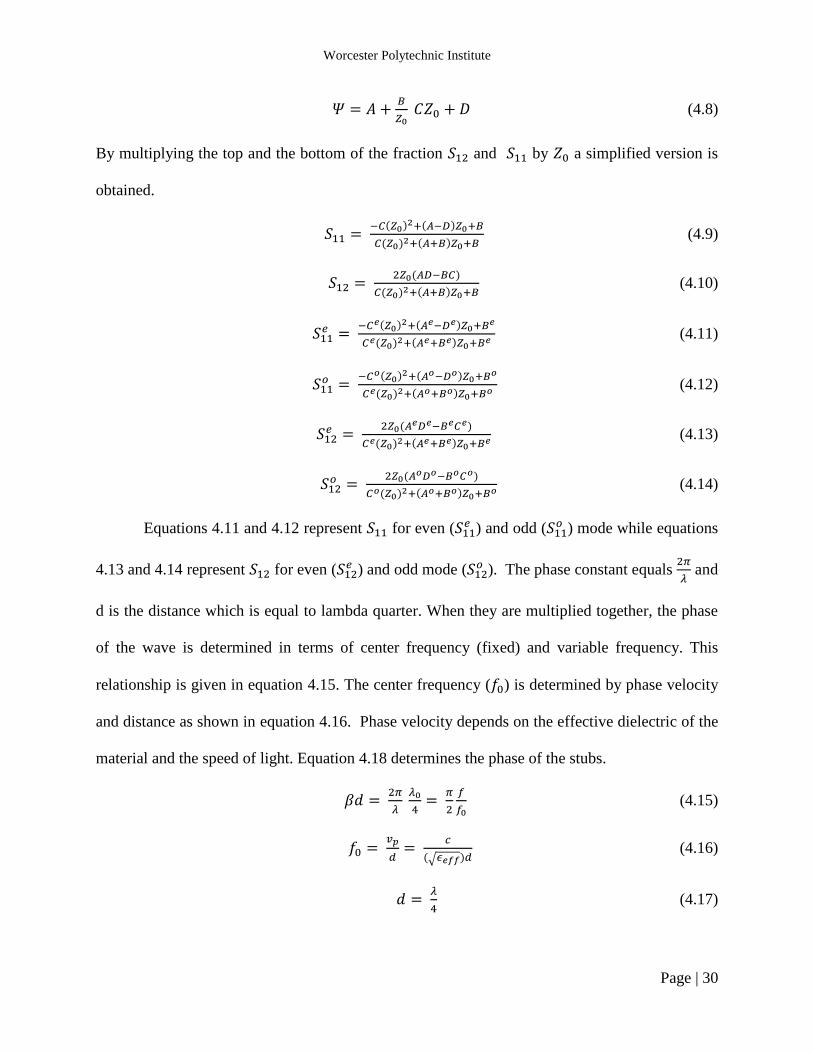
Where psi is in terms of ABCD and Z0 given in equation 4.8.
Worcester Polytechnic Institute
Page | 30
(4.8)
By multiplying the top and the bottom of the fraction and by a simplified version is
obtained.
( )
( )
( ) ( ) (4.9)
( )
( ) ( ) (4.10)
( ) ( )
( ) ( ) (4.11)
( ) ( )
( ) ( ) (4.12)
( )
( ) ( ) (4.13)
( )
( ) ( ) (4.14)
Equations 4.11 and 4.12 represent for even ( ) and odd (
) mode while equations
4.13 and 4.14 represent for even ( ) and odd mode (
). The phase constant equals
and
d is the distance which is equal to lambda quarter. When they are multiplied together, the phase
of the wave is determined in terms of center frequency (fixed) and variable frequency. This
relationship is given in equation 4.15. The center frequency ( ) is determined by phase velocity
and distance as shown in equation 4.16. Phase velocity depends on the effective dielectric of the
material and the speed of light. Equation 4.18 determines the phase of the stubs.
(4.15)
(√ ) (4.16)
(4.17)

Worcester Polytechnic Institute
Page | 31
(4.18)
One special case is when and the 90 degree phase is obtained as shown in equation 4.19.
In equation 4.20 it is shown that tangent equals one which simplifies the equations 4.2a and 4.2b
and the characteristic impedance is determined to be equal to , 50 ohms.
(4.19)
(
) (
) (4.20)
(4.21)
(4.22)
(4.23)
By using the fact that the (
) and the (
) the ABCD matrix of equation 4.6 is
simplified as shown in equation 4.24.
[
] [
( )
] (4.24)
Since the ABCD matrix for even and odd mode can be written as shown in
equations 4.25 and 4.26.
[
] [
( )
] (4.25)
[
] [
( )
] (4.26)
By substituting
,
, and
into the above equations a
simplified version of even and odd ABCD matrix shown in equations 4.27 and 4.28 is derived.
[
] [
] (4.27)

Worcester Polytechnic Institute
Page | 32
[
] [
] (4.28)
Now, by substituting each ABCD parameter from the even mode into the S-parameter even
mode and setting equal to zero, assuming zero reflected power, characteristic impedance
of TL is determined in terms of the characteristic impedance shown in equation 4.30.
( ) ( )
( ) ( ) (4.29)
( ) ( )
(4.29a)
(
)( )
(
) (4.29b)
( )
(4.29c)
( ) ( )
(4.29d)
( ) ( )
(4.29e)
( ) ( )
(4.29f)
The magnitude of the impedances in equation 4.29 determines the characteristic impedance in
equation 4.30.
√ (4.30)
In the odd mode was set to zero and the same result was obtained. By deriving the
characteristic impedances, each transmission line can be designed using the equations of
microstrip transmission lines. The other S-parameters are computed using ,
, ,
which are previously defined as shown in equations 4.31 to 4.35.
(4.31)
(4.32)

Worcester Polytechnic Institute
Page | 33
(4.33)
(4.34)
(4.35)

Worcester Polytechnic Institute
Page | 34
5 New design approach
The analytical analysis determined the characteristic impedances of the TLs are shown in
Figure 19. This led to the design of the microstrip line to determine the length, width, and height
by assuming an infinitesimal TL thickness.
PORT_1
PORT_3PORT_4
PORT_2
T2A
T1A
T1B
T2B
d1=λ1/4
d2=λ2/4
Figure 19: The new design quad hybrid
(5.1a)
(5.1b)
(5.1c)
(5.1d)
(√ ) (5.2a)
(√ ) (5.2b)
√

Worcester Polytechnic Institute
Page | 35
The characteristic impedance of the transmission T1A is . Characteristic impedance
was decided to be set to 50 ohm because this value is the most commonly used in industry.
For this process the dielectric constant was set to be . Next, to determine the distance (d)
in equation 5.2 the effective dielectric has to be computed using equation 5.3. This equation
depends on the height to width ratio which is determined using the graph in Figure 20. The lines
are drawn for different values of dielectric constants, in this case 6 is used. As shown in the
graph, the width to height ratio is less than 2, this condition determines that the equation 5.3 is
used to compute this ratio.
[(
)
(
)
] (5.3)
, √
, ,
(5.4a/b/c/d)
Figure 20: Microstrip Z0 as function of w/h (Z02)
(5.5)

Worcester Polytechnic Institute
Page | 36
In order to solve for the width and height of the second transmission line (T2A &T2B)
the factor A must be determined first. This is accomplished by substituting the dielectric
constant, effective impedance, and characteristic impedance. The factor A was calculated using
equation 5.6.
√
(
) (5.6)
The final results for these transmission lines are shown in equation 5.7.
A = 1.737215,
, , (5.7a/b/c/d)
The effective dielectric constant of second TL is determined by substituting the dielectric
constant and the height to width ratio to equation 5.5. By using the equation 5.2 the length of TL
is calculated. The results are shown below in equation 5.8.
(5.8a/b/c)
To determine the width to height ratio of the first TL (T1A & T1B) the same procedure is
followed. As shown in Figure 21, the approximate value of width to height is determined and
since this ratio is greater than two, equation 5.10 is used to compute it.
, √
,
√
√ ,
(5.9a/b/c/d)

Worcester Polytechnic Institute
Page | 37
Figure 21: Microstrip Z0 as function of w/h (Z01)
The equation below computes the width to height ratio, but first the B factor in equation 5.11 is
calculated and substituted into this formula.
( )
[ ( )
] (5.10)
√ (5.11)
(5.12)
After the height to width ratio was computed the effective dielectric constant was calculated
next. This value and the center frequency are used to compute the length of the TL.
(5.13)
All these values lead to a new design which was implemented in ADS as shown in Figure 22.
Worcester Polytechnic Institute
Page | 38
PORT_1
PORT_3PORT_4
PORT_2
T2A
T1A
T1B
T2B
d1=λ/4 = 7.3925 cm
d2=λ2/4= 7.58478 cm
Z2 = 50 Ω
Z1 = 35.35 Ω
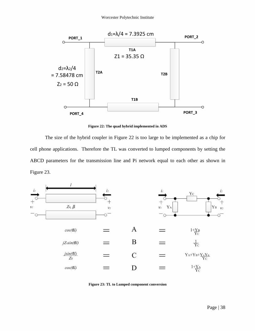
Figure 22: The quad hybrid implemented in ADS
The size of the hybrid coupler in Figure 22 is too large to be implemented as a chip for
cell phone applications. Therefore the TL was converted to lumped components by setting the
ABCD parameters for the transmission line and Pi network equal to each other as shown in
Figure 23.
Figure 23: TL to Lumped component conversion
Worcester Polytechnic Institute
Page | 39
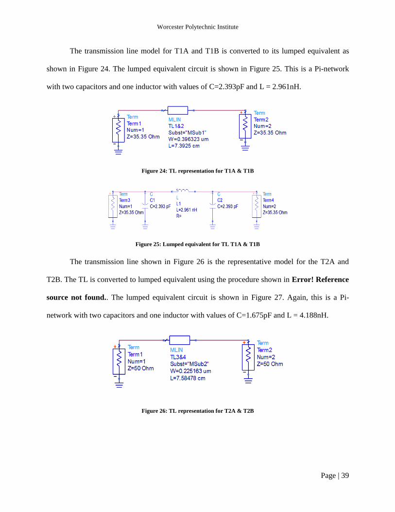
The transmission line model for T1A and T1B is converted to its lumped equivalent as
shown in Figure 24. The lumped equivalent circuit is shown in Figure 25. This is a Pi-network
with two capacitors and one inductor with values of C=2.393pF and L = 2.961nH.
Figure 24: TL representation for T1A & T1B
Figure 25: Lumped equivalent for TL T1A & T1B
The transmission line shown in Figure 26 is the representative model for the T2A and
T2B. The TL is converted to lumped equivalent using the procedure shown in Error! Reference
source not found.. The lumped equivalent circuit is shown in Figure 27. Again, this is a Pi-
network with two capacitors and one inductor with values of C=1.675pF and L = 4.188nH.
Figure 26: TL representation for T2A & T2B

Worcester Polytechnic Institute
Page | 40
Figure 27: Lumped equivalent for TL T2A & T2B
After the conversion has been done all the Pi-networks are connected together to obtain the
circuit shown in Figure 28. This circuit is simplified by combining the parallel corner capacitors.
Figure 28: The lumped equivalent circuit of the quad hybrid
The simplified model of the lumped equivalent is shown in Figure 29. This model can be
implemented as a chip because its size is smaller and the output results show a greater bandwidth
for the 90 degree phase and the 3 dB attenuation at the output ports.

Worcester Polytechnic Institute
Page | 41
Figure 29: Final Lumped equivalent circuit

Worcester Polytechnic Institute
Page | 42
6 Simulations
6.1 Simulation and data analysis tools
There are many tools used for analysis including HFSS, ADS, and Matlab. These
programs provide the necessary tools that enable models to be generated and simulations to be
run on a wide variety of applications.
6.1.1 High Frequency Structural Simulator (HFSS)
“ANSYS HFSS software is the industry-standard simulation tool for 3-D full-wave
electromagnetic field simulation and is essential for the design of high-frequency and high-speed
component design.” [9] It has the ability to utilize either the finite element method (FEM) or the
integral equation method to generate meshes as a way of approximating solutions of partial
differential equations.
Among its capabilities, is the ability to plot electromagnetic fields (both in the near and
far field), many different parameters (S, Z, ABCD), and radiation patterns. HFSS also shares the
same mother company (ANSYS) as SolidWorks and is very similar in its modeling capabilities.
The ability to import designs from SolidWorks as well as export solutions to a wide variety of
programs makes it very versatile. Overall, it is an extremely useful program that provides a lot
of pertinent and usable data for high frequency applications.
6.1.2 Advanced Design Systems (ADS)
Another circuit modeler is ADS. ADS is a circuit simulator with abilities ranging from
simulation of simple circuits to the ability of arranging complex layouts with many different
layers. A great feature found in ADS is the 2.5-D simulator called momentum. Once a layout is
created, momentum is used to simulate the design’s performance almost like it would on a real

Worcester Polytechnic Institute
Page | 43
die, with the exception of accounting for parasitics. Like HFSS it also uses finite element
method to generate meshes and solve circuits.
Solutions from ADS range from simple parameter plots to smith charts and has proven to
be another industry standard.
6.1.3 Matlab
Matlab is a mathematical program useful in all sorts of computational analyses.
Moreover it “is a high-level language and interactive environment for numerical computation,
visualization, and programming.” [10] It can analyze data, plot charts, run programs written in a
C based language and do almost anything else mathematical. Algorithms can be generated and
specific functions created, and data can be imported and analyzed.
Worcester Polytechnic Institute
Page | 44
7 Computational Analysis
7.1 ADS Simulations
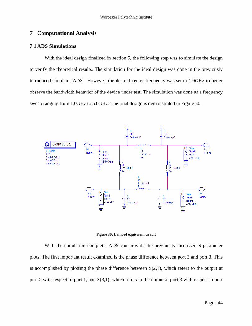
With the ideal design finalized in section 5, the following step was to simulate the design
to verify the theoretical results. The simulation for the ideal design was done in the previously
introduced simulator ADS. However, the desired center frequency was set to 1.9GHz to better
observe the bandwidth behavior of the device under test. The simulation was done as a frequency
sweep ranging from 1.0GHz to 5.0GHz. The final design is demonstrated in Figure 30.
Figure 30: Lumped equivalent circuit
With the simulation complete, ADS can provide the previously discussed S-parameter
plots. The first important result examined is the phase difference between port 2 and port 3. This
is accomplished by plotting the phase difference between S(2,1), which refers to the output at
port 2 with respect to port 1, and S(3,1), which refers to the output at port 3 with respect to port

Worcester Polytechnic Institute
Page | 45
1. The result of this phase difference is shown in Figure 31 where the plot shows degrees vs.
frequency. The plot shows that the 90 degree phase difference is maintained for range of 0.4GHz
Figure 31: The phase difference of two output ports
Next, the magnitude of the output signal is examined. As previously discussed, half of the
power should be observed at port 3 and port 2. This is done by simply plotting the results S(2,1)
and S(3,1).
In Figure 32 the results are shown in terms of magnitude (dB) versus frequency. The plot
shows the 3dB attenuation, or half of the power, of the output ports and these are maintained for
the same range of frequencies.

Worcester Polytechnic Institute
Page | 46
Figure 32: The 3dB attenuation of the two output ports
The 90 degree phase difference and 3dB attenuation are maintained for 0.4GHz. To
calculate for the bandwidth we use the equation:
(7.1)
Where fu refers to the upper limit for which the system is functional (in this case 2.111GHz), fl is
the lower limit (in this case 1.757GHz), and finally fc was the initially determined center
frequency of 1.9GHz. Inserting these values into the equation yields a bandwidth of 18.42%.
These results confirm the theoretical analysis, in addition to accomplishing one of the project
goals.
7.2 Capacitor and spiral inductor calculations
For the schematic in Figure 29 the capacitors and spiral inductors needed to be calculated
so that their physical parameters are determined.
In order to find the values for the capacitor of 4.068pF the parallel plate capacitor
equation was used [11].

Worcester Polytechnic Institute
Page | 47
(7.2)
In equation 7.2, C is the capacitance, is the permittivity of free space (8.85E-12), is the
relative dielectric constant, A is the area of the plates, and d is the distance between the parallel
plates. The relative dielectric constant depends completely upon the material, in the case of this
new circuit the relative dielectric was set to 6. Plugging in all of the known values (capacitance,
permittivity, dielectric) the only variables left are the area, A, and the distance, d. In an effort to
reduce the total area, the equation above can be analyzed to see that the smallest d would
minimize the area. Next, according to the layout process used by Skyworks (PHEMT7), the
thinnest layer that can be made is one of 0.15um. Using this value for d the one variable
remaining is A.
( )( )
( )( ) (7.3)
√ (7.4)
After the area is found in equation 7.3, the square root is taken so that the dimensions of the caps
are found in equation 7.4 to be 104um.
Next, the spiral inductors’ dimensions were calculated for the values of 4.188nH and
2.961nH. There are three main spiral inductor equations. They are the Modified Wheeler,
Current Sheet, and the Monomial Fit [12]. They all have their different merits and usually yield
similar results. For these calculations an integrated spiral inductor calculator from Stanford
University was used which required some starting values to be known [13]. These values
included the number of turns (n), turn spacing (s), turn width (w), and the outer diameter (dout).
According to Skywoks’ PHEMT7 process the turn spacing and width has certain minimum
values that are set in place. In this case the minimum is 6um for both. Instead of choosing the
minimum the values, the turn width and the turn spacing were both set to 10um. With regards to

Worcester Polytechnic Institute
Page | 48
the outer diameter, the goal of reducing the total size of the circuit was considered, and because
of this the diameter was estimated to be at 300um. The rest was experimenting with the number
of turns to see what the optimal number was to obtain the inductance values of 4.188nH and
2.961nH. In order to reduce the total number of spiral inductors on the board, which would have
been four, two inductor values were combined into a single one, resulting in a total of two. Then
a line feeding into the inductor would split it in two and work in the same way. After tuning the
amount of turns to get the desired result it was found that the ideal number was approximately
six.
The calculated spiral inductor values, as well as the capacitor values were then utilized in
sections 7.3 and 7.4 in order to complete the 3D model.
7.3 Step By Step ADS Layout
This section provides step by step instructions to create the layout for the new design that
was discussed in the previous sections. The program used in this section is Agilent’s ADS which
was also introduced in previous sections for simple 2-D schematics. This section makes use of
ADS’ layout functionality as well as a 2.5D simulator momentum.
Step 1: The first step is to start the ADS working environment.
Figure 33: Start Agilent's Advanced Design System

Worcester Polytechnic Institute
Page | 49
Step 2: Once the program fully opens, the first thing to do is create a workspace, where the
design will be implemented. To do so, click on File>New>Workspace as is shown in the figure
below.
Figure 34: Create a new workspace
Worcester Polytechnic Institute
Page | 50
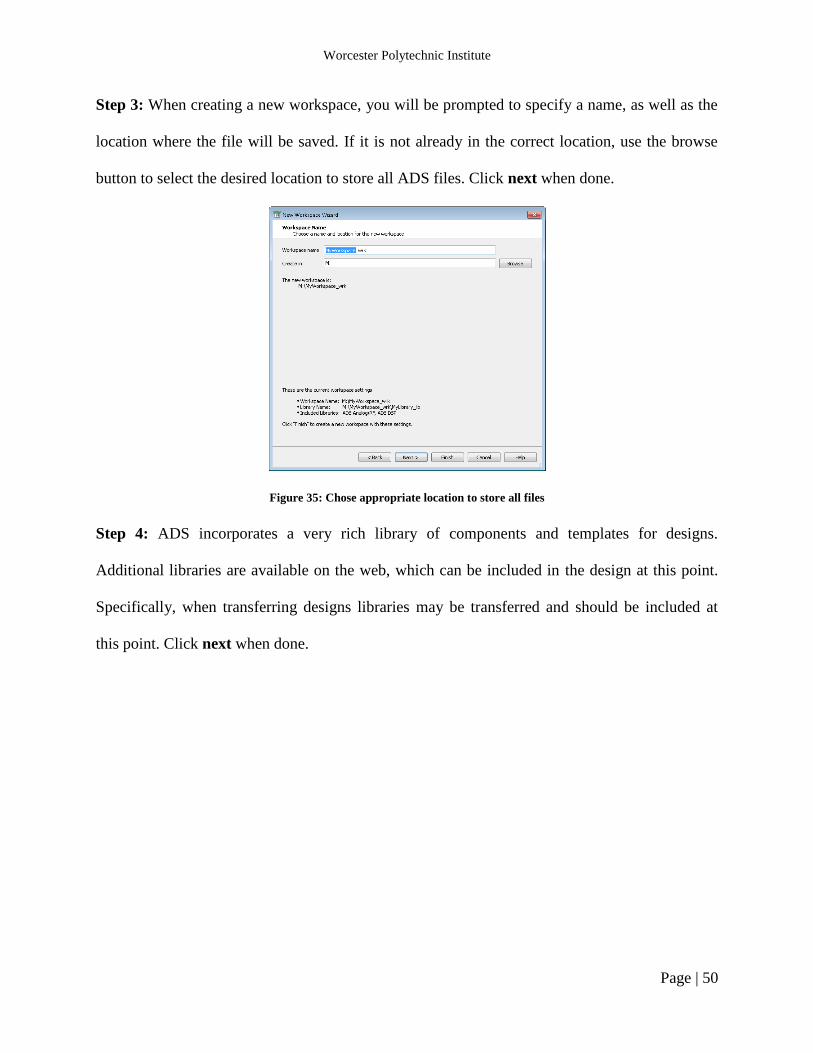
Step 3: When creating a new workspace, you will be prompted to specify a name, as well as the
location where the file will be saved. If it is not already in the correct location, use the browse
button to select the desired location to store all ADS files. Click next when done.
Figure 35: Chose appropriate location to store all files
Step 4: ADS incorporates a very rich library of components and templates for designs.
Additional libraries are available on the web, which can be included in the design at this point.
Specifically, when transferring designs libraries may be transferred and should be included at
this point. Click next when done.

Worcester Polytechnic Institute
Page | 51
Figure 36: Select the desired libraries
Step 5: ADS stores all designs under libraries. It is important to name the library accordingly to
the specific design for ease of later use. This will become important later. Click next to proceed.
Figure 37: Create your own library

Worcester Polytechnic Institute
Page | 52
Step 6: In this window, the units are specified for all schematics/layouts created in this
workspace. Choose the units of your best liking and click finished when done. For this design,
microns were the unit of preference as shown below.
Figure 38: Select default units
Step 7: A new window similar to that of the one on startup will appear with the exception that
this will be empty since nothing has been created yet. Go to File>New>Layout where you will
be prompted to name the layout. A new window will open like the one shown below.

Worcester Polytechnic Institute
Page | 53
Figure 39: Starting new layout
Step 8: The ADS layout environment works with a systems of layers. Each layer can be
considered as conducting metals. Before proceeding, go to Options>Technology>Layer
Properties and the window shown in Figure 40. Click Add Layer.
Figure 40: Creating layers

Worcester Polytechnic Institute
Page | 54
Step 9: The window shown in Figure 41 will appear where the user is prompted to specify the
name of a layer along with a variety of different parameters. Each component in the design needs
to be different layers (i.e. ports, inductors, capacitors). Specify the name and properties of the
layers and press ok when finished. Then select ok again in the previous window. Again, it is
important to note that each conductor will need to be mapped as a layer so make sure all the
required conductors from the design are specified.
Figure 41: Layer properties

Worcester Polytechnic Institute
Page | 55
Step 10: It is good practice to specify different colors, transparency and patterns to all the layers.
This will be useful especially when creating complex designs, since it will help tell the
conducting layers apart one from another. Also, it makes it easy for the designer to follow the
design through since no design is created in a single attempt. By going to Options > Layer
Preferences the window shown in Figure 42 will appear. This shows all the layers that have
been defined along with their properties, where the designer can change the preferences of each
layer at will.
Figure 42: Layer preferences window

Worcester Polytechnic Institute
Page | 56
Step 11: ADS features a variety of ways to implement a design including a respectable library of
components. However, since most printed board designs require custom components this tutorial
shows how to design the component using traces. To begin use the “insert path” tool available
from the toolbars. Alternatively, it the tool is under Insert>Path. To use this tool, click the
cursor to set the starting point of the trace. Then, wherever the cursor is moved the trace will
follow. After the starting point is specified, the cursor indicates the x and y displacement from
that point. You can also specify the width of the trace, whether the turns should be a curve, or
squared in the popup window. This is all shown in Figure 43 below.
Figure 43: Insert path

Worcester Polytechnic Institute
Page | 57
Step 12: Create the spiral inductor by creating several turns clicking to indicate every corner.
When the final point is reached, simply click twice over the same point to finish the trace. The
finalized inductor is shown in Figure 44, where the design of the inductor was determined from
the previous sections. When the path has been completed, double click anywhere on the path to
get the window shown below. In this window, specify the correct layer for the path. For this
design this inductor will be the inductor located at the top of the chip so it belongs to the layer
Inductor_Top. The design of this inductor has been previously discussed, which implements two
separate inductors required by the design. By using one large spiral inductor and splitting it at a
point in between the end points a value of an inductor is obtained, while a connection at the end
point of the spiral creates a separate inductor with a different value hence implementing two
inductors with a single spiral.

Worcester Polytechnic Institute
Page | 58
Figure 44: Creating an inductor
Step 13: The capacitors for this circuit will be implemented by using two parallel plates
separated over a later specified distance. First the top plate of the capacitor is created using the
“Insert Rectangle” tool found again in the toolbars or alternative under Insert>Rectangle.
Similar to the path, click to indicate the starting point of the rectangle and move the cursor until
the right dimensions display on the screen. The dimensions can always be changed through the
window shown in Figure 45 which is accessed by double clicking on the layer. Again, remember
to specify the correct layer for the top of the capacitor. In this circuit this layer is assigned the
name Cap_Top.

Worcester Polytechnic Institute
Page | 59
Figure 45: Creating the top plate of the capacitor

Worcester Polytechnic Institute
Page | 60
Step 14: All the capacitors for this circuit are identical, therefore instead of repeating the
previous step three additional times, simply select the capacitor layer. Copy the layer by either
pressing CTRL+C or selecting copy from the right mouse click menu. Paste the layer pressing
CTRL+V or again using the right mouse click and position each layer where desired. The four
top layers have now been created and are shown in Figure 46.
Figure 46: Top plates for capacitors

Worcester Polytechnic Institute
Page | 61
Step 15: Next, using again the insert rectangle tool create a rectangle that will be used for the
ports of the device. Once the rectangle has been created assign the rectangle to the correct layer.
In this design they were assigned to the Ports layer as shown in Figure 47. Again, copy the
rectangle shape in the same manner described in the previous step and place three additional
ones for a total of four ports similar to the layout shown in Figure 47.
Figure 47: Input pads

Worcester Polytechnic Institute
Page | 62
Step 16: Next, the bottom plate of the capacitor is created. This is easily done by selecting the
four already drawn shapes for the capacitors, copying them, and pasting them into place. Double
click on the already selected shapes, and assign the shapes to the correct layer. In this circuit,
they were assigned to the layer called Cap_Bot. This is shown in Figure 48 where the layer
Cap_top has been altered to make it more transparent in order to see what is behind the layer.
Figure 48: Bottom capacitors

Worcester Polytechnic Institute
Page | 63
Step 17: To change the transparency of a layer, go to the Layers Preferences window available
from Options>Layer Preferences and find the name of the layer that needs to be altered. The
name is displayed in the left-most column in Figure 49. Once the layer is found, double click on
the column labeled “Trans” (second from the right in the figure below), and new window pops
up as shown below. Adjust the slider until satisfied and press ok to continue. The selected layer’s
transparency should now have changed, and should be noticed in the layout window.
Figure 49: Changing the transparency

Worcester Polytechnic Institute
Page | 64
Step 18: Symmetry also applies to the inductors of this circuit, therefore to create the bottom
inductor simply copy and place it right on the same position as the other. Once the new inductor
is placed, assign it to the correct layer as was done with the previous shapes. The bottom
inductor was placed in a layer called Inductor_Bot. See Figure 50 for the expected resulting
view.
Figure 50: Bottom inductor

Worcester Polytechnic Institute
Page | 65
Step 19: Next, create the bottom part of the ports. This will act as the common ground, where
everything in the circuit will connect to complete the loop. This is simply done by copying the
already created layers and placing them in the same place. After placed, select them and assign
them to the correct layers as shown in Figure 51. In this picture, the colors of the previous ports
appear to have changed. This occurs because the layer that is currently assigned to the bottom
part of the port has a higher hierarchy. However, this drawing does not determine the order of the
layers but only their general “print” area or the general area where the specified layer should
exist. The physical orientation of the layers will be done in later steps, however if this is cause
for confusion of the designer the layer hierarchy can be changed by going into the Layer
Definitions menu from the Options>Technology>Layer Definitions.
Figure 51: Bottom of the port connectors
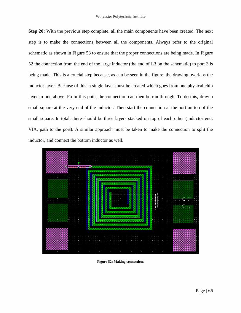
Worcester Polytechnic Institute
Page | 66
Step 20: With the previous step complete, all the main components have been created. The next
step is to make the connections between all the components. Always refer to the original
schematic as shown in Figure 53 to ensure that the proper connections are being made. In Figure
52 the connection from the end of the large inductor (the end of L3 on the schematic) to port 3 is
being made. This is a crucial step because, as can be seen in the figure, the drawing overlaps the
inductor layer. Because of this, a single layer must be created which goes from one physical chip
layer to one above. From this point the connection can then be run through. To do this, draw a
small square at the very end of the inductor. Then start the connection at the port on top of the
small square. In total, there should be three layers stacked on top of each other (Inductor end,
VIA, path to the port). A similar approach must be taken to make the connection to split the
inductor, and connect the bottom inductor as well.
Figure 52: Making connections

Worcester Polytechnic Institute
Page | 67
Figure 53: Schematic reference
Step 21: The finalized design is shown in Figure 54. In this design, the layer properties for each
component were progressively modified as each connection was implemented in order to easily
tell apart all the different layers through different colors. Notice the different colors going from
the inductors to the rest of the circuit, the different VIAs and conducting layers are shown in
different colors. Once all the proper connections are complete, the last step is to insert the actual
ports. To do so, click the insert Pin icon, or Insert>Pin and click on the previously placed ports
accordingly. The pins will also need to be placed on the right layer so double click on the pin and
assign it to the correct layer.
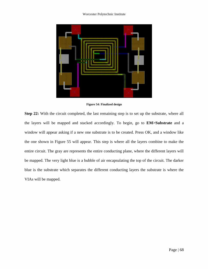
Worcester Polytechnic Institute
Page | 68
Figure 54: Finalized design
Step 22: With the circuit completed, the last remaining step is to set up the substrate, where all
the layers will be mapped and stacked accordingly. To begin, go to EM>Substrate and a
window will appear asking if a new one substrate is to be created. Press OK, and a window like
the one shown in Figure 55 will appear. This step is where all the layers combine to make the
entire circuit. The gray are represents the entire conducting plane, where the different layers will
be mapped. The very light blue is a bubble of air encapsulating the top of the circuit. The darker
blue is the substrate which separates the different conducting layers the substrate is where the
VIAs will be mapped.

Worcester Polytechnic Institute
Page | 69
Figure 55: Substrate setup

Worcester Polytechnic Institute
Page | 70
Step 23: To insert a conducting layer right click on the gray area and select “Map Conductor
Layer”. The window will prompt for properties of the conductor layer. First, specify the layer
that needs to be placed, in this example first the top inductor is placed. The material of the
inductor can be specified, but those parameters depend strictly on the manufacturing process. For
this tutorial, it was left as a perfect conductor. Lastly, the thickness of the layer can be specified
which here was set to 10 microns. The next step is to keep stacking the layers.
Figure 56: Inserting a conducting layer

Worcester Polytechnic Institute
Page | 71
Step 24: To keep adding layers on top, right click on the substrate (darker blue) and select
“Insert Substrate Layer Above” or below. Different layers can be mapped on top/below or on the
side of the already mapped conductor layers. Not that by clicking on the substrate, the material of
the substrate can be modified as well as the thickness of the substrate. Change these to match the
design requirements. Add all the conducting layers now and make sure to use each layer as
much as possible. Note that the VIAs are mapped differently and are discussed on the next step.
Figure 57: Inserting layers above/below

Worcester Polytechnic Institute
Page | 72
Step 25: To insert a VIA connecting different layers, right click on the substrate and click “Map
Conductor VIA.” Similar to the previous conductors, select a layer to assign to the VIA. In
Figure 58 the layer jumper connects the inductor to the layer that connects the inductor to the
capacitors and the ports, called Cap_Ind. Since the Cap_Ind is on the same layer as the Ports,
wherever they overlap in the original layout drawing window will indicate that they are
connected. Repeat this procedure until the entire circuit is mapped and ready to function.
Figure 58: Inserting conductor VIA
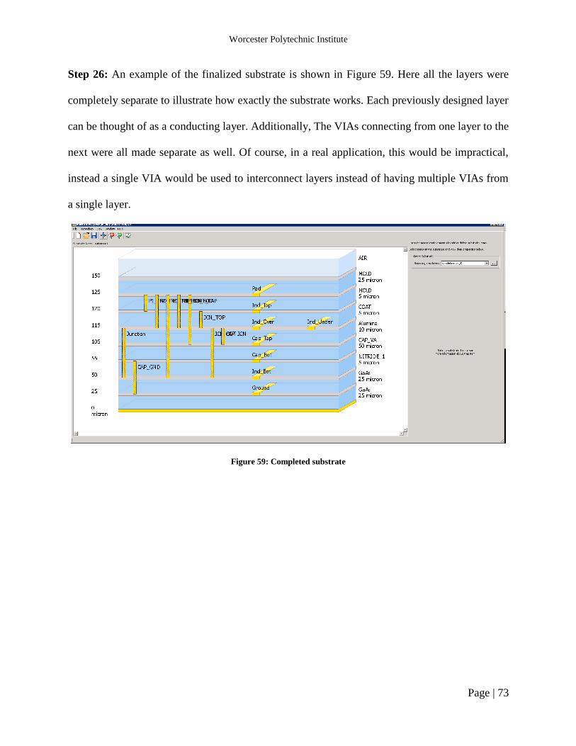
Worcester Polytechnic Institute
Page | 73
Step 26: An example of the finalized substrate is shown in Figure 59. Here all the layers were
completely separate to illustrate how exactly the substrate works. Each previously designed layer
can be thought of as a conducting layer. Additionally, The VIAs connecting from one layer to the
next were all made separate as well. Of course, in a real application, this would be impractical,
instead a single VIA would be used to interconnect layers instead of having multiple VIAs from
a single layer.
Figure 59: Completed substrate

Worcester Polytechnic Institute
Page | 74
Step 27: Once the substrate has been completed, a 3D model of the design can be seen by going
to EM>3D EM Preview an example of which is shown in Figure 60. It is important to note that
ADS will not simulate in a 3D environment, it will only display a model of the design. This 3D
modeling tool is a good way to ensure that the desired circuit has been implemented, where all
the VIAs and layers are shown for full inspection. The 3D EM Preview combines the drawings
from the Layout window and the substrate setup to generate the mode.
Figure 60: 3-D Model
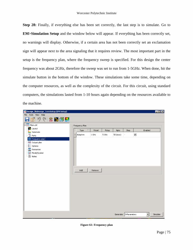
Worcester Polytechnic Institute
Page | 75
Step 28: Finally, if everything else has been set correctly, the last step is to simulate. Go to
EM>Simulation Setup and the window below will appear. If everything has been correctly set,
no warnings will display. Otherwise, if a certain area has not been correctly set an exclamation
sign will appear next to the area signaling that it requires review. The most important part in the
setup is the frequency plan, where the frequency sweep is specified. For this design the center
frequency was about 2GHz, therefore the sweep was set to run from 1-5GHz. When done, hit the
simulate button in the bottom of the window. These simulations take some time, depending on
the computer resources, as well as the complexity of the circuit. For this circuit, using standard
computers, the simulations lasted from 1-10 hours again depending on the resources available to
the machine.
Figure 61: Frequency plan
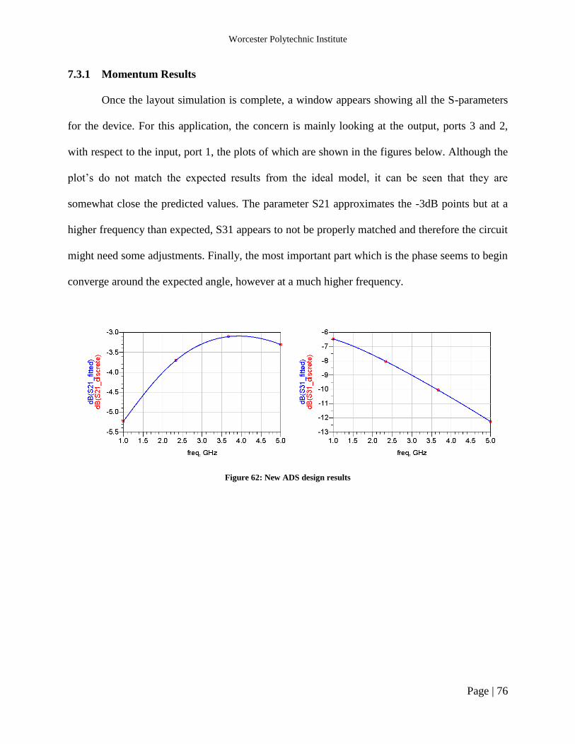
Worcester Polytechnic Institute
Page | 76
7.3.1 Momentum Results
Once the layout simulation is complete, a window appears showing all the S-parameters
for the device. For this application, the concern is mainly looking at the output, ports 3 and 2,
with respect to the input, port 1, the plots of which are shown in the figures below. Although the
plot’s do not match the expected results from the ideal model, it can be seen that they are
somewhat close the predicted values. The parameter S21 approximates the -3dB points but at a
higher frequency than expected, S31 appears to not be properly matched and therefore the circuit
might need some adjustments. Finally, the most important part which is the phase seems to begin
converge around the expected angle, however at a much higher frequency.
Figure 62: New ADS design results
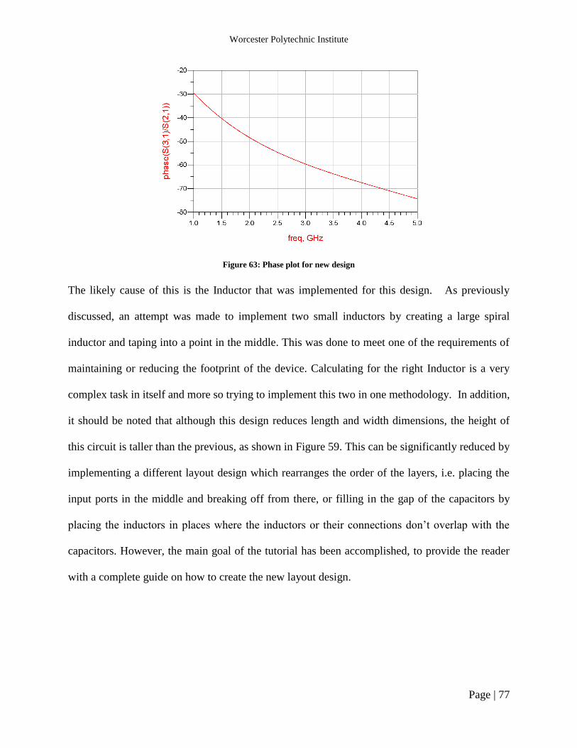
Worcester Polytechnic Institute
Page | 77
Figure 63: Phase plot for new design
The likely cause of this is the Inductor that was implemented for this design. As previously
discussed, an attempt was made to implement two small inductors by creating a large spiral
inductor and taping into a point in the middle. This was done to meet one of the requirements of
maintaining or reducing the footprint of the device. Calculating for the right Inductor is a very
complex task in itself and more so trying to implement this two in one methodology. In addition,
it should be noted that although this design reduces length and width dimensions, the height of
this circuit is taller than the previous, as shown in Figure 59. This can be significantly reduced by
implementing a different layout design which rearranges the order of the layers, i.e. placing the
input ports in the middle and breaking off from there, or filling in the gap of the capacitors by
placing the inductors in places where the inductors or their connections don’t overlap with the
capacitors. However, the main goal of the tutorial has been accomplished, to provide the reader
with a complete guide on how to create the new layout design.

Worcester Polytechnic Institute
Page | 78
7.4 Step by step layout instructions for HFSS
When starting a new model in HFSS the most important part is to have a visualization of
the design to have a better idea of how to approach the design. For the new design-approach a
lumped equivalent model was produced, as shown in Figure 29. In this case the best place to
start would be with the spiral inductors, which will both take up the most space of the layout as
well as be the best point to base our variables off of. Do not forget to save periodically!
Step 1: After opening up HFSS 14.0 click on the menu project followed by what should be the
first choice in the menu, Insert HFSS Design.
Step 2: Select draw line in the shortcut menu and draw a random spiral inductor. It does not
matter at this point what exactly it looks like so long as the exact number of turns that you want
to have in the inductor are there. The inductor that is being created is going to be six turns.
When finished right click the screen and select done.

Worcester Polytechnic Institute
Page | 79
Figure 64: Drawing the spiral inductor
Step 3: Now in the object tree expand Lines>Polyline 1>Createpolyline until all of the create
lines are shown. Next double click the first line and set the position in the form of a variable so
that in the future it can be easily modified. Some good starting coordinates would be [-
spiral_diam/2 ,spiral_diam/2 ,0um]. Continuing on the last line, taking into account the spacing
between the spirals and the width of the spirals, can be summed up using the coordinates [(-
spiral_diam/2+6*(spiral_width+spiral_spacing)),-1*(spiral_diam/2+5*(spiral_width
+spiral_spacing)) ,0um]. The rest of these points can be extrapolated using these coordinates.
The starting variables should be 400um for spiral diameter, 10um for spiral spacing, and 10um
for spiral width.
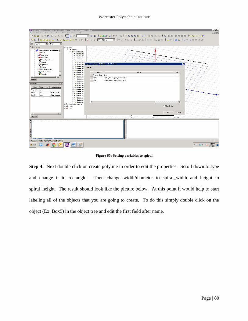
Worcester Polytechnic Institute
Page | 80
Figure 65: Setting variables to spiral
Step 4: Next double click on create polyline in order to edit the properties. Scroll down to type
and change it to rectangle. Then change width/diameter to spiral_width and height to
spiral_height. The result should look like the picture below. At this point it would help to start
labeling all of the objects that you are going to create. To do this simply double click on the
object (Ex. Box5) in the object tree and edit the first field after name.

Worcester Polytechnic Institute
Page | 81
Figure 66: Spiral inductor
Step 5: Now select the spiral inductor that was just made and copy and then paste it. Now it is
needed to put them on different layers so go up to
Modeler>CoordinateSystem>Create>RelativeCS>Offset and create an offset coordinate
system of desired distance. Next go to the properties of the second spiral inductor and select the
new coordinate system. The next thing that should be done is to right click on the second spiral,
go to Edit>Arrange>Rotate and rotate it 180 degrees around the z axis. It should now look like
it does below. If the spirals are reversed then in the object tree you have to right-click on them
and mirror them under Edit>Arrange->Mirror option.

Worcester Polytechnic Institute
Page | 82
Figure 67: Double spirals
Step 6: Next the bondpads and the capacitors will be created. To start off create a new
coordinate system, which will be for the capacitors and bondpads, with the starting point at [0um
,0um ,-spiral_space/2]. Refer to step 5 if help is needed creating one.
Next create two random boxes outside of the spiral inductors. Again, it does not matter
what they look like, that will soon be corrected. Also, make sure that the cap and bondpad
coordinate system is selected. For a general reference as to where to put them look at Figure 69.
Now the difficult part is to get them into the correct position. For the bondpad (orange box) set
the starting point at [-bondcap_space/2 ,-spiral_diam/2-cap_size-space_bondcap ,0um] and the
xsize equal to –padsize, ysize equal to padsize, and zsize equal to 3um. Padsize, using the
PHEMT7 process, can be estimated at 78um. Now, the parallel plate capacitor will be made out
of the box drawn, which will act as the top plate. Edit that box and make the starting point [-

Worcester Polytechnic Institute
Page | 83
(spiral_diam/2)-40.5um ,-(spiral_diam/2)-cap_spiral_space ,cap_via/2, the xsize cap_size, ysize -
cap_size, and zsize 2um]. Cap_size was found in section 7.2 and can be rounded to 105um.
Cap_via will be utilized soon but for now can be set to .15um. Now click on the top plate of the
capacitor and copy and paste it one time. The second box will appear in the object tree to the
left. Edit the bottom plate’s (the copied box) starting point to be [-(spiral_diam/2)-40.5um ,-
(spiral_diam/2)-cap_spiral_space ,-cap_via/2] and zsize to be -2um. There should now be two
parallel plates on the screen. Next, make the cap_via by creating a box in between both of the
plates. The starting point for the via should be [-(spiral_diam/2)-40.5um ,-(spiral_diam/2)-
cap_spiral_space ,-cap_via/2], with xsize equal to cap_size, ysize equal to –cap_size, and zsize
equal to cap_via.
Figure 68: Capacitor and bondpad after correction
The circuit should now look like it does in the above picture. Now, in order to make the
three other bondpads and capacitors do the following. First select and copy the first bondpad and
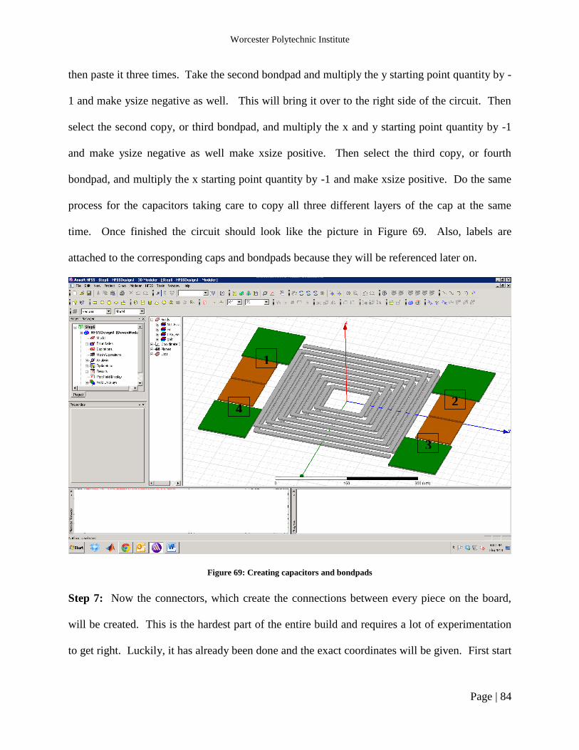
Worcester Polytechnic Institute
Page | 84
then paste it three times. Take the second bondpad and multiply the y starting point quantity by -
1 and make ysize negative as well. This will bring it over to the right side of the circuit. Then
select the second copy, or third bondpad, and multiply the x and y starting point quantity by -1
and make ysize negative as well make xsize positive. Then select the third copy, or fourth
bondpad, and multiply the x starting point quantity by -1 and make xsize positive. Do the same
process for the capacitors taking care to copy all three different layers of the cap at the same
time. Once finished the circuit should look like the picture in Figure 69. Also, labels are
attached to the corresponding caps and bondpads because they will be referenced later on.
Figure 69: Creating capacitors and bondpads
Step 7: Now the connectors, which create the connections between every piece on the board,
will be created. This is the hardest part of the entire build and requires a lot of experimentation
to get right. Luckily, it has already been done and the exact coordinates will be given. First start
1
4 2
3

Worcester Polytechnic Institute
Page | 85
by making a box at the inner point of the spiral inductor, these boxes are so they do not intersect
with any unwanted parts. It has a starting point of [-
spiral_diam/2+6*(spiral_width+spiral_spacing )+10um ) ,(-spiral_diam/2+5*(spiral_width+
spiral_spacing ))+5um ,1.5um], xsize and ysize of -10um and zsize of 5um. It will look like it
does below in Figure 70.
Figure 70: Connector 1 box 1
Next create the matching box on the third bondpad. It will have a starting point of
[space_bondcap/2 +pad_size/2 ,spiral_diam/2+cap_size+space_bondcap-pad_size+5um ,3um],
xsize and ysize of 10um, and zsize of 11um. It will look like Figure 71.

Worcester Polytechnic Institute
Page | 86
Figure 71: Connector 1 box 2
Next connect the two boxes by selecting polyline in the toolbar and drawing a line from one
corner of the box to the other. Edit the polyline to be type rectangle, width 10um, and height
3um. Point 1 of the polyline will be [(-spiral_diam/2+6*(spiral_width+spiral_spacing ) ) , (-
spiral_diam/2+5* (spiral_width+spiral_spacing ))-5um ,8um], and point 2 will be
[space_bondcap/2 +pad_size/2+5um ,spiral_diam/2+cap_size+space_bondcap-pad_size+15um
,8um]. When all three pieces are created select them all and then right click a selected object and
go to Edit>Boolean>Unite. This will effectively make all the objects one piece, a necessary
part in simulating the program. The result will look like Figure 72.

Worcester Polytechnic Institute
Page | 87
Figure 72: Connector 1 complete
Now, in order to expedite this step, the rest of the connections will be laid out in Table 1 for
convenience. Quick note, all polylines should be edited to be rectangles with a width of 10um
and height of 3um.

Worcester Polytechnic Institute
Page | 88
Table 1: List of connection coordinates and sizes
Label Geometry Starting Coordinate(s) Xsize
(um)
Ysize
(um) Zsize (um)
Connector
1 A Box
-1*(spiral_diam/2-cap_size/4)-30um,-1*(spiral_diam/2+ cap_size/4+5um)
,cap_via/2+2um -10 10
6um-
(cap_via/2
+2um)
Polyline
Point1: -1*(spiral_diam/2+cap_size/8)+5um ,-1*(spiral_diam/2+
cap_size/4+5um) ,cap_via/2+6um-(cap_via/2+2um)-spiral_space/2 +3um
Point2: -spiral_diam/2 ,-spiral_diam/2+10um ,0um
Connector
1 B Box
-bondcap_space/2-pad_size/2 ,-spiral_diam/2-cap_size-
space_bondcap+pad_size-15um ,0um -10 35 3
Box -bondcap_space/2-pad_size/2 ,-spiral_diam/2-cap_size-
space_bondcap+pad_size-15um+25um ,0um -10 10 -15
Box -1*(-spiral_diam/2+6*(spiral_width+spiral_spacing ) ) ,-1*(-
spiral_diam/2+5*(spiral_width+spiral_spacing ))-5um ,0um -10 10 6.5
Polyline
Point1: -1*(-spiral_diam/2+6*(spiral_width+spiral_spacing ) ) ,-1*(-
spiral_diam /2+5*(spiral_width+spiral_spacing ))-5um+10um ,-
spiral_space/2-6.5um
Point2: -bondcap_space/2-pad_size/2-10um ,-spiral_diam/2-cap_size-
space_bondcap+pad_size-15um+25um ,-16.5um
Connector
1 C Box
-1*(space_bondcap/2 +pad_size/2 ) ,-
1*(spiral_diam/2+cap_size+space_bondcap-pad_size+15um+(pad_size*.65))
,3um
-10 10 8
Box -(spiral_diam/2) -40.5um+cap_size*.75 ,-
1*((spiral_diam/2)+cap_spiral_space+cap_size*.7) ,cap_via/2+2um 10 -10
(8um-
cap_via/2-
2um)
Polyline
Point1: -(spiral_diam/2) -40.5um+cap_size*.75 ,-1*((spiral_diam/2)
+cap_spiral_space+cap_size*.7)-5um ,cap_via/2+2um+(8um-cap_via/2-
2um)
Point2: -1*(space_bondcap/2 +pad_size/2 ) ,-1*(spiral_diam/2
+cap_size+space_bondcap-pad_size+15um+(pad_size*.65))+5um ,11um

Worcester Polytechnic Institute
Page | 89
Connector
2 A Box
(-spiral_diam/2+2*(spiral_width+spiral_spacing ))+(spiral_diam/2-
2*(spiral_width +spiral_spacing))*.3 ,-1*(-
spiral_diam/2+2*(spiral_width+spiral_spacing )) -5um ,1.5um
10 10 5
Box -1*(space_bondcap/2 +pad_size/2 )
,spiral_diam/2+cap_size+space_bondcap-pad_size+15um ,3um -10 -10 10
Polyline
Point1: (-spiral_diam/2+2*(spiral_width+spiral_spacing ))+(spiral_diam/2-
2*(spiral_width+spiral_spacing))*.3 ,-1*(-spiral_diam/2+2*(spiral_width
+spiral_spacing )) -5um ,7um
Point2: -1*(space_bondcap/2 +pad_size/2+5um)
,spiral_diam/2+cap_size+space_bondcap-pad_size+15um ,7um
Connector
2 B Box
-1*(space_bondcap/2 +pad_size/2 )
,spiral_diam/2+cap_size+space_bondcap-pad_size+15um+(pad_size*.65)
,3um
-10 -10 8
Box -(spiral_diam/2) -40.5um+cap_size*.75 ,(spiral_diam/2)+
cap_spiral_space+cap_size*.7 ,cap_via/2+2um 10 10
(8um-
cap_via /2-
2um)
Polyline
Point1: -(spiral_diam/2) -40.5um+cap_size*.75
,(spiral_diam/2)+cap_spiral_space+cap_size*.7 +5um ,cap_via/2+1um
Point2: -1*(space_bondcap/2 +pad_size/2 ) ,spiral_diam/2+
cap_size+space_bondcap-pad_size+10um+(pad_size*.65) ,5um
Connector
3 A Box
(spiral_diam/2) +30.5um ,(spiral_diam/2)+cap_spiral_space+20um
,cap_via/2+2um -10 -10 5
Box spiral_diam/2 -5um ,spiral_diam/2 ,-spiral_height/2 35 -10 spiral_height
Box spiral_diam/2 +30um ,spiral_diam/2 ,-spiral_height/2 -10 -10 15
Polyline
Point1: (spiral_diam/2) +25.5um ,(spiral_diam/2)+cap_spiral_space+20um
,cap_via/2+6um
Point2: spiral_diam/2 +25um ,spiral_diam/2-10um ,-spiral_height/2+15um-
spiral_space/2
Connector
3 B Box
-1*(-(spiral_diam/2) -40.5um+cap_size*.75)
,(spiral_diam/2)+cap_spiral_space+cap_size*.7 ,cap_via/2+2um 10 10
(8um-
cap_via/2-
2um)
Box (space_bondcap/2 +pad_size/2 ) ,spiral_diam/2+cap_size+space_bondcap-
pad_size+15um+(pad_size*.65) ,3um -10 -10 8

Worcester Polytechnic Institute
Page | 90
Polyline
Point1: -1*(-(spiral_diam/2) -40.5um+cap_size*.75)+10um
,(spiral_diam/2)+cap_spiral_space+cap_size*.7 +5um
,cap_via/2+1um+(8um-cap_via/2-2um)
Point2: (space_bondcap/2 +pad_size/2 ) -10um
,spiral_diam/2+cap_size+space_bondcap-pad_size+10um+(pad_size*.65)
,11um
Connector
4 A Box
-1*(-bondcap_space/2-pad_size/2) ,-spiral_diam/2-cap_size-
space_bondcap+pad_size-15um ,0um -10 35 3
Box -1*(-bondcap_space/2-pad_size/2) ,-spiral_diam/2-cap_size-space_bondcap+
pad_size-15um+25um ,0um -10 10 -15
Box spiral_diam/2-(2*spiral_spacing+spiral_width)-(.3*spiral_diam)/2 ,-
spiral_diam/2+(2*spiral_spacing+spiral_width)+spiral_spacing/2 ,-1.5um -10 10 -5
Polyline
Point1: spiral_diam/2-(2*spiral_spacing+spiral_width)-(.3*spiral_diam)/2 ,-
spiral_diam/2+(2*spiral_spacing+spiral_width)+spiral_spacing/2+10um ,-
spiral_space/2-6.5um
Point2: -1*(-bondcap_space/2-pad_size/2)-7.5um ,-spiral_diam/2-cap_size-
space_bondcap+pad_size-15um+25um ,-15um
Connector
4 B Box
(space_bondcap/2 +pad_size/2 ) ,-
1*(spiral_diam/2+cap_size+space_bondcap-pad_size+15um+(pad_size*.65))
,3um
10 10 8
Box -1*(-(spiral_diam/2) -40.5um+cap_size*.75) ,-
1*((spiral_diam/2)+cap_spiral_space+cap_size*.7) ,cap_via/2+2um 10 -10
(8um-
cap_via/2-
2um)
Polyline
Point1: (space_bondcap/2 +pad_size/2 ) ,-1*(spiral_diam/2+
cap_size+space_bondcap-pad_size+15um+(pad_size*.65))+5um ,11um
Point2: -1*(-(spiral_diam/2) -40.5um+cap_size*.75)+10um ,-
1*((spiral_diam/2)+cap_spiral_space+cap_size*.7) -5um
,cap_via/2+2um+(8um-cap_via/2-2um)

Worcester Polytechnic Institute
Page | 91
Figure 73: All of the connectors
Once all of the connectors are made the final result should look like it does above in Figure 73.
Now all of the different parts that are touching, and that will be the same material, need
to be united. Select all of the objects in the object tree excluding only the bottom capacitor
plates and the cap via and unite them using the same method as was used with the connectors.
The final result should be one big united circuit with the capacitor via’s and the bottom
capacitors left by themselves, as seen in Figure 74.

Worcester Polytechnic Institute
Page | 92
Figure 74: United circuit
Step 8: Next the ground plane will be created. To do this first make sure that the working
coordinate system is the default (the one where the first spiral is located). Then create a
rectangle of random size and use [-275um ,350um ,-ground_pos] as the starting position, where
gound_pos is equal to 300um. Xsize is equal to 550um, ysize is equal to -700um, and zsize is
equal to 0. When finished it should look like it does below in Figure 75.

Worcester Polytechnic Institute
Page | 93
Figure 75: Creating ground plane
After the ground plane is created the stubs need to be made. The ground stubs connect the
negative side of the capacitor to ground. In order to create the stubs draw a rectangle the width
of the cap to the ground plane and make the starting coordinates in the cap coordinate system [-
(spiral_diam/2)-40.5um ,-(spiral_diam/2)-cap_spiral_space -cap_size ,-cap_via/2]. Then make it
on the y axis, xsize equal cap_size and zsize equal 290.425um. Then repeat the process used in
step 6 when creating the bonpads to make a rectangle for each capacitor. The end result should
look like Figure 76.
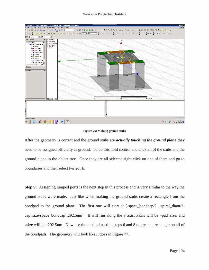
Worcester Polytechnic Institute
Page | 94
Figure 76: Making ground stubs
After the geometry is correct and the ground stubs are actually touching the ground plane they
need to be assigned officially as ground. To do this hold control and click all of the stubs and the
ground plane in the object tree. Once they are all selected right click on one of them and go to
boundaries and then select Perfect E.
Step 9: Assigning lumped ports is the next step in this process and is very similar to the way the
ground stubs were made. Just like when making the ground stubs create a rectangle from the
bondpad to the ground plane. The first one will start at [-space_bondcap/2 ,-spiral_diam/2-
cap_size-space_bondcap ,292.5um]. It will run along the y axis, xaxis will be –pad_size, and
zsize will be -292.5um. Now use the method used in steps 6 and 8 to create a rectangle on all of
the bondpads. The geometry will look like it does in Figure 77.

Worcester Polytechnic Institute
Page | 95
Figure 77: Creating and assigning lumped ports
After the geometry is all set the lumped ports will need to be assigned. To do this right-click on
the first plane connecting the bondpad to ground and navigate to assign excitation->lumped port.
Once clicked a menu will pop up asking for the full port impedance, leave the resistance at 50Ω
and reactance at 0Ω and click next. In this menu there should be one mode with no integration
line. Click on none under integration line and select new line. Now click at the top of the
rectangle, which is attached to the rest of the circuit, and then at the bottom of the rectangle,
which should be touching ground. Then click next, leave the option to renormalize all modes to
50Ω and click finish. When assigning the integration line the port should look like Figure 78.
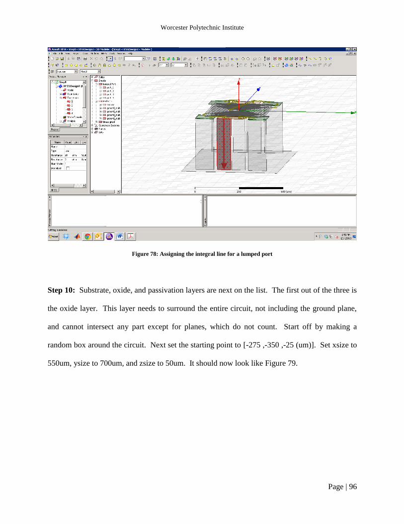
Worcester Polytechnic Institute
Page | 96
Figure 78: Assigning the integral line for a lumped port
Step 10: Substrate, oxide, and passivation layers are next on the list. The first out of the three is
the oxide layer. This layer needs to surround the entire circuit, not including the ground plane,
and cannot intersect any part except for planes, which do not count. Start off by making a
random box around the circuit. Next set the starting point to [-275 ,-350 ,-25 (um)]. Set xsize to
550um, ysize to 700um, and zsize to 50um. It should now look like Figure 79.
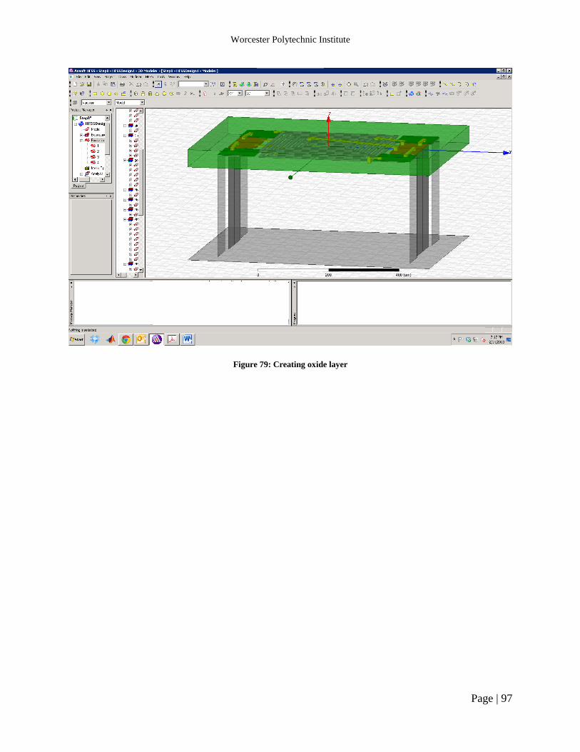
Worcester Polytechnic Institute
Page | 97
Figure 79: Creating oxide layer
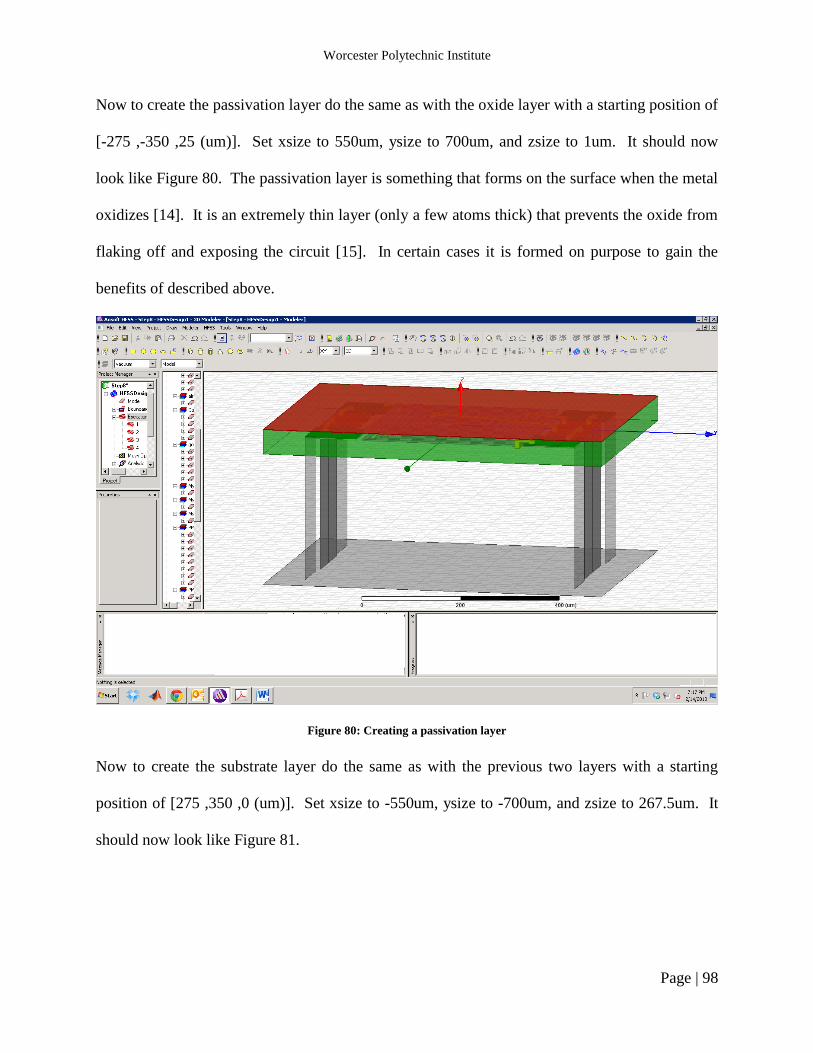
Worcester Polytechnic Institute
Page | 98
Now to create the passivation layer do the same as with the oxide layer with a starting position of
[-275 ,-350 ,25 (um)]. Set xsize to 550um, ysize to 700um, and zsize to 1um. It should now
look like Figure 80. The passivation layer is something that forms on the surface when the metal
oxidizes [14]. It is an extremely thin layer (only a few atoms thick) that prevents the oxide from
flaking off and exposing the circuit [15]. In certain cases it is formed on purpose to gain the
benefits of described above.
Figure 80: Creating a passivation layer
Now to create the substrate layer do the same as with the previous two layers with a starting
position of [275 ,350 ,0 (um)]. Set xsize to -550um, ysize to -700um, and zsize to 267.5um. It
should now look like Figure 81.
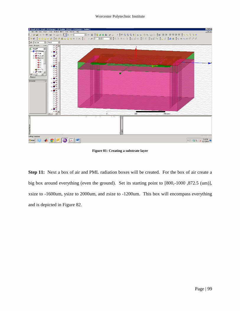
Worcester Polytechnic Institute
Page | 99
Figure 81: Creating a substrate layer
Step 11: Next a box of air and PML radiation boxes will be created. For the box of air create a
big box around everything (even the ground). Set its starting point to [800,-1000 ,872.5 (um)],
xsize to -1600um, ysize to 2000um, and zsize to -1200um. This box will encompass everything
and is depicted in Figure 82.
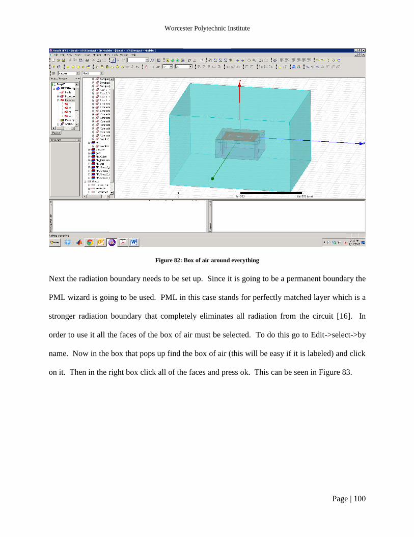
Worcester Polytechnic Institute
Page | 100
Figure 82: Box of air around everything
Next the radiation boundary needs to be set up. Since it is going to be a permanent boundary the
PML wizard is going to be used. PML in this case stands for perfectly matched layer which is a
stronger radiation boundary that completely eliminates all radiation from the circuit [16]. In
order to use it all the faces of the box of air must be selected. To do this go to Edit->select->by
name. Now in the box that pops up find the box of air (this will be easy if it is labeled) and click
on it. Then in the right box click all of the faces and press ok. This can be seen in Figure 83.

Worcester Polytechnic Institute
Page | 101
Figure 83: Selecting all face of the box of air
Now go to HFSS>Boundaries>PML Wizard. All of the default options will be used so just
keep pressing next. Now sit back and watch as boxes form around the box of air, as seen in
Figure 84. After they are created click on finish.

Worcester Polytechnic Institute
Page | 102
Figure 84: Using PML wizard
Step 12: Next is assigning the material. To do this we select all of the objects that possess the
same material. For this circuit first select the piece that was united early with both of the spiral
inductors, also select all four of the bottom capacitor plates. Right click one of the selected
objects and click on assign material. For these the material gold will be chosen; you can scroll
and find it in the list and select it byclicking ok once.
Next select the box of air that the radiation boxes are based off of. Follow the process
above to assign the material to air. Once this is complete follow the same process with all of the
cap via’s which uses a gallium arsenide material. For best effect this material will need to be
created. To do this navigate to the assign material menu where a button called create material
along the bottom row will be found. Click on this and another menu will pop up. In this change

Worcester Polytechnic Institute
Page | 103
the relative permittivity to 6.4 and leave the rest at their default values, do not forget to give it a
name, such as cap_via.
After this select the oxide layer and repeat the same process of creating a new material,
this one with relative permittivity at 6.4. For the passivation layer set a relative permittivity to
7.9. For the substrate set the material to silicon. The object tree should now have many
different materials listed in it with nothing labeled as vacuum.
Step 13: Next comes setting up the solution. To set up the solution you go to the very left of the
screen and into the project manager. If the box is not there simply go to view and select it. In
the manager scroll down to analysis and right click, selecting the add solution setup. In this box
set the solution frequency to 1.9GHz and under the adaptive passes section set max number of
passes to eight and max delta S to .001. Under the advanced tab make sure use radiation
boundary on ports is checked and that save fields is checked.
Now that the solution setup is set up right click on it and select add frequency sweep.
This will sweep the solution from the max value to the min allowing the ability to create nice
graphs. In the frequency sweep options select interpolating and linear step. Start at a frequency
of 1GHz and stop at 5GHz with a step size of 0.1GHz. When finish you press ok.
Step 14: Now the design should be ready to simulate. Before this can be done double check that
nothing is missing by clicking the validate check mark in the upper toolbars. Once it gives you
all check marks close the window and click the exclamation point to start the simulator and
generate some results. Warning: this can take from a few minutes to a few hours depending upon
the computers processing power.

Worcester Polytechnic Institute
Page | 104
When the simulator is complete go to the project manager and right click on results. The
most useful plots for this circuit are the S-parameter ones. To create these go to create modal
solution data report ->rectangular plot. Then select S(2,1) and S(3,1) making sure they are in dB,
and click on new report at the bottom of the window. Click close to view results. This process
can be repeated to give the difference in phase, which is the most important plot of this circuit.
To find the difference in phase type ang_deg(S(3,1)/S(2,1)) into the y component and select new
report. For different plots experiment with all of the options to get exactly what is required.
Another very useful result is plotting the electric field onto the circuit itself and seeing
the distribution. In order to do this go back to the 3D model by clicking on HFSSDesign in the
project manager and select all of the objects. Then go to HFSS->fields->plot fields->E->mag_E.
The electric field distribution should now be seen in the 3D modeler window.
All of these results and others can be found in HFSS Results.
Step 15: Other options in HFSS include the ability to set up optimizations. This is an extremely
helpful option as it automatically hones in on the answer that is needed by changing designated
variables. To designate these variables go to HFSSD>Design Properties click on the
optimization radio button and select the desired variables. Next right click on optimetrics in the
project manager window and select an optimization that is wanted, the normal one is add-
>optimization. The best optimizer is the quasi newton but this may vary depending upon the
circuit. Next setup calculation goals by clicking on setup calculations. The goals of this circuit
is to have -3dB (half power) at S(2,1) and S(3,1) and -90degrees at S(3,1)/S(2,1). Then go into
the variables tab and be sure to change the min and max values, along with the step size.
Beware, the more points used in the optimization the more time it will take, and since it is a
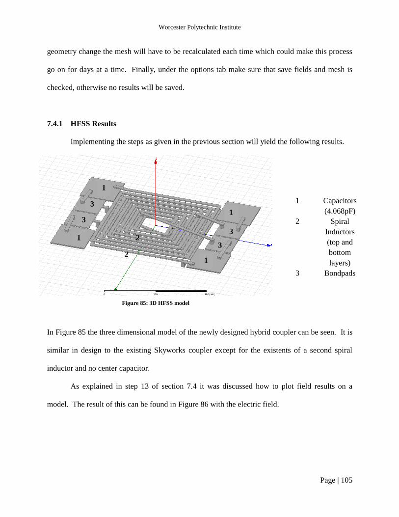
Worcester Polytechnic Institute
Page | 105
geometry change the mesh will have to be recalculated each time which could make this process
go on for days at a time. Finally, under the options tab make sure that save fields and mesh is
checked, otherwise no results will be saved.
7.4.1 HFSS Results
Implementing the steps as given in the previous section will yield the following results.
Figure 85: 3D HFSS model
1 Capacitors
(4.068pF)
2 Spiral
Inductors
(top and
bottom
layers)
3 Bondpads
In Figure 85 the three dimensional model of the newly designed hybrid coupler can be seen. It is
similar in design to the existing Skyworks coupler except for the existents of a second spiral
inductor and no center capacitor.
As explained in step 13 of section 7.4 it was discussed how to plot field results on a
model. The result of this can be found in Figure 86 with the electric field.
1
1
`
`
1
1
3
3
3
3
2
2
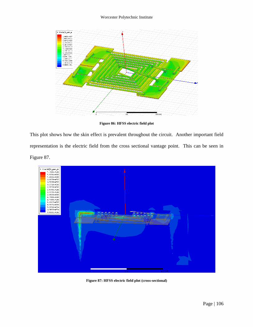
Worcester Polytechnic Institute
Page | 106
Figure 86: HFSS electric field plot
This plot shows how the skin effect is prevalent throughout the circuit. Another important field
representation is the electric field from the cross sectional vantage point. This can be seen in
Figure 87.
Figure 87: HFSS electric field plot (cross-sectional)

Worcester Polytechnic Institute
Page | 107
From this view point the build-up of the electric field around ports one and four is prevalent.
Next, for the results, are the most important S-parameters, in this case are S21 and S31. They can
be seen in Figure 88 along with some of the optimized results.
Figure 88: HFSS s-parameter magnitude
From this graph, around the frequency of 1.5GHz, the two parameters cross near -6.3dB.
Around the center frequency of 1.9GHz they have already started to diverge but are still within a
magnitude of -6.5dB. The goal was to get near 3dB attenuation but unfortunately this circuit did
not meet those expectations.
1.00 1.50 2.00 2.50 3.00 3.50 4.00 4.50 5.00
Freq [GHz]
-8.00
-7.80
-7.60
-7.40
-7.20
-7.00
-6.80
-6.60
-6.40
-6.20
Ma
gn
itud
e (
dB
)
HFSSDesign1Magnitude ANSOFT
Curve Info
dB(S(2,1))
Setup1 : Sw eep
spiral_diam='300um'
dB(S(2,1))
Setup1 : Sw eep
spiral_diam='300.8449168um'
dB(S(2,1))
Setup1 : Sw eep
spiral_diam='324.110939um'
dB(S(2,1))
Setup1 : Sw eep
spiral_diam='325um'
dB(S(2,1))
Setup1 : Sw eep
spiral_diam='325.0000211um'
dB(S(2,1))
Setup1 : Sw eep
spiral_diam='325.889061um'
dB(S(2,1))
Setup1 : Sw eep
spiral_diam='326.7781009um'
dB(S(2,1))
Setup1 : Sw eep
spiral_diam='338.6473653um'
dB(S(2,1))
Setup1 : Sw eep
spiral_diam='355um'
dB(S(3,1))
Setup1 : Sw eep
spiral_diam='300um'
dB(S(3,1))
Setup1 : Sw eep
spiral_diam='300.8449168um'
dB(S(3,1))
Setup1 : Sw eep
spiral_diam='324.110939um'
dB(S(3,1))
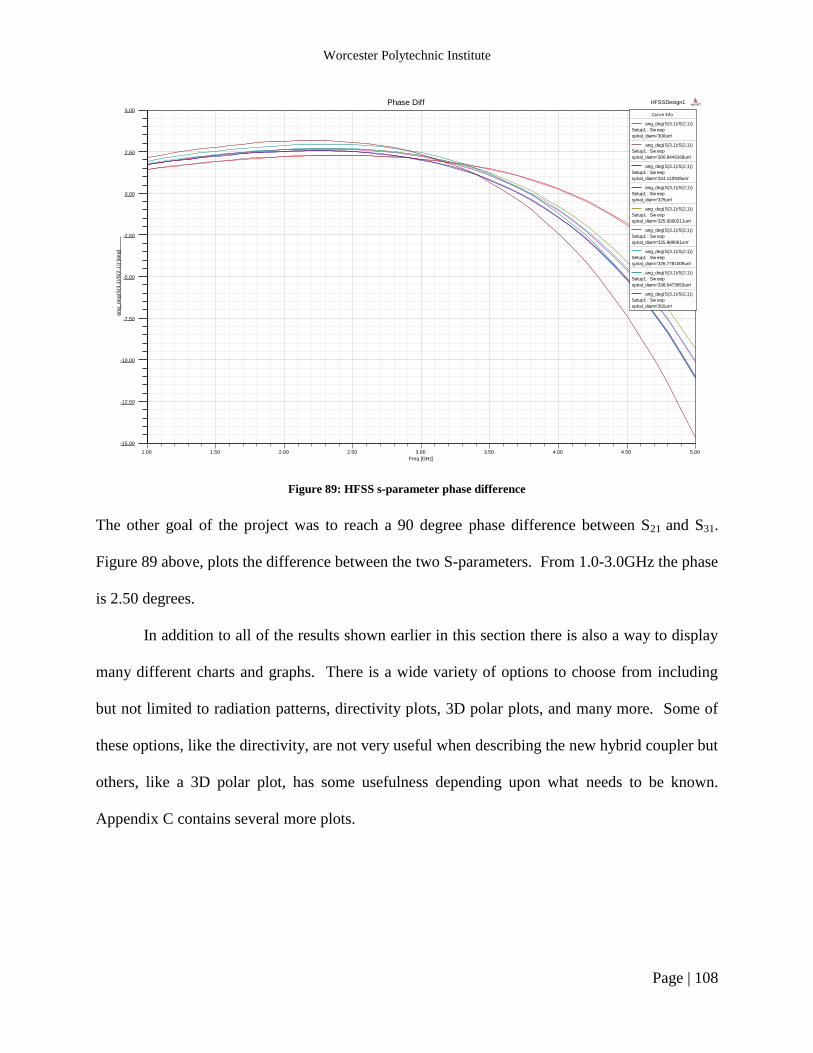
Worcester Polytechnic Institute
Page | 108
Figure 89: HFSS s-parameter phase difference
The other goal of the project was to reach a 90 degree phase difference between S21 and S31.
Figure 89 above, plots the difference between the two S-parameters. From 1.0-3.0GHz the phase
is 2.50 degrees.
In addition to all of the results shown earlier in this section there is also a way to display
many different charts and graphs. There is a wide variety of options to choose from including
but not limited to radiation patterns, directivity plots, 3D polar plots, and many more. Some of
these options, like the directivity, are not very useful when describing the new hybrid coupler but
others, like a 3D polar plot, has some usefulness depending upon what needs to be known.
Appendix C contains several more plots.
1.00 1.50 2.00 2.50 3.00 3.50 4.00 4.50 5.00
Freq [GHz]
-15.00
-12.50
-10.00
-7.50
-5.00
-2.50
0.00
2.50
5.00
an
g_
de
g(S
(3,1
)/S
(2,1
)) [d
eg
]
HFSSDesign1Phase Diff ANSOFT
Curve Info
ang_deg(S(3,1)/S(2,1))
Setup1 : Sw eep
spiral_diam='300um'
ang_deg(S(3,1)/S(2,1))
Setup1 : Sw eep
spiral_diam='300.8449168um'
ang_deg(S(3,1)/S(2,1))
Setup1 : Sw eep
spiral_diam='324.110939um'
ang_deg(S(3,1)/S(2,1))
Setup1 : Sw eep
spiral_diam='325um'
ang_deg(S(3,1)/S(2,1))
Setup1 : Sw eep
spiral_diam='325.0000211um'
ang_deg(S(3,1)/S(2,1))
Setup1 : Sw eep
spiral_diam='325.889061um'
ang_deg(S(3,1)/S(2,1))
Setup1 : Sw eep
spiral_diam='326.7781009um'
ang_deg(S(3,1)/S(2,1))
Setup1 : Sw eep
spiral_diam='338.6473653um'
ang_deg(S(3,1)/S(2,1))
Setup1 : Sw eep
spiral_diam='355um'

Worcester Polytechnic Institute
Page | 109
8 Results
Skyworks’ initial design for the coupler with a center frequency of 1.90GHz functioned
properly over the 1.85GHz-1.99GHz range yielding a bandwidth of 7.37%. The new design
yields an operational range between the frequencies 1.575GHZ-2.111GHz increasing the
bandwidth to 18.42%. Additionally, the layout for this new model resulted in having an area of
530x380um, compared to the old 860x640um. Table 2 shows a summary comparing the current
Skyworks design to the new one.
Table 2: Comparison of Skyworks model to WPI design
A significant drawback that can be observed is the fact that the new capacitor value is
significantly larger than the previously implemented capacitors. In implementation this design
would call for a larger area. Fortunately, the new design does not require a coupling capacitor to
be placed between the inductors, and therefore the design of the spiral inductor was adjusted to
make better use of the total area inside the spirals. By removing this capacitor the new design
achieves a more stable operation for the required ranges.

Worcester Polytechnic Institute
Page | 110
9 Conclusion
The main project goals were to increase the bandwidth of the 90-degree hybrid coupler
and to attempt to decrease the device area. These goals were successfully achieved as seen in the
previous sections with a bandwidth increase of 150%, while also reducing the device area by
63.46%.
Currently, Skyworks offers two separate devices: one at 1.85GHz-1.99GHz operation and
another device at 1.71GHz-1.88GHz. With the new developed design, the new design could
easily cover the entire spectrum required by these two devices. However, the implementation of
this device would require Skyworks to modify its fabrication process. This is because our design
has two extra metal layers on top of the existing fabrication process. Changing that process
would require a significant time and monetary investment. If Skyworks is willing to do this, they
might be able to satisfy the two different frequencies with a single chip.

Worcester Polytechnic Institute
Page | 111
10 Future Improvements
In ideal lumped components the redesign of the hybrid coupler in this report proved to
have excellent results. When those components were translated over to distributed elements,
unfortunately the results did not meet expectations. One future improvement that can be pursued
is to investigate the distributed circuit implementation side and study needed modifications.
Obviously, a distributed element solution represents a more viable solution as it eliminates the
parasitic behavior of lumped elements.
Moreover, in order to reduce the area of the circuit topology a few more layers were
added, making the whole circuit smaller but at the expense of a taller realization. An
improvement would be to take this design and reduce the height so that the number of overall
layers is reduced. This would allow the hybrid coupler to be manufactured within the limitations
of the Skyworks fabrication process.

Worcester Polytechnic Institute
Page | 112
Appendix A
Below is the MATLAB code used to import and interpret the results taken from the
network analyzer.
% James Corsini % importing data from network analyzer
clear all; close all; clc; % change the variable mynum to the case that you want to see mynum=5; switch mynum case 1 % Ecal 90 Degree Hybrid Device 1 directory = '\\ece-homes.ece.wpi.edu\jncorsini\MQP\WPI Data\WPI Data\ECal\90-DEGREE
HYBRID\Device 1'; filename = 'SMATRIX.s4p'; head='Ecal 90 Degree Hybrid Device 1'; case 2 % Ecal 90 Degree Hybrid Device 2 directory = '\\ece-homes.ece.wpi.edu\jncorsini\MQP\WPI Data\WPI Data\ECal\90-DEGREE
HYBRID\Device 2'; filename = 'SMATRIX.s4p'; head='Ecal 90 Degree Hybrid Device 2'; case 3 % Ecal 90 Degree Hybrid Device 3 directory = '\\ece-homes.ece.wpi.edu\jncorsini\MQP\WPI Data\WPI Data\ECal\90-DEGREE
HYBRID\Device 3'; filename = 'SMATRIX.s4p'; head='Ecal 90 Degree Hybrid Device 3'; case 4 % Ecal 90 Degree Hybrid Device 4 directory = '\\ece-homes.ece.wpi.edu\jncorsini\MQP\WPI Data\WPI Data\ECal\90-DEGREE
HYBRID\Device 4'; filename = 'SMATRIX.s4p'; head='Ecal 90 Degree Hybrid Device 4'; case 5 % Ecal Thru Device 1 directory = '\\ece-homes.ece.wpi.edu\jncorsini\MQP\WPI Data\WPI Data\ECal\THRU\Device 1'; filename = 'THRU.s2p'; head='Ecal Thru Device 1'; case 6 % Ecal Thru Device 2 directory = '\\ece-homes.ece.wpi.edu\jncorsini\MQP\WPI Data\WPI Data\ECal\THRU\Device 2'; filename = 'THRU.s2p'; head='Ecal Thru Device 2'; case 7 % Ecal Thru Device 3 directory = '\\ece-homes.ece.wpi.edu\jncorsini\MQP\WPI Data\WPI Data\ECal\THRU\Device 3'; filename = 'THRU.s2p'; head='Ecal Thru Device 3'; case 8 % Ecal Thru Device 4 directory = '\\ece-homes.ece.wpi.edu\jncorsini\MQP\WPI Data\WPI Data\ECal\THRU\Device 4'; filename = 'THRU.s2p'; head='Ecal Thru Device 4'; case 9 % TRL 90 Degree Hybrid Device 1 directory = '\\ece-homes.ece.wpi.edu\jncorsini\MQP\WPI Data\WPI Data\TRL\90-DEGREE
HYBRID\Device 1'; filename = 'SMATRIX.s4p'; head='TRL 90 Degree Hybrid Device 1'; case 10

Worcester Polytechnic Institute
Page | 113
% TRL 90 Degree Hybrid Device 2 directory = '\\ece-homes.ece.wpi.edu\jncorsini\MQP\WPI Data\WPI Data\TRL\90-DEGREE
HYBRID\Device 2'; filename = 'SMATRIX.s4p'; head='TRL 90 Degree Hybrid Device 2'; case 11 % TRL 90 Degree Hybrid Device 3 directory = '\\ece-homes.ece.wpi.edu\jncorsini\MQP\WPI Data\WPI Data\TRL\90-DEGREE
HYBRID\Device 3'; filename = 'SMATRIX.s4p'; head='TRL 90 Degree Hybrid Device 3'; case 12 % TRL 90 Degree Hybrid Device 4 directory = '\\ece-homes.ece.wpi.edu\jncorsini\MQP\WPI Data\WPI Data\TRL\90-DEGREE
HYBRID\Device 4'; filename = 'SMATRIX.s4p'; head='TRL 90 Degree Hybrid Device 4'; end
if (mynum==5||mynum==6||mynum==7||mynum==8) display('Only two ports') s_parameters = import_sNp(directory,filename);
S11_dB = squeeze(s_parameters.dB(1,1,:)); S12_dB = squeeze(s_parameters.dB(1,2,:)); S21_dB = squeeze(s_parameters.dB(2,1,:)); S22_dB = squeeze(s_parameters.dB(2,2,:)); freq = s_parameters.freq;
figure(1); plot(freq,S11_dB,'color',[0.75 0 0]); title([head,' S11/21 (dB)']); xlabel('Frequency (GHz)'); ylabel('S-Parameter Magnitude (dB)'); hold on; grid on; plot(freq,S12_dB,'color',[0 0 0.75]); plot(freq,S21_dB,'color',[0 0.75 0]); plot(freq,S22_dB,'color',[0.25 0 0]); else s_parameters = import_sNp(directory,filename);
phase_S21_unwrap = (180/pi)*unwrap((pi/180)*squeeze(s_parameters.phase(2,1,:))); phase_S31_unwrap = (180/pi)*unwrap((pi/180)*squeeze(s_parameters.phase(3,1,:))); S21_dB = squeeze(s_parameters.dB(2,1,:)); S31_dB = squeeze(s_parameters.dB(3,1,:)); amp_diff = S21_dB - S31_dB; phase_diff = phase_S21_unwrap - phase_S31_unwrap; freq = s_parameters.freq; f_low = 1.8; f_high = 2.0;
figure(1); plot(freq,S21_dB,'color',[0.75 0 0]); xlabel('Frequency (GHz)'); ylabel('S-Parameter Magnitude (dB)'); title([head,' S21/31 (dB)']); hold on; grid on; plot(freq,S31_dB,'color',[0 0 0.75]); figure(2); plot(freq,amp_diff,'color',[0 0.75 0]); xlabel('Frequency (GHz)'); ylabel('S-Parameter Magnitude (dB)'); grid on; title([head,' Amp Diff']); ylim([-2 0]); xlim([f_low f_high]); figure(3); plot(freq,phase_diff,'color',[0 0.75 0]);

Worcester Polytechnic Institute
Page | 114
xlabel('Frequency (GHz)'); ylabel('S-Parameter Phase (degrees)'); title([head,' Phase Diff']); grid on; ylim([-110 -70]); end
Following are the graphs for devices 2-4 for the electronic calibration.

Worcester Polytechnic Institute
Page | 115
Figure A.1: Hybrid Coupler 2 S21 and S31 Magnitude (dB)
Figure A.2: Hybrid Coupler 2 S21 and S31 Amplitude
Difference
Figure A.3: Hybrid Coupler 2 S21 and S31 Phase Difference
(degrees)
Figure A.4: Hybrid Coupler 3 S21 and S31 Magnitude (dB)
0 1 2 3 4 5 6 7 8-80
-70
-60
-50
-40
-30
-20
-10
0
Frequency (GHz)
S-P
aram
eter
Mag
nitu
de (d
B)
Ecal 90 Degree Hybrid Device 2 S21/31 (dB)
1.8 1.82 1.84 1.86 1.88 1.9 1.92 1.94 1.96 1.98 2-2
-1.8
-1.6
-1.4
-1.2
-1
-0.8
-0.6
-0.4
-0.2
0
Frequency (GHz)
S-P
aram
eter
Mag
nitu
de (d
B)
Ecal 90 Degree Hybrid Device 2 Amp Diff
0 1 2 3 4 5 6 7 8-110
-105
-100
-95
-90
-85
-80
-75
-70
Frequency (GHz)
S-P
aram
eter
Pha
se (d
egre
es)
Ecal 90 Degree Hybrid Device 2 Phase Diff
0 1 2 3 4 5 6 7 8-80
-70
-60
-50
-40
-30
-20
-10
0
Frequency (GHz)
S-P
aram
eter
Mag
nitu
de (d
B)
Ecal 90 Degree Hybrid Device 3 S21/31 (dB)

Worcester Polytechnic Institute
Page | 116
Figure A.5: Hybrid Coupler 3 S21 and S31 Amplitude
Difference
Figure A.6: Hybrid Coupler 3 S21 and S31 Phase Difference
(degrees)
Figure A.7: Hybrid Coupler 3 S21 and S31 Magnitude (dB)
Figure A.8: Hybrid Coupler 4 S21 and S31 Amplitude
Difference
Figure A.9: Hybrid Coupler 4 S21 and S31 Phase Difference (degrees)
1.8 1.82 1.84 1.86 1.88 1.9 1.92 1.94 1.96 1.98 2-2
-1.8
-1.6
-1.4
-1.2
-1
-0.8
-0.6
-0.4
-0.2
0
Frequency (GHz)
S-P
aram
eter
Mag
nitu
de (d
B)
Ecal 90 Degree Hybrid Device 3 Amp Diff
0 1 2 3 4 5 6 7 8-110
-105
-100
-95
-90
-85
-80
-75
-70
Frequency (GHz)
S-P
aram
eter
Pha
se (d
egre
es)
Ecal 90 Degree Hybrid Device 3 Phase Diff
0 1 2 3 4 5 6 7 8-80
-70
-60
-50
-40
-30
-20
-10
0
Frequency (GHz)
S-P
aram
eter
Mag
nitu
de (d
B)
Ecal 90 Degree Hybrid Device 4 S21/31 (dB)
1.8 1.82 1.84 1.86 1.88 1.9 1.92 1.94 1.96 1.98 2-2
-1.8
-1.6
-1.4
-1.2
-1
-0.8
-0.6
-0.4
-0.2
0
Frequency (GHz)
S-P
aram
eter
Mag
nitu
de (d
B)
Ecal 90 Degree Hybrid Device 4 Amp Diff
0 1 2 3 4 5 6 7 8-110
-105
-100
-95
-90
-85
-80
-75
-70
Frequency (GHz)
S-P
aram
eter
Pha
se (d
egre
es)
Ecal 90 Degree Hybrid Device 4 Phase Diff

Worcester Polytechnic Institute
Page | 117
Following are the graphs for devices 1-4 for the transmission line calibration.

Worcester Polytechnic Institute
Page | 118
Figure A.10: Hybrid Coupler 1 S21 and S31 Magnitude (dB)
Figure A.11: Hybrid Coupler 1 S21 and S31 Amplitude
Difference
Figure A.12: Hybrid Coupler 1 S21 and S31 Phase Difference
(degrees)
Figure A.13: Hybrid Coupler 2 S21 and S31 Magnitude
(dB)
Figure A.14: Hybrid Coupler 2 S21 and S31 Amplitude
Difference
Figure A.15: Hybrid Coupler 2 S21 and S31 Phase
Difference (degrees)
0 1 2 3 4 5 6 7 8-80
-70
-60
-50
-40
-30
-20
-10
0
Frequency (GHz)
S-P
aram
eter
Mag
nitu
de (d
B)
TRL 90 Degree Hybrid Device 1 S21/31 (dB)
1.8 1.82 1.84 1.86 1.88 1.9 1.92 1.94 1.96 1.98 2-2
-1.8
-1.6
-1.4
-1.2
-1
-0.8
-0.6
-0.4
-0.2
0
Frequency (GHz)
S-P
aram
eter
Mag
nitu
de (d
B)
TRL 90 Degree Hybrid Device 1 Amp Diff
0 1 2 3 4 5 6 7-110
-105
-100
-95
-90
-85
-80
-75
-70
Frequency (GHz)
S-P
aram
eter
Pha
se (d
egre
es)
TRL 90 Degree Hybrid Device 1 Phase Diff
0 1 2 3 4 5 6 7 8-80
-70
-60
-50
-40
-30
-20
-10
0
Frequency (GHz)
S-P
aram
eter
Mag
nitu
de (d
B)
TRL 90 Degree Hybrid Device 2 S21/31 (dB)
1.8 1.82 1.84 1.86 1.88 1.9 1.92 1.94 1.96 1.98 2-2
-1.8
-1.6
-1.4
-1.2
-1
-0.8
-0.6
-0.4
-0.2
0
Frequency (GHz)
S-P
aram
eter
Mag
nitu
de (d
B)
TRL 90 Degree Hybrid Device 2 Amp Diff
0 1 2 3 4 5 6 7 8-110
-105
-100
-95
-90
-85
-80
-75
-70
Frequency (GHz)
S-P
aram
eter
Pha
se (d
egre
es)
TRL 90 Degree Hybrid Device 2 Phase Diff

Worcester Polytechnic Institute
Page | 119
Figure A.16: Hybrid Coupler 3 S21 and S31 Magnitude (dB)
Figure A. 17: Hybrid Coupler 3 S21 and S31 Amplitude
Difference
Figure A. 18: Hybrid Coupler 3 S21 and S31 Phase Difference
(degrees)
Figure A. 19: Hybrid Coupler 4 S21 and S31 Magnitude
(dB)
Figure A. 20: Hybrid Coupler 4 S21 and S31 Amplitude
Difference
Figure A. 21: Hybrid Coupler 4 S21 and S31 Phase
Difference (degrees)
0 1 2 3 4 5 6 7 8-80
-70
-60
-50
-40
-30
-20
-10
0
Frequency (GHz)
S-P
aram
eter
Mag
nitu
de (d
B)
TRL 90 Degree Hybrid Device 3 S21/31 (dB)
1.8 1.82 1.84 1.86 1.88 1.9 1.92 1.94 1.96 1.98 2-2
-1.8
-1.6
-1.4
-1.2
-1
-0.8
-0.6
-0.4
-0.2
0
Frequency (GHz)
S-P
aram
eter
Mag
nitu
de (d
B)
TRL 90 Degree Hybrid Device 3 Amp Diff
0 1 2 3 4 5 6 7 8-110
-105
-100
-95
-90
-85
-80
-75
-70
Frequency (GHz)
S-P
aram
eter
Pha
se (d
egre
es)
TRL 90 Degree Hybrid Device 3 Phase Diff
0 1 2 3 4 5 6 7 8-80
-70
-60
-50
-40
-30
-20
-10
0
Frequency (GHz)
S-P
aram
eter
Mag
nitu
de (d
B)
TRL 90 Degree Hybrid Device 4 S21/31 (dB)
1.8 1.82 1.84 1.86 1.88 1.9 1.92 1.94 1.96 1.98 2-2
-1.8
-1.6
-1.4
-1.2
-1
-0.8
-0.6
-0.4
-0.2
0
Frequency (GHz)
S-P
aram
eter
Mag
nitu
de (d
B)
TRL 90 Degree Hybrid Device 4 Amp Diff
0 1 2 3 4 5 6 7 8-110
-105
-100
-95
-90
-85
-80
-75
-70
Frequency (GHz)
S-P
aram
eter
Pha
se (d
egre
es)
TRL 90 Degree Hybrid Device 4 Phase Diff

Worcester Polytechnic Institute
Page | 120
Appendix B
The voltage reflection coefficient is the ratio of the reflected and incident voltage wave at
the load. This ratio is shown in equation 1.
(B.1)
The voltage coefficient can be represented in terms of characteristic impedance and load
as shown in equation 2.
(B.2)
When the reflection coefficient is equal zero ( ), the load is matched to TL. Most
of the time is complex quantity therefore is complex quantity too. Also, depends on the
length of TL. It is described as shown in equation 3.
(B.3)
To find the input impedance at a particular point in TL, simply solve for from equation
two. The result is obtained in equation four.
( )
(B.4)
Now, substitute the reflection coefficient of equation three into equation four in order to
obtain the input impedance in terms of normalized impedance (
), characteristic
impedance, and phase constant (
). The equation five shows the result of this
mathematical manipulation.
( )
( ) (B.5)

Worcester Polytechnic Institute
Page | 121
If the length =
then . So, if half- lambda TL is added there is no loss on the
system. In case the length =
then
and if the system is matched and there
is zero reflection coefficient.

Worcester Polytechnic Institute
Page | 122
Appendix C
Figure C.1 Appendix: 3D polar plot
Figure C.2 Appendix: Directivity
-0.0005
-0.0004
-0.0002
-0.0001
90
60
30
0
-30
-60
-90
-120
-150
-180
150
120
HFSSDesign1Radiation Pattern 2 ANSOFT
Curve Info
DirTotal
Setup1 : LastAdaptive
Freq='1.9GHz' Phi='0deg' spiral_diam='300um'
DirTotal
Setup1 : LastAdaptive
Freq='1.9GHz' Phi='90deg' spiral_diam='300um'
DirTotal
Setup1 : LastAdaptive
Freq='1.9GHz' Phi='180deg' spiral_diam='300um'
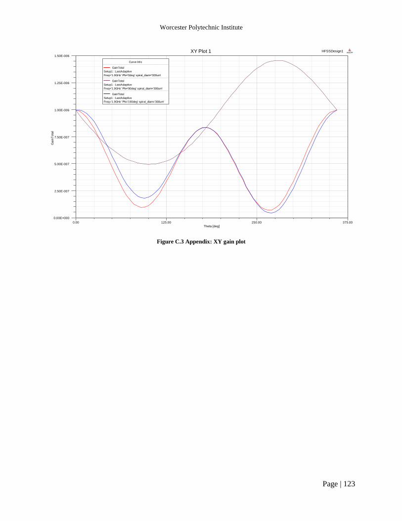
Worcester Polytechnic Institute
Page | 123
Figure C.3 Appendix: XY gain plot
0.00 125.00 250.00 375.00
Theta [deg]
0.00E+000
2.50E-007
5.00E-007
7.50E-007
1.00E-006
1.25E-006
1.50E-006
Ga
inT
ota
lHFSSDesign1XY Plot 1 ANSOFT
Curve Info
GainTotal
Setup1 : LastAdaptive
Freq='1.9GHz' Phi='0deg' spiral_diam='300um'
GainTotal
Setup1 : LastAdaptive
Freq='1.9GHz' Phi='90deg' spiral_diam='300um'
GainTotal
Setup1 : LastAdaptive
Freq='1.9GHz' Phi='190deg' spiral_diam='300um'

Worcester Polytechnic Institute
Page | 124
Appendix D
Figure D.4: Conversion between different network representations [7]

Worcester Polytechnic Institute
Page | 125
Figure D.5: ABCD-parameters of several two-port circuits [7]

Worcester Polytechnic Institute
Page | 126
Bibliography
[1] "Couplers and Splitters," 29 January 2010. [Online]. Available:
http://www.microwaves101.com/encyclopedia/couplers.cfm. [Accessed November 2012].
[2] "The Decibel Defined," 5 August 2008. [Online]. Available: http://sss-mag.com/db.html.
[Accessed September 2012].
[3] G. Breed, "Classic Design for Lumped Element and Transmission Line 90-Degree
Coupler," High Frequency Eletronics, pp. 62-66, September 2007.
[4] F. T. Ulaby, E. Michielssen and U. Ravaioli, Fundamentals of Applied Electromagnetics
(6th Edition), Prentice Hall, 2010.
[5] R. Ludwig and G. Bogdanov, RF Circuit Design: Theory & Applications (2nd Edition),
Prentice Hall, 2008.
[6] "Scattering Parameters," February 2013. [Online]. Available:
http://en.wikipedia.org/wiki/Scattering_parameters. [Accessed November 2012].
[7] Ansys HFSS, "Ansys HFSS," [Online]. Available:
http://www.ansys.com/Products/Simulation+Technology/Electromagnetics/High-
Performance+Electronic+Design/ANSYS+HFSS. [Accessed January 2013].
[8] MathWorks, "MATLAB," [Online]. Available:
http://www.mathworks.com/products/matlab/ . [Accessed January 2013].
[9] HyperPhysics, "Capacitance of Parallel Plates," 2000. [Online]. Available:
http://hyperphysics.phy-astr.gsu.edu/hbase/electric/pplate.html . [Accessed September
2012].
[10] S. S. Mohan, M. del Mar Hershenson, S. P. Boyd and T. H. Lee, "Simple Accurate
Expressions for Planar Spiral Inductances," IEEE Journal of Solid-State Circuits, pp. 1419-
1424, 1999.
[11] Skyworks Inc., "Markets," [Online]. Available: http://www.skyworksinc.com/Markets.aspx.
[Accessed February 2013].
[12] Skyworks Inc, "HY19-12,HY19-12LF: 90-Degree Hybrid 1.85-1.99GHz," 8 June 2006.
[Online]. Available: http://www.skyworksinc.com/uploads/documents/200234B.pdf.
[13] Stanford University, "Integrated Spiral Inductor Calculator," [Online]. Available:
http://www-smirc.stanford.edu/spiralCalc.html. [Accessed January 2013].
[14] J. Brubaker, "What Is Metal Oxide?," [Online]. Available:
http://www.ehow.com/about_6160418_metal-oxide-passivation_.html. [Accessed February

Worcester Polytechnic Institute
Page | 127
2013].
[15] NACE International, "The Passivation Layer," [Online]. Available:
http://events.nace.org/library/corrosion/Surface/Passivation-layer.asp. [Accessed February
2013].
[16] S. G. Johnson, "Notes on Perfectly Matched Layers (PMLs)," March 2010. [Online].
Available: http://math.mit.edu/~stevenj/18.369/pml.pdf. [Accessed February 2013].