6.776 Final Project 1.8GHz CMOS Transceiver Nathan...
12
6.776 Final Project – 1.8GHz CMOS Transceiver Nathan Monroe [email protected] 5/13/2016 Specifications Specified This Design Notes Center Frequency 1.8GHz 1.8GHz S11 -10dB min -10.95dB min 1.7-1.9GHz Voltage Gain 20dB 21.55dB RF to IF Noise Figure 6dB 3.7dB 100MHz Power 30mW 24.1mW Bonus: Phase Noise -120dBc/Hz -127.7dBc/Hz At df = 600KHz
Transcript of 6.776 Final Project 1.8GHz CMOS Transceiver Nathan...

6.776 Final Project – 1.8GHz CMOS Transceiver
Nathan Monroe
5/13/2016
Specifications
Specified This Design Notes
Center Frequency 1.8GHz 1.8GHz
S11 -10dB min -10.95dB min 1.7-1.9GHz
Voltage Gain 20dB 21.55dB RF to IF
Noise Figure 6dB 3.7dB 100MHz
Power 30mW 24.1mW
Bonus: Phase Noise -120dBc/Hz -127.7dBc/Hz At df = 600KHz


LNA Design Discussion
Power Gain Noise Figure S11 Kf Power
17.67dB 2.03dB -11.92dB 1.99 min 8.76mW
The LNA subcomponent was redesigned from the previously submitted design. The new Cascode-based
design has numerous advantages. First, it is a much smaller and more elegant design, yielding significant
area savings over previous 2-stge designs. In addition, the use of a single stage reduces power
significantly, while improving power gain and stability. The amplifier was designed using principles
discussed in class, using inductive degeneration for simultaneous noise and impedance matching for
optimal S11 and noise figure. The output was assumed to drive a 500 ohm plus 200fF load, representing
the mixer input. The LNA’s output inductor was designed to resonate with the load capacitance for
optimal S22 matching. The real mixer load was found to be slightly lower capacitance, so the LNA
inductor was tuned accordingly. See below for LNA schematic and test results.
LNA schematic

LNA Gain, Kf, Noise Figure
LNA Input/Output S parameters

LNA Power
Oscillator Design Discussion
Frequency Power Phase Noise (600KHz) Output Swing
1.7GHz 6.6mW -127.7dBc/Hz 3.2V (differential)
The Oscillator was also redesigned from previously submitted to improve performance. The redesign is
also based on the cross-coupled oscillator, based on design principles discussed in lecture and in
previous submissions. The redesign improves phase noise, power and output swing while sacrificing
tunability. The design was based on the assumption of a 150fF load, representing the gate capacitance
of the mixer. The mixer’s gate capacitance was found to be 56fF, therefore the system was tuned during
integration. See below for oscillator schematic and test results.

Oscillator Schematic
Oscillator output

Oscillator Phase Noise
Oscillator Power
Mixer Design Discussion
Voltage Gain Power Noise Figure
13.7dB 8.71mW (includes output buffer)
6.01dB
The mixer design was based on a single-balanced Gilbert cell mixer, consisting of a common source
transconductance stage driven by RF input, and a switching stage driven by the LO input. The mixer
stage itself consumes ~2mA. The mixer drives a differential NMOS source follower stage, which is used
to drive the 50 ohm (100 ohm differential) outputs. The large Gm required to drive the low load
impedance mandated large current in the output buffer stage of roughly 1.2mA per leg. A large Gm in
the mixing stage allows for large gain, some of which is sacrificed in the output buffer stage due to
heavy output loading. The choice of single balanced gilbert cell eliminates the need for a differentially-
driven RF port and allows for low power consumption and simplistic design, but has the downside of
large LO feedthrough to both RF and IF ports. Feedthrough to RF port results in self-mixing and a DC
component to the output. The mixer transistors are biased with current mirror transistors, sized for
minimum power draw.
Mixer schematic

Mixer Testbench
Mixer gain
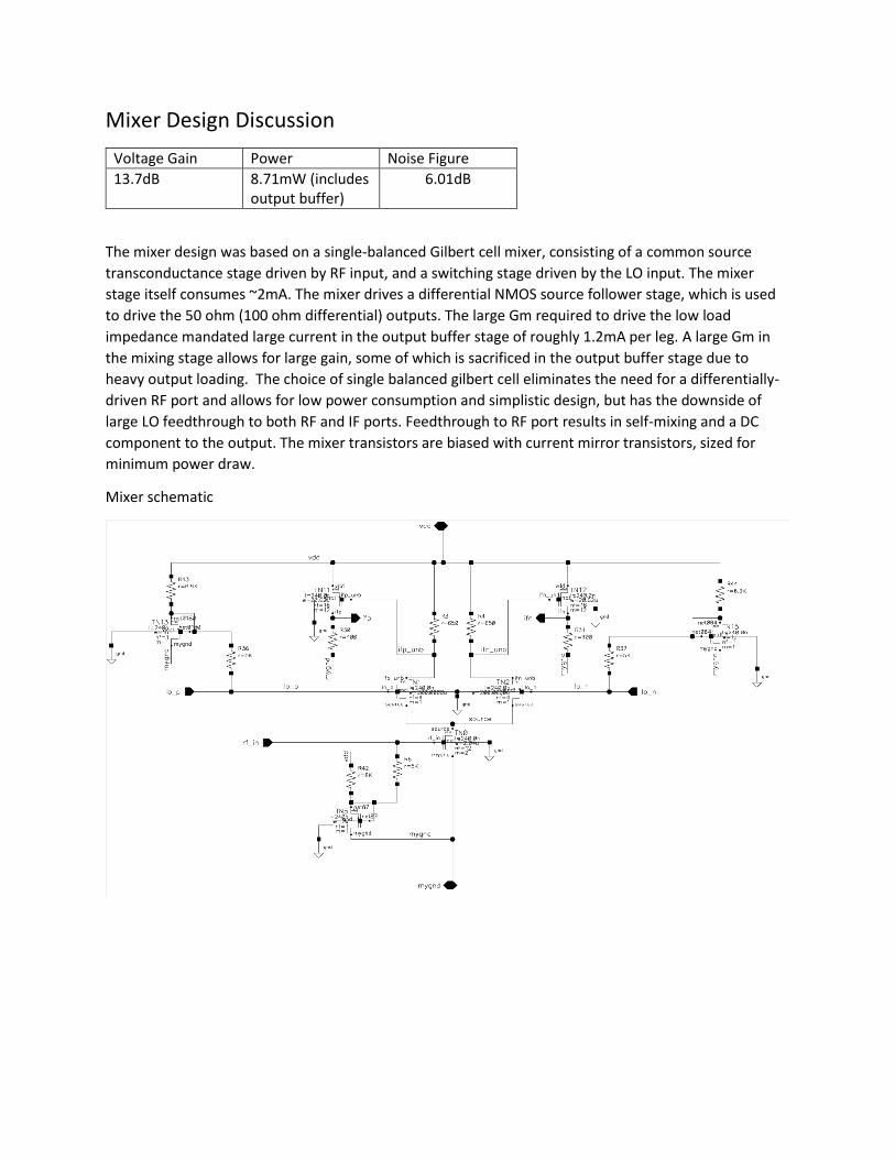
Mixer Noise Figure
Mixer Power Consumption (with output buffer)

System Integration Discussion
After designing all subcomponents with proper loading assumption, system integration was relatively
straightforward. The final value of gate capacitance load for the oscillator was found to be 56fF, so
additional loading of 94fF was added to correct oscillation frequency based on design assumption of
150fF load for proper oscillation frequency. In addition, output and input inductances of the LNA were
tuned to account for differences in loading than were predicted during design time. Ground bounce
caused by high dI/dt switching currents in the mixer through parasitic bondwire inductance was found
to cause an unexpected instability in the LNA, leading to PSS convergence issues in Cadence. This was
corrected by the addition of a separate grounding bondwire for the LNA. Due to the high gain of the
system, noise figure came well within specification despite high NF of the mixing stage. The cascode
architecture of the LNA yielded significant power savings, resulting in power consumption well below
specification. The output buffer stage could have perhaps been tuned for reduced power and gain
improvement, however both of these were within specification. Because the output buffer is driving a
differential load, no coupling capacitors were necessary, saving cost. At IF frequencies of 100MHz, such
capacitors would be large and costly.
System gain and S11
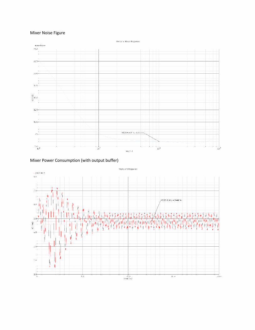
System noise figure
References
http://www.doe.carleton.ca/~jrogers/Bi.pdf
https://www.researchgate.net/publication/264396977_Design_and_Characterization_of_CMOS_Gilbert
_Mixer_at_130_nm_Technology_for_Impedance_Measurement_System_of_Human_Cell_in_Institute_f
or_Nanoelectronics#pf36
http://www.eecs.umich.edu/courses/eecs522/w11/project/group8report.pdf
https://filebox.ece.vt.edu/~symort/rfworkshop/Mixer_workshop_instruction.pdf
https://hal.inria.fr/hal-00947369/document
![Brochure2 - MagicBricks€¦ · Location Map School B sc Delhi Pub licSçh001 To 20 min 13 12 min 10 min 08 m] n 02 Temple AFMC 20 min 12 min IS min 10 min min IS min min 07 min](https://static.fdocuments.us/doc/165x107/6034384eb5808f20db6ba851/brochure2-magicbricks-location-map-school-b-sc-delhi-pub-licsh001-to-20-min.jpg)