40 W wide input range flyback converter demonstration ...€¦ · 40 W wide input range flyback...
34
June 2010 Doc ID 14630 Rev 2 1/34 AN2749 Application note 40 W wide input range flyback converter demonstration board for digital consumer equipment using the L6566B Introduction This document describes a demonstration board of a 40 W switch-mode power supply dedicated to set-top box, DVD and auxiliary SMPS for flat TVs or small size flat screen equipment. The board accepts a wide range of input voltages (90 to 265Vrms) and delivers 4 voltages. The design is based on the L6566B, a new current mode fixed frequency or QR controller. High efficiency and low standby consumption are the main characteristics of this board. These advantages, coupled with minimal part count required and low-cost approach of the global solution, make it a very interesting solution for powering digital consumer equipment, capable of meeting worldwide standby rules. Figure 1. EVL6566B-40WSTB demonstration board www.st.com
Transcript of 40 W wide input range flyback converter demonstration ...€¦ · 40 W wide input range flyback...

June 2010 Doc ID 14630 Rev 2 1/34
AN2749Application note
40 W wide input range flyback converter demonstration board for digital consumer equipment using the L6566B
IntroductionThis document describes a demonstration board of a 40 W switch-mode power supply dedicated to set-top box, DVD and auxiliary SMPS for flat TVs or small size flat screen equipment. The board accepts a wide range of input voltages (90 to 265Vrms) and delivers 4 voltages. The design is based on the L6566B, a new current mode fixed frequency or QR controller. High efficiency and low standby consumption are the main characteristics of this board. These advantages, coupled with minimal part count required and low-cost approach of the global solution, make it a very interesting solution for powering digital consumer equipment, capable of meeting worldwide standby rules.
Figure 1. EVL6566B-40WSTB demonstration board
www.st.com

Contents AN2749
2/34 Doc ID 14630 Rev 2
Contents
1 Main characteristics . . . . . . . . . . . . . . . . . . . . . . . . . . . . . . . . . . . . . . . . . 4
2 Circuit description . . . . . . . . . . . . . . . . . . . . . . . . . . . . . . . . . . . . . . . . . . . 6
3 Functional checking . . . . . . . . . . . . . . . . . . . . . . . . . . . . . . . . . . . . . . . . . 9
3.1 Full-load operation . . . . . . . . . . . . . . . . . . . . . . . . . . . . . . . . . . . . . . . . . . . 9
3.2 Reduced load operation, without the HDD . . . . . . . . . . . . . . . . . . . . . . . . 11
3.3 Minimum load operation . . . . . . . . . . . . . . . . . . . . . . . . . . . . . . . . . . . . . . 12
3.4 Wakeup time and startup . . . . . . . . . . . . . . . . . . . . . . . . . . . . . . . . . . . . . 16
3.5 Power down - hold-up time . . . . . . . . . . . . . . . . . . . . . . . . . . . . . . . . . . . . 18
3.6 Overload and overcurrent protection (OCP) . . . . . . . . . . . . . . . . . . . . . . . 19
3.7 Overvoltage protection (OVP) . . . . . . . . . . . . . . . . . . . . . . . . . . . . . . . . . 22
4 Conducted noise measurements . . . . . . . . . . . . . . . . . . . . . . . . . . . . . . 23
5 Thermal measures . . . . . . . . . . . . . . . . . . . . . . . . . . . . . . . . . . . . . . . . . . 24
6 Bill of material . . . . . . . . . . . . . . . . . . . . . . . . . . . . . . . . . . . . . . . . . . . . . 25
7 PCB layout . . . . . . . . . . . . . . . . . . . . . . . . . . . . . . . . . . . . . . . . . . . . . . . . 29
8 Transformer specifications . . . . . . . . . . . . . . . . . . . . . . . . . . . . . . . . . . 30
9 Conclusion . . . . . . . . . . . . . . . . . . . . . . . . . . . . . . . . . . . . . . . . . . . . . . . . 32
9.1 References . . . . . . . . . . . . . . . . . . . . . . . . . . . . . . . . . . . . . . . . . . . . . . . . 32
10 Revision history . . . . . . . . . . . . . . . . . . . . . . . . . . . . . . . . . . . . . . . . . . . 33
AN2749 List of figures
Doc ID 14630 Rev 2 3/34
List of figures
Figure 1. EVL6566B-40WSTB demonstration board . . . . . . . . . . . . . . . . . . . . . . . . . . . . . . . . . . . . . . 1Figure 2. Electrical diagram . . . . . . . . . . . . . . . . . . . . . . . . . . . . . . . . . . . . . . . . . . . . . . . . . . . . . . . . . 5Figure 3. EVL6566B-40WSTB waveforms at 115 Vac-60 Hz - full load . . . . . . . . . . . . . . . . . . . . . . . 9Figure 4. EVL6566B-40WSTB waveforms at 230 Vac-50 Hz - full load . . . . . . . . . . . . . . . . . . . . . . . 9Figure 5. EVL6566B-40WSTB waveforms at 265 V-50 Hz - full load . . . . . . . . . . . . . . . . . . . . . . . . 10Figure 6. EVL6566B-40WSTB waveforms at 230 V - Pin=30 W . . . . . . . . . . . . . . . . . . . . . . . . . . . . 13Figure 7. EVL6566B-40WSTB waveforms at 230 V - Pin=4 W . . . . . . . . . . . . . . . . . . . . . . . . . . . . 13Figure 8. EVL6566B-40WSTB waveforms at 265 Vac - no load . . . . . . . . . . . . . . . . . . . . . . . . . . . . 14Figure 9. EVL6566B-40WSTB waveforms at 265 Vac - no load (detail) . . . . . . . . . . . . . . . . . . . . . . 14Figure 10. Input power vs. mains voltage during standby . . . . . . . . . . . . . . . . . . . . . . . . . . . . . . . . . . 15Figure 11. Pin at 230 Vac vs. Iout 5 V . . . . . . . . . . . . . . . . . . . . . . . . . . . . . . . . . . . . . . . . . . . . . . . . . 15Figure 12. EVL6566B-40WSTB wakeup time at 115 Vac . . . . . . . . . . . . . . . . . . . . . . . . . . . . . . . . . . 16Figure 13. EVL6566B-40WSTB wakeup time at 230 Vac . . . . . . . . . . . . . . . . . . . . . . . . . . . . . . . . . . 16Figure 14. EVL6566B-40WSTB startup at 90 Vac - full load . . . . . . . . . . . . . . . . . . . . . . . . . . . . . . . . 17Figure 15. EVL6566B-40WSTB startup at 265 Vac - full load . . . . . . . . . . . . . . . . . . . . . . . . . . . . . . . 17Figure 16. EVL6566B-40WSTB hold-up time at 115 Vac - full load . . . . . . . . . . . . . . . . . . . . . . . . . . 18Figure 17. EVL6566B-40WSTB hold-up time at 230 Vac - full load . . . . . . . . . . . . . . . . . . . . . . . . . . 18Figure 18. EVL6566B-40WSTB output short +12 V at 90 V- full load . . . . . . . . . . . . . . . . . . . . . . . . . 19Figure 19. EVL6566B-40WSTB output short +12 V at 265 V- full load . . . . . . . . . . . . . . . . . . . . . . . . 19Figure 20. EVL6566B-40WSTB output short +1.8 V at 90 V- full load. . . . . . . . . . . . . . . . . . . . . . . . . 19Figure 21. EVL6566B-40WSTB output short +1.8 V at 265 V- full load. . . . . . . . . . . . . . . . . . . . . . . . 19Figure 22. EVL6566B-40WSTB output short +5 V at 90 V - full load . . . . . . . . . . . . . . . . . . . . . . . . . 20Figure 23. EVL6566B-40WSTB output short +5 V at 265 V - full load. . . . . . . . . . . . . . . . . . . . . . . . 20Figure 24. EVL6566B-40WSTB output short +3.3 V at 90 V - full load . . . . . . . . . . . . . . . . . . . . . . . . 20Figure 25. EVL6566B-40WSTB output short +3.3 V at 265 V - full load . . . . . . . . . . . . . . . . . . . . . . . 20Figure 26. EVL6566B-40WSTB output short +12 V at 90 V- no load . . . . . . . . . . . . . . . . . . . . . . . . . 21Figure 27. EVL6566B-40WSTB output short +12 V at 265 V- no load . . . . . . . . . . . . . . . . . . . . . . . . 21Figure 28. EVL6566B-40WSTB output short +1.8 V at 90 V- no load . . . . . . . . . . . . . . . . . . . . . . . . . 21Figure 29. EVL6566B-40WSTB output short +1.8 V at 265 V- no load . . . . . . . . . . . . . . . . . . . . . . . . 21Figure 30. EVL6566B-40WSTB OVP at 230 Vac- full load . . . . . . . . . . . . . . . . . . . . . . . . . . . . . . . . . 22Figure 31. EVL6566B-40WSTB OVP at 230 Vac- no load . . . . . . . . . . . . . . . . . . . . . . . . . . . . . . . . . 22Figure 32. EVL6566B-40WSTB conducted noise measurement phase A without frequency jittering . 23Figure 33. EVL6566B-40WSTB conducted noise measurement phase A with frequency jittering . . . 23Figure 34. EVL6566B-40WSTB thermal map at 115 Vac - full load . . . . . . . . . . . . . . . . . . . . . . . . . . 24Figure 35. EVL6566B-40WSTB thermal map at 230 Vac - full load . . . . . . . . . . . . . . . . . . . . . . . . . . 24Figure 36. Silk screen - top side . . . . . . . . . . . . . . . . . . . . . . . . . . . . . . . . . . . . . . . . . . . . . . . . . . . . . 29Figure 37. Silk screen - bottom side . . . . . . . . . . . . . . . . . . . . . . . . . . . . . . . . . . . . . . . . . . . . . . . . . . 29Figure 38. Transformer electrical diagram . . . . . . . . . . . . . . . . . . . . . . . . . . . . . . . . . . . . . . . . . . . . . . 30Figure 39. Transformer winding diagram . . . . . . . . . . . . . . . . . . . . . . . . . . . . . . . . . . . . . . . . . . . . . . . 31

Main characteristics AN2749
4/34 Doc ID 14630 Rev 2
1 Main characteristics
The main characteristics of this SMPS are listed below:
● Input voltage: Vin: 90 - 264 Vrms f: 45-66 Hz
● Output voltages as given in Table 1
● Standby: better than 800 mW at 230 Vin
● Short-circuit protection: on all outputs, with auto-restart at short removal
● PCB type and size: single-side 70 µm (2-Oz), CEM-1, 150 x 75 mm
● Safety: accordance with EN60065, creepage and clearance minimum distance 6.4 mm
● EMI: accordance with EN50022-Class B
Table 1. Output voltages
Vout IoutMAX IoutMIN PMAX Stability Notes
1.8 V 1.73 A 0.20 A 3.1 W ±7%Dedicated to digital circuitry and
to 1.2 V local post regulators
3.3 V 0.5 A 0.03 A 1.65 W ±5%Dedicated to analog peripherals
and 2.5 V regulators
5 V 2.4 A 0.3 A 12 W ±10%Dedicated to HDD/DVD and 5 V
circuitry
12 V1.9 Avg
2.9 Apk0.05 A 34.8 W ±8%
Dedicated to HDD/DVD, SCART and LNBP21 for satellite STB.
Average load is 1.9 A, 2.9 A is dedicated to HDD/DVD spin-up
POUT (W) = 40 W Avg / 51 W pk

AN2749 Main characteristics
Doc ID 14630 Rev 2 5/34
Figure 2. Electrical diagram

Circuit description AN2749
6/34 Doc ID 14630 Rev 2
2 Circuit description
The topology of this converter is the classical flyback, working in continuous and discontinuous conduction mode with fixed frequency, capable of achieving the best trade-off between the peak-to-rms current ratio and output capacitor size. The nominal switching frequency, 62 kHz, has been chosen to arrive at a compromise between the transformer size and the harmonics of the switching frequency, optimizing the input filter size and its cost. The input EMI filter is a classical Pi-filter, 1-cell for differential mode noise. An NTC (R1) limits the inrush current produced by the capacitor charging at plug-in. The MOSFET is a standard and inexpensive 600 V-2 Ω max, TO-220FP, needing just a small heat sink. The transformer is a layer type, using a standard ferrite type EER28L. It has been designed according to the EN60065 and it is manufactured by TDK. The reflected voltage is 70 V, providing enough room for the leakage inductance voltage spike with still margin for reliability of the MOSFET. The network D7, R7, C21 clamps the peak of the leakage inductance voltage spike.
The output rectifiers have been selected according to the maximum reverse voltage, forward-voltage drop and power dissipation. The rectifiers for 5 V and 12 V outputs are Schottky, low forward voltage drop type, hence dissipating less power with respect to standard types. They are housed in TO-220 package. A small heat sink for both devices is required, as indicated in the bill of material (BOM). The other two output rectifiers are Schottky too but with a smaller package. The snubber R2 and C7 damps the oscillation produced by the diode D2 at MOSFET turn-on. A small LC filter has been added on all outputs in order to filter the high frequency ripple without increasing the output capacitors and a capacitor (100 nF) has been placed on each output, to limit the spike amplitude.
The output voltage regulation is performed by secondary feedback sensing the 12 V, 5 V and 3.3 V outputs, while for 1.8 V output the regulation is achieved by the transformer coupling. The feedback network uses a TS2431 as error amplifier which drives an optocoupler SFH617A-4, insuring the required insulation between primary and secondary. The opto-transistor modulates directly the voltage on COMP pin of the L6566B.
The controller, the new L6566B, is an extremely versatile current mode primary controller embedding all functions needed to get very high performance power supplies. It also integrates all protections needed by a power supply offering a very high degree of flexibility to the designer.
Furthermore the L6566B has a soft-start (pin#14), disable (pin#8) and 5 V reference voltage VREF (pin#10) available.
Startup sequence
The L6566B pin #1 (HV) is directly connected to the DC bulk voltage and at startup, an internal high voltage current source charges C19 and C100 until the L6566B turn-on voltage threshold is reached, then the high voltage current source is automatically switched off. As the L6566B starts switching it is initially supplied by the VCC capacitor, and then the transformer auxiliary winding provides the voltage to power the IC. Because the L6566B integrated HV startup circuit is turned off, it is not dissipative during normal operation and has a significant role to reduce the power consumption when the power supply operates at light load. This contributes significantly to meet worldwide standby standards currently required.

AN2749 Circuit description
Doc ID 14630 Rev 2 7/34
Brownout protection
Brownout protection prevents the circuit from working with abnormal mains levels. It can be easily achieved using pin #16 (AC_OK) of the L6566B. The divider R5, R6, R46, R12 and R13 is connected to the input DC bus and it is dedicated to sense the rectified input voltage peak value and feed it into the L6566B AC_OK pin. An internal comparator then enables the IC operations if the mains level is correct, within the nominal limits. If the input voltage is below 85Vac, the startup of the circuit is inhibited, while the turnoff voltage has been set at the voltage reached by the bulk capacitor after the hold-up time. The internal comparator has in fact a current hysteresis allowing to set independently the L6566B turn-on and turnoff voltage.
L6566B current mode control and voltage feed-forward function
R18 and R19 sense the MOSFET current and the signal is fed into pin #7 (CS), connected to the PWM comparator. This signal is thus compared with the COMP (pin #9) signal, which is coming from the optocoupler.
The maximum power that the converter can deliver is set by a comparator limiting the peak of the primary current, comparing the CS and an internal threshold (VCSX). If the current signal exceeds the threshold, the comparator limits the MOSFET duty cycle, hence the output power is also limited.
Because the maximum transferable power depends on both the primary peak current and the input voltage, in order to keep almost constant the overload set point that would change according to flyback input voltage, the L6566B implements a voltage feed-forward function via a dedicated pin. Hence, VCSX is modulated by the voltage on pin #15 (VFF) sensing the bulk voltage by a resistor divider. A higher voltage causes a smaller VCS, MAX so that the maximum power can be kept almost constant at any input voltage.
The resistor R27 connected between pin #7 (CS) and pin #12 (MODE/SC) provides the correct slope compensation to the current signal, required for the correct loop stability.
L6566B short-circuit protection
In case of short-circuit, an internal comparator senses the COMP pin after the soft-start time. In that condition the COMP pin goes high, activating an internal current source that restarts charging the soft-start capacitor from the initial 2 V level. If the voltage on this pin reaches 5 V, the L6566B stops the operation and enters in "hiccup mode". The L6566B restarts with a startup sequence when the Vcc voltage drops below the Vcc restart level (5 V). Because of the long time needed by the Vcc capacitor to drop to 5 V, this results in an increase of the duration of the no-load operation, thus decreasing the power dissipation and the stress of the power components. This sequence is repeated until the short is removed, after that the normal operation of the converter is automatically resumed.
Another comparator having its threshold at 1.5 V dedicated to protecting the circuit in case of transformer saturation or secondary diodes short is provided too. If the voltage on the CS pin (#7) exceeds this threshold two consecutive times, the IC immediately shuts down and latches off. This is intended to prevent spurious activation of the protection in case of temporary disturbances, for example during the immunity tests. Even in this case the IC operation is resumed as soon as the Vcc voltage drops below 5 V. In this way a hiccup mode operation is still obtained, avoiding consequent failures due to overheating of the power components . The sequence described here effectively protects the circuit if during the short operation the power supply delivers a significant high power at the output. Sometimes, in multi-output SMPS in case of short on a low voltage output and especially when the power supply is not delivering the full load, the power delivered to the shorted output could be

Circuit description AN2749
8/34 Doc ID 14630 Rev 2
lower than the total maximum deliverable output power of the power supply. In that case the situation would be critical because the power supply is delivering a high output current that could overheat the secondary side components, but the reduced power at primary side would not be able to trigger the overload protection at primary side. Therefore, an output voltage sensing on the lower voltage is implemented. Thus, in case a low voltage output is shorted, the abnormal lower value of that output is detected and the COMP pin is tied to GND by Q2 and Q3, pushing the circuit to work in hiccup mode.
Overvoltage protection
The pin #11 (ZCD) is connected to the auxiliary winding by a resistor divider. It implements the OVP against feedback network failures. When the ZCD pin voltage exceeds 5 V, the IC is shut down. This protection can be set as latch or auto-restart by the user with no additional components. On the board it is set as latched. Therefore the operations can be resumed after a mains recycling.
Standby power saving and light-load frequency foldback function
The L6566B implements a current mode control, thus it monitors the output power by pin COMP, which level is proportional to the load. Thus, when the voltage on pin COMP falls below an internal threshold, the controller is disabled and its consumption reduced; Normal operation restarts as soon as the COMP voltage rises again. In this way a low consumption burst mode operation is obtained.
The burst mode feature is dedicated to reduce the no load consumption but another target of this application is achieving a high converter efficiency even at light load, when normally it is quite low. To improve the efficiency at this load condition a reduction of the switching frequency is needed, in order to save AC and transition losses of the power section. A simple circuit realizing a frequency foldback, connected to the L6566B oscillator (pin #13 -OSC) is implemented on the board. This solution allows improving light-load efficiency requiring just three external components.
Frequency jittering
To improve the EMI behavior of the application and make it quieter thus minimizing the EMI filter, the L6566B is provided with a dedicated pin, FMOD (#6), allowing the user the possibility to modulate the oscillator frequency in case the device is set for working in fixed frequency mode. The FMOD pin (#6) gives the possibility to select both the modulation frequency and the modulation depth. On the board, the capacitor C36 connected from this pin to GND is alternately charged and discharged by internal current sources. As a result, the voltage on the pin is a symmetrical triangular waveform with the frequency related to its value. By connecting a resistor (R31) from this pin to pin OSC (#13) it is possible to modulate the current sourced by the OSC pin and then the switching frequency. In this board a 400 Hz modulating frequency and ±5 kHz of frequency deviation have been set. The modulation reduces the peak value of EMI emissions by means of a spread-spectrum action. Please refer to Chapter 4: Conducted noise measurements on page 23 for the relevant measurements and comparison of the circuit working with or without the frequency jittering function.

AN2749 Functional checking
Doc ID 14630 Rev 2 9/34
3 Functional checking
3.1 Full-load operationThe following waveforms during normal operation at full load at different input voltages are shown for user reference:
Figure 3 shows the drain voltage and current waveforms at 115 Vac while in Figure 4 the waveforms are taken at 230 Vac. From the drain waveform it is possible to note that the transformer is working in continuous mode. This operating mode has been chosen in order to optimize the output filter capacitors and the peak-to-rms ratio of the current flowing in the transformer windings. The measured switching frequency is 61 kHz. In Figure 5, the drain voltage peak at full load and maximum input mains voltage has been measured. The maximum voltage peak in this condition is 530 V, ensuring a reliable operation of the MOSFET with good margin against its maximum BVDSS.
Figure 3. EVL6566B-40WSTB waveforms at 115 Vac-60 Hz - full load
Figure 4. EVL6566B-40WSTB waveforms at 230 Vac-50 Hz - full load
CH1: drain voltageCH2: L6566B pin#7 (CS)
CH1: drain voltageCH2: L6566B pin#7 (CS)

Functional checking AN2749
10/34 Doc ID 14630 Rev 2
Figure 5. EVL6566B-40WSTB waveforms at 265 V-50 Hz - full load
The following table shows the output voltage measurements and the overall efficiency of the converter measured at nominal input mains voltages. All output voltages have been measured on the output connector of the board.
In Table 2 it is possible to note that all voltages are within the tolerance given in the specification. The efficiency measured is very good for this kind of SMPS, thanks to the absence of post regulators.
In the followingTable 3 the output voltages are measured during the spin-up of the HDD or the DVD, meaning a temporary increasing of the 12 V output current supplying the motor. The other output voltage loads are unchanged.
Table 2. EVL6566B-STB-40W efficiency measurement at full load
Vin = 115 Vac-60 Hz Vin = 230 Vac-50 Hz
Voltage [V] Current [A] Deviation Voltage [V] Current [A] Deviation
11.94 1.9 -0.50% 11.82 1.9 -1.50%
1.77 1.7 -1.67% 1.79 1.7 -0.56%
4.89 2.4 -2.20% 4.89 2.4 -2.20%
3.33 0.5 0.91% 3.33 0.5 0.91%
Pout [W] = 39.10 Pout [W] = 38.9
Pin [W] = 50.6 Pin [W] = 48.95
Efficiency =77.26 % Efficiency =79.47 %
CH1: VdrainCH2: L6566B Isen

AN2749 Functional checking
Doc ID 14630 Rev 2 11/34
As observable in this table, the output voltages are still within the given tolerance. The heavier load does not affect efficiency. Please note that the total output power of Table 3 is the so-called "electrical power", not the "thermal power". Therefore, the circuit has been designed to deliver the "electrical power" for a short time only - typically the HDD spin-up has duration of 1 second - but it cannot be delivered significantly longer because, from the thermal point of view, the circuit can manage with the required reliability the full load only.
3.2 Reduced load operation, without the HDDThis reference board has been designed for powering digital equipment including a hard disk drive or a DVD but it can be used even for powering a set-top box or any other digital equipment without the hard disk drive. A typical example could be an auxiliary SMPS of a large screen flat-TV. The measurements shown in Table 4 provide for the output voltage and efficiency measurements in a load condition typical of a satellite set-top box.
The 12 V and 5 V output currents have been reduced with respect to the previous measurements. As visible the output voltages are within the tolerances and the efficiency is at the same level of the previous test results.
Table 3. EVL6566B-STB-40W efficiency measurement at HDD spin-up
Vin = 115 Vac-60 Hz Vin = 230 Vac-50 Hz
Voltage [V] Current [A] Deviation Voltage [V] Current [A] Deviation
11.75 2.9 -2.08% 11.66 2.9 -2.83%
1.77 1.7 -1.67% 1.79 1.7 -0.56%
4.83 2.4 -3.40% 4.85 2.4 -3.00%
3.35 0.5 1.52% 3.35 0.5 1.52%
Pout [W] = 50.35 Pout [W] = 50.17
Pin [W] = 66.4 Pin [W] = 62.94
Efficiency = 75.83 % Efficiency = 79.71 %
Table 4. Output voltage measurement at reduced load, without HDD
Vin = 115 Vac-60 Hz Vin = 230 Vac-50 Hz
Voltage Current Deviation Voltage Current Deviation
12.08 1.1 0.67% 12.09 1.1 0.75%
1.76 1.7 -2.22% 1.78 1.7 -1.11%
4.99 1.8 -0.20% 4.99 1.8 -0.20%
3.30 0.5 0.00% 3.3 0.5 0.00%
Pout [W] = 26.91 Pout [W] = 26.96
Pin [W] = 34.5 Pin [W] = 33.9
Efficiency = 78.01% Efficiency = 79.52%
Functional checking AN2749
12/34 Doc ID 14630 Rev 2
3.3 Minimum load operationEven at minimum load the power supply is still capable of regulating the output voltages within the specification tolerances, as indicated by the measurements in Table 5. The efficiency is still high.
Future new regulations and voluntary agreements for consumer and information technology equipment require that power supplies and adapters have high efficiency not only at nominal or maximum load but also at minimum and light load. In these conditions most of the time good efficiency is a difficult task to achieve, as it increases the complexity of control. By just adding a few external components, the oscillator structure of the L6566B can very easily implement a frequency foldback. Thus, the frequency reduction minimizes the switching losses, improving the power supply efficiency when it is working with an input power in the range of 1 to 30 W.
The L6566B switching frequency is set by the current flowing in a resistor connected between the OSC pin and ground (R15). During light-load operation the COMP (pin#9) level decreases and Q4 injects into R15 and OSC (pin #13) a current inversely proportional to the COMP voltage. Because the voltage on pin OSC is constant (1 V), increasing Q4 current provides for the decrease of the current supplied by the pin and, as a consequence, the oscillator frequency. Thus, a frequency reduction proportional to the output load is easily obtained.
Figure 6 and 7 show the waveforms at different input power consumption. It can be noted that the switching frequency is lower than the value measured at full load and decreases proportionally to the COMP pin level.
Table 5. Output voltage measurement at reduced load, without HDD
Vin = 115 Vac-60 Hz Vin = 230 Vac-50 Hz
Voltage [V] Current [A] Deviation Voltage [V] Current [A] Deviation
11.97 0.05 -0.25% 11.99 0.05 -0.08%
1.78 0.2 -1.11% 1.79 0.2 -0.56%
4.89 0.3 -2.20% 4.89 0.3 -2.20%
3.40 0.03 3.03% 3.40 0.03 3.03%
Pout [W] = 2.52 Pout [W] = 2.53
Pin [W] = 3.43 Pin [W] = 3.69
Efficiency = 73.57 % Efficiency = 68.47%

AN2749 Functional checking
Doc ID 14630 Rev 2 13/34
If the load is further decreased, the L6566B works in burst mode. Once the COMP (pin#9) voltage drops below the internal threshold, the L6566B stops the gate driver operation decreasing the internal circuitry consumption to minimize C19 discharging. Once the comp voltage rises above the internal burst mode threshold the device restarts switching. In Figure 8 and 9 the burst-mode waveforms are shown. The pictures are taken at 265 V because at no-load condition the auxiliary voltage powering the L6566B falls at input mains increasing. This very often causes the supply voltage Vcc of the control IC to drop below the UVLO threshold so that the operation becomes intermittent, which is undesired. Furthermore, this must be traded off against the need of generating a voltage not exceeding the maximum allowed by the control IC at full load to avoid overstress to the internal Vcc pin clamping circuitry and consequent overheating of the controller.
To overcome this problem, the device, besides reducing its own consumption during burst-mode operation, also features a proprietary adaptive UVLO function. It consists of shifting the UVLO threshold downwards at light load, namely when the voltage at pin COMP falls below a threshold VCOMPO internally fixed, so as to have a greater margin. To prevent any malfunction during transients from minimum to maximum load the normal (higher) UVLO threshold is re-established when the voltage at pin COMP exceeds VCOMPL and Vcc has exceeded the normal UVLO threshold. The normal UVLO threshold ensures that at full load the MOSFET is driven with a proper gate-to-source voltage. As visible in Figure 9 the Vcc is measured showing that there is a good margin with respect to the maximum turnoff threshold (8 V maximum) of the L6566B.
Figure 6. EVL6566B-40WSTB waveforms at 230 V - Pin=30 W
Figure 7. EVL6566B-40WSTB waveforms at 230 V - Pin=4 W
CH1: VdrainCH2: L6566B VGateCH3: L6566B VComp
CH1: VdrainCH2: L6566B VGateCH3: L6566B VComp

Functional checking AN2749
14/34 Doc ID 14630 Rev 2
In Table 6 the standby consumption is measured at both input mains voltages. Even in this load condition the circuit is able to regulate the output voltages within the required tolerance. The input power is also measured. While delivering the standby load (5 V at 50 mA, 1.8 V, 3.3 V and 12 V at 0 mA), the input power consumption is lower than 800 mW at both nominal input voltage ranges.
In Figure 10, the input power consumption over the input voltage range is shown. As visible there is just a small increase of the input power when the circuit is working close to the maximum input voltage.
Figure 8. EVL6566B-40WSTB waveforms at 265 Vac - no load
Figure 9. EVL6566B-40WSTB waveforms at 265 Vac - no load (detail)
CH1: VdrainCH2: L6566B VCCCH3: L6566B VComp
CH1: VdrainCH2: L6566B VCCCH3: L6566B VComp
Table 6. Measurements during standby operation
Vin = 115 Vac-60 Hz Vin = 230 Vac-50 Hz
Voltage [V] Current [A] Deviation Voltage [V] Current [A] Deviation
11.71 0 -2.42% 11.75 0 -2.08%
1.91 0 6.11% 1.90 0 5.56%
4.83 0.05 -3.40% 4.87 0.05 -2.60%
3.44 0 4.24% 3.44 0 4.24%
Pout [W] = 0.24 Pout [W] = 0.24
Pin [W] = 0.648 Pin [W] = 0.798
Efficiency = 37.27% Efficiency = 30.51%
AN2749 Functional checking
Doc ID 14630 Rev 2 15/34
Figure 10. Input power vs. mains voltage during standby
The diagram in the following Figure 11 represents the input power consumption as a function of the 5 V output current. All other output voltages have no load as in the previous measurements. It is clearly visible that by decreasing the output current, the input power at 230 Vac still decreases, keeping good efficiency of the circuit.
Figure 11. Pin at 230 Vac vs. Iout 5 V
Even if consumer applications such as set-top boxes or DVDs and digital equipment generally always have a residual consumption in standby, the board is also capable of working without any load. In the following Table 7 the output voltage and power consumptions measurements during no-load operation are given.
As shown in the table the no-load consumption, thanks to L6566B functionalities, is very low at both nominal input voltage mains.
Pin @Vac vs Iout 5 V
Iout 5 V [mA]
Pin
@ 2
30 V
ac [W
]

Functional checking AN2749
16/34 Doc ID 14630 Rev 2
3.4 Wakeup time and startupFigure 12 and 13 show waveforms with the wakeup time measurements at both nominal input mains. The measured wakeup time at 115 Vac and 230 Vac is around 900 milliseconds, which is a common value for this kind of power supply. Thus, thanks to high voltage circuitry integrated in the L6566B, the wakeup time is constant overthe input voltage range.
As visible in Figure 12 and 13 captured at the nominal mains voltages, overshoot, undershoot, dip or abnormal behavior is not present during the initial working phase of the power supply. The power supply has been checked over the input voltage range with same positive results as shown in the above figures.
Figure 14 and 15 show the rising slope of output voltages. As visible in the pictures, the rising times are constant and there is no difference between the rise times of the output voltages. Just a negligible overshoot is present in full-load conditions, without consequences
Table 7. EVL6566B-STB-40W efficiency measurement at no load
115 Vac-60 Hz 230 Vac-50 Hz
Voltage [V] Current [A] Dev.[%] Voltage [V] Current [A] Dev.[%]
12.05 0 0.42% 12.06 0 0.50%
1.83 0 1.67% 1.83 0 1.67%
5.24 0 4.80% 5.25 0 5.00%
3.30 0 0.00% 3.29 0 -0.30%
Pin [W]: 0.180 Pin [W]: 0.240
Figure 12. EVL6566B-40WSTB wakeup time at 115 Vac
Figure 13. EVL6566B-40WSTB wakeup time at 230 Vac
CH1: VdrainCH2: L6566B VCCCH3: +12 VCH4: +3.3 V
CH1: VdrainCH2: L6566B VCCCH3: +12 VCH4: +3.3 V

AN2749 Functional checking
Doc ID 14630 Rev 2 17/34
for the supplied circuitry. To avoid problems at startup, this characteristic is quite important when the load includes a microprocessor and its peripherals, as in this case.
Figure 14. EVL6566B-40WSTB startup at 90 Vac - full load
Figure 15. EVL6566B-40WSTB startup at 265 Vac - full load
CH1: +12 VCH2: +1.8 VCH3: +5 VCH4: +3.3 V
CH1: +12 VCH2: +1.8 VCH3: +5 VCH4: +3.3 V

Functional checking AN2749
18/34 Doc ID 14630 Rev 2
3.5 Power down - hold-up timeEven at turn-off the transition is clean, without any abnormal behavior such as restart attempts or glitches on both the auxiliary and the output voltages. In Figure 16 and 17 the hold-up time is also measured at both nominal mains voltages. At 115 Vac (155 Vdc) the input capacitor (C20) stores enough energy for keeping the regulation for 17.1 mS at full load, after that the converter loses regulation and the output voltages drop.
The measured time is adequate to provide immunity of the set-top box against standard mains dip or short interruptions tests, required by standard rules such as the IEC1000, and protects the unit against loss of channel tuning or video disturbances while the end user is watching TV or recording programs.
Figure 16. EVL6566B-40WSTB hold-up time at 115 Vac - full load
Figure 17. EVL6566B-40WSTB hold-up time at 230 Vac - full load
CH1: VdrainCH2: L6566B VCCCH3: +12 VCH4: +1.8 V
CH1: VdrainCH2: L6566B VCCCH3: +12 VCH4: +1.8 V

AN2749 Functional checking
Doc ID 14630 Rev 2 19/34
3.6 Overload and overcurrent protection (OCP)An important functionality of any power supply is the capability to survive in case of load short-circuit and to avoid any consequent failure. Additionally, the power supply must be compliant with safety rules, requiring that, in case of fault, no component melts or burns out.
The board has been tested over the input voltage mains range and in all load conditions. As indicated by the waveforms from Figure 18 to Figure 29, as soon an output is shorted, the circuit begins to work in hiccup mode, keeping the mean value of the current at levels sustainable by the component rating. The auto-restart at short removal is correct in all conditions.
Figure 18. EVL6566B-40WSTB output short +12 V at 90 V- full load
Figure 19. EVL6566B-40WSTB output short +12 V at 265 V- full load
Figure 20. EVL6566B-40WSTB output short +1.8 V at 90 V- full load
Figure 21. EVL6566B-40WSTB output short +1.8 V at 265 V- full load
CH1: VdrainCH2: L6566B VCCCH3: +12 V
CH1: VdrainCH2: L6566B VCCCH3: +12 V
CH1: VdrainCH2: L6566B VCCCH3: +1.8 V
CH1: VdrainCH2: L6566B VCCCH3: +1.8 V

Functional checking AN2749
20/34 Doc ID 14630 Rev 2
Even the 1.8 V output is well protected against shorts as highlighted in the pictures. Because the coupling between the 1.8 V and the auxiliary winding is poor, to help the circuit enter in burst mode the circuitry based on Q2 and Q3 has been added. This circuit senses the 1.8 V and drives the circuit to work in hiccup mode if this voltage disappears.
Thus all output voltages are protected against shorts in all line and load conditions.
Figure 22. EVL6566B-40WSTB output short +5 V at 90 V - full load
Figure 23. EVL6566B-40WSTB output short +5 V at 265 V - full load
Figure 24. EVL6566B-40WSTB output short +3.3 V at 90 V - full load
Figure 25. EVL6566B-40WSTB output short +3.3 V at 265 V - full load
CH1: VdrainCH2: L6566B VCCCH3: +5 V
CH1: VdrainCH2: L6566B VCCCH3: +5 V
CH1: VdrainCH2: L6566B VCCCH3: +3.3V
CH1: VdrainCH2: L6566B VCCCH3: +3.3 V

AN2749 Functional checking
Doc ID 14630 Rev 2 21/34
Figure 26. EVL6566B-40WSTB output short +12 V at 90 V- no load
Figure 27. EVL6566B-40WSTB output short +12 V at 265 V- no load
Figure 28. EVL6566B-40WSTB output short +1.8 V at 90 V- no load
Figure 29. EVL6566B-40WSTB output short +1.8 V at 265 V- no load
CH1: VdrainCH2: L6566B VCCCH3: +12 V
CH1: VdrainCH2: L6566B VCCCH3: +12 V
CH1: VdrainCH2: L6566B VCCCH3: +1.8V
CH1: VdrainCH2: L6566B VCCCH3: +1.8 V

Functional checking AN2749
22/34 Doc ID 14630 Rev 2
3.7 Overvoltage protection (OVP)A protection that any power supply must have is that against the failure of the feedback circuitry. If this occurs, the SMPS output voltages can rise to high values, depending on the load on each output and the transformer coupling between the windings. To avoid this kind of failure an innovative protection has been integrated in the L6566B sensing the auxiliary winding voltage. This signal is connected to the L6566B at the ZCD (pin#11) through a simple divider setting the threshold level. Once the ZCD pin voltage becomes higher than the 5 V internal threshold, the IC is latched. This feature properly protects the power supply from OVP and stops the operation from decreasing consumption at a low value. The status is latched until Vcc falls below the UVLO threshold. To remain in the latched status the L6566B internal HV generator is activated periodically so that Vcc oscillates between the startup threshold VccON and VccON - 0.5 V. The SMPS can restart after the disconnection of the converter from the mains and the Vcc pin decreases below the UVLO threshold. In Figure 30 and 31, the circuit behavior is shown as described above at full-load and no-load conditions. The maximum voltage values on each output are also shown and as visible there is just a slight variation between the two load conditions.
Figure 30. EVL6566B-40WSTB OVP at 230 Vac- full load
Figure 31. EVL6566B-40WSTB OVP at 230 Vac- no load
CH1: VdrainCH2: L6566B VCCCH3: +12 VCH4: +1.8 V
CH1: VdrainCH2: L6566B VCCCH3: +12 VCH4: +1.8 V

AN2749 Conducted noise measurements
Doc ID 14630 Rev 2 23/34
4 Conducted noise measurements
The following pictures are the conducted noise measurements at full load and 230 Vac mains voltage, taken on phase wire with quasi peak detection. Figure 32 shows the measurement without frequency jittering. The limits shown on the diagrams are EN55022 CLASS B, which is the most common rule for video domestic equipment, such as a set-top box. As visible on the diagram there is a good margin of the measures with respect to the QP limits but the measurement exceeds the average measurement limit.
Figure 32. EVL6566B-40WSTB conducted noise measurement phase A without frequency jittering
Figure 33 shows the same application board implementing frequency modulation. The reduction of noise peak obtained using the FMOD pin function is clearly visible. Just by adding a resistor and a capacitor, a 400 Hz modulating frequency and ±5 kHz of switching frequency variation is applied. The conducted noise has been measured in all conditions at different mains voltages on both mains wires with similar results.
Figure 33. EVL6566B-40WSTB conducted noise measurement phase A with frequency jittering

Thermal measures AN2749
24/34 Doc ID 14630 Rev 2
5 Thermal measures
In order to check the design reliability, a thermal mapping by means of an IR camera was done. Figure 34 and 35 show the thermal measures of the board, component side, at nominal input voltage. Some pointers visible on the pictures have been placed across key components or components showing high temperature. The correlation between measurement points and components is indicated on the right, on both diagrams.
Note: TAMB = 25 °C for all measures.
Figure 34. EVL6566B-40WSTB thermal map at 115 Vac - full load
Figure 35. EVL6566B-40WSTB thermal map at 230 Vac - full load
The temperature rise of the thermistor, bridge and output diodes is compatible with reliable operation of the components. Resistor R7 needs a bigger package to decrease its thermal resistance. All other components of the board are working within the temperature limits assuring a reliable long-term operation of the power supply.
A 97 .42 °C E = 0 .95 R 1 (N TC )B 66 .12 °C E = 0 .95 D 1 (B R ID G E ) C 118 .2°C E = 0 .95 R 7 (C LA M P ) D 66 . 05°C E = 0 .95 T 1 (W IN D IN G ) E 64 .11°C E = 0 .95 T 1 (F E R R IT E ) F 77 .92°C E = 0 .95 D 2 G 65 .53°C E = 0 .95 D 10 H 70 .91°C E = 0 .95 D 12
A 1 0 6 .5 8 °C E = 0 .9 5 R 7 (C L A M P )B 6 7 .8 0 °C E = 0 .9 5 T 1 (W IN D IN G ) C 7 1 .6 3 °C E = 0 .9 5 T 1 (F E R R IT E ) D 8 1 .2 4 °C E = 0 .9 5 D 2 E 7 1 .1 2 °C E = 0 .9 5 D 1 0 F 7 1 .2 9 °C E = 0 .9 5 D 1 2

AN2749 Bill of material
Doc ID 14630 Rev 2 25/34
6 Bill of material
Table 8. Bill of material
Ref. des.
Part type/part value Description Manufacturer Case/style
C5 2N2-Y1 Y1 - SAFETY CAP. DE1E3KX222M Murata
C7 1N0 50 V CERCAP - General purpose AVX PTH
C9 470 µF - 25 V Aluminium ELCAP - YXF series RUBYCON
C10 470 µF - 25 V Aluminium ELCAP - YXF series RUBYCON
C11 100 µF - 25 V Aluminium ELCAP - YXF series RUBYCON
C12 100 N 50 V CERCAP - general purpose AVX 1206
C14 100 N 50 V CERCAP - general purpose AVX 0805
C15 100 N 50 V CERCAP - general purpose AVX 0805
C16 100 N 50 V CERCAP - general purpose AVX 1206
C17 100 N 50 V CERCAP - general purpose AVX 0805
C18 220N-X2 X2 - FLM CAP - R46-I-3220-M1 Arcotronics
C19 47 µF - 50 V Aluminium ELCAP - YXF series Rubycon
C20 82 µ - 400 V Aluminium ELCAP - ECO S2GB820BA Panasonic
C21 10 N-400 V Polyester CAP - MKT series EPCOS
C22 1000 µF - 16 V Aluminium ELCAP - YXF series Rubycon
C23 1000 µF - 16 V Aluminium ELCAP - YXF series Rubycon
C24 220 µF - 16 V Aluminium ELCAP - YXF series Rubycon
C25 220 pF 50 V CERCAP - general purpose AVX 0805
C27 100 µF - 25 V Aluminium ELCAP - YXF series Rubycon
C28 100 µF - 25 V Aluminium ELCAP - YXF series Rubycon
C29 100 µF - 25 V Aluminium ELCAP - YXF series Rubycon
C30 2N2 50 V CERCAP - general purpose AVX 1206
C31 47 N 50 V CERCAP - general purpose AVX 1206
C32 100 N 50 V CERCAP - general purpose AVX 0805
C33 10 N 50 V CERCAP - general purpose AVX 1206
C34 220 p 50 V CERCAP - general purpose AVX 0805
C35 2200 µF - 16 V Aluminium ELCAP - YXF series Rubycon
C36 100 N 50 V CERCAP - general purpose AVX 1206
C37 3N3 50 V CERCAP - general purpose AVX 0805
C38 100 N 50 V CERCAP - general purpose AVX 0805
C39 100 N 50 V CERCAP - general purpose AVX 0805

Bill of material AN2749
26/34 Doc ID 14630 Rev 2
C41 1 µ - 50 V Aluminium ELCAP - YXF series Rubycon
C100 100 N 50 V CERCAP - general purpose AVX 1206
D1 2W06G Single phase bridge rectifier CHENYI ELECTR.
D2 STPS8H100FP Power Schottky rectifier STMicroelectronics TO-220FP
D5 STTH102A Fast switching diode STMicroelectronics SMA
D7 STTH1L06U HV ultrafast rectifier STMicroelectronics SMB
D9 STPS1L60A Power Schottky rectifier STMicroelectronics SMA
D10 STPS10L60CFP Power Schottky rectifier STMicroelectronics TO-220FP
D12 1N5821 Power Schottky rectifier STMicroelectronics DO-201
D13 LL4148 Fast switching diode Vishay MINIMELF
D16 LL4148 Fast switching diode Vishay MINIMELF
D17 TMMBAT43 Fast switching diode STMicroelectronics MINIMELF
F1 Fuse 2 A Fuse T2A - time delay Wichmann
HS1 LS220 Q1 HEAT SINKABL aluminium
COMP.
HS2 507302 D2 HEAT SINK AAVID thermalloy
HS3 507302 D10 HEAT SINK AAVID thermalloy
J1 MKDS 1,5/ 2-5,08 Screw conn, PITCH 5 mm-2 W Phoenix contact
J2 MPT 0,5/ 8-2,54 Screw conn, PITCH 2.5 mm-8 W Phoenix contact
L1 HF2430-203Y1R0 Input EMI filter TDK
L2 2.7 µH Radial inductor - ELC08D2R7E Panasonic
L3 2.7 µH Radial inductor - ELC08D2R7E Panasonic
L4 22 µH Radial inductor - RCH654 Sumida
L5 2.7 µH Radial inductor - ELC08D2R7E Panasonic
Q1 STP4NK60ZFP N-channel power MOSFET STMicroelectronics TO-220FP
Q2 BC847B NPN small signal BJT Zetex SOT-23
Q3 BC847B NPN small signal BJT Zetex SOT-23
Q4 BC857B PNP small signal BJT Zetex SOT-23
Q5 BC857B PNP small signal BJT Zetex SOT-23
R1 NTC 10R-S236 NTC resistor P/N B57236S0100M000 EPCOS
R2 3R9 SFR25 AXIAL stand. film RES - 0.4 W Vishay PTH
R4 4K7 SFR25 AXIAL stand. film RES - 0.4 W Vishay PTH
R5 3M3 SMD standard film RES - 1/4 W - 1% Vishay 1206
R6 2M7 SMD standard film RES - 1/4 W - 1% Vishay 1206
Table 8. Bill of material (continued)
Ref. des.
Part type/part value Description Manufacturer Case/style

AN2749 Bill of material
Doc ID 14630 Rev 2 27/34
R7 33 kΩ-2 W SFR25 axial stand. film RES - 0.4 W Vishay PTH
R10 10 kΩ SMD standard film RES - 1/8 W - 1% Vishay 0805
R12 56 kΩ SMD standard film RES - 1/4 W - 1% Vishay 1206
R13 15K SMD standard film RES - 1/4 W - 1% Vishay 1206
R14 4K3 SMD standard film RES - 1/4 W - 5% Vishay 1206
R15 33K0 SMD standard film RES - 1/4 W - 1% Vishay 1206
R16 1K0 SFR25 axial stand. film RES - 0.4 W Vishay PTH
R17 82 Ω SMD standard film RES - 1/4 W - 5% Vishay 1206
R18 1R0 SFR25 axial stand. film res - 0.4 W Vishay PTH
R19 1R0 SFR25 axial stand. film res - 0.4 W Vishay PTH
R20 3K9 SMD standard film RES - 1/4 W - 5% Vishay 1206
R21 15 kΩ SMD standard film RES - 1/4 W - 1% Vishay 1206
R22 33 kΩ SFR25 axial stand. film RES - 0.4 W Vishay PTH
R23 1K0 SMD standard film RES - 1/8 W - 1% Vishay 0805
R24 1K0 SMD standard film RES - 1/4 W - 1% Vishay 1206
R25 3K3 SMD standard film RES - 1/8 W - 1% Vishay 0805
R26 1K0 SMD standard film RES - 1/8 W - 1% Vishay 0805
R27 6K8 SFR25 AXIAL stand. film res - 0.4 W Vishay PTH
R28 1K0 SMD standard film RES - 1/8 W - 1% Vishay 0805
R29 10 kΩ SMD standard film RES - 1/8 W - 1% Vishay 0805
R30 270 Ω SMD standard film RES - 1/8 W - 1% Vishay 0805
R31 200 kΩ SFR25 AXIAL stand. film res - 0.4 W Vishay PTH
R33 1K0 SMD standard film RES - 1/4 W - 5% Vishay 1206
R34 270 Ω SMD standard film RES - 1/4 W - 5% Vishay 1206
R35 2K2 SMD standard film RES - 1/8 W - 5% Vishay 0805
R36 47 kΩ SMD standard film RES - 1/8 W - 1% Vishay 0805
R37 22 kΩ SMD standard film RES - 1/4 W - 5% Vishay 1206
R39 0R0 SMD standard film RES - 1/4 W - 5% Vishay 1206
R40 390 kΩ SMD standard film RES - 1/4 W - 1% Vishay 1206
R42 100 Ω SMD standard film RES - 1/4 W - 5% Vishay 1206
R43 1K8 SMD standard film RES - 1/8 W - 1% Vishay 0805
R44 1K0 SMD standard film RES - 1/8 W - 5% Vishay 0805
R45 1K8 SMD standard film RES - 1/8 W - 1% Vishay 0805
R46 0R0 SMD standard film RES - 1/4 W - 5% Vishay 1206
Table 8. Bill of material (continued)
Ref. des.
Part type/part value Description Manufacturer Case/style

Bill of material AN2749
28/34 Doc ID 14630 Rev 2
R101 0R0 SMD standard film RES Vishay 1206
T1 SRW28LEC-E01 Power transformer TDK
U2 L6566B Multi-mode PWM controller STMicroelectronics SO-16
U3 SFH617A-4 Optocoupler Infineon DIP4
U4 TS2431ILT Voltage reference STMicroelectronics SOT-23
Table 8. Bill of material (continued)
Ref. des.
Part type/part value Description Manufacturer Case/style

AN2749 PCB layout
Doc ID 14630 Rev 2 29/34
7 PCB layout
Figure 36. Silk screen - top side
Figure 37. Silk screen - bottom side
Transformer specifications AN2749
30/34 Doc ID 14630 Rev 2
8 Transformer specifications
● Application type: consumer, home appliance
● Transformer type: open
● Winding type: layer
● COIL former: horizontal type, 6+6 pins
● Max. temp. rise: 45 °C
● Max. operating ambient temp.: 60 °C
● Mains insulation: accordance with EN60065.
Electrical characteristics
● Converter topology: flyback, CCM/DCM mode
● Core type: EER28L - PC40 or equivalent
● Typical operating freq.: 65 kHz
● Primary inductance: 910 µH 10% at 1 kHz - 0.25 V (see Note 1)
● Leakage inductance: 15 µH max at 100 kHz - 0.25 V (see Note 1, 2)
● Max. peak primary current: 1.65 Apk
● RMS primary current: 0.65 ARMS.
Note: 1 Measured between pins 1-3
2 Measured between pins 1-3 with all secondary windings shorted.
Electrical diagram
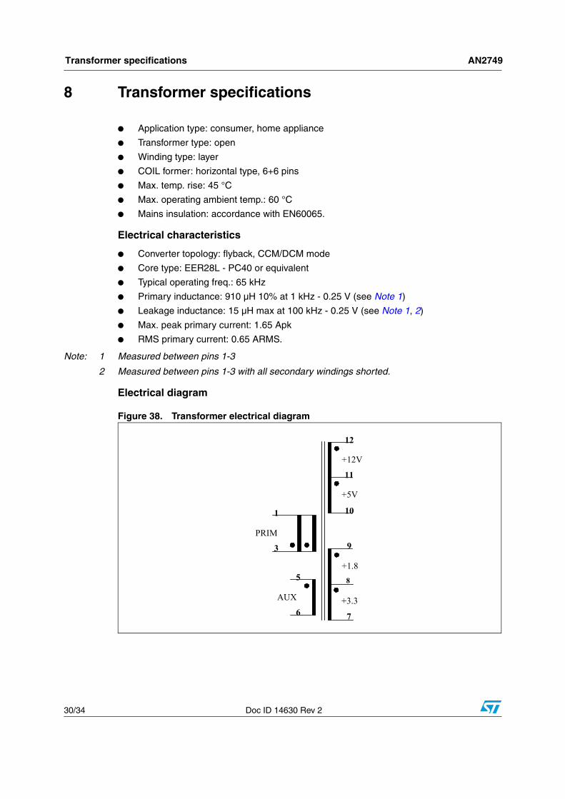
Figure 38. Transformer electrical diagram
1
3
PRIM
5
6
AUX
+1.8
7
+3.3
10
9
11
+5V
12
+12V
8

AN2749 Transformer specifications
Doc ID 14630 Rev 2 31/34
Figure 39. Transformer winding diagram
Mechanical aspect
● Maximum height from PCB: 30 mm
● Coil former type: horizontal, 6+6 pins (pins 2, 4 are removed)
● Pin distance: 5 mm
● Row distance: 30 mm
● Pins #3 and 4 removed
● External copper shield: 12 mm width
Manufacturer
● TDK Electronics Europe - Germany
● Transformer P/N: SRW28LEC-E01H117
Table 9. Transformer winding characteristics
Pins Winding O/P RMS current Number of turns Wire type
3-1 PRIMARY - A 0.32 ARMS 95 G2 – 2 x φ 0.23 mm
12-11 12 V 2.3 ARMS 9 G2 – 3 x φ 0.45 mm
11-10 5 V 3 ARMS 7 spaced G2 – 3 x φ 0.45 mm
9-8 3.3 V 0.6 ARMS 2 G2 – 3 x φ 0.45 mm
8-7 1.8 V 2.1 ARMS 3 G2 – 3 x φ 0.45 mm
3-1 PRIMARY - B 0.32 ARMS 95 G2– 2 x φ 0.23 mm
5-6 AUX 0.05 ARMS 17 spaced G2 – φ 0.23 mm

Conclusion AN2749
32/34 Doc ID 14630 Rev 2
9 Conclusion
An SMPS for set-top box has been completely designed and tested, with positive results from all aspects (functionality, protections, EMI and component thermal stress). Thanks to the L6566B, the design offers high performance at low cost which is a key driver in the consumer electronics market.
9.1 References1. "L6566B datasheet".

AN2749 Revision history
Doc ID 14630 Rev 2 33/34
10 Revision history
Table 10. Document revision history
Date Revision Changes
23-Jul-2008 1 Initial release
08-Jun-2010 2 Modified: Figure 11, 34 and 35

AN2749
34/34 Doc ID 14630 Rev 2
Please Read Carefully:
Information in this document is provided solely in connection with ST products. STMicroelectronics NV and its subsidiaries (“ST”) reserve theright to make changes, corrections, modifications or improvements, to this document, and the products and services described herein at anytime, without notice.
All ST products are sold pursuant to ST’s terms and conditions of sale.
Purchasers are solely responsible for the choice, selection and use of the ST products and services described herein, and ST assumes noliability whatsoever relating to the choice, selection or use of the ST products and services described herein.
No license, express or implied, by estoppel or otherwise, to any intellectual property rights is granted under this document. If any part of thisdocument refers to any third party products or services it shall not be deemed a license grant by ST for the use of such third party productsor services, or any intellectual property contained therein or considered as a warranty covering the use in any manner whatsoever of suchthird party products or services or any intellectual property contained therein.
UNLESS OTHERWISE SET FORTH IN ST’S TERMS AND CONDITIONS OF SALE ST DISCLAIMS ANY EXPRESS OR IMPLIEDWARRANTY WITH RESPECT TO THE USE AND/OR SALE OF ST PRODUCTS INCLUDING WITHOUT LIMITATION IMPLIEDWARRANTIES OF MERCHANTABILITY, FITNESS FOR A PARTICULAR PURPOSE (AND THEIR EQUIVALENTS UNDER THE LAWSOF ANY JURISDICTION), OR INFRINGEMENT OF ANY PATENT, COPYRIGHT OR OTHER INTELLECTUAL PROPERTY RIGHT.
UNLESS EXPRESSLY APPROVED IN WRITING BY AN AUTHORIZED ST REPRESENTATIVE, ST PRODUCTS ARE NOTRECOMMENDED, AUTHORIZED OR WARRANTED FOR USE IN MILITARY, AIR CRAFT, SPACE, LIFE SAVING, OR LIFE SUSTAININGAPPLICATIONS, NOR IN PRODUCTS OR SYSTEMS WHERE FAILURE OR MALFUNCTION MAY RESULT IN PERSONAL INJURY,DEATH, OR SEVERE PROPERTY OR ENVIRONMENTAL DAMAGE. ST PRODUCTS WHICH ARE NOT SPECIFIED AS "AUTOMOTIVEGRADE" MAY ONLY BE USED IN AUTOMOTIVE APPLICATIONS AT USER’S OWN RISK.
Resale of ST products with provisions different from the statements and/or technical features set forth in this document shall immediately voidany warranty granted by ST for the ST product or service described herein and shall not create or extend in any manner whatsoever, anyliability of ST.
ST and the ST logo are trademarks or registered trademarks of ST in various countries.
Information in this document supersedes and replaces all information previously supplied.
The ST logo is a registered trademark of STMicroelectronics. All other names are the property of their respective owners.
© 2010 STMicroelectronics - All rights reserved
STMicroelectronics group of companies
Australia - Belgium - Brazil - Canada - China - Czech Republic - Finland - France - Germany - Hong Kong - India - Israel - Italy - Japan - Malaysia - Malta - Morocco - Philippines - Singapore - Spain - Sweden - Switzerland - United Kingdom - United States of America
www.st.com