The Flyback Converter -...
7
The Flyback Converter Course Project Power Electronics Design and Implementation Report by Kamran Ali 13100174 Muhammad Asad Lodhi 13100175 Ovais bin Usman 13100026 Syed Bilal Ali 13100026 Advisor Nauman Zaffar [[email protected]@lums.edu.pk] Reader January 13, 2013 Department of Electrical Engineering Syed Babar Ali School of Science and Engineering Lahore University of Management Sciences, Pakistan
Transcript of The Flyback Converter -...

The Flyback Converter
Course ProjectPower Electronics
Design and Implementation Report
byKamran Ali 13100174
Muhammad Asad Lodhi 13100175Ovais bin Usman 13100026
Syed Bilal Ali 13100026
AdvisorNauman Zaffar
[[email protected]@lums.edu.pk]
Reader
January 13, 2013Department of Electrical Engineering
Syed Babar Ali School of Science and EngineeringLahore University of Management Sciences, Pakistan
Contents
1 Introduction and Derivation 1
2 Analysis of the flyback converter 1
3 Design Specifications 3
4 Design 3
5 Implementation 4
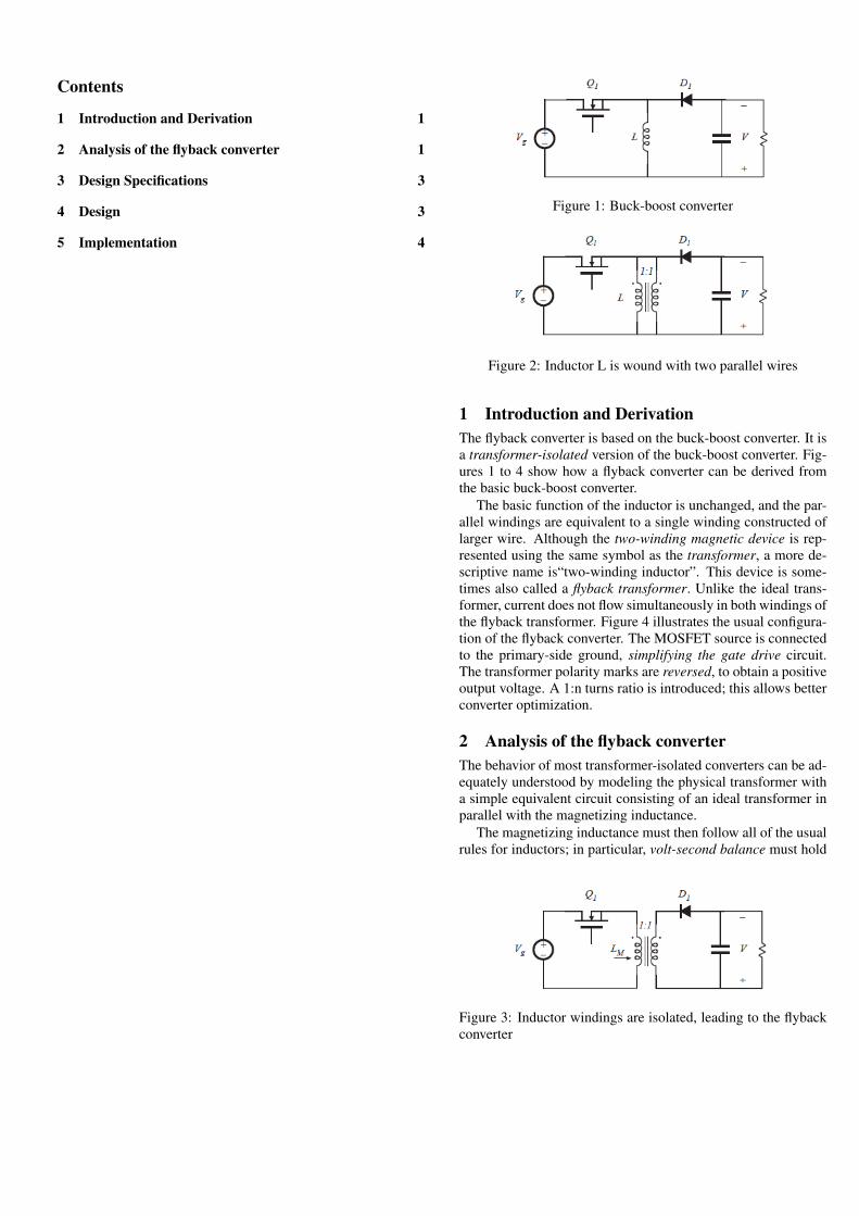
Figure 1: Buck-boost converter
Figure 2: Inductor L is wound with two parallel wires
1 Introduction and DerivationThe flyback converter is based on the buck-boost converter. It isa transformer-isolated version of the buck-boost converter. Fig-ures 1 to 4 show how a flyback converter can be derived fromthe basic buck-boost converter.
The basic function of the inductor is unchanged, and the par-allel windings are equivalent to a single winding constructed oflarger wire. Although the two-winding magnetic device is rep-resented using the same symbol as the transformer, a more de-scriptive name is“two-winding inductor”. This device is some-times also called a flyback transformer. Unlike the ideal trans-former, current does not flow simultaneously in both windings ofthe flyback transformer. Figure 4 illustrates the usual configura-tion of the flyback converter. The MOSFET source is connectedto the primary-side ground, simplifying the gate drive circuit.The transformer polarity marks are reversed, to obtain a positiveoutput voltage. A 1:n turns ratio is introduced; this allows betterconverter optimization.
2 Analysis of the flyback converterThe behavior of most transformer-isolated converters can be ad-equately understood by modeling the physical transformer witha simple equivalent circuit consisting of an ideal transformer inparallel with the magnetizing inductance.
The magnetizing inductance must then follow all of the usualrules for inductors; in particular, volt-second balance must hold
Figure 3: Inductor windings are isolated, leading to the flybackconverter

Figure 4: With a 1:n turns ratio and positive output
Figure 5: With transformer equivalent circuit models
when the circuit operates in steady-state. This implies that theaverage voltage applied across every winding of the transformermust be zero.
Application of the principle of volt-second balance to theprimary-side magnetizing inductance yields
〈vL〉 = D(Vg) +D′(−V
n)
M(D) =n2D
n1(1−D)
where we have taken transformer’s turn ratio n = n1/n2.Similarly, application of the principle of charge balance to
the output capacitor C leads to
〈iC〉 = D(−VR
) +D′(I
n− V
R)
Im =n2V
n1RD′
where Im represents the dc component of the magnetizingcurrent, referred to the primary. The dc component of the sourcecurrent ig is
Ig = DI
Figures 5-8 show the process through which we arrived toabove results. Figure 9 shows the equivalent circuit which mod-els the dc components of the flyback converter waveforms canbe constructed. It contains a 1:D buck-type conversion ratio, fol-lowed by a (1−D):1 boost-type conversion ratio, and an addedfactor of 1:n, arising from the flyback transformer turns ratio.
After taking the stress on the transistor (the active switchingcomponent) and Pload into account, the Utilization factor of this
Figure 6: During subinterval 1
Figure 7: During subinterval 2
Figure 8: Flyback converter waveforms, continuous conductionmode

Figure 9: Flyback converter equivalent circuit models
converter comes out to be
U =PloadStotal
Uflyback =√D(1−D)
The flyback converter is commonly used at the 50−100W powerrange, as well as in high voltage power supplies for televisionsand computer monitors. It has the advantage of very low partscount. Multiple outputs can be obtained using a minimum num-ber of parts: each additional output requires only an additionalwinding, diode, and capacitor. The peak transistor voltage isequal to the dc input voltage Vg plus the reflected load voltageV/n; in practice, additional voltage is observed due to ringingassociated with the transformer leakage inductance. A snub-ber circuit may be required to clamp the magnitude of this ring-ing voltage to a safe level that is within the peak voltage ratingof the transistor [1].
3 Design SpecificationsFollowing are our design specifications1) Output voltage (Vout) =12 Volts2) Input Voltage (Vin) =332 Volts3) Max Output Power = 50 Watts4) Output Voltage ripple (∆Vout) = 0.1 Volts5) Switching frequency (fs) = 40 KHz
4 Design• First we find that value of ’D’ , the duty cycle which max-
imizes the Utilization factor. Utilization factor for flybackconverter is U =
√D(1 −D), from this equation we find
the value of ’D’ which maximizes the utilization, whichcomes out to be D = 1
3 .
• Next we find the desired turns ratio using M(D). Pluggingin Vout =12 Volts , Vin = 332 Volts and D=1/3 we get
n =6
83
• Finding the Load resistance value.
Pout =V 2out
R
Plugging in the Vout = 12 Volts and Pout = 50 Watts,
R =V 2out
Pout
R = 2.88 Ω
• Finding the Value of Capacitance. Plugging in the Vout =12 Volts, D = 1/3, Ts = 1/fs, R= 2.88 Ω, and ∆Vout = 0.1Volts we get,
C =VoutDTs2R∆vout
C = 69.4 uF
We can use a value greater than this too but not smaller.
• Finding the value of Inductance (L): For the calculation ofinductance, we first need to calculate a couple of thingswhich are: Im, ∆im, Im,max, I1, I2, and Itot.
The Im is calculated as:
Im =n2V
n1RD′
Plugging the values in the above formula, we get:
Im = 5/12 = 0.4167 A
∆im is kept to be 20% of Im. So, the value of ∆im we getis:
∆im = 1/12 A
Im,max is the sum of Im and ∆im.
I1 is calculated by the formula
I1 = Im√D
√1 +
1
3
(∆imIm
)2
Plugging in the required values in the above formula, weget:
I1 = 0.242 A
I2 is calculated by the formula
I2 =n1n2Im√D′
√1 +
1
3
(∆imIm
)2
Plugging the values in the above formula, we get:
I2 = 5.137 A
Itot is calculated by:
Itotal = I1 +n2n1I1
Plugging the values in the above formula, we get:
Itot = 0.5846 A

• inding the value of core parameters: We now need to findsome of the parameters of the core:1) Mean Length per turn (MLT)2) Cross-Sectional area of wire3) Winding area4) Length of the air gap5) Number of turns of the primary winding6) Number of turns of the secondary winding7) Fraction of window area allocation8) Window area of a specific winding
The mean length per turn is calculated by finding the cir-cumference of the core on which the windings are to bewound. In our case, it came out to be:
MLT = 2(1.245 + 1.535) cm
MLT = 5.56 cm
The cross sectional area is the area of the core on whichthe winding is to be wound. In our case, it came out to be:
Ac = (0.97× 1.26) cm2
Ac = 1.22 cm2
The winding area is the total area in which the windingswill be placed. We are using EI-core, thus the total wind-ing area is:
WA = 2(1.965× 0.795) cm2
WA = 3.124 cm2
The air gap is found by formula:
lg =µ0LmI
2m,max
AcB2max
104
lg = 0.683 mm
The number of primary windings is calculated as:
n1 =LmIm,maxAcBmax
104
n1 = 271.64
The number of secondary windings is calculated as:
n2 =n2n1n1
n2 = 19.63
The fraction of window allocation is calculated by the fol-lowing formula:
αj =njIjn1Itot
α1 = 41.4%
α2 = 58.6%
Figure 10: PCB Design
Figure 11: Protection Circuit with breaker and bulb
• The wire sizes are calculated as:
Aw,k =αkKµWA
nk
Aw,1 ≤ 1.4285× 10⁻³
Aw,2 ≤ 19.7× 10⁻³
The A′
ws are then matched from a table to get the gauge ofthe wire to be used.
Gauge1 ≥ 26
Gauge2 ≥ 15
We used following gauge wires available in the lab. Theymeet the above requirements.
Gauge1 = 28
Gauge2 = 18
5 ImplementationFigure 10 shows the PCB we designed. It includes the Recti-fier, Gate Derive Circuit and the main Flyback converter com-ponents. Moreover, figures 11 to 21 show implemented circuitsand oscilloscope outputs (showing significant characteristics ofthe converter e.g. voltage across the active switch Q1 IGBT)
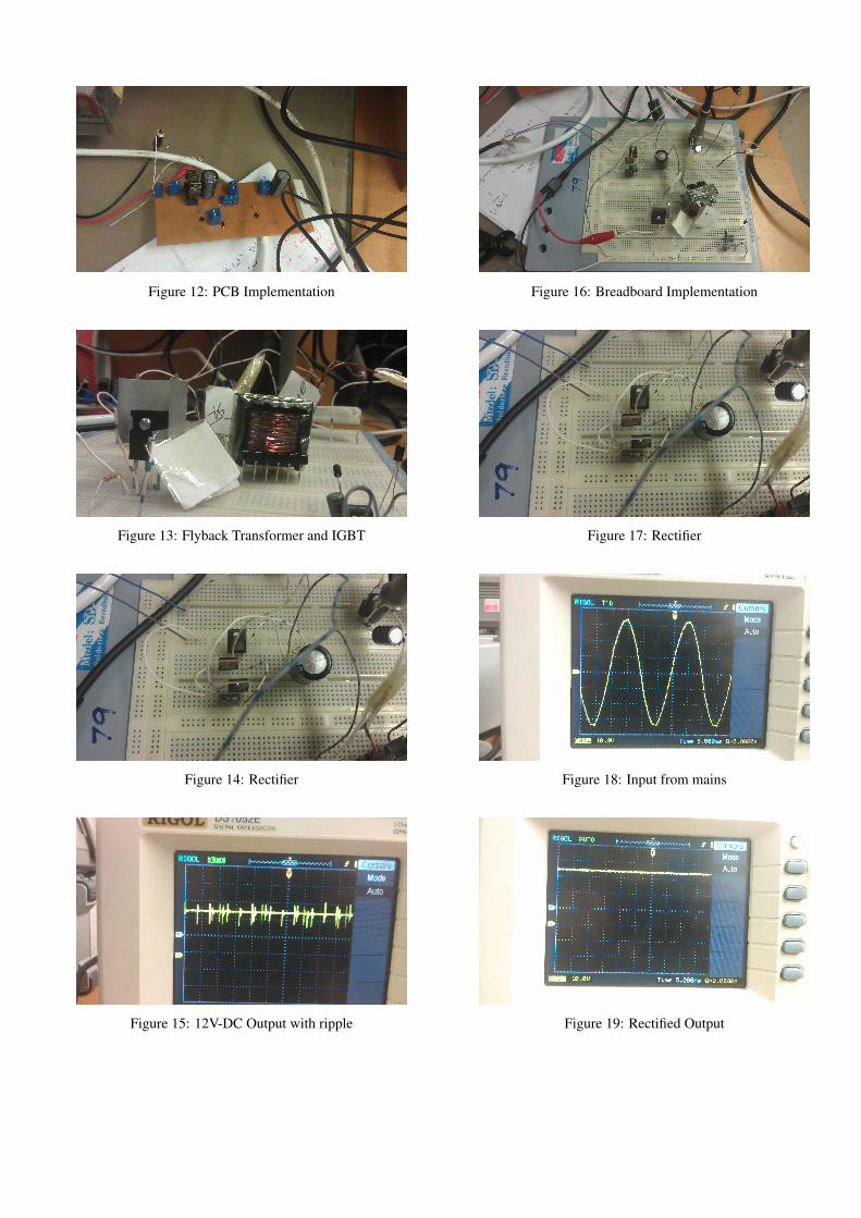
Figure 12: PCB Implementation
Figure 13: Flyback Transformer and IGBT
Figure 14: Rectifier
Figure 15: 12V-DC Output with ripple
Figure 16: Breadboard Implementation
Figure 17: Rectifier
Figure 18: Input from mains
Figure 19: Rectified Output

Figure 20: Voltage blocked by IGBT
Figure 21: Ringing effect due to the leakage inductance of trans-former
References[1] ecee.colorado.edu/ ecen4517/materials/flyback.pdf
[2] R. W. Erickson: Fundamentals of Power Electronics