35-75V 48V 3Amp 2000Vdc Quarter-brick - SynQor | SynQor
13
T T echnical echnical S S pecification pecification PQ60480QT PQ60480QTA03 A03 Product # PQ60480QTA03 Phone 1-888-567-9596 www .synqor .com Doc.# 005-2QT648C Rev. B 12/16/19 Page 1 35-75V 35-75V 48V 48V 3Amp 3Amp 2000Vdc 2000Vdc Quar Quar ter-brick ter-brick Input Input Output Output Current Current Isolation Isolation DC/DC Conver DC/DC Conver ter ter • Ultra-high efficiency, 92% at full rated load current • Delivers up to 3 amps of output current (144W) with minimal derating - no heatsink required • Wide input voltage range: 35V – 75V, with 100V 100ms input voltage transient capability • Fixed frequency switching provides predictable EMI per- formance • No minimum load requirement means no preload resis- tors required Operational Features Operational Features • Input under-voltage lockout disables converter at low input voltage conditions • Output current limit and short circuit protection protects converter and load from permanent damage and conse- quent hazardous conditions • Active back bias limit prevents damage to converter from external load induced pre-bias • Output over-voltage protection protects load from dam- aging voltages • Thermal shutdown protects converter from abnormal environmental conditions Pr Pr otection Features otection Features • 2000V, 30 MW input-to-output isolation provides input/output ground separation • UL/cUL 60950-1 recognized (US & Canada), basic insulation rating • TUV certified to EN60950-1 • Meets 72/23/EEC and 93/68/EEC directives which facilitates CE Marking in user’s end product • Board and plastic components meet UL94V-0 flammabil- ity requirements Safety Features Safety Features • Industry standard quarter-brick pin-out configuration • Industry standard size: 1.45” x 2.3” (36.8x58.4mm) • Total height less than 0.43” (10.9mm), permits better airflow and smaller card pitch • Total weight: 1.5 oz. (42 grams) • Flanged pins designed to permit surface mount soldering (allows to avoiding wave solder) using FPiP technique Mechanical Features Mechanical Features • On/Off control referenced to input side (positive and negative logic options are available) • Remote sense for the output voltage compensates for output distribution drops • Output voltage trim permits custom voltages and voltage margining Contr Contr ol Features ol Features PQ60480QTA03 Module The PQ60048QTA03 PowerQor ® Tera converter is a next- generation, board-mountable, isolated, DC-DC converter that uses synchronous rectification to achieve extremely high conversion efficiency. The power dissipated by the converter is so low that a heatsink is not required, which saves cost, weight, height, and application effort. All of the power and control components are mounted to the multi-layer PCB substrate with high-yield surface mount technology. Since the PowerQor converter has no explicit thermal interfaces, it is extremely reliable. The Tera series offers the maximum usable output current for any standard "quarter-brick" module. RoHS 6/6 compliant (see page 13).
Transcript of 35-75V 48V 3Amp 2000Vdc Quarter-brick - SynQor | SynQor

TTechnicalechnicalSSpecificationpecificationPQ60480QTPQ60480QTA03A03
Product # PQ60480QTA03 Phone 1-888-567-9596 www.synqor.com Doc.# 005-2QT648C Rev. B 12/16/19 Page 1
35-75V35-75V 48V48V 3Amp3Amp 2000Vdc2000Vdc QuarQuarter-brick ter-brick InputInput OutputOutput CurrentCurrent IsolationIsolation DC/DC ConverDC/DC Converterter
• Ultra-high efficiency, 92% at full rated load current• Delivers up to 3 amps of output current (144W) with
minimal derating - no heatsink required• Wide input voltage range: 35V – 75V, with 100V
100ms input voltage transient capability• Fixed frequency switching provides predictable EMI per-
formance• No minimum load requirement means no preload resis-
tors required
Operational FeaturesOperational Features
• Input under-voltage lockout disables converter at lowinput voltage conditions
• Output current limit and short circuit protection protectsconverter and load from permanent damage and conse-quent hazardous conditions
• Active back bias limit prevents damage to converterfrom external load induced pre-bias
• Output over-voltage protection protects load from dam-aging voltages
• Thermal shutdown protects converter from abnormalenvironmental conditions
PrProtection Featuresotection Features
• 2000V, 30 MΩ input-to-output isolation providesinput/output ground separation
• UL/cUL 60950-1 recognized (US & Canada), basicinsulation rating
• TUV certified to EN60950-1• Meets 72/23/EEC and 93/68/EEC directives which
facilitates CE Marking in user’s end product• Board and plastic components meet UL94V-0 flammabil-
ity requirements
Safety FeaturesSafety Features
• Industry standard quarter-brick pin-out configuration• Industry standard size: 1.45” x 2.3” (36.8x58.4mm)• Total height less than 0.43” (10.9mm), permits better
airflow and smaller card pitch• Total weight: 1.5 oz. (42 grams)• Flanged pins designed to permit surface mount soldering
(allows to avoiding wave solder) using FPiP technique
Mechanical FeaturesMechanical Features
• On/Off control referenced to input side (positive andnegative logic options are available)
• Remote sense for the output voltage compensates foroutput distribution drops
• Output voltage trim permits custom voltages and voltagemargining
ContrControl Featuresol Features
PQ60480QTA03 Module
The PQ60048QTA03 PowerQor® Tera converter is a next-generation, board-mountable, isolated, DC-DC converter that uses synchronous rectification to achieve extremely high conversion efficiency. The power dissipated by the converter is so low that a heatsink is not required, which saves cost, weight, height, and application effort. All of the power and control components are mounted to the multi-layer PCB substrate with high-yield surface mount technology. Since the PowerQor converter has no explicit thermal interfaces, it is extremely reliable. The Tera series offers the maximum usable output current for any standard "quarter-brick" module. RoHS 6/6 compliant (see page 13).

0.300(7.62)
0.600(15.24)
1.45(36.8)
0.43(10.9)
0.150(3.81)
0.300(7.62)
0.450(11.43) 0.600
(15.24)
0.14(3.6)
2.30(58.4)
2.00(50.8)
Top View
Side ViewLoad Board
Bottom sideClearanceSee Note 9
LowestComponent
0.43(10.9)
0.060+.022/-.032(1.52+.56/-.81)
0.145 (3.68)
See Note 3
Flanged PinSee Note 10
Input:Input:Output:Output:
Current:Current:PPackage:ackage:
35-75 V35-75 V48 V48 V3 A 3 A (144W)(144W)Quarter-brickQuarter-brickTTechnical Sechnical Specificationpecification
Product # PQ60480QTA03 Phone 1-888-567-9596 www.synqor.com Doc.# 005-2QT648C Rev. B 12/16/19 Page 2
MECHANICAL DIAGRAM
NOTES1) Pins 1-3, 5-7 are 0.040” (1.02mm) diameter with
0.080” (2.03 mm) diameter standoff shoulders.2) Pins 4 and 8 are 0.062” (1.57 mm) diameter with 0.100”
(2.54 mm) diameter standoff shoulders.3) Other pin extension lengths available. Recommended pin
length is 0.03” (0.76mm) greater than the PCB thickness.4) All Pins: Material - Copper Alloy
Finish (RoHS 6/6) - Matte Tin over Nickel plate5) Undimensioned components are shown for visual reference only.6) All dimensions in inches (mm)
Tolerances: x.xx +0.02 in. (x.x +0.5mm)x.xxx +0.010 in. (x.xx +0.25mm)
7) Weight: 1.5 oz. (42 g) typical8) Workmanship: Meets or exceeds IPC-A-610C Class II9) UL/TUV standards require a clearance greater than 0.04”
(1.02mm) between input and output for basic insulation. This issueshould be considered if any copper traces are on the top side of theuser’s board. Note that the ferrite cores are considered part of theinput/primary circuit.
10) The flanged pins are designed to permit surface mount solder-ing (allowing to avoid the wave soldering process) through theuse of the flanged pin-in-paste technique.
Pin No. Name Function1 Vin(+) Positive input voltage2 ON/OFF TTL input to turn converter
on and off, referenced to Vin(–), with internal pull up.
3 Vin(–) Negative input voltage4 Vout(–) Negative output voltage5 SENSE(–) Negative remote sense1
6 TRIM Output voltage trim2
7 SENSE(+) Positive remote sense3
8 Vout(+) Positive output voltage
Notes:
1. SENSE(–) should be connected to Vout(–) either remotely or at the converter.
2. Leave TRIM pin open for nominal output voltage.
3. SENSE(+) should be connected to Vout(+) either remotely or at the converter.
PIN DESIGNATIONS

Input:Input:Output:Output:
Current:Current:PPackage:ackage:
35-75 V35-75 V48 V48 V3 A 3 A (144W)(144W)Quarter-brickQuarter-brickTTechnical Sechnical Specificationpecification
Product # PQ60480QTA03 Phone 1-888-567-9596 www.synqor.com Doc.# 005-2QT648C Rev. B 12/16/19 Page 3
Parameter Min. Typ. Max. Units Notes & ConditionsABSOLUTE MAXIMUM RATINGSInput Voltage
Non-Operating 100 V ContinuousOperating 80 V ContinuousOperating Transient Protection 100 V 100ms transient, square wave
Isolation Voltage (input to output) 2000 V Basic insulation, Pollution Degree 2Operating Temperature -40 100 °CStorage Temperature -55 125 °CVoltage at ON/OFF input pin -2 18 VINPUT CHARACTERISTICSOperating Input Voltage Range 35 48 75 V 100V transient for 100msInput Under-Voltage Lockout
Turn-On Voltage Threshold 31.5 32.5 34.0 VTurn-Off Voltage Threshold 28.7 29.5 31.2 VLockout Voltage Hysteresis 2.5 3.5 4.5 V
Maximum Input Current 5.1 A 100% Load, 35 Vin, trimmed up 5%No-Load Input Current 120 150 mADisabled Input Current 2 5 mA
Inrush Current Transient Rating 0.01 A2sResponse to Input Transient 1 V 1000V/ms input transientInput Reflected Ripple Current 13 mA P-P thru 10µH inductor; Figures 13 & 15Input Terminal Ripple Current 40 mA RMS; Figures 13 & 14Recommended Input Fuse 20 A Fast blow external fuse recommendedInput Filter Component Values (L\C) 3.3\6.6 µH\µF Internal values; Figure E (Lin\C2)Recommended External Input Capacitance 47 µF Typical ESR 0.1-0.2Ω; Figure 13OUTPUT CHARACTERISTICSOutput Voltage Set Point 47.4 48.00 48.6 VOutput Voltage Regulation
Over Line1 +0.02\10 +0.1\48 %\mVOver Load1 +0.02\10 +0.1\48 %\mVOver Temperature +288 +400 mV
Total Output Voltage Range 46.9 49.1 V Over sample, line, load, temperature & lifeOutput Voltage Ripple and Noise2 500MHz bandwidth; Figures 13 & 16
Peak-to-Peak 12 150 mV Full Load; Figures 13 & 16RMS 5 60 mV Full Load; Figures 13 & 16
Operating Output Current Range 0 3 A Subject to thermal derating; Figures 5 - 8Output DC Current-Limit Inception 3.5 3.8 4.4 A Output Voltage 10% LowOutput DC Current-Limit Shutdown Voltage 19 VBack-Drive Current Limit while Enabled 0.1 0.3 0.8 A Negative current drawn from output sourceBack-Drive Current Limit while Disabled 0 30 55 mA Negative current drawn from output sourceMaximum Output Capacitance 688 µF 48Vout at 3A Resistive LoadDYNAMIC CHARACTERISTICSInput Voltage Ripple Rejection 20 dB 120 Hz; Figure 20Output Voltage during Load Current Transient
For a Step Change in Output Current (0.1A/µs) 2 V 50% to 75% to 50% Iout maxSettling Time 500 µs To within 1% Vout nom
Turn-On TransientTurn-On Time 33 ms Full load, ON/OFF to Vout=90% nom.; Figures 9 - 10Start-Up Inhibit Time 230 250 270 ms -40°C to +125°C; Figure EOutput Voltage Overshoot 0 % 688 µF load capacitance, Iout = 0A
EFFICIENCY100% Load 92 % Figures 1 & 250% Load 92 % Figures 1 & 2TEMPERATURE LIMITS FOR POWER DERATING CURVESSemiconductor Junction Temperature 125 °C Package rated to 150°CBoard Temperature 125 °C UL rated max operating temp 130°CTransformer Temperature 125 °C See Figures 5 - 8 for derating curvesISOLATION CHARACTERISTICSIsolation Voltage (dielectric strength) 2000 VIsolation Resistance 30 MΩIsolation Capacitance3 470 pF
PQ60480QTA03 ELECTRICAL CHARACTERISTICS TA=25°C, airflow rate=300 LFM, Vin=48Vdc unless otherwise noted; full operating temperature range is -40°C to +100°C ambient tem-perature with appropriate power derating. Specifications subject to change without notice.
Note 1: Line and load regulation is limited by duty cycle quantization and does not indicate a shift in the internal voltage reference.Note 2: For applications requiring reduced output voltage ripple and noise, consult SynQor applications support (e-mail: [email protected]).Note 3: Higher values of isolation capacitance can be added external to the module.
Input:Input:Output:Output:
Current:Current:PPackage:ackage:
35-75 V35-75 V48 V48 V3 A 3 A (144W)(144W)Quarter-brickQuarter-brickTTechnical Sechnical Specificationpecification
Product # PQ60480QTA03 Phone 1-888-567-9596 www.synqor.com Doc.# 005-2QT648C Rev. B 12/16/19 Page 4
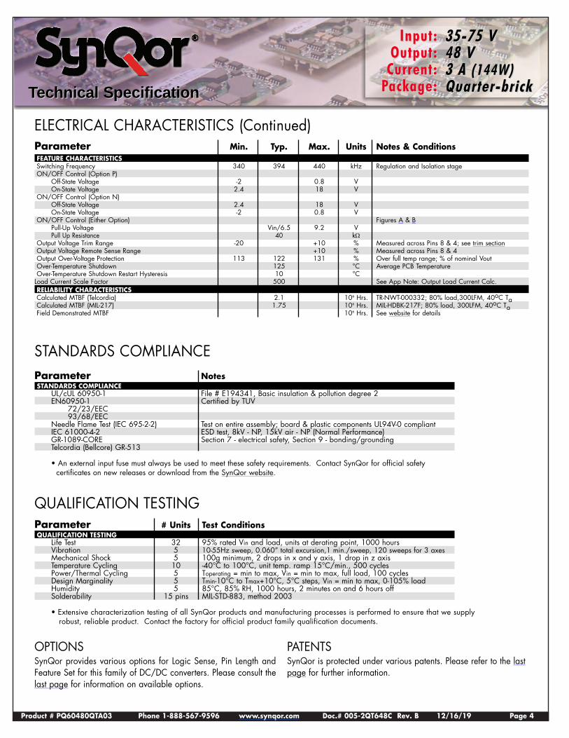
ELECTRICAL CHARACTERISTICS (Continued)ParameterP Min. Typ. Max. Units Notes & ConditionsFEATURE CHARACTERISTICSSwitching Frequency 340 394 440 kHz Regulation and Isolation stageON/OFF Control (Option P)
Off-State Voltage -2 0.8 VOn-State Voltage 2.4 18 V
ON/OFF Control (Option N)Off-State Voltage 2.4 18 VOn-State Voltage -2 0.8 V
ON/OFF Control (Either Option) Figures A & BPull-Up Voltage Vin/6.5 9.2 VPull Up Resistance 40 kΩ
Output Voltage Trim Range -20 +10 % Measured across Pins 8 & 4; see trim sectionOutput Voltage Remote Sense Range +10 % Measured across Pins 8 & 4Output Over-Voltage Protection 113 122 131 % Over full temp range; % of nominal VoutOver-Temperature Shutdown 125 °C Average PCB TemperatureOver-Temperature Shutdown Restart Hysteresis 10 °C
Load Current Scale Factor 500 See App Note: Output Load Current Calc.RELIABILITY CHARACTERISTICSCalculated MTBF (Telcordia) 2.1 106 Hrs. TR-NWT-000332; 80% load,300LFM, 40oC TaCalculated MTBF (MIL-217) 1.75 106 Hrs. MIL-HDBK-217F; 80% load, 300LFM, 40oC TaField Demonstrated MTBF 106 Hrs. See website for details
STANDARDS COMPLIANCEParameterP NotesSTANDARDS COMPLIANCE
UL/cUL 60950-1 File # E194341, Basic insulation & pollution degree 2EN60950-1 Certified by TUV
72/23/EEC93/68/EEC
Needle Flame Test (IEC 695-2-2) Test on entire assembly; board & plastic components UL94V-0 compliantIEC 61000-4-2 ESD test, 8kV - NP, 15kV air - NP (Normal Performance)GR-1089-CORE Section 7 - electrical safety, Section 9 - bonding/groundingTelcordia (Bellcore) GR-513
• An external input fuse must always be used to meet these safety requirements. Contact SynQor for official safetycertificates on new releases or download from the SynQor website.
QUALIFICATION TESTINGParameterP # Units Test ConditionsQUALIFICATION TESTING
Life Test 32 95% rated Vin and load, units at derating point, 1000 hoursVibration 5 10-55Hz sweep, 0.060” total excursion,1 min./sweep, 120 sweeps for 3 axesMechanical Shock 5 100g minimum, 2 drops in x and y axis, 1 drop in z axisTemperature Cycling 10 -40°C to 100°C, unit temp. ramp 15°C/min., 500 cyclesPower/Thermal Cycling 5 Toperating = min to max, Vin = min to max, full load, 100 cyclesDesign Marginality 5 Tmin-10°C to Tmax+10°C, 5°C steps, Vin = min to max, 0-105% loadHumidity 5 85°C, 85% RH, 1000 hours, 2 minutes on and 6 hours offSolderability 15 pins MIL-STD-883, method 2003
• Extensive characterization testing of all SynQor products and manufacturing processes is performed to ensure that we supplyrobust, reliable product. Contact the factory for official product family qualification documents.
OPTIONSSynQor provides various options for Logic Sense, Pin Length andFeature Set for this family of DC/DC converters. Please consult thelast page for information on available options.
PATENTSSynQor is protected under various patents. Please refer to the lastpage for further information.

Input:Input:Output:Output:
Current:Current:PPackage:ackage:
35-75 V35-75 V48 V48 V3 A 3 A (144W)(144W)Quarter-brickQuarter-brickTTechnical Sechnical Specificationpecification
Product # PQ60480QTA03 Phone 1-888-567-9596 www.synqor.com Doc.# 005-2QT648C Rev. B 12/16/19 Page 5
86
88
90
92
94
96
98
100 200 300 400Air Flow (LFM)
Effic
ienc
y (%
)
25º C40º C55º C
4
5
6
7
8
9
10
100 200 300 400Air Flow (LFM)
Pow
er D
issi
patio
n (W
)
25º C40º C55º C
60
65
70
75
80
85
90
95
100
0.0 0.5 1.0 1.5 2.0 2.5 3.0Load Current (A)
Effic
ienc
y (%
)
35 Vin48 Vin75 Vin
Figure 1: Efficiency at nominal output voltage vs. load current for min-imum, nominal, and maximum input voltage at 25°C.
Figure 2: Efficiency at nominal output voltage and 60% rated power vs.airflow rate for ambient air temperatures of 25°C, 40°C, and 55°C(nominal input voltage).
0
2
4
6
8
10
12
14
0.0 0.5 1.0 1.5 2.0 2.5 3.0Load Current (A)
Pow
er D
issi
patio
n (W
)
35 Vin48 Vin75 Vin
Figure 3: Power dissipation at nominal output voltage vs. load currentfor minimum, nominal, and maximum input voltage at 25°C.
Figure 4: Power dissipation at nominal output voltage and 60% ratedpower vs. airflow rate for ambient air temperatures of 25°C, 40°C, and55°C (nominal input voltage).
0.0
0.5
1.0
1.5
2.0
2.5
3.0
3.5
25 40 55 70 85Ambient Air Temperature (°C)
Iout
(A)
400 LFM (2.0 m/s)300 LFM (1.5 m/s)200 LFM (1.0 m/s)100 LFM (0.5 m/s)
Figure 5: Maximum output power derating curves vs. ambient air tem-perature for airflow rates of 100 LFM through 400 LFM with air flow-ing across the converter from input to output (nominal input voltage).
Figure 6: Thermal plot of converter at 3 amp load current (144W) with55°C air flowing at the rate of 200 LFM. Air is flowing across the con-verter from input to output (nominal input voltage).
Semiconductor junction temperature iswithin 1°C of surface temperature

Input:Input:Output:Output:
Current:Current:PPackage:ackage:
35-75 V35-75 V48 V48 V3 A 3 A (144W)(144W)Quarter-brickQuarter-brickTTechnical Sechnical Specificationpecification
Product # PQ60480QTA03 Phone 1-888-567-9596 www.synqor.com Doc.# 005-2QT648C Rev. B 12/16/19 Page 6
0
2
4
6
8
10
12
40.0 39.5 39.0 38.5 38.0 37.5 37.0 36.6 36.0 35.5 35.0
Input Voltage (V)
Vout
Trim
-up
(%)
100% Load50% Load0% Load
Figure 12: Percentage of output voltage trim-up that can be achieved atvarious input voltages from Vin 35V-40V and output loads of 0%, 50%and full load.
0.0
0.5
1.0
1.5
2.0
2.5
3.0
3.5
25 40 55 70 85Ambient Air Temperature (°C)
Iout
(A)
400 LFM (2.0 m/s)300 LFM (1.5 m/s)200 LFM (1.0 m/s)100 LFM (0.5 m/s)
Figure 7: Maximum output power derating curves vs. ambient air tem-perature for airflow rates of 100 LFM through 400 LFM with air flow-ing from pin 1 to pin 3 (nominal input voltage).
Figure 8: Thermal plot of converter at 3 amp load current (144W) with55°C air flowing at the rate of 200 LFM. Air is flowing from pin 3 topin 1 (nominal input voltage).
Figure 9: Turn-on transient at full rated load (resistive load) (20ms/div) Input voltage pre-applied. Ch 1: Vout (20V/div). Ch 2:ON/OFF input (5V/div)
Figure 10: Turn-on transient at zero load current (5 ms/div).Ch 1: Vout (20V/div)Ch 2: ON/OFF input (5V/div)
Figure 11: Output voltage response to step-change in load current (50%-75%-50% of Iout(max); dI/dt = 0.1A/µ s). Load cap: 10µ F, 100 mΩ ESR tantalumcapacitor and 1µ F ceramic capacitor. Ch 1: Vout (2V/div), Ch 2: Iout (2A/div).
Semiconductor junction temperature iswithin 1°C of surface temperature

Input:Input:Output:Output:
Current:Current:PPackage:ackage:
35-75 V35-75 V48 V48 V3 A 3 A (144W)(144W)Quarter-brickQuarter-brickTTechnical Sechnical Specificationpecification
Product # PQ60480QTA03 Phone 1-888-567-9596 www.synqor.com Doc.# 005-2QT648C Rev. B 12/16/19 Page 7
Figure 14: Input Terminal Ripple Current, ic, at full rated output cur-rent and nominal input voltage with 10µ H source impedance and 47µ Felectrolytic capacitor (100 mA/div). See Figure 13.
Figure 15: Input reflected ripple current, is, through a 10 µ H sourceinductor at nominal input voltage and rated load current (20 mA/div).See Figure 13.
Figure 16: Output voltage ripple at nominal input voltage and ratedload current (20 mV/div). Load capacitance: 1µ F ceramic capacitorand 10µ F tantalum capacitor. Bandwidth: 20 MHz. See Figure 13.
Figure 13: Test set-up diagram showing measurement points for InputTerminal Ripple Current (Figure 14), Input Reflected Ripple Current(Figure 15) and Output Voltage Ripple (Figure 16).
10 µHsource
impedance
DC/DCConverter
See Fig. 15
See Fig. 14
See Fig. 16
1 µF ceramic
capacitor
15 µF, 100mΩ ESR
tantalum capacitor
47 µF, ≅1Ω ESRelectrolytic capacitor
VSOURCE
iS iCVOUT
0
5
10
15
20
25
30
35
40
45
50
55
0.0 0.5 1.0 1.5 2.0 2.5 3.0 3.5 4.0Load Current (A)
Out
put V
olta
ge (V
)
35 Vin
48 Vin
75 Vin
Figure 17: Output voltage vs. load current showing typical current limitcurves and converter shutdown points.
Figure 18: Load current (5A/div) as a function of time when the con-verter attempts to turn on into a 1 mΩ short circuit. Top trace(2ms/div) is an expansion of the on-time portion of the bottom trace.

Input:Input:Output:Output:
Current:Current:PPackage:ackage:
35-75 V35-75 V48 V48 V3 A 3 A (144W)(144W)Quarter-brickQuarter-brickTTechnical Sechnical Specificationpecification
Product # PQ60480QTA03 Phone 1-888-567-9596 www.synqor.com Doc.# 005-2QT648C Rev. B 12/16/19 Page 8
0.01
0.1
1
10
10 100 1,000 10,000 100,000Hz
Out
put I
mpe
danc
e (o
hms)
35 Vin48 Vin75 Vin
Figure 19: Magnitude of incremental output impedance (Zout =vout/iout) for minimum, nominal, and maximum input voltage at fullrated power.
-100
-90
-80
-70
-60
-50
-40
-30
-20
-10
0
10
10 100 1,000 10,000 100,000Hz
Forw
ard
Tran
smis
sion
(dB
)
35 Vin48 Vin75 Vin
Figure 20: Magnitude of incremental forward transmission (FT =vout/vin) for minimum, nominal, and maximum input voltage at fullrated power.
-40
-35
-30
-25
-20
-15
-10
-5
0
5
10
10 100 1,000 10,000 100,000Hz
Rev
erse
Tra
nsm
issi
on (d
B)
35 Vin48 Vin75 Vin
Figure 21: Magnitude of incremental reverse transmission (RT =iin/iout) for minimum, nominal, and maximum input voltage at full ratedpower.
0.1
1
10
100
1000
10 100 1,000 10,000 100,000Hz
Inpu
t Im
peda
nce
(ohm
s)
35 Vin48 Vin75 Vin
Figure 22: Magnitude of incremental input impedance (Zin = vin/iin)for minimum, nominal, and maximum input voltage at full rated power.

Input:Input:Output:Output:
Current:Current:PPackage:ackage:
35-75 V35-75 V48 V48 V3 A 3 A (144W)(144W)Quarter-brickQuarter-brickTTechnical Sechnical Specificationpecification
Product # PQ60480QTA03 Phone 1-888-567-9596 www.synqor.com Doc.# 005-2QT648C Rev. B 12/16/19 Page 9
BASIC OPERATION AND FEATURESThe PowerQor series converter uses a two-stage power conver-sion topology. The first stage is a buck-converter that keeps theoutput voltage constant over variations in line, load, and temper-ature. The second stage uses a transformer to provide the func-tions of input/output isolation and voltage step-down to achievethe low output voltage required.
Both the first stage and the second stage switch at a fixed fre-quency for predictable EMI performance. Rectification of thetransformer’s output is accomplished with synchronous rectifiers.These devices, which are MOSFETs with a very low on-state resis-tance, dissipate far less energy than Schottky diodes. This is theprimary reason that the PowerQor converter has such high effi-ciency, even at very low output voltages and very high output cur-rents.
Dissipation throughout the converter is so low that it does notrequire a heatsink for operation. Since a heatsink is not required,the PowerQor converter does not need a metal baseplate or pot-ting material to help conduct the dissipated energy to theheatsink. The PowerQor converter can thus be built more simplyand reliably using high yield surface mount techniques on a PCBsubstrate.
The PowerQor series of half-brick and quarter-brick convertersuses the industry standard footprint and pin-out configuration.
CONTROL FEATURESREMOTE ON/OFF (Pin 2): The ON/OFF input, Pin 2, permitsthe user to control when the converter is on or off. This input isreferenced to the return terminal of the input bus, Vin(-). Thereare two versions of the converter that differ by the sense of thelogic used for the ON/OFF input.
In the positive logic version, the ON/OFF input is active high(meaning that a high turns the converter on). In the negative logicversion, the ON/OFF signal is active low (meaning that a lowturns the converter on). Figure A details five possible circuits fordriving the ON/OFF pin. Figure B is a detailed look of the inter-nal ON/OFF circuitry.
REMOTE SENSE(+) (Pins 7 and 5): The SENSE(+) inputs cor-rect for voltage drops along the conductors that connect the con-verter’s output pins to the load.
Pin 7 should be connected to Vout(+) and Pin 5 should be con-nected to Vout(-) at the point on the board where regulation isdesired. A remote connection at the load can adjust for a voltagedrop only as large as that specified in this datasheet, that is
[Vout(+) - Vout(-)] – [Vsense(+) - Vsense(-)] <Sense Range % x Vout
Pins 7 and 5 must be connected for proper regulation of the out-put voltage. If these connections are not made, the converter willdeliver an output voltage that is slightly higher than its specifiedvalue.
Note: the output over-voltage protection circuit senses the voltage
Open Collector Enable Circuit
Figure A: Various circuits for driving the ON/OFF pin. Figure B: Internal ON/OFF pin circuitry
Remote Enable Circuit
Direct Logic Drive
Negative Logic(Permanently Enabled)
Positive Logic(Permanently Enabled)
ON/OFF
Vin(_)
ON/OFF
ON/OFF
Vin(_)
ON/OFF
5V
TTL/CMOS
Vin(_)
ON/OFF
Vin(_)
Vin(_)
TTL
5V
50k
274k
Vin(+)
ON/OFF
Vin(_)
50k100pF

Input:Input:Output:Output:
Current:Current:PPackage:ackage:
35-75 V35-75 V48 V48 V3 A 3 A (144W)(144W)Quarter-brickQuarter-brickTTechnical Sechnical Specificationpecification
Product # PQ60480QTA03 Phone 1-888-567-9596 www.synqor.com Doc.# 005-2QT648C Rev. B 12/16/19 Page 10
across the output (pins 8 and 4) to determine when it should trig-ger, not the voltage across the converter’s sense leads (pins 7and 5). Therefore, the resistive drop on the board should besmall enough so that output OVP does not trigger, even duringload transients.
OUTPUT VOLTAGE TRIM (Pin 6): The TRIM input permits theuser to adjust the output voltage across the sense leads up ordown according to the trim range specifications.
To decrease the output voltage, the user should connect a resistorbetween Pin 6 and Pin 5 (SENSE(-) input). For a desired decreaseof the nominal output voltage, the value of the resistor should be
Rtrim-down = (511) - 10.22 (kΩ)∆%where
∆% = Vnominal – Vdesired x 100Vnominal
To increase the output voltage, the user should connect a resistorbetween Pin 6 and Pin 7 (SENSE(+) input). For a desired increaseof the nominal output voltage, the value of the resistor should be
Figure C graphs the relationship between the trim resistor valueand Rtrim-up and Rtrim-down, showing the total range the outputvoltage can be trimmed up or down.
Figure C: Trim Graph for 48Vout module
Note: the TRIM feature does not affect the voltage at which the
output over-voltage protection circuit is triggered. Trimming theoutput voltage too high may cause the over-voltage protection cir-cuit to engage, particularly during transients.
It is not necessary for the user to add capacitance at the Trim pin.The node is internally bypassed to eliminate noise.
Total DC Variation of Vout: For the converter to meet its fullspecifications, the maximum variation of the DC value of Vout,due to both trimming and remote load voltage drops, should notbe greater than that specified for the output voltage trim range.
PROTECTION FEATURESInput Under-Voltage Lockout: The converter is designed toturn off when the input voltage is too low, helping avoid an inputsystem instability problem, described in more detail in the appli-cation note titled “Input System Instability”. The lockout circuitryis a comparator with DC hysteresis. When the input voltage is ris-ing, it must exceed the typical Turn-On Voltage Threshold value(listed on the specification page) before the converter will turnon. Once the converter is on, the input voltage must fall belowthe typical Turn-Off Voltage Threshold value before the converterwill turn off.
Output Current Limit: The maximum current limit remains con-stant as the output voltage drops. However, once the impedanceof the short across the output is small enough to make the outputvoltage drop below the specified Output DC Current-LimitShutdown Voltage, the converter turns off.
The converter then enters a “hiccup mode” where it repeatedlyturns on and off at a 5 Hz (nominal) frequency with a 5% dutycycle until the short circuit condition is removed. This preventsexcessive heating of the converter or the load board.
Output Over-Voltage Limit: If the voltage across the outputpins exceeds the Output Over-Voltage Protection threshold, theconverter will immediately stop switching. This prevents damageto the load circuit due to 1) excessive series resistance in outputcurrent path from converter output pins to sense point, 2) arelease of a short-circuit condition, or 3) a release of a currentlimit condition. Load capacitance determines exactly how highthe output voltage will rise in response to these conditions. After200 ms the converter will automatically restart.
Over-Temperature Shutdown: A temperature sensor on theconverter senses the average temperature of the module. Thethermal shutdown circuit is designed to turn the converter offwhen the temperature at the sensed location reaches the Over-Temperature Shutdown value. It will allow the converter to turn onagain when the temperature of the sensed location falls by the
Rtrim-up (kΩ))where
VOUT = Nominal Output Voltage
= ( _ 511 _ 10.225.11VOUT(100+∆%)
1.225∆% ∆%
10
100
1,000
10,000
100,000
1,000,000
0 2 4 6 8 10 12 14 16 18 20
Trim
Res
ista
nce
(kO
hms)
% increase Vout % decrease Vout

Input:Input:Output:Output:
Current:Current:PPackage:ackage:
35-75 V35-75 V48 V48 V3 A 3 A (144W)(144W)Quarter-brickQuarter-brickTTechnical Sechnical Specificationpecification
Product # PQ60480QTA03 Phone 1-888-567-9596 www.synqor.com Doc.# 005-2QT648C Rev. B 12/16/19 Page 11
amount of the Over-Temperature Shutdown Restart Hysteresisvalue.
APPLICATION CONSIDERATIONSInput System Instability: This condition can occur becauseany DC/DC converter appears incrementally as a negativeresistance load. A detailed application note titled “InputSystem Instability” is available on the SynQor web site(www.synqor.com) which provides an understanding of whythis instability arises, and shows the preferred solution for cor-recting it.
Application Circuits: Figure D below provides a typical cir-cuit diagram which details the input filtering and voltage trim-ming.
Input Filtering and External Capacitance: Figure E belowprovides a diagram showing the internal input filter components.This filter dramatically reduces input terminal ripple current,which otherwise could exceed the rating of an external elec-trolytic input capacitor. The recommended external input capac-itance is specified in the “Input Characteristics” section. Moredetailed information is available in the application note titled“EMI Characteristics” on the SynQor website.
VinExternal
InputFilter
Trim
Vin(+)
IloadCload
L
Vout(+)
Rtrim-upor
Rtrim-down
Vsense(+)
ON/OFF
Vin(_)
Vin(+)
Vin(_)
Vout(_)
Vsense(_)
ElectrolyticCapacitor
47µF
Figure D: Typical application circuit (negative logic unit, permanently enabled).
Figure E: Internal Input Filter Diagram (component values listed on page 3).
C

Input:Input:Output:Output:
Current:Current:PPackage:ackage:
35-75 V35-75 V48 V48 V3 A 3 A (144W)(144W)Quarter-brickQuarter-brickTTechnical Sechnical Specificationpecification
Product # PQ60480QTA03 Phone 1-888-567-9596 www.synqor.com Doc.# 005-2QT648C Rev. B 12/16/19 Page 12
Startup Inhibit Period: The Startup Inhibit Period ensures thatthe converter will remain off for approximately 200ms when it isshut down for any reason. When an output short is present, thisgenerates a 5Hz "hiccup mode," which prevents the converterfrom overheating. In all, there are seven ways that the convertercan be shut down, initiating a Startup Inhibit Period:
• Input Under-Voltage Lockout
• Input Over-Voltage Shutdown (not present in Quarter-brick)
• Output Over-Voltage Protection
• Over Temperature Shutdown
• Current Limit
• Short Circuit Protection
• Turned off by the ON/OFF input
Figure F shows three turn-on scenarios, where a Startup InhibitPeriod is initiated at t0, t1, and t2:
Before time t0, when the input voltage is below the UVL threshold,the unit is disabled by the Input Under-Voltage Lockout feature.When the input voltage rises above the UVL threshold, the InputUnder-Voltage Lockout is released, and a Startup Inhibit Period isinitiated. At the end of this delay, the ON/OFF pin is evaluated,and since it is active, the unit turns on.
At time t1, the unit is disabled by the ON/OFF pin, and it cannotbe enabled again until the Startup Inhibit Period has elapsed.
When the ON/OFF pin goes high after t2, the Startup InhibitPeriod has elapsed, and the output turns on within the typicalTurn-On Time.
RoHS Compliance: The EU led RoHS (Restriction of HazardousSubstances) Directive bans the use of Lead, Cadmium,Hexavalent Chromium, Mercury, Polybrominated Biphenyls(PBB), and Polybrominated Diphenyl Ether (PBDE) in Electricaland Electronic Equipment. This SynQor product is available as6/6 RoHS compliant. For more information please refer toSynQor’s RoHS addendum available at our RoHS Compliance /Lead Free Initiative web page or e-mail us at [email protected].
Under-VoltageLockout Turn-On
Threshold
ON/OFF(pos logic)
Figure F: Startup Inhibit Period (turn-on time not to scale)
Vout
Vin
200ms 200ms
200ms(typical start-upinhibit period)
t0 t1 t2 t
4ms (typicalturn on time)
ON ON ONOFF OFF

Input:Input:Output:Output:
Current:Current:PPackage:ackage:
35-75 V35-75 V48 V48 V3 A 3 A (144W)(144W)Quarter-brickQuarter-brickTTechnical Sechnical Specificationpecification
Product # PQ60480QTA03 Phone 1-888-567-9596 www.synqor.com Doc.# 005-2QT648C Rev. B 12/16/19 Page 13
PART NUMBERING SYSTEM
The part numbering system for SynQor’s PowerQor DC/DCconverters follows the format shown in the example below.
The first 12 characters comprise the base part number and the last 3 characters indicate available options. Although there are no default values for enable logic and pin length, the most common options are negative logic and 0.145” pins. These part numbers are more likely to be readily available in stock for evaluation and prototype quantities. A “-G” suffix indi-cates the product is 6/6 RoHS compliant.
ORDERING INFORMATION
The tables below show the valid model numbers and orderingoptions for converters in this product family. When orderingSynQor converters, please ensure that you use the complete15 character part number consisting of the 12 character basepart number and the additional 3 characters for options.A “-G” suffix indicates the product is 6/6 RoHS compliant.
The following option choices must be included in place of thex y z spaces in the model numbers listed above.
Application Notes
A variety of application notes and technical white papers canbe downloaded in pdf format from our website.
Output Max OutputVoltage Current
PQ60010QTA40xyz 35 - 75 V 1.0 V 40 APQ60012QTA40xyz 35 - 75 V 1.2 V 40 APQ60015QTA40xyz 35 - 75 V 1.5 V 40 APQ60016QTA40xyz 35 - 75 V 1.65 V 40 APQ60018QTA40xyz 35 - 75 V 1.8 V 40 APQ60025QTA40xyz 35 - 75 V 2.5 V 40 APQ60033QTA35xyz 35 - 75 V 3.3 V 35 APQ60050QTA30xyz 35 - 75 V 5.0 V 30 APQ60120QTA12xyz 35 - 75 V 12 V 12 APQ60480QTA03xyz 35 - 75 V 48 V 3 A
Model Number Input Voltage
Enable Pin FeatureLogic Length Set
P - PositiveN - Negative
K - 0.110"N - 0.145"R - 0.180"Y - 0.250"
S - Standard
Options Description: x y z
PQ 60 480 Q T A 03 N N S - G
Product Family
Package SizePerformance Level
Thermal Design
Output Current
6/6 RoHS
Options (seeOrdering Information)
Input Voltage
Output Voltage
Contact SynQor for further information and to order:Phone: 978-849-0600Toll Free: 888-567-9596Fax: 978-849-0602E-mail:Web:Address:
[email protected] Swanson RoadBoxborough, MA 01719 USA
PATENTS SynQor holds numerous U.S. patents, one or more of which apply to most of its power conversion products. Any that apply to the product(s) listed in this document are identified by markings on the product(s) or on internal components of the product(s) in accordance with U.S. patent laws. SynQorôs patents include the following:
6,545,890 6,894,468 6,896,526 6,927,987 7,050,309 7,085,146
7,119,524 7,765,687 7,787,261 8,149,597 8,644,027
WARRANTYSynQor offers a three (3) year limited warranty. Complete warranty information is listed on our website or is available upon request from SynQor.