Epoxy flux a low cost high reliability approach for pop assembly-imaps 2011

2015 NE Regional IMAPS Technical
Symposium
Epoxy Underfill Challenges for Narrow Pitch Copper
(Cu) Pillar Solder Bump Packages
Ken Araujo – Regional Manager NAMICS

Year 2012 2013 2014 2015
Process generation &
LowK generation (nm)
Maximum Die size (mm)20x20 to 26x26 – FC-BGA
10x10 to 15x15 – FC-CSP
Interconnection
Interconnection pitch (um)
130 120 <120 / Sub 40
Eu
Lead freeCu-Pillar
32/28 22/20 16/14
•Using fragile ultra low-k layers Low-k crack
•Using lead-free solder with high rigidity Bump crack
•Using Cu pillar Filler separation
ConcernTrend
Technical Transition in FC-BGA CSP Package

Cu Pillar Package Forecasting

• Fine Pitch Capable • 50 μm in-line• 40 μm / 80 μm staggered
• Cost Reduction
• Superior Electromigration Performance
• Compatible with Existing Wirebond Designs
• Green Solutions
• Available with and without Re-Passivation
• Qualified for advanced silicon node Low-k devices
• Extreme Fine Pitch for Thru Silicon Via (TSV) and Chip-On-Chip (CoC)
• Large Installed Capacity for Assembly and Test
Cu Pilaar, Why?

Underfill for FC-BGA/FC-CSP for Cu Pillar
# An approach optimizing Underfill property by modeling
# Avoiding Filler separation
# Void elimination for narrow gap
Underfill Challenges and Solutions

Underfill for FC-BGA/FC-CSP for Cu Pillar
# An approach optimizing Underfill property by modeling
# Avoiding Filler separation
# Void elimination for narrow gap
Underfill Challenges and Solutions

In Low Modulus state
In High Modulus state
Temperature(deg.C)
Wa
rpa
ge
0
RT 50 100 150 200 220
Process
Reflow
(F/C
Bonding)
Underfill
Curing
Tg HighTg Low
0.01
0.10
1.00
10.00
DMA CHART
High Modulus state
Low Modulus state
Tg High
Tg Low
Underfill
Reflow
(F/C
Bonding)
Underfill
Curing

Temperature
Low warpage
Model 1: UF Modulus=Low Low Tg
Model 2: UF Modulus=High High Tg
Si Die (CTE: 4ppm/C)
Substrate (CTE: 17-18ppm/C)
UnderfillBumpHigh
Low
Low stress
on bump
Low stress on Low-K
High warpage
High stress
on bump
High stress on Low-K
Package
Deformation
by
Temperature
Concept:
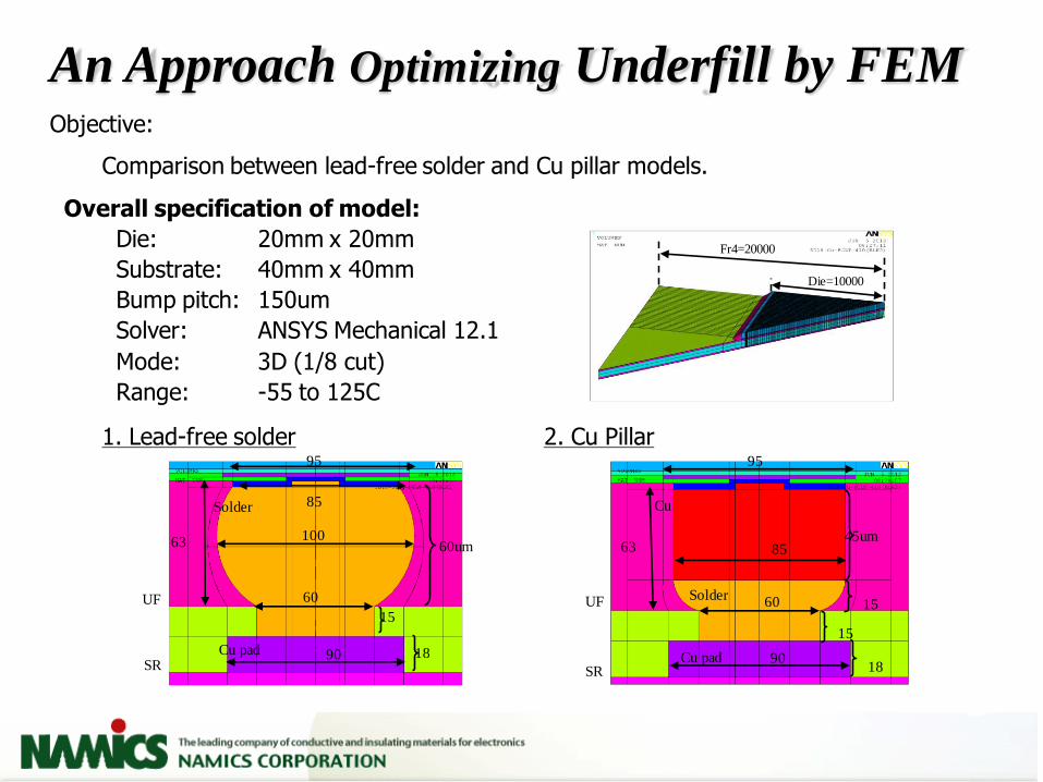
Objective:
Comparison between lead-free solder and Cu pillar models.
Die=10000
Fr4=20000
Overall specification of model:
Die: 20mm x 20mm
Substrate: 40mm x 40mm
Bump pitch: 150um
Solver: ANSYS Mechanical 12.1
Mode: 3D (1/8 cut)
Range: -55 to 125C
1. Lead-free solder 2. Cu Pillar
Cu pad
Solder
Cu
1890
60
15
15
45um85
95
UF
SR
63
60
Solder 85
100
95
60um
UF
SRCu pad
63
18
15
90
An Approach Optimizing Underfill by FEM

1. Lead-free solder 2. Cu Pillar
X-sectional schematics
High strain points shown for Lead Free & Cu Pillar. Tg is strongly correlated to creep strain of solder in both structure. A high Tg underfill is required for bump protection.
0
0.1
0.2
0.3
0.4
7000M
Pa
10000M
Pa
13000M
pa
30M
Pa
180M
Pa
330M
Pa
80C
120C
160C
20ppm
/C28ppm
/C36ppm
/C
70ppm
/C100ppm
/C130ppm
/CE1 E2 Tg CTE1 CTE2
Str
ain
(-)
Lead-free solder
Cu pillar
Solder Creep Strain

1. Lead-free solder 2. Cu Pillar
X-sectional schematics
Note the significant difference of low-K stress between lead-free solder to Cu pillar. In case of Cu pillar, high Tg is slightly better. Overall there is limited impact on Low-K when looking at Tg.
0
50
100
150
200
250
300
7000M
Pa
10000M
Pa
13000M
pa
30M
Pa
180M
Pa
330M
Pa
80C
120C
160C
20ppm
/C28ppm
/C36ppm
/C
70ppm
/C100ppm
/C130ppm
/CE1 E2 Tg CTE1 CTE2
Str
ess(M
Pa)
Lead-free solder
Cu pillar
Low-K Dielectric Stress

In both cases, lower Tg will provide lower warpage.
Hig
h
L
ow
-360
-340
-320
-3007000M
Pa
10000M
Pa
13000M
pa
30M
Pa
180M
Pa
330M
Pa
80C
120C
160C
20ppm
/C28ppm
/C36ppm
/C
70ppm
/C100ppm
/C130ppm
/CE1 E2 Tg CTE1 CTE2
Warp
age(u
m)
Lead-free solder
Cu pillar
Package Warpage

- Cu Pillar & Lead free bumps require a higher Tg to offer excellent protection from bump fracture during TCT.
- However low Tg may can assist with warpage, delamination and failure.
Modeling Summary
Bump Protection
Warpage
Underfill for FC-BGA/FC-CSP for Cu Pillar
# An approach optimizing Underfill property by modeling
# Avoiding Filler separation
# Void elimination for narrow gap
Underfill Challenges and Solutions

‘Filler separation’ is NOT a phenomenon of ‘more
settled down’, should be occurred by another factor
Cause: Gravitation forceCause: Unknown
Has no filler Fine particles
are remaining
Filler separation Filler settling
Confirmation of Filler Separation vs Filler Setting

Eutectic
solder (Sn/Pb)
Cu
Delamination by sample preparation
Separation is specifically on Cu-Sn interface.
V
2 different metal
2 different metal
electrolysis solution
Voltaic Battery
Element E0(V)
Li -3.045
K -2.925
Ca -2.840
Na -2.714
Mg -2.356
Al -1.676
This phenomenon means
Cu becomes positive(+) and Sn becomes
negative(-) electrode by the difference between
their Standard Electrode Potential (table right)
We think that Cu and Eutectic
solder works as a battery
And the voltage separates filler
and resin
Cu
0.340V
Sn
-0.138V
+
-
Standard Electrode Potential
Element E0(V)
Zn -0.763
Fe -0.440
Ni -0.257
Sn -0.138
Pb -0.126
H 0.000
Element E0(V)
Cu 0.340
Hg 0.796
Ag 0.799
Pt 1.188
Au 1.520
0.478V

1. Electrostatic charge of particle (Filler) 2. Electrophoretic effect
Filler
+
-- - -
----
-
+ + + ++
+
+
+
+
+
+
++
+ + +
---
- - -
SiO2 filler is Electrostatic charged and it
can be kept dispersed by the repulsive
force of charged ion
++
-+
-
-+
-+
+
+
+
+
+
+
+
Resin +
+
+
+
+
+
+
+
+
+
-
-
-
-
-
+
+
+++
++
+
+
+++
++
+
+
+++
++
+
+
+++
++
+
+
+++
++
+
+
+++
++
+
+
+++
++
+
+
+++
++
+
+
+++
++
+
+
+++
++
-
-
-
-
-
-
-
-
-
-
-
-
-
+
+
+++
++
-
-
-
-
-
Filler is migrated with the charged ion
together while voltage occurred
Ion charge
Electrostatic
charge
Our hypothesis
Why the voltage makes separation?

Test specimen
InitialCu wire (plated Sn)
L/S=25/25um
Electrode
Polyimide base film
Diagram
Procedure
After curedUnderfill
1. Put underfill onto the Cu wire
2. Put the specimen into oven (165C)
3. Turn on the switch(SW) to apply voltage
between 2 electrodes
4. Cure the specimen (2h)
5. Turn off the switch(SW)
6. Cut the specimen and the cross section
view is observed
SW
Underfill
Cross-section line
Electrode
Confirmation Test

(+)(-)
Filler separation like occurred in Cu-pillar PKG is confirmed by applying voltage.
(+)(-)
- No
applied
voltage
- Applied
+5VDC
Testing Results

The phenomenon
is influenced to
voltage.
- Not applied voltage
- Applied +5VDC
- Applied +1VDC
(+)(-)
(+)(-)
Step 1; Influence of Voltage
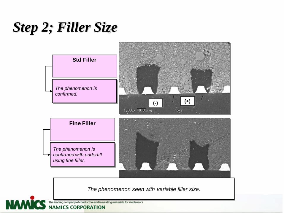
Step 2; Filler Size
Std Filler
Fine Filler
(+)(-)
The phenomenon is
confirmed with underfill
using fine filler.
The phenomenon is
confirmed.
The phenomenon seen with variable filler size.

Step 3; Curing System
Different curing system
to previous material.
Faster Gel time!
The phenomenon is
improved with underfill has
different curing system
Faster gel time does offer some assistance, but phenomena is still seen.

The phenomenon is
confirmed and
almost same to
165C curing
165C/2h
(+)(-)
The phenomenon is
confirmed.
175C/2h
(+)(-)
The phenomenon is not changed by underfill curing condition
Step 4; Curing Conditions

Condition Filler separation
1. Voltage Accelerated by voltage increasing
2. Underfill with fine filler Not improved
3. Underfill with different curing system Improved
4. Underfill curing condition Not improved
Filler separation is occurred by voltage and it is changed
by underfill curing system.
Summary

(+)(-)(+)(-)
Not applied voltage Applied +5VDCInfluence of voltage
1. Our opinion is the filler separating phenomenon has been occurred by the migration of filler by voltage
Battery effect of 2 different metals
2. And the voltage is related to the bump material
Eutectic solder
(Sn/Pb)
Cu
There are a possibility that it
happens on other bump structures.
In some cases of the differential of
alignment of die and substrate will
make metals working as a battery.
Conclusion
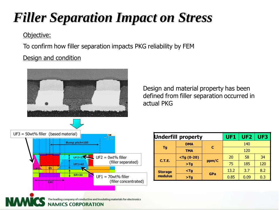
Bump pitch=150
SR=33
UF3=42
UF2=21
130 92.206
137.206
85UF1
Bump pitch=150
SR=33
UF1=42
UF2=21
130
85UF3
Bump pitch=150
SR=33
UF3=42
UF2=21
130 92.206
137.206
85UF1
Bump pitch=150
SR=33
UF1=42
UF2=21
130
85UF3
Underfill property UF1 UF2 UF3
TgDMA
C140
TMA 120
C.T.E. <Tg (0-20)
ppm/C20 58 34
>Tg 75 185 120
Storage modulus
<TgGPa
13.2 3.7 8.2
>Tg 0.85 0.09 0.3
UF2 = 0wt% filler(filler separated)
UF1 = 70wt% filler(filler concentrated)
UF3 = 50wt% filler (based material)
Objective:
To confirm how filler separation impacts PKG reliability by FEM
Design and condition
Design and material property has been defined from filler separation occurred in actual PKG
Filler Separation Impact on Stress

Low-K stress
0
50
100
150
200
250
300
Without filler separation With filler separation
Low
-K s
tres
s (M
Pa)
+7.7%
Stress on Low-K was increased by filler separation
FEM Low-K Dielectric Stress w/ Filler Separation

Underfill stress
0
50
100
150
200
250
300
350
400
Without filler separation With filler separation
Un
der
fill
stre
ss (
MP
a)
A: Fillet top B: Die corner C: Around the bump
A: no changeB: no changeC: +22%
A: Fillet top
B: Die corner
C: Around the bump
A,B C A,B C
Underfill stress around the bump increased due to filler separation
FEM Underfill Stress w/ Filler Separation

Underfill for FC-BGA/FC-CSP for Cu Pillar
# An approach optimizing Underfill property by modeling
# Avoiding Filler separation
# Void elimination for narrow gap
Underfill Challenges and Solutions

Filler cohesion during underfill flow reduces flow velocity in locations, this phenomena will cause flow marks and capture voids.
Flo
w d
irection
Flowmark
FastSlow
Captured void
Cross-sectional schematics
Uniform flow= Flows fast
Filler cohesion / stuck= Flows slow
Flow direction Flow direction
Mechanism of Flowmarks

Applying proprietary treatment to filler prevented the filler from cohesion.
Conventional UnderfillMany flow marks and voids
Improved w/ filler treatmentNo flow mark
Flow mark
Test specimen for flowability
Gap:10um
Underfill
Glass
Glass
10mm
20mm
Hot plate
Captured void
Improvement of Voids caused by Flowmarks
Vacuum assisted process Curing process with Pressure oven
Equipment Vacuum system Pressure oven
Void reduction process At underfilling At curing
A sort of void to eliminate Capture Capture, Moisture
Size of void to eliminate Large ~ Small Small
Underfill VCUF CUF
Dispensing Underfilling Curing Completion
Vacuum assisted process
Void elimination
Curing process with Pressure oven
Void elimination
Void Elimination Process

Under a vacuum condition
Round shape dispensing
DispenseComplete
Underfilling
Flow by Capillary action
and differential pressureNo void
Gap: 20um
Demonstration 1
Tem
pera
ture
Pre
ssu
re
Time20sec 20sec
About About
Set onto heated stage in
vacuum chamber
(130Pa, 70 – 110C)Penetration process
Accelerates with positive pressure
negative
pressure
positive
pressure
C-SAM View
IBM test vehicle
19 x 19mm die
150um pitch, Pb free C4Ref. Horibe, ECTC2011
Microscope View
Vent
Under atmospheric pressure
Vacuum Assisted Processing

Before cure
After cure
UFPressure-oven
TypePressure value
NAMICS VFS-60A-JP 7 kg/cm2
Capture void investigation
Voids disappear.
Capture void
Voids remain.
Pressure oven profile
2030405060708090
100110120130140150160170180
0 15 30 45 60 75 90 105 120 135 150 165 180
Time (min.)
Tem
pera
ture
(d
eg
.C)
1
2
3
4
5
6
7
8
9
10
Pre
ssu
re (
Kg
/cm
2)
Temperature Pressure
Pressure-ovenOven
TEST vehicleDie size : 20mmx20mmx0.73mm(t)Passivation : PIBump material : Sn/3Ag/0.5CuBump pitch : 175umFlux : non-cleanSubstrate size : 52.5mmx30.0mmx0.73mm(t)
Void Investigation w/Pressure-oven

FEM helps us to tailor underfill materials to the package needs.
Needs vary from package to package design.
Avoid filler separation as it can lead to increases in stress concentration
CUF provides narrow gap penetration and high jet dispense stability, also
new function with high thermal conductivity, vacuum assist process.
Summary