
2005 IBM Power and Cooling Technology Symposium ... · 2005 IBM Power and Cooling Technology...
21
2005 IBM Power and Cooling Technology Symposium Advancements in Power Interconnect Presenter: Don Wood Date: September 21, 2005
Transcript of 2005 IBM Power and Cooling Technology Symposium ... · 2005 IBM Power and Cooling Technology...

October 7, 2005
1
2005 IBM Power and Cooling Technology Symposium
Advancements in Power Interconnect
Presenter: Don Wood
Date: September 21, 2005
October 7, 2005
2
October 7, 20052
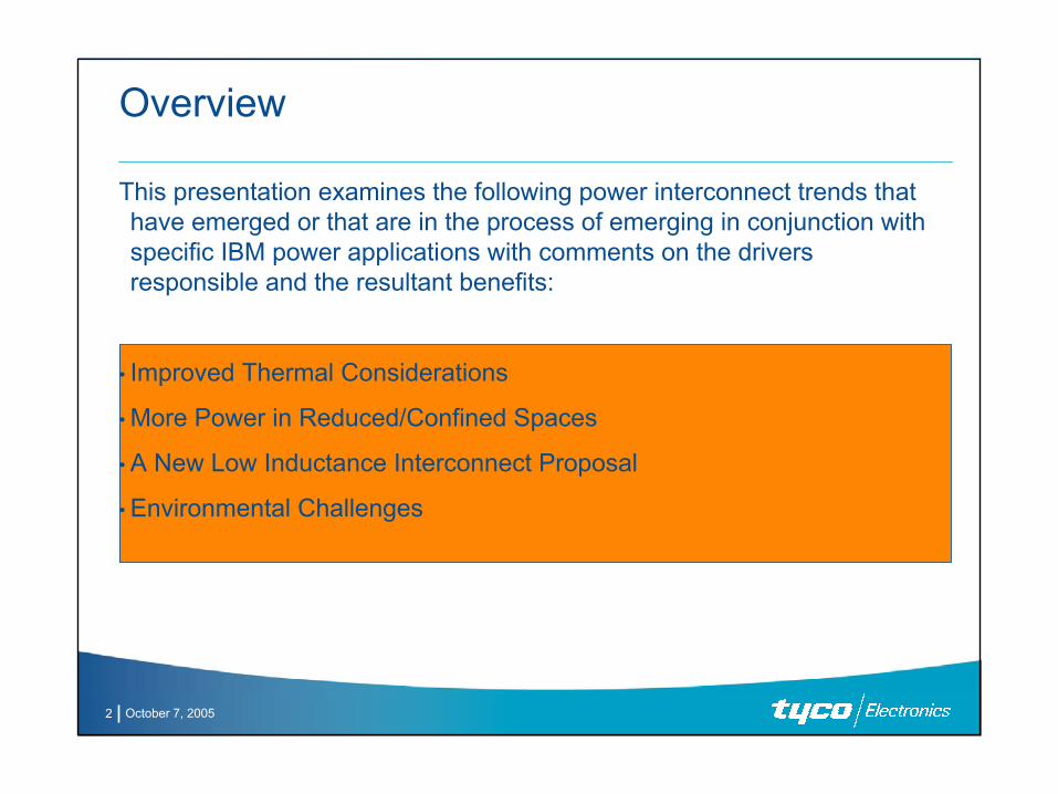
Overview
This presentation examines the following power interconnect trends that have emerged or that are in the process of emerging in conjunction with specific IBM power applications with comments on the drivers responsible and the resultant benefits:
• Improved Thermal Considerations
• More Power in Reduced/Confined Spaces
• A New Low Inductance Interconnect Proposal
• Environmental Challenges

October 7, 2005
3
October 7, 20053
Improved Thermal Considerations – Airflow Impedance• Packaging shift to coplanar power card to system board orientation
• Connector profile off the board surface is having an increasingly important impact on the airflow particularly in systems where the power supply cooling is an integral part of the system thermal management
• Alternate connector construction can reduce the impedance effect by utilizing a coplanar mating scheme with a net height reduction of 66% vs conventional power connectors or 50% vs a right angle card edge style connector
October 7, 2005
4
October 7, 20054
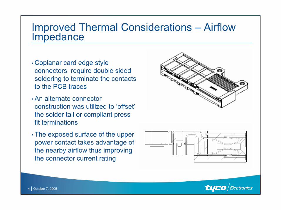
Improved Thermal Considerations – Airflow Impedance
• Coplanar card edge style connectors require double sided soldering to terminate the contacts to the PCB traces
• An alternate connector construction was utilized to ‘offset’ the solder tail or compliant press fit terminations
• The exposed surface of the upper power contact takes advantage of the nearby airflow thus improving the connector current rating
October 7, 2005
5
October 7, 20055
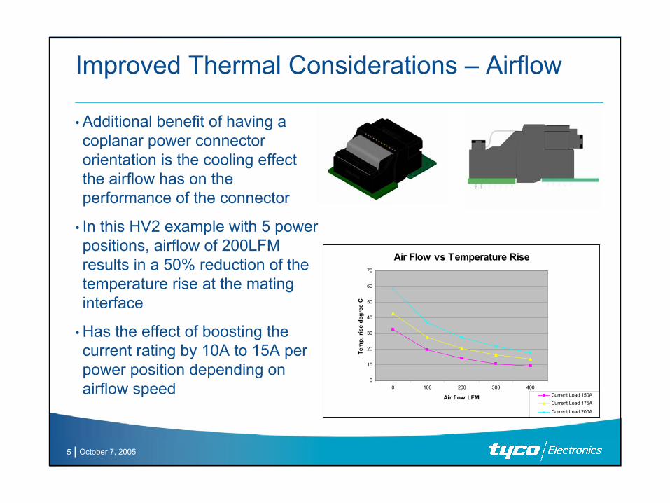
Improved Thermal Considerations – Airflow
• Additional benefit of having a coplanar power connector orientation is the cooling effect the airflow has on the performance of the connector
• In this HV2 example with 5 power positions, airflow of 200LFM results in a 50% reduction of the temperature rise at the mating interface
• Has the effect of boosting the current rating by 10A to 15A per power position depending on airflow speed
Air Flow vs Temperature Rise
0
10
20
30
40
50
60
70
0 100 200 300 400
Air flow LFM
Tem
p. ri
se d
egre
e C
Current Load 150ACurrent Load 175A
Current Load 200A
October 7, 2005
6
October 7, 20056
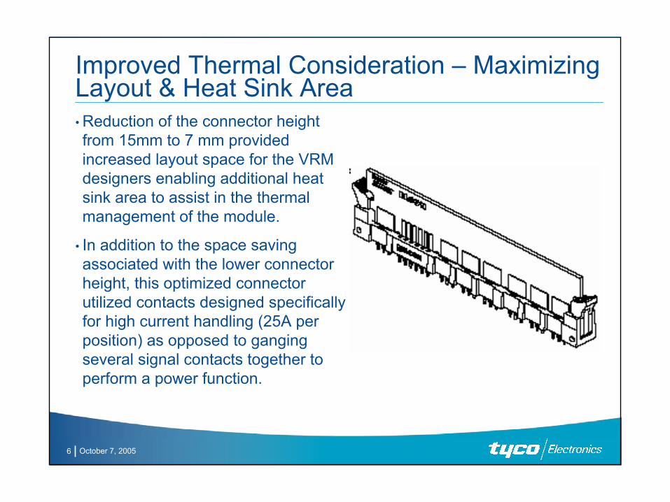
Improved Thermal Consideration – Maximizing Layout & Heat Sink Area• Reduction of the connector height from 15mm to 7 mm provided increased layout space for the VRM designers enabling additional heat sink area to assist in the thermal management of the module.
• In addition to the space saving associated with the lower connector height, this optimized connector utilized contacts designed specifically for high current handling (25A per position) as opposed to ganging several signal contacts together to perform a power function.
October 7, 2005
7
October 7, 20057
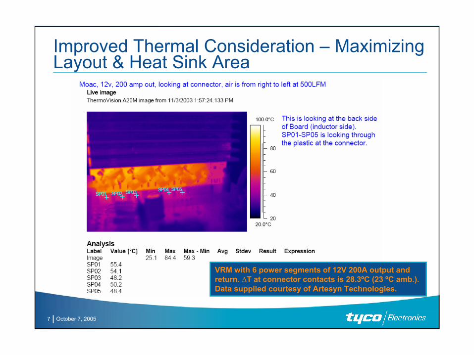
Improved Thermal Consideration – Maximizing Layout & Heat Sink Area
VRM with 6 power segments of 12V 200A output and return. ∆T at connector contacts is 28.3ºC (23 ºC amb.). Data supplied courtesy of Artesyn Technologies.

October 7, 2005
8
October 7, 20058
Improved Thermal Consideration – Maximizing Layout & Heat Sink Area
VRM with 6 power segments of 12V 240A output and return. ∆T at connector contacts is 38.5ºC (23 ºC amb.). Data supplied courtesy of Artesyn Technologies.
October 7, 2005
9
October 7, 20059
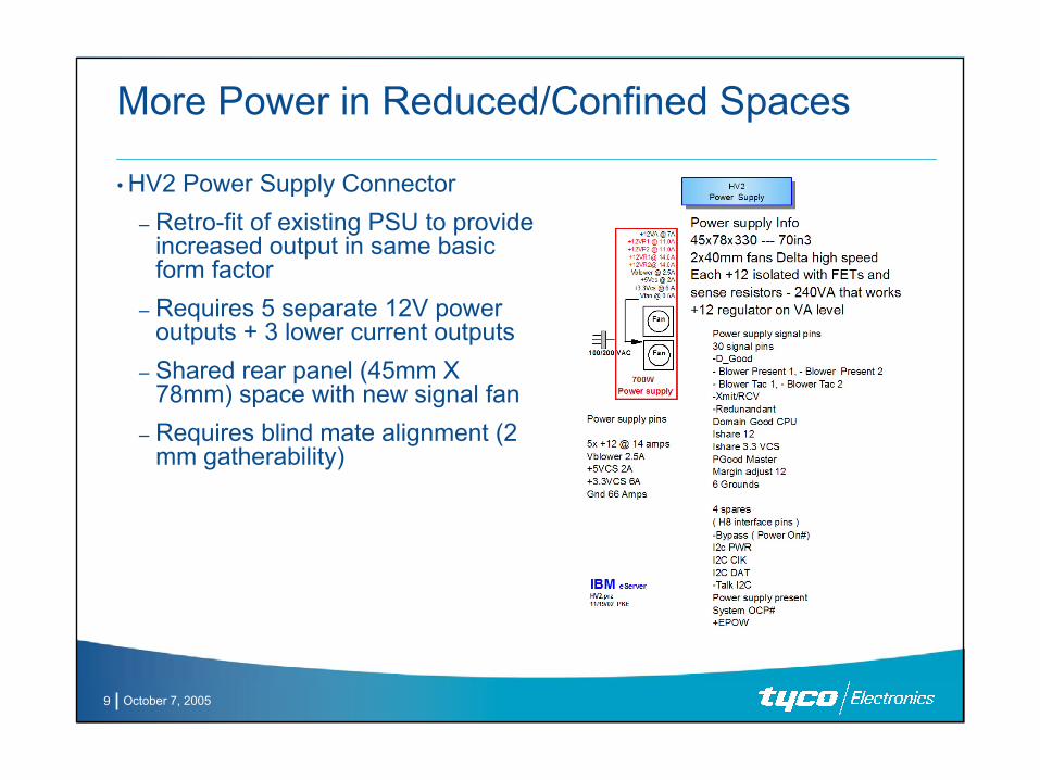
More Power in Reduced/Confined Spaces
• HV2 Power Supply Connector– Retro-fit of existing PSU to provide
increased output in same basic form factor
– Requires 5 separate 12V power outputs + 3 lower current outputs
– Shared rear panel (45mm X 78mm) space with new signal fan
– Requires blind mate alignment (2 mm gatherability)
October 7, 2005
10
October 7, 200510
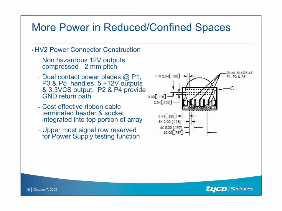
More Power in Reduced/Confined Spaces
• HV2 Power Connector Construction– Non hazardous 12V outputs
compressed - 2 mm pitch– Dual contact power blades @ P1,
P3 & P5 handles 5 +12V outputs & 3.3VCS output. P2 & P4 provide GND return path
– Cost effective ribbon cable terminated header & socket integrated into top portion of array
– Upper most signal row reserved for Power Supply testing function

October 7, 2005
11
October 7, 200511
More Power in Reduced/Confined Spaces
• Integrated AC Input & DC Output– Applications with limited connector
access area may consider this design alternative
– AC input voltage is wired as a feed-thru termination – keeping AC lines of system board and allowing discrete internal PSU routing
– DC output and signal contacts are handled in conventional PCB to PCB power connector configurations
October 7, 2005
12
October 7, 200512
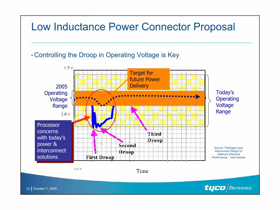
Low Inductance Power Connector Proposal
• Controlling the Droop in Operating Voltage is Key
Source: “Package-Level Interconnect Design for
Optimum Electrical Performance,” Intel website
2005Operating
VoltageRange
Processorconcernswith today’spower &interconnectsolutions
Processorconcernswith today’spower &interconnectsolutions
Target for future Power Delivery
Today’sOperatingVoltageRange
October 7, 2005
13
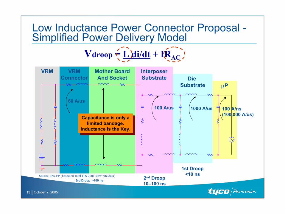
October 7, 200513
Low Inductance Power Connector Proposal -Simplified Power Delivery Model
VRMConnector
3rd Droop >100 ns
Mother BoardAnd Socket
InterposerSubstrate Die
Substrate µP
VRM
1st Droop<10 ns
2nd Droop10–100 ns
60 A/us100 A/us 1000 A/us 100 A/ns
(100,000 A/us)
Source: INCEP (based on Intel ITS 2001 slew rate data)
Capacitance is only a limited bandage.
Inductance is the Key.
Capacitance is only a limited bandage.
Inductance is the Key.
Vdroop = L di/dt + IRAC
October 7, 2005
14
October 7, 200514
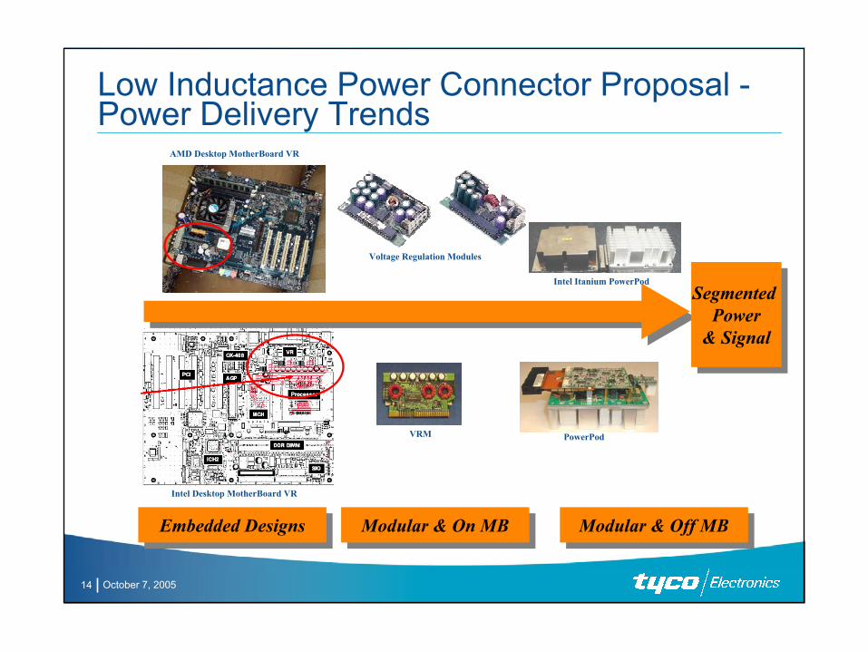
Low Inductance Power Connector Proposal -Power Delivery Trends
Embedded DesignsEmbedded Designs Modular & On MBModular & On MB Modular & Off MBModular & Off MB
Intel Itanium PowerPod
PowerPod
Voltage Regulation Modules
Intel Desktop MotherBoard VR
AMD Desktop MotherBoard VR
VRM
Segmented Power
& Signal
Segmented Power
& Signal

October 7, 2005
15
October 7, 200515
Processor boardPower connectors
Heat spreader
Power board
Memory ASIC
Microprocessors
Power interconnection devices between Power interconnection devices between VRMVRM and and CPU/ASICCPU/ASIC planes with optimized topologyplanes with optimized topology
Characterization of High Performance, Low Inductance Power Connector

October 7, 2005
16
October 7, 200516
The Card Edge Power Connector Approach
Very high power density Very high power density (more than 100A/inch(more than 100A/inch22))Loop inductance of 1 nHLoop inductance of 1 nHLow profile for optimized Low profile for optimized component placingcomponent placing

October 7, 2005
17
October 7, 200517
Low Inductance Power Connector Proposal –Using Inter-digitated Planes
To achieve lowest resistance possible...To achieve lowest resistance possible...Small gap between power and returnSmall gap between power and returnShort path lengthShort path lengthHigh crossHigh cross--section areasection area
As the gap between power and return paths decreases,As the gap between power and return paths decreases,the electromagnetic coupling increases enabling the the electromagnetic coupling increases enabling the magnetic field cancellation to become effective, and magnetic field cancellation to become effective, and
lower the loop inductance.lower the loop inductance.

October 7, 2005
18
October 7, 200518
Low Inductance Power Connector Proposal
Lower inductance Lower inductance –– 130 pH range130 pH rangeBetter utilization of PCB real estateBetter utilization of PCB real estateLow profile to achieve short path Low profile to achieve short path length & lower resistancelength & lower resistanceMore contact fingers reduce loop More contact fingers reduce loop inductanceinductance
Contact fingerContact finger
InIn--line planesline planesin very closein very closeproximityproximity

October 7, 2005
19
October 7, 200519
Environmental Challenges
Tyco Electronics is an industry leader in developing RoHS/Lead-free solutions and is well positioned to support our customer’s conversion to
RoHS complianceTE has and continues to conduct product/process testing to ensure
adequate product performance in lead free environmentOur policy has been to share information with customers and industry as appropriate (reference the technical information available on our
website –links on following page)Actively participates in industry consortia focused on lead free/RoHS
activitiesMonitoring status and providing stakeholder input as appropriate to
affect additional RoHS exemptions under consideration by European Commission
• Tyco Electronics is an industry leader in developing RoHS Compliant solutions and is well positioned to support our customer’s conversion to RoHS compliance.
• Tyco Electronics has and continues to conduct product/process testing to ensure adequate product performance in a lead free environment.
• Power connectors have had to deal with a much less obvious issuerelated to hexavalent chromium (Cr6+) content:
– The larger current carrying style contacts used in the panel mount power cable harnesses utilize a silver plated finish to ensure reliable robust connection.
– The tarnish inhibitor applied to the silver plated surfaces with the most common tarnish inhibitors containing the hexavalent chromium.
– Recent internal evaluations have identified an alternative which has been tested and proven to meet Tyco Electronics specification requirements.

October 7, 2005
20
October 7, 200520
Environmental Challenges
Tyco Electronics is an industry leader in developing RoHS/Lead-free solutions and is well positioned to support our customer’s conversion to
RoHS complianceTE has and continues to conduct product/process testing to ensure
adequate product performance in lead free environmentOur policy has been to share information with customers and industry as appropriate (reference the technical information available on our
website –links on following page)Actively participates in industry consortia focused on lead free/RoHS
activitiesMonitoring status and providing stakeholder input as appropriate to
affect additional RoHS exemptions under consideration by European Commission
Internal Tarnish Inhibitor Analysis; Replacement of Hexavalent Chromium
UntestedUntestedUntestedUntestedUntestedUntestedFailedAlternative E
UntestedUntestedUntestedUntestedUntestedUntestedFailedAlternative D
PassPassPassPassPassFailedPassAlternative C
PassPassPassPassPassFailedPassAlternative B
PassPassPassPassPassPassPassAlternative A
PassPassPassPassPassPassPassChromate
SolderabilityContact Resistance
Durability (insertion/ extraction cycling)
Insertion/ extraction
Force
Solder TestAmmonium Sulfide Test after 8 hours @140 deg. F
Ammonium Sulfide Test
Post Plating Treatment Tested
October 7, 2005
21
October 7, 200521
Conclusion
Recent advancements in the power interconnect area have fostered increased power circuit density, higher current ratings and resolution of constrained space limitations. The collaborative dialogue that exists within the IBM design community is a key element in driving these advancements and achieving improved performance objectives. Tyco Electronics looks forward to continuing this role and providing future advancements to keep pace with IBM’s needs.
Tyco is a trademark. Other products, logos, and Company names mentioned herein may be trademarks of their respective owners.


