Geochemical Characteristics and Modeling of Conventional ...

i
2-D MODELING OF SUBTHRESHOLD
CHARACTERISTICS OF SYMMETRIC
AND ASYMMETRIC DOUBLE GATE
JUNCTIONLESS FIELD EFFECT
TRANSISTORS
A thesis submitted in partial fulfillment of the requirements for the degree of
Master of Science in Electrical and Electronic Engineering
by
Imtiaz Ahmed Student No: 0412062214 P
Department of Electrical and Electronic Engineering
Bangladesh University of Engineering and Technology August, 2015

ii
Approval The thesis titled “2-D MODELING OF SUBTHRESHOLD CHARACTERISTICS OF SYMMETRIC AND ASYMMETRIC DOUBLE GATE JUNCTIONLESS FIELD EFFECT TRANSISTORS” submitted by Imtiaz Ahmed, Student No: 0412062214 P, Session: April 2012, has been accepted as satisfactory in partial fulfillment of the requirements for the degree of Master of Science in Electrical and Electronic Engineering on August 31, 2015.
Board of Examiners
1. _____________________________________________________ Dr. Quazi Deen Mohd Khosru Chairman Professor (Supervisor) Department of Electrical and Electronic Engineering Bangladesh University of Engineering and Technology Dhaka – 1205, Bangladesh. 2. _____________________________________________________ Dr. Satya Prasad Majumder Member Professor and Head (Ex-officio) Department of Electrical and Electronic Engineering Bangladesh University of Engineering and Technology Dhaka – 1205, Bangladesh. 3. _____________________________________________________ Dr. Md. Shafiqul Islam Member Professor Department of Electrical and Electronic Engineering Bangladesh University of Engineering and Technology Dhaka – 1205, Bangladesh. 4. _____________________________________________________ Dr. Zahid Hasan Mahmood Member Professor (External) Department of Electrical and Electronic Engineering University of Dhaka Dhaka-1000, Bangladesh.

iii
Declaration It is hereby declared that this thesis or any part of it has not been submitted elsewhere for the award of any degree or diploma. Signature of the Candidate ____________________________________ (Imtiaz Ahmed)

iv
To my beloved parents

v
Acknowledgment
First of all, I would like to thank Almighty for giving me strength and patience to complete this thesis.
I would then like to express my sincere gratitude to my thesis supervisor Dr. Quazi Deen Mohd Khosru, Professor, Department of Electrical and Electronic Engineering (EEE), Bangladesh University of Engineering and Technology (BUET), for his generous help, encouragement and support throughout the entire thesis work. Whenever I faced problems and didn’t know how to proceed, he pointed me to the right direction. I am also grateful to him for offering me the perfect balance of freedom and guidance. His passion for research will always be an inspiration to me.
I am also thankful to the Head of EEE Department, Dr. Taifur Ahmed Chowdhury for his support during my thesis work. I would also like to thank the members of the board of examiners for taking the time to evaluate my work and provide necessary suggestions.
I want to express my gratitude to Mr. Nadim Chowdhury, Assistant Professor, Department of Electrical and Electronic Engineering (EEE), Bangladesh University of Engineering and Technology (BUET), for his kind and sincere helps and discussions in solving various numerical problems related to the thesis work.
I would like to thank my parents, M. Momtaz Uddin and Rozyna Parvin. I also want to dedicate my thesis to them. They have helped me in every possible way throughout this journey. This thesis work would not have been possible without their help.
Finally, I owe my sincere gratitude to all who were directly or indirectly related to this work for their support and encouragement.

vi
Abstract
The miniaturization of traditional planar Metal Oxide Semiconductor Field Effect Transistors (MOSFETs) becomes quite challenging for very short channel devices as the formation of ultra-sharp source and drain junctions with a high process complexity is needed. Junctionless Field Effect Transistors (JLFETs) are considered promising for the sub-20 nm era due to their constant doping profile from source to drain. They provide a great scalability without the need for rigorously controlled doping and activation techniques as well as reduced short channel effects (SCEs) compared to the conventional MOSFETs. Though a number of analytical and simulation studies based on one-dimensional (1-D) model for Double Gate (DG) JLFETs have been carried out over the past few years but rigorous and accurate two-dimensional (2-D) analytical study on this device is yet to be reported. This work proposes a physically based analytical model of 2-D electrostatic potential in the channel applicable for both symmetric and asymmetric DG JLFETs considering similar and dissimilar gate biased configurations operating in the subthreshold region. The model is derived by solving 2-D Poisson’s equation along the channel while assuming a cubic potential distribution across the silicon thickness using appropriate boundary conditions and 1-D capacitance model. Different device parameters like channel doping concentration, thicknesses of silicon channel, top and bottom gate oxide, gate length, applied drain and gate biases, flat-band voltages of gates etc. are included in this model. To justify the accuracy of the model, Poisson’s equation with the same boundary conditions is solved in the COMSOL Multiphysics using Finite Element Method (FEM) and the obtained results are matched with those of the modeled ones. The obtained results from analytical model is also matched with SILVACO ATLAS simulation results to underpin the validity of this model. The proposed potential model is compared with the reported data available in the literature for short channel symmetric DG JLFET. In order to avoid extensive mathematical complexity numerical techniques by MATLAB is further used to calculate threshold voltage, subthreshold drain current and different SCEs viz. threshold voltage roll-off (TVRO), drain induced barrier lowering (DIBL), subthreshold swing (SS) from the proposed analytical model for different structures of DG JLFETs. A detail comparative study of potential distribution in the channel region for different gate and drain voltages obtained from the proposed analytical model is performed for symmetric and asymmetric DG JLFETs. The effect of bottom gate flat-band voltage of asymmetric structures and bottom gate voltage of dissimilar gate biased structures on the threshold voltage are investigated. Finally a performance comparison of subthreshold behavior i.e. TVRO, DIBL, drain current and SS have been made between symmetric and asymmetric DG JLFETs. Both symmetric and asymmetric DG JLFETs show nearly ideal TVRO (~0V), DIBL (~0mV/V) and SS (~60mV/decade) at the gate length around 50nm which make them good competitors of the conventional MOSFETs for short channel devices.

vii
Contents Page Approval ii Declaration iii Acknowledgement v Abstract vi Contents vii List of Figures x List of Tables xiv List of Abbreviations xv List of Symbols xvi 1. Introduction 1
1.1. Current Trend of CMOS Technology and Future Roadmap 1 1.1.1. CMOS Scaling and Challenges Owing to Short Channel Effects 1
1.1.1.1.Hot Carrier Effects 3 1.1.1.2.Gate Oxide Leakage 3 1.1.1.3.Channel Length Modulation 4 1.1.1.4.Drain Induced Barrier Lowering 4 1.1.1.5.Subthreshold Swing 5
1.1.2. Various Approaches for the Continuation of Moore’s Law 5 1.2. Junctionless Field Effect Transistors 8
1.2.1. Theory of Junctionless Field Effect Transistors 8 1.2.2. State-of-the-Art-Junctionless Field Effect Transistors 10
1.2.2.1.Models 10 1.2.2.2.Technologies 13
1.3. Thesis Objectives 14 1.4. Thesis Organization
15

viii
2. Analytical Model Development 16 2.1. Device Structure 16 2.2. Electrostatic Potential Modeling 17
2.2.1. Poisson Equation 17 2.2.2. Cubic Approximation 17 2.2.3. Boundary Conditions 17 2.2.4. Coefficients Determination 18 2.2.5. Capacitance Model 19 2.2.6. Channel Potential 21
2.3. Threshold Voltage and DIBL Calculation 24 2.4. Drain Current and Subthreshold Swing Calculation 25
3. Simulation Model Development 26
3.1. SILVACO ATLAS 26 3.1.1. ATLAS Commands 27 3.1.2. Structure and Model Development 28
3.1.2.1.Mesh 28 3.1.2.2.Region 29 3.1.2.3.Electrode 30 3.1.2.4.Doping 31 3.1.2.5.Contact 32 3.1.2.6.Model 32
3.1.3. Numerical Method Selection 33 3.1.4. Output Specification 33 3.1.5. Solution Specification 34 3.1.6. Results 34
3.2. COMSOL Multiphysics 37 3.2.1. Model Development in COMSOL Multiphysics 3.5 37
3.2.1.1.Model Navigator 37 3.2.1.2.Geometry Modeling 38 3.2.1.3.Physics Modeling 40 3.2.1.4.Mesh generation and Computing Solution 41 3.2.1.5.Saving Model 42
4. Results and Discussions 44
4.1. Model Verification 44 4.2. Performance Comparison 52
4.2.1. Channel Potential Distribution 54

ix
4.2.2. Threshold Voltage 63 4.2.3. Short Channel Effects 65
5. Conclusion 70
5.1. Summary 70 5.2. Suggestions for Future Work 71
Bibliography 72

x
List of Figures
Page
1.1 Scaling trend of high performance logic technologies with year [1]. 1
1.2 Punch-through effect in a short channel MOSFET [3]. 2
1.3 Schematic illustration of hot carrier effects in MOSFETs. 3
1.4 Schematic illustration of channel length modulation effect. 4
1.5 (a) Retrograde channel doping profile gives a high performance in a MOSFET. (b) The lattice mismatch between SiGe and Si can improve the mobility of MOSFET [2]. 5
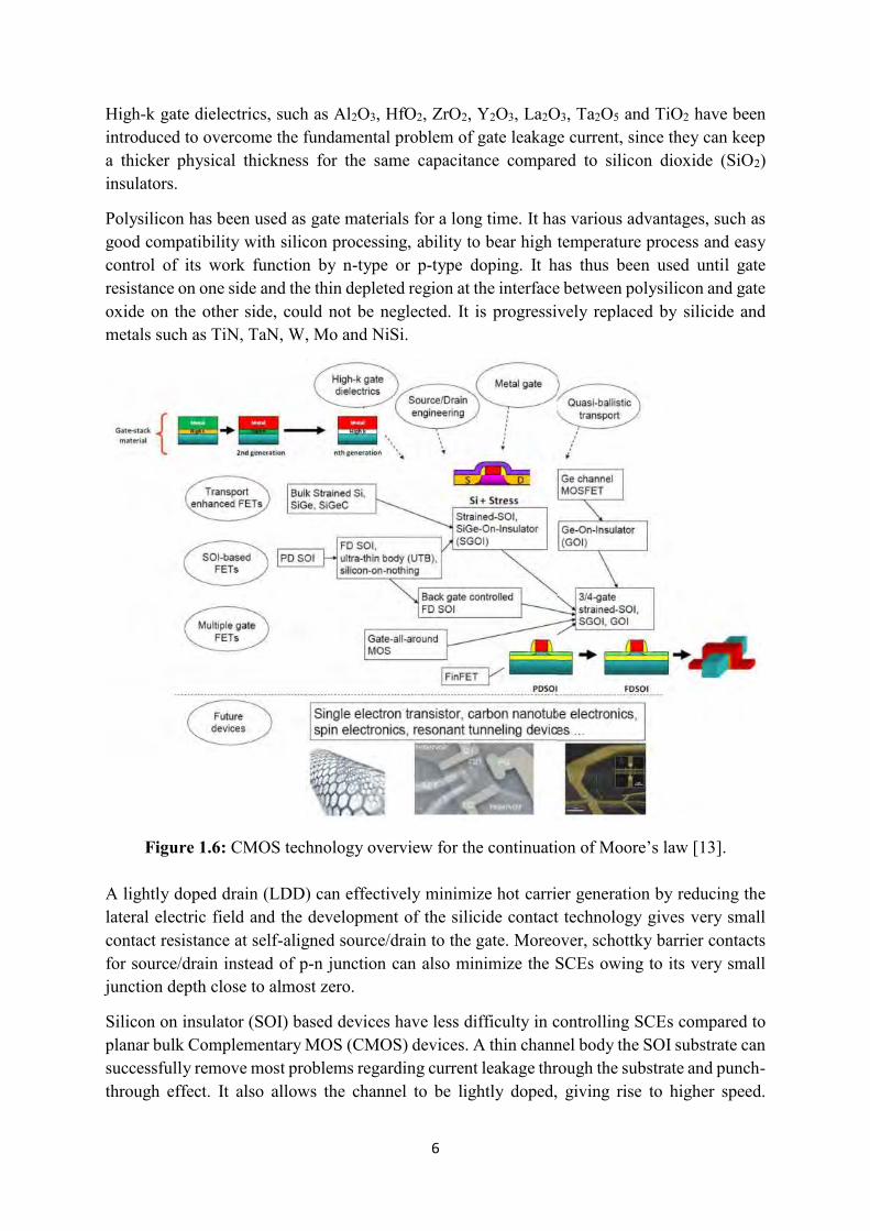
1.6 CMOS technology overview for the continuation of Moore’s law [13]. 6
1.7 Schematic of hybrid crossbar/CMOS circuits made of bottom-up based nanowires materials [9]. 7
1.8 Illustration of different JLFET structures, (a) single gate silicon on insulator (SG SOI) and (b) double gate (DG) structure. 8
1.9 (a) Depletion, (b) bulk current, (c) flat-band and (d) accumulation mode of DG JLFET. The source/drain regions are not shown to simplify matters. 9
1.10 Band diagram from gate to gate of the DG JLFET. The device operates in: (a) depletion, (b) flat-band and (c) accumulation mode. 9
1.11 Drain current variation with gate voltage for (a) IM MOSFETs and (b) JLFETs [19]. 10
2.1 Schematic cross-sectional view of a DG JLFET. 16
2.2 (a) Two terminal structure and (b) 1-D capacitance model of DG JLFET in the subthreshold region. 20
3.1 ATLAS inputs and outputs [62]. 27
3.2 Mesh creation for DG JLFET. 29
3.3 Different regions of DG JLFET. 30

xi
3.4 Different electrodes of DG JLFET. 31
3.5 Net doping in different regions of DG JLFET. 32
3.6 2-D structure of DG JLFET developed in SILVACO ATLAS. 35
3.7 Potential of symmetric DG JLFET along top to bottom gate direction for
dsV = 0.1V and gsV = 0V considering gL = 50nm, sit = 10nm, 1oxt =
2oxt
= 1.5nm and dN = 1019cm-3. 35
3.8 Potential of symmetric DG JLFET along source to drain direction for
dsV = 0.1V and gsV = 0V considering gL = 50nm, sit = 10nm, 1oxt =
2oxt
= 1.5nm and dN = 1019cm-3. 36
3.9 Current-voltage characteristics of symmetric DG JLFET for dsV = 0.1V
considering gL = 50nm, sit = 10nm, 1oxt =
2oxt = 1.5nm and dN =
1019cm-3. 36
3.10 Selection of space dimension and application modes in Model Navigator. 38
3.11 Different components of GUI in COMSOL Multiphysics to build a geometry. 40
3.12 Different sections related to physics modeling. 41
3.13 (a) Generated mesh and (b) surface plot of obtained potential variation for symmetric DG JLFET for dsV = 0.1V and gsV = 0V considering gL =
50nm, sit = 10nm, 1oxt =
2oxt = 1.5nm and dN = 1019cm-3. 42
4.1 Surface plot of 2-D electrostatic potential distribution of symmetric DG JLFET in the channel region at gsV = 0V and dsV = 0.1V obtained from
(a) analytical model and (b) COMSOL simulation. 46
4.2 Surface plot of 2-D electrostatic potential distribution of asymmetric DG JLFET in the channel region at gsV = 0V and dsV = 0.1V obtained from
(a) analytical model and (b) COMSOL simulation. 47
4.3 Comparison of potential distribution of symmetric DG JLFET along the direction from (a) top to bottom gate excluding oxide and (b) source to drain at gsV = 0V and dsV = 0.1V. 48

xii
4.4 Comparison of potential distribution of asymmetric DG JLFET along the direction from (a) top to bottom gate excluding oxide and (b) source to drain at gsV = 0V and dsV = 0.1V. 49
4.5 Comparison of ds gsI V characteristics with dsV = 0.1V for (a)
symmetric and (b) asymmetric DG JLFET. 50
4.6 Comparison of body centered potential for symmetric DG JLFET along the direction from source to drain at (a) gsV = 0V, dsV = 0V and (a) gsV
= 0V, dsV = 0.1V. 51
4.7 Schematic diagram of different structures of DG JLFET: (a) symmetric, (b) asymmetric with different gate electrodes and (c) asymmetric with different gate oxide thickness. 53
4.8 Comparison of potential distribution of symmetric-asymmetric DG JLFETs for different bottom gate electrodes and drain voltages along the direction from (a) top to bottom gate excluding oxide and (b) source to drain at gsV = 0V. 55
4.9 Comparison of potential distribution of symmetric-asymmetric DG JLFETs for different bottom gate electrodes and drain voltages along the direction from (a) top to bottom gate excluding oxide and (b) source to drain at gsV = 0.2V. 56
4.10 Comparison of potential distribution of symmetric-asymmetric DG JLFETs for different bottom gate electrodes and gate voltages along the direction from (a) top to bottom gate excluding oxide and (b) source to drain at dsV = 0.1V. 57
4.11 Comparison of potential distribution of symmetric-asymmetric DG JLFETs for different bottom gate electrodes and gate voltages along the direction from (a) top to bottom gate excluding oxide and (b) source to drain at dsV = 1V. 58
4.12 Comparison of potential distribution of symmetric-asymmetric DG JLFETs for different bottom gate oxide thickness and drain voltages along the direction from (a) top to bottom gate excluding oxide and (b) source to drain with
1oxt = 1.5nm at gsV = 0V. 59

xiii
4.13 Comparison of potential distribution of symmetric-asymmetric DG JLFETs for different bottom gate oxide thickness and drain voltages along the direction from (a) top to bottom gate excluding oxide and (b) source to drain with
1oxt = 1.5nm at gsV = 0.2V. 60
4.14 Comparison of potential distribution of symmetric-asymmetric DG JLFETs for different bottom gate oxide thickness and gate voltages along the direction from (a) top to bottom gate excluding oxide and (b) source to drain with
1oxt = 1.5nm at dsV = 0.1V. 61
4.15 Comparison of potential distribution of symmetric-asymmetric DG JLFETs for different bottom gate oxide thickness and gate voltages along the direction from (a) top to bottom gate excluding oxide and (b) source to drain with
1oxt = 1.5nm at dsV = 1V. 62
4.16 Variation of threshold voltage with flat-band voltage of bottom gate for different bottom gate oxide thickness with
1oxt = 1.5nm. 63
4.17 Comparison of threshold voltage variation with bottom gate bias for different (a) bottom gate electrodes and (b) bottom gate oxide thickness of symmetric-asymmetric DG JLFET. 64
4.18 Comparison of (a) threshold voltage roll-off and (b) DIBL variation with the gate length for different bottom gate electrodes of symmetric-asymmetric DG JLFETs. 66
4.19 Comparison of (a) threshold voltage roll-off and (b) DIBL variation with the gate length for different bottom gate oxide thickness of symmetric-asymmetric DG JLFETs with
1oxt = 1.5nm. 67
4.20 Comparison of (a) drain current variation with gate to source voltage and (b) subthreshold swing variation with gate length for different bottom gate electrodes of symmetric-asymmetric DG JLFETs. 68
4.21 Comparison of (a) drain current variation with gate to source voltage and (b) subthreshold swing variation with gate length for different bottom gate oxide thickness of symmetric-asymmetric DG JLFETs with
1oxt =
1.5nm. 69

xiv
List of Tables
Page
1.1 Scaling rules for MOSFETs [4]. 2
3.1 ATLAS command groups [62]. 28
4.1 Various device parameters used in both analytical and simulation models. 45
4.2 Various device parameters used in performance comparison. 52

xv
List of Abbreviations
1-D One-Dimensional
2-D Two-Dimensional
3-D Three-Dimensional
BOX Buried Oxide
CMOS Complementary Metal Oxide Semiconductor
DG Double Gate
DIBL Drain Induced Barrier Lowering
FEM Finite Element Method
GUI Graphical User Interface
IC Integrated Circuit
IM Inversion Mode
ITRS International Technology Roadmap of Semiconductors
JLFET Junctionless Field Effect Transistor
JNT Junctionless Nanowire Transistor
MOSFET Metal Oxide Semiconductor Field Effect Transistor
PDE Partial Differential Equation
QME Quantum Mechanical Effect
SCE Short Channel Effect
SG Single Gate
SILVACO Silicon Valley Company
SOI Silicon on Insulator
SS Subthreshold Swing
TCAD Technology Computer Aided Design
TVRO Threshold Voltage Roll-off
VLSI Very-Large-Scale Integrated

xvi
List of Symbols
q Elementary Charge
gL Gate Length
sit Channel Thickness
1oxt Top Gate Oxide Thickness
2oxt Bottom Gate Oxide Thickness
W Channel Width
si Dielectric Constant of Silicon
1ox Dielectric Constant of Top Gate Oxide
2ox Dielectric Constant of Bottom Gate Oxide
dN Uniform Doping Concentration
1m Work-Function of Top Gate Electrode
2m Work-Function of Bottom Gate Electrode
s Silicon Work-Function
( , )x y Two-Dimensional Electrostatic Potential
1gsV Top Gate Bias
2gsV Bottom Gate Bias
1gsV Effective Top Gate Bias
2gsV Effective Bottom Gate Bias
1fbV Flat-Band Voltage of Top Gate Electrode
2fbV Flat-Band Voltage of Bottom Gate Electrode
dsV Drain Bias
tV Thermal Voltage
sχ Electron Affinity
gE Bandgap Energy
in Intrinsic Carrier Concentration
n Effective Carrier Mobility

1
Chapter 1 Introduction This chapter describes fundamental concepts related to technology scaling along with the origin and impact of the short channel effects (SCEs) in nanoscale Metal Oxide Semiconductor Field Effect Transistors (MOSFETs). It also presents a brief overview of Junctionless Field Effect Transistors (JLFETs) followed by an enormous study of the existing literature. It also covers the objectives and outline of the thesis.
1.1 Current Trend of CMOS Technology and Future Roadmap The central component of semiconductor electronics is the integrated circuit (IC), which combines the basic elements of electronic circuits - such as transistors, diodes, capacitors, resistors and inductors - on one semiconductor substrate. The two most important elements of silicon electronics are transistors and memory devices. For logic applications MOSFETs are used. MOSFETs have been the major device for ICs over the past two decades. With technology advancement and the high scalability of the device structure, silicon MOSFET-based very-large-scale integrated (VLSI) circuits have continually delivered performance gain and cost reduction to semiconductor chips for data processing and memory functions.
1.1.1 CMOS Scaling and Challenges Owing to Short Channel Effects
The invention of first transistor at Bell Laboratory (Shockley’s group) in 1947 was followed by the integrated circuit era. The minimum critical feature size (physical gate length) of MOSFET has been successfully reduced by more than two orders of magnitude according to Moore’s law until now and International Technology Roadmap of Semiconductors 2012 (ITRS) recently foresaw that the minimum feature size will still decrease from 22 nm in 2011 to around 6 nm in 2026 [1].
Figure 1.1: Scaling trend of high performance logic technologies with year [1].

2
However, when the MOSFET dimensions are decreasing, it is hard to keep long channel behavior due to unwanted side effects [2]. As the channel length is reduced, the depletion widths of source and drain junctions are becoming comparable in size to the channel length. This readily causes the punch-through effect [3], where the electric field between drain and source allows electrons from the source region (for n-type MOSFET) to flow directly to the drain regardless of any gate voltage value. To prevent this, a higher channel doping level is required to reduce the depletion width at the junctions between channel and source/drain. However, the increased channel doping also raises the threshold voltage. Therefore, in order to keep a reasonable threshold voltage, it is necessary to use a thinner oxide.
Figure 1.2: Punch-through effect in a short channel MOSFET [3].
Likewise, the device parameters are strongly interrelated. It is the reason why a scaling rule should be needed to optimize the device performance. The constant field scaling, which means that the internal electric field is kept the same during scaling down, is shown in Table 1.1 [4]. However, unfortunately, the constant field scaling might not give an optimal condition regarding the scaling down, due to other factors that are fundamentally not scalable. For instance, in the case of the scaling down of gate oxide thickness, tunneling and the quantum mechanical effects are fundamental limitations which put a stop the ideal scaling rule. For this reason, other scaling rules have been followed to account for these limitations, including constant voltage scaling, quasi constant voltage scaling and generalized scaling.
Table 1.1: Scaling rules for MOSFETs [4].
Device and circuit parameters Constant electric field scaling Generalized scaling
Device dimensions , ,g oxL W t 1/κ 1/κ
Body doping level aN κ ακ
Electric field E 1 α
Supply voltage ddV 1/κ α/κ
Intrinsic delay ddCVI
1/κ 1/κ
Power dissipation ddP IV 1/κ2 α2/κ2

3
Even with the best scaling rules, it is not always possible to optimize the scaled down devices without deviation from long channel behavior [2]. Deviations in scaling down arise as a result of SCEs, which are mainly due to the two-dimensional nature of potential distribution in short channel devices. Then, the gradual channel approximation, which assumes that electric field induced by gate voltage is larger than electric field induced by drain bias, is no longer valid. The short channel effects can be summarized as follows.
1.1.1.1 Hot Carrier Effects
After fabricating a certain device there should not be a drift in performance of the device over time. But hot carrier effect leads to the drift over certain period of operation. This is more dominant in short channel devices where the electric field is higher. The three kinds of possible hot carrier injection mechanisms are illustrated in Figure 1.3 as mentioned below.
a) Carriers generated due to impact ionization on the drain side can multiply and lead to a heavy substrate current.
b) The carriers having energy higher than the silicon/gate dielectric conduction band offset can lead to a conduction current to the gate.
c) The sufficiently high energy electrons can damage the silicon/gate dielectric interface leading to degradation in important device parameters like drain current, threshold voltage etc. [5, 6]
Figure 1.3: Schematic illustration of hot carrier effects in MOSFETs.
1.1.1.2 Gate Oxide Leakage
Silicon dioxide (SiO2) is a good insulator to be used in the metal oxide semiconductor (MOS) structure. But when gate oxide thickness is reduced less than 2~3nm, tunneling probability increases and results in an increase of the oxide leakage current [7, 8]. High-k dielectric is used to solve this problem to some extent, as high-k dielectric can provide a similar gate electric field even with a physically thick gate dielectric. This can reduce the direct tunneling leakage.

4
1.1.1.3 Channel Length Modulation
When the drain voltage becomes more than the gate overdrive ( gs thV V ), there will be pinch-
off occurring towards the drain end by a length of gL [9, 10] as shown in Figure 1.4. There
will be dsI variation due to this given as [9]:
1
satdsds
g
g
II
LL
(1.1)
In a long channel device gL is not much significant compared to gL . But in a short channel
device this becomes significant and will be a function of dsV . The device shows a non-saturation
behavior which in turn reduces threshold voltage there by the ON/OFF current ratio. Here thV is a strong function of gL and decreases significantly at lower channel lengths [9, 11]. This is
often termed in literature as threshold voltage roll-off (TVRO) with gL .
Figure 1.4: Schematic illustration of channel length modulation effect.
1.1.1.4 Drain Induced Barrier Lowering
Ideally, we need to operate the MOSFET in one dimensional mode, i.e., only gate voltage controlling the current of the device. But as the channel lengths are going small, the drain starts to behave as a second gate, i.e., drain current is not only controlled by the gate voltage but also controlled by the drain voltage [7, 12]. This is called as the two-dimensional behavior of the transistor. In a long channel device any increase in drain voltage is accounted by lowering the band only in the drain side. As the channel length is decreased this increase in drain voltage accounts in lowering the source to channel barrier (which should be actually controlled by the gate) [3]. This also results in the non-saturation behavior of the transistor (drain current keeps on increasing with drain voltage). Low threshold voltage again leads to an increase of OFF current. However there will be an increase in ON current of the transistor, but the increase in ON current is not as high as the increase in OFF current, hence degrading the ON/OFF current

5
ratio of the device. There are several ways to address drain induced barrier lowering (DIBL) [9] such as:
Increase the gate control by decreasing the oxide thickness, which in turn increases the direct tunneling current through the gate oxide.
By increasing the substrate doping, which in turn keeps the source and drain apart (with less coupling) by decreasing the depletion region width.
By using a different material which has a lower dielectric constant instead of Si, so that the drain coupling to the source is reduced.
1.1.1.5 Subthreshold Swing
Subthreshold swing (SS) is defined as the variation in the gate voltage required to have a decade variation in current. For a MOSFET this is given by the following equation [9]:
ln 10 1 dep
ox
CkTSSq C
(1.2)
where, T is the temperature in degrees kelvin, q is the charge of electron, k is the Boltzmann
constant, depC is the depletion capacitance and oxC is the gate oxide capacitance. Even if we
neglect the second term as it is far less than 1 (i.e., ox depC C ), SS is limited by the first term
to 60 mV/decade. Higher SS means that the device can have a fewer orders of change in drain current from the OFF state to thV , which in turn means a higher OFF current for a given thV .
1.1.2 Various Approaches for the Continuation of Moore’s Law
Many improvements, in terms of including channel doping profile, gate stack, source/drain design, mechanical strain engineering, three-dimensional architectures with multi-gates and alternate channel material have been proposed to overcome various SCEs and enhance device performance [1, 2, 13].
In the 90’s, retrograde channel doping profiles in the channel allowed punch-through and other SCEs to be better controlled. It also reduced the junction capacitance and threshold voltage sensitivity to substrate bias.
Figure 1.5: (a) Retrograde channel doping profile gives a high performance in a MOSFET. (b) The lattice mismatch between SiGe and Si can improve the mobility of MOSFET [2].
6
High-k gate dielectrics, such as Al2O3, HfO2, ZrO2, Y2O3, La2O3, Ta2O5 and TiO2 have been introduced to overcome the fundamental problem of gate leakage current, since they can keep a thicker physical thickness for the same capacitance compared to silicon dioxide (SiO2) insulators.
Polysilicon has been used as gate materials for a long time. It has various advantages, such as good compatibility with silicon processing, ability to bear high temperature process and easy control of its work function by n-type or p-type doping. It has thus been used until gate resistance on one side and the thin depleted region at the interface between polysilicon and gate oxide on the other side, could not be neglected. It is progressively replaced by silicide and metals such as TiN, TaN, W, Mo and NiSi.
Figure 1.6: CMOS technology overview for the continuation of Moore’s law [13].
A lightly doped drain (LDD) can effectively minimize hot carrier generation by reducing the lateral electric field and the development of the silicide contact technology gives very small contact resistance at self-aligned source/drain to the gate. Moreover, schottky barrier contacts for source/drain instead of p-n junction can also minimize the SCEs owing to its very small junction depth close to almost zero.
Silicon on insulator (SOI) based devices have less difficulty in controlling SCEs compared to planar bulk Complementary MOS (CMOS) devices. A thin channel body the SOI substrate can successfully remove most problems regarding current leakage through the substrate and punch-through effect. It also allows the channel to be lightly doped, giving rise to higher speed.

7
However, there are disadvantages of SOI such as expensive wafer cost, the kink effect due to floating body effect and worse heat conduction.
Three-dimensional (3-D) devices with multi-gate structures (double, triple or quadruple gate devices) have evolved for the suppression of SCEs, optimum gate control with minimized leakage and increase of current drive. A 3-D device so called FinFET has been also developed not on SOI substrate but on bulk Si substrate. This can lead to lower wafer cost and better compatibility with conventional bulk planar CMOS devices.
Strain engineering can give the improvement of device mobility, since the Si crystal lattice constant altered by external applied stress causes the changing of the band structure, the density of states and the effective mass of the carriers. For instance, embedded SiGe source/drain produces a compressive stress in the channel due to its larger lattice constant than Si. This improves holes mobility in pMOS devices. SiC source/drain structures can also lead to the electron mobility.
Finally, for further boost of device performance, III-V (for n-type) and Ge (for p-type) combination can be considered as forward looking solutions of future channel materials to be able to replace Si.
Figure 1.7: Schematic of hybrid crossbar/CMOS circuits made of bottom-up based
nanowires materials [9].
In addition, the bottom-up approaches, analogous to the way that biology so successfully works, has other possibilities for beyond Si era, since it might be a solution for diverse technical and fundamental challenges today’s top-down industry faced [14]. Materials for the bottom-up processing include semiconductor nanowires (NWs), carbon nanotubes (CNTs) and graphene nanoribbons [15-17]. Hybrid bottom-up/top-down technology with crossbar/CMOS structures also have a potential for next generation circuits, since it could take advantage of the ultra-high device density of cross-bar architectures together compatibility with CMOS circuitry [14]. For practical applications with these, collaboration between chemists, physicists and electrical and computer engineers should be needed.

8
1.2 Junctionless Field Effect Transistors Junctionless Field Effect Transistors (JLFETs), also called gated resistor or vertical-slit FET, are new candidates to handle upcoming manufacturing problems related to abrupt p-n junctions in state-of-the-art CMOS technology. Many research groups are focusing on this not long ago presented device concept as it might become a breakthrough to the frontiers of nanoscale MOSFETs [18-20].
1.2.1 Theory of Junctionless Field Effect Transistors
The first work on JLFETs was done by J. P. Colinge et al. [21]. They presented a simulation study showing a device, which indicated the advantages of leaving p-n junctions in future CMOS technology behind. More works on this new concept were done by [19, 22, 23], including a detailed description of the JLFETs operation principle. Different structures of JLFETs have already been studied. Figure 1.8 shows 3-D schematic view of single gate (SG) SOI and double gate (DG) structure of JLFETs.
Figure 1.8: Illustration of different JLFET structures, (a) single gate silicon on insulator (SG
SOI) and (b) double gate (DG) structure.
In general, this device is heavily doped (the type of doping in the channel region is the same as in the source and drain regions), has no junctions, no doping concentration gradients and provides full CMOS process compatibility. The JLFET is turned on when operating at flat-band condition and turned off by complete depletion of its channel region, which is caused by the work-function difference between the gate material and the doped channel region of the JLFET. Therefore, the cross-section of the device must be small enough in order to deplete its channel region. It was shown that improved electrostatic characteristics such as reduced SCEs, an excellent subthreshold slope, low leakage currents, high Ion/Ioff ratios, a low DIBL and less variability are key benefits of JLFETs [19, 21-27]. In contrast to conventional inversion mode (IM) MOSFETs, where a current flow in a conducting channel at the silicon/gate oxide interface (surface conduction) prevails, in JLFETs the bulk current (volume conduction) is a conduction mechanism that cannot be neglected - indeed it is dominant in the subthreshold and near threshold regime. Worries about degraded mobility, due to the high doping concentration
(a) (b)
9
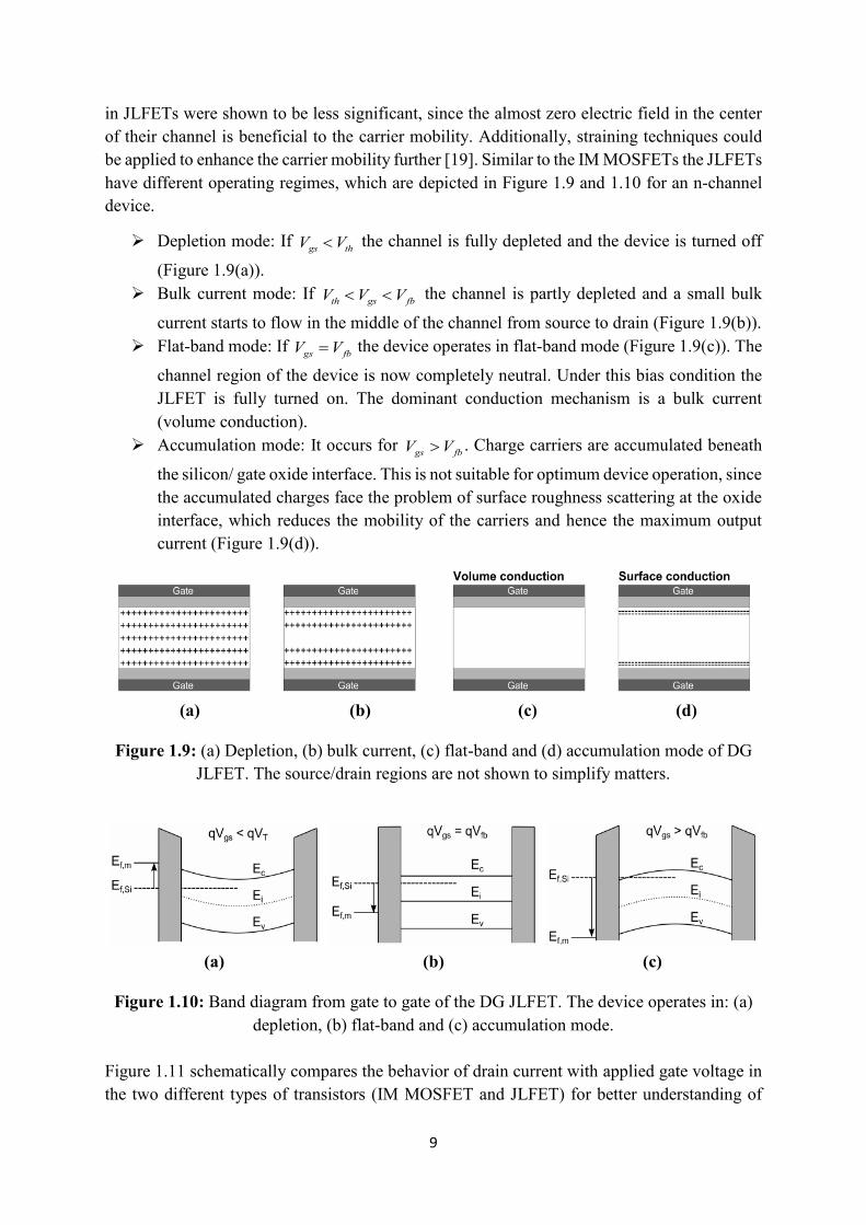
in JLFETs were shown to be less significant, since the almost zero electric field in the center of their channel is beneficial to the carrier mobility. Additionally, straining techniques could be applied to enhance the carrier mobility further [19]. Similar to the IM MOSFETs the JLFETs have different operating regimes, which are depicted in Figure 1.9 and 1.10 for an n-channel device.
Depletion mode: If gs thV V the channel is fully depleted and the device is turned off
(Figure 1.9(a)). Bulk current mode: If th gs fbV V V the channel is partly depleted and a small bulk
current starts to flow in the middle of the channel from source to drain (Figure 1.9(b)). Flat-band mode: If gs fbV V the device operates in flat-band mode (Figure 1.9(c)). The
channel region of the device is now completely neutral. Under this bias condition the JLFET is fully turned on. The dominant conduction mechanism is a bulk current (volume conduction).
Accumulation mode: It occurs for gs fbV V . Charge carriers are accumulated beneath
the silicon/ gate oxide interface. This is not suitable for optimum device operation, since the accumulated charges face the problem of surface roughness scattering at the oxide interface, which reduces the mobility of the carriers and hence the maximum output current (Figure 1.9(d)).
(a) (b) (c) (d)
Figure 1.9: (a) Depletion, (b) bulk current, (c) flat-band and (d) accumulation mode of DG JLFET. The source/drain regions are not shown to simplify matters.
(a) (b) (c)
Figure 1.10: Band diagram from gate to gate of the DG JLFET. The device operates in: (a) depletion, (b) flat-band and (c) accumulation mode.
Figure 1.11 schematically compares the behavior of drain current with applied gate voltage in the two different types of transistors (IM MOSFET and JLFET) for better understanding of

10
JLFETs operation. For inversion-mode device, the flat-band voltage which leaves the p-type body neutral, is located below threshold voltage. Above threshold voltage, a surface depletion layer is formed, with an inversion channel at the interface between silicon and gate oxide. In contrast, for JLFETs, flat-band voltage is above threshold voltage and the device is fully depleted below threshold voltage.
However, JLFETs are facing some issues such as mobility degradation by their high channel doping, reduced gate controllability due to partial depletion regions under gate insulator and threshold voltage variability induced by fluctuation of Si thickness and doping atoms spatial distribution [28]. Nevertheless, the extremely simple structure of JLFETs could lead them to be a feasible candidate for the realization of sub-22 nm CMOS technology.
(a) (b)
Figure 1.11: Drain current variation with gate voltage for (a) IM MOSFETs and (b) JLFETs [19].
1.2.2 State-of-the-Art-Junctionless Field Effect Transistors
A very important task is the development of models to describe the behavior of JLFETs in a physical manner. Different models and approaches were published, which warrant a discussion.
1.2.2.1 Models
F. Lime et al. presented a compact model for the junctionless (JL) DG MOSFET valid in all operating regimes in [27]. Their approach led to simple equations compared to other models, while the high accuracy and physical consistency was retained. The model reproduced the two discussed conduction modes well. In order to find closed-form expression for the current, they introduced some mathematical manipulations.
E. Gnani et al. proposed a model for JL nanowire FETs in [29], where the current was calculated in the separated operating regimes and then superposed. The device variability and the parasitic source/drain resistances were identified as the most important limitations of the JL nanowire FET.

11
J. M. Sallese et al. derived an analytical model for symmetric JL DG MOSFETs in [30]. By using charge-based expressions, a continuous current model was derived. The occurrence of two distinct slopes in the charge-voltage dependence, which constituted a major difference compared to junction-based MOSFETs, was well covered by their model. However, at this point, their results for the current showed inaccuracies in the depletion region, whose origins were yet not clarified.
A. Cerdeira et al. presented a new charge-based analytical compact model for symmetric DG JLFETs [31]. The model is physics-based and considers both the depletion and accumulation operating conditions including the series resistance effects.
Quantum mechanical effects (QMEs) were obtained under two different quantum confinement conditions in [32]. It was shown that the quantum confinement is higher in JL than in IM DG MOSFETs, regardless of the channel thickness. Nevertheless, this model is only valid in the subthreshold regime.
A physics-based model for the ultra-thin-body (UTB) SOI-FET, which is based on an improved depletion approximation and which provides a very accurate solution of Poisson’s equation was discussed in [33]. A computation method of the substrate, as well as the Si-body’s lower and upper surface potentials by an iterative procedure, which accounts for the buried oxide (BOX) charge and thickness and the potential drop within the substrate was presented.
The trade-off between the electrostatic control and the current drivability was evaluated by M. Berthomé et al. [34]. The focus was on various MOSFET architectures based on single gate (SG), double gate (DG) and gate-all-around (GAA) transistors. The model permits a first-order description of the drain current, the pinch-off and flat-band voltages.
A physics-based, analytical model for the drain current in junctionless nanowire transistors (JNTs) was addressed in [35]. The proposed model is continuous from the subthreshold region to the saturation. The derived charge density was expressed as the sum of charge densities in two separate channel regions, which were connected by using a smoothing function later on.
J. P. Duarte et al. presented a full-range drain current model for long-channel DG JLFETs in [36]. Including dopant and mobile carrier charges, a continuous 1-D charge model was derived by extending the concept of parabolic potential approximation for the subthreshold and the linear regions. Based on the charge model, the Pao-Sah integral was analytically carried out and a continuous drain current model was obtained.
J. Xiao-Shi et al. proposed a continuous model for the drain current of junctionless cylindrical surrounding-gate Si nanowire MOSFETs in [37]. The model is based on an approximated solution of Poisson’s equation considering both body doping and mobile charge concentrations and did not introduce any empirical fitting parameters.
Z. Chen et al. developed a surface potential based model for symmetric long-channel JL DG MOSFETs in [38]. The relations between surface potential and gate voltage were derived from effective approximations to Poisson’s equation for deep depletion, partial depletion and accumulation conditions. However, no closed-form expressions for the drain current were presented.

12
The depletion width equation was simplified by the unique characteristic of junctionless transistors (high channel doping concentration) in [39]. From the depletion width formula, the bulk current model was constructed using Ohm’s law. An analytical expression for subthreshold current was derived. The model was validated for different device setups.
F. Jazaeri et al. developed a closed-form solution for trans-capacitances in long-channel JL DG MOSFETs [40]. The model was derived from a coherent charge-based model. A complete intrinsic capacitance network was obtained, which represented an important step toward AC analysis of circuits, based on junctionless devices. The Ward-Dutton partitioning principle and a cubic function were applied to derive the model for the trans-capacitances.
R. D. Trevisoli et al. was focusing on the threshold voltage in JNTs and presented some analytical models for their description and an extraction method in [41] and [42], respectively. A simple modification to account for QMEs in such devices was included. The corner capacitances were addressed in their work, as well as temperature effects on the threshold voltage. The model was compared versus numerical and experimental data.
Y. Taur et al. discussed the on-off charge-voltage characteristics and dopant number fluctuation effects in JL DG MOSFETs in [43]. A first-order analytic expression showed that the one-sigma threshold fluctuation is proportional to the square root of doping concentration. They stated that the effect of dopant number fluctuations on the threshold voltage is a serious problem in JL devices, due to the high channel doping concentration.
An advanced model for DG structure of JLFET, where most parameters were related to physical magnitudes, was shown to be in excellent agreement with the simulation data [44]. The effect of the series resistance and the fulfillment of the requirement of being symmetrical with respect to 0dsV V was discussed.
So far, all mentioned models are only valid for long-channel devices (1-D), which clearly indicates the need for an analytical, physical compact model valid for short-channel JL devices (2-D) as well. Recently, some 2-D models were published for different device geometries. An analytical subthreshold behavior model for junctionless cylindrical surrounding gate MOSFETs was developed by C. Li et al. [45], whereby 2-D Poisson’s equation was solved in cylindrical coordinates. The subthreshold characteristics were investigated in terms of the channel’s electrostatic potential distribution, subthreshold current and slope.
A new quasi 2-D threshold voltage model valid for short channel junctionless cylindrical surrounding gate MOSFETs was proposed by T. K. Chiang [46]. It is based on the parabolic approximation for the potential and therefore, removed previous limitations. Relevant SCEs, such as threshold voltage roll-off and DIBL were evaluated.
A unified analytical current model for both n- and p-type junctionless surrounding-gate nanowire FETs valid from low to high doping concentrations is developed in [47]. The well-known charge-based model derived by extending the parabolic potential approximation to Poisson equation in the cylindrical coordinate system was used. Drain current dependencies on various device parameters were worked out and analyzed.

13
R. D. Trevisoli et al. proposed a drain current model for triple-gate n-type JNTs in [48]. First, the 2-D Poisson equation was used to obtain the effective surface potential for long-channel devices, which was used to calculate the charge density along the channel and the drain current. The solution of the 3-D Laplace equation was then added to the 2-D model in order to account for the SCEs. To obtain the drain current including SCEs, the surface potential was recalculated for a modified gate voltage (iteration).
In 2013 F. Jazaeri et al. [49] published a paper, where they present an analytical model for the electric potential, drain current and subthreshold swing of ultra-thin-body symmetric DG JLFETs in subthreshold region. They solved the 2-D Poisson equation using parabolic approximation in the channel region. The effects of variation of different device parameters on potential, SS and DIBL are also analyzed.
The 2-D models presented in [45–48] are only valid for JNT in subthreshold region. In [49] a complete 2-D analytical model was presented for DG JLFETs. However, their modeling approach is valid for only symmetric structure of DG JLFETs.
1.2.2.2 Technologies
A complete fabrication process of a junctionless multiple-gate MOSFET was detailed in [22], which is briefly reviewed here considering an n-channel transistor. The devices were made on a standard SOI wafer. The SOI layer was thinned down to 10−15 nm and patterned into nanowires using an e-beam lithography. After performing the gate oxidation, an ion implantation was used to dope the devices uniformly n+ with a concentration of 1 − 2×1019 cm−3. A p+ polysilicon gate was used. No additional source/drain implants were used after patterning the gate. The oxide was deposited and etched to form contact holes and a TiW + Al metalization completed the process. The nanowires were fabricated with thicknesses ranging from 5 to 10 nm, a width ranging from 20 to 40 nm and a gate oxide thickness of 10 nm. Similar devices with additional source/drain implants were also fabricated to reduce the parasitic access resistances, which improved the drain current.
Other groups dedicated their works to the impact of the series resistances in the current-voltage characteristics of JNTs and its dependence on the temperature [50]. A low-temperature electrical characterization of JL transistors was done by D. Y. Jeon et al. [51]. The electron mobility in heavily doped junctionless nanowire SOI MOSFETs was investigated in [52] and the electrical characteristics of JNTs at a channel length of 20 nm were studied in [53]. A parameter extraction methodology for electrical characterization of JLTs was presented in [54]. The impact of substrate bias on the steep subthreshold slope in junctionless multiple gate FETs was subject of [55]. An investigation of the zero temperature coefficient in JNTs was done by R. D. Trevisoli et al. [56] and a comparison of manufactured junctionless versus conventional triple gate transistors with channel lengths down to 26 nm was performed in [57]. Also, the variability of the drain current, induced by random doping fluctuation, of junctionless nanoscale double gate transistors was intensively investigated by G. Giusi et al. [58].
In 2014, C. Wan et al. [59] presented a study where the junctionless transistor was applied in the field of associative learning in neuromorphic engineering. Indium-zinc-oxide based

14
electric-double-layer junctionless transistors gated by nanogranular SiO2 proton conducting electrolyte films were proposed. They found out that such proton conductor gated transistors with associative learning functions are promising candidates in neuromorphic circuits.
For the first time, III-V junctionless transistors were experimentally demonstrated by Y. Song et al. [60]. The source/drain resistances and the thermal budget were minimized by using metal-organic chemical vapor deposition instead of an implantation process. The fabricated devices exhibited very good mg linearity at low biases, which is favorable for low-power RF applications.
1.3 Thesis Objectives When traditional planar MOSFETs are scaled, they lose the gate control over the channel charges because the charges are partially controlled by the drain/source depletion regions. Several types of nonplanar structures with multiple-gated configurations have been proposed for providing better electrostatic control of the charges in the channel region; therefore reducing SCEs – like SS degradation, threshold voltage roll-off (TVRO) and DIBL. However, further miniaturization of such devices becomes quite challenging because of the formation of ultra-shallow and abrupt junctions which requires novel doping and special annealing techniques. Recently JLFETs have become a better solution to this problem as they need neither lateral abrupt doping, nor high thermal budget, thus making manufacturing simpler. Besides that JLFETs provide reduced SCEs, an excellent SS, a very low leakage current and high Ion/Ioff ratio compared to conventional MOSFETs. A number of analytical studies based on 1-D models have been performed to anticipate the performance of long channel symmetric DG JLFET. However, a complete 2-D analytical treatment for both symmetric and asymmetric short channel DG JLFETs considering similar and dissimilar gate biased configuration is necessary to make a comparative study of their performance. The objectives of this work are:
To obtain analytical expression for 2-D electrostatic potential of DG JLFETs applicable for both symmetric and asymmetric structures in the subthreshold region.
To develop simulators using SILVACO ATLAS and COMSOL Multiphysics 3.5 in order to verify the proposed potential model.
To evaluate threshold voltage, current-voltage (I-V) characteristics and different SCEs such as, TVRO, DIBL, SS for different structures using the potential model.
To make a comparative study of performance in the subthreshold region for different structures of JLFETs.
In order to obtain analytical expression of electrostatic potential in the subthreshold region, we will analytically solve 2-D Poisson’s equation in the channel region using cubic approximation with appropriate boundary conditions. Then we will determine threshold voltage by finding the gate voltage for which the minimum channel potential along the length of the device is zero. We will calculate TVRO, DIBL, I-V characteristics and SS numerically using MATLAB to avoid extensive mathematical complexity from the potential model. In order to verify the obtained results from the analytical model we will develop 2-D device simulators using

15
SILVACO ATLAS and COMSOL Multiphysics 3.5. We will compare potential profile, I-V characteristics, SCEs viz. TVRO, DIBL and SS for similar-dissimilar gate biased and symmetric-asymmetric structures of JLFETs.
1.4 Thesis Organization The entire thesis is broadly divided into five chapters and a brief outline of each chapter is described below.
The first chapter is an introduction to the continuous need for scaling down of MOSFETs and recent advancements in the semiconductor industries. Different short channel effects associated with device miniaturization are also studied which necessitates the alternative device structures to overcome the barriers of bulk MOSFET. This introductory chapter also includes the motivation to this work and important highlights followed by a brief overview of JLFET and current literature about the field of this work.
The second chapter considers the structure and develops a 2-D channel potential model for DG JLFET operating in the subthreshold region. The model takes into account the vital role of various JLFET parameters like the channel length, silicon and gate dielectric thickness, flat-band voltages of gate electrodes, applied gate to source and drain to source biases, in influencing the channel potential. Based on this potential model established, methods of evaluating the threshold voltage, DIBL, subthreshold current and SS are discussed.
The third chapter discusses about the numerical simulation techniques used to justify the validity of the proposed model. Numerical simulation incorporates a 2-D simulation model using both SILVACO ATLAS – a widely used technology computer-aided design (TCAD) tool and COMSOL Multiphysics 3.5.
The fourth chapter presents the results obtained from both the analytical and numerical methods. Verification of the results obtained from proposed analytical model has been performed by that from simulation model. A comparative study of SCEs for different structures of JLFETs is also presented in this chapter.
The fifth chapter draws the conclusion of my entire thesis. It also mentions the scopes for further improvement of the work and provides a suggestion of possible areas which can be explored in future.

16
Chapter 2 Analytical Model Development For the fast developing devices and circuits, reliable and predictive analytical models are required. In this chapter, the analytical model of 2-D electrostatic potential in the channel region for a DG JLFET is developed. Here, a step by step detailed mathematical description of the proposed model along with the device structure is presented. First, 2-D Poisson’s equation in the channel region with appropriate boundary conditions is solved using cubic approximation. Then the obtained expression for potential distribution is used to calculate threshold voltage, DIBL, drain current and SS.
2.1 Device Structure The schematic cross-sectional view of an n-type DG JLFET used in the analytical modeling is shown in Figure 2.1. The X- and Y-axes shown in the figure indicate the source to drain and the top to bottom gate directions respectively, with the origin set at the intersection of the source and top gate oxide/channel interface. The thickness of the source and drain regions are assumed to be zero for the sake of simplicity of modeling. The source and drain electrodes are shown to be present at the two side of the bulk silicon layer which is heavily doped with n-type impurity. The device is assumed to have a channel length of gL , channel thickness of sit , top and bottom
gate oxide thickness of 1oxt and
2oxt . 1gsV and
2gsV are the top and bottom gate bias respectively.
The source is connected to zero potential and dsV is applied at the drain terminal.
Figure 2.1: Schematic cross-sectional view of a DG JLFET.

17
2.2 Electrostatic Potential Modeling 2.2.1 Poisson Equation
The proposed analytical model of electrostatic potential of DG JLFET is about anticipating the characteristics of the device in the subthreshold regime. The channel region is assumed to be perfectly depleted in the subthreshold operation regime and the impact of mobile charge on the channel potential is negligible. For simplicity, fixed oxide charges at oxide/silicon interfaces are neglected. Under these aforementioned simplification, the potential profile of the proposed device can be calculated by solving 2-D Poisson’s equation in the channel region. Then, the 2-D Poisson’s equation for n-channel DG JLFET can be expressed as,
2 2
2 2
( , ) ( , ) d
si
qNx y x yx y
00
g
si
x Ly t
(2.1)
where ( , )x y is the 2-D channel potential, q is the elementary charge, dN is the uniform
doping concentration in the channel region and si is the dielectric constant of silicon.
2.2.2 Cubic Approximation
In order to evaluate a generalized potential profile in the channel region applicable for both symmetric and asymmetric DG JLFET with similar and dissimilar gate biased condition, a cubic potential distribution is assumed along the top to bottom gate direction which can be expressed as,
2 30 1 2 3( , ) ( ) ( ) ( ) ( )x y c x c x y c x y c x y
00
g
si
x Ly t
(2.2)
The coefficients 0 ( )c x , 1( )c x , 2 ( )c x and 3( )c x are function of x only and are solved using the appropriate boundary conditions.
2.2.3 Boundary Conditions
The 2-D Poisson’s equation can be solved by considering cubic potential profile in the channel region using following boundary conditions.
The surface potentials of the channel at the top/bottom gate oxide and silicon channel interface are given by:
10
( , ) ( )syx y x
(2.3)
2( , ) ( )
sisy t
x y x
(2.4)

18
According to the Gauss’s law, the electrical flux between the silicon channel and top/bottom gate oxide must be continuous. So the electric fields at the top/bottom gate oxide and channel interface are given as:
1 1 1 1 1 1 1
1 10
( ) ( )( , ) ox s gs fb ox s gs
si ox si oxy
x V V x Vx yy t t
(2.5)
2 2 2 2 2 2 2
2 2
( ) ( )( , )
si
ox gs fb s ox gs s
si ox si oxy t
V V x V xx yy t t
(2.6)
Here 1ox and
2ox are the permittivity of the top and bottom gate oxide respectively. The
effective top and bottom gate biases are 1 1 1gs gs fbV V V and
2 2 2gs gs fbV V V
respectively. The flat-band voltages at the interface of the silicon body and top/bottom gate electrodes are
1 1fb m sV and 2 2fb m sV where
1m and 2m are the work-
function of the top and bottom gate electrodes, respectively. s is the silicon work function and for n-type doping it can be written as,
g ds s t
i
E N=χ + -V ln2q n
(2.7)
where tV is the thermal voltage, sχ is the electron affinity, gE is the bandgap energy
and in is the intrinsic carrier concentration of silicon. The boundary conditions of potential at the source and drain terminal of the device are
as follows,
0( , ) 0
xx y
(2.8)
( , )
gdsx L
x y V
(2.9)
2.2.4 Coefficients Determination
The coefficients 0 ( )c x and 1( )c x of (2.2) can be directly obtained by using the boundary conditions mentioned in (2.3) and (2.5) which can be expressed as,
10 ( ) ( )sc x x (2.10)
1
1 1
1
1( ) ( )oxs gs
si ox
c x x Vt
(2.11)
Now applying the boundary condition mentioned in (2.4) and then substituting 0 ( )c x and 1( )c xfrom (2.10) and (2.11) respectively, the relation between 2 ( )c x and 3( )c x can be found as,

19
1 1
1 2 1
1 1
2 3 2 2
1 1( ) ( ) ( ) ( )ox oxsi s s gs
si si ox si si si ox si
c x c x t x x Vt t t t t t
(2.12)
Similarly using the boundary condition mentioned in (2.6) and then replacing 1( )c x from
(2.11), another relation between 2 ( )c x and 3( )c x can be obtained as,
1 2 1 2
1 2 1 2
1 2 1 2
2 32 ( ) 3 ( ) ( ) ( )ox ox ox oxsi s s gs gs
si ox si si ox si si ox si si ox si
c x c x t x x V Vt t t t t t t t
(2.13)
Now by solving (2.12) and (2.13), the remaining coefficients 2 ( )c x and 3( )c x of (2.2) can be determined as,
1 2
2 1 1 1 2 2
1 2
2 2
23( ) ( ) ( ) ( ) ( )ox oxs s s gs s gs
si si ox si si ox si
c x x x x V x Vt t t t t
(2.14)
1 2
1 2 1 1 2 2
1 2
3 3 2 2
2( ) ( ) ( ) ( ) ( )ox oxs s s gs s gs
si si ox si si ox si
c x x x x V x Vt t t t t
(2.15)
After substituting the coefficients 0 ( )c x , 1( )c x , 2 ( )c x and 3( )c x from (2.10), (2.11), (2.14) and (2.15) in (2.2), the 2-D electrostatic potential profile in the channel region can be written as,
1
1 1 1
1
1 2
2 1 1 1 2 2
1 2
1 2
1 2 1 1 2 2
1 2
22
3 2 2
( , ) ( ) ( )
23 ( ) ( ) ( ) ( )
2 ( ) ( ) ( ) ( )
oxs s gs
si ox
ox oxs s s gs s gs
si si ox si si ox si
ox oxs s s gs s gs
si si ox si si ox si
x y x x V yt
x x x V x V yt t t t t
x x x V x Vt t t t t
3y
(2.16)
2.2.5 Capacitance Model
The 2-D channel potential profile mentioned in (2.16) depends on two unknown quantities: top surface potential (
1( )s x ) and bottom surface potential (
2( )s x ). In order to find a solution of
potential distribution in the channel region from 2-D Poisson’s equation, first it has to be converted into 1-D differential equation. For this reason a 1-D capacitance model has been assumed along the top to bottom gate direction for DG JLFET in the subthreshold region so that a correlation between
1( )s x and
2( )s x can be obtained. In this capacitance model the
device is assumed to have three series capacitors which is derived from the two terminal structure of DG JLFET shown in Figure 2.2. The series capacitances are top gate oxide capacitance (
1oxC ), silicon body capacitance ( siC ) and bottom gate oxide capacitance (2oxC ).

20
Figure 2.2: (a) Two terminal structure and (b) 1-D capacitance model of DG JLFET
in the subthreshold region.
The silicon channel of DG JLFET is fully depleted by flat band voltage induced by the work-function difference between the gate electrode and silicon body in the subthreshold region. The threshold voltage is reached when a portion of the channel is no longer depleted, such that bulk current flows through a neutral path. So when gate to source voltage is less then threshold voltage the depletion region thickness hence the capacitance of the silicon channel remains constant. But when the gate voltage is raised above the threshold voltage the depth of the depletion region decreases. So the silicon capacitance does not remain constant. As we are modeling a potential profile in the subthreshold region the capacitance model is assumed to be accurate. From the capacitance model the relation between two surface potentials of the device can be found as,
1 2
1 2 1 2
1 1 2 2
( ) ( ) ox oxs s gs gs
ox si ox ox si ox
C Cx x V V
C C C C C C
(2.17)
Finally putting the values of 1oxC , siC and
2oxC in (2.17) 2( )s x can be expressed in terms of
1( )s x as follows,
1 2
2 1 1 2
1 2 1 2 2 1
( ) ( ) ox ox sis s gs gs
ox si ox ox ox si si ox ox
tx x V V
t t t
(2.18)
Substituting 2( )s x from (2.18) into (2.16) the potential function in the channel in terms of top
surface potential 1( )s x can be found as,
(a) (b)

21
1 1 2 1 2 1
1 1
1 1 2 1 2 1
1 2 2 21 2
1 2
1 2
2 32
21 1( , ) ( ) 1
31 2
ox ox ox ox ox oxs gs
si ox si si ox ox si si ox ox si ox
ox ox si ox ox siox oxgs gs
si si ox ox si
x y x y y y V yt t t t t t t t
t tV V
t t t t
1 2
2 1 2 1 2 2 1
1 2 2 21 2
1 2 1 2
1 2 2 1 2 1 2 2 1
2
2 2
21
gs gsox si ox si ox ox ox si si ox ox
ox ox si ox ox siox oxgs gs gs gs
si si ox ox si ox si ox si ox ox ox si si ox ox
V V yt t t t
t tV V V V
t t t t t t t t
3y (2.19)
2.2.6 Channel Potential
The inherent behavior of the JLFET is volume conduction mode in contrast to a conventional junction based MOSFET with surface conduction mode. So the 2-D potential profile mentioned in (2.19) in term of surface potential at the top gate oxide and silicon channel interface provides very limited information for understanding the whole channel potential of short channel DG JLFET. The potential distribution at an arbitrary depth should be found because a comprehensive model of the potential distribution in the entire channel region is very useful for a microscopic analysis. The 1-D potential line along the source to drain direction at an arbitrary depth y Y in the channel region is defined as,
( ) ( , )Y y Yx x y
(2.20)
So the relation between 1( )s x and ( )Y x can be obtained from (2.19) and (2.20).
1
1 1 2 1 2
1 1 2 1 2
1 2
1 2
1 21
1
1 1 2 2 2
2 32
1( )21 11
1 2
( )3
sox ox ox ox ox
si ox si si ox ox si si ox ox
ox oxgs gs
si si ox oxoxY gs
si ox ox ox si ox ox si
si
x
Y Y Yt t t t t t t
V Vt t t
x V Yt t t
t
1 2
2 1 2 1 2 2 1
1 2 2 21 2
1 2 1 2
1 2 2 1 2 1 2 2 1
2
2 2
21
gs gsox si ox si ox ox ox si si ox ox
ox ox si ox ox siox oxgs gs gs gs
si si ox ox si ox si ox si ox ox ox si si ox ox
Y
V Vt t t t
t tV V V V
t t t t t t t t
3Y
(2.21)
Now the 2-D potential function in term of ( )Y x can be found by substituting 1( )s x from
(2.21) into (2.19).

22
1 1 2 1 2
1 1 2 1 2
1 1 2 1 2
1 1 2 1 2
2 32
2 32
21 11( , )
21 11
( )
ox ox ox ox ox
si ox si si ox ox si si ox ox
ox ox ox ox ox
si ox si si ox ox si si ox ox
Y
y y yt t t t t t t
x yY Y Y
t t t t t t t
x
1 2 2 21 1 2
1 1 2 1 2
1 1 2 2 1 2 1 2 2 1
1 2
1 2
1 2
2
2
31 2
1
ox ox si ox ox siox ox oxgs gs gs gs gs
si ox si si ox ox si ox si ox si ox ox ox si si ox ox
oox oxgs gs
si si ox ox
t tV Y V V V V Y
t t t t t t t t t
V Vt t t
1 2 2 2
1 2
2 1 2 1 2 2 1
1 2 2 21 1 2
1 1 2
1 1 2
32
2
31 2
x ox si ox ox sigs gs
si ox si ox si ox ox ox si si ox ox
ox ox si ox ox siox ox oxgs gs gs
si ox si si ox ox si ox
t tV V Y
t t t t t
t tV y V V
t t t t t
1 2
2 1 2 1 2 2 1
1 2 2 21 2
1 2 1 2
1 2 2 1 2 1 2 2 1
2
32 2
21
gs gssi ox si ox ox ox si si ox ox
ox ox si ox ox siox oxgs gs gs gs
si si ox ox si ox si ox si ox ox ox si si ox ox
V V yt t t t
t tV V V V y
t t t t t t t t
(2.22)
By substituting (2.22) in (2.1) the 2-D Poisson’s equation can be reduced to a simple 1-D second order nonhomogeneous differential equation for the potential distribution at any arbitrary depth y Y along the silicon channel as follows,
1 2 1 2
1 2 1 2
1 1 2 1 2
1 1 2 1 2
1
1
22
22 3
2
22 6( )
21 11
( )
ox ox ox ox
si si ox ox si si ox oxY
ox ox ox ox ox
si ox si si ox ox si si ox ox
oxg
si ox
Y
Yt t t t t tx
xY Y Y
t t t t t t t
Vt
x
1 2
1 2
1 2
1
1 2 2 2
1 2
2 1 2 1 2 2 1
11 2
1 2
1 2
2
2
1 2
3
1
ox oxgs gs
si si ox ox
sox ox si ox ox si
gs gssi ox si ox si ox ox ox si si ox ox
ox oxox oxgs gs
si si ox ox
V Vt t t
Y Yt t
V Vt t t t t
V Vt t t
2 2 2
1 2
2 1 2 1 2 2 1
1 2 21 2
1 2
1 2
32
2
2 32 2
si ox ox sigs gs
si ox si ox si ox ox ox si si ox ox
ox ox si ox oxox oxgs gs
si si ox ox
t tV V Y
t t t t t
tV V
t t t
2
1 2
2 1 2 1 2 2 1
1 2 2 21 2
1 2 1
1 2 2 1 2 1 2 2 1
2 2
6 26
si dgs gs
sisi ox si ox si ox ox ox si si ox ox
ox ox si ox ox siox oxgs gs gs
si si ox ox si ox si ox si ox ox ox si si ox ox
t qNV Vt t t t t
t tV V V
t t t t t t t t
2
0
gsV Y
(2.23)
Equation (2.23) can be rewritten as,
2
2 2
( ) 1 ( ) 0YY Y
Y
x xx
(2.24)

23
where,
1 1 2 1 2
1 1 2 1 2
1 2 1 2
1 2 1 2
2 32
2
21 11
22 6
ox ox ox ox ox
si ox si si ox ox si si ox oxY
ox ox ox ox
si si ox ox si si ox ox
Y Y Yt t t t t t t
Yt t t t t t
(2.25)
2
Y Y Y Y (2.26)
with,
1 2
1 2
1 21
1
1 1 2 2 2
1 2
2 1 2 1 2 2 1
1 2
1
1 2
2
2
1 2
3
1
ox oxgs gs
si si ox oxoxY gs
si ox ox ox si ox ox sigs gs
si ox si ox si ox ox ox si si ox ox
ox oxgs g
si si ox ox
V Vt t t
V Y Yt t t
V Vt t t t t
V Vt t t
1 2 2 2
2 1 2
2 1 2 1 2 2 1
32
2ox ox si ox ox sis gs gs
si ox si ox si ox ox ox si si ox ox
t tV V Y
t t t t t
(2.27)
1 2 2 21 2
1 2 1 2
1 2 2 1 2 1 2 2 1
1 2 21 2
1 2
1 2
2
2 32 2
6 26
ox ox si ox ox siox ox dY gs gs gs gs
si si ox ox sisi ox si ox si ox ox ox si si ox ox
ox ox si ox oox oxgs gs
si si ox ox
t t qNV V V Vt t t t t t t t
tV V
t t t
2
1 2
2 1 2 1 2 2 1
2
x sigs gs
si ox si ox si ox ox ox si si ox ox
tV V Y
t t t t t
(2.28)
The general solution of the ordinary differential equation of ( )Y x mentioned in (2.24) can be obtained as,
( ) Y Y
x x
Y Y Y Yx e e
(2.29)
Applying the boundary conditions near source and drain terminal of the device mentioned in (2.8) and (2.9) the general solution can be written as,
0Y Y Y (2.30)
g g
Y Y
L L
Y Y Y dse e V
(2.31)
By solving (2.30) and (2.31) the coefficients Y and YB can be determined as,

24
1g
Y
g g
Y Y
L
ds Y
Y L L
V e
e e
(2.32)
1g
Y
g g
Y Y
L
ds Y
Y L L
V e
e e
(2.33)
Since the potential function in (2.29) is obtained for any arbitrary depth y Y in the channel,
the distribution is also valid for an arbitrary position ,x y in the entire channel. Therefore,
the 2-D channel potential distribution ( , )x y can be obtained by substituting the values of Y
and YB from (2.32) and (2.33) and then replacing Y with y in (2.29).
sinh sinh( , )
sinh
gds y y
y yy
g
y
L xxVx y
L
(2.34)
2.3 Threshold Voltage and DIBL Calculation For a normally off DG JLFET, the increasing gate voltages will conduct the channel that is pinched off by the flat-band voltages induced by the work-function difference between the gate electrodes and silicon body. The majority carriers of the device essentially flow in the volume of the silicon channel. The voltage at which the device is turned on, is called threshold voltage. Below threshold, the potentials at the surfaces of the device are lower than that of the channel region. In order to determine the threshold voltage, first the depth of the silicon channel along the top to bottom gate direction is determined at which the potential is maximum. The line along source to drain direction at that particular depth of the silicon channel represents the leakiest pathway between source and drain. When the minimum potential at that particular depth becomes zero, a neutral path with bulk silicon is opened along that line in the channel from source to drain direction. So the gate voltage for which minimum potential along the line at that particular depth from source to drain direction becomes zero, represents the threshold voltage [46]. In order to avoid analytical complexity in this work we determine threshold voltage of different structures of JLFET numerically by MATLAB from the 2-D channel potential mentioned in (2.34).
Threshold voltage becomes a function of drain to source voltage for the short channel DG JLFET. Drain induced barrier lowering (DIBL) can be defined as the lowering in the threshold voltage due to the increase in the drain voltage [61]. If the threshold voltages of the device are

25
LthV for low drain voltages LdsV and
HthV for high drain voltages HdsV , then DIBL can be expressed
as,
L H
H L
th thth
ds ds ds
V VVDIBLV V V
(2.35)
In this work for DIBL calculation we choose the value of low drain voltage and high drain voltage as
LdsV = 0.1V and HdsV = 1V respectively.
2.4 Drain Current and Subthreshold Swing Calculation
With the analytical 2-D electric potential ( , )x y expressed in (2.34), subthreshold current can be calculated as [49],
( , )0
0
1ds
t
g
si
t
VV
n t
ds L
x ytV
i
q WV e
Idx
n e dy
(2.36)
where n and W are the effective carrier mobility of silicon and channel width respectively. In this work to avoid computational complexity subthreshold current is obtained by numerical integration from the 2-D electrostatic potential using MATLAB.
Subthreshold swing (SS) of DG JLFET can be obtained by numerical differentiation of subthreshold current extracted from (2.36) using following equation [49].
10loggs
ds
VSS
I
(2.37)

26
Chapter 3 Simulation Model Development The significance of modeling semiconductor devices using different simulators are increasing day by day because they make a drastic reduction in testing time and costs involved in the fabrication processes of the devices. The focus of this thesis is not to offer the details on numerical simulation techniques for JLFET rather this work will use the numerical tools as an effective way to verify the developed analytical solution. In this chapter two simulation models have been developed in SILVACO ATLAS and COMSOL Multiphysics 3.5, to check the validity of the proposed model. A detailed description of various commands and their contextual meaning are also presented in this chapter.
3.1 SILVACO ATLAS Technology Computer Aided Design (TCAD) tools are used to automate electronic device design and allows modeling of semiconductor fabrication and semiconductor device operation. They are widely used in semiconductor device simulation for prediction, analysis and test purpose. Modeling device fabrication includes modeling different process steps such as ion implantation and diffusion. TCADs are also very useful to simulate the behavior of electronic devices and to model them based on their underlying fundamental physics. TCADs also allows to create compact models such as for transistors. Many TCAD tools are available nowadays. They provide facilities to simulate a wide number of semiconductor devices.
Silicon Valley Company (SILVACO) is a leading vendor in TCAD. Established in 1984 and located in Santa Clara, California, SILVACO has developed a number of exceptional CAD simulation tools to aid in semiconductor process and device simulation. SILVACO has an extensive support team to assist with the broad area of semiconductor technologies. The ability to accurately simulate a semiconductor device is critical to industry and research environments. The ATLAS device simulator from SILVACO Inc. is specifically designed for 2-D and 3-D modeling to include electrical, optical and thermal properties within a semiconductor device. ATLAS provides an integrated physics-based platform to analyze DC, AC and time-domain responses for all semiconductor-based technologies. The powerful input syntax allows the user to design any semiconductor device using both standard and user-defined material of any size and dimension. ATLAS also offers a number of useful device examples to assist one’s unique design.
Figure 3.1 shows the types of information that flow in and out of ATLAS. Most ATLAS simulations use two input files. The first input file is a text file that contains commands for ATLAS to execute. The second input file is a structure file that defines the structure that will be simulated. ATLAS produces three types of output files. The first type of output file is the run-time output, which gives the progress and the error and warning messages as the simulation proceeds. The second type of output file is the log file, which stores all terminal voltages and

27
currents from the device analysis. The third type of output file is the solution file, which stores 2-D and 3-D data relating to the values of solution variables within the device at a given bias point [62].
Figure 3.1: ATLAS inputs and outputs [62].
3.1.1 ATLAS Commands
For simulating any semiconductor device, a list of commands has to be delivered to ATLAS. These statements have to follow a certain order so that ATLAS can generate the device after execution. To run ATLAS in the DeckBuild environment, the user must first call the ATLAS simulator with the command,
go atlas
Once ATLAS is called there is a syntax structure that must be followed in order for ATLAS to execute the command file successfully. Table 3.1 shows a list of primary group and statement structure specifications. Although there are a few exceptions, the input file statements follow the general format of,
<statement> <parameter>=<value>
The order in which statements occur in an ATLAS input file is important. There are five groups of statements that must occur in the correct order. Otherwise, an error message will appear, which may cause incorrect operation or termination of the program. For example, if the material parameters or models are set in the wrong order, then they may not be used in the calculations. The order of statements within the mesh definition, structural definition and solution groups is also important.

28
Table 3.1: ATLAS command groups [62].
Groups Statements
Structure Specification
Mesh Region Electrode Doping
Material Models Specification
Material Model Contact Interface
Numerical Method Selection Method
Solution Specification
Log Solve Load Save
Results Analysis Extract Tonyplot
3.1.2 Structure and Model Development
A device structure is specified when the mesh, region, electrodes and doping are explicitly defined for simulation. Afterwards, the created device can be simulated by incorporating the desired physical models and numerical methods. The steps only those necessary for the development and readability of this thesis will be discussed here.
3.1.2.1 Mesh
The mesh is a grid of horizontal and vertical lines over the dimensions of the device. Like finite element simulation, this inverted cartesian gridlines area is used to define data points and solution points. The x-axis is positive from left to right, the y-axis is negative from bottom to top. The reason for the inverted y-axis is that the manufacturing coordinates are usually described as depth below the surface. All coordinates are entered in microns. The general format of defining the mesh is given below.
mesh space.mult=<value>
x.mesh location=<value> spacing=<value>
y.mesh location=<value> spacing=<value>
The space.mult parameter value is used as a scaling factor for the mesh created by the x.mesh and y.mesh statements. The default value is 1. Values greater than 1 will create a globally coarser mesh for fast simulation. Values less than 1 will create a globally finer mesh for increased accuracy. The x.mesh and y.mesh statements are used to specify the locations in microns of vertical and horizontal lines respectively, together with the vertical or horizontal

29
spacing associated with that line. At least two mesh lines must be specified for each direction. ATLAS automatically inserts any new lines required to allow for gradual transitions in the spacing values between any adjacent lines. The x.mesh and y.mesh statements must be listed in the order of increasing x and y. Both negative and positive values of x and y are allowed.
Figure 3.2 shows the mesh of a DG JLFET. The accuracy of any calculated value in ATLAS is dependent on the refinement of the mesh at the junction of interest. The x.mesh and y.mesh is much finer in the region under the gates to have a better calculation at that areas.
Figure 3.2: Mesh creation for DG JLFET.
3.1.2.2 Region
The region statement is used to separate the initial mesh statement into distinct blocks and sets the initial material parameters that can be referred to later by region number. Once the mesh is specified, every part of it must be assigned a material type using region statement. The general syntax of this command is,
region number=<integer> material=<material type> <position
parameters>
Region numbers must start at 1 and are increased for each subsequent region statement. ATLAS allows the user to define up to 200 different regions. The position parameters are specified in microns using the x.min, x.max, y.min and y.max parameters. If the position parameters

30
of a new statement overlap those of a previous region statement, the overlapped area is assigned as the material type of the new region. Make sure that materials are assigned to all mesh points in the structure. The material type relates physical parameters with the materials assigned to the mesh. The important material parameters for most standard semiconductors are already defined by ATLAS and therefore do not require any changes. We utilized the extensive model libraries in ATLAS since the developed JLFET were based in Si which is very well researched and documented. Figure 3.3 shows different regions of DG JLFET in SILVACO ATLAS.
Figure 3.3: Different regions of DG JLFET.
3.1.2.3 Electrode
Electrodes are the external electrical contacts. Once the regions are set, the electrodes must be assigned to the desired region so that it can be electrically analyzed. The electrodes can be assigned to any region or portion of a region. ATLAS has some fixed names for electrodes e.g. anode, cathode, gate, source and drain. The following statements were used to define these parameters.
electrode name=<electrode name> <position parameters>
The position parameters are specified in microns using the x.min, x.max, y.min and y.max parameters. ATLAS allows the user to specify up to 50 electrodes. Multiple electrode statements may have the same electrode name. Nodes that are associated with the same

31
electrode name are treated as being electrically connected. Different electrodes of DG JLFET are shown in Figure 3.4.
Figure 3.4: Different electrodes of DG JLFET.
3.1.2.4 Doping
The doping statement is used to assign the doping level within the previously assigned regions. Various properties can be appended to the doping statement to specify how the semiconductor is doped and of whether the region is n or p type. The following statements were used to define doping parameters.
doping <distribution_type> <dopant_type> <position_parameters>
concentration=<value>
Analytical doping profiles can have Uniform or Gaussian forms. The position parameters x.min, x.max, y.min and y.max can be used instead of a region number. Doping concentration of a particular region can be defined using concentration statement. Doping concentration in different regions of DG JLFET is shown in Figure 3.5.

32
Figure 3.5: Net doping in different regions of DG JLFET.
3.1.2.5 Contact
The contact statement is used to specify the work-function of the contact material. To introduce the contacts the following syntax is required.
contact name=<contact name> workfunction=<value>
Here name of the contact is given by contact name whereas its work-function is specified by value. Instead of specifying the work-function it can also be specified by their name in the contact statement for the commonly used contacts like n.polysilicon, p.polysilicon, aluminium, tungsten etc. In this case the statement will be as follows.
contact name=<contact name> <contact material>
The contact statement can also be used for shorting the two gates. These can be also done by naming the two electrodes same. Two gates are shorted by this statement for double gate structure.
contact name=<contact name> common=<contact name>
3.1.2.6 Model
The model statement is essential to the accurate modeling of a particular phenomenon because it sets flags for ATLAS to indicate the inclusion of different mathematical models, physical

33
mechanisms and other global parameters such as substrate temperature. Statement for models used in this work is as follows.
models bgn conmob cvt print
The description of different model parameters used in this work is given below.
bgn defines band-gap-narrowing. Since the doping variation that will be used in this analysis is very high, the p-n product in silicon will become doping dependent. As the doping level increases, a decrease in the band-gap is inevitable, where the conduction band is lowered by approximately the same amount as the valence band is raised.
conmob is used for concentration-dependent-mobility. The local electric field, lattice temperature, doping variation, surface and material imperfection inside the device will affect the mobility of the carriers.
cvt is used for activating the inversion layer model from Lombardi. In this model, Matthiessen’s rule is used for combining the components associated with mobility dependent on transverse field, temperature and doping. On activating this model by default, parallel electric field mobility model will also get activated.
print is used to specify the details of material parameters, constants and mobility models at the start of the run-time output. This is a useful way of checking what parameters values and models are being applied in the simulation.
3.1.3 Numerical Method Selection
Numerical methods are used to calculate solutions to semiconductor devices problems. The syntax for method used in this work is given below.
method newton
The newton method is useful when the system of equations are strongly coupled and has quadratic convergence. It may however spend extra time solving for quantities which are essentially constant or weakly coupled. It also requires a more accurate initial guess to the problem to obtain convergence.
3.1.4 Output Specification
Several quantities are saved by default within a structure file, for example doping, electron concentration and potential profile. We specified additional quantities such as conduction band potential, valence band potential by using the output statement.
output con.band val.band band.temp band.param

34
3.1.5 Solution Specification
Once the structure, physical model and numerical methods are set correctly, it is quite easy to extract the solution at each node points. The solve/save/log statements are used to create data files in ATLAS simulations. These statements work together to provide data to be analyzed by other functions. The solve statement specifies which bias points are to be applied to produce an output. The bias points can be set in a number of different way including step, initial and final value depending on what stimulus is desired. Initial solution can also be achieved by solve init statement. The save statement is used to save all node point data into an output file. With the data stored in an outfile, it is ready to be displayed so that it can be analyzed. The log statement allows all terminal characteristics generated by a solve statement to be saved to a file. It consist of the current and voltages for each electrode during the DC simulations. In transient simulations, the time is saved. Whereas for AC simulations, the conductance, capacitances and the small signal frequency are stored. For example, to get the solved structure and potential profile of DG JLFET, the following code is enough.
solve init
solve v<electrode name>=<value>
save outf=JLFET_structure.str
The ATLAS code for obtaining the drain current for different bias voltages is given below.
solve v<electrode name>=<value> vstep=<value> vfinal=<value>
name=<electrode name>
log outf=JLFET_current.log
save outf=JLFET_current.str
3.1.6 Results
After the simulation have been done a number of different other parameters can be observed. The tonyplot statement is used to start the graphical post-processor tool. The statements in ATLAS to obtain the structure, potential profile and current-voltage characteristics are as follows.
tonyplot JLFET_structure.str
tonyplot JLFET_current.log
By drawing a cutline along an arbitrary direction specified by two points in the x-y plane, we can examine the variation of several important parameters such as electric field, potential, conduction band energy, valance band energy etc. along the direction of cutline. Figure 3.6, 3.7, 3.8 show the complete structure of DG JLFET, potential profile along top to bottom gate and source to drain direction through the channel respectively.
In order to obtain the drain current of DG JLFET in the subthreshold region the simulated data from ATLAS is first extracted and then plotted in MATLAB. The drain current-gate voltage characteristics of DG JLFET is given in Figure 3.9.

35
Figure 3.6: 2-D structure of DG JLFET developed in SILVACO ATLAS.
Figure 3.7: Potential of symmetric DG JLFET along top to bottom gate direction for dsV =
0.1V and gsV = 0V considering gL = 50nm, sit = 10nm, 1oxt =
2oxt =1.5nm and dN = 1019cm-3.

36
Figure 3.8: Potential of symmetric DG JLFET along source to drain direction for dsV = 0.1V
and gsV = 0V considering gL = 50nm, sit = 10nm, 1oxt =
2oxt = 1.5nm and dN = 1019cm-3.
Figure 3.9: Current-voltage characteristics of symmetric DG JLFET for dsV = 0.1V
considering gL = 50nm, sit = 10nm, 1oxt =
2oxt = 1.5nm and dN = 1019cm-3.
0 0.2 0.4 0.610
-16
10-13
10-10
10-7
Gate to Source Voltage, Vgs
(V)
Dra
in C
urr
en
t, I
ds (
A/
m)

37
3.2 COMSOL Multiphysics COMSOL Multiphysics is a powerful interactive environment for modeling and solving all kinds of scientific and engineering problems based on partial differential equations (PDEs). With this product one can easily extend conventional models for one type of physics into multiphysics models that solve coupled physics phenomena and do so simultaneously. Accessing this power does not require an in-depth knowledge of mathematics or numerical analysis. The built-in physics modes is used to build models by defining the relevant physical quantities—such as material properties, loads, constraints, sources, and fluxes—rather than by defining the underlying equations. COMSOL Multiphysics then internally compiles a set of PDEs representing the entire model. One can access the power of COMSOL Multiphysics as a standalone product through a flexible graphical user interface or by script programming in the COMSOL Script language or in the MATLAB language [63].
To solve the PDEs, COMSOL Multiphysics uses the proven finite element method (FEM). The software runs the finite element analysis together with adaptive meshing and error control using a variety of numerical solvers. In addition to the physics mode and the modules, COMSOL Multiphysics provides three ways of describing PDEs through the following PDE modes.
The Coefficient form allows to solve linear or almost linear problems using PDEs and coefficients that often correspond directly to various physical properties.
The General form provides a computational framework specialized for highly nonlinear problems.
The Weak form makes it possible to model a wider class of problems, for example models with mixed time and space derivatives or models with phenomena on boundaries, edges or points as described with PDEs. In terms of convergence rate, these modes also set a computational framework suited for all types of nonlinear problems.
3.2.1 Model Development in COMSOL Multiphysics 3.5
To develop a simulator for DG JLFET in COMSOL Multiphysics 3.5, 2-D Poisson’s equation have been solved in oxide and channel region. After solving Poisson’s equation in COMSOL Multiphysics a MATLAB script is extracted for 2-D channel potential and then threshold voltage, DIBL, drain current, SS etc. are evaluated numerically using MATLAB.
3.2.1.1 Model Navigator
When COMSOL Multiphysics 3.5 starts, the first window that appears is the Model Navigator. (Figure 3.10). It is used to select space dimension and application modes to begin working on a new model, open an existing model that is already created or open an entry in the model library. From the Model Navigator, the main COMSOL Multiphysics application window can be entered to start building a model or continue working with an existing model. Most of the physics application modes contain stationary, eigenvalue and dynamic (time-dependent) analysis types. These modes provide a modeling interface that is used to perform modeling using material properties, boundary conditions and initial conditions. Each of these modes

38
comes with a template that automatically supplies the appropriate underlying PDEs. In this work 2-D space dimension in cartesian coordinates is selected in the Model Navigator window as we have to solve 2-D Poisson’s equation. Then application mode is selected by using COMSOL Multiphysics>PDE Modes>Classical PDEs>Poisson’s Equation as shown in Figure 3.10.
Figure 3.10: Selection of space dimension and application modes in Model Navigator.
3.2.1.2 Geometry Modeling
Once the space dimension and application mode is properly selected in the Model Navigator window a graphical user interface (GUI) will appear. This GUI will be further used to create a geometry of DG JLFET. The following are the most important GUI components used during the modeling process as shown in Figure 3.11.
The Menu Bar contains commands for all modeling tools. The Main Toolbar provides quick access to the most important modeling features. The Model Tree provides an overview and more detailed views of the current model. It
consists of two areas. In the top area a hierarchical list of model properties is found. By selecting an item in this list to display information about that part of the model in the bottom area of the Model Browser. By right-clicking any of the entries in this list, the corresponding dialog boxes can be opened and accessed other commands for the settings in any application mode, geometry or model. By accessing dialog boxes from the Model Tree, the current geometry or application mode is not need to change. Right-

39
clicking the top node, which represents the entire model, provides options to open the Model Navigator, the Model Properties dialog box, save the model and much more.
The Draw Toolbar contains CAD tools for drawing and editing geometry objects and tools for creating pairs and imprints to connect the parts of assemblies.
The Visualization/Selection Toolbar is available for preprocessing of models. It provides tools for rendering and selection of domains.
The Drawing Area displays the model during various modeling stages. Parts of the model can be pointed and clicked to select for specification of input data. 2-D geometry objects can also be clicked and dragged to draw and edit.
The Coordinate System is available for 3-D models and during the post-processing of 2-D models. The small coordinate system adapts to the current 3-D view and helps to keep track of the axis directions.
The Message Log displays messages about changed model parameters, geometry modeling commands, progress and convergence of the solvers and much more. When post-processing 2-D models, one can point and click to get numerical values of the plotted property. The values appear in the Message Log. Simply scroll the Message Log to look at old messages.
The Status Bar, located just below the Message Log, provides details about the current state of COMSOL Multiphysics session:
The cursor coordinates appear on the far left. A set of buttons immediately to the right of the cursor-coordinate field indicate
the status for properties such as whether axes (AXIS), grid (GRID) and coordinate system (CSYS) are displayed in the drawing area or whether the axis scales are equal or not. Status Bar button is double-clicked to toggle its state.
A field showing the current predefined mesh size setting, for example Normal, is available in the selection modes and in mesh mode.
In the memory field on the far right, current and peak virtual memory usage (both expressed in MB) are shown. The cursor has to be placed over this area to display a tooltip that additionally displays the corresponding numbers for physical memory usage.
In order to develop a simulator, 2-D structure of DG JLFET is built in the GUI of COMSOL Multiphysics 3.5 as shown in Figure 3.11 using various components mentioned above. The geometry consists of different regions which are top gate oxide, silicon channel and bottom gate oxide. For simplicity of modeling the drain/source region and gate contacts are not shown in the geometry.

40
Figure 3.11: Different components of GUI in COMSOL Multiphysics to build a geometry.
3.2.1.3 Physics Modeling
After developing the geometry of DG JLFET in the main COMSOL Multiphysics application window all the descriptions and settings for the physics and equations in the model are entered. Physics Modeling contains several sections such as, subdomain settings, boundary conditions, scalar constants etc. shown in Figure 3.12.
The geometry built in COMSOL Multiphysics consists of different regions. These regions are termed as a specific subdomain when defining them in COMSOL and a unique numerical value is assigned to identify each of them. Material properties, sources and PDE coefficients of each subdomains are specifies in subdomain settings. In COMSOL Multiphysics, Poisson’s equation in general coefficient form in 2-D is given by,
. c u f (3.1)
where c is the diffusion coefficient, f is the source term and u is the dependent variable. Comparing (3.1) with general form of 2-D Poisson’s equation the following relationships between the coefficients can be established.
u 2-D Electrostatic Potential ( ( , )x y )
c Dielectric Permittivity ( si )
f Charge Density ( dqN )
ˆ ˆx yx y

41
Each edge and interface between two subdomains is termed as boundary and each boundary is also identified by a unique numerical value. Inside COMSOL, each boundary can be assigned a specific boundary condition; either Dirichlet or Neumann boundary condition. Normally Dirichlet boundary condition is applied to boundaries where the value of the dependent variable of the PDE is exactly known. Neumann boundary condition is applied to boundaries where this value is not exactly known but any kind of continuity can be applied.
Some scalar constants can also be defined in COMSOL Multiphysics that are independent of the geometry, for example, permittivity of silicon and oxide, intrinsic carrier concentration, elementary charge etc. Figure 3.12 shows different sections of physics modeling in COMSOL Multiphysics 3.5.
Figure 3.12: Different sections related to physics modeling.
3.2.1.4 Mesh Generation and Computing Solution
After all the aforementioned steps have been done the finite element mesh for the model geometry is created normally by simply clicking the mesh buttons on the Main Toolbar. In some cases other commands on the mesh menu can be used to customize the mesh. Finally the solve button on the Main Toolbar is clicked to obtain potential distribution in COMSOL Multiphysics. The plot parameters dialog box and other visualization/post-processing tools can be used to analysis results. Figure 3.13 shows generated mesh and 2-D potential profile obtained from COMSOL simulation.

42
(a)
(b)
Figure 3.13: (a) Generated mesh and (b) surface plot of obtained potential variation for symmetric DG JLFET for dsV = 0.1V and gsV = 0V considering gL = 50nm, sit = 10nm,
1oxt = 2oxt = 1.5nm and dN = 1019cm-3.
3.2.1.5 Saving Model
A model can be saved by simply choosing Save from the File Menu. Saved models can have different formats as follows.
Model MPH-file, using extension .mph is the standard COMSOL Multiphysics model data format, which contains both text and binary data.

43
Model M-file, using the extension .m creates an M-file, which is a text file that can run in the COMSOL script environment or in the MATLAB environment and that can be extended using the COMSOL programming language or MATLAB commands. Model M-files can also be loaded into the COMSOL Multiphysics user interface.
In this work our model obtained from COMSOL Multiphysics simulation is saved in MATLAB M-file format and then extracted data from the 2-D channel potential distribution of DG JLFET. The data is further used to calculate DIBL, drain current, SS by MATLAB commands.

44
Chapter 4
Results and Discussions This chapter presents the results obtained from analytical model as well as the simulation models developed in SILVACO ATLAS and COMSOL Multiphysics 3.5. In case of potential distribution analytical modeling results show excellent agreement with both SILVACO and COMSOL simulation results. Since SILVACO ATLAS includes a number of effects which has been overlooked while developing the analytical model; a slight deviation of results is found for subthreshold current. A comparison of different SCEs such as, TVRO, DIBL, and SS has been made between symmetric and asymmetric DG JLFETs in this chapter.
4.1 Model Verification Verification of any model is necessary to make it acceptable to scientific community. Two fold validation has been performed for both symmetric and asymmetric DG JLFETs in this work. The proposed analytical model is compared with both SILVACO ATLAS and COMSOL Multiphysics simulation. The methods of developing simulation model in both SILVACO ATLAS and COMSOL Multiphysics 3.5 have been discussed in chapter 3. The parameters of different DG JLFET structures used for both analytical and simulation study are shown in Table 4.1. In this verification process asymmetry of the DG JLFET structure is made by selecting different top and bottom gate electrodes. Besides that only similar gate biased condition of DG JLFET is considered i.e. both top and bottom gate have same voltages (
1gsV = 2gsV = gsV ).
Figure 4.1(a) and (b) show the 2-D electrostatic potential profile in the channel region of symmetric DG JLFET and Figure 4.2(a) and (b) show that of asymmetric DG JLFET obtained from proposed analytical model and COMSOL Multiphysics simulation respectively. In both cases the results from analytical model match with that of COMSOL simulation model. Figure 4.3(a) and (b) show the comparison of potential distribution along the top to bottom gate and source to drain direction for symmetric DG JLFET whereas Figure 4.4(a) and (b) exhibit that of asymmetric DG JLFET obtained from analytical model with the results found from COMSOL Multiphysics and SILVACO ATLAS simulation model. In all cases, analytical model show good agreement with both COMSOL and SILVACO simulation model.
Comparison of the drain current variation with the applied gate to source voltage in the subthreshold region for both symmetric and asymmetric DG JLFETs obtained from the proposed analytical, COMSOL and SILVACO simulation models are shown in Figure 4.5(a) and (b) respectively. It is evident that good agreement is obtained between them up to threshold voltage for both symmetric and asymmetric DG JLFETs. But after threshold voltage the current-voltage characteristics obtained from SILVACO simulation starts to deviate from both analytical model and COMSOL simulation. There are several reasons behind the deviation. SILVACO ATLAS includes a number of effects such as, band-gap-narrowing, concentration-

45
dependent-mobility etc. due to high doping concentration in the channel region which have not been considered while developing the analytical model and COMSOL simulation. The 1-D capacitance model assumed in deriving the analytical model is valid up to threshold voltage. Besides that in the proposed analytical and COMSOL simulation model mobile charges are assumed to be zero as the device is fully depleted in the subthreshold region. But it is not valid beyond subthreshold region.
Table 4.1: Various device parameters used in both analytical and simulation models.
Parameter Description Symmetric DG JLFET Asymmetric DG JLFET
Gate Length ( gL ) 50 nm 50 nm
Channel Thickness ( sit ) 10 nm 10 nm
Top Gate Oxide Thickness (1oxt ) 1.5 nm 1.5 nm
Bottom Gate Oxide Thickness (2oxt ) 1.5 nm 1.5 nm
Channel Doping ( dN ) 1019 cm-3 1019 cm-3
Doping Type n n
Top Gate Electrode p+ polysilicon p+ polysilicon
Bottom Gate Electrode p+ polysilicon Au (Gold)
Figure 4.6(a) and (b) show the comparison of potential profile at the center of the channel along source to gate direction for different drain voltages obtained from analytical model with that of SILVACO, COMSOL simulation and Jazaeri’s model [49]. In both cases, analytical model show better match with the SILVACO and COMSOL simulation model than the Jazaeri’s model [49], especially at the region near half of the gate length which plays a vital role for symmetric DG JLFET while the device is turned on. Jazaeri’s model [49] is based on the surface potential dependent parabolic approximation while our proposed analytical model is based on the body potential dependent cubic approximation in the channel region. As DG JLFET is operated in volume conduction mode, body potential gives accurate information about the channel electrostatic than surface potential.

46
(a)
(b)
Figure 4.1: Surface plot of 2-D electrostatic potential distribution of symmetric DG JLFET in the channel region at gsV = 0V and dsV = 0.1V obtained from
(a) analytical model and (b) COMSOL simulation.
02
46
810
010
2030
4050
-0.6
-0.2
0.2
From Top to Bottom Gate (nm)From Source to Drain (nm)
2D
Ele
ctr
osta
tic P
ote
ntia
l (V
)
02
46
810
010
2030
4050
-0.6
-0.2
0.2
From Top to Bottom Gate (nm)From Source to Drain (nm)
2D
Ele
ctr
osta
tic P
ote
ntia
l (V
)

47
(a)
(b)
Figure 4.2: Surface plot of 2-D electrostatic potential distribution of asymmetric DG JLFET in the channel region at gsV = 0V and dsV = 0.1V obtained from
(a) analytical model and (b) COMSOL simulation.
02
46
810
010
2030
4050
-0.7
-0.4
-0.1
0.2
From Top to Bottom Gate (nm)From Source to Drain (nm)
2D
Ele
ctr
osta
tic P
ote
ntia
l (V
)
02
46
810
010
2030
4050
-0.7
-0.4
-0.1
0.2
From Top to Bottom Gate (nm)From Source to Drain (nm)
2D
Ele
ctr
osta
tic P
ote
ntia
l (V
)

48
(a)
(b)
Figure 4.3: Comparison of potential distribution of symmetric DG JLFET along the direction from (a) top to bottom gate excluding oxide and (b) source to drain
at gsV = 0V and dsV = 0.1V.
0 1 2 3 4 5 6 7 8 9 10-0.75
-0.7
-0.65
-0.6
-0.55
-0.5
From Top to Bottom Gate (nm)
Po
ten
tia
l D
istr
ibu
tio
n (
V)
Analytical Model
COMSOL Simulation
SILVACO Simulation
0 5 10 15 20 25 30 35 40 45 50-0.7
-0.5
-0.3
-0.1
0.1
From Source to Drain (nm)
Po
ten
tia
l D
istr
ibu
tio
n (
V)
Analytical Model
COMSOL Simulation
SILVACO Simulation

49
(a)
(b)
Figure 4.4: Comparison of potential distribution of asymmetric DG JLFET along the direction from (a) top to bottom gate excluding oxide and (b) source to drain
at gsV = 0V and dsV = 0.1V.
0 1 2 3 4 5 6 7 8 9 10-0.7
-0.6
-0.5
-0.4
From Top to Bottom Gate (nm)
Po
ten
tia
l D
istr
ibu
tio
n (
V)
Analytical Model
COMSOL Simulation
SILVACO Simulation
0 5 10 15 20 25 30 35 40 45 50-0.5
-0.3
-0.1
0.1
From Source to Drain (nm)
Po
ten
tia
l D
istr
ibu
tio
n (
V)
Analytical Model
COMSOL Simulation
SILVACO Simulation

50
(a)
(b)
Figure 4.5: Comparison of ds gsI V characteristics with dsV = 0.1V for (a) symmetric and (b)
asymmetric DG JLFET.
0 0.2 0.4 0.610
-16
10-13
10-10
10-7
Gate to Source Voltage, Vgs
(V)
Dra
in C
urr
en
t, I
ds (
A/
m)
Analytical Model
COMSOL Simulation
SILVACO Simulation
0 0.1 0.2 0.3 0.4
10-14
10-12
10-10
10-8
Gate to Source Voltage, Vgs
(V)
Dra
in C
urr
en
t, I
ds (
A/
m)
Analytical Model
COMSOL Simulation
SILVACO Simulation

51
(a)
(b)
Figure 4.6: Comparison of body centered potential for symmetric DG JLFET along the direction from source to drain at (a) gsV = 0V, dsV = 0V and (a) gsV = 0V, dsV = 0.1V.
0 5 10 15 20 25 30 35 40 45 50-0.5
-0.4
-0.3
-0.2
-0.1
0
From Source to Drain (nm)
Po
ten
tia
l D
istr
ibu
tio
n (
V)
Analytical Model
Jazaeri's Model [49]
COMSOL Simulation
SILVACO Simulation
0 5 10 15 20 25 30 35 40 45 50-0.5
-0.4
-0.3
-0.2
-0.1
0
0.1
From Source to Drain (nm)
Po
ten
tia
l D
istr
ibu
tio
n (
V)
Analytical Model
Jazaeri's Model [49]
COMSOL Simulation
SILVACO Simulation

52
4.2 Performance Comparison In this section a comparative study has been made among different structures of DG JLFET i.e. symmetric-asymmetric and similar-dissimilar biased DG JLFET. Different parameters of DG JLFETs used in this section are shown in Table 4.2. Schematic cross-sectional diagrams of different structures are shown in Figure 4.7. For symmetric structure both top and bottom gate have same electrode materials (p+ polysilicon) and oxide thickness (
1oxt = 2oxt = 1.5nm). Two
different asymmetric structures are considered in this work. One structure contains same top and bottom gate oxide thickness (
1oxt = 2oxt = 1.5nm) but different materials for gate electrodes
(p+ polysilicon as top gate and Au/Ni as bottom gate). Another configuration has same material (p+ polysilicon) for both gate electrodes but different gate oxide thickness (
1oxt = 1.5nm, 2oxt =
1nm/2nm). For similar biased condition both top and bottom gates have same voltages (1gsV =
2gsV = gsV ) whereas for dissimilar biased condition they have different voltages (1 2gs gsV V ).
Table 4.2: Various device parameters used in performance comparison.
Parameter Description Symmetric DG JLFET Asymmetric DG JLFET
Gate Length ( gL ) 50 nm 50 nm
Channel Thickness ( sit ) 10 nm 10 nm
Top Gate Oxide Thickness (1oxt ) 1.5 nm 1.5 nm
Bottom Gate Oxide Thickness (2oxt ) 1.5 nm 1 nm/2 nm
Channel Doping ( dN ) 1019 cm-3 1019 cm-3
Doping Type n n
Top Gate Electrode p+ polysilicon p+ polysilicon
Bottom Gate Electrode p+ polysilicon Au/Ni

53
(a)
(b)
(c)
Figure 4.7: Schematic diagram of different structures of DG JLFET: (a) symmetric, (b) asymmetric with different gate electrodes and (c) asymmetric with
different gate oxide thickness.

54
4.2.1 Channel Potential Distribution
Figure 4.8(a), 4.9(a), 4.10(a), 4.11(a) and 4.8(b), 4.9(b), 4.10(b), 4.11(b) show electrostatic potential distribution at the middle of the channel along top to bottom gate excluding oxide and source to drain direction respectively for symmetric and asymmetric DG JLFETs with different bottom gate electrode materials, drain and gate voltages. Potential variation along top to bottom gate excluding oxide and source to drain direction respectively with different bottom gate oxide thickness, drain and gate voltages are also shown in Figure 4.12(a), 4.13(a), 4.14(a), 4.15(a) and 4.12(b), 4.13(b), 4.14(b), 4.15(b). In all cases the potentials are obtained from the proposed analytical model mentioned in (2.34). For all structures of DG JLFETs the potential profile along top to bottom gate direction does not vary significantly for different drain voltages but it increases with gate voltages which results less SCEs in JLFETs.
For symmetric DG JLFET the potential of the channel along the top to bottom gate direction becomes maximum hence the electric field becomes zero at half of the channel thickness. So the neutral path is produced at that depth of the channel for symmetric JLFET when the device is turned on. For asymmetric configurations with different bottom gate electrode materials or different bottom gate oxide thickness the potential distribution along top to bottom gate direction becomes asymmetric as the effective control of both gate biases over the channel potential are not same for different work-function of the gate electrodes or different oxide thickness. The effective control becomes lower for the gate which has less work-function of the material or higher gate oxide thickness. So the maximum value of potential distribution along top to bottom gate direction shifts towards the gate which has lower work-function or thicker gate oxide. The electric potential maxima along top to bottom gate direction is higher for asymmetric structure with less work-function of bottom gate electrode material for same gate and drain voltage as less depleted channel region is produced for asymmetric structure with bottom gate having lower work-function.

55
(a)
(b)
Figure 4.8: Comparison of potential distribution of symmetric-asymmetric DG JLFETs for different bottom gate electrodes and drain voltages along the direction from (a) top to bottom gate excluding oxide and (b) source to drain at gsV = 0V.
0 1 2 3 4 5 6 7 8 9 10-1.1
-0.9
-0.7
-0.5
-0.3
-0.1
From Top to Bottom Gate (nm)
Po
ten
tia
l D
istr
ibu
tio
n (
V)
P+/P+ Gate and Vds
= 0.1 V
P+/P+ Gate and Vds
= 1 V
P+/Au Gate and Vds
= 0.1 V
P+/Au Gate and Vds
= 1 V
P+/Ni Gate and Vds
= 0.1 V
P+/Ni Gate and Vds
= 1 V
0 5 10 15 20 25 30 35 40 45 50-0.6
-0.2
0.2
0.6
1
From Source to Drain (nm)
Po
ten
tia
l D
istr
ibu
tio
n (
V)
P+/P+ Gate and Vds
= 0.1V
P+/P+ Gate and Vds
= 1V
P+/Au Gate and Vds
= 0.1V
P+/Au Gate and Vds
= 1V
P+/Ni Gate and Vds
= 0.1V
P+/Ni Gate and Vds
= 1V

56
(a)
(b)
Figure 4.9: Comparison of potential distribution of symmetric-asymmetric DG JLFETs for different bottom gate electrodes and drain voltages along the direction from (a) top to bottom gate excluding oxide and (b) source to drain at gsV = 0.2V.
0 1 2 3 4 5 6 7 8 9 10-0.9
-0.7
-0.5
-0.3
-0.1
0.1
From Top to Bottom Gate (nm)
Po
ten
tia
l D
istr
ibu
tio
n (
V)
P+/P+ Gate and Vds
= 0.1V
P+/P+ Gate and Vds
= 1V
P+/Au Gate and Vds
= 0.1V
P+/Au Gate and Vds
= 1V
P+/Ni Gate and Vds
= 0.1V
P+/Ni Gate and Vds
= 1V
0 5 10 15 20 25 30 35 40 45 50-0.5
0
0.5
1
From Source to Drain (nm)
Po
ten
tia
l D
istr
ibu
tio
n (
V)
P+/P+ Gate and Vds
= 0.1V
P+/P+ Gate and Vds
= 1V
P+/Au Gate and Vds
= 0.1V
P+/Au Gate and Vds
= 1V
P+/Ni Gate and Vds
= 0.1V
P+/Ni Gate and Vds
= 1V

57
(a)
(b)
Figure 4.10: Comparison of potential distribution of symmetric-asymmetric DG JLFETs for different bottom gate electrodes and gate voltages along the direction from
(a) top to bottom gate excluding oxide and (b) source to drain at dsV = 0.1V.
0 1 2 3 4 5 6 7 8 9 10-1.2
-0.8
-0.4
0
From Top to Bottom Gate (nm)
Po
ten
tia
l D
istr
ibu
tio
n (
V)
P+/P+ Gate and Vgs
= 0V
P+/P+ Gate and Vgs
= 0.2V
P+/Au Gate and Vgs
= 0V
P+/Au Gate and Vgs
= 0.2V
P+/Ni Gate and Vgs
= 0V
P+/Ni Gate and Vgs
= 0.2V
0 5 10 15 20 25 30 35 40 45 50-0.6
-0.2
0.2
0.6
From Source to Drain (nm)
Po
ten
tia
l D
istr
ibu
tio
n (
V)
P+/P+ Gate and Vgs
= 0V
P+/P+ Gate and Vgs
= 0.2V
P+/Au Gate and Vgs
= 0V
P+/Au Gate and Vgs
= 0.2V
P+/Ni Gate and Vgs
= 0V
P+/Ni Gate and Vgs
= 0.2V

58
(a)
(b)
Figure 4.11: Comparison of potential distribution of symmetric-asymmetric DG JLFETs for different bottom gate electrodes and gate voltages along the direction from (a) top to bottom gate excluding oxide and (b) source to drain at dsV = 1V.
0 1 2 3 4 5 6 7 8 9 10-1.3
-1
-0.7
-0.4
-0.1
0.2
From Top to Bottom Gate (nm)
Po
ten
tia
l D
istr
ibu
tio
n (
V)
P+/P+ Gate and Vgs
= 0V
P+/P+ Gate and Vgs
= 0.2V
P+/Au Gate and Vgs
= 0V
P+/Au Gate and Vgs
= 0.2V
P+/Ni Gate and Vgs
= 0V
P+/Ni Gate and Vgs
= 0.2V
0 5 10 15 20 25 30 35 40 45 50-0.6
-0.2
0.2
0.6
1
From Source to Drain (nm)
Po
ten
tia
l D
istr
ibu
tio
n (
V)
P+/P+ Gate and Vgs
= 0V
P+/P+ Gate and Vgs
= 0.2V
P+/Au Gate and Vgs
= 0V
P+/Au Gate and Vgs
= 0.2V
P+/Ni Gate and Vgs
= 0V
P+/Ni Gate and Vgs
= 0.2V

59
(a)
(b)
Figure 4.12: Comparison of potential distribution of symmetric-asymmetric DG JLFETs for different bottom gate oxide thickness and drain voltages along the direction from (a) top to
bottom gate excluding oxide and (b) source to drain with 1oxt = 1.5nm at gsV = 0V.
0 1 2 3 4 5 6 7 8 9 10-1.1
-0.9
-0.7
-0.5
-0.3
From Top to Bottom Gate (nm)
Po
ten
tia
l D
istr
ibu
tio
n (
V)
tox2
= 1nm and Vds
= 0.1V
tox2
= 1nm and Vds
= 1V
tox2
= 1.5nm and Vds
= 0.1V
tox2
= 1.5nm and Vds
= 1V
tox2
= 2nm and Vds
= 0.1V
tox2
= 2nm and Vds
= 1V
0 5 10 15 20 25 30 35 40 45 50-0.6
-0.2
0.2
0.6
1
From Source to Drain (nm)
Po
ten
tia
l D
istr
ibu
tio
n (
V)
tox2
= 1nm and Vds
= 0.1V
tox2
= 1nm and Vds
= 1V
tox2
= 1.5nm and Vds
= 0.1V
tox2
= 1.5nm and Vds
= 1V
tox2
= 2nm and Vds
= 0.1V
tox2
= 2nm and Vds
= 1V

60
(a)
(b)
Figure 4.13: Comparison of potential distribution of symmetric-asymmetric DG JLFETs for different bottom gate oxide thickness and drain voltages along the direction from (a) top to
bottom gate excluding oxide and (b) source to drain with 1oxt = 1.5nm at gsV = 0.2V.
0 1 2 3 4 5 6 7 8 9 10-0.9
-0.7
-0.5
-0.3
-0.1
From Top to Bottom Gate (nm)
Po
ten
tia
l D
istr
ibu
tio
n (
V)
tox2
= 1nm and Vds
= 0.1V
tox2
= 1nm and Vds
= 1V
tox2
= 1.5nm and Vds
= 0.1V
tox2
= 1.5nm and Vds
= 1V
tox2
= 2nm and Vds
= 0.1V
tox2
= 2nm and Vds
= 1V
0 5 10 15 20 25 30 35 40 45 50-0.5
0
0.5
1
From Source to Drain (nm)
Po
ten
tia
l D
istr
ibu
tio
n (
V)
tox2
= 1nm and Vds
= 0.1V
tox2
= 1nm and Vds
= 1V
tox2
= 1.5nm and Vds
= 0.1V
tox2
= 1.5nm and Vds
= 1V
tox2
= 2nm and Vds
= 0.1V
tox2
= 2nm and Vds
= 1V

61
(a)
(b)
Figure 4.14: Comparison of potential distribution of symmetric-asymmetric DG JLFETs for different bottom gate oxide thickness and gate voltages along the direction from (a) top to
bottom gate excluding oxide and (b) source to drain with 1oxt = 1.5nm at dsV = 0.1V.
0 1 2 3 4 5 6 7 8 9 10-1.3
-0.9
-0.5
-0.1
From Top to Bottom Gate (nm)
Po
ten
tia
l D
istr
ibu
tio
n (
V)
tox2
= 1nm and Vgs
= 0V
tox2
= 1nm and Vgs
= 0.2V
tox2
= 1.5nm and Vgs
= 0V
tox2
= 1.5nm and Vgs
= 0.2V
tox2
= 2nm and Vgs
= 0V
tox2
= 2nm and Vgs
= 0.2V
0 5 10 15 20 25 30 35 40 45 50-0.6
-0.3
0
0.3
From Source to Drain (nm)
Po
ten
tia
l D
istr
ibu
tio
n (
V)
tox2
= 1nm and Vgs
= 0V
tox2
= 1nm and Vgs
= 0.2V
tox2
= 1.5nm and Vgs
= 0V
tox2
= 1.5nm and Vgs
= 0.2V
tox2
= 2nm and Vgs
= 0V
tox2
= 2nm and Vgs
= 0.2V

62
(a)
(b)
Figure 4.15: Comparison of potential distribution of symmetric-asymmetric DG JLFETs for different bottom gate oxide thickness and gate voltages along the direction from (a) top to
bottom gate excluding oxide and (b) source to drain with 1oxt = 1.5nm at dsV = 1V.
0 1 2 3 4 5 6 7 8 9 10-1.1
-0.9
-0.7
-0.5
-0.3
-0.1
From Top to Bottom Gate (nm)
Po
ten
tia
l D
istr
ibu
tio
n (
V)
tox2
= 1nm and Vgs
= 0V
tox2
= 1nm and Vgs
= 0.2V
tox2
= 1.5nm and Vgs
= 0V
tox2
= 1.5nm and Vgs
= 0.2V
tox2
= 2nm and Vgs
= 0V
tox2
= 2nm and Vgs
= 0.2V
0 5 10 15 20 25 30 35 40 45 50-0.6
-0.2
0.2
0.6
1
From Source to Drain (nm)
Po
ten
tia
l D
istr
ibu
tio
n (
V)
tox2
= 1nm and Vgs
= 0V
tox2
= 1nm and Vgs
= 0.2V
tox2
= 1.5nm and Vgs
= 0V
tox2
= 1.5nm and Vgs
= 0.2V
tox2
= 2nm and Vgs
= 0V
tox2
= 2nm and Vgs
= 0.2V

63
4.2.2 Threshold Voltage
In this work threshold voltage of different structures of DG JLFET is calculated from the analytical potential model to make a comparative study between them. Figure 4.16 shows threshold voltage variation with flat-band voltage at the interface of the silicon body and bottom gate electrode of similar gate biased DG JLFETs. The threshold voltage almost linearly increases with the flat-band voltage. For low flat-band voltage the threshold voltage becomes negative. So by proper engineering of bottom gate material the work-function hence the flat-band voltage can be changed to convert normally-off n-channel JLFETs into normally-on JLFETs. If the thickness of the bottom gate oxide is increased the channel becomes less depleted for certain bottom gate material hence threshold voltage is further decreased.
Figure 4.17 shows the effect of bottom gate voltage on threshold voltage with different bottom gate electrodes and oxide thickness for symmetric and asymmetric DG JLFETs considering dissimilar gate biased configuration. This type of dissimilar gate biased structure can be used to control the threshold voltage of the device dynamically as pinch off region in the channel hence the flow path of the current is determined by the bottom gate. The threshold voltage decreases with increasing of bottom gate voltage from negative to positive and after a certain bottom gate voltage the threshold voltage becomes negative. The threshold voltage of asymmetric structures decreases more rapidly than that of symmetric structure. The asymmetric DG JLFET structure with less work-function of bottom gate material has lower threshold voltage because of the lower electrostatic control of bottom gate bias.
Figure 4.16: Variation of threshold voltage with flat-band voltage of bottom gate for different bottom gate oxide thickness with
1oxt = 1.5nm.
0 0.2 0.4 0.6 0.8 1-0.6
-0.3
0
0.3
0.6
Flat-Band Voltage, Vfb2
(V)
Th
resh
old
Vo
lta
ge
, V th
(V
)
tox2
=1.5nm and Vds
=0.1V
tox2
=1.5nm and Vds
=1V
tox2
=2nm and Vds
=0.1V
tox2
=2nm and Vds
=1V

64
(a)
(b)
Figure 4.17: Comparison of threshold voltage variation with bottom gate bias for different (a) bottom gate electrodes and (b) bottom gate oxide thickness of symmetric-asymmetric
DG JLFET.
-0.5 -0.3 -0.1 0.1 0.3 0.5-0.6
0
0.6
1.2
Bottom Gate Voltage, Vgs2
(V)
Th
resh
old
Vo
lta
ge
, V th
(V
)
P+/P+ Gate and Vds
=0.1V
P+/P+ Gate and Vds
=1V
P+/Au Gate and Vds
=0.1V
P+/Au Gate and Vds
=1V
P+/Ni Gate and Vds
=0.1V
P+/Ni Gate and Vds
=1V
-0.5 -0.3 -0.1 0.1 0.3 0.5-0.4
0
0.4
0.8
1.2
Bottom Gate Voltage, Vgs2
(V)
Th
resh
old
Vo
lta
ge
, V th
(V
)
tox2
=1nm and Vds
=0.1V
tox2
=1nm and Vds
=1V
tox2
=1.5nm and Vds
=0.1V
tox2
=1.5nm and Vds
=1V
tox2
=2nm and Vds
=0.1V
tox2
=2nm and Vds
=1V

65
4.2.3 Short Channel Effects
Different SCEs such as, TVRO, DIBL, SS etc. of symmetric-asymmetric DG JLFETs are investigated in this work using the proposed potential model. Figure 4.18(a), 4.19(a) and 4.18(b), 4.19(b) exhibits the variation of TVRO and DIBL with the channel length of symmetric and asymmetric DG JLFETs. For all the structures smaller TVRO is found for lower drain voltage. The asymmetric structure which has different materials but same oxide thickness for top and bottom gate demonstrates smaller TVRO and less DIBL than the symmetric structure when the devices are shrunk into a deep-submicrometer regime. So this kind of asymmetric structure exhibit higher immunity against various SCEs compared to its symmetric counterpart. TVRO and DIBL can be further lowered by decreasing the work-function of bottom gate material. The asymmetric structure which contains similar top and bottom gate materials with different gate oxide thickness shows larger TVRO and more DIBL than the symmetric structure. So it shows inferior TVRO and DIBL performance for short channel devices.
The subthreshold drain current variation with gate to source voltage and SS variation with gate length for symmetric-asymmetric DG JLFETs are shown in Figure 4.20(a), 4.21(a) and 4.20(b), 4.21(b) respectively. In all cases OFF current and SS increase with drain voltage. Asymmetric DG JLFET shows higher OFF current and SS than that of symmetric DG JLFET. The asymmetric structure with less work-function of bottom gate material has higher OFF current and SS because of the less depleted channel region.

66
(a)
(b)
Figure 4.18: Comparison of (a) threshold voltage roll-off and (b) DIBL variation with the gate length for different bottom gate electrodes of symmetric-asymmetric DG JLFETs.
20 25 30 35 40 45 50 55 60-0.08
-0.06
-0.04
-0.02
0
Gate Length, Lg (nm)
Th
resh
old
Vo
lta
ge
Ro
ll-o
ff (
V)
P+/P+ Gate and Vds
=0.1V
P+/P+ Gate and Vds
=1V
P+/Au Gate and Vds
=0.1V
P+/Au Gate and Vds
=1V
P+/Ni Gate and Vds
=0.1V
P+/Ni Gate and Vds
=1V
20 25 30 35 40 45 50 55 600
20
40
60
80
Gate Length, Lg (nm)
DIB
L (
mV
/V)
P+/P+ Gate
P+/Au Gate
P+/Ni Gate

67
(a)
(b)
Figure 4.19: Comparison of (a) threshold voltage roll-off and (b) DIBL variation with the gate length for different bottom gate oxide thickness of symmetric-asymmetric
DG JLFETs with 1oxt = 1.5nm.
20 25 30 35 40 45 50 55 60-0.12
-0.08
-0.04
0
Gate Length, Lg (nm)
Th
resh
old
Vo
lta
ge
Ro
ll-o
ff (
V)
tox2
=1nm and Vds
=0.1V
tox2
=1nm and Vds
=1V
tox2
=1.5nm and Vds
=0.1V
tox2
=1.5nm and Vds
=1V
tox2
=2nm and Vds
=0.1V
tox2
=2nm and Vds
=1V
20 25 30 35 40 45 50 55 600
40
80
120
Gate Length, Lg (nm)
DIB
L (
mV
/V)
tox2
=1nm
tox2
=1.5nm
tox2
=2nm

68
(a)
(b)
Figure 4.20: Comparison of (a) drain current variation with gate to source voltage and (b) subthreshold swing variation with gate length for different bottom gate electrodes
of symmetric-asymmetric DG JLFETs.
0 0.2 0.4 0.610
-16
10-13
10-10
10-7
10-4
Gate to Source Voltage, Vgs
(V)
Dra
in C
urr
en
t, I
ds (
A/
m)
P+/P+ Gate and Vds
=0.1V
P+/P+ Gate and Vds
=1V
P+/Au Gate and Vds
=0.1V
P+/Au Gate and Vds
=1V
P+/Ni Gate and Vds
=0.1V
P+/Ni Gate and Vds
=1V
20 25 30 35 40 45 50 55 6060
80
100
120
140
Gate Length, Lg (nm)
Su
bth
resh
old
Sw
ing
(m
V/d
ec)
P+/P+ Gate and Vds
=0.1V
P+/P+ Gate and Vds
=1V
P+/Au Gate and Vds
=0.1V
P+/Au Gate and Vds
=1V
P+/Ni Gate and Vds
=0.1V
P+/Ni Gate and Vds
=1V

69
(a)
(b)
Figure 4.21: Comparison of (a) drain current variation with gate to source voltage and (b) subthreshold swing variation with gate length for different bottom gate oxide thickness
of symmetric-asymmetric DG JLFETs with 1oxt = 1.5nm.
0 0.2 0.4 0.610
-16
10-12
10-8
10-4
Gate to Source Voltage, Vgs
(V)
Dra
in C
urr
en
t, I
ds (
A/
m)
tox2
=1nm and Vds
=0.1V
tox2
=1nm and Vds
=1V
tox2
=1.5nm and Vds
=0.1V
tox2
=1.5nm and Vds
=1V
tox2
=2nm and Vds
=0.1V
tox2
=2nm and Vds
=1V
20 25 30 35 40 45 50 55 6060
80
100
120
140
160
Gate Length, Lg (nm)
Su
bth
resh
old
Sw
ing
(m
V/d
ec)
tox2
=1nm and Vds
=0.1V
tox2
=1nm and Vds
=1V
tox2
=1.5nm and Vds
=0.1V
tox2
=1.5nm and Vds
=1V
tox2
=2nm and Vds
=0.1V
tox2
=2nm and Vds
=1V

70
Chapter 5 Conclusion This chapter summarizes the whole work and proposes some unexplored facts of this work which can be put under extensive research.
5.1 Summary In this work, a physically based 2-D channel potential model in the subthreshold region for DG JLFETs is obtained analytically. The proposed model is developed by solving 2-D Poisson’s equation in the channel region using cubic approximation with appropriate boundary conditions and 1-D capacitance model of DG JLFET. The model includes various device parameters like channel doping concentration, thicknesses of silicon channel, top and bottom gate oxide, gate length, applied drain and gate biases, flat-band voltages of gates etc. The model is simultaneously applicable for different structures of DG JLFETs such as, symmetric-asymmetric, similar-dissimilar bias structure. In order to verify the proposed model two separate simulators are developed in SILVACO ATLAS and COMSOL Multiphysics 3.5 Unlike other 2-D models already available in the literature [49], proposed model is based on body potential instead of surface potential. The accuracy and applicability of the proposed model has been bolstered through benchmarking of the model results against those of the results obtained from SILVACO and COMSOL simulations.
The analytical potential model is further used to determine threshold voltage by determining the applied gate voltage for which minimum potential in the channel region along drain to source becomes zero. In order to avoid mathematical complexity the threshold voltage is determined numerically using MATLAB. Asymmetric structures have less threshold voltage compared to symmetric structures. The effect of flat-band voltage and applied voltage of bottom gate on threshold voltage of DG JLFETs with similar and dissimilar gate biased conditions are also observed. The threshold voltage linearly increases with flat-band voltage of bottom gate for similar bias structure but non-linearly decreases with bottom gate bias for dissimilar bias structure.
The threshold voltage is then used to calculate different SCEs viz. TVRO, DIBL of symmetric and asymmetric JLFETs so that performance comparison of subthreshold characteristics can be made between different structures of JLFET. The asymmetric structures with different top and bottom gate electrodes show more immune whereas the asymmetric structures with different top and bottom gate oxide thickness exhibit less immune to different SCEs compared to symmetric structure of DG JLFET. Finally a comparative study of subthreshold drain current and SS have been made between symmetric and asymmetric structure of DG JLFETs. Asymmetric DG JLFET exhibit higher OFF current and SS compared to symmetric DG JLFET.

71
5.2 Suggestions for Future Work In this work threshold voltage, DIBL, drain current and SS are calculated numerically from
the proposed potential model to avoid extensive mathematical complexity. The model can be extended to determine them analytically.
For the sake of simplicity, constant carrier mobility has been employed in calculation of subthreshold current for DG JLFET. Field dependent mobility may be calculated for the devices transport characteristics.
Performance of modified JLFET devices can be evaluated. These modifications may include the use of stack gate and high-k oxide.
To simplify mathematical formulation the effects of mobile charges in the channel region are not taken into account. A study can be carried out including the effects of these charges in the channel region.
Reducing the thickness of the channel below 10 nm will cause the quantization of mobile charges in the channel region which is basically a quantum mechanical effect (QME). Similar study can be carried out incorporating the QME in the channel region. In order to include these effects a self-consistent analysis can be performed by developing a Schrodinger-Poisson solver.
Gate tunneling current and leakage performance analysis by quantum mechanical treatment is essential for evaluation of devices as an efficient nanoscale transistor.
The proposed model can be extended for III-V JLFETs.

72
Bibliography
[1] International Technology Roadmap for Semiconductors, 2012: http://www.itrs.net.
[2] S. M. Sze and K. K. Ng, “Physics of semiconductor devices,” Wiley, pp. 328-338, 2006.
[3] R. S. Muller, T. I. Kamins and M. Chan, “Device Electronics for Integrated Circuits,” John Wiley and Sons, Inc., pp. 420-439, 2003.
[4] T. J. Liu and L. Chang, “Transistor scaling to the limit, Into the Nano Era,” Springer, pp. 191-223, 2009.
[5] M. Garrigues and B. Balland, “Hot carrier injection into SiO2, Instabilities in silicon devices,” IEEE Journal of Solid State Circuits, vol. 1, pp. 441–502, 1986.
[6] A. Kottantharayil, “Low voltage hot-carrier issues in deep sub-micron MOSFETs” PhD Thesis, University of the German Federal Armed Forces Munich, cpt. 2, pp. 6-20, 2002.
[7] K. K. Bhuwalka, “VLSI limitations from drain-induced barrier lowering,” PhD Thesis, University of the German Federal Armed Forces Munich, cpt. 1-2, pp.1-42, 2006.
[8] E. Takeda, “Hot-carrier effects in sub-micrometer MOS VLSIs,” IEEE Proceedings, vol. 131, no. 5, pp. 153 –62, 1984.
[9] Y. Taur and T. H. Ning, “Fundamentals of Modern VLSI Devices,” Cambridge University Press, pp. 120-128, 1998.
[10] J. Rabaey, “Digital Integrated Circuits: A Design Perspective,” Prentice Hall India, pp. 63-70, 1997.
[11] R. R. Troutman, “Simple model for threshold voltage in a short-channel IGFET,” IEEE Transactions on Electron Devices, vol. 24, no. 10, pp. 1266–1268, 1977.
[12] R. R. Troutman, “VLSI limitations from drain-induced barrier lowering,” IEEE Journal of Solid State Circuits, vol. 14, no. 2, pp. 383–1, 1979.
[13] M. V. Haartman and M. Ostling, “Low-frequency noise in advanced MOS devices,” Springer Science & Business Media, 2007.
[14] W. Lu and C. M. Lieber, “Nanoelectronics from the bottom up,” Nature materials, vol. 6, no. 11, pp. 841-850, 2007.
[15] P. Avouris, Z. Chen and V. Perebeinos, “Carbon-based electronics,” Nature Nanotechnology, vol. 2, no. 10, pp. 605-615, 2007.
[16] K. Novoselov, V. Fal, L. Colombo, P. Gellert, M. Schwab and K. Kim, “A roadmap for graphene,” Nature, vol. 490, no. 7419, pp. 192-200, 2012.

73
[17] K. Storm, F. Halvardsson, M. Heurlin, D. Lindgren, A. Gustafsson, P. M. Wu, B. Monemar and L. Samuelson, “Spatially resolved Hall effect measurement in a single semiconductor nanowire,” Nature nanotechnology, vol. 7, no. 11, pp. 718-722, 2012.
[18] J. P. Colinge, F. Balestra, J. P. Raskin, F. Gamiz and V. S. Lysenko, “Semiconductor-On-Insulator Materials for Nanoelectronics Applications,” Springer, pp. 187-200, 2011.
[19] C. W. Lee, A. Afzalian, N. D. Akhavan, R. Yan, I. Ferain, and J. P. Colinge, “Junctionless multigate field-effect transistor,” Applied Physics Letters, vol. 94, no. 5, pp. 97–103, 2009.
[20] A. M. Ionescu, “Electronic devices: nanowire transistors made easy,” Nature Nanotechnology, vol. 5, no. 3, pp. 178-179, 2010.
[21] J. P. Colinge, C. W. Lee, A. Afzalian, N. D. Akhavan, R. Yan, I. Ferain, P. Razavi, B. O’Neill, A. Blake, M. White, A. M. Kelleher, B. McCarthy and R. Murphy, “Nanowire transistors without junctions,” Nature Nanotechnology, vol. 5, no. 3, pp. 225-229, 2010.
[22] C. W. Lee, I. Ferain, A. Afzalian, R. Yan, N. D. Akhavan, P. Razavi and J. P. Colinge, “Performance estimation of junctionless multigate transistors,” Solid-State Electronics, vol. 54, pp. 97–103, 2010.
[23] J. P. Colinge, A. Kranti, R. Yan, C. Lee, I. Ferain, R. Yu, N. D. Akhavan and P. Razavi, “Junctionless Nanowire Transistor (JNT): Properties and design guidelines,” Solid-State Electronics, vol. 65-66, pp. 33–37, 2011.
[24] J. P. Colinge, C. W. Lee, I. Ferain, N. D. Akhavan, R. Yan, P. Razavi, R. Yu, A. N. Nazarov and R. T. Doria, “Reduced electric field in junctionless transistors,” Applied Physics Letters, vol. 96, no. 7, p. 073510, 2010.
[25] J. P. Colinge, I. Ferain, A. Kranti, C. W. Lee, N. D. Akhavan, P. Razavi, R. Yan and R. Yu, “Junctionless Nanowire Transistor: Complementary Metal-Oxide-Semiconductor without Junctions,” American Scientific Publishers, vol. 3, pp. 477–482, 2011.
[26] R. Doria, M. Pavanello, R. Trevisoli, M. De Souza, C. W. Lee, I. Ferain, N. Akhavan, R. Yan, P. Razavi, R. Yu, A. Kranti and J. Colinge, “Junctionless Multiple-Gate Transistors for Analog Applications,” IEEE Transactions on Electron Devices, vol. 58, no. 8, pp. 2511–2519, 2011.
[27] F. Lime, E. Santana and B. Iñiguez, “A simple compact model for long-channel junctionless Double Gate MOSFETs,” Solid-State Electronics, vol. 80, pp. 28–32, 2013.
[28] G. Ghibaudo, “Evaluation of variability performance of junctionless and conventional Trigate transistors,” Solid-State Electronics, vol. 75, pp. 13-15, 2012.
[29] E. Gnani, A. Gnudi, S. Reggiani and G. Baccarani, “Theory of the Junctionless Nanowire FET,” IEEE Transaction on Electron Devices, vol. 58, no. 9, pp. 2903–2910, 2011.
[30] J. M. Sallese, N. Chevillon, C. Lallement, B. Iniguez and F. Pregaldiny, “Charge-Based Modeling of Junctionless Double-Gate Field-Effect Transistors,” IEEE Transaction on Electron Devices, vol. 58, no. 8, pp. 2628–2637, 2011.

74
[31] A. Cerdeira, M. Estrada, B. Iniguez, R. D. Trevisoli, R. T. Doria, M. de Souza and M. A. Pavanello, “Charge-based continuous model for long-channel Symmetric Double-Gate Junctionless Transistors,” Solid-State Electronics, vol. 85, no. 7, pp. 59–63, 2013.
[32] J. P. Duarte, M. S. Kim, S. J. Choi, and Y. K. Choi, “A Compact Model of Quantum Electron Density at the Subthreshold Region for Double-Gate Junctionless Transistors,” IEEE Transactions on Electron Devices, vol. 59, no. 4, pp. 1008–1012, 2012.
[33] E. Gnani, A. Gnudi, S. Reggiani and G. Baccarani, “Physical Model of the Junctionless UTB SOI-FET,” IEEE Transactions on Electron Devices, vol. 59, no. 4, pp. 941–948, 2012.
[34] M. Berthome, S. Barraud, A. Ionescu and T. Ernst, “Physically-based, multi-architecture, analytical model for junctionless transistors,” 12th International Conference on Ultimate Integration on Silicon (ULIS), pp. 1–4, 2011.
[35] R. Trevisoli, R. Doria, M. De Souza and M. Pavanello, “Drain current model for junctionless nanowire transistors,” 8th International Caribbean Conference on Devices, Circuits and Systems (ICCDCS), pp. 1–4, 2012.
[36] J. P. Duarte, S. J. Choi and Y. K. Choi, “A Full-Range Drain Current Model for Double-Gate Junctionless Transistors,” IEEE Transaction on Electron Devices, vol. 58, no. 12, pp. 4219–4225, 2011.
[37] J. Xiao-Shi, L. Xi, K. Hyuck-In and L. Jong-Ho, “A Continuous Current Model of Accumulation Mode (Junctionless) Cylindrical Surrounding-Gate Nanowire MOSFETs,” Chinese Physics Letters, vol. 30, no. 3, p. 038502, 2013.
[38] Z. Chen, Y. Xiao, M. Tang, Y. Xiong, J. Huang, J. Li, X. Gu and Y. Zhou, “Surface Potential Based Drain Current Model for Long-Channel Junctionless Double-Gate MOSFETs,” IEEE Transactions on Electron Devices, vol. 59, no. 12, pp. 3292–3298, 2012.
[39] J. Duarte, S. J. Choi, D. I. Moon and Y. K. Choi, “Simple Analytical Bulk Current Model for Long-Channel Double-Gate Junctionless Transistors,” IEEE Electron Device Letters, vol. 32, no. 6, pp. 704–706, 2011.
[40] F. Jazaeri, L. Barbut and J. M. Sallese, “Trans-Capacitance Modeling in Junctionless Symmetric Double-Gate MOSFETs,” IEEE Transactions on Electron Devices, vol. 60, no. 12, pp. 4034–4040, 2013.
[41] R. D. Trevisoli, R. T. Doria, M. de Souza and M. A. Pavanello, “Threshold voltage in junctionless nanowire transistors,” Semiconductor Science and Technology, vol. 26, no. 10, p. 105009, 2011.
[42] R. D. Trevisoli, R. T. Doria, M. de Souza and M. A. Pavanello, “A physically-based threshold voltage definition, extraction and analytical model for junctionless nanowire transistors,” Solid-State Electronics, vol. 90, pp. 12–17, 2013.

75
[43] Y. Taur, H. P. Chen, W. Wang, S. H. Lo and C. Wann, “On-Off Charge-Voltage Characteristics and Dopant Number Fluctuation Effects in Junctionless Double-Gate MOSFETs,” IEEE Transactions on Electron Devices, vol. 59, no. 3, pp. 863–866, 2012.
[44] A. Cerdeira, F. Avila, B. Iniguez, M. de Souza, M. Pavanello and M. Estrada, “Compact core model for Symmetric Double-Gate Junctionless Transistors,” Solid-State Electronics, vol. 94, pp. 91–97, 2014.
[45] C. Li, Y. Zhuang, S. Di and R. Han, “Subthreshold Behavior Models for Nanoscale Short-Channel Junctionless Cylindrical Surrounding-Gate MOSFETs,” IEEE Transactions on Electron Devices, vol. 60, no. 11, pp. 3655–3662, 2013.
[46] T. K. Chiang, "A new quasi-2-D threshold voltage model for short-channel junctionless cylindrical surrounding gate (JLCSG) MOSFETs," IEEE Transactions on Electron Devices, vol. 59, no. 11, pp. 3127-3129, 2012.
[47] Y. S. Yu, “A Unified Analytical Current Model for N-and P-Type Accumulation-Mode (Junctionless) Surrounding-Gate Nanowire FETs,” IEEE Transactions on Electron Devices, vol. 61, no. 8, pp. 3007-3010, 2014.
[48] R. Trevisoli, R. Doria, M. De Souza, S. Das, I. Ferain and M. Pavanello, “Surface Potential Based Drain Current Analytical Model for Triple-Gate Junctionless Nanowire Transistors,” IEEE Transactions on Electron Devices, vol. 59, no. 12, pp. 3510–3518, 2012.
[49] F. Jazaeri, L. Barbut, A. Koukab and J. M. Sallese, “Analytical model for ultra-thin body junctionless symmetric double gate MOSFETs in subthreshold regime,” Solid-State Electronics, vol. 82, pp. 103-110, 2013.
[50] R. T. Doria, R. D. Trevisoli and M. A. Pavanello, “Impact of the Series Resistance in the I-V Characteristics of nMOS Junctionless Nanowire Transistors,” ECS Transactions, vol. 39, pp. 231–238, 2011.
[51] D. Y. Jeon, S. J. Park, M. Mouis, S. Barraud, G. T. Kim and G. Ghibaudo, “Low temperature electrical characterization of junctionless transistors,” Solid-State Electronics, vol. 80, pp. 135–141, 2013.
[52] T. Rudenko, A. Nazarov, R. Yu, S. Barraud, K. Cherkaoui, P. Razavi and G. Fagas, “Electron mobility in heavily doped junctionless nanowire SOI MOSFETs,” Microelectronic Engineering, vol. 109, pp. 326–329, 2013.
[53] C. H. Park, M. D. Ko, K. H. Kim, R. H. Baek, C. W. Sohn, C. K. Baek, S. Park, M. Deen, Y. H. Jeong and J. S. Lee, “Electrical characteristics of 20-nm junctionless Si nanowire transistors,” Solid-State Electronics, vol. 73, pp. 7–10, 2012.
[54] D. Y. Jeon, S. Park, M. Mouis, M. Berthome, S. Barraud, G. T. Kim, and G. Ghibaudo, “Revisited parameter extraction methodology for electrical characterization of junctionless transistors,” Solid-State Electronics, vol. 90, pp. 86–93, 2013.

76
[55] S. M. Lee and J. T. Park, “The Impact of Substrate Bias on the Steep Subthreshold Slope in Junctionless MuGFETs,” IEEE Transactions on Electron Devices, vol. 60, no. 11, pp. 3856–3861, 2013.
[56] R. D. Trevisoli, R. T. Doria, M. de Souza, S. Das, I. Ferain, and M. Antonio Pavanello, “The zero temperature coefficient in junctionless nanowire transistors,” Applied Physics Letters, vol. 101, no. 6, 2012.
[57] R. Rios, A. Cappellani, M. Armstrong, A. Budrevich, H. Gomez, R. Pai, N. Rahhal-orabi and K. Kuhn, “Comparison of Junctionless and Conventional Trigate Transistors With Lg Down to 26 nm,” IEEE Electron Device Letters, vol. 32, no. 9, pp. 1170–1172, 2011.
[58] G. Giusi and A. Lucibello, “Variability of the Drain Current in Junctionless Nanotransistors Induced by Random Dopant Fluctuation,” IEEE Transactions on Electron Devices, vol. 61, no. 3, pp. 702–706, 2014.
[59] C. Wan, J. Zhou, Y. Shi, and Q. Wan, “Classical Conditioning Mimicked in Junctionless IZO Electric-Double-Layer Thin-Film Transistors,” IEEE Electron Device Letters, vol. 35, no. 3, pp. 414–416, 2014.
[60] Y. Song, C. Zhang, R. Dowdy, K. Chabak, P. Mohseni, W. Choi and X. Li, “III-V Junctionless Gate-All-Around Nanowire MOSFETs for High Linearity Low Power Applications,” IEEE Electron Device Letters, vol. 35, no. 3, pp. 324–326, 2014.
[61] V. Kumari, N. Modi, M. Saxena and M. Gupta, “Modeling and simulation of Double Gate Junctionless Transistor considering fringing field effects,” Solid-State Electronics, vol. 107, pp. 20-29, 2015.
[62] Atlas User’s Manual, Silvaco Int, Santa Clara, CA, April 20, 2010.
[63] COMSOL Multiphysics Quick Start and Quick Reference, version 3.5, September, 2008.