1996 IEEE TRANSACTIONS ON CIRCUITS AND …bora/Journals/2011/TCAS1-11.pdf1996 IEEE TRANSACTIONS ON...
14
1996 IEEE TRANSACTIONS ON CIRCUITS AND SYSTEMS—I: REGULAR PAPERS, VOL. 58, NO. 9, SEPTEMBER 2011 Technology Variability From a Design Perspective Borivoje Nikolic ´ , Senior Member, IEEE, Ji-Hoon Park, Student Member, IEEE, Jaehwa Kwak, Student Member, IEEE, Bastien Giraud, Zheng Guo, Member, IEEE, Liang-Teck Pang, Seng Oon Toh, Student Member, IEEE, Ruzica Jevtic ´ , Member, IEEE, Kun Qian, Student Member, IEEE, and Costas Spanos, Fellow, IEEE Abstract—Increased variability in semiconductor process technology and devices requires added margins in the design to guarantee the desired yield. Variability is characterized with re- spect to the distribution of its components, its spatial and temporal characteristics and its impact on specific circuit topologies. Ap- proaches to variability characterization and modeling for digital logic and SRAM are analyzed in this paper. Transistor arrays and ring oscillator arrays are designed to isolate specific systematic and random variability components in the design. Distributions of SRAM design margins are measured by using padded-out cells and observing minimum array operating voltages. Correlations between various components of variability are essential for adding appropriate margins to the design. Index Terms—CMOS, digital logic, SRAM, static timing anal- ysis, variability. I. INTRODUCTION I NCREASING process variability is perceived as one of the major roadblocks for continued technology scaling [1]. In sub-100 nm technologies, it is becoming increasingly difficult for the device tolerances to track the scaling rate of the minimum feature sizes. Device performance varies in space and in time. Variations are generally characterized as within-die (WID), die-to-die (D2D), and wafer-to-wafer (W2W) [2]. While the W2W variations dominated in the past, with scaling of the technology, WID and D2D variations can occupy a majority of the process spread. Variation of process and device parameters can be systematic or random, spatially or temporally correlated. Sources of variability are in the tran- sistors, interconnect, and in the operating environment (supply and temperature) [3]. Device parameters vary systematically because of deviations in nominal widths, lengths, film thick- nesses, and dose of implants due to the manufacturing process [4]. Random device parameter fluctuations are associated with atomistic variations in device structure. Manuscript received March 15, 2011; revised May 20, 2011; accepted June 22, 2011. Date of current version September 14, 2011. This work was supported in part by the C2S2 Focus Center, one of six research centers funded under the Focus Center Research Program (FCRP), a Semiconductor Research Corpora- tion (SRC) entity, and by the SRC’s Global Research Collaboration task 1600 and IBM Faculty Partnership Award. STMicroelectronics donated chip fabrica- tion. This paper was recommended by Associate Editor M. Anis. B. Nikolic ´, J.-H. Park, J. Kwak, S. O. Toh, R. Jevtic ´, K. Qian, and C. Spanos are with the Department of Electrical Engineering and computer Sciences, Uni- versity of California, Berkeley, CA 94720-1770 USA. B. Giraud is with CEA-Leti, 38000 Grenoble, France. Z. Guo is with Intel Corp, Hillsboro, OR 97124 USA. L.-T. Pang is with IBM T. J. Watson Center, Yorktown Heights, NY 10598 USA. Digital Object Identifier 10.1109/TCSI.2011.2165389 Simultaneously, with process scaling, the nature of IC de- sign has gradually shifted to become power limited. In cur- rent and future technology nodes, the optimization for energy consumption is as important as optimization for performance [5]. To sustain the current trend in technology scaling, which dictates higher parallelism in each technology generation, opti- mization for energy requires further lowering of the supply volt- ages. However, to mitigate the impact of increased variability, appropriate design margins have to be added to every compo- nent of an integrated circuit. In addition, the sensitivity of power and performance to process variations increases at low supply voltages. Therefore, the requirements for robust operation often contradict the needs for energy efficiency, and this is exacer- bated by variability. This paper reviews various classes of technology variability, analyzes their interactions, and presents methods for their ac- counting in the design margins. Characterization of variability is essential for setting the appropriate design margins. Numerous characterization structures have been developed that allow for collection of large datasets of process and device parameters, as well as their spatial and temporal characteristics and corre- lations. Structures for characterizing digital gates and SRAM have been designed to generate large datasets suitable for evalu- ating the distributions of device parameters and their impact on circuit yield. Characterization of variability allows for adding appropriate margins to the design, as reviewed on the examples of digital logic and memory. II. TECHNOLOGY VARIABILITY There are many sources of variability in the design and nu- merous ways to classify them. The primary sources of vari- ability are the transistors, the interconnect, supply, and temper- ature. CMOS process parameter variability is often classified into three categories: known systematic, known random, and un- known [6]. Systematic process variations are deterministic shifts in space and time of process parameters, whereas random vari- ations change the performance of any individual instance in the design in an arbitrary way. Systematic variations are, in general, spatially correlated. In practice, although many of the system- atic variations have a deterministic source, they are either not known at the design time, or are too complex to model, and are thus treated as random. As a result, many of the sources of vari- ability are not modeled in the design kits and have to be treated as random in the design process. The resulting “random” varia- tion component, depending on the way systematic variability is modeled, will often appear to have a varying degree of spatial correlation [7]. 1549-8328/$26.00 © 2011 IEEE
Transcript of 1996 IEEE TRANSACTIONS ON CIRCUITS AND …bora/Journals/2011/TCAS1-11.pdf1996 IEEE TRANSACTIONS ON...
1996 IEEE TRANSACTIONS ON CIRCUITS AND SYSTEMS—I: REGULAR PAPERS, VOL. 58, NO. 9, SEPTEMBER 2011
Technology Variability From a Design PerspectiveBorivoje Nikolic, Senior Member, IEEE, Ji-Hoon Park, Student Member, IEEE,
Jaehwa Kwak, Student Member, IEEE, Bastien Giraud, Zheng Guo, Member, IEEE, Liang-Teck Pang,Seng Oon Toh, Student Member, IEEE, Ruzica Jevtic, Member, IEEE, Kun Qian, Student Member, IEEE, and
Costas Spanos, Fellow, IEEE
Abstract—Increased variability in semiconductor processtechnology and devices requires added margins in the design toguarantee the desired yield. Variability is characterized with re-spect to the distribution of its components, its spatial and temporalcharacteristics and its impact on specific circuit topologies. Ap-proaches to variability characterization and modeling for digitallogic and SRAM are analyzed in this paper. Transistor arrays andring oscillator arrays are designed to isolate specific systematicand random variability components in the design. Distributionsof SRAM design margins are measured by using padded-out cellsand observing minimum array operating voltages. Correlationsbetween various components of variability are essential for addingappropriate margins to the design.
Index Terms—CMOS, digital logic, SRAM, static timing anal-ysis, variability.
I. INTRODUCTION
I NCREASING process variability is perceived as one ofthe major roadblocks for continued technology scaling
[1]. In sub-100 nm technologies, it is becoming increasinglydifficult for the device tolerances to track the scaling rateof the minimum feature sizes. Device performance variesin space and in time. Variations are generally characterizedas within-die (WID), die-to-die (D2D), and wafer-to-wafer(W2W) [2]. While the W2W variations dominated in the past,with scaling of the technology, WID and D2D variations canoccupy a majority of the process spread. Variation of processand device parameters can be systematic or random, spatiallyor temporally correlated. Sources of variability are in the tran-sistors, interconnect, and in the operating environment (supplyand temperature) [3]. Device parameters vary systematicallybecause of deviations in nominal widths, lengths, film thick-nesses, and dose of implants due to the manufacturing process[4]. Random device parameter fluctuations are associated withatomistic variations in device structure.
Manuscript received March 15, 2011; revised May 20, 2011; accepted June22, 2011. Date of current version September 14, 2011. This work was supportedin part by the C2S2 Focus Center, one of six research centers funded under theFocus Center Research Program (FCRP), a Semiconductor Research Corpora-tion (SRC) entity, and by the SRC’s Global Research Collaboration task 1600and IBM Faculty Partnership Award. STMicroelectronics donated chip fabrica-tion. This paper was recommended by Associate Editor M. Anis.
B. Nikolic, J.-H. Park, J. Kwak, S. O. Toh, R. Jevtic, K. Qian, and C. Spanosare with the Department of Electrical Engineering and computer Sciences, Uni-versity of California, Berkeley, CA 94720-1770 USA.
B. Giraud is with CEA-Leti, 38000 Grenoble, France.Z. Guo is with Intel Corp, Hillsboro, OR 97124 USA.L.-T. Pang is with IBM T. J. Watson Center, Yorktown Heights, NY 10598
USA.Digital Object Identifier 10.1109/TCSI.2011.2165389
Simultaneously, with process scaling, the nature of IC de-sign has gradually shifted to become power limited. In cur-rent and future technology nodes, the optimization for energyconsumption is as important as optimization for performance[5]. To sustain the current trend in technology scaling, whichdictates higher parallelism in each technology generation, opti-mization for energy requires further lowering of the supply volt-ages. However, to mitigate the impact of increased variability,appropriate design margins have to be added to every compo-nent of an integrated circuit. In addition, the sensitivity of powerand performance to process variations increases at low supplyvoltages. Therefore, the requirements for robust operation oftencontradict the needs for energy efficiency, and this is exacer-bated by variability.
This paper reviews various classes of technology variability,analyzes their interactions, and presents methods for their ac-counting in the design margins. Characterization of variability isessential for setting the appropriate design margins. Numerouscharacterization structures have been developed that allow forcollection of large datasets of process and device parameters,as well as their spatial and temporal characteristics and corre-lations. Structures for characterizing digital gates and SRAMhave been designed to generate large datasets suitable for evalu-ating the distributions of device parameters and their impact oncircuit yield. Characterization of variability allows for addingappropriate margins to the design, as reviewed on the examplesof digital logic and memory.
II. TECHNOLOGY VARIABILITY
There are many sources of variability in the design and nu-merous ways to classify them. The primary sources of vari-ability are the transistors, the interconnect, supply, and temper-ature.
CMOS process parameter variability is often classified intothree categories: known systematic, known random, and un-known [6]. Systematic process variations are deterministic shiftsin space and time of process parameters, whereas random vari-ations change the performance of any individual instance in thedesign in an arbitrary way. Systematic variations are, in general,spatially correlated. In practice, although many of the system-atic variations have a deterministic source, they are either notknown at the design time, or are too complex to model, and arethus treated as random. As a result, many of the sources of vari-ability are not modeled in the design kits and have to be treatedas random in the design process. The resulting “random” varia-tion component, depending on the way systematic variability ismodeled, will often appear to have a varying degree of spatialcorrelation [7].
1549-8328/$26.00 © 2011 IEEE
NIKOLIC et al.: TECHNOLOGY VARIABILITY FROM A DESIGN PERSPECTIVE 1997
Spatial variations in the manufacturing process are classifiedas WID, D2D, W2W, and lot-to-lot (L2L) [2]. Variations reflectboth the spatial as well as the temporal characteristics of theprocess and cause different dies and wafers to have differentproperties. The performance of the manufacturing equipment,expressed through the dose, speed, vibration, focus, or temper-ature, varies within one die and from die to die. Those parame-ters that vary rapidly over distances smaller than the dimensionof a die result in WID variations whereas variations that changegradually over the wafer will cause D2D variations. Similarly,even more parameters vary from wafer to wafer (W2W vari-ations) and between different manufacturing runs (L2L varia-tions).
Many sources of systematic spatial variability can be at-tributed to the different steps of the manufacturing process.The photolithography and etching steps contribute signifi-cantly to variations in nominal lengths and widths due to thecomplexity required to fabricate sublithographic lines that aremuch narrower than the wavelength of light used to print them[8]. Significant contributors in this area include temperaturenonuniformities in the critical postexposure bake (PEB) andetch steps. Variation in film thicknesses (e.g., oxide thickness,gate stacks, wire, and dielectric layer height) is due to the depo-sition and growth process, as well as the chemical-mechanicalplanarization (CMP) step. Additional electrical properties ofCMOS devices are affected by variations in the dosage of im-plants, as well as the temperature of annealing steps. In recenttechnologies, overlay error, mask error, shift in wafer scanspeed, rapid thermal anneal, and the dependence of stress andproximity on layout have become notable sources of systematicvariations.
Random device parameter fluctuations stem mainly fromline-edge roughness (LER) [9], Si/SiO and polysilicon(poly-Si) interface roughness [10], and random dopant fluc-tuations (RDF) [11]. Impact of random sources of variabilityincreases with reduced device dimensions. RDF increasesproportionally to the square root of , where the is thetransistor width and the is the transistor length.
The operating environment of the devices on a chip spatiallyvaries as well. Global variations in the supply voltage as well asvariations in the local supply grid directly affect the CMOS gatedelays, presenting sources of spatially correlated variability.Operating temperature varies, both globally and locally, thusadding another spatially correlated component of performancevariability.
Device parameters are also variable in time, during thedesign process or during the chip lifetime. Variations in timeinclude intentional and random changes in the manufacturingprocess, time-dependent degradation in transistor parameters,and changes in supply and temperature [3]. Time-dependentdegradation in transistor performance, particularly due to biastemperature instability (BTI), is a major concern in recenttechnology nodes. Negative BTI (NBTI) is caused by trappingof the carriers in the PMOS gate interfaces under high biases,which causes threshold increase and degraded current. BTI,which only affected PMOS transistors in Si-O gate stacks,now affects both NMOS and PMOS transistors in high-K metalgate devices [12].
Random telegraph signal (RTS) noise is another time-depen-dent source of variability that is becoming a significant con-cern in design with highly scaled transistors. Its magnitude isinversely proportional to the device channel area, . It is esti-mated that Vth fluctuation due to RTS will exceed Vth variationdue to RDF at 3 sigma levels at the 22 nm technology node [13].
Chip yield is the probability that a chip is both functionaland meets the parametric constraints, such as timing and power.A circuit with more design margin will have a higher yield,as it will be more immune to variability. The challenge is infinding the smallest margin necessary for the required yield sothat performance is not overly constrained, which would resultin large power overhead. The appropriate design margin gener-ally depends on the type of design, circuit style, its function anduse, and will be discussed throughout the paper. The remainderof this paper focuses on the variability impact on combinato-rial logic, sequential logic and embedded static random accessmemory (SRAM), as three distinct digital circuit styles that re-quire different margins.
III. VARIABILITY CHARACTERIZATION IN SPACE AND TIME
In order to incorporate variability in the design, it is neces-sary to characterize it. Technology variability is characterizedduring the technology development phase and is continuouslymonitored during the manufacturing process. Conventional teststructures focus on the extraction of the I-V and C-V charac-teristics of the devices and the interconnect for model corners,while a simple subset of structures is placed in the wafer’s scribelines for continuous process monitoring.
The measured device data is commonly fitted to a compact(SPICE) model and some aspects of variability are captured inthe statistics of the model parameters. This information is usedto generate process corners and perform Monte Carlo simula-tions or statistical timing analysis of the circuits. However, itdoes not consider the spatial correlation of devices and typicallydoes not differentiate between within-die and die-to-die vari-ations. Furthermore, systematic variations due to strain, prox-imity effects, and time-dependent variations such as BTI andRTS noise are not well modeled and are treated as random. Allthis leads to overly conservative design margins in advancedprocesses.
Characterizing more details of variability using suitable teststructures allows designers to reduce margins for systematicvariations and, with the help of statistical timing and optimiza-tion tools, use the right amount of margin to obtain an optimaldesign that maximizes performance, power, and yield.
Device arrays spread over a large chip area with fine spatialresolution provide information on within-die statistics and spa-tial correlation. Measuring many chips from several wafers andwafer-lots provides die-to-die variability information [14], [15].Tracking the location of the measured devices with respect tothe chip, the reticle and the wafer provide a means of locatingsystematic variation in the manufacturing process, allowing thefoundry to correct the variation or, allowing designers to absorbthe impact of the variation in the design. Averaging the data foran array of devices during the measurements suppresses randomvariation and exposes systematic effects.
1998 IEEE TRANSACTIONS ON CIRCUITS AND SYSTEMS—I: REGULAR PAPERS, VOL. 58, NO. 9, SEPTEMBER 2011
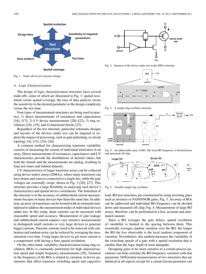
Fig. 1. Trade-offs in test structure design.
A. Logic Characterization
The design of logic characterization structures faces severaltrade-offs, some of which are illustrated in Fig. 1: spatial reso-lution versus spatial coverage, the ease of data analysis versusthe sensitivity to the desired parameter or the design complexityversus the test time.
Four types of measurement structures are being used in prac-tice: 1) direct measurements of resistances and capacitances[16], [17]; 2) I-V device measurements [20]–[22]; 3) ring os-cillators [18], [19]; and 4) functional blocks [23].
Regardless of the test structure, particular schematic designsand layouts of the devices under test can be targeted to ex-plore the impact of processing, such as gate patterning, or circuittopology [4], [15], [24]–[26].
A common method for characterizing transistor variabilityconsists of measuring the current of individual transistors in anarray. Direct measurements of resistances, capacitances and I-Vcharacteristics provide the distributions of desired values, butboth the stimuli and the measurements are analog, resulting inlong test times and limited datasets.
I-V characteristics of larger transistor arrays can be collectedusing device matrix arrays (DMAs), where many transistors canhave drains and sources connected to a single bus, while the gatevoltages are externally swept, shown in Fig. 2 [20], [27]. Thisstructure provides a large flexibility in analyzing each device’scharacteristics and spatial device correlations. The limitation ofthe structure is in the accuracy of subthreshold current measure-ments because of many devices that share the same line. In addi-tion, an array of transistors can be formed with its terminals mul-tiplexed to address the measurement nodes of individual devicesunder test. In this setup, drain currents can be measured withreasonable speed and accuracy. Measurement of gate leakageand subthreshold current requires very sensitive measurementsto distinguish small currents or very large devices to generatebigger currents. Parasitic currents need to be removed with cali-bration and random noise can be reduced by averaging the mea-surement over time. Using larger devices to get more current isa compromise with having a finer spatial resolution.
On the other hand, variability characterization using ring os-cillators (ROs) is commonly performed for high characteriza-tion speed and simple frequency measurements [28]. Variationin the frequency of the ROs is related to variation of device pa-rameters that affect transistor switching speed and capacitive
Fig. 2. Instance of the device under test in the DMA structure.
Fig. 3. A simple ring-oscillator structure.
Fig. 4. An addressable array of RO. The local RO frequency is divided downand measured off-chip.
Fig. 5. Variable-length ring oscillator.
load. RO test structures are constructed by using inverting gatessuch as inverters or NAND/NOR gates, Fig. 3. An array of ROscan be addressed and individual RO frequency can be divideddown and measured off-chip, Fig. 4. Measurement of large ROarrays, therefore, can be performed in a fast, accurate and auto-mated manner.
Since a RO averages the gate delays, spatial resolutionof variability is limited to the spacing between them. Thisessentially averages random variation over the RO: the longerthe RO the less observable is the local random component ofvariation. Nevertheless, this method measures the variability ofthe switching speeds of a gate with a spatial resolution that issmaller than the logic depth of most datapaths.
Designing gates to be more sensitive to a certain process pa-rameter can help correlate the RO frequency variation with thatparameter. Differential measurements of two structures that areidentical in all aspects except for a certain layout parameter can

NIKOLIC et al.: TECHNOLOGY VARIABILITY FROM A DESIGN PERSPECTIVE 1999
be used to isolate particular effects. This has been successfullyemployed to measure the impact of layout on transistor perfor-mance [15], [4] and in the measurement of the effects of NBTI[29]. It has been effective in isolating the effects of lithographyon the effective channel length, gate proximity, impact on den-sity and diffusion length on strain and STI-induced stress. Sim-ilarly, layouts can be sensitized to measure the impact of pro-cessing, such as defocus or misalignment [56].
Making electrical measurements of the same structureunder different environmental conditions can help to estimateprocess parameter variation. For example, by measuring thesubthreshold current and RO frequency at different tempera-tures, supply and back-bias voltages, the variation of the mainprocess parameters responsible for systematic variations canbe extracted. The same technique has been used to reveal theimpact of strain and proximity on device properties.
B. Characterization of Gate Delays
Ring oscillators efficiently characterize systematic varia-tions, but average out random, spatially uncorrelated effects.A simple concept of variable-length ring oscillators [30], canmeasure the delay of a pair of gates, and reduce the effect ofaveraging without compromising the speed and convenience ofthe method. This is accomplished by measuring the frequencydifferences between differently configured ring oscillators in[26].
Ring oscillators can be modified to allow for multiplexingin individual delay elements for delay characterization of indi-vidual gates [31].
The idea for characterizing individual delays through pathdifferences has been used for on-chip measurements of flip-flopsetup times and clock-to-output delays. Individual direct delaymeasurements have been performed for flip-flop setup andclock-output delays [32]. By placing appropriately configuredflip-flops into ring-oscillator configurations, variations in thesetup times and clock-to-output delays can be measured as well[33].
C. SRAM Characterization
The use of regular layouts has allowed aggressive scaling ofSRAM transistors compared to combinational logic. Simulta-neously, these highly scaled devices with design rules relaxedcompared to digital logic tend to exhibit higher sensitivities tosystematic effects in addition to increased random variation.Systematic effects that affect SRAM have been attributed totemperature nonuniformities during annealing, STI-inducedstress, and process-induced cell asymmetry [34]. Increasedvariability with technology scaling has a large negative impacton SRAM design. SRAM cells use the smallest transistorsavailable, and therefore are susceptible to largest amounts ofrandom variability, while the technology scaling enables inte-gration of twice as many cells in each new process generation.As a result, it is becoming necessary to satisfy the design wherethe functionality of the cell is guaranteed more than sevenstandard deviations away from the mean, while the standarddeviations in threshold voltages are increasing. Therefore,SRAM variability characterization over a wide range of processparameters presents a particular challenge. SRAM yield is
Fig. 6. Measurement macro for padded-out SRAM cells.
guaranteed through appropriate design margins against variousfailure modes. An array fails if any of its cells cannot be written,loses the value during the read, or cannot retain the value instandby.
Traditionally, SRAM design margins have been estimatedthrough SPICE and TCAD simulations for each of the failuremodes. However, as processes become increasingly com-plex and harder to control, along with the reduced devicegeometries, designers can no longer rely on model accuracyto fully capture the random effects in large cache memories.Recently, methods have been developed to characterize SRAMvariability by measuring dc read/write/retention margins insmall SRAM macros with wired-out storage nodes. In thesemacros SRAM is commonly characterized by measuring theI-V characteristics of its constituent transistors or by character-izing the static read stability or static writability of the SRAMcells [35]. This method requires the insertion of large switchnetworks to access all internal storage nodes without changingthe lithographic environment of the cells, Fig. 6. As a result,this approach is limited to smaller data volumes that may beunsuitable for failure analysis of large cache memory. Recentlarge-scale 3-D device simulations have demonstrated that evenjust random dopant fluctuations cause non-Gaussian distribu-tions of transistor threshold voltages in scaled technologies[36], making it difficult to estimate the behavior of cells inthe tail of the margin distributions. Conventional padded-outcell characterization techniques fail to characterize many ofthese effects due to insufficient spatial resolution and smalldatasets. Large-scale characterization techniques, involvingcharacterization of SRAM cells in situ within the array, providea better estimate of the impact of these systematic effects onSRAM performance. Thus, SRAM designers continue to relyon collecting distributions of bitline read currents [37], [37] and

2000 IEEE TRANSACTIONS ON CIRCUITS AND SYSTEMS—I: REGULAR PAPERS, VOL. 58, NO. 9, SEPTEMBER 2011
Fig. 7. Large-scale SRAM margin measurements [34].
Fig. 8. Dynamic SRAM characterization macro [42].
minimum operating voltage [37], [40] to gauge SRAMread stability and writeability in large functional SRAM arrays.
It has been recently demonstrated that read and write marginsof a large SRAM array can be measured by bitline current mea-surements using the setup in Fig. 7, in response to wordline,bitline, and supply voltage sweeps [34]. Distributions of readand write margins correlate well with the distributions of Vminduring read and write. Preserving the structure of the SRAMarray allows for collection of orders of magnitude more mea-sured variability data in the same chip area.
However, static margins provide only a partial variability pic-ture needed for robust SRAM design. By its definition, staticread margin is pessimistic—it assumes that the cell is under theread stress for an infinitely long time. Conversely, static writemargin is overly optimistic, as it allows infinite time for thecell to be written. In practice, wordlines are pulsed for a shortamount of time, during which the cells are written and read.There is a recent trend in assessing dynamic SRAM read/writemargins, for more accurate estimation of the necessary oper-ating voltages [41].
Fig. 9. SRAM RO for estimating write margins [43].
Dynamic behavior can be characterized by driving thewordlines with variable pulsewidths, Fig. 8. [42]. Shorter pulsewidths result in decreased read and increased write failure rates.This method of characterizing the dynamic SRAM behavioris fairly compact and could be even embedded in practicalarrays. Another method for characterizing the dynamic SRAMbehavior is through the use of ring oscillators [43], [44]. Atunable ring oscillator can be connected to the bitlines; its os-cillating frequency would vary with each cell selected throughthe WL and connected within the RO to assess variability incell currents. An example RO for characterizing write marginsis shown in Fig. 9 [43].
Repeated measurements using many of the presented struc-tures can be used for characterizing the time-dependent vari-ability of the SRAM characteristics. Simple repetitions of themeasurements under the same conditions expose the effects ofRTS noise. Measurements under increased supply voltage andelevated temperatures reveal the impact of BTI.
SRAM design in the presence of RTS noise therefore requiresaccurate characterization of the statistical distributions offluctuation, applied to a statistical model of SRAM failure, inorder to budget design margins appropriately. Enhanced char-acterization techniques have been proposed to speed up signifi-cantly the measurement of these statistical distributions [45].
IV. SYSTEMATIC AND RANDOM VARIATIONS IN LOGIC
The goal of logic variability studies is to improve the under-standing of the nature of variability, and to help classificationinto random and systematic components, including spatial andtemporal correlations.
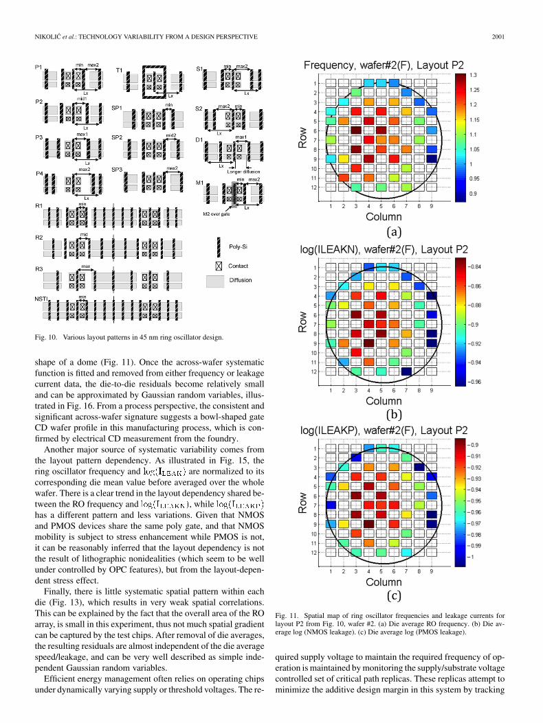
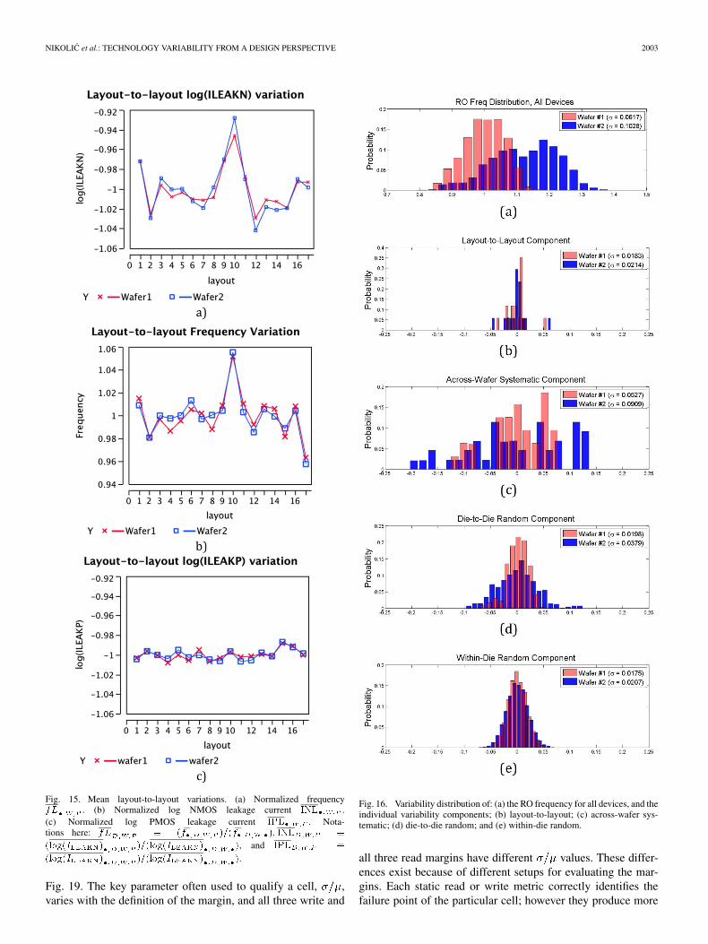
Many systematic variations in process can be exposed byvarying circuit layouts. A set of examples of varying inverterlayouts shown in Fig. 10, experiments with effects of gate prox-imity, and impact of STI or diffusion area on channel mobility.Frequency and leakage current measurements collected on ringthese oscillators from two 45 nm experimental wafers showedsignificant across wafer and systematic, layout-depended vari-ations [4]. Fig. 11 shows a spatial wafer map of the die av-erages of ring oscillator frequency (specifically for the layoutP2 from Fig. 10) and the log scale off-state leakage current forNMOS and PMOS transistors of same design as in the ring os-cillators. It has been found that the RO frequency and the logscale leakage currents are highly correlated to each other, as il-lustrated in Fig. 12, and thus can all be very well approximatedby a 2-D second-order polynomial function, with a reasonablequality of fit. The two experimental wafers, though subject toan intentional process split mainly in gate CD, share a similaracross-wafer spatial signature, shown in Fig. 14, which is the
NIKOLIC et al.: TECHNOLOGY VARIABILITY FROM A DESIGN PERSPECTIVE 2001
Fig. 10. Various layout patterns in 45 nm ring oscillator design.
shape of a dome (Fig. 11). Once the across-wafer systematicfunction is fitted and removed from either frequency or leakagecurrent data, the die-to-die residuals become relatively smalland can be approximated by Gaussian random variables, illus-trated in Fig. 16. From a process perspective, the consistent andsignificant across-wafer signature suggests a bowl-shaped gateCD wafer profile in this manufacturing process, which is con-firmed by electrical CD measurement from the foundry.
Another major source of systematic variability comes fromthe layout pattern dependency. As illustrated in Fig. 15, thering oscillator frequency and are normalized to itscorresponding die mean value before averaged over the wholewafer. There is a clear trend in the layout dependency shared be-tween the RO frequency and , whilehas a different pattern and less variations. Given that NMOSand PMOS devices share the same poly gate, and that NMOSmobility is subject to stress enhancement while PMOS is not,it can be reasonably inferred that the layout dependency is notthe result of lithographic nonidealities (which seem to be wellunder controlled by OPC features), but from the layout-depen-dent stress effect.
Finally, there is little systematic spatial pattern within eachdie (Fig. 13), which results in very weak spatial correlations.This can be explained by the fact that the overall area of the ROarray, is small in this experiment, thus not much spatial gradientcan be captured by the test chips. After removal of die averages,the resulting residuals are almost independent of the die averagespeed/leakage, and can be very well described as simple inde-pendent Gaussian random variables.
Efficient energy management often relies on operating chipsunder dynamically varying supply or threshold voltages. The re-
Fig. 11. Spatial map of ring oscillator frequencies and leakage currents forlayout P2 from Fig. 10, wafer #2. (a) Die average RO frequency. (b) Die av-erage log (NMOS leakage). (c) Die average log (PMOS leakage).
quired supply voltage to maintain the required frequency of op-eration is maintained by monitoring the supply/substrate voltagecontrolled set of critical path replicas. These replicas attempt tominimize the additive design margin in this system by tracking

2002 IEEE TRANSACTIONS ON CIRCUITS AND SYSTEMS—I: REGULAR PAPERS, VOL. 58, NO. 9, SEPTEMBER 2011
Fig. 12. Correlation among die average RO frequency, ����� � and����� �, for wafer #2 and layout P2 from Fig. 10.
Fig. 13. Within-die RO frequency map of layout pattern P2, averaged over alldies in wafer #2.
the most likely critical path for the particular supply voltage inthe given design corner. The mix of critical paths must be suffi-cient to identify the slowest path at each supply voltage, and isoften composed by mixing the NAND2 NAND3, NOR2 gates,inverters, interconnect, and pass-gates [55].
Measurements have shown that standard deviation of thedelay variability varies with the number of transistors in thetransistor stack, in addition to the overall transistor area shownin Fig. 17 [26].
One interesting direction in future designs is to allocate themargin for random variability dependent on the composition ofgates in the critical paths, to reflect this issue.
Fig. 14. Correlation between the same die location of the two experimentalwafers. (a) Die average RO frequency. (b) Die average ����� �. (c) Dieaverage ����� �.
V. VARIABILITY IN SRAM
Guaranteeing yield for a large array is a challenging statisticaloptimization problem, even with Gaussian distributions of eachtransistor’s parameters. This is because of the nonlinear depen-dence of the margins on the transistor parameters. Fig. 18 illus-trates the results obtained using characterization macros fromFigs. 6 and 7. All distributions are Gaussian near the center, butdeviate in the tails, as illustrated in normal probability plots in
NIKOLIC et al.: TECHNOLOGY VARIABILITY FROM A DESIGN PERSPECTIVE 2003
Fig. 15. Mean layout-to-layout variations. (a) Normalized frequency�� . (b) Normalized log NMOS leakage current ��� .(c) Normalized log PMOS leakage current ��� . Nota-tions here: �� � � �� ��� �� �� ��� �
���� � ������ � �, and ��� �
���� � ������ � �.
Fig. 19. The key parameter often used to qualify a cell, ,varies with the definition of the margin, and all three write and
Fig. 16. Variability distribution of: (a) the RO frequency for all devices, and theindividual variability components; (b) layout-to-layout; (c) across-wafer sys-tematic; (d) die-to-die random; and (e) within-die random.
all three read margins have different values. These differ-ences exist because of different setups for evaluating the mar-gins. Each static read or write metric correctly identifies thefailure point of the particular cell; however they produce more

2004 IEEE TRANSACTIONS ON CIRCUITS AND SYSTEMS—I: REGULAR PAPERS, VOL. 58, NO. 9, SEPTEMBER 2011
Fig. 17. Increase in standard deviation of variability normalized by the meanring oscillator frequency, as a function of supply voltage. Numbers indicate dif-ferent ring-oscillator layouts, with 2 NMOS (2N), 3 NMOS (3N) transistors,and 2 NMOS and 2 PMOS (2N2P) transistors in stack.
Fig. 18. Distributions of various static read and write metrics measured atlow voltages. (a) Write margins, measured on a padded-out macro (IW) andon an SRAM array (BWTV and WWTW). (b) Read margins, measured on apadded-out macro (RSNM) and on an SRAM array (SRRV and WRRV). Themetrics are defined in [34].
or less differing values of margins for stable cells, simply be-cause of different cell excitations.
The point of failure for any of the stability criteria canbe found by tracing the variables using the steepest gradientmethod [46], [47]. The method can be accelerated using statis-tical techniques such as importance sampling [48], [47], [49]and statistical blockade [50].
To improve the read stability or writability in SRAM, theaverage margin is increased by adjusting one of the terminal
Fig. 19. Illustration of deviation from normality for the three representativeSRAM read margins.
voltages. Lowering the column supply voltage or writingwith bitline voltages less than 0 V has been used to improvethe writability of the cell, meanwhile, lowering the wordlinevoltage has been demonstrated to improve the read stabilitywhile trading off writability.
While these techniques have been applied at the design time,the design margins can be minimized by tracking the system-atic variations in the process. Since the wordline voltage reduc-tion trades off the increased read margin for the reduced writemargin, the optimum between the two can be sensed by aver-aging a number of SRAM cells stressed for both read and write[47].
While all of the current SRAM yield enhancement tech-niques target systematic components of variability, there is littlework in attempting to estimate the tails of distributions. Onepotentially promising approach is through the use of “canary”cells—cells that are designed to fail before any of the cells inthe array [51].
Time-dependent degradation in transistor performance due toBTI is also a major concern in SRAM. In contrast to logic cir-cuits which typically face alternating input logic levels, SRAMtransistors face the worst BTI conditions when a cell stores aconstant value—a dc bias is applied to the transistors for a pro-longed period of time. The fact that BTI affects both NMOS andPMOS devices in high-k processes makes SRAM marginsetting more complex because degrades at differentrates depending on whether the original distributionwas read- or write-margin limited.
RTS noise is a significant concern in SRAM design involvinghighly scaled transistors, as its magnitude scales faster than theRDF-induced variations. However, experimental results indi-cate that while large RTS noise magnitude is present in SRAMtransistors, the additional margin needed to compensate for RTSis actually much smaller. This is due to the fact that when con-volving a long-tailed distribution (RTS) with a normal distribu-tion (RDF), the outliers in the long-tailed distribution have a lowprobability of being the most probable failure point in the design[45]. Furthermore, both theoretical and experimental analysessuggest that at least some components of RTS noise and BTIstem from the same traps, and therefore should be included inthe same margin [52].
Fig. 20(a) shows that there are no significant spatially corre-lated effects in SRAM NMOS pull-down currents, which willresult in random distribution of static noise margins. Similarly,there is no significant spatial correlation in the distribution ofthe magnitude of random telegraph noise, shown in Fig. 20(b).

NIKOLIC et al.: TECHNOLOGY VARIABILITY FROM A DESIGN PERSPECTIVE 2005
Fig. 20. Spatial distribution of variability in an SRAM array. (a) Mismatch inpull-down drain currents. (b) Random telegraph noise magnitude.
Fig. 21. Illustration of short and long logic paths.
VI. IMPACT ON DIGITAL LOGIC
Digital logic typically utilizes larger devices than SRAM,which results in lower random variation per gate and a reduc-tion in impact of some of the components of systematic vari-ability. Furthermore, long critical paths in digital logic natu-rally average random, spatially uncorrelated variations. As aresult, longer critical paths reduce the impact of random vari-ability; the of random variability roughly decreases with
, where the N is the number of gates in the path. Longestpaths in a circuit need to meet the setup time requirement forthe receiving flip-flop, which need to be margined appropriately,as illustrated in Fig. 21. Shortest paths need to be margined foravoiding the hold time violations. Hold margins are often dic-tated by the timing mismatches between individual gates and arenot reduced through averaging. Systematic and spatially corre-lated variations are not averaged and is independent of thelogic depth. The hold time margin is essentially dictated by themismatch in the delays of clock buffers and a Clk-Q path of theflip-flop, which is shown in Fig. 22.
Fig. 22. Illustration of delays that correspond to setup, hold times and clock-to-output delays in a typical flip-flop.
In a typical VLSI design process, satisfying design corners isdeemed necessary and assumed sufficient to validate a design.This approach typically regards all variations as D2D, with alldevices on a chip having identical process parameters. WID spa-tial correlations between the clock and data timing paths presentan opportunity for reduction in setup time margin. Measure-ments in earlier technology nodes revealed spatial correlationradii of approximately 1 mm [18], [19]. These correlations arecaused by systematic processing effects; however, they are notmodeled and therefore appear as random, with a certain degreeof spatial correlation [61]. These spatial correlations are of theorder of the size of a typical digital block, which makes manypaths inside a block partially correlated, allowing for some re-duction in margins. However, measurements in 45 nm tech-nology reveal negligible spatial correlations at the block level[4]. This is caused by: 1) improvements in processing technolo-gies; 2) reduced gate sizing, which increases true random vari-ability, potentially masking the spatially correlated component.It is believed, however, that the reticle-level spatial effects arestill present [7]. These effects can be used to establish timingcorrelations for interblock data and clock distributions in timinganalysis.
Spatial, processing-induced correlations are not the only onespresent in the chip. Layout-induced variations are common forall gates with the same topology or with the same neighborhood,and are therefore systematic. However, since many of the effectsare not modeled, they appear to the designer as random. Theycan be corrected by better processing, accounted for during cir-cuit extraction from the layout and acknowledged in the models,or can be treated statistically in the timing analysis.
Flip-flops are topologically the most complex cells in a stan-dard-cell library. Variability affects their clock-to-output delay,setup and hold times in a partially correlated way, since some ofthe transistors are shared between these timing paths, as illus-trated in Fig. 22. The variability of these gates is proportional tothe stack height, not unlike complex combinatorial gates. As aresult, flip-flops often limit minimum operating voltage of dig-ital logic [60].
Traditionally, correct functioning of digital logic is verifiedby using static timing analysis (STA), which checks if all timingpaths meet their setup and hold requirements. This is accom-plished by building a directed graph that corresponds to the ana-lyzed circuit, where vertices represent the gates and edges repre-sent the interconnect, each labeled with their respective delays.By using a breadth-first algorithm, a timing analysis tool goesthrough all the nodes of the graph and for each node computes
2006 IEEE TRANSACTIONS ON CIRCUITS AND SYSTEMS—I: REGULAR PAPERS, VOL. 58, NO. 9, SEPTEMBER 2011
the maximum of delays from all edges incurring in that node.Simple one time traversal of the graph finds the longest and theshortest path in the circuit. In traditional STA, which is incre-mental in nature, early and late signal arrivals depend only on thecircuit topology; however, to correctly account for variability alldelays have to have a lower and an upper bound. To account forvariability in STA, this verification has been performed in mul-tiple process corners. However, the closest point of failure doesnot necessarily correspond to one of the traditional corners; as aresult, the number of process corners for design verification hasbeen increasing.
Multicorner STA may introduce artificially large margins inthe design. When treating the signal delays as intervals in STAand performing timing analysis with the worst case delays (i.e.,taking the lower delay bound for the early signals and the upperdelay bound for the late signals) conventional STA cannot dis-tinguish the fact that two paths can have common or correlatedpart; the common part will be treated as having both, the lowerand upper delay bound at the same time. The common-path pes-simism removal (CPPR) technique and its generalization [58],[59], alleviate the pessimism of common or spatially correlatedpaths. For each critical path with a slack still bellow the crit-ical value, additional correlated path delay difference is applied.The delays are expressed as functions of parameters, explic-itly showing variations. For each corner, each parameter has ashared global value and an individual local value. One of themain drawbacks of the CPPR technique is its polynomial com-putational time.
An alternative approach for timing analysis is statisticalSTA (SSTA). In particular, block-based SSTA tries to recoverlinear run-time complexity, identification of a critical path andincremental nature of a traditional STA [57]. In SSTA, processparameters are considered to be random variables. A canonicalfirst-order delay model is employed for all timing quantities,consisting of the nominal delay value, and global and localprocess variations, multiplied by their respective sensitivities.When all delays are represented in the canonical form, graphcan be traversed in an STA fashion by using a breath-firstsearch. The graph traversal will result in the paths enumeratedin the order of critical probability. A spatial correlation factorcan be added to the canonical form as well.
Another way of accounting for systematic and random vari-ability is by adjusting the operating supply and frequency bymonitoring a replica of critical path delays [54]. To account fordependences in variability of different gate topologies on thesupply voltage, an appropriate mix of gates should compose theset of critical and near-critical path replicas [55]. In contrast, itis possible to monitor the timing violations on a set of actualcritical paths using shadow latches [62].
VII. CONCLUSION
Variability limits the lowest operating voltage for a tech-nology. This presents a challenge for continued scaling, whereone of the major scenarios relies on continued improvementsin energy efficiency of multicore processors through voltagescaling. To overcome voltage scaling barriers, variabilitycharacterization needs to be extended to enable compact, in
situ energy and performance monitoring of logic and memoryblocks. Continued improvement in design techniques, whichincorporate mitigation of the effects of variability, in additionto continuous performance monitoring would enable operationof high-volume products at near-threshold supplies.
ACKNOWLEDGMENT
The authors would like to thank the contributions of stu-dents, faculty and member companies of the Berkeley WirelessResearch Center. In particular, we are grateful to Prof. Tsu-JaeKing Liu, Prof, Prof. Andrew Neureuther, Dr. YasumasaTsukamoto, Dr. Andrew Carlson, Dr. Radu Zlatanovici,Changhwan Shin, Lynn Wang, Jason Tsai, Kenneth Duong, andLauren Jones.
REFERENCES
[1] K. A. Bowman, S. G. Duvall, and J. D. Meindl, “Impact of die-to-dieand within-die parameter fluctuations on the maximum clock frequencydistribution for gigascale integration,” IEEE J. Solid-State Circuits, vol.37, no. 2, pp. 183–190, Feb. 2002.
[2] J. W. Tschanz et al., “Adaptive body bias for reducing impacts ofdie-to-die and within-die parameter variations on microprocessorfrequency and leakage,” IEEE J. Solid-State Circuits, vol. 37, no. 11,pp. 1396–1402, Nov. 2002.
[3] K. Bernstein et al., “High-performance CMOS variability in the65-nm regime and beyond,” IBM J. Res. Develop., vol. 50, no. 4–5,pp. 433–449, Jul./Sep. 2006.
[4] L.-T. Pang, K. Qian, C. Spanos, and B. Nikoli, “Measurement and anal-ysis of variability in 45 nm strained-Si CMOS technology,” IEEE J.Solid-State Circuits, vol. 44, no. 8, pp. 2233–2244, Aug. 2009.
[5] D. Markovic, V. Stojanovic, B. Nikolic, M. A. Horowitz, and R. W.Brodersen, “Methods for true energy-performance optimization,” IEEEJ. Solid-State Circuits, vol. 39, no. 8, pp. 1282–1293, Aug. 2004.
[6] S. Nassif, “Delay variability: Sources, impacts and trends,” in IEEE Int.Solid-State Circuits Conf., Dig. Tech. Papers, San Francisco, CA, Feb.2000, pp. 368–369.
[7] K. Qian and C. J. Spanos, “A comprehensive model of process vari-ability for statistical timing optimization,” in Proc. SPIE Design forManufacturability through Design-Process Integration II, V. K. Singhand M. L. Rieger, Eds., 2008, vol. 6925, pp. 1G–1-11.
[8] A. B. Kahng and Y. C. Pati, “Subwavelength lithography and its poten-tial impact on design and EDA,” in Proc. Design Autom. Conf., NewOrleans, LA, Jun. 1999, pp. 799–804.
[9] P. Oldiges et al., “Modeling line edge roughness effects in sub 100nanometer gate length devices,” in Proc. Int. Conf. Simul. Semi-cond. Processes Devices (SISPAD), Seattle, WA, Sep. 6–8, 2000, pp.131–134.
[10] A. Asenov, S. Kaya, and J. H. Davies, “Intrinsic threshold voltage fluc-tuations in decanano MOSFETs due to local oxide thickness varia-tions,” IEEE Trans. Electron Devices, vol. 49, no. 1, pp. 112–119, Jan.2002.
[11] D. J. Frank, Y. Taur, M. Ieong, and H.-S. P. Wong, “Monte Carlomodeling of threshold variation due to dopant fluctuations,” in Proc.Symp. VLSI Circuits, Dig. Tech. Papers, Kyoto, Japan, Jun. 1999, pp.171–172.
[12] J. C. Lin, A. S. Oates, and C. H. Yu, “Time dependent ��� degra-dation of SRAM fabricated with high-k gate dielectrics,” in Proc. 45thAnnu. IEEE Int. Rel.. Phys. Symp., Phoenix, AZ, Apr. 15–19, 2007, pp.439–444.
[13] N. Tega et al., “Increasing threshold voltage variation due to randomtelegraph noise in FETs as gate lengths scale to 20 nm,” in Proc. Symp.VLSI Tech. Dig Tech. Papers, Kyoto, Japan, Jun. 2009, pp. 50–51.
[14] H. Onodera, “Variability: Modeling and its impact on design,” IEICETrans. Electron., vol. E89-C, no. 3, pp. 342–348, Mar. 2006.
[15] L.-T. Pang and B. Nikoli, “Measurements and analysis of process vari-ability in 90 nm CMOS,” IEEE J. Solid-State Circuits, vol. 44, no. 5,pp. 1655–1663, May 2009.
[16] M. Orshansky, L. Milor, and C. Hu, “Characterization of spatial in-trafield gate CD variability, its impact on circuit performance, and spa-tial mask-level correction,” IEEE Trans. Semicond. Manuf., vol. 17, no.1, pp. 2–11, Jan. 2004.

NIKOLIC et al.: TECHNOLOGY VARIABILITY FROM A DESIGN PERSPECTIVE 2007
[17] D. Sylvester, J. C. Chen, and C. Hu, “Investigation of interconnectcapacitance characterization using charge-based capacitance mea-surement (CBCM) technique and three-dimensional simulation,”IEEE J. Solid-State Circuits, vol. 33, no. 3, pp. 449–453, Mar.1998.
[18] K. Gonzalez-Valentin, “Extraction of variation sources due to layoutpractices,” M.S. thesis, Mass. Inst. Technol., Cambridge, MA, 2002.
[19] J. S. Panganiban, “A ring oscillator based variation test chip,” M.S.Thesis, Mass. Inst. Technol., Cambridge, MA, 2002.
[20] K. Agarwal et al., “A test structure for characterizing local device mis-matches,” in Proc. Symp. VLSI Circuits Dig. Tech. Papers, Honolulu,HI, Jun. 2006, pp. 67–68.
[21] L. T. Pang and B. Nikoli, “Impact of layout on 90 nm CMOS processparameter fluctuations,” in Proc. Symp. VLSI Circuits, Dig. Tech. Pa-pers, Honolulu, HI, Jun. 2006, pp. 84–85.
[22] V. Wang and K. L. Shepard, “On-chip transistor characterisation arraysfor variability analysis,” Electron. Lett., vol. 43, no. 15, pp. 806–807,July 19, 2007.
[23] N. Drego, A. Chandrakasan, and D. Boning, “All-digital circuits formeasurement of spatial variation in digital circuits,” IEEE J. Solid-StateCircuits, vol. 45, no. 3, pp. 640–651, Mar. 2010.
[24] B. Wan, J. Wang, G. Keskin, and L. T. Pileggi, “Ring oscillators forsingle process-parameter monitoring,” in Proc. IEEE Workshop TestStruct. Design Variability Characterization, San Jose, CA, Nov. 2008.
[25] L. T.-N. Wang, L.-T. Pang, A. R. Neureuther, and B. Nikolic, “Param-eter-specific electronic measurement and analysis of sources of vari-ation using ring oscillators,” in Proc. SPIE 7275, San Jose, CA, Feb.22–27, 2009, pp. 72750L–7275L-10.
[26] J.-H. Park, L.-T. Pang, K. Duong, and B. Nikoli, “Fixed- and variable-length ring oscillators for variability characterization in 45 nm CMOS,”in IEEE Custom Integr. Circuits Conf., San Jose, CA, Sep. 13–16, 2009,pp. 519–522.
[27] S. Ohkawa, M. Aoki, and H. Masuda, “Analysis and characterizationof device variations in an LSI chip using an integrated device matrixarray,” IEEE Trans. Semicond. Manuf., vol. 17, no. 2, pp. 155–165,May 2004.
[28] M. Bhushan, A. Gattiker, M. B. Ketchen, and K. K. Das, “Ring oscil-lators for CMOS process tuning and variability control,” IEEE Trans.Semicond. Manuf., vol. 19, no. 1, pp. 10–18, Feb. 2006.
[29] T. Kim, R. Persaud, and C. H. Kim, “Silicon odometer: An on-chipreliability monitor for measuring frequency degradation of digital cir-cuits,” IEEE J. Solid State Circuits, vol. 43, no. 4, pp. 874–880, Apr.2008.
[30] B. Zhou and A. Khouas, “Measurement of delay mismatch due toprocess variations by means of modified ring oscillators,” in Proc.2005 IEEE Int. Symp. Circuits Syst. (ISCAS), Kobe, Japan, May 2005,pp. 5246–5249.
[31] B. P. Das, B. Amrutur, H. S. Jamadagni, N. V. Arvind, and V.Visvanathan, “Within-die gate delay variability measurement usingre-configurable ring oscillator,” in Proc. IEEE Custom Integr. CircuitsConf., San Jose, CA, Sep. 2008, pp. 133–136.
[32] N. Nedovic, W. W. Walker, and V. G. Oklobdzija, “A test circuit formeasurement of clocked storage element characteristics,” IEEE J.Solid-State Circuits, vol. 39, no. 8, pp. 1294–1304, Aug. 2004.
[33] K. Duong, “Circuits for Measurement of Flip-Flop Performance Vari-ability,” M.S. Thesis, Univ. California, Berkeley, 2008.
[34] Z. Guo, A. Carlson, L.-T. Pang, K. Duong, T.-J. K. Liu, and B.Nikolic, “Large-scale SRAM variability characterization in 45 nmCMOS,” IEEE J. Solid-State Circuits, vol. 44, no. 11, pp. 3174–3192,Nov. 2009.
[35] A. Bhavnagarwala et al., “Fluctuation limits and scaling opportunitiesfor CMOS SRAM cells,” in IEEE Int. Electron Devices Meet. (IEDM)Tech. Dig., 2005, pp. 675–678.
[36] D. Reid, C. Millar, G. Roy, S. Roy, and A. Asenov, “Analysisof threshold voltage distribution due to random dopants: A 100000-sample 3-D simulation study,” IEEE Trans. Electron Devices, vol.56, no. 10, pp. 2255–2263, 2009.
[37] T. Fischer et al., “Analysis of read current and write trip voltage vari-ability from a 1-MB SRAM test structure,” IEEE Trans. Semicond.Manuf., vol. 21, no. 4, pp. 534–541, Nov. 2008.
[38] X. Deng, W. K. Loh, B. Pious, T. W. Houston, L. Liu, K. Bashar, andD. Corum, “Characterization of bit transistors in a functional SRAM,”in 2008 IEEE Symp. VLSI Circuits Dig. Tech. Papers, Honolulu, HI,Jun. 2008, pp. 44–45.
[39] M. Agostinelli et al., “Erratic fluctuations of SRAM cache VMIN at the90 nm process technology node,” in IEEE Int. Electron Devices Meet.(IEDM) Tech. Dig., 2005, pp. 655–658.
[40] M. Ball et al., “A screening methodology for � drift inSRAM arrays with applications to sub-65 nm nodes,” in IEEEInt. Electron Devices Meet. (IEDM 2006) Tech. Dig., pp. 1–4.
[41] D. Khalil et al., “Accurate estimation of SRAM dynamic stability,”IEEE Trans. Very Large Scale Integr. (VLSI) Syst., vol. 16, no.12, pp. 1639–1647, Dec. 2008.
[42] S. O. Toh, Z. Guo, and B. Nikolic, “Dynamic SRAM stabilitycharacterization in 45nm CMOS,” in Proc. Symp. VLSI Circuits,Dig. Tech Papers., Honolulu, HI, Jun. 16–18, 2010.
[43] G. D. Carpenter, “Pulsed Ring Oscillator Circuit for Storage CellRead Timing Evaluation,” U.S. Patent 7 409 305, Aug. 5, 2008,et al..
[44] J. Tsai, S. O. Toh, Z. Guo, L.-T. Pang, T.-J. King, and B.Nikolic, “SRAM variability characterization using tunable ringoscillators in 45 nm CMOS,” in Proc. IEEE Int. Solid-StateCircuits Conf. Dig. Tech. Papers., San Francisco, CA, Feb. 7–10,2010, pp. 354–355.
[45] S. O. Toh et al., “Impact of random telegraph signals on Vmin in45 nm SRAM,” in IEEE Int. Electron Devices Meeting (IEDM)Tech Dig., Dec. 2009, pp. 768–770.
[46] Y. Tsukamoto et al., “Worst-case analysis to obtain stable read/writeDC margin of high density 6T-SRAM-array with local Vth variability,”in Proc. IEEE Int. Conf. Comput.-Aided Design (ICCAD’05), SanJose, CA, pp. 398–405.
[47] A. E. Carlson, “Device and circuit techniques for reducing variationin nanoscale SRAM,” Ph.D. dissertation, Univ. California, Berkeley,2008.
[48] R. Kanj, R. Joshi, and S. Nassif, “Mixture importance samplingand its application to the analysis of SRAM designs in the presenceof rare failure events,” in Proc. Design Autom. Conf. (DAC), 2006,pp. 69–72.
[49] L. Dolecek, M. Qazi, D. Shah, and A. Chandrakasan, “Breaking thesimulation barrier: SRAM evaluation through norm minimization,”in Proc. IEEE Int. Conf. Comput.-Aided Design (ICCAD 2008),San Jose, CA, pp. 322–329.
[50] A. Singhee and R. Rutenbar, “Statistical blockade: A novel methodfor very fast Monte Carlo simulation of rare circuit events, andits application,” in Proc. DATE 2007, pp. 1–6.
[51] J. Wang and B. H. Calhoun, “Canary replica feedback for near-DRVstandby VDD scaling in a 90 nm SRAM,” in IEEE Custom Integr.Circuits Conf. (CICC), San Jose, CA, Sep. 2007.
[52] Y. Tsukamoto et al., “Analysis of the relationship between randomtelegraph signal and negative bias temperature instability,” in Proc.IEEE Int. Rel. Phys. Symp., Anaheim, CA, May 2–6, 2010.
[53] C. Visweswariah et al., “First-order incremental block-based statisticaltiming analysis,” IEEE Trans. Comput.-Aided Design Integr. CircuitsSyst., vol. 25, no. 10, pp. 2170–2180, Oct. 2006.
[54] T. D. Burd, T. Pering, A. Stratakos, and R. Brodersen, “A dynamicvoltage scaled microprocessor system,” in Proc. IEEE Int. Solid-StateCircuits Conf. (ISSCC) Dig. Tech. Papers, , Feb. 2000, pp. 294–295.
[55] A. Drake et al., “A distributed critical-path timing monitor fora 65 nm high-performance microprocessor,” in Proc. IEEE Int.Solid-State Circuits Conf. (ISSCC), San Francisco, CA, Feb. 2007,pp. 398–399.
[56] L. T.-N. Wang, N. Xu, S.-O. Toh, A. R. Neureuther, T.-J. K.Liu, and B. Nikolic, “Parameter-specific ring oscillator for processmonitoring at the 45 nm node,” in Proc. IEEE Custom Integr.Circuits Conf., CICC’10, San Jose, CA, Sep. 19–22, 2010.
[57] C. Visweswariah, K. Ravindran, K. Kalafala, S. G. Walker, andS. Narayan, “First-order incremental statistical timing analysis,”in Proc. Design Autom. Conf. (DAC), Jun. 2004.
[58] D. J. Hathaway, J. P. Alvarez, and K. P. Belkhale, “NetworkTiming Analysis Which Eliminates Timing Variations BetweenSignals Traversing a Common Circuit Path,” U.S. Patent 5 636372, Jun. 1997.
[59] K. Kalafala, P. Qi, D. J. Hathaway, A. J. Suess, and C. Visweswariah,“System and Method for Correlated Process Pessimism Removalfor Static Timing Analysis,” U.S. Patent 7 117 466, Oct. 2006.
[60] B. H. Calhoun and A. P. Chandrakasan, “Standby power reductionusing dynamic voltage scaling and canary flip-flop structures,” IEEEJ. Solid-State Circuits, vol. 39, no. 9, pp. 1504–1511, Sep. 2004.
[61] L. Cheng, P. Gupta, C. Spanos, K. Qian, and L. He, “Physicallyjustiable die-level modeling of spatial variation in view of systematicacross wafer variability,” in Proc. Design Autom. Conf., Jun. 2009.
[62] D. Ernst et al., “Razor: A low-power pipeline based on circuit-leveltiming speculation,” in Proc. 36th Annu. IEEE/ACM Int. Symp.Microarchit. (MICRO-36), 2003, pp. 7–18.

2008 IEEE TRANSACTIONS ON CIRCUITS AND SYSTEMS—I: REGULAR PAPERS, VOL. 58, NO. 9, SEPTEMBER 2011
Borivoje Nikolic (S’93-M’99-SM’05) received theDipl.Ing. and M.Sc. degrees in electrical engineeringfrom the University of Belgrade, Serbia, in 1992 and1994, respectively, and the Ph.D. degree from theUniversity of California at Davis in 1999.
He lectured electronics courses at the Universityof Belgrade from 1992 to 1996. He spent twoyears with Silicon Systems, Inc., Texas InstrumentsStorage Products Group, San Jose, CA, working ondisk-drive signal processing electronics. In 1999, hejoined the Department of Electrical Engineering and
Computer Sciences, University of California at Berkeley, where he is now aProfessor. He is coauthor of Digital Integrated Circuits: A Design Perspective(2nd ed., Prentice-Hall, 2003). His research activities include digital and analogintegrated circuit design and VLSI implementation of communications andsignal processing algorithms.
Dr. Nikolic received the NSF CAREER award in 2003, College of Engi-neering Best Doctoral Dissertation Prize and Anil K. Jain Prize for the BestDoctoral Dissertation in Electrical and Computer Engineering at University ofCalifornia at Davis in 1999, as well as the City of Belgrade Award for the BestDiploma Thesis in 1992. For work with his students and colleagues he receivedthe best paper awards at the ISSCC, Symposium on VLSI Circuits, ISLPED,and the International SOI Conference.
Ji-Hoon Park (S’06) received his B.S. and M.S. de-grees in electrical engineering from Seoul NationalUniversity, Korea, in 1998 and 2000, respectively. Heis currently working toward the Ph.D. degree at theUniversity of California at Berkeley.
From 2000 to 2005, he was with LG Electronics,Korea, where he worked on the design and verifica-tion of WCDMA base stations and GSM modems.His current research interests include the variabilitymeasurement and the design of multi-Gb/s wirelessreceivers.
Mr. Park was a recipient of Samsung Scholarship from 2005 to 2009.
Jaehwa Kwak received the B.S. and M.S. degreesin electrical engineering from Seoul National Univer-sity, Seoul, Korea in 2004 and 2006, respectively. Heis currently working toward the Ph.D. degree at theUniversity of California, Berkeley.
From 2004 to 2006, he was a Graduate StudentResearcher with the Integrated Systems DesignLaboratory, Seoul National University, where heworked on the ethernet switch architecture and thebandwidth provision of broadband access networks.In 2006, he joined GCT Research, Inc. (also known
as GCT Semiconductor, Inc.), Seoul, where he was a staff engineer in chargeof designing digital system architectures for the wireless networks. Since 2009,he has been with the Department of Electrical Engineering and ComputerSciences, University of California, Berkeley. His research interests are in theareas of low power process architectures and error detection techniques of thesynchronous digital systems.
Bastien Giraud received the M.S. degree fromInstitut Supérieur d’Electronique et du Numérique(ISEN), France, and Polytechnique Marseille,France, in electrical engineering in 2005 and thePh.D. degree from Ecole Nationale Supérieure desTélécommunications (ENST), Paris, France, in 2008.His Ph.D. thesis was realized in the laboratories ofInstitut Supérieur d’Electronique de Paris (ISEP) incooperation with CEA/Leti (France), and was partof a French multi-laboratories project funded by theANR (National Research Agency). It is based on IC
design about SRAM memory in Double Gate fully depleted silicon-on-insulatorsub-32 nm technology, in which in-depth studies of SRAM memory cells andsense amplifiers have been conducted..
In 2005, he interned at IMEC, Belgium, where he studied SRAM memoryarchitecture in Bulk-130n. In 2009, he spent one year as a postdoctoral re-searcher position at University of California, Berkeley, in the Berkeley WirelessResearch Center (BWRC) laboratories under the supervision of Prof. Nikolic.His research interests were in logic circuits and SRAM variability in Bulk 45nm. Since 2010, he has worked at CEA-Leti, Grenoble, France, as an IC designresearch engineer. His research interests include large range frequency digitaland SRAM circuit design, dynamic multi-Vt, Bulk IP porting in FD-SOI tech-nology.
Zheng Guo (S’03-M’09) received the B.S. degreein computer engineering from the University of Illi-nois at Urbana-Champaign in 2003 and the M.S. andPh.D. degrees in electrical engineering from the Uni-versity of California at Berkeley in 2005 and 2009, re-spectively. His Ph.D. research emphasis was on vari-ability characterization and robust design techniquesfor nanoscale SRAM.
He attended the University of California atBerkeley in the fall of 2003. There, he joined theBerkeley Wireless Research Center in 2004 as a
Graduate Student Researcher under the supervision of Professor BorivojeNikolic. Upon completion of his Ph.D. program, he joined Intel, Hillsboro, OR,in early 2010 as an SRAM technologist.
Dr. Guo was awarded the National Defense Science and Engineering Grad-uate (NDSEG) Fellowship in 2004. In 2005, he received the Best Paper Award atthe ACM/IEEE International Symposium of Low-Power Electronics. In 2009,his research work was recognized as a winner in the 46th DAC/ISSCC StudentDesign Contest.
Liang-Teck Pang (S’02-M’08) received theDipl.Ing. degree from Ecole Centrale de Paris,France, the M.Phil. degree from Cambridge Uni-versity, U.K., in 1997, and the Ph.D. degree in theDepartment of Electrical Engineering and ComputerSciences at the University of California, Berkeley,in 2008. His Ph.D. research involved the designof circuits to measure and characterize CMOSperformance variability due to fluctuations in themanufacturing process.
Between 1998 and 2002, he worked in the DSONational Labs in Singapore on VLSI implementation of signal processing algo-rithms and high performance microarchitecture and circuit design. In 2008, hejoined IBM T. J. Watson Research Center, Yorktown Heights, NY, as a researchstaff member. His research emphasis is on the effects of layout on CMOS per-formance, measurement of the spatial correlation of logic gates, and analysisof variability data. Currently in IBM, his research focus is in clocking of highperformance VLSI chips and 3-D chip design.
Seng Oon Toh received the B.S. degree (highesthonors) in computer engineering from the GeorgiaInstitute of Technology, Atlanta, in 2002, the M.S.degree in electrical engineering from the Universityof California at Berkeley in 2008. He is currentlyworking toward the Ph.D. degree at the Universityof California at Berkeley.
He is also currently working at Advanced MicroDevices, Sunnyvale, CA, on process technologydevelopment. His research emphasis is on power-per-formance optimization as well as robust design of
nanoscale SRAM, with emphasis on dynamic stability, RTS, and BTI.Mr. Toh was awarded an IBM Ph.D. fellowship in 2010 and won the DAC/
ISSCC student design contest in 2011.

NIKOLIC et al.: TECHNOLOGY VARIABILITY FROM A DESIGN PERSPECTIVE 2009
Ruzica Jevtic received the B.S. degree in electricalengineering from the University of Belgrade, Serbia,in 2004 and the Ph.D. degree in electrical engineeringwith European Ph.D. mention from the TechnicalUniversity of Madrid, Spain, in 2009. Her Ph.D.work was oriented towards CAD tools for high-levelmodeling, power estimation, measurements, andarchitecture design for high-speed computationalsystems in FPGAs.
She was a Predoctoral Visiting Researcher at theOFFIS Research Institute in Oldenburg, Germany, in
2007. She is currently working as a Postdoctoral Researcher at the Departmentof Electrical Engineering and Computer Sciences, University of California,Berkeley. Her current research interests are in energy efficient microprocessordesign.
Dr. Jevtic is a recipient of FP7 Marie Curie International Outgoing Fellow-ship.
Kun Qian (S’05) received the B.S. degree fromDepartment of Microelectronics, Peking University,Beijing, China, in 2005. He is currently workingtoward the Ph.D. degree in the Department ofElectrical Engineering and Computer Sciences, Uni-versity of California at Berkeley, under the guidanceof Prof. Costas J. Spanos.
Between 2003 and 2005 he did his undergradresearch with the Novel Devices Research Group ofInstitute of Microelectronics at PKU, which involvesmodeling of high-K dielectric based nonvolatile
memory devices. His Ph.D. research is focused on characterization, analysis,and modeling of integrated circuit manufacturing process and performancevariability, and the robust and accurate statistical extraction of compact modelparameters. He is also interested in general design for manufacturabilitytechniques.
Costas J. Spanos (F’00) received the Electrical Engi-neering Diploma degree from the National TechnicalUniversity of Athens, Greece, in 1980 and the M.S.and Ph.D. degrees in electrical and computer engi-neering from Carnegie Mellon University, Pittsburgh,PA, in 1981 and 1985, respectively.
From 1985 to 1988 he was with the advancedComputer-Aided Design Group of Digital Equip-ment Corporation, where he worked on the statisticalcharacterization, simulation, and diagnosis of VLSIprocesses. In 1988 he joined the Faculty at the de-
partment of Electrical Engineering and Computer Sciences of the University ofCalifornia at Berkeley, where he is now a Professor. He was the Director of theBerkeley Microfabrication Laboratory from 1994 to 2000, the Director of theElectronics Research Laboratory from 2004 to 2005, and the Associate Deanfor Research in the College of Engineering from 2004 to 2008. He is presentlythe Department Chair of EECS at UC Berkeley. His present research interestsinclude the application of statistical analysis in the design and fabricationof integrated circuits, and the development and deployment of novel sensorsand computer-aided techniques in semiconductor manufacturing. He is alsoworking towards the deployment of information technology and statistical datamining techniques for energy efficiency applications.
Prof. Spanos has served in the technical committees of numerous confer-ences and was the editor of the IEEE TRANSACTIONS ON SEMICONDUCTOR
MANUFACTURING from 1991 to 1994. In 2009 he was appointed in the AndrewS. Grove Distinguished Professorship in the Department of EECS.


![IEEE TRANSACTIONS ON CIRCUITS AND SYSTEMS …ssl.kaist.ac.kr/2007/data/journal/[2010_TCSVT]JooYoungKim.pdf · IEEE TRANSACTIONS ON CIRCUITS AND SYSTEMS FOR VIDEO TECHNOLOGY, VOL.](https://static.fdocuments.us/doc/165x107/5aa3c0047f8b9a84398ec6d7/ieee-transactions-on-circuits-and-systems-sslkaistackr2007datajournal2010tcsvt.jpg)