
18.10 GHz to 26.60 GHz Quadband VCO Data Sheet HMC8364
17
18.10 GHz to 26.60 GHz Quadband VCO Data Sheet HMC8364 Rev. A Document Feedback Information furnished by Analog Devices is believed to be accurate and reliable. However, no responsibility is assumed by Analog Devices for its use, nor for any infringements of patents or other rights of third parties that may result from its use. Specifications subject to change without notice. No license is granted by implication or otherwise under any patent or patent rights of Analog Devices. Trademarks and registered trademarks are the property of their respective owners. One Technology Way, P.O. Box 9106, Norwood, MA 02062-9106, U.S.A. Tel: 781.329.4700 ©2020 Analog Devices, Inc. All rights reserved. Technical Support www.analog.com FEATURES Set of 4 narrow-band VCOs with consistent sensitivity vs. frequency RF and tuning ports common to all 4 VCOs RF output operates from fundamental oscillators with no subharmonic oscillations Up to 4 dBm RF output power Power mute capability No external resonator required 40-lead, 6 mm × 6 mm LFCSP APPLICATIONS Electronic test and measurement Industrial and medical instrumentation Point to point and multipoint radios Aerospace and defense Wireless communication infrastructure FUNCTIONAL BLOCK DIAGRAM 1 NIC 2 GND 3 NIC 4 GND 5 RFOUT 6 GND 7 NIC 8 VCB 9 NIC 10 NIC 23 VC3 24 GND 25 VC2 26 GND 27 V TUNE 28 GND 29 VC1 30 NIC HMC8364 22 VC4 PACKAGE BASE 21 NIC GND 11 NIC 12 NIC 13 NIC 15 NIC 17 NIC 16 NIC 18 NIC 19 NIC 20 NIC 14 NIC 33 NIC 34 NIC 35 NIC 36 NIC 37 NIC 38 NIC 39 NIC 40 NIC 32 NIC 31 NIC 18.10GHz TO 20.10GHz 19.90GHz TO 22.30GHz 22.10GHz TO 24.10GHz 23.90GHz TO 26.60GHz 23681-001 Figure 1. GENERAL DESCRIPTION The HMC8364 is a gallium arsenide (GaAs), quadband, mono- lithic microwave integrated circuit (MMIC), voltage controlled oscillator (VCO) designed to offer wideband frequency capabilities without compromising phase noise performance. The device inte- grates four independent, narrow-band VCOs with overlapping frequency bands, operating at a fundamental frequency range of 18.10 GHz to 26.60 GHz. The consistent tuning sensitivity across all frequency bands simplifies the synthesizer loop filter design. The tuning port is common to all VCO cores for a simpler design of the phase-locked loop (PLL) feedback path. The HMC8364 also offers a low typical current consumption of 99 mA for power sensitive applications. The HMC8364 integrates resonators, negative resistance devices, and varactor diodes. The monolithic structure of the oscillator offers very low phase noise, optimal temperature stability, and is immune to vibration and process variation. The four VCOs are packaged in a single, 6 mm × 6 mm, surface-mount lead frame chip scale package (LFCSP), and require no external matching components. Combined with a high frequency, high performance PLL, the ADF41513, the HMC8364 offers a complete RF or microwave frequency generation solution.
Transcript of 18.10 GHz to 26.60 GHz Quadband VCO Data Sheet HMC8364

18.10 GHz to 26.60 GHz Quadband VCO Data Sheet HMC8364
Rev. A Document Feedback Information furnished by Analog Devices is believed to be accurate and reliable. However, no responsibility is assumed by Analog Devices for its use, nor for any infringements of patents or other rights of third parties that may result from its use. Specifications subject to change without notice. No license is granted by implication or otherwise under any patent or patent rights of Analog Devices. Trademarks and registered trademarks are the property of their respective owners.
One Technology Way, P.O. Box 9106, Norwood, MA 02062-9106, U.S.A. Tel: 781.329.4700 ©2020 Analog Devices, Inc. All rights reserved. Technical Support www.analog.com
FEATURES Set of 4 narrow-band VCOs with consistent sensitivity vs.
frequency RF and tuning ports common to all 4 VCOs RF output operates from fundamental oscillators with no
subharmonic oscillations Up to 4 dBm RF output power Power mute capability No external resonator required 40-lead, 6 mm × 6 mm LFCSP
APPLICATIONS Electronic test and measurement Industrial and medical instrumentation Point to point and multipoint radios Aerospace and defense Wireless communication infrastructure
FUNCTIONAL BLOCK DIAGRAM
1NIC
2GND
3NIC
4GND
5RFOUT
6GND
7NIC
8VCB
9NIC
10NIC
23 VC3
24 GND
25 VC2
26 GND
27 VTUNE
28 GND
29 VC1
30 NIC
HMC8364
22 VC4
PACKAGEBASE
21 NIC
GND
11NI
C12
NIC
13NI
C
15NI
C
17NI
C
16NI
C
18NI
C19
NIC
20NI
C
14NI
C
33NI
C
34NI
C
35NI
C
36NI
C
37NI
C
38NI
C
39NI
C
40NI
C
32NI
C
31NI
C
18.10GHz TO20.10GHz
19.90GHz TO22.30GHz
22.10GHz TO24.10GHz
23.90GHz TO26.60GHz
2368
1-00
1
Figure 1.
GENERAL DESCRIPTION The HMC8364 is a gallium arsenide (GaAs), quadband, mono-lithic microwave integrated circuit (MMIC), voltage controlled oscillator (VCO) designed to offer wideband frequency capabilities without compromising phase noise performance. The device inte-grates four independent, narrow-band VCOs with overlapping frequency bands, operating at a fundamental frequency range of 18.10 GHz to 26.60 GHz. The consistent tuning sensitivity across all frequency bands simplifies the synthesizer loop filter design.
The tuning port is common to all VCO cores for a simpler design of the phase-locked loop (PLL) feedback path. The HMC8364 also offers a low typical current consumption of 99 mA for power sensitive applications.
The HMC8364 integrates resonators, negative resistance devices, and varactor diodes. The monolithic structure of the oscillator offers very low phase noise, optimal temperature stability, and is immune to vibration and process variation.
The four VCOs are packaged in a single, 6 mm × 6 mm, surface-mount lead frame chip scale package (LFCSP), and require no external matching components.
Combined with a high frequency, high performance PLL, the ADF41513, the HMC8364 offers a complete RF or microwave frequency generation solution.
HMC8364 Data Sheet
Rev. A | Page 2 of 17
TABLE OF CONTENTS Features .............................................................................................. 1 Applications ...................................................................................... 1 Functional Block Diagram .............................................................. 1 General Description ......................................................................... 1 Revision History ............................................................................... 2 Specifications .................................................................................... 3 Absolute Maximum Ratings ........................................................... 5
Thermal Resistance ...................................................................... 5 Electrostatic Discharge (ESD) Ratings ...................................... 5 ESD Caution.................................................................................. 5
Pin Configuration and Function Descriptions ............................ 6
Interface Schematics .....................................................................6 Typical Performance Characteristics .............................................7
Band 1: 18.10 GHz to 20.10 GHz, VCC = 5 V .............................7 Band 2: 19.90 GHz to 22.30 GHz, VCC = 5 V .............................9 Band 3: 22.10 GHz to 24.10 GHz, VCC = 5 V .......................... 11 Band 4: 23.90 GHz to 26.60 GHz, VCC = 5 V .......................... 13
Theory of Operation ...................................................................... 15 Applications Information ............................................................. 16 Outline Dimensions ....................................................................... 17
Ordering Guide .......................................................................... 17
REVISION HISTORY 9/2020—Revision A: Initial Version
Data Sheet HMC8364
Rev. A | Page 3 of 17
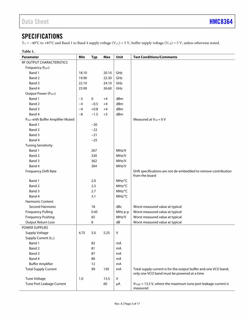
SPECIFICATIONS TA = −40°C to +85°C and Band 1 to Band 4 supply voltage (VCC) = 5 V, buffer supply voltage (VCB) = 5 V, unless otherwise noted.
Table 1. Parameter Min Typ Max Unit Test Conditions/Comments RF OUTPUT CHARACTERISTICS
Frequency (fOUT) Band 1 18.10 20.10 GHz Band 2 19.90 22.30 GHz Band 3 22.10 24.10 GHz Band 4 23.90 26.60 GHz
Output Power (POUT) Band 1 −3 0 +4 dBm Band 2 −4 −0.5 +4 dBm Band 3 −4 +0.8 +4 dBm Band 4 −8 −1.5 +3 dBm
POUT with Buffer Amplifier Muted Measured at VCB = 0 V Band 1 −20 Band 2 −22 Band 3 −21 Band 4 −25
Tuning Sensitivity Band 1 267 MHz/V Band 2 330 MHz/V Band 3 362 MHz/V Band 4 364 MHz/V
Frequency Drift Rate Drift specifications are not de-embedded to remove contribution from the board
Band 1 2.0 MHz/°C Band 2 2.3 MHz/°C Band 3 2.7 MHz/°C Band 4 3.1 MHz/°C
Harmonic Content Second Harmonic 18 dBc Worst measured value at typical
Frequency Pulling 0.45 MHz p-p Worst measured value at typical Frequency Pushing 65 MHz/V Worst measured value at typical Output Return Loss 8 dB Worst measured value at typical
POWER SUPPLIES Supply Voltage 4.75 5.0 5.25 V Supply Current (ICC)
Band 1 83 mA Band 2 81 mA Band 3 87 mA Band 4 80 mA Buffer Amplifier 12 mA
Total Supply Current 99 130 mA Total supply current is for the output buffer and one VCO band; only one VCO band must be powered at a time
Tune Voltage 1.0 13.5 V Tune Port Leakage Current 60 μA VTUNE = 13.5 V, where the maximum tune port leakage current is
measured

HMC8364 Data Sheet
Rev. A | Page 4 of 17
Parameter Min Typ Max Unit Test Conditions/Comments SINGLE SIDEBAND PHASE NOISE
Band 1 10 kHz −66 dBc/Hz 100 kHz −95 dBc/Hz 1 MHz −122 dBc/Hz
Band 2 10 kHz −65 dBc/Hz 100 kHz −92 dBc/Hz 1 MHz −120 dBc/Hz
Band 3 10 kHz −62 dBc/Hz 100 kHz −91 dBc/Hz 1 MHz −118 dBc/Hz
Band 4 10 kHz −62 dBc/Hz 100 kHz −89 dBc/Hz 1 MHz −118 dBc/Hz
Data Sheet HMC8364
Rev. A | Page 5 of 17
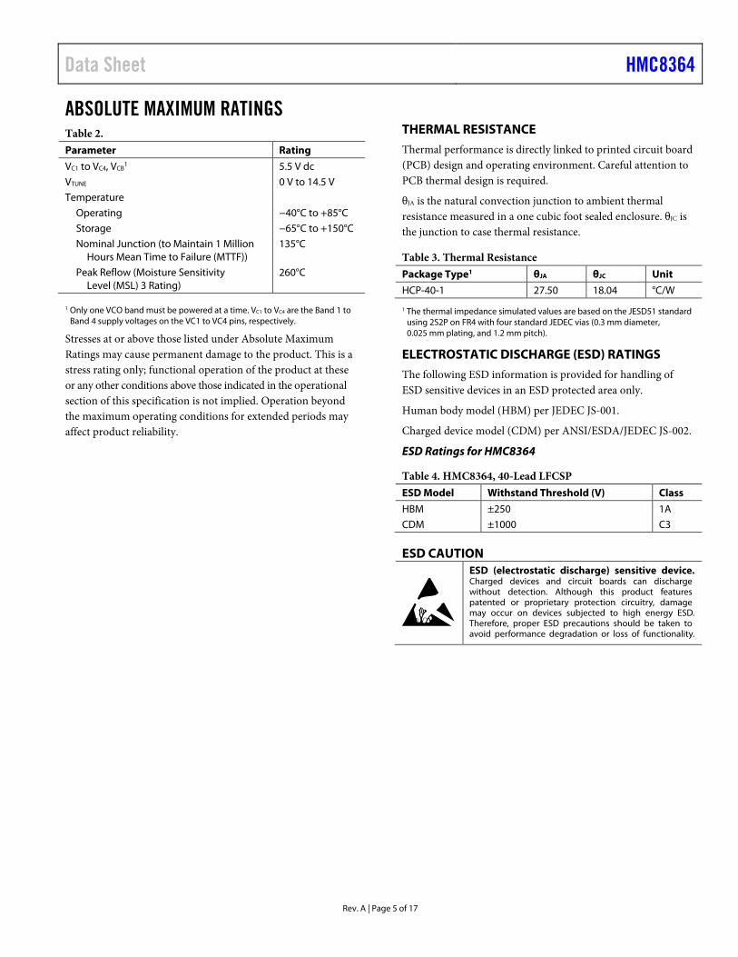
ABSOLUTE MAXIMUM RATINGS Table 2. Parameter Rating VC1 to VC4, VCB
1 5.5 V dc VTUNE 0 V to 14.5 V Temperature
Operating −40°C to +85°C Storage −65°C to +150°C Nominal Junction (to Maintain 1 Million
Hours Mean Time to Failure (MTTF)) 135°C
Peak Reflow (Moisture Sensitivity Level (MSL) 3 Rating)
260°C
1 Only one VCO band must be powered at a time. VC1 to VC4 are the Band 1 to Band 4 supply voltages on the VC1 to VC4 pins, respectively.
Stresses at or above those listed under Absolute Maximum Ratings may cause permanent damage to the product. This is a stress rating only; functional operation of the product at these or any other conditions above those indicated in the operational section of this specification is not implied. Operation beyond the maximum operating conditions for extended periods may affect product reliability.
THERMAL RESISTANCE Thermal performance is directly linked to printed circuit board (PCB) design and operating environment. Careful attention to PCB thermal design is required.
θJA is the natural convection junction to ambient thermal resistance measured in a one cubic foot sealed enclosure. θJC is the junction to case thermal resistance.
Table 3. Thermal Resistance Package Type1 θJA θJC Unit HCP-40-1 27.50 18.04 °C/W
1 The thermal impedance simulated values are based on the JESD51 standard using 2S2P on FR4 with four standard JEDEC vias (0.3 mm diameter, 0.025 mm plating, and 1.2 mm pitch).
ELECTROSTATIC DISCHARGE (ESD) RATINGS The following ESD information is provided for handling of ESD sensitive devices in an ESD protected area only.
Human body model (HBM) per JEDEC JS-001.
Charged device model (CDM) per ANSI/ESDA/JEDEC JS-002.
ESD Ratings for HMC8364
Table 4. HMC8364, 40-Lead LFCSP ESD Model Withstand Threshold (V) Class HBM ±250 1A CDM ±1000 C3
ESD CAUTION
HMC8364 Data Sheet
Rev. A | Page 6 of 17
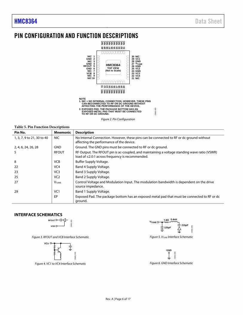
PIN CONFIGURATION AND FUNCTION DESCRIPTIONS
NOTE1. NIC = NO INTERNAL CONNECTION. HOWEVER, THESE PINS CAN BECONNECTED TO RF OR DC GROUND WITHOUT
AFFECTING THE PERFORMANCE OF THE DEVICE.2. EXPOSED PAD. THE PACKAGE BOTTOM HAS AN EXPOSED METAL PAD THAT MUST BE CONNECTED
TO RF OR DC GROUND.
1NIC2GND3NIC4GND5RFOUT6GND7NIC8VCB9NIC
10NIC
23 VC324 GND25 VC226 GND27 VTUNE28 GND29 VC130 NIC
22 VC421 NIC
11NI
C12
NIC
13NI
C
15NI
C
17NI
C16
NIC
18NI
C19
NIC
20NI
C
14NI
C
33NI
C34
NIC
35NI
C36
NIC
37NI
C38
NIC
39NI
C40
NIC
32NI
C31
NIC
HMC8364TOP VIEW
(Not to Scale)
2368
1-00
2
Figure 2. Pin Configuration
Table 5. Pin Function Descriptions Pin No. Mnemonic Description 1, 3, 7, 9 to 21, 30 to 40 NIC No Internal Connection. However, these pins can be connected to RF or dc ground without
affecting the performance of the device. 2, 4, 6, 24, 26, 28 GND Ground. The GND pins must be connected to RF or dc ground. 5 RFOUT RF Output. The RFOUT pin is ac-coupled, and maintaining a voltage standing wave ratio (VSWR)
load of ≤2.0:1 across frequency is recommended. 8 VCB Buffer Supply Voltage. 22 VC4 Band 4 Supply Voltage. 23 VC3 Band 3 Supply Voltage. 25 VC2 Band 2 Supply Voltage. 27 VTUNE Control Voltage and Modulation Input. The modulation bandwidth is dependent on the drive
source impedance. 29 VC1 Band 1 Supply Voltage. EP Exposed Pad. The package bottom has an exposed metal pad that must be connected to RF or dc
ground.
INTERFACE SCHEMATICS RFOUT
VCB 2368
1-00
3
Figure 3. RFOUT and VCB Interface Schematic
VCx
2368
1-00
4
Figure 4. VC1 to VC4 Interface Schematic
VTUNE
125pF
1.6Ω 0.4nH
215pF
2368
1-00
5
Figure 5. VTUNE Interface Schematic
GND
2368
1-00
6
Figure 6. GND Interface Schematic

Data Sheet HMC8364
Rev. A | Page 7 of 17
TYPICAL PERFORMANCE CHARACTERISTICS BAND 1: 18.10 GHz TO 20.10 GHz, VCC = 5 V
0 1 2 3 4 5 6 7 8 9 10 11 12 13 1415
16
17
18
19
20
21
22
OU
TP
UT
FR
EQ
UE
NC
Y (
GH
z)
TUNING VOLTAGE (V dc)
TA = –40°CTA = +25°CTA = +85°C
23681-007
Figure 7. Output Frequency vs. Tuning Voltage for Various Temperatures
0
200
400
600
800
1000
1200
1400
1600
1800
2000
2200
0 1 2 3 4 5 6 7 8 9 10 11 12 13 14
TU
NIN
G S
EN
SIT
IVIT
Y (
MH
z/V
)
TUNING VOLTAGE (V dc)
TA = –40°CTA = +25°CTA = +85°C
23681-009
Figure 8. Tuning Sensitivity vs. Tuning Voltage for Various Temperatures
–130
–125
–120
–115
–110
–105
–100
–95
–90
–85
–80
–75
–70
–65
–60
–55
–50
0 1 2 3 4 5 6 7 8 9 10 11 12 13 14
SIN
GL
E S
IDE
BA
ND
PH
AS
E N
OIS
E (
dB
c/H
z)
TUNING VOLTAGE (V dc)
–40°C, 10kHz+25°C, 10kHz+85°C, 10kHz
–40°C, 100kHz+25°C, 100kHz+85°C, 100kHz
–40°C, 1MHz+25°C, 1MHz+85°C, 1MHz
23681-011
Figure 9. Single Sideband Phase Noise vs. Tuning Voltage for Various Temperatures and Frequencies
–5
–4
–3
–2
–1
0
1
2
3
4
5
0 1 2 3 4 5 6 7 8 9 10 11 12 13 14
OU
TP
UT
PO
WE
R (
dB
m)
TUNING VOLTAGE (V dc)
TA = –40°CTA = +25°CTA = +85°C
23681-008
Figure 10. Output Power vs. Tuning Voltage for Various Temperatures
50
55
60
65
70
75
80
85
90
95
100
105
110
115
120
125
130
SU
PP
LY C
UR
RE
NT
(m
A)
TUNING VOLTAGE (V dc)
TA = –40°CTA = +25°CTA = +85°C
0 1 2 3 4 5 6 7 8 9 10 11 12 13 14
23681-010
Figure 11. Supply Current vs. Tuning Voltage for Various Temperatures
–170
–160
–150
–140
–130–120
–110
–100
–90–80
–70
–60
–50
–40–30
–20
–10
0
100 1k 10k 100k 1M 10M 40M
SIN
GL
E S
IDE
BA
ND
PH
AS
E N
OIS
E (
dB
c/H
z)
OFFSET FREQUENCY (Hz)
TA = –40°CTA = +25°CTA = +85°C
23681-012
Figure 12. Single Sideband Phase Noise vs. Offset Frequency for Various Temperatures at VTUNE = 5 V

HMC8364 Data Sheet
Rev. A | Page 8 of 17
–45
–40
–35
–30
–25
–20
–15
–10
–5
0
0 1 2 3 4 5 6 7 8 9 10 11 12 13 14
SECO
ND H
ARM
ONI
C (d
Bc)
TUNING VOLTAGE (V dc)
TA = –40°CTA = +25°CTA = +85°C
2368
1-11
3
Figure 13. Second Harmonic vs. Tuning Voltage for Various Temperatures
–30
–25
–20
–15
–10
–5
0
5
0 1 2 3 4 5 6 7 8 9 10 11 12 13 14
OUT
PUT
POW
ER (d
Bm)
TA = –40°CTA = +25°CTA = +85°C
TUNING VOLTAGE (V dc) 2368
1-11
4
Figure 14. Output Power vs. Tuning Voltage at VCB = 0 V for Various
Temperatures
2368
1-11
5–40
–35
–30
–25
–20
–15
–10
–5
0
5
10
RETU
RN L
OSS
(dB)
FREQUENCY (GHz)0 5 10 15 20 25 30 35 40 45 50
Figure 15. Return Loss vs. Frequency at VTUNE = 6 V

Data Sheet HMC8364
Rev. A | Page 9 of 17
BAND 2: 19.90 GHz TO 22.30 GHz, VCC = 5 V
17
18
19
20
21
22
23
24
0 1 2 3 4 5 6 7 8 9 10 11 12 13 14
OU
TP
UT
FR
EQ
UE
NC
Y (
GH
z)
TUNING VOLTAGE (V dc)
TA = –40°CTA = +25°CTA = +85°C
23681-013
Figure 16. Output Frequency vs. Tuning Voltage for Various Temperatures
0
200
400
600
800
1000
1200
1400
1600
1800
2000
2200
2400
TU
NIN
G S
EN
SIT
IVIT
Y (
MH
z/V
)
TUNING VOLTAGE (V dc)
TA = –40°CTA = +25°CTA = +85°C
0 1 2 3 4 5 6 7 8 9 10 11 12 13 14
23681-015
Figure 17. Tuning Sensitivity vs. Tuning Voltage for Various Temperatures
–125
–120
–115
–110
–105
–100
–95
–90
–85
–80
–75
–70
–65
–60
–55
–50
0 1 2 3 4 5 6 7 8 9 10 11 12 13 14
SIN
GL
E S
IDE
BA
ND
PH
AS
E N
OIS
E (
dB
c/H
z)
TUNING VOLTAGE (V dc)
–40°C, 10kHz+25°C, 10kHz+85°C, 10kHz
–40°C, 100kHz+25°C, 100kHz+85°C, 100kHz
–40°C, 1MHz+25°C, 1MHz+85°C, 1MHz
23681-017
Figure 18. Single Sideband Phase Noise vs. Tuning Voltage for Various Temperatures and Frequencies
–5
–4
–3
–2
–1
0
1
2
3
4
5
0 1 2 3 4 5 6 7 8 9 10 11 12 13 14
OU
TP
UT
PO
WE
R (
dB
m)
TUNING VOLTAGE (V dc)
TA = –40°CTA = +25°CTA = +85°C
23681-014
Figure 19. Ouput Power vs. Tuning Voltage for Various Temperatures
0 1 2 3 4 5 6 7 8 9 10 11 12 13 1450
55
60
65
70
75
80
85
90
95
100
105
110
115
120
125
130
SU
PP
LY C
UR
RE
NT
(m
A)
TUNING VOLTAGE (V dc)
TA = –40°CTA = +25°CTA = +85°C
23681-016
Figure 20. Supply Current vs. Tuning Voltage for Various Temperatures
–170
–160
–150
–140
–130–120
–110
–100
–90–80
–70
–60
–50
–40–30
–20
–10
0
100 1k 10k 100k 1M 10M
SIN
GL
E S
IDE
BA
ND
PH
AS
E N
OIS
E (
dB
c/H
z)
OFFSET FREQUENCY (Hz)
TA = –40°CTA = +25°CTA = +85°C
40M
23681-018
Figure 21. Single Sideband Phase Noise vs. Offset Frequency for Various Temperatures at VTUNE = 5 V

HMC8364 Data Sheet
Rev. A | Page 10 of 17
–50
–45
–40
–35
–30
–25
–20
–15
–10
–5
0
0 1 2 3 4 5 6 7 8 9 10 11 12 13 14
SECO
ND H
ARM
ONI
C (d
Bc)
TUNING VOLTAGE (V dc)
TA = –40°CTA = +25°CTA = +85°C
2368
1-12
2
Figure 22. Second Harmonic vs. Tuning Voltage for Various Temperatures
–30
–25
–20
–15
–10
–5
0
0 1 2 3 4 5 6 7 8 9 10 11 12 13 14
OUT
PUT
POW
ER (d
Bm)
TUNING VOLTAGE (V dc)
TA = –40°CTA = +25°CTA = +85°C
2368
1-12
3
Figure 23. Output Power vs. Tuning Voltage at VCB = 0 V for Various
Temperatures
2368
1-12
4
RETU
RN L
OSS
(dB)
FREQUENCY (GHz)0 5 10 15 20 25 30 35 40 45 50
10
5
0
–5
–10
–15
–20
–25
–30
–35
–40
Figure 24. Return Loss vs. Frequency at VTUNE = 6 V

Data Sheet HMC8364
Rev. A | Page 11 of 17
BAND 3: 22.10 GHz TO 24.10 GHz, VCC = 5 V
18
19
20
21
22
23
24
25
26
0 1 2 3 4 5 6 7 8 9 10 11 12 13 14
OU
TP
UT
FR
EQ
UE
NC
Y (
GH
z)
TUNING VOLTAGE (V dc)
TA = –40°CTA = +25°CTA = +85°C
23681-019
Figure 25. Output Frequency vs. Tuning Voltage for Various Temperatures
0 1 2 3 4 5 6 7 8 9 10 11 12 13 14
TU
NIN
G S
EN
SIT
IVIT
Y (
MH
z/V
)
TUNING VOLTAGE (V dc)
TA = –40°CTA = +25°CTA = +85°C
23681-021
Figure 26. Tuning Sensitivity vs. Tuning Voltage for Various Temperatures
–125
–120
–115
–110
–105
–100
–95
–90
–85
–80
–75
–70
–65
–60
–55
–50
0 1 2 3 4 5 6 7 8 9 10 11 12 13 14
SIN
GL
E S
IDE
BA
ND
PH
AS
E N
OIS
E (
dB
c/H
z)
TUNING VOLTAGE (V dc)
–40°C, 10kHz+25°C, 10kHz+85°C, 10kHz
–40°C, 100kHz+25°C, 100kHz+85°C, 100kHz
–40°C, 1MHz+25°C, 1MHz+85°C, 1MHz
23681-023
Figure 27. Single Sideband Phase Noise vs. Tuning Voltage for Various Temperatures and Frequencies
–5
–4
–3
–2
–1
0
1
2
3
4
5
0 1 2 3 4 5 6 7 8 9 10 11 12 13 14
OU
TP
UT
PO
WE
R (
dB
m)
TUNING VOLTAGE (V dc)
TA = –40°CTA = +25°CTA = +85°C
23681-020
Figure 28. Output Power vs. Tuning Voltage for Various Temperatures
50
55
60
65
70
75
80
85
90
95
100
105
110
115
120
125
130
SU
PP
LY C
UR
RE
NT
(m
A)
TUNING VOLTAGE (V dc)
TA = –40°CTA = +25°CTA = +85°C
0 1 2 3 4 5 6 7 8 9 10 11 12 13 14
23681-022
Figure 29. Supply Current vs. Tuning Voltage for Various Temperatures
100 1k 10k 100k 1M 10M
SIN
GL
E S
IDE
BA
ND
PH
AS
E N
OIS
E (
dB
c/H
z)
OFFSET FREQUENCY (Hz)
–180–170–160–150–140–130–120–110–100–90–80–70–60–50–40–30–20–10
0TA = –40°CTA = +25°CTA = +85°C
40M
23681-024
Figure 30. Single Sideband Phase Noise vs. Offset Frequency for Various Temperatures at VTUNE = 5 V

HMC8364 Data Sheet
Rev. A | Page 12 of 17
–50
–45
–40
–35
–30
–25
–20
–15
–10
–5
0
0 1 2 3 4 5 6 7 8 9 10 11 12 13 14
SECO
ND H
ARM
ONI
C (d
Bc)
TUNING VOLTAGE (V dc)
TA = –40°CTA = +25°CTA = +85°C
2368
1-13
1
Figure 31. Second Harmonic vs. Tuning Voltage for Various Temperatures
–30
–25
–20
–15
–10
–5
0
5
0 1 2 3 4 5 6 7 8 9 10 11 12 13 14
OUT
PUT
POW
ER (d
Bm)
TUNING VOLTAGE (V dc)
TA = –40°CTA = +25°CTA = +85°C
2368
1-13
2
Figure 32. Output Power vs. Tuning Voltage at VCB = 0 V for Various
Temperatures
2368
1-13
3–50
–40
–30
–20
–10
0
10
RETU
RN L
OSS
(dB)
FREQUENCY (GHz)0 5 10 15 20 25 30 35 40 45 50
Figure 33. Return Loss vs. Frequency at VTUNE = 6 V
Data Sheet HMC8364
Rev. A | Page 13 of 17
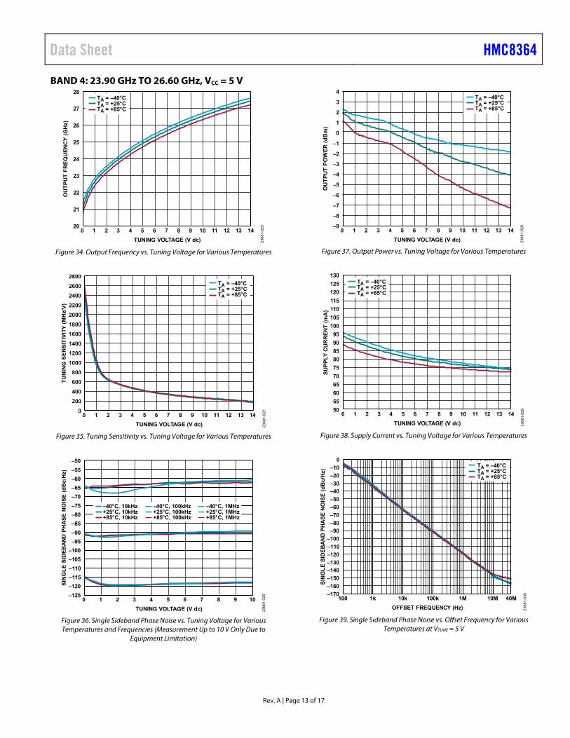
BAND 4: 23.90 GHz TO 26.60 GHz, VCC = 5 V
20
21
22
23
24
25
26
27
28
0 1 2 3 4 5 6 7 8 9 10 11 12 13 14
TUNING VOLTAGE (V dc)
TA = –40°CTA = +25°CTA = +85°C
OU
TP
UT
FR
EQ
UE
NC
Y (
GH
z)
23681-025
Figure 34. Output Frequency vs. Tuning Voltage for Various Temperatures
0 1 2 3 4 5 6 7 8 9 10 11 12 13 14
TU
NIN
G S
EN
SIT
IVIT
Y (
MH
z/V
)
TUNING VOLTAGE (V dc)
TA = –40°CTA = +25°CTA = +85°C
23681-027
Figure 35. Tuning Sensitivity vs. Tuning Voltage for Various Temperatures
–125
–120
–115
–110
–105
–100
–95
–90
–85
–80
–75
–70
–65
–60
–55
–50
0 1 2 3 4 5 6 7 8 9 10
SIN
GL
E S
IDE
BA
ND
PH
AS
E N
OIS
E (
dB
c/H
z)
TUNING VOLTAGE (V dc)
–40°C, 10kHz+25°C, 10kHz+85°C, 10kHz
–40°C, 100kHz+25°C, 100kHz+85°C, 100kHz
–40°C, 1MHz+25°C, 1MHz+85°C, 1MHz
23681-029
Figure 36. Single Sideband Phase Noise vs. Tuning Voltage for Various Temperatures and Frequencies (Measurement Up to 10 V Only Due to
Equipment Limitation)
–9
–8
–7
–6
–5
–4
–3
–2
–1
0
1
2
3
4
0 1 2 3 4 5 6 7 8 9 10 11 12 13 14
OU
TP
UT
PO
WE
R (
dB
m)
TUNING VOLTAGE (V dc)
TA = –40°CTA = +25°CTA = +85°C
23681-026
Figure 37. Output Power vs. Tuning Voltage for Various Temperatures
0 1 2 3 4 5 6 7 8 9 10 11 12 13 1450
55
60
65
70
75
80
85
90
95
100
105
110
115
120
125
130
SU
PP
LY C
UR
RE
NT
(m
A)
TUNING VOLTAGE (V dc)
TA = –40°CTA = +25°CTA = +85°C
23681-028
Figure 38. Supply Current vs. Tuning Voltage for Various Temperatures
100 1k 10k 100k 1M 10M
SIN
GL
E S
IDE
BA
ND
PH
AS
E N
OIS
E (
dB
c/H
z)
OFFSET FREQUENCY (Hz)
–170
–160
–150
–140–130
–120
–110
–100
–90–80
–70
–60
–50
–40–30
–20
–10
0TA = –40°CTA = +25°CTA = +85°C
40M
23681-030
Figure 39. Single Sideband Phase Noise vs. Offset Frequency for Various Temperatures at VTUNE = 5 V

HMC8364 Data Sheet
Rev. A | Page 14 of 17
–50
–45
–40
–35
–30
–25
–20
–15
–10
–5
0
0 0.5 1.0 1.5 2.0 2.5 3.0 3.5 4.0 4.5 5.0 5.5 6.0 6.5
SECO
ND H
ARM
ONI
C (d
Bc)
TUNING VOLTAGE (V dc)
TA = –40°CTA = +25°CTA = +85°C
2368
1-14
0
Figure 40. Second Harmonic vs. Tuning Voltage for Various Temperatures
(Measurement Up to 6.5 V Only Due to Equipment Limitation)
–35
–30
–25
–20
–15
–10
–5
0
5
0 1 2 3 4 5 6 7 8 9 10 11 12 13 14
OUT
PUT
POW
ER (d
Bm)
TUNING VOLTAGE (V dc)
TA = –40°CTA = +25°CTA = +85°C
2368
1-14
1
Figure 41. Output Power vs. Tuning Voltage at VCB = 0 V for Various
Temperatures
2368
1-14
2–40
–35
–30
–25
–20
–15
–10
–5
0
5
10
RETU
RN L
OSS
(dB)
FREQUENCY (GHz)0 5 10 15 20 25 30 35 40 45 50
Figure 42. Return Loss vs. Frequency at VTUNE = 6 V

Data Sheet HMC8364
Rev. A | Page 15 of 17
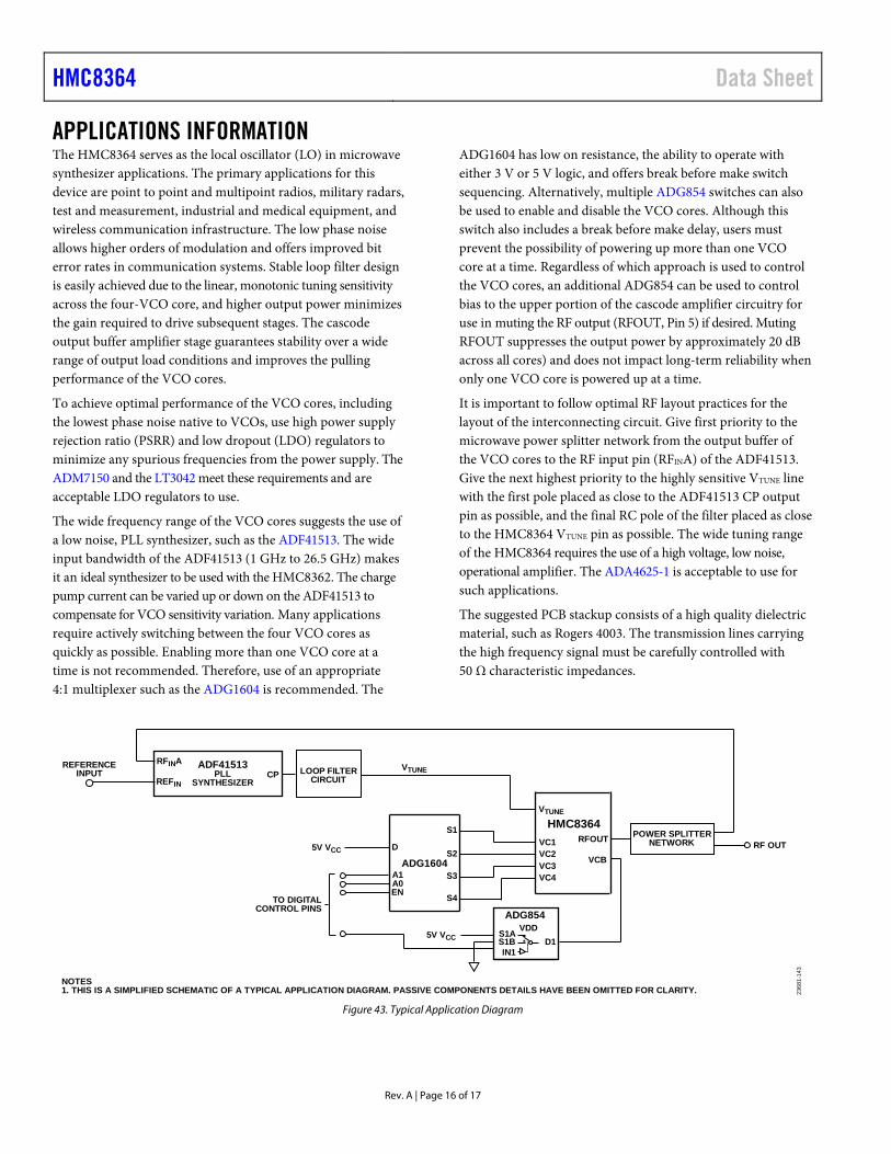
THEORY OF OPERATION The HMC8364 consists of four, fundamental VCOs with overlapping frequency ranges to ensure continuous frequency coverage from 18.10 GHz to 26.60 GHz over all conditions.
Using four oscillators instead of a single oscillator to span the frequency range reduces the percent bandwidth and tuning sensitivity of each oscillator, improving phase noise performance. Tuning sensitivity flatness across the frequency range is also improved and simplifies the loop filter design in synthesizer applications. The tuning sensitivity is similar across the four VCO cores, which means that the loop bandwidth and phase margin of the loop filter vary less overall vs. a single oscillator solution.
The four oscillators share a common tuning port, which means that even though the active devices in unused VCO cores are not biased, the resonant tanks of all four VCO cores are in
parallel and tuned simultaneously. A single buffer amplifier is also shared by all four VCOs.
The upper circuitry of the buffer amplifier is biased by VCB (Pin 8). The lower portion of the cascode buffer amplifier remains off and very little current flows until one of the VCO cores is enabled.
The lower circuitry of the amplifier is enabled when the RF signal of any one of the four VCOs arrives at its input. If VCB is biased and any VCO core is enabled, current flows through the buffer amplifier and the RF signal propagates to RFOUT (Pin 5).
The buffer amplifier is designed to support only one VCO at a time. Avoid enabling more than one oscillator at a time because multiple oscillators stress the buffer amplifier enough to reduce its long-term operating life.
HMC8364 Data Sheet
Rev. A | Page 16 of 17
APPLICATIONS INFORMATION The HMC8364 serves as the local oscillator (LO) in microwave synthesizer applications. The primary applications for this device are point to point and multipoint radios, military radars, test and measurement, industrial and medical equipment, and wireless communication infrastructure. The low phase noise allows higher orders of modulation and offers improved bit error rates in communication systems. Stable loop filter design is easily achieved due to the linear, monotonic tuning sensitivity across the four-VCO core, and higher output power minimizes the gain required to drive subsequent stages. The cascode output buffer amplifier stage guarantees stability over a wide range of output load conditions and improves the pulling performance of the VCO cores.
To achieve optimal performance of the VCO cores, including the lowest phase noise native to VCOs, use high power supply rejection ratio (PSRR) and low dropout (LDO) regulators to minimize any spurious frequencies from the power supply. The ADM7150 and the LT3042 meet these requirements and are acceptable LDO regulators to use.
The wide frequency range of the VCO cores suggests the use of a low noise, PLL synthesizer, such as the ADF41513. The wide input bandwidth of the ADF41513 (1 GHz to 26.5 GHz) makes it an ideal synthesizer to be used with the HMC8362. The charge pump current can be varied up or down on the ADF41513 to compensate for VCO sensitivity variation. Many applications require actively switching between the four VCO cores as quickly as possible. Enabling more than one VCO core at a time is not recommended. Therefore, use of an appropriate 4:1 multiplexer such as the ADG1604 is recommended. The
ADG1604 has low on resistance, the ability to operate with either 3 V or 5 V logic, and offers break before make switch sequencing. Alternatively, multiple ADG854 switches can also be used to enable and disable the VCO cores. Although this switch also includes a break before make delay, users must prevent the possibility of powering up more than one VCO core at a time. Regardless of which approach is used to control the VCO cores, an additional ADG854 can be used to control bias to the upper portion of the cascode amplifier circuitry for use in muting the RF output (RFOUT, Pin 5) if desired. Muting RFOUT suppresses the output power by approximately 20 dB across all cores) and does not impact long-term reliability when only one VCO core is powered up at a time.
It is important to follow optimal RF layout practices for the layout of the interconnecting circuit. Give first priority to the microwave power splitter network from the output buffer of the VCO cores to the RF input pin (RFINA) of the ADF41513. Give the next highest priority to the highly sensitive VTUNE line with the first pole placed as close to the ADF41513 CP output pin as possible, and the final RC pole of the filter placed as close to the HMC8364 VTUNE pin as possible. The wide tuning range of the HMC8364 requires the use of a high voltage, low noise, operational amplifier. The ADA4625-1 is acceptable to use for such applications.
The suggested PCB stackup consists of a high quality dielectric material, such as Rogers 4003. The transmission lines carrying the high frequency signal must be carefully controlled with 50 Ω characteristic impedances.
RFOUT
ENA0A1 S3
S4
S2
S1VC1
VTUNE
VC2VC3VC4
VCB
D1VDD
S1BIN1
S1A
RF OUT
VTUNE
HMC8364
ADG854
ADG1604
TO DIGITALCONTROL PINS
ADF41513PLL
SYNTHESIZERLOOP FILTER
CIRCUITREFERENCE
INPUT
5V VCC
5V VCC
D
REFIN
RFINACP
POWER SPLITTERNETWORK
NOTES1. THIS IS A SIMPLIFIED SCHEMATIC OF A TYPICAL APPLICATION DIAGRAM. PASSIVE COMPONENTS DETAILS HAVE BEEN OMITTED FOR CLARITY. 23
681-
143
Figure 43. Typical Application Diagram

Data Sheet HMC8364
Rev. A | Page 17 of 17
OUTLINE DIMENSIONS
08-2
2-20
18-A
0.50BSC
BOTTOM VIEWTOP VIEW
SIDE VIEW
EXPOSEDPAD
0.05 MAX0.02 NOM
0.20 REF
4.50 REF
COPLANARITY0.08
0.300.250.20
6.106.00 SQ5.90
0.900.850.80
0.20 MIN
4.754.70 SQ4.65
401
11 102021
3031
PKG
-004
893
FOR PROPER CONNECTION OFTHE EXPOSED PAD, REFER TOTHE PIN CONFIGURATION ANDFUNCTION DESCRIPTIONSSECTION OF THIS DATA SHEET.
SEATINGPLANE
PIN 1IN D ICATO R AR E A OP TIO N S(SEE DETAIL A)
DETAIL A(JEDEC 95)
*COMPLIANT TO JEDEC STANDARDS MO-220-VJJD-5WITH EXCEPTION TO LEAD LENGHT
PIN 1INDICATOR
AREA
*0.350.300.25
Figure 44. 40-Lead Lead Frame Chip Scale Package [LFCSP]
6 mm × 6 mm Body and 0.85 mm Package Height (HCP-40-1)
Dimensions shown in millimeters
ORDERING GUIDE
Model1 Temperature Range MSL Rating2 Package Description Package Option
Ordering Quantity
HMC8364LP6GE −40°C to +85°C MSL3 40-Lead Lead Frame Chip Scale Package [LFCSP] HCP-40-1 HMC8364LP6GETR −40°C to +85°C MSL3 40-Lead Lead Frame Chip Scale Package [LFCSP] HCP-40-1 500 EV1HMC8364LP6G Evaluation Board 1 Z = RoHS Compliant Part. 2 See the Absolute Maximum Ratings section.
©2020 Analog Devices, Inc. All rights reserved. Trademarks and registered trademarks are the property of their respective owners. D23681-9/20(A)


![Frequency [GHz]](https://static.fdocuments.us/doc/165x107/56815d71550346895dcb7a09/frequency-ghz-56bc57e7b9bfb.jpg)


![Multiband LTE-A/WWAN Antenna for a Tablet · MHz - 862 MHz, 2.3 GHz - 2.4 GHz, 3.4 GHz - 4.2 GHz, 4.4 GHz - 4.99 GHz [1]. LTE-A provides much high-er data rate for real-time voice](https://static.fdocuments.us/doc/165x107/5e8aca7c2ae37b1267657c33/multiband-lte-awwan-antenna-for-a-tablet-mhz-862-mhz-23-ghz-24-ghz-34.jpg)