12 SEU/SET Tolerant Phase-Locked Loops · 12.4.1 Ring VCO ... Older literature on fault-tolerant...
20
12 .1 Introduction .................................................................................................. 293 12.2 Voting Asynchronous Signals .......................................................................294 12.3 Stable PLLs that Minimize Phase-Induced Voting Error ............................ 296 12.4 SEU/SET Characteristics of PLL Building Blocks ...................................... 302 12 .4.1 Ring VCO .........................................................................................302 12.4.2 Frequency Divider ............................................................................ 303 12.4.3 Sigma-Delta Fractional-N Frequency Dividers ................................ 303 12.4.4 Phase-Frequency Detector ................................................................304 12 .4.5 Charge Pumps ...................................................................................305 12 .4.6 Loop Filter ........................................................................................306 12.5 Applying Redundancy to PLLs .................................................................... 307 12.5.1 Output-Only Voting Method ............................................................ 308 12.5.2 The VCO Voting Method .................................................................309 12 .6 Conclusions ...................................................................................................311 References .............................................................................................................. 311 12 SEU/SET Tolerant Phase-Locked Loops Robert L. Shuler, Jr. contents 12.1 IntroductIon The phase-locked loop (PLL) is an old and widely used circuit for frequency and phase demodulation, carrier and clock recovery, and frequency synthesis [1]. Its implementations range from discrete components to fully integrated circuits and even to firmware or software. Often the PLL is a highly critical component of a system, as for example when it is used to derive the on-chip clock, but as of this writing no definitive single-event upset (SET)/single-event transient (SET) tolerant PLL circuit has been described. This chapter hopes to rectify that situation, at least in regard to PLLs that are used to generate clocks. Older literature on fault-tolerant PLLs deals with detection of a hard failure, which is recovered by replacement, repair, or manual restart of discrete component systems [2,3]. Several patents exist along these lines (6349391, 6272647, and 7089442). A newer approach is to harden the parts of a PLL system, to one degree or another, such as by using a voltage-based charge pump [4,5] or a triple modular redundant (TMR) Au: “voted” seems out voted voltage-controlled oscillator (VCO) [6]. A more comprehensive approach is to of place here. harden b triplication and voting TMR all the digital pieces (primarily the divider Y P g( ) g P^ (P Y ) 293 K11326_C012.indd 293 1/29/10 3:38:57 PM https://ntrs.nasa.gov/search.jsp?R=20100017265 2018-07-16T18:24:22+00:00Z
Transcript of 12 SEU/SET Tolerant Phase-Locked Loops · 12.4.1 Ring VCO ... Older literature on fault-tolerant...

12 .1 Introduction .................................................................................................. 29312.2 Voting Asynchronous Signals .......................................................................29412.3 Stable PLLs that Minimize Phase-Induced Voting Error ............................ 29612.4 SEU/SET Characteristics of PLL Building Blocks ...................................... 302
12 .4.1 Ring VCO .........................................................................................30212.4.2 Frequency Divider ............................................................................ 30312.4.3 Sigma-Delta Fractional-N Frequency Dividers ................................ 30312.4.4 Phase-Frequency Detector ................................................................30412 .4.5 Charge Pumps ...................................................................................30512 .4.6 Loop Filter ........................................................................................306
12.5 Applying Redundancy to PLLs .................................................................... 30712.5.1 Output-Only Voting Method ............................................................ 30812.5.2 The VCO Voting Method .................................................................309
12 .6 Conclusions ...................................................................................................311References .............................................................................................................. 311
12 SEU/SET TolerantPhase-Locked Loops
Robert L. Shuler, Jr.
contents
12.1 IntroductIon
The phase-locked loop (PLL) is an old and widely used circuit for frequency andphase demodulation, carrier and clock recovery, and frequency synthesis [1]. Itsimplementations range from discrete components to fully integrated circuits andeven to firmware or software. Often the PLL is a highly critical component of asystem, as for example when it is used to derive the on-chip clock, but as of thiswriting no definitive single-event upset (SET)/single-event transient (SET) tolerantPLL circuit has been described. This chapter hopes to rectify that situation, at leastin regard to PLLs that are used to generate clocks.
Older literature on fault-tolerant PLLs deals with detection of a hard failure, whichis recovered by replacement, repair, or manual restart of discrete component systems[2,3]. Several patents exist along these lines (6349391, 6272647, and 7089442). Anewer approach is to harden the parts of a PLL system, to one degree or another, suchas by using a voltage-based charge pump [4,5] or a triple modular redundant (TMR)
Au: “voted” seems out voted voltage-controlled oscillator (VCO) [6]. A more comprehensive approach is toof place here.
harden b triplication and voting TMR all the digital pieces (primarily the dividerY P g( ) g P^ (P Y )
293
K11326_C012.indd 293 1/29/10 3:38:57 PM
https://ntrs.nasa.gov/search.jsp?R=20100017265 2018-07-16T18:24:22+00:00Z

Radiation Effects in Semiconductors294
of a frequency synthesis PLL [7], but this still leaves room for errors in the VCO andthe loop filter.
Instead of hardening or voting pieces of a system, such as a frequency synthesissystem (i.e., clock multiplier), we will show how the entire system can be voted.There are two main ways of doing this, each with advantages and drawbacks. Wewill show how each has advantages in certain areas, depending on the lock acquisi-tion and tracking characteristics of the PLL. Because of this dependency on PLLcharacteristics, we will briefly revisit the theory of PLLs. But first we will describethe characteristics of voters and their correct application, as some literature does notfollow the voting procedure that guarantees elimination of errors. Additionally, wewill find that voting clocks is a bit trickier than voting data where an infallible clockis assumed. It is our job here to produce (or recover) that assumed infallible clock!
12.2 VotIng Asynchronous sIgnAls
When voting synchronous signals, data are latched according to a clock edge andcan be unambiguously voted either before or after the clock edge. There are twocommon ways of doing this, according to what is to be protected. Figure 12.1 showsthe two methods.
On the left we have a triplicated functional unit (usually memory, but could beanything). A single voter removes errors introduced within any one of the units butdoes not protect against errors in the voter itself or in anything prior to the triplicatedunits. On the right everything is triplicated, including the voters, so all errors areremoved. As long as two of the three strings have a correct result, processing willcontinue correctly.
When voting asynchronous signals, those such as clocks that are not synchro-nized by some other signal, it is possible to have two correct signals and still getan incorrect result. Suppose, for example, that “correct” means a signal of a givenfrequency, such as the output of a clock multiplier. In Figure 12.2, signals X and Yare correct, and signal Z is in error. But because X and Y are not perfectly in phase,Z is able to influence the vote this way and that, producing anomalous results for thevoting result (maj – top signal), which is of incorrect frequency and has some transi-tions that are much too fast. These extra transitions will violate timing constraintsand produce unpredictable errors if they occur on a clock signal.
FIgure 12.1 Single versus triple voters.
K11326_C012.indd 294 ^ 1/29/10 3:38:58 PM

v(maj)
v(z)
v(y)
v(x)
SEU/SET Tolerant Phase-Locked Loops 295
0 5 10 15 20
Time (ns)
FIgure 12.2 Phase-induced voting error.
While this example has been exaggerated for illustration, such an error can occureven for a small phase difference between the two correct signals. To guarantee thatextra-transition errors (phase-induced voting error) will not occur, the phase dif-ference between the two correct signals has to be smaller than the minimum pulsewidth to which the voters will respond!
The voting guidelines we have so far may be summarized as (1) use a triple voterconfiguration to protect against errors even in the voters, and (2) design your PLL sothat redundant units will operate closely enough in phase that phase-induced votingerrors will be avoided, as for example during the period when one unit is recoveringfrom an SEU/SET and running temporarily at a different frequency or with glitchesin its output. One more guideline is needed. What do you do if ultimately you wish toget one reliable output, such as one system master clock? In this case you must eventu-ally rely on a single voter (though you can still use triple voters internal to your PLLsystem). The only type of voter that does not have a single SEU/SET susceptible pointof failure is a heavily overdriven force voter, or conflict voter, that uses many gates todrive a single node. These gates should be spread out so that one single event will notstrike several of them, and they should be driven from independent sources, such as atriple of prevoters. A rather elaborate example I have used is shown in Figure 12.3.
FIgure 12.3 Force voter for consolidating triple to single string.
K11326_C012.indd 295 ^ 1/29/10 3:39:00 PM

Radiation Effects in Semiconductors296
QBHigh 2-Input Transition Nand Gate
Symbol (A designates input to central pair)
A AQBlow 0
B ^ ^
FIgure 12.4 Transition nAnd gate.
The special symbol in Figure 12.3 is not a NAND gate. It is a transition nAndgate (TAG) [8,9], also sometimes called a guard gate [10,11], broadly useful inradiation-hardening-by-design (RHBD) technology. The circuit for it is shown inFigure 12.4.
12.3 stAble Plls thAt MInIMIzePhAse-Induced VotIng error
A PLL is a feedback circuit that measures the phase of a signal compared with somereference and attempts to correct the phase of a local oscillator to match the reference.The local oscillator is frequently a VCO but may also be a numerically controlledoscillator, and in signal processing applications the whole PLL may be implementedmathematically in firmware rather than using actual components. But when a PLLmust operate very fast and produce the clock on which digital logic depends, there isno alternative but to implement it directly in hardware.
An analysis of charge-pump PLLs by Gardner [14] points out several stability Au: Refs 12 and 13need to be cited before
issues. First, the continuous-time approximation used for the analysis is not valid ref 14. Please revise.
if the PLL loop bandwidth is high, and this introduces stability problems. Forthe fastest recovery from SEU/SET tolerance we will want the highest bandwidthpractical. For clock generator PLL applications, it turns out it is very practicalto increase loop bandwidth. For frequency synthesizer PLL applications, used togenerate channel frequencies for communications systems, higher loop bandwidth
K11326_C012.indd 296 ^ 1/29/10 3:39:01 PM

LL loopormal
SEU/SET Tolerant Phase-Locked Loops 297
P1
Frequency (Hz)
FIgure 12.5 PLL versus normal feedback loop bode plot.
is not so practical. We will examine redundant PLL architectures appropriate toboth situations.
Second, frequency synthesis PLLs need to have second- or third- or higher-orderloop filters to reduce ripple on the VCO control voltage, Vctl, caused by charge-pumpoperation and by the workings of fractional-N and sigma-delta frequency divid-ers and associated compensation systems. Whereas second-order analog PLLs areunconditionally stable, a second-order charge-pump-based PLL is a sampled datasystem and is unstable with high loop gain. The characteristics of VCOs currentlypreferred for high speed PLLs, which will be described in the next section, virtuallyguarantee excessively high gain unless the designer takes careful steps to ensureotherwise. With a third-order loop the situation is even worse. We will consider themost effective ways to manage loop gain.
Because of the additional pressure toward instability due to the requirements ofan SEU/SET tolerant PLL, we will briefly review PLL stability and introduce non-linear circuit considerations.
For any feedback loop to be stable and not oscillate, the feedback must be negativeat all frequencies for which the feedback loop gain is equal to or greater than unity.PLLs are rarely completely stable. Their residual instability, the reasons for whichwe will explore herein, shows up as continual oscillation in frequency, or phase, ofthe local oscillator. This residual instability is a source of excess phase jitter and canimpair the ability to synchronize redundant PLLs in a fault tolerant circuit, and thedesign techniques often used to combat it (lower bandwidth loop filters) can slow andinterfere with recovery from an SET or SEU.
Stability of a feedback circuit is often understood by means of a Bode plot, suchas in Figure 12.5. Loop gain is asymptotically plotted as a function of frequency.
60
40
20
v 0a
–20w0a –40
–60
–80
–100
K11326_C012.indd 297 ^ 1/29/10 3:39:02 PM

298
Radiation Effects in Semiconductors
Master (clock in)
FIgure 12.6 PLL block diagram with divider for frequency synthesis.
In the case of the PLL, this is the frequency with which the loop control voltagevaries, not the frequency of oscillation of the VCO. The two are related of courseby the transfer function of the VCO, which in the circuits we will be using is highlynonlinear.
First consider a normal operational amp (op amp) feedback loop, with loop gainrepresented by the dashed line. It is shown with two example poles in the loopresponse, N1 and N2. A 90 degree phase shift is associated with each pole. As longas no more than one pole is above the unity gain line, the circuit should be stable. Ifnot naturally the case, this is often arranged by use of a Miller effect equalizationcapacitor to move one pole lower in frequency than any others.
A PLL, on the other hand, does not control the same thing it measures. It mea-sures phase, but through the VCO it controls frequency. Phase is the integral of fre-quency. Therefore, every PLL has an unavoidable pole at zero frequency. You cannotmove any other pole below it! This is illustrated by the dotted line, with poles P1(infinitely off to the left on this logarithmic frequency scale plot) and P2. We haveoptimistically shown P2 below unity gain, but that is often difficult to arrange.
Unfortunately, determining gain for a highly nonlinear circuit is problematic. Thebest way is usually to run a transient simulation in Spice to see if the loop is stable.The point of this discussion is that one must be careful in designing the loop filterin a PLL. Below is a high-level block diagram level view of a PLL clock multiplier,in Figure 12.6.
Phase or phase-frequency detectors usually output a series of pulses, not a nicelybehaved analog signal, so the loop filter must be introduced to smooth this signal.Otherwise, the VCO would vary between some very high and very low frequency,and its output would be unusable. The loop filter determines the bandwidth of thePLL [1]. Here we get conflicting requirements. For recovery from SETs and SEUs,the loop filter should have a high bandwidth so that the PLL performs like a trackingPLL and rapidly resynchronizes after an upset. But in clock or synthesis applica-tions, a narrow frequency range is desired, meaning a low filter bandwidth. This is sothat the VCO deviation over the counter cycle of the frequency divider will be small.In a fractional-N or sigma-delta PLL, the VCO deviation over several counter cyclesmust be small. A low filter bandwidth slows acquisition, either initially or after anupset. Additionally, the loop filter forms a second pole in the loop gain, and a lowbandwidth loop filter moves that pole to the left on a Bode plot, toward a position ofhigher gain on the PLL’s unavoidable pole-at-zero loop response characteristic.
Sometimes PLLs are designed with a tight (low bandwidth) loop for normal oper-ation, and a separate means for initial “acquisition” of the target signal (the master
K11326_C012.indd 298 ^ 1/29/10 3:39:03 PM

1.11.00.90.80.70.60.5
c 0.40.30.20.10.0
–0.1
v(05)
v(Vctl)
SEU/SET Tolerant Phase-Locked Loops 299
clock, in the case of Figure 12.6). We do not recommend this for SEU/SET tolerantPLLs, because an SET or SEU can cause an unplanned reacquisition at any time.Having a separate means for acquisition might be possible but is difficult to verifyfor every case.
The requirement for unplanned reacquisition at any time implies that we shoulduse a phase-frequency detector (PFD), not a pure phase detector (e.g., XOR gate,traditional frequency multiplier). Phase-only detectors often are tricky to designfor initial or reacquisition, especially when using tight loop filters. The reason isthat without intrinsic frequency information, the phase-only detector can slip phaserepeatedly, and a tight loop filter will average the varying output of the phase-onlydetector and produce false lock. The tighter the loop filter, the closer the false lockfrequency can be to the desired frequency. It does not have to be at a harmonic of thedesired frequency.
A frequency synthesis or clock generator PLL can easily find itself operatingin the unstable region. The tight loop filter needed to control the frequency of thesynthesized signal, coupled with the inherently high gain of some high-speed VCOs(which we will describe in the next section), places their loop filter pole above unitygain. If the instability is small, they work anyway. A PFD is not a pure phase detec-tor, so to some extent the unfortunate pole-at-zero is eliminated, but not completely.But over the region where the PFD functions as a phase detector, basically when thePLL is “locked” and tracking its input, the PLL control loop oscillates, producingunwanted phase jitter. If this source of jitter can be reduced below the cycle drivenjitter (from alternating pulses out of the charge pump), it is no longer a concern. Butchanging the loop parameters to make a PLL more SEU/SET tolerant can increaseinstability. Figure 12.7 shows a plot of this instability in an original case and withsome modifications that a designer might use to minimize the jitter.
A quick way to understand what is going on in a PLL is to examine the loopcontrol voltage (Vctl in Figure 12.6), that is, the input to the VCO. In Figure 12.7 thisis the dark wavy line. Ideally the line would be flat, indicating no variation in the
Original Loop Filter 25x Lower Loop Filter Lower Gain via Higher Vctl
0.5 0.6 0.7
5 6 7 1.0 ??
Time (us)
FIgure 12.7 PLL instability management, comparing approaches.
K11326_C012.indd 299 ^ 1/29/10 3:39:04 PM

Radiation Effects in Semiconductors300
(oscillator feedback)
FIgure 12.8 Current-starved inverter loop VCO.
frequency the VCO is requested to produce. A common type of VCO used in high-speed complementary metal-oxide semiconductor (CMOS) PLLs is the current-starved inverter loop, such as shown in Figure 12.8.
The transfer characteristic of this type of VCO is such that when Vctl is near thethreshold voltage, a very wide variation in frequency occurs for tiny changes in Vctl.
In other words, the voltage-to-frequency gain (often denoted Kvco) is very high nearVthreshold . A small Kvco is beneficial in achieving low phase noise [15].
Kvco is not only high near Vthreshold; it is rapidly varying (i.e., highly nonlinear),which in itself can cause stability problems [14]. The plots of Figures 12.7a, 12.7b,and 12.7c were obtained using the schematic of a well-designed PLL, but operatingit at a lower than designed master input clock frequency so that Vctl would be too lowand the loop gain very high. The result is Figure 12.7a in which a steady oscillationin Vctl produces a frequency instability that is unacceptable.
An alternative to the current-starved inverter VCO is a tank circuit. These typicallyhave smaller Kvco but also more narrow tuning ranges. And the necessity of having aninductor makes them less desirable for fully integrated or redundant applications.
Figure 12.7b shows what happens if one uses the instinctive solution feedbackcircuit designers would apply, that is, to “compensate” or dramatically lower the polethat the designer can control, the loop filter cutoff frequency. This is lowered by afactor of 25 in the middle figure. It appears to help slightly, perhaps by a factor oftwo, but the acquisition and tracking characteristics are dramatically reduced, in factby a factor of 25! So while this sort of works, it might conflict with SEU/SET recov-ery performance requirements. Why doesn’t this technique work better? It is becausethe PFD is highly nonlinear. A large frequency deviation can have approximately the
K11326_C012.indd 300 ^ 1/29/10 3:39:05 PM
SEU/SET Tolerant Phase-Locked Loops 301
same PFD output as a modest deviation. This makes the loop less sensitive than itshould be to changes in the loop bandwidth.
Figure 12.7b shows what happens if instead of tampering with the loop filter, welower the VCO gain. Since the gain, if we are using a current-starved inverter VCO,is determined by the bias of Vctl, we must figure how to raise Vctl. This can be done bymaking the VCO slower, so a higher Vctl is needed to operate at the desired frequency.To achieve this, 2.5 pF of capacitance was added to nodes O2 and O3. Modifying atleast two nodes, and an even number of them, assures a symmetric waveform withinthe VCO, and that one node is not operated far beyond its cutoff frequency. Onecould modify all nodes if one wished. Adding stages to the VCO is not a particularlyeffective alternative for raising Vctl, because very many stages are required. Makingthe circuit larger also would increase its SEU/SET error cross section.
Adding capacitance raised Vctl from around 0.46 V to 0.8 V, and the output fre-quency stability was vastly improved. This was accomplished without significantdegradation of the acquisition and tracking characteristics of the PLL! It might seemto an experienced feedback loop designer that changing the loop filter or loop gainto have a given stability effect should be more equivalent. But due to the nonlinearnature of the PFD, changes to the VCO predominantly affect stability, not acquisi-tion. When there is a frequency mismatch between the VCO and the reference input,the PFD outputs either low or high, with no indication of how low or how high. So,excess gain in the VCO increases the frequency error without increasing the track-ing “force.”
Figure 12.7d shows a charge-pump PLL in acquisition mode. Notice that Vctl
jogs around in an irregular way, due to the nonlinear interactions among theVCO, PFD, and loop filter. It may take a long time for this to stabilize. Duringacquisition, a frequency deviation is produced by the PLL to bring phase into amatching condition. At match, the PFD produces no output. The phase momen-tarily matches. But the frequency deviation persists until enough phase erroraccumulates to drive the loop back the other way. For stability, one must guar-antee this process eventually damps out, which may require a very slow (lowbandwidth) loop, not what we’d like for fast SEU/SET recovery. There are fourparameters by which such a “slow” PLL might be judged: acquisition time, jitter,spectral purity, and phase error (with regard to the input reference). In the slowdesign, both acquisition time and phase error are traded for jitter and spectralpurity. A small and varying phase error would be of no consequence in clockgenerator applications of a PLL. But in a redundant voted PLL, if the three com-ponent PLLs have independent phase errors, then phase-induced voting errorcan result.
Figure 12.7e shows a PLL in which the PFD is modified to always produce anoutput. This is done by presuming that if the phase is not ahead, it is behind, so thePFD is always outputting a signal, or “always on.” Such an architecture reintroducesthe drawbacks of older more linear PLLs (the phase error bias), but notice that italso has a more linear behavior without the chaotic jogs of the classic three-statePFD. It is also free of dead-zone nonlinearity near-zero phase error and is easier toanalyze. Figure 12.7f combines VCO gain reduction with the always-on PFD to pro-duce a very well-behaved loop. A clever designer could match the Vctl of the desired
K11326_C012.indd 301 ^ 1/29/10 3:39:05 PM
Radiation Effects in Semiconductors302
operating frequency of the VCO to the 50% duty cycle of the always-on PFD to cre-ate a PLL that would have no static phase error, low jitter, and also quick recoveryfrom SEU/SET.
The faster a PLL acquires, the faster it will recover from an SEU/SET. Recoverytime is important in a voting arrangement, because while one module is recovering, asecond SEU/SET will cause an output error. Tight phase tracking is important to pre-vent phase-induced voting error. The key to making a good redundant fault-tolerantPLL is to start with a fast acquisition, low phase error, and single-string PLL design.
12.4 seu/set chArActerIstIcs oF Pll buIldIn g blocks
Figure 12.6 shows five building blocks in a basic PLL for frequency synthesis. Wedescribe the ring VCO in connection with Figure 12.8. The other four blocks can inprinciple be anything the designer chooses, but we discuss a representative designof each block here for purposes of understanding how their SEU/SET characteristicsmight affect our overall design.
12.4.1 Ring VCO
The SEU/SET characteristic of the Ring VCO is straightforward and somewhatunfortunate. It comes to an erroneous phase, from which it does not return on itsown. Each stage of the VCO has four transistors, about as many as a typical digitallogic gate. There are usually at least 5 stages, and sometimes 10 or more, so the crosssection of the VCO rivals that of any other part of the PLL, such as the frequencydivider. To make matters worse, the VCO is operated in current starved mode, whichmeans that less current is available for charge clearing after an ion strike than wouldbe the case in a high drive digital circuit.
Furthermore, an SET in any part of the VCO causes a phase displacement,whereas in a digital circuit only half the circuit is susceptible most of the time. Thisat least doubles the error cross section of the VCO. There are three effects in play. Ina digital circuit with multiple input gates, the state of the logic ignores many of theinputs. For example, a NAND gate with one input low effectively ignores the secondinput and any error on the second input. The VCO stages do have multiple inputs (thesignal and the control voltage), but neither of them is ever ignored.
Second, digital logic transistors that are in the ON or conducting state do notexperience a state change when an ion strikes, because ion strikes only increase con-duction and do not decrease it. If the excess charge is cleared by the time the statechanges, no effect is noticed. Timing of the digital logic is important only insofaras it meets minimum timing requirements. However in the VCO timing of the delaythrough each stage is always critical. Even a slight change in timing due to extra timerequired to clear charge from an ion strike will result in clock jitter and possible tim-ing violations in the target circuit served by the clock.
Third, digital logic is sampled by the clock, and errors are counted only if theypersist through a clock edge. But the clock, and thus the VCO, is not sampled byanything, and errors occurring at any time may result in system errors.
K11326_C012.indd 302 ^ 1/29/10 3:39:05 PM

SEU/SET Tolerant Phase-Locked Loops 303
The first goal of an SEU/SET tolerant design is to quickly return the VCO to acorrect state. This should be done regardless of the method of eliminating errors. If,for example, one of three VCOs lingers in an incorrect state, the chances it will causephase-induced voting error increase. If it lingers long enough, there may even be asecond SEU/SET in another part of the circuit, causing an error.
There are several ways of quickly returning a VCO to a correct state, and in latersections we will explore two of them in detail. One method is to use PLL parametersthat produce fast acquisition and tracking. Presumably this will also result in fastcorrection. Fast correction will not prevent an error on the output and so must beused in combination with some other scheme for eliminating errors. But it will pre-vent the VCO from lingering in an incorrect state and thus minimize the probabilityof phase-induced voting error, or accumulation of a second error. The problem withfast acquisition and tracking is that, as described already, it is often at odds withfrequency and phase stability, or tightness of tracking.
Another method of quickly returning a VCO to a correct state is to have threeVCOs and vote them [12]. This works so quickly that it also eliminates errors.However, it eliminates only errors from the output of the VCO, if taken from thevoter output, not from other parts of the PLL. Still another method is to vote only theoutput of the entire PLL (with two other identical PLLs) and to allow the feedbackloop to resynchronize any PLL that experiences an SEU/SET induced error. We willexplore both of these in a subsequent section.
12.4.2 FRequenCy DiViDeR
The frequency divider, needed when the PLL is to provide frequency synthesis, is adigital state machine, and an SEU putting it in a different state is probably the mostdisruptive of any SEU/SET effect in a PLL. It is possible of course to vote every bitin the state machine [7]. Or one can allow the feedback loop of the PLL to eventuallyresynchronize the divider by reacquiring lock on the master clock input. In eithercase, a divider that minimizes SEU susceptibility is a good idea, such as a fullysynchronous design.
It is very important to note that if the frequency divider is protected by voting,this cannot be done using the same components that otherwise participate in someother PLL voting scheme. For example, if three complete PLLs are voted, differ-ences in the frequency dividers are essential to allow a failed PLL to resynchronizeitself with the others.
12.4.3 S igma-Delta FRaCtiOnal-n FRequenCy DiViDeRS
Sigma-delta or fractional-N frequency dividers use a dithering scheme to divide theVCO frequency by a sequence of integers that averages to a noninteger value. Thiscreates two problems for the designer of a fault tolerant PLL. First, there is a lotmore logic in the frequency divider, which must be protected from SEU/SET. This isinconvenient but not conceptually difficult. If voting is used, care must be taken thatno internal state is left unprotected and allows an error to persist.
K11326_C012.indd 303 ^ 1/29/10 3:39:06 PM

Radiation Effects in Semiconductors304
Second, either the variability of the output of the dithered frequency divider mustbe averaged over a longer period, implying a lower bandwidth loop filter and leadingto problems we have already discussed, or compensation circuitry must be used totune out the expected variations. Compensation circuitry can be analog in nature,getting involved with the charge pump, and can be both more susceptible to SET andmore difficult to protect. A strategy of protecting an entire PLL is advantageous forsuch a situation. In the case where this circuit is protected by voting, care must betaken to vote every internal state variable so that there are no persistent errors.
12.4.4 PhaSe-FRequenCy DeteCtOR
There are many types of phase detectors and phase-frequency detectors [1,13]. Forclock recovery PLLs, which examine data transitions and synthesize the impliedclock, a PFD that tolerates missing transitions is required. For frequency synthesis,we are already in the position that the PLL is generating many more transitions thanare in the master clock and, so for synthesis, PFDs are desired that use every clockedge, both leading and trailing, and produce immediate correction signals if the edgeis leading or lagging. In the interest of setting a manageable scope for the currentdiscussion, we limit ourselves to the second type. These are usually three-state orhigher-logic circuits. While better acquisition performance can be obtained withcomplex higher-state PFDs, the additional states also increase SEU susceptibility andincrease the difficulty of resynchronization. An ordinary three-state PFD as shownin Figure 12.9 always resets itself when a clock edge has occurred on both inputs.
For most radiation-tolerant applications, we would use fully synchronous flip-flops. However, this PFD circuit works only with an asynchronous reset. The circuitof Figure 12.9 updates on leading edges of master and slave signals. One sourceof phase jitter in a frequency synthesizer is the PFD update cycle, because Vctl willtypically vary from some minimum to maximum value between PFD updates. Theupdate cycle can be cut in half, reducing phase jitter, by using two PFD circuits andnegating the inputs to the second one so that it updates on trailing (falling) edges.
D Q 1 111, Fast
Slave I QB
(from frequency divider)resetb
^- Clb
D Q SlowDFFC
Master QB
FIgure 12.9 Single-edge three-state PFD.
K11326_C012.indd 304 ^ 1/29/10 3:39:07 PM

SEU/SET Tolerant Phase-Locked Loops 305
As soon as both flip-flops have triggered (i.e., an edge is detected on both inputsignals) the flip-flops are reset, clearing any SEU condition.
12.4.5 ChaRge PumPS
There is a bit of an overlap when both the signals “fast” and “slow” are high,because of the time it takes the reset to operate. In a high-speed PLL this can be asignificant error factor. If perfect charge pumps are used, in theory the “fast” and“slow” signals each result in a fixed current pulse into the loop filter and cancelout. But current-oriented charge pumps are relatively more susceptible to SEU/SETthan a voltage-oriented charge pump (voltage with a high impedance switch) [4].The larger number of transistors in a near-ideal current pump, and their lower drivestrengths, increase both the exposure to SETs and the time required for recoveryfrom SETs.
In the case of the voltage-oriented charge pump, the overlapping “fast” and “slow”signals do not exactly cancel, and phase error is produced. This can be eliminated byusing pulse trimmers to reduce the length of these two signals by exactly the amountof the reset delay. Figure 12.10 shows a trimmer circuit that uses the same flip-flopreset to time the amount of trimming. Figure 12.11 shows the complete dual-edgePFD with trimmers and voltage-oriented charge pumps (switches are minimum-sizepass gates).
A good bit of the literature on precision PLL design, such as frequency synthe-sizers for communication circuits, depends on a sophisticated current-based chargepump with precisely matched currents. There are a couple of approaches for dealingwith this situation. One is to simply use the strategy of protecting the entire PLL,as we have been advocating, rather than its parts. SET recovery time will not befast, but there will be errors only if a second SET occurs before the recovery fromthe first is complete. While this would be disastrous in a clock circuit, it is probablyacceptable in a communication circuit where the communication protocol providesother means of handling errors. In other words, SEU/SET performance of frequencysynthesizers is less critical than for clock generator circuits.
FIgure 12.10 Reset pulse trimming circuit.
K11326_C012.indd 305 ^ 1/29/10 3:39:08 PM

(frc
Radiation Effects in Semiconductors306
FIgure 12.11 Dual-edge PFD with voltage-based charge pump.
A second strategy is to address issues with the voltage-based charge pump.Unbalanced charge injection can be addressed by Vctl tuning as already described,although this might be hard to make process-independent. Power supply noise isalso a commonly voiced concern for voltage-based charge pumps (though also forcurrent-based pumps). Lee and Wang [16] have shown significant benefits from usingseparate regulators for the VCO and the charge pump.
12.4.6 lOOP FilteR
The last block of the PLL is the loop filter. As emphasized, the ideal loop filter wouldnot be anything more than a single-pole RC filter. Second- and third-order loop fil-ters will lead to longer acquisition time and also longer recovery times from SET/SET errors. With the description in Section 12.3 of how PLLs can be stabilized, onemay be able to solve phase jitter problems by modifying the VCO gain. If necessary,the always-on PFD technique could be used. However, as with the charge pump, alarge amount of technical literature would have to be disregarded to follow our mostaggressive recommendation. We caution only that, when using a higher-order filter,make sure to examine the SET recovery time. If an SET disturbance causes millisec-onds of thrashing around, consider reducing the VCO gain.
Another consideration is simulation time. If you are designing a nonredundantPLL, it is sufficient to get one correct simulation for each frequency of operation, and
K11326_C012.indd 306 ^ 1/29/10 3:39:09 PM

SEU/SET Tolerant Phase-Locked Loops 307
I PFD_CP
(from chargeW = 3'1L = 100'1L = 100'1W = 3'1
(to VCO)
Vctl
5pF
Cap only
r,
FIgure 12.12 Loop filter.
you are done. But when designing a fault-tolerant PLL, it is necessary to considerthe response to a variety of faults, increasing the number of simulations. In eachsimulation, one must wait for acquisition, inject a fault, and wait for it to settle, soeach simulation is longer. It is tempting to incompletely verify the design in such asituation. The techniques we have outlined to reduce acquisition time will greatlyspeed up verification by allowing shorter simulations.
Ideally the RC loop filter would be just resistors and capacitors. In practice, in aCMOS circuit you can obtain an approximate RC filter by using resistor-connectedfield-effect transistors (FETs) for the resistor and the gates of FETs for the capacitor.This has the advantage of being process-independent and relatively scalable, pos-sibly requiring no change when moving to new processes.
Figure 12.12 shows such a loop filter. It is important to use a symmetric pair ofresistor connected FETs connected in opposite directions to avoid a nonlinear pref-erence for charging the filter in one direction or another. This circuit uses a width/
Au:Long form of length (W/L) of 3/100, giving quite a high impedance. Because of threshold voltages,W LOW
the circuit will not quite charge to either supply rail. For the capacitor, enough FETswith large area gates are connected in parallel to make whatever value is needed.
It would seem that an SET in the loop filter might be significant, but in practice itmight be of less consequence. If there is a lot of charge stored on the capacitor com-pared with the charge generated by an ion strike, an SET has less effect. Any effectit does have will be eliminated by the redundant voting techniques that will be usedto protect other parts of the circuit.
12.5 APPlyIng redundAncy to Plls
It is possible to improve or vote or otherwise mitigate SEU/SET for the individ-ual components of PLLs. This usually leaves some component, such as the loop
K11326_C012.indd 307 ^ 1/29/10 3:39:10 PM
Radiation Effects in Semiconductors308
VOx vote
VOy vote
VOzvote
In OutRing VCO
Control
In OutRing VCO
Control
In OutRing VCO
Control
FJ Phase Loop
Det. Filter
Phase LoopDet. Filter
Phase LoopDet. Filter
Master(clock in)
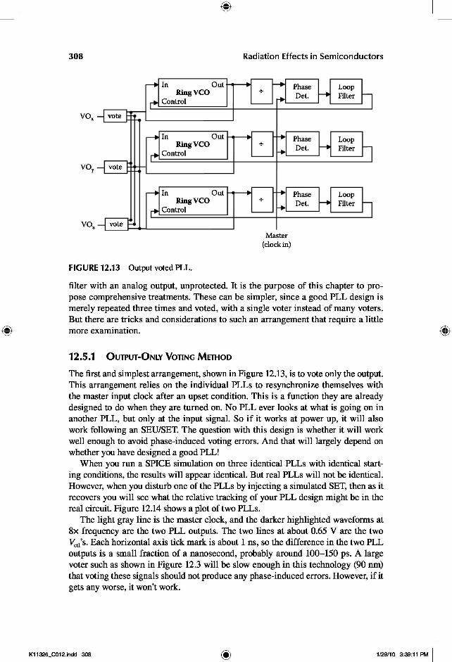
FIgure 12.13 Output voted PLL.
filter with an analog output, unprotected. It is the purpose of this chapter to pro-pose comprehensive treatments. These can be simpler, since a good PLL design ismerely repeated three times and voted, with a single voter instead of many voters.But there are tricks and considerations to such an arrangement that require a littlemore examination.
12.5.1 OutPut-Only VOting methOD
The first and simplest arrangement, shown in Figure 12.13, is to vote only the output.This arrangement relies on the individual PLLs to resynchronize themselves withthe master input clock after an upset condition. This is a function they are alreadydesigned to do when they are turned on. No PLL ever looks at what is going on inanother PLL, but only at the input signal. So if it works at power up, it will alsowork following an SEU/SET. The question with this design is whether it will workwell enough to avoid phase-induced voting errors. And that will largely depend onwhether you have designed a good PLL!
When you run a SPICE simulation on three identical PLLs with identical start-ing conditions, the results will appear identical. But real PLLs will not be identical.However, when you disturb one of the PLLs by injecting a simulated SET, then as itrecovers you will see what the relative tracking of your PLL design might be in thereal circuit. Figure 12.14 shows a plot of two PLLs.
The light gray line is the master clock, and the darker highlighted waveforms at8× frequency are the two PLL outputs. The two lines at about 0.65 V are the twoVctl ’s. Each horizontal axis tick mark is about 1 ns, so the difference in the two PLLoutputs is a small fraction of a nanosecond, probably around 100–150 ps. A largevoter such as shown in Figure 12.3 will be slow enough in this technology (90 nm)that voting these signals should not produce any phase-induced errors. However, if itgets any worse, it won’t work.
K11326_C012.indd 308 1/29/10 3:39:11 PM

1.11.00.90.80.70.60.50.40.30.20.10.0
–0.10.705 0.710 0.715 0.720
SEU/SET Tolerant Phase-Locked Loops 309
VCO Simulation
Time (us)
FIgure 12.14 Comparing outputs of identical PLLs after disturbance.
The thing that might make it get worse is trying to fix a stability problem by dra-matically lowering the loop filter bandwidth. This makes the control loop very slow,and it could be a long time, if ever, before the outputs line up again. Whether youfix stability problems by lowering the VCO gain or with the loop filter, you shouldcarefully check the worst-case disturbances to make sure your PLL outputs will lineup again. You can also check for the effect of process variation by changing the W/Lof a bias transistor in one of the ring VCOs by an amount of half a lambda, or halfthe minimum feature size of your process. This model approximates the worst-caseprocess parameter variation that you would normally see.
12.5.2 the VCO VOting methOD
As mentioned earlier, the VCO itself can be voted, which guarantees that all threeVCOs quickly return to lock step. So what do you then do about the rest of the PLL?
As far as the PFD, charge pumps and loop filter are concerned; whether you haveto do anything depends on the amount of jitter caused by an SEU/SET on thesecomponents. The effect of an SEU/SET on any of these components is some deltato Vctl, which will result in an erroneous delta to the VCO frequency, but not anydiscontinuity in the output. It must be determined whether the worst case delta toVCO frequency, and resultant phase deviation, is within desired operating limits ofthe PLL.
The PFD will be cleared out every master (input) clock cycle. The worst caseis the delta frequency caused by one master clock cycle. Adjustments can be madeby changing charge-pump current, loop filter time constant, or VCO gain. Whilethe PFD could be protected by a complicated voting scheme, it is likely these otheradjustments will suffice.
An SET in the charge pump could last longer than a master clock cycle, since tinyhigh impedance transistors are used. This is difficult to determine directly by heavy-ion testing. It can be estimated by using laser testing or SPICE analysis, but in either
K11326_C012.indd 309 ^ 1/29/10 3:39:13 PM

Radiation Effects in Semiconductors310
case a calibration based on the transistor sizes used is advisable. Once the longesterror state is determined, analysis and adjustment proceeds in the same manner asfor the PFD.
An SET in the loop filter makes a small change in the charge stored in the loopfilter. Erroneous charge on the loop filter capacitor will eventually be eliminated byoperation of the PLL control loop. It will produce a small change in Vctl and, in turn,a small change in VCO frequency. The problem is that it is difficult to quantify.
So with the PFD, the charge pump, and the loop filter we have three progres-sively more difficult to quantify effects on Vctl. Here is the dilemma. The voted VCObehaves like a single VCO, not three independent ones as in the voted output PLL. Ifwe are to have a single Vctl to control it, this Vctl will either be subject to SET errors,or we will have to design a complex analog voter, which will itself be extremely chal-lenging. If we replicate the PFD, charge pump, and loop filter and produce three Vctl
signals and separately drive the three VCOs, then there is no independent correctionof errors by loop action, because with the voted VCO it is just one loop. Errors inthe PFD will clear in one cycle. SETs in the charge pump will be removed by chargecollection processes. Errors in the three loop filters will eventually decay away ifthe filters are passive RC circuits. So replicating these components and producingthree Vctl signals might be a feasible option. It seems to lack the positive assurederror removal of the voted output PLL design, but it is not particularly susceptible tophase-induced voting error.
The problem with the frequency divider is different. An SEU on the frequencydivider will never be cleared unless you do something special to clear it. Because theVCO is voted internally, the control loop of the affected PLL will never be allowed tocorrect the divider. The PLL control loop and the VCO voting will be fighting eachother. This condition will persist, and the PFD of the failed PLL will constantly betrying to adjust its loop filter to “make up” the lost phase, stored in the divider, but itwill never be able to. With only two good remaining PLLs, the next time one of themexperiences an SET/SEU the circuit output will be in error.
So to make the VCO voting method work, you have to provide some means ofcorrecting the dividers. The most obvious method is to replicate and vote the divid-ers. The internal signals of the divider must be voted so that the voting correctstheir internal state. If only the outputs are voted, an erroneous count will simply beperpetuated. It is possible to dream up other schemes, such as forcing the three divid-ers to reset all at once, but these would become complicated. A simple scheme is todrive each divider with one of the three VCO outputs. The output of the dividers caneither be from a triple output voter (preferred), driving replicated PFDs and so forthas previously described, or a single output driving a single-string PFD, charge pump,and loop filter if it can be determined that an SET impact does not disturb the VCOfrequency by more than the desired design specification.
The advantage of the VCO voting method is not having to worry about phase-induced voting error. The VCO voting method can be used whenever it is too dif-ficult to design robust PLLs that will remain in lock in spite of process parametervariations and will return to lock after a disturbance. The drawback of the VCOvoting method is the difficulty of verifying that SETs in the PFD, charge pump, andloop filter are within tolerance, or the ambiguity of the lack of positive removal of
K11326_C012.indd 310 ^ 1/29/10 3:39:13 PM

SEU/SET Tolerant Phase-Locked Loops 311
errors if these components are replicated without independent feedback correction.Simulations suggest that errors in replicated charge pumps and loop filters decayrather quickly, in tens or at most hundreds of nanoseconds, but this is has not beenconfirmed by heavy-ion testing.
12.6 conclusIons
We have seen that to design a fault-tolerant PLL, we must start with a good PLLdesign that will remain in tight lock to avoid phase-induced voting errors and willreacquire quickly so that the vulnerable time after one PLL has been upset is mini-mized. To design a good PLL has required a revisit of PLL stability theory andconsideration of nonlinear factors, such as the differing effects of stabilizing bychanging VCO gain versus changing the loop bandwidth.
We then examined two redundancy topologies that produce an entirely redundantand fault-tolerant PLL. The simpler one votes only the output and relies on the PLLfeedback to resynchronize the failed PLL but is subject to phase-induced votingerrors if the PLLs do not sync up tightly.
The more complicated method keeps the VCOs in lock step but requires othermitigation, especially of the frequency divider, to avoid a fight over control of theloop, which would result in making a transient error permanent.
For frequency synthesizer applications, the required phase error is likely alreadyso small that phase-induced voting errors will not be an issue. These applicationsalso are more likely to require a complex frequency divider of the fractional-N orsigma-delta type, which is tedious to mitigate for SEU/SET. So for frequency synthe-sizer applications, the output voted PLL is highly recommended.
For clock generator applications, the phase error should be carefully reviewedfor potential voting problems. If there are any, they can probably be eliminated bythe techniques we have given, such as VCO gain reduction. In that case, again thesimpler output voted PLL is recommended.
If you have a PLL design that you simply must use but that does not control thephase tightly enough for the simpler output voting method or that is sensitive todevice parameter or other variations, then the more complicated VCO voting methodshould work, provided all state variables in the frequency divider are voted, and theremaining components have no source of persistent error following an SET.
This analysis has been done for a frequency synthesis PLL of the sort needed foran on-chip clock multiplier. Similar principles can be applied to other types of PLLs.The output voted PLL has been fabricated and tested by the author. Components ofthe VCO voted PLL have been investigated by Loveless at Vanderbilt [5,6,12], and aVCO voted PLL has been simulated by the author.
reFerences
1. Wolaver, D.H., Phase-Locked Loop Circuit Design, Prentice Hall, Englewood Cliffs, NJ,1991.
2. Van Alen, D.J. and Somani, A.K., “An All Digital Phase Locked Loop Fault TolerantClock,” IEEE International Symposium on Circuits and Systems, vol. 5, pp. 3170–3173,1991.
K11326_C012.indd 311 ^ 1/29/10 3:39:13 PM

Radiation Effects in Semiconductors312
3. Kessels, J.L.W., “Two Designs of a Fault-Tolerant Clocking System,” IEEE Transactionson Computers, vol. C-33, no. 10, pp. 912–919, Oct. 1984.
4. Loveless, T. D., Massengill, L. W., Bhuva, B. L., Holman, W. T., Witulski, A. F., andBoulghassoul, Y., “A Hardened-by-Design Technique for RF Digital Phase-Locked Loops,”IEEE Transactions on Nuclear Science, vol. 53, no. 6, pp. 3432–3438, Dec. 2006.
5. Loveless, T.D., Massengill, L.W., Bhuva, B.L., Holman, W.T., Reed, R.A.,McMorrow, D. et al., “A Single-Event-Hardened Phase-Locked Loop Fabricated in130 nm CMOS,” IEEE Transactions on Nuclear Science, vol. 54, no. 6, pp. 2012–2020, Dec. 2007.
6. Loveless, T.D., Massengill, L.W., Holman, W.T., and Bhuva, B.L., “Modelingand Mitigating Single-Event Transients in Voltage-Controlled Oscillators,” IEEETransactions on Nuclear Science, vol. 54, no. 6, pp. 2561–2567, Dec. 2007.
7. Nemmani, Anantha, N., “Design Techniques for Radiation Hardened Phase-LockedLoops,” master’s thesis, Oregon State University, A874174, August 2005.
8. Shuler, R.L., Kouba, C., and O’Neill, P.M., “SEU Performance of TAG Based Flip-Flops,” IEEE Transactions on Nuclear Science, vol. 52, no. 6, pp. 2550–2553, Dec.2005.
9. Shuler, R.L., Balasubramanian, A., Narasimham, B., Bhuva, B.L., O’ Neill, P.M., andKouba, C., “The Effectiveness of TAG or Guard-Gates in SET Suppression Using Delayand Dual-Rail Configurations at 0.35 μ m,” IEEE Transactions on Nuclear Science, vol.53, no. 6, pp. 3428–3431, Dec. 2006.
10. Mongkolkachit, P. and Bhuva, B., “Design Technique for Mitigation of Alpha-Particle-Induced Single-Event Transients in Combinational Logic,” IEEE Transactions on Deviceand Materials Reliability, vol. 3, no. 3, pp. 89–92, Sept. 2003.
11. Balasubramanian, A., Bhuva, B.L., Black, J.D., and Massengill, L.W., “RHBDTechniques for Mitigating Effects of Single-Event Hits Using Guard-Gates,” IEEETransactions on Nuclear Science, vol. 52, no. 6, pp. 2531–2535, Dec. 2005.
12. Loveless, T.D., Massengill, L.W., Bhuva, B.L., Holman, W.T., Casey, M.C., Reed,R.A. et al., “A Probabilistic Analysis Technique Applied to a Radiation-Hardened-by-Design Voltage-Controlled Oscillator for Mixed-Signal Phase-Locked Loops,” IEEETransactions on Nuclear Science, vol. 55, no. 6, pp. 3447–3455, Dec. 2008.
13. Abramovitch, D., “Phase-Locked Loops: A Control Centric Tutorial,” Proceedings ofthe 2002 American Control Conference, vol. 1, pp. 1–15, 2002.
14. Gardner, F., “Charge-Pump Phase-Lock Loops,” IEEE Transactions on Communications,vol. 28, no. 11, pp. 1849–1858, Nov. 1980.
15. Ti, C.-L., Liu, Y.-H., and Lin, T.-H., “A 2.4-GHz Fractional-N PLL with a PFD/CPLinearization and an Improved CP Circuit,” IEEE International Symposium on Circuitsand Systems (ISCAS), pp. 1728–1731, May 18–21, 2008.
16. Lee, T.-J. and Wang, C.-C., “A Phase-Locked Loop with 30% Jitter Reduction UsingSeparate Regulators,” VLSI Design, vol. 2008, Article ID 512946, 2008.
K11326_C012.indd 312 ^ 1/29/10 3:39:13 PM