11260
84
February 2009 Rev 5 1/ 84 1 STR750Fxx STR751Fxx STR752Fxx STR755Fxx ARM7TDMI-S™ 32-bit MCU with Flash, SMI, 3 std 16-bit timers, PWM timer, fast 10-bit ADC, I2C, UART, SSP, USB and CAN Features ■ Core – ARM7TDMI-S 32-bi t RI SC CPU – 54 DMIP S @ 60 MHz ■ Memories – Up to 256 KB Flas h pr ogram memory (10k W/E cycles, retention 20 yrs @ 85° C) – 16 KB Read-While-Write Flash f or da ta (100k W/E cycles, retention 20 yrs@ 85°C) – Flash Da ta Re adou t and Write Protection – 16KBytes embedded high speed SRAM – Memo ry map ped interface (SMI ) to e xt. Serial Flash (64 MB) w. boot capability ■ Clock, reset and supply management – Single supply 3.3V ±1 0% or 5V ±1 0% – Embedde d 1.8 V V olt age R egul ators – Int. RC f or f ast start-up an d bac kup c loc k – Up to 60 MHz oper ati on using internal PLL with 4 or 8 MHz crystal/ceramic osc. – Smart Low P ower Modes: SLOW, WFI, STOP and STANDBY with backup registers – Real-time Clo ck, driv en by lo w pow er internal RC or 32.768 kHz dedicated osc, for clock-calendar and Auto Wake-up ■ Nested interrupt controller – Fast interrupt handli ng wi th 32 v ectors – 16 IRQ prio riti es, 2 mas kab le FIQ so urce s – 16 e xtern al i nterrupt / wak e-up lin es ■ DMA – 4-c hannel DMA contr ol ler – Ci rcul ar buf fe r management – Support f or U ART, SSP, Timers, A DC ■ 6 Timers – 16-bit watchdog timer (WDG) – 16-bit timer f or system timebase functions – 3 synchr oni zable timers eac h wit h up to 2 input captures and 2 output compare/PWMs. – 16-bit 6-ch. synchr oni zable PWM timer – Dead time generation, edge/cen ter -aligned waveforms and emergency stop – Ideal for induction/brushless DC motors ■ 8 Communications interfaces – 1 I 2 C interface – 3 HiSpeed U AR Ts w . Mode m/LI N capabilit y – 2 SSP int erf aces (SPI or SSI) u p to 16 Mb/ s – 1 CAN int erf ace (2. 0B Act iv e) – 1 USB ful l-s peed 12 Mb /s in ter face wi th 8 configurable endpoint sizes ■ 10-bit A/D converter – 16/ 11 ch an. wit h pr og. S can Mode & F IFO – Progra mmabl e Analog Watch dog f eature – Conversion time: min. 3. 75 µs – Start conversion can be triggered by timers ■ Up to 72/38 I/O ports – 72/38 GPIOs with High Sink c apabiliti es – Atomic bit SET and RES oper ati ons Table 1. Device summary Reference Part number STR7 50Fxx STR7 50FV0 , STR750FV1, STR750FV2 STR7 51Fxx STR751FR0, STR7 51FR1, STR751FR2 STR7 52Fxx STR752FR0, STR7 52FR1, STR752FR2 STR755Fxx STR755FR0, STR755FR1, STR755FR2 STR755FV0, STR755FV1, STR755FV2 LQFP64 10x10 mm LQFP100 14 x 14 mm LFBGA64 8 x 8 x 1.7 mm LFBGA100 10 x 10 x 1.7 mm www.st.com
-
Upload
prabhu-cpu-c -
Category
Documents
-
view
217 -
download
0
Transcript of 11260

8/8/2019 11260
http://slidepdf.com/reader/full/11260 1/84
February 2009 Rev 5 1/ 84
1
STR750Fxx STR751FxxSTR752Fxx STR755Fxx
ARM7TDMI-S™ 32-bit MCU with Flash, SMI, 3 std 16-bit timers,
PWM timer, fast 10-bit ADC, I2C, UART, SSP, USB and CAN
Features
■ Core
– ARM7TDMI-S 32-bit RISC CPU
– 54 DMIPS @ 60 MHz
■ Memories
– Up to 256 KB Flash program memory (10kW/E cycles, retention 20 yrs @ 85°C)
– 16 KB Read-While-Write Flash for data(100k W/E cycles, retention 20 yrs@ 85°C)
– Flash Data Readout and Write Protection
– 16KBytes embedded high speed SRAM
– Memory mapped interface (SMI) to ext.Serial Flash (64 MB) w. boot capability
■ Clock, reset and supply management
– Single supply 3.3V ±10% or 5V ±10%
– Embedded 1.8V Voltage Regulators
– Int. RC for fast start-up and backup clock
– Up to 60 MHz operation using internal PLLwith 4 or 8 MHz crystal/ceramic osc.
– Smart Low Power Modes: SLOW, WFI,STOP and STANDBY with backup registers
– Real-time Clock, driven by low powerinternal RC or 32.768 kHz dedicated osc,for clock-calendar and Auto Wake-up
■ Nested interrupt controller
– Fast interrupt handling with 32 vectors
– 16 IRQ priorities, 2 maskable FIQ sources
– 16 external interrupt / wake-up lines
■
DMA– 4-channel DMA controller
– Circular buffer management
– Support for UART, SSP, Timers, ADC
■ 6 Timers
– 16-bit watchdog timer (WDG)
– 16-bit timer for system timebase functions
– 3 synchronizable timers each with up to 2input captures and 2 outputcompare/PWMs.
– 16-bit 6-ch. synchronizable PWM timer
– Dead time generation, edge/center-alignedwaveforms and emergency stop
– Ideal for induction/brushless DC motors
■ 8 Communications interfaces
– 1 I2C interface
– 3 HiSpeed UARTs w. Modem/LIN capability
– 2 SSP interfaces (SPI or SSI) up to 16 Mb/s– 1 CAN interface (2.0B Active)
– 1 USB full-speed 12 Mb/s interface with 8configurable endpoint sizes
■ 10-bit A/D converter
– 16/11 chan. with prog. Scan Mode & FIFO
– Programmable Analog Watchdog feature
– Conversion time: min. 3.75 µs
– Start conversion can be triggered by timers
■ Up to 72/38 I/O ports
– 72/38 GPIOs with High Sink capabilities
– Atomic bit SET and RES operations
Table 1. Device summary
Reference Part number
STR750Fxx STR750FV0, STR750FV1, STR750FV2
STR751Fxx STR751FR0, STR751FR1, STR751FR2
STR752Fxx STR752FR0, STR752FR1, STR752FR2
STR755FxxSTR755FR0, STR755FR1, STR755FR2
STR755FV0, STR755FV1, STR755FV2
LQFP64 10x10 mm LQFP100 14 x 14 mm
LFBGA648 x 8 x 1.7 mm
LFBGA10010 x 10 x 1.7 mm
www.st.com

8/8/2019 11260
http://slidepdf.com/reader/full/11260 2/84
Contents STR750Fxx STR751Fxx STR752Fxx STR755Fxx
2/ 84
Contents
1 Description . . . . . . . . . . . . . . . . . . . . . . . . . . . . . . . . . . . . . . . . . . . . . . . . . 4
2 Device overview . . . . . . . . . . . . . . . . . . . . . . . . . . . . . . . . . . . . . . . . . . . . 4
3 Introduction . . . . . . . . . . . . . . . . . . . . . . . . . . . . . . . . . . . . . . . . . . . . . . . . 5
3.1 Functional description . . . . . . . . . . . . . . . . . . . . . . . . . . . . . . . . . . . . . . . . 5
3.2 Block diagram . . . . . . . . . . . . . . . . . . . . . . . . . . . . . . . . . . . . . . . . . . . . . . 11
4 Pin description . . . . . . . . . . . . . . . . . . . . . . . . . . . . . . . . . . . . . . . . . . . . 12
4.1 Pin description table . . . . . . . . . . . . . . . . . . . . . . . . . . . . . . . . . . . . . . . . . 154.2 External components . . . . . . . . . . . . . . . . . . . . . . . . . . . . . . . . . . . . . . . . 22
5 Memory map . . . . . . . . . . . . . . . . . . . . . . . . . . . . . . . . . . . . . . . . . . . . . . 23
6 Electrical parameters . . . . . . . . . . . . . . . . . . . . . . . . . . . . . . . . . . . . . . . 24
6.1 Parameter conditions . . . . . . . . . . . . . . . . . . . . . . . . . . . . . . . . . . . . . . . . 24
6.1.1 Minimum and maximum values . . . . . . . . . . . . . . . . . . . . . . . . . . . . . . . 24
6.1.2 Typical values . . . . . . . . . . . . . . . . . . . . . . . . . . . . . . . . . . . . . . . . . . . . . 24
6.1.3 Typical curves . . . . . . . . . . . . . . . . . . . . . . . . . . . . . . . . . . . . . . . . . . . . 24
6.1.4 Loading capacitor . . . . . . . . . . . . . . . . . . . . . . . . . . . . . . . . . . . . . . . . . 25
6.1.5 Pin input voltage . . . . . . . . . . . . . . . . . . . . . . . . . . . . . . . . . . . . . . . . . . 25
6.1.6 Power supply schemes . . . . . . . . . . . . . . . . . . . . . . . . . . . . . . . . . . . . . 26
6.1.7 I/O characteristics versus the various power schemes (3.3V or 5.0V) . 29
6.1.8 Current consumption measurements . . . . . . . . . . . . . . . . . . . . . . . . . . . 29
6.2 Absolute maximum ratings . . . . . . . . . . . . . . . . . . . . . . . . . . . . . . . . . . . . 32
6.2.1 Voltage characteristics . . . . . . . . . . . . . . . . . . . . . . . . . . . . . . . . . . . . . . 32
6.2.2 Current characteristics . . . . . . . . . . . . . . . . . . . . . . . . . . . . . . . . . . . . . . 33
6.2.3 Thermal characteristics . . . . . . . . . . . . . . . . . . . . . . . . . . . . . . . . . . . . . 33
6.3 Operating conditions . . . . . . . . . . . . . . . . . . . . . . . . . . . . . . . . . . . . . . . . 34
6.3.1 General operating conditions . . . . . . . . . . . . . . . . . . . . . . . . . . . . . . . . . 34
6.3.2 Operating conditions at power-up / power-down . . . . . . . . . . . . . . . . . . 35
6.3.3 Embedded voltage regulators . . . . . . . . . . . . . . . . . . . . . . . . . . . . . . . . 35
6.3.4 Supply current characteristics . . . . . . . . . . . . . . . . . . . . . . . . . . . . . . . . 36
6.3.5 Clock and timing characteristics . . . . . . . . . . . . . . . . . . . . . . . . . . . . . . 44

8/8/2019 11260
http://slidepdf.com/reader/full/11260 3/84
STR750Fxx STR751Fxx STR752Fxx STR755Fxx Contents
3/ 84
6.3.6 Memory characteristics . . . . . . . . . . . . . . . . . . . . . . . . . . . . . . . . . . . . . 50
6.3.7 EMC characteristics . . . . . . . . . . . . . . . . . . . . . . . . . . . . . . . . . . . . . . . . 51
6.3.8 I/O port pin characteristics . . . . . . . . . . . . . . . . . . . . . . . . . . . . . . . . . . . 54
6.3.9 TB and TIM timer characteristics . . . . . . . . . . . . . . . . . . . . . . . . . . . . . . 606.3.10 Communication interface characteristics . . . . . . . . . . . . . . . . . . . . . . . . 62
6.3.11 USB characteristics . . . . . . . . . . . . . . . . . . . . . . . . . . . . . . . . . . . . . . . . 70
6.3.12 10-bit ADC characteristics . . . . . . . . . . . . . . . . . . . . . . . . . . . . . . . . . . . 72
7 Package characteristics . . . . . . . . . . . . . . . . . . . . . . . . . . . . . . . . . . . . . 76
7.1 Package mechanical data . . . . . . . . . . . . . . . . . . . . . . . . . . . . . . . . . . . . 76
7.2 Thermal characteristics . . . . . . . . . . . . . . . . . . . . . . . . . . . . . . . . . . . . . . 79
7.2.1 Reference document . . . . . . . . . . . . . . . . . . . . . . . . . . . . . . . . . . . . . . . 79
7.2.2 Selecting the product temperature range . . . . . . . . . . . . . . . . . . . . . . . . 80
8 Order codes . . . . . . . . . . . . . . . . . . . . . . . . . . . . . . . . . . . . . . . . . . . . . . . 81
9 Revision history . . . . . . . . . . . . . . . . . . . . . . . . . . . . . . . . . . . . . . . . . . . 83

8/8/2019 11260
http://slidepdf.com/reader/full/11260 4/84
Description STR750Fxx STR751Fxx STR752Fxx STR755Fxx
4/ 84
1 Description
The STR750 family of 32-bit microcontrollers combines the industry-standard ARM7TDMI®
32-bit RISC core, featuring high performance, very low power, and very dense code, with acomprehensive set of peripherals and ST's latest 0.18µ embedded Flash technology. TheSTR750 family comprises a range of devices integrating a common set of peripherals aswell as USB, CAN and some key innovations like clock failure detection and an advancedmotor control timer. It supports both 3.3V and 5V, and it is also available in an extendedtemperature range (-40 to +105°C). This makes it a genuine general purposemicrocontroller family, suitable for a wide range of applications:
● Appliances, brushless motor drives
● USB peripherals, UPS, alarm systems
● Programmable logic controllers, circuit breakers, inverters
● Medical and portable equipment
2 Device overview
Table 2. Device overview
Features
STR755FR0
STR755FR1
STR755FR2
STR751FR0/
STR751FR1/
STR751FR2
STR752FR0/
STR752FR1/
STR752FR2
STR755FV0
STR755FV1/
STR755FV2
STR750FV0/
STR750FV1/
STR750FV2
Flash - Bank 0 (bytes) 64K/128K/256K
Flash - Bank 1 (bytes) 16K RWW
RAM (bytes) 16K
Operating
Temperature.
Ambient temp.:-40 to +85°C / -40 to +105°C (see Table 49 )
Junction temp. -40 to + 125 °C (see Table 10 )
Common Peripherals3 UARTs, 2 SSPs, 1 I2C, 3 timers 1 PWM timer,
38 I/Os 13 Wake-up lines, 11 A/D Channels
3 UARTs, 2 SSPs, 1 I2C,
3 timers 1 PWM timer, 72
I/Os 15 Wake-up lines, 16 A/D Channels
USB/CAN peripherals None USB CAN None USB+CAN
Operating Voltage 3.3V or 5V 3.3V 3.3V or 5V
Packages (x) T=LQFP64 10x10, H=LFBGA64 T=LQFP100 14x14, H=LFBGA100

8/8/2019 11260
http://slidepdf.com/reader/full/11260 5/84
STR750Fxx STR751Fxx STR752Fxx STR755Fxx Introduction
5/ 84
3 Introduction
This Datasheet contains the description of the STR750F family features, pinout, Electrical
Characteristics, Mechanical Data and Ordering information.
For complete information on the Microcontroller memory, registers and peripherals. Pleaserefer to the STR750F Reference Manual.
For information on the ARM7TDMI-S core please refer to the ARM7TDMI-S TechnicalReference Manual available from Arm Ltd.
For information on programming, erasing and protection of the internal Flash memoryplease refer to the STR7 Flash Programming Reference Manual
For information on third-party development tools, please refer to the http://www.st.com/mcuwebsite.
3.1 Functional description
The STR750F family includes devices in 2 package sizes: 64-pin and 100-pin. Both typeshave the following common features:
ARM7TDMI-STM core with embedded Flash & RAM
STR750F family has an embedded ARM core and is therefore compatible with all ARM toolsand software. It combines the high performance ARM7TDMI-STM CPU with an extensiverange of peripheral functions and enhanced I/O capabilities. All devices have on-chip high-speed single voltage FLASH memory and high-speed RAM.
Figure 1 shows the general block diagram of the device family.
Embedded Flash memory
Up to 256 KBytes of embedded Flash is available in Bank 0 for storing programs and data.An additional Bank 1 provides 16 Kbytes of RWW (Read While Write) memory allowing it tobe erased/programmed on-the-fly. This partitioning feature is ideal for storing applicationparameters.
● When configured in burst mode, access to Flash memory is performed at CPU clockspeed with 0 wait states for sequential accesses and 1 wait state for random access(maximum 60 MHz).
● When not configured in burst mode, access to Flash memory is performed at CPUclock speed with 0 wait states (maximum 32 MHz)
Embedded SRAM
16 Kbytes of embedded SRAM accessed (read/write) at CPU clock speed with 0 wait states.
Enhanced interrupt controller (EIC)
In addition to the standard ARM interrupt controller, the STR750F embeds a nested interruptcontroller able to handle up to 32 vectors and 16 priority levels. This additional hardwareblock provides flexible interrupt management features with minimal interrupt latency.

8/8/2019 11260
http://slidepdf.com/reader/full/11260 6/84
Introduction STR750Fxx STR751Fxx STR752Fxx STR755Fxx
6/ 84
Serial memory interface (SMI)
The Serial Memory interface is directly able to access up to 4 serial FLASH devices. It canbe used to access data, execute code directly or boot the application from external memory.The memory is addressed as 4 banks of up to 16 Mbytes each.
Clocks and start-up
After RESET or when exiting from Low Power Mode, the CPU is clocked immediately by aninternal RC oscillator (FREEOSC) at a frequency centered around 5 MHz, so the applicationcode can start executing without delay. In parallel, the 4/8 MHz Oscillator is enabled and itsstabilization time is monitored using a dedicated counter.
An oscillator failure detection is implemented: when the clock disappears on the XT1 pin, thecircuit automatically switches to the FREEOSC oscillator and an interrupt is generated.
In Run mode, the AHB and APB clock speeds can be set at a large number of differentfrequencies thanks to the PLL and various prescalers: up to 60 MHz for AHB and up to 32MHz for APB when fetching from Flash (64 MHz and 32 MHz when fetching from SRAM).
In SLOW mode, the AHB clock can be significantly decreased to reduce powerconsumption.
The built-in Clock Controller also provides the 48 MHz USB clock directly without any extraoscillators or PLL. For instance, starting from the 4 MHz crystal source, it is possible toobtain in parallel 60 MHz for the AHB clock, 48 MHz for the USB clock and 30 MHz for theAPB peripherals.
Boot modes
At start-up, boot pins are used to select one of five boot options:
● Boot from internal flash
● Boot from external serial Flash memory● Boot from internal boot loader
● Boot from internal SRAM
Booting from SMI memory allows booting from a serial flash. This way, a specific bootmonitor can be implemented. Alternatively, the STR750F can boot from the internal bootloader that implements a boot from UART.
Power supply schemes
You can connect the device in any of the following ways depending on your application.
● Power Scheme 1: Single external 3.3V power source. In this configuration theV
CORE
supply required for the internal logic is generated internally by the main voltageregulator and the VBACKUP supply is generated internally by the low power voltageregulator. This scheme has the advantage of requiring only one 3.3V power source.
● Power Scheme 2: Dual external 3.3V and 1.8V power sources. In this configuration,the internal voltage regulators are switched off by forcing the VREG_DIS pin to high
level. VCORE is provided externally through the V18 and V18REG power pins andVBACKUP through the V18_BKP pin. This scheme is intended to save power consumptionfor applications which already provide an 1.8V power supply.
● Power Scheme 3: Single external 5.0V power source. In this configuration theVCORE supply required for the internal logic is generated internally by the main voltage
8/8/2019 11260
http://slidepdf.com/reader/full/11260 7/84
STR750Fxx STR751Fxx STR752Fxx STR755Fxx Introduction
7/ 84
regulator and the VBACKUP supply is generated internally by the low power voltageregulator. This scheme has the advantage of requiring only one 5.0V power source.
● Power Scheme 4: Dual external 5.0V and 1.8V power sources. In this configuration,the internal voltage regulators are switched off, by forcing the VREG_DIS pin to high
level. VCORE is provided externally through the V18 and V18REG power pins andVBACKUP through the V18_BKP pin. This scheme is intended to provide 5V I/O capability.
Caution: When powered by 5.0V, the USB peripheral cannot operate.
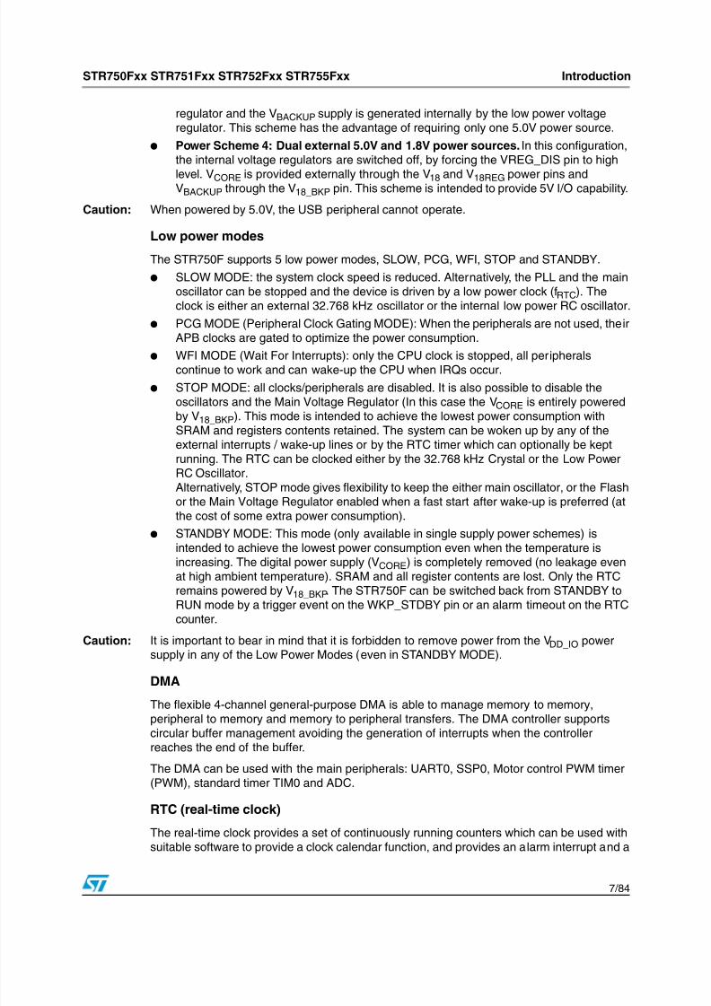
Low power modes
The STR750F supports 5 low power modes, SLOW, PCG, WFI, STOP and STANDBY.
● SLOW MODE: the system clock speed is reduced. Alternatively, the PLL and the mainoscillator can be stopped and the device is driven by a low power clock (fRTC). Theclock is either an external 32.768 kHz oscillator or the internal low power RC oscillator.
● PCG MODE (Peripheral Clock Gating MODE): When the peripherals are not used, theirAPB clocks are gated to optimize the power consumption.
● WFI MODE (Wait For Interrupts): only the CPU clock is stopped, all peripheralscontinue to work and can wake-up the CPU when IRQs occur.
● STOP MODE: all clocks/peripherals are disabled. It is also possible to disable theoscillators and the Main Voltage Regulator (In this case the VCORE is entirely poweredby V18_BKP). This mode is intended to achieve the lowest power consumption withSRAM and registers contents retained. The system can be woken up by any of theexternal interrupts / wake-up lines or by the RTC timer which can optionally be keptrunning. The RTC can be clocked either by the 32.768 kHz Crystal or the Low PowerRC Oscillator.Alternatively, STOP mode gives flexibility to keep the either main oscillator, or the Flashor the Main Voltage Regulator enabled when a fast start after wake-up is preferred (atthe cost of some extra power consumption).
● STANDBY MODE: This mode (only available in single supply power schemes) isintended to achieve the lowest power consumption even when the temperature isincreasing. The digital power supply (VCORE) is completely removed (no leakage evenat high ambient temperature). SRAM and all register contents are lost. Only the RTCremains powered by V18_BKP. The STR750F can be switched back from STANDBY toRUN mode by a trigger event on the WKP_STDBY pin or an alarm timeout on the RTCcounter.
Caution: It is important to bear in mind that it is forbidden to remove power from the VDD_IO powersupply in any of the Low Power Modes (even in STANDBY MODE).
DMA
The flexible 4-channel general-purpose DMA is able to manage memory to memory,peripheral to memory and memory to peripheral transfers. The DMA controller supportscircular buffer management avoiding the generation of interrupts when the controllerreaches the end of the buffer.
The DMA can be used with the main peripherals: UART0, SSP0, Motor control PWM timer(PWM), standard timer TIM0 and ADC.
RTC (real-time clock)
The real-time clock provides a set of continuously running counters which can be used withsuitable software to provide a clock calendar function, and provides an alarm interrupt and a

8/8/2019 11260
http://slidepdf.com/reader/full/11260 8/84
Introduction STR750Fxx STR751Fxx STR752Fxx STR755Fxx
8/ 84
periodic interrupt. It is clocked by an external 32.768 kHz oscillator or the internal low powerRC oscillator. The RC has a typical frequency of 300 kHz and can be calibrated.
WDG (watchdog timer)
The watchdog timer is based on a 16-bit downcounter and 8-bit prescaler. It can be used aswatchdog to reset the device when a problem occurs, or as free running timer for applicationtime out management.
Timebase timer (TB)
The timebase timer is based on a 16-bit auto-reload counter and not connected to the I/Opins. It can be used for software triggering, or to implement the scheduler of a real-timeoperating system.
Synchronizable standard timers (TIM2:0)
The three standard timers are based on a 16-bit auto-reload counter and feature up to 2
input captures and 2 output compares (for external triggering or time base / time outmanagement). They can work together with the PWM timer via the Timer Link feature forsynchronization or event chaining. In reset state, timer Alternate Function I/Os areconnected to the sameI/O ports in both 64-pin and 100-pin devices. To optimize timer functions in 64-pin devices,timer Alternate Function I/Os can be connected, or “remapped”, to other I/O ports assummarized in Table 3 and detailed in Table 6 . This remapping is done by the application viaa control register.
Any of the standard timers can be used to generate PWM outputs. One timer (TIM0) is
mapped to a DMA channel.
Motor control PWM timer (PWM)
The Motor Control PWM Timer (PWM) can be seen as a three-phase PWM multiplexed on 6channels. The 16-bit PWM generator has full modulation capability (0...100%), edge orcentre-aligned patterns and supports dead-time insertion. It has many features in commonwith the standard TIM timers which has the same architecture and it can work together withthe TIM timers via the Timer Link feature for synchronization or event chaining.The PWMtimer is mapped to a DMA channel.
Table 3. Standard timer alternate function I/Os
Standard timer functions
Number of alternate function I/Os
100-pinpackage
64-pin package
Default mapping Remapped
TIM 0Input Capture 2 1 2
Output Compare/PWM 2 1 2
TIM 1Input Capture 2 1 1
Output Compare/PWM 2 1 1
TIM 2Input Capture 2 2 2
Output Compare/PWM 2 1 2

8/8/2019 11260
http://slidepdf.com/reader/full/11260 9/84
STR750Fxx STR751Fxx STR752Fxx STR755Fxx Introduction
9/ 84
I²C bus
The I²C bus interface can operate in multi-master and slave mode. It can support standardand fast modes (up to 400KHz).
High speed universal asynch. receiver transmitter (UART)
The three UART interfaces are able to communicate at speeds of up to 2 Mbit/s. Theyprovide hardware management of the CTS and RTS signals and have LIN Master capability.
To optimize the data transfer between the processor and the peripheral, two FIFOs(receive/transmit) of 16 bytes each have been implemented.
One UART can be served by the DMA controller (UART0).
Synchronous serial peripheral (SSP)
The two SSPs are able to communicate up to 8 Mbit/s (SSP1) or up to 16 Mbit/s (SSP0) instandard full duplex 4-pin interface mode as a master device or up to 2.66 Mbit/s as a slave
device. To optimize the data transfer between the processor and the peripheral, two FIFOs(receive/transmit) of 8 x 16 bit words have been implemented. The SSPs support theMotorola SPI or TI SSI protocols.
One SSP can be served by the DMA controller (SSP0).
Controller area network (CAN)
The CAN is compliant with the specification 2.0 part B (active) with a bit rate up to 1Mbit/s. Itcan receive and transmit standard frames with 11-bit identifiers as well as extended frameswith 29-bit identifiers. Up to 32 message objects are handled through an internal RAMbuffer. In LQFP64 devices, CAN and USB cannot be connected simultaneously.
Universal serial bus (USB)
The STR750F embeds a USB device peripheral compatible with the USB Full speed 12Mbs.The USB interface implements a full speed (12 Mbit/s) function interface. It has softwareconfigurable endpoint setting and suspend/resume support. The dedicated 48 MHz clocksource is generated from the internal main PLL. VDD must be in the range 3.3V±10% forUSB operation.
ADC (analog to digital converter)
The 10-bit Analog to Digital Converter, converts up to 16 external channels (11 channels in64-pin devices) in single-shot or scan modes. In scan mode, continuous conversion isperformed on a selected group of analog inputs. The minimum conversion time is 3.75 µs(including the sampling time).
The ADC can be served by the DMA controller.
An analog watchdog feature allows you to very precisely monitor the converted voltage of upto four channels. An IRQ is generated when the converted voltage is outside theprogrammed thresholds.
The events generated by TIM0, TIM2 and PWM timers can be internally connected to theADC start tr igger, injection trigger, and DMA trigger respectively, to allow the application tosynchronize A/D conversion and timers.

8/8/2019 11260
http://slidepdf.com/reader/full/11260 10/84
Introduction STR750Fxx STR751Fxx STR752Fxx STR755Fxx
10/84
GPIOs (general purpose input/output)
Each of the 72 GPIO pins (38 GPIOs in 64-pin devices) can be configured by software asoutput (push-pull or open-drain), as input (with or without pull-up or pull-down) or asPeripheral Alternate Function. Port 1.15 is an exception, it can be used as general-purpose
input only or wake-up from STANDBY mode (WKP_STDBY). Most of the GPIO pins areshared with digital or analog alternate functions.

8/8/2019 11260
http://slidepdf.com/reader/full/11260 11/84
STR750Fxx STR751Fxx STR752Fxx STR755Fxx Introduction
11/ 84
3.2 Block diagram
Figure 1. STR750 block diagram
P0[31:0]
EXT.IT
WATCHDOG
NESTED
10-bit ADC
JTAG & ICE-RT
ARM7TDMI-S
16AF
JTDIJTCKJTMS
NJTRST
JTDO
NRSTINNRSTOUT
V18
VDD_IO
15AF
VDDA_ADCVSSA_ADC
P1[19:0]
APBBRIDGE
USB Full SpeedUSBDPUSBDM
MOSI,MISO,
UART0
RX,TX,CTS,
SERIAL MEMORY
SRAM 16KB
RX,TX,CTS,FIFO2x(16x8bit)
UART1FIFO
2x(16x8bit)
SSP1FIFO2x(8x16bit)
WAKEUP
4 CS as AF
GPIO PORT 0
GPIO PORT 1
60MHz
V18BKP
MOSI,MISO,SSP0FIFO2x(8x16bit)
SCL,SDAI2C
RX,TX,CTS,UART2FIFO2x(16x8bit)
TEST
GP DMA
2xICAP, 2xOCMP
2xICAP, 2xOCMP
2xICAP, 2xOCMP
XT1XT2
RTC_XT1RTC_XT2
PLL
APB (up to 32 MHz)
VDDA_PLLVSSA_PLL
CK_USB
CK_RTC
as AF
as AF
as AF
as AF
RTS as AF
RTS as AF
as AF
as AF
as AF
FLASH 256KB
DC-DC3.3V TO 1.8V
VCORE
VDD_IO
RESET &POWER
MAINVSS
RTC
as AF
Arbiter
PWM1, PWM1NPWM2, PWM2NPWM3, PWM3N
PWM_EMERGENCYas AF
+16KB (RWW)
SCLK, MOSIMISO as AF
4 streams B U S M A T R I X
A H B L I T E ( u p t o 6 0 M H z )
CPU
INTERFACE
P2[19:0] GPIO PORT 2
AF: alternate function on I/O port pin
Note: I/Os shown for 100 pin devices. 64-pin devices have the I/O set shown in Figure 3 .
CAN 2.0BRX,TXas AF
SCK,NSS
SCK,NSS
TB TIMER
RTS
TIM0 TIMER
TIM1 TIMER
TIM2 TIMER
PWM TIMER
CK_SYS
AHB
AHB
INTERRUPTCTL
OSC
32xIRQ
2xFIQ
VBACKUP
VDDA_ADC
VDDA_PLL
LOW POWER
HRESETN
PRESETN
PCLK
HCLK
4M
OSC32K
LPOSC
FREEOSC
CLOCKMANAGE-
MENT
BOOT0
BOOT1,
as AF

8/8/2019 11260
http://slidepdf.com/reader/full/11260 12/84
Pin description STR750Fxx STR751Fxx STR752Fxx STR755Fxx
12/ 84
4 Pin description
Figure 2. LQFP100 pinout
1 0
0
9 9 9 8 9 7 9 6 9 5 9 4 9 3 9 2 9 1 9 0 8 9 8 8 8 7 8 6 8 5 8 4 8 3 8 2 8 1 8 0 7 9 7 8 7 7 7 61234567891011121314151617181920
2122232425
7574737271706968676665646362616059585756
5554535251
ADC_IN13 / P1.12ADC_IN0 / TIM2_OC1/ P0.02
MCO / TIM0_TI1 / P0.01BOOT0 / TIM0_OC1 / P0.00
TIM1_TI2 / P0.31TIM1_OC2 / P0.30
ADC_IN8 / TIM1_TI1 / P0.29TIM1_OC1 / P0.28
TESTVSS_IO
ADC_IN6 / UART1_RTS / P0.23TIM2_OC1/ P2.04
UART1_RTS / P2.03P2.02
ADC_IN5 / UART1_CTS / P0.22UART1_TX / P0.21UART1_RX / P0.20
JTMS / P1.19JTCK / P1.18JTDO / P1.17
JTDI / P1.16NJTRST
P2.01P2.00
UART0_RTS / RTCK / P0.13
VREG_DISVSS_IOVSSA_ADCP2.10P2.11VDDA_ADCVDD_IOP1.02 / TIM2_OC2P1.03 / TIM2_TI2USB_DPUSB_DNP0.14 / CAN_RXP0.15 / CAN_TXP2.12P2.13P1.15 / WKP_STDBYNRSTINNRSTOUTXRTC2XRTC1
V18BKPVSSBKPVSS18V18REGP2.14
S M I_ C S
1 / A D C_
I N 2 / U A R T 0_
C T S / P 0 . 1 2
S M I_
C S 2 / B O O T 1 / U A R T 0_
T X / P 0 . 1 1
S M I_ C S 3 / U A R T 0_
R X / P 0 . 1 0
I 2 C_
S D A / P 0 . 0 9
I 2 C_
S C L / P 0 . 0 8
P 2 . 1 9
P 2 . 1 8
U A R T 2_
R T S / P 2 . 1 7
A D C_
I N 1 2 / U A R T 0_
R T S P 1 . 1 1
A D C_
I N 7 / U A R T 2_
R T S / P 0 . 2 7
U A R T 2_
C T S / P 0 . 2 6
U A R T 2_
T X / P 0 . 2 5
U A R T 2_
R X / P 0 . 2 4
A D C_ I N 4 / S S P 1_
N S S / U S B_
C K / P 0 . 1 9
S S P 1_
M O S I / P 0 . 1 8
A D C_
I N 3 / S S P 1_
M I S O / P 0 . 1 7
S S P 1_
S C L K / P 0 . 1 6
P 2 . 1 6
V D D_
I O
V D D A_
P L L
X T 2
X T 1
V S S_
I O
V S S A_
P L L
P 2 . 1 5
P 0 . 0 3 / T I M 2_
T I 1 / A D C_
I N 1
V D D_
I O
V S S_
I O
V S S 1 8
V 1 8
P 1 . 0 0 / T I M 0_
O C 2
P 1 . 0 1 / T I M 0_
T I 2
P 1 . 1 3 / A D C_
I N 1 4
P 1 . 1 4 / A D C_
I N 1 5
P 1 . 0 4 / P W M 3 N / A D C_
I N 9
P 1 . 0 5 / P W M 3
P 1 . 0 6 / P W M 2 N / A D C_
I N 1 0
P 1 . 0 7 / P W M 2
P 1 . 0 8 / P W M 1 N / A D C_
I N 1 1
P 2 . 0 5 / P W M 3 N
P 2 . 0 6 / P W M 3
P 2 . 0 7 / P W M 2 N
P 2 . 0 8 / P W M 2
P 2 . 0 9 / P W M 1 N
P 1 . 0 9 / P W M 1
P 1 . 1 0 / P W M_
E M E R G E N C Y
P 0 . 0 4 / S M I_ C S 0 / S S P 0_
N S S
P 0 . 0 5 / S S P 0_
S C L K / S M I_ C K
P 0 . 0 6 / S M I_ D I N / S S P 0_
M I S O
P 0 . 0 7 / S M I_ D O U T / S S P 0_
M O S I
LQFP100
2 6 2 7 2 8 2 9 3 0 3 1 3 2 3 3 3 4 3 5 3 6 3 7 3 8 3 9 4 0 4 1 4 2 4 3 4 4 4 5 4 6 4 7 4 8 4 9 5 0
V18BKP I/Os
= 16 A/D input channels= 15 External interrupts / Wake-up Lines

8/8/2019 11260
http://slidepdf.com/reader/full/11260 13/84
STR750Fxx STR751Fxx STR752Fxx STR755Fxx Pin description
13/ 84
Figure 3. LQFP64 pinout
I 2 C_
S C
L / P 0 . 0 8
A D C_
I N 1 2 / U A R T 0_
R T
S / P 1 . 1 1
A D C_
I N 4 / S S P 1_
N S S / U S B_ C
K / P 0 . 1 9
S S P 1_
M O S I / P 0 . 1 8
A D C_
I N 3 / S S P 1_
M I S
O / P 0 . 1 7
S S P 1_
S C L
K / P 0 . 1 6
V D D_
I O_
3
V D D A_
P L L
X T 2
X T 1
V S S_
I O_
3
V S S A_
P L L
S M I_ C S 1 / A D C_
I N 2 / U A R T 0_
C T S / U A R T 2_ R X / P 0 . 1 2
S M I_ C S 2 / B O O T 1 / U A R T 0_ T
X / P 0 . 1 1
S M I_ C S 3 / U A R T 0_ R
X / P 0 . 1 0
I 2 C_ S
D A / P 0 . 0 9
64 63 62 61 60 59 58 57 56 55 54 53 52 51 50 4948
47
46
45
44
43
42
41
40
39
38
37
36
35
34
3317 18 19 20 21 22 23 24 29 30 31 3225 26 27 28
1
2
3
4
5
6
7
8
9
10
11
12
13
14
15
16
ADC_IN8 / TIM1_TI1 / P0.29
TIM1_OC1 / P0.28
TEST
VSS_IO_4
UART1_TX / P0.21
UART1_RX / P0.20
JTMS / P1.19
JTCK / P1.18
JTDO / P1.17JTDI / P1.16
NJTRST
UART2_TX / UART0_RTS / RTCK / P0.13
ADC_IN13 / P1.12
ADC_IN0 / TIM2_OC1 / P0.02
MCO / TIM0_TI1 / P0.01
BOOT0 / TIM0_OC1 / P0.00
VDD_IO_2
P1.03 / TIM2_TI2
P0.14 / CAN_RX or USB_DP
P0.15 / CAN_TX or USB_DN
NRSTIN
NRSTOUT
XRTC2
XRTC1
V18BKPVSSBKP
VSS18
V18REG
VREG_DIS
VSS_IO_2
VSSA_ADC
VDDA_ADC
V 1 8
P 1 . 0 4 / P W M 3 N / A D C_
I N 9
P 1 . 0 5 / P W M 3
P 1 . 0 6 / P W M 2 N / A D C_
I N 1 0
P 1 . 0 7 / P W M 2
P 1 . 0 8 / P W M 1 N / A D C_
I N 1 1
P 1 . 0 9 / P W M 1
P 1 . 1 0 / P W M_
E M E R G E N C Y
P 0 . 0 4 / S M I_ C S 0 / S S P 0_
N S S
P 0 . 0 5 / S S P 0_
S C L K / S M I_ C K
P 0 . 0 6 / S M I_ D I N / S S P 0_
M I S O
P 0 . 0 7 / S M I_ D O U T / S S P 0_
M O S
I
P 0 . 0 3 / T I M 2_
T I 1 / A D C_
I N 1
V D D_
I O_
1
V S S_
I O_
1
V S S 1 8
LQFP64
= 11 A/D input channels= 13 External interrupts / Wake-up Lines
V18BKP I/Os

8/8/2019 11260
http://slidepdf.com/reader/full/11260 14/84
Pin description STR750Fxx STR751Fxx STR752Fxx STR755Fxx
14/ 84
Table 4. LFBGA100 ball connections
1 2 3 4 5 6 7 8 9 10
A P0.03 P1.13 P1.14 P1.04 P1.06 P1.08 P0.05 P0.06 P0.07 P1.02
B P1.12 P0.02 P0.01 P1.05 P1.07 P1.09 P0.04 P2.13 P1.03 P2.10
C P0.31 P0.00 VDD_IO V18 P1.10 P2.09 VSS_IO VSSA_ADC P2.11 USB_DP
D P0.29 P0.30 VSS_IO VSS18 P1.01 P1.15 VDD_IO VDDA_ADC P2.12 USB_DN
E P0.28 P0.23 P0.22 VSS_IO TEST P1.00 NRSTOUT VREG_DIS NRSTIN P0.14
F P2.03 P0.21 P0.20 P2.02 P2.04 P2.05 P2.06 VSS18 VSSBKP P0.15
G NJTRST P1.18 P1.19 P2.01 P2.00 P2.07 2.08 V18REG V18BKP XRTC2
H P0.13 P1.16 P1.17 P2.19 P2.18 P2.17 P0.24 P2.14 P2.16 XRTC1
J P0.11 P0.12 P1.11 P0.27 P0.19 P0.26 P0.25 P2.15 VDD_IO VSS_IO
K P0.10 P0.09 P0.08 P0.18 P0.17 P0.16 XT1 XT2 VDDA_PLL VSSA_PLL
Table 5. LFBGA64 ball connections
1 2 3 4 5 6 7 8
A P0.03 VSS_IO P1.04 P1.06 P1.08 P0.05 P0.06 P0.07
B P1.12 VDD_IO P1.05 P1.07 P1.09 P0.04 P1.10 P1.03
C P0.01 P0.02 P0.00 V18 VSS18 VDD_IO VSS_IO P0.14
D P0.29 P0.28 TEST VSS_IO VREG_DIS VDDA_ADC VSSA_ADC P0.15
E P1.18 P1.19 P0.20 P0.21 NRSTOUT NRSTIN V18BKP XRTC2
F P0.13 NJTRST P1.16 P1.17 V18REG VSS18 VSSBKP XRTC1
G P0.11 P0.12 P1.11 P0.19 VDD_IO VSS_IO VDDA_PLL VSSA_PLL
H P0.10 P0.09 P0.08 P0.17 P0.18 P0.16 XT2 XT1

8/8/2019 11260
http://slidepdf.com/reader/full/11260 15/84
STR750Fxx STR751Fxx STR752Fxx STR755Fxx Pin description
15/ 84
4.1 Pin description table
Legend / abbreviations for Table 6 :
Type: I = input, O = output, S = supply,
Input levels: All Inputs are LVTTL at VDD_IO = 3.3V+/-0.3V or TTLat VDD_IO = 5V± 0.5V. In both cases, TT meansVILmax =0.8V VIHmin=2.0V
Inputs: All inputs can be configured as floating or withinternal weak pull-up or pull down (pu/pd)
Outputs: All Outputs can be configured as Open Drain (OD) orPush-Pull (PP) (see also note 6 below Table 6 ).There are 3 different types of Output with differentdrives and speed characteristics:
– O8: fmax = 40 MHz on CL=50pF and 8 mA staticdrive capability for VOL=0.4V and up to 20 mA forVOL=1.3V (seeOutput driving current on page 55 )
– O4: fmax = 20 MHz on CL=50pF and 4 mA staticdrive capability for VOL=0.4V (seeOutput driving current on page 55 )
– O2: fmax = 10 MHz on CL=50pF and 2 mA staticdrive capability of for VOL=0.4V (seeOutput driving current on page 55 )
External interrupts/wake-up lines: EITx

8/8/2019 11260
http://slidepdf.com/reader/full/11260 16/84
Pin description STR750Fxx STR751Fxx STR752Fxx STR755Fxx
16/ 84
Port reset state
The reset state of the I/O ports is GPIO input floating. Exceptions are P1[19:16] and P0.13which are configured as JTAG alternate functions:
● The JTAG inputs (JTDI, JTMS and JTDI) are configured as input floating and are readyto accept JTAG sequences.
● The JTAG output JTDO is configured as floating when idle (no JTAG operation) and isconfigured in output push-pull only when serial JTAG data must be output.
● The JTAG output RTCK is always configured as output push-pull. It outputs '0' levelduring the reset phase and then outputs the JTCK input signal resynchronized 3 timesby the internal AHB clock.
● The GPIO_PCx registers do not control JTAG AF selection, so the reset values ofGPIO_PCx for P1[19:16] and P0. 13 are the same as other ports. Refer to the GPIOsection of the STR750 Reference Manual for the register description and reset values.
● P0.11 and P0.00 are sampled by the boot logic after reset, prior to fetching the firstword of user code at address 0000 0000h.
● When booting from SMI (and only in this case), the reset state of the following GPIOs is"SMI alternate function output enabled":
– P0.07 (SMI_DOUT)
– P0.05 (SMI_CLK)
– P0.04 (SMI_CS0)
– P0.06 (SMI_DIN)
Note that the other SMI pins: SMI_CS1,2,3 (P0.12, P0.11, P0.10) are not affected.
To avoid excess power consumption, unused I/O ports must be tied to ground.
Table 6. STR750F pin description
Pin n°
Pin name T y p e
Input Output
U s a b l e i n S t a n d b y
Main
function
(after
reset)
Alternate function
L Q F P 1 0 0 ( 1 )
L F B G A 1 0 0 ( 1 )
L Q F P 6 4 ( 2 )
L F B G A 6 4 ( 2 )
I n p u t L e v e l
f l o a t i n g
p u / p d
E x t . i n t / W a k e - u p
C a p a b i l i t y
OD(3) PP
1 B1 1 B1P1.12 / ADC_IN13
I/O TT X X EIT12 O8 X X Port 1.12ADC: Analoginput 13
2 B2 2 C2P0.02 / TIM2_OC1 / ADC_IN0
I/O TT X X EIT0 O8 X X Port 0.02TIM2: Output Compare 1(4)
ADC: Analoginput 0
3 B3 3 C1P0.01 / TIM0_TI1
/ MCOI/O TT X X O8 X X Port 0.01
TIM0: InputCapture / trigger
/ external clock 1
Main ClockOutput
4 C2 4 C3P0.00 / TIM0_OC1 / BOOT0
I/O TT X X O8 X X
Port 0.00 / Boot modeselectioninput 0
TIM0: Output Compare 1
5 C1 P0.31 / TIM1_TI2 I/O TT X X O2 X X Port 0.31TIM1: Input Capture / trigger / external clock 2
6 D2P0.30 / TIM1_OC2
I/O TT X X O2 X X Port 0.30 TIM1: Output Compare 2

8/8/2019 11260
http://slidepdf.com/reader/full/11260 17/84
STR750Fxx STR751Fxx STR752Fxx STR755Fxx Pin description
17/ 84
7 D1 5 D1P0.29 / TIM1_TI1
/ ADC_IN8I/O TT X X O2 X X Port 0.29
TIM1: InputCapture 1
ADC: Analoginput 8
8 E1 6 D2P0.28 / TIM1_OC1
I/O TT X X O2 X X Port 0.28 TIM1: Output Compare 1
9 E5 7 D3 TEST I Reserved, must be tied to ground
10 E4 8 D4 VSS_IO S Ground Voltage for digital I/Os
11 E2
P0.23 /
UART1_RTS / ADC_IN6
I/O TT X X O2 X X Port 0.23
UART1: Ready
To Sendoutput(4)
ADC analog input6
12 F5P2.04 / TIM2_OC1
I/O TT X X O2 X X Port 2.04TIM2: Output Compare 1(4)
13 F1P2.03 / UART1_RTS
I/O TT X X O2 X X Port 2.03UART1: ReadyTo Send output(4)
14 F4 P2.02 I/O TT X X O2 X X Port 2.02
15 E3P0.22 /
UART1_CTS / ADC_IN5
I/O TT X X O2 X X Port 0.22UART1: Clear ToSend input
ADC: Analoginput 5
16 F2 9 E4P0.21 / UART1_TX
I/O TT X X O2 X X Port 0.21UART1: Transmit data output(remappable to P0.15)(4)
17 F3 10 E3 P0.20 / UART1_RX I/O TT X X O2 X X Port 0.20 UART1: Receive data input(remappable to P0.14)(4)
18 G3 11 E2 P1.19 / JTMS I/O TT X X O2 X XJTAG modeselectioninput(6)
Port 1.19
19 G2 12 E1 P1.18 / JTCK I/O TT X X O2 X XJTAG clock input(6) Port 1.18
20 H3 13 F4 P1.17 / JTDO I/O TT X X O8 X XJTAG dataoutput(6) Port 1.17
21 H2 14 F3 P1.16 / JTDI I/O TT X X O2 X XJTAG datainput(6) Port 1.16
22 G1 15 F2 NJTRST I TT JTAG reset input(5)
23 G4 P2.01 I/O TT X X O2 X X Port 2.01
24 G5 P2.00 I/O TT X X O2 X X Port 2.00
25 H1 16 F1P0.13 / RTCK / UART0_RTSUART2_TX
I/O TT X X O8 X X
JTAGreturnclock output(6)
Port 0.13
UART0: ReadyTo Send output(4)
UART2: Transmit
Data output
(when
remapped)(8)
Table 6. STR750F pin description (continued)
Pin n°
Pin name T y p e
Input Output
U s a b l e i n S
t a n d b y
Main
function(after
reset)
Alternate function
L Q F P 1 0 0 ( 1 )
L F B G A 1 0 0 ( 1 )
L Q F P 6 4 ( 2
)
L F B G A 6 4 (
2 )
I n p u t L e v e l
f l o a t i n g
p u / p d
E x t . i n t / W a k e
- u p
C a p a b i l i t y
OD(3) PP

8/8/2019 11260
http://slidepdf.com/reader/full/11260 18/84
Pin description STR750Fxx STR751Fxx STR752Fxx STR755Fxx
18/ 84
26 J2 17 G2
P0.12 / UART2_RX / UART0_CTS / ADC_IN2 / SMI_CS1
I/O TT X X O4 X X Port 0.12
UART0: Clear ToSend input
ADC: Analoginput 2
Serial MemoryInterface: chipselect output 1
UART2: Receive
Data input (when
remapped)(8)
27 J1 18 G1
P0.11 / UART0_TX /
BOOT1 / SMI_CS2
I/O TT X X O4 X X
Port0.11/Bootmode
selectioninput 1
UART0: Transmit
data output
Serial MemoryInterface: chip
select output 2
28 K1 19 H1P0.10 / UART0_RX / SMI_CS3
I/O TT X X EIT4 O2 X X Port 0.10UART0: ReceiveData input
Serial MemoryInterface: chipselect output 3
29 K2 20 H2 P0.09 / I2C_SDA I/O TT X X O4 X X Port 0.09 I2C: Serial Data
30 K3 21 H3 P0.08 / I2C_SCL I/O TT X X EIT3 O4 X X Port 0.08 I2C: Serial clock
31 H4 P2.19 I/O TT X X O2 X X Port 2.19
32 H5 P2.18 I/O TT X X O2 X X Port 2.18
33 H6P2.17 / UART2_RTS
I/O TT X X O2 X X Port 2.17 UART2: Ready To Send output(4)
34 J3 22 G3
P1.11
/UART0_RTSADC_IN12 I/O TT X X EIT11 O8 X X Port 1.11
UART0: Ready
To Send output(4)
ADC: Analog
input 12
35 J4P0.27 / UART2_RTS / ADC_IN7
I/O TT X X O2 X X Port 0.27UART2: ReadyTo Send output(8)
ADC: Analoginput 7
36 J6P0.26 / UART2_CTS
I/O TT X X O2 X X Port 0.26 UART2: Clear To Send input
37 J7P0.25 / UART2_TX
I/O TT X X O2 X X Port 0.25UART2: Transmit data output(remappable to P0.13)(8)
38 H7P0.24 / UART2_RX
I/O TT X X O2 X X Port 0.24UART2: Receive data input(remappable to P0.12)(8)
39 J5 23 G4
P0.19 / USB_CK /
SSP1_NSS / ADC_IN4
I/O TT X X EIT6 O2 X X Port 0.19
SSP1: Slaveselect input(remappable to
P0.11)
(8)
ADC: Analoginput 4
USB:48 MHz Clockinput
40 K4 24 H5P0.18 / SSP1_MOSI
I/O TT X X O2 X X Port 0.18SSP1: Master out/slave in data(remappable to P0.10)(8)
41 K5 25 H4P0.17 / SSP1_MISO / ADC_IN3
I/O TT X X O2 X X Port 0.17
SSP1: Masterin/slave out data(remappable toP0.09)(8)
ADC: Analoginput 3
42 K6 26 H6P0.16 / SSP1_SCLK
I/O TT X X O2 X X Port 0.16SSP1: serial clock (remappable toP0.08)(8)
Table 6. STR750F pin description (continued)
Pin n°
Pin name T y p e
Input Output
U s a b l e i n S
t a n d b y
Main
function(after
reset)
Alternate function
L Q F P 1 0 0 ( 1 )
L F B G A 1 0 0 ( 1 )
L Q F P 6 4 ( 2
)
L F B G A 6 4 (
2 )
I n p u t L e v e l
f l o a t i n g
p u / p d
E x t . i n t / W a k e
- u p
C a p a b i l i t y
OD(3) PP

8/8/2019 11260
http://slidepdf.com/reader/full/11260 19/84
STR750Fxx STR751Fxx STR752Fxx STR755Fxx Pin description
19/ 84
43 H9 P2.16 I/O TT X X O2 X X Port 2.16
44 J9 27 G5 VDD_IO S Supply voltage for digital I/Os
45 K9 28 G7 VDDA_PLL S Supply voltage for PLL
46 K8 29 H7 XT24 MHz main oscillator
47 K7 30 H8 XT1
48 J10 31 G6 VSS_IO S Ground voltage for digital I/Os
49 K10 32 G8 VSSA_PLL S Ground voltage for PLL
50 J8 P2.15 I/O TT X X O2 X X Port 2.15
51 H8 P2.14 I/O TT X X O2 X X Port 2.14
52 G8 33 F5 V18REG S
Stabilization for main voltage regulator. Requiresexternal capacitors of at least 10µF betweenV18REG and VSS18. See Figure 4.2 .
To be connected to the 1.8V external power supplywhen embedded regulators are not used,
53 F8 34 F6 VSS18 S Ground Voltage for the main voltage regulator
54 F9 35 F7 VSSBKP S Stabilization for low power voltage regulator.
55 G9 36 E7 V18BKP S
Ground Voltage for the low power voltage regulator.Requires external capacitors of at least 1µF
between V18BKP and VSSBKP. See Figure 4.2 .To be connected to the 1.8V external power supplywhen embedded regulators are not used,
56 H10 37 F8 XRTC1 X32 kHz oscillator for Realtime Clock
57 G10 38 E8 XRTC2 X
58 E7 39 E5 NRSTOUT O X Reset output
59 E9 40 E6 NRSTIN I TT X Reset input
60 D6P1.15 / WKP_STDBY
I TT X EIT15 X Port 1.15 Wake-up from STANDBY input pin
61 B8 P2.13 I/O TT X X O2 X X Port 2.13
62 D9 P2.12 I/O TT X X O2 X X Port 2.12
63 F10
41
(7)
D8
(7) P0.15 / CAN_TX I/O TT X X O2 X X Port 0.15 CAN: Transmit data output
64 E1042(7)
C8(7) P0.14 / CAN_RX I/O TT X X EIT5 O2 X X Port 0.14 CAN: Receive data input
65 D1041(7)
D8(7) USB_DN I/O USB: bidirectional data (data -)
66 C1042(7)
C8(7) USB_DP I/O USB: bidirectional data (data +)
67 B9 43 B8 P1.03 / TIM2_TI2 I/O TT X X O2 X X Port 1.03TIM2: Input Capture / trigger / external clock 2 (remappable toP0.07)(8)
Table 6. STR750F pin description (continued)
Pin n°
Pin name T y p e
Input Output
U s a b l e i n S
t a n d b y
Main
function(after
reset)
Alternate function
L Q F P 1 0 0 ( 1 )
L F B G A 1 0 0 ( 1 )
L Q F P 6 4 ( 2
)
L F B G A 6 4 (
2 )
I n p u t L e v e l
f l o a t i n g
p u / p d
E x t . i n t / W a k e
- u p
C a p a b i l i t y
OD(3) PP

8/8/2019 11260
http://slidepdf.com/reader/full/11260 20/84
Pin description STR750Fxx STR751Fxx STR752Fxx STR755Fxx
20/ 84
68 A10P1.02 / TIM2_OC2
I/O TT X X O2 X X Port 1.02TIM2: Output compare 2 (remappable to P0.06)(8)
69 D7 44 C6 VDD_IO S Supply Voltage for digital I/Os
70 D8 45 D6 VDDA_ADC S Supply Voltage for A/D converter
71 C9 P2.11 I/O TT X X O2 X X Port 2.11
72 B10 P2.10 I/O TT X X O2 X X Port 2.10
73 C8 46 D7 VSSA_ADC S Ground Voltage for A/D converter
74 C7 47 C7 VSS_IO S Ground Voltage for digital I/Os
75 E8 48 D5 VREG_DIS I TT Voltage Regulator Disable input
76 A9 49 A8P0.07 / SMI_DOUT / SSP0_MOSI
I/O TT X X EIT2 O4 X X Port 0.07Serial MemoryInterface: dataoutput
SSP0: Master outSlave in data
77 A8 50 A7P0.06 / SMI_DIN
/ SSP0_MISOI/O TT X X O4 X X Port 0.06
Serial MemoryInterface: datainput
SSP0: Master inSlave out data
78 A7 51 A6P0.05 / SSP0_SCLK / SMI_CK
I/O TT X X EIT1 O4 X X Port 0.05SSP0: Serialclock
Serial MemoryInterface: Serialclock output
79 B7 52 B6P0.04 / SMI_CS0
/ SSP0_NSSI/O T
TX X O4 X X Port 0.04
Serial MemoryInterface: chipselect output 0
SSP0: Slave
select input
80 C5 53 B7P1.10PWM_EMERGENCY
I/O TT X X EIT10 O2 X X Port 1.10 PWM: Emergency input
81 B6 54 B5 P1.09 / PWM1 I/O TT X X EIT9 O4 X X Port 1.09 PWM: PWM1 output
82 C6 P2.09 / PWM1N I/O TT X X O2 X X Port 2.09PWM: PWM1 complementaryoutput(4)
83 G7 P2.08 / PWM2 I/O TT X X O2 X X Port 2.08 PWM: PWM2 output(4)
84 G6 P2.07 / PWM2N I/O TT X X O2 X X Port 2.07PWM: PWM2 complementaryoutput(4)
85 F7 P2.06 / PWM3 I/O TT X X O2 X X Port 2.06 PWM: PWM3 output(4)
86 F6 P2.05 / PWM3N I/O TT X X O2 X X Port 2.05
PWM: PWM3 complementary
output(4)
87 A6 55 A5P1.08 / PWM1N / ADC_IN11
I/O TT X X O4 X X Port 1.08PWM: PWM1complementaryoutput(8)
ADC: analoginput 11
88 B5 56 B4 P1.07 / PWM2 I/O TT X X EIT8 O4 X X Port 1.07 PWM: PWM2 output(4)
89 A5 57 A4P1.06 / PWM2N / ADC_IN10
I/O TT X X O4 X X Port 1.06PWM: PWM2complementaryoutput(4)
ADC: analoginput 10
90 B4 58 B3 P1.05 / PWM3 I/O TT X X EIT7 O4 X X Port 1.05 PWM: PWM3 output(4)
Table 6. STR750F pin description (continued)
Pin n°
Pin name T y p e
Input Output
U s a b l e i n S
t a n d b y
Main
function(after
reset)
Alternate function
L Q F P 1 0 0 ( 1 )
L F B G A 1 0 0 ( 1 )
L Q F P 6 4 ( 2
)
L F B G A 6 4 (
2 )
I n p u t L e v e l
f l o a t i n g
p u / p d
E x t . i n t / W a k e
- u p
C a p a b i l i t y
OD(3) PP

8/8/2019 11260
http://slidepdf.com/reader/full/11260 21/84
STR750Fxx STR751Fxx STR752Fxx STR755Fxx Pin description
21/ 84
91 A4 59 A3P1.04 / PWM3N / ADC_IN9
I/O TT X X O4 X X Port 1.04PWM: PWM3complementaryoutput(4)
ADC: analoginput 9
92 A3P1.14 / ADC_IN15
I/O TT X X O8 X X Port 1.14 ADC: analog input 15
93 A2P1.13 / ADC_IN14
I/O TT X X EIT13 O8 X X Port 1.13 ADC: analog input 14
94 D5 P1.01 / TIM0_TI2 I/O TT X X O2 X X Port 1.01
TIM0: Input Capture / trigger /
external clock 2 (remappable toP0.05)(8)
95 E6P1.00 / TIM0_OC2
I/O TT X X O2 X X Port 1.00TIM0: Output compare 2 (remappable to P0.04)(8)
96 C4 60 C4 V18 S
Stabilization for main voltage regulator. Requiresexternal capacitors 33nF between V18 and VSS18.See Figure 4.2 .To be connected to the 1.8V external power supplywhen embedded regulators are not used.
97 D4 61 C5 VSS18 S Ground Voltage for the main voltage regulator.
98 D3 62 A2 VSS_IO S Ground Voltage for digital I/Os
99 C3 63 B2 VDD_IO S Supply Voltage for digital I/Os
100 A1 64 A1
P0.03 / TIM2_TI1
/ ADC_IN1 I/O TT X X O2 X X Port 0.03
TIM2: Input
Capture / trigger / external clock 1
ADC: analog
input 1
1. For STR755FVx part numbers, the USB pins must be left unconnected.
2. The non available pins on LQPFP64 and LFBGA64 packages are internally tied to low level.
3. None of the I/Os are True Open Drain: when configured as Open Drain, there is always a protection diode between the I/Opin and VDD_IO.
4. In the 100-pin package, this Alternate Function is duplicated on two ports. You can configure one port to use this AF, theother port is then free for general purpose I/O (GPIO), external interrupt/wake-up lines, or analog input (ADC_IN) wherethese functions are listed in the table.
5. It is mandatory that the NJTRST pin is reset to ground during the power-up phase. It is recommended to connect this pin toNRSTOUT pin (if available) or NRSTIN.
6. After reset, these pins are enabled as JTAG alternate function see (Port reset state on page 16 ). To use these ports asgeneral purpose I/O (GPIO), the DBGOFF control bit in the GPIO_REMAP0R register must be set by software (in this case,debugging these I/Os via JTAG is not possible).
7. There are two different TQFP and BGA 64-pin packages: in the first one, pins 41 and 42 are mapped to USB DN/DP whilefor the second one, they are mapped to P0.15/CAN_TX and P0.14/CAN_RX.
8. For details on remapping these alternate functions, refer to the GPIO_REMAP0R register description.
Table 6. STR750F pin description (continued)
Pin n°
Pin name T y p e
Input Output
U s a b l e i n S
t a n d b y
Main
function(after
reset)
Alternate function
L Q F P 1 0 0 ( 1 )
L F B G A 1 0 0 ( 1 )
L Q F P 6 4 ( 2
)
L F B G A 6 4 (
2 )
I n p u t L e v e l
f l o a t i n g
p u / p d
E x t . i n t / W a k e
- u p
C a p a b i l i t y
OD(3) PP

8/8/2019 11260
http://slidepdf.com/reader/full/11260 22/84
Pin description STR750Fxx STR751Fxx STR752Fxx STR755Fxx
22/ 84
4.2 External components
Figure 4. Required external capacitors when regulators are used
LQFP100LQFP64
52
60
96
33 nF
5310 µF
33 nF
54
551µF 61
V18
V18REG
V18V18BKP
97
VSS18
VSSBKP
44
VDD_IO
1 µF
VSS18
VSS18
33
3410 µF
35
361µF
V18REG
V18BKP
VSS18
VSSBKP
27
VDD_IO
1 µF
LFBGA100
G8
C4
33 nF
F810 µF
F9
G91µF
V18REG
V18V18BKP
D4
VSS18
VSSBKP
J9
VDD_IO
1 µF
VSS18
LFBGA64
C4
33 nF
C5V18
VSS18
F5
F610 µF
F7
E71µF
V18REG
V18BKP
VSS18
VSSBKP
G5
VDD_IO
1 µF

8/8/2019 11260
http://slidepdf.com/reader/full/11260 23/84
STR750Fxx STR751Fxx STR752Fxx STR755Fxx Memory map
23/ 84
5 Memory map
Figure 5. Memory map
Reserved
Addressable Memory Space
0
1
2
3
4
1K
5
6
7
0x1FFF FFFF
0x2000 0000
0x3FFF FFFF
0x4000 0000
0x5FFF FFFF
0x6000 0000
0x7FFF FFFF
0x8000 0000
0x9FFF FFFF0xA000 0000
0xBFFF FFFF
0xC000 0000
0xDFFF FFFF
0xE000 0000
0xFFFF FFFF
0xFFFF 8000
0xFFFF 83FF
0xFFFF 8400
0xFFFF 87FF
0xFFFF 8800
0xFFFF 8BFF
0xFFFF 8C00
0xFFFF 8FFF
0xFFFF 9000
0xFFFF 93FF
0xFFFF 9400
0xFFFF 97FF
0xFFFF 9800
0xFFFF 9BFF
0xFFFF 9C00
0xFFFF 9FFF
0xFFFF A000
0xFFFF A3FF
0xFFFF A800
0xFFFF ABFF
0xFFFF AC00
0xFFFF AFFF
0xFFFF B000
0xFFFF C3FF
0xFFFF C400
0xFFFF C7FF
0xFFFF C800
0xFFFF CBFF
0xFFFF CC00
0xFFFF D000
1K
1K
1K
1K
1K
1K
1K
1K
1K
1K
1K
1K
0x6000 0047
0x0000 0000
Peripheral Memory Space4 Gbytes 32 Kbytes
Boot Memory(1) 128K/256K
CONF + MRCC 1K
APB TO ARM7BRIDGE
0xFFFF 800032K
Reserved
0xFFFF CFFF
Internal SRAM 16K0x4000 3FFF
SMI Ext. Memory0x83FF FFFF
4 x 16M0xFFFF C000
0xFFFF D400
0xFFFF D3FF
0xFFFF D800
0xFFFF D7FF
0xFFFF DC00
0xFFFF DBFF
0xFFFF E000
0xFFFF DFFF
0xFFFF E400
0xFFFF E3FF
0xFFFF E800
0xFFFF E7FF
0xFFFF EC00
0xFFFF EBFF
1K
1K
1K
1K
1K
1K
1K
1K
1K
1K
1K
1K
ADC
TIM0
TIM1
TIM2
PWM
USB Registers
CAN
Reserved
I2C
Reserved
UART0
UART1
UART2
Reserved
RTC
EIC0xFFFF F800
0xFFFF F7FF
0xFFFF F4000xFFFF F3FF
0xFFFF F000
0xFFFF EFFF
0xFFFF B3FF
0xFFFF B400
0xFFFF B7FF
0xFFFF B8001K
0xFFFF BBFF
GPIO I/O Ports
Reserved
DMA
WDG
Reserved
SSP0
SSP1 1K0xFFFF BFFF
0xFFFF BC00
TB Timer
Reserved
FLASH Memory Space
128/256 Kbytes
B0F5
0x2000 1FFF0x2000 0000
0x2000 2000
0x2000 3FFF0x2000 4000
0x2000 5FFF0x2000 6000
0x2000 7FFF
0x2000 8000
0x2000 FFFF
0x2001 0000
0x2001 FFFF
0x2010 0000
0x2010 0017
0x2010 C000
0x2010 DFFF
8K
8K
8K
8K
32K
24B
64K
B0F4
Flash registers
Internal Flash 128K/256K+16K+32B
B0F6(2)
0x2002 0000
0x2002 FFFF
64K
B0F7(2)
0x2003 0000
0x2003 FFFF
64K
Reserved
0xFFFF A200
EXTIT
0x2010 0017
B0F3
B0F2
B0F1
B0F0
1K
1K
1K
0xFFFF A400
0xFFFF A7FF
1K
(1) In internal Flash Boot Mode, internal FLASH is aliased at 0x0000 0000h
(2) Only available in STR750Fx2
8KSystemMemory
0x200C 0000
0x200C 1FFF8K
B1F10x200C 2000
8K
USB RAM 256 x16-bit
Reserved
Reserved
0x9000 00000x9000 0013 SMI Registers 20B
B1F0
0x200C 3FFF
0x200C 4000
0xFFFF FFFF
0xFFFF FC00
0xFFFF FBFF
1KReserved

8/8/2019 11260
http://slidepdf.com/reader/full/11260 24/84
Electrical parameters STR750Fxx STR751Fxx STR752Fxx STR755Fxx
24/ 84
6 Electrical parameters
6.1 Parameter conditions
Unless otherwise specified, all voltages are referred to VSS.
6.1.1 Minimum and maximum values
Unless otherwise specified the minimum and maximum values are guaranteed in the worstconditions of ambient temperature, supply voltage and frequencies by tests in production on100% of the devices with an ambient temperature at TAmax (given by the selectedtemperature range).
Data based on product characterisation, design simulation and/or technology characteristicsare indicated in the table footnotes and are not tested in production. Based oncharacterization, the minimum and maximum values refer to sample tests and represent the
mean value plus or minus three times the standard deviation (mean±3Σ).
6.1.2 Typical values
Unless otherwise specified, typical data are based on TA=25° C, VDD_IO=3.3 V (for the3.0 V≤VDD_IO≤3.6 V voltage range) and V18=1.8 V. They are given only as design guidelinesand are not tested.
Typical ADC accuracy values are determined by characterization of a batch of samples froma standard diffusion lot over the full temperature range, where 95% of the devices have anerror less than or equal to the value indicated (mean±2Σ).
6.1.3 Typical curves
Unless otherwise specified, all typical curves are given only as design guidelines and arenot tested.

8/8/2019 11260
http://slidepdf.com/reader/full/11260 25/84
STR750Fxx STR751Fxx STR752Fxx STR755Fxx Electrical parameters
25/ 84
6.1.4 Loading capacitor
The loading conditions used for pin parameter measurement are shown in Figure 6 .
Figure 6. Pin loading conditions
6.1.5 Pin input voltage
The input voltage measurement on a pin of the device is described in Figure 7 .
Figure 7. Pin input voltage
CL=50pF
STR7 PIN
VIN
STR7 PIN

8/8/2019 11260
http://slidepdf.com/reader/full/11260 26/84
Electrical parameters STR750Fxx STR751Fxx STR752Fxx STR755Fxx
26/ 84
6.1.6 Power supply schemes
When mentioned, some electrical parameters can refer to a dedicated power schemeamong the four possibilities. The four different power schemes are described below.
Power supply scheme 1: Single external 3.3 V power source
Figure 8. Power supply scheme 1
3.3V MAINVOLTAGE
GP I/Os
OUT
ADC
ADCIN
KERNEL LOGIC
BACKUP
IN
V18_BKP
(CPU &DIGITAL &
+/-0.3V
VIO=3.3V
VDD_ADC
VSS_ADC
PLL
3.3V
3.3V
VSS_PLL
VSS_IO
VDD_IO
V18REG
VDD_PLL
VSS18
VSS_BKP
OSC32K, RTC
REGULATORMEMORIES)
CIRCUITRY
WAKEUP LOGIC,VREG_DISBACKUP REGISTERS)
I/O LOGIC
IN STANDBY MODE THIS BLOCK IS KEPT POWERED ON
NORMAL
POWERSWITCH
MODE
V18
10µF
33nF
1µF
1µF
LOW POWERVOLTAGE
REGULATOR
VBACKUP
VCORE
V18
VLPVREG ~1.4V
VMVREG = 1.8V
VSS18

8/8/2019 11260
http://slidepdf.com/reader/full/11260 27/84
STR750Fxx STR751Fxx STR752Fxx STR755Fxx Electrical parameters
27/ 84
Power supply scheme 2: Dual external 1.8V and 3.3V supply
Figure 9. Power supply scheme 2
3.3V
MAINVOLTAGE
GP I/OsOUT
ADC
ADCIN
IN
V18_BKP
+/-0.3V
VIO=3.3V
VDD_ADC
VSS_ADC
PLL
3.3V
3.3V
VSS_PLL
VSS_IO
VDD_IO
V18REG
VDD_PLL
VSS_BKP
REGULATOR
VREG_DIS
OFF
1.8V
VSS18
I/O LOGIC
OFF
KERNEL
BACKUP
(CORE &
DIGITAL &
(OSC32K, RTC
MEMORIES)
CIRCUITRY
WAKEUP LOGIC,BACKUP REGISTERS)
VDD_IO
POWERSWITCH
VCORE
VBACKUP
V18
LOW POWERVOLTAGE
REGULATOR
NOTE : THE EXTERNAL 3.3 V POWER SUPPLY MUST ALWAYS BE KEPT ON
VLPVREG
VMVREG

8/8/2019 11260
http://slidepdf.com/reader/full/11260 28/84
Electrical parameters STR750Fxx STR751Fxx STR752Fxx STR755Fxx
28/ 84
Power supply scheme 3: Single external 5 V power source
Figure 10. Power supply scheme 3
5.0V MAINVOLTAGE
GP I/Os
OUT
ADC
ADCIN
KERNEL LOGIC
BACKUP
IN
V18_BKP
(CPU &DIGITAL &
+/-0.5V
VIO=5.0V
VDD_ADC
VSS_ADC
PLL
5.0V
5.0V
VSS_PLL
VSS_IO
VDD_IO
V18REG
VDD_PLL
VSS18
VSS_BKP
OSC32K, RTC
REGULATORMEMORIES)
CIRCUITRY
WAKEUP LOGIC,VREG_DISBACKUP REGISTERS)
I/O LOGIC
IN STANDBY MODE THIS BLOCK IS KEPT POWERED ON
NORMAL
POWERSWITCH
MODE
V18
10µF
33nF
1µF
1µF
LOW POWERVOLTAGE
REGULATOR
VBACKUP
VCORE
V18
VLPVREG ~1.4V
VMVREG = 1.8V
VSS18

8/8/2019 11260
http://slidepdf.com/reader/full/11260 29/84
STR750Fxx STR751Fxx STR752Fxx STR755Fxx Electrical parameters
29/ 84
Power supply scheme 4: Dual external 1.8 V and 5.0 V supply
Figure 11. Power supply scheme 4
6.1.7 I/O characteristics versus the various power schemes (3.3V or 5.0V)
Unless otherwise mentioned, all the I/O characteristics are valid for both
● VDD_IO=3.0 V to 3.6 V with bit EN33=1
● VDD_IO=4.5 V to 5.5 V with bit EN33=0
When VDD_IO=3.0 V to 3.6 V, I/Os are not 5V tolerant.
6.1.8 Current consumption measurements
All the current consumption measurements mentioned below refer to Power scheme 1 and 2as described in Figure 12 and Figure 13
5.0V
MAINVOLTAGE
LOW POWERVOLTAGE
GP I/OsOUT
ADC
ADCIN
IN
+/-0.5V
VIO=5.0V
VDD_ADC
VSS_ADC
PLL
5.0V
5.0V
VSS_PLL
VSS_IO
VDD_IO
VDD_PLL
REGULATOR
OFF
I/O LOGIC
OFF
KERNEL
BACKUP
(CORE &DIGITAL &
(OSC32K, RTC
MEMORIES)
CIRCUITRY
WAKEUP LOGIC,BACKUP REGISTERS)
POWERSWITCH
VCORE
VBACKUP
V18_BKP
V18REG
VSS_BKP
VREG_DIS
1.8V
VSS18
VDD_IO
V18 REGULATOR
NOTE : THE EXTERNAL 5.0V POWER SUPPLY MUST ALWAYS BE KEPT ON
VLPVREG
VMVREG

8/8/2019 11260
http://slidepdf.com/reader/full/11260 30/84
Electrical parameters STR750Fxx STR751Fxx STR752Fxx STR755Fxx
30/ 84
Figure 12. Power consumption measurements in power scheme 1 (regulatorsenabled)
Figure 13. Power consumption measurements in power scheme 2 (regulatorsdisabled)
VDD_IO pins
V18 pins (including V18BKP)
IDD
3.3VSupply
ballastregulatortransistor
3.3Vinternalload
1.8Vinternalload
IDD is measured, which corresponds to the total current consumption :
I33
I18
IDD = IDDA_PLL + IDDA_ADC + I33 + I18
VDDA_PLL pins
PLLload
IDDA_PLL
ADCload
IDDA_ADC
VDDA_ADC pins
VDD_IO pins
V18 pins (including V18BKP)
IDD_v33
3.3VSupply
3.3Vinternalload
1.8Vinternalload
I33
I18
VDDA_PLL pins
PLLload
IDDA_PLL
ADCload
IDDA_ADC
VDDA_ADC pins
IDD_v181.8VSupply
IDD_v33 and IDD_v18 are measured which correspond to:
IDD_v33 = IDDA_PLL + IDDA_ADC + I33
IDD_v18 = I18
8/8/2019 11260
http://slidepdf.com/reader/full/11260 31/84
STR750Fxx STR751Fxx STR752Fxx STR755Fxx Electrical parameters
31/ 84
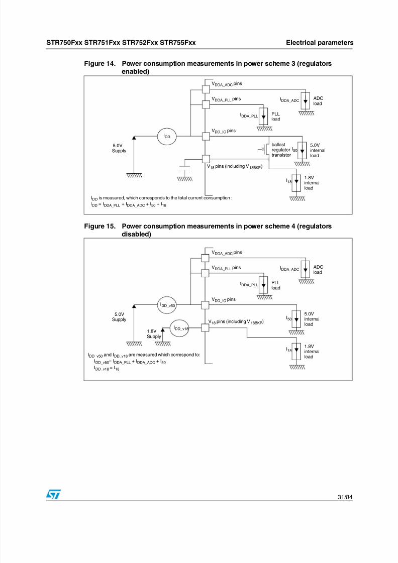
Figure 14. Power consumption measurements in power scheme 3 (regulatorsenabled)
Figure 15. Power consumption measurements in power scheme 4 (regulatorsdisabled)
VDD_IO pins
V18 pins (including V18BKP)
IDD
5.0VSupply
ballastregulatortransistor
5.0Vinternalload
1.8Vinternalload
IDD is measured, which corresponds to the total current consumption :
I50
I18
IDD = IDDA_PLL + IDDA_ADC + I50 + I18
VDDA_PLL pins
PLLload
IDDA_PLL
ADCload
IDDA_ADC
VDDA_ADC pins
VDD_IO pins
V18 pins (including V18BKP)
IDD_v50
5.0VSupply
5.0Vinternalload
1.8Vinternalload
I50
I18
VDDA_PLL pins
PLLload
IDDA_PLL
ADCload
IDDA_ADC
VDDA_ADC pins
IDD_v181.8VSupply
IDD_v50 and IDD_v18 are measured which correspond to:
IDD_v50= IDDA_PLL + IDDA_ADC + I50
IDD_v18 = I18

8/8/2019 11260
http://slidepdf.com/reader/full/11260 32/84
Electrical parameters STR750Fxx STR751Fxx STR752Fxx STR755Fxx
32/ 84
6.2 Absolute maximum ratings
Stresses above those listed as “absolute maximum ratings” may cause permanent damageto the device. This is a stress rating only and functional operation of the device under theseconditions is not implied. Exposure to maximum rating conditions for extended periods mayaffect device reliability.
6.2.1 Voltage characteristics
Table 7. Voltage characteristics
Symbol Ratings Min Max Unit
VDD_x - VSS_X(1)
1. All 3.3 V or 5.0 V power (VDD_IO, VDDA_ADC, VDDA_PLL) and ground (VSS_IO, VSSA_ADC, VDDA_ADC) pinsmust always be connected to the external 3.3V or 5.0V supply. When powered by 3.3V, I/Os are not 5Vtolerant.
Including VDDA_ADC and VDDA_PLL -0.3 6.5 V
V18 - VSS18
Digital 1.8 V Supply voltage on all V18
power pins (when 1.8 V is provided
externally)
-0.3 2.0
VIN Input voltage on any pin (2)
2. IINJ(PIN) must never be exceeded. This is implicitly insured if VIN maximum is respected. If VIN maximumcannot be respected, the injection current must be limited externally to the IINJ(PIN) value. A positiveinjection is induced by VIN>VDD while a negative injection is induced by VIN<VSS. For true open-drain pads,there is no positive injection current, and the corresponding V IN maximum must always be respected
VSS-0.3 toVDD_IO+0.3
VSS-0.3 toVDD_IO+0.3
|ΔVDDx|Variations between different 3.3 V or
5.0 V power pins50
mV|ΔV18x|Variations between different 1.8 V power
pins(3)
3. Only when using external 1.8 V power supply. All the power (V18, V18REG, V18BKP) and ground (VSS18,VSSBKP) pins must always be connected to the external 1.8 V supply.
25
|VSSX - VSS|Variations between all the different
ground pins50
VESD(HBM)Electro-static discharge voltage (Human
Body Model)
see : Absolute
maximum
ratings
(electrical sensitivity) on
page 52
see : Absolute
maximum
ratings
(electrical sensitivity) on
page 52
VESD(MM)Electro-static discharge voltage (MachineModel)

8/8/2019 11260
http://slidepdf.com/reader/full/11260 33/84
STR750Fxx STR751Fxx STR752Fxx STR755Fxx Electrical parameters
33/ 84
6.2.2 Current characteristics
6.2.3 Thermal characteristics
Table 8. Current characteristics
Symbol Ratings
Maximum
value Unit
IVDD_IO(1)
1. The user can use GPIOs to source or sink high current (up to 20 mA for O8 type High Sink I/Os). In thiscase, the user must ensure that these absolute max. values are not exceeded (taking into account theRUN power consumption) and must follow the rules described in Section 6.3.8: I/O port pin characteristics on page 54 .
Total current into VDD_IO power lines (source) (2)
2. All 3.3 V or 5.0 V power (VDD_IO, VDDA_ADC, VDDA_PLL) and ground (VSS_IO, VSSA_ADC, VDDA_ADC) pinsmust always be connected to the external 3.3V or 5.0V supply.
150
mA
IVSS_IO(1) Total current out of VSS ground lines (sink) (2) 150
IIOOutput current sunk by any I/O and control pin 25
Output current source by any I/Os and control pin - 25
IINJ(PIN)(3) & (4)
3. IINJ(PIN) must never be exceeded. This is implicitly insured if VIN maximum is respected. If VIN maximumcannot be respected, the injection current must be limited externally to the IINJ(PIN) value. A positiveinjection is induced by VIN>VDD while a negative injection is induced by V IN<VSS. Data based on TA=25°C.
4. Negative injection disturbs the analog performance of the device. See note in Section 6.3.12: 10-bit ADC characteristics on page 72 .
Injected current on NRSTIN pin ± 5
Injected current on XT1 and XT2 pins ± 5
Injected current on any other pin (5)
5. When several inputs are submitted to a current injection, the maximum ΣIINJ(PIN) is the absolute sum of thepositive and negative injected currents (instantaneous values). These results are based oncharacterization with ΣIINJ(PIN) maximum current injection on four I/O port pins of the device.
± 5
ΣIINJ(PIN)(3) Total injected current (sum of all I/O and control pins) (5) ± 25
Table 9. Thermal characteristics
Symbol Ratings Value Unit
TSTG Storage temperature range -65 to +150 °C
TJ Maximum junction temperature 150 °C

8/8/2019 11260
http://slidepdf.com/reader/full/11260 34/84
Electrical parameters STR750Fxx STR751Fxx STR752Fxx STR755Fxx
34/ 84
6.3 Operating conditions
6.3.1 General operating conditions
Subject to general operating conditions for VDD_IO, and TA unless otherwise specified.
Table 10. General operating conditions
Symbol Parameter Conditions Min Max Unit
fHCLK Internal AHB Clock frequency
Accessing SRAM with 0 wait
states0 64
MHz
Accessing Flash in burst
mode, TA≤85° C0 60
Accessing Flash in burst
mode
TA>85° C
56
Accessing Flash with 0 wait
states0 32
Write access to Flash
registers(1)
1. Write access to Flash registers is either a program, erase, set protection or un-set protection operation.
0 30
Accessing Flash in RWW
mode0 16
fPCLK Internal APB Clock frequency 0 32 MHz
VDD_IO
Standard Operating Voltage
Power Scheme 1 & 23.0 3.6
VStandard Operating Voltage
Power Scheme 3 & 44.5 5.5
V18Standard Operating Voltage
Power Scheme 2 & 41.65 1.95
PD
Power dissipation at TA= 85° C
for suffix 6 or TA= 105° C for
suffix 7(2)
2. If TA is lower, higher PD values are allowed as long as T J does not exceed TJmax (see Section 7.2: Thermal characteristics on page 79 ).
LQFP100 434
mWLQFP64 444
LFBGA100 487
LFBGA64 344
TA
Ambient temperature for 6 suffix
version
Maximum power dissipation -40 85 °C
Low power dissipation(3)
3. In low power dissipation state, TA can be extended to this range as long as TJ does not exceed TJmax (seeSection 7.2: Thermal characteristics on page 79 ).
-40 105 °C
Ambient temperature for 7 suffixversion
Maximum power dissipation -40 105 °CLow power dissipation (3) -40 125 °C
TJ Junction temperature range6 Suffix Version -40 105 °C
7 Suffix Version -40 125 °C

8/8/2019 11260
http://slidepdf.com/reader/full/11260 35/84
STR750Fxx STR751Fxx STR752Fxx STR755Fxx Electrical parameters
35/ 84
6.3.2 Operating conditions at power-up / power-down
Subject to general operating conditions for TA.
6.3.3 Embedded voltage regulators
Subject to general operating conditions for VDD_IO
, and TA
Table 11. Operating conditions at power-up / power-down
Symbol Parameter Conditions Min(1)
1. Data guaranteed by characterization, not tested in production.
Typ Max(1) Unit
tVDD_IO VDD_IO rise time rate20 μs/V
20 ms/V
tV18 V18 rise time rate (1) When 1.8 V power is supplied
externally
20 μs/V
20 ms/V
Table 12. Embedded voltage regulators
Symbol Parameter Conditions Min Typ Max Unit
VMVREG MVREG power supply(1)
1. VMVREG is observed on the V18, V18REG and V18BKP pins except in the following case:- In STOP mode with MVREG OFF (LP_PARAM13 bit). See note 2.- In STANDBY mode. See note 2.
load <150 mA 1.65 1.80 1.95 V
VLPVREG LPVREG power supply(2)
2. In STANDBY mode, VLPVREG is observed on the V18BKP pinIn STOP mode, VLPVREG is observed on the V18, V18REG and V18BKP pins.
load <10 mA 1.30 1.40 1.50 V
tVREG_PWRUP(1)
Voltage Regulators star t-up
time (to reach 90% of final V18
value) at VDD_IO power-up(3)
3. Once VDD_IO has reached 3.0 V, the RSM (Regulator Startup Monitor) generates an internal RESETduring this start-up time.
VDD_IO rise
slope = 20 µs/V80 µs
VDD_IO rise
slope = 20 ms/V35 ms

8/8/2019 11260
http://slidepdf.com/reader/full/11260 36/84
Electrical parameters STR750Fxx STR751Fxx STR752Fxx STR755Fxx
36/ 84
6.3.4 Supply current characteristics
The current consumption is measured as described in Figure 12 on page 30 and Figure 13 on page 30 .
Subject to general operating conditions for VDD_IO, and TA
Maximum power consumption
For the measurements in Table 13 and Table 14 , the MCU is placed under the followingconditions:
● All I/O pins are configured in output push-pull 0
● All peripherals are disabled except if explicitly mentioned.
● Embedded Regulators are used to provide 1.8 V (except if explicitly mentioned).
Table 13. Maximum power consumption in RUN and WFI modes
Symbol Parameter Conditions (1)
1. The conditions for these consumption measurements are described at the beginning of Section 6.3.4 .
Typ(2)
2. Typical data are based on TA=25°C, VDD_IO=3.3V or 5.0V and V18=1.8V unless otherwise specified.
Max (3)
3. Data based on product characterisation, tested in production at VDD_IO max and V18 max (1.95V in dualsupply mode or regulator output value in single supply mode) and TA max.
Unit
IDD
Supply current in
RUN mode
External Clock with PLL
multiplication, code running from
RAM, all peripherals enabled in the
MRCC_PLCKEN register: fHCLK=60
MHz, fPCLK=30 MHz
Single supply scheme see Figure 12
/ Figure 14
3.3V
and 5V
range
80 90 mA
Supply current in
WFI mode
External Clock, code running from
RAM: fHCLK=60 MHz, fPCLK=30 MHz
Single supply scheme see
Figure 12 ./ Figure 14
Parameter setting BURST=1,
WFI_FLASHEN=1
3.3V
and 5V
range
62 67 mA

8/8/2019 11260
http://slidepdf.com/reader/full/11260 37/84
STR750Fxx STR751Fxx STR752Fxx STR755Fxx Electrical parameters
37/ 84
Table 14. Maximum power consumption in STOP and STANDBY modes
Symbol Parameter Conditions (1) Typ(2)
Max(3)
UnitTA
25°C
TA
85°C
TA
105°C
IDD
Supply
current in
STOP mode
LP_PARAM bits: ALL OFF(4)
Single supply scheme see Figure 12 .
3.3V
range12 16 117 250 μA
LP_PARAM bits: ALL OFF
Dual supply scheme see Figure 13 .
IDD_V18
IDD_V33
5
<1
8
3
60
20
110
26μA
LP_PARAM bits: ALL OFF(4)
Single supply scheme see Figure 10
5V
range15 22 160 310 μA
LP_PARAM bits: ALL OFF
Dual supply scheme see Figure 11
IDD_V18
IDD_V50
5
3
8
6
60
50
110
65
μASupply
current inSTANDBY
mode
RTC OFF
3.3 V
range
10 20 25 28
5V
range15 25 30 33
1. The conditions for these consumption measurements are described at the beginning of Section 6.3.4 .
2. Typical data are based on TA=25°C, VDD_IO=3.3V or 5.0V and V18=1.8V unless otherwise specified.
3. Data based on product characterisation, tested in production at VDD_IO max and V18 max (1.95V in dual supply mode orregulator output value in single supply mode).
4. In this mode, the whole digital circuitry is powered internally by the LPVREG at approximately 1.4V, which significantlyreduces the leakage currents.

8/8/2019 11260
http://slidepdf.com/reader/full/11260 38/84
Electrical parameters STR750Fxx STR751Fxx STR752Fxx STR755Fxx
38/ 84
Figure 16. Power consumption in STOP modein Single supply scheme (3.3 Vrange)
Figure 17. Power consumption in STOP modeSingle supply scheme (5 V range)
0
50
100
150
200
250
300
-40 25 45 55 75 95 105
Temp (°C)
I S t o p
( u A )
TYP (3.3V)
MAX (3.6V)
0
50
100
150
200
250
300
350
-40 25 45 55 75 95 105
Temp (°C)
I S t o p
( u A )
TYP (5.0V)
MAX (5.5V)
Figure 18. Power consumption in STANDBYmode (3.3 V range)
Figure 19. Power consumption in STANDBYmode (5 V range)
0
5
10
15
20
25
30
-40 25 105
Temp (°C)
I S t a n d b y
( u A )
TYP (3.3V)
MAX (3.6V)
0
5
10
15
20
25
30
35
-40 25 105
Temp (°C)
I S t
a n d b y
( u A )
TYP (5.0V)
MAX (5.5V)

8/8/2019 11260
http://slidepdf.com/reader/full/11260 39/84
STR750Fxx STR751Fxx STR752Fxx STR755Fxx Electrical parameters
39/ 84
Typical power consumption
The following measurement conditions apply to Table 15 , Table 16 and Table 17 .
In RUN mode:
● Program is executed from Flash (except if especially mentioned). The program consistsof an infinite loop. When fHCLK > 32 MHz, burst mode is activated.
● A standard 4 MHz crystal source is used.
● In all cases the PLL is used to multiply the frequency.
● All measurements are done in the single supply scheme with internal regulators used(see Figure 12 )
In WFI Mode:
● In WFI Mode the measurement conditions are similar to RUN mode (OSC4M and PLLenabled). In addition, the Flash can be disabled depending on burst mode activation:
– For AHB frequencies greater than 32 MHz, burst mode is activated and the Flashis kept enabled by setting the WFI_FLASH_EN bit (this bit cannot be reset whenburst mode is activated).
– For AHB frequencies less than or equal to 32 MHz, burst mode is deactivated,WFI_FLASH_EN is reset and the LP_PARAM14 bit is set (Flash is disabled in WFImode).
In SLOW mode:
● The same program as in RUN mode is executed from Flash. The CPU is clocked by theFREEOSC, OSC4M, LPOSC or OSC32K. Only EXTIT peripheral is enabled in theMRCC_PCLKEN register.
In SLOW-WFI mode:
● In SLOW-WFI, the measurement conditions are similar to SLOW mode (CPU clocked
by a low frequency clock). In addition, the LP_PARAM14 bit is set (FLASH is OFF). TheWFI routine itself is executed from SRAM (it is not allowed to execute a WFI from theinternal FLASH)
In STOP mode:
● Several measurements are given: in the single supply scheme with internal regulatorsused (see Figure 12 ): and in the dual supply scheme (see Figure 13 ).
In STANDBY mode:
● Three measurements are given:
– The RTC is disabled, only the consumption of the LPVREG and RSM remain(almost no leakage currents)
– The RTC is running, clocked by a standard 32.768 kHz crystal.
– The RTC is running, clocked by the internal Low Power RC oscillator (LPOSC)
● STANDBY mode is only supported in the single supply scheme (see Figure 12 )

8/8/2019 11260
http://slidepdf.com/reader/full/11260 40/84
Electrical parameters STR750Fxx STR751Fxx STR752Fxx STR755Fxx
40/ 84
Subject to general operating conditions for VDD_IO, and TA
Table 15. Single supply typical power consumption in Run, WFI, Slow and Slow-WFI modes
Symbol Para meter Conditions3.3V
typ(1)
5V
typ(2)Unit
IDD(3)
Supply current in
RUN mode(4)
Clocked by OSC4M with PLL multiplication, all peripherals
enabled in the MRCC_PLCKEN register:
fHCLK=60 MHz, fPCLK=30 MHz
fHCLK=56 MHz, fPCLK=28 MHz
fHCLK=48 MHz, fPCLK=24 MHz
fHCLK=32 MHz, fPCLK=32 MHz
fHCLK=16 MHz, fPCLK=16 MHz
fHCLK=8 MHz, fPCLK=8 MHz
80
75
65
59
34
20
82
77
67
61
37
22
mA
Clocked by OSC4M with PLL multiplication, only EXTIT
peripheral enabled in the MRCC_PLCKEN register:
fHCLK=60 MHz, fPCLK=30 MHz
fHCLK=56 MHz, fPCLK=28 MHzfHCLK=48 MHz, fPCLK=24 MHz
fHCLK=32 MHz, fPCLK=32 MHz
fHCLK=16 MHz, fPCLK=16 MHz
fHCLK=8 MHz, fPCLK=8 MHz
65
6054
42
22
16
67
6255
44
24
18
mA
Supply current in
WFI mode(4)
Clocked by OSC4M with PLL multiplication, only EXTIT
peripheral enabled in the MRCC_PLCKEN register:
fHCLK=60 MHz, fPCLK=30 MHz(5)
fHCLK=56 MHz, fPCLK=28 MHz(5)
fHCLK=48 MHz, fPCLK=24 MHz(5)
fHCLK=32 MHz, fPCLK=32 MHz(6)
fHCLK=16 MHz, fPCLK= 16 MHz (6)
fHCLK= 8 MHz, fPCLK= 8 MHz(6)
62
59
53
22
13
10
63
60
54
23
15
11
mA
Supply current in
SLOW mode(4)
Clocked by FREEOSC: fHCLK=fPCLK=~5 MHz,
Clocked by OSC4M: fHCLK=fPCLK=4 MHz
Clocked by LPOSC: fHCLK=fPCLK=~300 kHz
Clocked by OSC32K: fHCLK=fPCLK=32.768 kHz
9
8
3.65
3.5
10
9
3.9
4.2
mA
Supply current in
SLOW-WFI
mode(4)(7)
Clocked by FREEOSC: fHCLK=fPCLK=~5 MHz
Clocked by OSC4M: fHCLK=fPCLK=4 MHz
Clocked by LPOSC: fHCLK=fPCLK=~300 kHz
Clocked by OSC32K: fHCLK=fPCLK=32.768 kHz
3.5
3.1
1.15
0.98
4.0
3.75
1.65
1.5
mA
1. Typical data based on TA=25° C and VDD_IO=3.3V.
2. Typical data based on TA=25° C and VDD_IO=5.0V.
3. The conditions for these consumption measurements are described at the beginning of Section 6.3.4 on page 36 .
4. Single supply scheme see Figure 14 .5. Parameter setting BURST=1, WFI_FLASHEN=1
6. Parameter setting BURST=0, WFI_FLASHEN=0
7. Parameter setting WFI_FLASHEN=0, OSC4MOFF=1

8/8/2019 11260
http://slidepdf.com/reader/full/11260 41/84
STR750Fxx STR751Fxx STR752Fxx STR755Fxx Electrical parameters
41/ 84
Subject to general operating conditions for VDD_IO, and TA
Table 16. Dual supply supply typical power consumption in Run, WFI, Slow andSlow-WFI modes
To calculate the power consumption in Dual supply mode, refer to the values given in Table 15 . and
consider that this consumption is split as follows:
IDD(single supply)~IDD(dual supply)= IDD_V18 + IDD(VDD_IO)
For 3.3V range: IDD(VDD_IO) ~ 1 to 2 mA
For 5V range: IDD(VDD_IO) ~ 2 to 3 mA
Therefore most of the consumption is sunk on the V18 power supply
This formula does not apply in STOP and STANDBY modes, refer to Table 17 .
Table 17. Typical power consumption in STOP and STANDBY modes
Symbol Parameter Conditions 3.3VTyp(1) 5V
Typ(2) Unit
IDD(3)
Supply current
in STOP
mode(4)
LP_PARAM bits: ALL OFF(5) 12 15
μA
LP_PARAM bits : MVREG ON, OSC4M OFF, FLASH
OFF(6) 130 135
LP_PARAM bits: MVREG ON, OSC4M ON , FLASH
OFF(6) 1950 1930
LP_PARAM bits: MVREG ON, OSC4M OFF, FLASH ON (6) 630 635
LP_PARAM bits: MVREG ON, OSC4M ON, FLASH ON (6) 2435 2425
Supply current
in STOP
mode(7)
LPPARAM bits: ALL OFF, with V18=1.8 VIDD_V18
IDD_V33
5
<1
5
<1
μA
LP_PARAM bits: OSC4M ON, FLASH OFFIDD_V18IDD_V33
410
1475
410
1435
LP_PARAM bits: OSC4M OFF, FLASH ONIDD_V18IDD_V33
550
<1
550
1
LP_PARAM bits: OSC4M ON, FLASH ONIDD_V18IDD_V33
910
1475
910
1445
Supply current
in STANDBY
mode(4)
RTC OFF 11 14
μARTC ON clocked by OSC32K 14 18
1. Typical data are based on TA=25°C, VDD_IO=3.3 V and V18=1.8 V unless otherwise indicated in the table.
2. Typical data are based on TA=25°C, VDD_IO=5.0 V and V18=1.8 V unless otherwise indicated in the table.
3. The conditions for these consumption measurements are described at the beginning of Section 6.3.4 on page 36 .
4. Single supply scheme see Figure 12 .
5. In this mode, the whole digital circuitry is powered internally by the LPVREG at approximately 1.4 V, which significantlyreduces the leakage currents.
6. In this mode, the whole digital circuitry is powered internally by the MVREG at 1.8 V.
7. Dual supply scheme see Figure 13 .

8/8/2019 11260
http://slidepdf.com/reader/full/11260 42/84
Electrical parameters STR750Fxx STR751Fxx STR752Fxx STR755Fxx
42/ 84
Supply and clock manager power consumption
Table 18. Supply and clock manager power consumption
Symbol Parameter Conditions
(1) 3.3V
Typ
5V
Typ Unit
IDD(OSC4M)
Supply current of resonator oscillator
in STOP or WFI mode (LP_PARAM
bit: OSC4M ON)
External components specified in:
4/8 MHz crystal / ceramic resonator
oscillator (XT1/XT2) on page 46
1815 1795
μA
IDD(FLASH)
FLASH static current consumption in
STOP or WFI mode (LP_PARAM bit
FLASH ON)
515 515
IDD(MVREG)
Main Voltage Regulator static current
consumption in STOP mode
(LP_PARAM bit: MVREG ON)
130 135
IDD(LPVREG)Low Power Voltage Regulator + RSM
current static current consumption
STOP mode includes leakage
where V18 is internally set to 1.4 V12 15
STANDBY mode where
V18BKP and V18 are internally set to
1.4 V and 0 V respectively
11 14
1. Measurements performed in 3.3V single supply mode see Figure 12

8/8/2019 11260
http://slidepdf.com/reader/full/11260 43/84
STR750Fxx STR751Fxx STR752Fxx STR755Fxx Electrical parameters
43/ 84
On-Chip peripheral power consumption
Conditions:
– VDD_IO=VDDA_ADC=VDDA_PLL=3.3 V or 5 V ±10% unless otherwise specified.
– TA= 25° C– Clocked by OSC4M with PLL multiplication, fCK_SYS=64 MHz, fHCLK=32 MHz,
fPCLK=32 MHz
.
Table 19. On-Chip peripherals
Symbol ParameterTyp
(3.3V and 5.0V)Unit
IDD(TIM) TIM Timer supply current (1)
1. Data based on a differential IDD measurement between reset configuration and timer counter running at 32MHz. No IC/OC programmed (no I/O pads toggling)
0.7
mA
IDD(PWM) PWM Timer supply current(2)
2. Data based on a differential IDD measurement between reset configuration and PWM running at 32 MHz.This measurement does not include PWM pads toggling consumption.
1
IDD(SSP) SSP supply current (3)
3. Data based on a differential IDD measurement between reset configuration and permanent SPI mastercommunication at maximum speed 16 MHz. The data sent is 55h. This measurement does not include thepad toggling consumption.
1.3
IDD(UART) UART supply current (4)
4. Data based on a differential IDD measurement between reset configuration and a permanent UART datatransmit sequence at 1Mbauds. This measurement does not include the pad toggling consumption.
1.6
IDD(I2C) I2C supply current (5)
5. Data based on a differential IDD measurement between reset configuration (I2C disabled) and a permanentI2C master communication at 100kHz (data sent equal to 55h). This measurement includes the padtoggling consumption but not the external 10kOhm external pull-up on clock and data lines.
0.3
IDD(ADC) ADC supply current when converting (6)
6. Data based on a differential IDD measurement between reset configuration and continuous A/Dconversions at 8 MHz in scan mode on 16 inputs configured as AIN.
1.2
IDD(USB)
USB supply current (7)
Note: VDD_IO must be 3.3 V ±10%
7. Data based on a differential IDD measurement between reset configuration and a running generic HIDapplication.
0.90
IDD(CAN) CAN supply current (8)
8. Data based on a differential IDD measurement between reset configuration (CAN disabled) and apermanent CAN data transmit sequence in loopback mode at 1MHz. This measurement does not includethe pad toggling consumption.
2.8

8/8/2019 11260
http://slidepdf.com/reader/full/11260 44/84
Electrical parameters STR750Fxx STR751Fxx STR752Fxx STR755Fxx
44/ 84
6.3.5 Clock and timing characteristics
XT1 external clock source
Subject to general operating conditions for VDD_IO, and TA.
Table 20. XT1 external clock source
Symbol Parameter Conditions(1) (2)
1. Data based on typical application software.
2. Time measured between interrupt event and interrupt vector fetch. Δtc(INST) is the number of tCPU cyclesneeded to finish the current instruction execution.
Min Typ Max Unit
fXT1External clock source
frequency
see Figure 20
4 60 MHz
VXT1HXT1 input pin high level
voltage0.7xVDD_IO VDD_IO
V
VXT1LXT1 input pin low level
voltageVSS 0.3xVDD_IO
tw(XT1H)
tw(XT1L)
XT1 high or low time (3)
3. Data based on design simulation and/or technology characteristics, not tested in production.
6
nstr(XT1)
tf(XT1)XT1 rise or fall time (3) 20
IL XTx Input leakage currentVSS ≤ VIN ≤
VDD_IO±1 μA
CIN(XT1) XT1 input capacitance(3) 5 pF
DuCy(XT1) Duty cycle 45 55 %

8/8/2019 11260
http://slidepdf.com/reader/full/11260 45/84
STR750Fxx STR751Fxx STR752Fxx STR755Fxx Electrical parameters
45/ 84
XRTC1 external clock source
Subject to general operating conditions for VDD_IO, and TA.
Figure 20. Typical application with an external clock source
Table 21. XRTC1 external clock source
Symbol Parameter Conditions(1)
1. Data based on typical application software.
Min Typ Max Unit
fXRTC1External clock source
frequency
see Figure 20
32.768 500 kHz
VXRTC1HXRTC1 input pin high
level voltage0.7xVDD_IO VDD_IO
V
VXRTC1LXRTC1 input pin low
level voltageVSS 0.3xVDD_IO
tw(XRTC1H)tw(XRTC1L)
XRTC1 high or low
time(2)
2. Data based on design simulation and/or technology characteristics, not tested in production.
900
nstr(XRTC1)
tf(XRTC1) XRTC1 rise or fall time(2)
50
ILXRTCx Input leakage
current
VSS≤VIN≤VDD_I
O±1 μA
CIN(RTC1)XRTC1 input
capacitance(2) 5 pF
DuCy(RTC1) Duty cycle 30 70 %
XT1
XT2 fOSC4M
EXTERNAL
STR750
CLOCK SOURCE
VXT1L
VXT1H
tr(XT1) tf(XT1) tw(XT1H) tw(XT1L)
IL
90%
10%
TXT1
hi-Z

8/8/2019 11260
http://slidepdf.com/reader/full/11260 46/84
Electrical parameters STR750Fxx STR751Fxx STR752Fxx STR755Fxx
46/ 84
4/8 MHz crystal / ceramic resonator oscillator (XT1/XT2)
The STR750 system clock or the input of the PLL can be supplied by a OSC4M which is a 4MHz clock generated from a 4 MHz or 8 MHz crystal or ceramic resonator. If using an 8 MHzoscillator, software set the XTDIV bit to enable a divider by 2 and generate a 4 MHz OSC4M
clock. All the information given in this paragraph are based on product characterisation withspecified typical external components. In the application, the resonator and the loadcapacitors have to be placed as close as possible to the oscillator pins in order to minimizeoutput distortion and start-up stabilization time. Refer to the crystal/ceramic resonatormanufacturer for more details (frequency, package, accuracy...).
Figure 21. Typical application with a 4 or 8 MHz crystal or ceramic resonator
Table 22. 4/8 MHz crystal / ceramic resonator oscillator (XT1/XT2)(1)
Symbol Parameter Conditions Min Typ Max Unit
fOSC4M Oscillator frequency
4 MHz Crystal/Resonator Oscillator
connected on XT1/XT2 XTDIV=0
or
8 MHz Crystal/Resonator Oscillatorconnected on XT1/XT2 XTDIV=1
4 MHz
RF Feedback resistor 200 240 270 kΩ
CL1(2)
CL2
Recommended load
capacitance versus equivalent
serial resistance of the crystal or
ceramic resonator (RS)(3)
RS=200Ω 60 pF
i2 XT2 driving current VDD_IO=3.3 V or 5.0 V 425 μA
tSU(OSC4M)(4) Startup time at VDD_IO power-up 1 ms
1. Resonator characteristics given by the crystal/ceramic resonator manufacturer.
2. For CL1
and CL2
it is recommended to use high-quality ceramic capacitors in the 5-pF to 25-pF range (typ.) designed forhigh-frequency applications and selected to match the requirements of the crystal or resonator. CL1 and CL2, are usually thesame size. The crystal manufacturer typically specifies a load capacitance which is the series combination of C L1 and CL2.PCB and MCU pin capacitance must be included when sizing CL1 and CL2 (10 pF can be used as a rough estimate of thecombined pin and board capacitance).
3. The relatively low value of the RF resistor offers a good protection against issues resulting from use in a humidenvironment, due to the induced leakage and the bias condition change. However, it is recommended to take this point intoaccount if the MCU is used in tough humidity conditions.
4. tSU(OSC4M) is the typical start-up time measured from the moment VDD_IO is powered (with a quick VDD_IO ramp-up from 0to 3.3V (<50μs) to a stabilized 4MHz oscillation is reached. This value is measured for a standard crystal resonator and itcan vary significantly with the crystal/ceramic resonator manufacturer.
XT2
XT1
fOSC4M
CL1
CL2
i2
RF
STR75X
RESONATOR
WHEN RESONATOR WITH
INTEGRATED CAPACITORS
VDD /2Ref
FEEDBACKLOOP
LINEAR
AMPLIFIER
XTDIV
/2

8/8/2019 11260
http://slidepdf.com/reader/full/11260 47/84
STR750Fxx STR751Fxx STR752Fxx STR755Fxx Electrical parameters
47/ 84
OSC32K crystal / ceramic resonator oscillator
The STR7 RTC clock can be supplied with a 32.768 kHz Crystal/Ceramic resonatoroscillator. All the information given in this paragraph are based on product characterisationwith specified typical external components. In the application, the resonator and the load
capacitors have to be placed as close as possible to the oscillator pins in order to minimizeoutput distortion and start-up stabilization time. Refer to the crystal/ceramic resonatormanufacturer for more details (frequency, package, accuracy...).
Figure 22. Typical application with a 32.768 kHz crystal or ceramic resonator
PLL characteristics
PLL Jitter Terminology
●
Self-referred single period jitter (period jitter)Period Jitter is defined as the difference of the maximum period (Tmax) and minimumperiod (Tmin) at the output of the PLL where Tmax is the maximum time differencebetween 2 consecutive clock rising edges and Tmin is the minimum time differencebetween 2 consecutive clock rising edges.
See Figure 23
● Self-referred long term jitter (N period jitter)
Self-referred long term Jitter is defined as the difference of the maximum period (Tmax)and minimum period (Tmin) at the output of the PLL where Tmax is the maximum time
Table 23. OSC32K crystal / ceramic resonator oscillator
Symbol Parameter Conditions Min Typ Max Unit
fOSC32K Oscillator Frequency 32.768 kHz
RF Feedback resistor VDD_IO=3.3 V or 5.0 V 270 310 370 kΩ
CL1
CL2
Recommended load capacitance
versus equivalent serial resistance of
the crystal or ceramic resonator (RS)
(1)RS=40KΩ 12.5 15 pF
i2 XT2 driving currentVDD_IO=3.3 V or 5.0 V
VIN=VSS1 5 μA
tSU(OSC32K)(2) Startup time VDD_IO is stabilized 2.5 s
1. The oscillator selection can be optimized in terms of supply current using an high quality resonator with small RS value.Refer to crystal/ceramic resonator manufacturer for more details
2. tSU(OSC32K) is the start-up time measured from the moment it is enabled (by software) to a stabilized 32 kHz oscillation isreached. This value is measured for a standard crystal resonator and it can vary significantly with the crystal/ceramicresonator manufacturer
XRTC2
XRTC1 fOSC32KCL1
CL2
i2
RF
STR750
32 kHz
WHEN RESONATOR WITH
INTEGRATED CAPACITORS
RESONATOR
FEEDBACK
LOOP

8/8/2019 11260
http://slidepdf.com/reader/full/11260 48/84
Electrical parameters STR750Fxx STR751Fxx STR752Fxx STR755Fxx
48/ 84
difference between N+1 consecutive clock rising edges and Tmin is the minimum timedifference between N+1 consecutive clock rising edges.
N should be kept sufficiently large to have a long term jitter (ex: thousands).
For N=1, this becomes the single period jitter.
See Figure 23
● Cycle-to-cycle jitter (N period jitter)
This corresponds to the time variation between adjacent cycles over a random sampleof adjacent clock cycles pairs. Jitter(cycle-to-cycle) = Max(Tcycle n- Tcycle n-1) for n=1to N.
See Figure 24
Figure 23. Self-referred jitter (single and long term)
Figure 24. Cycle-to-cycle jitter
IDEALCK_PLL
trigger point
ACTUALCK_PLL
n n+1 n+N---
long term jitter
T
single period jitter
IDEALCK_PLL
ACTUALCK_PLL
n n+1
T
Tcycle 1 Tcycle 2
n+2 ---
Tcycle N-1
n+N

8/8/2019 11260
http://slidepdf.com/reader/full/11260 49/84
STR750Fxx STR751Fxx STR752Fxx STR755Fxx Electrical parameters
49/ 84
PLL characteristics
Subject to general operating conditions for VDD_IO, and TA.
Internal RC oscillators (FREEOSC & LPOSC)
Subject to general operating conditions for VDD_IO, and TA.
Table 24. PLL characteristics
Symbol Parameter Test ConditionsValue
UnitMin Typ Max(1)
1. Data based on product characterisation, not tested in production.
fPLL_IN
PLL input clock 4.0 MHz
PLL input clock duty cycle 40 60 %
fPLL_OUT PLL multiplier output clock fPLL_INx 24 165 MHz
fVCO VCO frequency rangeWhen PLL
operates (locked)336 960 MHz
tLOCK PLL lock time 300 μs
ΔtJITTER1(2)(3)
2. Refer to jitter terminology in : PLL characteristics on page 47 for details on how jitter is specified.
3. The jitter specification holds true only up to 50mV (peak-to-peak) noise on VDDA_PLL and V18 supplies.Jitter will increase if the noise is more than 50mV. In addition, it assumes that the input clock has no jitter.
Single period jitter (+/-3Σ peakto peak) fPLL_IN = 4 MHz
(4)
VDD_IO is stable
4. The PLL parameters (MX1, MX0, PRESC1, PRESC2) must respect the constraints described in: PLLcharacteristics on page 47 .
+/-250 ps
ΔtJITTER2(2)(3) Long term jitter (+/-3Σ peak to
peak)
fPLL_IN = 4 MHz(4)
VDD_IO is stable+/-2.5 ns
ΔtJITTER3(2)(3) Cycle to cycle jitter (+/-3Σ peak
to peak)
fPLL_IN = 4 MHz(4)
VDD_IO is stable+/-500 ps
Table 25. Internal RC oscillators (FREEOSC & LPOSC)
Symbol Parameter Conditions Min Typ Max Unit
fCK_FREEOSC FREEOSC Oscillator Frequency 3 5 8 MHz
fCK_LPOSC LPOSC Oscillator Frequency 150 300 500 kHz

8/8/2019 11260
http://slidepdf.com/reader/full/11260 50/84
Electrical parameters STR750Fxx STR751Fxx STR752Fxx STR755Fxx
50/ 84
6.3.6 Memory characteristics
Flash memory
Subject to general operating conditions for VDD_IO and V18, TA = -40 to 105 °C unless
otherwise specified.
Table 26. Flash memory characteristics
Symbol Parameter Test ConditionsValue
UnitTyp Max(1)
1. Data based on characterisation not tested in production
tPW Word Program 35 μs
tPDW Double Word Program 60 μs
tPB0 Bank 0 Program (256K)Single Word programming of
a checker-board pattern2 4.9(2)
2. 10K program/erase cycles.
s
tPB1 Bank 1 Program (16K) Single Word programming ofa checker-board pattern
125 224(2) ms
tES Sector Erase (64K)Not preprogrammed (all 1)
Preprogrammed (all 0)
1.54
1.176
2.94(2)
2.38(2) s
tES Sector Erase (8K)Not preprogrammed (all 1)
Preprogrammed (all 0)
392
343
560(2)
532(2) ms
tES Bank 0 Erase (256K)Not preprogrammed (all 1)
Preprogrammed (all 0)
8.0
6.6
13.7
11.2s
tES Bank 1 Erase (16K)Not preprogrammed (all 1)
Preprogrammed (all 0)
0.9
0.8
1.5
1.3s
tRPD Recovery when disabled 20 μs
tPSL Program Suspend Latency 10 μs
tESL Erase Suspend Latency 300 μs
Table 27. Flash memory endurance and data retention
Symbol Parameter ConditionsValue
UnitMin(1)
1. Data based on characterisation not tested in production.
Typ Max
NEND_B0 Endurance (Bank 0 sectors) 10 kcycles
NEND_B1 Endurance (Bank 1 sectors) 100 kcycles
YRET Data Retention TA=85° C 20 Years
tESR Erase Suspend Rate
Min time from Erase
Resume to next Erase
Suspend20 ms

8/8/2019 11260
http://slidepdf.com/reader/full/11260 51/84
STR750Fxx STR751Fxx STR752Fxx STR755Fxx Electrical parameters
51/ 84
6.3.7 EMC characteristics
Susceptibility tests are performed on a sample basis during product characterization.
Functional EMS (electro magnetic susceptibility)
Based on a simple running application on the product (toggling 2 LEDs through I/O ports),the product is stressed by two electro magnetic events until a failure occurs (indicated by theLEDs).
● ESD: Electro-Static Discharge (positive and negative) is applied on all pins of thedevice until a functional disturbance occurs. This test conforms with the IEC 1000-4-2standard.
● FTB: A Burst of Fast Transient voltage (positive and negative) is applied to VDD andVSS through a 100pF capacitor, until a functional disturbance occurs. This testconforms with the IEC 1000-4-4 standard.
A device reset allows normal operations to be resumed. The test results are given in thetable below based on the EMS levels and classes defined in application note AN1709.
Designing hardened software to avoid noise problems
EMC characterization and optimization are performed at component level with a typicalapplication environment and simplified MCU software. It should be noted that good EMCperformance is highly dependent on the user application and the software in particular.
Therefore it is recommended that the user applies EMC software optimization andprequalification tests in relation with the EMC level requested for his application.
Software recommendations:
The software flowchart must include the management of runaway conditions such as:
● Corrupted program counter
● Unexpected reset
● Critical Data corruption (control registers...)
Prequalification trials:
Most of the common failures (unexpected reset and program counter corruption) can bereproduced by manually forcing a low state on the RESET pin or the Oscillator pins for 1second.
To complete these tr ials, ESD stress can be applied directly on the device, over the range ofspecification values. When unexpected behaviour is detected, the software can behardened to prevent unrecoverable errors occurring (see application note AN1015).
Table 28. EMC characteristics
Symbol Parameter ConditionsLevel/
Class
VFESDVoltage limits to be applied on any I/O pin to
induce a functional disturbance
VDD_IO=3.3 V or 5 V,
TA=+25° C, fCK_SYS=32 MHz
conforms to IEC 1000-4-2
Class A
VEFTB
Fast transient voltage burst limits to be applied
through 100pF on VDD and VSS pins to induce
a functional disturbance
VDD_IO=3.3 V or 5 V,
TA=+25° C, fCK_SYS=32 MHz
conforms to IEC 1000-4-4
Class A

8/8/2019 11260
http://slidepdf.com/reader/full/11260 52/84
Electrical parameters STR750Fxx STR751Fxx STR752Fxx STR755Fxx
52/ 84
Electro magnetic interference (EMI)
Based on a simple application running on the product (toggling 2 LEDs through the I/Oports), the product is monitored in terms of emission. This emission test is in line with thenorm SAE J 1752/3 which specifies the board and the loading of each pin.
Absolute maximum ratings (electrical sensitivity)
Based on three different tests (ESD, LU and DLU) using specific measurement methods, theproduct is stressed in order to determine its performance in terms of electrical sensitivity.For more details, refer to the application note AN1181.
Electro-Static discharge (ESD)
Electro-Static Discharges (a positive then a negative pulse separated by 1 second) areapplied to the pins of each sample according to each pin combination. The sample sizedepends on the number of supply pins in the device (3 parts*(n+1) supply pin). Two modelscan be simulated: Human Body Model and Machine Model. This test conforms to theJESD22-A114A/A115A standard.
Table 29. EMI characteristics
Symbo
lParameter Conditions
Monitored
Frequency Band
Max vs. [fOSC4M /fHCLK]Unit
4/32MHz 4/60MHz
SEMI Peak level
Flash devices:
VDD_IO=3.3 V or 5 V,
TA=+25° C,
LQFP64 package
conforming to SAE J
1752/3
0.1 MHz to 30 MHz 22 26
dBμV30 MHz to 130 MHz 31 26
130 MHz to 1 GHz 19 23
SAE EMI Level >4 >4 -
Table 30. Absolute maximum ratings
Symbol Ratings ConditionsMaximum
value(1)
1. Data based on product characterisation, not tested in production.
Unit
VESD(HBM)Electro-static discharge voltage
(Human Body Model)
TA=+25° C
2000
VVESD(MM)Electro-static discharge voltage
(Machine Model)200
VESD(CDM)Electro-static discharge voltage
(Charge Device Model)750

8/8/2019 11260
http://slidepdf.com/reader/full/11260 53/84
STR750Fxx STR751Fxx STR752Fxx STR755Fxx Electrical parameters
53/ 84
Static and dynamic latch-up
● LU: 3 complementary static tests are required on 10 parts to assess the latch-upperformance. A supply overvoltage (applied to each power supply pin) and a currentinjection (applied to each input, output and configurable I/O pin) are performed on each
sample. This test conforms to the EIA/JESD 78 IC latch-up standard. For more details,refer to the application note AN1181.
● DLU: Electro-Static Discharges (one positive then one negative test) are applied toeach pin of 3 samples when the micro is running to assess the latch-up performance indynamic mode. Power supplies are set to the typical values, the oscillator is connectedas near as possible to the pins of the micro and the component is put in reset mode.This test conforms to the IEC1000-4-2 and SAEJ1752/3 standards. For more details,refer to the application note AN1181.
Table 31. Electrical sensitivities
Symbol Parameter Conditions Class(1)
1. Class description: A Class is an STMicroelectronics internal specification. All its limits are higher than theJEDEC specifications, that means when a device belongs to Class A it exceeds the JEDEC standard. BClass strictly covers all the JEDEC criteria (international standard).
LU Static latch-up classTA=+25° CTA=+85° C
TA=+105° C
Class A
DLU Dynamic latch-up classVDD= 5.5 V, fOSC4M=4 MHz,
fCK_SYS=32 MHz, TA=+25° CClass A

8/8/2019 11260
http://slidepdf.com/reader/full/11260 54/84
Electrical parameters STR750Fxx STR751Fxx STR752Fxx STR755Fxx
54/ 84
6.3.8 I/O port pin characteristics
General characteristics
Subject to general operating conditions for VDD_IO and TA unless otherwise specified.
Table 32. General characteristics
I/O static characteristics
Symbol Parameter Conditions Min Typ Max Unit
VIL Input low level voltage
TTL ports
0.8V
VIH Input high level voltage 2
VhysSchmitt trigger voltage
hysteresis(1)
1. Hysteresis voltage between Schmitt trigger switching levels.
400 mV
IINJ(PIN) Injected Current on any I/O pin ± 4
mAΣIINJ(PIN(2)
2. When the current limitation is not possible, the VIN absolute maximum rating must be respected, otherwiserefer to IINJ(PIN) specification. A positive injection is induced by VIN>VDD_IO while a negative injection isinduced by VIN<VSS. Refer to Section 6.2 on page 32 for more details.
Total injected current (sum of allI/O and control pins)
± 25
Ilkg
Input leakage current on robust
pinsSee Section 6.3.12 on page 72
Input leakage current(3)
3. Leakage could be higher than max. if negative current is injected on adjacent pins.
VSS≤VIN≤VDD_IO ±1μA
IS Static current consumption(4)
4. Configuration not recommended, all unused pins must be kept at a fixed voltage: using the output mode ofthe I/O for example or an external pull-up or pull-down resistor (see Figure 25 ). Data based on designsimulation and/or technology characteristics, not tested in production.
Floating input mode 200
RPUWeak pull-up equivalent
resistor(5)
5. The RPU pull-up and RPD pull-down equivalent resistor are based on a resistive transistor.
VIN=VSS
VDD_IO=3.3 V 50 95 200 kΩ
VDD_IO=5 V 20 58 150 kΩ
RPDWeak pull-down equivalent
resistor(5) VIN=VDD_IO
VDD_IO=3.3 V 25 80 180 kΩ
VDD_IO=5 V 20 50 120 kΩCIO I/O pin capacitance 5 pF
tw(IT)inExternal interrupt/wake-up lines
pulse time(6)
6. To generate an external interrupt, a minimum pulse width has to be applied on an I/O port pin configuredas an external interrupt source.
2TAP
B

8/8/2019 11260
http://slidepdf.com/reader/full/11260 55/84
STR750Fxx STR751Fxx STR752Fxx STR755Fxx Electrical parameters
55/ 84
Figure 25. Connecting unused I/O pins
Output driving current
The GP I/Os have different drive capabilities:
● O2 outputs can sink or source up to +/-2 mA.
● O4 outputs can sink or source up to +/-4 mA.● outputs can sink or source up to +/-8 mA or can sink +20 mA (with a relaxed VOL).
In the application, the user must limit the number of I/O pins which can drive current torespect the absolute maximum rating specified in Section 6.2.2 :
● The sum of the current sourced by all the I/Os on VDD_IO, plus the maximum RUNconsumption of the MCU sourced on VDD_IO, can not exceed the absolute maximumrating IVDD_IO.
● The sum of the current sunk by all the I/Os on VSS_IO plus the maximum RUNconsumption of the MCU sunk on VSS_IO can not exceed the absolute maximum ratingIVSS_IO.
Subject to general operating conditions for VDD_IO and TA unless otherwise specified.
10kΩUNUSED I/OPORT
STR7XXX
10kΩUNUSED I/OPORT
STR7XXXVDD

8/8/2019 11260
http://slidepdf.com/reader/full/11260 56/84
Electrical parameters STR750Fxx STR751Fxx STR752Fxx STR755Fxx
56/ 84
Table 33. Output driving current
I/O Output drive characteristics for
VDD_IO = 3.0 to 3.6 V and EN33 bit =1
or VDD_IO = 4.5 to 5.5 V and EN33 bit =0
I/O
TypeSymbol Parameter Conditions Min Max Unit
O2
VOL(1)
1. The IIO current sunk must always respect the absolute maximum rating specified in Section 6.2.2 and thesum of IIO (I/O ports and control pins) must not exceed IVSS_IO.
Output low level voltage for a standard
I/O pin when 8 pins are sunk at same
time
IIO=+2 mA 0.4
V
VOH(2)
2. The IIO current sourced must always respect the absolute maximum rating specified in Section 6.2.2 andthe sum of IIO (I/O ports and control pins) must not exceed IVDD_IO.
Output high level voltage for an I/O pin
when 4 pins are sourced at same timeIIO=-2 mA VDD_IO-0.8
O4
VOL(1)
Output low level voltage for a standard
I/O pin when 8 pins are sunk at same
time
IIO=+4 mA 0.4
VOH(2) Output high level voltage for an I/O pinwhen 4 pins are sourced at same time
IIO=-4 mA VDD_IO-0.8
O8
VOL(1)
Output low level voltage for a standard
I/O pin when 8 pins are sunk at same
time
IIO=+8 mA 0.4
Output low level voltage for a high sink
I/O pin when 4 pins are sunk at same
time
IIO=+20 mA,
TA≤85°C
TA≥85°C
1.3
1.5
IIO=+8 mA 0.4
VOH(2) Output high level voltage for an I/O pin
when 4 pins are sourced at same timeIIO=-8 mA VDD_IO-0.8

8/8/2019 11260
http://slidepdf.com/reader/full/11260 57/84
STR750Fxx STR751Fxx STR752Fxx STR755Fxx Electrical parameters
57/ 84
Output speed
Subject to general operating conditions for VDD_IO and TA unless otherwise specified.
Figure 26. I/O output speed definition
Table 34. Output speed
I/O dynamic characteristics for
VDD_IO = 3.0 to 3.6V and EN33 bit =1
or VDD_IO = 4.5 to 5.5V and EN33 bit =0
I/O
TypeSymbol Parameter Conditions Min Typ Max Unit
O2
fmax(IO)out Maximum Frequency(1)
1. The maximum frequency is defined as described in Figure 26 .
CL=50 pF 10 MHz
tf(IO)outOutput high to low level fall
time(2)
2. Data based on product characterisation, not tested in production.
CL=50 pF
Between 10% and 90%
30
ns
tr(IO)outOutput low to high level rise
time(2) 33
O4
fmax(IO)out Maximum Frequency(1) CL=50 pF 25 MHz
tf(IO)outOutput high to low level fall
time(2)CL=50 pF
Between 10% and 90%
12
ns
tr(IO)outOutput low to high level rise
time(2) 14
O8
fmax(IO)out Maximum Frequency(1) CL=50pF 40 MHz
tf(IO)outOutput high to low level fall
time(2)CL=50 pF
Between 10% and 90%
6
ns
tr(IO)outOutput low to high level rise
time(2) 6
10%
T
90%
50%
tr(IO)out
OUTPUT
EXTERNAL
ON 50pF
Maximum frequency is achieved if (tr + tf) ≤ (2/3)T and if the duty cycle is (45-55%)
10%
50%
90%
tr(IO)out
when loaded by 50pF

8/8/2019 11260
http://slidepdf.com/reader/full/11260 58/84
Electrical parameters STR750Fxx STR751Fxx STR752Fxx STR755Fxx
58/ 84
NRSTIN and NRSTOUT pins
NRSTIN Pin Input Driver is TTL/LVTTL as for all GP I/Os. A permanent pull-up is presentwhich is the same as RPU (see : General characteristics on page 54 )
NRSTOUT Pin Output Driver is equivalent to the O2 type driver except that it works only asan open-drain (the P-MOS is de-activated). A permanent pull-up is present which is thesame as RPU (see : General characteristics on page 54 )
Subject to general operating conditions for VDD_IO and TA unless otherwise specified.
Table 35. NRSTIN and NRSTOUT pins
Symbol Parameter Conditions Min Typ 1) Max Unit
VIL(NRSTIN)NRSTIN Input low level
voltage(1)
1. Data based on product characterisation, not tested in production.
0.8
V
VIH(NRSTIN)NRSTIN Input high level
voltage(1) 2
Vhys(NRSTIN)NRSTIN Schmitt trigger
voltage hysteresis(2)
2. Hysteresis voltage between Schmitt trigger switching levels.
400 mV
VOL(NRSTIN)NRSTOUT Output low level
voltage(3)
3. The IIO current sunk must always respect the absolute maximum rating specified in Section 6.2.2 and thesum of IIO (I/O ports and control pins) must not exceed IVSS.
IIO=+2 mA 0.4 V
RPU(NRSTIN)NRSTIN Weak pull-up
equivalent resistor(4)
4. The RPU pull-up equivalent resistor are based on a resistive transistor
VIN=VSS
VDD_IO=3.3 V 25 50 100 kΩ
VDD_IO=5 V 20 31 100 kΩ
tw(RSTL)out
Generated reset pulse
duration (visible at NRSTOUT
pin)(5)
5. To guarantee the reset of the device, a minimum pulse of 15 µs has to be applied to the internal reset. AtVDD_IO power-up, the built-in reset stretcher may not generate the 15 µs pulse duration while once VDD_IO is established, an external reset pulse will be internally stretched up to 15 µs thanks to the reset pulsestretcher.
Internal reset source 15 20 μs
th(RSTL)in External reset pulse hold timeat NRSTIN pin(6)
6. The reset network (the resistor and two capacitors) protects the device against parasitic resets, especiallyin noisy environments.
At VDD_IO power-up(5) 20 μs
When VDD_IO is
established(5) 1 μs
tg(RSTL)in
maximum negative spike
duration filtered at NRSTIN
pin(7)
7. In fact the filter is made to ignore all incoming pulses with short duration:- all negative spikes with a duration less than 150 ns are filtered- all trains of negative spikes with a ratio of 1/2 are filtered. This means that all spikes with a maximumduration of 150 ns with minimum interval between spikes of 75 ns are filtered.Data guaranteed by design, not tested in production.
The time between two
spikes must be higher
than 1/2 of the spike
duration.
150 ns

8/8/2019 11260
http://slidepdf.com/reader/full/11260 59/84
STR750Fxx STR751Fxx STR752Fxx STR755Fxx Electrical parameters
59/ 84
Figure 27. Recommended NRSTIN pin protection
1. The user must ensure that the level on the NRSTIN pin can go below the VIL(NRSTIN) max. level specified inNRSTIN and NRSTOUT pins on page 58 . Otherwise the reset will not be taken into account internally.
0.01μF
EXTERNALRESET
CIRCUIT
NRSTIN
STR7X
PULSE
GENERATOR
Filter
RPU
VDD_IO
WATCHDOG RESET
INTERNAL RESETNRSTOUT
RSM RESET
SOFTWARE RESET
VDD_IO
Filter
TO RESETOTHER CHIPS
RPU

8/8/2019 11260
http://slidepdf.com/reader/full/11260 60/84
Electrical parameters STR750Fxx STR751Fxx STR752Fxx STR755Fxx
60/ 84
6.3.9 TB and TIM timer characteristics
Subject to general operating conditions for VDD_IO, fCK_SYS, and TA unless otherwisespecified.
Refer to Section 6.3.8: I/O port pin characteristics on page 54 for more details on theinput/output alternate function characteristics (output compare, input capture, external clock,PWM output...).
Table 36. TB and TIM timers
Symbol Parameter Conditions Min Typ Max Unit
tw(ICAP)inInput capture
pulse timeTIM0,1,2 2 tCK_TIM
tres(TIM)
Timer
resolutiontime(1)
1. Take into account the frequency limitation due to the I/O speed capability when outputting the PWM to I/Opin, described in : Output speed on page 57 .
TB
fCK_TIM(MAX) = fCK_SYS 1 tCK_TIM
fCK_TIM = fCK_SYS =
60 MHz16.6(1) ns
TIM0,1,2
fCK_TIM(MAX) = fCK_SYS 1 tCK_TIM
fCK_TIM = fCK_SYS =
60MHz16.6(1) ns
fEXT
Timer
external clock
frequency on
TI1 or TI2
TIM0,1,2
fCK_TIM(MAX) = fCK_SYS 0 fCK_TIM /4 MHz
fCK_TIM = fCK_SYS =
60 MHz0 15 MHz
ResTIMTimer
resolution16 bit
tCOUNTER
16-bit
Counter clockperiod when
internal clock
is selected
(16-bit
Prescaler)
TB
1 65536 tCK_TIM
fCK_TIM = fCK_SYS =60 MHz
0.0166 1092 µs
TIM0,1,2
1 65536 tCK_TIM
fCK_TIM = fCK_SYS =
60 MHz0.0166 1092 µs
tMAX_COUNT
Maximum
Possible
Count
TB
65536x65536 tCK_TIM
fCK_TIM = fCK_SYS =
60 MHz71.58 s
TIM0,1,2
65536x65536 tCK_TIM
fCK_TIM = fCK_SYS =
60 MHz
71.58 s

8/8/2019 11260
http://slidepdf.com/reader/full/11260 61/84
STR750Fxx STR751Fxx STR752Fxx STR755Fxx Electrical parameters
61/ 84
Table 37. PWM Timer (PWM)
Symbol Parameter Conditions Min Typ Max Unit
tres(PWM) PWM resolution time
fCK_TIM(MAX) = fCK_SYS 1 tCK_TIM
fCK_TIM = fCK_SYS =
60 MHz16.6(1) ns
ResPWM PWM resolution 16 bit
VOS(1)
1. Take into account the frequency limitation due to the I/O speed capability when outputting the PWM to anI/O pin, as described in : Output speed on page 57 .
PWM/DAC output step
voltage
VDD_IO=3.3 V, Res=16-bits 50(1) µV
VDD_IO=5.0 V, Res=16-bits 76(1) µV
tCOUNTER
Timer clock period
when internal clock is
selected
1 65536 tCK_TIM
fCK_TIM=60 MHz 0.0166 1087 µs
tMAX_COUNTMaximum Possible
Count
65536x
65536tCK_TIM
fCK_TIM = fCK_SYS =60 MHz
71.58 s

8/8/2019 11260
http://slidepdf.com/reader/full/11260 62/84
Electrical parameters STR750Fxx STR751Fxx STR752Fxx STR755Fxx
62/ 84
6.3.10 Communication interface characteristics
SSP synchronous serial peripheral in master mode (SPI or TI mode)
General operating conditions: V33, 3.0V to 3.3V, V18 =1.8V, CL ≈ 45 pF.
Table 38. SSP master mode characteristics(1)
1. Data based on characterisation results, not tested in production.
Symbol Parameter Conditions Min Max Unit
fSCK SPI clock frequency(2)
2. Max frequency for the 2 SSPs is fPCLK /2; fPCLK max = 32 MHz. This takes into account the frequencylimitation due to I/O speed capability. SSP0 uses IO4 type while SSP1 uses IO2 type I/Os.
SSP0 16MHz
SSP1 8
tr(SCK) SPI clock rise timeSSP0 14
ns
SSP1 33
tf(SCK) SPI clock fall timeSSP0 11
SSP1 30
tw(SCKH)tw(SCKL)
SCK high and low timeSSP0 19
SSP1 30
tNSSLQVNSS low to Data Output
MOSI valid time
SSP0 0.5tSCK+15ns
SSP1 0.5tSCK+30ns
tSCKNSSH SCK last edge to NSS high
CPHA = 0SSP0 0.5tSCK+15ns
SSP1 0.5tSCK+30ns
CPHA = 1SSP0 tSCK+15ns
SSP1 tSCK+30ns
tSCKQV SCK trigger edge to dataoutput MOSI valid time
SSP0 15
SSP1 30
tSCKQXSCK trigger edge to data
output MOSI invalid time
SSP0 0
SSP1 0
tsu
Data input (MISO) setup
time w.r.t SCK sampling
edge
SSP0 25
SSP1 25
thData input (MISO) hold time
w.r.t SCK sampling edge
SSP0 0
SSP1 0

8/8/2019 11260
http://slidepdf.com/reader/full/11260 64/84
Electrical parameters STR750Fxx STR751Fxx STR752Fxx STR755Fxx
64/ 84
Figure 31. TI configuration - master mode, single transfer
Figure 32. TI configuration - master mode, continuous transfer
NSS
MOSI
MISO
tc(SCK)
tw(SCKH) tw(SCKL)
th(MISO)tsu(MISO)
tSCKQVtSCKQX
tr(SCK)tf(SCK)
triggeredge
sampleedgeSCK
DONT CARE MSB IN
triggeredge
sampleedge
OUTPUT
OUTPUT
INPUT
OUTPUT
triggeredge
sampleedge
MSB OUT
LSB IN
LSB OUT
DONT CARE
1 OR 0
NSS OUTPUT
MOSI OUTPUT
MISO INPUT MSB IN
MSB OUT
trigger sample trigger sample trigger sample trigger
LSB IN
LSB OUT
MSB IN
MSB OUT
DONT CARE
tc(SCK)tc(SCK)
FRAME 1 FRAME 2
SCK OUTPUT
1 OR 0
sample trigger sample trigger sample trigger sample trigger sample
LSB IN
LSB OUT
DONT CARE

8/8/2019 11260
http://slidepdf.com/reader/full/11260 65/84
STR750Fxx STR751Fxx STR752Fxx STR755Fxx Electrical parameters
65/ 84
SSP synchronous serial peripheral in slave mode (SPI or TI mode)
Subject to general operating conditions with CL ≈ 45 pF
Figure 33. SPI configuration, slave mode with CPHA=0, single transfer
Table 39. SSP slave mode characteristics(1)
1. Data based on characterisation results, not tested in production.
Symbol Parameter Conditions Min Max Unit
fSCK SPI clock frequencySSP0 2.66 MHz
(fPLCK /12)MHz
SSP1
tsu(NSS)NSS input setup time w.r.t
SCK first edge
SSP0 0
ns
SSP1 0
th(NSS)NSS input hold time w.r.t
SCK last edge
SSP0 tPCLK+15ns
SSP1 tPCLK+15ns
tNSSLQVNSS low to Data Output
MISO valid time
SSP0 2tPCLK 3tPCLK+30 ns
SSP1 2tPCLK 3tPCLK+30 ns
tNSSLQZNSS low to Data Output
MISO invalid time
SSP0 2tPCLK 3tPCLK+15 ns
SSP1 2tPCLK 3tPCLK+15 ns
tSCKQVSCK trigger edge to data
output MISO valid time
SSP0 15
SSP1 30
tSCKQXSCK trigger edge to data
output MISO invalid time
SSP0 2tPCLK
SSP1 2tPCLK
tsu(MOSI)MOSI setup time w.r.t SCK
sampling edge
SSP0 0
SSP1 0
th(MOSI)MOSI hold time w.r.t SCK
sampling edge
SSP0 3tPCLK+15 ns
SSP1 3tPCLK+15 ns
NSS INPUT
S C K
I N P U T CPHA=0
MOSI INPUT
MISO OUTPUT
CPHA=0
tc(SCK)
tw(SCKH)tw(SCKL)
tr(SCK)tf(SCK)
tSCKQV(MISO)
tsu(SI) th(SI)
MSB OUT
MSB IN
BIT OUT
LSBIN
LSBOUT
CPOL=0
CPOL=1
tsu(NSS) th(NSS)
tSCKQX(MISO)
BIT1 IN
sampleedge
triggeredge trigger
edge
tNSSHQZ
z
tNSSLQV
sampleedge
z
DONT CARE DONT CARE

8/8/2019 11260
http://slidepdf.com/reader/full/11260 67/84
STR750Fxx STR751Fxx STR752Fxx STR755Fxx Electrical parameters
67/ 84
Figure 37. TI configuration - slave mode, single transfer
Figure 38. TI configuration - slave mode, continuous transfer
NSS
MISO
MOSI
tc(SCK)
tw(SCKH) tw(SCKL)
th(MOSI)tsu(MOSI)
tSCKQVtSCKQX
tr(SCK)tf(SCK)
triggeredge
sampleedgeSCK
DONT CARE MSB IN
triggeredge
sampleedge
INPUT
INPUT
INPUT
OUTPUT
triggeredge
sampleedge
MSB OUT
LSB IN
LSB OUT
DONT CARE
tsu(NSS)
tc(SCK) /2
z
tSCKQZ
tc(SCK) /2
z1 OR 0
NSS OUTPUT
MISO OUTPUT
MOSI INPUT MSB IN
MSB OUT
trigger sample t rigger sample t rigger sample t rigger
LSB IN
LSB OUT
MSB IN
MSB OUT
DONT CARE
tc(SCK)tc(SCK)
FRAME 1 FRAME 2
SCK OUTPUT
1 OR 0
sample t rigger sample t rigger sample t rigger sample t rigger sample
LSB IN
LSB OUT
DONT CARE
tsu(NSS) th(NSS)

8/8/2019 11260
http://slidepdf.com/reader/full/11260 68/84
Electrical parameters STR750Fxx STR751Fxx STR752Fxx STR755Fxx
68/ 84
SMI - serial memory interface
Subject to general operating conditions with CL ≈ 30 pF.
Figure 39. SMI timing diagram
I2C - Inter IC control interface
Subject to general operating conditions for VDD_IO, fPCLK, and TA unless otherwise specified.
The I2C interface meets the requirements of the Standard I2C communication protocoldescribed in the following table with the restriction mentioned below:
Restriction: The I/O pins which SDA and SCL are mapped to are not “True” Open-Drain: when configured as open-drain, the PMOS connected between the I/O pin andVDD_IO is disabled, but it is still present. Also, there is a protection diode between theI/O pin and VDD_IO. Consequently, when using this I2C in a multi-master network, it is
Table 40. SMI characteristics(1)
1. Data based on characterisation results, not tested in production.
Symbol Parameter Min Max Unit
fSMI_CK SMI clock frequency32(2)(3)
2. Max. frequency = fPCLK /2 = 64/2 = 32 MHz.
3. Valid for all temperature ranges: -40 to 105 °C, with 30 pF load capacitance.
MHz48(4)
4. Valid up to 60 °C, with 10 pF load capacitance.
tr(SMI_CK) SMI clock rise time 10ns
tf(SMI_CK) SMI clock fall time 8
tv(SMI_DOUT) Data output valid time 10
th(SMI_DOUT) Data output hold time 0
tv(SMI_CSSx) CSS output valid time 10
th(SMI_CSSx) CSS output hold time 0
tsu(SMI_DIN) Data input setup time 0
th(SMI_DIN) Data input hold time 5
SMI_DOUT OUTPUT
SMI_DIN INPUT
tc(SMI_CK)
tw(SMI_CKH)tw(SMI_CKL)
th(SMI_DIN)tsu(SMI_DIN)
tv(SMI_DOUT) th(SMI_DOUT)
MSBIN
MSBOUT
BIT6 IN
BIT6 OUT LSBOUT
LSBIN
tr(SMI_CK)tf(SMI_CK)
SMI_CK OUTPUT
SMI_CSSX OUTPUT
tv(SMI_CSS) th(SMI_CSS)

8/8/2019 11260
http://slidepdf.com/reader/full/11260 69/84
STR750Fxx STR751Fxx STR752Fxx STR755Fxx Electrical parameters
69/ 84
not possible to power off the STR7x while some another I2C master node remainspowered on: otherwise, the STR7x will be powered by the protection diode.
Refer to I/O port characteristics for more details on the input/output alternate functioncharacteristics (SDA and SCL).
Figure 40. Typical application with I2C bus and timing diagram
1. Measurement points are done at CMOS levels: 0.3xVDD and 0.7xVDD.
Table 41. SDA and SCL characteristics
Symbol Parameter
Standard mode
I2CFast mode I2C(1)
1. fPCLK
, must be at least 8 MHz to achieve max fast I2C speed (400 kHz).
Unit
Min(2)
2. Data based on standard I2C protocol requirement, not tested in production.
Max(2) Min(2) Max(2)
tw(SCLL) SCL clock low time 4.7 1.3μs
tw(SCLH) SCL clock high time 4.0 0.6
tsu(SDA) SDA setup time 250 100
ns
th(SDA) SDA data hold time 0(3)
3. The maximum hold time th(SDA) is not applicable
0(4)
4. The device must internally provide a hold time of at least 300 ns for the SDA signal in order to bridge theundefined region of the falling edge of SCL.
900(3)
tr(SDA)
tr(SCL)SDA and SCL rise time 1000 20+0.1Cb 300
tf(SDA)
tf(SCL)SDA and SCL fall time 300 20+0.1Cb 300
th(STA) START condition hold time 4.0 0.6μs
tsu(STA) Repeated START condition setup time 4.7 0.6
tsu(STO) STOP condition setup time 4.0 0.6 μs
tw(STO:STA) STOP to START condition time (bus free) 4.7 1.3 μs
Cb Capacitive load for each bus line 400 400 pF
REPEATEDSTART
START
STOP
START
tf(SDA) tr(SDA) tsu(SDA) th(SDA)
tf(SCK)tr(SCK)tw(SCKL)tw(SCKH)th(STA) tsu(STO)
tsu(STA) tw(STO:STA)
SDA
SCL
4.7kΩSDA
STRT75X
SCL
VDD
100Ω
100Ω
VDD
4.7kΩ
I2C BUS

8/8/2019 11260
http://slidepdf.com/reader/full/11260 70/84
Electrical parameters STR750Fxx STR751Fxx STR752Fxx STR755Fxx
70/ 84
6.3.11 USB characteristics
The USB interface is USB-IF certified (Full Speed).
Figure 41. USB: data signal rise and fall time
Table 42. USB startup time
Symbol Parameter Conditions Max Unit
tSTARTUP USB transceiver startup time 1 µs
Table 43. USB characteristics
USB DC Electrical Characteristics
Symbol Parameter Conditions Min.(1)(2)
1. All the voltages are measured from the local ground potential.
2. It is important to be aware that the DP/DM pins are not 5 V tolerant. As a consequence, in case of a ashortcut with Vbus (typ: 5.0V), the protection diodes of the DP/DM pins will be direct biased . This will notdamage the device if not more than 50 mA is sunk for longer than 24 hours but the reliability may beaffected.
Max.(1)(2) Unit
Input Levels
VDI Differential Input Sensitivity I(DP, DM) 0.2
VVCMDifferential Common Mode
Range Includes VDI range 0.8 2.5
VSESingle Ended Receiver
Threshold1.3 2.0
Output Levels
VOL Static Output Level Low RL of 1.5 kΩ to 3.6V(3)
3. RL is the load connected on the USB drivers
0.3V
VOH Static Output Level High RL of 15 kΩ to VSS(3) 2.8 3.6
Table 44. USB: Full speed electrical characteristics
Symbol Parameter Conditions Min Max Unit
Driver characteristics:
tr Rise time(1) CL=50 pF 4 20 ns
tf Fall Time1) CL=50 pF 4 20 ns
Differential
Data Lines
VSS
tftr
Crossoverpoints
VCRS

8/8/2019 11260
http://slidepdf.com/reader/full/11260 71/84
STR750Fxx STR751Fxx STR752Fxx STR755Fxx Electrical parameters
71/ 84
trfm Rise/ Fall Time matching tr /tf 90 110 %
VCRS Output signal Crossover Voltage 1.3 2.0 V
1. Measured from 10% to 90% of the data signal. For more detailed informations, please refer to USBSpecification - Chapter 7 (version 2.0).
Table 44. USB: Full speed electrical characteristics
Symbol Parameter Conditions Min Max Unit

8/8/2019 11260
http://slidepdf.com/reader/full/11260 72/84
Electrical parameters STR750Fxx STR751Fxx STR752Fxx STR755Fxx
72/ 84
6.3.12 10-bit ADC characteristics
Subject to general operating conditions for VDDA_ADC, fPCLK, and TA unless otherwisespecified.
Table 45. 10-bit ADC characteristics
Symbol Parameter Conditions Min Typ(1)
1. Unless otherwise specified, typical data are based on TA=25°C. They are given only as design guidelinesand are not tested.
Max Unit
fADC ADC clock frequency 0.4 8 MHz
VAIN Conversion voltage range(2)
2. Calibration is needed once after each power-up.
VSSA_ADC VDDA_ADC V
RAIN External input impedance(3)(4)
3. CPARASITIC represents the capacitance of the PCB (dependent on soldering and PCB layout quality) plus
the pad capacitance (3 pF). A high CPARASITIC value will downgrade conversion accuracy. To remedy this,fADC should be reduced.
4. Depending on the input signal variation (fAIN), CAIN can be increased for stabilization time and reduced toallow the use of a larger serial resistor (RAIN). It is valid for all fADC frequencies ≤ 8 MHz.
10 kΩ
CAINExternal capacitor on analog
input(3)(4) 6.8 pF
Ilkg Induced input leakage current
+400 µA injected
on any pin1 μA
-400 µA injected
on any pin
except specific
adjacent pins in
Table 46
1 μA
-400µA injected
on specific
adjacent pins in
Table 46
40 μA
CADCInternal sample and hold
capacitor3.5 pF
tCAL Calibration Time fCK_ADC=8 MHz 725.25 μs
5802 1/fADC
tCONVTotal Conversion time
(including sampling time)
fCK_ADC=8 MHz 3.75 μs
30 (11 for sampling + 19 for
Successive Approximation)1/fADC
IADCSunk on
VDDA_ADC3.7 mA

8/8/2019 11260
http://slidepdf.com/reader/full/11260 73/84
STR750Fxx STR751Fxx STR752Fxx STR755Fxx Electrical parameters
73/ 84
ADC accuracy vs. negative injection current
Injecting negative current on specific pins listed in Table 46 (generally adjacent to the analoginput pin being converted) should be avoided as this significantly reduces the accuracy ofthe conversion being performed. It is recommended to add a Schottky diode (pin to ground)
to pins which may potentially inject negative current.
Figure 42. Typical application with ADC
Analog power supply and reference pins
The VDDA_ADC and VSSA_ADC pins are the analog power supply of the A/D converter cell.
Separation of the digital and analog power pins allow board designers to improve A/Dperformance. Conversion accuracy can be impacted by voltage drops and noise in the eventof heavily loaded or badly decoupled power supply lines (see : General PCB design guidelines on page 74 ).
Table 46. List of adjacent pins
Analog input Related adjacent pins
a None
AIN1/P0.03 None
AIN2/P0.12 P0.11
AIN3/P0.17 P0.18 and P0.16
AIN4/P0.19 P0.24
AIN5/P0.22 None
AIN6/P0.23 P2.04
AIN7/P0.27 P1.11 and P0.26
AIN8/P0.29 P0.30 and P0.28
AIN9/P1.04 None
AIN10/P1.06 P1.05
AIN11/P1.08 P1.04 and P1.13
AIN12/P1.11 P2.17 and P0.27
AIN13/P1.12 None
AIN14/P1.13 P1.14 and P1.01
AIN15/P1.14 None
AINx
STR75XXVDD
IL±1μA
VT
0.6V
VT
0.6VCADC
3.2pF
VAIN
RAIN 10-Bit A/DConversion
2kΩ(max)
CAIN

8/8/2019 11260
http://slidepdf.com/reader/full/11260 74/84
Electrical parameters STR750Fxx STR751Fxx STR752Fxx STR755Fxx
74/ 84
General PCB design guidelines
To obtain best results, some general design and layout rules should be followed whendesigning the application PCB to shield the noise-sensitive, analog physical interface fromnoise-generating CMOS logic signals.
● Use separate digital and analog planes. The analog ground plane should be connectedto the digital ground plane via a single point on the PCB.
● Filter power to the analog power planes. It is recommended to connect capacitors, withgood high frequency characteristics, between the power and ground lines, placing0.1 µF and optionally, if needed 10 pF capacitors as close as possible to the STR7power supply pins and a 1 to 10 µF capacitor close to the power source (seeFigure 43 ).
● The analog and digital power supplies should be connected in a star network. Do notuse a resistor, as VDDA_ADC is used as a reference voltage by the A/D converter and any resistance would cause a voltage drop and a loss of accuracy.
● Properly place components and route the signal traces on the PCB to shield the analog
inputs. Analog signals paths should run over the analog ground plane and be as shortas possible. Isolate analog signals from digital signals that may switch while the analoginputs are being sampled by the A/D converter. Do not toggle digital outputs near theA/D input being converted.
Software filtering of spurious conversion results
For EMC performance reasons, it is recommended to filter A/D conversion outliers usingsoftware filtering techniques.
Figure 43. Power supply filtering
VSS
VDD_IO
0.1μF
VDD
STR75XX
VDDA_ADC
VSSA_ADC
POWER
SUPPLY
SOURCE
STR7
DIGITALNOISE
FILTERING
EXTERNAL
NOISE
FILTERING
1 to 10μF
0.1μF
(3.3V or 5.0V)

8/8/2019 11260
http://slidepdf.com/reader/full/11260 75/84
STR750Fxx STR751Fxx STR752Fxx STR755Fxx Electrical parameters
75/ 84
Figure 44. ADC accuracy characteristics
Table 47. ADC accuracy
ADC accuracy with fCK_SYS = 20 MHz, fADC=8 MHz, RAIN < 10 k Ω
This assumes that the ADC is calibrated(1)
1. Calibration is needed once after each power-up.
Symbol Parameter Conditions Typ Max Unit
|ET| Total unadjusted error (2) (3)
2. Refer to ADC accuracy vs. negative injection current on page 73
3. ADC Accuracy vs. MCO (Main Clock Output): the ADC accuracy can be significantly degraded whenactivating the MCO on pin P0.01 while converting an analog channel (especially those which are close tothe MCO pin). To avoid this, when an ADC conversion is launched, it is strongly recommended to disablethe MCO.
VDDA_ADC=3.3 V 1 1.2
LSB
VDDA_ADC=5.0 V 1 1.2
|EO| Offset error(2) (3)VDDA_ADC=3.3 V 0.15 0.5
VDDA_ADC=5.0 V 0.15 0.5
EG Gain Error (2) (3)VDDA_ADC=3.3 V -0.8 -0.2
VDDA_ADC=5.0 V -0.8 -0.2
|ED| Differential linearity error(2) (3)VDDA_ADC=3.3 V 0.7 0.9
VDDA_ADC=5.0 V 0.7 0.9
|EL| Integral linearity error (2) (3)VDDA_ADC=3.3 V 0.6 0.8
VDDA_ADC=5.0 V 0.6 0.8
EO
EG
1 LSBIDEAL
1LSBIDEAL
VDD A VSS A–
1024-----------------------------------------=
Vin
(1) Example of an actual transfer curve
(2) The ideal transfer curve
(3) End point correlation line
ET=Total Unadjusted Error: maximum deviationbetween the actual and the ideal transfer curves.
EO=Offset Error: deviation between the first actualtransition and the first ideal one.
EG=Gain Error: deviation between the last idealtransition and the last actual one.
ED=Differential Linearity Error: maximum deviationbetween actual steps and the ideal one.
EL=Integral Linearity Error: maximum deviationbetween any actual transition and the end pointcorrelation line.
Digital Result ADCDR
1023
1022
1021
5
4
3
2
1
0
7
6
1 2 3 4 5 6 7 102110221023 1024
(1)
(2)
ET
ED
EL
(3)
VDDAVSSA

8/8/2019 11260
http://slidepdf.com/reader/full/11260 76/84
Package characteristics STR750Fxx STR751Fxx STR752Fxx STR755Fxx
76/ 84
7 Package characteristics
In order to meet environmental requirements, ST offers these devices in different grades of
ECOPACK ® packages, depending on their level of environmental compliance. ECOPACK ® specifications, grade definitions and product status are available at: www.st.com .ECOPACK ® is an ST trademark.
7.1 Package mechanical data
Figure 45. 64-pin low profile quad flat package (10x10)
Dim.mm inches(1)
1. Values in inches are converted from mmand rounded to 4 decimal digits.
Min Typ Max Min Typ Max
A 1.60 0.0630
A1 0.05 0.15 0.0020 0.0059
A2 1.35 1.40 1.45 0.0531 0.0551 0.0571
b 0.17 0.22 0.27 0.0067 0.0087 0.0106
C 0.09 0.20 0.0035 0.0079
D 12.00 0.4724
D1 10.00 0.3937
E 12.00 0.4724
E1 10.00 0.3937
e 0.50 0.0197
K 0° 3.5° 7° 0° 3.5° 7°
L 0.45 0.60 0.75 0.0177 0.0236 0.0295
L1 1.00 0.0394
Number of pins
N 64
L1L
K
0.10mm
.004
seating plane
AA2
A1
B
e
c
D
D1D3
EE1E3
PIN 1
IDENTIFICATION
M x 45°

8/8/2019 11260
http://slidepdf.com/reader/full/11260 77/84
STR750Fxx STR751Fxx STR752Fxx STR755Fxx Package characteristics
77/ 84
Figure 46. 100-pin low profile flat package (14x14)
Figure 47. 64-ball low profile fine pitch ball grid array package
Dim.mm inches(1)
1. Values in inches are converted from mm androunded to 4 decimal digits.
Min Typ Max Min Typ Max
A 1.60 0.0630
A1 0.05 0.15 0.0020 0.0059
A2 1.35 1.40 1.45 0.0531 0.0551 0.0571
b 0.17 0.22 0.27 0.0067 0.0087 0.0106
C 0.09 0.20 0.0035 0.0079
D 16.00 0.6299
D1 14.00 0.5512
E 16.00 0.6299
E1 14.00 0.5512
e 0.50 0.0197
θ 0° 3.5° 7° 0° 3.5° 7°
L 0.45 0.60 0.75 0.0177 0.0236 0.0295L1 1.00 0.0394
Number of Pins
N 100
θ
c
L
L1
e
b
A
A2
A1
D
D1
EE1
Dim.mm inches(1)
1. Values in inches are converted from mm and roundedto 4 decimal digits.
Min Typ Max Min Typ MaxA 1.210 1.700 0.0476 0.0669
A1 0.270 0.0106
A2 1.120 0.0441
b 0.450 0.500 0.550 0.0177 0.0197 0.0217
D 7.750 8.000 8.150 0.3051 0.3150 0.3209
D1 5.600 0.2205
E 7.750 8.000 8.150 0.3051 0.3150 0.3209
E1 5.600 0.2205
e 0.720 0.800 0.880 0.0283 0.0315 0.0346
f 1.050 1.200 1.350 0.0413 0.0472 0.0531
ddd 0.120 0.0047
Number of Pins
N 64

8/8/2019 11260
http://slidepdf.com/reader/full/11260 78/84
Package characteristics STR750Fxx STR751Fxx STR752Fxx STR755Fxx
78/ 84
Figure 48. 100-ball low profile fine pitch ball grid array package
Figure 49. Recommended PCB design rules (0.80/0.75mm pitch BGA)
Dim.mm inches(1)
1. Values in inches are converted from mm and rounded to 4 decimaldigits.
Min Typ Max Min Typ Max
A 1.700 0.0669
A1 0.270 0.0106
A2 1.085 0.0427
A3 0.30 0.0118
A4 0.80 0.0315
b 0.45 0.50 0.55 0.0177 0.0197 0.0217
D 9.85 10.00 10.15 0.3878 0.3937 0.3996
D1 7.20 0.2835
E 9.85 10.00 10.15 0.3878 0.3937 0.3996
E1 7.20 0.2835
e 0.80 0.0315
F 1.40 0.055ddd 0.12 0.005
eee 0.15 0.006
fff 0.08 0.003
Number of Balls
N 100
Dpad
Dsm
Dpad 0.37 mm
Dsm0.52 mm typ. (depends on solder
mask registration tolerance
Solder paste 0.37 mm aperture diameter
– Non solder mask defined pads are recommended– 4 to 6 mils screen print

8/8/2019 11260
http://slidepdf.com/reader/full/11260 79/84
STR750Fxx STR751Fxx STR752Fxx STR755Fxx Package characteristics
79/ 84
7.2 Thermal characteristics
The maximum chip junction temperature (TJmax) must never exceed the values given inTable 10: General operating conditions on page 34 .
The maximum chip-junction temperature, TJmax, in degrees Celsius, may be calculatedusing the following equation:
TJmax = TAmax + (PDmax x ΘJA)
Where:
– TAmax is the maximum Ambient Temperature in °C,
– ΘJA is the Package Junction-to-Ambient Thermal Resistance, in ° C/W,
– PDmax is the sum of PINTmax and PI/Omax (PDmax = PINTmax + PI/Omax),
– PINTmax is the product of IDD and VDD, expressed in Watts. This is the maximumchip internal power.
– PI/Omax represents the maximum Power Dissipation on Output Pins.
Where:PI/Omax = Σ (VOL*IOL) + Σ((VDD-VOH)*IOH),taking into account the actual VOL / IOL and VOH / IOH of the I/Os at low and highlevel in the application.
7.2.1 Reference document
JESD51-2 Integrated Circuits Thermal Test Method Environment Conditions - NaturalConvection (Still Air). Available from www.jedec.org
Table 48. Thermal characteristics(1)
1. Thermal resistances are based on JEDEC JESD51-2 with 4-layer PCB in a natural convectionenvironment.
Symbol Parameter Value Unit
ΘJAThermal Resistance Junction-Ambient
LQFP 100 - 14 x 14 mm / 0.5 mm pitch46 °C/W
ΘJAThermal Resistance Junction-Ambient
LQFP 64 - 10 x 10 mm / 0.5 mm pitch45 °C/W
ΘJAThermal Resistance Junction-AmbientLFBGA 64 - 8 x 8 x 1.7mm
58 °C/W
ΘJAThermal Resistance Junction-Ambient
LFBGA 100 - 10 x 10 x 1.7mm41 °C/W

8/8/2019 11260
http://slidepdf.com/reader/full/11260 80/84
Package characteristics STR750Fxx STR751Fxx STR752Fxx STR755Fxx
80/ 84
7.2.2 Selecting the product temperature range
When ordering the microcontroller, the temperature range is specified in the order codeTable 49: Order codes on page 81.
The following example shows how to calculate the temperature range needed for a givenapplication.
Assuming the following application conditions:
Maximum ambient temperature TAmax= 82 °C (measured according to JESD51-2),IDDmax=8 mA, VDD = 5 V, maximum 20 I/Os used at the same time in output at low levelwith IOL = 8 mA, VOL= 0.4 V
PINTmax = 8 mA x 5 V= 400 mW
PIOmax = 20 x 8 mA x 0.4V = 64 mW
This gives: PINTmax= 400 mW and PIOmax 64 mW:
PDmax = 400 mW + 64 mW
Thus: PDmax
= 464 mW
Using the values obtained in Table 48 TJmax is calculated as follows:
– For LQFP100, 46°C/W
TJmax = 82° C + (46° C/W x 464 mW) = 82°C + 21°C = 103° C
This is within the range of the suffix 6 version parts (-40 < TJ < 105° C).
In this case, parts must be ordered at least with the temperature range suffix 6(see Table 49: Order codes on page 81).
– For BGA64, 58°C/W
TJmax = 82° C + (58° C/W x 464 mW) = 82°C + 27°C = 109° C
This is within the range of the suffix 7 version parts (-40 < TJ < 125° C).In this case, parts must be ordered at least with the temperature range suffix 7(see Table 49: Order codes on page 81).
Figure 50. LQFP100 PDmax vs TA
0
100
200300
400
500
600
700
7 5 8 5 9 5 1 0 5
1 1 5
1 2 5
TA (° C)
P D
( m W )
Suff ix 6
Suff ix 7

8/8/2019 11260
http://slidepdf.com/reader/full/11260 81/84
STR750Fxx STR751Fxx STR752Fxx STR755Fxx Order codes
81/ 84
8 Order codes
Table 49. Order codes
Order code
Flash Prog.
Memory
(Bank 0)
Kbytes
PackageCAN
Periph
USB
Periph
Nominal
Temp. Range
(TA)
STR750FV0T6 64
LQFP100 14x14
Yes Yes -40 to +85°C
STR750FV1T6 128
STR750FV2T6 256
STR750FV0H6 64
LFBGA100 10x10STR750FV1H6 128
STR750FV2H6 256
STR751FR0T6 64
LQFP64 10x10
- Yes -40 to +85°C
STR751FR1T6 128
STR751FR2T6 256
STR751FR0H6 64
LFBGA64 8x8STR751FR1H6 128
STR751FR2H6 256
STR752FR0T6 64
LQFP64 10x10
Yes - -40 to +85°C
STR752FR1T6 128
STR752FR2T6 256
STR752FR0H6 64
LFBGA64 8x8STR752FR1H6 128
STR752FR2H6 256
STR752FR0T7 64
LQFP64 10x10
Yes - -40 to +105°C
STR752FR1T7 128
STR752FR2T7 256
STR752FR0H7 64
LFBGA64 8x8STR752FR1H7 128
STR752FR2H7 256
STR755FR0T6 64
LQFP64 10x10
- - -40 to +85°C
STR755FR1T6 128
STR755FR2T6 256
STR755FR0H6 64
LFBGA64 8x8STR755FR1H6 128
STR755FR2H6 256

8/8/2019 11260
http://slidepdf.com/reader/full/11260 82/84
Order codes STR750Fxx STR751Fxx STR752Fxx STR755Fxx
82/ 84
STR755FV0T6 64
LQFP100 14x14
- - -40 to +85°C
STR755FV1T6 128
STR755FV2T6 256
STR755FV0H6 64
LFBGA100 10x10STR755FV1H6 128
STR755FV2H6 256
Table 49. Order codes (continued)
Order code
Flash Prog.
Memory
(Bank 0)
Kbytes
PackageCAN
Periph
USB
Periph
Nominal
Temp. Range
(TA)

8/8/2019 11260
http://slidepdf.com/reader/full/11260 83/84
STR750Fxx STR751Fxx STR752Fxx STR755Fxx Revision history
83/ 84
9 Revision history
Table 50. Document revision history
Date Revision Description of Changes
25-Sep-2006 1 Initial release
30-Oct-2006 2 Added power consumption data for 5V operation in Section 6
04-Jul-2007 3
Changed datasheet title from STR750F to STR750FXX STR751Fxx
STR752Fxx STR755xx.
Added Table 1: Device summary on page 1
Added note 1 to Table 6
Added STOP mode IDD max. values in Table 14
Updated XT2 driving current in Table 23.
Updated RPD in Table 32
Updated Table 21: XRTC1 external clock source on page 45 Updated Table 34: Output speed on page 57
Added characteristics for SSP synchronous serial peripheral in master
mode (SPI or TI mode) on page 62 and SSP synchronous serial
peripheral in slave mode (SPI or TI mode) on page 65
Added characteristics for SMI - serial memory interface on page 68
Added Table 42: USB startup time on page 70
23-Oct-2007 4
Updated Section 6.2.3: Thermal characteristics on page 33
Updated PD, TJ and TA in Section 6.3: Operating conditions on page 34
Updated Table 20: XT1 external clock source on page 44
Updated Table 21: XRTC1 external clock source on page 45
Updated Section 7: Package characteristics on page 76 (inches rounded
to 4 decimal digits instead of 3)
Updated Ordering information Section 8: Order codes on page 81
17-Feb-2009 5
Modified note 3 below Table 8: Current characteristics on page 33
Added AHB clock frequency for write access to Flash registers in
Table 10: General operating conditions on page 34
Modified note 3 below Table 41: SDA and SCL characteristics on
page 69

8/8/2019 11260
http://slidepdf.com/reader/full/11260 84/84
STR750Fxx STR751Fxx STR752Fxx STR755Fxx
Please Read Carefully:
Information in this document is provided solely in connection with ST products. STMicroelectronics NV and its subsidiaries (“ST”) reserve the
right to make changes, corrections, modifications or improvements, to this document, and the products and services described herein at any
time, without notice.
All ST products are sold pursuant to ST’s terms and conditions of sale.
Purchasers are solely responsible for the choice, selection and use of the ST products and services described herein, and ST assumes no
liability whatsoever relating to the choice, selection or use of the ST products and services described herein.
No license, express or implied, by estoppel or otherwise, to any intellectual property rights is granted under this document. If any part of this
document refers to any third party products or services it shall not be deemed a license grant by ST for the use of such third party products
or services, or any intellectual property contained therein or considered as a warranty covering the use in any manner whatsoever of such
third party products or services or any intellectual property contained therein.
UNLESS OTHERWISE SET FORTH IN ST’S TERMS AND CONDITIONS OF SALE ST DISCLAIMS ANY EXPRESS OR IMPLIED
WARRANTY WITH RESPECT TO THE USE AND/OR SALE OF ST PRODUCTS INCLUDING WITHOUT LIMITATION IMPLIED
WARRANTIES OF MERCHANTABILITY, FITNESS FOR A PARTICULAR PURPOSE (AND THEIR EQUIVALENTS UNDER THE LAWS
OF ANY JURISDICTION), OR INFRINGEMENT OF ANY PATENT, COPYRIGHT OR OTHER INTELLECTUAL PROPERTY RIGHT.
UNLESS EXPRESSLY APPROVED IN WRITING BY AN AUTHORIZED ST REPRESENTATIVE, ST PRODUCTS ARE NOT
RECOMMENDED, AUTHORIZED OR WARRANTED FOR USE IN MILITARY, AIR CRAFT, SPACE, LIFE SAVING, OR LIFE SUSTAINING
APPLICATIONS, NOR IN PRODUCTS OR SYSTEMS WHERE FAILURE OR MALFUNCTION MAY RESULT IN PERSONAL INJURY,
DEATH, OR SEVERE PROPERTY OR ENVIRONMENTAL DAMAGE. ST PRODUCTS WHICH ARE NOT SPECIFIED AS "AUTOMOTIVE
GRADE" MAY ONLY BE USED IN AUTOMOTIVE APPLICATIONS AT USER’S OWN RISK.
Resale of ST products with provisions different from the statements and/or technical features set forth in this document shall immediately void
any warranty granted by ST for the ST product or service described herein and shall not create or extend in any manner whatsoever, any
liability of ST.
ST and the ST logo are trademarks or registered trademarks of ST in various countries.
Information in this document supersedes and replaces all information previously supplied.
The ST logo is a registered trademark of STMicroelectronics. All other names are the property of their respective owners.