11 ations v Inno y oscop Spectr
4
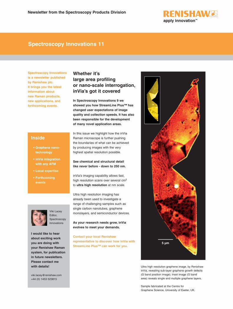
Newsletter from the Spectroscopy Products Division I would like to hear about exciting work you are doing with your Renishaw Raman system, for publication in future newsletters. Please contact me with details! [email protected] +44 (0) 1453 523815 Viki Lacey Editor, Spectroscopy Innovations Whether it’s large area profiling or nano-scale interrogation, inVia’s got it covered In Spectroscopy Innovations 9 we showed you how StreamLine Plus™ has changed user expectations of image quality and collection speeds. It has also been responsible for the development of many novel application areas. In this issue we highlight how the inVia Raman microscope is further pushing the boundaries of what can be achieved by producing images with the very highest spatial resolution possible. See chemical and structural detail like never before - down to 250 nm. inVia’s imaging capability allows fast, high resolution scans over several cm 2 to ultra high resolution at nm scale. Ultra high resolution imaging has already been used to investigate a range of challenging samples such as single carbon nanotubes, graphene monolayers, and semiconductor devices. As your research needs grow, inVia evolves to meet your demands. Contact your local Renishaw representative to discover how inVia with StreamLine Plus™ can work for you. Ultra high resolution graphene image, by Renishaw inVia, revealing sub-layer graphene growth defects (G band position image). Inset image (G band area) reveals single and multiple graphene layers. Sample fabricated at the Centre for Graphene Science, University of Exeter, UK. 5 µm Spectroscopy Innovations is a newsletter published by Renishaw plc. It brings you the latest information about new Raman products, new applications, and forthcoming events. Inside • Graphene nano- technology • inVia integration with any AFM • Local expertise • Forthcoming events Spectroscopy Innovations 11
Transcript of 11 ations v Inno y oscop Spectr
Newsletter from the Spectroscopy Products Division
I would like to hear
about exciting work
you are doing with
your Renishaw Raman
system, for publication
in future newsletters.
Please contact me
with details!
[email protected] +44 (0) 1453 523815
Viki Lacey Editor, Spectroscopy Innovations
Whether it’s large area profiling or nano-scale interrogation, inVia’s got it covered
In Spectroscopy Innovations 9 we
showed you how StreamLine Plus™ has
changed user expectations of image
quality and collection speeds. It has also
been responsible for the development
of many novel application areas.
In this issue we highlight how the inVia
Raman microscope is further pushing
the boundaries of what can be achieved
by producing images with the very
highest spatial resolution possible.
See chemical and structural detail
like never before - down to 250 nm.
inVia’s imaging capability allows fast,
high resolution scans over several cm2
to ultra high resolution at nm scale.
Ultra high resolution imaging has
already been used to investigate a
range of challenging samples such as
single carbon nanotubes, graphene
monolayers, and semiconductor devices.
As your research needs grow, inVia
evolves to meet your demands.
Contact your local Renishaw
representative to discover how inVia with
StreamLine Plus™ can work for you.
Ultra high resolution graphene image, by Renishaw inVia, revealing sub-layer graphene growth defects (G band position image). Inset image (G band area) reveals single and multiple graphene layers.
Sample fabricated at the Centre for Graphene Science, University of Exeter, UK.
5 µm
Spectroscopy Innovations
is a newsletter published
by Renishaw plc.
It brings you the latest
information about
new Raman products,
new applications, and
forthcoming events.
Inside
• Graphene nano-
technology
• inVia integration
with any AFM
• Local expertise
• Forthcoming
events
Spectroscopy Innovations 11

Newsletter from the Spectroscopy Products Division
Raman and atomic force microscopy (AFM)
Renishaw was the first to realise the
power of an integrated Raman/AFM
instrument. 1999 saw the first combination
of a Nanonics SPM with a Renishaw
Raman microscope at Chalmers
University of Technology, Sweden.
Professor Shen’s group at the National
University of Singapore soon followed;
this was the first true collaboration
of Renishaw with Nanonics Imaging
Ltd (Jerusalem, Israel). This ground-
breaking integration of the two companies’
instruments was awarded the prestigious
Photonics Circle of Excellence in 2002.
Since then Renishaw’s inVia has become
the Raman microscope of choice for
those wishing to combine the benefits
of AFM and Raman. Simultaneous
measurements are optimised by efficient
coupling of the laser directly to the AFM.
Dr Harold Chong of the University of
Southampton’s Nano Research Group
describes the integration between
the inVia Raman microscope with the
Nanonics MV4000 multiprobe AFM and
CryoView CV2000 as “flawless”. He also
highlights the direct optical coupling
between the instruments and states how
“the high efficiency Raman spectrometer
allows us to probe nanostructures
like quantum dots and nanowires to
extract vital material compositions”.
Further details about the University of
Southampton Nano Research Group's system
can be found here:
http://www.southampton-nanofab.com
/spmraman.php
Current applications of
Raman/AFM include:
• Life sciences
• Semiconductor
• Polymers
• Composite materials
• Data storage
• Novel materials for
electronics, display
and solar technology
• Quantum dots
and nanowires
• Carbon nanotubes
and graphene
• Pharmaceutical
Renishaw prides itself on innovation
and can count many ‘firsts’ in the fields
of engineering, metrology and Raman
spectroscopy. Renishaw identified
and pioneered the combination of
atomic force microscopy with Raman
scattering on a single platform and
now celebrates its 10th year supplying
combined Raman/AFM systems to the
research and academic communities.
The efficiency and stability at the core of
the inVia Raman microscope makes it the
perfect platform for integration with atomic
force microscopes (AFMs). Developed
in 1986 at IBM in Switzerland, the AFM
is a class of scanning probe microscope
(SPM). Very sharp tips made from materials
such as silicon, silicon nitride and glass
are scanned over a sample’s surface
with a very sensitive feedback loop to
record physical changes in the sample.
Crucially, the resolution of these instruments
lies in the nanometre range. Under certain
conditions, AFMs can achieve atomic
resolution. Raman spectroscopy provides the
perfect complement for AFM measurements
as it provides detailed chemical information
about the sample; something that is missing
from the array of imaging modes of AFMs.
Veeco BioScope II AFM coupled to an inVia Raman microscope.

The high efficiency Raman
spectrometer allows us
to probe nanostructures
like quantum dots and
nanowires to extract vital
material compositions”.
Dr Harold Chong, Nano Research Group, University of Southampton,UK.
One of the most exciting developments
in Raman spectroscopy has been TERS,
tip enhanced Raman scattering. And
here, Renishaw can claim another first. In
2001 Z.X. Shen and W.X. Sun published
TERS data from a semiconductor device.
The technique has evolved and a lateral
spatial resolution of 20 nm has been shown,
a significant improvement over conventional
far-field Raman measurements which are
limited by diffraction to around 250 nm. By
holding a specially-prepared sharp probe
a few nms from the sample’s surface in the
AFM, highly-localised enhanced Raman
signals can be generated by increasing
the strength of the electromagnetic field
through surface plasmons supported at
the apex of the tip. Etched gold wires, Ag-
and Au-coated Si and glass AFMs have
all been used to generate TERS signals.
The mechanism is analogous to SERS
(Surface Enhanced Raman Scattering)
but is confined to the region of tip/sample
interaction which can be as small as a few
nanometres. Dr Chong has used TERS to
identify the stress in SiGe semiconductors
“more clearly and accurately”. All
Renishaw’s integrations with AFMs are
suited to collecting TERS signals.
The inVia Raman microscope can now be
combined with instruments from all the major
vendors, realising the potential that their
products have to offer. Users of SPMs from
world leaders including Veeco, NT-MDT, and
JPK have all chosen to couple Renishaw's
inVia to their cutting-edge systems.
Physical measurements from the sample
determined from the AFM are collected
simultaneously with Raman spectra on one
platform so data can be directly correlated.
Contact your local Renishaw office to find out how combined Raman/AFM could help
you get in touch with your samples, or visit
http://www.renishaw.com/ramanafm for further information.
Raman shift / cm-1
Near-field (TERS)
Far-field
500 510 530520
Near-field (TERS) spectrum and far-field spectrum of strained Si on SiGe. The surface sensitivity of TERS exhibits more of the stressed surface Si component.
inVia Raman microscope with a Nanonics MV4000 AFM system housed in a custom acoustic enclosure.
An NT-MDT NTEGRA AFM system with direct optical coupling to an inVia Raman microscope.
“
The combination of
NTEGRA (NT-MDT) with
inVia (Renishaw) gives an
opportunity to obtain TERS
chemical images with a
very high spatial resolution
of the range of materials,
such as nanocomposites
and membranes,
carbon nanotubes and
graphene, to study
transport phenomena in
nanostructured membranes
and in biological samples”.
“
“Direct optical coupling of
NTEGRA with inVia system
provides reliability and
stability for the challenging
research with TERS. This,
combined with the relative
ease of use of inVia
system and expertise of
Renishaw, promotes our
confidence in performing
these experiments”.
Prof Sergei Kazarian, Imperial College London, UK.
© 2010 Renishaw plc. All rights reserved.RENISHAW® and the probe emblem used in the RENISHAW logo are registered trademarks of Renishaw plc in the UK and other countries. apply innovation is a trademark of Renishaw plc.
L-9836-3784-01-A January 2010
Renishaw, your local Raman company
One of the secrets of Renishaw’s success has
been a commitment to supporting customers with
local expertise, in their own local language.
Exports from the UK account for 93% of Renishaw’s
business: a testament to the success of our ‘local support’
initiative. Although English remains the most common
language used in the international scientific community,
customers appreciate advice and support that can be
understood by all people, at all levels of the organisation.
With over 50 wholly owned offices in 31 countries,
complemented by specialist agents in many other countries,
Renishaw can claim to have the Raman world covered!
We speak your language
This commitment to our customers is exemplified
by our website www.renishaw.com, which is
now available in 20 different language versions,
including Slovene, Russian, Turkish and both the
simplified and traditional Chinese scripts.
The creation and maintenance of these sites is a major
undertaking, but are part of our commitment to make it easy
to work with Renishaw, wherever you are in the world.
Flexibility and upgradeability from the only
Raman system you’ll ever need.
Contact your local Renishaw representative to discover
how Renishaw’s inVia speaks your language.
UKSPEC 2010 12 to 17 June
University of Manchester
Europe
Analytica 2010 23 to 26 March
Munich, Germany
Het Instruments 28 Sep to 1 Oct
Amsterdam, Netherlands
Asia
PV Expo 2010 3 to 5 March
Tokyo, Japan
Semicon 2010 2 to 4 December
Chiba, Japan
USA
Pittcon 2010 1 to 5 March
Orlando, Florida
SPIE 2010 5 to 9 April
Orlando, Florida
ICORS 2010 8 to 13 August
Boston, Massachusetts
2010 seminars and workshops
Renishaw will also be hosting a series of spectroscopy
seminars and workshops, focusing on the latest
innovations and combined technologies.
The first of these seminars will be held in the
Czech Republic on 27 January 2010.
For details of all forthcoming events, please visit our
website http://www.renishaw.com/ramanevents
We look forward to seeing you there!
2010 exhibitions and conferences
Every year Renishaw
attends a range of ‘premier’
events worldwide.
Please come and talk
to your local Renishaw
representative at one of
the following events.
Renishaw plcSpectroscopy Products DivisionOld Town, Wotton-under-Edge, Gloucestershire GL12 7DW United Kingdom
T +44 1453 524524 F +44 1453 523901 E [email protected]
www.renishaw.com/raman