1 Nano-Photolithography and an Introduction to Fabrication and Characterization of Plasmonic...
44
1 Nano-Photolithography and an Introduction to Fabrication and Characterization of Plasmonic Waveguides Hamid Nejati ELEC 527 Professor Tour, Professor Zhong 03/29/2007
-
Upload
eileen-shields -
Category
Documents
-
view
225 -
download
3
Transcript of 1 Nano-Photolithography and an Introduction to Fabrication and Characterization of Plasmonic...
1
Nano-Photolithography and an Introduction to Fabrication and Characterization of Plasmonic
Waveguides
Hamid Nejati
ELEC 527
Professor Tour, Professor Zhong
03/29/2007

2/44
Outline
Motivation and Introduction
Nano-photolithography
Excitation
Fabrication
Characterization
Conclusion

3/44
Motivation
Photolithography: Diffraction limit of light:
resolution >100nm Higher speed and
repeatable Lift off process
E-beam lithography: Higher resolution: around
20nm Lower speed and non
repeatable
Nano-imprint Industrial
Light
Photomask substrate
Laser light
Aqueous development
Chromium etch
Photoresist strip

4/44
Motivation
Photolithography (Mercury lamp) Diffraction limit of light
Plasmonics Sub wavelength operation
Y. Xia et al., “Soft lithography”, Angewandte Chemie International Edition, Vol. 37, pp. 550–575, 1998
~50 nm
Idea: Use near-field coupling between closely spaced metal nanoparticles or planar plasmonic waveguides for information propagation below the diffraction limit of light
5/44
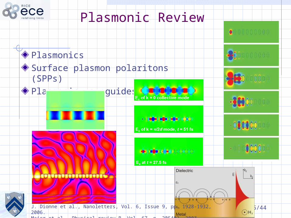
Plasmonic Review
Plasmonics
Surface plasmon polaritons (SPPs)
Plasmonic waveguides
J. Dionne et al., Nanoletters, Vol. 6, Issue 9, pp. 1928-1932, 2006.Maier et al., Physical review B, Vol. 67, p. 205402, 2003.

6/44
Comparing the plasmon printing to photolithography
Projection lithographysmallest feature size ~
Plasmon printingsmallest feature size ~0.1
PHOTORESIST
SUBSTRATE
MASK
410 nm
EXPOSE
DEVELOP
P. Kik et al., Mat. Res. Soc. Symp. Proc. Vol. 705, 2002

7/44
Field enhancement
Plasmon nano-sphere field profile
8/44
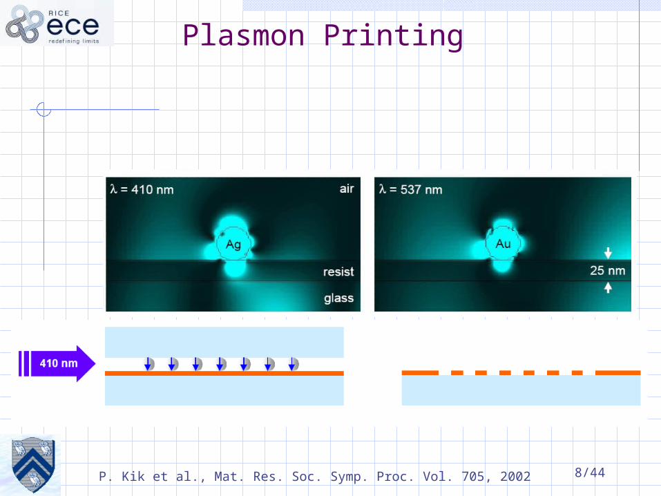
Plasmon Printing
P. Kik et al., Mat. Res. Soc. Symp. Proc. Vol. 705, 2002
9/44
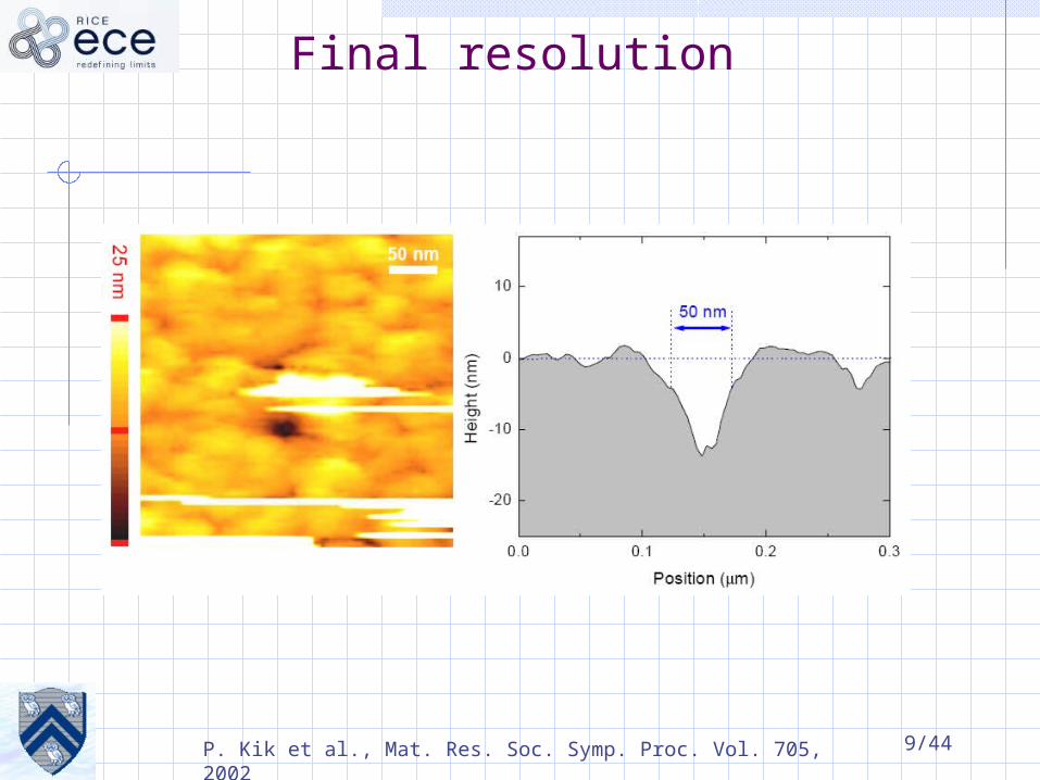
Final resolution
P. Kik et al., Mat. Res. Soc. Symp. Proc. Vol. 705, 2002

10/44
Plasmon Excitation
Plasmonic waves have bigger K vector in comparison to the light waves
Sources: He-Ne Laser (632.8 nm) Excimer laser 248nm Laser diode 1550nm
DielectricMetal
DielectricMetalSP KK
0

11/44
Excitation ideas
Trick1: excitation from a high index medium for surface plasmon at air/metal interface (prism)
Trick2: K vector in periodic structures due to Bloch theorem is not single (periodic with reciprocal lattice vector) (grating)

12/44
Excitation ideas
Trick3: excitation with dots
Trick4: array of dots
13/44
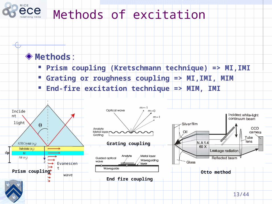
Methods of excitation
Methods: Prism coupling (Kretschmann technique) => MI,IMI Grating or roughness coupling => MI,IMI, MIM End-fire excitation technique => MIM, IMI
Incident
light
Evanescent
wave
dp
Prism coupling
Grating coupling
End fire coupling
Otto method

14/44
Prism coupling
Excitation of MI, IMI setups, and Asymmetric modeExcitation angle is dependent on the thickness of the filmCons:
Adjustment of gap separation & beam position, poor stability Expensive high-index prism and adjustment system
Pros: High efficiency and Selecting any guide mode (K-matching) Adjusting in experiment (detachable prism)
DielectricMetal
DielectricMetalKnSinK
Re00

15/44
Inherent Roughness of the Metal Film
Inherent roughness of the metal film acts as a statistically determined distribution of inelastic scatter centers for an SPP => scattered light method
Cons: Low intensity Inhomogeneous distribution
Sharp tip of microscope: tip scatters part of the local optical near field into the fiber and then to the photo detector.

16/44
End-Fire Coupling
Coupling with the direct excitation from the end of waveguide
Butt coupling of Polarization maintained fiber to the input and a single mode fiber at output
Optical index matched gel (OCF446 Nye optical)
Lens system and IR camera
Thermoelectric cooler
Tunable laser or EE-LED diode (1.55μm)+ polarization controller
Optical spectrum analyzer

17/44
Grating Coupling
Pros: High efficiency with optimum design Any guided mode can be excited Compact, stable, and inexpensive for Integration in waveguides
Cons: Complex theoretical calculation and advanced fabrication technique Device parameters can’t be adjusted after fabrication
Other Coupling methods Tapered coupling Prism-grating coupling Holographic coupling
Inherent roughness of filmWaveguide
Source
photodetector
grating grating

18/44
Grating coupling
Grating structure: coupling and shape
19/44
Corrugated surface
Perforated or imperforated surfaces can invert plasmon to light and light to plasmon (even the incident light from mercury lamp in photolithography)
Periodic structures like gratings have different values of K vector (As Bloch waves), which helps the coupling of light to plasmon.
Surface plasmon wavelength is proportional to the periodicity of the lattice

20/44
Interference pattern
Luo et al., Appl. Phys. Let., Vol. 84, No. 23, 2004.
Luo et al., Optics Express, Vol. 12, No. 14, 3055, 2004.
Resolution: 50nm

21/44
Superlens
Snell’s law
Negative refractive index (left handed material LH)
Subwavelength resolution
Source Image
Superlens
n=-1n=1 n=1
RH RHLH
22/44
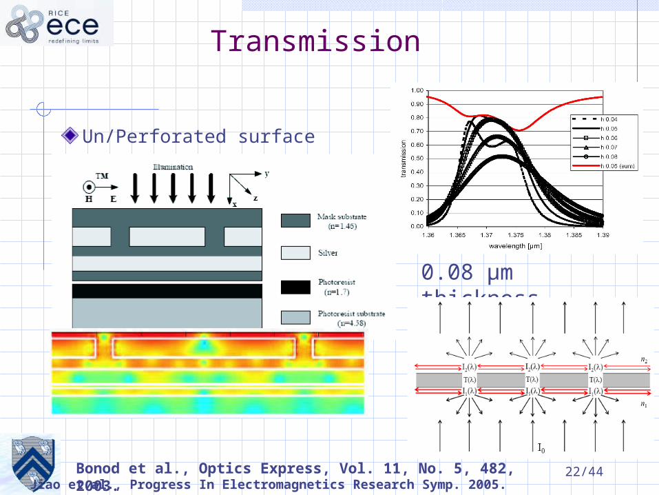
Transmission
Un/Perforated surface
Bonod et al., Optics Express, Vol. 11, No. 5, 482, 2003.
0.08 μm thickness
Jiao et al., Progress In Electromagnetics Research Symp. 2005.

23/44
Interference patterns
Luo et al., Optics Express, Vol. 12, No. 14, 2004.
Incident light: λ=436nm; E=2843mev
24/44
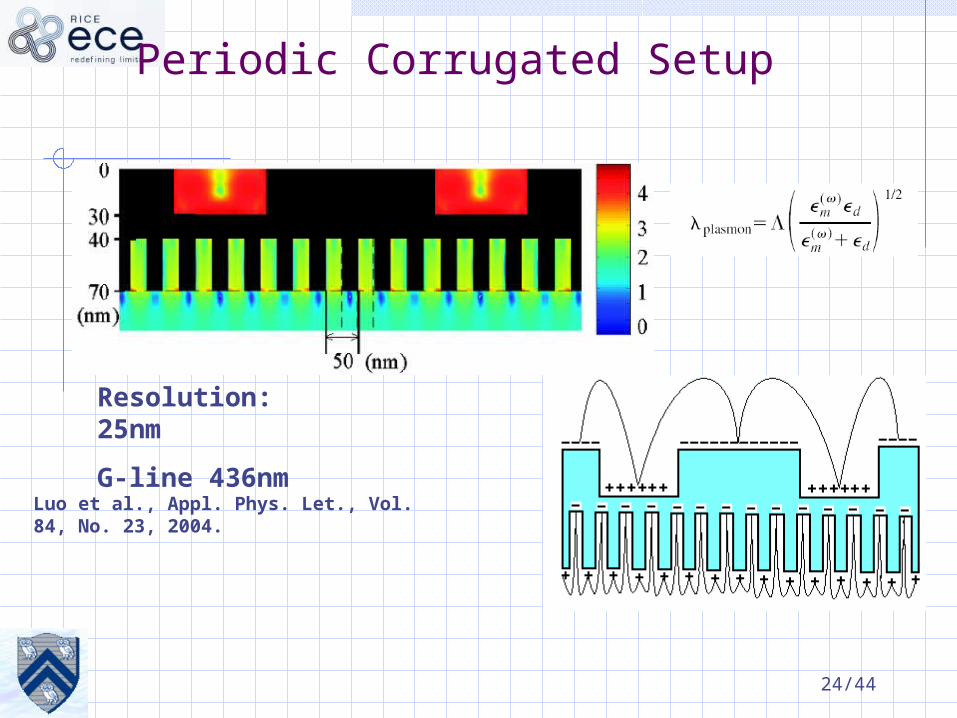
Periodic Corrugated Setup
Luo et al., Appl. Phys. Let., Vol. 84, No. 23, 2004.
Resolution: 25nm
G-line 436nm

25/44
Plasmonic structures
Planar structures Simple MI waveguide IMI waveguide MIM waveguide Bragg grating
Non-planar structures Nano-particle Nano-shell
I M M M MM I I I
Bragg grating
M I I I I II
Bragg gratingMIM
IMI
IM
Nano-shell Nano-sphereL. Hirish et al, PNAS, Vol. 100, No. 23, p. 13549, 2003.
26/44
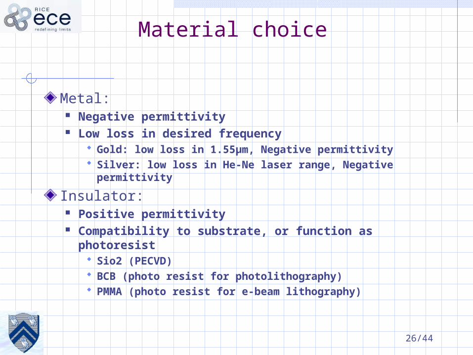
Material choice
Metal: Negative permittivity Low loss in desired frequency
Gold: low loss in 1.55μm, Negative permittivity Silver: low loss in He-Ne laser range, Negative permittivity
Insulator: Positive permittivity Compatibility to substrate, or function as photoresist
Sio2 (PECVD) BCB (photo resist for photolithography) PMMA (photo resist for e-beam lithography)

27/44
Substrate choice
Silicon substrate SOI substrate Oxidation Photoresist
Silica substrate Quartz Fused silica glass ITO: special usage for e-beam lithography, need
low conductance (Indium tin oxide coating)
ITO coated glass
Silicon substrate
Fused silica glass
Quartz substrate
28/44
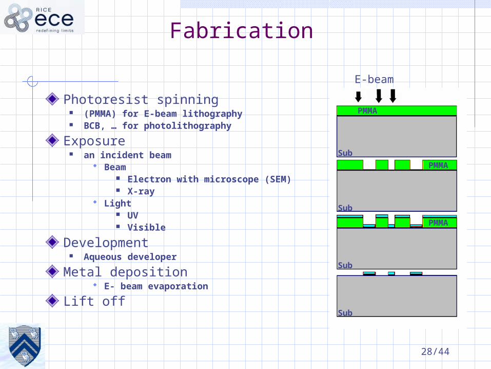
Fabrication
Photoresist spinning (PMMA) for E-beam lithography BCB, … for photolithography
Exposure an incident beam
Beam Electron with microscope (SEM) X-ray
Light UV Visible
Development Aqueous developer
Metal deposition E- beam evaporation
Lift off
E-beam
PMMA
PMMA
PMMA
Sub
Sub
Sub
Sub
29/44
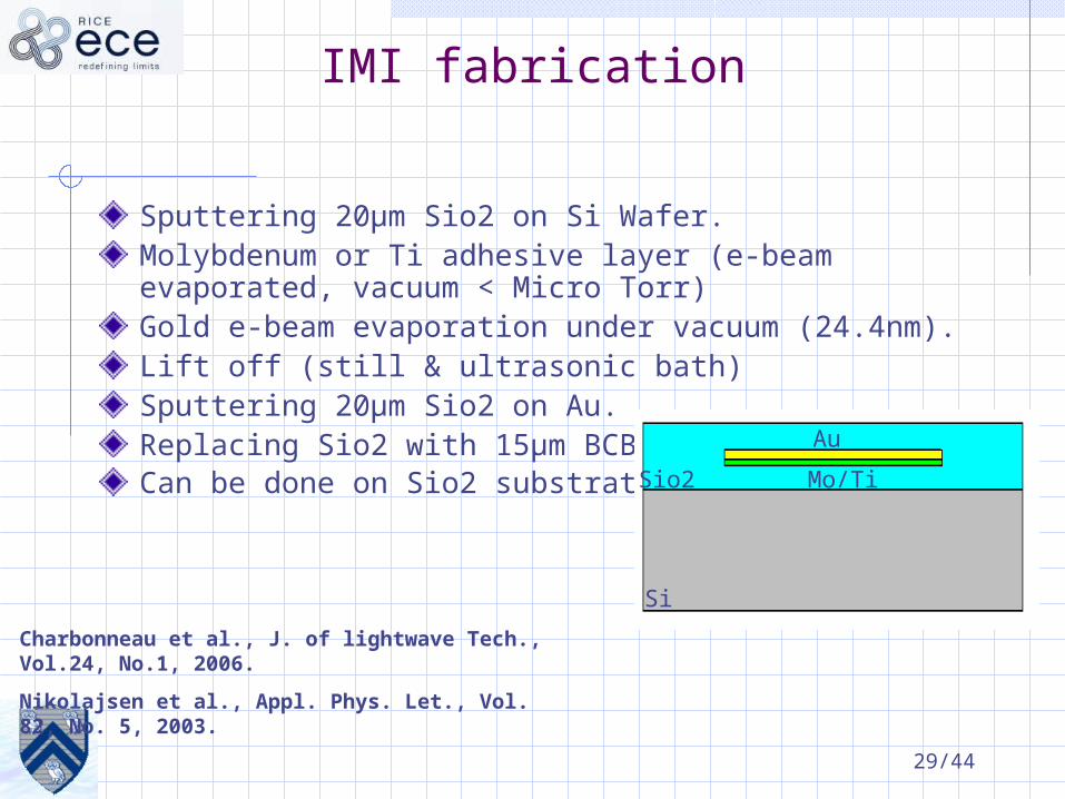
IMI fabrication
Sputtering 20μm Sio2 on Si Wafer.Molybdenum or Ti adhesive layer (e-beam evaporated, vacuum < Micro Torr) Gold e-beam evaporation under vacuum (24.4nm).Lift off (still & ultrasonic bath)Sputtering 20μm Sio2 on Au.Replacing Sio2 with 15μm BCB.Can be done on Sio2 substrate.
Charbonneau et al., J. of lightwave Tech., Vol.24, No.1, 2006.
Nikolajsen et al., Appl. Phys. Let., Vol. 82, No. 5, 2003.
Si
Sio2 Mo/Ti
Au

30/44
IMI FabricationCyclotene (20μm)Adhesion promoterSi wafer
UV light
Mask
+ photo resist (S1813)Cyclotene (20μm)Si wafer
undercut
+ photo resist (S1813)Cyclotene (20μm)
Si wafer
Gold+ photo resist (S1813)Cyclotene (20μm)Si wafer
Gold
Cyclotene (20μm)
Si wafer
Cyclotene
Gold
Cyclotene
Si wafer
10-20nm
•Spin coat adhesion promoter (AP3000) and cyclotene @ 1000rpm(10s) and 2000rpm(30s)
•Soft bake @ 210 (10min) + hard bake @ 250 (10min)
•Spin coat shipley1813 photoresist @ 4000rpm(30s)
•Pre bake @ 115 (10min) expose (karl-suss MJB3 mask aligner) soak sample in chlorobenzene (10min)
•Develop microposit MF-319 (2min) => undercut => prevent the metal to be coated on side walls=> increase the lift off quality
•Deposit 20nm gold with e-beam evaporation
•Acetone rinsing+ lift off+ isopropanol rinsing
•Spin coat cyclotene + pre and post bake
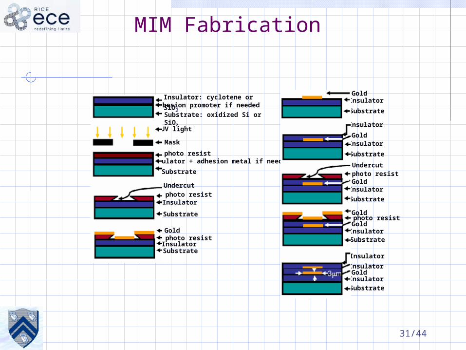
31/44
Substrate: oxidized Si or SiO2
Insulator: cyclotene or SiO2
Insulator + adhesion metal if needed
Adhesion promoter if needed
UV light
Mask
+ photo resist
Substrate
Undercut
+ photo resist Insulator
Substrate
Gold
Substrate
Insulator+ photo resist
Substrate
Substrate
Substrate
Substrate
Substrate
Insulator
Insulator
Insulator
Insulator
Insulator
Gold
Gold
Gold
Gold
Gold
Insulator
Insulator
InsulatorGold
+ photo resist
+ photo resist
Undercut
MIM Fabrication
32/44
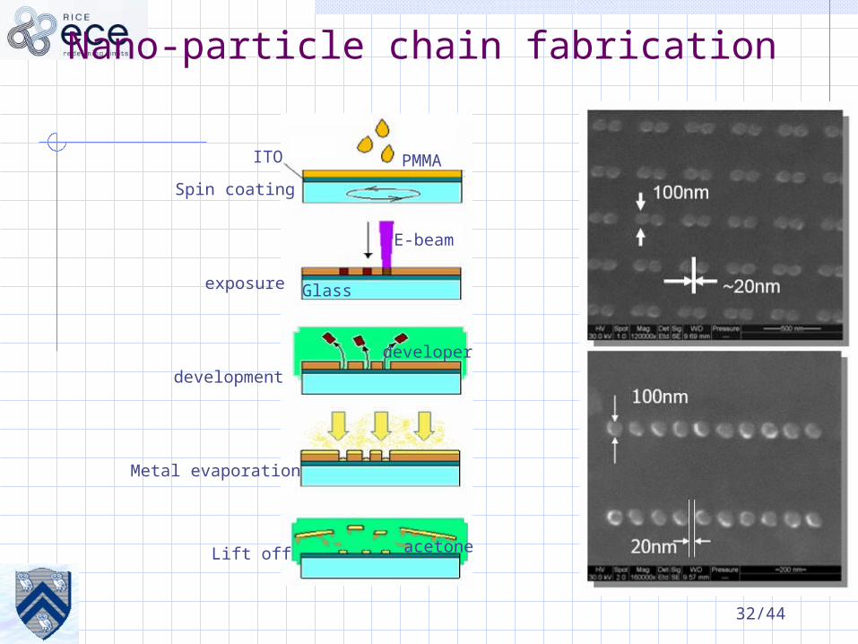
Nano-particle chain fabrication
PMMAITO
Glass
developer
acetone
E-beam
Spin coating
exposure
Lift off
Metal evaporation
development

33/44
MIM fabrication
Au deposition on fused silica substrate by magnetron sputtering (150nm)
Sio2 PECVD (3.3nm, 56nm, 14nm)
No annealing + cleaving
Au deposition on fused silica substrate by magnetron sputtering (150nm)
Covered by Sio2 or air
Miyazaki et al., Phys. Rev. Let., PRL 96, 097401, 2006

34/44
Bragg grating
Photoresist spin coating Pre baka Post bake
Patterning lithography
Etching KOH Enchants
Au deposition E-beam evaporation
35/44
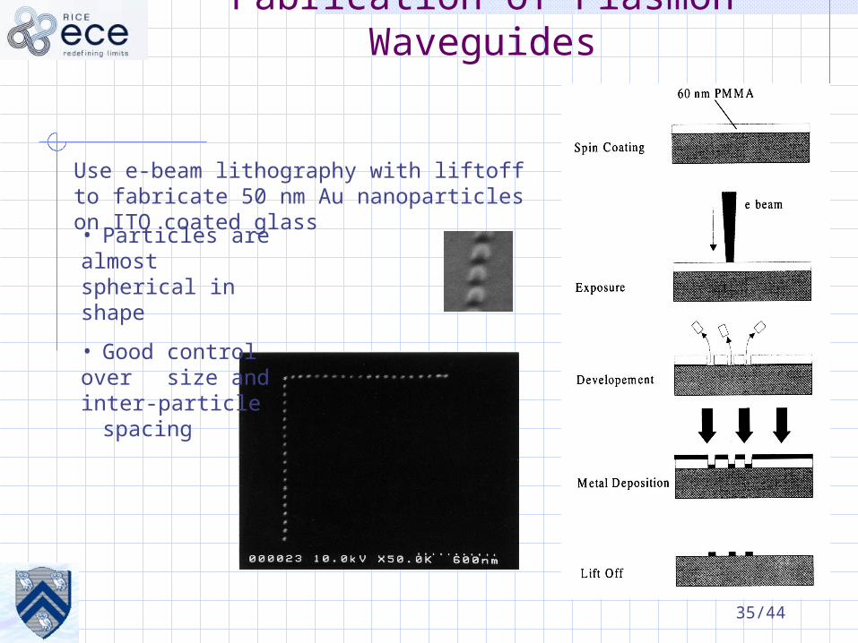
Fabrication of Plasmon Waveguides
Use e-beam lithography with liftoff to fabricate 50 nm Au nanoparticles on ITO coated glass
• Particles are almost spherical in shape
• Good control over size and inter-particle spacing

36/44
Characterization of Metallic Nanoparticle Waveguide and Fabrication of Nanoshell
NSOM excitationFar field detectionFabrication methods:
Silica sphere: stober method, std < 5%
Surface modification: APTMS Attachment of gold nanoparticle (1-
2nm) Reductive growth of thin gold shell
NSOM excitation
NSOM characterization
37/44
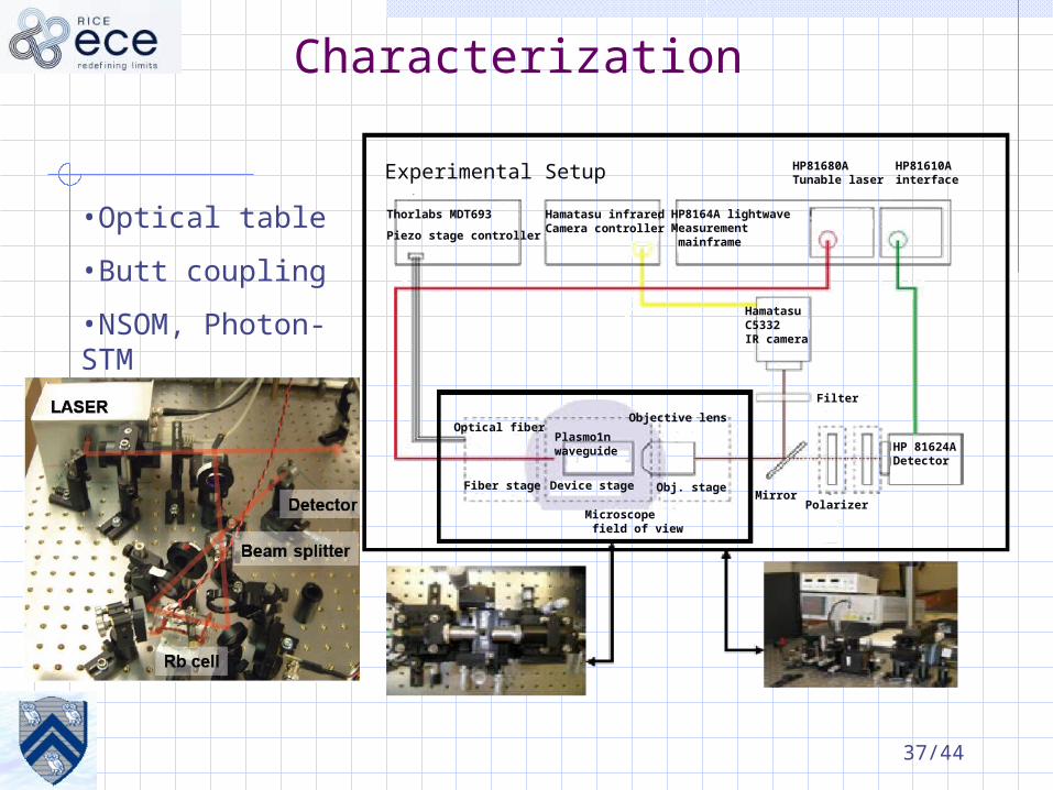
Characterization
Experimental Setup
Thorlabs MDT693
Piezo stage controller
Hamatasu infraredCamera controller
HP8164A lightwaveMeasurement mainframe
HP81680ATunable laser
HP81610Ainterface
HP 81624ADetector
HamatasuC5332IR camera
MirrorPolarizer
Microscope field of view
Obj. stageDevice stageFiber stage
Plasmo1n waveguide
Objective lensOptical fiber
Filter
•Optical table
•Butt coupling
•NSOM, Photon-STM

38/44
Methods of characterization
Near field probing
Fluorescence imaging
Light scattering from surface roughness
Fourier domain observation of scattering in a grating array
Optical spectroscopy
NSOM
PSTM
Leakage radiation microscopy

39/44
Transmission loss
Cut-back method
Prism sliding method
Scattering detection method
Lens Lens
Photodetector
cutting
Waveguide
Prism Prism
Matching liquidWaveguide
Photodetector
Sliding <------
Prism
waveguide
Scanning
Fiber probe
PhotodetectorLock-in amplifier
recorder

40/44
NSOM
Aperture near field scanning optical microscopy
Aperture less NSOM

41/44
NSOM
Multi-application 4 probe NSOM, AFM,SPM,…

42/44
NSOM
43/44
Conclusion
Plasmon assisted Nanophotolithography was reviewed
Fabrication, Excitation, and characterization of a plasmonic waveguide is reviewed
Special methods for characterization of MI, MIM, IMI, and Grating setups understood

44/44
Thank you