
1. Explain in detail memory classification.[Summer-2016, Summer … · 2019. 11. 19. · Unit–IV...
19
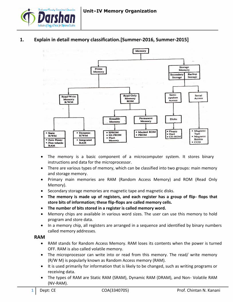
Unit–IV Memory Organization 1 Dept: CE COA(3340705) Prof. Chintan N. Kanani 1. Explain in detail memory classification.[Summer-2016, Summer-2015] The memory is a basic component of a microcomputer system. It stores binary instructions and data for the microprocessor. There are various types of memory, which can be classified into two groups: main memory and storage memory. Primary main memories are RAM (Random Access Memory) and ROM (Read Only Memory). Secondary storage memories are magnetic tape and magnetic disks. The memory is made up of registers, and each register has a group of flip- flops that store bits of information; these flip-flops are called memory cells. The number of bits stored in a register is called memory word. Memory chips are available in various word sizes. The user can use this memory to hold program and store data. In a memory chip, all registers are arranged in a sequence and identified by binary numbers called memory addresses. RAM RAM stands for Random Access Memory. RAM loses its contents when the power is turned OFF. RAM is also called volatile memory. The microprocessor can write into or read from this memory. The read/ write memory (R/W M) is popularly known as Random Access memory (RAM). It is used primarily for information that is likely to be changed, such as writing programs or receiving data. The types of RAM are Static RAM (SRAM), Dynamic RAM (DRAM), and Non- Volatile RAM (NV-RAM).
Transcript of 1. Explain in detail memory classification.[Summer-2016, Summer … · 2019. 11. 19. · Unit–IV...
Unit–IV Memory Organization
1 Dept: CE COA(3340705) Prof. Chintan N. Kanani
1. Explain in detail memory classification.[Summer-2016, Summer-2015]
The memory is a basic component of a microcomputer system. It stores binary instructions and data for the microprocessor.
There are various types of memory, which can be classified into two groups: main memory and storage memory.
Primary main memories are RAM (Random Access Memory) and ROM (Read Only Memory).
Secondary storage memories are magnetic tape and magnetic disks.
The memory is made up of registers, and each register has a group of flip- flops that store bits of information; these flip-flops are called memory cells.
The number of bits stored in a register is called memory word.
Memory chips are available in various word sizes. The user can use this memory to hold program and store data.
In a memory chip, all registers are arranged in a sequence and identified by binary numbers called memory addresses.
RAM RAM stands for Random Access Memory. RAM loses its contents when the power is turned
OFF. RAM is also called volatile memory.
The microprocessor can write into or read from this memory. The read/ write memory (R/W M) is popularly known as Random Access memory (RAM).
It is used primarily for information that is likely to be changed, such as writing programs or receiving data.
The types of RAM are Static RAM (SRAM), Dynamic RAM (DRAM), and Non- Volatile RAM (NV-RAM).
Unit–IV Memory Organization
2 Dept: CE COA(3340705) Prof. Chintan N. Kanani
ROM ROM stands for Read Only Memory. ROM does not lose its contents when the power is
turned OFF. ROM is also called non-volatile memory.
The microprocessor can only read from this memory.
The types of ROM are masked ROM, PROM, EPROM, EEPROM and Flash Memory.
Masked ROM In this ROM, a bit pattern is permanently recorded by the masking and metallization
process.
Memory manufacturers are generally equipped to do this process. It is an expensive and specialized process, but economical for large production quantities.
PROM PROM stands for Programmable Read Only Memory.
This memory has nichrome or poly-silicon wires arranged in a matrix; these wires can be functionally viewed as diodes or fuses.
This memory can be programmed by the user with a special PROM programmer that selectively bums the fuses according to the bit pattern to be stored.
The process is known as “burning the PROM,” and the information stored is permanent.
EPROM EPROM stands for Erasable Programmable Read Only Memory.
This memory stores a bit by charging the floating gate of an field effect transistor.
Information is stored by using an EPROM programmer, which applies high voltages to charge the gate.
All the information can be erased by exposing the chip to ultraviolet light through its quartz window, and the chip can be reprogrammed.
Because the chip can be reused many times, this memory is ideally suited for product development, experimental projects, and college laboratories.
The disadvantages of EPROM are
1. It must be taken out of the circuit to erase it.
2. The entire chip must be erased.
3. The erasing process takes 15 to 20 minutes.
EE-PROM EPROM stands for Electrically Erasable Programmable Read Only Memory.
This memory is functionally similar to EPROM, except that information can be changed by using electrical signals at the register level rather than erasing all the information.
This has an advantage in field and remote control applications.
If EE-PROMs are used in the systems, they can be updated from a central computer by using a remote link via telephone lines.
Similarly, in a process control where timing information needs to be changed, it can be changed by sending electrical signals from a central place.
This memory also includes a Chip Erase mode, whereby the entire chip can be erased in 10 ms.

Unit–IV Memory Organization
3 Dept: CE COA(3340705) Prof. Chintan N. Kanani
This memory is expensive compared to EPROM or flash memory.
Flash Memory This is a variation of EE-PROM that is becoming popular. The major difference between the
flash memory and EE-PROM is in the erase procedure.
The EE-PROM can be erased at a register level, but the flash memory must be erased either entire level or at the sector (block) level.
These memory chips can be erased and programmed at least a million times.
The power supply requirement for programming these-chips was 12V, but now chips are available that can be programmed using a supply as low as 1.8 V. Therefore, this memory is ideally suited for low power systems.
2. Explain in detail Main memory.[Winter-2015, Summer-2015,Summer-2014] The main memory is the central storage unit in a computer system.
It is a relatively large and fast memory used to store programs and data during the computer operation.
The principal technology used for the main memory is based on semiconductor integrated circuits.
RAM This memory is volatile, meaning that when the power is turned off, all the contents are
destroyed. User can store his program as well as data inside this.
RAM is used for storing the bulk of the programs and data that are subject to change.
CS WR CS
0 x NONE
1 0 READ SELECTED WORD
1 1 WRITE SELECTED WORD
A Chip Select, CS, enables or disables the RAM.
ADRS specifies the address or location to read from or write to.
WR selects between reading from and writing to the memory. o To read from memory, WR should be set to 0. o OUT will be the n-bit value stored at ADRS. o To write to memory, we set WR = 1. o DATA is the n-bit value to save in memory.
There are k-address lines, which can specify one of 2k addresses
Each address contains an n-bit word.
Unit–IV Memory Organization
4 Dept: CE COA(3340705) Prof. Chintan N. Kanani
Types of RAM 1. SRAM- Static Random Access Memory 2. DRAM- Dynamic Random Access Memory
a. FP- Fast Page RAM b. EDO- Extended Data Output c. SDRAM- Synchronous DRAM
SRAM The static RAM is easier to use and has shorter read and write cycles.
The static RAM consists of internal flip-flops that store the binary information. The stored information remains valid as long as power is applied to the unit.
The SRAM are low density, high power, expensive and fast in operation.
All computer memory modules used in today’s computers are of the SRAM type. DRAM
The dynamic RAM stores the binary information in the form of electric charges that are applied to capacitors.
It is a refreshing type memory. As long as power is maintained on the memory modules the DRAM will hold its information.
The content of DRAM memory disappears from the memory within milliseconds, so in order to maintain its data it has to be refreshed periodically.
This makes the DRAM memory much slower than the SRAM. The computer memories you usually see are a form of DRAM, like SDRAM and DDR- SDRAM.
The capacitors are provided inside the chip by MOS transistors. The stored charge on the capacitors tends to discharge with time and the capacitors must be periodically recharged by refreshing the dynamic memory.
The DRAM offers reduced power consumption and larger storage capacity in a single memory chip.
ROM
ROM stands for Read Only Memory.
ROM is used for storing programs that are permanently resident in computer and for look-up tables..
The ROM portion of main memory is needed for storing an initial program called a BOOTSTRAP LOADER.
The bootstrap loader is program whose function is to start the computer software operating when power is turned on.
When the power is turned on, the hardware of the computer sets the program counter to the first address of the bootstrap loader.
The bootstrap programs load a portion of the operating system, from disk to main memory and control is then transferred to the operating system, which prepares the computer for general use.
Types of ROM 1. PROM- Programmable Read Only Memory 2. EPROM- Erasable Programmable Read Only Memory 3. EEPROM- Electrically Erasable Programmable Read Only Memory
Unit–IV Memory Organization
5 Dept: CE COA(3340705) Prof. Chintan N. Kanani
3. Explain in detail Memory Interfacing, Memory Organization, Memory Decoding logic, Memory speed
Memory Interfacing
The number of bits that a semiconductor memory chip can store is called chip capacity. It can be in units of Kb (Kilobits), Mb (megabits), Gb (Gigabits) and so on.
Memory organization
Memory chips are organized into a number of locations within the IC. Each location can hold 1 bit, 4 bits, 8 bits or even 16 bits, depending on how it is designed internally.
The number of bits that each location within the memory chip can hold is always equal to the number of data pins on the chip.
The total number of bits that a memory chip can store is equal to the number of locations times the number of data bits per location.
Memory Decoding Logic
Memory chip can be selected by equation- 2n = N Where, n= number of address lines, N=memory size.
Memory Speed
One of the most important characteristics of a memory chip is the speed at which its data can be accessed.
To access the data, the address is presented to the address pins, the READ pin is activated, and after a certain amount of time has elapsed, the data shows up at the data pins.
The speed of the memory chip is commonly referred to as its access time. The access time of memory chips varies from a few nanoseconds to hundreds of nanoseconds, depending on the IC technology used in the design and fabrication process.
4. Example:- A micro computer system use a RAM chip of 1K X 8 and ROM chip of 2K X 8 size. The system needs 4K RAM and 8K ROM.
1. How many RAM and ROM chips are required? 2. How many address lines needed to decode for RAM and ROM chips? 3. Write the memory address map for the microprocessor.
1. How many RAM and ROM chips are required? Given that, Size of single RAM chip is 1k X 8 or 1K Required size of RAM chip is 4 KB Number of RAM chips required = 4K X 8 1K X 8 = 4 chips Size of single ROM chip is 2K X 8 Required size of ROM chip is 8 KB Number of ROM chips required = 8K X 8 2K X 8 =4 chips
Unit–IV Memory Organization
6 Dept: CE COA(3340705) Prof. Chintan N. Kanani
2. How many address lines needed to decode for RAM and ROM chips? Number of address lines for RAM chip = log2 1K = log2 (2
0 x 210)
= 10 log2 2 = 10 address lines Number of address lines for ROM chip = log2 2K = log2 (2
1 x 210)
= log2 211 = 11 address lines
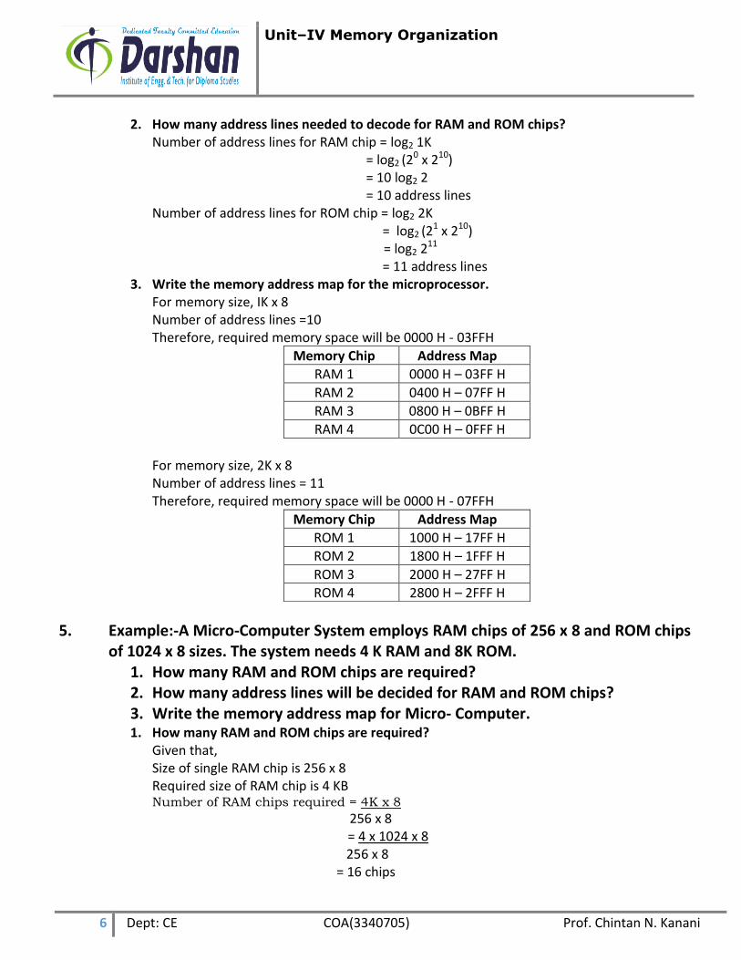
3. Write the memory address map for the microprocessor. For memory size, IK x 8 Number of address lines =10 Therefore, required memory space will be 0000 H - 03FFH
Memory Chip Address Map
RAM 1 0000 H – 03FF H
RAM 2 0400 H – 07FF H
RAM 3 0800 H – 0BFF H
RAM 4 0C00 H – 0FFF H
For memory size, 2K x 8 Number of address lines = 11 Therefore, required memory space will be 0000 H - 07FFH
Memory Chip Address Map
ROM 1 1000 H – 17FF H
ROM 2 1800 H – 1FFF H
ROM 3 2000 H – 27FF H
ROM 4 2800 H – 2FFF H
5. Example:-A Micro-Computer System employs RAM chips of 256 x 8 and ROM chips of 1024 x 8 sizes. The system needs 4 K RAM and 8K ROM.
1. How many RAM and ROM chips are required? 2. How many address lines will be decided for RAM and ROM chips? 3. Write the memory address map for Micro- Computer.
1. How many RAM and ROM chips are required? Given that, Size of single RAM chip is 256 x 8 Required size of RAM chip is 4 KB Number of RAM chips required = 4K x 8
256 x 8 = 4 x 1024 x 8 256 x 8 = 16 chips
Unit–IV Memory Organization
7 Dept: CE COA(3340705) Prof. Chintan N. Kanani
Size of single ROM chip is 1024 x 8 Required size of ROM chip is 8 KB Number of ROM chips required =4K x 8 256 x 8
= 8 x 1024 x 8 1024 x 8 = 8 chips
2. How many address lines will be decided for RAM and ROM chips? Number of address lines for RAM chip = log2 256 = log2 (2
8 )
= 8 log2 2 = 8 address lines Number of address lines for ROM chip = log2 1024 = log2 (2
10)
= 10 log2 2 = 10 address lines
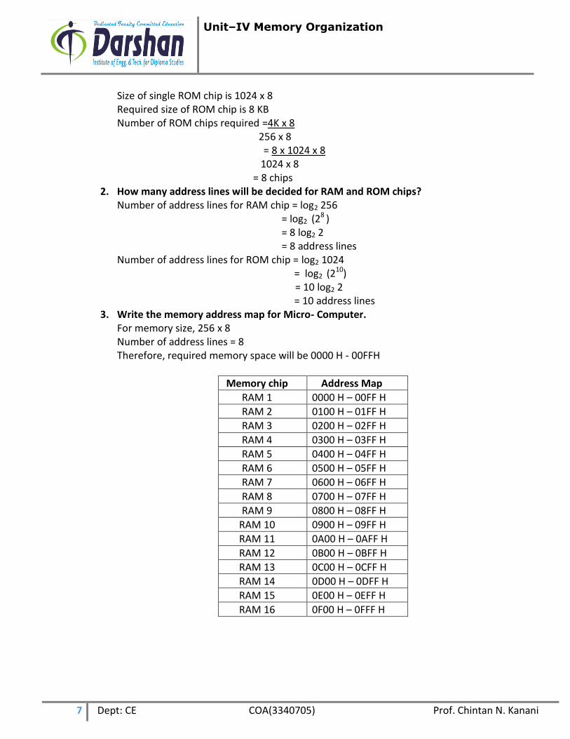
3. Write the memory address map for Micro- Computer. For memory size, 256 x 8 Number of address lines = 8 Therefore, required memory space will be 0000 H - 00FFH
Memory chip Address Map
RAM 1 0000 H – 00FF H
RAM 2 0100 H – 01FF H
RAM 3 0200 H – 02FF H
RAM 4 0300 H – 03FF H
RAM 5 0400 H – 04FF H
RAM 6 0500 H – 05FF H
RAM 7 0600 H – 06FF H
RAM 8 0700 H – 07FF H
RAM 9 0800 H – 08FF H
RAM 10 0900 H – 09FF H
RAM 11 0A00 H – 0AFF H
RAM 12 0B00 H – 0BFF H
RAM 13 0C00 H – 0CFF H
RAM 14 0D00 H – 0DFF H
RAM 15 0E00 H – 0EFF H
RAM 16 0F00 H – 0FFF H
Unit–IV Memory Organization
8 Dept: CE COA(3340705) Prof. Chintan N. Kanani
For memory size, 1024 x 8 Number of address lines = 10 Therefore, required memory space will be 0000 H - 03FFH
Memory Chip Address Map
ROM 1 1000 H – 13FF H
ROM 2 1400 H – 17FF H
ROM 3 1800 H – 1BFF H
ROM 4 1C00 H – 1FFF H
ROM 5 2000 H – 23FF H
ROM 6 2400H – 27FF H
ROM 7 2800 H – 2BFF H
ROM 8 2C00H – 2FFF H
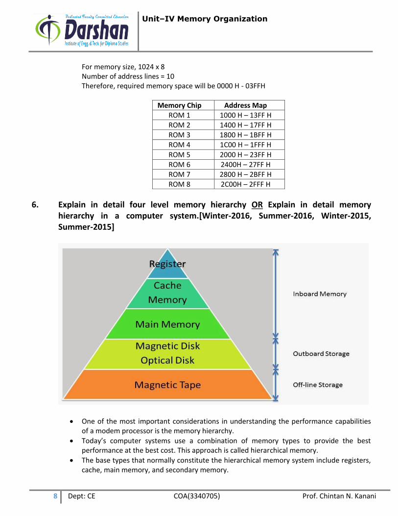
6. Explain in detail four level memory hierarchy OR Explain in detail memory hierarchy in a computer system.[Winter-2016, Summer-2016, Winter-2015, Summer-2015]
One of the most important considerations in understanding the performance capabilities of a modem processor is the memory hierarchy.
Today’s computer systems use a combination of memory types to provide the best performance at the best cost. This approach is called hierarchical memory.
The base types that normally constitute the hierarchical memory system include registers, cache, main memory, and secondary memory.
Unit–IV Memory Organization
9 Dept: CE COA(3340705) Prof. Chintan N. Kanani
Most general-purpose computers would run more efficiently if they were equipped with additional storage beyond the capacity of the main memory.
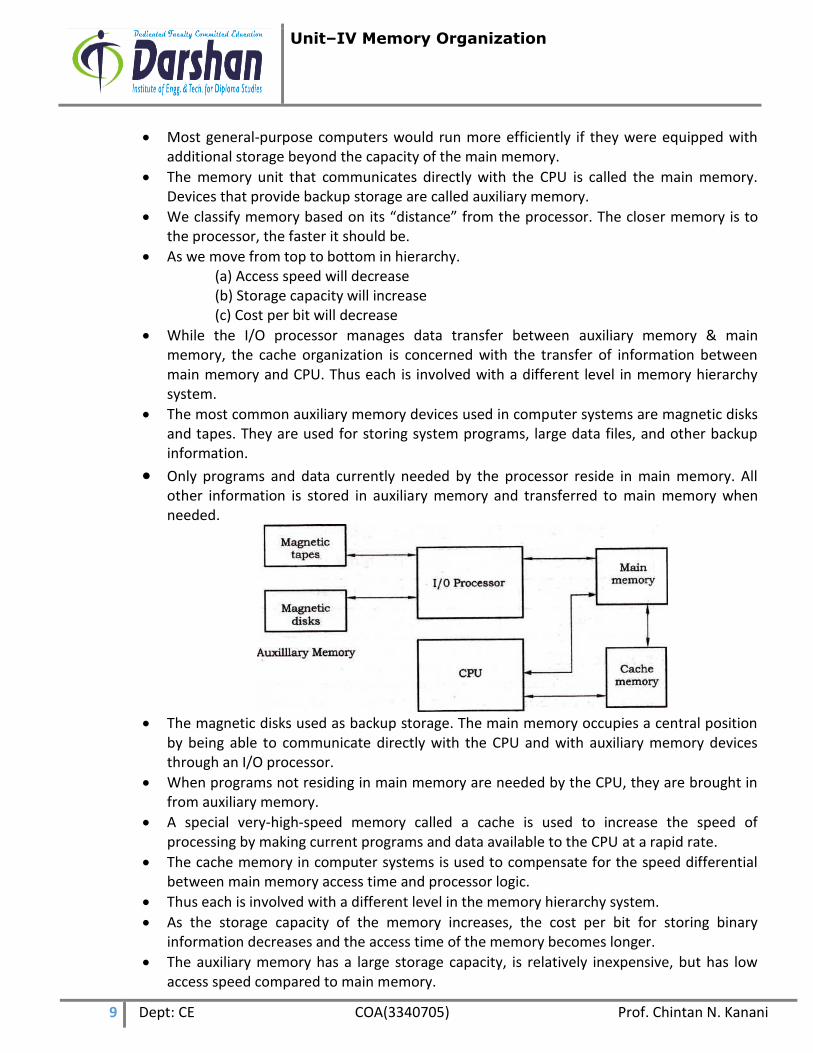
The memory unit that communicates directly with the CPU is called the main memory. Devices that provide backup storage are called auxiliary memory.
We classify memory based on its “distance” from the processor. The closer memory is to the processor, the faster it should be.
As we move from top to bottom in hierarchy. (a) Access speed will decrease (b) Storage capacity will increase (c) Cost per bit will decrease
While the I/O processor manages data transfer between auxiliary memory & main memory, the cache organization is concerned with the transfer of information between main memory and CPU. Thus each is involved with a different level in memory hierarchy system.
The most common auxiliary memory devices used in computer systems are magnetic disks and tapes. They are used for storing system programs, large data files, and other backup information.
Only programs and data currently needed by the processor reside in main memory. All other information is stored in auxiliary memory and transferred to main memory when needed.
The magnetic disks used as backup storage. The main memory occupies a central position
by being able to communicate directly with the CPU and with auxiliary memory devices through an I/O processor.
When programs not residing in main memory are needed by the CPU, they are brought in from auxiliary memory.
A special very-high-speed memory called a cache is used to increase the speed of processing by making current programs and data available to the CPU at a rapid rate.
The cache memory in computer systems is used to compensate for the speed differential between main memory access time and processor logic.
Thus each is involved with a different level in the memory hierarchy system.
As the storage capacity of the memory increases, the cost per bit for storing binary information decreases and the access time of the memory becomes longer.
The auxiliary memory has a large storage capacity, is relatively inexpensive, but has low access speed compared to main memory.

Unit–IV Memory Organization
10 Dept: CE COA(3340705) Prof. Chintan N. Kanani
The cache memory is very small, relatively expensive, and has very high access speed.
The overall goal of using a memory hierarchy is to obtain the highest- possible average access speed while minimizing the total cost of the entire memory system.
Advantages of memory Hierarchy : o Decrease frequency of accesses to slow memory o Decrease cost/bit o Improve average access time o Increase capacity
7. Explain in detail Auxiliary Memory. [Winter-2016] The most common auxiliary memory devices used in computer systems are magnetic disks
and tapes.
The important characteristics of any device are its access mode, access time, transfer rate, capacity, and cost.
The average time required to reach a storage location in memory and obtain its contents is called the access time.
A transfer time required to transfer data to or from the device.
The transfer rate is the number of characters or words that the device can transfer per second) sifter it has been positioned at the beginning of the record.
Magnetic Disks A magnetic disk is a circular plate constructed of metal or plastic coated with magnetized
material.
Both sides of the disk are used and several disks may be stacked on one spindle with read/write heads available on each surface.
All disks rotate together at high speed and are not stopped or started for access purposes.
Bits are stored in the magnetized surface in spots along concentric circles called tracks.
The tracks are commonly divided into sections called sectors.
The subdivision of one disk surface into tracks and sectors. Some units use a single RD/WR head for each disk surface. In another disk system separate RD/WR heads are provided for each track in each surface.

Unit–IV Memory Organization
11 Dept: CE COA(3340705) Prof. Chintan N. Kanani
Types of Magnetic Disk 1. Floppy disk A disk drive with removable disks is called a floppy disk. Disk drives for floppy disks are called
floppy drives.
Floppy disks are slower to access than hard disks and have less storage capacity, but they are much less expensive. And most importantly, they are portable.
The disks used with a floppy disk drive are small removable disks made of plastic coated with magnetic recording material.
Types of Floppies There are two sizes commonly used, with diameters of 51/4 and 31/2 inches. The 31/2 inch disks are smaller and can store more data than can the 51/4 inch disks.
51/4- inch:- This type of floppy is generally capable of storing between 100K and 1.2MB of data. The most common sizes are 360K and 1.2MB.
31/2 - inch:- small size, microfloppies have a larger storage capacity. The most common size is 1.44MB high-density.
2. Hard disk Disks that are permanently attached to the unit assembly and cannot be removed by the
occasional user are called hard disks.
A hard disk commonly known as a HDD (hard disk drive). It is a non-volatile storage device which stores digitally encoded data on rapidly rotating
platters with magnetic surfaces.
The storage capacity of a disk depends on the bits per inch of track and the tracks per inch of surface.
3. Magnetic tape Magnetic tape is a non-volatile storage medium consisting of a magnetic coating on a thin
plastic strip.
Nearly all recording tape is of this type, whether used for video, audio storage or general purpose digital data storage using a computer.
It is used mainly for secondary storage.
Most magnetic tape units are capable of reading and writing in several different densities.
8. Explain in detail Associative Memory OR explain in detail block diagram of associative memory.[Summer-2015,Summer-2014]
Many data-processing applications require the search of items in a table stored in memory.
The search procedure is a strategy for choosing ‘a sequence of addresses, reading the content of memory at each address, and comparing the information read with the item being searched until a match occurs.
The number of accesses to memory depends on the location of the item and the efficiency of the search algorithm.

Unit–IV Memory Organization
12 Dept: CE COA(3340705) Prof. Chintan N. Kanani
A memory unit accessed by content is called an associative memory or content addressable memory (CAM). This type of memory is accessed simultaneously and in parallel on the basis of data content rather than by specific address or location.
It consists of a memory array and logic for m words with n bits per word.
The argument register A and key register K each have n bits, one for each bit of a word,
The match register M has m bits, one for each memory word.
Each word in memory is compared in parallel with the content of the argument register.
The words that match the bits of the argument register set a corresponding bit in the match register.
After the matching process, those bits in the match register that have been set indicate the fact that their corresponding words have been matched.
The key register provides a mask for choosing a particular field or key in the argument word.
The entire argument is compared with each memory word if the key register contains all 1’s.
Otherwise, only those bits in the argument that have 1’s in their corresponding position of the key register are compared.
Thus the key provides a mask or identifying piece of information which specifies how the reference to memory is made.
9. Write short note on cache memory. OR Explain Principle of Locality of Reference with reference to Cache Memory. OR Explain Cash Memory with its hit ratio and mappings. OR Describe one architectural method to implement cache memory.[Winter-2016, Summer-2016, Winter-2015, Summer-2015, Summer-2014]
A cache memory is a small, temporary, but fast memory that the processor uses for information it is likely to need again in the very near future.
Cache is small or modestly sized memories typically 128KB, 256KB which are placed in between a CPU and memory, and run at speeds similar to CPU registers.
Instructions and data which are accessed are stored in this cache, so that subsequent accesses can find these instructions or data in the cache, rather than memory.
Because the cache is of a similar speed to a register, very little time is lost if the instruction
Unit–IV Memory Organization
13 Dept: CE COA(3340705) Prof. Chintan N. Kanani
or data is already in the cache. The cache memory Access time is less than the access time of main memory. The cache is
the fastest component in the memory hierarchy.
Operation of the Cache memory The basic operation of the cache is as follows. When the CPU needs to access memory, the
cache is examined.
If the word is found in the cache, it is read from the fast memory.
If the word addressed by the CPU is not found in the cache, the main memory is accessed to read the word.
A block of words is transferred from main memory to cache memory.
The block size may vary from one word to about 16 words.
In this manner, some data are transferred to cache so that future references to memory find the required words in the fast cache memory.
Performance Parameters of Cache Memory [Summer-2016] Hit: The requested data resides in a given level of memory. When the CPU refers to
memory and finds the word in cache, it is said to produce a hit. Miss: The requested data is not found in the given level of memory then it counts as a
miss.
Hit Rate: The performance of cache memory is measured in terms of hit ratio. It is the
ratio of the number of hits divided by the total CPU references to memory (hits plus misses). Hit ratios of 0.9 and higher have been reported. This high ratio verifies the validity of the locality of reference property.
Miss Rate: The percentage of memory accesses not found in a given level of memory. It is
given by Miss Rate = (1 - Hit Rate)
Hit Time: The time required to access the requested information in a given level of
memory.
Miss Penalty: The time required to process a miss, which includes replacing a block in an
upper level of memory, plus the additional time to deliver the requested data to the processor.
Principle of Locality of Reference Cache memory works on the same basic principles of locality of references, by copying
frequently used data into the cache rather than requiring an access to main memory to retrieve the data every timer
Analysis of a large number of typical programs has shown that the references to memory at any given interval of time tend to be confined within a few localized areas in memory. This phenomenon is known as the property of locality of reference.
If the active portions of the program and data are placed in a fast small memory, the average memory access time can be reduced, thus reducing the total execution time of the program.
The memory hierarchy was developed based on a program behavior known as locality of reference, memory references are generated by the CPU for either instruction or data
Unit–IV Memory Organization
14 Dept: CE COA(3340705) Prof. Chintan N. Kanani
access.
These are three dimensions of the locality of reference property : (i) Temporal Locality (ii) Spatial Locality (iii) Sequential Locality
Writing into Cache An important aspect of cache organization is concerned with memory write requests.
When the CPU finds a word in cache during a read operation, the main memory is not involved in the transfer. But, if the operation is a write, there are two ways that the system cans precede.
1. Write - Through method o The simplest and most commonly used procedure is to update main memory with
every memory writes operation, with cache memory being up-dated in parallel if it contains the word at the specified address. This is called the write-through method.
o This method has the advantage that main memory always contains the same data as the cache.
2. Write - Back method o In this method only the cache location is updated during a write operation. The
location is then marked by a flag so that later when the word is removed from the cache it is copied into main memory.
o The reason for the write-back method is that during the time a word resides in the cache, it may be updated several times.
10. Explain in detail different types of cache mapping scheme. Associative mapping
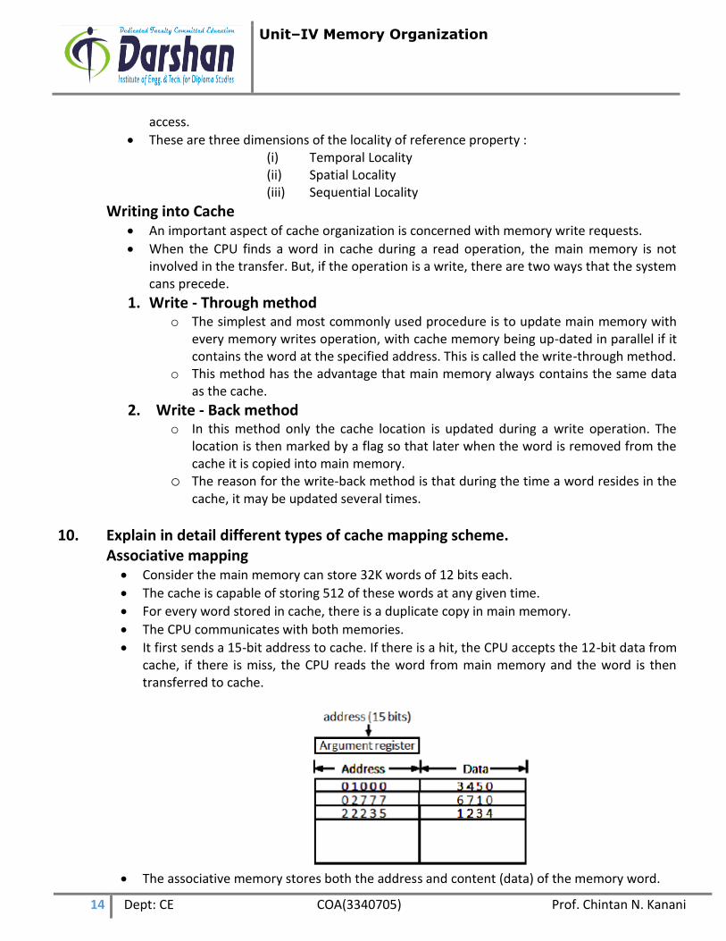
Consider the main memory can store 32K words of 12 bits each.
The cache is capable of storing 512 of these words at any given time.
For every word stored in cache, there is a duplicate copy in main memory.
The CPU communicates with both memories.
It first sends a 15-bit address to cache. If there is a hit, the CPU accepts the 12-bit data from cache, if there is miss, the CPU reads the word from main memory and the word is then transferred to cache.
The associative memory stores both the address and content (data) of the memory word.
Unit–IV Memory Organization
15 Dept: CE COA(3340705) Prof. Chintan N. Kanani
This permits any location in cache to store any word from main memory.
The figure shows three words presently stored in the cache. The address value of 15 bits is shown as a five-digit octal number and its corresponding 12-bit word is shown as a four-digit octal number.
A CPU address of 15 bits is placed in the argument register and the associative memory is searched for a matching address.
If the address is found the corresponding 12-bit data is read and sent to CPU.
If no match occurs, the main memory is accessed for the word.
The address data pairs then transferred to the associative cache memory.
If the cache is full, an address data pair must be displaced to make room for a pair that is needed and not presently in the cache.
This constitutes a first-in first-one (FIFO) replacement policy.
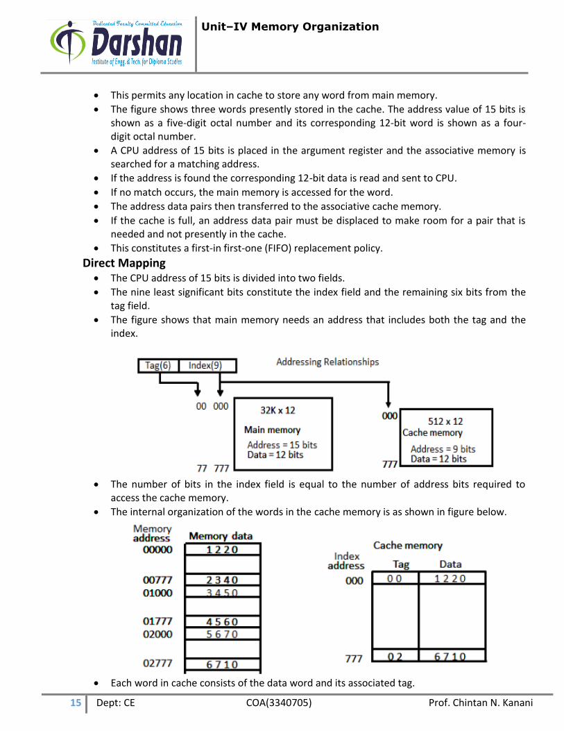
Direct Mapping The CPU address of 15 bits is divided into two fields.
The nine least significant bits constitute the index field and the remaining six bits from the tag field.
The figure shows that main memory needs an address that includes both the tag and the index.
The number of bits in the index field is equal to the number of address bits required to
access the cache memory.
The internal organization of the words in the cache memory is as shown in figure below.
Each word in cache consists of the data word and its associated tag.

Unit–IV Memory Organization
16 Dept: CE COA(3340705) Prof. Chintan N. Kanani
When a new word is first brought into the cache, the tag bits are stored alongside the data bits.
When the CPU generates a memory request the index field is used for the address to access the cache.
The tag field of the CPU address is compared with the tag in the word read from the cache.
If the two tags match, there is a hit and the desired data word is in cache.
If there is no match, there is a miss and the required word is read from main memory.
It is then stored in the cache together with the new tag, replacing the previous value.
The word at address zero is presently stored in the cache (index = 000, tag = 00, data = 1220).
Suppose that the CPU now wants to access the word at address 02000.
The index address is 000, so it is used to access the cache. The two tags are then compared.
The cache tag is 00 but the address tag is 02, which does not produce a match.
Therefore, the main memory is accessed and the data word 5670 is transferred to the CPU.
The cache word at index address 000 is then replaced with a tag of 02 and data of 5670.
The disadvantage of direct mapping is that two words with the same index in their address but with different tag values cannot reside in cache memory at the same time.
Set-associative mapping A third type of cache organization, called set associative mapping in that each word of cache
can store two or more words of memory under the same index address.
Each data word is stored together with its tag and the number of tag-data items in one word of cache is said to form a set.
An example one set-associative cache organization for a set size of two is shown in figure below.
Each index address refers to two data words and their associated terms.
Each tag required six bits and each data word has 12 bits, so the word length is 2 (6+12) = 36 bits.
An index address of nine bits can accommodate 512 words.
Thus the size of cache memory is 512 × 36. It can accommodate 1024 words or main memory since each word of cache contains two data words.
In generation a set-associative cache of set size k will accommodate K word of main memory in each word of cache.
The octal numbers listed in figure 9.8 are with reference to the main memory contents.

Unit–IV Memory Organization
17 Dept: CE COA(3340705) Prof. Chintan N. Kanani
The words stored at addresses 01000 and 02000 of main memory are stored in cache memory at index address 000.
Similarly, the words at addresses 02777 and 00777 are stored in cache at index address 777.
When the CPU generates a memory request, the index value of the address is used to access the cache.
The tag field of the CPU address is then compared with both tags in the cache to determine if a match occurs.
The comparison logic is done by an associative search of the tags in the set similar to an associative memory search: thus the name "set-associative”.
When a miss occurs in a set-associative cache and the set is full, it is necessary to replace one of the tag-data items with a new value.
The most common replacement algorithms used are: random replacement, first-in first-out (FIFO), and least recently used (LRU).
11. Explain in detail virtual memory.[Winter-2015, Summer-2014] Virtual Memory
Virtual memory is used to give programmers the illusion that they have a very large memory at their disposal, even though the computer actually has a relatively small main memory.
A virtual memory system provides a mechanism for translating program-generated addresses into correct main memory locations.
Address space An address used by a programmer will be called a virtual address, and the set of such
addresses is known as address space.
Memory space An address in main memory is called a location or physical address. The set of such locations
is called the memory space.
As an illustration, consider a computer with a main-memory capacity of 32K words (K
=1024). Fifteen bits are needed to specify a physical address in memory since 32K = 215.

Unit–IV Memory Organization
18 Dept: CE COA(3340705) Prof. Chintan N. Kanani
Suppose that the computer has available auxiliary memory for storing 220 = 1024K words.
Thus auxiliary memory has a capacity for storing information equivalent to the capacity of 32 main memories.
Denoting the address space by N and the memory space by M, we then have for this example N = 1024K and M = 32K.
In a multiprogramming computer system, programs and data are transferred to and from auxiliary memory and main memory based on demands imposed by the CPU.
Suppose that program 1 is currently being executed in the CPU. Program 1 and a portion of its associated data are moved from auxiliary memory into main memory as shown in figure.
Portions of programs and data need not be in contiguous locations in memory since information is being moved in and out, and empty spaces may be available in scattered locations in memory.
In our example, the address field of an instruction code will consist of 20 bits but physical memory addresses must be specified with only 15 bits.
Thus CPU will reference instructions and data with a 20-bit address, but the information at this address must be taken from physical memory because access to auxiliary storage for individual words will be too long.
11. Explain daisy chain priority interrupt system.[winter-2016] Determines which interrupt is to be served first when two or more requests are made
simultaneously
Also determines which interrupts are permitted to interrupt the computer while another is being serviced
Higher priority interrupts can make requests while servicing a lower priority interrupt. Daisy Chaining Priority
The daisy-chaining method of establishing priority consists of a serial connection of all
devices that request an interrupt.
The device with the highest priority is placed in the first position, followed by lower priority devices up to the device with the lowest priority, which is placed last in the chain.
This method of connection between three devices and the CPU is shown in figure
If any device has its interrupt signal in the low-level state, the interrupt line goes to the low-level state and enables the interrupt input in the CPU.
When no interrupts are pending, the interrupt line stays in the high-level state and no interrupts are recognized by the CPU.
Unit–IV Memory Organization
19 Dept: CE COA(3340705) Prof. Chintan N. Kanani
The CPU responds to an interrupt request by enabling the interrupt acknowledge line.
This signal passes on to the next device through the PO (priority out) output only if device 1 is not requesting an interrupt.
If device 1 has a pending interrupt, it blocks the acknowledge signal from the next device by placing a 0 in the PO output.
It then proceeds to insert its own interrupt vector address (VAD) into the data bus for the CPU to use during the interrupt cycle.
A device with a 0 in its Pl input generates a 0 in its PO output to inform the next-lower priority device that the acknowledge signal has been blocked.
A device that is requesting an interrupt and has a 1 in its Pl input will intercept the acknowledge signal by placing a 0 in its PO output.
If the device does not have pending interrupts, it transmits the acknowledge signal to the next device by placing a 1 in its PO output.
Thus the device with Pl = 1 and PO = 0 is the one with the highest priority that is requesting an interrupt, and this device places its VAD on the data bus.
The daisy chain arrangement gives the highest priority to the device that receives the interrupt acknowledge signal from the CPU.
The farther the device is from the first position; the lower is its priority.


