1 Data-Converter Circuits. Copyright 2004 by Oxford University Press, Inc. Microelectronic Circuits...
18
1 ata-Converter Circuits
-
date post
19-Dec-2015 -
Category
Documents
-
view
233 -
download
4
Transcript of 1 Data-Converter Circuits. Copyright 2004 by Oxford University Press, Inc. Microelectronic Circuits...

1
Data-Converter Circuits

Microelectronic Circuits - Fifth Edition Sedra/Smith 2Copyright 2004 by Oxford University Press, Inc.
Figure 9.31 Cascading the small-signal equivalent circuits of the individual stages for the evaluation of the overall voltage gain.

Microelectronic Circuits - Fifth Edition Sedra/Smith 3Copyright 2004 by Oxford University Press, Inc.
Figure 9.32 Bode plot for the 741 gain, neglecting nondominant poles.

Microelectronic Circuits - Fifth Edition Sedra/Smith 4Copyright 2004 by Oxford University Press, Inc.
Figure 9.33 A simple model for the 741 based on modeling the second stage as an integrator.

Microelectronic Circuits - Fifth Edition Sedra/Smith 5Copyright 2004 by Oxford University Press, Inc.
Figure 9.34 A unity-gain follower with a large step input. Since the output voltage cannot change instantaneously, a large differential voltage appears between the op-amp input terminals.

Microelectronic Circuits - Fifth Edition Sedra/Smith 6Copyright 2004 by Oxford University Press, Inc.
Figure 9.35 Model for the 741 op amp when a large positive differential signal is applied.
Microelectronic Circuits - Fifth Edition Sedra/Smith 7Copyright 2004 by Oxford University Press, Inc.
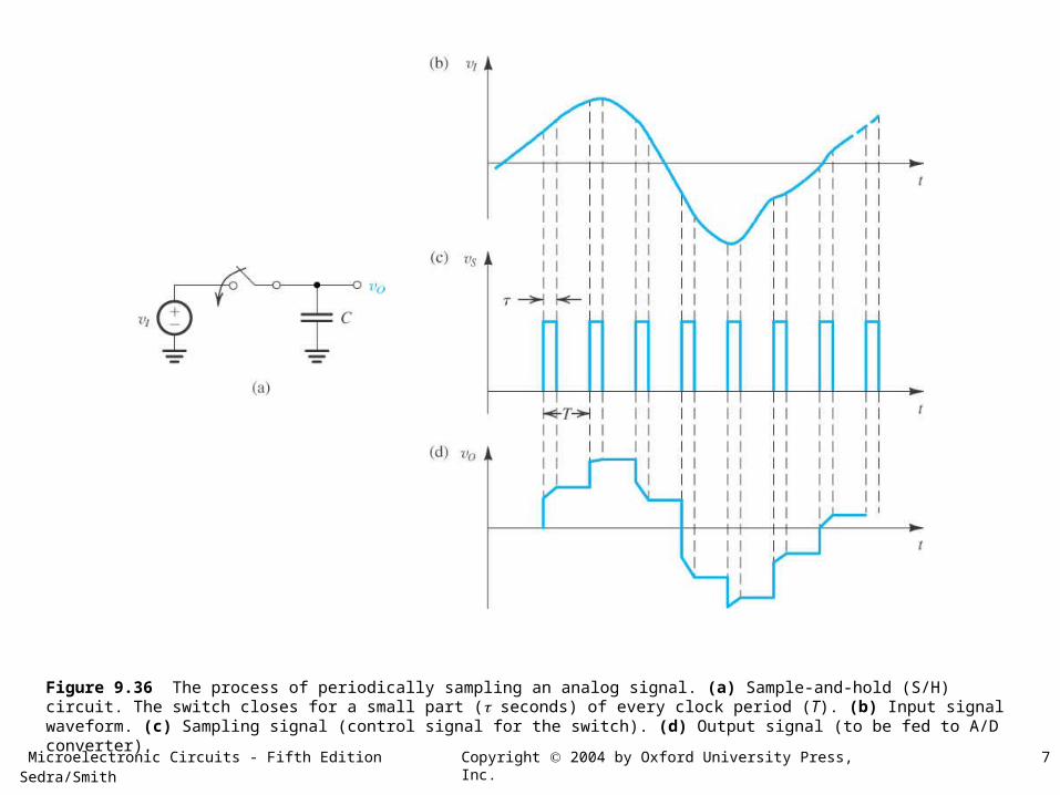
Figure 9.36 The process of periodically sampling an analog signal. (a) Sample-and-hold (S/H) circuit. The switch closes for a small part ( seconds) of every clock period (T). (b) Input signal waveform. (c) Sampling signal (control signal for the switch). (d) Output signal (to be fed to A/D converter).

Microelectronic Circuits - Fifth Edition Sedra/Smith 8Copyright 2004 by Oxford University Press, Inc.
Figure 9.37 The A/D and D/A converters as circuit blocks.

Microelectronic Circuits - Fifth Edition Sedra/Smith 9Copyright 2004 by Oxford University Press, Inc.
Figure 9.38 The analog samples at the output of a D/A converter are usually fed to a sample-and-hold circuit to obtain the staircase waveform shown. This waveform can then be filtered to obtain the smooth waveform, shown in color. The time delay usually introduced by the filter is not shown.

Microelectronic Circuits - Fifth Edition Sedra/Smith 10Copyright 2004 by Oxford University Press, Inc.
Figure 9.39 An N-bit D/A converter using a binary-weighted resistive ladder network.

Microelectronic Circuits - Fifth Edition Sedra/Smith 11Copyright 2004 by Oxford University Press, Inc.
Figure 9.40 The basic circuit configuration of a DAC utilizing an R-2R ladder network.

Microelectronic Circuits - Fifth Edition Sedra/Smith 12Copyright 2004 by Oxford University Press, Inc.
Figure 9.41 A practical circuit implementation of a DAC utilizing an R-2R ladder network.
Microelectronic Circuits - Fifth Edition Sedra/Smith 13Copyright 2004 by Oxford University Press, Inc.
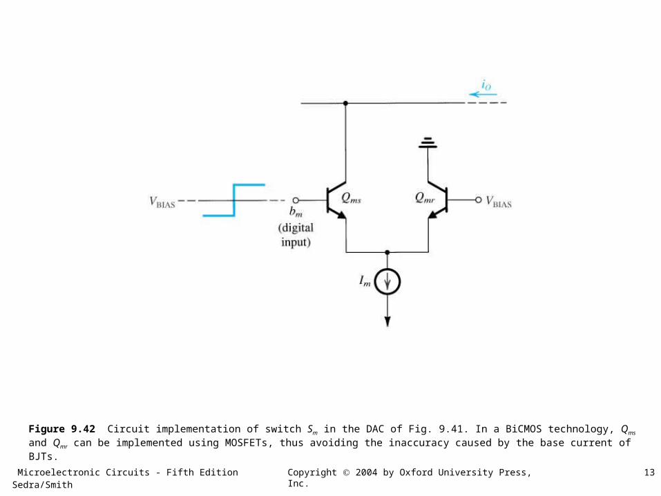
Figure 9.42 Circuit implementation of switch Sm in the DAC of Fig. 9.41. In a BiCMOS technology, Qms and Qmr can be implemented using MOSFETs, thus avoiding the inaccuracy caused by the base current of BJTs.

Microelectronic Circuits - Fifth Edition Sedra/Smith 14Copyright 2004 by Oxford University Press, Inc.
Figure 9.43 A simple feedback-type A/D converter.

Microelectronic Circuits - Fifth Edition Sedra/Smith 15Copyright 2004 by Oxford University Press, Inc.
Figure 9.44 The dual-slope A/D conversion method. Note that vA is assumed to be negative.

Microelectronic Circuits - Fifth Edition Sedra/Smith 16Copyright 2004 by Oxford University Press, Inc.
Figure 9.44 (Continued)
Microelectronic Circuits - Fifth Edition Sedra/Smith 17Copyright 2004 by Oxford University Press, Inc.
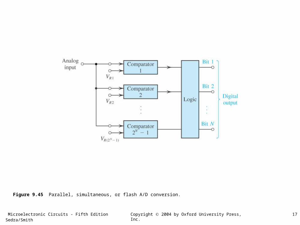
Figure 9.45 Parallel, simultaneous, or flash A/D conversion.

Microelectronic Circuits - Fifth Edition Sedra/Smith 18Copyright 2004 by Oxford University Press, Inc.
Figure 9.46 Charge-redistribution A/D converter suitable for CMOS implementation: (a) sample phase, (b) hold phase, and (c) charge-redistribution phase.