1 A/0.6 A, DC-to-DC Switching Regulator with Independent ... · PDF file1 A/0.6 A, DC-to-DC...
27
1 A/0.6 A, DC-to-DC Switching Regulator with Independent Positive and Negative Outputs Data Sheet ADP5070 Rev. B Document Feedback Information furnished by Analog Devices is believed to be accurate and reliable. However, no responsibility is assumed by Analog Devices for its use, nor for any infringements of patents or other rights of third parties that may result from its use. Specifications subject to change without notice. No license is granted by implication or otherwise under any patent or patent rights of Analog Devices. Trademarks and registered trademarks are the property of their respective owners. One Technology Way, P.O. Box 9106, Norwood, MA 02062-9106, U.S.A. Tel: 781.329.4700 ©2015–2017 Analog Devices, Inc. All rights reserved. Technical Support www.analog.com FEATURES Wide input supply voltage range: 2.85 V to 15 V Generates well regulated, independently resistor programmable VPOS and VNEG outputs Boost regulator to generate VPOS output Adjustable positive output to 39 V Integrated 1.0 A main switch Optional single-ended primary-inductor converter (SEPIC) configuration for automatic step-up/step-down Inverting regulator to generate VNEG output Adjustable negative output to VIN − 39 V Integrated 0.6 A main switch True shutdown for both positive and negative outputs 1.2 MHz/2.4 MHz switching frequency with optional external frequency synchronization from 1.0 MHz to 2.6 MHz Resistor programmable soft start timer Slew rate control for lower system noise Individual precision enable and flexible start-up sequence control for symmetric start, VPOS first, or VNEG first Out-of-phase operation UVLO, OCP, OVP, and TSD protection 4 mm × 4 mm, 20-lead LFCSP and 20-lead TSSOP −40°C to +125°C junction temperature range Supported by the ADIsimPower tool set APPLICATIONS Bipolar amplifiers, ADCs, DACs and multiplexers Charge-coupled device (CCD) bias supply Optical module supply RF power amplifier (PA) bias TYPICAL APPLICATION CIRCUIT ADP5070 SS INBK SW1 R C1 C C1 COMP1 R C2 C C2 COMP2 C VREG VREG EN1 SYNC/FREQ SLEW SEQ EN2 AGND PVIN1 PVIN2 PVINSYS C IN1 V IN FB1 D1 L1 L2 R FB1 R FT1 V POS SW2 PGND FB2 VREF D2 R FB2 R FT2 V NEG C VREF C OUT1 C OUT2 12068-001 Figure 1. GENERAL DESCRIPTION The ADP5070 is a dual high performance dc-to-dc regulator that generates independently regulated positive and negative rails. The input voltage range of 2.85 V to 15 V supports a wide variety of applications. The integrated main switch in both regulators enables generation of an adjustable positive output voltage up to +39 V and a negative output voltage down to −39 V below input voltage. The ADP5070 operates at a pin selected 1.2 MHz/2.4 MHz switching frequency. The ADP5070 can synchronize with an external oscillator from 1.0 MHz to 2.6 MHz to ease noise filtering in sensitive applications. Both regulators implement programmable slew rate control circuitry for the MOSFET driver stage to reduce electromagnetic interference (EMI). Flexible start-up sequencing is provided with the options of manual enable, simultaneous mode, positive supply first, and negative supply first. The ADP5070 includes a fixed internal or resistor programmable soft start timer to prevent inrush current at power-up. During shutdown, both regulators completely disconnect the loads from the input supply to provide a true shutdown. Other key safety features in the ADP5070 include overcurrent protection (OCP), overvoltage protection (OVP), thermal shutdown (TSD), and input undervoltage lockout (UVLO). The ADP5070 is available in a 20-lead LFCSP or in a 20-lead TSSOP and is rated for a −40°C to +125°C junction temperature range. Table 1. Family Models Model Boost Switch (A) Inverter Switch (A) ADP5070 1.0 0.6 ADP5071 2.0 1.2
Transcript of 1 A/0.6 A, DC-to-DC Switching Regulator with Independent ... · PDF file1 A/0.6 A, DC-to-DC...

1 A/0.6 A, DC-to-DC Switching Regulator with Independent Positive and Negative Outputs
Data Sheet ADP5070
Rev. B Document Feedback Information furnished by Analog Devices is believed to be accurate and reliable. However, no responsibility is assumed by Analog Devices for its use, nor for any infringements of patents or other rights of third parties that may result from its use. Specifications subject to change without notice. No license is granted by implication or otherwise under any patent or patent rights of Analog Devices. Trademarks and registered trademarks are the property of their respective owners.
One Technology Way, P.O. Box 9106, Norwood, MA 02062-9106, U.S.A. Tel: 781.329.4700 ©2015–2017 Analog Devices, Inc. All rights reserved. Technical Support www.analog.com
FEATURES Wide input supply voltage range: 2.85 V to 15 V Generates well regulated, independently resistor
programmable VPOS and VNEG outputs Boost regulator to generate VPOS output
Adjustable positive output to 39 V Integrated 1.0 A main switch Optional single-ended primary-inductor converter (SEPIC)
configuration for automatic step-up/step-down Inverting regulator to generate VNEG output
Adjustable negative output to VIN − 39 V Integrated 0.6 A main switch
True shutdown for both positive and negative outputs 1.2 MHz/2.4 MHz switching frequency with optional external
frequency synchronization from 1.0 MHz to 2.6 MHz Resistor programmable soft start timer Slew rate control for lower system noise Individual precision enable and flexible start-up sequence
control for symmetric start, VPOS first, or VNEG first Out-of-phase operation UVLO, OCP, OVP, and TSD protection 4 mm × 4 mm, 20-lead LFCSP and 20-lead TSSOP −40°C to +125°C junction temperature range Supported by the ADIsimPower tool set
APPLICATIONS Bipolar amplifiers, ADCs, DACs and multiplexers Charge-coupled device (CCD) bias supply Optical module supply RF power amplifier (PA) bias
TYPICAL APPLICATION CIRCUIT
ADP5070SS INBK
SW1
RC1
CC1COMP1
RC2
CC2COMP2
CVREGVREG
EN1
SYNC/FREQSLEWSEQ
EN2
AGND
PVIN1PVIN2PVINSYSCIN1
VIN
FB1
D1
L1
L2
RFB1
RFT1
VPOS
SW2
PGND
FB2
VREF
D2
RFB2
RFT2
VNEG
CVREF
COUT1
COUT2
1206
8-00
1
Figure 1.
GENERAL DESCRIPTION The ADP5070 is a dual high performance dc-to-dc regulator that generates independently regulated positive and negative rails.
The input voltage range of 2.85 V to 15 V supports a wide variety of applications. The integrated main switch in both regulators enables generation of an adjustable positive output voltage up to +39 V and a negative output voltage down to −39 V below input voltage.
The ADP5070 operates at a pin selected 1.2 MHz/2.4 MHz switching frequency. The ADP5070 can synchronize with an external oscillator from 1.0 MHz to 2.6 MHz to ease noise filtering in sensitive applications. Both regulators implement programmable slew rate control circuitry for the MOSFET driver stage to reduce electromagnetic interference (EMI).
Flexible start-up sequencing is provided with the options of manual enable, simultaneous mode, positive supply first, and negative supply first.
The ADP5070 includes a fixed internal or resistor programmable soft start timer to prevent inrush current at power-up. During shutdown, both regulators completely disconnect the loads from the input supply to provide a true shutdown.
Other key safety features in the ADP5070 include overcurrent protection (OCP), overvoltage protection (OVP), thermal shutdown (TSD), and input undervoltage lockout (UVLO).
The ADP5070 is available in a 20-lead LFCSP or in a 20-lead TSSOP and is rated for a −40°C to +125°C junction temperature range.
Table 1. Family Models Model Boost Switch (A) Inverter Switch (A) ADP5070 1.0 0.6 ADP5071 2.0 1.2
ADP5070 Data Sheet
Rev. B | Page 2 of 27
TABLE OF CONTENTS Features .............................................................................................. 1
Applications ....................................................................................... 1
Typical Application Circuit ............................................................. 1
General Description ......................................................................... 1
Revision History ............................................................................... 2
Specifications ..................................................................................... 3
Absolute Maximum Ratings ............................................................ 5
Thermal Resistance ...................................................................... 5
ESD Caution .................................................................................. 5
Pin Configurations and Function Descriptions ........................... 6
Typical Performance Characteristics ............................................. 8
Theory of Operation ...................................................................... 14
PWM Mode ................................................................................. 14
PSM Mode ................................................................................... 14
Undervoltage Lockout (UVLO) ............................................... 14
Oscillator and Synchronization ................................................ 14
Internal Regulators ..................................................................... 14
Precision Enabling ...................................................................... 15
Soft Start ...................................................................................... 15
Slew Rate Control ....................................................................... 15
Current-Limit Protection ............................................................ 15
Overvoltage Protection .............................................................. 15
Thermal Shutdown .................................................................... 15
Start-Up Sequence ...................................................................... 15
Applications Information .............................................................. 17
ADIsimPower Design Tool ....................................................... 17
Component Selection ................................................................ 17
Loop Compensation .................................................................. 20
Common Applications .............................................................. 22
Super Low Noise With Optional LDOs................................... 24
SEPIC Step-Up/Step-Down Operation ................................... 25
Layout Considerations ............................................................... 26
Outline Dimensions ....................................................................... 27
Ordering Guide .......................................................................... 27
REVISION HISTORY 7/2017—Rev. A to Rev. B Changes to Table 10 and Table 11 ................................................ 23 Updated Outline Dimensions ....................................................... 27 Changes to Ordering Guide .......................................................... 27 6/2015—Rev. 0 to Rev. A Added 20-Lead TSSOP ...................................................... Universal Changes to Table 3 and Table 4 ....................................................... 5 Added Figure 3, Renumbered Sequentially .................................. 6 Changes to Figure 29 Caption and Figure 32 Caption .............. 11 Changes to Figure 37 Caption to Figure 39 Caption ................. 13 Changes to Internal Regulators Section ...................................... 14 Change to Soft Start Section.......................................................... 15 Changes to Output Capacitors Section, Soft Start Resistor Section, and Diodes Section ......................................................................... 18 Changes to Figure 50 Caption ....................................................... 26 Added Figure 51 .............................................................................. 26 Updated Outline Dimensions ....................................................... 27 Changes to Ordering Guide .......................................................... 27 2/2015—Revision 0: Initial Version

Data Sheet ADP5070
Rev. B | Page 3 of 27
SPECIFICATIONS PVIN1 = PVIN2 = PVINSYS = 2.85 V to 15 V, VPOS = 15 V, VNEG = −15 V, fSW = 1200 kHz, TJ = −40°C to +125°C for minimum/maximum specifications, and TA = 25°C for typical specifications, unless otherwise noted.
Table 2. Parameter Symbol Min Typ Max Unit Test Conditions/Comments INPUT SUPPLY VOLTAGE RANGE VIN 2.85 15 V PVIN1, PVIN2, PVINSYS QUIESCENT CURRENT
Operating Quiescent Current PVIN1, PVIN2, PVINSYS (Total) IQ 3.5 4.0 mA No switching, EN1 = EN2 = high,
PVIN1 = PVIN2 = PVINSYS = 5 V Shutdown Current ISHDN 5 10 µA No switching, EN1 = EN2 = low, PVIN1 =
PVIN2 = PVINSYS = 5 V UVLO
System UVLO Threshold PVINSYS Rising VUVLO_RISING 2.8 2.85 V Falling VUVLO_FALLING 2.5 2.55 V Hysteresis VHYS_1 0.25 V
OSCILLATOR CIRCUIT Switching Frequency fSW 1.130 1.200 1.270 MHz SYNC/FREQ = low 2.240 2.400 2.560 MHz SYNC/FREQ = high (connect to VREG) SYNC/FREQ Input
Input Clock Range fSYNC 1.000 2.600 MHz Input Clock Minimum On Pulse Width tSYNC_MIN_ON 100 ns Input Clock Minimum Off Pulse Width tSYNC_MIN_OFF 100 ns Input Clock High Logic VH (SYNC) 1.3 V Input Clock Low Logic VL (SYNC) 0.4 V
PRECISION ENABLING (EN1, EN2) High Level Threshold VTH_H 1.125 1.15 1.175 V Low Level Threshold VTH_L 1.025 1.05 1.075 V Shutdown Mode VTH_S 0.4 V Internal circuitry disabled to achieve
ISHDN Pull-Down Resistance REN 1.48 MΩ
INTERNAL REGULATOR VREG Output Voltage VREG 4.25 V
BOOST REGULATOR Feedback Voltage VFB1 0.8 V Feedback Voltage Accuracy −0.5 +0.5 % TJ = 25°C −1.5 +1.5 % TJ = −40°C to +125°C Feedback Bias Current IFB1 0.1 µA Overvoltage Protection Threshold VOV1 0.86 V At FB1 pin Load Regulation ∆VFB1/ILOAD1 0.0003 %/mA ILOAD1
1 = 5 mA to 150 mA Line Regulation ∆VFB1/VPVIN1 0.002 %/V VPVIN1 = 2.85 V to 14.5 V, ILOAD1
1 = 15 mA Error Amplifier (EA) Transconductance gM1 270 300 330 µA/V Power FET On Resistance RDS (ON) BOOST 175 mΩ Power FET Maximum Drain Source
Voltage VDS (MAX) BOOST 39 V
Input Disconnect Switch On Resistance RDS (ON) INBK 210 mΩ Current-Limit Threshold ILIM (BOOST) 1.00 1.10 1.20 A Minimum On Time 50 ns Minimum Off Time 25 ns

ADP5070 Data Sheet
Rev. B | Page 4 of 27
Parameter Symbol Min Typ Max Unit Test Conditions/Comments INVERTING REGULATOR
Reference Voltage VREF 1.60 V Reference Voltage Accuracy −0.5 +0.5 % TJ = 25°C −1.5 +1.5 % TJ = −40°C to +125°C Feedback Voltage VREF − VFB2 0.8 V Feedback Voltage Accuracy −0.5 +0.5 % TJ = 25°C −1.5 +1.5 % TJ = −40°C to +125°C Feedback Bias Current IFB2 0.1 µA Overvoltage Protection Threshold VOV2 0.74 V At FB2 pin after soft start has completed Load Regulation ∆(VREF − VFB2)/
ILOAD2 0.0004 %/mA ILOAD2
1 = 5 mA to 75 mA
Line Regulation ∆(VREF − VFB2)/ VPVIN2
0.003 %/V VPVIN2 = 2.85 V to 14.5 V, ILOAD21 = 15 mA
EA Transconductance gM2 270 300 330 µA/V Power FET On Resistance RDS (ON) INVERTER 350 mΩ Power FET Maximum Drain Source
Voltage VDS (MAX) INVERTER 39 V
Current-Limit Threshold ILIM (INVERTER) 600 660 720 mA Minimum On Time 60 ns Minimum Off Time 50 ns
SOFT START Soft Start Timer for Boost and Inverting
Regulators tSS 4 ms SS = open
32 ms SS resistor = 50 kΩ to GND Hiccup Time tHICCUP 8 × tSS ms
THERMAL SHUTDOWN Threshold TSHDN 150 °C Hysteresis THYS 15 °C
1 ILOADx is the current through a resistive load connected across the output capacitor (where x is 1 for the boost regulator load and 2 for the inverting regulator load).

Data Sheet ADP5070
Rev. B | Page 5 of 27
ABSOLUTE MAXIMUM RATINGS Table 3. Parameter Rating PVIN1, PVIN2, PVINSYS −0.3 V to +18 V INBK −0.3 V to PVIN1 + 0.3 V SW1 −0.3 V to +40 V SW2 PVIN2 − 40 V to PVIN2 + 0.3 V PGND, AGND −0.3 V to +0.3 V VREG −0.3 V to lower of PVINSYS +
0.3 V or +6 V EN1, EN2, FB1, FB2, SYNC/FREQ −0.3 V to +6 V COMP1, COMP2, SLEW, SS,
SEQ, VREF −0.3 V to VREG + 0.3 V
Operating Junction Temperature Range
−40°C to +125°C
Storage Temperature Range −65°C to +150°C Soldering Conditions JEDEC J-STD-020
Stresses at or above those listed under Absolute Maximum Ratings may cause permanent damage to the product. This is a stress rating only; functional operation of the product at these or any other conditions above those indicated in the operational section of this specification is not implied. Operation beyond the maximum operating conditions for extended periods may affect product reliability.
THERMAL RESISTANCE θJA and ΨJT are based on a 4-layer printed circuit board (PCB) (two signal and two power planes) with nine thermal vias connecting the exposed pad to the ground plane as recommended in the Layout Considerations section. θJC is measured at the top of the package and is independent of the PCB. The ΨJT value is more appropriate for calculating junction to case temperature in the application.
Table 4. Thermal Resistance Package Type θJA θJC ΨJT Unit 20-Lead LFCSP 60.2 36.5 0.63 °C/W 20-Lead TSSOP 58.5 35.0 0.60 °C/W
ESD CAUTION

ADP5070 Data Sheet
Rev. B | Page 6 of 27
PIN CONFIGURATIONS AND FUNCTION DESCRIPTIONS
141312
1
34
VREG15 PVIN1
AGNDVREF
11 FB2
INBK
SEQ2SYNC/FREQ
SLEW5FB1
7EN
16
CO
MP1
8SS
9EN
210
CO
MP2
19PG
ND
20SW
1
18SW
217
PVIN
216
PVIN
SYS
ADP5070TOP VIEW
(Not to Scale)
NOTES1. EXPOSED PAD. CONNECT THE EXPOSED PAD TO AGND. 12
068-
002
Figure 2. 20-Lead LFCSP Pin Configuration
1
2
3
4
5
6
7
8
9
10
20
19
18
17
16
15
14
13
12
11
SW1
INBK
SYNC/FREQ
FB1
SLEW
SEQ
PGND
PVIN2
PVINSYS
PVIN1
VREF
AGND
VREG
SS
EN1
COMP1
EN2
COMP2
FB2
SW2
ADP5070TOP VIEW
1206
8-05
0
NOTES1. EXPOSED PAD. CONNECT THE EXPOSED PAD TO AGND.
Figure 3. 20-Lead TSSOP Pin Configuration
Table 5. Pin Function Descriptions Pin No.
Mnemonic Description LFCSP TSSOP 1 3 INBK Input Disconnect Switch Output for the Boost Regulator. 2 4 SYNC/FREQ Frequency Setting and Synchronization Input. To set the switching frequency to 2.4 MHz, pull the SYNC/FREQ
pin high. To set the switching frequency to 1.2 MHz, pull the SYNC/FREQ pin low. To synchronize the switching frequency, connect the SYNC/FREQ pin to an external clock.
3 5 SEQ Start-Up Sequence Control. For manual VPOS/VNEG startup using an individual precision enabling pin, leave the SEQ pin open. For simultaneous VPOS/VNEG startup when the EN2 pin rises, connect the SEQ pin to VREG (the EN1 pin can be used to enable the internal references early, if required). For a sequenced startup, pull the SEQ pin low. Either EN1 or EN2 can be used, and the corresponding supply is the first in sequence; hold the other enable pin low.
4 6 SLEW Driver Stage Slew Rate Control. The SLEW pin sets the slew rate for the SW1 and SW2 drivers. For the fastest slew rate (best efficiency), leave the SLEW pin open. For normal slew rate, connect the SLEW pin to VREG. For the slowest slew rate (best noise performance), connect the SLEW pin to AGND.
5 7 FB1 Feedback Input for the Boost Regulator. Connect a resistor divider between the positive side of the boost regulator output capacitor and AGND to program the output voltage.
6 8 COMP1 Error Amplifier Compensation for the Boost Regulator. Connect the compensation network between this pin and AGND.
7 9 EN1 Boost Regulator Precision Enable. The EN1 pin is compared to an internal precision reference to enable the boost regulator output.
8 10 SS Soft Start Programming. Leave the SS pin open to obtain the fastest soft start time. To program a slower soft start time, connect a resistor between the SS pin and AGND.
9 11 EN2 Inverting Regulator Precision Enable. The EN2 pin is compared to an internal precision reference to enable the inverting regulator output.
10 12 COMP2 Error Amplifier Compensation for the Inverting Regulator. Connect the compensation network between this pin and AGND.
11 13 FB2 Feedback Input for the Inverting Regulator. Connect a resistor divider between the negative side of the inverting regulator output capacitor and VREF to program the output voltage.
12 14 VREF Inverting Regulator Reference Output. Connect a 1.0 µF ceramic filter capacitor between the VREF pin and AGND.
13 15 AGND Analog Ground. 14 16 VREG Internal Regulator Output. Connect a 1.0 µF ceramic filter capacitor between the VREG pin and AGND. 15 17 PVIN1 Power Input for the Boost Regulator. 16 18 PVINSYS System Power Supply for the ADP5070. 17 19 PVIN2 Power Input for the Inverting Regulator.

Data Sheet ADP5070
Rev. B | Page 7 of 27
Pin No.
Mnemonic Description LFCSP TSSOP 18 20 SW2 Switching Node for the Inverting Regulator. 19 1 PGND Power Ground for the Boost and Inverting Regulators. 20 2 SW1 Switching Node for the Boost Regulator. EPAD Exposed Pad. Connect the exposed pad to AGND.
ADP5070 Data Sheet
Rev. B | Page 8 of 27
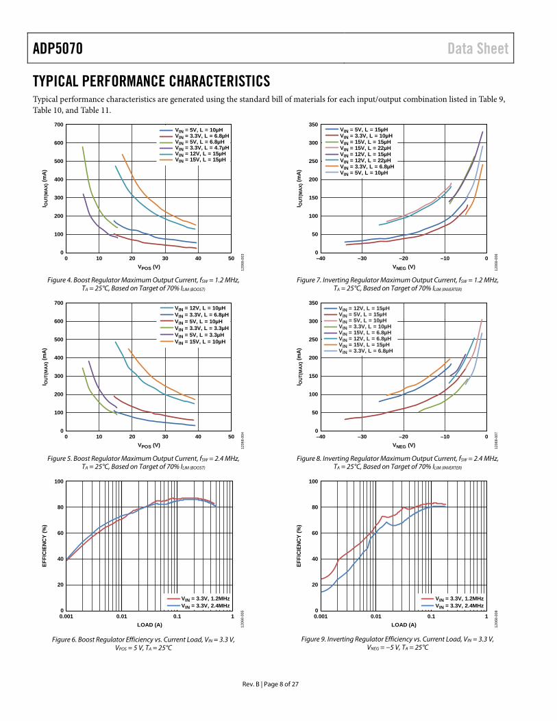
TYPICAL PERFORMANCE CHARACTERISTICS Typical performance characteristics are generated using the standard bill of materials for each input/output combination listed in Table 9, Table 10, and Table 11.
700
0
100
200
300
400
500
600
0 10 20 30 40 50
I OUT
(MAX
) (m
A)
VPOS (V)
VIN = 5V, L = 10µHVIN = 3.3V, L = 6.8µHVIN = 5V, L = 6.8µHVIN = 3.3V, L = 4.7µHVIN = 12V, L = 15µHVIN = 15V, L = 15µH
1206
8-00
3
Figure 4. Boost Regulator Maximum Output Current, fSW = 1.2 MHz,
TA = 25°C, Based on Target of 70% ILIM (BOOST)
700
0
100
200
300
400
500
600
0 10 20 30 40 50
I OUT
(MAX
) (m
A)
VPOS (V)
VIN = 12V, L = 10µHVIN = 3.3V, L = 6.8µHVIN = 5V, L = 10µHVIN = 3.3V, L = 3.3µHVIN = 5V, L = 3.3µHVIN = 15V, L = 10µH
1206
8-00
4
Figure 5. Boost Regulator Maximum Output Current, fSW = 2.4 MHz,
TA = 25°C, Based on Target of 70% ILIM (BOOST)
100
0
20
40
60
80
0.001 0.01 0.1 1
EFFI
CIEN
CY (%
)
LOAD (A)
VIN = 3.3V, 1.2MHzVIN = 3.3V, 2.4MHz
1206
8-00
5
Figure 6. Boost Regulator Efficiency vs. Current Load, VIN = 3.3 V, VPOS = 5 V, TA = 25°C
350
0
50
100
150
200
250
300
–40 –30 –20 –10 0
I OUT
(MAX
) (m
A)
VNEG (V)
VIN = 5V, L = 15µHVIN = 3.3V, L = 10µHVIN = 15V, L = 15µH
VIN = 12V, L = 15µHVIN = 12V, L = 22µH
VIN = 5V, L = 10µHVIN = 3.3V, L = 6.8µH
VIN = 15V, L = 22µH
1206
8-00
6
Figure 7. Inverting Regulator Maximum Output Current, fSW = 1.2 MHz,
TA = 25°C, Based on Target of 70% ILIM (INVERTER)
350
0
50
100
150
200
250
300
–40 –30 –20 –10 0
I OUT
(MAX
) (m
A)
VNEG (V)
VIN = 12V, L = 15µHVIN = 5V, L = 15µHVIN = 5V, L = 10µHVIN = 3.3V, L = 10µHVIN = 15V, L = 6.8µHVIN = 12V, L = 6.8µHVIN = 15V, L = 15µHVIN = 3.3V, L = 6.8µH
1206
8-00
7
Figure 8. Inverting Regulator Maximum Output Current, fSW = 2.4 MHz,
TA = 25°C, Based on Target of 70% ILIM (INVERTER)
100
0
20
40
60
80
0.001 0.01 0.1 1
EFFI
CIEN
CY (%
)
LOAD (A)
VIN = 3.3V, 1.2MHzVIN = 3.3V, 2.4MHz
1206
8-00
8
Figure 9. Inverting Regulator Efficiency vs. Current Load, VIN = 3.3 V, VNEG = −5 V, TA = 25°C

Data Sheet ADP5070
Rev. B | Page 9 of 27
100
0
20
40
60
80
0.001 0.01 0.1 1
EFFI
CIEN
CY (%
)
LOAD (A)
VIN = 3.3V, 1.2MHzVIN = 3.3V, 2.4MHzVIN = 5V, 1.2MHzVIN = 5V, 2.4MHz
1206
8-00
9
Figure 10. Boost Regulator Efficiency vs. Current Load, VPOS = 9 V,
TA = 25°C
100
0
20
40
60
80
0.001 0.01 0.1 1
EFFI
CIEN
CY (%
)
LOAD (A)
VIN = 3.3V, 1.2MHzVIN = 3.3V, 2.4MHzVIN = 5V, 1.2MHzVIN = 5V, 2.4MHz
1206
8-01
0
Figure 11. Boost Regulator Efficiency vs. Current Load, VPOS = 15 V,
TA = 25°C
100
0
20
40
60
80
0.001 0.01 0.1 1
EFFI
CIEN
CY (%
)
LOAD (A)
VIN = 5V, 1.2MHzVIN = 5V, 2.4MHz
1206
8-01
1
Figure 12. Boost Regulator Efficiency vs. Current Load, VPOS = 34 V,
TA = 25°C
100
0
20
40
60
80
0.001 0.01 0.1 1
EFFI
CIEN
CY (%
)
LOAD (A)
VIN = 3.3V, 1.2MHzVIN = 3.3V, 2.4MHzVIN = 5V, 1.2MHzVIN = 5V, 2.4MHz
1206
8-01
2
Figure 13. Inverting Regulator Efficiency vs. Current Load, VNEG = −9 V,
TA = 25°C
100
0
20
40
60
80
0.001 0.01 0.1 1
EFFI
CIEN
CY (%
)
LOAD (A)
VIN = 3.3V, 1.2MHzVIN = 3.3V, 2.4MHzVIN = 5V, 1.2MHzVIN = 5V, 2.4MHz
1206
8-01
3
Figure 14. Inverting Regulator Efficiency vs. Current Load, VNEG = −15 V,
TA = 25°C
100
0
20
40
60
80
0.001 0.01 0.1
EFFI
CIE
NC
Y (%
)
LOAD (A)
VIN = 5V, 1.2MHzVIN = 5V, 2.4MHz
1206
8-01
4
Figure 15. Inverting Regulator Efficiency vs. Current Load, VNEG = −34 V,
TA = 25°C
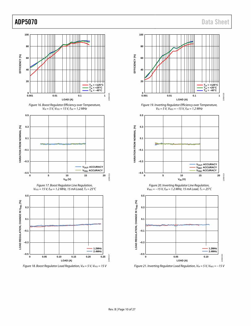
ADP5070 Data Sheet
Rev. B | Page 10 of 27
100
0
20
40
60
80
0.001 0.01 0.1 1
EFFI
CIEN
CY (%
)
LOAD (A)
TA = –40°CTA = +25°CTA = +125°C
1206
8-01
5
Figure 16. Boost Regulator Efficiency over Temperature,
VIN = 5 V, VPOS = 15 V, fSW = 1.2 MHz
0.5
–0.5
–0.3
–0.1
0.1
0.3
0 105 15 20
VARI
ATIO
N FR
OM
NO
MIN
AL (%
)
VIN (V)
VOUT ACCURACYVFB1 ACCURACY
1206
8-01
6
Figure 17. Boost Regulator Line Regulation,
VPOS = 15 V, fSW = 1.2 MHz, 15 mA Load, TA = 25°C
0.5
–0.5
–0.3
–0.1
0.1
0.3
0 0.100.05 0.15 0.250.20
LOA
D R
EGU
LATI
ON
, CH
AN
GE
IN V
FB1
(%)
LOAD (A)
1.2MHz2.4MHz
1206
8-01
7
Figure 18. Boost Regulator Load Regulation, VIN = 5 V, VPOS = 15 V
100
0
20
40
60
80
0.001 0.01 0.1 1
EFFI
CIEN
CY (%
)
LOAD (A)
TA = –40°CTA = +25°CTA = +125°C
1206
8-01
8
Figure 19. Inverting Regulator Efficiency over Temperature,
VIN = 5 V, VNEG = −15 V, fSW = 1.2 MHz
0.5
–0.5
–0.3
–0.1
0.1
0.3
0 105 15 20
VARI
ATIO
N FR
OM
NO
MIN
AL (%
)
VIN (V)
VOUT ACCURACYVREF ACCURACYVFB2 ACCURACY
1206
8-01
9
Figure 20. Inverting Regulator Line Regulation,
VNEG = −15 V, fSW = 1.2 MHz, 15 mA Load, TA = 25°C
0.5
–0.5
–0.3
–0.1
0.1
0.3
0 0.05 0.10
LOA
D R
EGU
LATI
ON
, CH
AN
GE
IN V
FB2
(%)
LOAD (A)
1.2MHz2.4MHz
1206
8-02
0
Figure 21. Inverting Regulator Load Regulation, VIN = 5 V, VNEG = −15 V
Data Sheet ADP5070
Rev. B | Page 11 of 27
0.5
–0.5
–0.3
–0.1
0.1
0.3
0 0.060.040.02 0.08 0.120.10
V FB
1 D
EVIA
TIO
N F
RO
M A
VER
AG
E VA
LUE
(%)
INVERTING REGULATOR LOAD (A) 1206
8-02
1
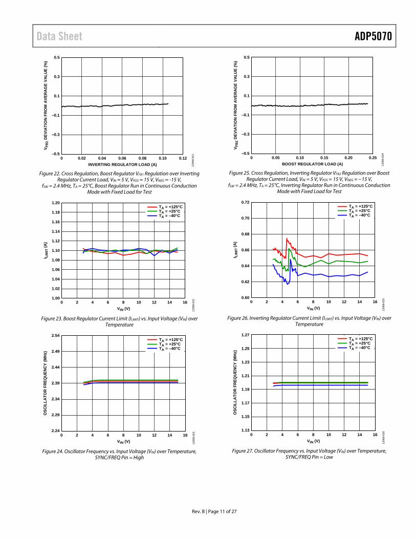
Figure 22. Cross Regulation, Boost Regulator VFB1 Regulation over Inverting
Regulator Current Load, VIN = 5 V, VPOS = 15 V, VNEG = -15 V, fSW = 2.4 MHz, TA = 25°C, Boost Regulator Run in Continuous Conduction
Mode with Fixed Load for Test
0 4 8 12 162 6 10 14
I LIM
IT (A
)
VIN (V)
TA = –40°CTA = +25°CTA = +125°C
1.00
1.02
1.04
1.06
1.08
1.10
1.12
1.14
1.16
1.18
1.20
1206
8-02
2
Figure 23. Boost Regulator Current Limit (ILIMIT) vs. Input Voltage (VIN) over
Temperature
0 4 8 12 162 6 10 14
OSC
ILLA
TOR
FREQ
UENC
Y (M
Hz)
VIN (V)
TA = –40°CTA = +25°CTA = +125°C
1206
8-02
32.24
2.29
2.34
2.39
2.44
2.49
2.54
Figure 24. Oscillator Frequency vs. Input Voltage (VIN) over Temperature,
SYNC/FREQ Pin = High
0.5
–0.5
–0.3
–0.1
0.1
0.3
0 0.150.100.05 0.20 0.25
V FB2
DEV
IATI
ON
FR
OM
AVE
RA
GE
VALU
E (%
)
BOOST REGULATOR LOAD (A) 1206
8-02
4
Figure 25. Cross Regulation, Inverting Regulator VFB2 Regulation over Boost
Regulator Current Load, VIN = 5 V, VPOS = 15 V, VNEG = −15 V, fSW = 2.4 MHz, TA = 25°C, Inverting Regulator Run in Continuous Conduction
Mode with Fixed Load for Test
0 4 8 12 162 6 10 14
I LIM
IT (A
)
VIN (V)
TA = –40°CTA = +25°CTA = +125°C
0.60
0.62
0.64
0.66
0.68
0.70
0.72
1206
8-02
5
Figure 26. Inverting Regulator Current Limit (ILIMIT) vs. Input Voltage (VIN) over
Temperature
0 4 8 12 162 6 10 14
OSC
ILLA
TOR
FREQ
UENC
Y (M
Hz)
VIN (V)
TA = –40°CTA = +25°CTA = +125°C
1.13
1.27
1.25
1.23
1.21
1.19
1.17
1.15
1206
8-02
6
Figure 27. Oscillator Frequency vs. Input Voltage (VIN) over Temperature,
SYNC/FREQ Pin = Low

ADP5070 Data Sheet
Rev. B | Page 12 of 27
0 4 8 12 162 6 10 14
SHUT
DOW
N Q
UIES
CENT
CUR
RENT
(µA)
VIN (V)
TA = –40°CTA = +25°CTA = +125°C
0
2
4
6
8
10
12
14
1206
8-02
7
Figure 28. Shutdown Quiescent Current vs. Input Voltage (VIN) over Temperature, Both ENx Pins Below Shutdown Threshold
CH1 1.0V BWCH3 5.0mV BW
CH2 100mV BW 4.00ms CH1 5.00V
1
3
2
T 14.0ms
T
VFB1
VIN
VPOS
1206
8-02
8
Figure 29. Boost Regulator Line Transient, VIN = 4.5 V to 5.5 V Step,
VPOS = 15 V, RLOAD1 = 300 Ω, fSW = 2.4 MHz, TA = 25°C
CH1 20mACH3 25mV BW
CH2 50mV BW 4.00ms CH1 137mA
1
3
2
T 13.160ms
T
VFB1
ILOAD1
VPOS
1206
8-02
9
Figure 30. Boost Regulator Load Transient, VIN = 5 V Step, VPOS = 15 V, ILOAD1 = 120 mA to 150 mA Step, fSW = 2.4 MHz, TA = 25°C
0 4 8 12 162 6 10 14
OPE
RATI
NG Q
UIES
CENT
CUR
RENT
(mA)
VIN (V)
TA = –40°CTA = +25°CTA = +125°C
0
0.5
1.0
1.5
2.0
2.5
3.0
3.5
4.0
5.0
4.5
1206
8-03
0
Figure 31. Operating Quiescent Current vs. Input Voltage (VIN) over Temperature, Both ENx Pins On
CH1 1V BWCH3 5mV BW
CH2 100mV BW 4.00ms CH1 5.0V
1
3
2
T 14.0ms
T
VFB2
VIN
VNEG
1206
8-03
1
Figure 32. Inverting Regulator Line Transient, VIN = 4.5 V to 5.5 V Step,
VNEG = −15 V, RLOAD2 = 300 Ω, fSW = 2.4 MHz, TA = 25°C
CH1 10mACH3 5mV BW
CH2 50mV BW 4.00ms CH1 50mA
1
3
2
T 13.0ms
T
VFB2
ILOAD2
VNEG
1206
8-03
2
Figure 33. Inverting Regulator Load Transient, VIN = 5 V Step, VNEG = −15 V, ILOAD2 = 35 mA to 45 mA Step, fSW = 2.4 MHz, TA = 25°C

Data Sheet ADP5070
Rev. B | Page 13 of 27
CH1 200mA BWCH3 500mV BW
CH2 2.5V Ω BW 2.0µs CH1 0.0A
1
3
2
T 34.6%
T
VPOS
IINDUCTOR
SW1
1206
8-03
3
Figure 34. Boost Regulator Skip Mode Operation Showing Inductor Current
(IINDUCTOR), Switch Node Voltage, and Output Ripple, VIN = 5 V, VPOS = 15 V, ILOAD1 = 4 mA, fSW = 2.4 MHz, TA = 25°C
CH1 200mA BWCH3 500mV BW
CH2 2.5V Ω BW 100ns CH1 152mA
1
3
2
T 34.6%
T
VPOS
IINDUCTOR
SW1
1206
8-03
4
Figure 35. Boost Regulator Discontinuous Conduction Mode Operation Showing Inductor Current (IINDUCTOR), Switch Node Voltage, and Output
Ripple, VIN = 5 V, VPOS = 15 V, ILOAD1 = 35 mA, fSW = 2.4 MHz, TA = 25°C
CH1 200mA BWCH3 500mV BW
CH2 2.5V Ω BW 100ns CH1 152mA
1
3
2
T 34.6%
T
VPOS
IINDUCTOR
SW1
1206
8-03
5
Figure 36. Boost Regulator Continuous Conduction Mode Operation Showing Inductor Current (IINDUCTOR), Switch Node Voltage, and Output
Ripple, VIN = 5 V, VPOS = 15 V, ILOAD1 = 90 mA, fSW = 2.4 MHz, TA = 25°C
CH1 100mA BWCH3 500mV BW
CH2 5V Ω BW 2.0µs CH1 0A
1
3
2
T 17.4%
T
VNEG
IINDUCTOR
SW2
1206
8-03
6
Figure 37. Inverting Regulator Skip Mode Operation Showing Inductor Current (IINDUCTOR), Switch Node Voltage, and Output Ripple, VIN = 5 V,
VNEG = −5 V, ILOAD2 = 1 mA, fSW = 2.4 MHz, TA = 25°C
CH1 100mA BWCH3 500mV BW
CH2 5.0V Ω BW 100ns CH1 80mA
1
3
2
T 17.4%
T
VNEG
IINDUCTOR
SW2
1206
8-03
7
Figure 38. Inverting Regulator Discontinuous Conduction Mode Operation Showing Inductor Current (IINDUCTOR), Switch Node Voltage, and Output
Ripple, VIN = 5 V, VNEG = −5 V, ILOAD2 = 6 mA, fSW = 2.4 MHz, TA = 25°C
CH1 100mA BWCH3 500mV BW
CH2 5V Ω BW 100ns CH1 172mA
1
3
2
T 17.4%s
T
VNEG
IINDUCTOR
SW2
1206
8-03
8
Figure 39. Inverting Regulator Continuous Conduction Mode Operation Showing Inductor Current (IINDUCTOR), Switch Node Voltage, and Output
Ripple, VIN = 5 V, VNEG = −5 V, ILOAD2 = 35 mA, fSW = 2.4 MHz, TA = 25°C

ADP5070 Data Sheet
Rev. B | Page 14 of 27
THEORY OF OPERATION
ERRORAMP
+
–
INBK SWITCHCONTROL
BOOST PWMCONTROL
INBK
SW1VOUT1
FB1
COMP1
VIN
CIN
CURRENTSENSE
PVIN1 SYNC/FREQ
HVBAND GAP
PGND
SW2
FB2
INVERTERPWM CONTROL
PVIN2
+
–
ERRORAMP
HVREGULATOR
EN1 EN2
PVINSYS VREGCVREG
COMP2
SEQSLEW SSAGND
CURRENT SENSE
START-UPTIMERS
PLL
4µA REF1REF2
REF1
REF2
SEQUENCECONTROL
OSCILLATOR
SLEW
SLEW
1.5M
Ω
1.5M
Ω
BOOST_ENABLE
INVERTER_ENABLE
EN1
EN2
L1
D1
COUT1
RFT1
RFB1
RFT2
RFB2
L2
D2
COUT2
RC1
CC1
RC2
CC2
RSS (OPTIONAL)
THERMALSHUTDOWN
UVLO
VREF
OVP
VREG
FB1FB2
REFERENCEGENERATOR
REF_1V6
REF_1V6CVREF
1206
8-03
9
Figure 40. Functional Block Diagram
PWM MODE The boost and inverting regulators in the ADP5070 operate at a fixed frequency set by an internal oscillator. At the start of each oscillator cycle, the MOSFET switch turns on, applying a positive voltage across the inductor. The inductor current (IINDUCTOR) increases until the current sense signal crosses the peak inductor current threshold that turns off the MOSFET switch; this threshold is set by the error amplifier output. During the MOSFET off time, the inductor current declines through the external diode until the next oscillator clock pulse starts a new cycle. It regulates the output voltage by adjusting the peak inductor current threshold.
PSM MODE During light load operation, the regulators can skip pulses to maintain output voltage regulation. Skipping pulses increases the device efficiency.
UNDERVOLTAGE LOCKOUT (UVLO) The undervoltage lockout circuitry monitors the PVINSYS pin voltage level. If the input voltage drops below the VUVLO_FALLING threshold, both regulators turn off. After the PVINSYS pin voltage rises above the VUVLO_RISING threshold, the soft start period initiates, and the regulators are enabled.
OSCILLATOR AND SYNCHRONIZATION The ADP5070 initiates the drive of the boost regulator SW1 pin and the inverting regulator SW2 pin 180° out of phase to reduce peak current consumption and noise.
A phase-locked loop (PLL)-based oscillator generates the internal clock and offers a choice of two internally generated frequency options or external clock synchronization. The switching frequency is configured using the SYNC/FREQ pin options shown in Table 6.
For external synchronization, connect the SYNC/FREQ pin to a suitable clock source. The PLL locks to an input clock within the range specified by fSYNC.
Table 6. SYNC/FREQ Pin Options SYNC/FREQ Pin Switching Frequency High 2.4 MHz Low 1.2 MHz External Clock 1 × clock frequency
INTERNAL REGULATORS The internal VREG regulator in the ADP5070 provides a stable power supply for the internal circuitry. The VREG supply can be used to provide a logic high signal for device configuration pins but must not be used to supply external circuitry.
The VREF regulator provides a reference voltage for the inverting regulator feedback network to ensure a positive feedback voltage on the FB2 pin.
A current-limit circuit is included for both regulators to protect the circuit from accidental loading.

Data Sheet ADP5070
Rev. B | Page 15 of 27
PRECISION ENABLING The ADP5070 has an individual enable pin for the boost and inverting regulators: EN1 and EN2. The enable pins feature a precision enable circuit with an accurate reference voltage. This reference allows the ADP5070 to be sequenced easily from other supplies. It can also be used as a programmable UVLO input by using a resistor divider.
The enable pins have an internal pull-down resistor that defaults each regulator to off when the pin is floating.
When the voltage at the enable pins is greater than the VTH_H reference level, the regulator is enabled.
SOFT START Each regulator in the ADP5070 includes soft start circuitry that ramps the output voltage in a controlled manner during startup, thereby limiting the inrush current. The soft start time is internally set to the fastest rate when the SS pin is open.
Connecting a resistor between SS and AGND allows the adjustment of the soft start delay. The delay length is common to both regulators.
SLEW RATE CONTROL The ADP5070 employs programmable output driver slew rate control circuitry. This circuitry reduces the slew rate of the switching node as shown in Figure 41, resulting in reduced ringing and lower EMI. To program the slew rate, connect the SLEW pin to the VREG pin for normal mode, to the AGND pin for slow mode, or leave it open for fast mode. This configuration allows the use of an open-drain output from a noise sensitive device to switch the slew rate from fast to slow, for example, during analog-to-digital converter (ADC) sampling.
Note that slew rate control causes a trade-off between efficiency and low EMI.
FASTEST
SLOWEST
1206
8-04
0
Figure 41. Switching Node at Various Slew Rate Settings
CURRENT-LIMIT PROTECTION The boost and inverting regulators in the ADP5070 include current-limit protection circuitry to limit the amount of forward current through the MOSFET switch.
When the peak inductor current exceeds the overcurrent limit threshold for a number of clock cycles during an overload or short-circuit condition, the regulator enters hiccup mode. The regulator stops switching and then restarts with a new soft start cycle after tHICCUP and repeats until the overcurrent condition is removed.
OVERVOLTAGE PROTECTION An overvoltage protection mechanism is present on the FB1 and FB2 pins for the boost and inverting regulators.
On the boost regulator, when the voltage on the FB1 pin exceeds the VOV1 threshold, the switching on SW1 stops until the voltage falls below the threshold again. This functionality is permanently enabled on this regulator.
On the inverting regulator, when the voltage on the FB2 pin drops below the VOV2 threshold, the switching stops until the voltage rises above the threshold. This functionality is enabled after the soft start period has elapsed.
THERMAL SHUTDOWN In the event that the ADP5070 junction temperature rises above TSHDN, the thermal shutdown circuit turns off the IC. Extreme junction temperatures can be the result of prolonged high current operation, poor circuit board design, and/or high ambient temperature. Hysteresis is included so that when thermal shutdown occurs, the ADP5070 does not return to operation until the on-chip temperature drops below TSHDN minus THYS. When resuming from thermal shutdown, a soft start is performed on each enabled channel.
START-UP SEQUENCE The ADP5070 implements a flexible start-up sequence to meet different system requirements. Three different enabling modes can be implemented via the SEQ pin, as explained in Table 7.
Table 7. SEQ Pin Settings SEQ Pin Description Open Manual enable mode VREG Simultaneous enable mode Low Sequential enable mode
To configure the manual enable mode, leave the SEQ pin open. The boost and inverting regulators are controlled separately from their respective precision enable pins.

ADP5070 Data Sheet
Rev. B | Page 16 of 27
To configure the simultaneous enable mode, connect the SEQ pin to the VREG pin. Both regulators power up simultaneously when the EN2 pin is taken high. The EN1 pin enable can be used to enable the internal references ahead of enabling the outputs, if desired. The simultaneous enable mode timing is shown in Figure 42.
VINDISCONNECT
SWITCH TURN ON
VPOS
TIME
VNEG
SIMULTANEOUS ENABLE MODE(SEQ = HIGH, EN2 = HIGH) 12
068-
041
Figure 42. Simultaneous Enable Mode
To configure the sequential enable mode, pull the SEQ pin low. In this mode, either VPOS or VNEG can be enabled first by using the respective EN1 pin or EN2 pin. Keep the other pin low. The secondary supply is enabled when the primary supply completes soft start and its feedback voltage reaches approximately 85% of the target value. The sequential enable mode timing is shown in Figure 43.
DISCONNECTSWITCH TURN ON
DISCONNECTSWITCH TURN ON
TIME
TIME
VPOS
VNEG
VPOS
VNEG
1. VPOS FOLLOWED BY VNEG(SEQ = LOW, EN1 = HIGH, EN2 = LOW)
2. VNEG FOLLOWED BY VPOS(SEQ = LOW, EN2 = HIGH, EN1 = LOW)
SEQUENTIAL ENABLE MODE
VIN
VIN
1206
8-04
2
Figure 43. Sequential Enable Mode
Data Sheet ADP5070
Rev. B | Page 17 of 27
APPLICATIONS INFORMATION ADIsimPOWER DESIGN TOOL The ADP5070 is supported by the ADIsimPower design toolset. ADIsimPower is a collection of tools that produce complete power designs optimized to a specific design goal. These tools allow the user to generate a full schematic, bill of materials, and calculate performance in minutes. ADIsimPower can optimize designs for cost, area, efficiency, and parts count while taking into consideration the operating conditions and limitations of the IC and all real external components. The ADIsimPower tool can be found at www.analog.com/adisimpower, and the user can request an unpopulated board through the tool.
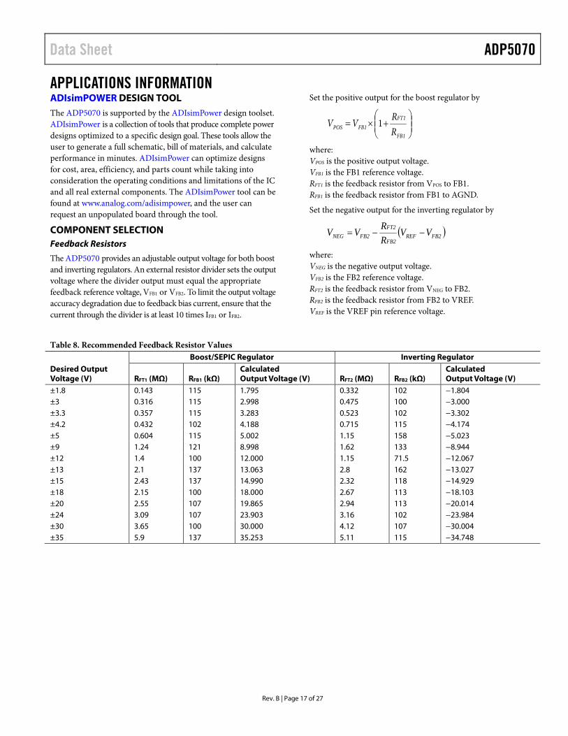
COMPONENT SELECTION Feedback Resistors
The ADP5070 provides an adjustable output voltage for both boost and inverting regulators. An external resistor divider sets the output voltage where the divider output must equal the appropriate feedback reference voltage, VFB1 or VFB2. To limit the output voltage accuracy degradation due to feedback bias current, ensure that the current through the divider is at least 10 times IFB1 or IFB2.
Set the positive output for the boost regulator by
+×=
FB1
FT1FB1POS R
RVV 1
where: VPOS is the positive output voltage. VFB1 is the FB1 reference voltage. RFT1 is the feedback resistor from VPOS to FB1. RFB1 is the feedback resistor from FB1 to AGND.
Set the negative output for the inverting regulator by
( )FB2REFFB2
FT2FB2NEG VV
RRVV −−=
where: VNEG is the negative output voltage. VFB2 is the FB2 reference voltage. RFT2 is the feedback resistor from VNEG to FB2. RFB2 is the feedback resistor from FB2 to VREF. VREF is the VREF pin reference voltage.
Table 8. Recommended Feedback Resistor Values
Desired Output Voltage (V)
Boost/SEPIC Regulator Inverting Regulator
RFT1 (MΩ) RFB1 (kΩ) Calculated Output Voltage (V) RFT2 (MΩ) RFB2 (kΩ)
Calculated Output Voltage (V)
±1.8 0.143 115 1.795 0.332 102 −1.804 ±3 0.316 115 2.998 0.475 100 −3.000 ±3.3 0.357 115 3.283 0.523 102 −3.302 ±4.2 0.432 102 4.188 0.715 115 −4.174 ±5 0.604 115 5.002 1.15 158 −5.023 ±9 1.24 121 8.998 1.62 133 −8.944 ±12 1.4 100 12.000 1.15 71.5 −12.067 ±13 2.1 137 13.063 2.8 162 −13.027 ±15 2.43 137 14.990 2.32 118 −14.929 ±18 2.15 100 18.000 2.67 113 −18.103 ±20 2.55 107 19.865 2.94 113 −20.014 ±24 3.09 107 23.903 3.16 102 −23.984 ±30 3.65 100 30.000 4.12 107 −30.004 ±35 5.9 137 35.253 5.11 115 −34.748
ADP5070 Data Sheet
Rev. B | Page 18 of 27
Output Capacitors
Higher output capacitor values reduce the output voltage ripple and improve load transient response. When choosing this value, it is also important to account for the loss of capacitance due to the output voltage dc bias.
Ceramic capacitors are manufactured with a variety of dielectrics, each with a different behavior over temperature and applied voltage. Capacitors must have a dielectric adequate to ensure the minimum capacitance over the necessary temperature range and dc bias conditions. X5R or X7R dielectrics with a voltage rating of 25 V or 50 V (depending on output) are recommended for best performance. Y5V and Z5U dielectrics are not recommended for use with any dc-to-dc converter because of their poor temperature and dc bias characteristics.
Calculate the worst-case capacitance accounting for capacitor variation over temperature, component tolerance, and voltage using the following equation:
CEFFECTIVE = CNOMINAL × (1 − TEMPCO) × (1 − DCBIASCO) × (1 − Tolerance)
where: CEFFECTIVE is the effective capacitance at the operating voltage. CNOMINAL is the nominal data sheet capacitance. TEMPCO is the worst-case capacitor temperature coefficient. DCBIASCO is the dc bias derating at the output voltage. Tolerance is the worst-case component tolerance.
To guarantee the performance of the device, it is imperative that the effects of dc bias, temperature, and tolerances on the behavior of the capacitors be evaluated for each application.
Capacitors with lower effective series resistance (ESR) and effective series inductance (ESL) are preferred to minimize output voltage ripple.
Note that the use of large output capacitors can require a slower soft start to prevent current limit during startup. A 10 µF capacitor is suggested as a good balance between performance and size.
Input Capacitor
Higher value input capacitors help to reduce the input voltage ripple and improve transient response.
To minimize supply noise, place the input capacitor as close as possible to the PVINSYS pin, PVIN1 pin, and PVIN2 pin. A low ESR capacitor is recommended.
The effective capacitance needed for stability is a minimum of 10 µF. If the power pins are individually decoupled, it is recommended to use an effective minimum of a 5.6 µF capacitor on the PVIN1 and PVIN2 pins and a 3.3 µF capacitor on the PVINSYS pin. The minimum values specified exclude dc bias, temperature, and tolerance effects that are application dependent and must be taken into consideration.
VREG Capacitor
A 1.0 µF ceramic capacitor (CVREG) is required between the VREG pin and AGND.
VREF Capacitor
A 1.0 µF ceramic capacitor (CVREF) is required between the VREF pin and AGND.
Soft Start Resistor
A resistor can be connected between the SS pin and the AGND pin to increase the soft start time. The soft start time can be set by the resistor between 4 ms (268 kΩ) and 32 ms (50 kΩ). Leaving the SS pin open selects the fastest time of 4 ms. Figure 44 shows the behavior of this operation. Calculate the soft start time using the following formula:
tSS = 38.4 × 10⁻³ − 1.28 × 10⁻⁷ × RSS (Ω)
where 50 kΩ ≤ RSS ≤ 268 kΩ.
SS PIN OPEN
SOFT STARTTIMER
SOFT STARTRESISTORR1R2
32ms
4ms
1206
8-04
3
Figure 44. Soft Start Behavior
Diodes
A Schottky diode with low junction capacitance is recommended for D1 and D2. At higher output voltages and especially at higher switching frequencies, the junction capacitance is a significant contributor to efficiency. Higher capacitance diodes also generate more switching noise. As a guide, a diode with less than 40 pF junction capacitance is preferred when the output voltage is above 5 V.
Inductor Selection for the Boost Regulator
The inductor stores energy during the on time of the power switch, and transfers that energy to the output through the output rectifier during the off time. To balance the tradeoffs between small inductor current ripple and efficiency, inductance values in the range of 1 µH to 22 µH are recommended. In general, lower inductance values have higher saturation current and lower series resistance for a given physical size. However, lower inductance results in a higher peak current that can lead to reduced efficiency and greater input and/or output ripple and noise. A peak-to-peak inductor ripple current close to 30% of the maximum dc input current for the application typically yields an optimal compromise.
Data Sheet ADP5070
Rev. B | Page 19 of 27
For the inductor ripple current in continuous conduction mode (CCM) operation, the input (VIN) and output (VPOS) voltages determine the switch duty cycle (DUTY1) by
+
+−=
DIODE1POS
DIODE1INPOS1
VVVVV
DUTY
where VDIODE1 is the forward voltage drop of the Schottky diode (D1).
The dc input current in CCM (IIN) can be determined by the following equation:
)1( 1
OUT1IN DUTY
II
−=
Using the duty cycle (DUTY1) and switching frequency (fSW), determine the on time (tON1) using the following equation:
SW
1ON1 f
DUTYt =
The inductor ripple current (∆IL1) in steady state is calculated by
L1tVI ON1IN
L1×
=∆
Solve for the inductance value (L1) using the following equation:
L1
ON1IN
ItVL1
∆×
=
Assuming an inductor ripple current of 30% of the maximum dc input current results in
OUT1
1ON1IN
IDUTYtV
L1×
−××=
3.0)1(
Ensure that the peak inductor current (the maximum input current plus half the inductor ripple current) is below the rated saturation current of the inductor. Likewise, ensure that the maximum rated rms current of the inductor is greater than the maximum dc input current to the regulator.
When the ADP5070 boost regulator is operated in CCM at duty cycles greater than 50%, slope compensation is required to stabilize the current mode loop. This slope compensation is built in to the ADP5070. For stable current mode operation, ensure that the selected inductance is equal to or greater than the minimum calculated inductance, LMIN1, for the application parameters in the following equation:
−
−×=> 33.0
)1(27.0
1INMIN1 DUTY
VLL1 (µH)
Table 10 suggests a series of inductors to use with the ADP5070 boost regulator.
Inductor Selection for the Inverting Regulator
The inductor stores energy during the on time of the power switch, and transfers that energy to the output through the output rectifier during the off time. To balance the tradeoffs between small inductor current ripple and efficiency, inductance values in the range of 1 µH to 22 µH are recommended. In general, lower inductance values have higher saturation current and lower series resistance for a given physical size. However, lower inductance results in a higher peak current that can lead to reduced efficiency and greater input and/or output ripple and noise. A peak-to-peak inductor ripple current close to 30% of the maximum dc current in the inductor typically yields an optimal compromise.
For the inductor ripple current in continuous conduction mode (CCM) operation, the input (VIN) and output (VNEG) voltages determine the switch duty cycle (DUTY2) by
++
+=
DIODE2NEGIN
DIODE2NEG2
VVVVV
DUTY||
||
where VDIODE2 is the forward voltage drop of the Schottky diode (D2).
The dc current in the inductor in CCM (IL2) can be determined by the following equation:
)1( 2
OUT2L2 DUTY
II
−=
Using the duty cycle (DUTY2) and switching frequency (fSW), determine the on time (tON2) by the following equation:
SW
2ON2 f
DUTYt =
The inductor ripple current (∆IL2) in steady state is calculated by
L2tV
I ON2INL2
×=∆
Solve for the inductance value (L2) by the following equation:
L2
ON2IN
ItVL2
∆×
=
Assuming an inductor ripple current of 30% of the maximum dc current in the inductor results in
OUT2
2ON2IN
IDUTYtV
L2×
−××=
3.0)1(
Ensure that the peak inductor current (the maximum input current plus half the inductor ripple current) is below the rated saturation current of the inductor. Likewise, ensure that the maximum rated rms current of the inductor is greater than the maximum dc input current to the regulator.

ADP5070 Data Sheet
Rev. B | Page 20 of 27
When the ADP5070 inverting regulator is operated in CCM at duty cycles greater than 50%, slope compensation is required to stabilize the current mode loop. For stable current mode operation, ensure that the selected inductance is equal to or greater than the minimum calculated inductance, LMIN2, for the application parameters in the following equation:
−
−×=> 33.0
)1(27.0
2INMIN2 DUTY
VLL2 (µH)
Table 11 suggests a series of inductors to use with the ADP5070 inverting regulator.
LOOP COMPENSATION The ADP5070 uses external components to compensate the regulator loop, allowing the optimization of the loop dynamics for a given application. It is recommended to use the ADIsimPower tool to calculate compensation components.
Boost Regulator
The boost converter produces an undesirable right half plane zero in the regulation feedback loop. This feedback loop requires compensating the regulator such that the crossover frequency occurs well below the frequency of the right half plane zero. The right half plane zero is determined by the following equation:
L1DUTYR
RHPf1LOAD1
Z1 ×−
=π2
)1()(
2
where: fZ1(RHP) is the right half plane zero frequency. RLOAD1 is the equivalent load resistance or the output voltage divided by the load current.
+
+−=
DIODE1POS
DIODE1INPOS1
VVVVV
DUTY
where VDIODE1 is the forward voltage drop of the Schottky diode (D1).
To stabilize the regulator, ensure that the regulator crossover frequency is less than or equal to one-tenth of the right half plane zero frequency.
The boost regulator loop gain is
OUT1CS1
COMP1OUT1M1POS
IN
POS
FB1VL1
ZG
Z||RGVV
VV
A
×
××××=
where: AVL1 is the loop gain. VFB1 is the feedback regulation voltage VPOS is the regulated positive output voltage. VIN is the input voltage. GM1 is the error amplifier transconductance gain. ROUT1 is the output impedance of the error amplifier and is 33 MΩ.
ZCOMP1 is the impedance of the series RC network from COMP1 to AGND. GCS1 is the current sense transconductance gain (the inductor current divided by the voltage at COMP1), which is internally set by the ADP5070 and is 6.25 A/V. ZOUT1 is the impedance of the load in parallel with the output capacitor.
To determine the crossover frequency (fC1), it is important to note that, at that frequency, the compensation impedance (ZCOMP1) is dominated by a resistor (RC1), and the output impedance (ZOUT1) is dominated by the impedance of an output capacitor (COUT1).
Therefore, when solving for the crossover frequency, the equation (by definition of the crossover frequency) is simplified to
12
1=
××
×××××=
OUT1C1
CS1C1M1POS
IN
POS
FB1VL1
Cfπ
GRGVV
VVA
where fC1 is the crossover frequency.
To solve for RC1, use the following equation:
CS1M1INFB1
POSOUT1C1C1 GGVV
(VCfR×××
×××=
2)2π
where GCS1 = 6.25 A/V.
Using typical values for VFB1 and GM1 results in
IN
POSOUT1C1C1 V
(VCfR
2)4188 ×××=
For better accuracy, it is recommended to use the value of output capacitance, COUT1, expected for the dc bias conditions under which it operates under in the calculation for RC1.
After the compensation resistor is known, set the zero formed by the compensation capacitor and resistor to one-fourth of the crossover frequency, or
C1C1C1 Rfπ
C××
=2
where CC1 is the compensation capacitor value. ERROR
AMPLIFIER
REF1gM1
FB1COMP1
RC1CB1
CC1
1206
8-04
4
Figure 45. Compensation Components
The capacitor, CB1, is chosen to cancel the zero introduced by the output capacitor ESR. Solve for CB1 as follows:
C1
OUT1B1
RCESRC ×
=
Data Sheet ADP5070
Rev. B | Page 21 of 27
For low ESR output capacitance such as with a ceramic capacitor, CB1 is optional. For optimal transient performance, RC1 and CC1 may need to be adjusted by observing the load transient response of the ADP5070. For most applications, RC1 must be within the range of 1 kΩ to 200 kΩ, and CC1 must be within the range of 1 nF to 68 nF.
Inverting Regulator
The inverting converter, like the boost converter, produces an undesirable right half plane zero in the regulation feedback loop. This feedback loop requires compensating the regulator such that the crossover frequency occurs well below the frequency of the right half plane zero. The right half plane zero frequency is determined by the following equation:
2
22LOAD2
Z2 DUTYL2π)DUTY(R(RHP)f
××−
=2
1
where: fZ2(RHP) is the right half plane zero frequency. RLOAD2 is the equivalent load resistance or the output voltage divided by the load current.
++
+=
DIODE2NEGIN
DIODE2NEG2
V||VVV||V
DUTY
where VDIODE2 is the forward voltage drop of the Schottky diode (D2).
To stabilize the regulator, ensure that the regulator crossover frequency is less than or equal to one-tenth of the right half plane zero frequency.
The regulator loop gain is
OUT2CS2COMP2OUT2
M2NEGIN
IN
NEG
FB2VL2
ZGZ||R
GVV
V||V
VA
××
×××+
×=|)|2(
where: AVL2 is the loop gain. VFB2 is the feedback regulation voltage. VNEG is the regulated negative output voltage. VIN is the input voltage. GM2 is the error amplifier transconductance gain. ROUT2 is the output impedance of the error amplifier and is 33 MΩ. ZCOMP2 is the impedance of the series RC network from COMP2 to AGND. GCS2 is the current sense transconductance gain (the inductor current divided by the voltage at COMP2), which is internally set by the ADP5070 and is 6.25 A/V. ZOUT2 is the impedance of the load in parallel with the output capacitor.
To determine the crossover frequency, it is important to note that, at that frequency, the compensation impedance (ZCOMP2) is dominated by a resistor, RC2, and the output impedance (ZOUT2) is dominated by the impedance of the output capacitor, COUT2. Therefore, when solving for the crossover frequency, the equation (by definition of the crossover frequency) is simplified to
12
12
|)|2(
=××
××
×××+
×=
OUT2C2CSC2
M2NEGIN
IN
NEG
FB2VL2
CfπGR
GVV
V||V
VA
where fC2 is the crossover frequency.
To solve for RC2, use the following equation:
CS2M2INFB2
NEGINNEGOUT2C2C2 GGVV
V(V||VCfπR
×××
×+××××=
|)|2(2
where GCS2 = 6.25 A/V.
Using typical values for VFB2 and GM2 results in
IN
NEGINNEGOUTC2C2 V
VVVCfR
|)|2((||4188 2 ×+××××=
For better accuracy, it is recommended to use the value of output capacitance, COUT2, expected under the dc bias conditions that it operates under in the calculation for RC2.
After the compensation resistor is known, set the zero formed by the CC2 and RC2 to one-fourth of the crossover frequency, or
C2C2
C2Rfπ
C××
=2
where CC2 is the compensation capacitor.
ERRORAMPLIFIER
REF2gM2
FB2COMP2
RC2CB2
CC212
068-
045
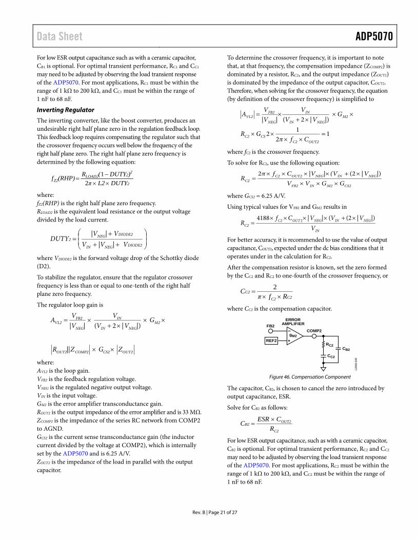
Figure 46. Compensation Component
The capacitor, CB2, is chosen to cancel the zero introduced by output capacitance, ESR.
Solve for CB2 as follows:
C2
OUT2B2
RCESR
C×
=
For low ESR output capacitance, such as with a ceramic capacitor, CB2 is optional. For optimal transient performance, RC2 and CC2 may need to be adjusted by observing the load transient response of the ADP5070. For most applications, RC2 must be within the range of 1 kΩ to 200 kΩ, and CC2 must be within the range of 1 nF to 68 nF.
ADP5070 Data Sheet
Rev. B | Page 22 of 27
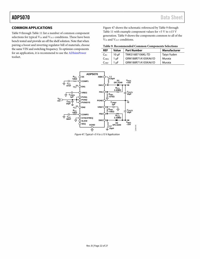
COMMON APPLICATIONS Table 9 through Table 11 list a number of common component selections for typical VIN and VOUT conditions. These have been bench tested and provide an off the shelf solution. Note that when pairing a boost and inverting regulator bill of materials, choose the same VIN and switching frequency. To optimize components for an application, it is recommend to use the ADIsimPower toolset.
Figure 47 shows the schematic referenced by Table 9 through Table 11 with example component values for +5 V to ±15 V generation. Table 9 shows the components common to all of the VIN and VOUT conditions.
Table 9. Recommended Common Components Selections REF Value Part Number Manufacturer CIN1 10 µF TMK316B7106KL-TD Taiyo Yuden CVREG 1 µF GRM188R71A105KA61D Murata CVREF 1 µF GRM188R71A105KA61D Murata
ADP5070SS INBK
SW1
COMP1
RC112kΩ
CC147nF
COMP2
RC215kΩ
CC268nF
CVREG1µF
VREG
EN1
SYNC/FREQSLEWSEQ
EN2
AGND
PVIN1PVIN2PVINSYSCIN1
10µF
VIN+5V
FB1
D1DFLS240
L16.8µH
L215µH
RFB1137kΩ
RFT12.43MΩ
VPOS+15V
SW2
PGND
FB2
VREF
D2DFLS240
RFB2118kΩ
VNEG–15V
CVREF1µF
COUT110µF
COUT210µF
RFT22.32MΩ
1206
8-04
6
Figure 47. Typical +5 V to ±15 V Application

Data Sheet ADP5070
Rev. B | Page 23 of 27
Table 10. Recommended Boost Regulator Components
VIN (V)
VPOS (V)
Freq. (MHz)
L1 (µH)
L1 Manufacturer Part Number
COUT1 (µF) COUT1, Murata Part
D1, Diodes, Inc. Part
RFT1 (MΩ)
RFB1 (kΩ)
CC1 (nF)
RC1 (kΩ) Coilcraft®
Wurth Elektronik
3.3 5 1.2 3.3 XAL4030-332ME_ 10 GRM32ER71H106KA12L DFLS240L 0.604 115 47 4.7 3.3 5 2.4 2.2 XAL4020-222ME_ 74438356022 10 GRM32ER71H106KA12L DFLS240L 0.604 115 47 4.7 3.3 9 1.2 4.7 XAL4030-472ME_ 74438357047 10 GRM32ER71H106KA12L DFLS240 1.24 121 47 6.8 3.3 9 2.4 2.2 XAL4020-222ME_ 74438356022 10 GRM32ER71H106KA12L DFLS240 1.24 121 47 6.8 3.3 15 1.2 6.8 XAL4030-682ME_ 74438357068 10 GRM32ER71H106KA12L DFLS240 2.43 137 47 22 3.3 15 2.4 4.7 XAL4030-472ME_ 74438357047 10 GRM32ER71H106KA12L DFLS240 2.43 137 47 25 3.3 24 1.2 6.8 XAL4030-682ME_ 74438357068 10 GRM32ER71H106KA12L DFLS240 3.09 107 47 33 3.3 24 2.4 6.8 XAL4030-682ME_ 74438357068 10 GRM32ER71H106KA12L DFLS240 3.09 107 47 33 3.3 34 1.2 6.8 XAL4030-682ME_ 74438357068 10 GRM32ER71H106KA12L DFLS240 4.22 102 47 27 3.3 34 2.4 10 XAL4040-103ME_ 10 GRM32ER71H106KA12L DFLS240 4.22 102 47 27 5 9 1.2 4.7 XAL4030-472ME_ 74438357047 10 GRM32ER71H106KA12L DFLS240 1.24 121 47 3.3 5 9 2.4 3.3 XAL4030-332ME_ 10 GRM32ER71H106KA12L DFLS240 1.24 121 47 3.9 5 15 1.2 6.8 XAL4030-682ME_ 74438357068 10 GRM32ER71H106KA12L DFLS240 2.43 137 47 12 5 15 2.4 3.3 XAL4030-332ME_ 10 GRM32ER71H106KA12L DFLS240 2.43 137 47 15 5 24 1.2 10 XAL4040-103ME_ 10 GRM32ER71H106KA12L DFLS240 3.09 107 47 18 5 24 2.4 4.7 XAL4030-472ME_ 74438357047 10 GRM32ER71H106KA12L DFLS240 3.09 107 47 18 5 34 1.2 10 XAL4040-103ME_ 10 GRM32ER71H106KA12L DFLS240 4.22 102 47 18 5 34 2.4 10 XAL4040-103ME_ 10 GRM32ER71H106KA12L DFLS240 4.22 102 47 18 12 24 1.2 15 XAL4040-153ME_ 10 GRM32ER71H106KA12L DFLS240 3.09 107 47 12 12 24 2.4 6.8 XAL4030-682ME_ 74438357068 10 GRM32ER71H106KA12L DFLS240 3.09 107 47 12
Table 11. Recommended Inverting Regulator Components
VIN (V)
VNEG (V)
Freq. (MHz)
L2 (µH)
L2, Manufacturer Part Number COUT2 (µF) COUT2, Murata Part
D2, Diodes, Inc. Part
RFT2 (MΩ)
RFB2 (kΩ)
CC2 (nF)
RC2 (kΩ) Coilcraft
Wurth Elektronik
3.3 −5 1.2 6.8 XAL4030-682ME_ 74438357068 10 GRM32ER71H106KA12L DFLS240L 1.15 158 47 4.7 3.3 −5 2.4 4.7 XAL4030-472ME_ 74438357047 10 GRM32ER71H106KA12L DFLS240L 1.15 158 47 6.8 3.3 −9 1.2 10 XAL4040-103ME_ 10 GRM32ER71H106KA12L DFLS240 1.62 133 47 8.2 3.3 −9 2.4 4.7 XAL4030-472ME_ 74438357047 10 GRM32ER71H106KA12L DFLS240 1.62 133 47 8.2 3.3 −15 1.2 10 XAL4040-103ME_ 10 GRM32ER71H106KA12L DFLS240 2.32 118 47 12 3.3 −15 2.4 4.7 XAL4030-472ME_ 74438357047 10 GRM32ER71H106KA12L DFLS240 2.32 118 47 18 3.3 −24 1.2 10 XAL4040-103ME_ 10 GRM32ER71H106KA12L DFLS240 3.16 102 47 22 3.3 −24 2.4 6.8 XAL4030-682ME_ 74438357068 10 GRM32ER71H106KA12L DFLS240 3.16 102 47 33 3.3 −34 1.2 10 XAL4040-103ME_ 10 GRM32ER71H106KA12L DFLS240 4.99 115 47 47 3.3 −34 2.4 10 XAL4040-103ME_ 10 GRM32ER71H106KA12L DFLS240 4.99 115 47 47 5 −9 1.2 10 XAL4040-103ME_ 10 GRM32ER71H106KA12L DFLS240 1.62 133 47 8.2 5 −9 2.4 6.8 XAL4030-682ME_ 74438357068 10 GRM32ER71H106KA12L DFLS240 1.62 133 47 8.2 5 −15 1.2 15 XAL4040-153ME_ 10 GRM32ER71H106KA12L DFLS240 2.32 118 68 15 5 −15 2.4 6.8 XAL4030-682ME_ 74438357068 10 GRM32ER71H106KA12L DFLS240 2.32 118 47 22 5 −24 1.2 15 XAL4040-153ME_ 10 GRM32ER71H106KA12L DFLS240 3.16 102 47 22 5 −24 2.4 6.8 XAL4030-682ME_ 74438357068 10 GRM32ER71H106KA12L DFLS240 3.16 102 47 22 5 −34 1.2 15 XAL4040-153ME_ 10 GRM32ER71H106KA12L DFLS240 4.99 115 47 39 5 −34 2.4 10 XAL4040-103ME_ 10 GRM32ER71H106KA12L DFLS240 4.99 115 47 39 12 −24 1.2 22 XAL5050-223ME_ 10 GRM32ER71H106KA12L DFLS240 3.16 102 47 10 12 −24 2.4 15 XAL4040-153ME_ 10 GRM32ER71H106KA12L DFLS240 3.16 102 47 10

ADP5070 Data Sheet
Rev. B | Page 24 of 27
SUPER LOW NOISE WITH OPTIONAL LDOS Low dropout regulators (LDOs) can be added to the ADP5070 output to provide super low noise supplies for high performance ADCs, digital-to-analog converters (DACs), and other precision applications. Table 12 shows recommended companion devices, and Figure 48 shows a typical application schematic for ±15 V generation from a +5 V supply.
ADP5070SS INBK
SW1
COMP1
RC15.6kΩ
CC147nF
COMP2
RC212kΩ
CC247nF
CVREG1µF
VREG
EN1
SYNC/FREQSLEWSEQ
EN2
AGND
PVIN1PVIN2PVINSYSCIN1
10µF
VIN+5V
FB1
D1DFLS240
L13.3µH
L26.8µH
RFB1113kΩ
RFT12.15MΩ
+16V
SW2
PGND
FB2
VREF
D2DFLS240
RFB2100kΩ
–16V
VPOS = +15V
VNEG = –15V
CVREF1µF
COUT110µF
COUT210µF
RFT22.1MΩ
ENGND
CSS31nF
VIN VOUT
ADJ(5V)
SS
ADP7142
RFB310kΩ
RFT320kΩ
CNR31µF COUT3
2.2µFRNR31kΩ
EN
GNDVIN
VOUT
ADJ
ADP7182
RFB459kΩ
RFT452.3kΩ
CNR447µF COUT4
2.2µFRNR45.9kΩ
CIN31µF
CIN42.2µF
1206
8-04
7
Figure 48. Super Low Noise ±15 V Generation with Post Regulation by the ADP7142 (+40 V, +200 mA, Low Noise LDO) and ADP7182 (−28 V, −200 mA, Low Noise LDO)
Table 12. Recommended LDOs for Super Low Noise Operation Parameter ADP7102 ADP7104 ADP7105 ADP7118 ADP7142 ADP7182 VIN Range 3.3 V to 20 V 3.3 V to 20 V 3.3 V to 20 V 2.7 V to 20 V 2.7 V to 40 V −2.7 V to −28 V Fixed VOUT 1.5 V to 9 V 1.5 V to 9 V 1.8 V, 3.3 V, 5 V 1.2 V to 5 V 1.2 V to 5 V −1.8 V to −5 V Adjustable VOUT 1.22 V to 19 V 1.22 V to 19 V 1.22 V to 19 V 1.2 V to 19 V 1.2 V to 39 V −1.22 V to−27 V IOUT 300 mA 500 mA 500 mA 200 mA 200 mA −200 mA IQ at No Load 400 µA 400 µA 400 µA 50 µA 50 µA −33 µA ISHDN Typical 40 µA 40 µA 40 µA 2 µA 2 µA −2 µA Soft Start No No Yes Yes Yes No PGOOD Yes Yes Yes No No No Noise (Fixed), 10 Hz
to 100 kHz 15 µV rms 15 µV rms 15 µV rms 11 µV rms 11 µV rms 18 µV rms
PSRR (100 kHz) 60 dB 60 dB 60 dB 68 dB 68 dB 45 dB PSRR (1 MHz) 40 dB 40 dB 40 dB 50 dB 50 dB 45 dB Package 8-lead LFCSP,
8-lead SOIC 8-lead LFCSP, 8-lead SOIC
8-lead LFCSP, 8-lead SOIC
6-lead LFCSP, 8-lead SOIC, 5-lead TSOT
6-lead LFCSP, 8-lead SOIC, 5-lead TSOT
6-lead LFCSP, 8-lead LFCSP, 5-lead TSOT

Data Sheet ADP5070
Rev. B | Page 25 of 27
SEPIC STEP-UP/STEP-DOWN OPERATION SEPIC operation allows the positive output channel to produce a voltage higher or lower than VIN. Both standalone and coupled inductors are supported for this application. SEPIC designs are supported in the ADIsimPower toolset.
ADP5070SS INBK
SW1
RC1
CC1COMP1
RC2
CC2COMP2
CVREG
1µFVREG
EN1
SYNC/FREQSLEWSEQ
EN2
AGND
PVIN1PVIN2PVINSYSCIN1
10µF
VIN = +12V
FB1
D1
L1A L1B
L2
RFB1
RFT1
+5V/400mA
SW2
PGND
FB2
VREF
D2
RFB2
RFT2
–5V/400mA
CVREF
1µF
CS1
COUT1
COUT2
STANDALONE ORCOUPLED-INDUCTOR
1206
8-04
8
Figure 49. SEPIC Application for +12 V in to ±5 V Output Generation
ADP5070 Data Sheet
Rev. B | Page 26 of 27
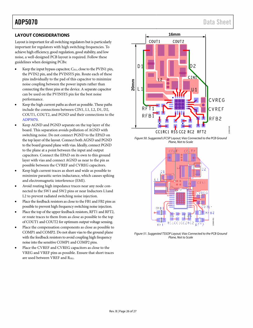
LAYOUT CONSIDERATIONS Layout is important for all switching regulators but is particularly important for regulators with high switching frequencies. To achieve high efficiency, good regulation, good stability, and low noise, a well-designed PCB layout is required. Follow these guidelines when designing PCBs:
• Keep the input bypass capacitor, CIN1, close to the PVIN1 pin, the PVIN2 pin, and the PVINSYS pin. Route each of these pins individually to the pad of this capacitor to minimize noise coupling between the power inputs rather than connecting the three pins at the device. A separate capacitor can be used on the PVINSYS pin for the best noise performance.
• Keep the high current paths as short as possible. These paths include the connections between CIN1, L1, L2, D1, D2, COUT1, COUT2, and PGND and their connections to the ADP5070.
• Keep AGND and PGND separate on the top layer of the board. This separation avoids pollution of AGND with switching noise. Do not connect PGND to the EPAD on the top layer of the layout. Connect both AGND and PGND to the board ground plane with vias. Ideally, connect PGND to the plane at a point between the input and output capacitors. Connect the EPAD on its own to this ground layer with vias and connect AGND as near to the pin as possible between the CVREF and CVREG capacitors.
• Keep high current traces as short and wide as possible to minimize parasitic series inductance, which causes spiking and electromagnetic interference (EMI).
• Avoid routing high impedance traces near any node con-nected to the SW1 and SW2 pins or near Inductors L1and L2 to prevent radiated switching noise injection.
• Place the feedback resistors as close to the FB1 and FB2 pins as possible to prevent high frequency switching noise injection.
• Place the top of the upper feedback resistors, RFT1 and RFT2, or route traces to them from as close as possible to the top of COUT1 and COUT2 for optimum output voltage sensing.
• Place the compensation components as close as possible to COMP1 and COMP2. Do not share vias to the ground plane with the feedback resistors to avoid coupling high frequency noise into the sensitive COMP1 and COMP2 pins.
• Place the CVREF and CVREG capacitors as close to the VREG and VREF pins as possible. Ensure that short traces are used between VREF and RFB2.
16mm
20m
m
1206
8-04
9
Figure 50. Suggested LFCSP Layout; Vias Connected to the PCB Ground
Plane, Not to Scale
1206
8-05
1
Figure 51. Suggested TSSOP Layout; Vias Connected to the PCB Ground
Plane, Not to Scale

Data Sheet ADP5070
Rev. B | Page 27 of 27
OUTLINE DIMENSIONS
0.50BSC
0.500.400.30
0.300.250.18
COMPLIANT TO JEDEC STANDARDS MO-220-WGGD-11.
4.104.00 SQ3.90
0.800.750.70 0.05 MAX
0.02 NOM
0.20 REF
0.25 MIN
COPLANARITY0.08
PIN 1INDICATOR
2.752.60 SQ2.35
1
20
610
11
15
16
5
BOTTOM VIEWTOP VIEW
SIDE VIEWFOR PROPER CONNECTION OFTHE EXPOSED PAD, REFER TOTHE PIN CONFIGURATION ANDFUNCTION DESCRIPTIONSSECTION OF THIS DATA SHEET.
02-2
1-20
17-B
EXPOSEDPAD
PKG
-005
089
SEATINGPLANE
PIN 1INDIC ATOR AREA OPTIONS(SEE DETAIL A)
DETAIL A(JEDEC 95)
Figure 52. 20-Lead Lead Frame Chip Scale Package [LFCSP]
4 mm × 4 mm Body and 0.75 mm Package Height (CP-20-8)
Dimensions shown in millimeters
COMPLIANT TO JEDEC STANDARDS MO-153-ACT 05-0
8-20
06-A
20 11
101
EXPOSEDPAD
(Pins Up)
6.606.506.40
4.504.404.30
6.40BSC
TOPVIEW
BOTTOM VIEW0.65 BSC
0.150.05
COPLANARITY0.10
1.20 MAX1.051.000.80
0.300.19
SEATINGPLANE
0.200.09
3.053.002.95
8°0°
0.750.600.45
4.254.204.15
FOR PROPER CONNECTION OFTHE EXPOSED PAD, REFER TOTHE PIN CONFIGURATION ANDFUNCTION DESCRIPTIONSSECTION OF THIS DATA SHEET.
Figure 53. 20-Lead Thin Shrink Small Outline With Exposed Pad [TSSOP_EP]
(RE-20-1) Dimensions shown in millimeters
ORDERING GUIDE Model1 Temperature Range Package Description Package Option ADP5070ACPZ −40°C to +125°C 20-Lead Lead Frame Chip Scale Package [LFCSP] CP-20-8 ADP5070ACPZ-R7 −40°C to +125°C 20-Lead Lead Frame Chip Scale Package [LFCSP] CP-20-8 ADP5070AREZ −40°C to +125°C 20-Lead Thin Shrink Small Outline With Exposed Pad [TSSOP_EP] RE-20-1 ADP5070AREZ-R7 −40°C to +125°C 20-Lead Thin Shrink Small Outline With Exposed Pad [TSSOP_EP] RE-20-1 ADP5070CP-EVALZ Evaluation Board for the LFCSP ADP5070RE-EVALZ Evaluation Board for the TSSOP_EP 1 Z = RoHS Compliant Part.
©2015–2017 Analog Devices, Inc. All rights reserved. Trademarks and registered trademarks are the property of their respective owners. D12068-0-7/17(B)