1.2 A, DC-to-DC Inverting Regulator · 1.2 A, DC-to-DC Inverting Regulator Data Sheet ADP5073 Rev....
17
1.2 A, DC-to-DC Inverting Regulator Data Sheet ADP5073 Rev. A Document Feedback Information furnished by Analog Devices is believed to be accurate and reliable. However, no responsibility is assumed by Analog Devices for its use, nor for any infringements of patents or other rights of third parties that may result from its use. Specifications subject to change without notice. No license is granted by implication or otherwise under any patent or patent rights of Analog Devices. Trademarks and registered trademarks are the property of their respective owners. One Technology Way, P.O. Box 9106, Norwood, MA 02062-9106, U.S.A. Tel: 781.329.4700 ©2015–2017 Analog Devices, Inc. All rights reserved. Technical Support www.analog.com FEATURES Wide input voltage range: 2.85 V to 15 V Adjustable negative output to VIN − 39 V Integrated 1.2 A main switch 1.2 MHz/2.4 MHz switching frequency with optional external frequency synchronization from 1.0 MHz to 2.6 MHz Resistor programmable soft start timer Slew rate control for lower system noise Precision enable control Power-good output UVLO, OCP, OVP, and TSD protection 3 mm × 3 mm, 16-lead LFCSP −40°C to +125°C junction temperature Supported by the ADIsimPower tool set APPLICATIONS Bipolar amplifiers, ADCs, digital-to-analog converters (DACs), and multiplexers High speed converters Radio frequency (RF) power amplifier (PA) bias Optical modules TYPICAL APPLICATION CIRCUIT R C C C V IN L1 D1 R FB C VREF C VREG R FT ADP5073 COMP VREG SS EN GND AVIN PVIN SLEW SYNC/FREQ FB SW VREF V OUT C OUT ON OFF PWRGD PWRGD C IN R PG 12817-001 Figure 1. GENERAL DESCRIPTION The ADP5073 is a high performance dc-to-dc inverting regulator used to generate negative supply rails. The input voltage range of 2.85 V to 15 V supports a wide variety of applications. The integrated main switch enables the generation of an adjustable negative output voltage down to 39 V below the input voltage. The ADP5073 operates at a pin selected 1.2 MHz/2.4 MHz switching frequency. The ADP5073 can synchronize with an external oscillator from 1.0 MHz to 2.6 MHz to ease noise filtering in sensitive applications. The regulator implements programmable slew rate control circuitry for the MOSFET driver stage to reduce electromagnetic interference (EMI). The ADP5073 includes a fixed internal or resistor programmable soft start timer to prevent inrush current at power-up. During shutdown, the regulator completely disconnects the load from the input supply to provide a true shutdown. A power-good pin is available to indicate the output is stable. Other key safety features in the ADP5073 include overcurrent protection (OCP), overvoltage protection (OVP), thermal shutdown (TSD), and input undervoltage lockout (UVLO). The ADP5073 is available in a 16-lead LFCSP and is rated for a −40°C to +125°C operating junction temperature range. Table 1. Related Devices Device Boost Switch (A) Inverter Switch (A) Package ADP5070 1.0 0.6 20-lead LFCSP (4 mm × 4 mm) and TSSOP ADP5071 2.0 1.2 20-lead LFCSP (4 mm × 4 mm) and TSSOP ADP5073 Not applicable 1.2 16-lead LFCSP (3 mm × 3 mm) ADP5074 Not applicable 2.4 16-lead LFCSP (3 mm × 3 mm) ADP5075 Not applicable 0.8 12-ball WLCSP (1.61 mm × 2.18 mm)
Transcript of 1.2 A, DC-to-DC Inverting Regulator · 1.2 A, DC-to-DC Inverting Regulator Data Sheet ADP5073 Rev....

1.2 A, DC-to-DC Inverting Regulator Data Sheet ADP5073
Rev. A Document Feedback Information furnished by Analog Devices is believed to be accurate and reliable. However, no responsibility is assumed by Analog Devices for its use, nor for any infringements of patents or other rights of third parties that may result from its use. Specifications subject to change without notice. No license is granted by implication or otherwise under any patent or patent rights of Analog Devices. Trademarks and registered trademarks are the property of their respective owners.
One Technology Way, P.O. Box 9106, Norwood, MA 02062-9106, U.S.A. Tel: 781.329.4700 ©2015–2017 Analog Devices, Inc. All rights reserved. Technical Support www.analog.com
FEATURES Wide input voltage range: 2.85 V to 15 V Adjustable negative output to VIN − 39 V Integrated 1.2 A main switch 1.2 MHz/2.4 MHz switching frequency with optional external
frequency synchronization from 1.0 MHz to 2.6 MHz Resistor programmable soft start timer Slew rate control for lower system noise Precision enable control Power-good output UVLO, OCP, OVP, and TSD protection 3 mm × 3 mm, 16-lead LFCSP −40°C to +125°C junction temperature Supported by the ADIsimPower tool set
APPLICATIONS Bipolar amplifiers, ADCs, digital-to-analog converters
(DACs), and multiplexers High speed converters Radio frequency (RF) power amplifier (PA) bias Optical modules
TYPICAL APPLICATION CIRCUIT
RC
CC
VIN
L1
D1
RFB
CVREF
CVREG
RFTADP5073
COMP
VREG
SS
EN
GND
AVIN
PVIN
SLEW
SYNC/FREQ
FB
SW
VREF
VOUT
COUT
ONOFF
PWRGDPWRGD
CIN
RPG
1281
7-00
1
Figure 1.
GENERAL DESCRIPTION The ADP5073 is a high performance dc-to-dc inverting regulator used to generate negative supply rails.
The input voltage range of 2.85 V to 15 V supports a wide variety of applications. The integrated main switch enables the generation of an adjustable negative output voltage down to 39 V below the input voltage.
The ADP5073 operates at a pin selected 1.2 MHz/2.4 MHz switching frequency. The ADP5073 can synchronize with an external oscillator from 1.0 MHz to 2.6 MHz to ease noise filtering in sensitive applications. The regulator implements programmable slew rate control circuitry for the MOSFET driver stage to reduce electromagnetic interference (EMI).
The ADP5073 includes a fixed internal or resistor programmable soft start timer to prevent inrush current at power-up. During shutdown, the regulator completely disconnects the load from the input supply to provide a true shutdown. A power-good pin is available to indicate the output is stable.
Other key safety features in the ADP5073 include overcurrent protection (OCP), overvoltage protection (OVP), thermal shutdown (TSD), and input undervoltage lockout (UVLO).
The ADP5073 is available in a 16-lead LFCSP and is rated for a −40°C to +125°C operating junction temperature range.
Table 1. Related Devices
Device Boost Switch (A)
Inverter Switch (A) Package
ADP5070 1.0 0.6 20-lead LFCSP (4 mm × 4 mm) and TSSOP
ADP5071 2.0 1.2 20-lead LFCSP (4 mm × 4 mm) and TSSOP
ADP5073 Not applicable
1.2 16-lead LFCSP (3 mm × 3 mm)
ADP5074 Not applicable
2.4 16-lead LFCSP (3 mm × 3 mm)
ADP5075 Not applicable
0.8 12-ball WLCSP (1.61 mm × 2.18 mm)

ADP5073 Data Sheet
Rev. A | Page 2 of 17
TABLE OF CONTENTS Features .............................................................................................. 1 Applications ....................................................................................... 1 Typical Application Circuit ............................................................. 1 General Description ......................................................................... 1 Revision History ............................................................................... 2 Specifications ..................................................................................... 3 Absolute Maximum Ratings ............................................................ 5
Thermal Resistance ...................................................................... 5 ESD Caution .................................................................................. 5
Pin Configuration and Function Descriptions ............................. 6 Typical Performance Characteristics ............................................. 7 Theory of Operation ...................................................................... 10
PWM Mode ................................................................................. 10 Skip Mode .................................................................................... 10 Undervoltage Lockout (UVLO) ............................................... 10 Oscillator and Synchronization ................................................ 10
Internal Regulators ..................................................................... 10 Precision Enabling...................................................................... 11 Soft Start ...................................................................................... 11 Slew Rate Control ....................................................................... 11 Current-Limit Protection ............................................................ 11 Overvoltage Protection .............................................................. 11 Power Good ................................................................................ 11 Thermal Shutdown .................................................................... 11
Applications Information .............................................................. 12 ADIsimPower Design Tool ....................................................... 12 Component Selection ................................................................ 12 Common Applications .............................................................. 15 Layout Considerations ............................................................... 16
Outline Dimensions ....................................................................... 17 Ordering Guide .......................................................................... 17
REVISION HISTORY 10/2017—Rev. 0 to Rev. A Updated Outline Dimensions ....................................................... 17 Changes to Ordering Guide .......................................................... 17
10/2015—Revision 0: Initial Version

Data Sheet ADP5073
Rev. A | Page 3 of 17
SPECIFICATIONS PVIN = AVIN = 2.85 V to 15 V, VOUT = −15 V, fSW = 1200 kHz, TJ = −40°C to +125°C for minimum/maximum specifications, and
TA = 25°C for typical specifications, unless otherwise noted.
Table 2. Parameter Symbol Min Typ Max Unit Test Conditions/Comments INPUT SUPPLY VOLTAGE RANGE VIN 2.85 15 V PVIN, AVIN QUIESCENT CURRENT
Operating Quiescent Current PVIN, AVIN (Total) IQ 1.8 4.0 mA No switching, EN = high, PVIN = AVIN =
5 V Shutdown Current ISHDN 5 10 µA No switching, EN = low, PVIN = AVIN =
5 V, −40°C ≤ TJ ≤ +85°C UVLO
System UVLO Threshold AVIN Rising VUVLO_RISING 2.8 2.85 V Falling VUVLO_FALLING 2.5 2.55 V
Hysteresis VHYS 0.25 V OSCILLATOR CIRCUIT
Switching Frequency fSW 1.130 1.200 1.270 MHz SYNC/FREQ = low 2.240 2.400 2.560 MHz SYNC/FREQ = high (connect to VREG)
SYNC/FREQ Input Input Clock Range fSYNC 1.000 2.600 MHz Input Clock Minimum On Pulse Width tSYNC_MIN_ON 100 ns Input Clock Minimum Off Pulse Width tSYNC_MIN_OFF 100 ns Input Clock High Logic VH (SYNC) 1.3 V Input Clock Low Logic VL (SYNC) 0.4 V
PRECISION ENABLING (EN) High Level Threshold VTH_H 1.125 1.15 1.175 V Low Level Threshold VTH_L 1.025 1.05 1.075 V Shutdown Mode VTH_S 0.4 V Internal circuitry disabled to achieve ISHDN Pull-Down Resistance REN 1.48 MΩ
INTERNAL REGULATOR VREG Output Voltage VREG 4.25 V
INVERTING REGULATOR Reference Voltage VREF 1.60 V
Accuracy −0.5 +0.5 % TJ = 25°C −1.5 +1.5 % TJ = −40°C to +125°C
Feedback Voltage VREF − VFB 0.8 V Accuracy −0.5 +0.5 % TJ = 25°C
−1.5 +1.5 % TJ = −40°C to +125°C Feedback Bias Current IFB 0.1 µA Overvoltage Protection Threshold VOV 0.74 V At the FB pin after soft start is complete Power-Good Threshold VPG (GOOD) 0.7 V VREF − VFB ≥ VPG (GOOD)
VPG (BAD) 0.68 V VREF − VFB ≤ VPG (BAD) Power-Good FET On Resistance RDS_PG (ON) 28 Ω Power-Good FET Maximum Drain Source
Voltage VDS_PG (MAX) 5.5 V
Power-Good Supply Voltage VPG (SUPPLY) 1.4 Voltage required on PVIN pin for power-good FET to pull down
Load Regulation ∆(VREF − VFB)/ ∆ILOAD
0.0025 %/A ILOAD = 100 mA to 500 mA (regulator not in skip mode)
Line Regulation ∆(VREF − VFB)/ ∆VIN
0.02 %/V VIN = 2.85 V to 14.5 V, ILOAD = 15 mA (regulator not in skip mode_
ADP5073 Data Sheet
Rev. A | Page 4 of 17
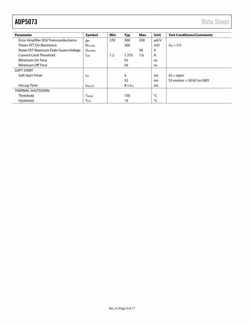
Parameter Symbol Min Typ Max Unit Test Conditions/Comments Error Amplifier (EA) Transconductance gM 270 300 330 µA/V Power FET On Resistance RDS (ON) 200 mΩ VIN = 5 V Power FET Maximum Drain Source Voltage VDS (MAX) 39 V Current-Limit Threshold ILIM 1.2 1.375 1.6 A Minimum On Time 55 ns Minimum Off Time 50 ns
SOFT START Soft Start Timer tSS 4 ms SS = open
32 ms SS resistor = 50 kΩ to GND Hiccup Time tHICCUP 8 × tSS ms
THERMAL SHUTDOWN Threshold TSHDN 150 °C Hysteresis THYS 15 °C

Data Sheet ADP5073
Rev. A | Page 5 of 17
ABSOLUTE MAXIMUM RATINGS Table 3. Parameter Rating PVIN, AVIN −0.3 V to +18 V SW PVIN − 40 V to PVIN + 0.3 V GND −0.3 V to +0.3 V VREG −0.3 V to lower of AVIN + 0.3 V or +6 V EN, FB, SYNC/FREQ, PWRGD −0.3 V to +6 V COMP, SLEW, SS, VREF −0.3 V to VREG + 0.3 V Operating Junction
Temperature Range −40°C to +125°C
Storage Temperature Range
−65°C to +150°C
Soldering Conditions JEDEC J-STD-020
Stresses at or above those listed under Absolute Maximum Ratings may cause permanent damage to the product. This is a stress rating only; functional operation of the product at these or any other conditions above those indicated in the operational section of this specification is not implied. Operation beyond the maximum operating conditions for extended periods may affect product reliability.
THERMAL RESISTANCE θJA and ΨJT are based on a 4-layer printed circuit board (PCB) (two signals and two power planes) with thermal vias connecting the exposed pad to a ground plane as recommended in the Layout Considerations section. θJC is measured at the top of the package and is independent of the PCB. The ΨJT value is more appropriate for calculating junction to case temperature in the application.
Table 4. Thermal Resistance Package Type θJA θJC ΨJT Unit 16-Lead LFCSP 75.01 55.79 0.95 °C/W
ESD CAUTION
ADP5073 Data Sheet
Rev. A | Page 6 of 17
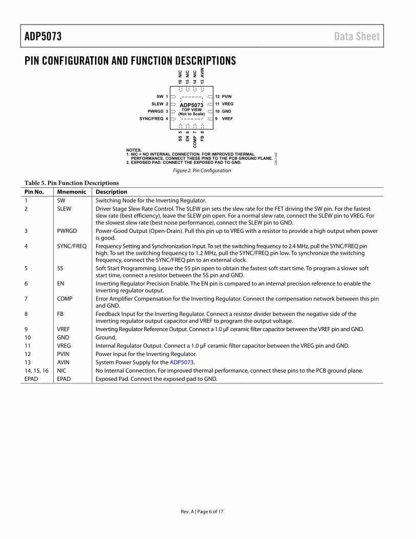
PIN CONFIGURATION AND FUNCTION DESCRIPTIONS
SW 1
SLEW 2
PWRGD 3
SYNC/FREQ 4
SS
5
1281
7-00
2
EN
6
CO
MP
7
FB
8
16
NIC
15
NIC
14
NIC
13
AV
IN
12 PVIN
11 VREG
10 GND
9 VREF
NOTES.1. NIC = NO INTERNAL CONNECTION. FOR IMPROVED THERMAL PERFORMANCE, CONNECT THESE PINS TO THE PCB GROUND PLANE.2. EXPOSED PAD. CONNECT THE EXPOSED PAD TO GND.
ADP5073TOP VIEW
(Not to Scale)
Figure 2. Pin Configuration
Table 5. Pin Function Descriptions Pin No. Mnemonic Description 1 SW Switching Node for the Inverting Regulator. 2 SLEW Driver Stage Slew Rate Control. The SLEW pin sets the slew rate for the FET driving the SW pin. For the fastest
slew rate (best efficiency), leave the SLEW pin open. For a normal slew rate, connect the SLEW pin to VREG. For the slowest slew rate (best noise performance), connect the SLEW pin to GND.
3 PWRGD Power-Good Output (Open-Drain). Pull this pin up to VREG with a resistor to provide a high output when power is good.
4 SYNC/FREQ Frequency Setting and Synchronization Input. To set the switching frequency to 2.4 MHz, pull the SYNC/FREQ pin high. To set the switching frequency to 1.2 MHz, pull the SYNC/FREQ pin low. To synchronize the switching frequency, connect the SYNC/FREQ pin to an external clock.
5 SS Soft Start Programming. Leave the SS pin open to obtain the fastest soft start time. To program a slower soft start time, connect a resistor between the SS pin and GND.
6 EN Inverting Regulator Precision Enable. The EN pin is compared to an internal precision reference to enable the inverting regulator output.
7 COMP Error Amplifier Compensation for the Inverting Regulator. Connect the compensation network between this pin and GND.
8 FB Feedback Input for the Inverting Regulator. Connect a resistor divider between the negative side of the inverting regulator output capacitor and VREF to program the output voltage.
9 VREF Inverting Regulator Reference Output. Connect a 1.0 μF ceramic filter capacitor between the VREF pin and GND. 10 GND Ground.11 VREG Internal Regulator Output. Connect a 1.0 μF ceramic filter capacitor between the VREG pin and GND. 12 PVIN Power Input for the Inverting Regulator. 13 AVIN System Power Supply for the ADP5073. 14, 15, 16 NIC No Internal Connection. For improved thermal performance, connect these pins to the PCB ground plane. EPAD EPAD Exposed Pad. Connect the exposed pad to GND.

Data Sheet ADP5073
Rev. A | Page 7 of 17
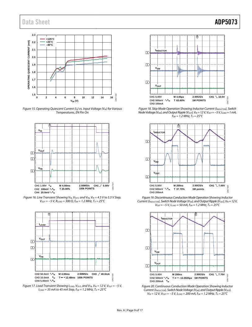
TYPICAL PERFORMANCE CHARACTERISTICS Typical performance characteristics are generated using the standard bill of materials for each input/output combination listed in Table 9.
1281
7-00
3
I OU
T (M
AX)
(mA
)
VOUT (V)
0
100
200
300
400
500
600
700
800
–40 –35 –30 –25 –20 –15 –10 –5 0
VIN = 3.3V, L = 5.6µHVIN = 3.3V, L = 6.8µHVIN = 5V, L = 6.8µHVIN = 5V, L = 10µHVIN = 12V, L = 15µHVIN = 12V, L = 22µHVIN = 15V, L = 15µH
Figure 3. Maximum Output Current, fSW = 1.2 MHz, TA = 25°C, Based on Target of 70% ILIM (MIN)
1281
7-00
4
I OU
T (M
AX)
(mA
)
VOUT (V)
0
100
200
300
400
500
600
–35 –30 –25 –20 –15 –10 –5 0
VIN = 3.3V, L = 2.2µHVIN = 3.3V, L = 3.3µHVIN = 5V, L = 3.3µHVIN = 5V, L = 5.6µHVIN = 12V, L = 6.8µHVIN = 12V, L = 10µHVIN = 15V, L = 6.8µH
Figure 4. Maximum Output Current, fSW = 2.4 MHz, TA = 25°C, Based on Target of 70% ILIM (MIN)
1281
7-00
5
EFFI
CIE
NC
Y (%
)
IOUT (A)
0
10
20
30
40
50
60
70
80
0.001 0.01 0.1 1 10
VIN = 12V, 1.2MHzVIN = 12V, 2.4MHz
Figure 5. Efficiency vs. Current Load (IOUT), VIN = 12 V, VOUT = −2.5 V, TA = 25°C
1281
7-00
6
EFFI
CIE
NC
Y (%
)
IOUT (A)
0
10
20
30
40
50
60
70
80
90
0.001 0.01 0.1 1
VIN = 12V, 1.2MHzVIN = 12V, 2.4MHz
Figure 6. Efficiency vs. Current Load (IOUT), VIN = 12 V, VOUT = −5 V, TA = 25°C
1281
7-00
7
EFFI
CIE
NC
Y (%
)
IOUT (A)
0
10
20
30
40
50
60
70
80
90
0.001 0.01 0.1 1
VIN = 12V, 1.2MHzVIN = 12V, 2.4MHzVIN = 5V, 1.2MHzVIN = 5V, 2.4MHz
Figure 7. Efficiency vs. Current Load (IOUT), VIN = 12 V and 5 V, VOUT = −15 V, TA = 25°C
1281
7-00
8
EFFI
CIE
NC
Y (%
)
IOUT (A)
0
10
20
30
40
50
60
70
80
90
0.001 0.01 0.1 1
VIN = 5V, 1.2MHzVIN = 5V, 2.4MHz
Figure 8. Efficiency vs. Current Load (IOUT), VIN = 5 V, VOUT = −30 V, TA = 25°C

ADP5073 Data Sheet
Rev. A | Page 8 of 17
1281
7-01
0
EFFI
CIE
NC
Y (%
)
IOUT (A)
0
10
20
30
40
50
60
70
80
90
0.001 0.01 0.1 1
–40°C+25°C+125°C
Figure 9. Efficiency vs. Current Load (IOUT) for Various Temperatures, VIN = 5 V, VOUT = −15 V, fSW = 1.2 MHz
1281
7-03
0
VAR
IATI
ON
IN V
REF
(VFB
) (%
)
VIN (V)
–0.50
–0.30
–0.10
0.10
0.30
0.50
0 2 4 6 8 10 12 14
Figure 10. Line Regulation, VOUT = −5 V, fSW = 1.2 MHz, 15 mA Load, TA = 25°C (Skip Mode Not Shown)
1281
7-03
1
VAR
IATI
ON
IN V
REF
(VFB
) (%
)
LOAD (A)
–0.50
–0.30
–0.10
0.10
0.30
0.50
0 0.1 0.2 0.3 0.4 0.5 0.6 0.7 0.8 0.9 1
1.2 MHz2.4 MHz
Figure 11. Load Regulation, VIN = 12 V, VOUT = −5 V, fSW = 1.2 MHz, TA = 25°C (Skip Mode Not Shown)
0 4 8 12 162 6 10 14
OSC
ILLA
TOR
FREQ
UEN
CY
(MH
z)
VIN (V)
TA = –40°CTA = +25°CTA = +125°C
1281
7-01
32.24
2.29
2.34
2.39
2.44
2.49
2.54
Figure 12. Oscillator Frequency vs. Input Voltage (VIN) for Various Temperatures, SYNC/FREQ Pin = High
1281
7-01
4
0 4 8 12 162 6 10 14
OSC
ILLA
TOR
FREQ
UEN
CY(M
Hz)
VIN (V)
TA = –40°CTA = +25°CTA = +125°C
1.13
1.27
1.25
1.23
1.21
1.19
1.17
1.15
Figure 13. Oscillator Frequency vs. Input Voltage (VIN) for Various Temperatures, SYNC/FREQ Pin = Low
1281
7-01
5
SHU
TDO
WN
QU
IESC
ENT
CU
RR
ENT
(µA
)
VIN (V)
0
2
4
6
8
10
12
14
16
18
0 2 4 6 8 10 12 14 16
+80°C+25°C–40°C
Figure 14. Shutdown Quiescent Current (ISHDN) vs. Input Voltage (VIN) for Various Temperatures, EN Pin Below Shutdown Threshold
Data Sheet ADP5073
Rev. A | Page 9 of 17
1281
7-01
6
OPE
RA
TIN
G Q
UIE
SCEN
T C
UR
REN
T (m
A)
VIN (V)
1.5
1.6
1.7
1.8
1.9
2.0
2.1
2.2
2.3
0 2 4 6 8 10 12 14 16
+125°C+25°C–40°C
Figure 15. Operating Quiescent Current (IQ) vs. Input Voltage (VIN) for Various Temperatures, EN Pin On
CH1 5.00V
2
1
4
1281
7-01
7
CH2 100mVCH4 20.0mV
CH1 1.00V 2.50MS/s100k POINTS
BWBWBW
M 4.00msT 20.00%
VOUT
VFB
VIN
Figure 16. Line Transient Showing VIN, VOUT, and VFB, VIN = 4.5 V to 5.5 V Step, VOUT = −5 V, RLOAD = 300 Ω, fSW = 1.2 MHz, TA = 25°C
CH3 40.0mA
2
3
4
1281
7-01
8
CH3 10.0mACH4 5.00mV
CH2 50.0mV 2.50MS/s100k POINTSBW
BW
BW
M 4.00msT 12.48ms
VOUT
VFB
ILOAD
Figure 17. Load Transient Showing ILOAD, VOUT, and VFB, VIN = 12 V, VOUT = −5 V, ILOAD = 35 mA to 45 mA Step, fSW = 1.2 MHz, TA = 25°C
CH1 10.0V
1
3
2
1281
7-01
9
CH2 500mVCH3 100mA
CH1 5.00V 2.50GS/s1M POINTSBW
M 4.00µsT 63.60%
VSW
VOUT
IINDUCTOR
Figure 18. Skip Mode Operation Showing Inductor Current (IINDUCTOR), Switch Node Voltage (VSW), and Output Ripple (VOUT), VIN = 12 V, VOUT = −5 V, ILOAD = 1 mA,
fSW = 1.2 MHz, TA = 25°C
VSW
VOUT
IINDUCTOR
CH1 7.00V
1
3
2
1281
7-02
0
CH2 500mVCH3 200mA
CH1 5.00V 2.50GS/s1M pointsBW
M 200nsT 37.70%
Figure 19. Discontinuous Conduction Mode Operation Showing Inductor Current (IINDUCTOR), Switch Node Voltage (VSW), and Output Ripple (VOUT), VIN = 12 V,
VOUT = −5 V, ILOAD = 50 mA, fSW = 1.2 MHz, TA = 25°C
CH1 7.70V
1
3
2
1281
7-02
1
CH2 500mVCH3 200mA
CH1 5.00V 2.50GS/s1M POINTSBW
BW
M 200ns
VSW
VOUT
IINDUCTOR
T –13.0020µs
Figure 20. Continuous Conduction Mode Operation Showing Inductor Current (IINDUCTOR), Switch Node Voltage (VSW), and Output Ripple (VOUT),
VIN = 12 V, VOUT = −5 V, ILOAD = 200 mA, fSW = 1.2 MHz, TA = 25°C

ADP5073 Data Sheet
Rev. A | Page 10 of 17
THEORY OF OPERATION VIN
CIN
HIGH VOLTAGEBAND GAP
SW
FB
INVERTERPWM CONTROL
PVIN
ERROR AMP
HIGH VOLTAGEREGULATOR
EN
AVIN VREG
CVREG
COMP
SLEW
SYNC/FREQ
SS GND
CURRENTSENSE
START-UPTIMERS
PLL
4µA
REF
CONTROL
OSCILLATOR
SLEW
EN
RFB
RFT
L1
D1
COUT
RSS (OPTIONAL)
THERMALSHUTDOWN
UVLO
OVP
VREFVREG
FB
REFERENCEGENERATOR REF_1.6V
REF_1.6V
REF
CVREF
RC
CC
POWERGOOD
REFPWRGD
VREG
RPG(OPTIONAL)
1281
7-02
3
Figure 21. Functional Block Diagram
PWM MODE The inverting regulator in the ADP5073 operates at a fixed fre-quency set by an internal oscillator. At the start of each oscillator cycle, the MOSFET switch turns on, applying a positive voltage across the inductor. The inductor current (IINDUCTOR) increases until the current sense signal crosses the peak inductor current threshold that turns off the MOSFET switch; this threshold is set by the error amplifier output. During the MOSFET off time, the inductor current declines through the external diode until the next oscillator clock pulse starts a new cycle. The ADP5073 regulates the output voltage by adjusting the peak inductor current threshold.
SKIP MODE During light load operation, the regulator can skip pulses to maintain output voltage regulation. Skipping pulses increases the device efficiency. The COMP voltage is monitored internally and when it falls below a threshold (due to the output voltage rising above the target during a switching cycle), the next switching cycle is skipped. This voltage is monitored on a cycle-by-cycle basis. During skip operation, the output ripple is increased and the ripple frequency varies. The choice of inductor defines the output current below which skip mode occurs.
UNDERVOLTAGE LOCKOUT (UVLO) The UVLO circuitry monitors the AVIN pin voltage level. If the input voltage drops below the VUVLO_FALLING threshold, the regulator turns off. After the AVIN pin voltage rises above the VUVLO_RISING threshold, the soft start period initiates, and the regulator is enabled.
OSCILLATOR AND SYNCHRONIZATION A phase-locked loop (PLL)-based oscillator generates the internal clock and offers a choice of two internally generated frequency options or external clock synchronization. The switching frequency is configured using the SYNC/FREQ pin options shown in Table 6.
For external synchronization, connect the SYNC/FREQ pin to a suitable clock source. The PLL locks to an input clock within the range specified by fSYNC.
Table 6. SYNC/FREQ Pin Options SYNC/FREQ Pin Switching Frequency High 2.4 MHz Low 1.2 MHz External Clock 1× clock frequency
INTERNAL REGULATORS The internal VREG regulator in the ADP5073 provides a stable power supply for the internal circuitry. The VREG supply provides a high signal for device configuration pins but must not be used to supply external circuitry.
The VREF regulator provides a reference voltage for the inverting regulator feedback network to ensure a positive feedback voltage on the FB pin. A current-limit circuit is included for both internal regulators to protect the circuit from accidental loading.
Data Sheet ADP5073
Rev. A | Page 11 of 17
PRECISION ENABLING The ADP5073 has an enable pin that features a precision enable circuit with an accurate reference voltage. This reference allows the ADP5073 to be sequenced easily from other supplies. It can also be used as a programmable UVLO input by using a resistor divider.
The enable pin has an internal pull-down resistor that defaults to off when the pin is floating. When the voltage at the enable pin is greater than the VTH_H reference level, the regulator is enabled.
SOFT START The regulator in the ADP5073 includes soft start circuitry that ramps the output voltage in a controlled manner during startup, thereby limiting the inrush current. The soft start time is internally set to the fastest rate when the SS pin is open.
Connecting a resistor between SS and ground allows the adjustment of the soft start delay.
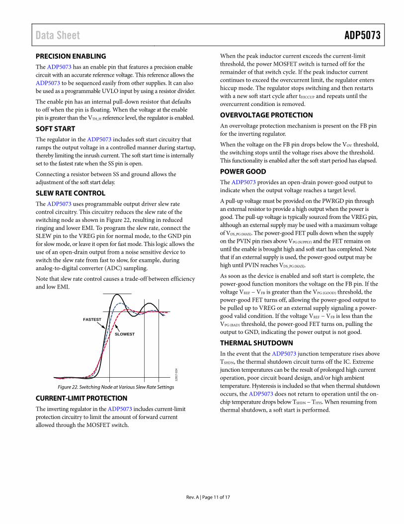
SLEW RATE CONTROL The ADP5073 uses programmable output driver slew rate control circuitry. This circuitry reduces the slew rate of the switching node as shown in Figure 22, resulting in reduced ringing and lower EMI. To program the slew rate, connect the SLEW pin to the VREG pin for normal mode, to the GND pin for slow mode, or leave it open for fast mode. This logic allows the use of an open-drain output from a noise sensitive device to switch the slew rate from fast to slow, for example, during analog-to-digital converter (ADC) sampling.
Note that slew rate control causes a trade-off between efficiency and low EMI.
FASTEST
SLOWEST
1281
7-02
4
Figure 22. Switching Node at Various Slew Rate Settings
CURRENT-LIMIT PROTECTION The inverting regulator in the ADP5073 includes current-limit protection circuitry to limit the amount of forward current allowed through the MOSFET switch.
When the peak inductor current exceeds the current-limit threshold, the power MOSFET switch is turned off for the remainder of that switch cycle. If the peak inductor current continues to exceed the overcurrent limit, the regulator enters hiccup mode. The regulator stops switching and then restarts with a new soft start cycle after tHICCUP and repeats until the overcurrent condition is removed.
OVERVOLTAGE PROTECTION An overvoltage protection mechanism is present on the FB pin for the inverting regulator.
When the voltage on the FB pin drops below the VOV threshold, the switching stops until the voltage rises above the threshold. This functionality is enabled after the soft start period has elapsed.
POWER GOOD The ADP5073 provides an open-drain power-good output to indicate when the output voltage reaches a target level.
A pull-up voltage must be provided on the PWRGD pin through an external resistor to provide a high output when the power is good. The pull-up voltage is typically sourced from the VREG pin, although an external supply may be used with a maximum voltage of VDS_PG (MAX). The power-good FET pulls down when the supply on the PVIN pin rises above VPG (SUPPLY) and the FET remains on until the enable is brought high and soft start has completed. Note that if an external supply is used, the power-good output may be high until PVIN reaches VDS_PG (MAX).
As soon as the device is enabled and soft start is complete, the power-good function monitors the voltage on the FB pin. If the voltage VREF − VFB is greater than the VPG (GOOD) threshold, the power-good FET turns off, allowing the power-good output to be pulled up to VREG or an external supply signaling a power-good valid condition. If the voltage VREF − VFB is less than the VPG (BAD) threshold, the power-good FET turns on, pulling the output to GND, indicating the power output is not good.
THERMAL SHUTDOWN In the event that the ADP5073 junction temperature rises above TSHDN, the thermal shutdown circuit turns off the IC. Extreme junction temperatures can be the result of prolonged high current operation, poor circuit board design, and/or high ambient temperature. Hysteresis is included so that when thermal shutdown occurs, the ADP5073 does not return to operation until the on-chip temperature drops below TSHDN − THYS. When resuming from thermal shutdown, a soft start is performed.

ADP5073 Data Sheet
Rev. A | Page 12 of 17
APPLICATIONS INFORMATION ADIsimPOWER DESIGN TOOL The ADP5073 is supported by the ADIsimPower™ design tool set. ADIsimPower is a collection of tools that produce complete power designs optimized to a specific design goal. These tools allow the user to generate a full schematic, bill of materials, and calculate performance in minutes. ADIsimPower can optimize designs for cost, area, efficiency, and device count while taking into consideration the operating conditions and limitations of the IC and all real external components. The ADIsimPower tool can be found at www.analog.com/adisimpower, and the user can request an unpopulated board through the tool.
COMPONENT SELECTION Feedback Resistors
The ADP5073 provides an adjustable output voltage. An external resistor divider sets the output voltage, where the divider output must equal the feedback reference voltage, VFB. To limit the output voltage accuracy degradation due to feedback bias current, ensure that the current through the divider is at least 10 × IFB.
Set the negative output for the inverting regulator by
( )FBREFFB
FTFBOUT VV
RRVV −−=
where: VOUT is the negative output voltage. VFB is the FB reference voltage. RFT is the feedback resistor from VOUT to FB. RFB is the feedback resistor from FB to VREF. VREF is the VREF pin reference voltage.
Table 7 shows recommended values for common output voltages using standard resistor values.
Table 7. Recommended Feedback Resistor Values Desired Output Voltage (V) RFT (MΩ) RFB (kΩ)
Actual Output Voltage (V)
−1.8 0.332 102 −1.804 −3 0.475 100 −3.000 −3.3 0.523 102 −3.302 −4.2 0.715 115 −4.174 −5 1.15 158 −5.023 −9 1.62 133 −8.944 −12 1.15 71.5 −12.067 −13 2.8 162 −13.027 −15 2.32 118 −14.929 −18 2.67 113 −18.103 −20 2.94 113 −20.014 −24 3.16 102 −23.984 −30 4.12 107 −30.004 −35 5.11 115 −34.748
Output Capacitor
Higher output capacitor values reduce the output voltage ripple and improve load transient response. When choosing this value, it is also important to account for the loss of capacitance due to the output voltage dc bias.
Ceramic capacitors are manufactured with a variety of dielectrics, each with a different behavior over temperature and applied voltage. Capacitors must have a dielectric adequate to ensure the minimum capacitance over the necessary temperature range and dc bias conditions. X5R or X7R dielectrics with a voltage rating of 25 V or 50 V (depending on output) are recommended for best performance. Y5V and Z5U dielectrics are not recommended for use with any dc-to-dc converter because of their poor temperature and dc bias characteristics.
Calculate the worst case capacitance accounting for capacitor variation over temperature, component tolerance, and voltage using the following equation:
CEFFECTIVE = CNOMINAL × (1 − TEMPCO) × (1 − DCBIASCO) × (1 − Tolerance)
where: CEFFECTIVE is the effective capacitance at the operating voltage. CNOMINAL is the nominal data sheet capacitance. TEMPCO is the worst case capacitor temperature coefficient. DCBIASCO is the dc bias derating at the output voltage. Tolerance is the worst case component tolerance.
To guarantee the performance of the device, it is imperative that the effects of dc bias, temperature, and tolerances on the behavior of the capacitors be evaluated for each application.
Capacitors with lower effective series resistance (ESR) and effective series inductance (ESL) are preferred to minimize output voltage ripple.
Note that the use of large output capacitors may require a slower soft start to prevent current limit during startup. A 10 µF capacitor is suggested as a good balance between performance and size.
Input Capacitor
Higher value input capacitors help reduce the input voltage ripple and improve transient response.
To minimize supply noise, place the input capacitor as close as possible to the AVIN and PVIN pins. A low ESR capacitor is recommended.
For stability, the use of a good quality 10 µF ceramic capacitor with low dc bias effects is recommended. If the power pins are individually decoupled, it is recommended to use a minimum of a 5.6 µF capacitor on the PVIN pin and a 3.3 µF capacitor on the AVIN pin.

Data Sheet ADP5073
Rev. A | Page 13 of 17
VREG Capacitor
A 1.0 µF ceramic capacitor (CVREG) is required between the VREG pin and GND.
VREF Capacitor
A 1.0 µF ceramic capacitor (CVREF) is required between the VREF pin and GND.
Soft Start Resistor
A resistor (RSS) can be connected between the SS pin and the GND pin to increase the soft start time. The soft start time can be set using this resistor between 4 ms (268 kΩ) and 32 ms (50 kΩ). Leaving the SS pin open selects the fastest time of 4 ms. Figure 23 shows the behavior of this operation. Calculate the soft start time (tSS) using the following formula:
tSS = 38.4 × 10⁻³ − 1.28 × 10⁻⁷ × RSS (Ω)
where 50 kΩ ≤ RSS ≤ 268 kΩ.
SS PIN OPEN
SOFT STARTTIMER
SOFT STARTRESISTORR1R2
32ms
4ms
1281
7-02
5
Figure 23. Soft Start Behavior
Diodes
A Schottky diode with low junction capacitance is recommended for D1. At higher output voltages and especially at higher switching frequencies, the junction capacitance is a significant contributor to efficiency. Higher capacitance diodes also generate more switching noise. As a guide, a diode with less than 40 pF junction capacitance is preferred when the output voltage is in the range of −5 V to −37 V.
Inductor Selection
The inductor stores energy during the on time of the power switch, and transfers that energy to the output through the output rectifier during the off time. To balance the trade-offs between small inductor current ripple and efficiency, inductance values in the range of 1 µH to 22 µH are recommended. In general, lower inductance values have higher saturation current and lower series resistance for a given physical size. However, lower inductance results in a higher peak current that can lead to reduced efficiency and greater input and/or output ripple and noise. A peak-to-peak inductor ripple current close to 30% of the maximum dc current in the inductor typically yields an optimal compromise.
For the smallest solution size, inductors with a saturation current below ILIM may be used when the output current in the application is such that the inductor current stays below the saturated region.
For the inductor ripple current in continuous conduction mode (CCM) operation, the input (VIN) and output (VOUT) voltages determine the switch duty cycle (Duty) by the following equation:
+++
=DIODEOUTIN
DIODEOUT
VVVVV
Duty||
||
where VDIODE is the forward voltage drop of the Schottky diode (D1).
Determine the dc current in the inductor in CCM (IL1) using the following equation:
)1( DutyI
I OUTL1 −=
Using the duty cycle (Duty) and switching frequency (fSW), determine the on time (tON) using the following equation:
SWON f
Dutyt =
The inductor ripple current (∆IL1) in steady state is calculated by
L1tV
I ONINL1
×=∆
Solve for the inductance value (L1) using the following equation:
L1
ONIN
ItV
L1∆×
=
Assuming an inductor ripple current of 30% of the maximum dc current in the inductor results in
OUT
ONIN
IDutytV
L1×
−××=
3.0)1(
Ensure that the peak inductor current (the maximum input current plus half the inductor ripple current) is below the rated saturation current of the inductor. Likewise, ensure that the maximum rated rms current of the inductor is greater than the maximum dc input current to the regulator.
When operating the ADP5073 inverting regulator in CCM, for stable current mode operation, ensure that the selected inductance is equal to or greater than the minimum calculated inductance, LMIN, for the application parameters in the following equation:
−
−×=> 33.0
)1(27.0Duty
VLL1 INMIN (µH)
Table 9 suggests a series of inductors to use with the ADP5073 inverting regulator.

ADP5073 Data Sheet
Rev. A | Page 14 of 17
Loop Compensation
The ADP5073 uses external components to compensate the regulator loop, allowing the optimization of the loop dynamics for a given application. It is recommended to use the ADIsimPower tool to calculate compensation components.
The inverting converter, produces a right half plane zero in the regulation feedback loop. This feedback loop requires compensat-ing the regulator such that the crossover frequency occurs well below the frequency of the right half plane zero. The right half plane zero frequency is determined by the following equation:
DutyL1πDuty)(R
(RHP)f2
LOADZ ××
−=
21
where: fZ (RHP) is the right half plane zero frequency. RLOAD is the equivalent load resistance or the output voltage divided by the load current.
+++
=DIODEOUTIN
DIODEOUT
V||VVV||V
Duty
where VDIODE is the forward voltage drop of the Schottky diode (D1).
To stabilize the regulator, ensure that the regulator crossover frequency is less than or equal to one-tenth of the right half plane zero frequency.
The regulator loop gain is
OUTCSCOMPOUT
MOUTIN
IN
OUT
FBVL
ZGZ||R
GVV
V||V
VA
××
×××+
×=|)|2(
where: AVL is the regulator loop gain. VFB is the feedback regulation voltage. VOUT is the regulated negative output voltage. VIN is the input voltage. GM is the error amplifier transconductance gain. ROUT is the output impedance of the error amplifier and is 33 MΩ. ZCOMP is the impedance of the series RC network from COMP to GND. GCS is the current sense transconductance gain (the inductor current divided by the voltage at COMP), which is internally set by the ADP5073 and is 6.25 A/V. ZOUT is the impedance of the load in parallel with the output capacitor.
To determine the crossover frequency, it is important to note that, at that frequency, the compensation impedance (ZCOMP) is dominated by a resistor, RC, and the output impedance (ZOUT) is dominated by the impedance of the output capacitor (COUT).
Therefore, when solving for the crossover frequency, the equation (by definition of the crossover frequency) is simplified to
12
1|)|2(
=××
××
×××+
×=
OUTCCSC
MOUTIN
IN
OUT
FBVL
CfπGR
GVV
V||V
VA
where fC is the crossover frequency.
To solve for RC, use the following equation:
CSMINFB
OUTINOUTOUTCC GGVV
V(V||VCfπR
××××+××××
=|)|2(2
where GCS = 6.25 A/V.
Using typical values for VFB and GM results in
IN
OUTINOUTOUTCC V
VVVCfR
|)|2((||4188 ×+××××=
For better accuracy, it is recommended to use the value of output capacitance (COUT) that takes into account the capacitance reduction from dc bias in the calculation for RC.
After the compensation resistor is known, set the zero formed by CC and RC to one-fourth of the crossover frequency, or
CCC Rfπ
C××
=2
where CC is the compensation capacitor. ERROR
AMPLIFIER
REFgM
FBCOMP
RCCB
CC
1281
7-02
6
Figure 24. Compensation Components
The optional capacitor, CB, is chosen to cancel the zero introduced by the ESR of the output capacitor. For low ESR capacitors such as ceramic chip capacitors, CB can be omitted from the design.
Solve for CB as follows:
C
OUTB R
CESRC
×=
For optimal transient performance, RC and CC may need to be adjusted by observing the load transient response of the ADP5073. For most applications, RC is within the range of 1 kΩ to 200 kΩ, and CC is within the range of 1 nF to 68 nF.

Data Sheet ADP5073
Rev. A | Page 15 of 17
COMMON APPLICATIONS Table 8 and Table 9 list a number of common component selections for typical VIN and VOUT conditions. These have been bench tested and provide an off the shelf solution. To optimize components for an application, it is recommended to use the ADIsimPower tool set.
Figure 25 shows the schematic referenced by Table 8 and Table 9 with example component values for a +5 V input to a −15 V output. Table 8 shows the components common to all VIN and VOUT conditions.
Table 8. Recommended Common Components Selections Reference Value (µF) Part Number Manufacturer CIN 10 TMK316B7106KL-TD Taiyo Yuden CVREG 1 GRM188R71A105KA61D Murata CVREF 1 GRM188R71A105KA61D Murata
RC240Ω
CC470nF
VIN+12V
L14.7µH
D1DFLS240L
RFB158kΩ
CVREF1µF
CVREG1µF
RFT1.15MΩ
ADP5073
COMP
VREG
SS
EN
GND
AVIN
PVIN
SLEW
SYNC/FREQ
FB
SW
VREF
VOUT–5V
COUT10µF
ONOFF
PWRGDPWRGD
CIN10µF
RPG1MΩ
1281
7-02
7
Figure 25. Typical +12 V Input to −5 V Output, 1.2 MHz Application
Table 9. Recommended Inverting Regulator Components VIN (V)
VOUT (V)
Freq. (MHz)
L1 (µH) L1, Coilcraft®
COUT (µF) COUT, Murata
D1, Diodes, Inc.
RFT (MΩ)
RFB (kΩ)
CC (nF)
RC (kΩ)
3.3 −2.5 1.2 4.7 XAL4030-472ME_ 10 GRM32ER71H106KA12L DFLS240L 0.432 107 150 1 3.3 −2.5 2.4 2.2 XAL4020-222ME_ 10 GRM32ER71H106KA12L DFLS240L 0.432 107 33 2.2 3.3 −3.3 1.2 4.7 XAL4030-472ME 10 GRM32ER71H106KA12L DFLS240L 0.532 102 68 2 3.3 −3.3 2.4 2.2 XAL4020-222ME_ 10 GRM32ER71H106KA12L DFLS240L 0.532 102 15 4.3 3.3 −5 1.2 4.7 XAL4030-472ME 10 GRM32ER71H106KA12L DFLS240L 1.15 158 22 4.7 3.3 −5 2.4 3.3 XAL4030-332ME_ 10 GRM32ER71H106KA12L DFLS240L 1.15 158 12 6.8 5 −5 1.2 6.8 XAL4030-682ME_ 10 GRM32ER71H106KA12L DFLS240L 1.15 158 47 3 5 −5 2.4 3.3 XAL4030-332ME_ 10 GRM32ER71H106KA12L DFLS240L 1.15 158 10 6.8 5 −15 1.2 10 XAL4040-103ME_ 10 GRM32ER71H106KA12L DFLS240 2.32 118 6.8 20 5 −15 2.4 5.6 LPS5030-562MR_ 10 GRM32ER71H106KA12L DFLS240 2.32 118 2.2 36 5 −30 1.2 10 XAL4040-103ME_ 10 GRM32ER71H106KA12L DFLS240 4.12 107 1.5 91 5 −30 2.4 10 XAL4040-103ME_ 10 GRM32ER71H106KA12L DFLS240 4.12 107 1 91 12 −2.5 1.2 6.8 XAL4030-682ME_ 10 GRM32ER71H106KA12L DFLS240L 0.432 107 220 0.68 12 −2.5 2.4 3.3 XAL4030-332ME_ 10 GRM32ER71H106KA12L DFLS240L 0.432 107 47 1.3 12 −5 1.2 10 XAL4040-103ME_ 10 GRM32ER71H106KA12L DFLS240L 1.15 158 68 2 12 −5 2.4 5.6 LPS5030-562MR_ 10 GRM32ER71H106KA12L DFLS240L 1.15 158 20 3.3 12 −15 1.2 22 XAL5050-223ME_ 10 GRM32ER71H106KA12L DFLS240 2.32 118 22 9 12 −15 2.4 10 XAL4040-103ME_ 10 GRM32ER71H106KA12L DFLS240 2.32 118 3.3 20

ADP5073 Data Sheet
Rev. A | Page 16 of 17
LAYOUT CONSIDERATIONS PCB layout is important for all switching regulators but is particularly important for regulators with high switching frequencies. To achieve high efficiency, good regulation, good stability, and low noise, a well designed PCB layout is required. Follow these guidelines when designing PCBs:
Keep the input bypass capacitor, CIN, close to the PVIN pin and the AVIN pin. Route each of these pins individually tothe pad of this capacitor to minimize noise coupling between the power inputs, rather than connecting the two pins at the device. A separate capacitor can be used on the AVIN pinfor the best noise performance.
Keep the high current paths as short as possible. These paths include the connections between CIN, L1, D1, COUT, andGND and their connections to the ADP5073.
Keep high current traces as short and wide as possible tominimize parasitic series inductance, which causes spikingand EMI.
Avoid routing high impedance traces near any node con-nected to the SW pin or near Inductor L1 to prevent radiated switching noise injection.
Place the feedback resistors as close to the FB pin as possible to prevent high frequency switching noise injection.
Route a trace to RFT directly from the COUT pad foroptimum output voltage sensing.
Place the compensation components as close as possible toCOMP. Do not share vias to the ground plane with the feedback resistors to avoid coupling high frequency noise into the sensitive COMP pin.
Place the CVREF and CVREG capacitors as close to theVREG and VREF pins as possible. Ensure that short tracesare used between VREF and RFB.
L1
D1
CIN
COUT
CC
RFT RFB
RC
CVREF
CVREG
U1
VOUT GND
18m
m
14mm
GND
VIN
1281
7-02
8
Figure 26. Suggested Layout for 18 mm × 14 mm, +12 V Input to −5 V Output Application (Dashed Line Is Connected on the Internal Layer of the PCB; Other Vias Connected to the Ground Plane;
SS, EN, PWRGD, SLEW, and SYNC/FREQ Connections Not Shown for Clarity and Are Typically Connected on an Internal Layer)

Data Sheet ADP5073
Rev. A | Page 17 of 17
OUTLINE DIMENSIONS
0.300.230.18
1.751.60 SQ1.45
3.103.00 SQ2.90
10.50BSC
BOTTOM VIEWTOP VIEW
16
58
9
12
13
4
0.500.400.30
0.05 MAX0.02 NOM
0.20 REF
0.20 MIN
COPLANARITY0.08
PIN 1INDICATOR
0.800.750.70
COMPLIANT TOJEDEC STANDARDS MO-220-WEED-6.PKG
-005
138
SEATINGPLANE
SIDE VIEW
EXPOSEDPAD
02-2
3-20
17-E
PIN 1INDICATOR AREA OPTIONS(SEE DETAIL A)
DETAIL A(JEDEC 95)
FOR PROPER CONNECTION OFTHE EXPOSED PAD, REFER TOTHE PIN CONFIGURATION ANDFUNCTION DESCRIPTIONSSECTION OF THIS DATA SHEET.
Figure 27. 16-Lead Lead Frame Chip Scale Package [LFCSP]
3 mm × 3 mm Body and 0.75 mm Package Height (CP-16-22)
Dimensions shown in millimeters
ORDERING GUIDE Model1 Temperature Range Package Description Package Option Branding Code ADP5073ACPZ-R7 −40°C to +125°C 16-Lead Lead Frame Chip Scale Package [LFCSP] CP-16-22 LR1 ADP5073CP-EVALZ Evaluation Board 1 Z = RoHS Compliant Part.
©2015–2017 Analog Devices, Inc. All rights reserved. Trademarks and registered trademarks are the property of their respective owners. D12817-0-10/17(A)