1 A Lithography-friendly Structured ASIC Design Approach By: Salman Goplani* Rajesh Garg # Sunil P...
25
1 A Lithography- A Lithography- friendly friendly Structured ASIC Structured ASIC Design Approach Design Approach By: By: Salman Goplani* Salman Goplani* Rajesh Garg Rajesh Garg # Sunil P Khatri Sunil P Khatri # Mosong Cheng Mosong Cheng # * National Instruments, Austin, TX 78759 National Instruments, Austin, TX 78759 # Department of ECE, Texas A&M University, Department of ECE, Texas A&M University, College Station, TX College Station, TX
-
date post
19-Dec-2015 -
Category
Documents
-
view
214 -
download
0
Transcript of 1 A Lithography-friendly Structured ASIC Design Approach By: Salman Goplani* Rajesh Garg # Sunil P...
1
A Lithography-A Lithography-friendly Structured friendly Structured
ASIC Design ASIC Design ApproachApproach
By:By:Salman Goplani*Salman Goplani*
Rajesh Garg Rajesh Garg ##
Sunil P Khatri Sunil P Khatri ##
Mosong Cheng Mosong Cheng ##
**National Instruments, Austin, TX 78759National Instruments, Austin, TX 78759## Department of ECE, Texas A&M University, Department of ECE, Texas A&M University,
College Station, TXCollege Station, TX

2
OutlineOutline
Motivation Motivation Mask costs increasingMask costs increasing Systematic process variations increasingSystematic process variations increasing
Previous WorkPrevious Work Our ApproachOur Approach
NAND2 based circuit implementation NAND2 based circuit implementation methodologymethodology
Experimental ResultsExperimental Results ConclusionsConclusions

3
Motivation – Mask CostsMotivation – Mask CostsProcess Process (microns)(microns)
2.02.0 0.80.8 0.0.66
0.30.355
0.20.255
0.10.188
0.10.133
0.10.1
Single Mask Cost Single Mask Cost ($K)($K)
1.51.5 1.51.5 2.52.5 4.54.5 7.57.5 1212 4040 6060
# of Masks# of Masks 1212 1212 1212 1616 2020 2626 3030 3434
Mask Set cost Mask Set cost ($K)($K)
1818 1818 3030 7272 150150 312312 10010000
20002000 A full set of A full set of
lithography masks can lithography masks can cost between $1-3M. cost between $1-3M.
Roughly 25% reduction Roughly 25% reduction in ASIC design starts in ASIC design starts in past 7 years. in past 7 years. [Sematech Annual [Sematech Annual Report 2002], [ A. Report 2002], [ A. Sangiovanni-Sangiovanni-Vincentelli “The Tides Vincentelli “The Tides of EDA”, keynote talk, of EDA”, keynote talk, DAC 2003].DAC 2003].
Need an approach in Need an approach in which different designs which different designs share a set of masksshare a set of masks

4
Motivation - VariationsMotivation - Variations Process variations can be classified asProcess variations can be classified as
Random variationsRandom variations Systematic variationsSystematic variations
Random variations are Random variations are unpredictableunpredictable Caused by random fluctuations such as number of Caused by random fluctuations such as number of
dopant atomsdopant atoms Systematic variations Systematic variations
PredictablePredictable variation trends across a chip variation trends across a chip Caused by spatial dependencies during device Caused by spatial dependencies during device
processingprocessing Chemical and mechanical polishing (CMP)Chemical and mechanical polishing (CMP) Optical proximity effects (OPE)Optical proximity effects (OPE)
Changes in poly shapes translates into Changes in poly shapes translates into channel length channel length variationsvariations
Impacts circuit performance Impacts circuit performance more severelymore severely compared to metal compared to metal variationsvariations

5
Motivation – Structured Motivation – Structured ASICsASICs
Standard cell based design approach Standard cell based design approach (ASIC)(ASIC) Severely affectedSeverely affected by OPEs due to lack of by OPEs due to lack of
regularity in designregularity in design Optical proximity correction (OPC) is Optical proximity correction (OPC) is
performed to deal with OPEsperformed to deal with OPEs OPC needs to be performed on all layers for OPC needs to be performed on all layers for
each new ASIC designeach new ASIC design Computationally Computationally expensiveexpensive process process
Need a circuit design approach thatNeed a circuit design approach that Allows us to Allows us to shareshare a majority of fabrication a majority of fabrication
masks across different designs masks across different designs Allows us to share the OPC computation for Allows us to share the OPC computation for
some layers, across different designssome layers, across different designs Our approach Our approach achieves these goalsachieves these goals

6
Previous WorkPrevious Work Jayakumar et. al. 2004 proposed a Jayakumar et. al. 2004 proposed a
structured ASIC approach using a network structured ASIC approach using a network of fixed (medium) sized PLAsof fixed (medium) sized PLAs Large delay (area) overhead of ~260% (~240%)Large delay (area) overhead of ~260% (~240%)
Gulati et. al. 2007 reported a pass Gulati et. al. 2007 reported a pass transistor logic (PTL) based structured transistor logic (PTL) based structured ASIC approachASIC approach Delay and area overheads are ~50% and Delay and area overheads are ~50% and
~240%~240%
Pillegi et. al. 2003 reported that FPGAs are Pillegi et. al. 2003 reported that FPGAs are typically ~25X slower than ASICstypically ~25X slower than ASICs
Our approach provides a structured ASIC Our approach provides a structured ASIC solution with small area (~10%) and delay solution with small area (~10%) and delay (~35%) overheads(~35%) overheads

7
Our SolutionOur Solution Use a Use a regular array of 2-input NANDregular array of 2-input NAND cells as the cells as the
underlying circuit structure, and customize only underlying circuit structure, and customize only METAL and VIA masksMETAL and VIA masks NAND2 is functionally completeNAND2 is functionally complete Stock such arrays pre-processed until metallization Stock such arrays pre-processed until metallization
stepstep Or, use previously generated masks for all other layers Or, use previously generated masks for all other layers
and use new masks for only METAL, VIA layersand use new masks for only METAL, VIA layers To create an ASIC for a given design – To create an ASIC for a given design –
technology-map this design to the smallest technology-map this design to the smallest available NAND2 array available NAND2 array Only METAL and VIA masks require changesOnly METAL and VIA masks require changes Easier to fix bugs, since only METAL and VIA masks Easier to fix bugs, since only METAL and VIA masks
changechange Optimize poly layer mask for maximum yieldOptimize poly layer mask for maximum yield
Perform aggressive OPC on the poly layerPerform aggressive OPC on the poly layer Required to be done only Required to be done only onceonce Beneficial since performance highly sensitive to Beneficial since performance highly sensitive to
channel length variationschannel length variations

8
NAND2 Cell ArrayNAND2 Cell Array
NAND2 cells are placed NAND2 cells are placed
to create rectangularto create rectangular
array of cellsarray of cells
Some space is left betweenSome space is left between
two rows of NAND2 cellstwo rows of NAND2 cells Used for routingUsed for routing
9
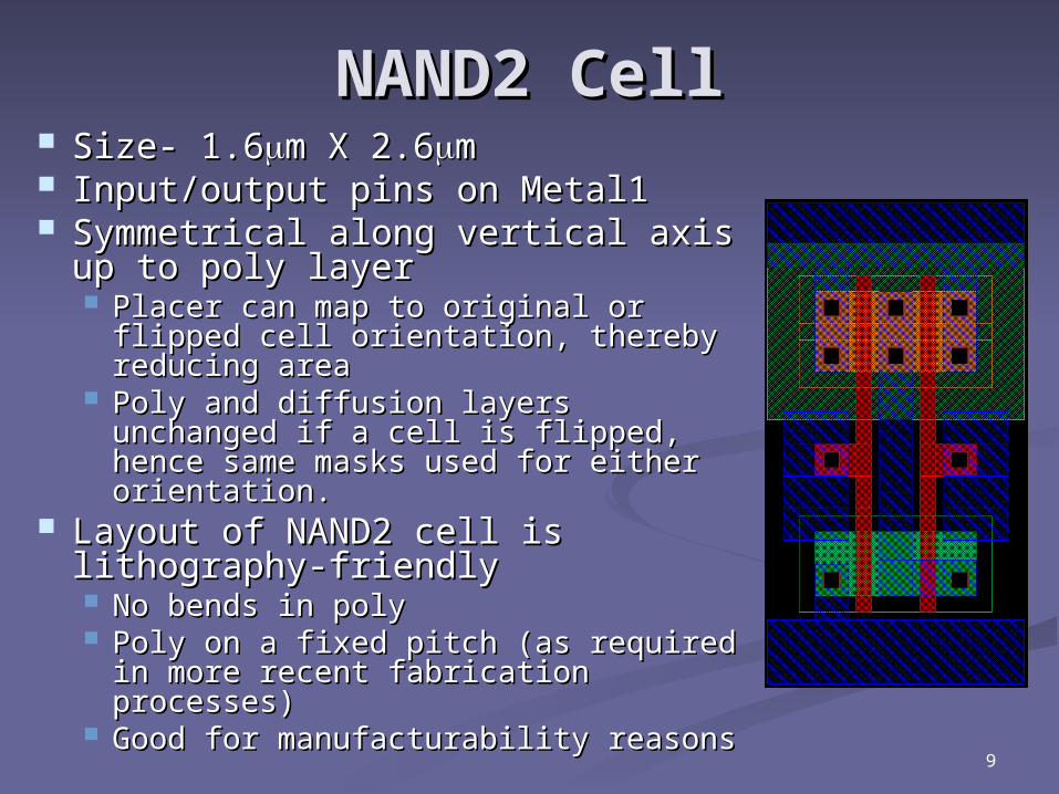
NAND2 CellNAND2 Cell Size- 1.6Size- 1.6m X 2.6m X 2.6mm Input/output pins on Metal1Input/output pins on Metal1 Symmetrical along vertical axis Symmetrical along vertical axis
up to poly layer up to poly layer Placer can map to original or Placer can map to original or
flipped cell orientation, thereby flipped cell orientation, thereby reducing areareducing area
Poly and diffusion layers unchanged Poly and diffusion layers unchanged if a cell is flipped, hence same if a cell is flipped, hence same masks used for either orientation.masks used for either orientation.
Layout of NAND2 cell is Layout of NAND2 cell is lithography-friendlylithography-friendly No bends in polyNo bends in poly Poly on a fixed pitch (as required in Poly on a fixed pitch (as required in
more recent fabrication processes)more recent fabrication processes) Good for manufacturability reasonsGood for manufacturability reasons

10
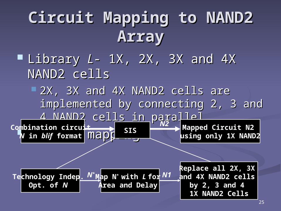
Circuit Mapping to NAND2 Circuit Mapping to NAND2 ArrayArray
Library Library L L consists of 1X, 2X, 3X and consists of 1X, 2X, 3X and 4X NAND2 cells4X NAND2 cells 2X, 3X and 4X NAND2 cells are 2X, 3X and 4X NAND2 cells are
implemented by connecting 2, 3 and 4 implemented by connecting 2, 3 and 4 NAND2 cells in parallelNAND2 cells in parallel
Combination circuit N in blif format
Place N2 using QPLACE -SEDSM and Route using
WROUTE
Technology indep. opt. of N
Map N* with L for area or delay
N*
N1
Replace all 2X, 3X or 4X NAND2 cells in N1 by 2, 3 or 4
1X NAND2 cells
N2

11
Characterization of NAND2 Characterization of NAND2 ArrayArray
DelayDelay ( (DD) is obtained using the ) is obtained using the sensesense package in package in SISSIS Sense reports the largest sensitizeable delay of the Sense reports the largest sensitizeable delay of the
circuit (excludes any false paths)circuit (excludes any false paths) We use gate netlist We use gate netlist N1N1 with 1X, 2X, 3X and 4X NAND2 with 1X, 2X, 3X and 4X NAND2
Power -Power - dynamic power of a circuit is dynamic power of a circuit is ff (= 1/ (= 1/DD) is the operating frequency of circuit ) is the operating frequency of circuit CCeffeff is the total switching capacitance is the total switching capacitance
where: where: CCkk is the capacitance of the node is the capacitance of the node kk
is the probability of transition of the node is the probability of transition of the node kk
fVDDCeff 2
2Nk
kxitkeff pCC
kxitp
12
Characterization of NAND2 Characterization of NAND2 ArrayArray
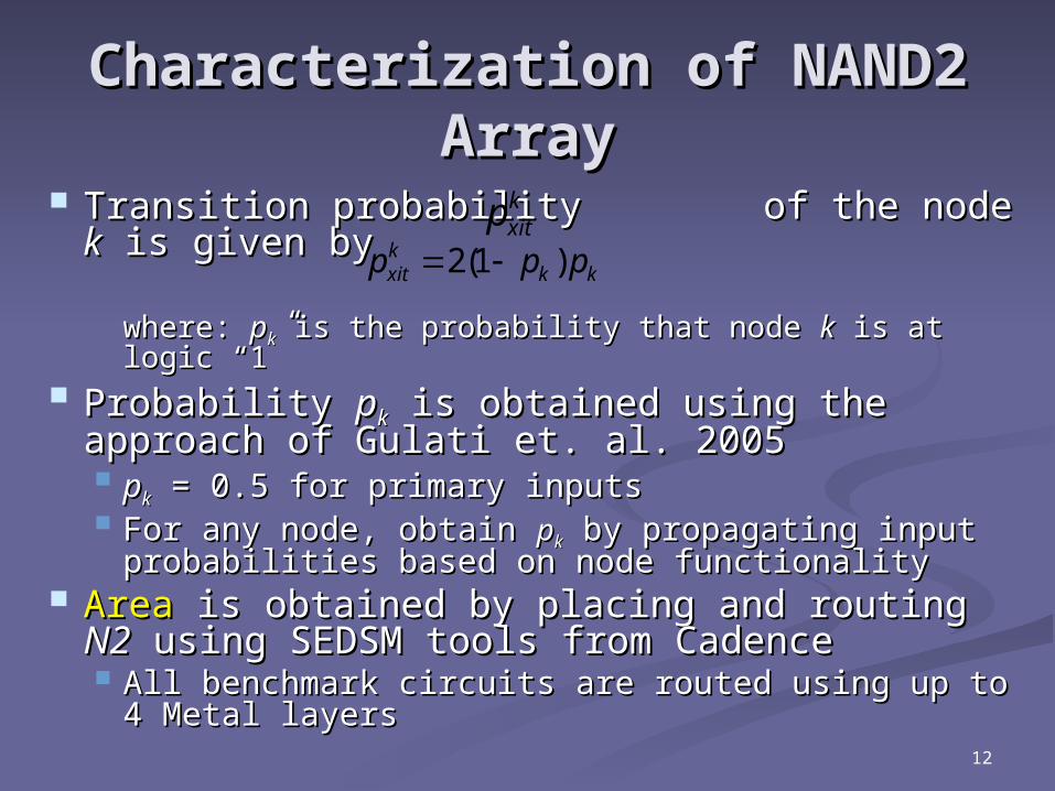
Transition probability of the node Transition probability of the node kk is is given bygiven by
where: where: ppkk is the probability that node is the probability that node kk is at is at logic “1”logic “1”
Probability Probability ppkk is obtained using the approach of is obtained using the approach of Gulati et. al. 2005Gulati et. al. 2005 ppkk = 0.5 for primary inputs = 0.5 for primary inputs For any node, obtain For any node, obtain ppkk by propagating input by propagating input
probabilities based on node functionalityprobabilities based on node functionality AreaArea is obtained by placing and routing is obtained by placing and routing N2N2
using SEDSM tools from Cadenceusing SEDSM tools from Cadence All benchmark circuits are routed using up to 4 All benchmark circuits are routed using up to 4
Metal layersMetal layers
kxitp
kkkxit ppp )1(2
13
Characterization of NAND2 Characterization of NAND2 ArrayArray
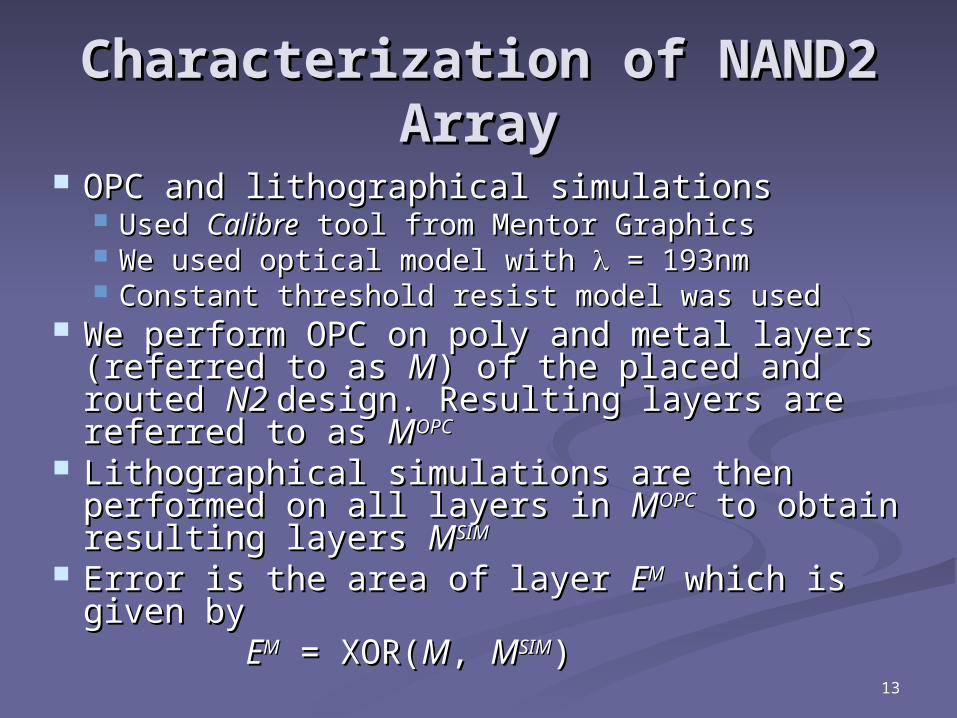
OPC and lithographical simulationsOPC and lithographical simulations Used Used CalibreCalibre tool from Mentor Graphics tool from Mentor Graphics We used optical model with We used optical model with = 193nm = 193nm Constant threshold resist model was usedConstant threshold resist model was used
We perform OPC on poly and metal layers We perform OPC on poly and metal layers (referred to as (referred to as MM) of the placed and routed ) of the placed and routed N2 N2 design. Resulting layers are referred to design. Resulting layers are referred to as as MMOPCOPC
Lithographical simulations are then Lithographical simulations are then performed on all layers in performed on all layers in MMOPCOPC to obtain to obtain resulting layers resulting layers MMSIMSIM
Error is the area of layer Error is the area of layer EEMM which is given which is given by by
EEMM = XOR( = XOR(MM, , MMSIMSIM))

14
Experimental ResultsExperimental Results Designed NAND2 cells library Designed NAND2 cells library LL using 100 using 100
BPTM with VDD = 1.2VBPTM with VDD = 1.2V Also implemented standard cell library Also implemented standard cell library LLSTDSTD
L L contains 1X, 2X, 3X and 4X NAND2 cellscontains 1X, 2X, 3X and 4X NAND2 cells LLSTD STD consists of INV and NAND, NOR, AND consists of INV and NAND, NOR, AND
& OR gates (with 2 and 3 inputs)& OR gates (with 2 and 3 inputs) Implemented several ISCAS and MCNC Implemented several ISCAS and MCNC
benchmark circuits using our approach and benchmark circuits using our approach and ASIC approachASIC approach
We mapped these designs for both area and We mapped these designs for both area and delay optimality delay optimality
15
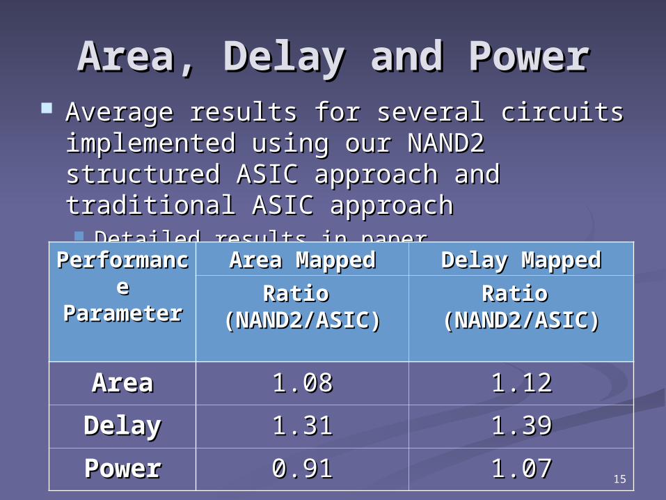
Area, Delay and PowerArea, Delay and Power Average results for several circuits Average results for several circuits
implemented using our NAND2 structured implemented using our NAND2 structured ASIC approach and traditional ASIC ASIC approach and traditional ASIC approachapproach Detailed results in paperDetailed results in paper
PerformanPerformance ce
ParameterParameter
Area MappedArea Mapped Delay MappedDelay Mapped
Ratio Ratio (NAND2/ASIC)(NAND2/ASIC)
Ratio Ratio (NAND2/ASIC)(NAND2/ASIC)
AreaArea 1.081.08 1.121.12
DelayDelay 1.311.31 1.391.39
PowerPower 0.910.91 1.071.07

16
Lithography SimulationLithography Simulation Ratio of lithographical error for poly and Metal1-Ratio of lithographical error for poly and Metal1-
4 layers for both approaches4 layers for both approaches
Errors on poly and Metal1 for our approach is Errors on poly and Metal1 for our approach is lower lower than ASIC approachthan ASIC approach Poly error translates into channel length variationsPoly error translates into channel length variations Sheet resistivity of Metal1 is higher than Metal2-4Sheet resistivity of Metal1 is higher than Metal2-4 Wires in these layers is largely restricted to within the Wires in these layers is largely restricted to within the
cell alonecell alone Our approach uses more wiring on Metal2-4 due Our approach uses more wiring on Metal2-4 due
to an overall area increase, resulting in an to an overall area increase, resulting in an increase in error on these layersincrease in error on these layers
EEPP EEM1M1 EEM2M2 EEM3M3 EEM4M4
Area Area MappedMapped
0.930.93 0.760.76 1.121.12 1.001.00 1.091.09
Delay Delay MappedMapped
0.940.94 0.710.71 1.191.19 1.051.05 1.061.06

17
ConclusionsConclusions With increasing cost of masks and process variationsWith increasing cost of masks and process variations
Need to implement circuits using regular structuresNeed to implement circuits using regular structures We presented a new structured ASIC approachWe presented a new structured ASIC approach
Implements circuits using Implements circuits using regular array of 2-input NAND regular array of 2-input NAND gatesgates
Our approach has Our approach has small overheadssmall overheads compared to compared to standard cell (ASIC) based design approachstandard cell (ASIC) based design approach Area - 12%Area - 12% Delay - 40%Delay - 40% Power - 7%Power - 7%
Lithographical errors of our approach are Lithographical errors of our approach are lowerlower on on poly and Metal1 layers by 7% and 24% compared to poly and Metal1 layers by 7% and 24% compared to ASIC approachASIC approach Our approach is Our approach is lithography friendlylithography friendly

18
`̀ Thank You!!Thank You!!

19
Backup SlidesBackup Slides

20
AREAAREA

21
DelayDelay
22
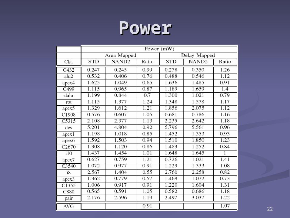
PowerPower

23
Lithographical ErrorLithographical Error

24
Implementing Sequential Implementing Sequential CircuitsCircuits
Flip Flop can be implemented using Flip Flop can be implemented using NAND2 gates as shownNAND2 gates as shown
25
Circuit Mapping to NAND2 Circuit Mapping to NAND2 ArrayArray
Library Library LL- 1X, 2X, 3X and 4X NAND2 - 1X, 2X, 3X and 4X NAND2 cellscells 2X, 3X and 4X NAND2 cells are 2X, 3X and 4X NAND2 cells are
implemented by connecting 2, 3 and 4 implemented by connecting 2, 3 and 4 NAND2 cells in parallelNAND2 cells in parallel
Circuit mapping Circuit mapping Combination circuit
N in blif format SIS Mapped Circuit N2
using only 1X NAND2
Technology Indep. Opt. of N
Map N* with L for Area and Delay
N* N1Replace all 2X, 3X
and 4X NAND2 cells by 2, 3 and 4
1X NAND2 Cells
N2