
0868 Final Report - University of British Columbiaqdg/publications/InternalReports/Ba… · ·...
74
FINAL REPORT FOR AN ULTRA-LOW NOISE HIGH GAIN PHOTODETECTOR FOR ATOM COUNTING Troy Barrie Greg Davis Project Sponsors: Dr. Kirk Madison, Dr. James Booth, Dr. Bruce Klappauf Applied Science 479 Engineering Physics University of British Columbia January 12 th , 2009 Project 0868
Transcript of 0868 Final Report - University of British Columbiaqdg/publications/InternalReports/Ba… · ·...

FINAL REPORT FOR AN ULTRA-LOW NOISE HIGH GAIN PHOTODETECTOR FOR ATOM COUNTING
Troy Barrie Greg Davis
Project Sponsors: Dr. Kirk Madison, Dr. James Booth, Dr. Bruce Klappauf
Applied Science 479 Engineering Physics
University of British Columbia January 12th, 2009
Project 0868

ii
Abstract
Magneto-optical traps (MOT) fluoresce at varying optical powers that are linearly
dependent on the number of atoms in the MOT. Detecting this fluorescence precisely and
consistently is important for studying the behaviour of MOTs, and for accurately
measuring relative atom counts in a MOT affected by a specific experimental event.
This project developed a photodetector specifically designed for such measurements for
Dr. Kirk Madison, Dr. James Booth, and Dr. Bruce Klappauf. The application requires a
photodetector with low noise, high gain, wide dynamic range, and good bandwidth.
Target specifications for the final product were: signal to noise ratio greater than 40 dB,
bandwidth greater than 10 kHz, selectable gain allowing accurate optical power
measurement from 10 nW to 10 µW, and use of a 1 cm2 photodiode.
The characterization results showed measurement capability covering the full specified
range, and minimum signal to noise ratio of 43 dB with typical signal to noise ratios
significantly higher (50 dB and greater). Four selectable gain stages of 100 MΩ, 50 MΩ,
10 MΩ, and 1 MΩ were included to allow precision measurement at all powers of
interest. The 100 MΩ gain stage is intended for DC high precision measurement with a
bandwidth less than 10 Hz but excellent noise performance (1 mV RMS noise), the 50
MΩ gain stage is intended for high sensitivity fast measurements and has a bandwidth of
2.5 kHz and noise of 8 mV RMS, the 10 MΩ gain stage has a bandwidth of 17 kHz and
noise of 5 mV RMS, and the 1 MΩ gain stage has a bandwidth of 60 kHz and noise of 1.8
mV RMS. The detector achieves the signal to noise ratio required at all powers, and
nearly achieves the bandwidth targets for the full power range, but at the lowest power of
interest, does not achieve the bandwidth and noise specification simultaneously. Each
detector employs a 1 cm2 FDS1010 photodiode for detection and includes an iris,
mounting cage, and shielding case.
Full calibration at 780 nm has been completed for the first detector, and less detailed
calibration has been completed for the other detectors.

iii
Table of Contents
Abstract ............................................................................................................................... ii
1 Background ...................................................................................................................... 1
2 Discussion ........................................................................................................................ 3
2.1 Objectives ................................................................................................................. 3 Electrical Specifications .............................................................................................. 3 Mechanical Specifications .......................................................................................... 3
2.2 Theory ....................................................................................................................... 4 2.2.1 Transimpedance Amplifier ................................................................................ 4
2.3 Design Process .......................................................................................................... 8 2.3.1 Simple Transimpedance Amplifier .................................................................... 9
2.3.2 Two Stage Amplifier ........................................................................................ 10 2.3.3 Differential Amplifier ...................................................................................... 12 2.3.4 Bootstrapped Cascode ...................................................................................... 13 2.3.5 Passive Component Selection .......................................................................... 14 2.3.6 Housing Design ................................................................................................ 15
2.4 Measurement Procedure .......................................................................................... 17 2.4.1 Photodiode Responsivity vs. Position of Incident Light .................................. 18
2.4.2 Noise ................................................................................................................ 19 2.4.3 Frequency Response ........................................................................................ 19 2.4.4 Photodetector Power Calibration ..................................................................... 20 2.4.5 Problems and Limitations ................................................................................ 21
2.5 Results ..................................................................................................................... 22
2.5.1 Photodiode Responsivity vs. Position .............................................................. 23
2.5.2 First Iteration Simple Prototype ....................................................................... 23 2.5.3 First Iteration Two Stage Prototype ................................................................. 26 2.5.4 Differential Prototype ...................................................................................... 28 2.5.5 Second Design Iteration ................................................................................... 30 2.5.6 Final Design Selection ..................................................................................... 31 2.5.7 Final Circuit, 1 pF Feedback Capacitance ....................................................... 32
2.5.8 Final Photodetector .......................................................................................... 34 3 Conclusions .................................................................................................................... 42
4 Recommendations .......................................................................................................... 44 Appendix A: Prototype Schematics .................................................................................. 45 Appendix B: Final Schematic and PCB Layout ............................................................... 51 Appendix C: Laser Driver Board ...................................................................................... 53 Appendix D: Power Calibration Curves ........................................................................... 54 References ......................................................................................................................... 68

iv
List of Tables
Table 1 Simple prototype first iteration RMS noise, CF = 4.7 pF. ................................... 25
Table 2 Two stage prototype dark current output with -5 V bias on photodiode ............ 28
Table 3 Two stage prototype first iteration RMS noise, CF = 10 pF. ............................... 28
Table 4 Differential prototype RMS noise, CF = 4.7 pF .................................................. 30 Table 5 Simple prototype second iteration results, CF = 0 ............................................... 30
Table 6 Final circuit comparison of RMS noise levels, CF = 1 pF. ................................. 33
Table 7 Final circuit noise comparison with different feedback capacitors, OPA381. .... 34
Table 8 Final detector gain resistances, feedback capacitances, and switch positions .... 35
Table 9 Final detector bandwidth and noise summary. .................................................... 36
List of Figures
Figure 1 Basic operation of a MOT [9] ............................................................................... 1
Figure 2 Model of a photodiode ......................................................................................... 4 Figure 3 Transimpedance amplifier ................................................................................... 5 Figure 4 Transimpedance amplifier noise model. .............................................................. 6
Figure 5 Noise and signal gain in the transimpedance amplifier ....................................... 7
Figure 6 Two op amp single gain stage design ................................................................ 10
Figure 7 Gain curves of the two stage circuit .................................................................. 11
Figure 8 Differential design ............................................................................................. 13 Figure 9 Bootstrapped Cascode ....................................................................................... 14 Figure 10 Mechanical design drawing of detectors in the system. .................................. 16
Figure 11 Optical system used for characterization and calibration measurements. ....... 18
Figure 12 Simple prototype schematic and first iteration frequency response ................ 24
Figure 13 Two stage prototype schematic and first iteration frequency response ........... 27
Figure 14 Differential prototype schematic and frequency response .............................. 29
Figure 15 Final design basic schematic ........................................................................... 32
Figure 16 Final circuit frequency response, OPA380, CF = 1 pF. ................................... 33
Figure 17 Final detector frequency response ................................................................... 35
Figure 18 Power calibration curve for Detector 2, 780 nm, 1 MΩ gain. ......................... 37
Figure 19 Power calibration curve for Detector 2, 780 nm, 10 MΩ gain. ....................... 38
Figure 20 Power calibration curve for Detector 2, 780 nm, 50 MΩ gain. ....................... 39
Figure 21 Power calibration curve for Detector 2, 780 nm, 100 MΩ gain. ..................... 40
Figure 22 Simple prototype first iteration schematic. ...................................................... 45
Figure 23 Two stage prototype first iteration schematic. ................................................. 46
Figure 24 Differential prototype schematic. .................................................................... 47
Figure 25 Simple prototype second iteration schematic. ................................................. 48
Figure 26 Two stage prototype second iteration schematic. ............................................ 49
Figure 27 Bootstrapped cascode prototype schematic. .................................................... 50
Figure 28 Final circuit schematic. .................................................................................... 51 Figure 29 Final PCB layout ............................................................................................. 52 Figure 30 Laser driver schematic. .................................................................................... 53

v
Figure 31 Detector 1 Power Calibration Curves ............................................................... 55 Figure 32 Detector 3 Power Calibration Curves ............................................................... 57 Figure 33 Detector 4 Power Calibration Curves ............................................................... 59 Figure 34 Detector 5 Power Calibration Curves ............................................................... 61 Figure 35 Detector 6 Power Calibration Curves ............................................................... 63 Figure 36 Detector 7 Power Calibration Curves ............................................................... 65 Figure 37 Detector 8 Power Calibration Curves ............................................................... 67

1
1 Background
Electronic applications frequently require amplification of an input signal originating
from a sensor or actuator. Depending upon the application, the amplifier can be
optimized to maximize either bandwidth or signal to noise ratio (SNR). In many cases,
bandwidth and SNR come as a trade-off; an increase in bandwidth results in a decrease in
SNR, and vice versa. Thus, each amplifier must be tuned to fit the desired electrical
specifications for the particular end application.
For this project, fluorescent light from atoms in a magneto-optical trap (MOT) is
collected onto a photodiode. The optical power of the fluorescence typically ranges from
nanowatts to microwatts, leading to the requirement of a transimpedance amplifier to
amplify the photocurrent and convert it to an output voltage. A MOT is a laser cooling
device in which momentum imparted to atoms by photons from lasers is used to restrict
the movement of atoms. This effect, utilized in conjunction with a magnetic field, forces
all of the atoms in the MOT to become trapped in a small volume. The result is an atom
cloud cooled to a few hundred micro-Kelvins and confined by radiation pressure. When
the atoms decay from an excited state to a ground state, they emit photons, generating
fluorescence whose intensity can be measured to monitor the behaviour and quantity of
the atoms in the MOT. A simplified conceptual outline of a MOT is shown in Figure 1.
Figure 1 Basic operation of a MOT [9]
2
In order for the MOT to operate, the lasers used for atomic cooling must be tuned close to
an atomic absorption frequency (wavelength) specific to the type of atom being cooled
and trapped. For this project, lithium atoms and rubidium atoms are being trapped,
dictating the wavelengths – 671 nm and 780 nm, respectively – at which the photodiode
must be calibrated.
The desired transimpedance amplifier should linearly amplify currents ranging from
approximately 5 nA to 5 µA and convert them to voltages that a mathematical model will
interpret to determine the number of atoms within the atom-cloud. A prototype of such a
transimpedance amplifier was designed and built by a previous student [6]. This model
uses a simplistic design, intended as an early exploration into the concept, but lacks the
high performance and permanence that motivate the objectives of this project. The crux
of the problem is the trade-off between maximizing the SNR while maintaining a high
bandwidth, and ensuring the full range of potential input photocurrents can be accurately
measured. The gain for the existing model is achieved using a 10 MΩ resistor; this
converts a 10 nA input signal to a 10 mV output signal. Capacitors within the circuit
must balance the capacitance of the photodiode to minimize noise gain and ensure
stability, yet still allow for high frequency signals to be amplified. The complications of
the signal bandwidth/noise gain trade-off are explained further in Section 2.1.1.
The project was sponsored by Dr. Kirk Madison and Dr. Bruce Klappauf of UBC
Physics, and BCIT visiting scientist Dr. James Booth. Commercial solutions are
available, but due to the high cost of these products, the fact that multiple detectors are
required, and the specific requirements and narrow application demands of the project, a
significantly cheaper in-house design was a viable and more attractive solution. For
example, two suitable commercial products are the Newport 1931-C high performance
low power optical meter, which costs $2400, and the Thorlabs PDA50B amplified
photodetector, which costs $469 and lacks the large area photodiode desired for the
project. The initial breadboard prototype completed earlier is currently in use in the lab,
but the project sponsors require a higher performance, fully characterized, calibrated,
permanent solution.

3
2 Discussion
2.1 Objectives
The primary objective of the project was to build eight photodetectors for measuring
fluorescence from Rubidium and Lithium magneto-optical traps. The detectors also were
to be calibrated and integrated into the optical systems in which they will be used. To
achieve the necessary level of precision, sensitivity, and performance, electrical
specifications were defined for the photodetector circuits; to allow integration into optical
systems and provide integration versatility, mechanical specifications were defined for
the housing of the photodetectors.
Electrical Specifications
• Optical power detection range 10 nW-10 µW
• Minimum 40 dB Signal to Noise Ratio throughout detection range
• Large area photodiode (1 cm2)
• Able to connect to 5-pin standardized lab power input (+/-5V, +/-15V, GND)
• Output to standard BNC cable
• Minimum 10 kHz bandwidth
• Selectable gain
Mechanical Specifications
• Physically fit into the system (as small as possible)
• Include Thorlabs optical mount with rails and 1 inch diameter threaded hole
• Include iris
• Include one inch diameter optical bandpass filter
The calibration and characterization of the detectors was also an important objective.
Characterization includes establishing the frequency response and noise level of the
detector for each selectable gain stage. Calibration consists of defining the relationship
between the input optical power at the photodiode and the output voltage level.

4
2.2 Theory
To detect optical power using a photodiode, one must measure the current emitted by the
photodiode accurately. The simplest way to do this is to connect the photodiode to a
resistor, converting the photocurrent directly to an easily measurable voltage. This
achieves an extremely low noise specification (the only noise sources are the Johnson
noise of the load resistor and the shot noise of the photodiode), but there are two
problems with this circuit. First, the voltage across the load resistor appears across the
photodiode. Since most photodiodes’ responsivity is dependent on the voltage across the
diode, this results in non-linear output. The second, more critical problem results from
the capacitance of the photodiode itself. A photodiode can be modelled as a parallel
combination of a current source, a capacitor, and a resistor, as shown in Figure 2.
Figure 2 Model of a photodiode. The capacitance of the diode causes problems when trying to take fast measurements.
Because the full voltage swing of the signal appears also across the capacitor CD, the
interaction between the capacitance of the photodiode and the load resistor limit the
bandwidth of the signal. One way of solving this problem is to use a transimpedance
amplifier.
2.2.1 Transimpedance Amplifier
The simplest version of the transimpedance amplifier is shown in Figure 3.

5
Figure 3 Transimpedance amplifier. Forcing the cathode of the photodiode to virtual ground by connecting it to an op amp allows the frequency response of the transimpedance amplifier to be expanded by limiting the voltage swing across the diode capacitance.
The most important feature of the transimpedance amplifier is that it maintains the
cathode of the photodiode D1 at virtual ground because it is connected to the non-
inverting input of the operational amplifier U1. This means that the voltage swing of the
output signal across the feedback resistor RF no longer appears across the capacitance of
the photodiode CD in the model of Figure 2. As the photocurrent changes, U1 changes its
output to shift the voltage at the cathode of the photodiode back to ground. Thus, the
bandwidth limit imposed by the interaction between the load resistor RF and the
capacitance of the photodiode CD has been mitigated. The cost of this bandwidth
improvement is the added noise that results from the addition of an active component. A
model of the transimpedance amplifier and its noise sources is shown in Figure 4. ID, the
photocurrent, INS, the shot noise of the photocurrent, and IJ, the Johnson noise of RF, are
all treated the same way by the circuit, and thus can be modelled in parallel as shown.
The diode shunt resistance in the model of Figure 3 has been omitted because in practice,
for a Silicon photodiode this resistance is so large that it has no effect on the operation of
the circuit.

6
Figure 4 Transimpedance amplifier noise model. The shot noise NS, Johnson noise NJ of the gain resistor RF, and signal current ID are all treated the same by the amplifier. The voltage noise of the amplifier eN is amplified according to the closed loop gain of the op amp.
The amplifier voltage noise eN is amplified by the non-inverting closed loop gain of the
op amp. The loop gain AVcl is given by [12]
where ZF is the complex impedance of the combination of RF and CF, and AVol is the open
loop gain of the op amp. This noise gain has a pole at the RC frequency defined by the
interaction between CD and RF, resulting in the noise gain peaking phenomenon. This
noise gain levels off at the same place that the signal begins to roll off; that is, the zero in
the transfer function caused by the RC interaction of RF and CF. The noise gain does not
roll off until the bandwidth limit of the op amp is reached, before which it is amplified by
an amount proportional to CD/CF. Essentially, this noise gain peaking means that high
frequency amplifier noise dominates the total noise, and the larger the photodiode
capacitance, the larger the effect of the noise gain peaking. The noise gain and signal
gain of the transimpedance amplifier are shown in Figure 5.

7
Figure 5 Noise and signal gain in the transimpedance amplifier. The signal gain rolls off beginning at the RC corner frequency defined by the feedback resistance and capacitance. The noise gain defined by the closed loop op amp gain has a pole at the RC corner frequency defined by the feedback resistor interacting with the photodiode capacitance, causing the noise gain to rise until it hits a zero at the RC corner where the signal gain begins rolling off. Above this frequency, the noise gain is constant at a ratio defined by the ratio of the feedback capacitance and the diode capacitance until it is rolled off by the op amp open loop gain limit.
This noise amplification effect can result in poor signal to noise ratio, or in some cases
oscillation of the op amp. Careful op amp selection and PCB layout are critical for
getting the best performance possible for the application.
Examining Figure 5, it is clear that increasing the feedback capacitance will reduce the
effect of noise gain peaking by shifting the zero of the noise gain curve left by reducing
the corner frequency 1/2πRFCF, thus reducing the peak level of the noise gain. However,
this comes at the expense of also reducing the bandwidth of the amplifier. In the limit
that the feedback capacitance matches the diode capacitance, the noise gain effect is
completely eliminated and the shot noise and Johnson noise physical limit is reached, as
in the case of the simple load resistor current to voltage converter; however, the

8
bandwidth is also reduced to the same low level as the simple load resistor, so nothing
has been gained. The challenge, then, is to find an optimal circuit that will trade off
bandwidth and noise to achieve a level that meets the specifications of the specific
application.
A circuit based on the transimpedance amplifier described above consists of the final
design of the photodetector for this project.
2.3 Design Process
The primary challenge of designing an amplifier to meet the specifications set out in the
project objectives stemmed from the combination of reconciling the very high sensitivity
required with the extremely large area photodiode, which carries with it an obese
capacitance of over 300 pF [4] at a bias voltage of -5 V. Maintaining a good signal to
noise ratio and salvaging as much bandwidth as possible with such high amplification and
diode capacitance was the major obstacle.
In order to overcome the challenge, several possible circuits were designed, fabricated,
and tested. In the first stage of prototyping, three designs were prototyped: the simple
transimpedance amplifier described in Section 2.2.1, a two stage amplifier employing two
op amps in combination in a single gain stage, and a differential design intended to
optimize common mode rejection. After this, a second prototyping stage was undertaken,
which included second iteration designs of the simple and two stage designs with slight
modifications, and a new design based around a bootstrapped cascode. The prototype
boards were fabricated using the LPKF milling machine in the UBC Engineering Physics
Project Lab.
After all the circuits had been tested, the simple transimpedance amplifier was selected as
the final design based on the testing results. The circuit design was then tweaked, and a
final printed circuit board (PCB) layout was created to be professionally fabricated. The

9
housing for the circuit and PCB layout were designed together to meet the mechanical
specifications outlined in the project objectives.
2.3.1 Simple Transimpedance Amplifier
The first design was the basic transimpedance amplifier shown in Figure 3. The full
schematic of the first iteration of this design is included in Appendix A. The design
included power regulation and decoupling, as well as four selectable gain resistors
ranging from 10 kΩ to 10 MΩ.
Selection of the op amp in this design is crucial. The op amp should have very low input
noise, low input currents, and low offset voltage. The Texas Instruments OPA381 is
specifically designed for transimpedance amplifiers, and made a suitable selection [4]. A
second, very similar op amp with the identical pinout to the OPA381, the OPA380 [19],
was also tested in this circuit. The primary difference between the two op amps is the
gain bandwidth product (GBW): the OPA380 has a GBW of 90 MHz, while the OPA381
has a GBW of 18 MHz. In the case of this project, because the bandwidth of the signal is
limited not by the op amp gain bandwidth product, but by the roll off caused by the RC
interaction of the feedback resistor and capacitor, the wider bandwidth OPA380 is not
necessary. In fact, the OPA381 performs better, because its narrower bandwidth limits
the spectrum available for noise gain peaking, rolling off the noise gain curve earlier (see
Figure 5).
This circuit was also designed to include a variable bias voltage on the photodiode that
could be tuned with a potentiometer to range from 0 to -15 V. The bias voltage design
included a minor error, however, which was corrected in the second iteration of the
design. The design required a voltage buffer between the voltage divider used to set the
bias voltage and the photodiode itself, which was missing in the first iteration design.
Biasing the photodiode has two major effects: first, by applying a voltage across the
photodiode, the capacitance of the diode is reduced, reducing the effect of the noise gain
peaking; second, a voltage across the photodiode results in a photocurrent being emitted

10
even when there is no incident light; this current is called dark current. The second
iteration of the simple prototype also improved power supply regulation and decoupling,
and added individual feedback capacitors for each feedback resistor.
2.3.2 Two Stage Amplifier
In an effort to improve noise performance without sacrificing bandwidth, a second circuit
incorporating two op amps was designed. A simplified schematic is shown in Figure 6.
The full schematic is shown in Appendix A.
Figure 6 Two op amp single gain stage design [1]. The integrator like response of the internal feedback loop formed by C1 and R4 creates a modified open loop gain curve that limits the bandwidth available for noise gain without limiting the signal bandwidth.
In this case, the first op amp IC1 should be very low noise, while the second op amp IC2
can be used to effectively limit the open loop bandwidth of the overall amplification
scheme to something just above the signal bandwidth. This eliminates the problem of
noise gain peaking at frequencies above the maximum signal frequency without limiting
signal bandwidth, provided that the modified open loop gain remains above the RC
frequency of the feedback resistor and capacitor. To demonstrate this effect, one can
qualitatively describe what happens at different frequencies. At low frequency, C1 is
11
effectively an open circuit, and the open loop gain is the product of the gain of IC1 and
the gain of IC2. However, at high frequencies, C1 becomes a short, and the open loop
gain is limited by the gain affected by the internal feedback network of R3 and R4. By
keeping R3 larger than R4, high frequencies will be attenuated. With correct component
selection, this design can allow the full signal bandwidth to remain unaffected, while
shifting the amplifier bandwidth limit back to roll off the noise gain peaking earlier and
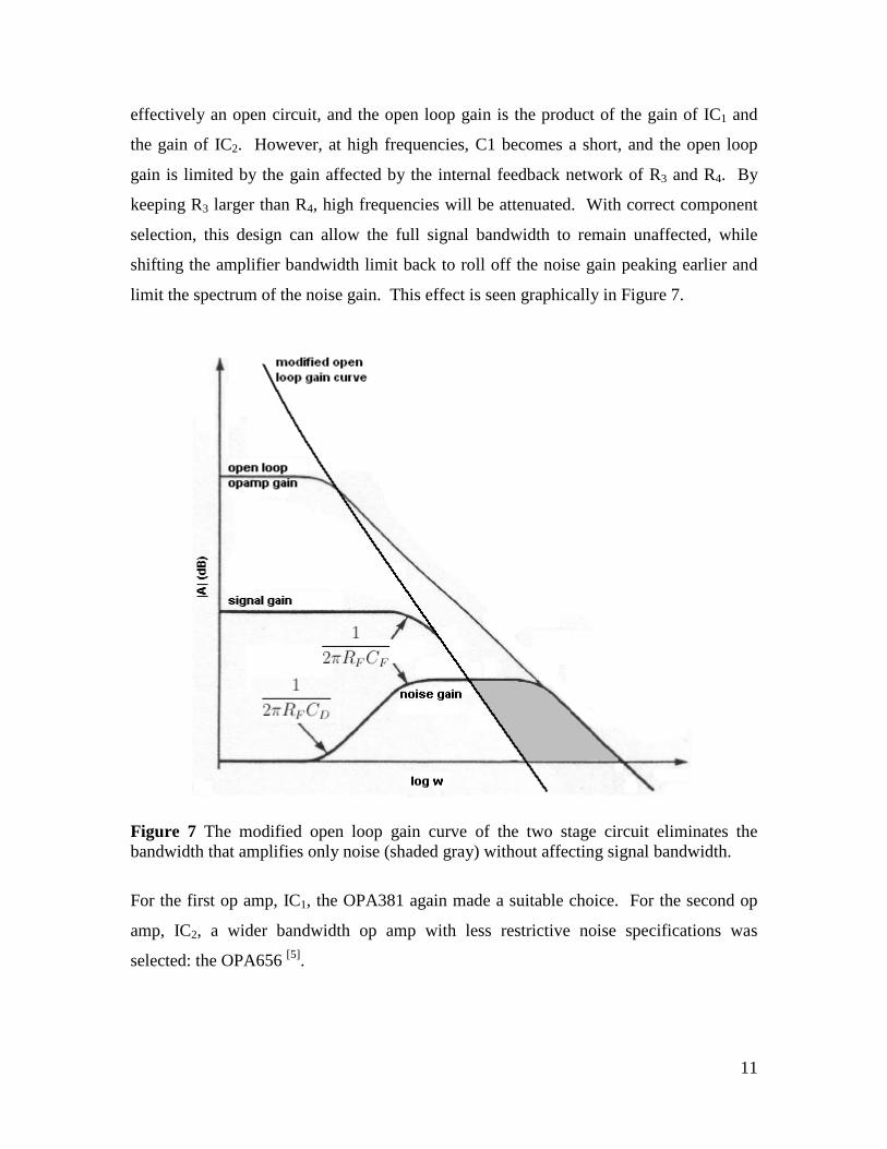
limit the spectrum of the noise gain. This effect is seen graphically in Figure 7.
Figure 7 The modified open loop gain curve of the two stage circuit eliminates the bandwidth that amplifies only noise (shaded gray) without affecting signal bandwidth.
For the first op amp, IC1, the OPA381 again made a suitable choice. For the second op
amp, IC2, a wider bandwidth op amp with less restrictive noise specifications was
selected: the OPA656 [5].

12
This circuit also included variable bias voltage, and selectable gain resistors, as in the
simple design. The same bias voltage error was present in this circuit as in the simple
circuit, and it was also corrected in the second prototype iteration. Power supply
regulation and decoupling was also improved in the second iteration, individual feedback
capacitors for each feedback resistor were added, and two different op amps were
selected for trial. IC1 was replaced by the AD8655 [15], and IC2 was replaced by the
AD8027 [16].
2.3.3 Differential Amplifier
The third design is shown in Figure 8 (full schematic in Appendix A). In this design, two
matched op amps provide equal amplification of the photocurrent, and the output of each
is fed into an instrumentation amplifier. This configuration utilizes the high common
mode rejection ratio of the instrumentation amplifier to eliminate noise common to both
signals. This is especially useful in rejecting power supply noise, electrostatic noise, and
magnetically coupled noise. This design requires careful trace length matching and
layout of components to be equidistant from sources of potential noise.
For this design, IC1 and IC2 were on a dual op amp chip, the AD8626 [17], and the
instrumentation amplifier was the AD8221 [18].

13
Figure 8 Differential design. The instrumentation amplifier IC3 has a high common mode rejection ratio, eliminating noise common to the circuit such as electrostatically and magnetically coupled noise and power supply noise.
2.3.4 Bootstrapped Cascode
After the first iteration of prototypes, a fourth design was added. The bootstrapped
cascode [12] uses a bipolar junction transistor to isolate the diode capacitance from the
feedback network of the op amp. This eliminates the noise gain peaking problem while
adding only a small amount of noise due to the transistor. The design is shown in Figure
9, and the full schematic is in Appendix A.

14
Figure 9 Bootstrapped Cascode [10]. The transistor Q1 isolates the photodiode capacitance CD from the amplifier, eliminating noise gain and allowing higher bandwidth.
In this design, Q1 transmits the photocurrent to the feedback resistor, but acts as a buffer
to separate the photodiode capacitance from the feedback network. In order to linearize
Q1, a small bias current at the base is needed. This is provided by Q2. Unfortunately, the
bias current required to linearize Q1 is larger than the photocurrent itself for the low range
of power detection, saturating the amplifier at high gain stages.
2.3.5 Passive Component Selection
The most critical part of component selection in this project is finding an appropriate op
amp, but choosing suitable passives is also important.
Most importantly, choosing the best feedback resistors is key to producing a detector that
will not drift or degrade over time. High precision is good, but stability is much more
important. Metal film and thick film through-hole resistors provide the best performance
characteristics. Metal film and thick film resistors are the least likely to have
manufacturing or damage defects, which can lead to 1/f pink noise in addition to Johnson

15
noise [14]. They also generally provide the best stability and thermal drift characteristics [12].
Also, choosing suitable capacitors is important. In this case, shunt resistance, stability,
and performance at different frequencies is the key. For the feedback capacitors,
stability, precision, and excellent performance throughout the frequency spectrum is
important. To achieve this, C0G/NP0 ceramic capacitors were used [12]. C0G/NP0
capacitors are manufactured from specific dielectric materials to have minimal
temperature dependence, vibration induced noise injection, and loss, and excellent high
frequency performance.
For decoupling, precision and stability are less critical, but covering the frequency
spectrum is important. Low frequency high amplitude spikes must be eliminated equally
as well as high frequency white noise. To achieve this, a combination of capacitors was
employed. To handle the low frequency and high voltage noise, large polarized
electrolytic capacitors were used on the power supply inputs. Electrolytic capacitors have
low shunt resistance and perform poorly at higher frequencies, however. To help in this
area, 10 µF tantalum capacitors and 0.1 µF ceramic capacitors were also used on the
power supply inputs, voltage regulator inputs and outputs, and op amp power supply pins.
Tantalum capacitors handle all frequencies relatively well, and ceramic capacitors are
particularly good at higher frequencies [12].
2.3.6 Housing Design
The completed photodetector system is intended to be mounted, at close range, onto the
MOT unit in the sponsor's lab. The light emanating from the MOT is focused through a
10 cm length 2.5 cm diameter tube by a lens, after which the light is divided by a beam
splitter and the two paths each enter photodetectors.
Figure 10 below shows a SolidWorks drawing of the photodetector mount system. The
physical specifications required the complete system (lens tube, beam splitter and two

16
photodetectors) to fit the MOT unit and have a clear line of sight to the atom cloud.
Minimum sizing was not set, but was desired to be as small as possible. The housing unit
purchased was bought as a stock manufactured aluminum shielding case and modified to
add the necessary holes using the project lab's water jet cutter. The beam splitter cube is
the largest component and set the critical size maximum for the housing. The circuit
board was designed to its minimum size and set parallel to the face of the beam splitter
cube to further reduce additional volume.
The photodetector was attached using cage mounts, which serve two purposes: it provides
a rigid mounting surface that ensures structural stability, and allows for up to 1.5 cm of
travel in order for the light source to be focused sharply on the photodiode. The cage
mounts were attached to the aluminum housing by sunken threaded machined holes in the
Thorlabs cage mount component. Drawings of the housing system are included below in
Figure 10.
Figure 10 Mechanical design drawing of detectors in the system.

17
2.4 Measurement Procedure
Careful and consistent measurements are crucial to establishing reliable performance
metrics and achieving accurate calibration. As such, the techniques used to obtain the
results presented in Section 2.5 are outlined here. The optical system used to produce the
signal used in the measurement of the noise, frequency response, and power calibration is
shown in Figure 11. The beam splitters (approximately 5% reflectivity) and neutral
density filter (approximately 12% transmission) were used to reduce the power of the
beam to suitable levels for the detector while remaining in a clean, linear region of the
laser output. The beam splitter was also used to produce a second beam incident on a
second, commercial photodetector made by New Focus [13]. This detector, labelled “NF
photodetector” in Figure 11, is a 125 MHz flat frequency response Silicon photodiode
photodetector used as a reference in the frequency response measurement. The current
driver used was a custom device with a tunable output current and an AC modulation
input. The modulation input, however, has a bandwidth limit of approximately 50 kHz.
To achieve laser modulation above this frequency, a simple custom laser driver board
was made to accept both a DC current and an AC voltage to modulate the laser voltage
directly. The schematic and explanation of this laser driver is contained in Appendix C.
The noise and frequency response measurements were performed with a 780 nm optical
bandpass filter installed on the detector.

18
Figure 11 Optical system used for characterization and calibration measurements.
2.4.1 Photodiode Responsivity vs. Position of Incident Light
Some photodiodes exhibit non-uniform responses across their detection area. To quantify
this non-uniformity for the FDS1010 photodiode used in this project, a 780 nm
semiconductor laser was focused onto a specific part of the photodiode, and the voltage
across the photodiode was measured directly using an oscilloscope as the position of the
photodiode was systematically varied. To avoid obfuscating the results by using an
amplifier, the photodiode was connected directly to the oscilloscope inputs to measure the
photodiode response. The photodetector was mounted on an x-y-z stage used to move the
photodiode slowly across the focused beam location, and the output was measured at
each positional increment across the cross sectional detection area of the photodiode.

19
The behaviour of the photodiode corresponding to variation in incident beam spreading
was also measured. The beam was focused at the centre of the photodiode, and the stage
was used to move the photodiode away from the focal plane, spreading the light intensity
across a successively larger area of the photodiode. The output was measured at several
positions to determine if, as expected, it remained constant while the full beam remained
on the photodiode detection area.
2.4.2 Noise
For each prototype and the final photodetector, the noise in each gain stage was
measured. The noise level was measured using the digital oscilloscope to isolate the AC
portion of the signal, which comprises the noise. The noise was measured at varying DC
signals within the dynamic range of each gain stage. To provide the photodetector with a
DC signal, the laser was driven at a constant current, and the beam passed through the
optical system shown in Figure 11. To vary the intensity seen at the detector, the neutral
density filter was added or removed as necessary, and the iris at the detector partially
closed to allow only part of the incident beam. This mitigates issues of optical noise on
the laser varying at different input currents that were observed when the intensity at the
detector was varied by changing the input current to the laser.
The noise levels quoted are root mean squared (RMS) voltages. The RMS voltage of the
AC signal was measured using the built in function on the digital oscilloscope.
2.4.3 Frequency Response
The frequency response was measured by modulating the input to the 780 nm laser with
varying modulation frequencies, from DC to 300 kHz, and comparing the detector output
to that of a high bandwidth flat frequency response New Focus photodetector. Below 50
kHz, the modulation was achieved by connecting an AC voltage supply to the modulation
input of the custom current driver used. Due to bandwidth limitations on the modulation

20
input of the current driver, above 50 kHz modulation was achieved instead by connecting
the function generator to the custom built laser driver board AC input, which modulates
the laser voltage directly. Further explanation of the laser driver board is included in
Appendix C.
To measure the frequency response, the frequency of modulation was varied, and the AC
amplitude of the output of both detectors recorded. The amplitude of modulation was
measured using the built in amplitude measurement function of the digital oscilloscope.
Then, at each modulation frequency, the amplitude of the project detector was divided by
the amplitude of the reference detector. Normalizing the results to the lowest frequency
measured and converting the results to decibels yields the results shown in Section 2.5.
In some cases, the full frequency response was not required, but only an estimate of the 3
dB bandwidth. In this case, a measurement of the relative AC amplitudes of the two
detectors was taken at a very low frequency – typically 10 Hz – and the frequency was
adjusted upwards until the relative amplitudes reach half of the initial value. This
frequency is the 3 dB bandwidth.
2.4.4 Photodetector Power Calibration
Power calibration was a sensitive process, requiring careful attention to calibration of
optical components and consistency in measurement techniques. To attenuate the optical
signal to ranges useful for power calibration in all gain stages, several optical components
were employed. In addition to the optical setup shown in Figure 11, two mirrors and a
second lens were added so that the detector was facing away from the laser. This was
done to minimize the amount of light resulting from reflection and diffraction of the laser
outside the primary beam path incident on the detector. Also, several neutral density
filters were placed in the beam path as needed to attenuate the optical signal to the
desired range. The measurements were performed by reading the detector output, then
placing the power metre directly in front of the detector and reading the power metre
output. The power calibration was performed without the bandpass filter on the
21
photodetector, and without the neutral density filter attached to the power metre. Power
calibration was performed at 780 nm.
2.4.5 Problems and Limitations
The most persistent problem during measurements was separating electrical noise from
optical noise. Optical noise, in the context of characterizing a photodetector, is
considered signal; however, isolating electrical noise from optical noise proved to be
difficult. In particular, because of the very high sensitivity of the higher gain stages,
optical noise in these stages can be inadvertently amplified, artificially inflating the noise
level of the photodetector.
Sources of optical noise include lighting in the room, noise on the current source driving
the laser, laser noise caused by competing modes with similar gain stochastically
switching, and laser far field reaching the detector. Other external noise sources include
inherent oscilloscope noise, electro-magnetic noise coupled into the cabling, and power
supply noise. Power supply noise at 60 Hz and harmonics was visible on the output of
the detector, but appeared to be a result of both noise on the detector itself, and noise on
the laser driver transferring onto the laser output, and thus appearing as part of the signal.
Noise levels on the laser output were also observed to vary at different current set points,
likely due to competing modes of nearly the same gain stochastically switching between
each other resulting in fluctuating output power. To mitigate this problem, the laser was
driven at a constant current observed to have consistently good noise performance, and
the intensity at the detector varied by changing the diameter of the aperture to the
photodiode with the iris so as to limit the amount of the beam incident on the photodiode.
Some difficulties were also encountered with the frequency response measurements. The
modulation signal was obscured partially by noise on both the project photodetector and
the reference photodetector, and the error on the measurements of the relative amplitudes
of the modulation signal was high. The built in amplitude measurement function on the

22
digital oscilloscope was helpful, but exhibited some digital quantization noise, and in
cases of low modulation amplitude, sometimes had trouble determining accurate
amplitudes due to the noise on the signal. Establishment of the general trend and shape
of the frequency responses and the 3 dB bandwidths was, however, a repeatable process.
The primary obstacle in power calibration was reaching all ranges of power necessary,
and isolating background noise. Because of unusual laser behaviour in many ranges of
input currents, achieving arbitrary input power by means of varying the input current
alone was not possible. To achieve the required power range, optical attenuation using
neutral density filters and beam splitters was used in conjunction with variable input
current to vary the input power. A second problem was the background noise apparently
caused by the far field of the laser; this problem was particularly prevalent at higher gain
stages. When the detector was facing the laser, blocking the primary beam and varying
the current at the laser resulted in clear, significant variation on the detector output
corresponding directly to the changes in the laser current. To help eliminate this
problem, mirrors were used to direct the beam back in the opposite direction from which
it came so that the detector was facing away from the laser. This minimized the
background noise caused by reflections and diffractions of the far field. Another problem
encountered was the effect of the bandpass filter. The 780 nm optical bandpass filter
attenuated the signal significantly (approximately 70%), reducing the sensitivity of the
detector. Also, the orientation of the filter was measured to be very important to how
much the signal was attenuated. The angle that the beam hit the filter severely affects the
amount of light the filter allows to pass. To avoid this problem, the calibration was
performed without the bandpass filter. To eliminate the effect of background noise away
from 780 nm, and allow measurements at very low scale on the detector, the calibrations
were performed in complete darkness.
2.5 Results
The different prototypes were evaluated and compared based primarily on three
performance metrics: frequency response, noise, and reliability. The frequency response
23
and noise were measured quantitatively, while the reliability was evaluated by the authors
qualitatively through careful observation and notation of glitches, such as oscillation,
railed output, inconsistent output, or altogether failure to function.
The specified noise values are root mean squared (RMS) voltages, and unavoidably
include some amount of optical noise which cannot be completely identified and isolated.
Also, power supply noise at 60 Hz and its harmonics were present in some amount on all
measurements, further artificially inflating the noise figures. This power supply noise is
present both on the circuit itself, and as a modulation signal on the laser due to noise on
the current supply driving the laser. This was determined by observing the output at high
gain stages, where 60 Hz noise was present in significantly larger amounts than at lower
gain stages, indicating that it is a part of the optical input signal being amplified.
For these reasons, the noise performance of all circuits is in fact slightly better than
specified; the values quoted are based on the total AC voltage superimposed on the DC
signal, regardless of the source of the AC signal.
2.5.1 Photodiode Responsivity vs. Position
The photodiode showed a very uniform responsivity in the x direction (moving parallel to
the base of the photodiode with the wire outputs). The largest variation in the x direction
was 0.5%. In the y direction, the responsivity increased slightly as the beam became
closer to the wire outputs. The largest variation in the y direction was 2.5%.
2.5.2 First Iteration Simple Prototype
The first iteration of the simple prototype performed reliably and predictably. The
frequency response of the circuit for each of the four gain stages is shown in Figure 12.
The resonant peaks in each of the curves are a result of a similar resonance present in the
frequency response of the OPA381 op amp [4]. These peaks are present at some level in
all of the frequency response curves for circuits that include the OPA380 or OPA381.

24
(a)
103
104
105
106
107
-40
-30
-20
-10
0
10
20
30
frequency (Hz)
dB
frequency response of simple prototype, Cf = 4.7 pF
10k
100k
1M10M
-3 dB
(b)
Figure 12 Simple prototype basic circuit (a) and first iteration frequency response, CF = 4.7 pF (b). The resonant peaks seen in this and following frequency responses are a direct result of resonant peaks in the OPA380 [4] and OPA381 [19] closed loop gain curves.

25
After a brief qualitative power calibration to learn the rough range of the photodiode
sensitivity, it was determined that the circuit response was roughly linear from 0 to
roughly 4.4 V, just below the positive rail for the OPA381 when it is powered on the
positive supply by 5 V. It was also determined that the 10 kΩ gain stage would be
unnecessary because the upper optical power of interest specified in the project objectives
(10 µW) was easily covered by higher gain stages. Also, to improve the signal noise ratio
at the low end of the optical power of interest (10 nW), a higher gain resistor of 100 MΩ
was added to future prototypes.
The noise at each relevant gain stage is shown in Table 1. There was a strong harmonic
present at roughly 270 Hz, which remained unexplained.
Gain RMS Voltage Noise 100 kΩ 2.5 mV 1 MΩ 3 mV
10 MΩ 4 mV
Table 1 Simple prototype first iteration RMS noise, CF = 4.7 pF.
Qualitative testing with the feedback capacitor removed (some feedback capacitance will
remain due to the stray capacitance associated with the feedback resistor and circuit
board) showed the expected results. The bandwidth increased significantly – from
roughly 20 kHz to roughly 60 kHz at 10 MΩ gain – but the noise also increased
significantly, going from 4 mV RMS to about 20 mV RMS.
Biasing the photodiode in this circuit did not improve the noise performance; in fact, it
weakened it. Due to an error in the biasing scheme design, the biasing was achieved by
shorting the photodiode cathode to the -5 V power supply input line. One possible
explanation considered for the poor performance with this biasing scheme was that the
bias voltage was unregulated, and potentially noisy. To test this, the biasing design error
was updated in the second iteration; however, biasing the photodiode still did not
improve the noise performance for the simple design.

26
2.5.3 First Iteration Two Stage Prototype
Initial testing of the two stage prototype with no bias voltage applied to the photodiode
showed stable operation in the higher gain stages, but the circuit oscillated rail to rail in
the 100 kΩ gain stage. Applying a -5 V bias voltage improved the performance of all
stages, and allowed stable operation at 100 kΩ. Quick tests of bandwidth with and
without bias demonstrated that the frequency response of the circuit was unaffected by
bias voltage, as expected. Because the two stage prototype showed occasional instability,
a larger feedback capacitor of 10 pF was used for testing to help reduce the possibility of
instability by reducing noise gain, which can initiate oscillation.
The frequency response for the two stage prototype is shown in Figure 13. The
frequency response was measured with no bias voltage for the 1 MΩ and 10 MΩ stages,
but to avoid oscillation and allow for testing, with a -5 V bias applied for the 100 kΩ
stage.
(a)

27
103
104
105
106
-20
-15
-10
-5
0
5
frequency (Hz)
dB
frequency response of two stage prototype, Cf = 10 pF
100k,Vb = -5V
1M, Vb = 0
10M, Vb = 0
-3 dB
(b)
Figure 13 Two stage prototype basic schematic (a) and first iteration frequency response with Cf = 10 pF (b).
Aside from allowing stable operation in the 100 kΩ gain stage, applying bias voltage to
the photodiode improved the noise performance of the circuit, and caused a dark current
to be emitted from the photodiode, leading to an output voltage on the detector even
when no input signal is present on the photodiode. This dark output was negligible at low
gain, but when amplified more strongly in the higher gain stages, became significant.
The dark output at each of the gain stages is shown in Table 2.

28
Gain Dark Output 100 kΩ < 5 mV 1 MΩ 20 mV
10 MΩ 200 mV 100 MΩ 1.92 V
Table 2 Two stage prototype dark current output with -5 V bias on photodiode
The dark current is particularly problematic at the 100 MΩ gain stage, where it removes
nearly half of the dynamic range of the op amp.
The noise in the circuit both with and without bias voltage is shown in Table 3.
Gain Bias Voltage RMS Voltage Noise
100 kΩ 0 V Oscillating 100 kΩ -5 V 1.5 mV 1 MΩ 0 V 4.5 mV 1 MΩ -5 V 2.5 mV
10 MΩ 0 V 5 mV 10 MΩ -5 V 2.5 mV
100 MΩ 0 V 5 mV 100 MΩ -5 V 4.5 mV
Table 3 Two stage prototype first iteration RMS noise, CF = 10 pF.
The circuit had some glitches. Oscillation without bias voltage occurred always in the
100 kΩ gain stage, and with smaller feedback capacitors, also occurred sporadically in
other gain stages. Also, the output of the circuit occasionally jumped to the positive rail.
The circuit performed well from a noise and bandwidth perspective, but showed some
unreliability. In an effort to improve this, the second iteration was tweaked and the op
amps replaced.
2.5.4 Differential Prototype
The differential based prototype performed very reliably, but did not meet expectations in
noise performance. The frequency response of each gain stage is shown in Figure 14.

29
(a)
103
104
105
106
-10
-5
0
5
10
15
20
frequency (Hz)
dB
frequency response of differential prototype, Cf = 4.7 pF
100k
1M10M
-3 dB
(b)
Figure 14 Differential prototype basic schematic (a) and frequency response with CF = 4.7 pF (b).
30
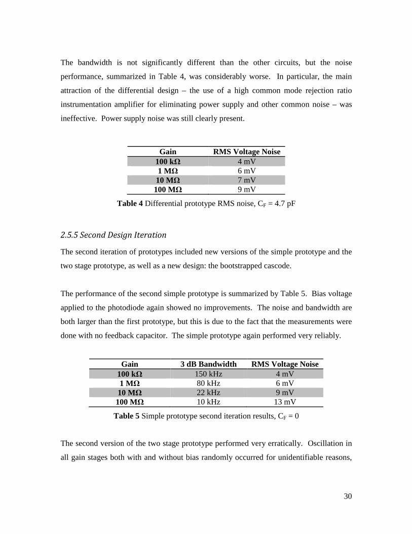
The bandwidth is not significantly different than the other circuits, but the noise
performance, summarized in Table 4, was considerably worse. In particular, the main
attraction of the differential design – the use of a high common mode rejection ratio
instrumentation amplifier for eliminating power supply and other common noise – was
ineffective. Power supply noise was still clearly present.
Gain RMS Voltage Noise 100 kΩ 4 mV 1 MΩ 6 mV
10 MΩ 7 mV 100 MΩ 9 mV
Table 4 Differential prototype RMS noise, CF = 4.7 pF
2.5.5 Second Design Iteration
The second iteration of prototypes included new versions of the simple prototype and the
two stage prototype, as well as a new design: the bootstrapped cascode.
The performance of the second simple prototype is summarized by Table 5. Bias voltage
applied to the photodiode again showed no improvements. The noise and bandwidth are
both larger than the first prototype, but this is due to the fact that the measurements were
done with no feedback capacitor. The simple prototype again performed very reliably.
Gain 3 dB Bandwidth RMS Voltage Noise 100 kΩ 150 kHz 4 mV 1 MΩ 80 kHz 6 mV
10 MΩ 22 kHz 9 mV 100 MΩ 10 kHz 13 mV
Table 5 Simple prototype second iteration results, CF = 0
The second version of the two stage prototype performed very erratically. Oscillation in
all gain stages both with and without bias randomly occurred for unidentifiable reasons,

31
and the circuit output often railed at the positive op amp supply. When the circuit
worked, it performed similarly to the first iteration.
The last prototype, the bootstrapped cascode, showed very good noise performance at
low gain, but was permanently saturated at all gains higher than 100 kΩ. This is due to
the fact that the “bootstrapping” part of the circuit, which linearizes the transistor Q1 of
Figure 9 by supplying a small bias current to the base, supplies a current that is large
enough to saturate the amplifier without any photocurrent.
2.5.6 Final Design Selection
Based on the results of the first design iteration, the differential amplifier was abandoned
due to poor noise performance, and the simple and two stage designs were carried
through to a second, tweaked design. The goal was to improve the reliability of the two
stage design, make small tweaks to the simple design for further testing, and investigate
the bootstrapped cascode design. The bootstrapped cascode could potentially be tweaked
to be suitable for the intended application, but due to the complexity of the circuit and
limited time frame for completion, immediately reliable operation was deemed
paramount.
The selection between the simple prototype and the two stage design was made based on
the same philosophy. The two stage amplifier could likely be tweaked and tested to the
point of providing a detector with the same reliability as the simple design, and based on
the idea of the circuit and the test results from the first iteration, likely perform at a higher
level. However, given the time constraints and necessity of producing a working final
product, as well as the fact that the simple prototype performed very reliably at a level
very close to meeting all of the project objectives, the two stage design was dropped in
favour of the simple design.

32
Figure 15 Final design basic schematic. The simple transimpedance amplifier performed most reliably.
2.5.7 Final Circuit, 1 pF Feedback Capacitance
The final circuit was professionally fabricated by Canadian Circuits. The schematic and
PCB layout are shown in Appendix B. For baseline testing, the circuit was characterized
fully with a 1 pF capacitor. Also, to best achieve the project objectives, a new set of gain
resistors was chosen: 1 MΩ, 10 MΩ, 50 MΩ, and 100 MΩ. The motivation for the new
choices was to provide the ability for very low noise, high sensitivity DC measurements
in which bandwidth is not a concern, while still allowing for the possibility of faster high
sensitivity measurements where some noise performance is sacrificed.
The frequency response of the final circuit with a 1 pF feedback capacitor and the
OPA380 is shown in Figure 16.

33
101
102
103
104
105
106
-25
-20
-15
-10
-5
0
5
frequency (Hz)
dB
frequency response of final circuit, Cf = 1 pF, OPA380
1M
10M
50M100M
-3 dB
Figure 16 Final circuit frequency response, OPA380, CF = 1 pF.
The noise performance was once again tested both with and without bias voltage applied
to the photodiode. The circuit was also tested with both the OPA380 and OPA381 for
direct comparison. The results are summarized in Table 6.
Gain Bias Voltage RMS Voltage Noise
(OPA380) RMS Voltage Noise
(OPA381) 1 MΩ 0 V 7.4 mV 5.2 mV 1 MΩ -5 V 7.2 mV -
10 MΩ 0 V 12 mV 8.6 mV 10 MΩ -5 V 21 mV - 50 MΩ 0 V 16 mV 9.6 mV 50 MΩ -5 V 27 mV -
100 MΩ 0 V 23 mV 10 mV 100 MΩ -5 V 29 mV -
Table 6 Final circuit comparison of RMS noise levels, CF = 1 pF.
34
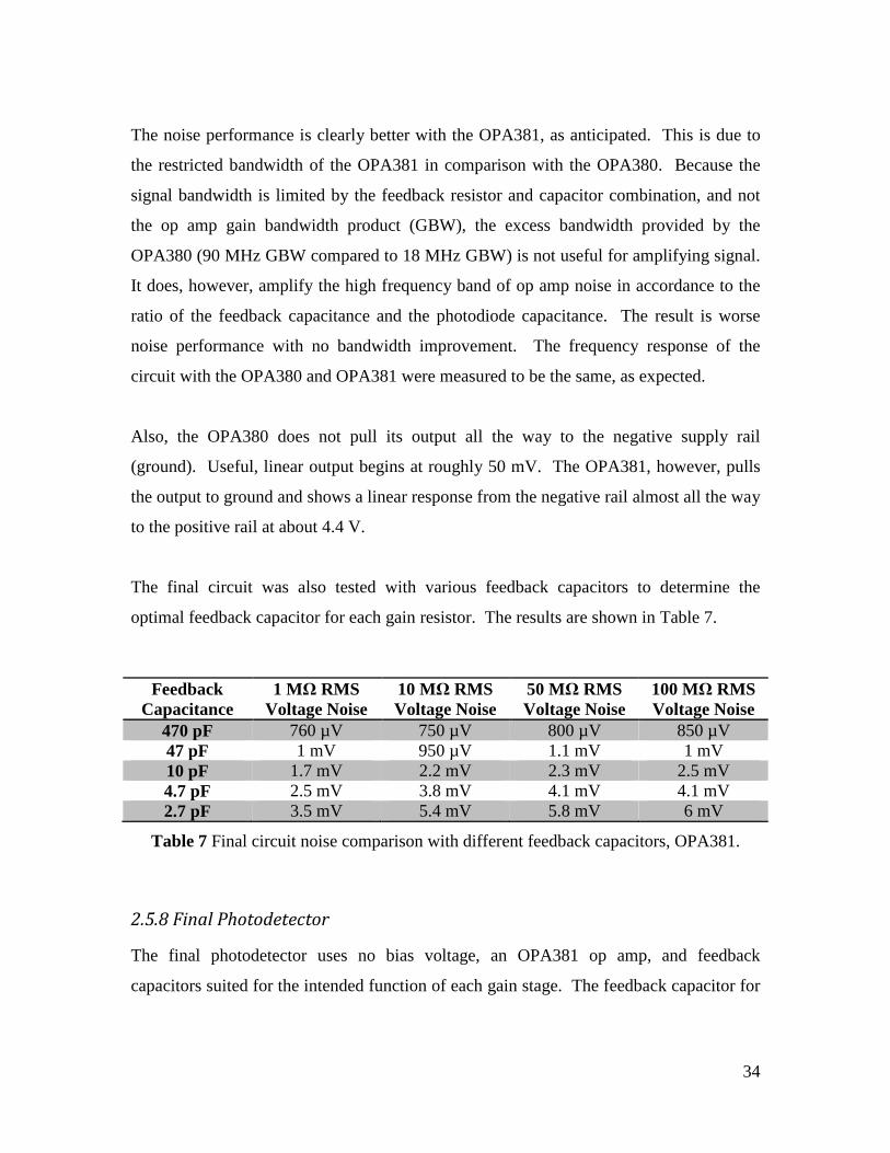
The noise performance is clearly better with the OPA381, as anticipated. This is due to
the restricted bandwidth of the OPA381 in comparison with the OPA380. Because the
signal bandwidth is limited by the feedback resistor and capacitor combination, and not
the op amp gain bandwidth product (GBW), the excess bandwidth provided by the
OPA380 (90 MHz GBW compared to 18 MHz GBW) is not useful for amplifying signal.
It does, however, amplify the high frequency band of op amp noise in accordance to the
ratio of the feedback capacitance and the photodiode capacitance. The result is worse
noise performance with no bandwidth improvement. The frequency response of the
circuit with the OPA380 and OPA381 were measured to be the same, as expected.
Also, the OPA380 does not pull its output all the way to the negative supply rail
(ground). Useful, linear output begins at roughly 50 mV. The OPA381, however, pulls
the output to ground and shows a linear response from the negative rail almost all the way
to the positive rail at about 4.4 V.
The final circuit was also tested with various feedback capacitors to determine the
optimal feedback capacitor for each gain resistor. The results are shown in Table 7.
Feedback Capacitance
1 MΩ RMS Voltage Noise
10 MΩ RMS Voltage Noise
50 MΩ RMS Voltage Noise
100 MΩ RMS Voltage Noise
470 pF 760 µV 750 µV 800 µV 850 µV 47 pF 1 mV 950 µV 1.1 mV 1 mV 10 pF 1.7 mV 2.2 mV 2.3 mV 2.5 mV 4.7 pF 2.5 mV 3.8 mV 4.1 mV 4.1 mV 2.7 pF 3.5 mV 5.4 mV 5.8 mV 6 mV
Table 7 Final circuit noise comparison with different feedback capacitors, OPA381.
2.5.8 Final Photodetector
The final photodetector uses no bias voltage, an OPA381 op amp, and feedback
capacitors suited for the intended function of each gain stage. The feedback capacitor for

35
each gain stage and the rotary switch position to select the desired gain stage are shown
in Table 8.
Gain Feedback Capacitance Switch Position 1 MΩ 10 pF 1
10 MΩ 2.7 pF 2 50 MΩ 1 pF 3
100 MΩ 47 pF 4
Table 8 Final detector gain resistances, feedback capacitances, and switch positions
The frequency response of the final photodetector in its final configuration is shown in
Figure 17.
100
101
102
103
104
105
106
-25
-20
-15
-10
-5
0
5
frequency (Hz)
dB
frequency response of final photodetector
1M
10M
50M100M
-3 dB
Figure 17 Final detector frequency response. The 100 MΩ gain stage is intended for high precision DC measurements, while the 50 MΩ gain stage is intended to be a high speed high sensitivity setting that sacrifices noise performance.

36
Table 9 summarizes the key performance metrics of the final photodetector.
Gain 3 dB Bandwidth RMS Voltage Noise 1 MΩ 60 kHz 1.8 mV
10 MΩ 17 kHz 5.0 mV 50 MΩ 2.5 kHz 8.0 mV
100 MΩ ~10 Hz 1.0 mV
Table 9 Final detector bandwidth and noise summary.
The feedback capacitors were selected to optimize each gain stage. The 1 MΩ and 10
MΩ gain stages are general purpose, optimized for a combination of good noise
performance and high bandwidth. The 50 MΩ gain stage is intended to be a high
sensitivity setting that provides enough bandwidth for reliable measurement stability on
the millisecond scale while maintaining a reasonable noise level. The 100 MΩ gain is
intended to be a setting used for DC measurement only, providing very high sensitivity
and excellent noise performance. Tweaking the capacitors further can alter the
noise/bandwidth trade-off to whatever is desirable, without affecting the power
calibration.
The input power to output voltage calibration for the first completed detector, labelled
Detector 2, is shown in Figures 18 through 21. Linearity is achieved in all gain stages
from the negative rail up to near the positive rail.

37
Fig
ure
18 P
ower
cal
ibra
tion
curv
e fo
r D
ete
ctor
2,
780
nm, 1
MΩ
gai
n.
0 2 4 6 8 10 120
0.5
1
1.5
2
2.5
3
3.5
4
4.5
5
Power (uW)
Det
ecto
r O
utpu
t (V
)Detector 2 Output Calibration: 780 nm, 1 MOhm
data
linear fit: V = 0.5491041*P(uW) + 0.0067734 V

38
Fig
ure
19 P
ower
cal
ibra
tion
curv
e fo
r D
ete
ctor
2,
780
nm, 1
0 MΩ
gai
n.
0 100 200 300 400 500 600 700 800 900-0.5
0
0.5
1
1.5
2
2.5
3
3.5
4
4.5
Power (nW)
Det
ecto
r O
utpu
t (V
)
Detector 2 Power Calibration: 780 nm, 10 MOhm
data
linear fit: V = 0.0054553 * P(nW) - 0.0137041

39
Fig
ure
20 P
ower
cal
ibra
tion
curv
e fo
r D
ete
ctor
2,
780
nm, 5
0 MΩ
gai
n.
0 20 40 60 80 100 120 140 160 180 200-0.5
0
0.5
1
1.5
2
2.5
3
3.5
4
4.5
Power (nW)
Det
ecto
r O
utpu
t (V
)
Detector 2 Output Calibration: 780 nm, 50 MOhm
data
linear fit: V = 0.0277525*P(nW) - 0.0719096

40
Fig
ure
21 P
ower
cal
ibra
tion
curv
e fo
r D
ete
ctor
2,
780
nm, 1
00
MΩ
gai
n.
0 10 20 30 40 50 60 70 80 90-0.5
0
0.5
1
1.5
2
2.5
3
3.5
4
4.5
Power (nW)
Det
ecto
r O
utpu
t (V
)
Detector 2 Output Calibration: 780 nm, 100 MOhm
data1
linear fit: 0.0547081*P(nW) - 0.1182388

41
The signal to noise ratio (SNR) is well above the target specification of 40 dB for the
majority of the power detection range specified in the project objectives (10 nW to 10
µW). The SNR at the minimum power of interest, 10 nW, is roughly 53 dB. The lowest
values of SNR in the detection range of interest occur when the detector is operated in a
region where the amplifier output is in the low portion of its full output scale. These
necessarily occur at boundaries between gain stages where the higher gain saturates and
the next lower gain stage must be used. The boundary between 100 MΩ and 50 MΩ
occurs at roughly 80 nW; the SNR in the 50 MΩ stage at 80 nW is roughly 48 dB. The
boundary between 50 MΩ and 10 MΩ occurs at roughly 155 nW; the SNR in the 10 MΩ
stage at 155 nW is roughly 43 dB. The boundary between 10 MΩ and 1 MΩ occurs at
roughly 780 nW; the SNR in the 1 MΩ stage at 780 nW is roughly 44 dB. Thus, the
minimum signal to noise ratio of the detector through the power range of interest is 43
dB, and the SNR is normally much higher. However, in the highest gain stage, the
bandwidth is very limited. For fast, high sensitivity measurements, the 50 MΩ gain stage
must be used. At 10 nW, the SNR is roughly 30 dB.

42
3 Conclusions
Prior to completion, the project went through various stages. First, a set of initial
prototypes were designed and fabricated. Following this, each prototype was tested and
characterized for comparison, and after evaluation of these results, a second round of
prototypes was issued. Following the characterization of this second iteration design set,
a basic transimpedance amplifier design was selected for the final application based on
test results which showed competitive performance in noise and bandwidth and extremely
high reliability. Design, PCB layout, and fabrication of the final circuit took place in
conjunction with a mechanical design encompassing the housing and integration of the
detectors into existing optical systems. Finally, the final circuits were populated, tested,
characterized, and calibrated, before being placed into the systems for which they were
designed.
The final product in large part met the objectives specified at the outset of the project.
The noise performance achieved was good, with noise levels measured at 1.8 mV RMS
for the 1 MΩ gain stage, 5 mV RMS for the 10 MΩ gain stage, 8 mV RMS for the 50
MΩ gain stage, and 1 mV RMS for the 100 MΩ gain stage. The noise performance for
each gain stage was defined largely by the combination of the feedback resistance and
capacitance; better noise performance was achieved in the 100 MΩ gain stage than the 50
MΩ gain stage by including a larger feedback capacitor, although this sacrifices
significant bandwidth. The minimum signal to noise ratio (SNR) throughout the
detection range was 43 dB, clearing the objective of 40 dB. The optimal SNR at the
lowest power of interest, 10 nW, was 57 dB, and the SNR throughout the majority of the
detection range is above 60 dB, achieving a maximum of 73 dB. The detector is able to
meaningfully read powers below 1 nW, exceeding the range of power required, although
at 1 nW the SNR is only 37 dB. The sensitivity and adjustable gain targets were met and
exceeded.
The bandwidth target was only partially achieved. Due to the high noise resulting from
the very large photodiode capacitance and high gain required to achieve the desired

43
sensitivity, the bandwidth specification proved difficult to meet without completely
sacrificing noise performance. At the two lower gain stages, 1 MΩ and 10 MΩ, the
bandwidth specification was exceeded, with 3 dB bandwidths of 60 and 17 kHz,
respectively. However, at the higher gain stages, the bandwidth and noise trade-off
suffered. As a compromise solution, two high sensitivity gain stages were provided: a
100 MΩ stage with very low bandwidth (~10 Hz) but very low noise for high precision
slow measurements, and a 50 MΩ stage with higher bandwidth (2.5 kHz) and higher
noise for less precise faster measurements. Although 2.5 kHz does not meet the 10 kHz
bandwidth target, it still allows measurement rise and fall times fast enough to be stable
within one millisecond. The minimum signal to noise ratio in this stage, occurring at the
minimum power of interest, 10 nW, falls slightly short of the 40 dB specification at 36
dB. Thus, the objective specifications are not simultaneously met throughout the entire
detection range, but are met for the large majority of the detection range.
The final detectors employ large area 1 cm2 FDS1010 photodiodes [20], allowing easy
alignment even at the very low optical power expected. The detectors were also
calibrated for 780 nm and 671 nm. The final product includes a compact housing,
combined with optical mounts allowing easy implementation into any optical system, an
iris and filter built on, and the desired BNC output and standard lab power supply
connection interface.

44
4 Recommendations
Although the photodetectors are complete and form a final product that will not be
altered, recommendations can be made about how to proceed with implementing them
into optical systems and how to potentially improve the design for future projects.
Isolating optical noise from the signal using bandpass filters should be more closely
investigated. Because the bandpass filters attenuate strongly even at the pass frequency,
the sensitivity and signal to noise ratio will be negatively affected. More importantly,
bandpass filters show alignment sensitivity that would impact the calibration factor
dependent on the orientation. Lens tubes may be a more effective means of isolating
optical noise.
If improvements to the design are desired for future work, the authors recommend
investing further time in the two stage circuit (Figure 6) and the bootstrapped cascode
(Figure 9). The two stage circuit would likely require testing more op amps, tweaking
component values, and identifying conditions leading to oscillation. The bootstrapped
cascode circuit could also potentially exceed the performance of the design used in this
project, but would likely require much more effort to achieve the performance. Finding
transistors which have very low operating currents would be helpful in eliminating the
problem of the bias current overrunning the signal current.
For simple adjustments to the bandwidth/noise trade-off, the feedback capacitors for each
gain resistor can be replaced with different value capacitors as necessary. In the final
schematic and PCB layout of Figures 28 and 29, respectively, these capacitors are
labelled C2, C3, C8, and C9. Adjusting the capacitor to a higher value will result in
improved noise performance, but decreased bandwidth, and vice versa.

45
Appendix A: Prototype Schematics Schematics from all of the prototypes tested are included below.
Figure 22 Simple prototype first iteration schematic.

46
Figure 23 Two stage prototype first iteration schematic.

47
In the first iteration simple and two stage designs, the bias voltage scheme contains an
error. Potentiameter R9 in both schematics sets the bias voltage through a jumper
allowing the user to choose a bias voltage set by R9 or ground. The wiper of the
potentiometer should in both cases be buffered before connecting to the jumper. This
error is corrected in the second iteration of both designs.
Figure 24 Differential prototype schematic.
48
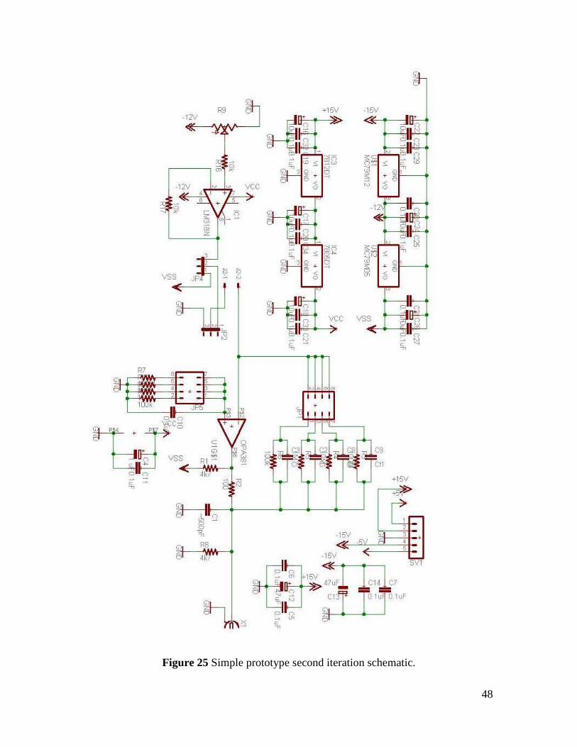
Figure 25 Simple prototype second iteration schematic.

49
Figure 26 Two stage prototype second iteration schematic.
50
Differences between the first and second iteration of the simple and two stage designs
include the addition of a buffer amplifier LM318N to correct the biasing error of the first
iteration, individual feedback capacitors for each gain resistor, better power supply
regulation and decoupling, and in the two stage case, new op amps.
Figure 27 Bootstrapped cascode prototype schematic.

51
Appendix B: Final Schematic and PCB Layout
Figure 28 Final circuit schematic.
52
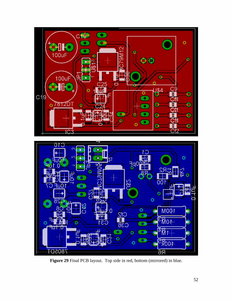
Figure 29 Final PCB layout. Top side in red, bottom (mirrored) in blue.

53
Appendix C: Laser Driver Board The laser driver was built to accept an input current on one input and transmit it directly
to the laser, and accept an AC voltage on a second input and modulate the laser directly.
It was designed to work specifically with the custom built current source available for
driver the laser. To avoid having the current source absorb all the AC voltage applied to
the AC input, an inductor was placed in series with the current input. The schematic is
shown below in Figure 30.
Figure 30 Laser driver schematic.
The board used was modified from a previous similar laser driver. The AC voltage input
was not useful at low frequencies, where, despite the inductor, the voltage would be
absorbed by the current driver connected to the “current in” input. To avoid this problem,
at low frequency (less than approximately 50 kHz) the AC voltage source was connected
to the bandwidth limited AC modulation input on the current driver, and at higher
frequencies it was connected to the AC voltage in input on the laser driver. In both cases,
the amplitude of modulation on the laser current was frequency dependent. To eliminate
this unknown variation, the frequency response measurements used a New Focus 125
MHz photodetector as a reference, as described in Section 2.4.3.

54
Appendix D: Power Calibration Curves
10 20 30 40 50 60 70 80 90 1000
0.5
1
1.5
2
2.5
3
3.5
4
4.5
power (nW)
volta
ge (
V)
Detector 1 power calibration, 780 nm, 100 MOhm
y = 0.053267*x - 0.99761
data 1
linear
20 40 60 80 100 120 140 160 1800
0.5
1
1.5
2
2.5
3
3.5
4
4.5
power (nW)
volta
ge (
V)
Detector 1 power calibration, 780 nm, 50 MOhm
y = 0.027592*x - 0.50898
data 1
linear

55
0 100 200 300 400 500 600 700 800-0.5
0
0.5
1
1.5
2
2.5
3
3.5
4
4.5
power (nW)
volta
ge (
V)
Detector 1 power calibration, 780 nm, 10 MOhm
y = 0.0056773*x - 0.14375
data 1
linear
0 1000 2000 3000 4000 5000 6000 7000 8000-0.5
0
0.5
1
1.5
2
2.5
3
3.5
4
4.5
power (nW)
volta
ge (
V)
Detector 1 power calibration, 780 nm, 1 MOhm
y = 0.0005639*x - 0.0091931
data 1
linear
Figure 31 Detector 1 Power Calibration Curves

56
0 10 20 30 40 50 60 70 80 900
0.5
1
1.5
2
2.5
3
3.5
4
4.5
power (nW)
volta
ge (
V)
Detector 3 power calibration, 780 nm, 100 MOhm
y = 0.053089*x - 0.25083
data 1
linear
0 20 40 60 80 100 120 140 1600
0.5
1
1.5
2
2.5
3
3.5
4
4.5
power (nW)
volta
ge (
V)
Detector 3 power calibration, 780 nm, 50 MOhm
y = 0.026649*x - 0.13132
data 1
linear
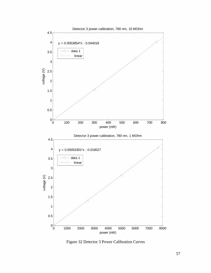
57
0 100 200 300 400 500 600 700 8000
0.5
1
1.5
2
2.5
3
3.5
4
4.5
power (nW)
volta
ge (
V)
Detector 3 power calibration, 780 nm, 10 MOhm
y = 0.0053854*x - 0.044018
data 1
linear
0 1000 2000 3000 4000 5000 6000 7000 80000
0.5
1
1.5
2
2.5
3
3.5
4
4.5
power (nW)
volta
ge (
V)
Detector 3 power calibration, 780 nm, 1 MOhm
y = 0.00053391*x - 0.018027
data 1
linear
Figure 32 Detector 3 Power Calibration Curves

58
0 10 20 30 40 50 60 70 800
0.5
1
1.5
2
2.5
3
3.5
4
power (nW)
volta
ge (
V)
Detector 4 power calibration, 780 nm, 100 MOhm
y = 0.053516*x - 0.17769
data 1
linear
0 20 40 60 80 100 120 140 1600
0.5
1
1.5
2
2.5
3
3.5
4
4.5
power (nW)
volta
ge (
V)
Detector 4 power calibration, 780 nm, 50 MOhm
y = 0.02684*x - 0.10582
data 1
linear
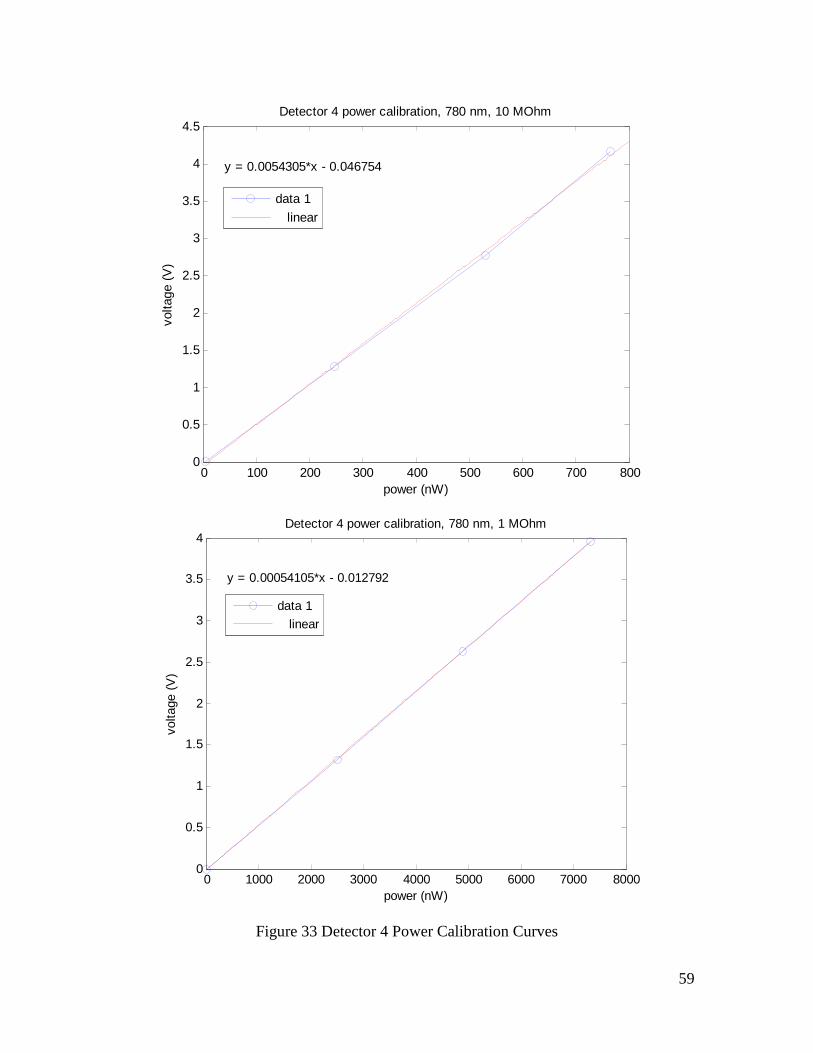
59
0 100 200 300 400 500 600 700 8000
0.5
1
1.5
2
2.5
3
3.5
4
4.5
power (nW)
volta
ge (
V)
Detector 4 power calibration, 780 nm, 10 MOhm
y = 0.0054305*x - 0.046754
data 1
linear
0 1000 2000 3000 4000 5000 6000 7000 80000
0.5
1
1.5
2
2.5
3
3.5
4
power (nW)
volta
ge (
V)
Detector 4 power calibration, 780 nm, 1 MOhm
y = 0.00054105*x - 0.012792
data 1
linear
Figure 33 Detector 4 Power Calibration Curves

60
0 10 20 30 40 50 60 70 80 900
0.5
1
1.5
2
2.5
3
3.5
4
4.5
power (nW)
volta
ge (
V)
Detector 5 power calibration, 780 nm, 100 MOhm
y = 0.05155*x - 0.20034
data 1
linear
0 20 40 60 80 100 120 140 1600
0.5
1
1.5
2
2.5
3
3.5
4
4.5
power (nW)
volta
ge (
V)
Detector 5 power calibration, 780 nm, 50 MOhm
y = 0.026826*x - 0.10258
data 1
linear

61
0 100 200 300 400 500 600 700 8000
0.5
1
1.5
2
2.5
3
3.5
4
4.5
power (nW)
volta
ge (
V)
Detector 5 power calibration, 780 nm, 10 MOhm
y = 0.0053508*x - 0.020599
data 1
linear
0 1000 2000 3000 4000 5000 6000 7000 8000-0.5
0
0.5
1
1.5
2
2.5
3
3.5
4
4.5
power (nW)
volta
ge (
V)
Detector 5 power calibration, 780 nm, 1 MOhm
y = 0.00053475*x - 0.0027906
data 1
linear
Figure 34 Detector 5 Power Calibration Curves

62
0 10 20 30 40 50 60 70 800
0.5
1
1.5
2
2.5
3
3.5
4
4.5
power (nW)
volta
ge (
V)
Detector 6 power calibration, 780 nm, 100 MOhm
y = 0.057937*x - 0.32805
data 1
linear
0 50 100 150-0.5
0
0.5
1
1.5
2
2.5
3
3.5
4
4.5
power (nW)
volta
ge (
V)
Detector 6 power calibration, 780 nm, 50 MOhm
y = 0.029192*x - 0.1631
data 1
linear

63
0 100 200 300 400 500 600 7000
0.5
1
1.5
2
2.5
3
3.5
4
4.5
power (nW)
volta
ge (
V)
Detector 6 power calibration, 780 nm, 10 MOhm
y = 0.0059871*x + 0.00045604
data 1
linear
0 1000 2000 3000 4000 5000 6000 7000 80000
0.5
1
1.5
2
2.5
3
3.5
4
4.5
power (nW)
volta
ge (
V)
Detector 6 power calibration, 780 nm, 1 MOhm
y = 0.00056397*x + 0.027536
data 1
linear
Figure 35 Detector 6 Power Calibration Curves
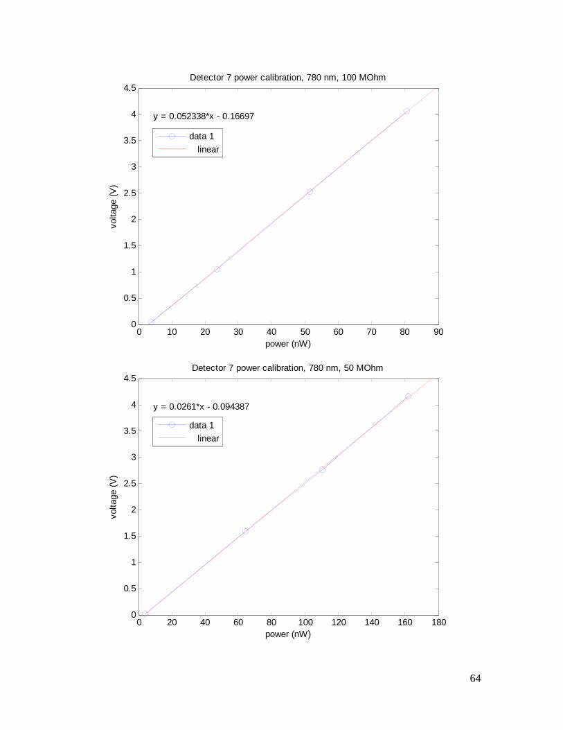
64
0 10 20 30 40 50 60 70 80 900
0.5
1
1.5
2
2.5
3
3.5
4
4.5
power (nW)
volta
ge (
V)
Detector 7 power calibration, 780 nm, 100 MOhm
y = 0.052338*x - 0.16697
data 1
linear
0 20 40 60 80 100 120 140 160 1800
0.5
1
1.5
2
2.5
3
3.5
4
4.5
power (nW)
volta
ge (
V)
Detector 7 power calibration, 780 nm, 50 MOhm
y = 0.0261*x - 0.094387
data 1
linear

65
0 100 200 300 400 500 600 700 800 9000
0.5
1
1.5
2
2.5
3
3.5
4
4.5
power (nW)
volta
ge (
V)
Detector 7 power calibration, 780 nm, 10 MOhm
y = 0.0051883*x - 0.03267
data 1
linear
0 1000 2000 3000 4000 5000 6000 7000 8000-0.5
0
0.5
1
1.5
2
2.5
3
3.5
4
4.5
power (nW)
volta
ge (
V)
Detector 7 power calibration, 780 nm, 1 MOhm
y = 0.00052458*x - 0.02945
data 1
linear
Figure 36 Detector 7 Power Calibration Curves

66
0 10 20 30 40 50 60 70 800
0.5
1
1.5
2
2.5
3
3.5
4
4.5
power (nW)
volta
ge (
V)
Detector 8 power calibration, 780 nm, 100 MOhm
y = 0.054479*x - 0.18133
data 1
linear
0 20 40 60 80 100 120 140 1600
0.5
1
1.5
2
2.5
3
3.5
4
4.5
power (nW)
volta
ge (
V)
Detector 8 power calibration, 780 nm, 50 MOhm
y = 0.027411*x - 0.10179
data 1
linear
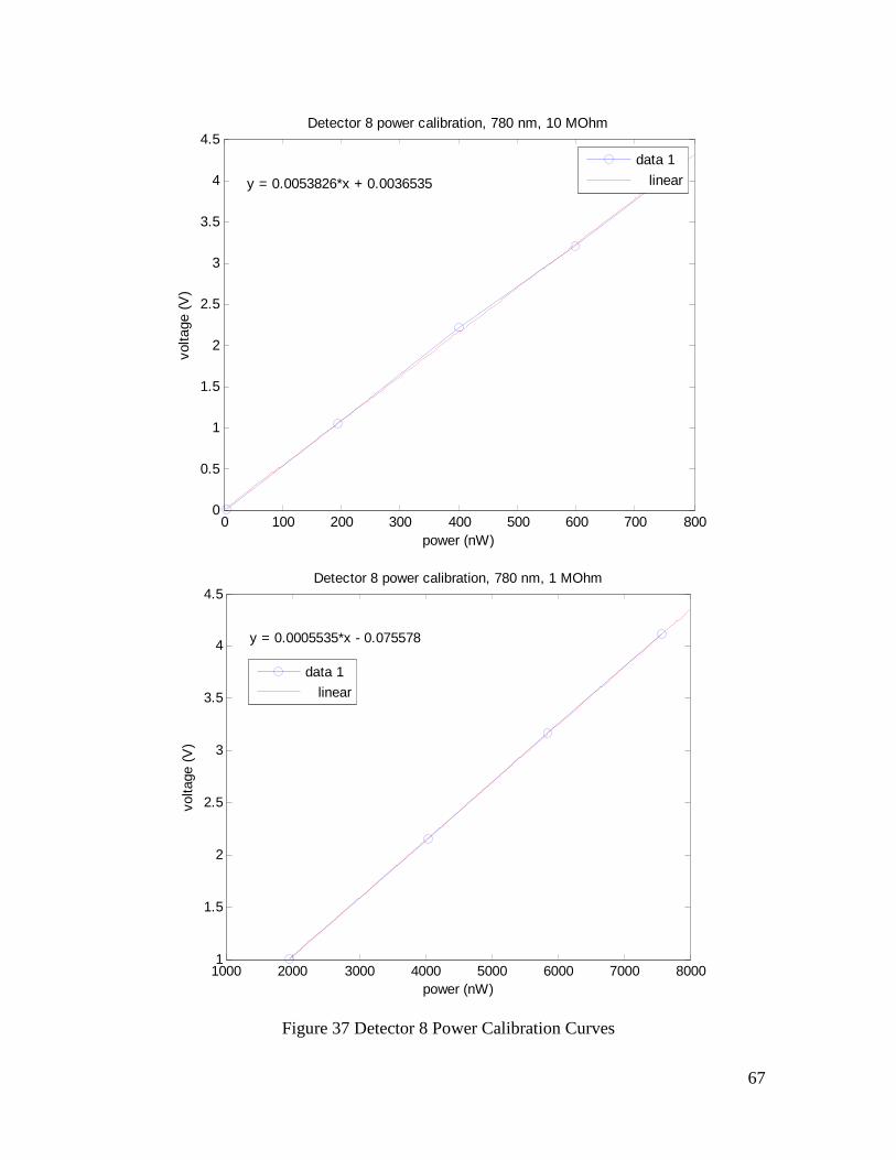
67
0 100 200 300 400 500 600 700 8000
0.5
1
1.5
2
2.5
3
3.5
4
4.5
power (nW)
volta
ge (
V)
Detector 8 power calibration, 780 nm, 10 MOhm
y = 0.0053826*x + 0.0036535
data 1
linear
1000 2000 3000 4000 5000 6000 7000 80001
1.5
2
2.5
3
3.5
4
4.5
power (nW)
volta
ge (
V)
Detector 8 power calibration, 780 nm, 1 MOhm
y = 0.0005535*x - 0.075578
data 1
linear
Figure 37 Detector 8 Power Calibration Curves

68
References
1. Graeme, Jerald. “FET op amps convert photodiode outputs to useful signals”. EDN, October 29th 1987, 205-220
2. Tony Wang, Barry Erhman. “Compensate Transimpedance Amplifiers
Intuitively”. Texas Instruments Application Report, SBOA055A, March 1993, Revised March 2005.
3. Thorlabs FDS1010 Si Photodiode datasheet. 2739-S01 Revision B. April 30th 2001.
4. Texas Instruments OPA381 OPA2381 datasheet. SBOS313B. August 2004, Revised November 2004.
5. Texas Instruments OPA656 datasheet. SBOS197B. December 2001, Revised May 2004.
6. Report titled “Photodiode Project” written by Dr. James Booth detailing his past work on the project.
7. Meetings with Dr. Kirk Madison, Dr. James Booth, and Dr. Bruce Klappauf on September 8th and September 12th 2008
8. Pease, Bob. "What’s All This Transimpedance Amplifier Stuff, Anyhow? (Part 1)”. electronic design online, January 8th 2001. <http://electronicdesign.com/Articles/Index.cfm?AD=1&ArticleID=4346 >
9. Wikipedia Magneto-Optical Trap article, September 18th 2008.
< http://en.wikipedia.org/wiki/Magneto-optical_trap>
10. Hobbs, Philip C.D. “Photodiode Front Ends: The Real Story”. Optics and Photonics News, April 2001, 44-47.
11. Ying-Cheng Chen, Yean-An Liao, Long Hsu, Ite A. Yu. “Simple technique for
measuring the number of atoms in a magneto-optical trap”. APS Physics, Revision A, Volume 64, Issue 3, August 13 2001.
12. Hobbs, Philip C.D. “Building Electro-Optical Systems: Making it all Work”.
John Wiley & Sons, Inc, 2000.
13. New Focus Visible 125 MHz photoreceiver product page, January 11th 2009. <http://www.newfocus.com/products/?navId=3&theView=modelGroupDetail&productLineId=3&productGroupId=137&modelGroupId=1054>.

69
14. Paul Horowitz, Winfield Hill. “The Art of Electronics”. Cambridge University Press, 1980.
15. Analog Devices AD8655 datasheet. D05304-0-6/05(A), Revision A. 2005.
16. Analog Devices AD8027 datasheet. C03327-0-3/05(C), Revision C. 2005.
17. Analog Devices AD8625/AD8626/AD8627 datasheet. C03023-0-11/04(C),
Revision C. 2004.
18. Analog Devices AD8221 datasheet. D03149-0-9/07(B), Revision B. 2007.
19. Texas Instruments OPA380 OPA2380 datasheet. SBOS291G. November 2003, Revised September 2007.


![Ultrafast Mechanical Shutters for Laser Cooling ...qdg/publications/InternalReports/LM-APSC479.pdf · 1.1.1. Transfer to a Magnetic Trap ... Figure 4: [wikipedia] ... Ultrafast Hard](https://static.fdocuments.us/doc/165x107/5aaf6fe77f8b9a6b308d4eb2/ultrafast-mechanical-shutters-for-laser-cooling-qdgpublicationsinternalreportslm-.jpg)


