A Low-Power Capacitive Transimpedance D/A Converter
63
Rochester Institute of Technology Rochester Institute of Technology RIT Scholar Works RIT Scholar Works Theses 12-2020 A Low-Power Capacitive Transimpedance D/A Converter A Low-Power Capacitive Transimpedance D/A Converter Sundararaman Velayutham [email protected] Follow this and additional works at: https://scholarworks.rit.edu/theses Recommended Citation Recommended Citation Velayutham, Sundararaman, "A Low-Power Capacitive Transimpedance D/A Converter" (2020). Thesis. Rochester Institute of Technology. Accessed from This Thesis is brought to you for free and open access by RIT Scholar Works. It has been accepted for inclusion in Theses by an authorized administrator of RIT Scholar Works. For more information, please contact [email protected].
Transcript of A Low-Power Capacitive Transimpedance D/A Converter

Rochester Institute of Technology Rochester Institute of Technology
RIT Scholar Works RIT Scholar Works
Theses
12-2020
A Low-Power Capacitive Transimpedance D/A Converter A Low-Power Capacitive Transimpedance D/A Converter
Sundararaman Velayutham [email protected]
Follow this and additional works at: https://scholarworks.rit.edu/theses
Recommended Citation Recommended Citation Velayutham, Sundararaman, "A Low-Power Capacitive Transimpedance D/A Converter" (2020). Thesis. Rochester Institute of Technology. Accessed from
This Thesis is brought to you for free and open access by RIT Scholar Works. It has been accepted for inclusion in Theses by an authorized administrator of RIT Scholar Works. For more information, please contact [email protected].
A Low-Power Capacitive Transimpedance D/A Converter
by
Sundararaman Velayutham
A Thesis Submitted in Partial Fulfillment of the
Requirements for the Degree of
Master of Science
in
Electrical Engineering
Approved by:
_________________________________________________
Advisor: Dr. James E. Moon
_________________________________________________
Co-Advisor: Dr. Mark Pude
_________________________________________________
Member: Dr. P R Mukund
_________________________________________________
Department Head: Dr. Ferat Sahin
Department of Electrical and Microelectronic Engineering
Kate Gleason College of Engineering
Rochester Institute of Technology
Rochester, New York
December 2020

THESIS RELEASE PERMISSION
Department of Electrical and Microelectronic Engineering
Kate Gleason College of Engineering
Rochester Institute of Technology
Rochester, New York
Title of Thesis:
A Low-Power Capacitive Transimpedance D/A Converter
I, Sundararaman Velayutham, hereby grant permission to Wallace Memorial Library of the
Rochester Institute of Technology to reproduce my thesis in whole or in part. Any
reproduction will not be for commercial use or profit.
Signature _______________________________________________________________
Date

ACKNOWLEDGEMENT This thesis would not have been possible without the support of many individuals who
I would like to thank here.
I would like to thank my advisor Dr. James E. Moon, for placing confidence in me and
accepting to be the advisor for my thesis. His guidance, teaching methodology and work ethic
has always inspired to me to become better and strive for consistency. His attention to detail is
unparalleled, and it would not have been possible to come up with this thesis report without his
patient, valuable and detailed feedback.
I would like to thank my professor/manager Dr. Mark Pude for his valuable guidance
throughout my thesis. I am really grateful to him for making time apart from his work hours to
address my questions and doubts whenever in need. I have worked with him for almost two
years now and he has always been an inspiration to me in the field of IC design.
The start to my journey in Analog IC design was from my professor Dr. P R Mukund
who has taught me the fundamentals so well, with which I was able to learn and chose this field
to pursue my career. His advice off the class about life as a whole, has been really valuable and
something that I would carry with me as I move forward in life.
Another important person I have to thank is Eric Bohannon for giving me this idea to
work on for my master’s thesis which would not have initiated without him. I would also like
to thank Eric Moule and Wayne Mao who guided me so well and patiently during my internship
at Sony and gave me the skills that helped a great deal in carrying out my thesis design. I thank
my friend Ryan Tatu for taking his time to help me fix and point out issues in my designs.
Finally, I can never thank my parents Dr. G. Velayutham and Dr. V. Rajalakshmi
enough for believing in me and creating this opportunity for me without which none of this
would have been possible. The support and love of my parents and fiancée Dr. N. Jyotsna has
helped me a great deal to reach the finish line.

ABSTRACT
This thesis proposes a new low-power and low-area DAC for single-slope ADCs used
in CMOS image sensors. With increase in resolution requirements for ADCs, conventional
DAC architectures suffered the limitation of either large area or high power consumption with
higher resolution scaling. Thus, the proposed capacitive transimpedance amplifier DAC (CTIA
DAC) could solve this by offering the resolution requirement required without taking a hit on
the area or power budget. The thesis has been structured in the following manner:
The first chapter introduces image sensors in general and talks about progression
through different image sensors and pixel architectures that have been used through the years.
It also explains the operation of a CMOS image sensor from a paper published from Sony on
high-speed image sensors.
The second chapter presents the importance and role of DACs in CMOS image sensors
and briefly explains a few commonly used DAC architectures in image sensors. It explains the
advantages and disadvantages of present architectures and leads the discussion towards the
development of the proposed DAC.
The third chapter gives an overview of the CTIA DAC and explains the working of the
different circuit blocks that are used to implement the proposed DAC.
Chapter Four explains the design approach for the blocks explained in Chapter Three.
It presents the critical design choices that were made for overall performance of the DAC.
Results of individual blocks and the DAC as a whole are presented and compared against other
recently published DAC papers.
The final chapter summarizes some key results of the design and talks about the scope
for future work and improvement.

Contents
1 INTRODUCTION ......................................................................................................................................... 1
1.1 CCD Image Sensors .............................................................................................................................. 1
1.1.1 Frame Transfer CCD (FT-CCD) .................................................................................................. 2
1.1.2 Full-Frame Transfer (FFT-CCD).................................................................................................. 3
1.1.3 Interline Transfer CCD (ILT-CCD) ............................................................................................. 3
1.2 CMOS Image Sensors ........................................................................................................................... 4
1.2.1 Passive Pixel Structure ................................................................................................................. 5
1.2.2 Active Pixel Sensors ..................................................................................................................... 6
1.3 Operation of a CMOS Image Sensor. .................................................................................................... 8
1.4 A/D Converters in CIS ........................................................................................................................ 10
2 DIGITAL-TO-ANALOG CONVERTERS IN CIS ..................................................................................... 12
2.1 Flash Resistive DAC ........................................................................................................................... 12
2.2 Capacitive DAC .................................................................................................................................. 13
2.3 Current-Steering DAC ........................................................................................................................ 14
3 CAPACITIVE TRANSIMPEDANCE AMPLIFIER DAC ......................................................................... 16
3.1 Overview ............................................................................................................................................. 16
3.2 Rail-to-Rail Amplifier ......................................................................................................................... 18
3.3 Biasing Circuit – Sooch Cascode Current Mirror ............................................................................... 21
3.4 Current Regulator ................................................................................................................................ 23
3.5 Banba Bandgap Reference .................................................................................................................. 25
3.6 Analog Switch and Multiplexer .......................................................................................................... 29
4 DESIGN APPROACH AND RESULTS ..................................................................................................... 31
4.1 gm/Id Design Methodology ................................................................................................................ 31
4.2 Rail to Rail Amplifier Design ............................................................................................................. 35
4.2.1 Biasing Circuit ............................................................................................................................ 35
4.2.2 Amplifier .................................................................................................................................... 36
4.2.3 Results ........................................................................................................................................ 37
4.3 Two-Stage Amplifier Design .............................................................................................................. 39
4.3.1 Results ........................................................................................................................................ 39
4.4 Current Regulator Design ................................................................................................................... 41
4.4.1 Results ........................................................................................................................................ 42
4.5 Banba Bandgap Reference Design ...................................................................................................... 45
4.5.1 Results ........................................................................................................................................ 46
4.6 Integrator Design (Noise Analysis for Cfb) .......................................................................................... 49
4.7 Full Test Bench and Results ................................................................................................................ 50
5 CONCLUSION AND FUTURE WORK..................................................................................................... 54
REFERENCES ..................................................................................................................................................... 55

1
1 INTRODUCTION The evolution of solid-state image sensors changed the way and ease of photography
compared to film cameras, bringing an end to the long dominant years of film photography.
The two main types of metal-oxide-semiconductor (MOS) technology-based digital image
sensors are charge-coupled device image sensors (CCD-IS) and CMOS image sensors (CIS).
CCD-IS use MOS capacitors as their fundamental unit while CIS make use of MOSFET
amplifiers along with MOS capacitors in their fundamental unit. CIS are used in compact
devices due to low power consumption and their ability to integrate on a chip due to their same
manufacturing processes as other components. CIS had been trailing CCD-IS in performance
till the early 2010s when CIS became the more efficient image sensor of the two. They were
considered more efficient for having the better performance-to-power ratio. This brought an
end to the use of CCD-IS in commercial and consumer electronic devices. Despite the widely
different variety of applications, both CIS and CCD-IS systems have the same basic
components such as lens, filter, photodiode, readout circuit, timing control and driving circuits
for the sensor, signal processor, analog-to-digital convertor and interface electronics [1].
1.1 CCD Image Sensors CCD-IS are still being extensively used in high-performance, high-quality scientific and
industrial applications. The series of MOS capacitors in a CCD-IS have their gates biased by
low or high digital pulses [2]. Individual potential wells are formed under the gates biased at
high potential. In a two-dimensional CCD array, a portion of the gates are biased at high DC
level and the remaining gates are biased low. Charges generated by incident photons are
collected in the array of isolated potential wells. The transfer of charges in CCDs depend on
the architecture of the image sensor. The most common CCD-IS architectures are frame
transfer, full-frame transfer, and interline architectures.

2
1.1.1 Frame Transfer CCD (FT-CCD)
The FT-CCD image sensor has two separate sections. One is photosensitive while the
other is covered with an opaque material like aluminum to prevent light from entering that
region. The non-photosensitive section is of the same size as the photosensitive area and is used
as the storage section [3]. There are two vertical shift registers, one for each section, and one
horizontal shift register for the transfer mechanism. Incident photons create charges in the
photosensitive area during an exposure time. The charges are then transferred at high speed
into the storage area where the serial register reads data out one by one. During the read-out
process, the image array is integrating charge for the next frame. This architecture allows faster
frame rates because of its transfer mechanism but suffers from smearing due to over exposure
during vertical shift. The FT-CCD architecture is shown in Figure 1.
Figure 1 Frame Transfer CCD [3]
3
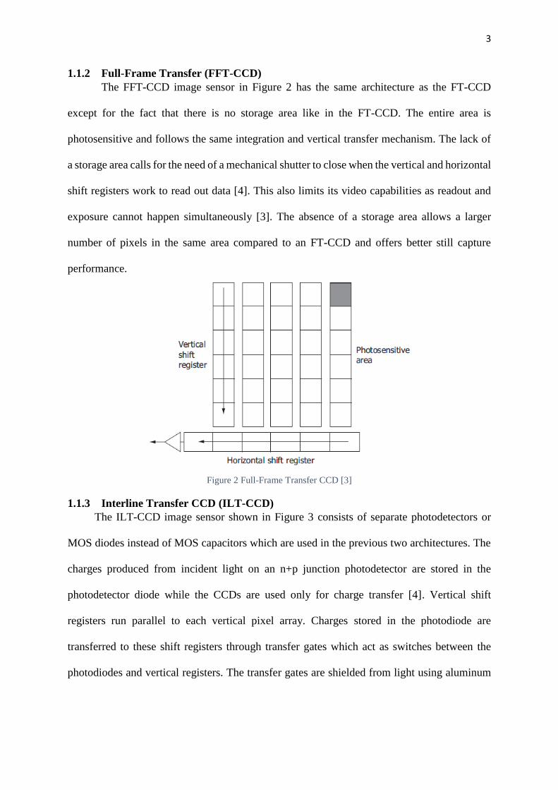
1.1.2 Full-Frame Transfer (FFT-CCD)
The FFT-CCD image sensor in Figure 2 has the same architecture as the FT-CCD
except for the fact that there is no storage area like in the FT-CCD. The entire area is
photosensitive and follows the same integration and vertical transfer mechanism. The lack of
a storage area calls for the need of a mechanical shutter to close when the vertical and horizontal
shift registers work to read out data [4]. This also limits its video capabilities as readout and
exposure cannot happen simultaneously [3]. The absence of a storage area allows a larger
number of pixels in the same area compared to an FT-CCD and offers better still capture
performance.
1.1.3 Interline Transfer CCD (ILT-CCD)
The ILT-CCD image sensor shown in Figure 3 consists of separate photodetectors or
MOS diodes instead of MOS capacitors which are used in the previous two architectures. The
charges produced from incident light on an n+p junction photodetector are stored in the
photodetector diode while the CCDs are used only for charge transfer [4]. Vertical shift
registers run parallel to each vertical pixel array. Charges stored in the photodiode are
transferred to these shift registers through transfer gates which act as switches between the
photodiodes and vertical registers. The transfer gates are shielded from light using aluminum
Figure 2 Full-Frame Transfer CCD [3]

4
[3]. This architecture was suitable for video due to the much lower smear compared to full-
frame CCDs achieved from using a separate light detecting element.
1.2 CMOS Image Sensors Though early MOS image sensors had been in existence and studied even before CCD
image sensors, temporal noise, and fixed pattern noise (FPN) were two issues that led to the
dominance of CCD-IS over CIS [1]. Shot noise and dark current come from photodiodes due
to random generation of electrons during exposure and from leakage of electrons during times
of no illumination, respectively. This noise is also seen in CCD-IS that use photodiodes.
However, in CIS, thermal noise and 1/f noise from MOS circuitry in each pixel contributes to
the additional temporal noise over CCD-IS. FPN comes from spatial variation in pixel output
under uniform illumination. CIS have higher FPN than CCD-IS because of the use of more
MOS circuitry in each pixel leading to more mismatches between pixels. The use of more than
one amplifier in CIS also leads to mismatch in gain and offset between amplifiers which also
contributes to FPN [5]. In comparison, FPN in CCD-IS only occurs from variation in
photodetector device parameter. However, CIS has the advantage of integrating circuits within
the pixel array to reduce cost and space. With different pixel architectures and techniques to
Figure 3 Interline Transfer CCD [3]
5
reduce noise, CIS became the more efficient image sensor with low cost, low power, and
similar performance [1].
Pixel architectures in CMOS image sensors are classified as passive pixel structures
(PPS) and active pixel structures (APS). The role of these circuits is to transfer photonic
information from the photodiode to the vertical column bus.
1.2.1 Passive Pixel Structure
The photodiode-type passive pixel structure was one of the first structures of the CMOS
image sensor proposed by Weckler in 1967 [6 in 1]. It is a simple structure which consists of a
photodiode with a pass transistor to transfer charges to the vertical bus. The vertical bus has a
charge integrating amplifier that integrates the generated charge. The schematic is as shown in
Figure 4.
The reset phase sets the voltage VREF on the cathodes of all photodiodes at once by
selecting all rows at once. After illumination, the generated charges are read out row-wise and
integrated across CF of the amplifier.
This architecture has a high fill factor compared to other CIS pixel architectures since
only one pass transistor is included in each pixel. However, passive pixel sensors have high
readout noise in the form of kT/C from the reset switch and CF and charge injection from the
reset switch. Scalability is also an issue due to large column bus capacitance which would
Figure 4 Simplified Passive Pixel Sensor [6]
6
reduce transfer times [1]. These issues gave CCD-IS the clear advantage over CIS until the
development of active pixel sensors.
1.2.2 Active Pixel Sensors
Active pixel sensors (APS) overcome the noise issues of passive pixel sensors by
simply using a buffer/amplifier in each pixel to isolate the pixel from the readout circuit. This
not only improves noise performance but also improves speed by using an individual amplifier
locally for each pixel. This is implemented at the cost of lower fill factor but improved signal-
to-noise ratio (SNR) overall. These improvements helped CIS close the gap on CCD-IS. Two
most common active pixel sensor structures are 3T and 4T pixel.
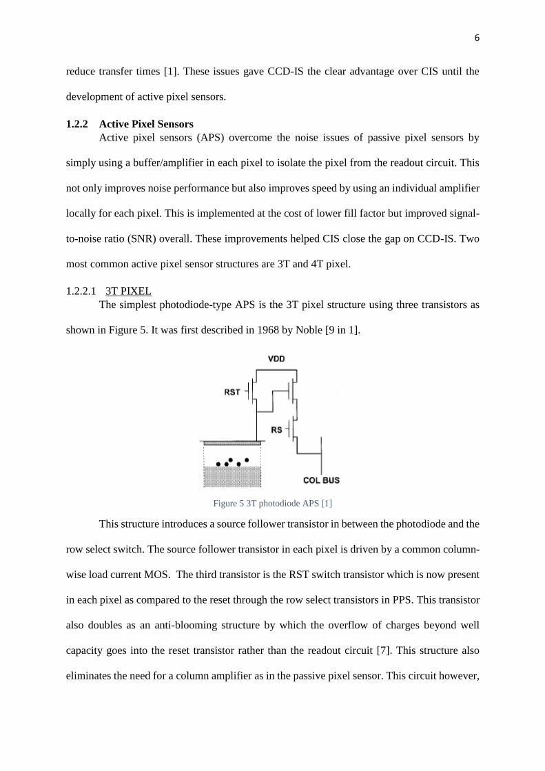
1.2.2.1 3T PIXEL
The simplest photodiode-type APS is the 3T pixel structure using three transistors as
shown in Figure 5. It was first described in 1968 by Noble [9 in 1].
This structure introduces a source follower transistor in between the photodiode and the
row select switch. The source follower transistor in each pixel is driven by a common column-
wise load current MOS. The third transistor is the RST switch transistor which is now present
in each pixel as compared to the reset through the row select transistors in PPS. This transistor
also doubles as an anti-blooming structure by which the overflow of charges beyond well
capacity goes into the reset transistor rather than the readout circuit [7]. This structure also
eliminates the need for a column amplifier as in the passive pixel sensor. This circuit however,
Figure 5 3T photodiode APS [1]
7
still has kT/C noise which couples into the readout node from the RST switch. This issue is
addressed in the 4T pixel structure.
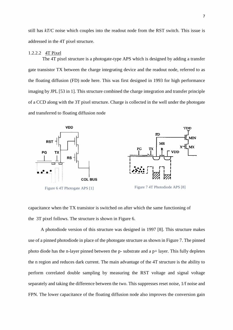
1.2.2.2 4T Pixel
The 4T pixel structure is a photogate-type APS which is designed by adding a transfer
gate transistor TX between the charge integrating device and the readout node, referred to as
the floating diffusion (FD) node here. This was first designed in 1993 for high performance
imaging by JPL [53 in 1]. This structure combined the charge integration and transfer principle
of a CCD along with the 3T pixel structure. Charge is collected in the well under the photogate
and transferred to floating diffusion node
capacitance when the TX transistor is switched on after which the same functioning of
the 3T pixel follows. The structure is shown in Figure 6.
A photodiode version of this structure was designed in 1997 [8]. This structure makes
use of a pinned photodiode in place of the photogate structure as shown in Figure 7. The pinned
photo diode has the n-layer pinned between the p- substrate and a p+ layer. This fully depletes
the n region and reduces dark current. The main advantage of the 4T structure is the ability to
perform correlated double sampling by measuring the RST voltage and signal voltage
separately and taking the difference between the two. This suppresses reset noise, 1/f noise and
FPN. The lower capacitance of the floating diffusion node also improves the conversion gain
Figure 6 4T Photogate APS [1] Figure 7 4T Photodiode APS [8]

8
(Qsig/C). Lower fill factor and complicated, expensive manufacturing process are the
disadvantages of this architecture [7].
1.3 Operation of a CMOS Image Sensor. CMOS image sensors which were compact and more power-efficient than CCD image
sensors first surpassed, then replaced CCD image sensors in the area of high-speed imaging [9]
The column parallel readout capabilities of CIS gave it the natural advantage over CCD-IS in
this area. Additionally, smearing and blooming which are problems in high-speed CCD-IS are
not noticeable in CIS. The operation of a high-speed CIS designed in [10] is explained in this
section. Figure 8 represents the block diagram of the entire CIS system.
The main parts of the CIS are 1) pixel array; 2)row decoders/drivers; 3)column parallel
ADCs; 4) a ramp generator with n-bit accuracy for the n-bit column ADCs; 5) n-bit LVDS
interface. A master clock operates the PLL and controller in the CIS, while a higher frequency
clock generated by the PLL operates the column ADCs, ramp DAC and LVDS interface. A
block diagram of the CIS is shown in Figure 8. In the conventional 4T pixel, three control
signals ΦT, ΦR, ΦS are required for its operation. These signals are controlled by the row decoder
block.
Figure 8 Block diagram of the whole system [10]

9
The column ADCs have parallel blocks of comparators and counters. The comparators
are driven by the pixel outputs and the common ramp generator circuit. The output of the
comparator is connected to the counters. The counters perform A/D conversion by counting
the clocks it takes for the ramp to cross the pixel signal level and trip the comparator.
Ripple counters are mostly used for this purpose as they are asynchronous counters that
do not need to sync with high-speed clocks. Digital CDS is performed at the counter by down
counting during the reset phase and up counting during the signal phase. Subtracting the two
signals would correct A/D conversion errors coming from clock skew, comparator delay and
counter delay. Auto-zeroing of the comparator cancels offset error and kT/C noise. The dual
CDS architecture is shown in Figure 9.
The CIS goes through the following operating sequence as shown in Figure 10. 1) A row
of pixels is selected and reset using ΦS, ΦR, and stored at capacitor C1 of the comparator. 2)
The signal ΦAZ performs auto-zero of the comparator to cancel offset and noise. 3) The
comparator changes output once ΦAZ goes low and starts the down count which stops when the
ramp signal reaches the signal level at the other input. During this period, the photodiode
integrates the signal. 4) ΦT is goes high to transfer the accumulated charges to the floating
diffusion node which is reflected as voltage at the pixel output line. The counter is also set in
Figure 9 Dual CDS architecture [10]

10
the up count mode by ΦUD going high. 5) The up count starts when the ramp starts to go down
again and outputs the noise-free signal value by subtracting the down-counted reset value from
the signal value. The final digital value is transferred to the column latches in each counter for
horizontal transfer. This completes the conversion of one row of pixels and the same steps are
continued until all rows are read out.
1.4 A/D Converters in CIS The different ADCs that can be used in the column-parallel ADC for CIS include
successive approximation ADC (SAR), a cyclic ADC and a single-slope ADC (SS-ADC).
Large area occupied by the capacitor DAC in SAR ADC is a drawback when high resolution
ADCs are required. Though cyclic ADCs can operate at high speeds, they consume high power.
The most widely used architecture for the column parallel ADCs in CIS is the single-slope
ADC (SS-ADC). They have been mostly preferred for offering good linearity and simplicity at
an average power consumption and area. But the biggest drawback is its exponentially
increasing conversion time with increase in bit resolution. A figure of merit study taking into
consideration power, area, dynamic range, and conversion time shows that shows that SS-ADC
offers the best balance of all these characteristics [11]. This justifies the extensive use of SS-
ADCs in CIS. A critical block that affects the linearity, FPN and yield characteristics of the
Figure 10 Timing diagram for the operation sequence [10]
11
SS-ADC is the ramp generator. The ramp generator needs to have good driving capabilities
and fast settling as it drives the comparators of all the column ADCs in the CIS. Finally,
excellent linearity is required to prevent INL and DNL errors in the ADC. The next chapter
talks about the different ramp generators or DACs that can be used for the SS-ADC.

12
2 DIGITAL-TO-ANALOG CONVERTERS IN CIS Digital-to-analog convertors are an important block in ADC architectures such as flash
ADC, SAR ADC, pipeline ADC and delta sigma ADC. They are used in a feedback loop in
most architectures to compare an ideal analog signal to the sampled input signal and provide
the quantization error between the two. The final value is obtained when the ADC has output
a value corresponding to the input signal within +/- 0.5 LSB of quantization error.
In SS-ADC, ramp generators play an important role in determining linearity and static
characteristics of the ADC. The commonly used DACs are flash resistive DAC, capacitor DAC
and current-steering DACs.
2.1 Flash Resistive DAC The flash resistive DAC in [12] uses a string of resistors with parallel switches and a tail
current source as shown in Figure 11. A constant current flows through this resistor string.
The switches are closed and opened one at time by a control block to control the number
of resistor units across which Vout is connected. This approach offers guaranteed monotonicity
and has row-wise noise due to less power supply and temperature sensitivity. A buffer would
Figure 11 Flash Resistive DAC [13]
13
be required to prevent kickback noise from the comparator into the ramp output. However,
scaling of this DAC beyond ten bits is hard due to an exponential increase in resistors and
control logic circuit, thereby occupying lot of area. Another disadvantage is that its linearity
depends greatly on the matching of resistors which also prevents scaling beyond ten bits due
to increased mismatch.
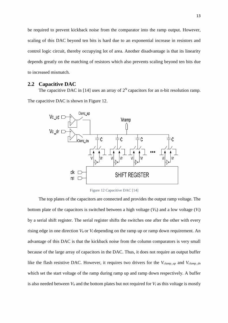
2.2 Capacitive DAC The capacitive DAC in [14] uses an array of 2N capacitors for an n-bit resolution ramp.
The capacitive DAC is shown in Figure 12.
The top plates of the capacitors are connected and provides the output ramp voltage. The
bottom plate of the capacitors is switched between a high voltage (Vh) and a low voltage (Vl)
by a serial shift register. The serial register shifts the switches one after the other with every
rising edge in one direction Vh or Vl depending on the ramp up or ramp down requirement. An
advantage of this DAC is that the kickback noise from the column comparators is very small
because of the large array of capacitors in the DAC. Thus, it does not require an output buffer
like the flash resistive DAC. However, it requires two drivers for the Vclamp_up and Vclamp_dn
which set the start voltage of the ramp during ramp up and ramp down respectively. A buffer
is also needed between Vh and the bottom plates but not required for Vl as this voltage is mostly
Figure 12 Capacitive DAC [14]
14
ground. Scaling to higher resolution is also a problem here as seen in the resistive DAC due to
the large array of capacitors added with each bit which consumes area. The drivers also would
need to be more capable of driving a larger capacitive load which would consume more power.
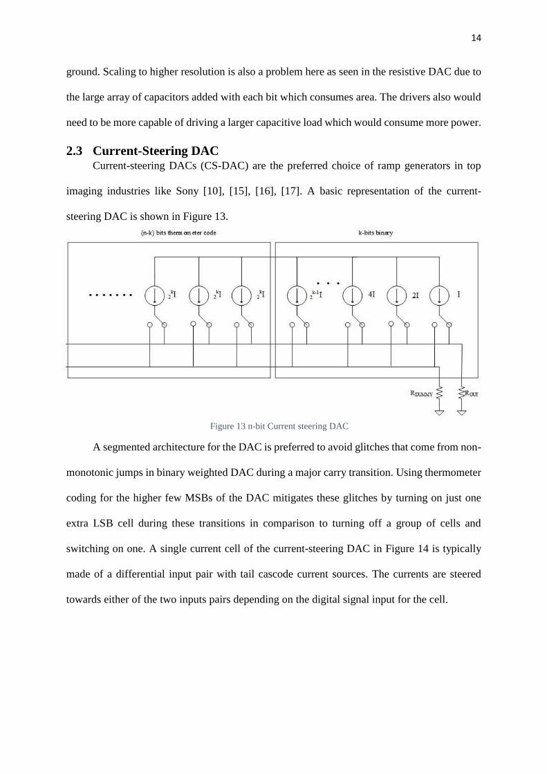
2.3 Current-Steering DAC Current-steering DACs (CS-DAC) are the preferred choice of ramp generators in top
imaging industries like Sony [10], [15], [16], [17]. A basic representation of the current-
steering DAC is shown in Figure 13.
A segmented architecture for the DAC is preferred to avoid glitches that come from non-
monotonic jumps in binary weighted DAC during a major carry transition. Using thermometer
coding for the higher few MSBs of the DAC mitigates these glitches by turning on just one
extra LSB cell during these transitions in comparison to turning off a group of cells and
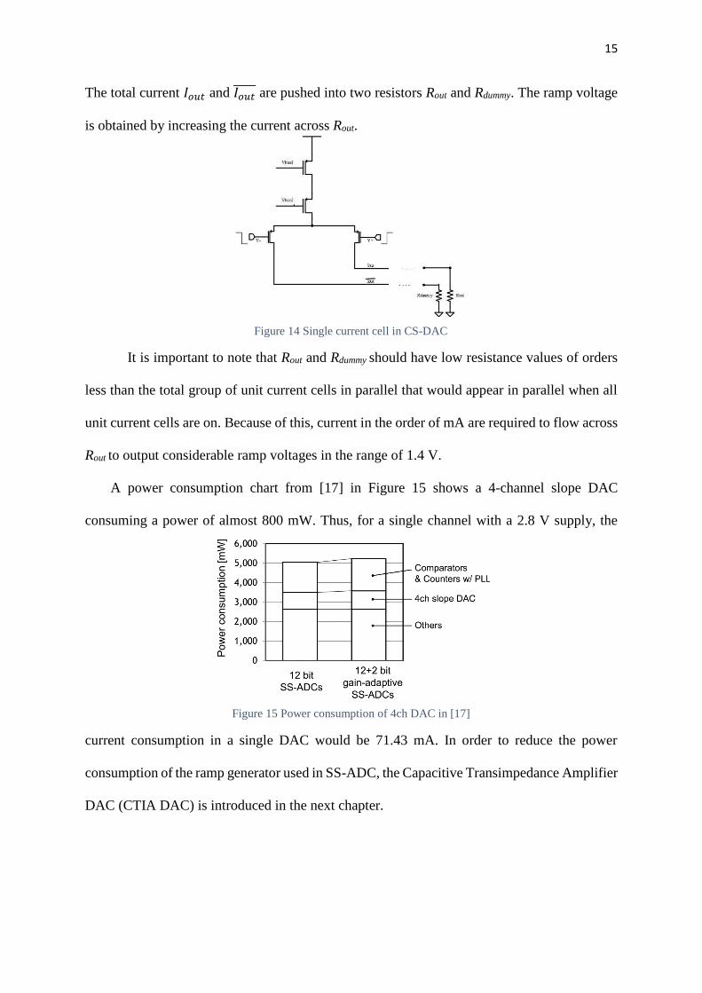
switching on one. A single current cell of the current-steering DAC in Figure 14 is typically
made of a differential input pair with tail cascode current sources. The currents are steered
towards either of the two inputs pairs depending on the digital signal input for the cell.
Figure 13 n-bit Current steering DAC
15
The total current 𝐼𝑜𝑢𝑡 and 𝐼𝑜𝑢𝑡̅̅ ̅̅ ̅ are pushed into two resistors Rout and Rdummy. The ramp voltage
is obtained by increasing the current across Rout.
It is important to note that Rout and Rdummy should have low resistance values of orders
less than the total group of unit current cells in parallel that would appear in parallel when all
unit current cells are on. Because of this, current in the order of mA are required to flow across
Rout to output considerable ramp voltages in the range of 1.4 V.
A power consumption chart from [17] in Figure 15 shows a 4-channel slope DAC
consuming a power of almost 800 mW. Thus, for a single channel with a 2.8 V supply, the
current consumption in a single DAC would be 71.43 mA. In order to reduce the power
consumption of the ramp generator used in SS-ADC, the Capacitive Transimpedance Amplifier
DAC (CTIA DAC) is introduced in the next chapter.
Figure 15 Power consumption of 4ch DAC in [17]
Figure 14 Single current cell in CS-DAC
16
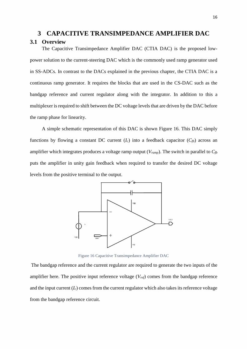
3 CAPACITIVE TRANSIMPEDANCE AMPLIFIER DAC
3.1 Overview The Capacitive Transimpedance Amplifier DAC (CTIA DAC) is the proposed low-
power solution to the current-steering DAC which is the commonly used ramp generator used
in SS-ADCs. In contrast to the DACs explained in the previous chapter, the CTIA DAC is a
continuous ramp generator. It requires the blocks that are used in the CS-DAC such as the
bandgap reference and current regulator along with the integrator. In addition to this a
multiplexer is required to shift between the DC voltage levels that are driven by the DAC before
the ramp phase for linearity.
A simple schematic representation of this DAC is shown Figure 16. This DAC simply
functions by flowing a constant DC current (Ic) into a feedback capacitor (Cfb) across an
amplifier which integrates produces a voltage ramp output (Vramp). The switch in parallel to Cfb
puts the amplifier in unity gain feedback when required to transfer the desired DC voltage
levels from the positive terminal to the output.
The bandgap reference and the current regulator are required to generate the two inputs of the
amplifier here. The positive input reference voltage (Vref) comes from the bandgap reference
and the input current (Ic) comes from the current regulator which also takes its reference voltage
from the bandgap reference circuit.
Figure 16 Capacitive Transimpedance Amplifier DAC
17
The circuit is capable of driving DC voltages that are required before the ramp phase
as a step to improve linearity. A DC voltage higher than the start voltage of the ramp, gives the
amplifier’s operating points enough time to settle before reaching the start voltage when the
feedback switch is opened. The signal from the pixel is compared to this ramp in a comparator
which trips and stops the digital counter in the SS-ADC when the ramp goes below the signal
level.
The output of the integrator during its ramp phase is given by (3.1).
𝑉𝑟𝑎𝑚𝑝 = 𝑉𝑟𝑒𝑓 −
1
𝐶𝑓𝑏∫ 𝐼𝑐 𝑑𝑡
𝑡
0
(3.1)
The slope requirement of this ramp is determined by the resolution requirement of the
ADC. For a set counter clock frequency, a high slope ramp would lead to a lower resolution
owing to a bigger voltage change between clock cycles and a low slope would give a higher
resolution because of smaller voltage steps between each clock sample. A programmable slope
can also be implemented by programming the current or having parallel capacitors in feedback
with switches.
From (3.1) the slope of the Vramp can be written as
𝑑𝑉𝑟𝑎𝑚𝑝
𝑑𝑡= −
𝐼𝑐
𝐶𝑓𝑏
(3.2)
From (3.2), it is clear that, the slope of this ramp can be set using Ic and Cfb. The feedback
capacitor in this design can be chosen by doing a noise analysis of the integrator which is shown
later in Section (4.6).

18
3.2 Rail-to-Rail Amplifier The amplifier is the main block of the integrator. The amplifier holds the input terminals
at the desired reference voltage and allows the output voltage of the integrator to decrease with
the input current through Cfb. An op-amp with a high gain and rail-to-rail output is required for
good linearity and to prevent the op amp from saturating when approaching either rail. For this
reason, a two-stage amplifier with a folded cascode first stage and a class AB output stage
architecture is chosen from [18]. The schematic of the rail-to-rail output amplifier is shown in
Figure 17.
The DC bias for the class AB output stage is obtained from the two head-to-tail connected
transistors M13 and M14. The gates of these transistors are biased by stacked diode transistors
M15, M16, M17 and M18. The translinear loops formed by M15, M16, M13, M24 and M17,
M18, M14, M23 determine the quiescent current in the output stage.
The impedance across Vg23 and Vg24 looking into M13 and M14 is given by
𝑍13,14 =
𝑉𝑔23 − 𝑉𝑔24
𝑔𝑚14𝑉𝑔23 − 𝑔𝑚13𝑉𝑔24
(3.3)
Figure 17 Rail-to-rail amplifier

19
From (3.3), it is clear that this impedance can be kept low by designing M13, M14 to have their
transconductances close to each other. It is called a floating voltage source because of its low
impedance with respect to the high impedance of the cascode stage and the gates of the output
transistors. These transistors prevent either of the output transistors from going into cutoff
when the other transistor is driven strongly. Another highlight of this implementation is that it
uses the same bias current as that of the folded cascode summing circuit to generate the dc
voltage for the output stage. A separate bias network for this control would contribute to extra
noise and offset. Because of the simple two-stage topology, Miller compensation is sufficient
to stabilize the amplifier. In this design indirect Miller compensation is done to stabilize the
amplifier with a lower capacitor. This saves some area on the chip.
The small-signal model of the differential half-circuit is shown in Figure 18. The compensation
capacitance Cc in the model represents CC2, which is the compensation capacitor in the
considered half-circuit and is always designed equal to CC1.
𝑅𝐴 = 𝑟𝑜1||𝑟𝑜4 (3.4)
𝑅2 = 𝑟𝑜24||𝑟𝑜25 (3.5)
𝑅𝑡𝑜𝑝 = 𝑟𝑜8(1 + 𝑔𝑚8𝑟𝑜10) (3.6)
𝐶𝐴 = 𝐶𝑑𝑏1 + 𝐶𝑑𝑏4 + 𝐶𝑔𝑠6 (3.7)
𝐶𝐵 = 𝐶𝑑𝑏8 + 𝐶𝑑𝑏6 + 𝐶𝑔𝑠25 (3.8)
Figure 18 Small-signal model of the rail-to-rail amplifier

20
Applying nodal analysis on the model in Figure 18 gives us the following equations.
𝑔𝑚1𝑣𝑖 +
𝑉𝐴
𝑅𝐴+ 𝑉𝐴𝑠𝐶𝐴 +
𝑉𝐴
𝑟𝑜6+ 𝑔𝑚6𝑉𝐴 −
𝑉1
𝑟𝑜6+ 𝑉𝐴𝑠𝐶𝑐 + − 𝑉𝑜𝑠𝐶𝑐 = 0
(3.9)
𝑉1
𝑅𝑡𝑜𝑝−
𝑉𝐴
𝑟𝑜6− 𝑔𝑚6𝑉𝐴 +
𝑉1
𝑟𝑜6 + 𝑉1𝑠𝐶𝐵 = 0
(3.10)
𝑉𝑜𝑠𝐶𝑐 +
𝑉𝑜
𝑅2 + 𝑉𝑜𝑠𝐶2 − 𝑉𝐴𝑠𝐶𝑐 + 𝑔𝑚2𝑉1 = 0
(3.11)
Solving these equations simultaneously gives the following transfer function.
𝑉𝑜
𝑉𝑖= (
𝑎𝑜 + 𝑎1𝑠 + 𝑎2𝑠2
𝑏𝑜 + 𝑏1𝑠 + 𝑏2𝑠2 + 𝑏3𝑠3)
(3.12)
The transfer function coefficients are:
𝑎𝑜 = 𝑔𝑚1𝑔𝑚2𝑔𝑚6𝑅𝑡𝑜𝑝𝑅𝐴𝑅2𝑟𝑜6 (3.13)
𝑎1 = −𝑔𝑚1𝑅𝐴𝑅2(𝑅𝑡𝑜𝑝 + 𝑟𝑜6)𝐶𝑐 ≈ −𝑔𝑚1𝑅𝐴𝑅2𝑅𝑡𝑜𝑝𝐶𝑐 (3.14)
𝑎2 = −𝑔𝑚1𝑅𝐴𝑅2𝑅𝑡𝑜𝑝𝑟𝑜6𝐶𝑐𝐶𝐵 (3.15)
𝑏𝑜 = 𝑅𝐴 + 𝑅𝑡𝑜𝑝 + 𝑟𝑜6 + 𝑔𝑚6𝑅𝐴𝑟𝑜6 ≈ 𝑔𝑚6𝑅𝐴𝑟𝑜6 (3.16)
𝑏2 = 𝑅2𝑅𝐴𝑅𝑡𝑜𝑝(𝐶2𝐶𝐴 + 𝐶2𝐶𝐵 + 𝐶2𝐶𝑐 + 𝐶𝐴𝐶𝑐 + 𝐶𝐵𝐶𝑐)
+ 𝑅2𝑅𝐴𝑟𝑜6(𝐶2𝐶𝐴 + 𝐶2𝐶𝑐 + 𝐶𝐴𝐶𝑐)
+ 𝑅2𝑅𝑡𝑜𝑝𝑟𝑜6(𝐶2𝐶𝐵 + 𝐶𝐵𝐶𝑐) + 𝑅𝐴𝑅𝑡𝑜𝑝𝑟𝑜6(𝐶𝐴𝐶𝐵 + 𝐶𝐵𝐶𝑐)
+ 𝑅𝑡𝑜𝑝𝑅𝐴𝑅2𝑟𝑜6𝑔𝑚6(𝐶2𝐶𝐵 + 𝐶𝐵𝐶𝑐)
≈ 𝑅𝑡𝑜𝑝𝑅𝐴𝑅2𝑟𝑜6𝑔𝑚6𝐶𝐵(𝐶2 + 𝐶𝑐)
(3.17)
𝑏3 = 𝑅𝑡𝑜𝑝𝑅𝐴𝑅2𝑟𝑜6(𝐶𝐴𝐶𝐵𝐶2 + 𝐶2𝐶𝑏𝐶𝑐 + 𝐶𝑎𝐶𝑏𝐶𝑐) (3.18)
From (3.12), the poles (p1, p2) and zero (z1) of the transfer function are approximately written
as,
𝒛𝟏 ≈ − 𝒂𝒐
𝒂𝟏 = −
𝒈𝒎𝟐𝒈𝒎𝟔𝒓𝒐𝟔
𝑪𝒄
(3.19)

21
For p1 >> p2, p3
𝒑𝟏 ≈ −
𝒃𝒐
𝒃𝟏 = −
𝟏
𝒈𝒎𝟐𝑹𝒕𝒐𝒑𝑹𝟐𝑪𝒄
(3.20)
𝒑𝟐 ≈ −
𝒃𝟏
𝒃𝟐 = −
𝒈𝒎𝟐𝑪𝒄
𝑪𝑩(𝑪𝟐 + 𝑪𝒄) ≈ −
𝒈𝒎𝟐𝑪𝒄
𝑪𝑩(𝑪𝑳)
(3.21)
(3.21) shows that indirect compensation pushes the second pole out by a factor of Cc/CL
compared to direct compensation. Thus, an improved phase margin can be achieved with a
smaller compensation capacitor.
3.3 Biasing Circuit – Sooch Cascode Current Mirror A biasing circuit is needed to bias the gates of the NMOS and PMOS cascode transistors
in the amplifier. The circuit in Figure 19, referred to as the Sooch cascode current mirror [19],
is used as the biasing circuit for the op amp. The advantage of using this circuit is that it biases
the gates of the cascode transistors in the current mirror at Vt + 2Vov as compared to 2Vt + 2Vov
in the case of a simple current mirror bias. This improves how low Vout can go before M2 goes
out of saturation. Additionally, using a MOSFET in triode in place of a resistor, helps to track
variations that a simple resistor is not capable of performing.
In this circuit, M6 forces M5 to operate in the triode region and drop the required voltage
of Vov across its drain and source.
The current through the bias stage is
𝐼6 =
𝑘′
2
𝑊
𝐿 6(𝑉𝐺𝑆6 − 𝑉𝑡)2
(3.22)
𝐼5 =
𝑘′
2
𝑊
𝐿 5(2(𝑉𝐺𝑆6 − 𝑉𝑡)𝑉𝐷𝑆5 − (𝑉𝐷𝑆5)2)
(3.23)
Due to the constraint imposed by M6,
𝑉𝐷𝑆5 = 𝑉𝑜𝑣 (3.24)
𝑉𝐺𝑆5 = 𝑉𝐺𝑆6 + 𝑉𝐷𝑆5 = 𝑉𝑡 + 2𝑉𝑜𝑣 (3.25)

22
With M6 in saturation,
Equating (3.22) to (3.23) and using (3.24),( 3.25)
𝑘′
2
𝑊
𝐿 6(𝑉𝑜𝑣)2 =
𝑘′
2
𝑊
𝐿 5(2(2𝑉𝑜𝑣)𝑉𝑜𝑣 − (𝑉𝑜𝑣)2)
(3.26)
Thus, the required design ratio for M5 and M6 is given by,
(
𝑾
𝑳)
𝟓=
𝟏
𝟑(
𝑾
𝑳)
𝟔
(3.27)
This gives the required voltage difference of Vov between the gates of the mirror and the cascode
transistors. This completes the schematic of the rail-to-rail amplifier.
Figure 19 Sooch cascode bias circuit

23
3.4 Current Regulator The CTIA DAC requires a robust input current for integration and bias current for the
rail-to-rail amplifier. For this purpose, a current regulator is designed as shown in Figure 20.
The circuit has an amplifier in negative feedback with a resistor and a NMOS pass element
(NMp). The error amplifier with the DC voltage (VDC) at its positive terminal forces the voltage
across R1 to be VDC and sets the required current in that branch. The output stage uses NMOS
or PMOS pass transistors depending on circuit requirements.
A PMOS pass transistor which is typically connected in a common source configuration
in this circuit would contribute to the loop gain of the regulator and also have a lower dropout
voltage requirement of just VOV compared to an NMOS. But its downside is that it’s harder to
compensate for stability. An NMOS pass transistor, on the other hand, which is connected in a
common drain configuration does not contribute to loop gain, but is easier to compensate for
stability. The usual problem of higher dropout voltage requirement coming from the output
stage of the amplifier, Vov6(OP) + Vgs(NMp) is not faced here because the op-amp is at a much
Figure 20 Current regulator
24
higher supply voltage than the drain of the NMOS pass transistor. Thus, an NMOS pass
transistor is selected here.
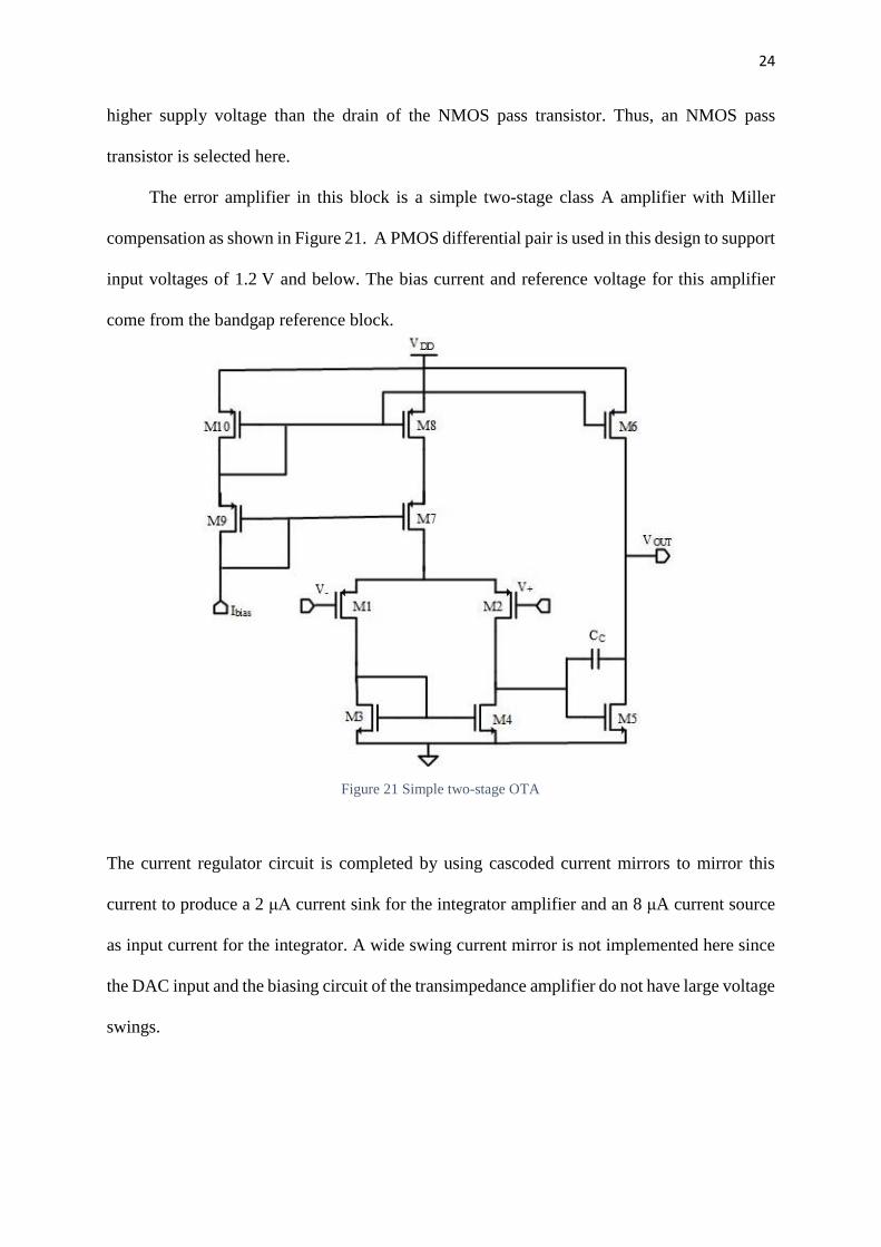
The error amplifier in this block is a simple two-stage class A amplifier with Miller
compensation as shown in Figure 21. A PMOS differential pair is used in this design to support
input voltages of 1.2 V and below. The bias current and reference voltage for this amplifier
come from the bandgap reference block.
The current regulator circuit is completed by using cascoded current mirrors to mirror this
current to produce a 2 μA current sink for the integrator amplifier and an 8 μA current source
as input current for the integrator. A wide swing current mirror is not implemented here since
the DAC input and the biasing circuit of the transimpedance amplifier do not have large voltage
swings.
Figure 21 Simple two-stage OTA

25
3.5 Banba Bandgap Reference A precise, stable and temperature-independent reference voltage is needed for the
previous two blocks in this chapter. A bias current source is also required by the two-stage
amplifiers used in the current regulator and buffer. This is accomplished on chip, using a
bandgap reference circuit [20]. These circuits output a constant voltage or current reference
that is robust against voltage and temperature variations. However, it is not robust against
process variations and often requires calibration to achieve low process variations. The
architecture used for this purpose in Figure 22 is referred to as the Banba bandgap reference
circuit.
This current-mode reference circuit generates two currents: one proportional to
temperature and the other complementary to temperature. Resistor ratios are used to control
the sensitivity of the final reference voltage obtained by forcing this current to flow through an
output resistor.
Figure 22 Bandgap reference circuit by H. Banba [20]
26
The circuit is comprised of an op-amp, resistors, diode-connected BJTs and MOSFETs. Two
BJT diodes D1 and D2 are set up in parallel branches with the area of D2 (A2) sized N times
that of D1 (A1).
The current through a diode is given by
𝐼𝐷 = 𝐼𝑠. (𝑒𝑥𝑝 (
𝑉𝑓
𝑉𝑇) − 1)
(3.28)
≅ 𝐼𝑠. 𝑒𝑥𝑝 (
𝑉𝑓
𝑉𝑇) ; 𝑉𝑓 ≫ 𝑉𝑇
(3.29)
𝑉𝑓 = 𝑉𝑇 . 𝑙𝑛 (
𝐼𝐷
𝐼𝑠)
(3.30)
Vf is complimentary to absolute temperature (CTAT) because of the stronger temperature
dependence in reverse saturation current (Is) compared to the thermal voltage (VT).
The feedback network involving the op-amp and the current mirror transistors ensures that the
same current I1 = I2 flows through both M1 and M2 in Figure 22.
Hence,
𝑉𝐴
𝑅1+ 𝐼𝐷1 =
𝑉𝐵
𝑅2+ 𝐼𝐷2
(3.31)
Since R1 = R2 and VA = VB,
𝐼𝐷1 = 𝐼𝐷2 (3.32)
Since the area A2 = N. A1,
𝐼𝐷1 ≅ 𝐼𝑠. 𝑒𝑥𝑝 (
𝑉𝑓1
𝑉𝑇)
(3.33)
𝐼𝐷2 ≅ 𝑁. 𝐼𝑠. 𝑒𝑥𝑝 (
𝑉𝑓2
𝑉𝑇)
(3.34)
Rearranging (3.33) and (3.34) for Vf1 and Vf2, and subtracting them gives,
𝛥𝑉𝑓 = 𝑉𝑓1 − 𝑉𝑓2 = 𝑉𝑇 . 𝑙𝑛(𝑁) (3.35)
where Vf1 and Vf2 are the voltages at the emitters of D1 and D2 respectively.

27
This voltage difference is proportional to absolute temperature (PTAT) due to the temperature
dependence of VT (=kT/q). This voltage drop is obtained across transistor R3 which controls
how much current flows through these diodes.
𝐼𝐷1 = 𝐼𝐷2 =
𝑉𝑇 . ln(𝑁)
𝑅3
(3.36)
Hence,
𝐼1 = 𝐼2 = 𝐼3 =
∆𝑉𝑓
𝑅3+
𝑉𝑓1
𝑅1
(3.37)
This current I3, flowing through R4 produces the required reference voltage given by
𝑉𝑟𝑒𝑓 = 𝐼3𝑅4 = 𝑅4.
∆𝑉𝑓
𝑅3+ 𝑅4.
𝑉𝑓1
𝑅1
(3.38)
In this design, the resistance R4 is split into three individual resistors to obtain three DC
voltages required by the DAC during different phases. The lowest voltage (1.1 V) is also used
as the reference voltage for the current regulator.
The op-amp designed here is the same two-stage class A amplifier as the one in the
current regulator and shown in Figure 21. The current required to bias this amplifier is obtained
by mirroring the current from M1, M2 to M4 and back into the amplifier as the bias current
through M10. This gate bias voltage from M9 is taken out of the block to be mirrored and
supply bias currents for buffers in the DAC and op-amp in the current regulator. Cascode
transistors are added to the bandgap core current mirrors to allow better mirroring of current to
the output branch which can have a different VDS across M3 depending on Vref required. Another
advantage of using cascode current mirrors is an improved PSRR performance by avoiding
coupling from the supply and the op-amp to Vref through parasitic capacitance of M3.
Startup Issue
A startup issue occurs in this circuit when the positive and negative inputs of the op-
amp (VA & VB) in the BGR are held at a zero-voltage steady state. At this state, no current flows
28
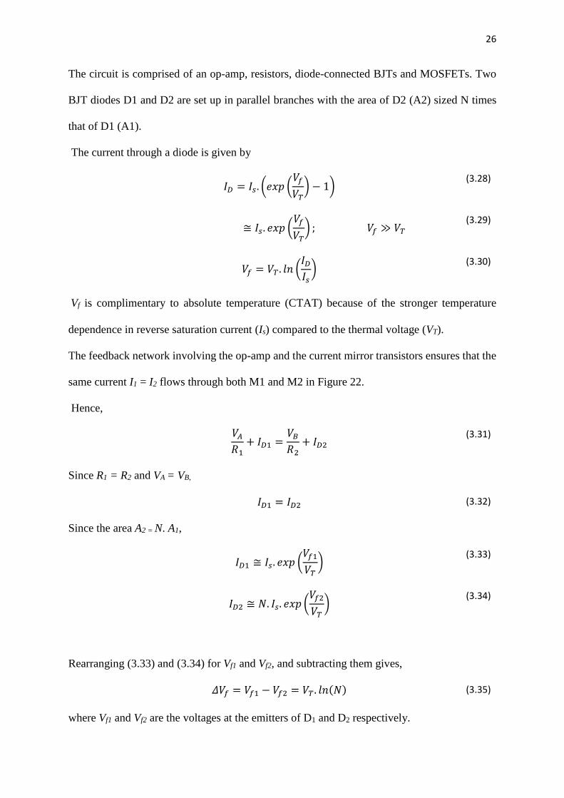
in the circuit. Hence, an external circuit is required to just move the BGR out of this undesired
steady state without affecting its operation after startup. The startup circuit is made up of a
wide PMOS MS1, a long NMOS MS2 and two more PMOS transistors MS3 and MS4 as shown
in Figure 23.
In the undesired steady state, the gates of all the PMOS and NMOS devices in the BGR
are at VDD and VSS, respectively. Since the gate of the startup circuit NMOS transistor MS2 is
connected to the gates of M1, M2, M3 and M4 which are at VDD in this undesired state, it
switches on. However, the gate of PMOS MS1 is also at VDD and wants to stays off. This moves
the drain of MS2 down to limit the current. The gates of PMOS MS3, MS4 which are driven
by this drain are switched on because of this and pull the gates of NMOS self-bias circuit (M9,
M10) and VA up. This starts the flow of current through the BGR circuit. Once all nodes are
restored to their necessary operating points, MS1 starts conducting and pulls its drain back up
which turns off MS3, MS4. This disconnects the startup circuit from the BGR after startup.
Figure 23 Startup circuit for the Bandgap Reference

29
3.6 Analog Switch and Multiplexer The analog switch required for the integrator is implemented using a transmission gate
switch as shown in Figure 24.
This switch is used instead of a NMOS- or PMOS-only switch because it offers a much
lower variation of Ron with respect to Vin as compared to a NMOS or PMOS switch. It also
cancels charge injection when sized properly. Charge injection cancellation can be achieved
by sizing the switch for a given input voltage wherever possible, by equating the channel
charges from both MOSFETs. Here we have,
𝑊𝑛. 𝐿𝑛. 𝐶𝑜𝑥(𝑉𝐷𝐷 − 𝑉𝑖𝑛 − 𝑉𝑡𝑛) = 𝑊𝑝𝐿𝑝𝐶𝑜𝑥(𝑉𝑖𝑛 − |𝑉𝑡𝑝|) (3.39)
An analog MUX is used in this DAC to switch between three different reference voltage
outputs that come from the BGR as required by the integrator before the ramp phase. The circuit
Figure 24 Transmission Gate Switch
Figure 25 Analog MUX

30
is implemented using the same transmission gate switches shown in Figure 24. The 3x1 MUX
circuit is shown in Figure 25.
The switches in the MUX are controlled by signals that determine the output of the
MUX. A buffer using the same two-stage amplifier as in the BGR and current regulator is used
at the output of the MUX to prevent the high capacitive loading that comes from the large input
transistors of the integrator.
31
4 DESIGN APPROACH AND RESULTS
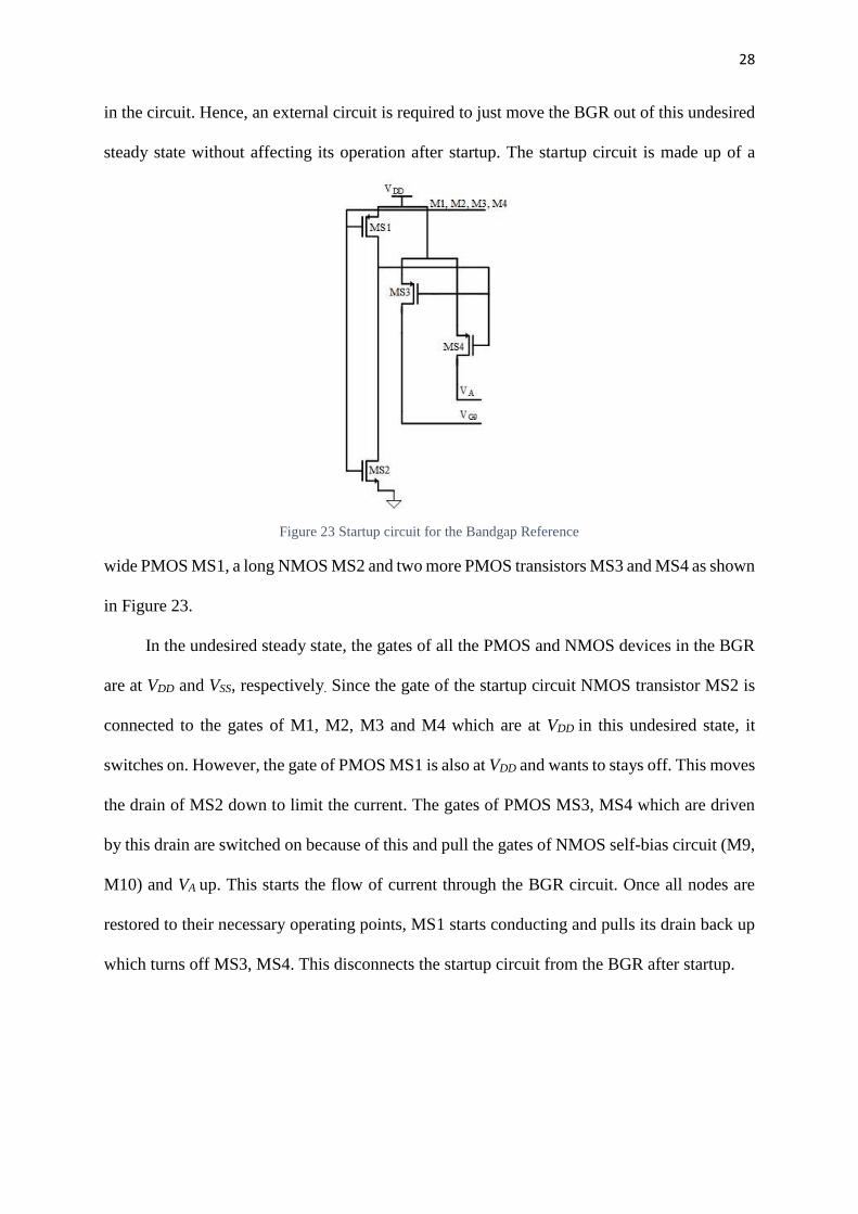
4.1 gm/Id Design Methodology The typical way of designing circuits based on strong inversion MOSFET equations and
overdrive voltage (Vov) do not hold valid when all the transistors are not in strong inversion. In
the design of any analog circuit for a given specification it is difficult to maintain strong
inversion while still keeping the transistors in saturation. This would give discrepancies to what
is expected from hand calculations.
The gm/Id methodology takes into consideration the transconductance efficiency of a
transistor, which quantifies the ability of a transistor to translate a current into an equivalent
transconductance. Studying the different intrinsic characteristics of a transistor with respect to
its gm/Id parameter allows efficient design of circuits.
𝑔𝑚
𝐼𝐷=
1
𝐼𝐷
𝜕𝐼𝐷
𝜕𝑉𝐺𝑆=
𝜕(ln 𝐼𝐷)
𝜕𝑉𝐺𝑆=
𝜕 {ln [𝐼𝐷𝑊𝐿
]}
𝜕𝑉𝐺𝑆
(4.1)
This term is maximum in weak inversion where ID has an exponential relationship with
VGS and decreases as it moves towards moderate inversion and becomes lowest in the strong
inversion region. The circuit is set up as shown in Figure 26.
Figure 26 gm/Id test circuit

32
The current density Idense (= Id/(W/L)) is swept in this circuit to obtain a gm/Id vs Idense
plot that can be divided into weak, moderate, and strong inversion regions for reference during
design. This information can be used by MOS transistors in a circuit to be sized to operate in
either of these three regions based on its function in the circuit.
In this set up, current density (Idense) is swept to study the intrinsic characteristics of the
MOSFETs in interest. Figures 27 – 29 show plots of transconductance efficiency (gm/Id), transit
frequency (ft) and intrinsic gain (gmro) of the two transistors against Idense.
Devices in weak inversion offer best transconductance efficiency at low power. Hence,
transistors that must contribute to high gain of the circuit, such as the input differential pairs of
an amplifier, can operate in this region. A low overdrive voltage is required to keep the
transistor in saturation. Hence it is useful in low-voltage designs. The disadvantage of this
region is slow speed.
Devices in strong inversion operate the fastest and provide good matching and noise
properties. Hence, current mirror transistors are biased in strong inversion. However, the gain
obtained for a given current is low and biasing all transistors in a circuit in strong inversion
would consume high power.
Moderate inversion region offers the best of both worlds by providing better voltage
gain than in strong inversion and better speed when compared to weak inversion. Hence, they
offer good all-around performance. The disadvantage is the complexity of designs in moderate
inversion, which is worth it in high-performance circuits.
A supply voltage of 2.8 V is used for all blocks in this DAC which are designed using
NMOS2V and PMOS2V devices. Hence, the intrinsic characteristics of these two transistor
models are studied.

33
Figure 28 ft vs Idense
Figure 27 gm/Id vs Idense

34
The plots in Figure 28 and Figure 29 show that a good balance of gain and speed can be
achieved in moderate inversion. Hence, most transistors in the circuits designed for this DAC
are in moderate inversion with an (ID/(W/L)) of around 1.33 μA.
Figure 29 gmro vs Idense

35
4.2 Rail to Rail Amplifier Design The amplifier used for the integrator requires high gain and high unity-gain bandwidth
for fast settling in unity-gain feedback. Rail-to-rail output swing is implemented by the use of
a class AB output stage. Since the main purpose of this thesis is to design a low-power DAC,
low power is considered in all designs.
4.2.1 Biasing Circuit
To maintain a low power consumption, a 2 μA current is used as the bias current for
this circuit to begin. Choosing this low current also makes it easy to maintain an Id/(W/L) of
around 1 μA that is required to operate all transistors in moderate inversion at a compact size.
The NMOS and PMOS Sooch cascode circuit for cascode bias is designed as shown in Figure
30. The transistors M1b, M2b, M3b, M4b form the PMOS Sooch cascode version of the circuit
in Figure 19, while transistors M7b, M8b, M9b, M10b form the NMOS Sooch cascode circuit
as shown in Figure 19. The gates of M1b, M2b and M9b, M10b bias the cascode current mirror
transistors in the amplifier.
Figure 30 Sooch cascode schematic

36
The triode transistors M2b and M7b are sized 1/3rd as that of the other transistors based
on (3.27). This biases the current mirror and cascode transistors by a small margin over the
edge of saturation.
4.2.2 Amplifier
The input transistors of the rail-to-rail amplifier are sized large for good matching, low
offset, and large transconductance. The transistors M3 and M4 in the summing circuit are sized
to be capable of sinking more than 2I1 when one of the inputs is driven high. If M3 and M4 can
sink only 2I1 or less, the transistors M4 and M5 will conduct no current during a high voltage
input step and get cut off. The output transistors of the amplifier are sized large but with small
lengths to ensure low output resistance and high speed.
The amplifier is compensated to handle a load of 30 pF to handle the large number of
comparators it would be connected to in the pixel array. The size of the compensation
capacitances (Cc1, Cc2) is determined from multiplying the dominant pole (p1) in (3.20) by the
gain to set the desired unity-gain bandwidth for fast settling. For better phase margin, Cc1, Cc2
are further increased to push the second pole (p2) in (3.21) away from the unity-gain frequency
while also reducing the dominant pole frequency. The final schematic of the rail-to-rail class
AB amplifier is as shown above in Figure 31.
Figure 31 Rail-to-rail amplifier schematic

37
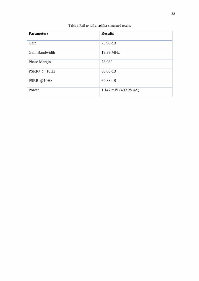
4.2.3 Results
The designed rail-to-rail amplifier is tested for stability with a load capacitance of 30
pF to take into consideration the cumulative capacitance that could come from the large number
of comparators it is connected to in the column array of an image sensor. A target gain
bandwidth specification of 12.36 MHz for the amplifier was calculated for a settling time of
100 ns within half an LSB (390 μA) for the voltage step from 1.1 V to 1.274 V in unity gain
feedback. High gain of the amplifier to hold the inputs same during integration was the priority
here over bandwidth as the bandwidth would effectively be determined by the feedback
capacitor.
The gain and phase plots in Figure 32 shows a comfortable phase margin of 73.98 ͦ. The
power supply rejection ratio (PSRR) is also tested, as supply noise could contribute to noise at
the output ramp and it is essential for the circuit to have high PSRR. PSRR+ denotes the
positive supply noise rejection while PSRR- denotes the negative supply noise rejection, both
of which are reported in Table 1.
Figure 32 Gain and phase of the rail-to-rail op-amp
38
Table 1 Rail-to-rail amplifier simulated results
Parameters Results
Gain 73.98 dB
Gain Bandwidth 19.39 MHz
Phase Margin 73.98 ͦ
PSRR+ @ 10Hz 86.08 dB
PSRR-@10Hz 69.88 dB
Power 1.147 mW (409.98 μA)
39
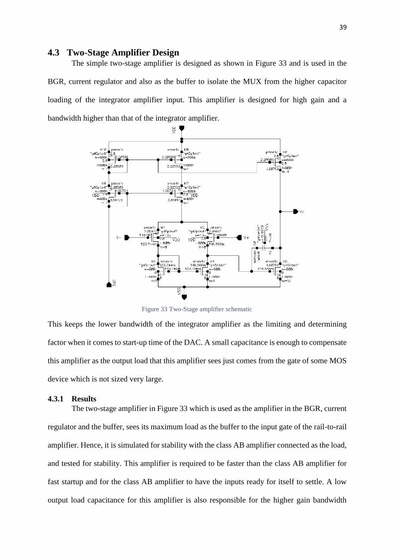
4.3 Two-Stage Amplifier Design The simple two-stage amplifier is designed as shown in Figure 33 and is used in the
BGR, current regulator and also as the buffer to isolate the MUX from the higher capacitor
loading of the integrator amplifier input. This amplifier is designed for high gain and a
bandwidth higher than that of the integrator amplifier.
This keeps the lower bandwidth of the integrator amplifier as the limiting and determining
factor when it comes to start-up time of the DAC. A small capacitance is enough to compensate
this amplifier as the output load that this amplifier sees just comes from the gate of some MOS
device which is not sized very large.
4.3.1 Results
The two-stage amplifier in Figure 33 which is used as the amplifier in the BGR, current
regulator and the buffer, sees its maximum load as the buffer to the input gate of the rail-to-rail
amplifier. Hence, it is simulated for stability with the class AB amplifier connected as the load,
and tested for stability. This amplifier is required to be faster than the class AB amplifier for
fast startup and for the class AB amplifier to have the inputs ready for itself to settle. A low
output load capacitance for this amplifier is also responsible for the higher gain bandwidth
Figure 33 Two-Stage amplifier schematic
40
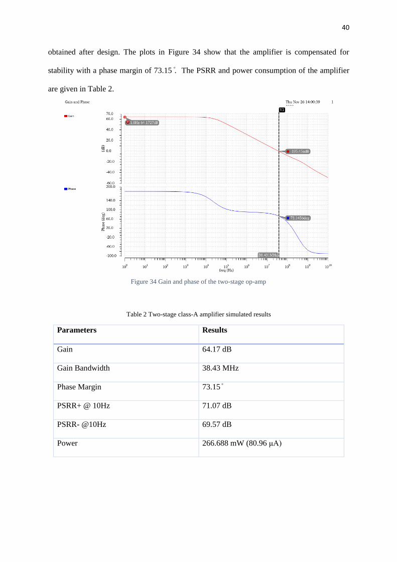
obtained after design. The plots in Figure 34 show that the amplifier is compensated for
stability with a phase margin of 73.15 ͦ. The PSRR and power consumption of the amplifier
are given in Table 2.
Table 2 Two-stage class-A amplifier simulated results
Parameters Results
Gain 64.17 dB
Gain Bandwidth 38.43 MHz
Phase Margin 73.15 ͦ
PSRR+ @ 10Hz 71.07 dB
PSRR- @10Hz 69.57 dB
Power 266.688 mW (80.96 μA)
Figure 34 Gain and phase of the two-stage op-amp

41
4.4 Current Regulator Design The objective of the current regulator is to obtain a constant current source from constant
voltage source. The output current of the regulator is given by,
𝐼𝑜𝑢𝑡 =
𝑉𝑟𝑒𝑓
𝑅
(4.2)
A Vref of 1.1 V from the BGR at the amplifier’s positive input is used along with a
550 kΩ poly-resistor at the negative input to get an Iout of 2 μA. Poly-resistor is used for R here
due to its low temperature coefficient. The NMOS pass transistor NMp does not need to be
sized large due to the low quiescent current requirement in the output branch. The
compensation of the error amplifier is sufficient for stability of the system as there is no high
capacitive load outside the amplifier to cause instability. The use of cascode current mirrors
provides a more robust and accurate mirroring of current. A switch is introduced at the gate
bias of the 8 μA current mirror transistor to have no current flowing into the CTIA DAC during
unity-gain feedback. The final schematic of the current regulator is shown in Figure 35.
Figure 35 Current Regulator design schematic
42
4.4.1 Results
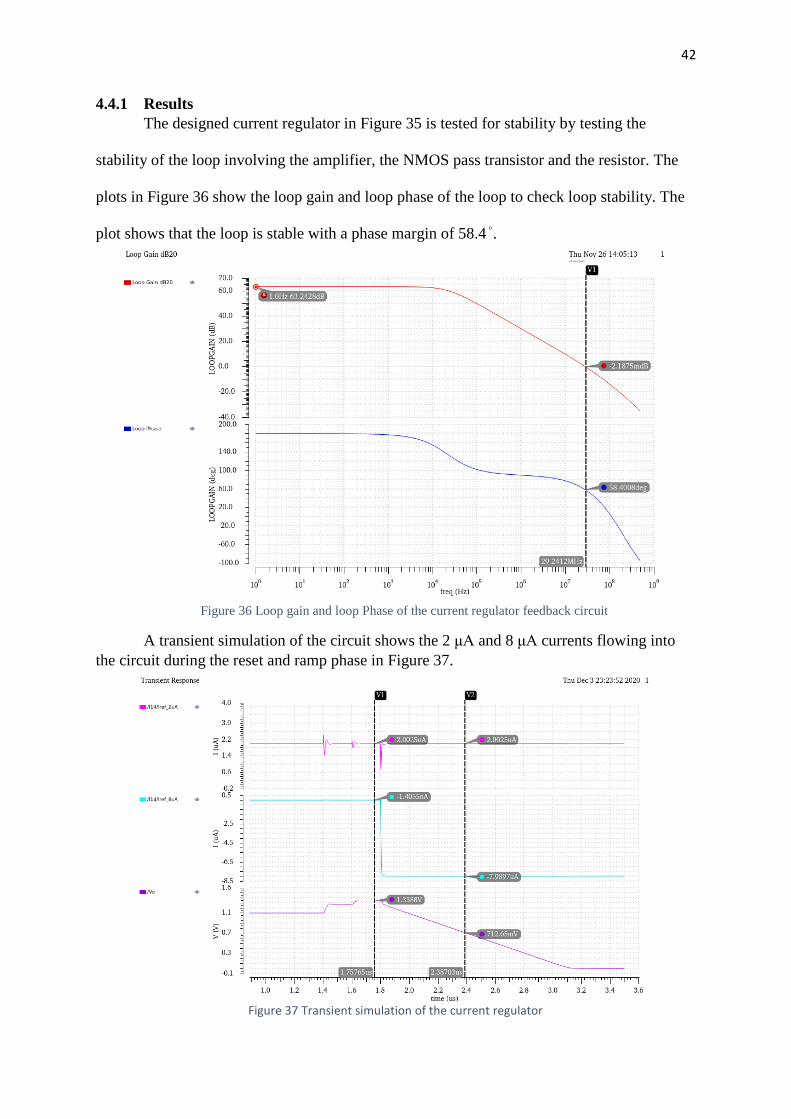
The designed current regulator in Figure 35 is tested for stability by testing the
stability of the loop involving the amplifier, the NMOS pass transistor and the resistor. The
plots in Figure 36 show the loop gain and loop phase of the loop to check loop stability. The
plot shows that the loop is stable with a phase margin of 58.4 ͦ .
A transient simulation of the circuit shows the 2 μA and 8 μA currents flowing into
the circuit during the reset and ramp phase in Figure 37.
Figure 36 Loop gain and loop Phase of the current regulator feedback circuit
Figure 37 Transient simulation of the current regulator
43
Table 3 presents simulated results such as loop gain, loop gain bandwidth and power
consumption of the current regulator.
Table 3 Current regulator simulated results
Parameters Results
LoopGain 63.24 dB
Loop GainBandwidth 29.24 MHz
Phase Margin 58.4 ͦ
Power 250.23 μW (89.268 μA)
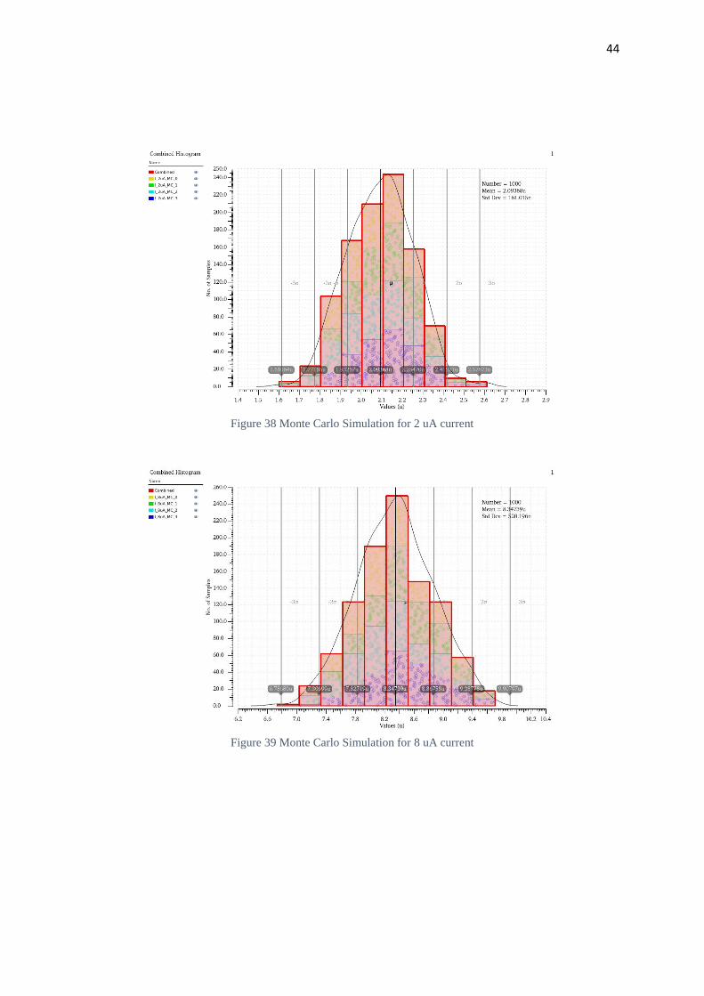
The effects of supply variation, process variation and device mismatch in this circuit is
extremely important to consider as the 8 μA current that it provides for the DAC decides the
slope of the ramp and thereby the LSB of the DAC. A 250-point Monte Carlo simulation is
done on this circuit to observe its effects on both currents at temperatures of -40 ͌C and 125 ͌C
and supply voltages of 2.6 V and 3.0 V. The two plots in Figure 38 and Figure 39 show the
mean and standard deviations of both currents. The mean value of the 2 μA current comes out
to be 2.01 μA while the mean value of the 8 μA current is 8.33 μA. Their standard deviations
are 163 nA and 507 nA, respectively. While the standard deviation of the 2 μA current is not
of great concern as it is simply the bias current for the amplifier, the 0.5 μA deviation on the 8
μA current causes significant deviation in the slope of the ramp. It important to design the
circuit to fix the mean current value to be the same as the required current for better functioning
as compared to designing to meet the requirement in typical conditions.
44
Figure 38 Monte Carlo Simulation for 2 uA current
Figure 39 Monte Carlo Simulation for 8 uA current
45
4.5 Banba Bandgap Reference Design The bandgap reference circuit is designed to attain the required reference voltages and
current bias. The complete schematic of the circuit is shown in Figure 40. The ratio of diodes
D1:D2 is chosen as 1:8 to allow a 3x3 layout array for the diodes.
Differentiating equation (3.37)
𝑑𝐼2
𝑑𝑇=
1
𝑅3
𝑑∆𝑉𝑓
𝑑𝑇+
1
𝑅1
𝑑𝑉𝑓1
𝑑𝑇
(4.3)
From equation (4.3), a ratio of R3/R1 is set to reduce the variation of I1 (=I2) with temperature.
Since the resistors also have temperature dependence, this is done by simulation. Keeping this
ratio fixed, a bias current of 8 μA required for the two stage amplifier is set to draw through
M1 and M2 by fixing R1, R2, R3. This current is mirrored to M3 and across R4 which gives VREF.
Since R4 has to be a higher resistance to obtain the required upper voltage of 1.34 V, the
variation on VREF with temperature would be larger. This now requires tweaking R1 or R3
slightly with respect to R4 to obtain a low and balanced variation of VREF across the temperature
range. In this process, the ratio set for low I1 (=I2) variation is lost. It is quite clear that only
one of the two can be achieved at a time in this architecture. The lower temperature independent
voltage reference is opted for in this case because of the need for this reference voltage by the
integrator and the current regulator. The fixed R4 value is split to obtain the three different
voltages of 1.34 V, 1.274 V and 1.1 V.
The startup circuit transistors MS1 and MS2 are sized with large width and large length
respectively to have their drain move one way or the other depending on the operating condition
of the circuit. Transistors MS3 and MS4 are sized small for easy turn on and turn off.

46
4.5.1 Results
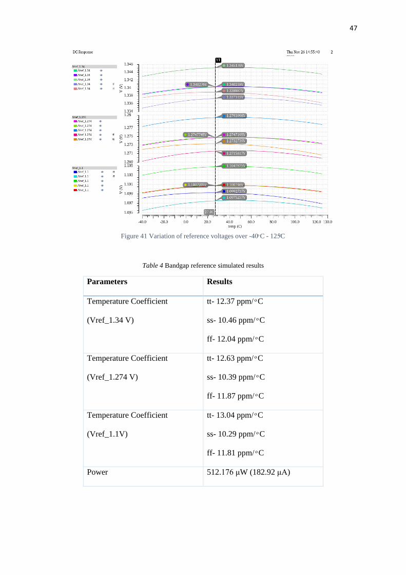
The BGR circuit in Figure 40 is tested to check the robustness of the three output
reference voltages with process and temperature. Figure 41 shows the variation of each
reference voltage with a sweep of temperature for each process corner. The temperature
coefficients of the reference voltages and the power consumption of the circuit are given in
Table 4. A Monte Carlo simulation is also performed on the circuit to test the effect of device
mismatch and process variations together on the circuit. A 250 points Monte Carlo simulation
give results as shown in Figure 42. The group of plots show the mean and standard for the
reference voltages and their temperature coefficients with device mismatch.
Figure 40 Banba bandgap voltage reference schematic
47
Table 4 Bandgap reference simulated results
Parameters Results
Temperature Coefficient
(Vref_1.34 V)
tt- 12.37 ppm/ ͦ C
ss- 10.46 ppm/ ͦ C
ff- 12.04 ppm/ ͦ C
Temperature Coefficient
(Vref_1.274 V)
tt- 12.63 ppm/ ͦ C
ss- 10.39 ppm/ ͦ C
ff- 11.87 ppm/ ͦ C
Temperature Coefficient
(Vref_1.1V)
tt- 13.04 ppm/ ͦ C
ss- 10.29 ppm/ ͦ C
ff- 11.81 ppm/ ͦ C
Power 512.176 μW (182.92 μA)
Figure 41 Variation of reference voltages over -40ͦ C - 125Cͦ
48
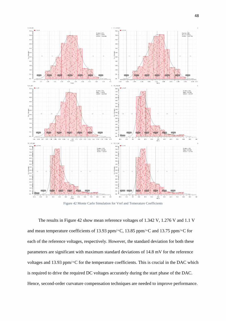
The results in Figure 42 show mean reference voltages of 1.342 V, 1.276 V and 1.1 V
and mean temperature coefficients of 13.93 ppm/ ͦ C, 13.85 ppm/ ͦ C and 13.75 ppm/ ͦ C for
each of the reference voltages, respectively. However, the standard deviation for both these
parameters are significant with maximum standard deviations of 14.8 mV for the reference
voltages and 13.93 ppm/ ͦ C for the temperature coefficients. This is crucial in the DAC which
is required to drive the required DC voltages accurately during the start phase of the DAC.
Hence, second-order curvature compensation techniques are needed to improve performance.
Figure 42 Monte Carlo Simulation for Vref and Temerature Coefficients
49
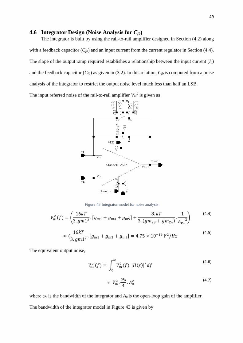
4.6 Integrator Design (Noise Analysis for Cfb) The integrator is built by using the rail-to-rail amplifier designed in Section (4.2) along
with a feedback capacitor (Cfb) and an input current from the current regulator in Section (4.4).
The slope of the output ramp required establishes a relationship between the input current (Ic)
and the feedback capacitor (Cfb) as given in (3.2). In this relation, Cfb is computed from a noise
analysis of the integrator to restrict the output noise level much less than half an LSB.
The input referred noise of the rail-to-rail amplifier Vni2 is given as
𝑉𝑛𝑖
2 (𝑓) = (16𝑘𝑇
3. 𝑔𝑚12. [𝑔𝑚1 + 𝑔𝑚3 + 𝑔𝑚9] +
8. 𝑘𝑇
3. (𝑔𝑚23 + 𝑔𝑚24).
1
𝐴𝑣12)
(4.4)
≈ (
16𝑘𝑇
3. 𝑔𝑚12. [𝑔𝑚1 + 𝑔𝑚3 + 𝑔𝑚9] = 4.75 × 10⁻¹⁶ 𝑉2/𝐻𝑧
(4.5)
The equivalent output noise,
𝑉𝑛𝑜
2 (𝑓) = ∫ 𝑉𝑛𝑖2 (𝑓). |𝐻(𝑠)|
2𝑑𝑓
∞
0
(4.6)
≈ 𝑉𝑛𝑖2 .
𝜔𝑜
4. 𝐴𝑜
2 (4.7)
where ωo is the bandwidth of the integrator and Ao is the open-loop gain of the amplifier.
The bandwidth of the integrator model in Figure 43 is given by
Figure 43 Integrator model for noise analysis

50
𝜔𝑜 =
1
𝐴𝑜 . 𝑅𝑖 . 𝐶𝑓𝑏
(4.8)
where Ri is the impedance of the input current source.
From (4.7) and (4.8),
𝑉𝑛𝑜
2 ≈ 𝑉𝑛𝑖2
𝐴𝑜
𝑅𝑖 . 𝐶𝑓𝑏= 4.75 × 10⁻¹⁶ .
5188
37.5 × 10⁶. 𝐶𝑓𝑏
(4.9)
From this relation between Cfb and Vno, the required Cfb is calculated for the maximum tolerable
output noise. This output noise is set to be 1/10th of a LSB and Cfb is calculated to be,
𝐶𝑓𝑏 =
1.643 × 10⁻¹²
6.099 × 10−9= 2.7 𝑝𝐹
(4.10)
It is also important to note that the bandgap reference and the current regulator blocks preceding
the integrator also contribute to the noise of the DAC. Hence, a larger value of 8 pF for Cfb is
chosen maintain low noise and to keep the bandwidth of the closed-loop system well within
the open-loop bandwidth (3.88 kHz) of the rail-to-rail amplifier. This completes the design of
the integrator which is tested in the next section along with other blocks.
4.7 Full Test Bench and Results
The complete test bench of the CTIA DAC with all the designed blocks connected
together is shown in Figure 44. Simulations for startup time, functionality, linearity and power
consumption are performed on this test bench.
Figure 44 Complete testbench of the CTIA DAC

51
The time it takes for the CTIA DAC to start up is shown in Figure 45. The supply VDD
is switched on at 10 ns with a rise time of 5 ns. The settling time for Vo of the DAC is measured
to be 292.2 ns.
A transient simulation is performed to test the functionality of the DAC and is shown
in Figure 46.
Figure 45 Startup time for the DAC
Figure 46 Functional verification of the DAC

52
The Integral non-linearity (INL) of the ramp is measured by using the mid-point line
method. A line is drawn through the start and mid-point points of the ramp and subtracted from
the actual ramp. This line divided by the LSB gives us the INL. This INL is shown in Figure
47.
Since the ramp here would take some time to settle from the time it is released from
unity-gain feedback, the settling point obtained from the derivative of the ramp (dVRamp/dt) is
taken as the start point for computing INL. The point on Vramp where the INL touches 0.5 LSB
is the lowest the ramp can go before moving the NMOS output transistor out of saturation.
The current consumption of each block in the DAC during operation is shown in Figure 48.
Figure 47 Integral non-linearity of the DAC
Figure 48 Individual power consumption by block
53
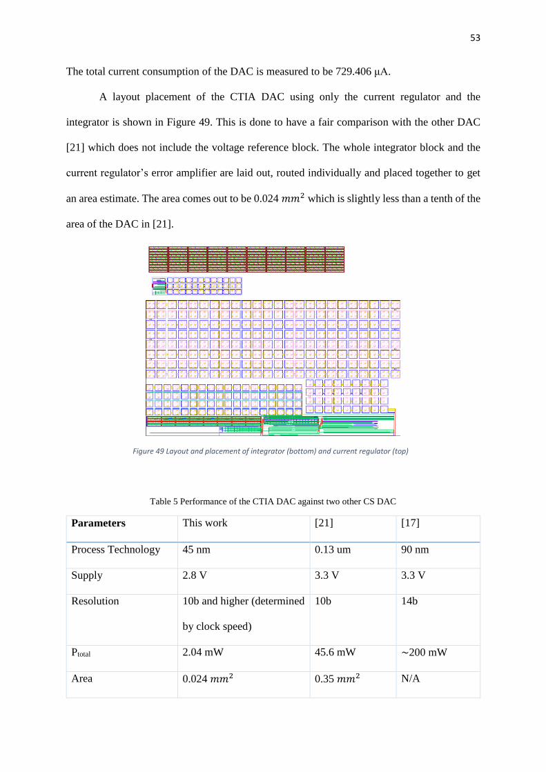
The total current consumption of the DAC is measured to be 729.406 μA.
A layout placement of the CTIA DAC using only the current regulator and the
integrator is shown in Figure 49. This is done to have a fair comparison with the other DAC
[21] which does not include the voltage reference block. The whole integrator block and the
current regulator’s error amplifier are laid out, routed individually and placed together to get
an area estimate. The area comes out to be 0.024 𝑚𝑚2 which is slightly less than a tenth of the
area of the DAC in [21].
Table 5 Performance of the CTIA DAC against two other CS DAC
Parameters This work [21] [17]
Process Technology 45 nm 0.13 um 90 nm
Supply 2.8 V 3.3 V 3.3 V
Resolution 10b and higher (determined
by clock speed)
10b 14b
Ptotal 2.04 mW 45.6 mW ~200 mW
Area 0.024 𝑚𝑚2 0.35 𝑚𝑚2 N/A
Figure 49 Layout and placement of integrator (bottom) and current regulator (top)

54
5 CONCLUSION AND FUTURE WORK In this thesis, a CTIA DAC for single-slope ADCs in image sensors is designed in a 45
nm process technology. The designed DAC operates with a 2.8 V supply and shows good
linearity for a wide voltage range up to 100 mV from either supply rail. The total power
consumption of this DAC is 2.04 mW which is much less than the commonly used current
steering DAC. It also occupies a small area, about 0.024 mm2, as compared to other DAC
architectures.
In terms of future work, the low power and low area CTIA DAC still has scope for
improvements in some areas. Programmability of the DAC by programming current or by
having capacitors in parallel with switches to control the ramp slope can be implemented. A
more robust ramp with very low process and mismatch variations can be achieved by designing
a self-calibrating circuit that calibrates the slope of the ramp to the required value before the
ramp comparison phase. This would mitigate changes in the ramp slope due to process and
mismatch induced errors that come from the bandgap reference and the current regulator.

55
REFERENCES
[1] E. R. Fossum, "CMOS image sensors: electronic camera-on-a-chip," in IEEE Transactions
on Electron Devices, vol. 44, no. 10, pp. 1689-1698, Oct. 1997, doi: 10.1109/16.628824.
[2] A. J. P. Theuwissen, "CCD or CMOS image sensors for consumer digital still
photography?," 2001 International Symposium on VLSI Technology, Systems, and
Applications. Proceedings of Technical Papers (Cat. No.01TH8517), Hsinchu, Taiwan, 2001,
pp. 168-171, doi: 10.1109/VTSA.2001.934511.
[3]Hamamatsu, “Image Sensors, Chapter 5”.
Available: https://www.hamamatsu.com/resources/pdf/ssd/e05_handbook_image_sensors.pdf
[4] E. R. Fossum and D. B. Hondongwa, "A Review of the Pinned Photodiode for CCD and
CMOS Image Sensors," in IEEE Journal of the Electron Devices Society, vol. 2, no. 3, pp. 33-
43, May 2014, doi: 10.1109/JEDS.2014.2306412.
[5] H. Tian, “Noise Analysis in CMOS image sensors,” Ph. D. dissertation, Stanford
University, United States, pp. 3-10, 2000.
[6] Tartagni, M. et al. “A Comparative Analysis of Active and Passive Pixel CMOS Image
Sensors.” (2002).
[7] Abbas El Gamal. EE 392B: CMOS Image Sensors, Chapter 4 [Online].
Available: https://isl.stanford.edu/~abbas/ee392b/lect04.pdf
[8] S. K. Mendis et al., "CMOS active pixel image sensors for highly integrated imaging
systems," in IEEE Journal of Solid-State Circuits, vol. 32, no. 2, pp. 187-197, Feb. 1997, doi:
10.1109/4.551910.

56
[9] A. I. Krymski, N. E. Bock, Nianrong Tu, D. Van Blerkom and E. R. Fossum, "A high-
speed, 240-frames/s, 4.1-Mpixel CMOS sensor," in IEEE Transactions on Electron Devices,
vol. 50, no. 1, pp. 130-135, Jan. 2003, doi: 10.1109/TED.2002.806961.
[10] Y. Nitta et al., "High-Speed Digital Double Sampling with Analog CDS on Column
Parallel ADC Architecture for Low-Noise Active Pixel Sensor," 2006 IEEE International Solid
State Circuits Conference - Digest of Technical Papers, San Francisco, CA, 2006, pp. 2024-
2031, doi: 10.1109/ISSCC.2006.1696261.
[11] M. Kwon and B. Murmann, "A New Figure of Merit Equation for Analog-to-Digital
Converters in CMOS Image Sensors," 2018 IEEE International Symposium on Circuits and
Systems (ISCAS), Florence, 2018, pp. 1-5, doi: 10.1109/ISCAS.2018.8351578.
[12] A. Laflaquiere, “Ramp generator,” US patent 6842135B2, Jan. 11, 2005. Available:
https://patents.google.com/patent/US6842135
[13] T. Bailey, “Ramp generator for image sensor ADC,” US patent 6956413, Oct. 18, 2008.
Available: https://patents.google.com/patent/US20030071666
[14] A. I. Krymski, “Ramp generation with capacitors,” US patent 6885331, Apr. 26, 2005.
Available: https://patents.google.com/patent/US6885331B2/en
[15] Shizunori Matsumoto, Chikao MIYAZAKI, “Da converter and solid-state imaging
device” US patent 8587707B2, Nov. 19, 2013
Available: https://patents.google.com/patent/US20110050967A1/en
[16] Norifumi KanagawaYasuhide Shimizu, “Digital-to-analog conversion circuit,” US patent
8836561B2, Sep. 16, 2014
Available: https://patents.google.com/patent/US8836561

57
[17] Y. Oike et al., "8.3 M-Pixel 480-fps Global-Shutter CMOS Image Sensor with Gain-
Adaptive Column ADCs and Chip-on-Chip Stacked Integration," in IEEE Journal of Solid-
State Circuits, vol. 52, no. 4, pp. 985-993, April 2017, doi: 10.1109/JSSC.2016.2639741.
[18] R. Hogervorst, J. P. Tero, R. G. H. Eschauzier and J. H. Huijsing, "A compact power-
efficient 3 V CMOS rail-to-rail input/output operational amplifier for VLSI cell libraries," in
IEEE Journal of Solid-State Circuits, vol. 29, no. 12, pp. 1505-1513, Dec. 1994, doi:
10.1109/4.340424.
[19] P. R. Gray, P. Hurst, S. Lewis, and R. G. Meyer, Analysis and Design of Analog Integrated
Circuits, 4th ed., New York, NY: Wiley, pp. 270-272, 2001.
[20] H. Banba et al., "A CMOS bandgap reference circuit with sub-1-V operation," in IEEE
Journal of Solid-State Circuits, vol. 34, no. 5, pp. 670-674, May 1999, doi: 10.1109/4.760378.
[21] M. Jin, C. Kim, S. Kim and M. Song, "Design of a Smart Image Sensor with a Current
Steering CMOS DAC for High Performance Autofocusing Micro-lens Driver," TENCON 2018
- 2018 IEEE Region 10 Conference, Jeju, Korea (South), 2018, pp. 1338-1341, doi:
10.1109/TENCON.2018.8650254.