· Web viewFour Series 2000 Desktop Computer System bfisd 8079a Service Manual
238
Basic Four Series 2000 Desktop Computer System BFISD 8079A Service Manual
Transcript of · Web viewFour Series 2000 Desktop Computer System bfisd 8079a Service Manual

Basic Four Series 2000Desktop Computer SystemBFISD 8079A Service Manual

BFISD 8079
TABLE OF CONTENTS PageSECTION I INTRODUCTION
1.1 General ............................................ 1-11.2 System Description ................................. 1-11.2.1 Central Microprocessor Board (CMB) ............... 1-21.2.2 Memory Array Boards .............................. 1-31.2.3 Winchester Disk Controller Board ................. 1-41.2.4 4-Way Controller Board .......................... 1-41.2.5 Magnetic Cartridge Streamer Controller Board ..... 1-41.2.6 Local Area Network Controller Board .............. 1-51.3 Specifications ..................................... 1-5
SECTION II INSTALLATION AND OPERATION
2.1 General ............................................ 2-12.2 Unpacking and Inspecting the Base Unit ............. 2-12.3 Installing the 2000 Series Computer System ......... 2-12.4 Switch Settings, Jumper Placements, Cable Connections ...................................... 2-72.4.1 Central Microprocessor Board ..................... 2-72.4.2 Memory Array PCBA ................................ 2-142.4.3 Winchester Disk (Single-Board) Controller ........ 2-142.4.4 4-Way Controller PCBA ............................ 2-172.5 Installing the Local Area Network (LAN) ............ 2-202.5.1 Installing the LANG Board ........................ 2-202.5.2 Installing the Tap Box ........................... 2-242.5.3 Installing the Repeater .......................... 2-252.5.3.1 Connecting Network Segments .................... 2-272.5.3.2 Connecting A Network Branch .................... 2—272.5.3.3 Connecting Power to the Repeater ............... 2-282.5.4 Installing the LANG Software ..................... 2-282.6 Use and Care of Floppy Diskette and Drive .......... 2-292.6.1 Diskette Insertion ............................... 2-292.6.2 Write Protection ................................. 2-30
SECTION III FUNCTIONAL DESCRIPTION
3.1 Introduction . . . . . . . . . . . . . . . . . . . 3-13.2 Central Microprocessor Board (CMB) Description. . . 3-13.2.1 Clock Generator . . . . . . . . . . . . . . . . . 3-33.2.2 Function Code Decoder . . . . . . . . . . . . . . 3-33.2.3 Boot PROM . . . . . . . . . . . . . . . . . . . . 3-43.2.4 CMB Diagnostic Hardware . . . . . . . . . . . . . 3-53.2.4.1 CMB Status Drivers . . . . . . . . . . . . . . 3-53.2.4.2 CMB Control Register. . . . . . . . . . . . . . 3-53.2.5 Main Memory Fault Detection Circuits. . . . . . . 3-63.2.5.1 Parity Error Register . . . . . . . . . . . . . 3-83.2.5.2 Status Register Parity Bit. . . . . . . . . . . 3-83.2.5.3 Parity Error Interrupt Cycle. . . . . . . . . . 3-9
iii

BFISD 8079
TABLE OF CONTENTS (continued) PageSECTION III FUNCTIONAL DESCRIPTION (cont'd)
3.2.6 Interrupt Logic . . . . . . . . . . . . . . . . . 3-93.2.6.1 Interrupt Control Logic . . . . . . . . . . . . 3-103.2.6.2 Interrupt Acknowledge Decoder . . . . . . . . . 3-113.2.7 Reset and Power Fail Detection Logic. . . . . . . 3-113.2.8 System I/O Bus Control Logic. . . . . . . . . . . 3-123.2.9 Non-Volatile RAM. . . . . . . . . . . . . . . . . 3-123.2.10 Data Transfer Acknowledge Generator . . . . . . . 3-143.2.10.1 Timing Generation . . . . . . . . . . . . . . . 3-173.2.10.2 Timing Selection. . . . . . . . . . . . . . . . 3-173.2.10.3 Bus Error Generation. . . . . . . . . . . . . . 3-183.2.11 Bus Arbitration Logic . . . . . . . . . . . . . . 3-193.2.11.1 Bus Arbitration Cycle . . . . . . . . . . . . . 3-203.2.11.2 Fast Bus Grant. . . . . . . . . . . . . . . . . 3-213.2.12 Address Space Decoding Logic. . . . . . . . . . . 3-223.2.12.1 READ Cycle Decoding . . . . . . . . . . . . . . 3-243.2.12.2 WRITE Cycle Decoding. . . . . . . . . . . . . . 3-243.2.12.3 Memory Select Decoding. . . . . . . . . . . . . 3-243.2.12.4 Local I/O Decoding. . . . . . . . . . . . . . . 3-253.2.13 Byte Interface Control Logic. . . . . . . . . . . 3-253.2.14 Memory Address Bus. . . . . . . . . . . . . . . . 3-253.2.14.1 Memory Array Board Selection. . . . . . . . . . 3-263.2.14.2 Memory Array Bus Multiplexing . . . . . . . . . 3-263.2.15 Dynamic Memory Support. . . . . . . . . . . . . . 3-273.2.15.1 Memory Timing . . . . . . . . . . . . . . . . . 3-283.2.15.2 Row Address Strobe. . . . . . . . . . . . . . . 3-283.2.15.3 Column Address Strobes. . . . . . . . . . . . . 3-283.2.15.4 Memory Refresh. . . . . . . . . . . . . . . . . 3-303.2.15.5 Refresh Address and Request Generation. . . . . 3—313.2.15.6 Refresh Arbitration . . . . . . . . . . . . . . 3-323.2.16 Memory Management Unit. . . . . . . . . . . . . . 3—333.2.16.1 Segmentation. . . . . . . . . . . . . . . . . . 3-333.2.16.2 Swapping. . . . . . . . . . . . . . . . . . . . 3-343.2.16.3 Other MMU Functions . . . . . . . . . . . . . . 3-343.2.16.4 Supervisor and User Access of the MMU . . . . . 3-363.2.16.5 MMU Address Translation . . . . . . . . . . . . 3-373.2.16.6 Segment Attributes. . . . . . . . . . . . . . . 3-383.2.16.7 Segment Status. . . . . . . . . . . . . . . . . 3-393.2.16.8 MMU Error Generation. . . . . . . . . . . . . . 3-403.2.17 Serial Ports. . . . . . . . . . . . . . . . . . . 3-413.2.17.1 Serial/Parallel Conversion. . . . . . . . . . . 3-413.2.17.2 Communications Protocol Selection . . . . . . . 3-443.2.17.3 Electrical Configuration Selection. . . . . . . 3-463.2.17.4 Addressing and Control. . . . . . . . . . . . . 3-483.2.18 Parallel Port . . . . . . . . . . . . . . . . . . 3-503.2.18.1 Addressing and Control. . . . . . . . . . . . . 3-503.2.18.2 Data Transmission to a Printer. . . . . . . . . 3-513.2.19 Floppy Disk Controller. . . . . . . . . . . . . . 3-513.2.19.1 Soft Sectoring. . . . . . . . . . . . . . . . . 3-513.2.19.2 Double-Density Recording. . . . . . . . . . . . 3-55
iv

BFISD 8079
TABLE OF CONTENTS (continued) PageSECTION III FUNCTIONAL DESCRIPTION (cont'd)
3.2.19.3 MFM Data Separation . . . . . . . . . . . . . . 3-573.2.19.4 Bit-Shifting. . . . . . . . . . . . . . . . . . 3-613.2.19.5 Floppy Drive Disk Control . . . . . . . . . . . 3-633.2.19.6 Buffered Data Transfer. . . . . . . . . . . . . 3-663.2.19.7 Floppy Disk Controller Section Control. . . . . 3-703.3 Memory Array Board Functional Description . . . . . 3—723.4 Base Unit Power Supply Functional Description . . . 3-72
SECTION IV
4.1 Introduction. . . . . . . . . . . . . . . . . . . . 4-14.2 Special Tools . . . . . . . . . . . . . . . . . . . 4-14.3 Preventative Maintenance. . . . . . . . . . . . . . 4-14.4 Trouble Analysis. . . . . . . . . . . . . . . . . . 4-2
SECTION V REMOVAL/REPLACEMENT
5.1 Introduction. . . . . . . . . . . . . . . . . . . . 5-15.2 Replacing the Central Microprocessor Board (CMB). . 5-15.3 Replacing the Base Unit Power Supply. . . . . . . . 5-95.4 Replacing the Memory Array Modules. . . . . . . . . 5-115.5 Replacing the 4-Way Controller Boards . . . . . . . 5-145.6 Replacing the Winchester Drive Controller (WDC) Board . . . . . . . . . . . . . . . . . . . . . . 5-175.7 Replacing the Magnetic Cartridge Streamer Controller (MCSC) Board . . . . . . . . . . . . . 5-185.8 Replacing the Winchester Drive Controller Bus Adapter Board . . . . . . . . . . . . . . . . . . 5-225.9 Replacing the Local Area Network (LAN) Board. . . . 5-235.10 Replacing the Winchester Drive. . . . . . . . . . . 5-265.11 Replacing the Floppy Disk Drive . . . . . . . . . . 5-27
SECTION VI ILLUSTRATED PARTS LIST
6.1 Introduction. . . . . . . . . . . . . . . . . . . . 6-16.2 Index of Assemblies . . . . . . . . . . . . . . . . 6-1
SECTION VII 5.25" FLOPPY DISK DRIVE
7.1 Introduction. . . . . . . . . . . . . . . . . . . . 7-17.1.1 General Description . . . . . . . . . . . . . . . 7-17.1.1.1 Spindle Mechanism . . . . . . . . . . . . . . . 7-17.1.1.2 Positioning Mechanism . . . . . . . . . . . . . 7-17.1.1.3 Head Load/Interlock Mechanism . . . . . . . . . 7-27.1.2 Functional Concepts . . . . . . . . . . . . . . . 7-2
v

BFISD 8079
TABLE OF CONTENTS (continued) Page SECTION VII 5.25" FLOPPY DISK DRIVE (cont'd)
7.1.2.1 Stepper Motor Control . . . . . . . . . . . . . 7-5 7.1.2.2 Drive Motor Control . . . . . . . . . . . . . . 7-6 7.1.2.3 Head Load Circuit . . . . . . . . . . . . . . . 7-6 7.1.2.4 Motion Check LED. . . . . . . . . . . . . . . . 7-6 7.1.2.5 Track 00 Detection. . . . . . . . . . . . . . . 7-6 7.1.2.6 Write Protect Detector. . . . . . . . . . . . . 7-7 7.1.2.7 Index Detector. . . . . . . . . . . . . . . . . 7-7 7.1.2.8 Ready Detector. . . . . . . . . . . . . . . . . 7-9 7.1.2.9 Read/Write Heads. . . . . . . . . . . . . . . . 7-10 7.1.2.10 Write Circuit . . . . . . . . . . . . . . . . . 7-11 7.1.2.11 Read Circuit. . . . . . . . . . . . . . . . . . 7-12 7.1.2.12 Read/Write Select Circuit . . . . . . . . . . . 7-12 7.1.2.13 Read Amplifier Circuit and Filter Work. . . . . 7-13 7.1.2.14 Active Differential Circuit and Comparator . . 7-13 7.1.2.15 Timed Main Filter and Crossover Detector . . . 7-14 7.1.2.16 DC Control Circuit. . . . . . . . . . . . . . . 7-17 7.1.2.17 Power-On Reset Circuit. . . . . . . . . . . . . 7-17 7.1.3 Equipment Specifications. . . . . . . . . . . . . 7-17 7.2 Installation and Maintenance. . . . . . . . . . . . 7-20 7.2.2 Equipment Placement . . . . . . . . . . . . . . . 7-20 7.2.3 Electrical Installation . . . . . . . . . . . . . 7-20 7.2.4 Adjustment Procedures . . . . . . . . . . . . . . 7-20 7.2.4.1 Index Burst Position Adjustment . . . . . . . . 7-21 7.2.4.2 Track Position Adjustment . . . . . . . . . . . 7-21 7.2.4.3 Track 00 Position Adjustment. . . . . . . . . . 7-22 7.2.4.4 Rotation Adjustment . . . . . . . . . . . . . . 7-23 7.2.4.5 0-1 Head Gap Adjustment . . . . . . . . . . . . 7-23 7.3 Reference Information . . . . . . . . . . . . . . . 7-24 7.3.1 Interface . . . . . . . . . . . . . . . . . . . . 7-24 7.3.1.1 Signal Interface. . . . . . . . . . . . . . . . 7-24 7.3.1.2 Input Lines . . . . . . . . . . . . . . . . . . 7-25 7.3.1.3 Output Lines. . . . . . . . . . . . . . . . . . 7-27 7.3.2 Jumper Pin. . . . . . . . . . . . . . . . . . . . 7-28
SECTION VIII 20 MEGABYTE WINCHESTER DRIVE SYSTEM
8.1 Introduction. . . . . . . . . . . . . . . . . . . . 8-1 8.1.1 General Description . . . . . . . . . . . . . . . 8-1 8.1.2 Functional Concepts . . . . . . . . . . . . . . . 8-4 8.1.3 Equipment Specifications. . . . . . . . . . . . . 8-5 8.2 Installation and Operation. . . . . . . . . . . . . 8-88.2.1 Unpacking. . . . . . . . . . . . . . . . . . . . . 8-88.2.2 Equipment Placement. . . . . . . . . . . . . . . . 8-88.2.3 Shipping Lock (Read/Write Heads) . . . . . . . . . 8-88.2.4 Step Rate Selection. . . . . . . . . . . . . . . . 8-88.2.5 System Installation. . . . . . . . . . . . . . . . 8-98.2.6 Operation. . . . . . . . . . . . . . . . . . . . . 8-98.3 Functional Description . . . . . . . . . . . . . . . 8-11
vi

BFISD 8079
TABLE OF CONTENTS (continued) PageSECTION VIII 20 MEGABYTE WINCHESTER DRIVE SYSTEM (cont'd)
8.3.1 Basic Disk Principles . . . . . . . . . . . . . . 8-118.3.2 Control Lines. . . . . . . . . . . . . . . . . . . 8-138.3.3 Winchester Drive Controller . . . . . . . . . . . 8-148.3.3.1 Signal Definitions . . . . . . . . . . . . . . 8-168.3.3.2 Detailed Description (Handshaking and Timing) . 8-198.3.3.3 Programming Information . . . . . . . . . . . . 8-218.3.3.4 Command . . . . . . . . . . . . . . . . . . . . 8-228.4 Maintenance . . . . . . . . . . . . . . . . . . . . 8-448.4.1 Diagnostics . . . . . . . . . . . . . . . . . . . 8-448.4.1.1 Power-Up Diagnostics . . . . . . . . . . . . . . 8-448.4.1.2 Operational Error Check . . . . . . . . . . . . 8-468.4.1.3 Fault Diagnostics . . . . . . . . . . . . . . . 8-468.5 Removal and Replacement Procedures . . . . . . . . . 8-488.5.1 Master Electronics PCBA Removal and Replacement . 8-488.5.2 Brack Removal and Replacement . . . . . . . . . . 8-518.5.3 Motor Control PCBA Removal and Replacement . . . 8-528.5.4 Preamplifier PCBA Removal and Replacement. . . . . 8-528.6 Parts List . . . . . . . . . . . . . . . . . . . . . 8-52
SECTION IX 50 MEGABYTE WINCHESTER DRIVE SYSTEM
9.1 Introduction . . . . . . . . . . . . . . . . . . . . 9-19.1.1 General Description . . . . . . . . . . . . . . . 9-19.1.2 Functional Concepts . . . . . . . . . . . . . . . 9-29.1.3 Equipment Specifications . . . . . . . . . . . . . 9-39.2 Installation and Operation . . . . . . . . . . . . . 9-69.2.1 Unpacking . . . . . . . . . . . . . . . . . . . . 9-69.2.2 Equipment Placement . . . . . . . . . . . . . . . 9—69.2.3 Shipping Lock (Read/Write Heads) . . . . . . . . 9-69.2.4 System Installation . . . . . . . . . . . . . . . 9-69.2.5 Power and Interface Cables and Connectors . . . . 9-79.2.6 Drive Addressing and Interface Termination . . . 9-79.2.7 Installation of the Winchester Drive and the WDC PCBA . . . . . . . . . . . . . . . . . . . . 9-109.2.8 Operation . . . . . . . . . . . . . . . . . . . . 9-139.3 Functional Description . . . . . . . . . . . . . . . 9-149.3.1 Basic Disk Principles . . . . . . . . . . . . . . 9-149.3.2 Control Lines . . . . . . . . . . . . . . . . . . 9-169.3.3 Winchester Drive Controller . . . . . . . . . . . 9-189.3.3.1 Signal Definitions . . . . . . . . . . . . . . . 9-199.3.3.2 Detailed Description (Handshaking and Timing) . 9-229.3.3.3 Programming Information . . . . . . . . . . . . 9—249.3.3.4 Commands . . . . . . . . . . . . . . . . . . . . 9-25
SECTION X SCHEMATICS
vii/viii

BFISD 8079
LIST OF ILLUSTRATIONS
Figure Page
1-1 Model 4108 Base Unit. . . . . . . . . . . . . . . . xvi1-2 Block Diagram of the Base Unit Hardware System. . . 1-21-3 The Layout of the Central Microprocessor Board. . . 1-3
2-1 Rear View of Base Unit, Showing Location of all Connectors . . . . . . . . . . . . . . . . . . . 2-52-2 Location of Jumpers on Central Microprocessor Board . . . . . . . . . . . . . . . . . . . . . . 2-82-3 Central Microprocessor Board Cable Part Numbers . . 2-92-4 Location of Address Switches on Memory Array Module. . . . . . . . . . . . . . . . . . . . . . 2-152-5 Location of Jumpers on (Single-Board) Winchester Disk Controller . . . . . . . . . . . . . . . . . 2-162-6 Location of Switches on 4-Way Controller PCBA . . . 2-182-7 Location of Switch on Magnetic Cartridge Streamer Controller PCBA. . . . . . . . . . . . . 2-192-8 Location of Switches and Cable Information for LANG PCBA . . . . . . . . . . . . . . . . . . . . 2-212-9 Outline of Tap Box, Showing Screw Connections . . . 2-242-10 Outline of Repeater Unit, Showing Screw Connections . . . . . . . . . . . . . . . . . . . 2-26
3-1 Simplified Block Diagram, Central Microprocessor Board . . . . . . . . . . . . . . . . . . . . . . 3-23-2 Timing Diagram, PDTACK- and Bus Error Generation. . 3-193-3 Address Space Decoding Logic. . . . . . . . . . . . 3-233-4 Timing Relationships for the Signals of a Dynamic RAM Chip. . . . . . . . . . . . . . . . . . . . . 3-273-5 Simplified Block Diagram, Dynamic Memory Support Subsystem . . . . . . . . . . . . . . . . . . . . 3-293-6 Memory Control Timing Diagram . . . . . . . . . . . 3-313-7 Refresh Timing Diagram. . . . . . . . . . . . . . . 3-333-8 Simplified Block Diagram, Memory Management Unit. . 3—353-9 Logical Block Diagram, MMU Status Reporting/Error Detection . . . . . . . . . . . . . . . . . . . . 3-363-10 Simplified Block Diagram, CMS Serial Ports. . . . . 3-423-11 Simplified Block Diagram, 8530 SCC Chip . . . . . . 3-433-12 Simplified Block Diagram, CMB Floppy Disk Controller. . . . . . . . . . . . . . . . . . . . 3-543-13 Signal Encoding and Derived Clock, Kansas City Standard. . . . . . . . . . . . . . . . . . . . . 3-553-14 Maximum Data Rate Recording, Kansas City Standard . 3-563-15 Encoded Data for FM Recording...........3-573-16 Encoded Data for Modified FM (MFM) Recording. . . . 3-583-17 Simplified Block Diagram, Data Separator Phase Detector Logic. . . . . . . . . . . . . . . . . . 3-593-18 Bit Shifting. . . . . . . . . . . . . . . . . . . . 3-613-19 Register Layout, WD1793 Floppy Disk Controller Chip 3-64
ix

BFISD 8079
LIST OF ILLUSTRATIONS (continued)
Figure Page
5—1 Location of Jumpers on Central Microprocessor Board . . . . . . . . . . . . . . . . . . . . . . 5-35-2 Central Microprocessor Board Cable Part Numbers . . 5-45-3 Location of Address Switches on Memory Array Module. . . . . . . . . . . . . . . . . . . . . . 5-135-4 Location of Switches on 4-Way Controller PCBA . . . 5-165-5 Location of Jumpers on the Winchester Drive Controller PCBA . . . . . . . . . . . . . . . . . 5-195-6 Location of Switch on Magnetic Cartridge Streamer Controller PCBA . . . . . . . . . . . . . . . . . 5-215-7 Location of Switches on Local Area Network Controller PCBA . . . . . . . . . . . . . . . . . 5-24
6-1 CMB PCBA . . . . . . . . . . . . . . . . . . . . . 6-26-2 Memory Array PCBA . . . . . . . . . . . . . . . . . 6-86-3 WDC Bus Adapter PCBA. . . . . . . . . . . . . . . . 6-106-4 4-Way Controller PCBA . . . . . . . . . . . . . . . 6-146-5 MTCS Controller PCBA. . . . . . . . . . . . . . . . 6-186-6 LAN Controller PCBA . . . . . . . . . . . . . . . . 6-22
7-1 Spindle Mechanism . . . . . . . . . . . . . . . . . 7-27-2 Positioning Mechanism . . . . . . . . . . . . . . . 7-37-3 Head Load/Interlock Mechanism . . . . . . . . . . . 7-37-4 Functional Block Diagram . . . . . . . . . . . . . 7-47-5 Stepper Motor Control Circuit Block Diagram . . . . 7-57-6 Stepper Motor Timing Diagram (48 TPI) . . . . . . . 7-57-7 Stepper Motor Timing Diagram (96 TPI) . . . . . . . 7-57-8 Stepper Motor Phase Transfer Chart . . . . . . . . 7-67-9 Head Load Circuit . . . . . . . . . . . . . . . . . 7-77-10 Head Load Timing Diagram . . . . . . . . . . . . . 7-77-11 Track 00 Detection Circuit . . . . . . . . . . . . 7-87-12 Track 00 Timing Diagram (48 TPI) . . . . . . . . . 7-87-13 Track 00 Timing Diagram (96 TPI) . . . . . . . . . 7-87-14 Write Protect Detector Circuit . . . . . . . . . . 7-97-15 Index Detection Circuit . . . . . . . . . . . . . . 7-97-16 Ready Detector Timing Diagram . . . . . . . . . . . 7-107-17 Read/Write Head Connection . . . . . . . . . . . . 7-107-18 Write Start Timing Diagram . . . . . . . . . . . . 7-107-19 Write Circuit Block Diagram . . . . . . . . . . . . 7-117-20 Write Timing Diagram (FM) . . . . . . . . . . . . . 7-117-21 Simplified Erase Delay Circuit . . . . . . . . . . 7-127-22 Erase Delay Timing Diagram . . . . . . . . . . . . 7-127-23 Read Circuit Block Diagram . . . . . . . . . . . . 7-137-24 Read Start Timing Diagram . . . . . . . . . . . . . 7-137-25 Read/Write Select Circuit . . . . . . . . . . . . . 7-147-26 Read Amplifier Circuit and Filter Network . . . . . 7-147-27 Active Differential Circuit and Comparator . . . . 7-157-28 Timed Main Filter and Crossover Detector . . . . . 7-15
x

BFISD 8079
LIST OF ILLUSTRATIONS (continued)
Figure Page
7-29 Read Timing Diagram . . . . . . . . . . . . . . . . 7-167-30 DC Control Circuit . . . . . . . . . . . . . . . . 7-167-31 Power-On Reset Circuit . . . . . . . . . . . . . . 7-177-32 Power-On Reset Timing Diagram . . . . . . . . . . . 7-177-33 Signal Interface Lines . . . . . . . . . . . . . . 7-267-34 WRITE DATA Timing (FM). . . . . . . . . . . . . . . 7-277-35 Index Timing . . . . . . . . . . . . . . . . . . . 7-277-36 READ DATA (FM) . . . . . . . . . . . . . . . . . . 7-287-37 Factory Arrangement of Jumper . . . . . . . . . . . 7-297-38 Drive Timing Diagram . . . . . . . . . . . . . . . 7-30
8-1 Major Component Location . . . . . . . . . . . . . 8-18-2 Head Disk Assembly . . . . . . . . . . . . . . . . 8-38-3 Simplified Block Diagram . . . . . . . . . . . . . 8-48-4 Winchester Drive Block Diagram . . . . . . . . . . 8-128-5 Surface and Head Geometry . . . . . . . . . . . . . 8-128-6 Controller, Functional Organization . . . . . . . . 8-158-7 Winchester Drive Controller Select Timing . . . . . 8-198-8 Data Transfer to Host, Timing . . . . . . . . . . . 8-208-9 Data Transfer from Host, Timing . . . . . . . . . . 8-218-10 Device Control Block (DCB) Format . . . . . . . . . 8-228-11 Completion Status Bytes . . . . . . . . . . . . . . 8-238-12 Winchester Drive Assembly . . . . . . . . . . . . . 8-498-13 Head Disk Disassembly . . . . . . . . . . . . . . . 8-50
9-1 Simplified Block Diagram . . . . . . . . . . . . . 9-19-2 Power and Interface Connections . . . . . . . . . . 9-79-3 Drive Address Jumpers and Interface Terminator . . 9-109-4 Location of Jumpers on the Winchester Drive Controller PCBA . . . . . . . . . . . . . . . . . 9-129-5 Winchester Drive Block Diagram . . . . . . . . . . 9-159-6 Surface and Head Geometry . . . . . . . . . . . . . 9-159-7 Head Selection Timing . . . . . . . . . . . . . . . 9-179-8 Index Timing . . . . . . . . . . . . . . . . . . . 9-179-9 Controller, Functional Organization . . . . . . . . 9-189-10 Winchester Drive Controller Select Timing . . . . . 9-229-11 Data Transfer to Host, Timing . . . . . . . . . . . 9-239-12 Data Transfer from Host, Timing . . . . . . . . . . 9-24
10-1 PCBA, Central Microprocessor Board . . . . . . . . 10-210-2 Logic Diagram, Central Microprocessor Board . . . . 10-3
xi/xii

BFISD 8079
LIST OF TABLES
Table Page
1-1 Specifications, MAI 2000 Series Desktop Computer System . . . . . . . . . . . . . . . . . . . . . . 1-5
2-1 CMB Jumper Configuration. . . . . . . . . . . . . . 2-13 2-2 Memory Array Module Address Switch Settings . . . . 2-14 2-3 Winchester Disk Controller Jumper Connections . . . 2-14 2-4 4-Way Controller PCBA Switch Settings . . . . . . . 2-17
4-1 Preventive Maintenance Summary. . . . . . . . . . . 4-1 4-2 Base Unit Power Supply Voltage Adjustments. . . . . 4-2
3-1 Central Microprocessor Board Status Bits. . . . . . 3-6 3-2 Central Microprocessor Board Control Register Bits. 3-7 3-3 NVRAM Contents. . . . . . . . . . . . . . . . . . . 3-15 3-4 Device Nybble Specifiers. . . . . . . . . . . . . . 3-16 3-5 Address Space Decoding. . . . . . . . . . . . . . . 3-22 3-6 Serial Ports Electrical Configuration Jumper Connections . . . . . . . . . . . . . . . . . . . . 3-47 3-7 Bit Patterns for Serial Ports Configuration and Data Rate Selection . . . . . . . . . . . . . . . . 3-49 3-8 Parallel Port (J13) Connector Signals . . . . . . 3-52 3-9 Centronics Protocol . . . . . . . . . . . . . . . . 3-53 3-10 Command List, WD1793 Floppy Disk Controller Chip. . 3-65 3-11 State Machine States. . . . . . . . . . . . . . . . 3-69
5-1 CMB Jumper Configuration. . . . . . . . . . . . . . 5-8 5-2 Memory Array Module Address Switch Settings . . . . 5-12 5-3 4-Way Controller PCBA Switch Settings . . . . . . . 5-15
6-1 CMB PCBA (P/N 903441-001) Parts List . . . . . . . 6-3 6-2 Memory Array PCBA (P/N 903368-001) Parts List . . . 6-9 6-3 WDC Bus Adapter PCBA (P/N 903439-001) Parts List. . 6-11 6-4 4-Way Controller PCBA (P/N 903390-001) Parts List . 6-15 6-5 MTCS Controller PCBA (P/N 903406-001) Parts List. . 6-19 6-6 LAN Controller PCBA (P/N 903405-001) Parts List . . 6-23
7-1 Specifications . . . . . . . . . . . . . . . . . . 7-18
8-1 Specifications . . . . . . . . . . . . . . . . . . 8-5 8-2 Power Requirements . . . . . . . . . . . . . . . . 8-9 8-3 Diagnostic and Failure Code Indicators . . . . . . 8-10 8-4 Head Selet Decode Matrix . . . . . . . . . . . . . 8-14 8-5 SASI Bus Status Signals . . . . . . . . . . . . . . 8-17 8-6 Summary of SASI Bus Status Signals . . . . . . . . 8-17 8-7 Controller - Host Handshaking . . . . . . . . . . . 8-17 8-8 Host Bus Control Signals . . . . . . . . . . . . . 8-18 8-9 Host Bus Data Signals . . . . . . . . . . . . . . . 8-18 8-10 Type 0 Error Codes, Disk Drive . . . . . . . . . . 8-26
xiii

BFISD 8079
LIST OF TABLES (continued)
Table Page
8-11 Type 1 Error Codes, Controller . . . . . . . . . . 8-268-12 Type 2 Error Codes, Command and Miscellaneous . . . 8-278-13 Request Sense Status Error Codes . . . . . . . . . 8-278-14 Power-Up Sequence Error Codes . . . . . . . . . . . 8-458-15 Operational Error Codes . . . . . . . . . . . . . . 8-468-16 Fault Diagnostics . . . . . . . . . . . . . . . . . 8-478-17 Parts List . . . . . . . . . . . . . . . . . . . . 8-52
9-1 Specifications . . . . . . . . . . . . . . . . . . 9-39-2 Control Signal Connector J1 Pin Assignments . . . . 9-89-3 Data Transfer Connector J2 Pin Assignments . . . . 9-99-4 DC Power Connector J3 Pin Assignments . . . . . . . 9-99-5 Power Requirements . . . . . . . . . . . . . . . . 9-139-6 Head Select Decode Matrix . . . . . . . . . . . . . 9-179-7 SASI Bus Status Signals . . . . . . . . . . . . . . 9-209-8 Summary of SASI Bus Status Signals . . . . . . . . 9-209-9 Controller - Host Handshaking . . . . . . . . . . . 9-209-10 Host Bus Control Signals . . . . . . . . . . . . . 9-219-11 Host Bus Data Signals . . . . . . . . . . . . . . . 9-219-12 Type 0 Error Codes, Disk Drive . . . . . . . . . . 9-299-13 Type 1 Error Codes, Controller . . . . . . . . . . 9-299-14 Type 2 Error Codes, Command and Miscellaneous . . . 9-309-15 Request Sense Status Error Codes . . . . . . . . . 9-309-16 Mode Select Parameter List . . . . . . . . . . . . 9-369-17 Extent Descriptor List . . . . . . . . . . . . . . 9-379-18 Drive Parameter List . . . . . . . . . . . . . . . 9-379-19 Search Command Argument . . . . . . . . . . . . . . 9-469-20 Search Command Argument Required Data . . . . . . . 9-47
xiv

BFISD 8079
PREFACE
This manual provides service information for the Model 4108 Base Unit, used inthe MAI® 2000 Series Desktop Computer System. The information is presented asan aid for field service personnel and supports the installation, operation andmaintenance of each device contained in the Base Unit.
The major topics covered in this manual are:
Section I Introduction
Section II Installation and Operation
Section III Functional Description
Section IV Maintenance
Section V Removal/Replacement
Section VI Illustrated Parts List
Section VII Floppy Disk Drive
Section VIII 20 Megabyte Winchester Drive System
Section IX 50 Megabyte Winchester Drive System
Section X Schematics
NOTICE
MAI/Basic Four equipment is designed to meet the safety requirements of Underwriters Laboratories (UL) and the emission requirements of the Federal Communications Commission (FCC) and Verbandes Deutscher Elektrotechniker (VDE) as well as certain other applicable safety or regulatory agencies.
Compliance requires the use of specific interconnecting cables that have been determined to meet the applicable criteria. Use of cables not meeting these requirements could result in violations of local building codes and regulations, with resulting damages.
MAI/Basic Four shall have no responsibility for any results whatsoever that flow from any use of any cables other than those supplied or installed by MAI/Basic Four Information Systems or our authorized representatives.
xv

BFISD 8079
Figure 1-1. Model 4108 Base Unit xvi

BFISD 8079
SECTION I
INTRODUCTION
1.1 GENERAL
The MAI® 2000 Series Desktop Computer System is a general purpose, multi-user, multitasking, 16-bit microcomputer system. The minimal system comprises a Base Unit (figure 1-1) and a video display terminal (VDT).
Device controller boards are available that plug into a Central Microprocessor Board, inside the Base Unit. A full complement of these boards (4) can support a magnetic cartridge streamer and 12 additional VDTs or serial printers. Also available is the Local Area Network Controller board, giving the system a LAN capability, based on CORVUS-licensed OMNINET. A maximum of six plug-in memory array boards provides 1.5 megabytes of system (main) memory.
1.2 SYSTEM DESCRIPTION
The configuration of the MAI 2000 Series Desktop Computer System is defined by the architecture of the Model 4108 Base Unit. Hence the following discussion focuses on Base Unit components and on the optional plug-in printed circuit boards. The Base Unit contains a central processing unit (CPU) that embraces the integrated bus, single board concept (the Central Microprocessor Board). Residing on the Central Microprocessor Board are two serial ports, a parallel port and a floppy disk controller. All subunits either are located on or plug into the Central Microprocessor Board. Figure 1-2 is a block diagram of the Base Unit hardware system. The minimal, or "entry level," Base Unit consists of no less than the following components:
• A Base Unit power supply module
• A Central Microprocessor Board (CMB)
• Three (plug-in) main Memory Array boards
• One 20 MB hard disk (Winchester) drive, with a controller board
• One floppy diskette drive or one tape streamer controller board
The Base Unit provides an inherent capability of supporting a second hard disk drive (unless a floppy diskette drive is present); another VDT (or a serial printer); and one parallel printer. Additional I/O (input/output) options are printed circuit boards that plug into the Central Microprocessor Board (or plug into a previously-installed I/O printed circuit board). These include 4-Way Controller boards (paragraph 1.2.4), a Magnetic (tape) Cartridge Streamer (MCS) Controller board (paragraph 1.2.5), and a Local Area Network Controller (LANG) board (paragraph 1.2.6). Three additional memory array boards may be plugged into the existing memory stack (Paragraph 1.2.2).
1-1

BFISD 8079
Figure 1-2. Block Diagram of the Base Unit Hardware System.
1.2.1 Central Microprocessor Board (CMB)
The CMB logic comprises three major functional areas: (1) the central processorsection, (2) the memory control section and (3) the I/O section. The sectionsare linked primarily by the system bus structure. Figure 1-3 shows the layoutof the Central Microprocessor Board, with additional subareas indicated. Thecentral processor section is designed about the high-performance Motorola 68010microprocessor chip, running at a clock rate of 8 MHz. The 68010 chip has a32-bit internal architecture and a large, uniform memory address space. Otherfeatures include three major data sizes (byte, word, long word), supervisor anduser states, and many flexible addressing options. The central processor sec-tion also includes the local I/O bus and the boot/diagnostic PROMs (program-mable read-only memory) .
A memory management unit (MMU) partitions the user portion of main memory intoeight variable-length segments (per user). The M1U also controls the swappingof these segments to and from main memory and provides address translation,protection, sharing and memory allocation. Memory timing, address buffers andparity generation/checking logic also is part of the memory control section.
Onboard logic and controller can support two floppy diskette drives. Bothdrives are mounted inside the Base Unit. The driven diskette is 5.25 inches,soft-sectored, double-sided and double-density.
1-2

BFISD 8079
Figure 1-3. The Layout of the Central Microprocessor Board.
For an entry-level system, external peripherals are provided for by two serial(RS-232) connectors and one parallel connector. Logic and controllers forthese are located on the GMB. The parallel connector allows attachment of theMAI/Basic Four® Model 4201 150/300 lines-per-minute parallel printer , or anysimilar plug-compatible printer with the Centronics interface. The two EIARS-232C (25-pin) serial ports will accommodate two industry-standard terminalsor one terminal and one serial printer.
1.2.2 Memory Array Boards
The Memory Array boards contain the active elements (i.e., RAM chips and signalbuffers) that make up the main (system) memory. The array itself consists ofindustry standard 64K X 1 dynamic RAM chips. Each board provides 256K bytesarranged as 128K words, plus byte parity. Hence, the array contains 36 RAMchips. These boards are physically stacked on the CMB, and a maximum of sixboards may be installed. Each array is plugged into the board below it. Afull stack of six 256K Memory Array boards provides 1.5M bytes of main memory.Address space assignment of each Memory Array board is made by DIP switch se-lection. The Memory Array board responds to any contiguous set of addressesstarting on a 256K byte boundary. At least three 256K byte Memory Array boardsare required per Base Unit.
1-3

BFISD 8079
1.2.3 Winchester Disk Controller Board
The Winchester Disk Controller (WDC) board supports one or two Winchester (hard disk) drives, both residing in the Base Unit. (Two drives are possible only in the absence of floppy disk drives.) The WDC board, via its bus adapter, pro- vides high performance DMA (direct memory access) to the system memory. The board is compatible with the many Winchester drives that conform to the Seagate Technology ST506 interface. No more than two Winchester drives may be used with a single Base Unit; therefore, no more than one WDC board is ever needed. The WDC board is piggy-backed to a WDC Bus Adapter board, and the combination plugs into either the Central Microprocessor Board or any previously-installed device controller board (stacked), so long as the WDC board is at the top.
1.2.4 4-Way Controller Board
The 4-Way Controller board provides four additional serial ports for each 4-Way Controller board installed in the Base Unit. This allows the user to add more display terminals and serial printers to the system. In special circumstances up to 14 terminals/printers may be attached to one system. However, system performance is specified for no more than eight terminals active simultaneously (two 4-Way Controller boards installed).
The 4-Way Controller ports conform to the primary subset of the EIA standard full duplex RS-232C interface via 9-pin D connectors, located on the 4-Way Controller board. Modem capabilities are provided for remote terminal support. The 4-Way Controller also supports eight-bit character transmission.
The 4-Way Controller board is intelligent (Z-80 based). Transmission of data from the Central Microprocessor Board to the 4-Way Controller board is by di- rect memory access (DMA) of 16-bit (word-wide) memory locations. Transmission is through data packets and command blocks. Reception of data by the Central Microprocessor Board from the 4-Way Controller board is buffered, program controlled and interrupt driven. Such parameters as stop bits, baud rate and parity are software programmable. Baud rates of up to 19.2K bits/second are allowable.
A partial set of the 4-Way Controller ports may be used to allow incremental growth of the system; remaining ports may go unused and will not affect the op- eration of the system. The 4-Way Controller board plugs into either the Cen- tral Microprocessor Board or any previously-installed 4-Way Controller board (stacked).
1.2.5 Magnetic Cartridge Streamer Controller Board
The Magnetic Cartridge Streamer Controller (MCS) board will support a single, high speed, 1/4-inch magnetic cartridge streamer drive. The drive itself is located external to the Base Unit. A single cable connects the drive to the MCS board at the outside rear of the Base Unit. The MCS board is intelligent (Z80 based) and uses high performance direct memory access (DMA) to the system memory, on the Central Microprocessor Board, in the Base Unit.
1-4

BFISD 8079
Only one drive per Base Unit is ever required; therefore, no more than one MCSboard is ever necessary. The MCS board plugs into either the Central Micro-processor Board or any device controller board that may be present (stacked),but above the 4-Way Controller boards. (Note: information on the 1/4-inch MCSdrive is contained in a separate service manual.)
1.2.6 Local Area Network Controller Board
The Local Area Network Controller (LANC) board allows the creation of a localarea network (LAN) or, where possible, allows connection of the MAI 2000 SeriesComputer System to an existing network. The LANC board is a single-channelcommunications controller, providing an interface to CORVUS-licensed OMNINET.The LANC provides bit-serial data communication to other local subsystems aswell (such as a file server, disk server, printer and workstations). Up to 63subsystems (nodes) can be connected via the LAN. Each subsystem follows theCarrier Sense Multiple Access/Collision Avoidance(CSMA/CA) protocol when it isaccessing the network.
The bit transfer rate on the network cable is 1M bits/sec when the cable isproperly terminated. No more than one LANC board per system may be installed.The LANC board is plugged into either the Central Microprocessor Board or anypreviously-installed device controller board (stacked), but always immediatelybelow the WDC Bus Adapter board.
1.3 SPECIFICATIONS
Specifications for the MAI 2000 Series Computer System are listed in table 1-1.
Table 1-1. Specifications, MAI 2000 Series Desktop Computer System
PARAMETERS CHARACTERISTICS
PHYSICAL
Base Unit
Height 6.1 inches (15.5 cm)
Width 23.65 inches (60.1 cm)
Depth 14.5 inches (36.8 cm)
Weight 35 pounds (15.87 kg)
POWER SOURCE REQUIREMENTS
Line Voltage 100-120 VAC range (108.5 VAC nominal) or 220-240 VAC range (225.5 VAC nominal)
Steady State Input Power Less than 390 watts, maximum
1-5

BFISD 8079
Table 1-1. Specifications, MAI 2000 Series Desktop Computer System (continued)
PARAMETERS CHARACTERISTICS
Input Surge Current Less than 35 amperes , maximum peak
Frequency 50 or 60 hertz
LINE FUSE
100-120 VAC 6A, "Normal-Bio"
220-240 VAC 3A, "Normal-Bio"
POWER SUPPLY OUTPUTS
Voltage +5.000 and +12.000 VDC (nominal)
Current 20A @ +5 VDC (nominal); 0.3A @ -5VDC (nominal); 2.9A @ +12 VDC (nominal); 0.4A @ -12 VDC (nominal)
ENVIRONMENTAL
Operating:
Temperature 50°F to 98.4°F (10°C to 38°C)
Relative Humidity 20% to 80%, non-condensing
Altitude Sea level to 10,000 feet
Storage:
Temperature -50°F to 122°F (-10°C to 50°C)
Relative Humidity 10% to 90%, non-condensing
Altitude Sea level to 10,000 feet
OPERATIONAL
Microprocessor Unit Motorola 68010 (16/32-bit @ 8 MHz)
Floppy Disk Drives One or two 5 1/4-inch, double-sided , double-density diskette drives (two drives may be installed only in the absence of a second hard disk drive). Storage capacity: 640K bytes
1-6

BFISD 8079
Table 1-1. Specifications, MAI 2000 Series Desktop Computer System (continued)
PARAMETERS CHARACTERISTICS
Winchester Disk Drives One or two 5 1/4-inch, non-removable hard disks (two drives may be installed only in the absence of floppy drives)
Serial I/O Channels Two to sixteen asynchronous, bidirec- tional EIA RS-232C ports and one 2-wire local area network (LAN) port
Parallel I/O Channels One 8-bit output channel for connection to any plug-compatible printer with the Centronics interface
I/O Device Controller Boards 1 to 4 with LAN controller; 1 to 5 with- out LAN controller
Main Memory 768K bytes (minimum) to 1.5M bytes (maximum); 64K X 1 dynamic RAM chips. Word length: 16 bits
1-7/8

BFISD 8079
SECTION II
INSTALLATION AND OPERATION
2.1 GENERAL
The Base Unit of the MAI® 2000 Series Computer System is designed to work ina normal office environment, free from dust and dirt. Hence, there are fewrestrictions on the suitability of location. Extremely nigh temperatures andhumidity levels should be avoided.
The Model 4108 Base Unit has been fully tested at the factory and was in fullworking order when shipped.
2.2 UNPACKING AND INSPECTING THE BASE UNIT
The Base Unit is shipped in one carton, which also includes a power cable. Ex-amine the carton upon arrival for signs of damage and mishandling. (Any damagesustained during shipment is the responsibility of the shipper.) Place thecarton in an upright position, and open it.
CAUTION
Do not lift the Base Unit by the cover. The cover may release from the main chassis, causing the chassis to fall.
Lift the Base Unit from the carton as follows: grasp the Base Unit at oppositeends by wrapping your fingers around the bottom corners. Make sure your fin-gers are supporting the Base Unit by the bottom surface of the main chassis.Now lift. Place the Base Unit on a flat surface. (Save the packing and thecarton, in case you have to move the Unit at a later time.) Check the BaseUnit and any other contents of the carton for signs of damage.
2.3 INSTALLING THE 2000 SERIES COMPUTER SYSTEM
This procedure assumes that all the desired peripherals that will be part ofthe 2000 Series Computer System have been set up (according to applicable ser-vice/installation manuals) and are waiting to be connected to the Base Unit.(Required cables and their part numbers are shown in Section V, figure 5-2.)The Base Unit as shipped should match the utility power available to the user.The ac power outlets should be near the Base Unit so that extension cables arenot necessary.
2-1

BFISD 8079
CAUTION
Only three-wire connectors and three-pronged plugs with the third wire connected to earth ground are acceptable electrical connectors. No two-wire con- nectors or plugs, with or without connection to a conduit ground, are to be used. Unstable equipment operation may result.
The Base Unit is easy to install. To prepare it for use, follow these steps.
1. Remove the Base Unit cover by inserting a screwdriver, or a similar device, in the slot at the bottom right-hand side of the Base Unit cover. Push in to disengage the latch. Repeat with the left-hand side, remove the cover, and place the cover top-down on a flat sur- face. Remove all packing material from the disk drive(s) area. Re- move the cardboard device supporting the Memory Array and I/O device controller boards.
2. Install all device controller board options, following the procedures in "REMOVAL/REPLACEMENT," Section V, in this manual. For convenience, PCBA switch settings, jumper placements and cable connections are also included in this section, in paragraph 2.4.
3. Place the Base Unit on any convenient surface, such as a desk, table or stand. The Base Unit also may be positioned vertically, on end (this requires a special stand). In any case, be careful not to re- strict the airflow through any of the Base Unit vents. Allow approx- imately four inches on all sides of the Base Unit for air ventilation.
4. Verify that the Base Unit power switch, at the rear of the Base Unit, is OFF (the "0" side of the switch is depressed).
CAUTION
Avoid plugging the Base Unit into a wall receptacle with the Base Unit power switch ON (with the "1" side depressed). This will corrupt the file system.
5. If the Base Unit includes a floppy diskette drive, push the drive button and remove the protective shipping cardboard from the drive.
6. Temporarily reposition the Base Unit so that you can easily reach the back panel to make the proper cable connections.
2-2

BFISD 8079
7. Connect a video display terminal to serial port 3 (the leftmost port of the four serial ports on the bottom 4-Way Controller board, as seen from the rear of the Base Unit. (Note: If you are connecting a Model 4310 EOT, the cable part number is 907753-001, and the PA end connects to the Base Unit.) Secure all connector screws.
8. Refer to the appropriate terminal manual for the setup procedure. The proper initial default parameters are the following:
9600 bits/second
7-bit character
1 stop bit
odd parity
9. Refer to the appropriate manual for electrical current specifications for each device that will be plugged into the wall outlet. To make sure the system will not trip a circuit breaker, the breaker rating must be greater than the combined current ratings of all the devices in the system. The Base Unit requires a 6A rating for 100-120 VAC and a 3A rating for 220-240 VAC.
10. Plug in the power cables for both the Base Unit and the terminal, and turn on the terminal.
11. Turn on the Base Unit (depress the "1" side of the Base Unit power switch), and press CTRL C during memory self test (to interrupt normal OS loading for system self-test verification).
12. Compare the information on the screen with the actual hardware in the Base Unit. They should match. (Note: the minimal system must contain at least three Memory Array boards; these provide 786,432 bytes of system memory. There also must be one Winchester Drive Controller board in the Base Unit [it always is the topmost board in the I/O de- vice controller stack].) The following is an example of what you will see on the screen at this point:
Basic Four Information Systems MAI 2000
System Self Test Bl.1.7: SSN 2000-90013 cmb pass memory [size=1024 kbytes] pass c<alt load> fd pass fw [modules= 0] pass wd pass cs pass ln [modules= 0,nodes= 01] pass
Boot device:
2-3

BFISD 8079
13. Proceed with normal system load by pressing CR for Boot Device and then pressing CR again for SYSTEM FILE. Press CR again when the date prompt comes on the screen. (Note: If the operating system does not load, refer to the User's Guide, BFISD 6203A.) The following is an example of what you will see on the screen at this point (last few lines only):
Basic Four Information Systems M A I 2 0 0 0 System name: MAI 2000 System serial number: Operating System version: EOS7121C, BOSS/IX release 7.1A*20 (Sep 21
12:57:43 PM, 10/03/84. Update clock: hhmmssxx mtnddyy Wed Oct 3 1984 12:57:45 <single user mode>
ADMIN>
14. Shut down the system as follows:
a. Press CTRL D.
b. Type 'shutdown' (CR).
c. Wait for the prompt, and then turn OFF the Base Unit power (by depressing the "0" side of the power switch, at the rear of the Base Unit). The following is what you will see on the screen prior to shutdown (last four lines only; the last line is the prompt for power down):
ADMIN> <EOF> single, multi, or shutdown? shutdown
Press 'RETURN' key to reboot ('C'=alt-load, 'S'=self-test):
CAUTION
An incorrect shutdown procedure will corrupt the file system. If this has occurred, refer to Section IV, "MAINTENANCE," in this manual, to recover.
• 15. Turn OFF the Base Unit power.
2-4

BFISD 8079
16. Connect the rest of the peripherals to the Base Unit. Refer to the appropriate installation/maintenance manuals for setup procedures.
A parallel printer may be connected to the Base Unit parallel I/O port (port 2, 37-pin connector). A serial printer or another terminal may be connected to Base Unit serial I/O port 1 (25-pin RS-232 connector). Additional serial printers and terminals may be connected to the re- maining Base Unit serial I/O ports.
17. If the system is equipped with the Magnetic Cartridge Streamer (MCS) unit, plug the PB end of the MCS cable into the back of the MCS unit. Plug the PA end into the connector on the MCS Controller board, at the rear of the Base Unit (see figure 2-1).
18. If the system is to be part of a local area network (LAN), refer to paragraph 2.4 in this section before proceeding.
19. Turn ON the Base Unit power.
20. When the operating system has booted, type in the time/date, and press CR; or just press CR. (Note: remain in the single-user mode.)
21. Type 'menu' and press CR.
22. Configure a port for each peripheral in the system as follows:
a. Select the UTILITY programs (1).
b. Select SYSTEM (8).
2-5

BFISD 8079
c. Select PORT CONFIGURATION (2). (Refer to the User's Guide, BFISD 6203A, "Utilities" section, for details.)
d. Press CR and select ADD DEVICE.
e. Type in the port number.
f. Type in the number corresponding to the device type.
g. Type in the number corresponding to the device model.
h. Select a device name.
i. Select the appropriate parameters.
j. Repeat this procedure from Step e for each periheral device in the system.
(Note: Configuration changes will not occur until the operating system is re-booted.
23. Shut down the system and re-boot.
24. Press CTRL D.
25. Type in 'multi' and press CR.
26. Type in 'admin' and press CR.
27. Check all terminals by logging on and observing the login message.
28. Check all printers as follows:
a. Type in "menu1 and press CR.
b. Select UTILITY programs.
c. Select DIRECTORIES.
d. Select DISPLAY.
e. Select REPORT DEVICES.
f. Select PRINTER NAME.
g. Repeat this procedure from Step c for each printer in the system.
h. To exit, press Motor Bar IV (MBIV).
2-6

BFISD 8079
29. Verify operation of the Magnetic Cartridge Tape Streamer (MCS) unit (if present) as follows:
a. Log on by typing in 'admin' to get to the command interpreter.
b. Turn on the MCS unit, and insert a scratch tape.
c. Label the tape by typing in
MCSLABEL SET=TEST ID=TEST SER=1 (CR)
(The utility will rewind the tape; replace an existing label, or format the tape and write a new label; and again rewind the tape. Upon completion of the process, the new tape label is displayed on the screen.)
d. As a final read verification, type in 'MCSLABEL1 to redisplay the label.
30. Shut down the system as follows:
a. Type in 'shutdown 0.'
b. Press CTRL D.
c. Type in 'shutdown.'
d. Wait for the prompt, and then turn OFF the Base Unit power (by depressing the "0" side of the power switch, at the rear of the Base Unit).
31. Replace the Base Unit cover by lowering the cover onto the Base Unit and allowing it to "snap" into place.
2.4 SWITCH SETTINGS, JUMPER PLACEMENTS, CABLE CONNECTIONS
The following paragraphs contain switch settings, jumper placements and cableconnection for the following:
o Central Microprocessor Board (paragraph 2.4.1)
o Memory Array PCBA (paragraph 2.4.2)
o Winchester Controller PCBA (paragraph 2.4.3)
o 4-Way Controller PCBA (paragraph 2.4.4)
o Magnetic Cartridge Streamer Controller PCBA (paragraph 2.4.5)
2.4.1 Central Microprocessor Board
See figure 2-2 for jumper locations and figure 2-3 for cable part numbers.
2-7

BFISD 8079
Figure 2-2. Location of Jumpers on Central Microprocessor Board
2-8

BFISD 8079
Figure 2-3. Central Microprocessor Board Cable Part Numbers
2-9

BFISD 8079
Connect jumper N between points 1 and 2. (This jumper allows the master oscil-lator to be disconnected from the dividers and buffers. An external oscillatorcan be injected at this point. Normal operation is with jumper N installed.)
Connect jumpers C and P. These jumpers configure the board to accept four dif-ferent size EPROMs, used for system diagnostics and the debugger. The CentralMicroprocessor Board can handle 2732, 2764, 27128 and 27256 EPROMs. As re-ceived, the CMB has jumpers in etch to handle either 2732s or 2764s; no modifi-cation is necessary. To use the other size EPROMs, or to switch back to the2732 or the 2764, after using a larger EPROM, follow the chart below.
EPROM JUMPER C JUMPER P
2732 (4K x 8) 1 and 2 1 and 2 2764 (8K x 8) 1 and 2 1 and 2 27128 (16K x 8) 2 and 3 1 and 2 27256 (32K x 8) 2 and 3 2 and 3
NOTE: An earlier version of the CMB (Rev. 1) could only handle 2716s and 2732s.On this CMB, jumper C must be connected as follows:
EPROM JUMPER C
2716 (2K x 8) 2 and 3 2732 (4K x 8) 1 and 2
Connect jumper R. (This jumper, when disconnected, disables the memory refreshcircuitry, thereby allowing easier debugging of memory and bus arbitration cir-cuits. Normal operation is with jumper R connected between points 1 and 2.)
Connect jumpers A, B, G, H and K according to the following tables. (Theserial port has two programmable ports. Each can be configured as RS-232 andsupport a modem, a printer or a terminal. Additionally, port B supports X—21.Note that only one cable is needed to support printers, terminals or modems.All signal switching is done on the Central Microprocessor Board via the jump-ers. The RS-232 cable is a pin-for-pin connection. No signals or pins arecross-connected.)
PORT A: MODEM TERMINAL PRINTER
Name Jumper A Cable Jumper A Cable Jumper A Cable
CTS 7 and 8 pin 5 7 and 9 pin 4 7 and 9 pin 4 DSRA 3 and 4 pin 6 *1 and 3 pin 20 1 and 3 pin 20 DTR 1 and 2 pin 20 *2 and 4 pin 6 2 and 4 pin 6 RTSA 9 and 10 pin 4 8 and 10 pin 5 8 and 10 pin 5 RXDA 11 and 12 pin 3 11 and 13 pin 2 11 and 13 pin 2 TXDA 13 and 14 pin 2 12 and 14 pin 3 12 and 14 pin 3 RNGA In Place pin 22 TRXCA In Place pin 15 DCDA In Place pin 8
2-10

BFISD 8079
PORT B: MODEM TERMINAL PRINTER
Name Jumper B Cable Jumper B Cable Jumper B Cable
CTSB 7 and 8 pin 5 7 and 9 pin 4 7 and 9 pin 4DSRB 3 and 4 pin 6 3 and 1 pin 20 3 and 1 pin 20DTRB 1 and 2 pin 20 2 and 4 pin 6 2 and 4 pin 6RTSB 9 and 10 pin 4 8 and 10 pin 5 8 and 10 pin 5RXDB 13 and 14 pin 3 13 and 15 pin 2 13 and 15 pin 2TXDB 15 and 16 pin 2 14 and 16 pin 3 14 and 16 pin 3
Jumper G Jumper G Jumper G
RXDB 15 and 16 pin 3 15 and 16 pin 2 15 and 16 pin 2DCDB 17 and 18 pin 8 17 and 18 pin 8TRXCB 10 and 20 pin 15 19 and 20 pin 15 23 and 24 23 and 24
Jumper H Jumper H
DCDB 1 and 2 1 and 2
Jumper K Jumper K Jumper K
D422 *1 and 2 *1 and 2 *1 and 2
NOTE: Be sure to disconnect all unused jumper positions on port B.
PORT B - RS-422:
Jumper Connect AND Jumper Connect
G 1 and 2 B 11 and 12 G 3 and 4 B 15 and 16 G 5 and 6 H 2 and 3 G 7 and 8 G 9 and 10 G 11 and 12 G 13 and 14 G 21 and 22
NOTE: When RS-422 is used in port B, be sure that jumpers
G:15 and 16, G:19 and 20, and K: 1 and 2
are disconnected.
*This jumper disables the RS-422 drivers.
2-11

BFISD 8079
Connect jumpers L and M. (The serial ports are capable of communicating at anumber of different speeds and can communicate both synchronously and asynch-ronously. Jumper L connects the master clock to the Baud rate generator, usedfor asynchronous input/output. Jumper M connects the synchronous clock to theport. These clocks are disconnectable for service purposes. Normal operationis with both jumpers [L and M] inserted, connecting pins 1 and 2 on each jumperblock.)
Connect jumper D according to the following table. (The floppy disk drive sup-port logic, on the Central Microprocessor Board, can support both 2K x 8 and 8Kx 8 static buffers. This RAM is used as a sector buffer to speed up overallsystem performance when using the floppy drive. In addition, an optional 8K x8 buffer may be used so that an entire track of information may be input/outputto the 68010 microprocessor at one time without the processor having to readfrom the disk sector by sector.)
RAM SIZE JUMPER D
2K x 8 2 and 3
8K x 8 1 and 2
Connect Jumper E. (The floppy disk controller, located on the Central Micro-processor Board, has three different data separators available: the Analog, theStandard Microsystems Corp. [SMC], and the Western Digital [WD]. The instal-lation of the jumper depends on which data separator is used.)
SEPARATOR:
Analog SMC WD
Data 1 and 2 Data 3 and 4 Data 5 and 6
Clock 7 and 8 Clock 9 and 10 Clock 11 and 12
Connect jumper F according to the following table. (This jumper selects bet-ween Standard Density and High Density decoding on the Western Digital dataseparator. The system described in this manual uses Standard Density diskdrives.)
MEDIA JUMPER F
Standard Density 1 and 2
High Density 3 and 4
Verify that jumper S is not connected. (This jumper is only to be used whencalibrating the Western Digital data separator. The jumper grounds the VFOEinput to the WD1691, simulating a read condition. Normal operation is thejumper disconnected.)
2-12

BFISD 8079For a standard Central Microprocessor Board configuration, recheck the jumperinstallation by referring to the jumper configuration table (2-1). The fol-lowing assumptions are made: 2732 or 2764 EPROMs 2K x 8 sector buffer Standard RS-232 DCE on serial ports A and B Analog Data Separator Standard density disk drives
Table 2-1. CMB Jumper Configuration JUMPER CONNECT FUNCTION A 7 and 9 Serial Port A - CTS A 8 and 10 Serial Port A - RTS A 11 and 13 Serial Port A - RXDA A 12 and 14 Serial Port A - TXDA B 1 and 3 Serial Port B - DSRB B 2 and 4 Serial Port B - DTRB B 7 and 9 Serial Port B - CTS B 8 and 10 Serial Port B - RTSB B 13 and 15 Serial Port B - RXDB B 14 and 16 Serial Port B - TXDB C None EPROM Size Select - 2732, 2764 D 2 and 3 Floppy Sector Buffer Size Select - 2K x 8 E 1 and 2 Floppy Data Separator Select - Data E 7 and 8 Floppy Data Separator Select - Clock F 1 and 2 Floppy Density Select G 15 and 16 Serial Port B - RXDB G 17 and 18 Serial Port B - DCDB G 19 and 20 Serial Port B - TRXCB G 23 and 24 Serial Port B - TRXCB H 1 and 2 Serial Port B - DCDB K 1 and 2 Serial Port B - RS-422 Disconnect L 1 and 2 Baud Rate Generator Connect M 1 and 2 Serial Communications Synchronous Clock Connect N 1 and 2 Master Oscillator Connect P None EPROM Size Select - 2732, 2764 R None Refresh Enable S None WD Data Separator Enable (Floppy Calibrate) 2-13

BFISD 80792.4.2 Memory Array PCBASet the appropriate switches for the desired physical address of the MemoryArray PCBA. Refer to table 2-2 for a listing of switch settings, and seefigure 2-4 for switch locations. Be careful not to duplicate addresses ofexisting Memory Array PCBAs; compare the switch settings of all the PCBAs.
Table 2-2. Memory Array Module Address Switch Settings ADDRESS (K Bytes) S1 S2 S3 S4 S5 S6 0 to 256 ON ON DON'T CARE ON ON ON 256 to 512 ON ON DON'T CARE ON ON OFF 512 to 768 ON ON DON'T CARE ON OFF ON 768 to 1024 ON ON DON'T CARE ON OFF OFF1024 to 1280 ON ON DON'T CARE OFF ON ON1280 to 1536 ON ON DON'T CARE OFF ON OFFNote: OFF = OPEN and ON = CLOSED
2.4.3 Winchester Disk (Single-Board) ControllerConnect the appropriate jumpers for the desired board address and drive typeas listed in table 2-3. See figure 2-5 for jumper locations and cableconnections.
Table 2-3. Winchester Disk Controller Jumper ConnectionsJUMPER A BOARD ADDRESS (HEX) JUMPERS B and C DRIVE TYPE
1 and 2 CCXXXX 1A and 2A 143 MB (Note 2)
2 and 3 CDXXXX 1B and 2B 10/20 MB (Note 3)
1C and 2C 50 MB (Note 4)
Notes: 1. Jumper B controls drive 0; jumper C controls drive 1. 2. Write precompensation always off. 3. Write precompensation always on. 4. Write precompensation on at and above the reduced write current cylinder.
2-14

BFISD 8079
Figure 2-4. Location of Address Switches on Memory Array Module
2-15

BFISD 8079
Figure 2-5. Location of Jumpers on (Single-Board) Winchester Disk Controller
2-16

BFISD 8079
2.4.4 4-Way Controller PCBA
Set the appropriate switches on the 4-Way Controller PCBA for the controllerboard address/DMA arbitration number and for the kind of peripheral(s) servedby the Base Unit according to the listings shown in table 2-4. See figure 2-6for the location of the switches.
Table 2-4. 4-Way Controller PCBA Switch Settings
SWITCH S1 _ DMA Arbitration PCBA Address S1 S2 S3 S4 S5 S6 S7 S8 S9 S10
Board 1 ON OFF OFF OFF OFF OFF OFF ON OFF ONBoard 2 ON OFF OFF ON OFF OFF OFF ON OFF OFFBoard 3 ON OFF OFF ON ON OFF OFF OFF ON ONBoard 4 ON OFF OFF ON ON ON OFF OFF ON OFF
SWITCHES PGM1-4*
For PGM1 through PGM4, connect the pins according to the PCB detail used:
PCB detail 904741-001 PCB detail 904943-001 (current production) (future production)
TERMINAL/PRINTER MODEM TERMINAL/PRINTER MODEM
1 to 7 1 to 2 1 to 3 1 to 2 2 to 8 3 to 4 2 to 4 3 to 4 3 to 4 7 to 8 9 to 11 9 to 10 9 to 10 9 to 10 10 to 12 11 to 12 13 to 15 13 to 14 13 to 15 13 to 14 14 to 16 15 to 16 14 to 16 15 to 16
*PGM1 through 4 are actually jumpers (as opposed to switches) enclosed in plas- tic rectangular "boxes." Each box may be pulled from its position and then reinstalled to connect any two adjacent pins. There is one PGM "group" per controller port, six boxes per PGM group, and 16 pins per PGM group.
2.4.5 Magnetic Cartridge Streamer Controller PCBA
Set the appropriate switches on the MCSC PCBA for the correct bus arbitrationnumber and mode according to the listing shown below. See figure 2-7 for thelocation of the switches. SWITCH SW1
_ Bus Arbitration S1 S2 S3 S4 S5 S6 S7 S8
ON ON ON ON OFF OFF ON ON
2-17

BFISD 8079
Figure 2-6. Location of Switches on 4-Way Controller PCBA
2-18

BFISD 8079
Figure 2-7. Location of Switch on Magnetic Cartridge Streamer Controller PCBA
2-19

BFISD 8079
2.5 INSTALLING THE LOCAL AREA NETWORK (LAN)
When the user purchases the local area networking option for his 2000 Seriessystem, he must obtain the following hardware and software components.
a. The Local Area Network Controller (LANC) board
b. A floppy diskette or cassette containing the LAN software
c. One 15-foot tap cable
d. One Tap Box™
e. A user's manual
If this is the first 2000 Series system being installed, and a local area net-work does not yet exist, the following hardware also may be required.
a. Network cables in 1,000-foot lengths, or shorter (total length not to exceed 4,000 feet)
b. Two Tap Boxes
c. A repeater for every 1,000 feet of cable after the first 1,000 feet, and an additional repeater when there are more than 32 systems on the network (63 systems, maximum)
The network cable is twin-lead, shielded or unshielded. Local electrical andfire regulations determine which type may be used and also determine where thecable may and may not be placed.
The cable also must meet certain LAN transmission specifications.
The following cables are recommended for use.
Manufacturer Part No. (22 AWG, shielded) Part No. (20 AWG, unshielded)
Alpha 9823 1895
Belden 9182 8205
2.5.1 Installing the LANC Board
Before installing the LANC board, you must set the station address (the usermay have a number for you). The address uniquely identifies this station toall other stations on the network. To set it, first locate and identify theaddress switch on the LANG board. It will be found next to the cable connector(J3), as shown in figure 2-8.
2-20

BFISD 8079
Figure 2-8. Location of Switches and Cable Information for LANC PCBA
2-21

BFISD 8079
The address switch comprises eight smaller switches, each set individually.The "off" position of each switch represents binary 1.
SWITCH SW1
Bias Terminator Station Address S1 S2 S3 S4 S5 S6 S7 S8
* ** ↑ ↑ ↑ ↑ ↑ ↑
* represents the "bias." Switch 1 is set to 1 (off) on only one LAN con- troller board in a network; all other LAN controllers must have this switch set to 0 (on). A maximum of two LAN controller boards per Base Unit is allowable, but one per Base Unit is the normal configuration. ** represents the terminator setting. Only two controllers, one at each end of the network, may have this switch on; all other controllers must have the switch off. T represents the binary coded station address bit positions. Switch S8 is the least significant bit, and switch S3 is the most significant bit. Each LAN controller board has one unique address: the first address is 000001, and the 63rd address is 111111 (all switches off). (Note: 000000 is illegal.)
Switch S1 is the Bias switch and normally is set to the on position; however,one station must have this switch turned off to bias the line. Switch S2 is ononly at the ends of a network; all other controllers must have this switch off.Switches S3 through S8 are set for the desired address; these may be treated asa 6-bit binary word, with switch no. 8 as the least significant bit.
There are 64 possible combinations of settings. With on = 0 and off = 1, theswitches may be set for any one of 63 addresses (address 00 must not be used);for example,
100101 = address 37, and 111111 (all switches off) = address 63.
Another set of switches also must be set for the bus arbitration number andboard address. These are set at the factory but should be verified by theinstaller before continuing. See figure 2-8 for the switch location.
SWITCH SW2
Bus Arbitration Address Decode S1 S2 S3 S4 S5 S6 S7 S8
OFF OFF OFF ON ON OFF ON OFF
OFF OFF OFF ON ON ON OFF ON
2-22

BFISD 8079
The Local Area Network Controller board now is ready to be Installed in theBase Unit. To do so, proceed as follows:
1. Shut down the system, and turn off the Base Unit power.
2. Insert a screwdriver, or similar device, in the slot at the bottom right-hand side of the Base Unit cover, and push in to disengage the the latch. Repeat with the left-hand side, and remove the cover.
3. Unplug the ribbon cables from the Winchester Drive Controller (WDC) PCBA, located in the card cage at the rear right-hand corner of the Central Microprocessor Board (CMB).
(Note: two of the drive connectors on the WDC PCBA are situated side by side; the right-hand connector [J0] receives the "0" drive cable, and the left-hand connector [J1] receives the "1" drive cable.)
CAUTION
Do not remove this board if power is applied to the Base Unit.
4. Unplug the WDC Bus Adapter PCBA and the WDC PCBA (which carries the WDC PCBA) as a single unit from the top of the "stack."
5. Plug the Local Area Network Controller PCBA into the CMB (or into the PCBA at the top of the stack) at the rear right-hand corner of the CMB. Line up the connectors, then press down firmly to connect the board, being very careful not to bend the pins.
6. Plug the WDC Bus Adapter PCBA and the WDC PCBA (mounted above the com- ponent side of the WDC Bus Adapter) into the LANC PCBA.
7. Plug the ribbon cables from the Winchester Drive into the WDC PCBA. (Note: the two narrower ribbon connectors on the WDC PCBA are situ- ated side by side; the right-hand connector [JO] receives the "0" cable, and the left-hand connector [Jl] receives the "1" cable.)
8. Replace the cover on the Base Unit. To do this, line up the side grooves on the front and back panels of the Base Unit with the match- ing grooves on the side panels of the cover. Now press down. The cover should snap into place. If it does not, remove the cover, and try again.
9. Plug the tap cable into the LANC board connector, accessible at the Base Unit rear panel. (The tap cable has a pressure fit connector at one end, which slides onto the LANC board connector.)
10. Plug in all connections to the Base Unit, including all previously at- tached peripherals.
2-23
BFISD 8079
2.5.2 Installing the Tap Box
The Tap Box connects the tap cable to the LAN cable. It is a passive device,designed to allow easy connection of the Base Unit to the LAN cable. Once in-stalled, it should not be removed; to do so will break the network connection.Tap Boxes can be installed anywhere along the network cable, with no minimum ormaximum distance between them. The diagram in figure 2-9 shows the layoutofthe Tap Box, with labels added for reference. Each Tap Box contains five pairsof screw terminals for connecting the network wires. The five pairs are label-ed A1-B1, A2-B2, etc., to A5-B5. The A and B sides of each pair are electri-cally connected. The following instructions are for creating the network tapconnection.
Figure 2-9. Outline of Tap Box, Showing Screw Connections
2-24

BFISD 8079
The following instructionsare for creating the network tap connection.
1. Cut the network cable at the place you wish the tap to be, and remove approximately one inch of covering from each of the two ends of the cable. This exposes the red, black and ground wires.
2. Slide a rubber grommet over each end of the cable, and strip approx- imately 3/8 inches of insulation from all four red and black wires.
3. Insert the stripped ends of the two black wires into screw terminal A1, and tighten the screw.
4. Insert the stripped ends of the two red wires into screw terminal A2, and tighten the screw.
5. Insert the ground wires into screw terminal A3, and tighten the screw.
6. Slide a rubber grommet over the wire end of the tap cable.
7. Insert the stripped black wire into screw terminal Bl, and tighten the screw.
8. Insert the stripped red wire into screw terminal B2, and tighten the screw.
9. Insert the ground wire into screw terminal B3, and tighten the screw.
10. Remove three cutouts from the Tap Box, and install the grommet for each cable into a cutout hole.
11. If the Tap Box is to be attached to a wall, use the mounting holes in the back of the Box or the adhesive strip on the back of the Box.
12. Place the lid on the Tap Box, and secure it with the four corner screws.
2.5.3 Installing the Repeater
The repeater is an active device (amplifier) designed to compensate for theattenuation of the LAN cable signal after 1,000 feet of travel. A repeatermust be installed every 1,000 feet in the LAN cable, after the first 1,000feet. Hence, three repeaters are required for a maximum length network. (Nomore than 4,000 feet of LAN cable may be installed.) An additional repeatermust be installed at the midpoint of a 1,000-foot segment of cable when morethan 32 Base Units are in that segment (63 Base Units per LAN system is maxi-mum). Also, when a branch, or "T" connection to the LAN cable, is required, arepeater must be installed at that point.
2-25

BFISD 8079
Figure 2-10 shows the layout of the repeater box, indicating the position ofthe two screw connector terminal strips. The terminal strip at the top of thebox is for connecting the power tranformer. The terminal strip at the bottomof the printed circuit board is for connecting the LAN cables.
TBD
Figure 2-10. Outline of Repeater Unit, Showing Screw Connections
2-26

BFISD 8079
2.5.3.1 Connecting Network Segments
The following procedure may be used as a guide for installing a repeater toconnect two network segments.
1. Open the repeater by removing the screws at the four corners.
2. Strip all wire leads on the two LAN cable segments to be joined.
3. Insert the red wire from one segment into the left-hand + connector on the terminal strip at the bottom edge of the repeater printed circuit board, and tighten the screw.
4. Insert the black wire from the same segment into the - connector im- mediately to the right of the red wire just connected, and tighten the screw.
5. Insert the red wire from the second segment intothe right-hand + con- nector of the terminal strip at the bottom edge of the repeater prin- ted circuit board, and tighten the screw.
6. Insert the black wire from the second segment into the - connector im- mediately to the right of the red wire just connected, and tighten the screw.
7. Insert the ground wires from both segments into the adjoining "drain" connectors, and tighten the screws.
8. If a network branch is desired, continue with the following paragraph. Otherwise, continue with paragraph 2.5.4.3, "Connecting Power to the Repeater."
2.5.3.2 Connecting a Network Branch
A network branch, or "T" connection, may be made by attaching a third cablesegment to the repeater. The following instructions assume that the procedurein paragraph 2.5.3.1, "Connecting Network Segments," has been completed. Thebranch segment cable is shown in figure 2-10 (labeled Segment 3).
To connect a network branch, follow this procedure.
1. Verify that the repeater power transformer is disconnected, or unplug- ged.
2. Carefully strip both wire leads on the third segment of the network cable.
3. Insert the red wire into the + connector of the middle pair of screw connectors, and tighten the screw.
4. Insert the black wire into the - connector of the middle pair of screw connectors, and tighten the screw. 2-27

BFISD 8079
5. Insert the ground wire into either "drain" connector, and tighten the screw.
6. Reconnect the repeater power transformer, or follow the procedure in paragraph 2.5.3.3, "Connecting Power to the Repeater."
2.5.3.3 Connecting Power to the Repeater
The power transformer that was supplied with the repeater unit now may be con-nected. To do this, follow these instructions:
1. Determine how long the power cable must be, and cut it to the desired length. (The maximum length is 100 feet if you use the same type of cable as the network cable.)
2. Carefully strip the wire leads at both ends of the power cable.
3. Insert a red wire into the connector labeled +V, at the top of the re- peater printed circuit board, and tighten the screw.
4. Insert the black wire from the same pair into the connector marked GND on the same terminal strip, and tighten the screw.
5. Insert the red wire at the other end of the power cable into the con- nector labeled + on the power transformer, and tighten the screw.
6. Insert the remaining black wire into the connector labeled - on the power transformer, and tighten the screw.
7. Plug the power transformer into the wall outlet.
8. Verify that the power connection is good, and that power is being ap- plied to the repeater, by noting whether the LED (light-emitting di- ode) on the repeater printed circuit board is lighted.
9. Unplug the power tranformer, and proceed with the next cable segment installation, if any.
10. Plug all power tranformers into wall outlets, check the LEDs, and close the repeater boxes.
2.5.4 Installing the LAN Software
The local area network (LAN) software is supplied on a tape or a floppy disk-ette. The LAN software must be installed before local area networking can beused on the 2000 Series System.
To install the LAN software, follow the procedure in Chapter 7, MAGNET 2000Local Area Networking User's Guide, BFISD 6351C.
2-28

BFISD 8079
With the LAN software installed, the customer may use the LAN ConfigurationUtility, according to his manual, MAGNET 2000 Local Area Networking User'sGuide, BFISD 6351B.
2.6 USE AND CARE OF FLOPPY DISKETTE AND DRIVE
The Model 4108 Base Unit may contain no more than two 5-1/4 inch floppy diskdrives, mounted one atop the other in the front panel. The drive has approxi-mately 640K bytes of double-density storage per drive (formatted). The floppydisk drives use double-sided, double-density, soft sector diskettes. It isrecommended that only diskettes purchased from the following manufacturers beused for optimal performance and data integrity.
Manufacturer Double-Sided
Dysan No. 204/2D
Verbatim No. MD 577-01-18212
2.6.1 Diskette Insertion
Diskettes are inserted into the drive with the label side facing up and thelarge rectangular notch facing to the left. Gently place the diskette as farinto the drive as it will go. Insert the diskettes only in this manner toavoid damage.
Diskettes should never be inserted into the drives when the power is not on;nor should the power be turned off when diskettes are in the drives. Turningthe power on and off with diskettes in the drives can result in damage to thediskettes and in loss of data.
A few simple precautions should be taken in handling floppy diskettes to avoiddamage to their recording surfaces. They should be treated with the same careyou would give to other recording media, such as phonograph records or record-ing tape. Handle them gently at all times, and do not touch the brown diskettesurface.
Do not let them come in contact with liquids, ashes, paperclips, or anythingmagnetic. Don't bend them out of shape or put heavy weights on top of them.Never use pencils or ball point pens to write on the labels. Use a soft felt-tip pen, or mark the labels before putting them on the diskettes.
Proper storage of diskettes also is important. They should be kept in theirprotective jackets whenever they are not in use. Diskettes should never bepiled on top of each other - it is best to store them upright; the boxes inwhich they are packaged are good for this purpose.
The user's office supply vendor can provide him with excellent filing and stor-age containers for his diskettes. With proper care, the user can increase thelife of his diskettes and avoid the loss of data.
2-29

BFISD 8079
2.6.2 Write Protection
Each box of diskettes provides a sheet of 3/4-inch foil stickers. These arecalled write protect tapes and are used to prevent alteration of the contentsof the diskettes.
Diskettes that have been write protected can be read by the drives, but no datacan be recorded. One use of this feature is to protect backup copies of soft-ware or data. It is a good idea to write protect a master diskette and itsbackup copy, so that neither can be inadvertently erased or altered.
To write protect a diskette, fold a write protect tape over the large rectang-ular notch, being sure that the entire notch is covered and that the fold linesup with the edge of the diskette. When write protection no longer is desired,simply peel away the tape.

2-30

BFISD 8079
SECTION III
FUNCTIONAL DESCRIPTION
3.1 INTRODUCTION
This section provides a functional description of the Central MicroprocessorBoard (CMB) in the Model 4108 Base Unit and of the memory array boards, whichplug into the CMB. Functional descriptions of the peripheral controller boardsand of the various disk drives are contained in other sections of this manual.The functional description of the magnetic cartridge tape streamer used withthe Model 4108 Base Unit is in a separate manual.
To fully appreciate the material in this section, the reader should have someexposure through the manufacturers' literature to the Motorola 68010 micro-processor chip and to the input/output controller chips used in the CMB.
3.2 CENTRAL MICROPROCESSOR BOARD (CMB) DESCRIPTION
The CMB is the central processing unit (CPU) for the MAI® 2000 Series DesktopComputer System. The CMB embraces the single-board, integrated bus concept.Architecturally, the CMB logic comprises three major functional sections:
• Central processor
• System memory control
• I/O (input/output)
These are linked primarily by the system bus structure. Figure 3-1 is a blockdiagram of the CMB logic, highlighting the flow of addresses and data.
The central processor section is based on the 16/32-bit Motorola 68010 micro-processor. The functions of the central processor section include system buscontrol, timing signal generation, interrupt control, bus arbitration, memoryparity error detection, and bus error detection.
In addition to decoding the address space, the system memory control sectionuses a memory management unit to partition a maximum of two megabytes of mainmemory into eight variable-length segments; this facilitates the swapping ofprograms between a hard disk and main memory and provides user program snaringand protection. The memory control section also includes dynamic RAM (randomaccess read/write memory) timing/refresh circuitry for the memory array boards.
Onboard logic and controllers support one or two floppy disk drives. Externalperipherals are provided for by one parallel and two serial connectors. Inaddition to the local I/O controllers, the CMB includes a system I/O bus thatallows full direct memory access (DMA) operation by plug-in peripheral devicecontroller boards.
3-1

BFISD 8079

TBD

Figure 3-1. Simplified Block Diagram, Central Microprocessor Board
3-2

BFISD 8079
3.2.1 Clock Generator
The 68010 microprocessor subsystem requires a master clock to make the systemoperate satisfactorily. An 8-MHz clock signal is produced by a 16-MHz masteroscillator (5K) whose output is divided in half by a 74S112 J-K flop-flop (5J).(Refer to the CMB Logic Diagram, sheet 5.) Other clocks needed by the systemare developed in a 74S161 4-bit binary counter (6J). The 4- and 8-MHz clocksignals (K4MHZ-, K8MHZ-, K8MHZ+ and CCLK-) are buffered by a 74S240 tristateinverter (4H), as they are distributed throughout the Central MicroprocessorBoard to many of the circuits described in the following paragraphs.
3.2.2 Function Code Decoder
In any multi-user computer system, one of the tasks of the operating systemsoftware is to provide a common set of input/output (I/O) subroutines for allthe users' programs. These are usually accessed from the user program throughtrap instructions. (A trap is an internally generated [software] interrupt.)
To ensure the efficiency of I/O processing in the system, and the protectionof users' programs, the system cannot allow a user to enter the system softwarepartition of main memory (whether accidentally or maliciously). To this end,the 68010 defines all I/O instructions to be privileged instructions and deter-mines two separate modes of operation: user mode and supervisor mode. A bit inthe 68010 status register indicates the current mode.
The 68010 allows privileged instructions to be executed only in the supervisormode. If an attempt is made to execute a privileged instruction in the usermode, the 68010 does not execute it but treats it as an illegal instruction andtraps to the operating system. This dual mode operation allows us to be surethat only the (system software) device drivers can perform I/O operations.
Thus when the 68010 makes a reference, it classifies the kind of reference be-ing made by using the encoding of three function code output lines. This al-lows external translation of addresses, control of access, and differentiationof special processor states, such as interrupt acknowledge. The binary-codedset of function code, or processor cycle status, signals are CFCO+, CFC1+ andCFC2+. These identify the kind of bus activity currently being performed.
Three different kinds of major processor cycles currently are defined in the68010. The corresponding function code signals are decoded by a 74LS138 l-of-8decoder (8R). (Refer to the CMB Logic Diagram, sheet 7.) The three outputs ofthe decoder are as follows:
a. Function DeCode 2 (FDC2+) - when asserted means the 68010 is running user programs
b. Function DeCode 5 oR 6 (FDC5R6+) - when asserted means the 68010 is operating in the supervisor mode
c. Function DeCode 7 (FDC7-) - when asserted (low) means the 68010 is processing an interrupt acknowledge cycle
3-3

BFISD 8079
The function code outputs from the 68010 are valid whenever the CPU AddressStrobe (CAS-) output is asserted. Therefore, the decoder is gated by CAS- sothat the decoding happens only when the function codes are valid. Also, thedecoder is disabled when the 68010 has relinquished control of the bus (whenthe CPU Bus grant ACKnowledge [CBACK-] signal is asserted).
The FDC7- signal, from the function code decoder, also is used to provide anInterrupt ACKnowledge (IACK-) pulse to the system I/O bus. FDC7- is delivered"on time" as IACK- via a NAND gate (6L); however, FDC7- also is input to a Dflip-flop (6K) whose Q output goes to the other input of that NAND gate. As aconsequence, FDC7- is ORed with a delayed version of itself.
The delay is caused by the K8MHZ- clock triggering the flip-flop on positive-going edges, which occur at half of a clock cycle after the normal system clockcycle begins. The result is that IACK- is "stretched" by an additional half ofa clock cycle after address strobe CAS- is negated. This creates an interruptacknowledge pulse that is long enough to hold off a new series of bus arbitra-tions (discussed in paragraph 3.2.11) by the peripheral device controllers, onthe system I/O bus.
For local use, the non-decoded function code CFC2+ is buffered in a 74LS04 in-verter (7R) to become CFC2+A and CFC2-. When these signals are asserted, theyindicate to many circuits on the Central Microprocessor Board that the 68010either is in the supervisor mode or is processing an interrupt acknowledge cy-cle (i.e., the 68010 is not in the user mode).
3.2.3 Boot PROM
Independent of the operating system software, the following programs and dataare imbedded in read-only memory and may be used in the 68010 supervisor mode.
• Symbolic debugger
• Initialization tests
• Bootstrap instructions
• Diagnostic aids
• Reset/exception recovery pointers
Two EPROMs (6N and 6S) are connected to the main address bus and to the 16-bit-wide data bus. (Refer to the CMB Logic Diagram, sheet 18.) A Power-On Reset(POR-) cycle maps the EPROMs throughout the 68010 addressing range. This isnecessary because the reset vectors must be located in the eight lowest memorylocations, which address RAM during normal system operation.
The first WRITE cycle, however, clears a 74LS112 J-K flip-flop (8T) and negatesthe BOOT+ signal. The low BOOT+ is input to the address space decoder (7Z, CMBLogic Diagram, sheet 9) to assert PROMCE- (PROM Chip Enable). The EPROMs nowmay be read at a base address of 4XXXXX (hex), in the 68010 supervisor mode.
3-4

BFISD 8079
The Central Microprocessor Board can support three different size EPROMs: 8Kbytes, 16K bytes or 32K bytes. Whatever the size used, two EPROMs are wired inparallel with respect to the address bus to give a word size 16 bits wide. Thehighest boot PROM address depends, of course, on the size EPROMs used; and READand WRITE cycles above that address are undefined. (Again, the only effect aWRITE cycle to the boot PROMs will have is to change the address space of theEPROMs.)
After the first WRITE cycle, the normal address ranges of the various boot PROMconfigurations are as follows:
ACCESS RANGE UNDEFINED EPROM SIZE (HEX) (HEX)
8K bytes 400000 to 401FFF 402000 to 4FFFFF
16K bytes 400000 to 403FFF 404000 to 4FFFFF
32K bytes 400000 to 407FFF 408000 to 4FFFFF
3.2.4 CMB Diagnostic Hardware
The Central Microprocessor Board contains hardware designed to cooperate withdiagnostic programs, in the 68010 supervisor mode. (These diagnostic programsmay or may not be imbedded in the operating system software.) This hardwareincludes the CMB status drivers and the CMB control register.
3.2.4.1 CMB Status Drivers
There are times when the diagnostic program requires a "snapshot" of the statusof the Central Microprocessor Board. The CMB status contains information aboutvarious conditions in the CMB. This may be obtained by a READ cycle to address2XXXXA (hex), in the 68010 supervisor mode. Table 3-1 is a list of the statusbits, with descriptions.
Two 74LS244 tristate drivers (2M and 3M), when enabled, gate the status of theCMB onto the 68010 data bus. (Refer to the CMB Logic Diagram, sheet 19.) Thedrivers form a 16-bit-wide, read-only status register, whose address is 2XXXXA(hex). Enable signal CMBSTRE- (CMB STatus REad) comes from the READ status de-coder, described in paragraph 3.2.12.1.
3.2.4.2 CMB Control Register
A CMB control register, in the form of a 74LS259 8-bit addressable latch (10M),is provided for testing purposes. (Refer to the CMB Logic Diagram, sheet 19.)The register can be written to at address 2XXXXX (hex), in the supervisor mode,and outputs seven bits. Each bit may be set or cleared by a WRITE cycle to theappropriate unique address for the bit. Writing a value of 1 sets the corre-sponding bit; writing a value of 0 clears the corresponding bit.
3-5

BFISD 8079
Table 3-1. Central Microprocessor Board Status Bits
BIT NAME DESCRIPTION
CDOO+ MMERF+ Memory management unit error flag
CD01+ PARITY+ Main memory parity error flag
CD02+ RTCZERO+ Hardware timer count zero interrupt flag
CD03+ PFD+ Power fail flag
CD04+ -- Always high
CD05+ -- Always low
CD06+ BUTTON+ Status of manual reset switch
CD07+ SSWARNF+ Memory management unit stack overflow flag
CD08+ RNGA- Serial Port A ring indicator
CD09+ DSRA- Serial Port A data set ready
CD10+ -- Always low
CD11+ RNGB- Serial Port B ring indicator
CD12+ DSRB- Serial Port B data set ready
CD13+ -- Always high
CD14+ -- Always low
CD15+ -- Always low
The CMB control register cannot be read. The various bit functions are shownin table 3-2.
3.2.5 Main Memory Fault Detection Circuits
Main memory fault protection is provided by parity generation and checking cir-cuits. Parity bits are stored along with data bits in main memory (i.e., eachdata byte has an associated parity bit) and are used to guard against the rarefaults in a dynamic RAM chip. A parity bit is generated on the Central Micro-processor Board for each WRITE cycle to a main memory byte or word location.
Odd parity is used; so, during a READ cycle, whenever the parity detection cir-cuits receive an even parity from a memory location, a fault signal is gener-ated. (This is an input to the status drivers described in paragraph 3.2.4.1.)
3-6

BFISD 8079
Table 3-2. Central Microprocessor Board Control Register Bits
ADDRESS (HEX) BIT NAME FUNCTION
200000 TSTOL Drives testpoint TP8 high for testing purposes; otherwise it is always low
200002 TSTERL Drives test point TP9 high for testing purposes; otherwise it is always low
200004 TSTMD+ Inhibits the parallel port drivers; forces erroneous parity to be stored in main memory during WRITE cycles when bit 3 (TSTPE+) of the control register is high
200006 TSTPE+ Forces erroneous parity to be stored in main memory during WRITE cycles when bit 2 (TSTMD+) of the control register is high
200008 TSTSER+ Inhibits the serial port drivers for testing purposes
20000A LEDON- Turns on the LED indicator on the Central Microprocessor Board
20000C PTPMSK- Inhibits detection of parity errors, by disabling bus error traps caused by parity errors; any parity errors occuring while this bit is low will be ignored; the setting of the parity flag in the CMB status register is not affected by this bit
The base address of the faulty memory chip is saved in a register (discussed inparagraph 3.2.5.1) to facilitate error logging and error recovery. A more ob-vious response, however, is the bus error trap generated by the parity check,which discontinues user program execution.
Under normal system operation, each time a main memory location is written to,a parity value is generated and then stored in the corresponding parity RAMbit. (Refer to the CMB Logic Diagram, sheet 39.) The parity value is producedby one of two 74S280 9-bit parity generator/checkers (2V and 3V); which 74S280will be used depends on which of the two data strobes is active--the upper, thelower, or both. (Data strobes are explained in the 68010 manual.) The EVENoutput from these devices is sent to the memory array boards as signals MPARO+(Memory PARity) and MPAR1+, via connector J3.
Then, when a memory location is read, the parity bits (now labeled MPRO+ andMPR1+) come in from the memory array boards via connector J3. After passingthrough a PAL (programmable array logic) chip (6Y, CMB Logic Diagram, sheet40), the signals become IPARO+ (Incoming PARity) and IPAR1+ and enter the par-ity generator/checker chips (3V and 2V). If a parity error is detected by one,or both, of these chips, then three major events will occur in the CMB:
3-7

BFISD 8079
a. The base address of the faulty memory chip and two bits of GMB status are stored in a parity error register.
b. The parity bit to the CMB status driver is set.
c. A 68010 level 7 interrupt is generated.
3.2.5.1 Parity Error Register
The parity error signals from the 74S280s (2V and 3V) are gated in the parity logic PAL (6Y) to a parity latch (if the memory array boards are enabled [indi- cated by Memory Upper/Lower Data Strobes MUDS+ and MLDS+ active] and a READ cy- cle is in progress [indicated by 68010 Memory ReaD strobe MRD+ active]), inside the PAL.
The PAL parity latch output becomes signal SINT7- (Special INTerrupt, level 7) and is used to create the highest priority interrupt to the 68010, if a parity error is detected. The SINT7- output also is inverted by a 74S04 (8W) to be- come clock signal PERADCK+ (Parity ERror ADdress ClocK). This will clock the base address of the faulty memory RAM, along with two bits of (MB status infor- mation, into the parity error register. (Refer to the CMB Logic Diagram, sheet 41.) The parity error register comprises a 74S374 transparent latch (3N) and a 74LS240 inverter (3S).
The inputs to the parity error register include the following:
• The four high-order memory array address bits from the 68010 or from a peripheral device controller, when that controller is bus master
• Signals PERO- (Parity ERror) and PER1-, which indicate which two parity error signals (MPARO+ or MPAR1+) generated the PERADCK+ signal (which clocked the parity error register)
• The non-decoded CFC2+A 68010 function code signal, which, when active, indicates that the 68010 was not in the user mode. If the parity error occurred because of a peripheral device controller fault, this status bit is undefined
• The CPU Bus grant ACKnowledge (CBACK+) signal, which, when active, indicates that a control subsystem other than the 68010 is bus master
The parity error information contained in the parity error register may be ob-tained by a READ cycle to address 2XXXX2 (hex), in the 68010 supervisor mode.
3.2.5.2 Status Register Parity Bit
The two parity error signals (PERO- and PER1-) from the parity logic PAL (6Y)also are input internally to a parity status flag latch. (Refer to the CMBLogic Diagram, sheet 40.) The latch (inside the PAL) generates signal PARITY+.PARITY+ is an input to the status drivers described in paragraph 3.2.4.1.
3-8

BFISD 8079
3.2.5.3 Parity Error Interrupt Cycle
When a parity error occurs, the SINT7- output from the parity logic PAL (6Y) isasserted. SINT7- latches a flip-flop whose Q output then sends a low to the 7input of an 8-to-3 priority encoder. (Refer to the CMB Logic Diagram, sheet22.) The output forms an interrupt request via three 68010 interrupt requestlines, IPLO- through IPL2-. Since no other interrupt can have a greater 68010priority, an interrupt acknowledge cycle will begin upon completion of the cur-rent processor instruction.
The 68010 places the interrupt priority level on the lines carrying the threeleast significant address bits. These are decoded by a 1-of-8 data selector.For interrupt level 7, the CVPA- output is low. In response to CVPA- low, the68010 generates a vector number based on the interrupt level number. The con-tent of the vector number is fetched from RAM and then loaded into the 68010program counter, and normal instruction execution commences in an interruptservice routine. (Interrupt logic is discussed further in paragraph 3.2.6.)
System software now can read the status register and discover that it was amemory parity error that initiated the interrupt cycle. The program can thengo on to read the parity error register and find the base address of the RAMthat caused the memory fault.
3.2.6 Interrupt Logic
There are at least two general strategies for control of input/output (I/O) ina computer system. One is initiated by the processor (program-controlled), andthe other is initiated by the I/O port (interrupt-driven). The difference be-tween the two is in the method used to determine when a port has completed anoperation. In the case of interrupt-driven I/O, the port provides an interruptrequest signal to the processor (CPU) when an operation has been completed.
Then, when the processor is at a point where the program in process can be sus-pended temporarily, the processor will commence with I/O operations. Upon com-pletion of I/O operations, the processor continues with the suspended program.Since there are several circuits and I/O devices in the Model 4108 Base Unitthat require interrupt processing, a technique for identifying the source andthe priority level of the interrupt request is provided. The method used isvectored interrupts.
Generally, this means that a device requesting an interrupt is required to senda vector number to the processor for translation into the starting address ofthe appropriate interrupt service routine. Specifically, the requesting devicesends a priority number to the 68010 as part of the interrupt request signal;then it sends the vector number as a separate signal after receiving an inter-rupt acknowledge signal from the 68010.
There are seven levels of interrupts available on the 68010, with level 7 beingthe highest priority. In the Base Unit, levels 2 and 4 may be auto-vectored orbus-vectored (both are explained in paragraph 3.2.6.1); levels 1, 3, 5, 6 and 7are always autovectored. The seven interrupt levels are configured as follows:
3-9

BFISD 8079
LEVEL SOURCE
1 Parallel port, from the PI/T (local)
2 System I/O bus peripheral device controllers
3 Floppy disk controller (local)
4 System I/O bus peripheral device controllers
5 Serial ports, from the SCC (local)
6 PI/T timer—real time clock count is zero (local)
7 Power fail, reset, parity error (non-maskable interrupt)
3.2.6.1 Interrupt Control Logic
When a device requires interrupt servicing, it asserts one of the seven INT(X)-(INTerrupt level X) signals. These are encoded by a 74LS148 8-to-3 priorityencoder (3E). (Refer to the CMB Logic Diagram, sheet 22.) The output consti-tutes an interrupt request via the three 68010 interrupt request lines, IPLO-through IPL2-. If the priority of the interrupt is greater than the current68010 priority, then the interrupt acknowledge cycle begins as follows:
Autovectored Interrupts
The 68010 places the interrupt priority level on the lines carrying the three least significant address bits. These are decoded by a 74LS151 l-of-8 data selector (10K). For interrupt levels 1, 3, 5, 6 and 7, the CVPA- (CPU Valid Peripheral Address) output of the data selector is low (active); for inter- rupt levels 2 and 4, the CVPA- output is active only when the AVTR- (Auto- VecToR) input, from the system I/O bus, also is active.
In response to CVPA- active, the 68010 internally generates a vector number that is determined by the interrupt level number. (The vector number [when multiplied by four] is the address, in the lowest 1K bytes of main memory, containing the beginning address of the routine that handles the interrupt.)
The content of the vector number is fetched and then loaded into the 68010 program counter, and normal instruction execution commences in the interrupt service routine. This is the autovectored interrupt mode of the 68010.
Bus-Vectored Interrupts
Interrupt levels 2 and 4 are bus-vectored when (a) they are selected by the data selector (10K) and (b) data selector input AVTR- (AutoVecToR), from the system I/O bus, is inactive. In this mode, the interrupt priority level on the 68010 lines carrying the three least significant address bits also is used as an address in a 68010 READ cycle. During the cycle, the 68010 ob- tains an 8-bit vector number from the peripheral device controller that is addressed by those bits.
3-10

BFISD 8079
Then, as in the autovectored case, the content of the vector number (after multiplication by four) is fetched and then loaded into the 68010 program counter, and normal instruction execution begins in the interrupt service routine. This is the bus-vectored interrupt mode of the 68010.
The data selector (10K) thus is used to switch between autovectoring and bus-vectoring for interrupt levels 2 and 4. The data selector is enabled only whensignal FDC7- (Function DeCode 7) is asserted, signifying an interrupt acknowl-edge cycle is in process.
3.2.6.2 Interrupt Acknowledge Decoder
At the same time that the priority number on the address bus was being decodedto produce CVPA-, a 74LS138 l-of-8 decoder (10L, CMB Logic Diagram, sheet 20)also decoded those address bits. The IACKL3-, IACKL5- and IACKL7- (InterruptACKnowledge Levels 3, 5 and 7) signals are direct outputs. IACKL3- is used bythe floppy disk controller, IACKL5- enables the byte multiplexer control logic,and IACKL7- is used by the interrupt control logic and the parity logic. Twosignals, IACKL5- and IACKL7-, also are decoded with the other decoder outputsto create signals RIACK+ and RIACK- (I/O bus Requester Interrupt ACKnowledge).
RIACK+ provides the Processor Data Transfer ACKnowledge (PDTACK-) signal backto the 68010, and RIACK- provides the data bus direction control. Like thedata selector, the decoder (10L) is enabled when FDC7- (Function DeCode 7) isactive, and indicates a 68010 interrupt acknowledge cycle is in process.
3.2.7 Reset and Power Fail Detection Logic
The Central Microprocessor Board contains logic circuitry for three forms ofreset: (1) power-on, (2) button, and (3) software.
Power-on reset and button reset are electrically similar. Power-on reset isautomatic on power-up and generates a 100- to 800-millisecond reset pulse viaan NE555 timer (5B). (Refer to the CMB Logic Diagram, sheet 21.) Power-onreset also generates a level 7 interrupt.
Button reset is actuated by the case-mounted switch, which is debounced by a74LS00 NAND gate (4E). The output is RSTF2+, the master ReSeT Flag signal.The signal becomes POR- (Power-On Reset), which maps the boot PROM in all mem-ory; generates HLT- (HaLT) for the 68010; and generates a RESET- for the systemI/O bus and a CRESET- for devices on the Central Microprocessor Board.
The 68010 has a bidirectional reset pin (RST-), which receives the reset signalduring a power-on reset or a button reset. On a software-created reset, the68010 pulls RST- low, which causes the reset circuitry to issue a RESET- to thesystem I/O bus and a CRESET- for devices on the Central Microprocessor Board.
The signal PFD+ (Power Fail Detect) comes in on the system I/O bus to warn thatpower supply failure is imminent and generates an INT7- (INTerrupt level 7, thenon-maskable interrupt).
3-11

BFISD 8079
3.2.8 System I/O Bus Control Logic
The system I/O bus provides data, address, timing and control functions to thevarious peripheral device controller boards that connect to the Central Micro-processor Board (CMB). The bus timing/control interface on the CMB includesarbitration logic, address and data gating controls, and bus transaction con-trol signals*
All control lines from the 68010 are driven onto the system I/O bus. (Refer tothe CMB Logic Diagram, sheet 14.) Signals CAS- (CPU Address Strobe), CLDS-(CPU Lower Data Strobe), CUDS- (CPU Upper Data Strobe) and CRNW- (CPU Read NotWrite) are driven onto the system I/O bus by a 74S244 tristate buffer (1H) tobecome AS—, LDS-, UDS- and R/W-. These signals are driven on the I/O bus whenthe 68010 has control of that bus (indicated by signal CBACK+ inactive). Sinceboth ends of the buffer are pulled up by resistors when the 68010 is tristated(indicated by CBACK.+ active), the I/O bus end can be driven by a peripheral de-vice controller, when that controller has control of the system I/O bus.
Function code signals CFCO+ through CFC2+ (CPU Function Codes 0 through 2) aredriven onto the system I/O bus by a 74S240 tristate inverter (IF) to becomeFCO-, FC1-, and FC2-. The signals are driven onto the bus when the 68010 hascontrol of the bus, Since the I/O bus end of the buffer is pulled up by resis-tors when the. 68010 is tristated, the I/O bus end can be driven by a peripheraldevice controller, when that controller has control of the system I/O bus.
The CPU Lower and Upper Data Strobes, CLDS- and CUDS-, are ORed together by a74S08 AND gate (7T) to provide signal CDS- (Combined Data Strobe), which is as-serted when either or both data strobes from the 68010 are asserted. This sig-nal is not driven onto the system I/O bus.
The CRNW- (CPU Read Not Write) signal is buffered and inverted by a 74LS00 NANDgate (9T) to produce RD- (ReaD), which is asserted when the 68010 either is ina READ cycle or is tristated. CRNW- is buffered by a 74LS32 OR gate (9V) re-produce WR- (WRite), which is asserted when the 68010 is in a WRITE cycle.
3.2.9 Non-Volatile RAM
For flexibility; the MAI® 2000 Series system allows the system console to bechosen from several kinds of terminals and to be connected to any availableserial port. Likewise, the kind of device used to load, or boot, the operatingsystem and the port location of that device can be chosen from several combina-tions. Also, a serial or a parallel default printer can be chosen, and the ap-propriate baud rate can be selected for the serial printer. Finally, a down-load device (e.g., a tape streamer) and port location may be chosen.
During system initialization, all these hardware configuration parameters mustbe communicated to the boot program. This is so the correct peripherals arelogically connected to the system while, and after, the operating system soft-ware is loaded into main (RAM) memory. The following list is a summary of theparameters required by the operating system software while that software is be-ing "booted."
3-12

BFISD 8079
• System boot device, unit number and baud rate
• System console terminal type, port and baud rate
• System printer port and baud rate, if serial
• System download port and baud rate
The Central Microprocessor Board provides a means for inputting the parametersand for storing them while power is off. The parameters are stored in a 64 X 4non-volatile random-access memory chip (4L), or NVRAM. (Refer to the CMB LogicDiagram, sheet 36.) The NVRAM comprises a read/write RAM section and an elec-trically-alterable read-only memory (EAROM) data storage section.
The address space in which the NVRAM resides is partitioned into two interlacedsegments, each containing 32 addresses (only one segment currently is used). Anormal data READ or WRITE cycle is performed by a byte READ or WRITE to one ofthe (hexadecimal) addresses listed in table 3-3.
The addresses (bits A01+A through A08+A) come from the buffered address linesof the 68010. Since there is no A00 bit from the 68010 with the correct timingfor the NVRAM, A08+A is used for the A00 input to the NVRAM (this accounts forthe interlaced segments previously mentioned). Also note that the NVRAM doesnot have A6 and A7 address bit inputs; but the corresponding lines are connect-ed for future expansion to a 256 X 4 NVRAM.
The data lines (BDOO+ through BD03+) are the buffered data lines of the 68010.The WRite (WR-) signal comes from the buffered CRNW- (CPU Read Not Write) lineof the 68010.
Signals NVRCE- (Non-Volatile RAM Chip Enable), NVRST- (Non-Volatile RAM STore),and NVRRC- (Non-Volatile RAM ReCall) are I/O address control lines. They areasserted when the following memory locations are addressed in the 68010 super-visor mode (X = "don't care").
ADDRESS (HEX) SIGNAL
68X000-68X03E NVRCE-
68X100-68X13E NVRCE-
6AXXXX NVRST-
6CXXXX NVRRC-
The two additional addresses, 6AXXXX and 6CXXXX, are provided for store cyclesand recall cycles. A recall cycle transfers data from the EAROM section of theNVRAM to the RAM section; and a store cycle transfers data from the RAM sectionto the EAROM section. This allows the programmer to reconfigure the NVRAM tothe requirements of the system. After system power-up, data can be read fromthe NVRAM.
3-13

BFISD 8079
The data must first be recalled from the EAROM section by a supervisor READ to memory location 6CXXXX, which transfers the data to the RAM section. Then, the data may be read by doing supervisor reads to as many 68XOYY locations as is necessary (OYY is the NVRAM internal address). Remember: Bits A01 through A05 address one 32-location segment in the NVRAM; A08 addresses one of the two seg- ments; and A06, A07 and A09 through A16 are "don't cares."
Data can be written to the NVRAM by doing as many supervisor writes to memory locations 68XYYY as is necessary. If the newly-written data is to be stored after power-down, then a store cycle must be done before power-down by a super- visor READ to location 6AXXXX, which transfers the data to the EAROM section. No further accesses of the NVRAM should be attempted for 9 milliseconds after a store cycle.
IMPORTANT
The vendor guarantees the NVRAM for no more than 1,000 store operations.
Each location in the NVRAM is dedicated to a specific parameter. Programming information is contained in tables 3-3 and 3-4.
3.2.10 Data Transfer Acknowledge Generator
As an asynchronous processor, the 68010 requires signal PDTACK- (Processor Data Transfer ACKnowledge) to be returned during every memory bus cycle. This input indicates that the data transfer is completed. When the 68010 recognizes the PDTACK- signal during a READ cycle, data is latched in the 68010, and the bus cycle is terminated; when the 68010 recognizes PDTACK- during a WRITE cycle, the bus cycle is terminated.
This "handshaking" technique allows the 68010 to compensate for the different access times of the various devices on both the local bus and the system I/O bus. If PDTACK- is returned to the 68010 before the end of processor "state 4" (refer to the 68010 manual), then the 68010 will act like a synchronous proces- sor and complete the bus cycle at the maximum possible speed.
However, if PDTACK- is not returned by the end of state 4, then the 68010 will insert wait states until it receives the signal. Moreover, if PDTACK- is not returned within a set amount of time, then a bus error will occur, causing the 68010 to process a bus error exception cycle (i.e., the 68010 is forced to stop processing the current program and begin executing a special service routine).
During normal operation, though, when PDTACK- is returned, the 68010 continues with state 5 and completes the bus cycle. At the end of the bus cycle, PDTACK- must be negated (sent high) when the Address Strobe (AS-) is negated by the 68010, so it does not interfere with the beginning of another bus cycle.
3-14

BFISD 8079 Table 3-3. NVRAM ContentsNVRAM ADDRESS CONTENT 680000 Boot device type 680002 Boot device unit number 680004 Boot device baud rate (if applicable) 680006 Console device type 680008 Console device unit number 68000A Console device baud rate 68000C Printer device type 68000E Printer device unit number 680010 Printer device baud rate (if applicable) 680012 Download device type 680014 Download device unit number 680016 Download device baud rate 680018 Reserved 68001A Reserved 68001C Reserved 68001E Reserved 680020 Reserved 680022 Reserved 680024 Reserved 680026 Reserved 680028 Reserved 68002A Reserved 68002C Reserved 68002E Reserved 680030 Reserved 680032 Reserved 680034 Reserved 680036 Reserved 680038 Console terminal type 68003A Not used 68003C Checksum (left nybble) 68003E Checksum (right nybble)
3-15

BFISD 8079 Table 3-4. Device Nybble Specifiers PARAMETER NYBBLE SPECIFIER Device Type Serial Communications Controller 0 4-Way Controller 1 Floppy Disk Controller 2 Winchester Disk Controller 3 Winchester Disk Controller (NEC) 4 Magnetic Cartridge Streamer Controller 5 Parallel I/O (PI/T) 6 Unit Number Serial Communications Controller 0-1 4-Way Controller 0-15 Floppy Disk Controller 0-1 Winchester Disk Controller 0-1 Winchester Disk Controller (NEC) 0-1 Magnetic Cartridge Streamer Controller 0 Parallel I/O (PI/T) 0 Baud Rate 110 1 150 2 300 3 1200 4 2400 5 4800 6 9600 7 19200 8 Terminal Type DUMB 0 EVDT 1 7270 2
3-16

BFISD 8079
Although the main system RAM memory is designed not to require wait states, thevarious "slower" peripheral chips on the Central Microprocessor Board do needwait states. The following paragraphs describe the hardware that generates thePDTACK- signal, and also introduce the Bus ERRor Flag (BERRF-) signal and in-clude a list of the wait states for the various slave devices.
3.2.10.1 Timing Generation
Circuits on the Central Microprocessor Board (CMB) produce appropriate timingsignals for PDTACK-. A 74S299 8-bit shift register (7K, CMB Logic Diagram,sheet 6) generates the timing pulses, which are used throughout the CMB. Afterselection and gating, the pulses produce PDTACK- signals with differing timing,depending on the device being accessed (discussed in paragraph 3.2.10.2). Be-fore a 68010 bus cycle begins, the shift register is held reset during the fol-lowing two conditions.
• Before the address strobe (AS-) is asserted during the memory READ or WRITE portion of a normal (READ or WRITE) bus cycle
• A READ-MODIFY-WRITE cycle (a 68010 TAS instruction), between the READ and the WRITE portions of the cycle. AS- stays asserted during this period; therefore, the AND of UDS- and LDS- (Upper and Lower Data Strobes) resets the shift register, both signals being high during the period. The Read/ Write (R/W-) signal is ANDed with UDS- and LDS-, which prevents the shift register from being held reset for an additional clock cycle during the beginning of a normal 68010 WRITE cycle
At the beginning of a READ or a WRITE cycle, address strobe AS- is asserted andsent, via a 74S02 NOR gate (9N) and a 74S08 AND gate (8Y), to the shift regis-ter CLEAR input, releasing the cleared condition. The pulled-up high level onthe SR input of the register then is shifted right with each K8MHZ+ clock tick.
Since the 68010 does not need PDTACK- for autovectored interrupt acknowledgecycles, the CVPA- signal, active during the autovector interrupt, is ORed inthe AND gate (8Y) so that the bus error flip-flop (6K, discussed in paragraph3.2.10.3) is reset.
3.2.10.2 Timing Selection
To simplify the selection of the appropriate PDTACK- timing pulses, devices re-quiring the same timing are grouped into common memory address spaces. Sinceeight spaces are provided (discussed in paragraph 3.2.12), the required timingsignal can be selected merely by decoding three high-order address bits A214Athrough A23+A. (Refer to the CMB Logic Diagram, sheet 6.) This is done with a74S151 data selector (8K), which selects the shift register output to be usedto create the PDTACK- signal. The data selector is enabled only during the68010 supervisor mode or an interrupt acknowledge cycle (when CFC2- is active).
The following list shows the number of wait states inserted in the 68010 buscycle for each device addressed.
3-17

BFISD 8079
A23+A-A21+A WAIT STATES DEVICE ADDRESSED
000 4 Boot PROM during boot; system memory otherwise
001 0 Local CMB status registers
010 4 Boot PROM
011 14 Local I/O (floppy controller; serial and parallel ports; Baud rate selection)
100 0 Memory management unit control
101 0 Memory management unit control
110 0 Peripheral I/O controllers (external DTACK-)
111 0 Interrupt acknowledge (external DTACK-)
Note: One cycle of the clock equals two wait states (125 nanoseconds).
The actual PDTACK- that goes to the 68010 processor comes from five differentsources. Three of these are enabled by 74S38 open-collector NAND gates. OneNAND gate (7N) enables PDTACK- for a system I/O bus-vectored interrupt acknowl-edge. Another NAND gate (8J) enables PDTACK- from the data selector (8K); sig-nal CBACK- is ANDed in this gate for the following reason. When the 68010 istristated (i.e., is no longer bus master), the address and strobe outputs fromthe 68010 are floating. This causes spurious outputs from the data selector,which would cause spurious PDTACK- signals.
One NAND gate (7N) does nothing. A fourth NAND gate (7N) enables the PDTACK-signal from the floppy buffer memory. This allows only 4 wait states duringaccess of that memory, instead of the 14 wait states required by the floppydisk controller registers.
The fourth PDTACK- source is from the 68230 PI/T, which has a DTACK- generatorbuilt in. The fifth PDTACK- source is from a memory array board, and dependson which board is selected and whether or not a memory management error hastaken place. The PDTACK- signal from the memory array board is gated onto thesystem I/O bus by another 74S38 (8J) when a system I/O bus peripheral devicecontroller is bus master (indicated by the CBACK+ signal active).
3.2.10.3 Bus Error Generation
If, after eight shifts, the PDTACK- signal is not active, then the shift reg-ister (7K) will act as a "watchdog" timer. The inactive (high) PDTACK- signalis ANDed in a 74LS08 AND gate (9S) with the least significant bit output (H/QH)from the register. The result is latched by a 74S74 D flip-flop (6K), and theQ- output provides the Bus ERRor Flag (BERRF-). (This bus error flip-flop istoggled on the rising edge of the K8MHZ- clock.) The BERRF- signal then is re-turned to the 68010, forcing it to process the bus error exception cycle.
3-18

BFISD 8079
The bus error flip-flop will reset when the shift register (7K) is cleared orthe CVPA- signal is asserted. The timing of the shift register and bus errorgeneration is shown in figure 3-2.
When a peripheral device controller is the bus master, the bus error flip-flopQ output is gated onto the system I/O bus as BERR- by the bus grant acknowledgesignal (CBACK+, discussed in paragraph 3.2.11), via another 74LS38 NAND gate(3F). After the bus error occurs, the bus error flip-flop is reset by the ad-dress strobe (AS-) going high when the bus error exception processing begins.
3.2.11 Bus Arbitration Logic
All peripheral controllers that plug into the Central Microprocessor Board usedirect memory access (DMA) techniques to transfer data to and from the systemmain memory. This means that each controller will need to have complete ruleover the system I/O bus at some point in time, for some length of time. Thepurpose of arbitration is to give that controller a guarantee of conflict-freeaccess to the bus.
To achieve this, the system includes arbitration logic circuits, collectivelycalled the arbiter. Most of the logic is contained on the peripheral control-ler boards, allowing position-independence of the boards with respect to thesystem I/O bus slots.
W = Wait state
Figure 3-2. Timing Diagram, PDTACK- and Bus Error Generation
3-19

BFISD 8079
The arbiter prioritizes bus access requests by devices (i.e., peripheral con- trollers) aspiring to bus mastership. The design of the arbiter is such that the 68010 always wants the bus, but gets it only when no other device wants it. This means that the 68010 is the lowest-priority device in the system, giving up the bus to any requesting device as soon as possible. Such a scheme allows the highest processing speed, because the 68010 never has to take the time to request the bus--access is automatic upon release by the current master.
Although the 68010 does not prioritize requests for bus accesses by external controller boards, or devices, it nonetheless is part of the arbitration logic circuitry. There are three bus arbitration signals used in the 68010:
a. Bus Request (BR-1)
b« Processor Bus Grant (PBG-)
c, CPU Bus grant ACKnowledge (CBACK-)
(Specific details of the signals can be found in the 68010 manual, under BR-, BG-, and BGACK-.) When the 68010 is using the system I/O bus without competi- tion, input signals BR-1 and CBACK- and output signal PEG- are inactive (high).
System bus arbitration begins when the bus request signal (BR-1) is asserted (low). A bus request can come from a system I/O bus peripheral (on connector J01, pin A13) or from the memory refresh circuitry. (Refer to the CMB Logic Diagram, sheet 8.) The bus request signal is buffered by a 74S244 tristate driver (IE) and sent to the 68010. At the time of the bus request signal, the priority resolution cycle begins.
Bus access prioritization is done with the aid of three parallel arbitration signals: BPRO- through BPR2- (Bus PRiority). These are placed on a special three-line priority bus by the contending devices. The signals represent the priority number of the device, which is set by switches or held in a register.When the device issues the bus request signal, it places the unique priority number on the priority bus and samples the bus signals at the same time.
This is allowed because the bus lines are encoded in such a way that the three lines can represent only four possible numbers. Each line carries the (wire-) OR of corresponding signals from all contending devices. When a device placesan asserted signal on a line, the low level pulls down that line, taking pre-cedence over the highs. Thus the signals always indicate the highest numberplaced on the priority bus. The priority bus signals are synchronized by an 8-MHz Constant CLocK (CCLK-) signal, which is generated on the Central Micro-processor Board. (Refer to the CMB Logic Diagram, sheet 5.)
3.2.11.1 Bus Arbitration Cycle
To minimize the number of priority bus lines required for the arbitration logicto be able to select up to 16 devices, logic is included that samples the threelines twice during each arbitration cycle. The resulting two steps in the pri-ority bus examination process are as follows:
3-20

BFISD 8079
a. The priority bus signals indicate the highest number of four groups of four devices, one or more of which is requesting the system I/O bus. The group with the highest priority number on the bus qualifies to continue with the second step; any competing groups with smaller numbers may continue the bus request signal (BR-1).
b. During the second half of the clock period, the priority bus signals indicate the highest number of the four devices within the qualified group. At the end of the clock period, the contending device with the highest priority number responds to the bus grant signal (PBG-).
After a system I/O bus device controller or the refresh circuitry has receivedthe bus grant signal (PBG-), the responding device must monitor the followingthree signals to determine when the system I/O bus actually is available foruse.
• Address strobe (AS-) - must be negated, indicating that the 68010, or another bus master, has completed the current bus cycle
• Data transfer acknowledge signal (DTACK-) - must be negated, indicating that the slave device accessed by the 68010 is no longer on the main memory data bus
• Bus grant acknowledge signal (CBACK-) -must be negated, indicating that no other peripheral device controller presently is using the system I/O bus
The winning device must wait until all these conditions are met before it mayassume control of the system I/O bus. When the conditions are met, the devicetaking the bus leaves its priority number on the priority bus and asserts theBGACK- signal. BGACK- is buffered by a 74S244 tristate driver (1E) and sent tothe 68010 as CBACK-. There is at least a one-clock-period delay between CBACK-and PBG-; it is during this period the prospective bus masters arbitrate. (A74S240 inverter [1Y] increases the drive capability of CBACK+; signals CBACK-and CBACK+ are delivered throughout the Central Microprocessor Board to enablevarious other signals.)
3.2.11.2 Fast Bus Grant
When the asserted bus grant (PBG-) signal was sent to the controllers, it wasORed with signal FBG- (Fast Bus Grant) in a 74LS08 AND gate (7T). The outputfrom the gate is buffered by a 74S244 tristate driver (1E) and then placed onthe system I/O bus (connector J01, pin C13) , to be delivered to the peripheraldevice controller boards. The fast bus grant signal is generated to give thecontrollers more time for bus arbitration during heavy DMA activity.
Signal FBG- is asserted only when a 68010 memory bus cycle is underway and the68010 would give a bus grant anyway. FBG— is asserted on the falling edge ofthe K8MHZ- clock when (a) there is a bus request, (b) the address strobe is ac-tive, and (c) timing signal CSTOF+ still is low. Although the resulting windowis not very long, it can help to speed up heavy DMA activity.
3-21

BFISD 80793.2.12 Address Space Decoding LogicSome devices on the Central Microprocessor Board are meant to be read from andwritten to, and others are meant to be read-only or write-only. (Table 3-5shows the address space decoding.) This allows a simplification in design, inthat a READ or a WRITE strobe may be combined with the chip enable strobe goingto the restricted device. Table 3-5. Address Space Decoding ADDRESS (HEX) READ/WRITE DEVICE ENABLED
OXXXXX Both PROM at reset, main memory after first WRIT 2XXXXO WRITE Test Point TSTOL 2XXXX2 WRITE Test Point TSTERL 2XXXX4 WRITE Inhibit parallel port and parity 2XXXX6 WRITE Parity data forced 2XXXX8 WRITE Inhibit serial port drivers 2XXXXA WRITE Turn on LED 2XXXXC WRITE Inhibit parity response 2XXXX2 READ Memory Parity Error Upper Register 2XXXX4 READ Memory Parity Error Lower Register 2XXXXA READ CMB Status READ 2XXXXE READ CMB general status READ 4XXXXX READ System PROM 60XXXX Both SCC I/O (serial ports 0 and 1) 62XXXX Both PI/T I/O (parallel port) 64XXXX WRITE Baud Rate Selector 68XXXX Both NVRAM READ/WRITE 6AXXXX READ NVRAM store 6CXXXX READ NVRAM recall 70XXXX WRITE Floppy address counter reset 72XXXX READ Floppy status (read only) 76XXXX WRITE Floppy control latch WRITE 78XXXX Both Floppy controller chip select 7AXXXX Both Floppy buffer READ/WRITE 8XXXXX WRITE MMU base WRITE AXXXXX Both MMU limit write/status READ CXXXXX Both System I/O bus device controllers
3-22

BFISD 8079
This is done with decoder chip 7Z. (Refer to the CMB Logic Diagram, sheet 9.)The chip decodes A20+A, A21+A, A22+A and A23+A, the four high-order addressbits from the 68010 (via address drivers). Three decoder outputs are activeduring READ cycles only; four outputs are active during WRITE cycles only; andone output is active during both READ and WRITE cycles (MDENB+). Except forthe MDENB+ (Memory Data ENBable) line, the output lines are enabled only in the68010 supervisor mode (when signal FDC5R6+ [Function DeCode 5 oR 6, explainedin paragraph 3.2.2] is asserted). An address space decoding diagram is shownin figure 3-3.
TBD
Figure 3-3. Address Space Decoding Diagram

3-23

BFISD 8079
3.2.12.1 READ Cycle Decoding
When the decoder chip (7Z) is used for READ cycles, signal RD- must be active, and BOOT+ must be inactive (low), to enable the decoder. BOOT+ active enables the Boot PROMs, rather than the system memory, for all addressing at reset. When the first WRITE cycle is processed, however, BOOT+ is negated; this allows the initial vectors to be obtained from the PROMs at reset time and then to be modified after that. Signal RD- is an inverted R/W- (Read/Write) signal from the 68010.
Another decoder, a 74S138 (4K), generates two status READ strobes, using low- order address bits A01+A, A02+A, and A03+A, from the 68010. These strobes are used to read the CMB status register and the parity error address.
3.2.12.2 WRITE Cycle Decoding
Most of the WRITE cycle outputs from the address space decoder chip (7Z) areused to clock data into registers on the trailing edge. To ensure that thedata still is valid when clocked into a register, signal CDS- (instead of a de-rivative of the address strobe [AS-]) is used as one of the enable inputs forthe decoder chip. (CDS- must be asserted to allow WRITE cycle decoding.) CDS- (Combined Data Strobe) is the OR of the upper and lower data strobes (CLDS- andCUDS-) from the 68010. The enable inputs of the WRITE cycle decoder also re-quire an active WR- (WRite) signal, which is the buffered R/W- control signalfrom the 68010.
3.2.12.3 Memory Select Decoding
Signal MDENB+ (Memory Data ENaBle, explained in paragraph 3.2.15.3), from theaddress space decoder chip (7Z), goes to the memory array boards. (Refer tothe CMB Logic Diagram, sheet 9.) MDENB+, in combination with MAD17+ throughMAD20+, on the memory array boards, selects one of a maximum of six boards.MDENB+ is enabled by one of three possible conditions.
The three conditions are as follows:
o A peripheral has control of the system I/O bus - all communication with the Central Microprocessor Board is through memory; signal CBACK- (Cpu Bus grant ACKnowledge, explained in paragraph 3.2.11) is active during this condition and is an input to the address space decoder (7Z).
o The 68010 is in user mode - all accesses are to memory rather than I/O; signal CFC2+A (Function Code 2 from the 68010, explained in paragraph 3.2.2) is inactive during the user mode and is an input to the address space decoder (7Z).
o The 68010 is in supervisor mode - except during boot, all accesses to ad- dresses 000000 through 1FFFFF are to memory. FDC5R6+ (Function DeCode 5 oR 6, explained in paragraph 3.2.2) is active during the supervisor mode and is an input to the address space decoder (7Z).
3-24

BFISD 8079
When MDENB+ is inactive, column address strobes are prevented from going to thememory array boards, thereby deselecting the main memory. (A column addressstrobe is one of two enable signals required by a dynamic RAM chip--the othersignal is the row address strobe [both are explained in paragraph 3.2.15].)
3.2.12.4 Local I/O Decoding
Some of the local I/O devices (e.g., floppy disk controller, PI/T, etc.) mustreceive single, rather than separate, enable strobes for both READ cycles andWRITE cycles. These are provided by the local I/O decoder chip (8Z). (Referto the CMB Logic Diagram, sheet 10.) Address bits A04+A, A05+A, A08+A, andA17+A through A23+A are input to the decoder chip. In addition, READ signalRD-, Combined Data Strobe CDS-, Processor Data Transfer ACKnowledge strobePDTACK-, and the Function DeCode 5 oR 6 (FDC5R6+) control signal are input tothe local I/O decoder chip to further qualify the chip's output signals. Theresulting strobes, with their qualifying (hex) addresses, are as follows:
CMBRE- (read CMB status) 2XXXXX/3XXXXX Z80IO- (byte mix/floppy control) 6XXXXX/7XXXXX SCCCE- (serial ports) 60XXXX PITCE- (parallel port) 62XXXX ENBRREG- (Baud rate selector) 64XXXX NVRCE- (NVRAM READ/WRITE) 68XXXX NVRST- (NVRAM store) 6AXXXX NVRRC- (NVRAM recall) 6CXXXX
3.2.13 Byte Interface Control Logic
An 8-bit-wide local data bus is present on the Central Microprocessor Board.All the local byte-wide chips operate off this bus. These include the FloppyDisk Controller (FDC), the Serial Communications Controller (SCC), the ParallelInterface/Timer (PI/T), and the non-volatile RAM (NVRAM). The byte-wide localdata bus is controlled by strobes LUDS- (Local Upper Data Strobe) and LLDS-(Local Lower Data Strobe). (Refer to the CMB Logic Diagram, sheet 25.)
The 16-bit data bus from the 68010 is multiplexed by two 74LS245 bidirectionalbuffers (2L and 3L), whose direction is controlled by WR-, the READ/WRITE sig-nal. A buffer is enabled when the 68010 is either accessing local I/O (Z80IO-active) or processing an Interrupt ACKnowledge Level 5 (IACKL5- active).
3.2.14 Memory Address Bus
The address bus to the memory array boards consists of eight multiplexed ad-dress lines and four memory array board select lines. (The multiplexed addresslines are required by the dynamic RAM chips [explained in paragraph 3.2.15].High-order ["column"] addresses or low-order ["row"] addresses are placed onthe multiplexed lines; signal CADSEL+, from the dynamic memory support logic,selects between the two groups.) The address lines and board select lines areexplained in the following paragraphs.
3-25

BFISD 8079
3.2.14.1 Memory Array Board Selection
MAD17+ through MAD20+ are the memory array board select strobes. (Refer to theCMB Logic Diagram, sheet 39.) The strobes are generated in one of two ways:
• When the 68010 is in the supervisor mode, or a system I/O peripheral device controller is the bus master, system I/O bus address bits AB17- through AB20- are driven onto the memory address bus; the driver is a 74S240 tristate inverter (1Y), enabled by signal PAENB- asserted.
• When the 68010 is in the user mode, address bits A17+A through A20+A, translated by the memory management unit, are driven onto the memory address bus; the driver is a 74S244 (1Z) enabled by PAENB+ inactive.
Signal PAENB- (Physical Address ENaBle) is derived from the OR of CBACK- andCFC2-. (The two signals are ORed in a 74LS08 AND gate [7W, CMB Logic Diagram,sheet 38].) PAENB- active indicates either the 68010 is in the supervisor mode(CFC2- active) or a peripheral controller is the bus master (CBACK- active).Address bits MAD18+ through MAD20+ select a memory array board, and bit MAD17+selects between two 128K-byte banks of 64K X 1 RAM chips on the board. Notethat signal MDENB+ also must be low for a memory array board to be selected.
3.2.14.2 Memory Address Bus Multiplexing
When the dynamic RAM memory timing circuit first asserts the row address strobe(MRAS+), the CADSEL+ (Column ADdress SELect) strobe is low. (Refer to the CMBLogic Diagram, sheets 37 and 38.) This enables a 74S244 tristate driver (IV)and places low-order address bits AB01- through AB08- onto the memory addressbus (which carries the multiplexed address bits [MAI- through MA8-] to the mem-ory array boards). Address bits AB01- through AB08- come from one of the fol-lowing three sources. (Refer to the CMB Logic Diagram, sheets 12, 13 and 24).
• The 68010, via a 74LS244 driver (4S)
• A system I/O bus peripheral device controller, via connector J02
• The dynamic RAM refresh circuitry, via 74LS240 inverters (1T and 1Y)
Then, after a 60-nanosecond delay, CADSEL+ goes high and the 74S244 driver (1V)delivering the low-order address bits turns off. Now the memory address busreceives high-order addresses from one of the following two sources.
• System I/O bus address bits AB09- through AB16-. These come from the 68010, when it is in the supervisor mode, or from an I/O bus peripheral device controller, when that controller is the bus master; the driver is a 74S244 (1W) enabled by an OR of those conditions (CBACK+ or CFC2+A high).
• Address bits A09+A through A16+A. These are translated addresses from the memory management unit (explained in paragraph 3.2.16.5) and are selected with the 68010 in the user mode; the driver is a 74S240 (IX, CMB Logic Diagram, sheet 30) enabled by a NAND of signals PAENB- and CADSEL+ high.
3-26

BFISD 8079
3.2.15 Dynamic Memory Support
The memory array boards, which plug into the Central Microprocessor Board, usedynamic RAM chips. Interfacing with these is more complex than for static RAMchips. This is because the dynamic RAM chips require address multiplexing, forwhich timing is more critical. The dynamic RAM chips are arranged internallyin two-dimensional arrays of bits; each has a row address and a column address.Both addresses share common lines; hence the requirement for the multiplexingof addresses.
The multiplexing of addresses requires one more pin for control than on staticRAM chips. The chip select of a static RAM chip has been replaced by row andcolumn selects. These indicate which address is on the address lines when thechip is selected. (The low-order address bits from the bus master become therow address, and the high-order bits become the column address.)
Input signals to the row and column selects are called row and column addressstrobes. The timing of the strobes and the address bits is critical. The rowaddress has to be held long enough to satisfy setup and hold-time constraints;then it has to be removed quickly enough to let the column address set up...butthe memory timing circuitry needs to keep the row address timing short to meetthe memory cycle time requirements. The timing for the control signals is pre-sented in figure 3-4.
L = Low = asserted signal
Figure 3-4. Timing Relationships for the Signals of a Dynamic RAM Chip
3-27

BFISD 8079
Finally, unlike static RAMs, dynamic RAM chips cannot retain data indefinitely without external support logic. This is because data is stored as electrical charge in small "capacitors," and the charge tends to dissipate over a period of time. Hence it is necessary to refresh memory periodically.
For these reasons, and because the memory system is designed to operate without 68010 wait states, memory timing can be rather involved. To make the design less critical, however, the memory timing circuitry has been centralized on the Central Microprocessor Board, as opposed to including separate timing circuits on each memory array board. A simplified block diagram of the dynamic memory support subsystem is shown in figure 3-5. The following paragraphs describe the memory timing circuitry.
3.2.15.1 Memory Timing
High-speed logic multiplexes the eight address lines from one of three sources: the high address bits, the low address bits, or the refresh counter (discussed in subsequent paragraphs). Delays are generated from a tapped delay line and are designed to satisfy the setup times for the row and column addresses. An asserted address strobe from either the 68010 or a peripheral device controller indicates the beginning of a memory bus cycle.
A 100-nanosecond, 10-tap delay line (DL2, CMB Logic Diagram, sheet 37) deter- mines all the subsequent memory timing. The Address Strobe (AS-) comes from Central Microprocessor Board connector J02, pin A31. Either a system I/O bus peripheral device controller or the 68010 can drive AS-. AS- is inverted by a 74S240 (6X) and sent to the delay line.
3.2.15.2 Row Address Strobe
Signal MRAS+ (Memory Row Address Strobe) is driven onto the memory array bus connector (J03, pin C12) by a 74AS1000 NAND gate (6V). The gate ORs two pos- sible conditions to create MRAS+: One input to the gate is an AND (in a 74SOO NAND gate [8X]) of the 10-nanosecond delay line tap output and the complement of signal AS-. The resulting delay of MRAS+ provides an additional 10 nano- seconds of row address strobe precharge for the dynamic RAMs. (Chip specifica- tions require a minimum quiescent time for the precharge of internal circuits.)
The other input to the NAND gate is refresh signal REFADRS- (REFresh ADdRess Strobe)—since memory refresh cycles need only row addresses, REFADRS- inputs directly to the gate to create the MRAS+ signal. When MRAS+ is asserted, the low-order address bits are multiplexed onto the eight memory address bus lines, by two 74S244 tristate drivers (1V and 1W, CMB Logic Diagram, sheet 38).
3.2.15.3 Column Address Strobes
During non-refresh cycles, signal CADSEL+ (Column ADdress SELect), from the 50- nanosecond delay line tap, disables the row addresses and enables the column addresses. These are now multiplexed onto the memory array bus address lines.
3-28

BFISD 8079

TBD

Figure 3-5. Simplified Block Diagram, Dynamic Memory Support Subsystem
3-29

BFISD 8079
Because 8-bit or 16-bit (byte or word) data are accessible in one memory cycle, two column address strobes are required: MCASL- (Memory Column Address Strobe Lower) and MCASU- (Memory Column Address Strobe Upper). Two 74S22 NAND gates (6Y and 6Z) decode both column address strobes: one pair is for memory write cycles, and one pair is for memory read cycles, determined by the R/W- (Read/ Write) signal. The strobes are driven onto connector J03, pins C15 and C16.
A read cycle upper/lower column address strobe is gated by four signals:
o the 80-nanosecond tap from the delay line (high),
o MRD+ (Memory ReaD) asserted,
o MDENB+ (Memory Data ENaBle) asserted, and
o the appropriate upper or lower data strobe (MUDS+ or MLDS+) asserted.
A write cycle upper/lower column address strobe is also gated by four signals:
o the 80-nanosecond tap from the delay line (high),
o R/W+ (Read/Write) asserted (high),
o MWINH- (Memory Write INHibit) inactive, and
o the appropriate upper or lower data strobe (MUDS+ or MLDS+) asserted.
Signal MRD+ is the complement of R/W+; R/W+ is the complement of R/W-. R/W- comes from the system I/O bus and, when asserted (low), indicates that either the 68010 or an I/O bus peripheral device controller is doing a write cycle.
Signal MDENB+ inactive deselects the memory by preventing the column address strobe from going to the memory array boards during an access beyond the memory address space (above address 1FFFFF [hex] [paragraph 3.2.12]). Signal MWINH- asserted prevents main memory from being written during certain situations (by preventing a write strobe from producing a column address strobe).
Signals LDS- (Lower Data Strobe) and UDS- (Upper Data Strobe) come from the system I/O bus and are generated by the 68010 or an I/O bus peripheral device controller. The two signals are inverted by a 74S240 tristate inverter (10Y) to generate signals MLDS+ (Memory Lower Data Strobe) and MUDS+ (Memory Upper Data Strobe). Note that, during a 68010 write cycle, the data strobes are ac- tive one clock cycle after the address strobe is asserted. This means that the data strobes, rather than the 80-nanosecond delay line output, become the main gating factor into the 74S22 NAND gates (6Y and 6Z). Figure 3-6 shows the mem- ory control timing.
3.2.15.4 Memory Refresh
Dynamic memory refresh is accomplished by reading each cell in the 64K-bit RAM memory periodically, about every 4 milliseconds.
3-30

BFISD 8079
TBD
Figure 3-6. Memory Control Timing Diagram
To make this burden more tolerable, dynamic memory chips are arranged in two-dimensional arrays of bits, so that all bits in a row are refreshed when onebit in that row is read. Hence, refreshing requires only that each row of bitsbe read every 4 milliseconds. Since a 64K-bit RAM chip is arranged in arraysof 256 X 256, refresh must be done at the rate of 256 reads per refresh period(1 read per 15 microseconds).
3.2.15.5 Refresh Address and Request Generation
To generate a sequence of addresses for refresh cycles, a 74LS393 4-bit binarycounter (2T) is used as a modulo (divide by) 256 counter. (Refer to the CMBLogic Diagram, sheet 24.) One of the 4-bit counters in the 74LS393 is clockedat the end of the refresh cycle by signal REFADRS+ (REFresh ADdResS), and theother counter is clocked by the overflow from the first counter. With eachtick of the refresh clock, the counter advances and the controller generates amemory request at the new (row) address. The outputs from both counters aredriven onto the system I/O bus (by a 74S240 [1T]). (The counter may be clearedand held by pulling RAMDIS- high [may be done for testing purposes].)
A 74LS161 4-bit synchronous counter (9J) is used to generate a RFREQ+ (ReFreshREQuest) signal every 15 microseconds. (Refer to the CMB Logic Diagram, sheet24.) The counter is clocked by a continuous, 1-megahertz clock (K1MHZ+), andthe input is hard-wired for binary 1. When the count reaches binary 15, theripple carry output goes high. Inverted by a 74LS04 (10V), this output is fedback to the LOAD input of the counter. Consequently, on the next low-to-hightransition of the K1MHZ+ clock, the counter is loaded with an input value ofbinary 1, the ripple carry output goes low, and counting resumes from 1.
3-31

BFISD 8079
The ripple carry output is asserted (high) for 1 clock cycle, or 1 microsecond. This is ANDed with the negative-going half cycle of the clock to produce the RFREQ+ signal, with a 500-nanosecond assertion time. (Jumper R can be inserted to eliminate refresh cycles during testing.)
3.2.15.6 Refresh Arbitration
All refresh cycles require a system I/O bus arbitration procedure. The refresh circuitry has the highest priority on the system I/O bus; but this circuitry will not get the bus until the current bus master gives it up. (Refer to the CMB Logic Diagram, sheet 23.)
All system I/O bus arbitration, including refresh arbitration, is synchronized with an 8-megahertz clock (K8MHZ-). In the refresh arbitration circuitry, this clock toggles five 74S112 J-K flip-flops (5G, 5H and 5J). The flip-flops form a simple state machine that sequences through the signals required for system I/O bus arbitration.
The memory refresh arbitration cycle begins when the refresh request (RFREQ+) signal (explained in paragraph 3.2.15.5) goes high. The asserted RFREQ+ signal is latched by one the 74S112 flip-flops (5J), and the Q output is driven onto the system I/O bus by a 74S38 open-collector NAND gate (2G); there it becomes the Bus Request (BR-) signal and is sent to the 68010.
When the 68010 returns the BGNT-A (Bus GraNT) signal, and the current bus cycle is not an interrupt acknowledge cycle, signal SRFSHFO+ is created in a 74LS260NOR gate (7J). SRFSHFO+ is latched by another of the flip-flops (5G). The Qoutput pulls down the three bus priority lines (BPRO-, BPR1- and BPR2-) through three 74S38 open-collector NAND gates (2G). (The bus priority lines are dis-cussed in paragraph 3.2.11.) Note: the interrupt acknowledge signal (IACK+) is factored into SRFSHFO+ because the bus priority lines also are used by the pe-ripheral device controllers for interrupt acknowledge arbitration.
When the current bus master cycle has completed (indicated by MAS+ and CBACK+released), signals BGACK- (Bus Grant ACKaowledge) , IBGACK- (Internal Bus GrantACKnowledge) and REFADRS+ (REFresh ADdRess Strobe) are created by the remainingflip-flops (5G and 5H) according to the timing diagram in figure 3-7.
Signal BGACK-, driven by a 74LS38 open-collector NAND gate (8J), notifies allperipheral device controllers and the 68010 that the system I/O bus is in use;IBGACK- enables the refresh address on the I/O bus; and REFADRS- generates arow address strobe to the memory array boards.
In summary, the sequence of events that takes place for a refresh cycle is asfollows:
o Fifteen microseconds elapse, and the refresh arbitration circuits request the system I/O bus.
o System I/O bus arbitration takes place, and, after the current cycle is completed, the system I/O bus is granted.
3-32

BFISD 8079
o The refresh circuitry acknowledges the bus grant and drives the modulo 256 counter output (8 bits) onto the system I/O bus.
o The refresh circuitry issues a row address strobe, 250 nanoseconds in length, to the memory array boards.
o The refresh circuitry releases the system I/O bus.
o The modulo 256 counter is incremented.
3.2.16 Memory Management Unit
A Memory Management Unit, or MMU, on the Central Microprocessor Board, includesthe necessary hardware for the implementation of the memory management schemeused by the operating system software. The MMU hardware provides for the twocooperating memory management techniques known as segmentation and swapping.
3.2.16.1 Segmentation
One function of the MMU is to logically partition system memory into a set ofvariable-length, numbered segments. To achieve this the MMU translates logicaladdresses into physical addresses. (Logical addresses are the outputs of the68010 address lines; physical addresses are real memory locations, includingRAM, ROM and memory-mapped I/O addresses.)
TBD
Figure 3-7. Refresh Timing Diagram
3-33

BFISD 8079
The starting location and length of each segment are defined by the contents of segment registers on the Central Microprocessor Board (CMB). A logical address from the 68010 specifies the segment number and the offset into that segment. The content of the selected segment register then determines the actual memory location to be accessed by the 68010. (A simplified block diagram of the MMU is shown in figure 3-8.) Segmentation facilitates the exchange of programs be- tween main memory and a disk, a process called "swapping."
3.2.16.2 Swapping
Another function of the MMU is to allow programs located on a disk to be trans- ferred to the system (main) memory for execution. This ability is necessary when there is limited main memory (as there always is) and a multiprogramming environment is desired. Swapping works in conjunction with segmentation; it is transparent to the programmer (or user).
"Swapping" is the term used because segments in main memory can be exchanged with segments on the disk. However, unless a segment in main memory has been written to, there is no point in wasting overhead storing it on the disk if an image of the segment already exists there. The reporting of a segment having been written to is yet another function of the MMU hardware.
3.2.16.3 Other MMU Functions
The MMU will report (flag) user access violations of the physical address space to the operating system. This occurs when an attempt is made to do one of the following accesses.
o A write to a read-only segment
o An instruction fetch from a data segment o An access to a non-existent segment o An access to an address beyond the length of a segment o An access to an address beyond the end of a stack o An access to an address in the warning area of a stack
(The MMU also will flag separately any legal write cycle to any segment, for the reason explained in paragraph 3.2.16.7.) Each of these six violations, when detected, causes the following three major events to occur, in the order presented.
a. A write cycle to main memory is prevented.
b. A bus error condition is created, forcing the 68010 to process an exception and force the program to branch to the appropriate service routine in the operating system software.
c. The latched violation flags are read by the system software to determine the cause of the MMU error.
3-34

BFISD 8079

TBD

Figure 3—8. Simplified Block Diagram, Memory Management Unit
3-35

BFISD 8079
All of these detection functions can be set in CMB hardware. (A logical blockdiagram of the MMU error detection and status reporting functions is shown infigure 3-9.) How the CMB hardware performs these and the other functions dis-cussed in previous paragraphs is explained in the following paragraphs.
3.2.16.4 Supervisor and User Access of the MMU
It is important to remember that the MMU is in use only while the 68010 is inuser mode; and the base address, limit address and segment attribute registers(described in subsequent paragraphs), which are part of the MMU,can be updatedonly in supervisor mode. Also, all DMA (Direct Memory Access) transfers arephysical address transfers and do not use the MMU.
Address translation (also called address mapping) by the MMU when the 68010 isin user mode and no DMA transfers are in progress is enabled by signals PAENB-(Physical Address ENaBle) high and PAENB+ low. PAENB+ low also enables the MMUerrors (described in paragraph 3.2.16.8). (Refer to the CMB Logic Diagram,sheets 30 and 31.)
TBD
Figure 3-9. Logical Block Diagram, MMU Status Reporting/Error Detection
3-36

BFISD 8079
3.2.16.5 MMU Address Translation
The MMU translates address bits A09+ through A23+ from the 68010. Bits A01+ through A08+ are not translated but go directly to the memory (thus setting the minimum segment size to 512 bytes). (Address bit A00 does not exist outside the 68010. This bit is used internal to the 68010, in conjunction with the data size specification of each instruction, to generate the two UDS- and LDS- signals [Upper Data Strobe and Lower Data Strobe]. These determine which byte of a 16-bit [word-wide] memory location is being addressed.)
The resulting address translation provides each user with eight variable-length memory segments (which are transparent to the user), in physical memory (RAM). Each segment has associated with it a 12-bit base address, a 12-bit limit ad- dress, 4 bits of segment attributes and 4 bits of segment status. These 32 bits of information (called a segment descriptor) are stored at one address in eight 74S189 16- X 4-bit storage registers (3W, 3X, 3Y, 3Z, 4X, 4Y, 4Z and 7X). (Refer to the CMB Logic Diagram, sheets 30 through 34.)
The eight registers are in parallel with respect to the address lines connected to them. Only eight of the sixteen available 4-bit registers in each of the eight storage registers are used. Hence, all of the A3 address inputs to the 74S189s are pulled low.
Each of the eight segment registers is addressed by signals MFA1+, MFA2+, and MFA3+. These come from a 74S157 l-of-2 data selector (3T). (Refer to the CMB Logic Diagram, sheet 32.) Address bits A01+A, A02+A, and A03+A are selected when the 68010 is in the supervisor mode; A21+, A22+, and A23+ are selected in the user mode. Thus, when in the supervisor mode, the 68010 addresses the seg- ment registers to update the segment descriptors; and, when in the user mode, the 68010 addresses these registers to perform address translation. The CFC2- (CPU Function Code 2, explained in paragraph 3.2.2) signal into the data selec- tor (3T) performs the selection. In the multi-user mode, the operating system software loads the next user's segment descriptors into the segment registers with each context switch.
Base Address
The base addresses are stored in three 74S189 storage registers (3X, 3Y, and 3Z). (Refer to the CMB Logic Diagram, sheets 30 and 31.) The operating system software does this (in the supervisor mode) by writing to the input/output ad- dress (8XXXXX [hex]) that enables signal MMBWE- (paragraph 3.2.12.2). The seg- ment base descriptor word format is as follows:
15 14 13 12 11 10 09 08 07 06 05 04 03 02 01 00
R X TYPE A20 A19 A18 A17 A16 A15 A14 A13 A12 All A10 A09
(Attributes R, X and TYPE are explained in paragraph 3.2.16.6.) During a 68010 memory cycle, the physical addresses represented by bits A09 through A20 are obtained by summing the base address, contained in the three storage registers, with the logical addresses represented by bits A09 through A20, from the 68010.
3-37

BFISD 8079
The addition is done in three 74S283 4-bit full adders (2X, 2Y and 2Z). (Refer to the CMB Logic Diagram, sheets 30 and 31.) The summed A09 through A16 are the column addresses for the memory array (MAI- through MA8-); these are driven onto the memory address bus by a 74S240 tristate inverter (IX), enabled by the NAND of PAENB- (Physical Address ENaBle) and CADSEL+ (Column ADdress SELect). The summed A17 through A20 are the memory array bank and board selects (MAD17+ through MAD20+); these are driven onto the memory address bus by a 74S244 tri- state driver (1Z), enabled by PAENB+.
Limit Address
Once a base address is established, the segment length is defined by a logical limit address, and any access that violates this limit will generate an error signal. This violation detection function is required for the prevention of user programs from accidentally (or otherwise) destroying any other users' pro- grams located in other segments.
The limit addresses for the eight segments are stored in three 74S189 storage registers (4X, 4Y and 4Z). (Refer to the CMB Logic Diagram, sheets 32 and 33.) The system software does this (in the supervisor mode) by writing to the input/ output (I/O) address (AXXXXX [hex]) that enables MMLWE- (paragraph 3.2.12.2). The segment limit descriptor word format is as follows:
15 14 13 12 11 10 09 08 07 06 05 04 03 02 01 00
0 0 0 0 A20 A19 A18 A17 A16 A15 A14 A13 A12 All A10 A09
In a 68010 memory cycle, the logical address from the 68010 is compared with the limit address stored in the 74S189 registers by three 74S85 magnitude com- parators (5X, 5Y, and 5Z). These devices create signals ADEQLM+ (ADdress EQual to LiMit), when the logical address is equal to the limit address, and ADLTLM+ (ADdress Less Than LiMit), when the logical address is less than the limit.
3.2.16.6 Segment Attributes
One 74S189 storage register (3W) holds the segment attributes. (Refer to the CMB Logic Diagram, sheet 31.) When a segment is to be read only, the bit cor- responding to the D03 output of the 74S189 is a logical 1 (high). If a write is attempted in that segment, then the high output of D03 will be ANDed with SEGWRT+ (SEGment WRiTe) and PAENB- to produce the MMWERR+ and MMWERR- (MemoryManagement Write ERRor) signals.
Similarly, when a segment is to be data only, the bit corresponding to the D04 output of the 74S189 is a logical 1. If a program fetch is attempted in that segment, then the high output of D04 will be ANDed with FDC2+ (Function DeCode,user mode) to create MMXERR+ and MMXERR- (Memory Management eXecute ERRor).
Finally, bits D01 and D02 of the 74S189 are decoded by a 74S139 l-of-4 decoder (4T) to generate four error signals, all of which translate into the Memory Management ERRor (MMERR-, explained in paragraph 3.2.16.8) signals.
3-38

BIFSD 8079
These are the ABSEG- (ABsent SEGment) and SEGDC(X)- (SEGment DeCode) signals:
D02 D01 SIGNAL EXPLANATION
0 0 ABSEG- Generates a memory management error (MMERR-) when an absent segment is addressed
0 1 SEGDC1- Generates a memory management error when the logical address is equal to or greater than the limit address
1 0 SEGDC2- Generates a memory management error when the logical address is less than the limit address. Used for stack overflow
1 1 SEGDC3- Generates a memory management error when the logical address is less than or equal to the the limit address. Used for stack overflow (less than) and for warning of an impending stack overflow (equal to)
3.2.16.7 Segment Status
Each MMU segment has an associated 4-bit status word that is readable by the68010 in supervisor mode. The status word is generated and then stored in a74S189 storage register (7X) during the time a segment is accessed (in the usermode). (Refer to the CMB Logic Diagram, sheet 34.) The status word is not de-coded. Each bit in the status word, when a logical 1, means the following:
BIT EXPLANATION
D01 A segment has been written to (not an error condition) D02 A segment execute error has occurred (error) D03 A segment write error has occurred (error) D04 A segment limit or absent segment error has occurred (error)
The status word, driven onto the buffered data bus (DBOO- through DB03-) by a74S240 tristate inverter (6X), is enabled by signal MMSTRE- (Memory ManagementSTatus REad). The status word is read by the system software after a memorymanagement error has occurred, to determine which of the foregoing three errorconditions has taken place (D02, D03 or D04).
Bit D01 of the segment status word is the one bit in the word that is not usedfor reporting an error condition. In a multiprogramming system that uses pro-gram swapping (such as this one), a record must be kept of any segment havingbeen written to, or modified. This is so that, when swapping occurs, the con-tents of that segment will be stored on a disk (backing store) instead of beingoverwritten by the incoming program. Hence the segment status word is read bythe system software during context switch to check for the segment-written bitbefore loading the next program.
3-39
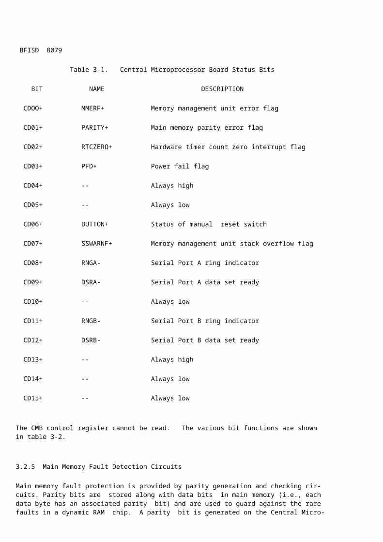
BFISD 8079
(Refer to the (MB Logic Diagram, sheet 34.) The W output of a 74LS151 l-of-8 data selector (7V) is the input to the segment-written bit of the 74S189 (7X). The W output always is high while the 68010 is in the supervisor mode. This is to allow the segment-written bit to be initialized before the 68010 switches to the user mode.
In the user mode, when a segment is written to, W is goes low and is stored in the 74S189. If the segment subsequently is read, then W will be the inverted value of the flip-flop (7S), which has been storing the segment-written bit of the 74S189. Thus the segment-written bit is preserved, even when a segment- read cycle occurs during the same segment access period. Timing signal CSTOF+ clocks the segment-written bit, in the status word register, into the flip-flop at the beginning of each memory access cycle.
A 74LS10 NAND gate (8S) and a 74LS08 AND gate (7W) create a write pulse for the status word register during user mode access or supervisor mode initialization. These gates AND signal CSTOF+ with PAENB- and the complement of CST1F+ to pro- duce a 125-nanosecond pulse. The pulse is gated through to the 74S189 status word register (7X) Write Enable input during a user mode memory access. During a supervisor mode write to the base address register, however, MMBWE- asserted provides the Write Enable input to the status word register.
Signal SEGWRT+ (SEGment WRiTe) is asserted when a memory write cycle occurs during the user mode. SEGWRT+ generates the Memory Management Write ERRor sig- nal (MMWERR+/MMWERR-) described in paragraph 3.2.16.8. This can occur only when the bit corresponding to output D03 of the 74S189 segment attribute reg- ister (3W) is set (refer to paragraph 3.2.16.6).
3.2.16.8 MMU Error Generation
The IvMERR- (Memory Management ERRor) signal is generated by any one of six MMUerror conditions, as listed in paragraph 3.2.16.3. A 74S30 NAND gate (10X) ORsthose conditions. (Refer to the CMB Logic Diagram, sheet 35.) MMERR- goes to the memory array stack via connector J03, pin C11. If the signal is assertedat the selected memory array board, then the PDTACK- (Processor Data TransferACKnowledge, required by the 68010 to complete a memory cycle) signal is block-ed from returning to the Central Microprocessor Board; the absence of PDTACK-creates a bus error exception signal, which is sent to the 68010, as describedin paragraph 3.2.10.
Signal MMERR+ is latched and held by a 74LS109 flip-flop (10R) at the end ofthe current cycle. The latched error becomes signal MMERF+ (Memory ManagementERror Flag) and is read in a (MB status read cycle, as described in paragraph 3.2.4. The error is reset at the end of the read, because the input of the flip-flop is low from CMBSTRE- ((MB STatus REad) asserted.
Signal SEGOVF- (SEGment OVer Flow) is generated by two MMU error conditions:
a. The memory access is a normal program fetch or data access (indicated by SEGDC1+ asserted) , and the address is equal to, or greater than, the limit address (indicated by ADLTLM+ inactive).
3-40

BFISD 8079
b. The memory access is a stack access (indicated by SEGDC2- or SEGDC3- asserted), and the address is less than the limit address (the stack address is out of bounds, indicated by ADLTLM+ asserted).
SEGOVF-, ORed with ABSEG-, produces the SAERR- (Segment Access ERRor) signal,which is written to the segment status word register, as described in paragraph3.2.16.7. (ABSEG- also is one of the ORed error conditions that generates theMMERR- signal.)
Signals MMWERR+ (Memory Management Write ERRor) and MMXERR+ (Memory ManagementeXecute ERRor) are inverted by two 74S00 NAND gates (8X) to produce signalsSWERR- (Segment Write ERRor) and SXERR- (Segment eXecute ERRor).
Signal SSWARN- (Stack Segment overflow WARNing) is the NAND (74LS08 [9S] and74LS04 [7R]) of SEGDC3+ and ADEQLM+ (logical ADdress EQual to LiMit address).SSWARN- indicates a stack segment is in the warning area (i.e., the last 512bytes before overflow). (SSWARN- is one of the ORed error conditions that gen-erates the MMERR- signal.)
SSWARN- also is latched and held by a 74LS109 J-K flip-flop (7S) (to becomeSSWARNF- [Stack Segment overflow WARNing Flag]) until the flip-flop is read bya CMB STatus REad (CMBSTRE-) signal. The flip-flop then is reset at the end ofthe status read cycle, when the K- input is low from the CMBSTRE- signal.
Signal RAMDIS- (RAM DISable) is provided to disable the MMU registers during"bed of nails" testing. (Refer to the CMB Logic Diagram, sheet 30.) When theinput of the 74LS04 inverter (4V) is pulled low by the tester, RAMDIS- goeshigh and disables the outputs of the 74S189 storage registers in the MMU.
3.2.17 Serial Ports
The following paragraphs cover detailed information on the serial interfacingof the Model 4108 Base Unit to peripheral devices. Controller circuitry thatwill support two serial I/O ports is contained on the Central MicroprocessorBoard, inside the Base Unit. Each port is an independent, 0- to IM-bit-per-second, full-duplex RS-232 channel. The ports can have different baud ratesfor transmitting and for receiving, and each port can support a printer, modemor terminal. Figure 3-10 shows a simplified block diagram of the serial portcircuitry, and the following circuit descriptions begin with a brief review ofsome basic serial interfacing principles.
3.2.17.1 Serial/Par all el Conversion
The serial port controller contains a bus interface through which the 68010 cansend commands to the ports, read port status, and access input and output dataregisters in the ports. An interrupt line notifies the 68010 of the completionof an operation. As in any serial port, a conversion takes place between theserial and the parallel data streams. Hence the interface with the 68010 is aparallel interface through which eight data bits are transmitted during a sin-gle transaction.
3-41

BFISD 8079

TBD

Figure 3-10. Simplified Block Diagram, CMB Serial Ports
3-42

BFISD 8079
The interface with a serial peripheral device, on the other hand, is a serialinterface in which those same data bits are transmitted on a single output lineor received on a single input line, one bit at a time. The conversion occursin the LSI serial communications controller chip, on the Central MicroprocessorBoard. The serial communications controller chip is a Zilog 8530 (2C). (Referto the CMB Logic Diagram, sheet 28.) The chip is a byte-wide device, residingon the byte-wide I/O data bus (described in paragraph 3.2.13). It is a multi-protocol and dual-channel device; and each independent channel, or port, canhandle 0- to IM-bits-per-second data transfer rates and full-duplex operation.A simplified block diagram of the 8530 chip is presented in figure 3-11.
Within the serial communications controller chip, an output register is loadedin parallel from the byte-wide data bus. This register, in turn, provides aparallel dump to a shift register. Hence data is loaded into the parallel reg-ister, then passed to the shift register, where the bits are collected untilthe register is full. Conversely, input data from a serial peripheral deviceare passed in parallel from an input shift register to an input data registerand then to the 68010, via the byte-wide data bus.
TBD
Figure 3-11. Simplified Block Diagram, 8530 SCC Chip
3-43

BFISD 8079
Serial Data Reception
The receive and transmit sections each have separate data registers because of a need to buffer data in transit through the port. There is a variable delay between the receipt of a byte-wide datum from a peripheral and the availability of a 68010 bus cycle that will accept that datum. Hence, the receive register accepts the datum and holds it during the time the input shift register is re- ceiving the next character. As each successive bit of the next arriving char- acter appears, the shift register shifts its present content to make room for the new datum.
This prevents the leading bits of the next character from overwriting the re- ceived datum. When the final bit of a character is received, the completed byte passes to the input buffer register, thus freeing the shift register to accept the next byte of serial information.
Serial Data Transmission
A similar, but reverse, series of events occurs during the transmit cycle. The benefit in this case stems from the elimination of idle time between character bytes on the serial output line. The moment the final bit of a character byte leaves the output port, a new data byte is moved into the output shift register from the output buffer register. Now the 68010 has the entire 8-bit character interval to reload the output buffer register. This ability to eliminate idle time between characters is of fundamental importance in synchronous communica- tions protocols.
3.2.17.2 Communications Protocol Selection
A communications protocol is a convention for data transmission that includesat least the following functions.
o Timing
o Formatting
o Control
o Representation of data
The Model 4108 Base Unit provides flexibility in configuring the transmit andreceive parameters of the serial ports for various protocols. The ports cansupport three catagories of serial protocols. Each port can be configured as
o synchronous,
o standard asynchronous, or
o asynchronous, with programmable split baud rate (i.e., transmit and receive can be at different rates, from 150 baud to 19.2K baud).
3-44

BFISD 8079
Synchronous Protocol
In the synchronous mode, each successive datum in a data stream is controlledby a master data clock. Hence the clock controls not only the bits within acharacter byte, but the character-to-character spacing as well. (One benefitof this method is higher communication speed, as an entire block of data may beexchanged, with only normal bit spacing between characters.) The master clockis received as an additional signal, separate from the incoming data stream.This clock appears at the Port A DB-25 connector (J09, pin 17) as signal RTXCA+(Receive/Transmit Clock, Port A).
From there it is routed, via a 74LS153 l-of-4 data selector (2J), to the RTXCA-input of the serial communications controller chip, or SCC. (Refer to the CMBLogic Diagram, sheets 28 and 29.) A similar path is found from the Port B DB-25 connector (J10, pin 17) to the SCC.
Standard Asynchronous Protocol
The standard asynchronous mode selects the 3.6864 MHz clock from a local oscil-lator (2K) and feeds that to the SCC via the same data selectors (2H and 2J).In asynchronous serial data transmission, each character is treated as an indi-vidual message; each appears in the data stream at an arbitrary time. Thus itis the responsibility of each character to inform the receiving serial port ofthe beginning and the end of that character. It does this with start bits andstop bits. When no data is being transmitted, the data line carries a logic 1level (high voltage).
When a datum appears on the line, the first bit received is a logic 0 (low);this commands the SCC to begin sampling the datum. The next 8 bits are databits, and the final 1, 1-1/2, or 2 bits are stop bits. The stop bits are al-ways at logic 1 (high).
Split Baud Rate Asynchronous Protocol
The split baud mode allows serial transmission at one data rate and receptionat another. The mode is selected by system software using data bits CD02+ andCD03+ (or CDOO+ and CD01+ for Port B). These data bits are latched in a 74S373transparent latch (3K). Refer to the CMB Logic Diagram, sheet 29.) The localbaud rate clock for transmitting data is selected by data bits CD05+, CD06+ andCD07+, latched in the same 74S373. The SCC is programmed directly to set thebaud rate of the receive clock.
A 74LS163 binary counter (3G) divides by 8 the output of a 4.915 MHz oscillator(4G). A 74LS393 binary counter (3H) generates 8 clock rates, each equal to 16times the frequency of the requested baud rate. These are the clocks that areselected by data bits CD05+ through CD07+.
Data bits CD05+ through CD07+ are decoded in a 74LS151 l-of-8 data selector(3J). The other data bits select which of the three possible clock sources isto be used for each port on the SCG.
3-45

BFISD 8079
They are selected by the 74LS153 data selectors that were mentioned earlier (2J and 2H). The control and data bits are available to the SCC when the SCC is selected by the local I/O address decoder (discussed in paragraph 3.2.12.4) in the Central Microprocessor Board.
3.2.17.3 Electrical Configuration Selection
To further define the asynchronous serial communications protocol used in the Model 4108 Base Unit, we separate the logical conventions from the electrical connection requirements. The electrical connections used in asynchronous pro- tocols usually are referred to as one of the following:
o RS-232-C
o 20 mA current loop
o RS-422, RS-423, or RS-449
Of these, the Base Unit uses only RS-232-C and RS-422.
RS-232-C
The RS-232-C standard originally was intended to provide a specification for using modems (modulator/demodulator) to connect remote devices to computers, via the telephone network. The standard now is used to connect the computers directly to terminals and to serial printers, in addition to modems.
The RS-232-C standard defines 21 signals and a 25-pin electrical connector for asynchronous serial data communication. In order to accommodate terminals and serial printers in addition to modems the serial port circuitry in the Central Microprocessor Board must be electrically configured for the desired peripheral device. Hence that circuitry contains several connections for jumpers to allow the necessary reconfiguration. Table 3-6 shows the signal names, their corre- sponding cable pin number, jumper reference letters, and the circuit board pin numbers of the pins that must be connected together by the jumper wires for a particular configuration.
Note that only kind of one cable is needed to support printers, terminals or modems. All signal switching is done on the Central Microprocessor Board via the jumpers. The RS-232 cable is a pin-for-pin connection; no signals or pins are cross-connected.
RS-422
The RS-422 standard describes the electrical characteristics of a port that is designed to allow a higher signaling rate bandwidth over longer distances than is provided by the RS-232-C. This standard defines a double-ended electrical interface that can signal at data rates well in excess of the 20-kHz bandwidth allowed by RS-232-C (20 kHz = 20K data bits/second) .
3-46

BFISD 8079
Table 3-6. Serial Port Electrical Configuration Jumper Connections
PORT A:
MODEM TERMINAL PRINTER
Name Jumper A Cable Jumper A Cable Jumper A Cable
CTS 7 and 8 pin 5 7 and 9 pin 4 7 and 9 pin 4DSR 3 and 4 pin 6 *1 and 3 pin 20 1 and 3 pin 20DTR 1 and 2 pin 20 *2 and 4 pin 6 2 and 4 pin 6RTS 9 and 10 pin 4 8 and 10 pin 5 8 and 10 pin 5RXD 11 and 12 pin 3 11 and 13 pin 2 11 and 13 pin 2TXD 13 and 14 pin 2 12 and 14 pin 3 12 and 14 pin 3RNG In Place pin 22TRXC In Place pin 15DCD In Place pin 8
PORT B:
MODEM TERMINAL PRINTER
Name Jumper B Cable Jumper B Cable Jumper B Cable
CTS 7 and 8 pin 5 7 and 9 pin 4 7 and 9 pin 4DSR 3 and 4 pin 6 3 and 1 pin 20 3 and 1 pin 20DTR 1 and 2 pin 20 2 and 4 pin 6 2 and 4 pin 6RTS 9 and 10 pin 4 8 and 10 pin 5 8 and 10 pin 5RXD 13 and 14 pin 3 13 and 15 pin 2 13 and 15 pin 2TXD 15 and 16 pin 2 14 and 16 pin 3 14 and 16 pin 3
Jumper G Jumper G Jumper G
RXD 15 and 16 pin 3 15 and 16 pin 2 15 and 16 pin 2DCD 17 and 18 pin 8 17 and 18 pin 8TRXC 10 and 20 pin 15 19 and 20 pin 15 23 and 24 23 and 24
Jumper H Jumper H
DCD 1 and 2 1 and 2
Jumper K Jumper K Jumper K
D422 *1 and 2 *1 and 2 *1 and 2
NOTE: Be sure to disconnect all unused jumper positions on port B.
*This jumper disables the RS-422 drivers.
3-47

BFISD 8079
In the Model 4108 Base Unit, only Port B can be configured for RS-422; although either port may be used as a synchronous data channel , it may be advantageous to use port B, because of the balanced link associated with the RS-422 config- uration. In the serial port input/output circuitry, the RS-422 line drivers are 26LS31s (4D), and the receivers are 26LS32s (4C). (Refer to the CMB Logic Diagram, sheet 28.1.)
3.2.17.4 Addressing and Control
The 8530 SCC chip (20) is enabled with a 68010 supervisor read or write to ad- dress 60XXXY (hex). The internal registers of the SCC chip are addressed by address bits A014A and A02-fA, from the 68010. Port A is selected when A02+A is high; Port B is selected when that bit is low. Address bit A01+A. informs the the SCC that either data or control parameters are being sent.
The read and write strobes to the SCC are synchronized by ANDing their comple- ments with the CST4F+ timing signal to meet SCC timing requirements. This is done by a 74LS51 combination gate (9M) . (Refer to the CMB Logic Diagram, sheet 25.) A reset on RSTF2+ will cause both a read and a write to be sent to the SCC, creating the required reset condition. Table 3-7 shows the data bus bit patterns required for selecting the various serial port logical configurations and data rates.
Once a port has been selected and configured, and data transfer is in progress, the system software needs to be informed of when a datum has been transferred between a shift register and a buffer register in the SCC chip. This is so that a driver routine can either load a new byte into the transmit buffer or transfer the new byte in the receive buffer to the 68010.
When a byte of data has been tranferred between a buffer register and a shiftregister, control logic in the SCC chip activates the interrupt pin (INT-) ofthe chip. (Refer to the CMB Logic Diagram, sheet 28.) When this pin is low,signal INT5- (INTerrupt level 5) is encoded by a 74LS148 8-line-to-3-line pri- ority encoder (3E). (Refer to the CMB Logic Diagram, sheet 22.) This consti- tutes an interrupt request to the 68010.
Thus an interrupt request level 5 is encoded on the 68010 interrupt requestlines (IPLO- through IPL2-). If the priority of the interrupt is greater than the current processor priority, then the interrupt processing sequence begins.The 68010 places the interrupt priority number on the lines carrying the threeleast significant address bits. These are decoded by a 74LS151 1-of-8 data se-lector (10K, CMB Logic Diagram, sheet 22).
For priority number 5, the CVPA- (CPU Valid Peripheral Address) output of thedata selector is low (active). In response to CVPA-, the 68010 internally gen-erates a vector number that is determined by the interrupt level number. (Thevector number [when multiplied by four] is the address in the lowest 1K bytesof main memory that contains the beginning address of the routine that willhandle the interrupt.) The content of the vector number is fetched and loadedinto the 68010 program counter, and normal instruction execution commences inthe interrupt service routine.
3-48

BFISD 8079
Table 3-7. Bit Patterns for Serial Port Configuration and Data Rate Selection
DATA BUS
CD03+ CD02+ CD01+ CDOO+ LOGICAL PORT CONFIGURATION
0 0 X X Port A, Synchronous
0 1 X X Port A, Asynchronous
1 0 X X Port A, Split Baud Rate
X X 0 0 Port B, Synchronous
X X 0 1 Port B, Asynchronous
X X 1 0 Port B, Split Baud Rate
CD07+ CD06+ CD05+ CD04+ TRANSMIT BAUD RATE
0 0 0 X 19,200
0 0 1 X 9,600
0 1 0 X 4,800 . 0 1 1 X 2,400
1 0 0 X 1,200
1 0 1 X 600
1 1 0 X 300
1 1 1 X 150
Note: 1 = High; 0 = Low; X = Don't care
The program now can read the status register in the SCC to determine whetherthe interrupt was due to the transmission or reception of data; then the 68010can move data to or from the SCC chip.
At the same time that the priority number on the address bus was being decodedto produce CVPA-, a 74LS138 1-of-8 decoder (10L, CMB Logic Diagram, sheet 20)also decoded those address bits. The output is the IACKL5- signal. This in-terrupt acknowledge signal is synchronized to the system clock in a 74LS74 Dflip-flop (10J). (Refer to the CMB Logic Diagram, sheet 25). The output ofthe flip-flop is the SCC INT- input to the SCC chip, which resets the interruptlogic in the chip.
3-49
BFISD 8079
3.2.18 Parallel Port
In the following paragraphs we discuss the interfacing of external devices to the Model 4108 Base Unit through the parallel I/O port. Controller circuitry to support the parallel port is contained on the Central Microprocessor Board, inside the Base Unit. Although the port is a general-purpose I/O channel that can be used for a variety of 8-bit parallel interfaces, it usually will be used to interface a printer with the CentronicsTM "standard" interface. The follow- ing detailed discussion assumes that such a printer is connected to the port.
The parallel port uses a Motorola 68230 Parallel Interface/Timer, or PI/I. The PI/T (5D) is a byte-wide device and resides on the byte-wide I/O data bus (de- scribed in paragraph 3.2.13). (Refer to the CMB Logic Diagram, sheet 26.) The PI/T has two 8-bit ports and also has a timer with a separate interrupt output. The PI/T is permanently configured with Port A as the output port and Port B as the input port.
3.2.18.1 Addressing and Control
The 68230 PI/T chip (5D) is enabled with a 68010 supervisor read or write to address 62XYYX (hex). This provides the PI/T Chip Select (CS-) input with an enable strobe that is the AND of signals PITCE- and CST1F+ (from a 74LS00 NAND gate [4E]. Signal PITCE- (PI/T Chip Enable) comes from the local I/O decoder described in paragraph 3.2.12.4. Signal CST1F+ is a timing signal that comes from the timing generator described in paragraph 3.2.10.1. The two signals are ANDed so that the PI/T can start the strobes on a clean clock edge (CST1F+).
The internal registers of the PI/T chip are addressed by address bits A044A through A084A, from the 68010. The read and write strobe to the PI/T is the CRNW- (CPU Read Not Write) strobe from the 68010. The pin labeled DTACK pro- vides a Processor Data Transfer ACKnowledge (PDTACK-) signal , required by the 68010 during a bus cycle to indicate the number of wait states, if any, to in- sert in the cycle (this is discussed in paragraph 3.2.10). Pins HI and H2 are for input and output "handshake" strobes.
Pin H4 is tied to pin B7, which receives the high-order bit (PB07+) of the in- put parallel port; this is a BUSY bit from the printer, which is used to gener- ate an interrupt. The parallel control ports are wired for interrupt level 1 (INT1-), and the timer for interrupt level 6 (INT6-).
(Although the parallel port has the lowest interrupt priority [level 1], the timer in the PI/T chip has the highest priority, next to the power fail detect interrupt. This is because the interrupt generated by that timer is used to provide the "time slices" required for multi-user operation.)
When the printer is ready toreceive a byte of data, the BUSY bit (PB07+), from the printer, goes goes high. Since this bit also enters pin H4 of the PI/T, the chip asserts the interrupt signal from the pin labeled PIRQ-. This signal signal (INT1-) is encoded by a 74LS148 8-line-to-3-line priority encoder (3E). (Refer to the CMB Logic Diagram, sheet 22.) The output of the encoder consti- tutes an interrupt request to the 68010.
3-50

BFISD 8079
Thus an interrupt request level 1 is encoded on the 68010 interrupt requestlines (IPLO- through IPL2-). If the priority of the interrupt is greater thanthe current processor priority, then the interrupt processing sequence begins.The 68010 places the interrupt priority number on the lines carrying the threeleast significant address bits. These are decoded by a 74LS151 l-of-8 data se-lector (10K, CMB Logic Diagram, sheet 22).
For priority number 1, the CVPA- (CPU Valid Peripheral Address) output of thedata selector is low (active). In response to CVPA-, the 68010 internally gen-erates a vector number that is determined by the interrupt level number. (Thevector number [when multiplied by four] is the address in the lowest IK bytesof main memory that contains the beginning address of the routine that willhandle the interrupt.)
The content of the vector number is fetched and loaded into the 68010 programcounter, and normal instruction execution commences in the interrupt serviceroutine. The program now can write a data byte to the data register in thePI/T, for transmission to the printer.
3.2.18.2 Data Transmission to a Printer
The output data format from the parallel port is ASCII (American Standard Codefor Information Interchange); it's the same format used in the serial ports.The parallel data output is asynchronous, and the data transfer rate is deter-mined by the transfer program, which normally is interrupt driven. The driversand receivers in the parallel port circuitry are 74LS244s (4B and 5A). (Referto the CMB Logic Diagram, sheet 27.) These are connected to J13, the parallelport connector, which has 37 pins. Table 3-8 is a list of the J13 signals. Aprinter connected to the Model 4108 Base Unit parallel port typically will usethe so-called "Centronics parallel interface standard." Table 3-9 gives a de-scription of the Centronics protocol.
3.2.19 Floppy Disk Controller
Two floppy disk(ette) drives may be mounted inside the Model 4108 Base Unit ofthe MAI® 2000 SeriesDesktop Computer System. The driven diskettes are 5.25inches in diameter, contain 96 tracks per inch (TPI) of diskette radius and aredouble-sided. Controller circuitry to support both floppy drives is providedon the Central Microprocessor Board. The circuitry provides for soft-sectoredand double-density recording techniques. Figure 3-12 shows a simplified blockdiagram of the controller, and the following paragraphs describe the circuitry,beginning with a very brisk review of a few basic disk recording principles.
3.2.19.1 Soft Sectoring
Soft-sectoring means there are no sector holes in the diskette to identify thehead position with respect to a track. Instead, a single hole provides a phys-ical reference point, and sector information is recorded magnetically on thedisk within each sector.
3-51

BFISD 8079
Each sector contains an identifier field that appears on the data stream justbefore the data field. To read data, the head is first positioned at the cor-rect track, where it reads the data stream continuously. When the read/writehead detects an identifier with thecorrect sector number, the data block fol-lowing that identifier is accepted.To write a new data block, the disk controller first reads data continuouslyuntil an identifier is located with a matching sector number. The controllerthen rewrites the new data over the existing data block in that sector. Theidentifiers, however, are never rewritten during normal operation, though thecontroller has the capability of writing those identifiers onto a blank disk-ette when that diskette is being initialized for first use. The soft-sectoringtechnique is so called because the system software can revise the sector formatof a diskette by rewriting the sector identifiers.
Table 3-8. Parallel Port (J13) Connector Signals
PIN PI/T SIGNAL DRIVER/RECEIVER SIGNAL FUNCTION
1 PAOO+ PDTOO+ 2 PA01+ PDT01+ 3 PA02+ PDT02+ 4 PA03+ PDT03+ 5 PA04+ PDT04+ 6 PA05+ PDT05+ 7 PA06+ PDT06+ 8 PA07+ PDT07+ 9 PBOO+ PDTIO+ 10 PB01+ PDTI1+ 11 PB02+ PDT12+ 12 PB03+ PDTI3+ PAPER EMPTY 13 PB04+ PDTI4+ SAFETY SWITCH 14 PB05+ PDTI5+ SELECT 15 PB06+ PDTI6+ 16 PB07+ PDTI7+ BUSY 17-27 GND 28 DTISTB1+ 29 GND 30 DTOSTB1- 31-35 GND 36 +5V 37 N/C
3-52

BFISD 8079
Table 3-9. Centronics Protocol
SIGNAL DESCRIPTION CONNECTOR (J13) PIN
Data Strobe Sent by the Model 4108 Base'Unit 30 to cause the printer to accept information on the data lines. The data lines must stabilize at least 50 nanoseconds before the Data Strobe is sent. The Data Strobe must be present for at least 100 nanoseconds and must be removed at least 50 nanoseconds before the data is taken from the data lines
Busy Sent by the printer to indicate that 16 the printer cannot accept data
ACKNLG- Sent by the printer to indicate that 28 a character or a function code has been accepted
Data Bit 1 Sent by the Model 4108 Base Unit 1
Data Bit 2 Sent by the Model 4108 Base Unit 2
Data Bit 3 Sent by the Model 4108 Base Unit 3
Data Bit 4 Sent by the Model 4108 Base Unit 4
Data Bit 5 Sent by the Model 4108 Base Unit 5
Data Bit 6 Sent by the Model 4108 Base Unit 6
Data Bit 7 Sent by the Model 4108 Base Unit 7
Data Bit 8 Sent by the Model 4108 Base Unit to 8 control the optional character set
SS Always at 0 volts ??13??
PE Sent from the printer to indicate an ??12?? out-of-paper condition or that the printer cover is open. A positive level is logical true
SLCT Sent from the printer when the +5V ??14?? supply is on, the paper is loaded, the front cover is closed, and the operator has activated ON LINE
3-53

BFISD 8079

TBD

Figure 3-12. Simplified Block Diagram, CMB Floppy Disk Controller
3-54

BFISD 8079
A hard-sectored format, on the other hand, allows somewhat greater data densitythan does a soft-sectored. This is because no identifier field occupies spacethat otherwise is usable for data. However, the advantages of a soft-sectoredformat are many, and the double-density disk recording techniques, described inparagraph 3.2.19.2, more than compensate for the data density problem.
3.2.19.2 Double-Density Recording
The double-density recording scheme also is known as MFM (modified-frequencymodulation) encoding. This encoding scheme may best be understood by firstreviewing the Kansas City Standard (KSC) for cassette recording. The KSC en-coding technique is shown in figure 3-13. A binary 0 is recorded as four fullcycles of a 1200—Hz square wave. A binary 1 is recorded as eight full cyclesof a 2400-Hz square wave. Clearly, with this encoding scheme the transmissionrate for one data bit is 1/8 of 2400 Hz, or 300 data bits/second.
The transitions that are common to both the binary 0 and the binary 1 are usedto synchronize a local oscillator to the incoming data rate, when the data arerecovered from the recording. Therefore, when a transition occurs between theclock ticks, the data recovery circuitry may assume that a 1 is encoded; other-wise the circuitry may assume the code is a binary 0.
TBD
Figure 3-13. Signal Encoding and Derived Clock, Kansas City Standard
3-55

BFISD 8079
The transmission rate of the Kansas City Standard can be increased by simplyusing fewer transitions to encode each datum. Figure 3-14(a) shows a binary1100 sequence encoded at a transmission rate of 1200 bits/second. Here the bi-nary 0 requires one full cycle of 1200 Hz, and the binary 1 requires two cyclesof 2400 Hz. Figure 3-14(b) shows the standard pushed to the maximum data rateof 2400 bits/second. In this scheme a binary 0 is recorded as half a cycle of1200 Hz, and a 1 is recorded as a full cycle of 2400 Hz.
Regardless of the data rate, the information in Kansas City Standard recordingsis in the transitions of the recorded data. At a maximum data transfer rate,the derived clock rate is identically equal to the frequency of the logic 1cycle. Therefore, the logic 1 cycle has a transition in the middle of a clockcycle. On the other hand, the logic 0 cycle has no such transition. A maximumdata transfer rate is used in FM encoding. The FM encoding technique recordson the disk only the transitions of the data square waves, as shown in figure3-15. This means that the clock frequency can be increased to pack the databits more closely on the disk track than can be done when the entire squarewave is recorded, as with cassette recording.
This is not the final limit, however. There is a way of recovering the clock-ing information without wasting half the bits, thereby doubling the number ofinformation bits on a disk. The method is called both double-density and MFMencoding. With this scheme, the encoder discards the clock bits so that onlythe data bits are present in the output bit stream.
TBD
Figure 3-14. Maximum Data Rate Recording, Kansas City Standard
3-56

BFISD 8079
TBD
Figure 3-15. Encoded Data for FM Recording
Clearly, both the data transfer rate and the amount of data on the diskette nowcan be doubled with respect to the (single-density) FM method. To recover thedata, the detector section of the disk controller circuitry generates a pulsestream equal in frequency to the data rate. These narrow pulses create a bitwindow in which a logic 1 is detected as a flux transition in the middle ofthat window, and a logic 0 is detected as an absence of a transition. So thecontroller can be sure of the location of each 0 in a long string of Os, theencoder section records (on the diskette) the clocking information by insertinga clock transition between two adjacent Os, as shown in figure 3-16.
Hence, the MFM detector is more complex than the FM detector, because it mustrespond to the inserted clock bits, which appear coincident with the bit windowpulses. The FM and MFM detectors usually are called data separators, becausethe detector works with a phase-locked loop to separate the composite clock anddata signal into clock-only and data-only signals.
3.2.19.3 MFM Data Separation
Data separation in the case of MFM is somewhat different from that of FM. InFM data separation, the data and the clock components of the composite signalare truly separated: only data pulses go to the controller data input. On theother hand, in MFM data recovery, the data input to the controller comprisesall the original bits from the disk, both data and clock.
The clock input to the floppy disk controller is not the clock pulses containedin the composite signal but is a synthesized version, generated by a local os-cillator in a phase-locked loop. The clock pulses from that phase-locked loopcreate a window during which a data bit is expected. The data input from thediskette to the controller is gated from that window. Separation of the databits from the clock bits takes place inside the floppy disk controller chip(paragraph 3.2.19.5), where the actual window gating occurs. (In FM detectionthe gating usually takes place in the data separator.)
3-57
BFISD 8079
TBD
Figure 3-16. Encoded Data for Modified FM (MFM) Recording
Phase Detection
Data separation is enabled by the VCOE+ (VCO Enable) signal input to a 74LS51combination gate (13X). (Refer to the CMS Logic Diagram, sheet 51.) The VCOE+signal comes from the floppy disk controller chip and is asserted (high) whenthe chip is ready to transfer data to or from the diskette. The pin 6 outputof the combination gate directs the data from the diskette (DSKDAT-A [DiSKetteDATa]) to a 74LS221 one-shot (14Z). The one-shot delays the data pulse so thata phase detector can detect any clock pulse (generated by a local oscillator)occuring prior to the delayed data pulse, for synchronization purposes. (Afterthe delay, the data pulse is regenerated by another 74LS221 one-shot after an-other short delay through the other section of the combination gate [pin 8]).
At the moment the one-shot is toggled by a data pulse, the Q output (pin 5)enables the phase detector logic of the phase-locked loop, by clocking a 74LS74D flip-flip (14X, pin 3) to a cleared condition. Before or after the one-shotclears, a clock pulse from the local oscillator will trigger another 74LS74 Dflip-flop (14X, pin 11)--this is guaranteed because this clock pulse representstwice the data transfer rate. When the one-shot clears, the Q- output clocksyet another 74LS74 D flip-flop (14V), which indicates the leading edge of thedelayed data pulse.
The Q- outputs from the last two flip-flops mentioned are ANDed in a 74LS02 NORgate (14W). Any time these outputs are coincident (both low), the NOR gateoutput sets the flip-flop (14X, pin 4) that enabled the phase detector logic.This flip-flop, in turn, clears the other two flip-flops (14V and 14X), effec-tively turning off the phase detector.
Thus the phase detector is enabled and disabled once for every pulse on thedata line from the diskette. This allows synchronization of the clock to thedata even though the data input to the phase-locked loop is not a square wavewith a 50% duty cycle, but rather a stream of narrow pulses, with many pulsesmissing from their nominal location.
3-58

BFISD 8079
A simplified and generalized block diagram of the phase detector logic is shownin figure 3-17. To help the reader to understand the phase detector logic, theblock diagram contains only generic logic blocks, and all signals are positivelogic (active high), regardless of their true active voltage level. Statechanges occur only on rising edges.
Clearly, there was some delay between the time one flip-flop was triggered bythe data pulse and the time the other flip-flop was triggered by the clock.The delay is indicated by a low output from the NOR gate (14W, pin 10), whichallows the phase detector to continue working. The delay also is representedby positive-going pulses from one of the phase detector flip-flops and by neg-ative-going pulses from the other.
These PUMP UP (negative-going) and PUMP DOWN (positive-going) signals, whenfiltered, drive a voltage-controlled oscillator, or VCO. PUMP UP tends to in-crease the average frequency of the VCO, and PUMP DOWN does the opposite. Thisaction indicates the outcome of the race between a pulse in the incoming datastream and a VCO clock pulse.
TBD
Figure 3-17. Simplified Block Diagram, Data Separator Phase Detector Logic
3-59

BFISD 8079
For example, if the VCO clock pulse (via a 74LS161 synchronous 4-bit counter [15T]) toggles the flip-flop (14X) connected to it before the pulse from the diskette toggles the other flip-flop, then PUMP DOWN will produce a pulse. The pulse informs the VCO that it is generating too high a frequency, and the pulse will bring down the voltage reference going to the MC4024 VCO chip. The pulse will be active for the time between the leading edge of the VCO clock pulse and the leading edge of the delayed data pulse, indicated by the Q- output of the one-shot (14Z, pin 12) going low.
The opposite happens when a delayed data pulse appears before the clock ticks. In this case, PUMP UP is a negative pulse, whose width is proportional to the error between the two pulses. The clock used for comparison is taken from the third bit of a synchronous 4-bit counter (15T) to provide a clock frequency of two times the actual bit transfer rate. This is so the VCO will synchronize with both the data bits and the inserted clock bits in the input data stream (the inserted clock bits occur at twice the data bit rate).
(To maintain a nominal VCO frequency when no data is being transferred to or from the diskette, the VCO is synchronized with a signal (2XWRCLK+ [2X WRite CLocK]) that is twice the frequency of the clock used to send data to the disk- ette. When the VCOE+ signal goes low, the pin 6 output of the 74LS51 combina- tion gate (13X) replaces the data with the 2XWRCLK+ signal, and synchronization occurs as before.)
Analog Error Detection
The pulse width of the PUMP UP and PUMP DOWN error signals is proportional to the required amount of frequency correction. Each of these pulse trains looks like a pulse-width-modulated replica of the input data stream. The difference in the average voltages of the pulse trains determines the output frequency of the VCO, which is an MC4024 (15V). Only one of these error signals is active at any given time; neither is active when synchronization is exact. However, when synchronization is exact, both flop-flops will be set when the data pulse and the clock pulse arrive at the CLOCK inputs to the flip-flops. This means that both flop-flops will be set for a short period of time, until the low out- put from a NOR gate (14W) turns off the phase detector logic and resets them.
During this time, the high pulse on the PUMP DOWN line is supplied through a diode (CR4) and series resistance to a capacitor (C125). The capacitor charges to a positive level. The charge creates an "automatic bias" for the base of one of the transistors (Q2) used to adjust the VCO control voltage. This nomi-nal bias level sets the reference voltage for the VCO. The bias increases (be- comes more positive) when a positive pulse comes in on the PUMP DOWN line; but,when a negative pulse (actually a low positive pulse) arrives on the PUMP UP line, the bias charge will "leak" out through the other diode (CR3), to ground,and thereby decrease the bias to the error amplifier input transistor.
The error amplifier is a dc amplifier consisting of two 2N2222 transistors con-nected in a superalpha configuration, for proper impedance matching and good stability. An RC (R33/C124) negative feedback loop helps filter the high fre- quencies in the pulse transitions.
3-60

BFISD 8079
Thus the error amplifier and phase detector logic circuits provide necessarycorrections to the VCO frequency to ensure synchronous clocking of data bitsfrom the diskette into the floppy disk controller chip. However, certain ac-tivity occurs during the writing of data onto the diskette that degrades theread data and that cannot adequately be compensated for by the data separator.The phenomenon is known as "bit-shifting."
3.2.19.4 Bit-Shifting
A problem peculiar to magnetic disk recording, especially MFM recording, isthat the high bit densities cause the recovered data to appear shifted fromtheir nominal position. Figure 3-18 shows the phenomenon as it appears to thefloppy disk controller chip. The upper trace shows five data pulses recordedon the diskette at the apparent positions indicated. When the pulses are readback from the diskette, they are shifted in time from their apparent recordedposition (i.e., some pulses appear later; o.thers appear earlier), as shown inthe lower trace.
Several factors, which include nonlinearities in the pickup electronics andmagnetic interactions, are responsible for bit-shifting. For example, the datapulses correspond with magnetic domains on the diskette. As shown in the uppertrace of figure 3-18, the leftmost bit has a bit on its right but not on itsleft. Therefore, its magnetic domain is influenced by a like magnetic pole onthe right, but not on the left. The magnetic flux of the leftmost bit thus isdistorted and tends to move away from the nearby right-hand pole. Also, thesituation may be aggravated by a real movement of the domain to the left.
TBD
Figure 3-18. Bit Shifting
3-61

BFISD 8079
Consequently, the read head, responding to the magnetic flux lines of the re- corded data bit, sends the bit to the drive electronics as if it were repelled by the bit that will arrive after it (which is the bit to its right in figure 3-18). This means that the bit seems to arrive early.
The data separator circuits (discussed in paragraph 3.2.19.3) cannot adequately compensate for bit-shifting; this is because the phase-locked loop in the data separator is a feedback-control system that cannot follow sudden changes in in- put frequency, but rather settles over a period of time to its steady-state be- havior .
Therefore, another means of bit-shift compensation is provided. The method used does not actually compensate for the bit shifting of recorded data; but rather it compensates for the anticipated bit shift, before data actually is recorded. The method is called "precompensation."
Precompensation
Fortunately, the data bit flux transitions appear early or late in a completely predictable manner. Their time of arrival (at the read electronics) depends on the location of other bit transitions in their immediate vicinity. Since the floppy disk controller chip holds a byte of data before that data goes to the diskette, the controller is in a position to analyze the locations of the data bits within that byte and, in turn, to determine which bits will suffer from bit-shifting.
For example, if a data bit is a 0 and has a 1 bit on each side of it, then the neighboring bits will be shifted toward the missing data pulse when they are recorded on the diskette. Hence, the first bit should be written early and the second bit should be written late, to compensate for the shifting. The appro- priate commands for this are provided by the floppy disk controller chip and delivered to the precompensation logic.
Precompensation Control
The amount of precompensation is determined by a 74LS195 4-bit parallel-access shift register (13S). (Refer to the CMB Logic Diagram, sheet 49.) Each time a data pulse (WD4- [Write Data]) arrives from the floppy disk controller chip, the pulse is synchronized with FDCCLK+ (Floppy Disk Controller CLocK) and clock signal K4MHZ- (origin of both is in the clock generator section of the Central Microprocessor Board). This gives the broadside input logic, of the shift reg- ister enough time to set up before it latches the timing control commands from the floppy disk controller chip and begins shifting.
If the shift register receives an EARLY+ command from the controller chip, then that command becomes the data bit and is shifted out of the shift register 125 nanoseconds earlier than the nominal write time. This will compensate for the shift that occurs when that bit is written to the diskette. (The EARLY+ com- mand is gated through a 74LSOO NAND gate [13R] to input C of the shift regis- ter.)
3-62

BFISD 8079
Likewise, if the shift register gets a LATE+ command from the controller chip,then that command becomes the data bit and is shifted out of the shift register125 nanoseconds later than the nominal write time. (The LATE+ command is gatedthrough the 74LSOO NAND gate [13R] to input A of the shift register.)
However, if both commands are inactive (low), then they are ANDed by the 74LS00NAND gate (13R) and sent to input B of the shift register. In this case, thatANDed signal becomes the data bit and is shifted out at the nominal write time.The data bit output of the shift register is taken from the QD- pin and is sentto the drive electronics via a 7406 open-collector inverter (14J, pin 8).
Although the preceding discussions have assumed the reader is acquainted withthe WD1793 floppy disk controller chip, such an acquaintance is not absolutelymandatory to understand the material up to this point. However, as we continuewith functional descriptions of the remaining circuits in the floppy controllersection, it becomes more important to understand the basic architecture of thechip. An overview of the chip is presented in the following paragraph.
3.2.19.5 Floppy Disk Drive Control
The floppy disk controller section of the Central Microprocessor Board is basedon the WD1793 floppy disk controller chip (14R). (Refer to the CMB Logic Dia-gram, sheet 50.) The chip has the capability to read and write in single ordouble density. But it is used only in the double-density mode in our system.
The chip controls head motion by issuing step pulses and head-load commands tothe drive. Step pulses move the read/write head arms from from track to track.The head-load command makes the head contact the diskette surface. (When thehead is not loaded, it is physically lifted from the diskette surface.) Thechip also combines the clock and the data bits to form a composite serial datastream, to be recorded on the diskette. And it also assembles the separateddata and clock bits into 8-bit bytes for transmission the 68010.
Note that only a few external chips are required to interface the controller tothe floppy diskette drive, since almost all aspects of diskette control are em-bedded in the controller chip. It operates on its own 2 MHz clock and has anon-chip processor designed for disk drive control. The chip occupies four mem-ory addresses: the internal command/status, track, sector and data registerseach have unique addresses, and can be read from and written to. (The registerlayout is shown in figure 3-19.)
The track register contains the track number of the arm position of the disk-ette drive that is presently selected. When a new drive is selected, the trackregister momentarily is incorrect. But when a system software command is givento the controller chip to read the diskette, the track identifier, as it passesunder the head, is loaded into that register.
The sector register indicates which sector is to be read from or written to.When the controller executes a read or a write instruction, it first puts thehead in contact with the diskette (it "loads the head"). Then it reads thesector IDs at the present arm position.
3-63

BFISD 8079
TBD
Figure 3-19. Register Layout, WD1793 Floppy Disk Controller Chip
The controller checks each ID for a match against the contents of the track andsector registers. As the disk rotates, the correct sector arrives under thehead. This is indicated by a match of the ID to the track and the sector reg-isters. Now the controller is ready to read or write the data immediately fol-lowing the sector ID. The data read from the diskette are accumulated bit bybit in the controller until a full byte is present. The byte is in the dataregister (in the chip) and will be passed to the 68010 over the byte-wide databus.
Data to be written to the diskette flow from the 68010 to the controller chipover the same byte-wide data bus. These data are stored in the data register(in the chip) by parallel 8-bit write cycles. They then are output as a serialbit stream to the diskette drives.
The remaining two registers are the command register and the status register.These occupy a single address in the floppy controller I/O address space. Dataread from this address are status reports to be returned to the 68010; datawritten to this address are commands interpreted by the controller chip.
3-64

BFISD 8079
There are 11 commands available on the WD1793; they are listed in table 3-10.The Type I commands move the arm to the correct track. STEP IN and STEP OUTcommands move the arm one track in or out. The STEP command moves the arm onetrack in the same direction as the last arm movement. The SEEK command allowsthe arm to be moved several tracks in a single step. This command accepts atarget track number, contained in the data register, and then issues the cor-rect number of step pulses to move the head arm from the present track to thetarget track.
The Type I commands generate the appropriate signals at the controller chippins labeled STEP+ and DIRECTION*. In addition to these arm control signals,there are four output signals for writing data:
o WD+ (Write Data)
o WGATE+ (Write GATE)
o TG43 (Track Greater than 43)
o HLD (Head LoaD)
The WGATE+ signal asserts when WD+ contains the combined clock and data serialbit stream to be recorded. Signal TG43 forces the drive to reduce the record-ing current on tracks 44 and higher to reduce bit-shifting (discussed in para-graph 3.2.19.4). However, this function is not used in the Model 4108 BaseUnit.
Table 3-10. Command List, WD1793 Floppy Disk Controller Chip
TYPE COMMAND
I RESTORE
I SEEK
I STEP
I STEP IN
I STEP OUT
II READ SECTOR
II WRITE SECTOR
III READ ADDRESS
III READ TRACK
III WRITE TRACK
IV FORCE INTERRUPT
3-65

BFISD 8079
Signal HLD commands the drive to load the read/write heads. In the Model 4108Base Unit, however, the heads are automatically loaded whenever motor power ison; so the HLD signal is sent directly to the HLT input of the floppy disk con-troller chip.
Type II commands are used to read and write data. They function when a drivehas been selected, the arm has been moved to the correct track, and the trackand the sector registers have been loaded with track and sector numbers. TheType III and IV commands are used for several additional functions, such asdiskette memory allocation, initialization, diagnostics and interrupts.
There also are five status signals:
o WPRT- (Write PRoTect)
o TROO- (TRack number 00)
o IP- (Index Pulse)
o READY
o HLT (Head Load Timeout)
Signal WPRT- is asserted to abort any attempts to write to the diskette if thediskette is notched for such protection. Signal TROO- is asserted when the armis located on the outermost track of the diskette. Signal IP- is asserted eachtime the index hole on the diskette passes under a photosensitive diode. Thecontroller uses this signal to count diskette revolutions and abort incompleteoperations if they do not finish inside of the allotted number of revolutions.
Signal READY usually is connected the drive power or to a switch on the door ofthe drive. The signal informs the controller chip that the diskette is in theproper position inside the drive, the door is closed, and power is applied tothe drive. However, in the Model 4108 Base Unit, the READY signal is synthe-sized by a 74LS32 OR gate (12J).
The READY input to the controller is the OR of two MOTORON(X)+ signals from thegate. Note that the presence of the READY signal does not guarantee that thecorrect drive has the motor on, nor does it check to determine whether the se-lected drive is up to speed. Signal HLT informs the controller chip that thehead has been properly loaded and to commence read or write operations.
For additional, more detailed, information on the Western Digital WD1793 floppydisk controller chip, the reader should refer to the manufacturer's literature.The next few paragraphs discuss how data is transferred to and from the floppydisk controller chip.
3.2.19.6 Buffered Data Transfer
To improve system throughput, all data involved in transfers between the floppycontroller chip and the 68010 are buffered in the floppy sector buffer.
3-66

BFISD 8079
Since the transfer of data between the system memory and the floppy disk con-troller is under program control, this method allows the shortest data transfertime. The buffer memory is a 6116 2K X 8 static RAM chip (12S), which holdsdata for a complete sector. (Refer to the CMB Logic Diagram, sheet 46.) Ajumper (D) can select an optional 8K X 8 RAM by bringing in an extra addressline and by moving the Write Enable line to accommodate the larger RAM. Normaloperation is with the jumper going from 2 to 3, for a 2K X 8 static RAM. Datatransfer between the sector buffer and the floppy disk controller chip is con-trolled by DMA (direct memory access) logic. This is so that the transfer ratebetween the sector buffer and the floppy disk controller chip can keep up withthe transfer rate of the serial data moving to and from the diskette.
The sector buffer RAM receives read/write strobes from a 74LS157 1-of-2 dataselector (11R). Signal BUFCS- to the data selector controls the source of theread/write signals. The read/write inputs to the data selector may originatefrom the 68010, when the 68010 is filling or emptying the buffer, or from theDMA logic, when the buffer is under DMA control and the data flow is betweenthe floppy disk controller chip and the buffer RAM.
Floppy Sector Buffer Addresses and Data
During data transfers between the floppy sector buffer and the floppy disk con-troller chip, a local address counter generates the range of addresses neededto access the entire sector of information. This 12-bit counter consists offour cascaded 74LS393 4-bit counters (UN and 12K). (Refer to the CMB LogicDiagram, sheet 45.)
Signal INC BUFADR+ (INCrement BUFfer ADdRess), which is asserted at the end ofevery completed DMA state machine cycle (described in later paragraphs), servesto increment the address counter throughout the entire range. The address thenis latched into two 74LS374 transparent latches (12L and 12N), whose Q outputsare the sector buffer RAM address lines.
In addition to the addresses from the floppy buffer address counter, the sectorbuffer also receives addresses from the 68010, when data transfer is between itand the sector buffer. The lower 12 address lines from the 68010 and the eightdata lines from the byte-wide data bus are buffered for the sector buffer RAMand the controller chip. The address lines are buffered by a pair of 74LS244tristate drivers (11L and 11M), enabled by signal BUFCS+ (BUFfer Chip Select),from the DMA state machine. (Refer to the CMB Logic Diagram, sheet 42.) Thebyte-wide data bus is bidirectional and is buffered by a 74LS245 transceiver(13M), controlled by the RD- (Read) signal. The data bus is active only whenthe floppy sector buffer or the floppy disk controller chip is being addressed.
Once an address is set up on the sector buffer address lines, two decoders (a74LS139 [12W] and a 74S138 [12X]) generate the appropriate read or write strobewith the correct timing for the static RAM. (Refer to the CMB Logic Diagram,sheet 44.) Signal FMEMWE- (Floppy MEMory Write Enable) is the write enable forthe sector buffer RAM. The signal is asserted when LCIOWE- (LoCal I/O WriteEnable) goes active for a period between the time that timing signal CST1F+ isasserted and timing signal CST2F+ is asserted (125-nanosecond write window).
3-67

BFISD 8079
Signal FMEMRE- (Floppy MEMory Read Enable) is the read enable for the sector buffer RAM. This signal is asserted from the 74LS139 (12W) when LCIORE- (LoCal I/O Read Enable) is active. Both FMEMWR- and FMEMRE- require MEM- (MEMory) to be asserted; MEM- is generated by the floppy controller address decoder (dis- cussed in a later paragraph). Signals FMEMWR- and FMEMRE- are selected for use as the sector buffer read and write strobes by a 74LS157 l-of-2 data selector (11R). The corresponding output signals are MEMWE- (MEMory Write Enable) and MEMRD- (MEMory ReaD). (Refer to the CBM Logic Diagram, sheet 46.) These are enabled by BUFCS- (BUFfer Chip Select), from the state machine described next.
Floppy Sector Buffer Control
The transfer of data between the floppy sector buffer and the floppy disk con- troller chip is controlled by the floppy buffer state machine. (Refer to the CMB Logic Diagram, sheet 43.) The floppy buffer state machine functions as a DMA sequencer; it comprises a 74LS164 8-bit serial-to-parallel converter (11W); a 74LS175 quad D flip-flop (11T); and a 74LS157 l-of-2 data selector (US). At the beginning of the state machine operation, a single bit is loaded into the serial-to-parallel converter.
The bit then is shifted at the K2MHZ+ clock rate from one output of the con- verter to the next; and each output defines a single machine state. One output directly increments the sector buffer address counter, and some other outputs are first ORed and then latched in a D flip-flop, on the falling edge of the K2MHZ+ clock. Another output is both ORed and latched directly, also on the falling edge of the K2MHZ+ clock.
Finally, several of those flip-flop outputs are used directly for chip controlwhile others are decoded further by the data selector. All the state machine's operations are controlled by data bits BDOO+ and BD01+, from the byte-wide data bus. Bit DBOO+ comes out of a floppy drive interface D flip-flop (discussed in paragraph 3.2.19.7) as BUFW/R- (BUFfer Write/Read); likewise, DB01+ is latched in that interface as CMD+ (CoMmanD). BUFW/R- controls the direction of the data transfer between the sector buffer and the floppy disk controller chip; CMD+ enables the state machine logic.
A third signal, DRQ+A (Data ReQuest), produced by the floppy controller chip, commands the state machine to begin operations. DRQ+A is asserted when the floppy disk controller chip is ready to transfer a byte of data to or from thebuffer.
When the state machine is enabled by CMD+, each occurrence of DRQ+A transfersa data byte between the floppy sector buffer and the floppy disk controllerchip. Thus the 74LS164 serial-to-parallel converter (11W) starts shifting whenCMD+ and DRQ+A are both active. CMD+ informs the state machine that a diskread or a disk write cycle is requested, and DRQ+A indicates that no floppycontroller chip interrupt is pending. If one or both of these signals is low, the state machine will remain in an idle loop. Note that the state machine isnot resettable in the middle of a cycle, as the BUSY- signal must be released for the sequencing to begin. (A list of the machine states is presented intable 3-11.) Each state lasts 500 nanoseconds, and the states are as follows:
3-68

BFISD 8079
State 1 Latch buffer address (LTCHBUFADR+): latches the sector buffer addresses in two 74LS374 8-bit latches (12L and 12N). (Refer to the CMB Logic Diagram, sheet 45.) The local address bus is dis- abled from the main address bus. The BUSY- line is asserted to prevent the state machine from restarting while it is in the middle of a cycle.
State 2 Assert chip select, enable address: signal BUFCS- asserts to enable the 8-bit latches (12L and 12N), sending the address to the sector buffer RAM. BUFCS- also outputs signal FDCCS- from a 74LS157 l-of-2 data selector (11R), and enables the controller chip. (Refer to the CMB Logic Diagram, sheet 46.)
State 3 Assert read and write enables: sector buffer RAM enable signals BUFMEMWE- and BUFMEMRE- go low at the outputs of another 74LS157 (US). (Refer to the CMB Logic Diagram, sheet 43.)
State 4 Removes write enable: BUFMEMWE- releases.
State 5 Removes read enable: BUFMEMRE- releases.
State 6 Removes local address enables: BUFCS- and BUFCS+ release.
State 7 Increments the local address counter: INCBUFADR+ asserts.
Table 3-11. State Machine States
OUTPUT SIGNAL STATE 1 STATE 2 STATE 3 STATE 4 STATE 5 STATE 6 STATE 7
R W R W R W R W R W R W R W
BUSY- 1 1 1 1 1 1 1 1 1 1 0 0 0 0
INCBUFADR+ 0 0 0 0 0 0 0 0 0 0 0 0 1 1
BUFCS+ 0 0 1 1 1 1 1 1 1 1 0 0 0 0
BUFCS- 0 0 1 1 1 1 1 1 1 1 0 0 0 0
LTCHBUFADR+ 1 1 0 0 0 0 0 0 0 0 0 0 0 0
BUFMEMRE- 0 0 0 0 1 0 1 0 0 0 0 0 0 0
BUFMEMWE- 0 0 0 0 0 1 0 0 0 0 0 0 0 0
BUFFDCRE- 0 0 0 0 0 1 0 0 0 0 0 0 0 0
BUFFDCWE- 0 0 0 0 1 0 1 0 0 0 0 0 0 0
R = Read cycle 1 = Asserted signal
W = Write cycle 0 = Inactive signal
3-69

BFISD 8079
Thus the floppy buffer state machine controls data flow between the floppy disk controller chip and the floppy sector buffer. When the state machine is not in control of the buffer, however, the operating system software may fill or empty it under program control, as mentioned earlier. Also, at that time, the system software may issue commands to, or receive status information from, the floppy disk controller section of the Central Microprocessor Board.
3.2.19.7 Floppy Disk Controller Section Control
All control of the floppy disk controller section of the Central Microprocessor Board is by the operating system software; the software controls the following:
o The transfer of all control information from the 68010 to the floppy disk controller section. This includes (a) the reset for the floppy sector buffer local address counter; (b) the enable and the selection of read or write for the floppy buffer state machine; (c) the selection of a drive and of the side of the diskette within that drive; (d) the power to the selected drive motor; (e) the selection of FM or MFM at the floppy disk controller chip; (f) the selection of double density or standard density recording; and (g) all commands to the floppy disk controller chip command register.
o The transfer of all status information from the floppy disk controller section to the 68010. These include (a) interrupt and data requests from the controller chip; (b) the index hole pulse from the drive; (c) the busy signal from the floppy buffer state machine; and (d) reset and interrupt enable status.
o All data flow between the floppy sector buffer and the 68010.
Controller Section Programming
The floppy disk controller section options are programmed through the use of a74LS273 octal D flip-flop (13J). (Refer to the CMB Logic Diagram, sheet 47.)The flip-flop is accessed at address 70XXXX (hex) and latches the control bitpattern from the byte-wide I/O data bus that determines the direction of dataflow in the floppy sector buffer state machine. Floppy drive recording densityand encoding format also are chosen here.
The recording density is selected when the HD/SD- (High Density/Standard Densi-ty) signal from the flip-flop (13J) selects the appropriate clock outputs froma 74LS157 l-of-2 data selector (11J, CMB Logic Diagram, sheet 48). The chosenclock output signals go to both the floppy disk controller chip and the dataseparator logic.
Floppy Drive Control
Another 74LS273 (13K) is the floppy control latch that holds control signalsfor the drive. (Refer to the CMB Logic Diagram, sheet 47.)
3-70

BFISD 8079
It latches the control bit pattern from the byte-wide I/O data bus that deter- mines which drive is to be used (SELO-/SEL1- and MOTORONO-/MOTORON1-) and which side of the diskette in the chosen drive is to be used (SIDE-). The latch is mapped in with a write to FLOPLTCH-, at address 76XXXX (hex). The DOORLOCK(X)- signals do not apply to the drives presently used in the Model 4108 Base Unit.
Status Transfer Control
To decide when to send the control signals, the system software must receive certain status information from the floppy disk controller section. Address 72XXXX (hex) activates the STATUS- signal. This signal, along with the LCIORE- (LoCal I/O Read Enable) signal, enables a 74LS373 transparent latch (13L, CMB Logic Diagram, sheet 47).
Unlike the two latches used for programming and drive control, this latch re- ceives information from the floppy disk controller section and then drives that information on the byte-wide I/O data bus. Thus the latch provides the system software with a "snapshot" of the floppy disk controller section status. The various status signals are listed in a preceding paragraph.
Status Interrupt Control
When the system software needs to be informed of when a byte of data is being transferred to or from the diskette or when the floppy disk controller chip has completed an entire transfer of sector data, an appropriate signal is generated at the chip and may be used to interrupt the 68010. A 74LS51 combination gate (10W) collects the two kinds of interrupts (INTR+A [INTeRrupt] and DRQ+A [Data ReQuest]) from the floppy disk controller chip. (Refer to the CMB Logic Dia- Diagram, sheet 44.)
The two signals are enabled by ENB1NTR+ (ENaBle INTeRrupt) and ENBDRQ+ (ENaBle Data ReQuest). When one, or both, of these signals is enabled, and the corres- ponding interrupt is active, then a 74LS74 D flop-flop (14V) asserts signal INT3- (INTerrupt level 3). The flip-flop holds the interrupt until the 68010 returns an interrupt acknowledge signal (IACKL3- [Interrupt ACKnowledge Level 3]).
When the INT3- signal is asserted, it is encoded by a 74LS148 8-line-to-3-linepriority encoder (3E). (Refer to the CMB Logic Diagram, sheet 22.) This con- stitutes an interrupt request to the 68010. Thus an interrupt request level 3is encoded on the 68010 interrupt request lines (IPLO- through IPL2-). If thepriority of the interrupt is greater than the current processor priority, thenthe interrupt processing sequence is started: The 68010 places the interruptpriority number on the lines carrying the three least significant address bits.These are decoded by a 74LS151 l-of-8 data selector (10K, CMB Logic Diagram, sheet 22).
For priority number 3, the CVPA- (CPU Valid Peripheral Address) output of thedata selector is low (active). In response to CVPA-, the 68010 internally gen-erates a vector number that is determined by the interrupt level number.
3-71

BFISD 8079
(The vector number [when multiplied by four] is the address in the lowest 1Kbytes of main memory that contains the address of the routine that will handlethe interrupt.) The content of the vector number is fetched and loaded intothe 68010 program counter, and normal instruction execution commences in theinterrupt service routine.
At the same time that the priority number on the address bus was being decodedto produce CVPA-, a 74LS138 1-of-8 decoder (10L, CMB Logic Diagram, sheet 20)also decoded those address bits. The output was the IACKL3- signal mentionedabove. This is the interrupt acknowledge signal required to reset the flip-flop that generated 1NT3-.
3.3 MEMORY ARRAY BOARD FUNCTIONAL DESCRIPTION
This information will be available at a later date.
3.4 BASE UNIT POWER SUPPLY FUNCTIONAL DESCRIPTION
This information will be available at a later date.
3-72

BFISD 8079
SECTION IV
MAINTENANCE
4.1 INTRODUCTION
This section contains maintenance information for the Central MicroprocessorBoard (CMB), Base Unit Power Supply and peripheral controller boards containedin the Model 4108 Base Unit of the MAI® 2000 Series Desktop Computer System.
Included are procedures for preventive maintenance and trouble analysis, alongwith a diagrammed presentation of a system power-up check and a discussion ofdiagnostic programs. (Refer to Sections VII, VIII and IX in this manual forpreventive maintenance and trouble analysis of the disk drive systems.)
It is recommended that the service representative become thoroughly familiarwith the material contained in this manual before performing the followingpreventive maintenance and trouble analysis procedures.
4.2 SPECIAL TOOLS
Maintenance procedures contained in this manual require no special tools orspecial test equipment.
4.3 PREVENTIVE MAINTENANCE (INCOMPLETE)
Preventive maintenance consists of performing recommended inspection, cleaningand adjustments at regular intervals to prevent equipment failures. Because ofthe electronic structure of the equipment, preventive tasks consume little ofthe service representative's time and are well worth the effort in terms of theincrease in equipment reliability. The preventive maintenance procedures aresummarized in table 4-1.
Table 4-1. Preventive Maintenance Summary
EQUIPMENT INTERVAL ACTION REFERENCE
Base Unit Power __ months Check voltage Table 4-2 Supply tolerance, adjust as required
Winchester Drives __ months Verify/adjust Sections VIII power supply and IX in this voltages, inspect manual cables, clean and adjust
Floppy Disk Drive __ months Verify/adjust Section VII in power supply this manual voltages, inspect cables, clean and adjust

4-1

BFISD 8079
Table 4-2. Base Unit Power Supply Voltage Adjustments
MEASUREMENT TEST POINT VOLTAGE ADJUSTMENT
1 TPx +xx.x V to +xx.x V Rxx
2 TPx +xx.x V to +xx.x V None
3 TPx +xx.x V to +xx.x V None
4 TPx +xx.x V to +xx.x V None
4.4 TROUBLE ANALYSIS
The steps that follow provide an organized, general approach toward trouble-shooting the system. Proceed as follows:
1. Obtain an accurate description of the malfunction from the operator or other responsible person; then verify the problem.
2. Perform the System Power-Up Check (paragraph 4.5) as secondary veri- fication of the suspected problem or as confirmation that basic system functions are in order.
3. If the problem is of an intermittent nature, run the appropriate diagnostic program in an effort to induce the problem on a controlled basis.
4. Perform a visual inspection and verify that all cabling is connected properly (including ground wires) and all connectors and PCBAs are seated properly.
5. Check the ac line as a possible cause of problems, i.e., sharp drops in voltage, transients and poor grounds are common problems. Check dc voltage levels on power supply test points (refer to table 4-2).
6. Verify that all switches and jumpers on controller PCBAs are properly configured, i.e., device addresses, DMA numbers, etc. (refer to section V of this manual).
7. Disconnect the suspected peripheral from the system, and operate it off-line to isolate the problem or to confirm proper operation.
8. When replacing a PCBA appears to solve the problem, reinstall the sus- pected faulty PCBA to verify that the problem was not caused by bad contacts or poor seating.
9. After the suspected problem has been solved, run the applicable diag- nostic programs before placing the entire system back in its normal operation.
10. Refer to the appropriate disk drive sections (VII, VIII, IX) in this manual for trouble analysis of suspected disk drive problems.
NOTE: The remaining maintenance information will be furnished at a later date.

4-2