© 2021 Wiley-VCH GmbH Supporting Information
33
© 2021 Wiley-VCH GmbH Supporting Information for Adv. Funct. Mater., DOI: 10.1002/adfm.202101086 1D p–n Junction Electronic and Optoelectronic Devices from Transition Metal Dichalcogenide Lateral Heterostructures Grown by One-Pot Chemical Vapor Deposition Synthesis Emad Najafidehaghani, Ziyang Gan, Antony George,* Tibor Lehnert, Gia Quyet Ngo, Christof Neumann, Tobias Bucher, Isabelle Staude, David Kaiser, Tobias Vogl, Uwe Hübner, Ute Kaiser, Falk Eilenberger, and Andrey Turchanin*
Transcript of © 2021 Wiley-VCH GmbH Supporting Information
© 2021 Wiley-VCH GmbH
Supporting Information
for Adv. Funct. Mater., DOI: 10.1002/adfm.202101086
1D p–n Junction Electronic and OptoelectronicDevices from Transition Metal Dichalcogenide LateralHeterostructures Grown by One-Pot Chemical VaporDeposition Synthesis
Emad Najafidehaghani, Ziyang Gan, Antony George,*Tibor Lehnert, Gia Quyet Ngo, Christof Neumann, TobiasBucher, Isabelle Staude, David Kaiser, Tobias Vogl,Uwe Hübner, Ute Kaiser, Falk Eilenberger, and AndreyTurchanin*
1
Supporting Information
One-Dimensional p-n Junction Electronic and Optoelectronic Devices
from Transition Metal Dichalcogenide Lateral Heterostructures Grown by One-Pot Chemical Vapor Deposition Synthesis
Emad Najafidehaghani§, Ziyang Gan§, Antony George*, Tibor Lehnert, Gia Quyet Ngo,
Christof Neumann, Tobias Bucher, Isabelle Staude, David Kaiser, Tobias Vogl, Uwe Hübner, Ute Kaiser, Falk Eilenberger, Andrey Turchanin*
E. Najafidehaghani, Z. Gan, Dr. A. George, Dr. C. Neumann, Dr. D. Kaiser, Prof. Dr. A. Turchanin Institute of Physical Chemistry, Friedrich Schiller University Jena, Lessingstr. 10, 07743 Jena, Germany E-mail: [email protected], [email protected] Dr. T. Lehnert, Prof. Dr. U. Kaiser Ulm University, Central Facility of Materials Science Electron Microscopy, Oberberghof 3/1, 89081, D-89081 Ulm, Germany G. Q. Ngo, T. Bucher, Prof. Dr. Isabelle Staude, Dr. T. Vogl, Dr. F. Eilenberger Institute of Applied Physics, Friedrich Schiller University, Albert-Einstein-Str. 15, 07745 Jena, Germany Prof. Dr. Isabelle Staude Institute of Solid State Physics, Friedrich Schiller University, Max-Wien-Platz 1, 07743 Jena, Germany Dr. U. Hübner Leibniz Institute of Photonic Technology (IPHT), Albert-Einstein-Str. 9, 07745 Jena, Germany Dr. A. George, T. Bucher, Dr. F. Eilenberger, Prof. Dr. A. Turchanin Abbe Center of Photonics, Albert-Einstein-Straße 6, 07745 Jena, Germany Dr. T. Vogl Cavendish Laboratory, University of Cambridge, JJ Thomson Avenue, Cambridge CB3 0HE, United Kingdom Dr. F. Eilenberger Fraunhofer-Institute for Applied Optics and Precision Engineering IOF, Albert-Einstein-Str. 7, 07745 Jena, Germany

2
Methods
Growth of MoSe2-WSe2 Lateral Heterostructures: Silicon substrates with 300 nm of dry thermal
oxide were used as growth substrate (Sil’tronix, root mean square (RMS) roughness <0.2 nm).
A schematic representation of our modified CVD setup is shown in Figure 1a. The growth was
carried out in a two-zone split tube furnace with a tube diameter of 55 mm (Carbolite Gero).
The two-zone configuration allowed us to heat the precursors individually. The substrates were
cleaned initially by ultrasonication in acetone for 5 minutes followed by washing in isopropanol
and blowing dry with argon. Within the outer tube, a smaller inner quartz tube of diameter 15
mm was used to place the growth substrates and precursors as shown in Figure 1a. The quartz
Knudsen cell loaded with Se pellets (99.98%, Sigma Aldrich) was placed in the inner tube and
positioned in the center of the first zone of the tube furnace. Approximately 1-5 µg of MoO3
and WO3 powder (99.97%, Sigma Aldrich) mixed with 500 µg of NaCl were sprinkled on a
piece of SiO2/Si wafer and placed within the inner quartz tube. The metal oxide precursors and
the growth substrates were positioned in the middle of the second zone of the furnace. The
growth substrates were placed next to this at the downstream side. Next, the quartz tube was
evacuated to 510-2 mbar pressure and refilled with argon (5.0, Linde). The growth was carried
out at atmospheric pressure under an argon flow of 100 cm³/min. The argon gas flow was used
to carry the selenium atoms to the high temperature reaction area where the oxide precursors
and substrates were located. A two-step heating protocol is used for subsequent evaporation of
MoO3 and WO3. The second zone containing the metal oxides and the substrates is first heated
to the growth temperature of 730 °C at a rate of 40 °C/min and held at that temperature for 30
minutes. The temperature of the first zone with selenium was adjusted to reach ~400 oC. When
the temperature of second zone reaches 730 °C, we introduced hydrogen (5.0, Linde) at a flow
rate of 2 cm3/min. After 30 minutes the temperature of the second zone was raised to 800 oC
and held at that temperature for 15 minutes. When the temperature of the second zone reached
800 °C, we introduced hydrogen (5.0, Linde) at a flow rate of 5 cm3/min. The hydrogen flow
and the furnace were turned off after the growth time of 15 min and the furnace was allowed to
cool down to 350 °C under an argon flow of 100 cm³/min. Then the body of the split furnace
was opened to rapidly cool down the sample to room temperature (RT). This procedure result
in the growth of monolayer lateral MoSe2-WSe2 heterostructures.
Optical Microscopy (OM): The OM images were taken with a Zeiss Axio Imager Z1.m
microscope equipped with a thermoelectrically cooled 3-megapixel CCD camera (Axiocam 503
color) in bright field operation.

3
Atomic Force Microscopy: The AFM measurements were performed with a Ntegra (NT-MDT)
system in tapping mode at ambient conditions using n-doped silicon cantilevers (NSG01, NT-
MDT) with resonant frequencies of 87 – 230 kHz and a typical tip radius of < 6 nm.
Raman Spectroscopy: The Raman spectra and mapping were acquired using a Bruker Senterra
spectrometer operated in backscattering mode at ambient conditions. Measurements at 532 nm
were obtained with a frequency-doubled Nd:YAG Laser, a 50x objective and a
thermoelectrically cooled CCD detector. The spectral resolution of the system is 2-3 cm-1. For
all spectra the Si peak at 520.7 cm-1 was used for peak shift calibration of the instrument. The
Raman spectroscopy maps were obtained using a motorized XY stage. For analysis of the
characteristic MoSe2 and WSe2 peaks the background was subtracted and the data were fitted
with Lorentzian functions using a LabVIEW script to determine the maximum intensity of the
peaks.
X-ray Photoelectron Spectroscopy: XPS was performed in an ultra-high vacuum (base pressure
2×10⁻¹⁰ mbar) Multiprobe system (Scienta Omicron) using a monochromatized X-ray source
(Al Kα) and an electron analyzer (Argus CU) with a spectral energy resolution of 0.6 eV. The
spectra were calibrated using the Si 2p peak (SiO2, 103.6 eV) and fitted using Voigt functions
(30:70) after a linear background subtraction.
PL Spectroscopy: Photoluminescence (PL) from MoSe2-WSe2 lateral heterostructures was
characterized with a MicroTime 200 laser-scanning confocal fluorescence microscope from
PicoQuant GmbH at ambient conditions. A pulsed laser of wavelength 532 nm and repetition
rate 80 MHz is used to excite the TMD samples and measure their PL emission with a single-
photon avalanche diode (SPAD) detector. A microscope objective of 40x magnification and
numerical aperture 0.65 is used to focus the laser onto the heterostructure forming a spot of
diameter ~1 µm to collect the PL emission with the same objective. PL maps were acquired by
raster scanning the microscope objective and collecting the PL emission in the spectra range of
>550 nm using a long pass filter. PL spectra on the TMD flakes were acquired with a
spectrometer (Horiba iHR320) coupled with the fiber from the Picoquant confocal microscope
setup. In addition to long pass filters, care was taken in all the measurements to block the
excitation light reaching the detector using dichroic mirrors and notch filters.
Transfer of Heterostructures: For device fabrication the heterostructures crystals were
transferred onto Si wafers with 300 nm of SiO2 (Sil’tronix, RMS roughness < 0.2 nm) with e-
beam lithography markers. The transfer step from the growth substrates to fresh substrates for
device fabrication is essential due to the formation of cracks in the SiO2 layer, during the growth
process which can result in high gate leakage currents while application of a gate voltage. We

4
have employed a poly(methyl methacrylate) (PMMA) assisted transfer protocol for the lateral
heterostructures.[1] A PMMA layer of 200 nm (950 kDa, Allresist GmbH, AR-P 679.04) was
spin coated onto the SiO2/Si substrate with CVD grown TMD crystals. Then the substrate was
kept floating on top of a bath of KOH (85%, Carl Roth) solution to etch away the SiO2 layer
and to release the TMD crystals supported by PMMA followed by washing several times with
ultrapure water (18.2 MΩcm, Membrapure) to remove any residual KOH. Then the PMMA
supported MoS2 was placed on the target substrate and baked at 90 °C for 10 min, followed by
immersion in acetone for 2 hours to remove the PMMA support.
High-angle annular dark-field scanning transmission electron microscopy (HAADF-STEM)
and EDX mapping: High-angle annular dark-field scanning transmission electron microscopy
(HAADF-STEM) images as well as corresponding energy-dispersive X-ray spectroscopy
(EDX) maps were taken with a FEI Talos F200X at 120 kV. Multiple drift-corrected single
scans (512 x 512 pixels) were taken for the EDX analysis. Mapping times were about 10 min
with a dispersion of 5 eV; even the EDX spectra were acquired over such long exposure time,
the signal-to-noise ratio of the monolayer is small explaining very faint signals outside the flake
originating from noise only.
High Resolution Transmission Electron Microscopy: Chromatic (Cc) and spherical (Cs)
aberration-corrected high-resolution transmission electron microscopy (Cc/Cs-corrected)
HRTEM images were acquired using the Sub-Angström Low-Voltage Electron microscopy
(SALVE) instrument operated at 80 kV, allowing imaging with a resolution of 70 pm.[2] Values
for Cc and Cs were in the range of -10 µm to -20 µm. The images were recorded with a 4k x 4k
CMOS camera, an exposure time of 1s and dose rates in the range of ~105 e-/nm²s.
Device Fabrication: Heavily p-doped silicon substrates with a thermally grown SiO2 layer of
300 nm and the transferred lateral heterostructures (see above) were processed by e-beam
lithography (EBL) to fabricate the p-n junction devices. The p-doped silicon base was used as
a gate electrode with the 300 nm SiO2 functioning as a gate dielectric when necessary. To define
source and drain electrodes a two-layer e-beam resist system (AR-P6200 on AR-P617, both
from Allresist GmbH Berlin) was spin coated on top of the samples, patterned by EBL (Vistec
LION LV1) and subsequently developed (2 min in AR600-546 and 1 min in AR600-50
developer). Then the Au/Ti (50 nm/5 nm) electrodes were deposited by e-beam evaporation
process followed by the dissolution of the e-beam resist in AR600-71 overnight.
Electrical Measurements: The electrical characterization was carried out with two Keithley
2634B source measure units (SMU). One SMU was used to change the voltage of the gate (Vg)

5
with respect to the source/drain for the back-gated devices in vacuum. The other SMU was used
to apply the source-drain voltage and measure source-drain current. A Lakeshore vacuum
needle probe station TTPX was used to measure the devices in vacuum at a residual pressure
about 10-6 mbar at room temperature (RT).
Optoelectronic Measurements: The optoelectronic measurements were performed using a 520
nm single mode fiber pigtailed laser diode (LP520-SF15, Thorlabs). The laser diode was driven
using Thorlabs laser diode controller (ITC4001).
Electroluminescence Measurements: Keithley 2634B source measure unit is used to provide
the current flow for the devices. The devices where observed with a low numerical aperture
(low-NA), long-working distance microscope objective and a cooled sCMOS camera (Zyla 4.2
Plus). Intensity measurement was carried out with fixed exposure time and by summing camera
counts over the region of interest, defined by the luminescent spot. The imaging system was
composed of a macro photo lens (Canon MP-E 65 mm f/2.8) with 1x magnification at a working
distance of 100 mm. Long working distance operation was required because the sample was
kept in a vacuum system with roughly 70 mm to the observation window. QE of the devices
was estimated from the detected number of photons on the camera, the exposure time and the
systems collection, transmission, and detection efficiency versus the current flowing through
the device.
DFT Calculations: The ab initio DFT calculations were performed with QuantumATK version
R-2020.09 and the Virtual NanoLab front end. [3, 4] The electron exchange-correlation was
described with the pre-defined Perdew-Wang (PW) functional and the norm-conserving
PseudoDojo pseudopotential [5] in the local density approximation (LDA).[6] To calculate
optoelectronic properties, we defined the p-n junction in a supercell containing the left electrode
(MoSe2), the central area (MoSe2-WSe2), and the right electrode (WSe2). The photocurrent was
calculated by adding the electron-photon interaction to the device Hamiltonian using first-order
perturbation theory. [7] All calculations were done with and without n-type/p-type doping on
the left/right side.
Advantage of using a Knudsen effusion cell for Se precursor
In our previous study, [8] we performed a controlled TMD growth by employing a method which
uses Knudsen-type effusion cells for the Sulfur precursor. The Knudsen cell can deliver sulfur
precursors in a controllable rate (1–2 μg min−1) and the amount of evaporated sulfur during a
single MoS2 or WS2 growth cycle is ~1000 times lower than conventional TMD growth. [9] In
this study, a Selenium loaded Knudsen cell, which can achieve similar function as previous
6
study, [8] is employed in our modified CVD setup to control the effusion rate of selenium. Our
typical Knudsen cell is a closed and reusable quartz container with an orifice diameter of ~85
μm (see Figure S1). During growth, the Selenium source sublimates with a vapor pressure close
to the equilibrium one and escapes to the reaction chamber through the orifice. The temperature
and the orifice size can influence the escaping rate. The net rate of effusion[10] for Knudsen cells
with infinitely thin orifice is calculated from 𝐴 𝑝 𝑝 , where A is the
area of the orifice, pKcell is the pressure inside the Knudsen cell, pch is the chamber pressure
(estimate as ambient), M is the molecular weight of the substance, R is the universal gas
constant and T is absolute temperature. The selenium vapor pressure is estimate as 0.1 mbar at
~ 420 °C. [11] Using these data, the net effusion rate of selenium atoms can be calculated as 15
μg min−1. Here, for one-pot MoSe2-WSe2 lateral heterostructures CVD growth, we costed ~200
μg of selenium for ~10 times growth cycle (~20 μg/growth). Considering approximately 60–75
min of the selenium effusion in each growth cycle, the selenium rate is estimated as ~0.2–0.4
μg min−1, which is 50 times lower than the theoretical value. The apparent main reason of this
difference is due to the long capillary (~2 cm) orifice of our Knudsen cell (Figure S1). In this
case the impingement action of selenium species on the capillary walls and their back-recoil
effect have to be considered, which results in a much lower effusion rate of selenium in
comparison to the theoretical situation with an infinitely thin orifice. [12] The amount of
evaporated selenium during growth using our Knudsen cell is at least ~1000 times lower than
other conventional MoSe2 and WSe2 growth, where the precursors are placed freely in an open
crucible. [13,14]
Thermodynamic assessment
Thermodynamic assessment (which performed using commercially available software
Outokumpu HSC chemistry 6.1, Finland) was employed to obtain insights into the reaction
chemistry of our CVD growth process. [15] The method minimized the Gibbs free energy and
adjusts the moles of all possible gaseous and condensable species. Such thermodynamic study
has been successfully used previously for exploring equilibrium thermodynamics in TMD
growth.[16,17]
In this study, to predict the main products of the reactant mixture of MoO3 (WO3) and NaCl at
high temperature, [18,19] both the Mo-O-Cl-Na and the W-O-Cl-Na thermodynamic systems were
considered. A detailed list of all the possible gaseous and condensable species is shown in Table
S1. Only the stable chemical species in the temperature range of 673 to 1173 K were considered,
7
since the accuracy of this method is sensitive to the uncertainties in thermodynamic data. [13]
For the Gibbs free energy minimization calculations, the molar ratio of the input species were
as follows: MoO3:NaCl= 1:2; WO3 :NaCl=1:2 and Ar was used as the carrier gases. The total
pressure was 1 bar. The relative ratios of the components are comparable to the experiment. Ar
does not participate in any chemical reaction, but its presence affects the partial pressures of the
gaseous species, thereby influencing the chemical equilibrium.
The analytical results of the main metal precursors in the reaction products is shown in Figure
S2. In case of the Mo-O-Cl-Na system, the significant Mo containing gaseous species are
MoCl2O2(g) and Mo3O9(g). The mole fraction of MoCl2O2(g) increases above 0.005 when
temperature exceeds 530 °C and mole fraction of Mo3O9(g) exceeds 1 10-5 above 820 °C. In
the W-O-Cl-Na system, the significant W containing gaseous species is WO2Cl2(g) (mol
fraction >0.005 above 780 °C). Large amount of solid oxides products (MoO3-x and WO3-x) can
be found in both systems. Assuming that thermodynamic equilibrium prevails in the process
and the ideal gas state, the partial pressure (pMo, pW) of gaseous phase transition metal (Mo, W)
precursors can be calculated according to Dalton’s laws, given in equation 1 and equation 2.
Figure S3 shows the partial pressure (Pa) of gaseous phase transition metal precursor.
𝑝 𝑝 𝑥 𝑥 ⋯ (1)
𝑝 𝑝 𝑥 𝑥 ⋯ (2)
HRTEM of MoSe2-WSe2 interfaces
From the STEM EDX experiments we learn that the WSe2 monolayer form the rim in the
MoSe2-WSe2 heterostructure and its width is in the range of 0.4-0.8 µm (cf. Figure 3a). This
knowledge was used to find in the holey carbon TEM grid the position where a hole is
completely covered by a flake but the flake’s edge is close to the hole as it is shown in Figure
S7a. The edge of the flake is indicated by the white dotted line and the distance to the interface
here is about 0.6 - 0.8 µm. With the huge defocus (> 100 µm) used here, the interface between
MoSe2 and WSe2 became visible in the 80 kV Cc/Cs-corrected HRTEM image. Please note the
significantly different surface contamination are noticed at MoSe2 and on WSe2, which was
used as additional marker to identify the interface (cf. Figure S7a, where dark linear structures
exist on the MoSe2 but not on the WSe2). This marker helped also to identify the desired location
with increasing magnification, as shown in Figure S7b and c. In all images, the location of the
interface is indicated by the faint red line. The inset in Figure S7b shows the fast Fourier
transform pattern from the black framed area and indicates the single-crystalline nature of
8
MoSe2 and WSe2 and their equivalent orientations. A differentiation between WSe2 and MoSe2
based on the FFT is impossible due to the very similar lattice parameters (a=3.29 Å for
MoSe2[20] and a = 3.28 Å for WSe2.[21] Figure S7e shows an further magnified HRTEM image
of the interfacial region between monolayers of WSe2 and MoSe2 where the interface is marked
with faint red arrows. Furthermore, the existence of monolayers of WSe2 and MoSe2 were
confirmed by the appearance of single atomic vacancies in the respective layers, which were
shown to be only missing Se atoms in WSe2[22] and also in MoSe2.[23] Figure S7f shows an 80
kV HRTEM image simulation of the MoSe2-WSe2 interface, which was performed with a focal
spread of 0.5 nm and an image spread of 27 pm. Additionally, Lentzen conditions were used [24] with a fixed C5 of 2.1 mm. For better identification, the structure model is overlaid on the
simulated image with blue for Mo, green for W atoms and orange for the Se2 column (two Se
atoms above each other). A line scan was taken perpendicular to the interface (orange line in
Figure S7f), which exhibits a contrast difference between the W (green dotted line) and the Mo
(blue dotted line) atom of about 10%. This difference in contrast is small and measurable only
under ideal conditions; although rather clean, surface contamination is present in our case and
an additional origin of contrast variation also inside the MoSe2 and WSe2. Obviously, the
HRTEM investigations allow however to conclude on the atomic level that the MoSe2-WSe2
interface is not disturbed by structural defects.
DFT Calculations
The ab initio DFT calculations were performed with QuantumATK version R-2020.09 and the
Virtual NanoLab front end. [3,4] QuantumATK implements DFT using expansion of electronic
states in a numerical linear combination of atomic orbitals. The density matrix is calculated by
diagonalization of the Kohn–Sham Hamiltonian. To calculate the lattice constants, we
optimized individually geometry of monolayer MoSe2 and WSe2 using a 21×21×1 Monkhorst-
Pack reciprocal grid. The optimization converged when all forces were below 0.001 eV Å-1.
The obtained lattice constants were a = 3.3 Å and c = 13.0 Å for both materials. The electron
exchange-correlation was described with the pre-defined Perdew-Wang (PW) functional and
the norm-conserving PseudoDojo pseudopotential [5] in the local density approximation (LDA). [6] The calculation of the density matrix and eigenvalues converged, when the band energy
absolute difference dE and the maximum of the Hamiltonian difference dH is smaller than 10-4
Hartree for consecutive iteration steps.
To calculate optoelectronic properties, we defined the p-n junction in a supercell containing the
left electrode (MoSe2), the central area (MoSe2-WSe2), and the right electrode (WSe2). The

9
junction area consists of columns of 52 MSe2 units (M = Mo for the left 26 units and M = W
for the right 26 units). The electrodes add 2 units on each size (electrode length 5.69 Å, extends
to 11.39 Å) (see Figure S8a). The total device length is therefore ~159.49 Å. We calculated the
photocurrent by adding the electron-photon interaction to the device Hamiltonian using first-
order perturbation theory [25] with a 33×9×166 Monkhorst-Pack reciprocal grid for photon
energies ranging from 0 to 5 eV and a resolution of 0.05 eV. We performed all calculations with
and without n-type/p-type doping the left/right side with 2.6×10¹³ e/cm2, corresponding to our
device with n-type MoSe2 and p-type WSe2. It is worth noting that the defect concentration
alters the doping. It is also important to remember that LDA DFT systematically underestimates
the quasiparticle bandgap and the exciton binding energy in 2D TMDs is significant. [26] Noting
these problems, we interpret the DFT calculations rather in a qualitative than quantitative way.
Future calculations should take the actual doping into account and apply GW corrections or use
hybrid functionals.
CVD Growth, material science, electronic and optoelectronic characterization of
individual MoSe2 and WSe2 monolayers
We have also performed the CVD growth individual MoSe2 and WSe2 monolayers and
performed basic material science (OM, Raman, XPS) characterizations as well as their
electronic/optoelectronic characterization. The growth was conducted in similar conditions for
the growth of MoSe2 and WSe2 regions of the lateral heterostructures. In Figure S11a and S11b
optical microscopy images of monolayer MoSe2 and WSe2 layers are respectively shown. See
Figure S12 for AFM measurements performed on as-grown monolayer MoSe2 and WSe2
crystals. Raman spectroscopy analysis (see Figure S13) confirms the formation of MoSe2 and
WSe2 monolayers and XPS analysis (see Figure S14) confirms the chemical composition of
individually grown MoS2 and WSe2 monolayers. (See respective figure captions for detailed
explanations for the AFM, Raman and XPS analysis)
We have fabricated electronic devices (similar to the lateral heterostructure devices) to probe
the electronic and optoelectronic characteristics of the individually grown MoSe2 and WSe2
monolayers. The optical microscopy image of a typical MoSe2 device and a typical WSe2 device
are shown in the insets of Figure S15b and S16b. In Figures S15a, and S16a, I-V characteristics
MoSe2 and WSe2 devices under dark and under illumination with 520 nm laser at an intensity
of ~60 mW/cm2 are respectively shown. The enlarged dark I-V curves of MoSe2 device is shown
in the insets of Figure S15a). The dark I-V curves of MoSe2 device show no rectification
behaviour as observed in the p-n junction devices fabricated using their lateral heterostructures.

10
In the case of WSe2 device, the dark current is in the range of the noise level of our measurement
equipment, since there are no charge carriers available for transport. The I-V characteristics
under illumination show no photovoltaic effect as observed in the lateral heterostructure devices.
Both MoSe2 and WSe2 devices show significant optical response when illuminated with light.
The responsivity of MoSe2 and WSe2 devices were estimated as ~2 A/W and 13 mA/W. Thus,
the responsivity of MoSe2 device is significantly higher than the p-n junction heterostructure
devices while the responsivity of WSe2 device is comparable to the heterostructure device.
However, the MoSe2 device suffer from significant persistent photoconductivity effect
(originated from intrinsic and extrinsic effects such as substrate [27], adsorbate [28], crystalline
defects [29], strain [29] etc.) which is a detrimental effect for the photodetector performance
(Figure S17). Neither WSe2 devices, nor the MoSe2-WSe2 heterostructure devices have the
persistent photoconductivity behaviour. From these findings, we can conclude that employing
a lateral heterostructure is advantageous in comparison with the devices fabricated using
individually grown MoSe2 or WSe2 monolayers for certain applications, including ultrathin
rectification, photovoltaic and self-powered photodetection devices.
Furthermore, we have performed field effect transport measurements on both MoSe2 and WSe2
devices. The transfer characteristics, i.e the gate voltage (Vg) dependant enhancement in drain
current (Ids) of MoSe2 and WSe2 devices are shown in Figure S15b and S16b for MoSe2 and
WSe2 respectively. As expected, the MoSe2 devices show n-type transport behaviour as well as
the WSe2 devices show p-type transport behaviour. The field effect electron mobility of the
MoSe2 device shown in Figure S15b is estimated as 25 cm2/Vs while field effect hole mobility
of WSe2 device shown in Figure S16b is estimated as 0.012 cm2/Vs.

11
Figure S1: Knudsen-type effusion cell before (a) and after (b) loading selenium. The orifice has a diameter of ~85 µm. The selenium precursor can be loaded inside and tightly closed. By weighing the Knudsen cell before and after growth, the effusion amount of selenium during one growth can be estimated. The Knudsen cell can be reused for a large number of growth cycles. For one-pot MoSe2-WSe2 lateral heterostructures CVD growth, we have found that approximately 200 µg of selenium can be used for 10 times growth experiments providing an effusion rate of ~20 µg/growth.

12
Figure S2: Temperature dependence of mole fraction of main metal precursor present at equilibrium for (a) Mo-O-Cl-Na: MoO3:NaCl=1:2; (b) W-O-Cl-Na: WO3 :NaCl=1:2. The total pressure is 1 bar, MoO3-x represents the solid mixture of MoO2.75, MoO2.875, MoO2.889, MoO2; WO3-x represents the solid mixture of WO2, WO2.72, WO2.722, WO2.9, WO2.96.
400 450 500 550 600 650 700 750 800 850 90010-10
10-9
10-8
10-7
10-6
10-5
10-4
10-3
10-2
10-1
100
Na2MoO4
MoCl2O2(g)
Mo3O9(g)
MoO3-x
temperature (oC)
mol
e fr
acti
on
400 450 500 550 600 650 700 750 800 850 90010-10
10-9
10-8
10-7
10-6
10-5
10-4
10-3
10-2
10-1
100
temperature (oC)
mol
e fr
acti
on
Na2WO4
WO2Cl2(g)
WO3-x
(a) (b)
13
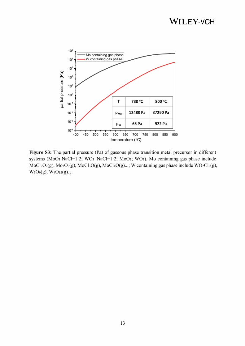
Figure S3: The partial pressure (Pa) of gaseous phase transition metal precursor in different systems (MoO3:NaCl=1:2; WO3 :NaCl=1:2; MoO3; WO3). Mo containing gas phase include MoCl2O2(g), Mo3O9(g), MoCl3O(g), MoCl4O(g)...; W containing gas phase include WO2Cl2(g), W3O9(g), W4O12(g)…
400 450 500 550 600 650 700 750 800 850 90010-4
10-3
10-2
10-1
100
101
102
103
104
105
temperature (oC)
part
ial p
ress
ure
(P
a)
Mo containing gas phase W containing gas phase

14
Table S1. Chemical species considered for the Mo-O-Cl-Na system (total 40 species) and the W-O-Cl-Na system (total 44 species)

15
Figure S4: (a) - (d) OM image of MoSe2-WSe2 lateral heterostructures on 300nm SiO2/Si
showing different types of morphologies/shape of the grown heterostructure crystals. False colors are used to obtain better contrast. The shape of TMD monolayer crystals are determined by the growth rate of different crystals faces which can be highly influenced by precursor concentration and hydrogen content.[30-32] Due to inhomogeneous distribution of the metal precursor, the random crystal shapes (triangular, star-like, hexagonal) can be found in different position of the substrate.[32]

16
Figure S5: Raman spectra recorded at the boundary of the MoSe2 and WSe2 domains in the
lateral heterostructure. The spectra show super imposition of the A1g peak of MoSe2 and WSe2.
The individual peaks are deconvoluted and shown in different colours.
200 220 240 260 280 300
inte
nsit
y (a
rb. u
.)
Raman shift (cm-1)
MoSe2WSe2
Raman shift (cm‐1)
intensity (counts)
17
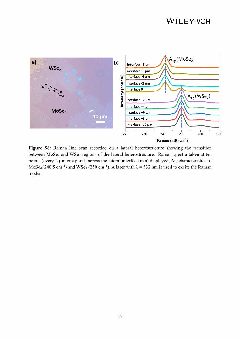
Figure S6: Raman line scan recorded on a lateral heterostructure showing the transition between MoSe2 and WSe2 regions of the lateral heterostructure. Raman spectra taken at ten points (every 2 µm one point) across the lateral interface in a) displayed, A1g characteristics of MoSe2 (240.5 cm–1) and WSe2 (250 cm–1). A laser with λ = 532 nm is used to excite the Raman modes.

18
Figure S7: XP spectra of as-grown monolayer MoSe2-WSe2 lateral heterostructures on SiO2/Si
substrate. The Se 3d (a), W 4f (b) and Mo 3d (c) spectra are shown. For better representation, the total intensities of Se 3d (a) and Mo 3d (c) spectra are multiplied by a factor of two. The Se 3d spectrum presented in (a) consists of a single species with a full width at half maximum (FWHM) of 0.9 eV at a binding energy (BE) of 54.5 eV (Se 3d5/2) and 55.4 eV (Se 3d3/2) due
to spin-orbit coupling. The W 4f spectrum shown in (b) consists of two doublets according to WSe2 at a BE of 32.6 eV (W 4f7/2, green, FWHM 0.7 eV) and to WO3 at a BE of 35.6 eV (W
4f7/2, blue, FWHM 1.5 eV). In addition, small contributions according to W 5p3/2 and Na 2s are
visible in the spectrum. Similarly, the Mo 3d spectrum in (c) also consists of the contribution due to MoSe2 at a BE of 228.4 eV (Mo 3d5/2, green, FWHM 0.8 eV) and MoO3 at a BE of 231.0
eV (Mo 3d5/2, blue, FWHM 2.2 eV). The spectrum overlaps with the contribution of the Se 3s
spectrum (229.3 eV, FWHM 1.8 eV, red). We calculated the elemental composition using the relative sensitivity factors of the respective peaks (Se 3d5/2 1.36, W 4f7/2 5.48, Mo 3d5/2 5.62)
and the ratio between the different species are determined as following: W:Mo:Se = 1.6±0.1 : 0.6±0.1 : 4±0.1 Mo + W : Se = 2.2±0.2 : 4±0.1. This confirms the high quality of the as-grown samples. By microscopically analysis we confirmed that the detected contribution of MoO3 and
WO3 are outside the grown heterostructures. Besides the here presented spectra, also Si 2p and
O 1s (substrate) as well as C 1s and Na 1s (from the used growth promotor) spectra were identified by the XPS analysis.

19
Figure S8: Localization of the MoSe2/WSe2 interface in 80 kV Cc/Cs-corrected HRTEM. (a)
shows an overview image of the lateral MoSe2 / WSe2 heterostructure with a defocus >100 µm.
Due to the huge defocus the interface (indicated by a faint red line) between WSe2 and MoSe2
can be identified. The white dotted line shows the edge of the whole flake. Furthermore, it is
striking that on the surface of the MoSe2 more prominent features can be seen, which in addition
helps to differentiate between MoSe2 and WSe2. These features are used to approach the
interface with increasing magnification. The blue squared area in (a) is shown in (b) and the
MoSe2 / WSe2 interface is again marked with the faint red line. Again, the blue-framed area in
(b) has been further magnified and is shown in (c) with the interface indicated by the red line.

20
Figure S9: (a) Device supercell of the p-n junction. The left electrode consists of columns of 2 units of MoSe2, the junction area consists of columns of 26 units of MoSe2 (only 6 shown) on the left and 26 units (only 6 shown) of WSe2 on the right, and the right electrode consists of columns of 2 units of WSe2. Blue atoms: Mo; Red atoms: W; Yellow atoms: S. (b) Photoresponse of an undoped junction calculated with DFT. The photoresponse has an onset at a photon energy of 2.35 eV (marked with the arrow). (c) Photoresponse of a doped junction with 2.6×10¹³ e/cm2 calculated with DFT. The onset for the doped junction is at 2.15 eV (marked with the arrow).

21
Figure S10: Band alignment of energy levels of lateral MoSe
2-WSe
2 lateral heterostructure
based on our optical/electrical measurements and reference 33.

22
Figure S11: (a) Rise and fall of photocurrent for the p-n junction device with Vds= 0 V and
without any applied gate voltage. (b) Rise and fall of photocurrent with an applied bias, Vds=
0.5 V and Vg = -20 V.
0 2 4 6 8 10
0.0
200.0
400.0
600.0
800.0
ss
I ds (p
A)
time (s)
nm
Vds
= 0.5 V
Vg= -20 V
14 16 18 20 22 24 26
0.0
50.0
100.0
150.0
200.0
250.0
300.0
350.0
I ds(
pA)
time (s)
ss
nm
Vds
= 0 V(a) (b)

23
Figure S12: Responsivity of the device as a function of applied source drain bias at Vg = 0 V.
-1.0 -0.5 0.0 0.5 1.0-100
-50
0
50
100
resp
onsi
vity
(m
A/W
)
Vds
(V)
intensity = 28 mW/cm2
520 nm
Vg = 0 V

24
Figure S13: OM images of as-grown monolayer MoSe2 (a) and WSe2 (b) crystals on 300nm SiO2/Si.
20 μm
(a)
20 μm
(b) MoSe2 WSe2

25
Figure S14: AFM height and phase image of as-grown monolayer MoSe
2 (a), (b) and
monolayer WSe2 (c),(d) on SiO2/Si substrate. The height profile between the SiO
2 substrate and
the TMD crystal is shown using solid white line (the height profiles are extracted from the dashed white lines). The thickness of the of monolayer MoSe
2 and monolayer WSe
2 are
estimated as 0.8±0.2 nm.
26
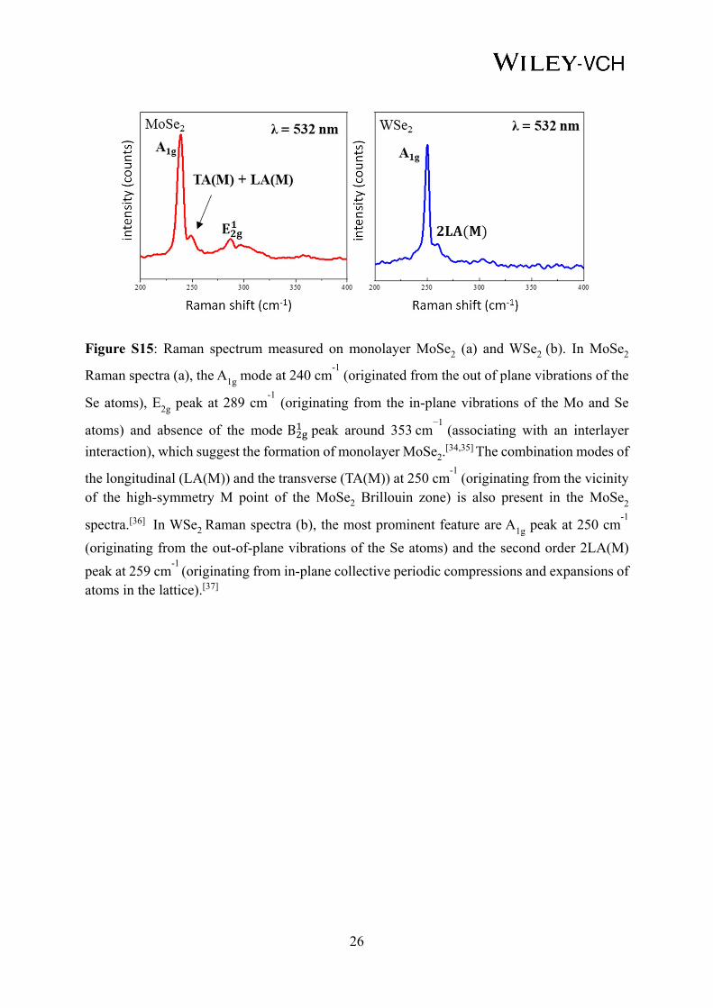
Figure S15: Raman spectrum measured on monolayer MoSe2 (a) and WSe2 (b). In MoSe2
Raman spectra (a), the A1g mode at 240 cm-1
(originated from the out of plane vibrations of the
Se atoms), E2g peak at 289 cm-1
(originating from the in-plane vibrations of the Mo and Se
atoms) and absence of the mode B peak around 353 cm−1
(associating with an interlayer
interaction), which suggest the formation of monolayer MoSe2.[34,35] The combination modes of
the longitudinal (LA(M)) and the transverse (TA(M)) at 250 cm-1
(originating from the vicinity of the high-symmetry M point of the MoSe2 Brillouin zone) is also present in the MoSe2
spectra.[36] In WSe2 Raman spectra (b), the most prominent feature are A1g peak at 250 cm-1
(originating from the out-of-plane vibrations of the Se atoms) and the second order 2LA(M)
peak at 259 cm-1
(originating from in-plane collective periodic compressions and expansions of atoms in the lattice).[37]

27
Figure S16: XP spectra of as-grown MoSe2 (a+b) and WSe2 (c+d) monolayers on SiO2/Si substrate. The Mo 3d (a), Se 3d (b+d) and W 4f (c) spectra are shown. For better representation, the total intensities of Se 3d and W 4f spectra are multiplied by a respective factor in the figure. The Mo 3d spectrum presented in (a) consists of the contribution due to MoSe2 at a BE of 229.0 eV (Mo 3d5/2, green, FWHM 0.7 eV) and MoO3 at a BE of 232.0 eV (Mo 3d5/2, blue, FWHM 2.0 eV). The spectrum overlaps with the contribution of the Se 3s spectrum (229.5 eV, FWHM 2.0 eV, red). The Se 3d spectrum presented in (b) consists of a single species with a full width at half maximum (FWHM) of 0.7 eV at a binding energy (BE) of 54.6 eV (Se 3d5/2) and 55.5 eV (Se 3d3/2) due to spin-orbit coupling. We calculated the elemental composition using the relative sensitivity factors of the respective peaks (Se 3d5/2 1.36, Mo 3d5/2 5.62) and determined it to Se:Mo = 1.8 : 1 ± 0.2. The W 4f spectrum shown in (c) consists of two doublets according to WSe2 at a BE of 32.5 eV (W 4f7/2, green, FWHM 0.6 eV) and to WO3 at a BE of 35.8 eV (W 4f7/2, blue, FWHM 1.7 eV). In addition, a small contribution according to W 5p3/2 is visible in the spectrum. The Se 3d spectrum presented in (d) consists of a single species with a full width at half maximum (FWHM) of 0.8 eV at a binding energy (BE) of 54.7 eV (Se 3d5/2) and a small peak according to Se loss features. The elemental composition is calculated using the relative sensitivity factors of the respective peaks (Se 3d5/2 1.36, W 4f7/2 5.48 and is determined to Se:W = 2.1 : 1 ± 0.2. This confirms the high quality of the as-grown samples. By microscopically analysis we confirmed that the detected contribution of MoO3 and WO3 are outside the grown monolayers. Besides the here presented spectra, also Si 2p and O 1s (substrate) as well as C 1s and Na 1s (from the used growth promotor) spectra were identified by the XPS analysis.

28
Figure S17: Electrical characterization of CVD grown MoSe2. (a) I-V characteristics of a MoSe2 device under dark and under illumination with 520 nm laser at an intensity of ~61 mW/cm2. However, the device does not show any rectification behaviour or photovoltaic effect as observed in the lateral heterostructure p-n junction devices. (b) The transfer characteristics of the device with an applied gate sweep from -50V to 50 V at Vds = 0.1V. The device shows the n-type transport behaviour with estimated field effect electron mobility of 25 cm2/Vs.

29
Figure S18: Electrical characterization of CVD grown WSe2. (a) I-V characteristics of a WSe2 device under dark and under illumination with 520 nm laser at an intensity of ~61 mW/cm2. However, the device does not show any rectification behaviour or photovoltaic effect as observed in the lateral heterostructure p-n junction devices. (b) The transfer characteristics of the device with an applied gate sweep from -50 V to 50 V at Vds = 1 V. The device showing the p-type transport behaviour with estimated field effect hole mobility of 0.012 cm2/Vs.
30
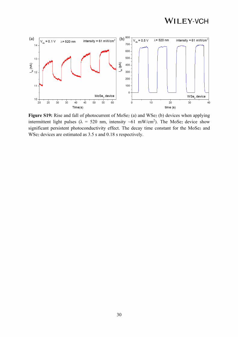
Figure S19: Rise and fall of photocurrent of MoSe2 (a) and WSe2 (b) devices when applying intermittent light pulses (λ = 520 nm, intensity ~61 mW/cm2). The MoSe2 device show significant persistent photoconductivity effect. The decay time constant for the MoSe2 and WSe2 devices are estimated as 3.5 s and 0.18 s respectively.

31
REFERENCES [1] A. Turchanin, A. Beyer, C. T. Nottbohm, X. Zhang, R. Stosch, A. Sologubenko, J.
Mayer, P. Hinze, T. Weimann, A. Gölzhäuser, Adv. Mater. 2009, 21, 1233.
[2] M. Linck, P. Hartel, S. Uhlemann, F. Kahl, H. Müller, J. Zach, M. Haider, M. Niestadt,
M. Bischoff, J. Biskupek, Z. Lee, T. Lehnert, F. Börrnert, H. Rose, U. Kaiser, Phys. Rev. Lett.
2016, 117, 076101.
[3] S. Smidstrup, T. Markussen, P. Vancraeyveld, J. Wellendorff, J. Schneider, T. Gunst,
B. Verstichel, D. Stradi, P. A. Khomyakov, U. G. Vej-Hansen, M.-E. Lee, S. T. Chill, F.
Rasmussen, G. Penazzi, F. Corsetti, A. Ojanperä, K. Jensen, M. L. N. Palsgaard, U. Martinez,
A. Blom, M. Brandbyge, K. Stokbro, J. Phys. Condens. Matter. 2019, 32, 015901.
[4] S. Smidstrup, D. Stradi, J. Wellendorff, P. A. Khomyakov, U. G. Vej-Hansen, M.-E.
Lee, T. Ghosh, E. Jónsson, H. Jónsson, K. Stokbro, Phys. Rev. B. 2017, 96, 195309.
[5] M. J. van Setten, M. Giantomassi, E. Bousquet, M. J. Verstraete, D. R. Hamann, X.
Gonze, G. M. Rignanese, Comput. Phys. Commun. 2018, 226, 39.
[6] J. P. Perdew, Y. Wang, Phys. Rev. B. 1992, 45, 13244.
[7] S. Lei, X. Wang, B. Li, J. Kang, Y. He, A. George, L. Ge, Y. Gong, P. Dong, Z. Jin, G.
Brunetto, W. Chen, Z.-T. Lin, R. Baines, D. S. Galvão, J. Lou, E. Barrera, K. Banerjee, R.
Vajtai, P. Ajayan, Nat. Nanotechnol. 2016, 11, 465.
[8] A. George, C. Neumann, D. Kaiser, R. Mupparapu, T. Lehnert, U. Hübner, Z. Tang, A.
Winter, U. Kaiser, I. Staude, A. Turchanin, J. Phys. Mater. 2019, 2, 016001.
[9] D. Zhou, H. Shu, C. Hu, L. Jiang, P. Liang, X. Chen, Cryst. Growth. Des. 2018, 18, 1012.
[10] T. H. Swan, E. Mack, J. Am. Chem. Soc. 1925, 47, 2112.
[11] L. S. Brooks, J. Am. Chem. Soc. 1952, 74, 227.
[12] P. Clausing, Annalen der Physik 1932, 406, 134.
[13] B. Zheng, Y. Chen, IOP Conf. Ser.: Mater. Sci. Eng. 2017, 274, 012085.
[14] B. Liu, M. Fathi, L. Chen, A. Abbas, Y. Ma, C. Zhou, ACS Nano. 2015, 9, 6119.
[15] W. Y. Lee, T. M. Besmann, M. W. Stott, J. Mater. Res. 1994, 9, 1474.
[16] V. Kranthi Kumar, S. Dhar, T. H. Choudhury, S. A. Shivashankar, S. Raghavan,
Nanoscale 2015, 7, 7802.
[17] T. H. Choudhury, H. Simchi, R. Boichot, M. Chubarov, S. E. Mohney, J. M. Redwing,
Cryst. Growth. Des. 2018, 18, 4357.
[18] K. V. Manukyan, K. G. Kirakosyan, Y. G. Grigoryan, O. M. Niazyan, A. V. Yeghishyan,
A. G. Kirakosyan, S. L. Kharatyan, Ind. Eng. Chem. Res. 2011, 50, 10982.
[19] M. Mobin, Sci. Eng. Compos. Mater. 1999, 8, 257.

32
[20] S. M. Delphine, M. Jayachandran, C. Sanjeeviraja, MRS Bull. 2005, 40, 135.
[21] W. J. Schutte, J. L. De Boer, F. Jellinek, J. Solid State Chem.1987, 70, 207.
[22] R. Leiter, Y. Li, U. Kaiser, Nanotechnology 2020, 31, 495704.
[23] T. Lehnert, O. Lehtinen, G. Algara–Siller, U. Kaiser, Appl. Phys. Lett. 2017, 110, 033106.
[24] M. Lentzen, Microsc. Microanal. 2008, 14, 16.
[25] M. Palsgaard, T. Markussen, T. Gunst, M. Brandbyge, K. Stokbro, Phys. Rev. Appl.
2018, 10, 014026.
[26] C. Zhang, C. Gong, Y. Nie, K.-A. Min, C. Liang, Y. J. Oh, H. Zhang, W. Wang, S.
Hong, L. Colombo, R. M. Wallace, K. Cho, 2D Mater. 2016, 4, 015026.
[27] O. Lopez-Sanchez, D. Lembke, M. Kayci, A. Radenovic, A. Kis. Nat. Nanotechnol,
2013, 8, 497–501.
[28] Y.-C. Wu, C.-H. Liu, S.-Y. Chen, F.-Y. Shih, P.-H. Hp, C.W. Chen, C.-T. Liang, W.-H.
Wang. Sci. Rep. 2015, 5, 11472.
[29] A. George, M.V. Fistul, M. Gruenewald, D. Kaiser, T. Lehnert, R. Mupparapu, C.
Neumann, U. Hübner, M. Schaal, N. Masurkar, L. M. R. Arava, I. Staude, U. Kaiser, T. Fritz,
A. Turchanin, npj 2D Mater. Appl. 2021, 5, 15.
[30] X. Zhang, H. Nan, S. Xiao, X. Wan, Z. Ni, X. Gu, K. Ostrikov, ACS Appl. Mater.
Interfaces. 2017, 9, 42121.
[31] Y. Li, F. Wang, D. Tang, J. Wei, Y. Li, Y. Xing, K. Zhang, Mater. Lett. 2018, 216,
261.
[32] S. Chowdhury, A. Roy, I. Bodemann, S. K. Banerjee, ACS Appl. Mater. Interfaces
2020, 12, 15885.
[33] J. R. Durán Retamal, D. Periyanagounder, J.-J. Ke, M.-L. Tsai, J.-H. He, Chem. Sci.
2018, 9, 7727.
[34] P. Tonndorf, R. Schmidt, P. Böttger, X. Zhang, J. Börner, A. Liebig, M. Albrecht, C. Kloc,
O. Gordan, D. R. T. Zahn, S. M. de Vasconcellos, R. Bratschitsch, Opt. Express. 2013, 21, 4908-
4916.
[35] M. Yang, X. Cheng, Y. Li, Y. Ren, M. Liu, Z. Qi, Appl. Phys. Lett. 2017, 110, 093108.
[36] P. Soubelet, A. E. Bruchhausen, A. Fainstein, K. Nogajewski, C. Faugeras, Phys. Rev.
B. 2016, 93, 155407.
[37] J.-K. Huang, J. Pu, C.-L. Hsu, M.-H. Chiu, Z.-Y. Juang, Y.-H. Chang, W.-H. Chang, Y.
Iwasa, T. Takenobu, L.-J. Li, ACS Nano. 2014, 8, 923.