Giant Polarization Sustainability in Ultrathin Ferroelectric … · 2017 WILEY-VCH Verlag GmbH &...
10
COMMUNICATION 1703543 (1 of 10) © 2017 WILEY-VCH Verlag GmbH & Co. KGaA, Weinheim www.advmat.de Giant Polarization Sustainability in Ultrathin Ferroelectric Films Stabilized by Charge Transfer Sirui Zhang, Yinlian Zhu,* Yunlong Tang, Ying Liu, Shuang Li, Mengjiao Han, Jinyuan Ma, Bo Wu, Zuhuang Chen, Sahar Saremi, and Xiuliang Ma* S. R. Zhang, Prof. Y. L. Zhu, Dr. Y. L. Tang, Dr. Y. Liu, S. Li, M. J. Han, J. Y. Ma, B. Wu, Prof. X. L. Ma Shenyang National Laboratory for Materials Science Institute of Metal Research Chinese Academy of Sciences Wenhua Road 72, 110016 Shenyang, China E-mail: [email protected]; [email protected] S. R. Zhang, Dr. Y. Liu, S. Li, M. J. Han University of Chinese Academy of Sciences Yuquan Road 19, 100049 Beijing, China J. Y. Ma, Prof. X. L. Ma School of Materials Science and Engineering Lanzhou University of Technology Langongping Road 287, 730050 Lanzhou, China Dr. Z. H. Chen, S. Saremi Department of Materials Science and Engineering University of California Berkeley, CA 94720, USA Dr. Z. H. Chen Materials Science Division Lawrence Berkeley National Laboratory Berkeley, CA 94720, USA DOI: 10.1002/adma.201703543 Interface engineering of oxides, which is based on a control of layer-by-layer growth for a heteroepitaxial system across the interface, is known to be able to induce novel physical phenomenon at the inter- face such as, 2D electron gas [1,2] and magnetoelectric coupling effect. [3,4] Fer- roelectric oxides, featuring asymmetric or polar structures that are switchable under an external field, are required to take the form of nanoscale films in future electronic devices. Although ultrathin films of BaTiO 3 and Pb(Zr x ,Ti 1–x )O 3 (PZT) are expected to show a permanent switchable spontaneous polarization and hold promise in ferro- electric random access memory, ferroelec- tric field-effect transistors, and sensors, [5–7] it is generally believed that the interface- induced depolarization field strongly dete- riorate the ferroelectricity when the films are downsized to unit cell scale. [8–11] For instance, theoretical studies indicate that the residual depolarization field leads to incomplete compensation charge in ferro- electric films and the critical thickness is proposed below which ferroelectric polar state is unstable or even vanishes. [12–14] The critical thickness obtained by theoretical methods generally ranges from 10 to 40 Å. [15–17] Experimentally, by a combination of electron microscopy and piezoelectric microscopy, an earlier experimental study shows a stable ferroelectric polarization in 40 Å thick Pb(Zr 0.2 Ti 0.8 )O 3 films. [18] Later on, switchable polari- zation 11 µC cm −2 was measured in 40 Å Pb(Zr 0.2 Ti 0.8 )O 3 film, which is the ultrathin PZT film exhibiting switchable polariza- tions. [19] Nevertheless, this polarization is much decreased as compared with bulk Pb(Zr 0.2 Ti 0.8 )O 3 where ≈80 µC cm −2 can be obtained. In PbTiO 3 , high resolution X-ray study indicates that the presence of a residual unscreened depolarizing field may result in a critical size of 24 Å and significantly reduced polarization of ≈25 µC cm −2 was deduced, which corresponds to a 70% reduction compared with bulk PbTiO 3 . [20] While using synchrotron X-ray technique, Fong et al. found periodic 180° domains in PbTiO 3 films down to 3 unit cells (12 Å) at room temperature. [21] Very recently, Gao et al. proposed that a critical thickness for ferroelectricity in ultrathin films may be absent and they found the polarization of about 16 µC cm −2 in a 1.5 unit cell thick PbZr 0.2 Ti 0.8 O 3 film grown on SrTiO 3 and 22 µC cm −2 in a 2 unit cell thick film with a SrRuO 3 electrode Ferroelectricity is generally deteriorated or even vanishes when the ferro- electric films are downsized to unit cell scale. To maintain and enhance the polarization in nanoscale ferroelectrics are of scientific and technological importance. Here, giant polarization sustainability is reported in a series of ultrathin PbTiO 3 films scaled down to three unit cells grown on NdGaO 3 (110) substrates with La 0.7 Sr 0.3 MnO 3 as bottom electrodes. Atomic mappings via aberration-corrected scanning transmission electron microscopy demonstrate the robust ferroelectricity for the sub-10 nm thick film. For the 1.2 nm thick film, the polarization reaches ≈50 µC cm −2 . The 2 nm thick film possesses a polarization as high as the bulk value. The films ranging from 10 to 35 nm display a giant elongation of out-of-plane lattice parameter, which corre- sponds to a polarization of 100 µC cm −2 , 20% larger than that of the bulk PbTiO 3 . The giant enhancement of polarization in the present films is pro- posed to result from the charge transfer at the La 0.7 Sr 0.3 MnO 3 /PbTiO 3 inter- face, as supported by the anomalous decrease of Mn valence measured from X-ray photoelectron spectroscopy. These results reveal the significant role of charge transfer at interfaces in improving large polarizations in ultrathin ferroelectrics and are meaningful for the development of future electronic devices. Ferroelectricity Enhancement Adv. Mater. 2017, 1703543
Transcript of Giant Polarization Sustainability in Ultrathin Ferroelectric … · 2017 WILEY-VCH Verlag GmbH &...
CommuniCation
1703543 (1 of 10) © 2017 WILEY-VCH Verlag GmbH & Co. KGaA, Weinheim
www.advmat.de
Giant Polarization Sustainability in Ultrathin Ferroelectric Films Stabilized by Charge Transfer
Sirui Zhang, Yinlian Zhu,* Yunlong Tang, Ying Liu, Shuang Li, Mengjiao Han, Jinyuan Ma, Bo Wu, Zuhuang Chen, Sahar Saremi, and Xiuliang Ma*
S. R. Zhang, Prof. Y. L. Zhu, Dr. Y. L. Tang, Dr. Y. Liu, S. Li, M. J. Han, J. Y. Ma, B. Wu, Prof. X. L. MaShenyang National Laboratory for Materials ScienceInstitute of Metal ResearchChinese Academy of SciencesWenhua Road 72, 110016 Shenyang, ChinaE-mail: [email protected]; [email protected]. R. Zhang, Dr. Y. Liu, S. Li, M. J. HanUniversity of Chinese Academy of SciencesYuquan Road 19, 100049 Beijing, ChinaJ. Y. Ma, Prof. X. L. MaSchool of Materials Science and EngineeringLanzhou University of TechnologyLangongping Road 287, 730050 Lanzhou, ChinaDr. Z. H. Chen, S. SaremiDepartment of Materials Science and EngineeringUniversity of CaliforniaBerkeley, CA 94720, USADr. Z. H. ChenMaterials Science DivisionLawrence Berkeley National LaboratoryBerkeley, CA 94720, USA
DOI: 10.1002/adma.201703543
Interface engineering of oxides, which is based on a control of layer-by-layer growth for a heteroepitaxial system across the interface, is known to be able to induce novel physical phenomenon at the inter-face such as, 2D electron gas[1,2] and magnetoelectric coupling effect.[3,4] Fer-roelectric oxides, featuring asymmetric or polar structures that are switchable under an external field, are required to take the form of nanoscale films in future electronic devices. Although ultrathin films of BaTiO3 and Pb(Zrx,Ti1–x)O3 (PZT) are expected to show a permanent switchable spontaneous polarization and hold promise in ferro-electric random access memory, ferroelec-tric field-effect transistors, and sensors,[5–7] it is generally believed that the interface-induced depolarization field strongly dete-riorate the ferroelectricity when the films are downsized to unit cell scale.[8–11] For instance, theoretical studies indicate that the residual depolarization field leads to incomplete compensation charge in ferro-electric films and the critical thickness is proposed below which ferroelectric polar state is unstable or even vanishes.[12–14]
The critical thickness obtained by theoretical methods generally ranges from 10 to 40 Å.[15–17] Experimentally, by a combination of electron microscopy and piezoelectric microscopy, an earlier experimental study shows a stable ferroelectric polarization in 40 Å thick Pb(Zr0.2Ti0.8)O3 films.[18] Later on, switchable polari-zation 11 µC cm−2 was measured in 40 Å Pb(Zr0.2Ti0.8)O3 film, which is the ultrathin PZT film exhibiting switchable polariza-tions.[19] Nevertheless, this polarization is much decreased as compared with bulk Pb(Zr0.2Ti0.8)O3 where ≈80 µC cm−2 can be obtained. In PbTiO3, high resolution X-ray study indicates that the presence of a residual unscreened depolarizing field may result in a critical size of 24 Å and significantly reduced polarization of ≈25 µC cm−2 was deduced, which corresponds to a 70% reduction compared with bulk PbTiO3.[20] While using synchrotron X-ray technique, Fong et al. found periodic 180° domains in PbTiO3 films down to 3 unit cells (12 Å) at room temperature.[21] Very recently, Gao et al. proposed that a critical thickness for ferroelectricity in ultrathin films may be absent and they found the polarization of about 16 µC cm−2 in a 1.5 unit cell thick PbZr0.2Ti0.8O3 film grown on SrTiO3 and 22 µC cm−2 in a 2 unit cell thick film with a SrRuO3 electrode
Ferroelectricity is generally deteriorated or even vanishes when the ferro-electric films are downsized to unit cell scale. To maintain and enhance the polarization in nanoscale ferroelectrics are of scientific and technological importance. Here, giant polarization sustainability is reported in a series of ultrathin PbTiO3 films scaled down to three unit cells grown on NdGaO3(110) substrates with La0.7Sr0.3MnO3 as bottom electrodes. Atomic mappings via aberration-corrected scanning transmission electron microscopy demonstrate the robust ferroelectricity for the sub-10 nm thick film. For the 1.2 nm thick film, the polarization reaches ≈50 µC cm−2. The 2 nm thick film possesses a polarization as high as the bulk value. The films ranging from 10 to 35 nm display a giant elongation of out-of-plane lattice parameter, which corre-sponds to a polarization of 100 µC cm−2, 20% larger than that of the bulk PbTiO3. The giant enhancement of polarization in the present films is pro-posed to result from the charge transfer at the La0.7Sr0.3MnO3/PbTiO3 inter-face, as supported by the anomalous decrease of Mn valence measured from X-ray photoelectron spectroscopy. These results reveal the significant role of charge transfer at interfaces in improving large polarizations in ultrathin ferroelectrics and are meaningful for the development of future electronic devices.
Ferroelectricity Enhancement
Adv. Mater. 2017, 1703543
© 2017 WILEY-VCH Verlag GmbH & Co. KGaA, Weinheim1703543 (2 of 10)
www.advmat.dewww.advancedsciencenews.com
by means of Cs-corrected transmission electron microscopy.[22] In addition, for ≈20 Å BaTiO3 films, switchable polarizations were obtained and high performance ferroelectric tunnel junc-tions were thus fabricated.[23–28] The results above suggest that the critical thicknesses for ferroelectric films might be much thinner than theoretical suggestions or even vanish. Neverthe-less, both theoretical and experimental results indicate that fer-roelectricity can be largely restrained within unit cell scales.
Although great efforts have been made to figure out the polarization behavior in ultrathin ferroelectric films, so far there is still great obstacle preventing large polarization and its sustainability in ultrathin ferroelectric films. It is proposed that the spontaneous polarization in ultrathin ferroelectrics can be improved by compression strains.[29,30] It is also pre-dicted that the polarization in ultrathin PbTiO3 films may be enhanced by chemically modified stiffness of the ferroelectric/electrode bond at interfaces of metal and oxide from first-prin-ciples calculations.[31] Very recently, by tailoring the interface engineering, the polarization in PbTiO3 layer can be greatly increased at PbTiO3/BiFeO3 bilayers grown on SrTiO3 sub-strates, which attributes to the oxygen vacancy accumulation at PbTiO3/BiFeO3 interfaces.[32] In addition, oxygen vacancy is found to play an important role in improving the polarization in BaTiO3 films grown on SrTiO3 substrates as well.[33]
Here, we report giant polarization sustainability in ultrathin PbTiO3 (PTO) films scaled down to several unit cells. PTO films with the thicknesses of 1.2, 2, 3.6, 6, 10, 15, and 35 nm were grown on the conductive La0.7Sr0.3MnO3 (LSMO, ≈8 nm) buffered NdGaO3 (110) (NGO) substrates by pulsed laser depo-sition (PLD) technique. We apply high angle annular dark field (HAADF) imaging, piezoelectric force microscopy (PFM) and X-ray photoelectron spectroscopic (XPS) technique to clarify the atomic-scale structural details, polarization behaviors, and chemical valence in a series of PTO films with the thickness down to three unit cells.
PTO exhibits tetragonal symmetry at room temperature with lattice parameters of a = b = 3.904 Å and c = 4.158 Å.[34] In PTO unit cell, both oxygen octahedron and Ti4+ have a shift from the mass center of the Pb2+ lattice, generating a spontaneous polarization (Ps) along [001] direction. The reversed displace-ment direction of Ti4+ can decide the polarization orientation of the PTO film.[35] [110]O NGO substrate (the subscript O indi-cates orthorhombic) has an orthorhombic structure exhibiting a pseudocubic lattice parameter of about 3.861 Å.[36] In this work, the [110]O NGO substrate delivers a compressive strain to PTO by ≈1.0% ((afilm − asubstrate)/afilm ≈ 1.0%). Conductive LSMO[37] is chosen as the bottom electrode trying to compensate the polarization-induced bound charge, and the mismatch between LSMO and NGO is as small as 0.3%.
Figure 1a is a low-magnification HAADF-scanning trans-mission electron microscopy (STEM) image showing the 3.6 nm thick PTO buffered with a LSMO layer. The white arrows denote the interfaces of NGO/LSMO and LSMO/PTO, where the sharp and flat interfaces are clearly displayed. To demonstrate the ion displacements, an enlarged pattern corre-sponding to the area outlined with a red square is shown in Figure 1b, c axis oriented PTO unit cells can be deduced here. Opposite to the direction of Ti displacement, the direction of spontaneous polarization (Ps) vector in the PTO film is upward;
this polarization direction is consistent with previous reports in the PZT film with a LSMO bottom electrode, where the upward polarization is induced by different work functions between LSMO and PTO.[38] In order to see the strain distribution inside the film and also at the interfaces, geometric phase analysis (GPA)[39,40] is performed and the result is shown in Figure 1c. It is clearly seen that the PTO has larger out of plane strains com-pared to NGO. A line profile along the blue line in Figure 1c is displayed in Figure 1d, where the increase of strains in the PTO layer is remarkable and a peak appears at the PTO/LSMO interface (marked with a green arrow).
For such a ultrathin film and film/electrode interface, tradi-tional electrical measurements are hard to study the ferroelec-tric response at atomic scale.[18,22,41] Alternatively, by means of aberration-corrected scanning transmission electron micros-copy (Cs-corrected STEM imaging),[42] we can easily obtain the atomic information of ultrathin films.[8,35] Figure 1e is an atomic resolved HAADF-STEM image showing the interface of the 3.6 nm thick PTO film. The white arrows denote the LSMO/PTO interface. The atomic column positions are deter-mined by 2D Gaussian fitting[43,44] and corrected by the sub-strate parameters. The map of the out-of-plane (c axis) lattice spacing obtained from Figure 1e is shown in Figure 1f. Note that the PTO has an interfacial region featuring the localized increase of the out-of-plane lattice spacings. Figure 1g shows the statistics results for the lattice parameters of a and c, and the calculated tetragonality is shown in Figure 1h. We find that both c and a for the LSMO layer maintain a constant value up to the interface. The in-plane lattice parameter (Figure 1g) of the PTO film is nearly unchanged and maintains with the lattice parameter of NGO, as marked with a red arrow. In contrast, the out-plane lattice parameter c of the PTO layer increases gradu-ally and reaches a maximum at the position near the PTO film surface. The tetragonality shows essentially the same behavior as the c axis lattice parameter. Both c parameter and tetrago-nality exhibit an increase trend from the interfacial peak to the surface, where the peak values are marked with green arrows in Figure 1g,h, respectively. The c lattice reaches a value of 4.3 Å in the film surface, and the in-plane lattice parameter a of PTO adopts that of NGO (a = 3.861 Å), and then the tetragonality value of PTO is calculated as c/a ≈ 1.11. This value is consider-ably larger than the bulk value of 1.065. Although the tetrago-nality should increase because of the compression strain,[29,30] the large tetragonality value in this film system far exceeds the maximum modified by strains (will be discussed in later in Equations (2)–(4)). Due to the strongly coupling of strains and polarizations for PTO,[20,45] there also exists a large spontaneous polarization in this ultrathin film. This polarization enhance-ment is accompanied with the interface lattice elongation which also strongly supports a giant polarization enhancement near the interface.
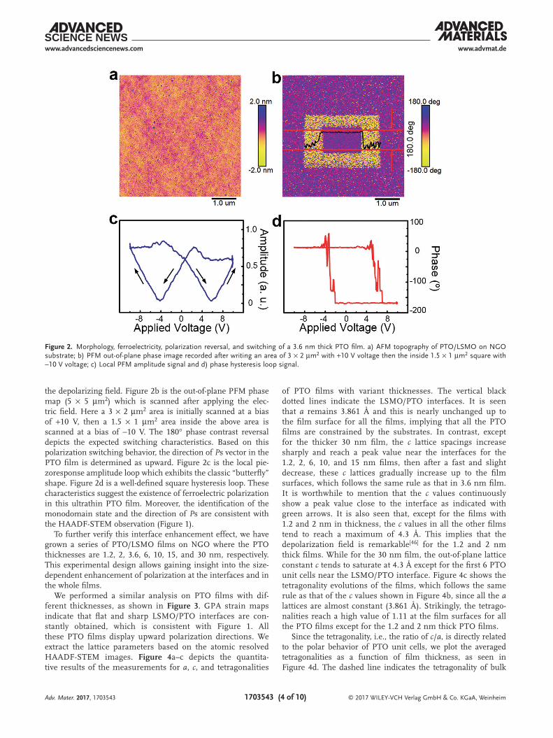
In order to find the ferroelectricity nature of this film, PFM is applied. First the surface topography of the as-grown film is investigated using atomic force microscopy, as shown in Figure 2a. It is seen that the LSMO/PTO heterostruc-ture is atomically flat over an area of 5 × 5 µm2 with a root-mean-square surface roughness of ≈0.20 nm. PFM analysis indicates that the PTO film is in a single-domain state with out-of-plane polarization, implying an effective screening of
Adv. Mater. 2017, 1703543

© 2017 WILEY-VCH Verlag GmbH & Co. KGaA, Weinheim1703543 (3 of 10)
www.advmat.dewww.advancedsciencenews.com
Adv. Mater. 2017, 1703543
Figure 1. a) A cross-sectional low-magnification high resolution HAADF-STEM image of PTO(3.6 nm)/LSMO/NGO(110). The horizontal white arrows denote the interfaces of LSMO/PTO and LSMO/NGO, respectively; b) An enlarged HAADF-STEM image from the red box of (a) showing the displace-ment direction of the Ti atoms. The spontaneous polarization Ps direction, which is opposite to δTi, is denoted by the vertical arrow. c) GPA analysis for (a) revealing the distribution of the out-of-plane strain εyy; d) The strain profile corresponding to the blue line in (c). The green arrow indicates the enlargement of the strain at the interface. e) An atomic resolved HAADF-STEM image showing the PTO/LSMO interface; f) Corresponding out-of-plane lattice spacing map for (e). The horizontal white arrows in (e) and (f) indicate the position of the interface; g) Lattice parameter c and a; and h) tetragonality as a function of the unit cell distance from LSMO to PTO derived from (e). The red arrow in (g) denotes the lattice parameters of NGO. The green arrows in (g) and (h) indicate the enlargement of the lattice and c/a at the interface (yellow circle: Pb; red circle: Ti; green circle: La(Sr); purple circle: Mn.)
© 2017 WILEY-VCH Verlag GmbH & Co. KGaA, Weinheim1703543 (4 of 10)
www.advmat.dewww.advancedsciencenews.com
the depolarizing field. Figure 2b is the out-of-plane PFM phase map (5 × 5 µm2) which is scanned after applying the elec-tric field. Here a 3 × 2 µm2 area is initially scanned at a bias of +10 V, then a 1.5 × 1 µm2 area inside the above area is scanned at a bias of −10 V. The 180° phase contrast reversal depicts the expected switching characteristics. Based on this polarization switching behavior, the direction of Ps vector in the PTO film is determined as upward. Figure 2c is the local pie-zoresponse amplitude loop which exhibits the classic “butterfly” shape. Figure 2d is a well-defined square hysteresis loop. These characteristics suggest the existence of ferroelectric polarization in this ultrathin PTO film. Moreover, the identification of the monodomain state and the direction of Ps are consistent with the HAADF-STEM observation (Figure 1).
To further verify this interface enhancement effect, we have grown a series of PTO/LSMO films on NGO where the PTO thicknesses are 1.2, 2, 3.6, 6, 10, 15, and 30 nm, respectively. This experimental design allows gaining insight into the size-dependent enhancement of polarization at the interfaces and in the whole films.
We performed a similar analysis on PTO films with dif-ferent thicknesses, as shown in Figure 3. GPA strain maps indicate that flat and sharp LSMO/PTO interfaces are con-stantly obtained, which is consistent with Figure 1. All these PTO films display upward polarization directions. We extract the lattice parameters based on the atomic resolved HAADF-STEM images. Figure 4a–c depicts the quantita-tive results of the measurements for a, c, and tetragonalities
of PTO films with variant thicknesses. The vertical black dotted lines indicate the LSMO/PTO interfaces. It is seen that a remains 3.861 Å and this is nearly unchanged up to the film surface for all the films, implying that all the PTO films are constrained by the substrates. In contrast, except for the thicker 30 nm film, the c lattice spacings increase sharply and reach a peak value near the interfaces for the 1.2, 2, 6, 10, and 15 nm films, then after a fast and slight decrease, these c lattices gradually increase up to the film surfaces, which follows the same rule as that in 3.6 nm film. It is worthwhile to mention that the c values continuously show a peak value close to the interface as indicated with green arrows. It is also seen that, except for the films with 1.2 and 2 nm in thickness, the c values in all the other films tend to reach a maximum of 4.3 Å. This implies that the depolarization field is remarkable[46] for the 1.2 and 2 nm thick films. While for the 30 nm film, the out-of-plane lattice constant c tends to saturate at 4.3 Å except for the first 6 PTO unit cells near the LSMO/PTO interface. Figure 4c shows the tetragonality evolutions of the films, which follows the same rule as that of the c values shown in Figure 4b, since all the a lattices are almost constant (3.861 Å). Strikingly, the tetrago-nalities reach a high value of 1.11 at the film surfaces for all the PTO films except for the 1.2 and 2 nm thick PTO films.
Since the tetragonality, i.e., the ratio of c/a, is directly related to the polar behavior of PTO unit cells, we plot the averaged tetragonalities as a function of film thickness, as seen in Figure 4d. The dashed line indicates the tetragonality of bulk
Adv. Mater. 2017, 1703543
Figure 2. Morphology, ferroelectricity, polarization reversal, and switching of a 3.6 nm thick PTO film. a) AFM topography of PTO/LSMO on NGO substrate; b) PFM out-of-plane phase image recorded after writing an area of 3 × 2 µm2 with +10 V voltage then the inside 1.5 × 1 µm2 square with −10 V voltage; c) Local PFM amplitude signal and d) phase hysteresis loop signal.

© 2017 WILEY-VCH Verlag GmbH & Co. KGaA, Weinheim1703543 (5 of 10)
www.advmat.dewww.advancedsciencenews.com
PTO. It is seen that the c/a ratio decreases substantially for the films less than 6 nm. However, for the PTO films thicker than 1.2 nm, their c/a ratios are still much larger than the bulk PTO. Particularly, when the film thickness is over 10 nm, the c/a ratio stops increasing and maintains the value of 1.1. It is worthwhile to mention that the tetragonality in the 1.2 nm film is relatively large compared with that previously reported.[20,22] Since the evolution of tetragonality is strongly associated with the spontaneous polarization (Ps) through the strain-polari-zation coupling,[20,45] we derive the polarization from c-lattice parameters based on the Landau–Ginzburg–Devonshire phe-nomenological theory[47] by Equation (1)
Px s s s x
Q s s s Q= − +
− +
s
(2 /( ))
(2 /( ))3 12 11 12 m
11 12 11 12 12
1/2
(1)
where Qij are electrostriction coefficients. sij are elastic com-pliances; b is the extrapolated lattice parameter of the cubic paraelectric phase; x3 and xm are the out-of-plane and in-plane
strains defined with x3 = (c − b)/b and xm = (a − b)/b, respectively. In the present system, the c values are measured according to the atomic images and a is the lattice parameter of NGO because of the strain impingement on the films. The values of Qij, sij, and b for PTO are taken from refs. [47,48]. It is noted that phenomenological approach based on the Landau–Ginz-burg–Devonshire theory is proved to be effective in estimating ferroelectric behaviors.[49] The spontaneous polarizations are then derived and shown in Figure 4e, where the value of bulk PTO (≈84 µC cm−2, derived also from the equation above) is indicated with a dashed line. The curve of the evolution of the spontaneous polarizations is the same as that of the tetrago-nality (Figure 4d). It is seen that the Ps in 1.2 nm film exhibits a magnitude of about 50 µC cm−2. The Ps increases with the film thicknesses from 1.2, 2, 3.6, 6, to 10 nm, giving rise to a max-imum value of 100 µC cm−2 for PTO film thicker than 10 nm, which is 20% larger than that of the bulk. The P–E hysteresis loop for the 30 nm PTO film is displayed in Figure S1 (Sup-porting Information), which evidently shows the large polariza-tion in spite of the leakage.
Adv. Mater. 2017, 1703543
Figure 3. Low-magnification HAADF-STEM images of PTO/LSMO/NGO(110) films with the thickness of PTO for a) 1.2, b) 2, c) 6, d) 10, e) 15, and f) 30 nm. g–l) The corresponding GPA analysis of out-of-plane normal strain εyy for (a–f). White arrows indicate heterointerfaces in these photographs.

© 2017 WILEY-VCH Verlag GmbH & Co. KGaA, Weinheim1703543 (6 of 10)
www.advmat.dewww.advancedsciencenews.com
It is generally known that the Ps is strongly suppressed in ultrathin films,[15–21] however, in present study, the Ps values in the ultrathin films are quite large. If a PTO film receives a 1% strain from the NGO substrate, theoretical c should be 4.2 Å based on Equations (2–4)[50]
a a
axx yyε ε ε= = = − ≈ −0.01PTO
0
PTO0
(2)
v
vzzε ε= −
−≈2
10.01
(3)
Meantime, εzz is related to the out-of-plane strain of the PTO film, the out-of-plane lattice parameter c can be calculated using Equation (4)
c c
czzε = − PTO
0
PTO0
(4)
where εxx and εyy are the in-plane components of the misfit strain. a is the constrained lattice parameter of NGO substrate. aPTO
0 , cPTO0 are the bulk lattice parameters of PTO. εzz is out-of-
plane component of the misfit strain. v is the Poisson’s ratio which is equal to 0.33.[51] The calculated c value under the strain
Adv. Mater. 2017, 1703543
Figure 4. Extraction of corresponding lattice constants and tetragonality from different thick PTO film, and deduced evolution of both tetragonality and spontaneous polarization versus film thickness. a) Lattice parameter a, b) Lattice parameter c, and c) Tetragonality profiles as a function of the unit cell distance from LSMO to PTO. The green arrows indicate the enlargement of the c/a at the LSMO/PTO interface. d) Evolution of c/a ratio with film thickness; e) Evolution of the spontaneous polarization with film thickness. The spontaneous polarizations are derived from c-lattice parameters based on Landau–Ginzburg–Devonshire theory.

© 2017 WILEY-VCH Verlag GmbH & Co. KGaA, Weinheim1703543 (7 of 10)
www.advmat.dewww.advancedsciencenews.com
of NGO is thus 4.2 Å, which is smaller than the experimental value of 4.3 Å observed here. As a result, besides the strain from NGO, some other factors are supposed to contribute to the enhanced tetragonalities in these PTO/LSMO systems.
When a PTO film is less than 15 nm, the out-of-plane lattice parameter c and tetragonality at the interfacial region actually exhibit a localized increase, which is different from the results reported previously.[8–11] The sudden increase of tetragonality close to the interface might result from the particular interfa-cial structure. It is known that the interfacial stacking sequence plays a critical role in determining the physical properties in LaAlO3/SrTiO3 valence-discontinuous film system: a Sr2+O2−/Al3+O2
4− interface is insulating, while a Ti4+O24−/La3+O2− inter-
face is able to generate highly mobile 2D electron gas, which leads to this interface become conductive.[2] In the present study, LSMO/PTO interface also displays a valence discon-tinuity. To further identify the chemical information near the interfaces, we perform in-depth XPS measurements to figure out chemical information. The XPS measurements were con-ducted with different periods of ion bombardment on the sur-face of the samples. The velocity of ion bombardment is about 0.12 nm s−1 taking Ta2O5 as a measuring standard. As a result, ≈1.2, 2, 3.6, 6, and 10 nm of the PTO films are removed from the surface after the bombardment of 10, 20, 30, 50, and 80 s, respectively. Figure 5a shows the detailed core-level spectra of Mn 2p to analyze the valence states of Mn cations in 6 nm PTO film. The Mn 2p spectrum consists of Mn 2p3/2 and Mn 2p1/2, and is a definite indicator for the Mn valence.[52,53] At the etch time of 60 s, the Mn 2p is evident, which is corresponding to the LSMO/PTO interface according to the etch rate. Through a careful analysis, it is found that the specific Mn 2p3/2 spectrum changes with the etching time. The Mn 2p3/2 spectrum can be fitted very well with the three peaks at energies of 640.2, 640.8,
and 641.9 eV, corresponding to Mn2+, Mn3+, and Mn4+ valence states,[54] respectively. Besides, the satellite feature appears as pointed out with big vertical arrows in Figure 5a which also features Mn2+,[54] thus the Mn2+ evidently exists at LSMO/PTO interface. To ensure the quality of the peak fitting, the Mn 2p3/2 spectra are fitted with Gaussian–Lorentzian peaks and a com-bined Shirley background.[55] When the PTO film is further etched to 100 s, we find Mn2+ peak almost disappears as marked with a red arrow in Figure 5a and the satellite peak also disap-pears. This implies a high valence state of Mn cations inside the LSMO layer and also a reduction of Mn cations valence at PTO/LSMO interfaces. In addition, a pronounced “shoulder” struc-ture with the energy feature has been observed when the etched time is 110 s. This kind of shoulder structure has been depicted as a ‘‘well-screened’’ feature related to the doping-induced in LSMO.[56] To further verify the valence change of the Mn ions at the interface, we also monitor the core-level spectrum of Mn 3s simultaneously as shown in Figure 5b. The binding energy separation (∆E) between the splitting peaks is derived from the different valence states of Mn ions.[57] The binding energy sep-aration (∆E) between the splitting peaks at the lower binding energy named as 3S(1) and at the higher binding energy as 3S(2) are displayed in Figure 5b. The values of the 3s level split-ting are about 6.5 eV for Mn+2, 5.5 eV for Mn+3 , and 4.5 eV for Mn+4, as reported by Wu et al.[57] Thus, the Mn valences can be derived from the 3s binding energy separation (∆E). After the film is etched for 60 s, the Mn 3s is identified, as shown in Figure 5b. As the etch time increases to 90 s, the binding energy separation (∆E) decreases as marked with a red arrow, which indicates an increase of the Mn 3s splitting from ∆E ≈ 5.3 ± 0.1 eV in LSMO layer to ∆E ≈ 5.7 ± 0.1 eV at the interface. This also indicates a valence decrease of Mn at the LSMO/PTO inter-face, which is consistent with the Mn 2p3/2 spectra in Figure 5a.
Adv. Mater. 2017, 1703543
Figure 5. a,b) XPS in-depth analysis of Mn 2p and Mn 3s spectra for PTO (6 nm)/LSMO/NGO, respectively. The etching time is labeled in the image. The red arrow in (a) denotes the disappearance of Mn2+ when the sample was etched for 90 s, while that in (b) indicates the ∆E becomes smaller after the sample was etched for 90 s; c,d) Mn 3s XPS spectra obtained from the PTO/LSMO interfaces and LSMO layers for PTO/LSMO/NGO systems with different thick PTO.

© 2017 WILEY-VCH Verlag GmbH & Co. KGaA, Weinheim1703543 (8 of 10)
www.advmat.dewww.advancedsciencenews.com
Adv. Mater. 2017, 1703543
Since the valence change can be determined either by Mn 2p or Mn 3s, we choose Mn 3s signal to investigate the other films. Figure 5c,d is XPS analyses on the films with other thicknesses, focusing on the LSMO/PTO interface and LSMO layer, respec-tively. According to the energy separation in Mn 3s peaks, it is clearly seen that the decrease of valence states of Mn cations takes place at the LSMO/PTO interfaces of all the films.
The mechanism of the polarization enhancement in the pre-sent study may lie in the charge transfer as evidenced by XPS results (Figure 5). The fact that the polarization points away from the LSMO/PTO interface may induce negative polari-zation charges at the interface. Through the charge transfer caused by the reduction of Mn valence at the interface, local oxygen vacancies might be introduced at the interface which results in the tetragonality increase at the LSMO/PTO interface. This is similar to that in the BFO/LSMO system[58] and oxygen vacancy induced polarization enhancement is also revealed in our previous report.[32] With the film thickness dramatically reducing, interface may also contribute much to the tetrago-nality enhancement, especially in strong polarization-strain coupling system like PTO.[20,45] From our data, out-of-plane lat-tice parameter c of PTO films increases gradually away from the PTO/LSMO interface to the surface, the maximum value reaches 4.3 Å, while the in-plane lattice parameter remains unchanged. Interface or surface effect may play a key role in the enhanced polarization in these ultrathin PTO films. It was reported that the tetragonality of PTO films reduces due to the depolarization field which may also produce the rotation of polarization at surfaces.[8] In the present study, the c lattice parameters are not reduced. Thus it is reasonable to say that space charge may be absorbed to the film surface which effec-tively screens the depolarization filed.[59] It is also noteworthy that the introduction of LSMO may screen the depolarization field, though this screening effect may be incomplete when the film thickness is very thin which results in the low c value in 1.2 nm PTO compare with other films.
When the thickness of PTO film is over 15 nm, both the out-of-plane lattice constant c and tetragonality rapidly increase to the maximum from initial several unit cells and then keep nearly unchanged, agreeing well with the results reported before.[8] While the averaged tetragonality increases to c/a ≈ 1.11, thus the calculated Ps increases incrementally as well, with the value as high as 100 µC cm−2. Therefore, the inter-face effect due to charge transfer also plays a key role in the polarization enhancement in thick films. This value is substan-tially larger than the bulk PTO value of 84 µC cm−2 (based on Landau–Ginzburg–Devonshire theory[47]).
In summary, we find giant polarization sustainability in compressively strained ultrathin PTO films with the thickness ranging from 1.2 nm (3 unit cells) to 35 nm. The scaling of polarization versus the film thickness in the particular PTO/LSMO/NGO(110) system was systematically studied. The polar-ization of 50 µC cm−2 is identified in the film with thickness of 1.2 nm. Moreover, the 2 nm-thick film displays a polariza-tion which is almost the same as that of the bulk. In addition, within the range of 2–10 nm, thicker films exhibits larger polar-ization and the 10 nm thick film reaches a maximum polari-zation as giant as 100 µC cm−2, which is 20% larger than that of bulk PTO. These systematically increased polarizations in
PTO ultrathin films with specific thicknesses are much larger than previous reports. We identify a decrease of Mn valence at the PTO/LSMO interface, which results in the out-of-plane lat-tice inflation and finally leads to the giant polarization in the films. It is expected that these results may shed light on further understanding of the polarization behaviors in ultrathin ferro-electric films and are helpful to the development of high den-sity ferroelectric memories and high performance ferroelectric devices.
Experimental SectionSample Growth: The PbTiO3 and La0.7Sr0.3MnO3 layers were
deposited on NaGaO3 substrates by PLD, using a Coherent ComPexPRO 201FKrF (λ = 248 nm) excimer laser. The PbTiO3 targets were 3 mol% Pb-enriched sintered ceramics. The target-substrate distance was 32 mm. For the growth of La0.7Sr0.3MnO3 layers, the substrate temperature was kept at 700 °C, with the laser energy of 370 mJ, a laser repetition rate of 4 Hz, and under an oxygen pressure of 150 mTorr. During the growth of PbTiO3, the deposition condition was unchanged. Before deposition, the NdGaO3 substrate was preheated at 850 °C for 10 min to clean the substrate surface and then cooled down to the growth temperature (25 °C min−1). The laser was focused on the ceramic target for 10 min presputtering to clean the target surface. After deposition, the film was cooled down to room temperature at a cooling rate of about 5 °C min−1.
STEM Sample Preparation and HAADF-STEM: Cross-sectional samples for the STEM experiments were prepared by slicing, gluing, grinding, and dimpling. A Gatan PIPS was used for the final ion milling. All STEM results were obtained using an aberration-corrected scanning transmission electron microscope (Titan Cubed 60–300 kV microscope, operated at 300 kV.). This TEM is equipped with an image corrector, a probe corrector from CEOS, a high-brightness field-emission gun, and a monochromator. All HAADF-STEM images were recorded using a convergence semiangle of 21.4 mrad. The atom column positions were determined by fitting them as 2D Gaussian peaks using Matlab software.
X-Ray Photoelectron Spectroscopy and Depth Profiling: The depth profile measurements were carried out on an ESCALAB250 Scientific instrument. A monochromatic X-ray source was employed, consisting of a high power electron gun (15 kV, 150 W), which provides Al kα X-rays ≈1486.6 eV with energy resolution of about 0.5 eV. Layer-by-layer etch was accomplished by 3 keV Arion source. The ion current was around 2 µA and over an area of 0.5 mm × 0.5 mm. The position of XPS is corrected taking carbon as measuring standard.
Piezoelectric Force Microscope and Atomic Force Microscopy: PFM and AFM measurements were carried out with a Dimension Icon (Bruker) in air.
Supporting InformationSupporting Information is available from the Wiley Online Library or from the author.
AcknowledgementsThis work was supported by the National Natural Science Foundation of China (Nos. 51231007, 51571197, 51501194, 51671194, and 51401212), the National Basic Research Program of China (No. 2014CB921002), and the Key Research Program of Frontier Sciences CAS (No. QYZDJ-SSW-JSC010). Y.L.T. acknowledges the IMR SYNL-T.S. Kê Research Fellowship and the Youth Innovation Promotion Association CAS (No. 2016177). The authors are grateful to L. X. Yang of this laboratory

© 2017 WILEY-VCH Verlag GmbH & Co. KGaA, Weinheim1703543 (9 of 10)
www.advmat.dewww.advancedsciencenews.com
Adv. Mater. 2017, 1703543
for the technical supports on the Titan platform of G2 60-300 kV aberration-corrected scanning transmission electron microscope.
Conflict of InterestThe authors declare no conflict of interest.
Keywordsferroelectric films, interface, PbTiO3, polarization enhancement, scanning transmission electron microscopy (STEM)
Received: June 26, 2017Revised: August 16, 2017
Published online:
[1] N. Reyren, S. Thiel, A. D. Caviglia, L. F. Kourkoutis, G. Hammerl, C. Richter, C. W. Schneider, T. Kopp, A. S. Ruetschi, D. Jaccard, M. Gabay, D. A. Muller, J. M. Triscone, J. Mannhart, Science 2007, 317, 1196.
[2] A. Ohtomo, H. Y. Hwang, Nature 2004, 427, 423.[3] Y. W. Yin, J. D. Burton, Y. M. Kim, A. Y. Borisevich, S. J. Pennycook,
S. M. Yang, T. W. Noh, A. Gruverman, X. G. Li, E. Y. Tsymbal, Q. Li, Nat. Mater. 2013, 12, 397.
[4] M. Lorenz, G. Wagner, V. Lazenka, P. Schwinkendorf, H. Modarresi, M. J. Van Bael, A. Vantomme, K. Temst, O. Oeckler, M. Grundmann, Appl. Phys. Lett. 2015, 106, 012905.
[5] M. Dawber, K. M. Rabe, J. F. Scott, Rev. Mod. Phys. 2005, 77, 1083.[6] J. F. Scott, C. A. P. Dearaujo, Science 1989, 246, 1400.[7] J. F. Scott, Science 2007, 315, 954.[8] C. L. Jia, V. Nagarajan, J. Q. He, L. Houben, T. Zhao, R. Ramesh,
K. Urban, R. Waser, Nat. Mater. 2007, 6, 64.[9] G. Gerra, A. K. Tagantsev, N. Setter, K. Parlinski, Phys. Rev. Lett.
2006, 96, 107603.[10] A. N. Morozovska, E. A. Eliseev, S. V. Svechnikov, A. D. Krutov,
V. Y. Shur, A. Y. Borisevich, P. Maksymovych, S. V. Kalinin, Phys. Rev. B 2010, 81, 205308.
[11] M. F. Chisholm, W. Luo, M. P. Oxley, S. T. Pantelides, H. N. Lee, Phys. Rev. Lett. 2010, 105, 197602.
[12] I. P. Batra, B. D. Silverma, Solid State Commun. 1972, 17, 103.[13] T. M. Shaw, S. Trolier-McKinstry, P. C. McIntyre, Annu. Rev. Mater.
Sci. 2000, 30, 263.[14] R. R. Mehta, B. D. Silverman, J. T. Jacobs, J. Appl. Phys. 1973, 44,
3379.[15] S. P. Li, J. A. Eastman, J. M. Vetrone, C. M. Foster, R. E. Newnham,
L. E. Cross, Jpn. J. Appl. Phys. 1997, 36, 5169.[16] J. Junquera, P. Ghosez, Nature 2003, 422, 506.[17] N. Sai, A. M. Kolpak, A. M. Rappe, Phys. Rev. B 2005, 72, 020101.[18] T. Tybell, C. H. Ahn, J. M. Triscone, Appl. Phys. Lett. 1999, 75, 856.[19] V. Nagarajan, S. Prasertchoung, T. Zhao, H. Zheng, J. Ouyang,
R. Ramesh, W. Tian, X. Q. Pan, D. M. Kim, C. B. Eom, H. Kohlstedt, R. Waser, Appl. Phys. Lett. 2004, 84, 5225.
[20] C. Lichtensteiger, J. M. Triscone, J. Junquera, P. Ghosez, Phys. Rev. Lett. 2005, 94, 047603.
[21] D. D. Fong, G. B. Stephenson, S. K. Streiffer, J. A. Eastman, O. Auciello, P. H. Fuoss, C. Thompson, Science 2004, 304, 1650.
[22] P. Gao, Z. Zhang, M. Li, R. Ishikawa, B. Feng, H. J. Liu, Y. L. Huang, N. Shibata, X. Ma, S. Chen, J. Zhang, K. Liu, E. G. Wang, D. Yu, L. Liao, Y. H. Chu, Y. Ikuhara, Nat. Commun. 2017, 8, 15549.
[23] V. Garcia, S. Fusil, K. Bouzehouane, S. Enouz-Vedrenne, N. D. Mathur, A. Barthelemy, M. Bibes, Nature 2009, 460, 81.
[24] A. Gruverman, D. Wu, H. Lu, Y. Wang, H. W. Jang, C. M. Folkman, M. Y. Zhuravlev, D. Felker, M. Rzchowski, C. B. Eom, E. Y. Tsymbal, Nano Lett. 2009, 9, 3539.
[25] E. Y. Tsymbal, A. Gruverman, V. Garcia, M. Bibes, A. Barthélémy, MRS Bull. 2012, 37, 138.
[26] A. Chanthbouala, A. Crassous, V. Garcia, K. Bouzehouane, S. Fusil, X. Moya, J. Allibe, B. Dlubak, J. Grollier, S. Xavier, C. Deranlot, A. Moshar, R. Proksch, N. D. Mathur, M. Bibes, A. Barthelemy, Nat. Nanotechnol. 2012, 7, 101.
[27] Z. Wen, C. Li, D. Wu, A. Li, N. Ming, Nat. Mater. 2013, 12, 617.[28] G. Radaelli, D. Gutierrez, F. Sanchez, R. Bertacco, M. Stengel,
J. Fontcuberta, Adv. Mater. 2015, 27, 2602.[29] C. Ederer, N. A. Spaldin, Phys. Rev. Lett. 2005, 95, 257601.[30] I. Vrejoiu, G. Le Rhun, L. Pintilie, D. Hesse, M. Alexe, U. Goesele,
Adv. Mater. 2006, 18, 1657.[31] M. Stengel, D. Vanderbilt, N. A. Spaldin, Nat. Mater. 2009, 8, 392.[32] Y. Liu, Y. L. Zhu, Y. L. Tang, W. Y. Wang, Y. X. Jiang, Y. B. Xu,
B. Zhang, X. L. Ma, Nano Lett. 2017, 17, 3619.[33] Q. Qiao, Y. Zhang, R. Contreras-Guerrero, R. Droopad,
S. T. Pantelides, S. J. Pennycook, S. Ogut, R. F. Klie, Appl. Phys. Lett. 2015, 107, 201604.
[34] Y. Kuroiwa, S. Aoyagi, A. Sawada, J. Harada, E. Nishibori, M. Takata, M. Sakata, Phys. Rev. Lett. 2001, 87, 217601.
[35] Y. L. Tang, Y. L. Zhu, X. L. Ma, A. Y. Borisevich, A. N. Morozovska, E. A. Eliseev, W. Y. Wang, Y. J. Wang, Y. B. Xu, Z. D. Zhang, S. J. Pennycook, Science 2015, 348, 547.
[36] M. Sasaura, S. Miyazawa, M. Mukaida, J. Appl. Phys. 1990, 68, 3643.[37] L. Jiang, W. Seok Choi, H. Jeen, T. Egami, H. Nyung Lee, Appl. Phys.
Lett. 2012, 101, 042902.[38] S. R. Spurgeon, J. D. Sloppy, D. M. Kepaptsoglou,
P. V. Balachandran, S. Nejati, J. Karthik, A. R. Damodaran, C. L. Johnson, H. Ambaye, R. Goyette, V. Lauter, Q. M. Ramasse, J. C. Idrobo, K. K. S. Lau, S. E. Lofland, J. M. Rondinelli, L. W. Martin, M. L. Taheri, ACS Nano 2014, 8, 894.
[39] M. J. Hytch, E. Snoeck, R. Kilaas, Ultramicroscopy 1998, 74, 131.[40] Y. Liu, Y. L. Tang, Y. L. Zhu, W. Y. Wang, X. L. Ma, Adv. Mater.
Interfaces 2016, 3, 1600342.[41] V. Nagarajan, J. Junquera, J. Q. He, C. L. Jia, R. Waser, K. Lee,
Y. K. Kim, S. Baik, T. Zhao, R. Ramesh, P. Ghosez, K. M. Rabe, J. Appl. Phys. 2006, 100, 051609.
[42] S. J. Pennycook, L. A. Boatner, Nature 1988, 336, 565.[43] S. M. Anthony, S. Granick, Langmuir 2009, 25, 8152.[44] W. Y. Wang, Y. L. Zhu, Y. L. Tang, Y. B. Xu, Y. Liu, S. Li, S. R. Zhang,
Y. J. Wang, X. L. Ma, Appl. Phys. Lett. 2016, 109, 202904.[45] R. E. Cohen, Nature 1992, 358, 136.[46] M. Dawber, P. Chandra, P. B. Littlewood, J. F. Scott, J. Phys.: Con-
dens. Matter 2003, 15, L393.[47] N. A. Pertsev, A. G. Zembilgotov, A. K. Tagantsev, Phys. Rev. Lett.
1998, 80, 1988.[48] G. Shirane, S. Hoshino, J. Phys. Soc. Jpn. 1951, 6, 265.[49] C. L. Jia, S. B. Mi, K. Urban, I. Vrejoiu, M. Alexe, D. Hesse, Phys.
Rev. Lett. 2009, 102, 117601.[50] V. Nagarajan, I. G. Jenkins, S. P. Alpay, H. Li, S. Aggarwal,
L. Salamanca-Riba, A. L. Roytburd, R. Ramesh, J. Appl. Phys. 1999, 86, 595.
[51] G. N. Greaves, A. L. Greer, R. S. Lakes, T. Rouxel, Nat. Mater. 2011, 10, 823.
[52] E. Beyreuther, S. Grafström, L. M. Eng, C. Thiele, K. Dörr, Phys. Rev. B 2006, 73, 155425.
[53] V. R. Galakhov, M. Demeter, S. Bartkowski, M. Neumann, N. A. Ovechkina, E. Z. Kurmaev, N. I. Lobachevskaya, Y. M. Mukovskii, J. Mitchell, D. L. Ederer, Phys. Rev. B 2002, 65, 113102.
[54] M. C. Biesinger, B. P. Payne, A. P. Grosvenor, L. W. M. Lau, A. R. Gerson, R. S. C. Smart, Appl. Surf. Sci. 2011, 257, 2717.

© 2017 WILEY-VCH Verlag GmbH & Co. KGaA, Weinheim1703543 (10 of 10)
www.advmat.dewww.advancedsciencenews.com
Adv. Mater. 2017, 1703543
[55] D. A. Shirley, Phys. Rev. B 1972, 5, 4709.[56] C. Schlueter, P. Orgiani, T. L. Lee, A. Y. Petrov, A. Galdi,
B. A. Davidson, J. Zegenhagen, C. Aruta, Phys. Rev. B 2012, 86, 155102.
[57] Q. H. Wu, M. Liu, W. Jaegermann, Mater. Lett. 2005, 59, 1980.
[58] Y. M. Kim, A. Morozovska, E. Eliseev, M. P. Oxley, R. Mishra, S. M. Selbach, T. Grande, S. T. Pantelides, S. V. Kalinin, A. Y. Borisevich, Nat. Mater. 2014, 13, 1019.
[59] M. J. Highland, T. T. Fister, D. D. Fong, P. H. Fuoss, C. Thompson, J. A. Eastman, S. K. Streiffer, G. B. Stephenson, Phys. Rev. Lett. 2011, 107, 187602.


![Tuning the Electromechanical Properties of PEDOT:PSS Films for … · 2019. 11. 1. · 2019 WILEY-VCH Verlag GmbH & Co. KGaA, Weinheim /] of / / / / [/ 2019,](https://static.fdocuments.us/doc/165x107/60d53cbc720eaf2102092bde/tuning-the-electromechanical-properties-of-pedotpss-films-for-2019-11-1-2019.jpg)