


Languages
Pages
Legal


University of Groningen
Electron Holography of NanoparticlesKeimpema, Koenraad
IMPORTANT NOTE: You are advised to consult the publisher's version (publisher's PDF) if you wish to cite fromit. Please check the document version below.
Document VersionPublisher's PDF, also known as Version of record
Publication date:2008
Link to publication in University of Groningen/UMCG research database
Citation for published version (APA):Keimpema, K. (2008). Electron Holography of Nanoparticles. s.n.
CopyrightOther than for strictly personal use, it is not permitted to download or to forward/distribute the text or part of it without the consent of theauthor(s) and/or copyright holder(s), unless the work is under an open content license (like Creative Commons).
Take-down policyIf you believe that this document breaches copyright please contact us providing details, and we will remove access to the work immediatelyand investigate your claim.
Downloaded from the University of Groningen/UMCG research database (Pure): http://www.rug.nl/research/portal. For technical reasons thenumber of authors shown on this cover page is limited to 10 maximum.
Download date: 20-05-2020

Chapter 1
Introduction
1.1 History of electron holography
Already in 1948 Gabor introduced electron holography as a technique [1, 2],
nearly half a century before it became practical for routine application. The
story behind the development of these ideas is told by Gabor himself in his
1971 Nobel lecture [3]. A detailed account of the first decade of development
of holography is given in Ref. [4]. After the second world war Gabor became
interested in the then emerging field of electron microscopy. However, at the
time the aberrations inheritantly present in electron lenses [5] seemed to fun-
damentally limited the resolving power of the electron microscope such that
atomic resolution was impossible. As it seemed impossible to improve the lens
system Gabor proposed a different approach, in his own words [3]
Why not take a bad electron picture, but one which contains the
whole information, and correct it by optical means? It was clear
to me for some time that this could be done, if at all, only with
coherent electron beams, with electron waves which have a definite
phase. But an ordinary photograph loses the phase completely, it
records only the intensities. No wonder we lose the phase, if there
is nothing to compare it with! Let us see what happens if we add a
standard to it, a “coherent background”.
Thus, Gabor proposed a method to record not only, as is usual, the intensity of
the electron wave but also the phase. To this end a coherent background wave
is added such that the electron beam interferes with this coherent background.

2 Introduction
Because the interference pattern depends on the relative phase difference be-
tween the electron beam and the background the resulting interference pattern
will contain information about both the phase and the amplitude of the elec-
tron wave. Gabor dubbed this interference pattern a Hologram after the Greek
words holos (whole) and graphe (writing) to emphasize that the interference
pattern contains all information present in the electron beam. It would still
be affected by lens aberrations in the same way as a normal TEM image but
because all information contained in the original wave is recorded it is possible
to corrected for these aberrations later.
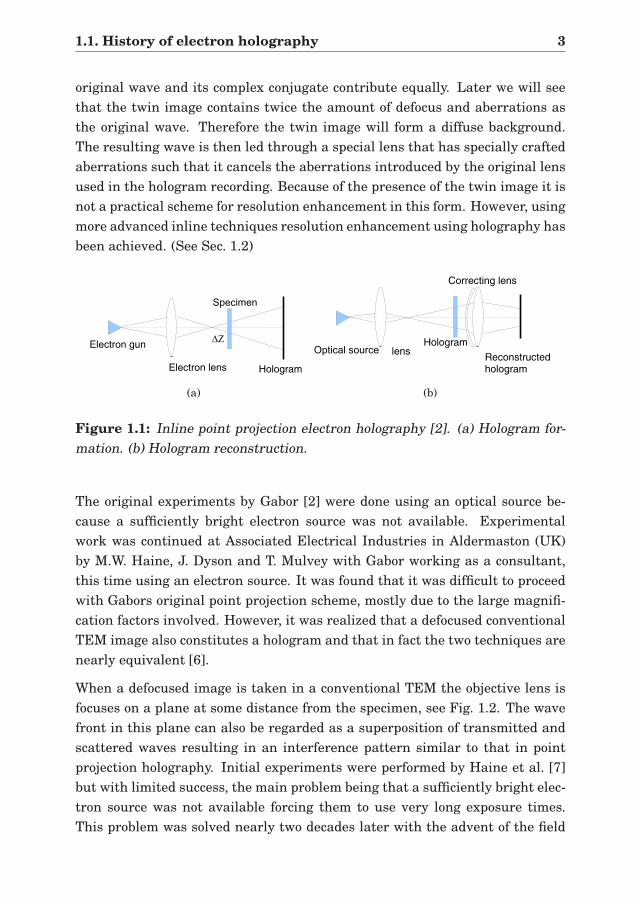
The original holographic setup proposed by Gabor is shown in Fig. 1.1, today
this arrangement is referred to as inline point projection electron holography. A
sample is placed a distance ∆z from the focus point of an electron lens. The rea-
son for this arrangement was to provide a coherent illumination of the object.
If the object is sufficiently thin, a large fraction of the beam will be transmitted
(unscattered) by the sample. These unscattered electrons provide a coherent
background with which electrons that have interacted with the object can in-
terfere.
Thus the electron beam transmitted through the specimen given by ψ(r) =ψr(r)+ψo(r) can be split in two parts a reference beam ψr(r)= Ar(r)eiφr(r) and
an object beam ψo(r)= Ao(r)eiφo(r). The intensity at the recording plane is then
given by
Ihol(r)= |ψ(r)|2 = A2r + A2
o +2Ar Ao cos(φo −φr). (1.1)
It is clear from Eq. (1.1) that both the phase and the amplitude of the object
beam are recorded. If the background is uniform and Ao << Ar then we can
simplify Eq. (1.1)
Ihol(r)≈ 1+2Ao cos(φo −φr), (1.2)
where we have put Ar = 1. The hologram is reconstructed optically by illu-
minating the hologram with a beam that is identical to the original reference
beam.
ψrec(r)= eiφr Ihol = eiφr
[
1+ Aoei(φo−φr) + Aoe−i(φo−φr)]
. (1.3)
The first two terms of Eq. (1.3) together are equal to the original wave. The
third term of Eq. (1.3) is called the twin image and can seriously distort the
resulting image. The twin image arises from the fact that in Eq. (1.1) both the
1.1. History of electron holography 3
original wave and its complex conjugate contribute equally. Later we will see
that the twin image contains twice the amount of defocus and aberrations as
the original wave. Therefore the twin image will form a diffuse background.
The resulting wave is then led through a special lens that has specially crafted
aberrations such that it cancels the aberrations introduced by the original lens
used in the hologram recording. Because of the presence of the twin image it is
not a practical scheme for resolution enhancement in this form. However, using
more advanced inline techniques resolution enhancement using holography has
been achieved. (See Sec. 1.2)
(a) (b)
Figure 1.1: Inline point projection electron holography [2]. (a) Hologram for-
mation. (b) Hologram reconstruction.
The original experiments by Gabor [2] were done using an optical source be-
cause a sufficiently bright electron source was not available. Experimental
work was continued at Associated Electrical Industries in Aldermaston (UK)
by M.W. Haine, J. Dyson and T. Mulvey with Gabor working as a consultant,
this time using an electron source. It was found that it was difficult to proceed
with Gabors original point projection scheme, mostly due to the large magnifi-
cation factors involved. However, it was realized that a defocused conventional
TEM image also constitutes a hologram and that in fact the two techniques are
nearly equivalent [6].
When a defocused image is taken in a conventional TEM the objective lens is
focuses on a plane at some distance from the specimen, see Fig. 1.2. The wave
front in this plane can also be regarded as a superposition of transmitted and
scattered waves resulting in an interference pattern similar to that in point
projection holography. Initial experiments were performed by Haine et al. [7]
but with limited success, the main problem being that a sufficiently bright elec-
tron source was not available forcing them to use very long exposure times.
This problem was solved nearly two decades later with the advent of the field

4 Introduction
emission gun.
Figure 1.2: Inline electron holography [6, 7].
Towards the late 1950’ties interest in the technique faded partly because the
electron microscope at that time had not progressed far enough and partly be-
cause of the twin image problem [4]. However, in the early 1960’ties Leith and
Upatnieks [8] successfully implemented a new scheme using laser light called
off-axis holography. This then led to a major revival of interest in holography
albeit for a very different application then in Gabors original scheme. The main
difference between off-axis and inline holography is that the reference beam is
not transmitted through the specimen but is transmitted along side the spec-
imen as is shown in Fig. 1.3(a). A beam of laser light is split into two parts,
one half will serve as a reference wave which is assumed to be a plane wave
ψr(r) = Ar(r)eik·r. The other half of the beam is used to illuminate the spec-
imen which then serves as object wave ψo(r) = Ao(r)ei(k·r+φo(r)). Both beams
then combine at an angle from each other at the image plane and produce an
interference pattern
I = |ψr +ψo|2 = A2o + A2
r +2A0 Ar cos(2k∥ ·r−φ(r)). (1.4)
Where k∥ is the component of k parallel to the photographic plate, equally we
define k⊥ to be perpendicular to the photographic plate. The resulting hologram
can then be reconstructed by the same setup but now with the object removed,
as is shown in Fig. 1.3(b). This results in a reconstructed wave given by
φr I = Ar eik⊥·r{
(A2o + A2
r )eik∥·r + A0 Ar ei(3k∥·r−φ(r)) + A0 Ar e−i(k∥·r−φ(r))}
. (1.5)
The third term in Eq. (1.5) is just the original object wave modified in am-
plitude. As we assume the reference wave to be uniform this modification in
amplitude will not alter the visual appearance. In this case there is no twin
image problem because the first two terms in Eq. (1.5) are spatially separated
from the third.

1.1. History of electron holography 5
(a) (b)
Figure 1.3: Off-axis holography, (a) Recording, (b) Reconstruction.
(a) (b)
Figure 1.4: (a) Fresnel biprism, (b) Electron biprism.
To implement the off-axis scheme in electron holography an electron interfer-
ometer is needed. The first successful electron interferometer was build by Mar-
ton [9] in the early 1950’ties using multiple single crystal films. Even though
a number of successful experiments were performed (see e.g. Ref. [10]) there
were some practical problems with this design. The interferometer relied on the
alignment of multiple thin films which is difficult to achieve experimentally. An
experimentally much simpler design was made by Möllenstedt en Düker dur-
ing the same period [11]. The design is basically an electron version of Fresnel’s
biprism [12], the electron biprism is now by far the most common electron in-
terferometer. The story behind the development of the electron biprism is told
by Möllenstedt himself in chapter 1 of Ref. [13].
In Fig. 1.4(a) we show Fresnel’s biprism. The biprism effectively splits the orig-
inal wave originating from the point S into two separate beams. These appear

6 Introduction
to originate from the virtual sources S1 and S2. It is then straightforward
to derive an expression for the interference pattern. We put the origin of the
coordinate system at S and the observation plane at y = a. Then the phase
difference between the two waves at a point (x,a) is given by the difference in
path length
∆φ=√
(c− x)2 +a2 −√
(c+ x)2 +a2, (1.6)
where c is the distance between the virtual sources and the true source S.
Doing a series expansion to first order of Eq. (1.6) then gives
∆φ≈ 2cx
c2 +a2, (1.7)
which leads to an evenly spaced interference fringes with a fringe spacing given
by ∆x =π(c2+a2)/(2c). In Fig. 1.4(b) we show a schematic picture of an electron
biprism. The biprism consist of a thin filament carrying a voltage which is
embedded between two grounded metallic plates. In the original experiment by
Düker and Möllenstedt a 2µm metalized quartz filament was used. A general
treatment of the interference pattern generated from the scattering of electrons
by an electron biprism is very complicated [14]. However, a good approximation
for the interference pattern caused by electrons scattered close to the filament
is easily derived. The potential due to the biprism is approximately equal to
that of a screened capacitor of internal radius r and external radius R [11, 15],
where r is equal to the filament radius and R is of the same order of magnitude
as the distance between the filament and the grounded plates.
V (x, y)={
Ub ln(x2 + y2)/(2R2 ln(r/R)) r <√
x2 + y2 < R
0 R <√
x2 + y2, (1.8)
where Ub is the biprism voltage which is assumed to be positive. Using a weak
field approximation and assuming small angles the deflection β of an electron
by the biprism potential is given by
β= e
mev0
∫∞
−∞dy
∂V (x, y)
∂x= 2eUb
mev0R2 ln(r/R)arctan
√
R2 − x2i
xi
, (1.9)
where xi is the x-coordinate of the point where the electron enters the cylin-
drical capacitor potential of Eq. 1.9. If we consider only electrons close to the
filament we have xi ≪ R. Typically xi will be in the order of a few µm and R is
the order of mm. Therefore we can approximate Eq. (1.9)
β≈ eUbπ
mev0R2 ln(r/R)sign(xi), (1.10)

1.2. Inline electron holography 7
thus the magnitude of β is approximately constant close to the filament.
The first off-axis holograms was made by Möllenstedt and Wahl in 1968 [16]
who recorded a hologram of a small tungsten wire. The hologram quality was
greatly increased by Tonomura et. al in 1979 who used a field-emission electron
beam that dramatically increased the number of fringes in a hologram [17].
1.2 Inline electron holography
In many practical cases in transmission electron microscopy we can approxi-
mate the exit wave from the sample by a fully coherent wave. This is valid
provided that the sample is sufficiently thin and that the illumination system
of the microscope is sufficiently well aligned. We can then describe the elec-
tron optics by Abbe’s imaging theory [12], which is shown schematically in
Fig. 1.5. The wave front at the back focal plane is given by T(k)Φ(k) where
Φ(k)=F (ψ(r)) is the Fourier transform of original wave and the transfer func-
tion T(k) of the lens is given by
T(k)= eiχ(k). (1.11)
Experimentally the most important factors in χ(k) are the defocus χd(k) and
the spherical aberration χs(k),
χ(k)≈ χd(k)+χs(k)=π∆zλk2 +πCsλ3k4/2, (1.12)
where λ is the wavelength of the electrons, ∆z is the amount of defocus, and Cs
the spherical aberration constant of the lens. The image intensity at the image
plane is then given by I = |ψ(x)⊗ t(x)|2. The effect of t(x) is that it spreads
out the original wave on the image plane and therefore distorting the original
image.
As was discussed in section 1.1, in ordinary TEM inline holography is achieved
by focusing on a plane just behind the sample, to wit an out of focus image.
The wave front in this plane can be regarded as a superposition of transmitted
and scattered waves, the interference pattern between these waves then con-
stitute the hologram. We assume that the effect of the sample on the incoming
wave is small so that the wave in the image plane is given by ψ(r) = 1− ǫ(r),
where we have taken the incoming wave to be unity. The image intensity then
becomes [13, p.42]
I(r)= |(1−ǫ(r))⊗ t(r)|2 = 1−ǫ(r)⊗ t(r)−ǫ∗(r)⊗ t∗(r)+ . . . (1.13)

8 Introduction
where we ignored second order terms in ǫ(r), furthermore we have used that
1× t(r)=F−1 (δ(k)T(k))=F
−1(
δ(k)eiχ(k))
= 1. (1.14)
To reconstruct Eq. 1.13 we take the Fourier transform
F (I(r))= δ(k)−E(k)T(k)−E∗(−k)T∗(−k)+ . . . (1.15)
and multiply this by T∗(k), which after an inverse Fourier transform gives
I(r)= 1−ǫ(r)−ǫ∗(r)⊗ t∗2(r)+ . . .
=ψ(r)−ǫ∗(r)⊗ t∗2(r)+ . . . ,(1.16)
where t2 =F−1(T∗2(k)). From Eq. (1.16) it is clear that we recover the original
wave function ψ(r) but that also in this case a twin image is present. Moreover
t2 contains twice the amount of defocus and lens aberrations as can be easily
seen from Eq. 1.11. Therefore the twin image forms a diffuse background. Note
also that for this scheme the transfer function T(k) of the objective lens has to
be known.
Figure 1.5: Abbe theory of imaging : The wave front in the back focal plane is
given by the Fourier transform of the incoming wave. Here T(k) is the transfer
function of the electron lens. So that the resulting image intensity I(r) is given
by I(r)= |ψ(r)⊗ t(r)|2
Several methods have been proposed to remove the effect of the twin image. A
method which works particularly well for small nano-particles is Fraunhofer
holography. Conventional holograms are taken in the Fresnel (near-field) re-
gion and can therefore be regarded as a Fresnel diffraction pattern. However,
it was shown by Thompson [18, 19] that if the hologram is recorded in the far-
field of the object then the twin image is essentially removed from reconstructed
image. For a particle of size d the far-field condition is met if the distance z be-
tween the image plane and the sample is [12]
|z|≫ d2/λ, (1.17)

1.3. Off-axis electron holography 9
where λ is the wavelength of the illuminating wave. The first realization of this
scheme using an electron source was done by Tonomura et al. [20] who imaged
10nm gold particles. The experimental arrangement is shown in Fig. 1.6. As an
example we consider the case of 200keV electrons (λ= 2.5×10⁻³ nm), for 10nm
particles the far field condition Eq. 1.17 is then met if |z| ≫ 40µm. This large
value of z means that this method is difficult to apply in an unmodified con-
ventional TEM. It would require extremely large amounts of defocus. However,
positive results have been obtained using far-out-of-focus STEM [21].
(a) (b)
Figure 1.6: Setup for Fraunhofer holography [20], (a) Hologram formation,
sample is illuminated by a near parallel beam of electrons. The diffraction
pattern at a distance z behind the sample is then imaged. Where z is chosen so
that the far-field condition is met. (b) Image reconstruction using laser light.
Another approach to remove the twin image is to use one of the many focus
variation methods. In these methods a (large) number of images at different
focus settings is made. This focus series is then reconstructed using a numerical
algorithm. Most notably the work by Kirkland et al. [22, 23] and that of van
Dyck and Op de Beek with various collaborators [24, 25].
1.3 Off-axis electron holography
In off-axis electron holography, a specimen is chosen such that it does not com-
pletely fill the image plane (for example a small magnetic element or the edge
of an extended film). Thus only part of the electron beam passes through the
specimen. An electrostatic biprism, a thin (< 1µm) metallic wire or quartz fiber
coated with gold or platinum, is used to recombine the specimen beam and the
reference beam so that they interfere and form a hologram. The latter is usually
digitized and digital image-processing techniques can be applied to reconstruct
the image of the magnetic domain structure.
10 Introduction
Figure 1.7: Typical off-axis configuration used in electron holography.
Fig. 1.7 shows a ray diagram of the electron beams in holographic mode. The
reference beam is assumed to be a plane wave
ψr(r)= ei2πq·r. (1.18)
As a result of the interaction the object beam with the sample, the wave emerg-
ing from the object is given by
ψo(r)= Ao(r)eiφo(r), (1.19)
where Ao(r) and φo(r) are the amplitude and phase, respectively. After passing
the biprism, the two beams interfere at the image plane
I(r)= |ψr +ψo|2 = 1+ Ao(r)2 +2Ao(r)cos(2πq ·r−φo(r)), (1.20)
forming the hologram. Clearly, the recorded image I(r) contains information
about both the phase and the amplitude of the object beam. The image can be
reconstructed from the hologram by taking the Fourier transform of Eq. (1.20)
F (I(r))= δ(k)+F (Ao(r)2)+δ(k+q)∗F (Ao(r)eiφo(r))+δ(k−q)∗F (Ao(r)e−iφo(r)), (1.21)
where the Fourier transform F (g(r) is defined by
F (g(r))= 1
(2π)3
∫
g(r)eik·r. (1.22)
The four terms of Eq. (1.21) can be interpreted as follows: The first term is
the contribution of electrons that propagate through the system without being
affected by the sample. The second term yields the intensity, that is, the image
obtained by conventional electron microscopy. The third term is the object wave
centered around k = −q. The last term is the complex conjugate of the object
wave centered around k=q.

1.3. Off-axis electron holography 11
(a) (b)
(c) (d)
Figure 1.8: Step-by-step procedure to reconstruct the phase from an electron
hologram of nanocrystaline Fe94N5Zr1 [26]. (a): hologram; (b): power spectrum
with two side bands; (c): one side band becomes centered; (d): inverse Fourier
transform and phase map φo(x, y) = arctan(I /R) where R and I are the real
and imaginary part of the inverse FFT, respectively.
The phase and amplitude can be numerical reconstructed following the fol-
lowing procedure, illustrated in Fig. 1.8. First the fast Fourier transforma-
tion (FFT) of the holographic image is taken. In frequency domain two side-
bands can be detected. If one of the two side bands of the FFT is cut out
and centered and the inverse FFT of this centered sideband is taken the phase
and amplitude can be calculated using the formulas: φo(r) = arctan(I /R) and

12 Introduction
Ao(r) = (R2 +I2)1/2, where R and I are the real and imaginary part of the
inverse Fourier transform, respectively [27].
The final result of the procedure, sketched above, is a image of the amplitude
Ao(r) and phase φo(r). Evidently, the main question is how these images relate
to the electrical and/or magnetic properties of the sample. If neither the mag-
netic flux B or the crystal potential V vary with depth and neglecting magnetic
and electric fields outside the sample, the phase φ(x, y) in the image plane is
given by an electric contribution φe(x, y) and a magnetic contribution φm(x, y).
However, in reality this relation is more complicated and it is the main theme
of this thesis to unravel the relation between the magnetic/electric structure in
the material and the electron hologram that is being observed.
1.4 Electron interference
As explained earlier, electron holography exploits the wave-like character of
the electron beam. On the other hand, an electron beam consists of individual
electrons. This raises the question of what happens if we consider the situation
in which the intensity of the electron beam is reduced up to the point that at
any time there is only one electron traveling from the source to the detector.
This situation is not at all imaginary because, as we discuss in this section,
such experiments have been carried out and touch one of the most intricate
aspects of our current picture of the microscopic world.
The double slit experiment with electrons is no doubt one of the most funda-
mental experiments in physics. In his lectures on physics Richard Feynman
used the double slit experiment to introduce the subject of quantum mechanics.
He motivated this choice as follows [28] :
We choose to examine a phenomenon which is impossible, abso-
lutely impossible, to explain in any classical way, and which has in
it the heart of quantum mechanics. In reality, it contains the only
mystery.
In Fig. 1.9 a schematic picture is given of the arrangement considered by Feyn-
man. A beam of electrons is emitted from a source towards an aperture con-
taining two slits A and B. If only one of the slits is open then an intensity
distribution forms which has its maximum directly behind the slit and then de-
clines as you move away from it. However, when both slits are open instead of a

1.4. Electron interference 13
superposition of two of these distributions an interference pattern arises. Thus
in this experiment wave-like interference between the electrons are found even
though electrons are observed as particles.
In his lecture Feynman warns that in reality this experiment cannot be per-
formed in this form because of the small dimensions of the experimental ar-
rangement. However, already in 1961 essentially this experiment was per-
formed by Claus Jönsson [29] in Tübingen. In this experiment copper aper-
tures were created containing up to five slits, each slit having a width of 0.3µm
and a spacing of 1µm. Interference patterns were then observed using a 50 kV
electron beam, in good agreement with theory.
Figure 1.9: Double slit experiment
with electrons. I(II) The intensity
distribution when only slit A(B) is
open. III The intensity distribution
with both slits open.
Figure 1.10: Electron biprism,
the electro static potential of the
biprism divides the wave front at
both sides of the filament resulting
in an interference pattern.
The double slit experiment is also achieved with an electron biprism [11] which
is described in detail in section 1. Schematically this situation is shown in
Fig. 1.10.A simple explanation for the interference pattern in the double slit
experiment could be that it is due to some direct interaction between electrons
after they diffract from the grating. However, in 1987 Tonomura et al. [30]
performed a biprism interference experiment where with extremely high prob-
ability only one electron is present in the column at any given time. Moreover
the build-up of the interference pattern is recorded event by event.
In Fig. 1.11 the buildup of the interference pattern at different stages is shown.
It is clear that only after a large amount of events have been recorded a clear
interference pattern emerges. In Fig. 1.12 an intensity profile of Fig. 1.11(d) is
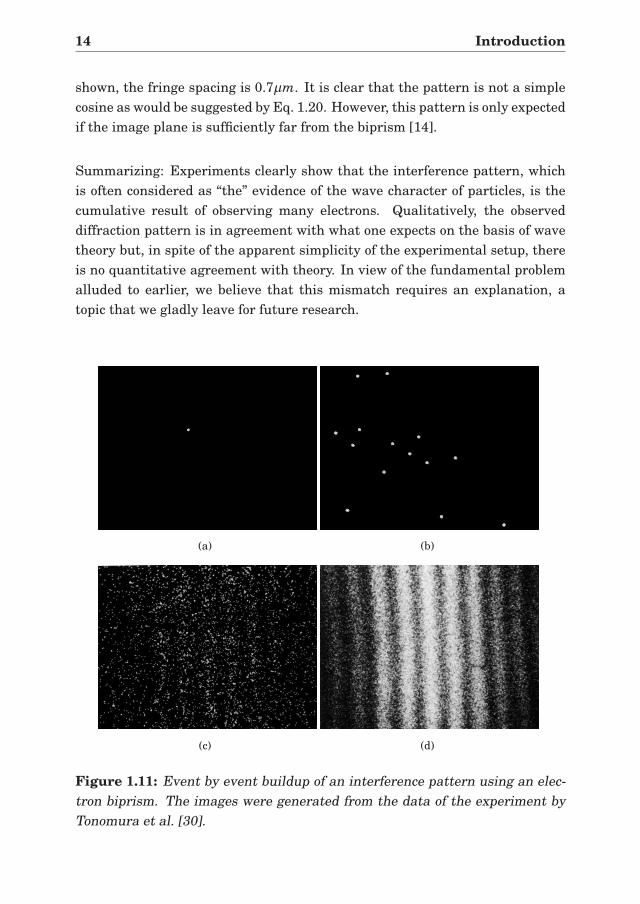
14 Introduction
shown, the fringe spacing is 0.7µm. It is clear that the pattern is not a simple
cosine as would be suggested by Eq. 1.20. However, this pattern is only expected
if the image plane is sufficiently far from the biprism [14].
Summarizing: Experiments clearly show that the interference pattern, which
is often considered as “the” evidence of the wave character of particles, is the
cumulative result of observing many electrons. Qualitatively, the observed
diffraction pattern is in agreement with what one expects on the basis of wave
theory but, in spite of the apparent simplicity of the experimental setup, there
is no quantitative agreement with theory. In view of the fundamental problem
alluded to earlier, we believe that this mismatch requires an explanation, a
topic that we gladly leave for future research.
(a) (b)
(c) (d)
Figure 1.11: Event by event buildup of an interference pattern using an elec-
tron biprism. The images were generated from the data of the experiment by
Tonomura et al. [30].

1.4. Electron interference 15
−3 −2 −1 0 1 2 30
50
100
150
200
250
µm
Inte
nsity
Figure 1.12: Intensity profile of the interference pattern of Fig. 1.11(d)

16 Introduction
Top Related