


Languages
Pages
Legal

Carnegie Mellon UniversityResearch Showcase @ CMU
Computer Science Department School of Computer Science
1984
The design of an LSI Booth multiplier : nMOS vs.CMOS technologyMarco AnnaratoneCarnegie Mellon University
Wen-Zen Shen
Follow this and additional works at: http://repository.cmu.edu/compsci
This Technical Report is brought to you for free and open access by the School of Computer Science at Research Showcase @ CMU. It has beenaccepted for inclusion in Computer Science Department by an authorized administrator of Research Showcase @ CMU. For more information, pleasecontact [email protected].

NOTICE WARNING CONCERNING COPYRIGHT RESTRICTIONS: The copyright law of the United States (title 17, U.S. Code) governs the making of photocopies or other reproductions of copyrighted material. Any copying of this document without permission of its author may be prohibited by law.
C M U - C S - 8 4 - 1 5 0
C 9- in
The Design of an LSI Booth Multiplier:
nMOS vs. CMOS Technology
Marco Annaratone Department of Computer Science
Carnegie-Mellon University Pittsburgh, PA 15232
U.S.A.
Wen-Zen Shen Institute of Electronics'
National Chiao-Tung University Hsin-Chiu, Taiwan Republic of China
Copyright 1984 Marco Annaratone and Wen-Zen Shen
The research was supported in part by the Defense Advanced Research Projects Agency (DoD), ARPA Order No. 3597, monitored by the Air Force Avionics Laboratory under Contract F33615-81-K-1539.
University Libraries Carnegie Mellon University P i t t s b u r g h PA 15213-389Ó
TABLE OF CONTENTS
Table of Contents 1 . Introduction 2 . The Design of a Multiplier Based on the Modified Booth Algorithm
2.1. Basic Building-blocks Inside the Array 2.2. The Problem of Sign Extension
3. The Implementat ion of a 16-bi t nMOS Booth Multipl ier 4. The Implementat ion of a 24-b i t CMOS Booth Multipl ier Appendix A. Layout of some basic cells

LIST OF FIGURES

LIST OF FIGURES III
List of Figures Figure 2-1: The three basic cells that are necessary inside the array of a Booth multiplier 10 Figure 2-2: 8-bit multiplication with the necessary sign extension of the partial products to 10
preserve the correctness of die final result Figure 2-3: Three bits are necessary to handle the sign extension throughout the array 11 Figure 2-4: Block scheme of the module implementing the recoding algorithm 12 Figure 2-5: A straightforward implementation of an 8-bit Boodi multiplier according to the 13
"sign propagate" method Figure 2-6: A more compact scheme for an 8-bit Booth multiplier according to the "sign 14
propagate" method Figure 2-7: Example of the "sign generate" method 16 Figure 2-8: An 8-bit Booth multiplier using the "sign generate" method 17 Figure 3-1: The full-adder scheme 19 Figure 3-2: The full-adder circuit 20 Figure 3-3: Decode logic scheme 20 Figure 3-4: Scheme of the recoding logic (C3) 21 Figure 3-5: Prechargcd full-adder scheme 22 Figure 4-1: CMOS full-adder: logic scheme 24 Figure 4-2: CMOS full-adder: implementation with domino gates 24 Figure 4-3: The dynamic implementation of the selection logic 25 Figure A-l: The floorplan of the nMOS implementation: the floorplan 27
for the CMOS version is conceptually identical Figure A-2: The layout of die nMOS full-adder (top) and decode logic 28 Figure A-3: The layout of the nMOS C3 logic 29 Figure A-4: The layout of the CMOS full-adder and selection logic 30 Figure A-5: The layout of the CMOS C3 logic 31

IV LIST OF TABLES

LIST OF TABLES V
List of Tables Table 2-1: How each rccoded digit influences the A operand 6 Table 2-2: The complete multiplication process 7 Table 2-3: The relationship between partial product and recoded signed digits 8 Table 2-4: Truth table for partial products 8 Table 2-5: Comparison between the two different methods 18

1
Abstract
Although the literature on hardware multipliers is so extensive and the topic is so old, there is no
comprehensive analysis of the Booth algorithm. By comprehensive, we mean a treatment that starts from
the algorithm and goes down to the actual implementation. This paper is mainly focused on the
implementation issues that the Booth algorithm arises. A brief description of the algorithm is also
included.
The usual version of the algorithm will be presented together with a slightly modified
implementation. This different implementation can be considered an improvement over the version
which is usually referred to in the literature: it actually allows to implement the multiplier with less area
without paying a penalty in speed.
This second version has been implemented both in nMOS and CMOS. The two designs are
somewhat opposite in their style and it may be interesting to compare them, especially now that CMOS
has definitely become "the" technology of the eighties. The results of the fabricated and tested nMOS
implementation are presented.

INTRODUCTION
INTRODUCTION 3
1 . Introduction The design of a hardware multiplier obviously depends on the constraints that must be satisfied at
the architectural level, i.e. whether high throughput rather than short latency is desired. In this paper,
latency and area-occupation have been considered the most important figures of merit to be minimized.
Therefore, serial-parallel and strictly serial multipliers will not be dealt with, because of their high
latency. Among all-parallel schemes, the array multiplier has been preferred for its extremely high
regularity.
However, the basic array multiplier, like a Baugh and Wooley scheme for two's complement
multiplication [1] becomes too much area-consuming when it has to process operands with more than 16
bits. This does not mean that it is presently impossible to implement a 32-bit array multiplier in a single
chip. It simply means that the multiplier will occupy most of the available area: therefore, additional
circuitry will have to be placed on different chips with the result of slowing down the execution time
because of off-chip communication.
If we consider the nMOS technology, which is less area-consuming than a corresponding (i.e.
same minimum feature size, same number of interconnection layers) CMOS Bulk technology, a well
laid-out static dill-adder will occupy about 14,000 sq. micron (4/x nMOS). A 32-bit array multiplier
implemented with static nMOS logic would occupy about 14 sq. mm.. Not only is this area too large but,
moreover, problems of power consumption make it a "paper design". If dynamic logic, instead of static
logic, were used, the area occupied by the multiplier would eventually increase (but this is not true for
CMOS, as we shall see later on). Yield is another important consideration that calls for a smaller
circuitry.
Therefore, what we need is a scheme which is not simply faster but also less area-consuming than
that provided by a straightforward array multiplier. If we considered speed as the only parameter, there
would be several schemes that could be used: Wallace trees and Dadda parallel counters are among the
most well-known. On the otbsr hand, it is also well-known that, due to their tree structure, they are not
suitable for a regular implementation. This is not true if we allow a massive pipelining: in [4] it is shown
how a Dadda scheme is indeed regular, when heavily pipelined.
As previously stated, we cannot afford a massive pipelining because of its negative effects on the
latency. Moreover, the multiplier we are interested in is a multiplier that can efficiently process
operands with up to 64 bits each 1 and therefore we cannot use more exotic approaches (e.g. [7], [8]) that
^roughout the entire paper, the expression "n-bit multiplier" will refer to a multiplier that processes two n-bit input operands.

4 INTRODUCTION
usually outperform more common schemes when operands with more than 64-128 bits are concerned.
Another important assumption is that the number system has been considered as given: a
positional number system with radix r = 2, i.e. the usual binary system is assumed; more precisely, two's
complement has been adopted. Interesting results could be achieved by using different number systems
(e.g. the residue number system) but the paper will not address this issue. Nonetheless, a multiplier
featuring regularity and short execution time, still preserving the area-consumption at acceptable levels,
will be interesting also when non-positional number systems are concerned.
The algorithm that has been chosen is die "modified Booth algorithm". Two differenLversions of
the algorithm will be discussed: die former is the usual version that has been adopted in other designs
[9]. The latter handles the sign extension in a more efficient way and leads to a multiplier which is
smaller than the one implemented via the first method.
Two designs \vill be presented and analyzed in detail: a 16-bit nMOS Booth multiplier and a
24-bit CMOS Bulk P-well Booth multiplier. Both of them use the second version of the algorithm.
From an implementation point of view, the two designs are significantly different, since the nMOS-
version is fully static while the CMOS version is fully dynamic. The nMOS version has been fabricated
and tested. Experimental results will be presented.
THE DESIGN OF A MULTIPLIER BASED ON THE MODIFIED BOOTH ALGORITHM 5
2. The Design of a Multiplier Based on the Modified Booth Algorithm The original Booth algorithm [2] did not deal with parallel multiplication but was aimed to
improve the speed of the add-and-shift algorithm.
The Booth algorithm belongs to the class of "recoding" algorithms, i.e. algoridims that "recode"
one of the two operands in such a way that the number of partial products tc be added together
decreases. A simple recoding scheme would consist, for instance, in sequentially considering all the bits
of one operand and in skipping all its zeroes, because they do not contribute to the final result
However, this leads to a variable execution time of the multiplication: if this can still be interesting in
self-timed systems, where a "done" signal can announce the completion of the operation, it is useless in
other timing strategies where the user has to trigger the system on the worst case, i.e. when the operand
has all ones. Actually, the original Booth algorithm itself was not constant in time, although much more
effective than the simple "skipping over Os", because it dealt with strings of Os and Is properly recoded.
A slightly different algorithm, called "modified Booth algorithm" stricdy considers groups of bits
of one operand, rather than being able to skip over arbitrarily long strings. This leads to a longer, but
constant, execution time. The original Booth algorithm is presented in [5] together with its modified
version. A brief analysis of the algoridim will be now introduced for sake of completeness. As an
example, an 8-bit multiplier that multiplies two operands, A = ^ aQ and B = b ? , b Q , will be
considered.
The process of multiplication of two n-bit binary numbers is equivalent, by using a "paper and
pencil" method, to the addition of n, n-bit numbers, properly shifted. This method is used in the array
multipliers. The recoding scheme for the Booth algorithm is presented in [5], Table 3.3, p. 163, for a
bit-pair recoding.
The Booth algorithm decreases the number of rows that have to be added together, therefore
speeding up the computation. The speed up depends on the number of bits that the algorithm considers
in each step. If a bit-pair is considered in each step, the scheme will be called "bit-pair recoding"; the
speed up, if compared to a straightforward implementation via an array multiplier, also depends on how
the two multipliers are implemented. If both of them use a carry-lookahed adder in the last row, the
Booth multiplier will give a speed-up of 40%. Moreover, the area will significantly decrease (again, for a
factor of 40%, roughly). i .
The scheme presented in this paper is the bit-pair recoding. Later on, more complex schemes will
6 THE DESIGN OP A MULTIPLIER BASED ON THE MODIFIED BOOTH ALGORITHM
be considered. The algorithm operates upon one of the two operands and analyzes pairs of bits and
converts them into a set of five signed digit, i.e. 0, + 1 , +2 , -1 and -2. For instance, if the operand B is
(LSB on the right):
0 1 1 0 1 1 1 0
the algorithm, will generate the following recoded string: + 2 -1 0 -2
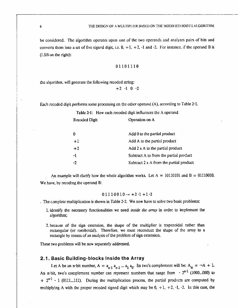
Each recoded digit performs some processing on the other operand (A), according to Table 2-1.
Table 2-1: How each recoded digit influences the A operand
Recoded Digit Operation on A
0 Add 0 to the partial product
+ 1 Add A to the partial product
+ 2 Add 2 x A to the partial product
-1 Subtract A to from the partial product
-2 Subtract 2 x A from the partial product
An example will clarify how die whole algorithm works. Let A = 10110101 and B = 01110010.
We have, by recoding the operand B:
0 1 1 1 0 0 1 0 - > 4-2-1 + 1 - 2
. The complete multiplication is shown in Table 2-2. We now have to solve two basic problems:
1. identify the necessary functionalities we need inside the array in order to implement the algorithm;
2. because of the sign extension, the shape of the multiplier is trapezoidal rather than rectangular (or romboidal). Therefore, we must reconduct the shape of the array to a rectangle by means of an analysis of the problem of sign extension.
These two problems will be now separately addressed.
2 . 1 . Basic Building-blocks Inside the Array Let A be an n-bit number, A = a ^ aQ_2 ... a x aQ. Its two's complement will be: A t e = -»A + 1.
An n-bit, two's complement number can represent numbers that range from - 21 1"1 (1000...000) to
+ 2n~l - 1 (0111...U1). During the multiplication process, the partial products are computed by
multiplying A with the proper recoded signed digit which may be 0, + 1 , +2 , -1 , -2. In this case, the

THE DESIGN OF A MULTIPLIER BASED ON THE MODIFIED BOOTH ALGORITHM 7
A = 1 0 1 1 0 1 0 1
x B = 0 1 1 1 0 0 1 0
0 0 0 0 0 0 0 0 1 0 0 1 0 1 1 0 (-2): take two's complement of A and
1 1 1 1 1 1 1 0 1 1 0 1 0 1
shift left one position
(+l): add A shifted two positions
0 0 0 0 0 1 0 0 1 0 1 1
(note sign extension)
(-1): take two's complement of A
1 1 0 1 1 0 1 0 1 0 (+2): shift left A one position
1 1 0 1 1 1 1 0 1 0 0 1 1 0 1 0 Final 16-bit result
Table 2-2: The complete multiplication process
partial product may range from - 2 n (i.e. + 2 x -211"1) to + 2 n (i.e. -2 x -2n'1). This means that at least
n + 2 bits would be necessary to represent the partial product However, when the two's complement of
a number is taken, there is also an additional "add 1" operation to be performed. Therefore, the
maximum number of bits that are actually needed to represent any partial product is n + 1.
Following the previous discussion, all the partial products can be generated by a structure where
only multiplexing elements and an add operation at the least significant bit is required. Table 2-3 shows
the relationship between the multiplicand A = Xj a 6 ... and a partial product PP = p p g pp 7 ... pp Q .
Apparently, we should perform an extra addition to take into account the add operation on the LSB bi t
However, it is possible to delay this operation by simply using a common carry save technique and a
carry-lookahead adder at the bottom of the array.
As it appears evident from Table 2-3, any partial product can be produced by a multiplexer circuit
and an adder. We have a truth table of the kind shown in Table 2-4, therefore. The boolean equation
that describes the multiplexer is:
PP(j) = xPlAA(i) V xP2AA(i-l) V xMlA-»A(i) V xM2A->A(i-l),
while the logic for the "add 1" block is simply:
add = xMl V xM2.

THE DESIGN OF A MULTIPLIER BASED ON THE MODIFIED BOOTH ALGORITHM
Multiplier Recoded Diqit
Partial Product add Remarks Multiplier Recoded Diqit
PP 8
PP7 P P 6 P P 5 P P 4 P P 3 PP 2 P P 1 p p o
add Remarks
0 0 0 0 0 0 0 0 0 0 0
+1 a 7 3 7 a 6 a 5 a 4 a 3 a 2 a i a o 0
-1 ~7 V 7 T 6 T 5 V 4 ~2 ~ 1 ~ o 1 invert A »nd add 1 to LSB
+2 a 7 3 6 a 5 3 4 a 3 a 2 3 1 a o a - l 0 shift A one position left
-2 ~ 7 ~ 6 ~5 V 4 ~ 3 ~2 ~ 1 ~-l 1 shift A one position left
and add 1 to LSB
Table 2-3: The relationship between partial product and recoded signed digits
Multiplier Recoded Digits
Output add
operation
0 (xO) PP(i) = 0 . for i = 1 00 0
1 (xPl) PP(i) - A(i) for i = 1 0
2 (xP2) PP(i) = A(i-l) for i = 1 00 0
-1 (xMl) PP(i) - A(i) for i = 1 CO 1
-2 (xM2) PP(i) = A(i-l) for i = 1 8 1
Note that A(8) * A(7) » sign bit of multiplicand
PP(8) • sign bit of partial product
Table 2-4: Truth table for partial products

TOE DESIGN OF A MULTIPLIER BASED ON THE MODIFIED BOOTH ALGORITHM 9
The three basic cells we need inside the array to implement a Booth multiplier are shown in Fig.
2-1. A full-adder and two different combinational circuits, called CI and C2 are used. CI is a
multiplexer and C2 is an "add 1" generator.
2.2. The Problem of Sign Extension From the previous discussion, only nine bits and an add operation are necessary to represent any
partial product, being the ninth bit simply used to represent the sign. In order to reduce the array to a
rectangle, the sign extension must be carefully considered. In this section we present two possible
approaches to solve the problem of sign extension. For sake of simplicity, die first approach will be
referred as the "sign propagate" method while the second one will be referred as the "sign generate"
method. The "sign propagate" method has been often used; a CMOS-SOS implementation of it can be
found in [9].
The "Sign Propagate" Method
The partial products in an 8-bit multiplier can be generated by using a 9 x 4 adder array. In order to
achieve a correct result, it is necessary to extend the sign of the partial products (see Fig. 2-2). This
obviously leads to a multiplier that does not have a rectangular shape.
The sign bits of the partial products are located two bits apart from each other. The second partial
product in Fig. 2-2 must propagate to the third row, namely on the sign extension of the third partial
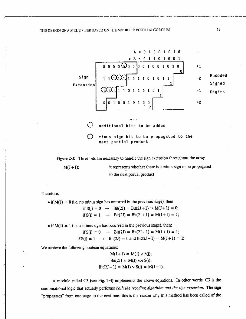
product The problem is graphically shown in Fig. 2-3, where it can be noted that also a third bit is
necessary, in order to propagate a "minus sign" to the next partial product
The sign bit for the j-th partial product PP(j) is defined as: Sö) = xM2(j)AA(7) V xMl(j)AA(7) V xP2(j)AA(7) V xPlAA(7)
We now define four terms:
Bit(2J):
M(J):
Bit(2J+l):
sign extension to be added to the 8th bit of the next
partial product
sign extension to be added to the 9th bit of the next
partial product
it represents whether there is a propagation of a
"minus sign" from the previous partial product

THE DESIGN OF A MULTIPLIER BASED ON THE MODIFIED BOOTH ALGORITHM
PP(i) Cin Sin
A M )
Cout
"7 3 select
Sout
A(-l) = 0 A(-l) = 1
select
1) A(i,-1)
A(i.-l)
CI
PP(i)
T
select
add
Figure 2-1: The three basic cells that are necessary inside the array of a Booth multiplier
A = 0 1 0 0 1 0 1 0
x B = 0 1 1 0 1 0 0 1
Sign Extension
0 0 0 0 0 0 0
1 1 1 1 1
1 1 1
0 0 1 0 0 1 0 1 0
1 0 1 1 0 1 0 1 1
1 1 0 1 1 0 1 0 1
0 1 0 0 1 0 1 0 0
+1
-2
- 1
+2
Recoded Signed
Digits
Figure 2-2: 8-bit multiplication with die necessary sign extension of the partial products to preserve the correctness of the final result
THE DESIGN OF A MULTIPLIER BASED ON THE MODIFIED BOOTH ALGORITHM 11
A = 0 1 0 0 1 B 1 0
x B = 0 1 1 0 1 0 0 1
Sign Extension
0 0 0 0 © 0 0 0 0 1 0 0 1 0 1 L 0 0
1 I Q G X L 1 0 1 1 0 1 0 1 1 1
Q G X D 1 1 0 1 1 0 1 0 1 1
1
0 0 1 0 0 1 0 1 0 0 0
+1
-2
- 1
+2
Recoded Signed
Digits
o additional bits to be added
O minus sign bit to be propagated to the next partial product
Figure 2-3: Three bits are necessary to handle the sign extension throughout the array
M(J+1): *t represents whether there is a minus sign to be propagated
to the next partial product
Therefore:
• if M(J) = 0 (i.e. no minus sign has occurred in the previous stage), then: if S(j) = 0 -> Bit(2J) = B i t ( 2 J + l ) ^ M ( J + l ) = 0; if SQ) = 1 - Bit(2J) = Bit(2J+l) = M ( J + l ) = l;
• if M(J) = 1 (i.e. a minus sign has occurred in the previous stage), then: if S(j) = 0 - Bi t (2J)=Bit (2J+l) = M ( J + l ) = l;
if SQ) = 1 -* Bit(2J) = 0andBitf2J + l ) = M(J+1) = 1;
We achieve the following boolean equations: M(J+1) = M(J)vS(j) ; Bit(2J) = M(J)xorSO);
Bit(2J + l) = M(J) v SO) = M(J+1).
A module called C3 (see Fig. 2-4) implements the above equations. In other words, C3 is the
combinational logic that actually performs both the recoding algorithm and the sign extension. The sign
"propagates" from one stage to the next one: this is the reason why this method has been called of the

12 THE DESIGN OF A MULTIPLIER BASED ON THE MODIFIED BOOTH ALGORITHM
B(2J-l)^
B ( 2 J ) ) B(2J+1)^
C3
M(J+1),
j* y select
(0. +1, +2, - 1 . -2)
^ Bit(2J)
^ Bit(2J+l)
Figure 2-4: Block scheme of the module implementing the recoding algorithm
"sign propagate".
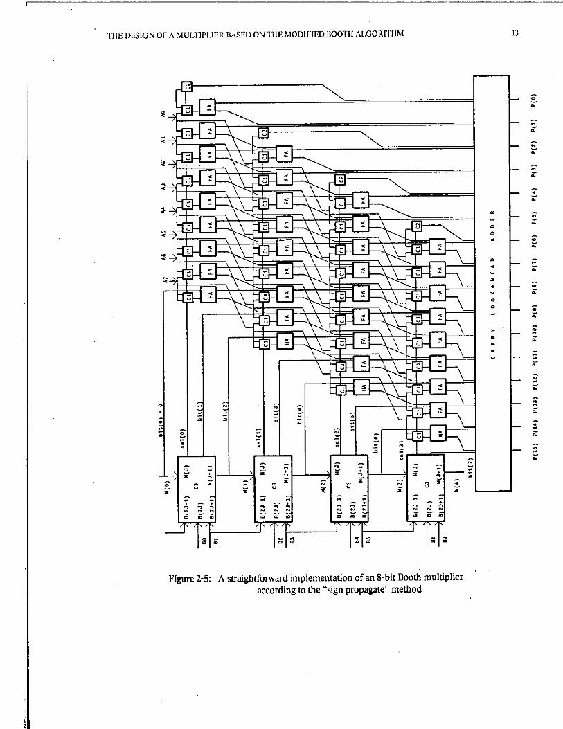
We finally have all the necessary submodules to build the Booth multiplier. Fig. 2-5 shows the
straightforward implementation. The A operand, together with its one's complement (not shown in the
figure) flow across the carry-save adder array. The B operand is simply processed by the C3 blocks tiiat
generate the five selection lines which corresponds to the five signed digits. The Bit(J) terms properly
handle the sign extension. A fast carry lookahed adder is used to furthermore speed up the execution
time.
It is evident from Fig. 2-5 that die delay associated with this scheme is four full-adders plus the
delay introduced by the carry-lookahead adder, provided that the C3 logic be faster than a single-full
adder. It is also evident that the scheme shown in Fig. 2-5 has not been minimized, e.g. the first row has
full-adders with one input only. A much more compact scheme is shown in Fig. 2-6, where only three
rows are used. Moreover, the first one is of half-adders. For an n-bit multiplier, this scheme has
(n/2 -1) rows of (n + 1) fiill-adders (or half-adders) each.
The "Sign Generate" Methpd
A different mediod for sign extension is now presented. The algorithm is discussed for an 8-bit
multiplier, but it can be easily extended to operands with any word-length. We can write the sign bit of
the result as:
S= s ^ ^ + ^ S ^
-MS 3 2? = 8 2 i ) x 2 6 >
г

THE DESIGN OF A MULTIPLIER BASED ON THE MODIFIED BOOTH ALGORITHM
Figure 2-6: A more compact scheme for an 8-bit Booth multiplier according to the "sign propagate" method
THE DESIGN OF A MULTIPLIER BASED ON THE MODIFIED BOOTH ALGORITHM 15
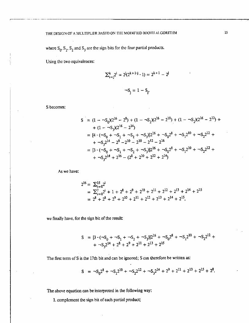
where SQ, S r S 2 and S 3 are the sign bits for the four partial products.
Using the two equivalences:
2 1
k
= j2 i = 2 j ( 2 k + ^ -1) = 2 k + 1 - 2 j
i = 1 " s r
S becomes:
S = (1 - ^SJ(216 - 2 8) + (1 - - S ^ 1 6 - 2 1 0 ) + (1 - - S 2 X 2 1 6 - 2 1 2 ) +
+ (1 - "-S 3)(2 1 6 - 2 1 4 )
= [4 - (^S 0 + ->S1 + -nS2 + -nS 3)]2 1 6 + -nSQ28 + ^ S / 0 + - . S 2 2 1 2 +
+ ^ S 3 2 1 4 - 2 8 - 2 1 0 - 2 1 0 - 2 1 2 - 2 1 6
= [3 - (->S0 + -.Sj + ^ S 2 + -^S 3)]2 1 6 + ->S 02 8 + - ^ S / 0 + - i S 2 2 1 2 +
+ i S 3 2 1 4 + 2 1 6 - (2 8 + 2 1 0 + 2 1 2 + 2 1 4 )
As we have:
2 1 6 = 2^0^ = ^ = o 2 i + l + 2 8 + 2 9 + 2 1 0 + 2 1 1 + 2 1 2 + 2 1 3 + 2 1 4 + 2 1 5
= 2 8 + 2 8 + 2 9 + 2 1 0 + 2 1 1 + 2 n + 2 1 3 + 2 1 4 + 2 1 5 ,
we finally have, for the sign bit of the result:
S = [3 - (- iS 0 + i S 1 + -<S2 + -«S 3)]2 1 6 + - .S Q 2 8 + - - S ^ 1 0 + i S 2 2 1 2 +
+ ^ S 3 2 1 4 + 2 8 + 2 9 + 2 1 1 + 2 1 3 + 2 1 5
The first term of S is the 17th bit and can be ignored; S can therefore be written as:
S = -«S 02 8 + i S ^ 1 0 + ->S22n + ->S 3 2 1 4 + 2 9 + 2 1 1 + 2 1 3 + 2 1 5 + 2 8 .
The above equation can be interpreted in the following way:
1. complement the sign bit of each partial product;

16 THE DESIGN OF A MULTIPLIER BASED ON THE MODIFIED BOOTH ALGORITHM
2. add 1 to the left of the sign bit of each partial product;
3. add 1 to the 9th bit of each partial product
An example is shown in Fig. 2-7. In this approach, that we called "sign generate" method the sign bit
does not really propagate along the left edge of the array muldplier but is, in some sense, "generated"
statically.
1 0 1 1 0 1 0 1
x l O O l l l O l
|*T| means add 1 to the 28-th position
means add 1 to the left of each
partial product
1 1 0 1 1 0 1 0 1
" 0 0 1 0 0 1 0 1 0 © 0 , 1 means complement sign bit 1 0 1 1 0 1 0 1 0
Q o " o i o o i o i o i
Figure 2-7: Example of the "sign generate" method
The hardware of a Booth muldplier that uses this method is different from the one shown in Fig.
2-6. The three operations that are necessary to generate the sign bits involve, as a first step, the negation
of the sign bi t This can be easily accomplished by simply exchanging the A operand with its one's
complement (and viceversa) when they are input to the CI logic.
Fig. 2-8 shows the block scheme of an 8-bit multiplier that uses the "sign generate" method. Note
diat only 8 full-adders are needed for each row. An n-bit multiplier will consist of (n/2 -1) rows with n
full-adders each. Moreover, the C3 logic becomes very simple, because the two terms Bit(2J) and Bit(2J
-f 1) are no longer required. A comparison between the two different methods is shown in Table 2-5.
Finally, some considerations on the choice of a bit-pair receding scheme are worth being made.
Undoubtely, a three-bit recoding scheme seems to be extremely promising, at least for medium-size and
large multipliers (i.e. 24 bit-multipliers and larger). Further significant speed up could be achieved and
the area could be even smaller. There are some good reasons not to implement a three bit-recoding

r
THE DESIGN OF A MULTIPLIER BASED ON THE MODIFIED BOOTH ALGORITHM 17
(*) always zero
Figure 2-8: An 8-bit Booth multiplier using the "sign generate" method

18 THE DESIGN OF A MULTIPLIER BASED ON THE MODIFIED BOOTH ALGORITHM
Table 2-5: Comparison between the two different methods
Sign Propagate Sign Generate
first row with
C3 logic
regularity
array size ( n + l ) x ( n / 2 - l ) n x ( n / 2 - l )
half-adders only (n- l )half-a
Complex Simple
(n -1) half-adders and 1 full-adder
more regular less regular
scheme, though.
In a bit-pah recoding scheme, we need the A and 2 x A terms, together with their one's
complement The 2 x A is a simple shift and die one's complement usually comes for free, provided that
both inverting and non-inverting latches are used at the input of the multiplier. If a three-bit recoding
scheme were used, we would also need the 4 x A term and the 3 x A. The time it takes, especially if long
operands are concerned, to compute the last term definitely discourages the use of more complex
recoding schemes, at least in the VLSI field (arithmetic units inside mainframes have used even four-bit
recoding schemes). One solution, which is usually proposed to overcome these problems, is to compute
the x3 term during idle times, e.g. during precharging. However, this solution does not seem to be easily
applicable:
1. a three-bit recoding scheme does not make sense for small multipliers (up to 16-bit) because the increased complexity is not fairly balanced by significant gains both in area and in speed;
2. as far as larger multipliers are concerned, the time for a, for instance, 32-bit addition (that is what the x3 term consists of) cannot be compared to the precharging time, unless extremely fast adders (i.e. area consuming, not regular etc.) are used.
However, one possibility exists, even in the VLSI field, to use a three-bit recoding scheme, i.e. when the
multiplier is intended to be simply a component of a more complex structure. In this case there might be
a sufficiently long idle time, due to architectural constraints, as to allowing the implementation of a more
complex recoding.
The same observations held, even more strongly, for recoding schemes using more than diree bits.
Only when extremely large multipliers are involved, these schemes can pay off.

THE IMPLEMENTATION OF A 16-liiT NMOS BOOTH MULTIPLIER 19
3. The Implementation of a 16-bit nMOS Booth Multiplier A 16-bit Booth multiplier was first implemented in nMOS with a 3/i minimum feature size. The
use of a purely static logic circuitry was mainly due to the necessity of minimizing die area. For the same
reason, no pipelining was used. In fact, latency, more than throughput, was considered to be the most
important figure of merit, as far as performance are concerned.
The "sign generate" method was implemented. The floorplan of the multiplier is shown in Fig.
A-l (A operand on the right, B operand on the top, resuk on the left and bottom sides). Vdd and GND
run horizontally, together with the A and Abar lines. The five control signals (i.e. xO, xMl, xM2, xPl
and xP2) run vertically in polysilicon. These polysilicon lines have compelled us to use area-consuming
buffers to drive the load (see Fig. A-3). Actually, inverters rather than superbuffers have been used.
This choice, that undoubtely negatively effects the performance, was due to pitch-matching reasons.
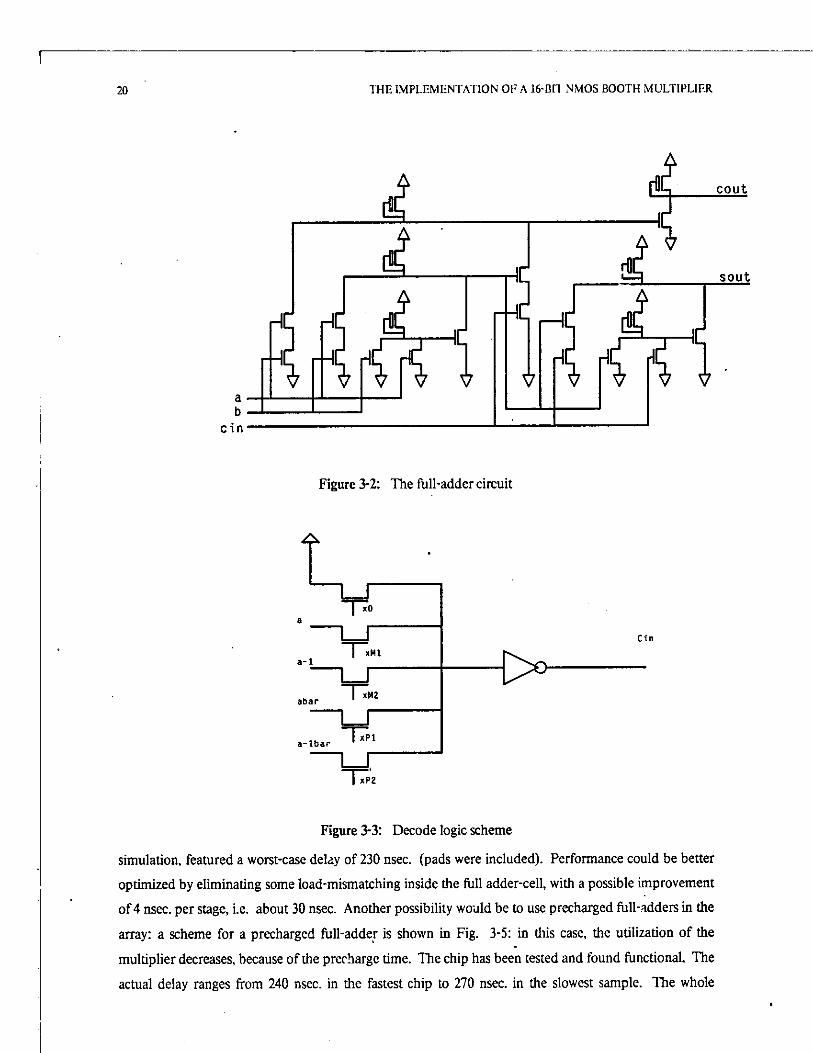
Figure 3-1: The full-adder scheme
The core part of the multiplier is an array of full-adders and multiplexing logic. The left column
contains the recode logic (i.e. the C3 logic). The full-adder scheme, together with its implementation is
shown respectively in Fig. 3-1 and Fig. 3-2. The decode logic is shown in Fig. 3-3. The full-adder and
the decode logic occupy an area of 94.5 x 157.5 /i. The layout of the cell is shown in Fig. A-2. The
scheme of the full-adder is straightforward and does not deserve any comment. The recoding logic was
implemented via a PLA and its scheme is shown in Fig. 3-4. The layout of a single C3 logic circuit is
shown in Fig. A-3. Its area is 303 x 144 /t.
The leftmost column and the bottom row is a 32-bit adder based on the Brent and Kung scheme
[3]. Each half of the 32-bit adder occupies an area of 1405.5 x 349.5 /x. The multiplier, under
20 THE IMPLEMENTATION OF A 16-BH NMOS BOOTH MULTIPLIER
COUt
c i n
Figure 3-2: The full-adder circuit
Cin
Figure 3-3: Decode logic scheme
simulation, featured a worst-case delay of 230 nsec. (pads were included). Performance could be better
optimized by eliminating some load-mismatching inside the full adder-cell, with a possible improvement
of 4 nsec. per stage, i.e. about 30 nsec. Another possibility would be to use precharged full-adders in the
array: a scheme for a precharged full-adder is shown in Fig. 3-5: in tliis case, the utilization of the
multiplier decreases, because of the précharge time. The chip has been tested and found functional. The
actual delay ranges from 240 nsec. in the fastest chip to 270 nsec. in the slowest sample. The whole

THE IMPLEMENTATION OF A 16-BIT NMOS BOOTH MULTIPLIER 21
'i-l
1-1
'1-1 " n > H > o — ^ o —
Figure 3-4: Scheme of the recoding logic (C3)
multiplier occupies an area of 2134.5 x 1599 /i. Careful elimination of load-mismatching and an even
more compact layout might speed up the multiplier to 200 nsec. (data in, data out). No precise data are
available on power consumption; a reasonable figure is about 350 mW.

Figure 3-5: Préchargée! full-adder scheme

THE IMPLEMENTATION OF A 24-BIT CMOS BOOTH MULTIPLIER 23
4. The Implementation of a 24-bit CMOS Booth Multiplier The approach that has been followed in the design of the 24-bit CMOS Booth multiplier was
opposite. CMOS static design is not usually a wise choice, for two main reasons:
1. it is extremely area-consuming (one pull-up device for each pull-down device);
2. it is slow: the capacitance of each input is the contribution of two capacitances, i.e. pull-down's and pull-up's.
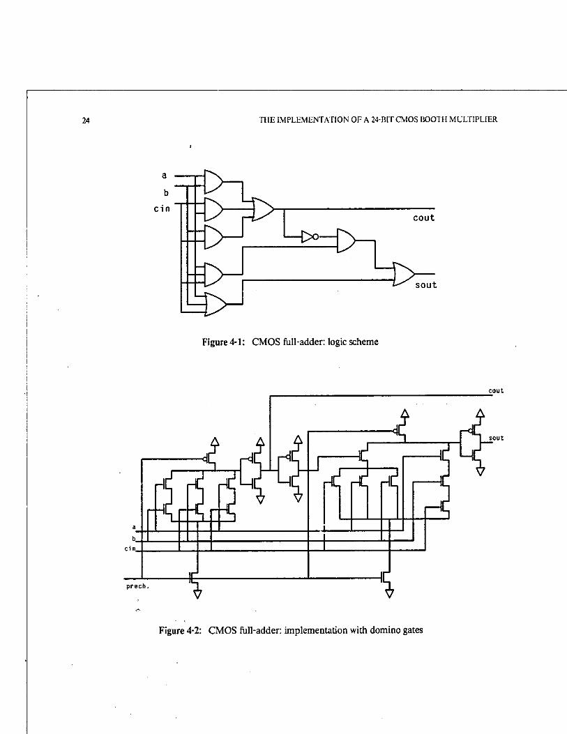
We decided therefore to use some kind of dynamic logic and domino logic [6] has been used. The only
significant drawback of domino logic is that, being a non-inverting logic, an XOR gate is not provided.
This does not significantly affects die design of adders, because carry-lookahead schemes can be almost
completely implemented in domino logic (an XOR is necessary only in the last stage) and actually the
same fast adder used in the nMOS version was used in the CMOS implementation. The major problem
was the design of the full-adder, because of the lack of the XOR gate. The scheme shown in Fig. 4-1 and
Fig. 4-2 features one static inverter only inside the full-adder (besides the buffering inverters used in
domino gates). If the three inputs to the full-adder had been available together widi dieir complements,
different, smaller schemes could have been used. In the case of a multiplier of this kind (and, generally,
with all the array multipliers) it does not seem to. pay off to provide each full-adder with inputs of both
polarities. The layout of the full-adder and selection logic is shown in Fig. A-4.
The CI (selection) logic deserves some comment because it differs from the one used in the
nMOS version. Its scheme is shown in Fig. 4-3. The use of purely static transmission gates was not
considered because it would have been necessary to carry ten selection lines instead of 5. A selection
logic that could use n-channcl transistor only have been chosen. As it is risky to use unilateral
transmission gates in CMOS Bulk, a dynamic logic has been used. The same clock that précharges all
the domino gates in the multiplier, pulls up also the output of the selection logic. Note that, although at
the expense of five more n-channel transistors, there is never a padi from Vdd to GND. When the
précharge signal will go high, the selection logic vill select one of five inputs. At this point, the
n-channel transistors will simply, if the case, pull down the node. As far as the C3 logic is concerned,
after a trivial rearrangement of scheme, a dynamic PLA-like circuit has been designed. Its lay-out is
shown in Fig. A-5. Well and P + masks have been omitted.
The technology used has been CMOS Bulk P-well, with a 3 /i minimum feature size, one level of
metal. The full-adder and selection logic take 131 x 272 /x, while the C3 logic takes 340 x 267 /i. The
24-bit fast adder takes 579 x 3031 /i. The whole multiplier takes 4010 x 3520 /i. The correspondent
24-bit, nMOS multiplier would have taken about 3000 x 2200 ¡1. Even domino logic cannot significantly
THE IMPLEMENTATION OF A 24-BIT CMOS BOOTH MULTIPLIER
Figure 4-1: CMOS fall-adder: logic scheme
cout
Figure 4-2: CMOS full-adder: implementation with domino gates

THE IMPLEMENTATION OF A 24-BIT CMOS BOOTH MULTIPLIER 25
C1n
Figure 4-3: The dynamic implementation of the selection logic
decrease the area consumption, if a comparison with nMOS is made. However, the decrease in area is
significant when we take into account a fully static CMOS implementation: a 24-bit Booth CMOS static
multiplier would take about 5500 x 3400 /i.

LAYOUT OF SOME BASIC ŒLLS

LAYOUT OF SOME BASIC CELLS 27
Appendix A Layout of some basic cells
Figure A-l: The floorplan of die nMOS implementation: the floorplan
for the CMOS version is conceptually identical
plamul plamul piamul plamui piar jl plraul plamull
le-'thadd
faddb fadd fadd fadd fadd fadd
faddb fadd fadd fadd fadd fadd
faddb fadd fadd fadd fadd fadd
faddb fadd fadd fadd fadd fadd
faddb fadd fadd fadd fadd fadd
faddb fadd fadd fadd fadd fadd
faddb fadd fadd fadd fadd fadd
faddb fadd fadd fadd fadd fadd h ddlï L mpxrc
faddb fadd fadd fadd fadd fadd
faddb fadd fadd fadd fadd fadd
faddb fadd fadd fadd fadd fadd
faddb fadd fadd fadd fadd fadd
faddb fadd fadd fadd fadd >
fadd
faddb fadd fadd fadd fadd fadd
faddrb faddr faddr faddr faddr faddr
.Ércol


LAYOUT OF SOME BASIC CELLS
Figure A-3: The layout of the nMOS C3 logie

30 LAYOUT OF SOME BASIC CELLS
Figure A-4: The layout of the CMOS full-adder and selection logic

LAYOUT OF SOME BASIC CELLS
Figure A-5: The layout of the CMOS C3 logie

32 LAYOUT OF SOME BASIC CELLS
References
[1] Baugh, C R . and Wooley, B.A. A Two's Complement Parallel Array Multiplication Algorithm. IEEE Trans, on Comput. C-22:1045-1047,1973.
[2] Booth, A.D. A Signed Binary Multiplication Technique. Q.J. Mech Appl. Math 4:236-240,1951.
[3] Brent, R.P. and Kung, H.T. A Regular Layout for Parallel Adders. IEEE Trans, on Comput., 1981.
[4] Cappello, P.R. and Steiglitz, K. A VLSI Layout for a Pipelined Dadda Multiplier. ACM Trans, on Computer Systems 1(2): 157-174, May, 1983.
[5] Cavanagh, J.J.F. Computer Science Series: Digital Computer Arithmetic. McGraw-Hill Book Co., 1984.
[6] Krambeck, R.H., Lee, C M . and Law, H.S. High-speed Compact Circuits with CMOS. IEEE Journal Solid State Circuits SC-17(3):614-619, June, 1982.
[7] Luk, W.K. A Regular Layout for Parallel Multiplier of 0(log 2n] Time. In Kung, H.T., Sproull, R.F. and Steele, G.L., Jr. (editor), VLSI Systems and Computations,
pages 317-326. Computer-Science Department, Carnegie-Mellon Univeristy, Computer Science Press, Inc., October, 1981.
[8] Preparata, F.P. A Mesh-Connected Area-Time Optimal VLSI Integer Multiplier. In Kung, H.T., Sproull, R.F., and Steele, G.L., Jr. (editors), VLSI Systems and Computations,
pages 311-316. Computer Science Department, Carnegie-Mellon University, Computer Science Press, Inc., October, 1981.
[9] Ware, F.A., McAllister, W.H., Carlson, J.R., Sun, D.K. and Vlach, R.J. 64 Bit Monolithic Floating Point Processors. IEEE Journal of Solid-State C/raWsC-17(5):898-907, October, 1982.
Top Related