


Languages
Pages
Legal

Testing of Logic Circuits
2
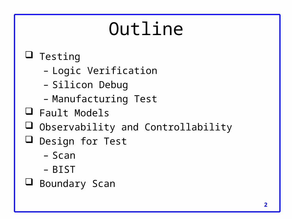
Outline Testing
– Logic Verification– Silicon Debug– Manufacturing Test
Fault Models Observability and Controllability Design for Test
– Scan– BIST
Boundary Scan
3
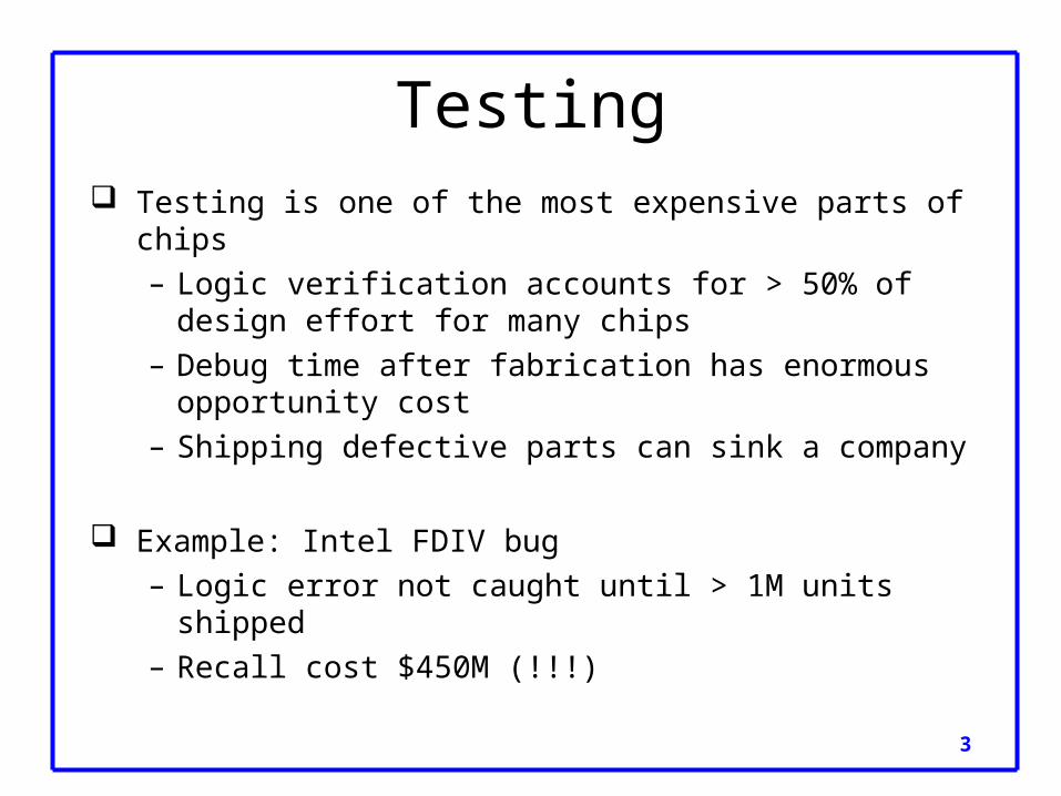
Testing Testing is one of the most expensive parts of chips
– Logic verification accounts for > 50% of design effort for many chips
– Debug time after fabrication has enormous opportunity cost
– Shipping defective parts can sink a company
Example: Intel FDIV bug– Logic error not caught until > 1M units shipped– Recall cost $450M (!!!)
4
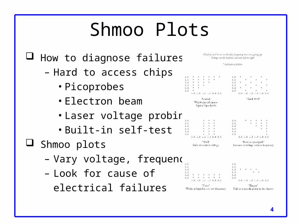
Shmoo Plots How to diagnose failures?
– Hard to access chips• Picoprobes• Electron beam• Laser voltage probing• Built-in self-test
Shmoo plots– Vary voltage, frequency– Look for cause of
electrical failures
5
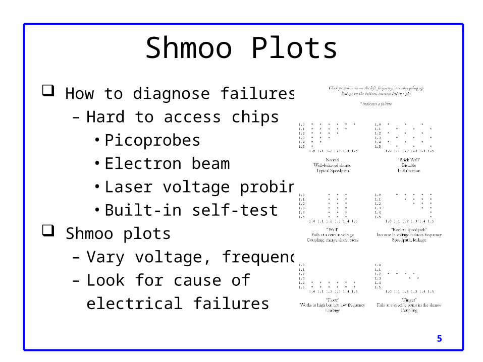
Shmoo Plots How to diagnose failures?
– Hard to access chips• Picoprobes• Electron beam• Laser voltage probing• Built-in self-test
Shmoo plots– Vary voltage, frequency– Look for cause of
electrical failures

6
Manufacturing Test A speck of dust on a wafer is sufficient to kill chip Yield of any chip is < 100%
– Must test chips after manufacturing before delivery to customers to only ship good parts
Manufacturing testers are
very expensive– Minimize time on tester– Careful selection of
test vectors
7
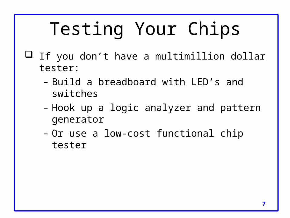
Testing Your Chips If you don’t have a multimillion dollar tester:
– Build a breadboard with LED’s and switches– Hook up a logic analyzer and pattern generator– Or use a low-cost functional chip tester

8
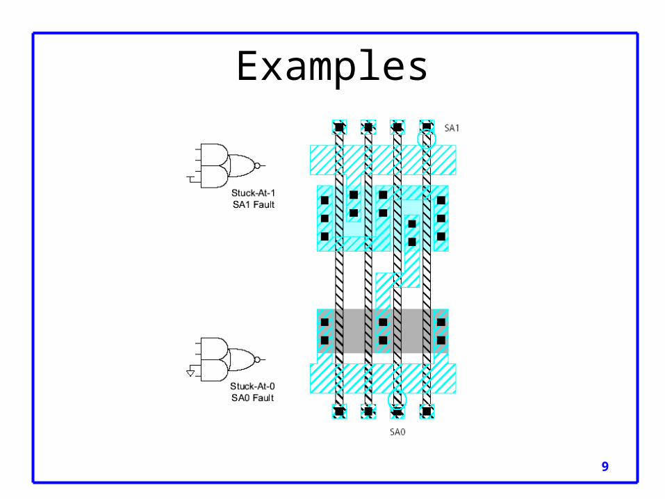
Stuck-At Faults How does a chip fail?
– Usually failures are shorts between two conductors or opens in a conductor
– This can cause very complicated behavior A simpler model: Stuck-At
– Assume all failures cause nodes to be “stuck-at” 0 or 1, i.e. shorted to GND or VDD
– Not quite true, but works well in practice
9
Examples
10
Observability & Controllability
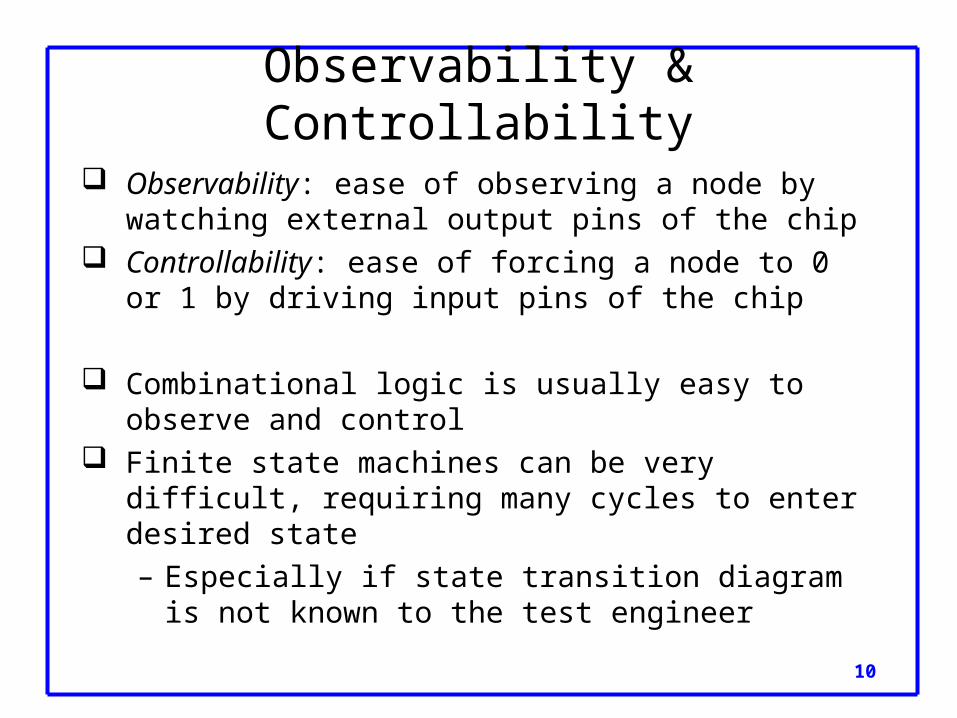
Observability: ease of observing a node by watching external output pins of the chip
Controllability: ease of forcing a node to 0 or 1 by driving input pins of the chip
Combinational logic is usually easy to observe and control
Finite state machines can be very difficult, requiring many cycles to enter desired state– Especially if state transition diagram is not known
to the test engineer

11
Test Pattern Generation Manufacturing test ideally would check every node in
the circuit to prove it is not stuck. Apply the smallest sequence of test vectors
necessary to prove each node is not stuck.
Good observability and controllability reduces number of test vectors required for manufacturing test.– Reduces the cost of testing– Motivates design-for-test

12
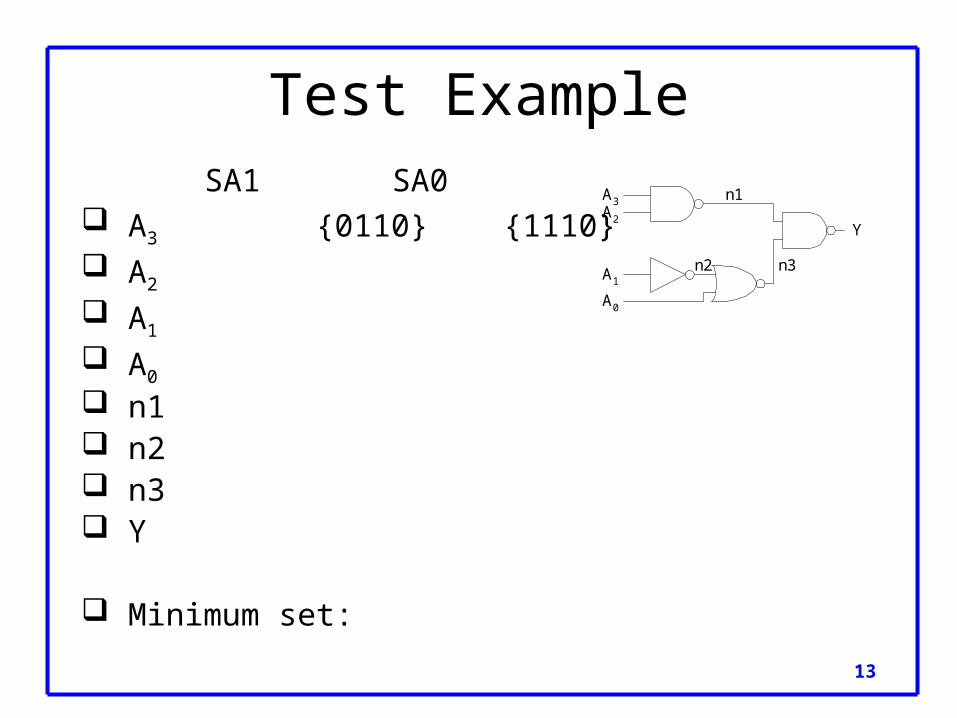
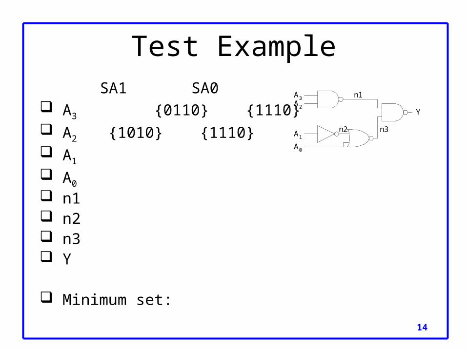
Test ExampleSA1 SA0
A3 A2
A1
A0
n1 n2 n3 Y
Minimum set:
A3A2
A1
A0
Y
n1
n2 n3
13
Test ExampleSA1 SA0
A3 {0110} {1110} A2
A1
A0
n1 n2 n3 Y
Minimum set:
A3A2
A1
A0
Y
n1
n2 n3
14
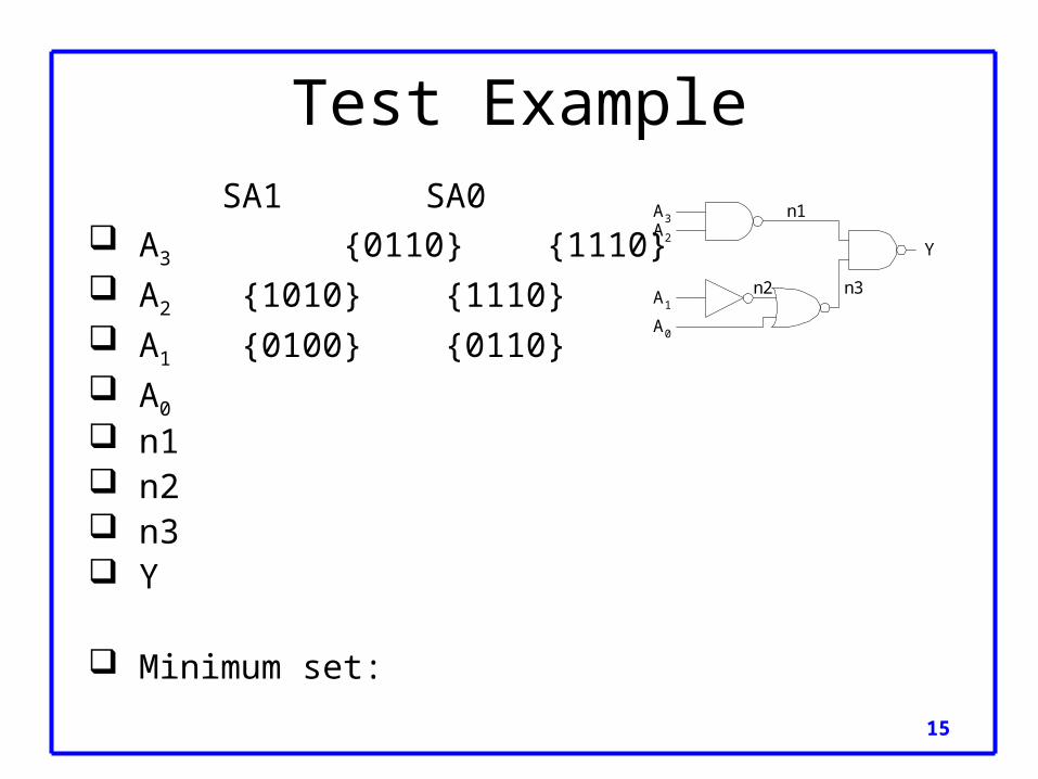
Test ExampleSA1 SA0
A3 {0110} {1110} A2 {1010} {1110} A1
A0
n1 n2 n3 Y
Minimum set:
A3A2
A1
A0
Y
n1
n2 n3
15
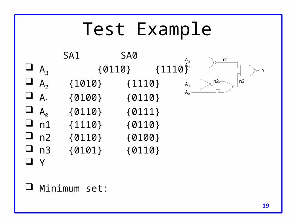
Test ExampleSA1 SA0
A3 {0110} {1110} A2 {1010} {1110} A1 {0100} {0110} A0
n1 n2 n3 Y
Minimum set:
A3A2
A1
A0
Y
n1
n2 n3
16
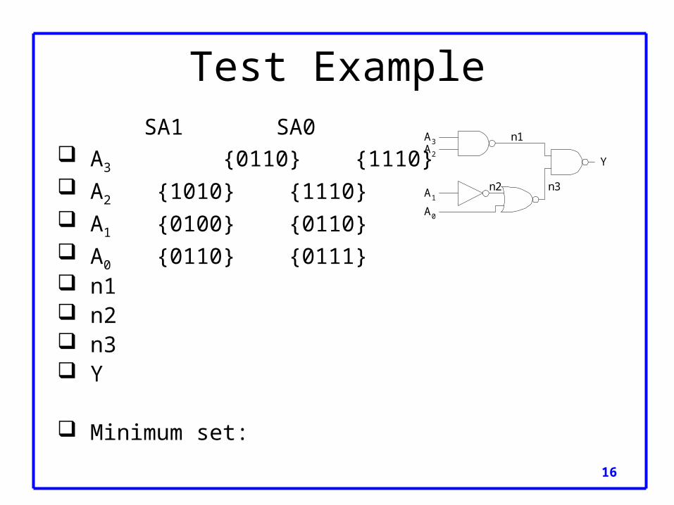
Test ExampleSA1 SA0
A3 {0110} {1110} A2 {1010} {1110} A1 {0100} {0110} A0 {0110} {0111} n1 n2 n3 Y
Minimum set:
A3A2
A1
A0
Y
n1
n2 n3

17
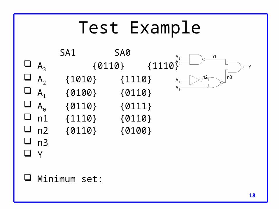
Test ExampleSA1 SA0
A3 {0110} {1110} A2 {1010} {1110} A1 {0100} {0110} A0 {0110} {0111} n1 {1110} {0110} n2 n3 Y
Minimum set:
A3A2
A1
A0
Y
n1
n2 n3
18
Test ExampleSA1 SA0
A3 {0110} {1110} A2 {1010} {1110} A1 {0100} {0110} A0 {0110} {0111} n1 {1110} {0110} n2 {0110} {0100} n3 Y
Minimum set:
A3A2
A1
A0
Y
n1
n2 n3
19
Test ExampleSA1 SA0
A3 {0110} {1110} A2 {1010} {1110} A1 {0100} {0110} A0 {0110} {0111} n1 {1110} {0110} n2 {0110} {0100} n3 {0101} {0110} Y
Minimum set:
A3A2
A1
A0
Y
n1
n2 n3
20
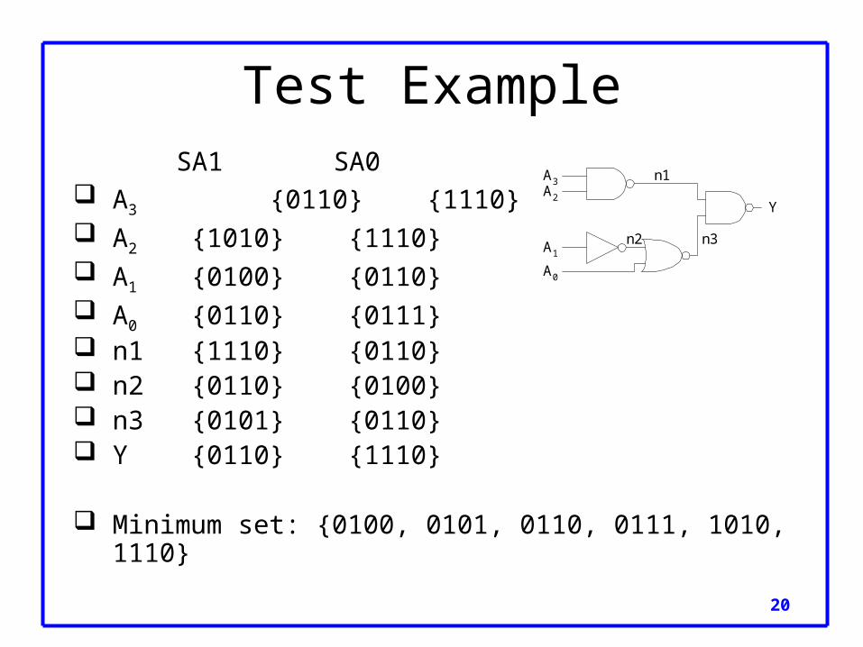
Test ExampleSA1 SA0
A3 {0110} {1110} A2 {1010} {1110} A1 {0100} {0110} A0 {0110} {0111} n1 {1110} {0110} n2 {0110} {0100} n3 {0101} {0110} Y {0110} {1110}
Minimum set: {0100, 0101, 0110, 0111, 1010, 1110}
A3A2
A1
A0
Y
n1
n2 n3
21
Design for Test Design the chip to increase observability and
controllability
If each register could be observed and controlled, test problem reduces to testing combinational logic between registers.
Better yet, logic blocks could enter test mode where they generate test patterns and report the results automatically.
22
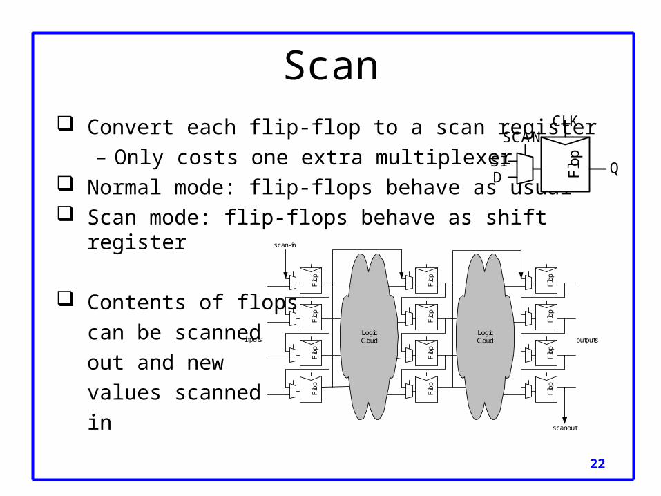
Scan Convert each flip-flop to a scan register
– Only costs one extra multiplexer Normal mode: flip-flops behave as usual Scan mode: flip-flops behave as shift register
Contents of flops
can be scanned
out and new
values scanned
in
Flo
p
QD
CLK
SI
SCAN
scan out
scan-in
inputs outputs
Flo
pF
lop
Flo
pF
lop
Flo
pF
lop
Flo
pF
lop
Flo
pF
lop
Flo
pF
lop
LogicCloud
LogicCloud
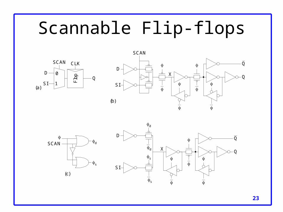
23
Scannable Flip-flops
0
1 Flo
p
CLK
D
SI
SCAN
Q
D
X
Q
Q
(a)
(b)
SCAN
SI
D
X
Q
Q
SI
s
s
(c)
d
d
d
s
SCAN
24
Built-in Self-test Built-in self-test lets blocks test themselves
– Generate pseudo-random inputs to comb. logic– Combine outputs into a syndrome– With high probability, block is fault-free if it
produces the expected syndrome

25
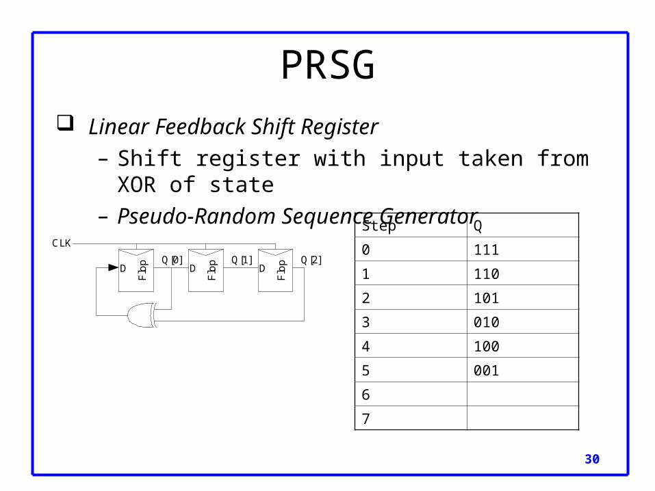
PRSG Linear Feedback Shift Register
– Shift register with input taken from XOR of state– Pseudo-Random Sequence Generator
Flo
p
Flo
p
Flo
pQ[0] Q[1] Q[2]
CLK
D D D
Step Q
0 111
1
2
3
4
5
6
7

26
PRSG Linear Feedback Shift Register
– Shift register with input taken from XOR of state– Pseudo-Random Sequence Generator
Flo
p
Flo
p
Flo
pQ[0] Q[1] Q[2]
CLK
D D D
Step Q
0 111
1 110
2
3
4
5
6
7

27
PRSG Linear Feedback Shift Register
– Shift register with input taken from XOR of state– Pseudo-Random Sequence Generator
Flo
p
Flo
p
Flo
pQ[0] Q[1] Q[2]
CLK
D D D
Step Q
0 111
1 110
2 101
3
4
5
6
7
28
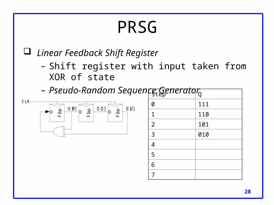
PRSG Linear Feedback Shift Register
– Shift register with input taken from XOR of state– Pseudo-Random Sequence Generator
Flo
p
Flo
p
Flo
pQ[0] Q[1] Q[2]
CLK
D D D
Step Q
0 111
1 110
2 101
3 010
4
5
6
7
29
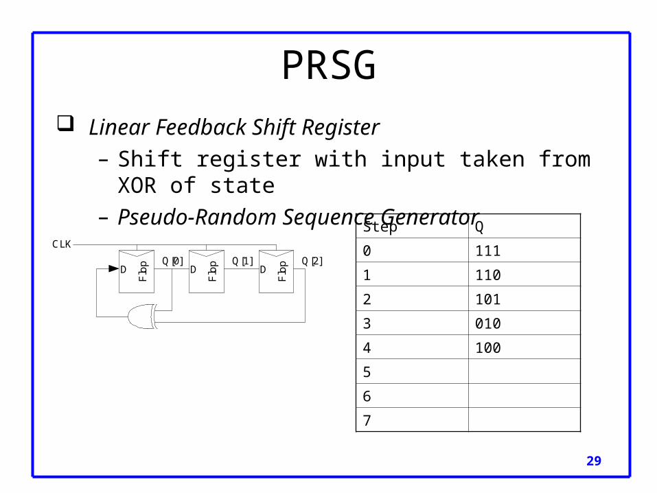
PRSG Linear Feedback Shift Register
– Shift register with input taken from XOR of state– Pseudo-Random Sequence Generator
Flo
p
Flo
p
Flo
pQ[0] Q[1] Q[2]
CLK
D D D
Step Q
0 111
1 110
2 101
3 010
4 100
5
6
7
30
PRSG Linear Feedback Shift Register
– Shift register with input taken from XOR of state– Pseudo-Random Sequence Generator
Flo
p
Flo
p
Flo
pQ[0] Q[1] Q[2]
CLK
D D D
Step Q
0 111
1 110
2 101
3 010
4 100
5 001
6
7
31
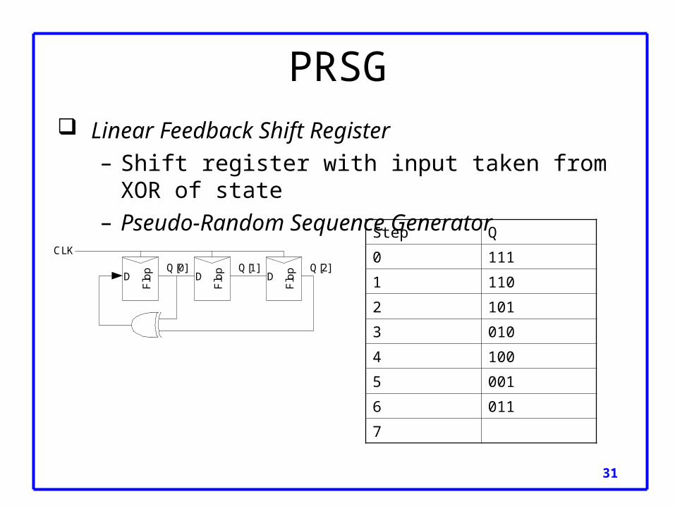
PRSG Linear Feedback Shift Register
– Shift register with input taken from XOR of state– Pseudo-Random Sequence Generator
Flo
p
Flo
p
Flo
pQ[0] Q[1] Q[2]
CLK
D D D
Step Q
0 111
1 110
2 101
3 010
4 100
5 001
6 011
7

32
PRSG Linear Feedback Shift Register
– Shift register with input taken from XOR of state– Pseudo-Random Sequence Generator
Flo
p
Flo
p
Flo
pQ[0] Q[1] Q[2]
CLK
D D D
Step Q
0 111
1 110
2 101
3 010
4 100
5 001
6 011
7 111 (repeats)
33
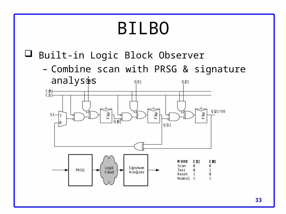
BILBO Built-in Logic Block Observer
– Combine scan with PRSG & signature analysis
MODE C[1] C[0]Scan 0 0Test 0 1Reset 1 0Normal 1 1
Flo
p
Flo
p
Flo
p
1
0
D[0] D[1] D[2]
Q[0]Q[1]
Q[2] / SOSI
C[1]C[0]
PRSGLogicCloud
SignatureAnalyzer
34
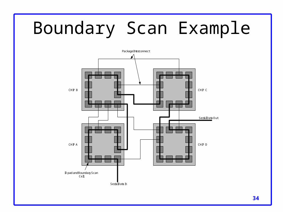
Boundary Scan Example
Serial Data In
Serial Data Out
Package Interconnect
IO pad and Boundary ScanCell
CHIP A
CHIP B CHIP C
CHIP D

35
Summary Think about testing from the beginning
– Simulate as you go– Plan for test after fabrication
“If you don’t test it, it won’t work! (Guaranteed)”
Top Related