


Languages
Pages
Legal


C2S2 Workshop1
SRAM design challengesSRAM design challengesin nanoin nano--scale CMOS scale CMOS
Vivek DeVivek DeCircuits Research LabCircuits Research Lab
Acknowledgment:M. Agostinelli, A. Farhang, F. Hamzaoglu, A. Keshavarzi,
D. Khalil, M. Khellah, N-S. Kim, G. Pandya, S. Rusu,D. Somasekhar, Y. Wang, C. Webb, Y. Ye, K. Zhang
C2S2 Workshop2 Vivek De
Outline
SRAM scaling trendsSRAM scaling trends
Emerging challengesEmerging challenges
Circuit & design techniquesCircuit & design techniques
Research opportunitiesResearch opportunities

C2S2 Workshop3 Vivek De
SRAM cell area & Vmin scaling
•• 0.5X cell area scaling at constant Vmin becoming difficult0.5X cell area scaling at constant Vmin becoming difficult
•• Density vs. Vmin tradeDensity vs. Vmin trade--off impacts are significantoff impacts are significant

C2S2 Workshop4 Vivek De
Array efficiency & cycle time scaling
•• Array efficiency degrades with traditional scalingArray efficiency degrades with traditional scaling
•• Array efficiency vs. cycle time tradeArray efficiency vs. cycle time trade--off impacts significantoff impacts significant
0%
20%
40%
60%
80%
100%
3080130180
Technology Generation (nm)A
rray
Effi
cien
cy
Example projections assuming traditional scaling
1
4
7
3080130180
Technology Generation (nm)
Freq
uenc
y (G
Hz)
Example projections assuming traditional scaling
C2S2 Workshop5 Vivek De
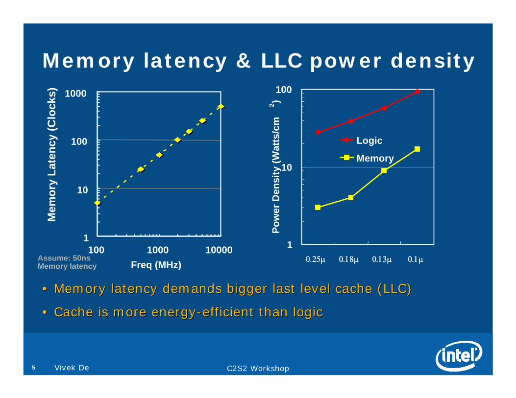
Memory latency & LLC power density
1
10
100
1000
100 1000 10000Freq (MHz)
Mem
ory
Late
ncy
(Clo
cks)
Assume: 50ns Memory latency
1
10
100
0.25μ 0.18μ 0.13μ 0.1μ
Pow
er D
ensi
ty (W
atts
/cm
2 )
Logic
Memory
•• Memory latency demands bigger last level cache (LLC)Memory latency demands bigger last level cache (LLC)
•• Cache is more energyCache is more energy--efficient than logicefficient than logic

C2S2 Workshop6 Vivek De
LLC integration trends
0%
25%
50%
75%
100%
1u 0.5u 0.25u 0.13u 65nm
Cac
he %
of T
otal
Are
a
486 Pentium®
Pentium® III
Pentium® 4
Pentium® M
•• LLC area approaching 50% in desktop & mobile processorsLLC area approaching 50% in desktop & mobile processors
•• LLC area approaching 80% in server processorsLLC area approaching 80% in server processors
Desktop & mobile processors Server processors

C2S2 Workshop7 Vivek De
SRAM cell design trends
•• Improve CD control by unidirectional polyImprove CD control by unidirectional poly
•• Relax critical layer patterning requirementsRelax critical layer patterning requirements
•• Optimizing design rules is keyOptimizing design rules is key
•• Shorter bitline enables better cycle time and/or array efficienShorter bitline enables better cycle time and/or array efficiencycy
•• Full metal wordline with wider pitch achieves better RCFull metal wordline with wider pitch achieves better RC
Cell on 90nm(1um2)
Cell on 65nm(0.57um2)
0.46x1.24um
IEDM’02
C2S2 Workshop8 Vivek De
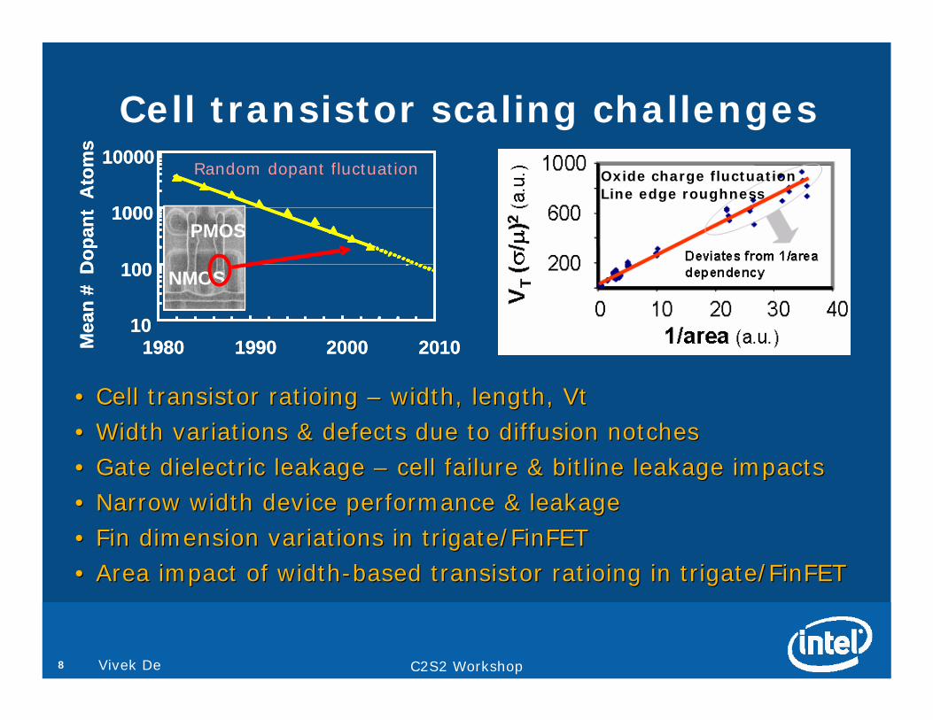
Cell transistor scaling challenges
10
100
1000
10000
1980 1990 2000 2010Mea
n #
Dop
ant
Ato
ms
PMOS
NMOS
10
100
1000
10000
1980 1990 2000 2010Mea
n #
Dop
ant
Ato
ms
PMOS
NMOS
Random dopant fluctuation Oxide charge fluctuationLine edge roughness
•• Cell transistor ratioing Cell transistor ratioing –– width, length, Vtwidth, length, Vt
•• Width variations & defects due to diffusion notchesWidth variations & defects due to diffusion notches
•• Gate dielectric leakage Gate dielectric leakage –– cell failure & bitline leakage impactscell failure & bitline leakage impacts
•• Narrow width device performance & leakageNarrow width device performance & leakage
•• Fin dimension variations in trigate/FinFETFin dimension variations in trigate/FinFET
•• Area impact of widthArea impact of width--based transistor ratioing in trigate/FinFETbased transistor ratioing in trigate/FinFET
C2S2 Workshop9 Vivek De
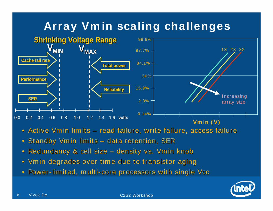
Array Vmin scaling challengesShrinking Voltage RangeShrinking Voltage Range
0.0 0.2 0.4 0.6 0.8 1.0 1.2 1.4 1.6 voltsvolts
Cache fail rateCache fail rate
PerformancePerformance
SERSER
Total powerTotal power
ReliabilityReliability
VVMAXMAXVVMINMINShrinking Voltage RangeShrinking Voltage Range
0.0 0.2 0.4 0.6 0.8 1.0 1.2 1.4 1.6 voltsvolts
Cache fail rateCache fail rate
PerformancePerformance
SERSER
Total powerTotal power
ReliabilityReliability
VVMAXMAXVVMINMIN
50%
84.1%
97.7%
99.9%
15.9%
2.3%
0.14%
Vmin (V)
Increasing array size
1X 2X 3X
•• Active Vmin limits Active Vmin limits –– read failure, write failure, access failureread failure, write failure, access failure
•• Standby Vmin limits Standby Vmin limits –– data retention, SERdata retention, SER
•• Redundancy & cell size Redundancy & cell size –– density vs. Vmin knobdensity vs. Vmin knob
•• Vmin degrades over time due to transistor agingVmin degrades over time due to transistor aging
•• PowerPower--limited, multilimited, multi--core processors with single Vcccore processors with single Vcc

C2S2 Workshop10 Vivek De
Erratic bit failures
Increased sampling
•• Need more complex error detection & correction schemesNeed more complex error detection & correction schemes
•• Dynamic Pellston engine for cache line disablingDynamic Pellston engine for cache line disabling
•• Additional density & performance impactsAdditional density & performance impacts
C2S2 Workshop11 Vivek De
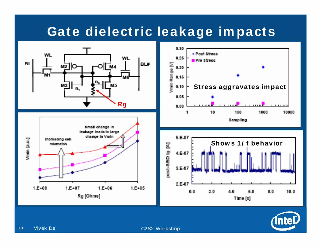
Gate dielectric leakage impacts
Stress aggravates impact
Shows 1/f behavior
Rg

C2S2 Workshop12 Vivek De
Performance impact of bitline leakage
Courtesy: K. Agawa et al., JSSC, May 2001
•• Reduced effective cell currentReduced effective cell current•• Negative bitline swing developmentNegative bitline swing development
Need to use bitline leakage compensation & reduction techniquesNeed to use bitline leakage compensation & reduction techniques

C2S2 Workshop13 Vivek De
Dual-Vcc + dynamic sleep
Embedded level Embedded level shifters for wordline & shifters for wordline & write drivers minimize write drivers minimize area & power overheadarea & power overhead
Push active Vmin limit to VmaxPush active Vmin limit to Vmax
Reduce idle power:Reduce idle power:NMOS sleep with NMOS sleep with passive clamppassive clamp
Reduce idle power:Reduce idle power:PMOS sleep with PMOS sleep with passive clamppassive clamp

C2S2 Workshop14 Vivek De
Sleep transistor with active clamp
C2S2 Workshop15 Vivek De
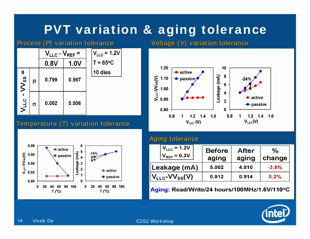
PVT variation & aging toleranceProcess (P) variation toleranceProcess (P) variation tolerance
Temperature (T) variation toleranceTemperature (T) variation tolerance
Voltage (V) variation toleranceVoltage (V) variation tolerance
Aging toleranceAging tolerance

C2S2 Workshop16 Vivek De
Multi-Vcc cell & array design
•• MultiMulti--Vcc generation, control, distribution & timing overheadVcc generation, control, distribution & timing overhead
•• Differential noises among multiple VccDifferential noises among multiple Vcc’’s impact cell failures impact cell failure
•• Partial write & pseudoPartial write & pseudo--read supportread support
Optimum voltage choicesOptimum voltage choices
Vmax: Max Vcc, Va: Min Vcc
Improved static noise Improved static noise margin (SNM) for readmargin (SNM) for read
Improved write noise Improved write noise margin (WNM)margin (WNM)
C2S2 Workshop17 Vivek De
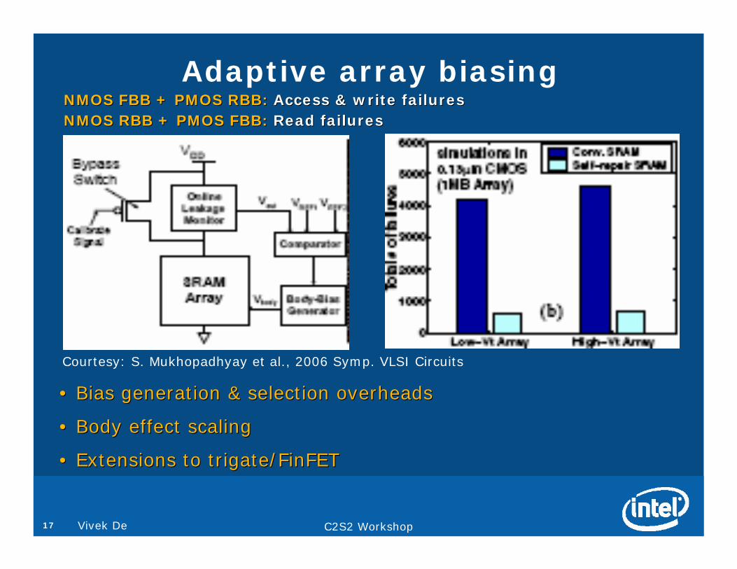
Adaptive array biasing
•• Bias generation & selection overheadsBias generation & selection overheads
•• Body effect scalingBody effect scaling
•• Extensions to trigate/FinFETExtensions to trigate/FinFET
NMOS FBB + PMOS RBB:NMOS FBB + PMOS RBB: Access & write failuresAccess & write failuresNMOS RBB + PMOS FBB:NMOS RBB + PMOS FBB: Read failuresRead failures
Courtesy: S. Mukhopadhyay et al., 2006 Symp. VLSI Circuits

C2S2 Workshop18 Vivek De
Cell stability: static vs. dynamicStatic read failure Static read failure (conservative)(conservative)
Dynamic read failure Dynamic read failure (realistic)(realistic)
Wordline
Static write failure Static write failure (optimistic)(optimistic)
Wordline
Dynamic write failure Dynamic write failure (realistic)(realistic)
Need to comprehend realistic dynamic stability in statistical Need to comprehend realistic dynamic stability in statistical failure rate analysis & array Vmin measurementsfailure rate analysis & array Vmin measurements
C2S2 Workshop19 Vivek De
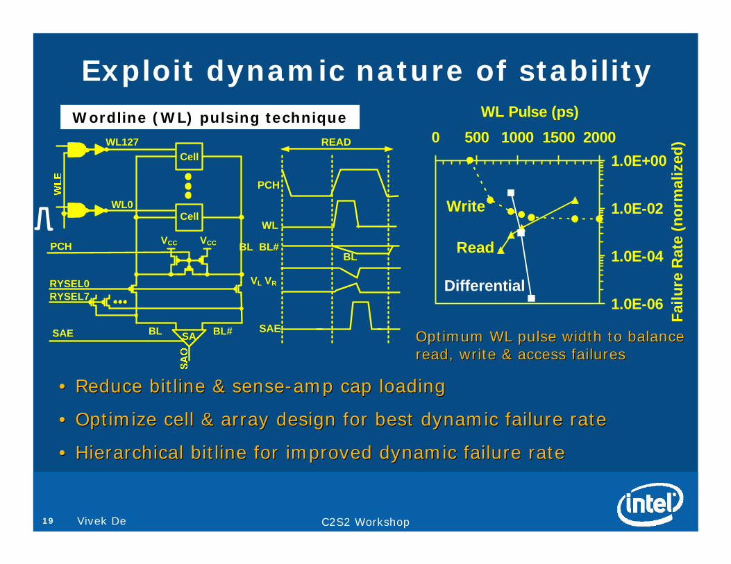
Exploit dynamic nature of stability
1.0E-06
1.0E-04
1.0E-02
1.0E+000 500 1000 1500 2000
WL Pulse (ps)
Failu
re R
ate
(nor
mal
ized
)
Read
Write
Differential
SAE
PCH
SABL BL#
RYSEL0RYSEL7
VCCVCC
Cell
Cell
WL127
WL0
WL
BL
SAE
BL BL#
READ
PCH
VL VR
Wordline (WL) pulsing technique
Optimum WL pulse width to balance Optimum WL pulse width to balance read, write & access failuresread, write & access failures
•• Reduce bitline & senseReduce bitline & sense--amp cap loadingamp cap loading
•• Optimize cell & array design for best dynamic failure rateOptimize cell & array design for best dynamic failure rate
•• Hierarchical bitline for improved dynamic failure rateHierarchical bitline for improved dynamic failure rate
C2S2 Workshop20 Vivek De
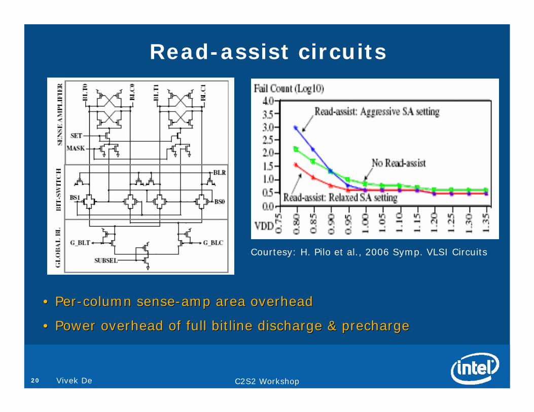
Read-assist circuits
•• PerPer--column sensecolumn sense--amp area overheadamp area overhead
•• Power overhead of full bitline discharge & prechargePower overhead of full bitline discharge & precharge
Courtesy: H. Pilo et al., 2006 Symp. VLSI Circuits
C2S2 Workshop21 Vivek De
Performance & power improvement•• Optimize senseOptimize sense--amp (SA) for input offset, loading, speed & areaamp (SA) for input offset, loading, speed & area
•• AC offset improvement AC offset improvement –– bitline segmentation & SA strobe controlbitline segmentation & SA strobe control
•• Bitline decoupled senseBitline decoupled sense--amp amp –– reduce timing complexityreduce timing complexity
•• SA offset compensation SA offset compensation –– cycle time vs. latencycycle time vs. latency
•• Asynchronous array design Asynchronous array design –– latency vs. complexitylatency vs. complexity
•• Dynamic IntelDynamic Intel® smart cache sizing smart cache sizing – Predict cache usage requirement– Dynamically adapt effective cache size– Re-power on demand to deliver full performance
C2S2 Workshop22 Vivek De
Research opportunities
•• Dynamic multiDynamic multi--Vcc & other circuit techniquesVcc & other circuit techniques
•• Vmin tracking for PVT variations & agingVmin tracking for PVT variations & aging
•• Resilient techniques for access failuresResilient techniques for access failures
•• Adaptive cache size, cycle time & latencyAdaptive cache size, cycle time & latency
•• Application of cache compression techniquesApplication of cache compression techniques
•• Cache hierarchy, size & performance needsCache hierarchy, size & performance needs
Top Related