


Languages
Pages
Legal

M. Shojaei SMDP-AMS VLSI Design, GEC-Goa March 2009
SMDP Workshop on Mixed-Signal VLSI Design, GEC, Goa
M. Shojaei Baghini, Assistant Prof.
Dept. of Electrical Engineering
IIT-Bombay
Comparators, Gm-C Filters, SC Filters in CMOS Technology

M. Shojaei SMDP-AMS VLSI Design, GEC-Goa March 2009
Materials presented in this workshop are partly from the following references.
CMOS Analog Circuit Design by P. E. Allen et al. , Oxford University Press, 2002.
CMOS Circuit Design, Layout, and Simulation by R. J. Baker et al, IEEE press, reprint 2002, edition 1998.
CMOS Mixed-Signal Circuit Design by R. J. Baker, reprint 2008, edition 2002, Wiley.
Analog Integrated Circuit Design by D. Johns et al. Wiley, edition 2005.
M. Shojaei SMDP-AMS VLSI Design, GEC-Goa March 2009
Teaching Methodology
The presented lecture is based on a combination of slide presentation, class notes and lab experiments.
M. Shojaei SMDP-AMS VLSI Design, GEC-Goa March 2009
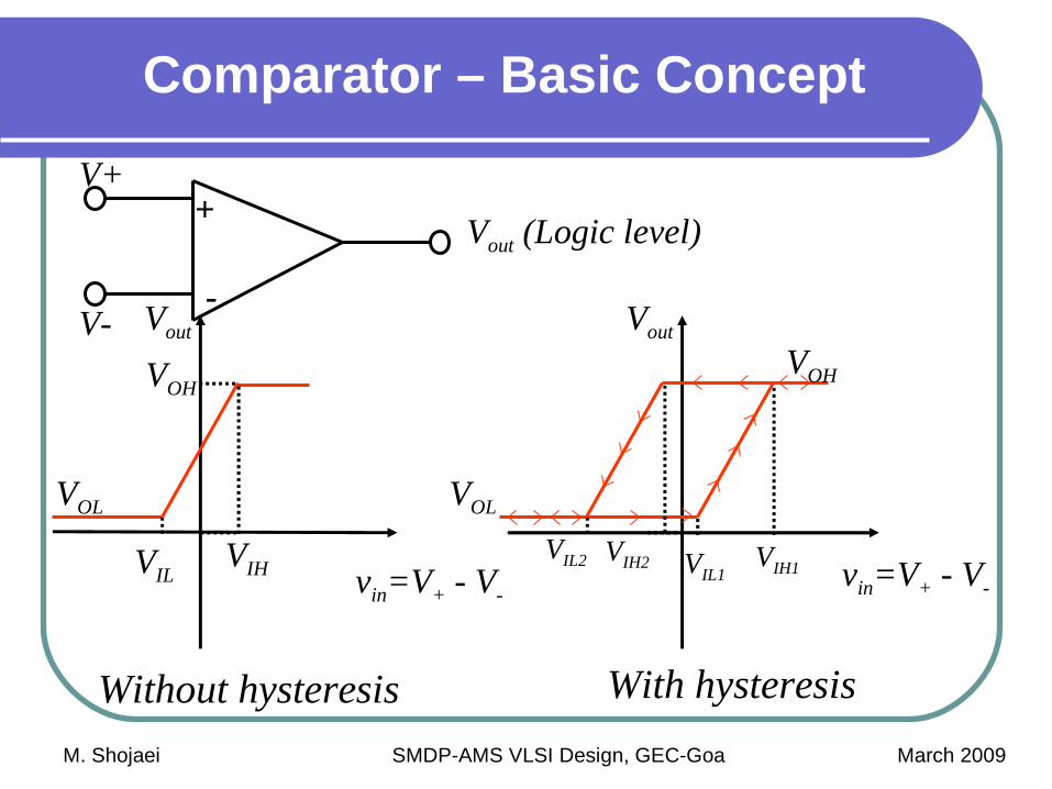
Comparator – Basic Concept
+
-
V+
V-
Vout (Logic level)
vin=V+ - V-
Vout
VOH
VOL
VIHVIL vin=V+ - V-
Vout
VOH
VOL
VIH1VIL1VIL2 VIH2
Without hysteresis With hysteresis

M. Shojaei SMDP-AMS VLSI Design, GEC-Goa March 2009
Comparator – Important specifications
• Gain Resolution• Delay Switching speed• Power dissipation• Input common-mode range• Offset voltage• Input noise voltage
M. Shojaei SMDP-AMS VLSI Design, GEC-Goa March 2009
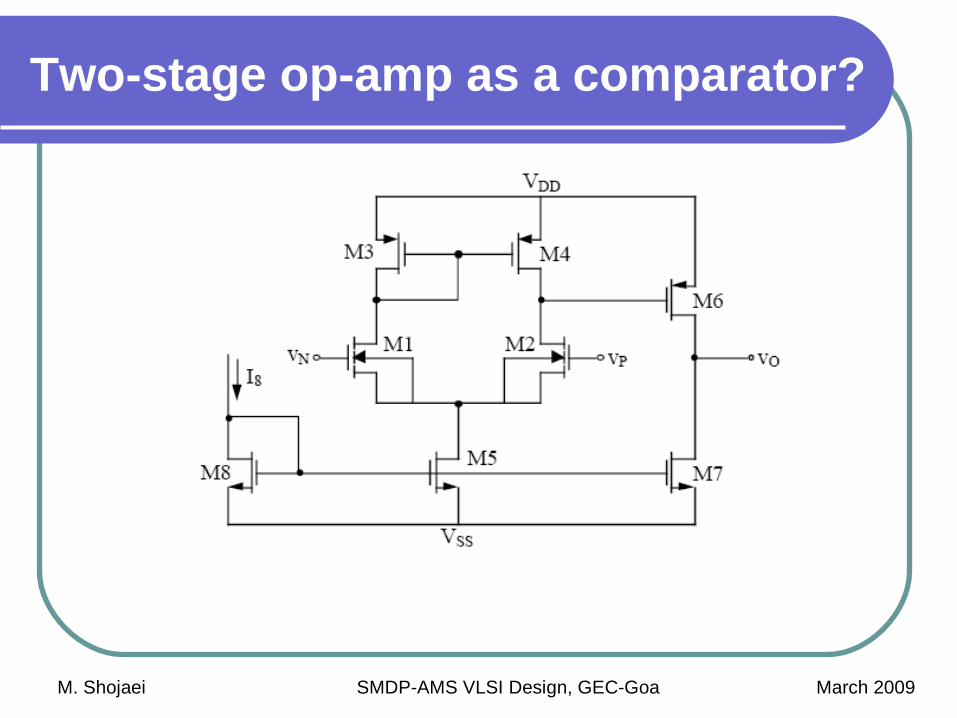
Two-stage op-amp as a comparator?

M. Shojaei SMDP-AMS VLSI Design, GEC-Goa March 2009
Folded cascode op-amp as a Comparator?
Gain & Delay are important specifications of a comparator.
M. Shojaei SMDP-AMS VLSI Design, GEC-Goa March 2009
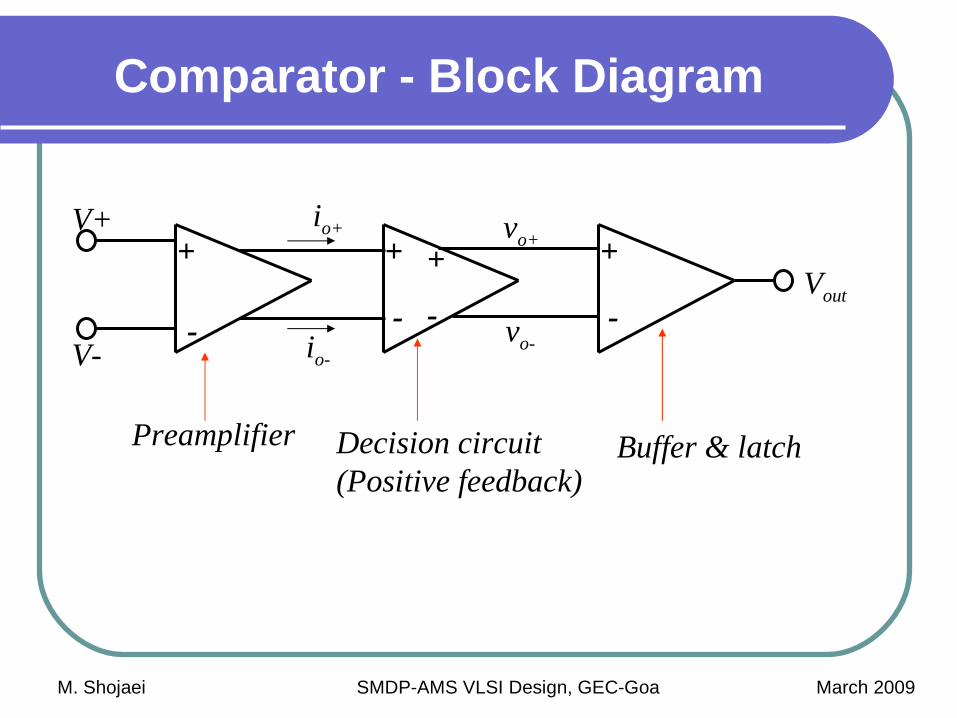
Comparator - Block Diagram
+
-
V+
V-
+
-
+
-
io+
io-
+
-
vo+
vo-
Vout
Preamplifier Decision circuit(Positive feedback)
Buffer & latch

M. Shojaei SMDP-AMS VLSI Design, GEC-Goa March 2009
Vin+Vin-
M1 M2
M3M4 M5
Iout-
Comparator – Preamplifier example
M6
Iout+
( )−++
−⋅+= ininss
out VVGmI
I 12
2
11
3
6 gm
LWL
W
Gm ⋅
=
56
=
L
W
L
W
21
=
L
W
L
W
43
=
L
W
L
W( )−+−
−⋅−= ininss
out VVGmI
I 12
All nodes except output Node are low-impedance.
M. Shojaei SMDP-AMS VLSI Design, GEC-Goa March 2009
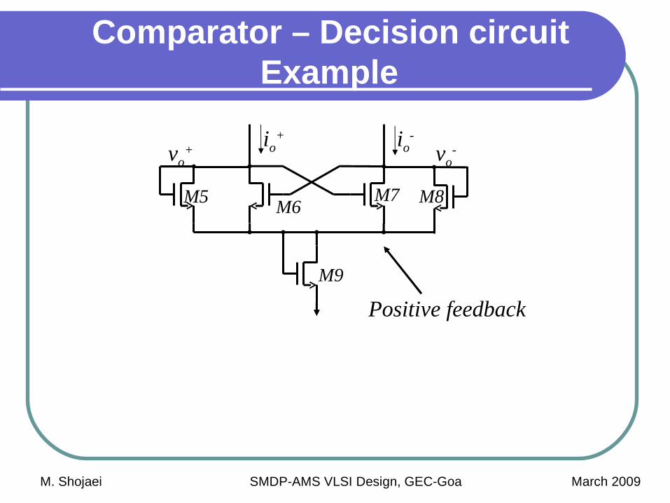
Comparator – Decision circuit Example
M5M6
M8M7
M9
io+ io
-
vo+ vo
-
Positive feedback
M. Shojaei SMDP-AMS VLSI Design, GEC-Goa March 2009
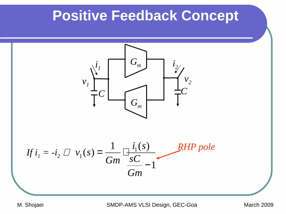
Gm
Gm
C C
i1i2
Positive Feedback Concept
If i1 = -i2 ⇒1
)(1)( 1
1
−⋅=
GmsC
si
Gmsv
v1v2
RHP pole

M. Shojaei SMDP-AMS VLSI Design, GEC-Goa March 2009
Comparator – An example output buffer
Vin+Vin
-
Vout
M1M2
M3 M4
M5
M6Self-biased differential amplifier
High-speed comparators typically use track-and-latch mechanism for the stage after preamplifier.

M. Shojaei SMDP-AMS VLSI Design, GEC-Goa March 2009
More details will be given in the lecture.

M. Shojaei SMDP-AMS VLSI Design, GEC-Goa March 2009
Gm-C FiltersApplication in continuous time filters (DSL/ADSL, Video applications, very low-
frequency applications…)
Need for some sort of tuning circuitry
Linearity requirements
Noise performance

M. Shojaei SMDP-AMS VLSI Design, GEC-Goa March 2009
Basic building block of Gm-C filters
Integrator is the main building block of continuous time filters.
+
-Gm
C
Rout=∞Rin=∞
+
-
vin
⋅=
m
inout
GCs
vvvout
Gm/C: Unity gain frequency of the integrator
M. Shojaei SMDP-AMS VLSI Design, GEC-Goa March 2009
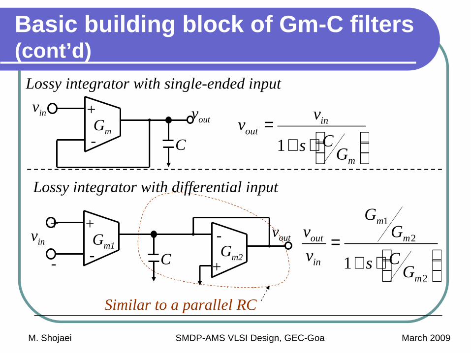
Basic building block of Gm-C filters (cont’d)
+
-Gm
C
vin
⋅+=
m
inout
GCs
vv
1
Lossy integrator with single-ended input
vout
+
-Gm1
C
vin
⋅+=
2
2
1
1m
m
m
in
out
GCs
GG
v
v
Lossy integrator with differential input
-
+Gm2
+
-
Similar to a parallel RC
vout

M. Shojaei SMDP-AMS VLSI Design, GEC-Goa March 2009
Fully differential Gm-C integrator
+
-Gm C
+
-
vin vout
+
-
+
-Gm 2C
+
-
vout
+
-2C
vin
Which configuration is preferred?

M. Shojaei SMDP-AMS VLSI Design, GEC-Goa March 2009
Differential architecture needs common-mode feedback (CMFB)
Example
Iref1
Vin+ Vin-Iref2 M1 M2
M3M4
M5 M6
M7Vout-diff
Vin-M1 M2
M3M4
M5 M6
Vout+
-
Quiescent value of CM output voltage is very sensitive to “Iref1-Iref2”.
Iref1
Internal CMFB!
M. Shojaei SMDP-AMS VLSI Design, GEC-Goa March 2009
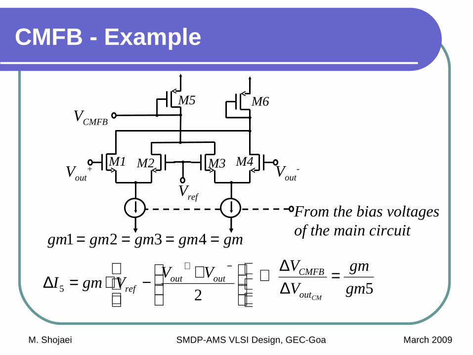
CMFB - Example
Vref
Vout+ Vout
-
From the bias voltages of the main circuit
VCMFB
M1 M2 M3 M4
M5 M6
gmgmgmgmgm ==== 4321
+−⋅=∆−+
25outout
ref
VVVgmI 5gm
gm
V
V
CMout
CMFB =∆∆⇒
M. Shojaei SMDP-AMS VLSI Design, GEC-Goa March 2009
More details will be given in the lecture.
M. Shojaei SMDP-AMS VLSI Design, GEC-Goa March 2009
Switched-Capacitor (SC) Filters
SC filters are discrete-time or sampled-data equivalents of continuous-time filters.
SC circuits eliminate resistors in filters by replacing them with capacitors and switches.
Filter time constants are a function of capacitor ratios and clock frequency.
M. Shojaei SMDP-AMS VLSI Design, GEC-Goa March 2009
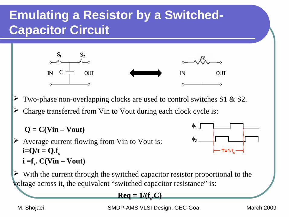
Emulating a Resistor by a Switched-Capacitor Circuit
Two-phase non-overlapping clocks are used to control switches S1 & S2.
Charge transferred from Vin to Vout during each clock cycle is: Q = C(Vin – Vout)
Average current flowing from Vin to Vout is: i=Q/t = Q.fs i =fs. C(Vin – Vout)
With the current through the switched capacitor resistor proportional to the voltage across it, the equivalent “switched capacitor resistance” is:
Req = 1/(fs.C)

M. Shojaei SMDP-AMS VLSI Design, GEC-Goa March 2009
Switched-capacitor Circuits: Integrator
For fsignal << fsampling Vo =
ωo = fs x (Cs / CI )
EECS 247 Course slides, UCB

M. Shojaei SMDP-AMS VLSI Design, GEC-Goa March 2009
More details will be given in the lecture.
Top Related