


Languages
Pages
Legal

This document is confidential and is proprietary to the American Chemical Society and its authors. Do not copy or disclose without written permission. If you have received this item in error, notify the sender and delete all copies.
Silicon-based Single Quantum Dot Emission in the Telecoms
C-band
Journal: ACS Photonics
Manuscript ID ph-2017-00276x.R1
Manuscript Type: Article
Date Submitted by the Author: n/a
Complete List of Authors: Orchard, Jonathan; The University of Sheffield, Department of Physics and Astronomy Woodhead, Christopher; Lancaster University
Wu, Jiang; University College London, Electronic and Electrical Engineering Tang, Mingchu; University College London, Electronic and Electrical Engineering Beanland, Richard; University of Warwick, Noori, Yasir; Lancaster University, Physics Liu, Huiyun; University College London, Department of Electronic and Electrical Engineering Young, Robert; Lancaster University, Physics Mowbray, David; The University of Sheffield, Physics and Astronomy
ACS Paragon Plus Environment
ACS PhotonicsCORE Metadata, citation and similar papers at core.ac.uk
Provided by Lancaster E-Prints
Silicon-based Single Quantum Dot Emission in the Telecoms C-band Jonathan R. Orchard1, Chris Woodhead2, Jiang Wu3, Mingchu Tang3, Richard Beanland4, Yasir Noori2, Huiyun Liu3, Robert J. Young2 and David J. Mowbray1
1Department of Physics, University of Sheffield, Hicks Building, Hounsfield Road, Sheffield S3 7RH, United
Kingdom 2Department of Physics, University of Lancaster, Lancaster LA1 4YB, United Kingdom 3Department of Electronic & Electrical Engineering, University College London, Torrington Place, London
WC1E 7JE United Kingdom 4Department of Physics, University of Warwick, Gibbet Hill Road, Coventry CV4 7AL, United Kingdom
ABSTRACT: We report the observation of single quantum dot (QD) emission in the telecoms C-band
(1530 – 1565 nm) from an InAs QD structure grown on a Si substrate. A large red-shift of the emission
is achieved by capping InAs QDs with a thin GaAsSb layer. Sharp lines, representing emission from
single QDs, are observed out to wavelengths as long as 1540 nm. Comparison is made to the optical
properties of a nominally identical active region structure grown on a GaAs substrate. Single QD
emission from a Si based system at 1500 nm has the potential for single photon sources compatible
with current optical fibres and reduced complexity of integration with drive electronics.
KEYWORDS: single-photon sources, quantum dots, Si substrate, C-band, III-V semiconductors,
GaAsSb
The unique, discrete electronic density of states exhibited by semiconductor quantum dots (QDs)
provides many applications for both conventional and novel light emitters. An example of the latter is
the single photon source, with application in the field of quantum cryptography. Here a single QD is
loaded optically or electrically with a quasi-random number of excitons. Because the photon energy
resulting from a recombining exciton is dependent on the number of excitons remaining in the dot,
subsequent radiative decay of the excitons gives rise to a sequence of photons, each exhibiting a
different energy. The photon produced by the recombination of the final exciton can be spectrally
selected; hence giving exactly one photon for each excitation event, independent of the number of
excitons initially excited1. Semiconductor QDs therefore provide highly compact and efficient on-
demand sources of single photons.
Whilst GaAs-based QD single photon sources at 900~1300 nm2-4
and InP-based sources in the
telecoms C-band at 1550 nm5 have been demonstrated, a Si-based C-band source, allowing direct
integration with Si-based drive electronics, is highly desirable. Extension of the emission wavelength
from QDs grown within a GaAs matrix has been demonstrated by capping InAs QDs with a thin
GaAsSb layer; room temperature emission out to ~1600 nm has been achieved.6-23
Detailed structural
studies reveal that capping InAs QDs with GaAsSb prevents the decomposition observed when capping
with GaAs. GaAsSb capped QDs were found to have a height approximately twice that of GaAs
capped dots; the lateral sizes appeared to be very similar. The initial height of the QDs was found to be
retained for a Sb composition greater than 14%.22
This suppression of the decomposition was attributed
to the reduced lattice mis-match between InAs and GaAsSb, compared to InAs and GaAs.11 In
addition, it is well documented that capping QDs with a strain reducing layer (for example InGaAs but
also GaAsSb) results in a red shift of the emission.23
A third mechanism contributing to the extension
of the emission wavelength is a transition to a type-II system for Sb compositions above ~14%,6,8,13,17,23
with the hole localized in the GaAsSb two-dimensional layer and the electron in the QD. Related to the
structures studied in the present work are GaSb QDs and quantum rings grown in a GaAs matrix.24-31
These also form a type-II system but with the electrons localized in the GaAs and holes in the QD or
ring.25,29
Emission wavelengths around ~1.3 µm are typically observed.24,25,27
In this paper we report the observation of single QD emission at wavelengths as long as 1540 nm from
InAs QDs capped with a 6 nm GaAs0.74Sb0.26 layer and grown directly on a Si substrate. As the number
of QDs probed decreases, the inhomogeneously broadened emission breaks up into a small number of
sharp lines, each line corresponding to emission from excitons localized in different QDs. Comparison
Page 1 of 9
ACS Paragon Plus Environment
ACS Photonics
123456789101112131415161718192021222324252627282930313233343536373839404142434445464748495051525354555657585960
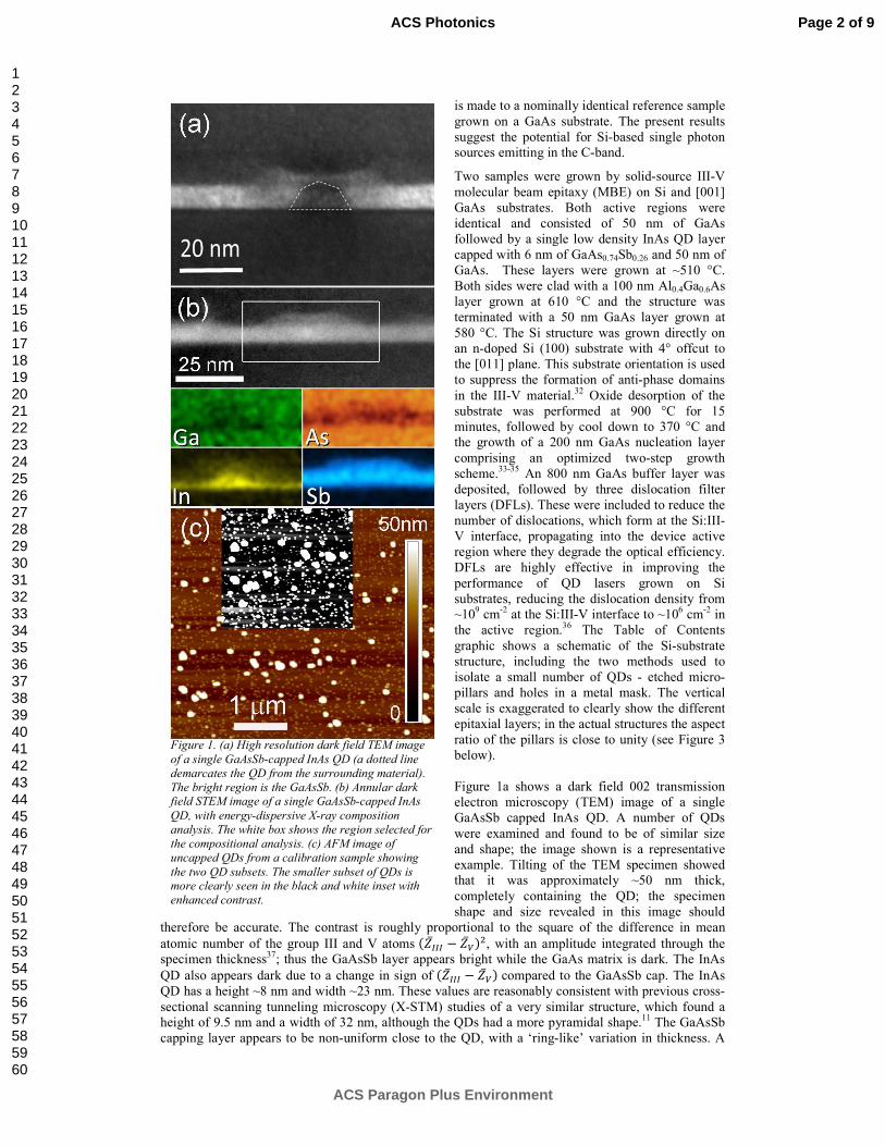
Figure 1. (a) High resolution dark field TEM image
of a single GaAsSb-capped InAs QD (a dotted line
demarcates the QD from the surrounding material).
The bright region is the GaAsSb. (b) Annular dark field STEM image of a single GaAsSb-capped InAs
QD, with energy-dispersive X-ray composition
analysis. The white box shows the region selected for
the compositional analysis. (c) AFM image of
uncapped QDs from a calibration sample showing
the two QD subsets. The smaller subset of QDs is more clearly seen in the black and white inset with
enhanced contrast.
is made to a nominally identical reference sample
grown on a GaAs substrate. The present results
suggest the potential for Si-based single photon
sources emitting in the C-band.
Two samples were grown by solid-source III-V
molecular beam epitaxy (MBE) on Si and [001]
GaAs substrates. Both active regions were
identical and consisted of 50 nm of GaAs
followed by a single low density InAs QD layer
capped with 6 nm of GaAs0.74Sb0.26 and 50 nm of
GaAs. These layers were grown at ~510 °C.
Both sides were clad with a 100 nm Al0.4Ga0.6As
layer grown at 610 °C and the structure was
terminated with a 50 nm GaAs layer grown at
580 °C. The Si structure was grown directly on
an n-doped Si (100) substrate with 4° offcut to
the [011] plane. This substrate orientation is used
to suppress the formation of anti-phase domains
in the III-V material.32
Oxide desorption of the
substrate was performed at 900 °C for 15
minutes, followed by cool down to 370 °C and
the growth of a 200 nm GaAs nucleation layer
comprising an optimized two-step growth
scheme.33-35
An 800 nm GaAs buffer layer was
deposited, followed by three dislocation filter
layers (DFLs). These were included to reduce the
number of dislocations, which form at the Si:III-
V interface, propagating into the device active
region where they degrade the optical efficiency.
DFLs are highly effective in improving the
performance of QD lasers grown on Si
substrates, reducing the dislocation density from
~109 cm
-2 at the Si:III-V interface to ~10
6 cm
-2 in
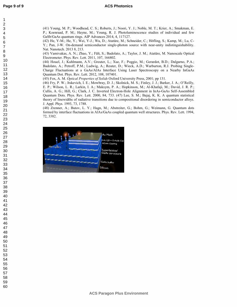
the active region.36 The Table of Contents
graphic shows a schematic of the Si-substrate
structure, including the two methods used to
isolate a small number of QDs - etched micro-
pillars and holes in a metal mask. The vertical
scale is exaggerated to clearly show the different
epitaxial layers; in the actual structures the aspect
ratio of the pillars is close to unity (see Figure 3
below).
Figure 1a shows a dark field 002 transmission
electron microscopy (TEM) image of a single
GaAsSb capped InAs QD. A number of QDs
were examined and found to be of similar size
and shape; the image shown is a representative
example. Tilting of the TEM specimen showed
that it was approximately ~50 nm thick,
completely containing the QD; the specimen
shape and size revealed in this image should
therefore be accurate. The contrast is roughly proportional to the square of the difference in mean
atomic number of the group III and V atoms ��̅��� � �̅���, with an amplitude integrated through the
specimen thickness37; thus the GaAsSb layer appears bright while the GaAs matrix is dark. The InAs
QD also appears dark due to a change in sign of ��̅��� � �̅�� compared to the GaAsSb cap. The InAs
QD has a height ~8 nm and width ~23 nm. These values are reasonably consistent with previous cross-
sectional scanning tunneling microscopy (X-STM) studies of a very similar structure, which found a
height of 9.5 nm and a width of 32 nm, although the QDs had a more pyramidal shape.11
The GaAsSb
capping layer appears to be non-uniform close to the QD, with a ‘ring-like’ variation in thickness. A
Page 2 of 9
ACS Paragon Plus Environment
ACS Photonics
123456789101112131415161718192021222324252627282930313233343536373839404142434445464748495051525354555657585960
similar structure was observed in cross-sectional scanning tunneling microscopy (X-STM)11 for
samples where the GaAsSb was grown at 500 °C. This was attributed to migration of material away
from the apex of the dot, hence minimizing the strain.
Figure 1b shows an annular dark field (ADF) scanning TEM image of a second GaAsSb capped InAs
QD along with energy-dispersive X-ray spectroscopy (EDX) composition maps of the elements Ga, As
In and Sb. Contrast in the ADF-STEM image increases with atomic number, and the QD appears only
slightly brighter than the surrounding material. The QD/cap interface in the In map is diffuse, making it
difficult to accurately determine the QD height;
the In composition profile indicates a value
between 6.5 and 9.5 nm. Away from the QD the
GaAsSb layer has a thickness of ~5-6 nm,
consistent with a value of 6 nm estimated from
the growth conditions. The In map reveals a
non-zero In composition in the nominal
GaAsSb capping layer, a result of In diffusion
or segregation during growth. The
incorporation of In will reduce the band gap of
this layer.
Figure 1c shows an atomic force microscopy
(AFM) image of an uncapped layer of QDs
grown under the same conditions as the capped
QDs used for optical studies. Visible in the
image are two subsets of QDs. The distribution
of the large QDs exhibits a significant spatial
variation with a low average density, estimated
to be of order 5 µm-2
. These dots also exhibit a
broad size distribution. The subset of smaller
QDs has a much larger density ~80 µm-2
. We
show below that the larger QDs are responsible
for emission in the 1500 nm spectral region.
The structural images shown in Figures 1a and
b were obtained for a sample grown on a GaAs
substrate, the AFM image is for growth on Si.
Previous structural studies of QDs grown on
both Si and GaAs substrates have shown no
significant differences in both shape, size and
density. This is expected as a large thickness (>
1 µm) of GaAs is deposited on the Si substrate
before the QDs are grown. In addition, optical
studies have revealed the QDs to have very
similar properties apart from a small energy
shift of the emission for QDs grown on a Si
substrate. 36
This shift is attributed to residue
strain (0.24% at a temperature of 77 K) which
results from the different III-V and Si thermal expansion coefficients and cool down following growth. 36 In the optical data present below, both sets of QDs emit at essentially the same wavelengths for the
Si and GaAs substrate samples, confirming very similar physical structures.
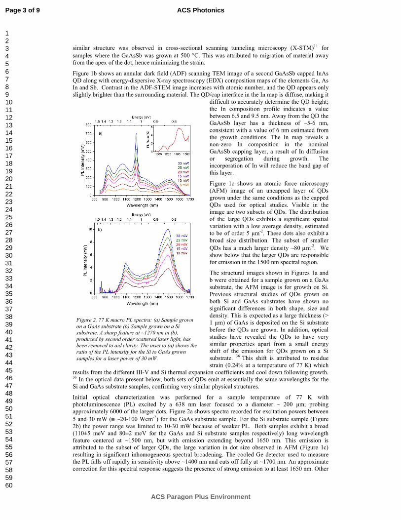
Initial optical characterization was performed for a sample temperature of 77 K with
photoluminescence (PL) excited by a 638 nm laser focused to a diameter ~ 200 µm; probing
approximately 6000 of the larger dots. Figure 2a shows spectra recorded for excitation powers between
5 and 30 mW (≡ ~20-100 Wcm-2) for the GaAs substrate sample. For the Si substrate sample (Figure
2b) the power range was limited to 10-30 mW because of weaker PL. Both samples exhibit a broad
(110±5 meV and 80±2 meV for the GaAs and Si substrate samples respectively) long wavelength
feature centered at ~1500 nm, but with emission extending beyond 1650 nm. This emission is
attributed to the subset of larger QDs, the large variation in dot size observed in AFM (Figure 1c)
resulting in significant inhomogeneous spectral broadening. The cooled Ge detector used to measure
the PL falls off rapidly in sensitivity above ~1400 nm and cuts off fully at ~1700 nm. An approximate
correction for this spectral response suggests the presence of strong emission to at least 1650 nm. Other
Figure 2. 77 K macro PL spectra: (a) Sample grown
on a GaAs substrate (b) Sample grown on a Si
substrate. A sharp feature at ~1270 nm in (b),
produced by second order scattered laser light, has
been removed to aid clarity. The inset to (a) shows the
ratio of the PL intensity for the Si to GaAs grown
samples for a laser power of 30 mW.
Page 3 of 9
ACS Paragon Plus Environment
ACS Photonics
123456789101112131415161718192021222324252627282930313233343536373839404142434445464748495051525354555657585960
features present in Figure 2a are emission from the InAs wetting layer at ~920 nm, the subset of
smaller QDs at 1070 nm and the GaAsSb capping layer at ~1200 nm. The estimated GaAsSb band gap
for 26% Sb is 1204 nm, very close to the measured value.38
The emission from the subset of smaller
QD is brighter than that of the larger QDs, in agreement with their relative densities (Figure 1c).
Previous studies of similar structures show only the long wavelength emission,7,8 indicating a single set
of QDs. Structural studies of these samples11
reveal QD parameters very similar to those determined
from the present TEM and STEM measurements, indicating that the dots shown in Figure 1 give rise to
the long wavelength emission at ~1500 nm.
The long wavelength QD emission from the Si substrate sample (Figure 2b) is ~20 weaker in
comparison to the GaAs sample. This is attributed to dislocations reaching the active region where they
act as non-radiative centers. These have a much larger effect on emission from the InAs wetting and
GaAsSb capping layers as captured carriers are able to migrate in-plane until they reach a dislocation.
No emission is observed from either layer in the Si substrate sample. In contrast, although the QD
emission is reduced in intensity it is still visible because carrier capture by a QD inhibits subsequent
migration to a dislocation.39
In contrast to the GaAs substrate sample, emission from the lower density,
larger QDs is more intense than that of the higher density, smaller QDs. This most likely reflects the
much deeper confining potential of the larger QDs, which provides a strong barrier preventing carrier
migration to dislocations. The differing behavior of the QD and bulk/2D layers is demonstrated in the
inset to Figure 2a which plots the PL intensity ratio of the Si/GaAs samples for a laser power of 30
mW. Although the ratio is always less than unity, peaks
are observed at ~1100 and ~1500 nm, corresponding to
emission from the two subsets of QDs, demonstrating
their reduced sensitivity to non-radiative defects. The
optical efficiency of the Si substrate sample could be
increased by including annealing steps during growth to
further improve the effectiveness of the DFLs; this has
been shown to significantly increase the optical
efficiency of test structures and the performance of QD
lasers.36
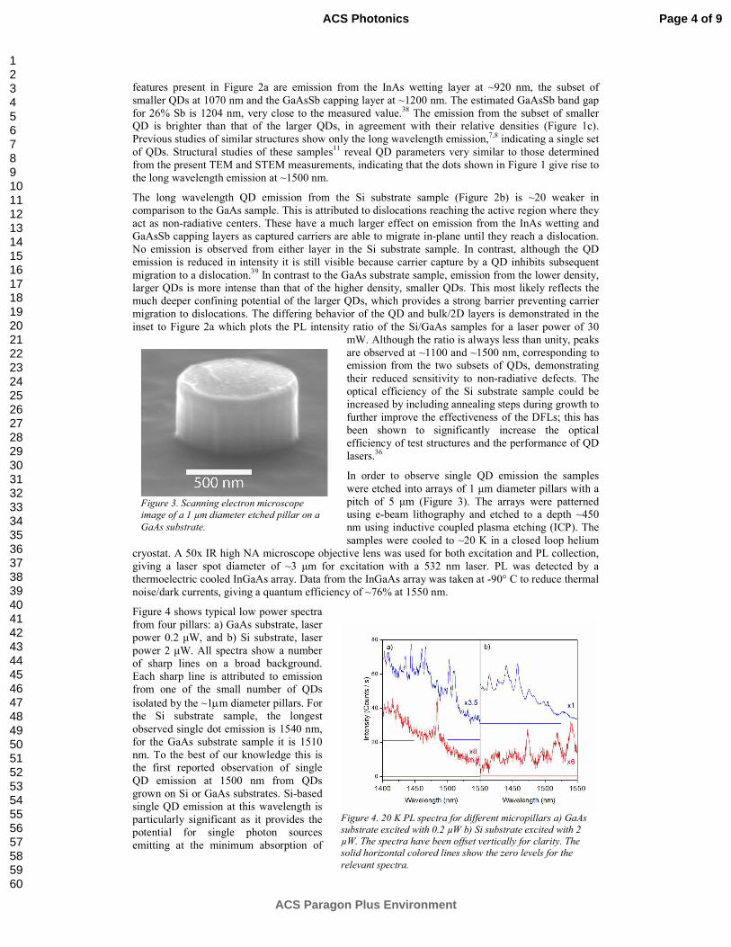
In order to observe single QD emission the samples
were etched into arrays of 1 µm diameter pillars with a
pitch of 5 µm (Figure 3). The arrays were patterned
using e-beam lithography and etched to a depth ~450
nm using inductive coupled plasma etching (ICP). The
samples were cooled to ~20 K in a closed loop helium
cryostat. A 50x IR high NA microscope objective lens was used for both excitation and PL collection,
giving a laser spot diameter of ~3 µm for excitation with a 532 nm laser. PL was detected by a
thermoelectric cooled InGaAs array. Data from the InGaAs array was taken at -90° C to reduce thermal
noise/dark currents, giving a quantum efficiency of ~76% at 1550 nm.
Figure 4 shows typical low power spectra
from four pillars: a) GaAs substrate, laser
power 0.2 µW, and b) Si substrate, laser
power 2 µW. All spectra show a number
of sharp lines on a broad background.
Each sharp line is attributed to emission
from one of the small number of QDs
isolated by the ~1µm diameter pillars. For
the Si substrate sample, the longest
observed single dot emission is 1540 nm,
for the GaAs substrate sample it is 1510
nm. To the best of our knowledge this is
the first reported observation of single
QD emission at 1500 nm from QDs
grown on Si or GaAs substrates. Si-based
single QD emission at this wavelength is
particularly significant as it provides the
potential for single photon sources
emitting at the minimum absorption of
Figure 3. Scanning electron microscope
image of a 1 µm diameter etched pillar on a
GaAs substrate.
Figure 4. 20 K PL spectra for different micropillars a) GaAs
substrate excited with 0.2 µW b) Si substrate excited with 2
µW. The spectra have been offset vertically for clarity. The
solid horizontal colored lines show the zero levels for the
relevant spectra.
Page 4 of 9
ACS Paragon Plus Environment
ACS Photonics
123456789101112131415161718192021222324252627282930313233343536373839404142434445464748495051525354555657585960

silica optical fibers and with simpler integration with drive electronics.
A greater variation in the PL intensity between different pillars fabricated from the Si substrate sample
is observed than is the case for the GaAs sample. This stronger variation may reflect the presence of a
random number of dislocations in different pillars. However, the incorporation of the three DFLs
should reduce the defect density in the active region to ~106 cm-2 corresponding to an average of only
one defect for every hundred pillars.
For both the GaAs and Si substrate samples the single QD emission sits on a broad background (Figure
4). For the laser powers used to record these spectra (0.2 and 2 µW for the GaAs and Si samples
respectively) the QD peak to back ground intensity ratio is approximately unity; for higher powers
(above 2 µW for the GaAs sample) the ratio decreases, reaching a value ~0.1 for a power of 20 µW
(GaAs sample). The origin of this background emission is unclear but is most likely the result of
additional exciton confining centers in close proximity to the QD. For a single photon source the
presence of a background would degrade the fidelity via the production of additional photons at the
same wavelength as the QD emission. The current samples were designed to study the properties of the
QDs and not optimised for single photon sources. Further studies are necessary to reduce the
background emission, for example by optimising confinement of carriers close to the QD and/or
lowering the QD density. In addition, the collected signal from the QD’s emission can be dramatically
increased by the addition of an optical cavity.40
Figure 5 shows spectra for an excitation range of 0.4 to 300 µW (≡ 6 to 4500 Wcm-2) for a pillar
fabricated from the GaAs substrate sample. This sample was chosen for detailed study as the higher PL
efficiency allowed for a greater range of laser powers. At high excitation powers a continuous spectrum
is observed, with a maximum at 1430 nm and emission extending beyond 1560 nm. As the power is
decreased, the emission peak shifts to longer wavelength before breaking up into a number of discrete
peaks, the positions of which shift very weakly with excitation power. This behavior is similar to that
reported for type-II GaSb/GaAs quantum rings.41
Here the blue shift of the emission was attributed to
emission from higher energy QD
states rather than the band bending
predicted for a type-II system.9 The
right hand panel of Figure 5 shows
the wavelength and total intensity
(obtained by multiplying the
linewidth by the peak intensity) of
the sharp feature observed close to
1450 nm, plotted against laser
power. At low powers the intensity
exhibits a nearly linearly
dependence on laser power
(gradient of 0.95±0.06 on a log-log
plot) before saturating at high
powers. This is consistent with
single-exciton recombination. No
evidence for additional lines at high
power, representing multi-exciton
recombination, is observed; these
may be obscured by the broad
background. The 1450 nm feature
exhibits a weak redshift at high
powers which may result from
sample heating. There is also an increase in linewidth from 3.6 nm at 0.4 µW to 6 nm at 10 µW (≡ 2.3
to 3.8 meV). A similar power dependent behavior to that shown in Figure 5 is observed for the sample
grown on a Si substrate. The PL intensity exhibits an initial approximate linear intensity increase, with
the rate decreasing at higher powers. For this sample the saturation at high powers is less pronounced
because powers higher than obtainable with the current experimental setup are required, given the
lower optical efficiency. The maximum single QD emission intensity is comparable for the two
samples.
The linewidths of the single QD emission from both the Si and GaAs substrate samples show a range
of values between ~1.3 and 5 meV. These values are significantly larger than observed in type-I QD
systems where linewidths of ~10 µeV can be typically achieved for high quality InAs dots grown in a
Figure 5. a) 20 K PL spectra of a 1 µm micropillar on a GaAs
substrate for an excitation power range 0.4 to 300 µW. The
green (red) lines are guides to the eye and show the positions of
the continuum maximum (sharp feature at ~1450 nm). b) shows plots of the wavelength (red) and total intensity (blue) against
incident laser power for the sharp line at ~1450 nm.
Page 5 of 9
ACS Paragon Plus Environment
ACS Photonics
123456789101112131415161718192021222324252627282930313233343536373839404142434445464748495051525354555657585960
GaAs matrix and for non-resonant optical excitation.42
The current experimental system has measured
linewidths as small as 200 µeV for type-II GaSb/GaAs quantum rings emitting at 1200 nm, indicating
that the current linewidths are not resolution limited.41
It is known that fluctuating carrier occupancy of
states in the vicinity of a QD can increase the emission linewidth via local electric fields and the
resultant quantum confined Stark effect (QCSE).43,44
The QCSE for an infinite depth quantum well is
proportional to the fourth power of the well width.45 Hence in a type-II system, with spatially separated
electrons and holes, the response to fluctuating electric fields is likely to be much larger than in a type-I
system where the spatial separation of the electron and hole is significantly smaller. Calculations for
InAs QDs capped with a 6 nm GaAsSb layer give large zero-field dipole moments of 2.3 and 9 nm
along the growth axis and in-plane respectively.21 In contrast, a much smaller growth axis value of 0.4
nm has been measured for type-I InAs QDs within a GaAs matrix. Similarly type-I QDs with axial
symmetry should possess a zero or, at most, small in-plane dipole moment.
Line width broadening by charge fluctuations can be particularly significant in etched mesa structures
where there may be a large number of surface states close to the QDs. To study possible effects of side
wall surface states, a small number of quantum dots were isolated by forming 1 µm apertures in an
opaque metal mask. Such structures avoid the presence of etched semiconductor surfaces. Again both
samples exhibit a series of sharp lines, with line widths in the range ~ 3 – 5 meV. These slightly larger
linewidths may result from the need to use significant higher laser powers (5 µW and 20 µW for the
GaAs and Si substrate structures respectively) due to the reduced in/out coupling efficiency of the
apertures; measurements discussed above show a power dependent emission linewidth. There is hence
no evidence for significantly lower emission linewidths in the aperture structures, demonstrating that
surface state induced fluctuating electric fields are not the dominant cause of the observed ~1 meV
values. However, it is not possible to rule out the effects of charge fluctuations in bulk states which
may have a relatively large effect due to the high laser powers and the type-II nature of the optical
transitions.
A possible additional contribution to the QD linewidth results from the localization of the hole in the
GaAsSb layer. Thickness fluctuations result in a broadening of the emission, with further broadening
due to alloy fluctuations.47
It is difficult to estimate the size of this broadening; the TEM image of
Figure 1a shows a highly non-uniform GaAsSb layer thickness and X-STM studies of similar samples
reveal a non-uniform Sb composition.11,22
A structural study of InAs QDs capped with a GaAs0.78Sb0.22
layer shows significant alloy fluctuations (~12%) with Sb-rich clusters of lateral dimensions between
10 and 20 nm.22
For relatively large composition and/or layer thickness fluctuations the GaAsSb layer
will break up into a series of quasi-QDs48
with full spatial localization of the hole. However, in this
case spectral broadening is still possible via the population of different hole states during the many
recombination processes that occur within the integration time required to acquire the PL spectra.
In conclusion, we have reported the observation of single QD emission at telecoms wavelengths from
QDs grown on a Si substrate. Emission at 1500 nm is achieved by capping InAs QDs with a thin
GaAsSb layer which results in larger dots and a type-II system. Linewidths are significantly larger than
observed for type-I InAs QDs grown in a GaAs matrix. The broadening observed in the current
samples is attributed to the high carrier densities required to excite the PL with a possible contribution
from alloy and layer thickness fluctuations in the hole confining GaAsSb layer. The observation of
single QD emission at 1500 nm gives the potential for single photon sources at telecommunication
wavelengths. With further growth developments the current structure could be made compatible with
CMOS technology, giving the potential for direct integration with Si drive electronics.
ASSOCIATED CONTENT
Supporting information – example of PL corrected for Ge detector response and example spectra from
1 µm apertures in an opaque metal mask.
AUTHOR INFORMATION
Corresponding Author
E-mail: [email protected]
ACKNOWLEDGEMENTS
The authors would like to acknowledge the support of the Engineering and Physical Sciences Research
Council (EPSRC), grant no. EP/J012882/1 (Sheffield), EP/K50421X/1 and EP/L01548X/1 (Lancaster),
EP/J012904/1 (UCL) and EP/J013048/1 (Warwick). This work was supported by the Royal Society
through a University Research Fellowship (UF110555) held by R.J.Y. This material is based upon
Page 6 of 9
ACS Paragon Plus Environment
ACS Photonics
123456789101112131415161718192021222324252627282930313233343536373839404142434445464748495051525354555657585960
work supported by the Air Force Office of Scientific Research under award number FA9550-16-1-
0276.
REFERENCES
(1) Shields, A. J. Semiconductor quantum light sources. Nature Photonics 2007, 1, 215.
(2) Michler, P.; Kiraz, A.; Becher, C.; Schoenfeld, W. V.; Petroff, P. M.; Zhang, L.; Hu, E.; Imamoglu,
A. A Quantum dot-single photon turnstile device. Science 2000, 290, 2282
(3) Zinoni, C.; Alloing, B.; Monat, C.; Zwiller, V.; Li, L. H.; Fiore, A.; Lunghi, L.; Gerardino, A.; de
Riedmatten, H.; Zbinden, H.; Gisin, N. Time-resolved and antibunching experiments on single
quantum dots at 1300nm. Appl. Phys. Lett. 2006, 88, 131102.
(4) Ward, M. B.; Farrow, T.; See, P.; Yuan, Z. L.; Karimov, O. Z.; Bennett, A. J.; Shields, A. J.;
Atkinson, P.; Cooper, K.; Ritchie, D. A. Electrically driven telecommunication wavelength single-
photon source. Appl. Phys. Lett. 2007, 90, 063512.
(5) Miyazawa, T.; Takemoto, K.; Sakuma, Y.; Hirose, S.; Usuki, T.; Yokoyama, N.; Takatsu, M.;
Arakawa, Y. Single-Photon Generation in the 1.55-µm Optical-Fiber Band from an InAs/InP Quantum
Dot. Jap. J. Appl. Phys. 2005, 44, L620.
(6) Ripalda, J. M.; Granados, D.; Gonzalez, Y.; Sanchez, A. M.; Molina, S. I.; Garcia, J. M. Room
temperature emission at 1.6µm from InGaAs quantum dots capped with GaAsSb. Appl. Phys. Lett.
2005, 87, 202108.
(7) Liu, H. Y.; Steer, M. J.; Badcock, T. J.; Mowbray, D. J.; Skolnick, M. S.; Navaretti, P.; Groom, K.
M.; Hopkinson, M.; Hogg, R. A. Long-wavelength light emission and lasing from InAs⁄GaAs quantum
dots covered by a GaAsSb strain-reducing layer. Appl. Phys. Lett. 2005, 86, 143108.
(8) Liu, H. Y.; Steer, M. J.; Badcock, T. J.; Mowbray, D. J.; Skolnick, M. S.; Suarez, F.; Ng, J. S.;
Hopkinson, M.; David, J. P. R. Room-temperature 1.6µm light emission from InAs⁄GaAs quantum dots
with a thin GaAsSb cap layer. J. Appl. Phys. 2006, 99, 046104
(9) Jin, C. Y.; Liu, H. Y.; Zhang, S. Y.; Jiang, Q.; Liew, S. L.; Hopkinson, M.; Badcock, T. J.; Nabavi,
E.; Mowbray, D. J. Optical transitions in type-II InAs⁄GaAs quantum dots covered by a GaAsSb strain-
reducing layer. Appl. Phys. Lett. 2007, 91, 021102.
(10) Jang, Y. D.; Badcock, T. J.; Mowbray, D. J.; Skolnick, M. S.; Park, J.; Lee, D.; Liu, H. Y.; Steer,
M. J.; Hopkinson, M. Carrier lifetimes in type-II InAs quantum dots capped with a GaAsSb strain
reducing layer. Appl. Phys. Lett. 2008, 92, 251905.
(11) Ulloa, J. M.; Drouzas, I. W. D.; Koenraad, P. M.; Mowbray, D. J.; Steer, M. J.; Liu, H. Y.;
Hopkinson, M. Suppression of InAs⁄GaAs quantum dot decomposition by the incorporation of a
GaAsSb capping layer Appl. Phys. Lett. 2007, 90, 213105.
(12) Akahane, K.; Yamamoto, N.; Ohtani, N. Long-wavelength light emission from InAs quantum dots
covered by GaAsSb grown on GaAs substrates. Physica E 2004 ,21, 295.
(13) Ulloa, J. M.; Llorens, J. M.; del Moral, M.; Bozkurt, M.; Koenraad, P. M.; Hierro, A. Analysis of
the modified optical properties and band structure of GaAs1-xSbx-capped InAs/GaAs quantum dots. J.
Appl. Phys. 2012, 112, 074311.
(14) Haxha, V.; I. Drouzas, I.; Ulloa, J. M.; Bozkurt, M.; Koenraad, P. M.; Mowbray, D. J.; Liu, H. Y.;
Steer, M. J.; Hopkinson, M.; Migliorato, M. A. Role of segregation in InAs/GaAs quantum dot
structures capped with a GaAsSb strain-reduction layer. Phys. Rev. B 2009, 80, 165334.
(15) Zíková, M.; Hospodková, A.; Pangrác, J.; Oswald, J.; Krčil, P.; Hulicius, E.; Komninou, P.;
Kioseoglou, J. MOVPE prepared InAs/GaAs quantum dots covered by GaAsSb layer with long
wavelength emission at 1.8 µm. J. Crystal Growth, 2015, 414. 167.
(16) Klenovský, P.; Křápek, V.; Munzar, D.; Humlíček, J. Electronic structure of InAs quantum dots
with GaAsSb strain reducing layer: Localization of holes and its effect on the optical properties. Appl.
Phys. Lett 2010, 97, 203107.
(17) Hsu, W-T.; Liao, Y-A.; Hsu, F-C.; Chiu, P-C.; Chyi, J-I.; Chang, W-H. Effects of GaAsSb
capping layer thickness on the optical properties of InAs quantum dots. Appl. Phys. Lett. 2011, 99,
073108.
(18) Pavarelli, N.; Ochalski, T. J.; Liu, H. Y.; Gradkowski, K.; Schmidt, M.; Williams, D. P.;
Mowbray, D. J.; Huyet, G. Competitive carrier interactions influencing the emission dynamics of
GaAsSb-capped InAs quantum dots. Appl. Phys. Lett. 2012,101, 231109.
(19) Liu, H. Y.; Steer, M. J.; Badcock, T. J.; Mowbray, D. J.; Skolnick, M. S.; Navaretti, P.; Groom, K.
M.; Hopkinson, M.; Hogg, R. A. Long-wavelength light emission and lasing from quantum dots
covered by a GaAsSb strain-reducing layer. Appl. Phys. Lett. 2005, 86, 143108.
(20) Utrilla, A. D.; Ulloa, J. M.; Guzman, A.; Hierro, A. Impact of the Sb content on the performance
of GaAsSb-capped InAs/GaAs quantum dot lasers. Appl. Phys. Lett. 2013, 103, 111114.
Page 7 of 9
ACS Paragon Plus Environment
ACS Photonics
123456789101112131415161718192021222324252627282930313233343536373839404142434445464748495051525354555657585960

(21) Llorens, J. M.; Wewior, L.; Cardozo de Oliveira, E. R.; Ulloa, J. M.; Utrilla, A. D.; Guzman, A.;
Hierro, A.; Alen, B. Type II InAs/GaAsSb quantum dots: Highly tunable exciton geometry and
topology. Appl. Phys. Lett. 2015, 107, 183101.
(22) Ulloa, J. M.; Gargallo-Caballero, R.; Bozkurt, M.; del Moral, M.; Guzmán, A.; Koenraad, P. M.;
Hierro, A. GaAsSb-capped InAs quantum dots: From enlarged quantum dot height to alloy
fluctuations. Phys. Rev. B. 2010, 81, 165305.
(23) Zíková, M.; Hospodková, A.; Pangrác, J.; Oswald, J.; Hulicius, E. Comparison of MOVPE grown
GaAs, InGaAs and GaAsSb covering layers for different InAs/GaAs quantum dot applications. J.
Crystal Growth. 2017, 464, 59.
(24) Kamarudin, M. A.; Hayne, H.; Young, R. J.; Zhuang, Q. D.; Ben, T.; Molina, S. I. Tuning the
properties of exciton complexes in self-assembled GaSb/GaAs quantum rings. Phys. Rev. B. 2011, 83,
115311.
(25) Carrington, P. J.; Young, R. J.; Hodgson, P. D.; Sanchez, A. M.; Hayne, M.; Krier, A. Long-
Wavelength Photoluminescence from Stacked Layers of High Quality Type-II GaSb/GaAs Quantum
Rings. Cryst. Growth Des. 2013, 13, 1226.
(26) Gradkowski, K.; Pavarelli, N.; Ochalski, T. J.; Williams, D. P.; Tatebayashi, J.; Huyet, G.;
O’Reilly, E. P.; Huffaker, D. L. Complex emission dynamics of type-II GaSb/GaAs quantum dots
Appl. Phys. Lett. 2009, 95, 061102.
(27) Richter, J.; Strassner, J.; Loeber, T. H.; Fouckhardt, H.; Nowozin, T.; Bonato, L.; Bimberg, D.;
Braam, D.; Lorke, A. GaSb quantum dots on GaAs with high localization energy of 710 meV and an
emission wavelength of 1.3 µm. J. Crystal Growth, 2014, 404, 48.
(28) Hogg, R. A.; Suzuki, K.; Tachibana, K.; Finger, L.; Hirakawa, K.; Arakawa, Y. Optical
spectroscopy of self-assembled type II GaSb/GaAs quantum dot structures grown by molecular beam
epitaxy. Appl. Phys. Lett. 1998, 72, 2856.
(29) Gradkowski, K.; Pavarelli, N.; Ochalski, T. J.; Williams, D. P.; Tatebayashi, J.; Huyet, G.;
O’Reilly, E. P.; Huffaker, D. L. Complex emission dynamics of type-II GaSb/GaAs quantum dots.
Appl. Phys. Lett. 2009, 95, 061102.
(30) Timm, R.; Eisele, H.; Lenz, A.; Ivanova, L.; Balakrishnan, G.; Huffaker, D. L.; Dähne, M. Self-
Organized Formation of GaSb/GaAs Quantum Rings. Phys. Rev. Lett. 2008, 101, 256101.
(31) Komolibus, K.; Piwonski, T.; Reyner, C. J.; Liand, B.; Huyet, G.; Huffaker, D. L.; Viktorov, E.
A.; Houlihan, J. Absorption dynamics of type-II GaSb/GaAs quantum dots. Opt. Mat. Express. 2017,
7, 1424.
(32) Lee, A. D.; Jiang, Q.; Tang, M.; Zhang, Y.; Seeds, A. J.; Liu, H. Y. InAs/GaAs Quantum-Dot
Lasers Monolithically Grown on Si, Ge, and Ge-on-Si Substrates. IEEE J. Select. Topics in Quant.
Electron. 2013, 19, 1901107.
(33) Tang, M.; Chen, S.; Wu, J.; Jiang, Q.; Dorogan, V. G.; Benamara, M.; Mazur, Y. I.; Salamo, G. J.;
Seeds, A.; Liu, H. Y. 1.3-µm InAs/GaAs quantum-dot lasers monolithically grown on Si substrates
using InAlAs/GaAs dislocation filter layers. Opt. Express 2014, 22, 11528.
(34) Chen, S.; Li, W.; Wu, J.; Jiang, Q.; Tang, M.; Shutts, S.; Elliott, S. N.; Sobiesierski, A.; Seeds, A.
J.; Ross, I.; Smowton, P. M.; Liu, H. Electrically pumped continuous-wave III–V quantum dot lasers
on silicon. Nature Photonics 2016, 10, 307.
(35) Wu, J.; Lee, A.; Jiang, Q. Tang, M.; Seeds, A. J.; Liu, H. Electrically pumped continuous-wave
1.3- µm InAs/GaAs quantum dot lasers monolithically grown on Si substrates. IET Optoelectronics
2014, 8, 24.
(36) Orchard, J. R.; Shutts, S.; Sobiesierski, A.; Wu, J.; Tang, M.; Chen, S; Jiang, Q.; Elliott, S.;
Beanland, R; Liu, H. Y.; Smowton, P.; Mowbray, D. J. In situ annealing enhancement of the optical
properties and laser device performance of InAs quantum dots grown on Si substrates. Optics Express
2016, 24, 6196.
(37) Beanland, R. Dark field transmission electron microscope images of III–V quantum dot structures.
Ultramicroscopy 2005, 102, 115.
(38) Teissier, R.; Sicault, D; Harmand, J. C.; Ungaro, G.; Le Roux, G.; Largeau, L. J. Temperature-
dependent valence band offset and band-gap energies of pseudomorphic GaAsSb on GaAs. Appl. Phys.
2001, 8, 5473.
(39) Guffarth, F.; Heitz, R.; Geller, M.; Kapteyn, C.; Born, H.; Sellin, R.; Hoffmann, A.; Bimberg, D.;
Sobolev, N. A.; Carmo, M. C. Radiation hardness of InGaAs/GaAs quantum dots. Appl. Phys. Lett.
2003, 82, 1941.
(40) Young, R. J.; Stevenson, M. R.; Atkinson, P.; Cooper, K.; Ritchie, D. A.; Shields, A. J. Improved
fidelity of triggered entangled photons from single quantum dots. New J. Phys. 2006, 8, 29.
Page 8 of 9
ACS Paragon Plus Environment
ACS Photonics
123456789101112131415161718192021222324252627282930313233343536373839404142434445464748495051525354555657585960
(41) Young, M. P.; Woodhead, C. S.; Roberts, J.; Noori, Y. J.; Noble, M. T.; Krier, A.; Smakman, E.
P.; Koenraad, P. M.; Hayne, M.; Young, R. J. Photoluminescence studies of individual and few
GaSb/GaAs quantum rings. AIP Advances 2014, 4, 117127.
(42) He, Y-M.; He, Y.; Wei, Y-J.; Wu, D.; Atatüre, M.; Schneider, C.; Höfling, S.; Kamp, M.; Lu, C-
Y.; Pan, J-W. On-demand semiconductor single-photon source with near-unity indistinguishability.
Nat. Nanotech. 2013 8, 213.
(43) Vamivakas, A. N.; Zhao, Y.; Fält, S.; Badolato, A.; Taylor, J. M.; Atatüre, M. Nanoscale Optical
Electrometer. Phys. Rev. Lett. 2011, 107, 166802.
(44) Houel, J.; Kuhlmann, A.V.; Greuter, L.; Xue, F.; Poggio, M.; Gerardot, B.D.; Dalgarno, P.A.;
Badolato, A.; Petroff, P.M.; Ludwig, A.; Reuter, D.; Wieck, A.D.; Warburton, R.J. Probing Single-
Charge Fluctuations at a GaAs/AlAs Interface Using Laser Spectroscopy on a Nearby InGaAs
Quantum Dot. Phys. Rev. Lett. 2012, 108, 107401.
(45) Fox, A. M. Optical Properties of Solids Oxford University Press, 2001; pp 131.
(46) Fry, P. W.; Itskevich, I. E.; Mowbray, D. J.; Skolnick, M. S.; Finley, J. J.; Barker, J. A.; O’Reilly,
E. P.; Wilson, L. R.; Larkin, I. A.; Maksym, P. A.; Hopkinson, M.; Al-Khafaji, M.; David, J. R. P.;
Cullis, A. G.; Hill, G.; Clark, J. C. Inverted Electron-Hole Alignment in InAs-GaAs Self-Assembled
Quantum Dots. Phys. Rev. Lett. 2000, 84, 733. (47) Lee, S. M.; Bajaj, K. K. A quantum statistical
theory of linewidths of radiative transitions due to compositional disordering in semiconductor alloys.
J. Appl. Phys. 1993, 73, 1788.
(48) Zrenner, A.; Butov, L. Y.; Hagn, M.; Abstreiter, G.; Bohm, G.; Weimann, G. Quantum dots
formed by interface fluctuations in AlAs/GaAs coupled quantum well structures. Phys. Rev. Lett. 1994,
72, 3382.
Page 9 of 9
ACS Paragon Plus Environment
ACS Photonics
123456789101112131415161718192021222324252627282930313233343536373839404142434445464748495051525354555657585960
Top Related