


Languages
Pages
Legal

Shiratech Solutions FPGA Mezzanine for 96Boards – User Manual
1
Shiratech FPGA Mezzanine
for 96Boards
User Manual V0.9
Shiratech Solutions FPGA Mezzanine for 96Boards – User Manual
2
Contents
1. Introduction _____________________________________________________________________________3
2. Functional Block Diagram _________________________________________________________________4
3. Arduino Connectors Pin Information ________________________________________________________4
4. Raspberry Pi Connector Pin Information_____________________________________________________7
5. Grove Connectors Pin Information__________________________________________________________9
6. Configuration Registers _________________________________________________________________ 10
7. Document Revision History ______________________________________________________________ 21
Shiratech Solutions FPGA Mezzanine for 96Boards – User Manual
3
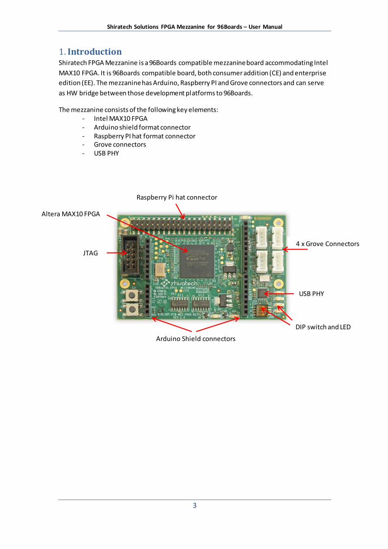
1. Introduction Shiratech FPGA Mezzanine is a 96Boards compatible mezzanine board accommodating Intel
MAX10 FPGA. It is 96Boards compatible board, both consumer addition (CE) and enterprise
edition (EE). The mezzanine has Arduino, Raspberry PI and Grove connectors and can serve
as HW bridge between those development platforms to 96Boards.
The mezzanine consists of the following key elements: - Intel MAX10 FPGA - Arduino shield format connector - Raspberry PI hat format connector - Grove connectors - USB PHY
4 x Grove Connectors
Altera MAX10 FPGA
Arduino Shield connectors
JTAG
USB PHY
DIP switch and LED
Raspberry Pi hat connector
Shiratech Solutions FPGA Mezzanine for 96Boards – User Manual
4
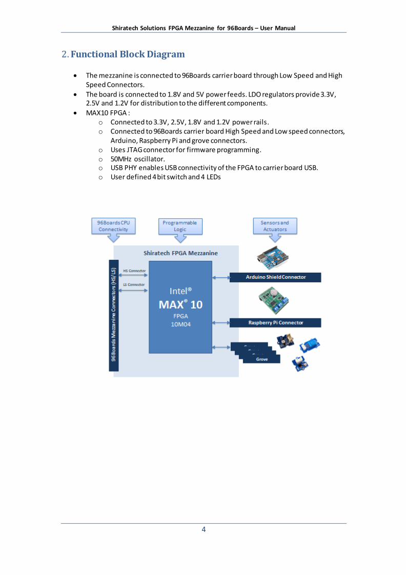
2. Functional Block Diagram
The mezzanine is connected to 96Boards carrier board through Low Speed and High Speed Connectors.
The board is connected to 1.8V and 5V power feeds. LDO regulators provide 3.3V, 2.5V and 1.2V for distribution to the different components.
MAX10 FPGA : o Connected to 3.3V, 2.5V, 1.8V and 1.2V power rails. o Connected to 96Boards carrier board High Speed and Low speed connectors,
Arduino, Raspberry Pi and grove connectors. o Uses JTAG connector for firmware programming. o 50MHz oscillator. o USB PHY enables USB connectivity of the FPGA to carrier board USB. o User defined 4 bit switch and 4 LEDs

Shiratech Solutions FPGA Mezzanine for 96Boards – User Manual
5
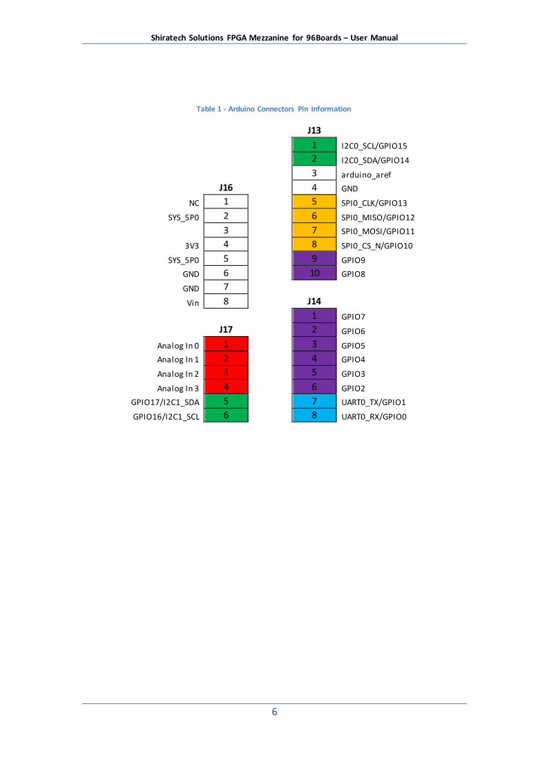
3. Arduino Connectors Pin Information
Connectors J13, J14, J16 and J17 on top of the mezzanine are compatible with Arduino shield
connector format, and the FPGA demo code provided by Shiratech implements a complete
bridge between Arduino and 96Boards connectors.
Upon power up or reset event all pins are configured as input pins to avoid electrical
contention between a connected shield to the FPGA IO pins. To start using the shield the
user should configure the needed GPIO pins using internal registers accessible through I2C0
bus.
Pin configuration options:
1. Each GPIO pin (GPIO2-GPIO9) can be configured as Input or Output pin.
Pins configured as Input pins can be read from a read only register.
Pins configured as Output pins can be read/write from read/write register.
2. I2C, SPI and UART pins can be configured as GPIO or to their specific functionality.
Pins configured as Input pins can be read from a read only register.
Pins configured as Output pins can be read/write from read/write register.
3. If assigned to specific functionality the buses are connected as follows (See table
below):
A. J13 pins 1-2 connected to 96Boards I2C0.
B. J17 pins 5-6 connected to 96Boards I2C1.
C. J13 pins 5-8 connected to 96Boards SPI0.
D. J14 pins 7-8 connected to 96Boards UART0.
For detailed registers description refer to chapter 6 – Control Registers
Attention: The mezzanine supports 3.3V Arduino format shields only. Do not connect 5V
shields as it may damage the FPGA.
Shiratech Solutions FPGA Mezzanine for 96Boards – User Manual
6
Table 1 - Arduino Connectors Pin Information
J13
1 I2C0_SCL/GPIO15
2 I2C0_SDA/GPIO14
3 arduino_aref
J16
4 GND
NC 1
5 SPI0_CLK/GPIO13
SYS_5P0 2
6 SPI0_MISO/GPIO12
3
7 SPI0_MOSI/GPIO11
3V3 4
8 SPI0_CS_N/GPIO10
SYS_5P0 5
9 GPIO9
GND 6
10 GPIO8
GND 7 Vin 8
J14
1 GPIO7
J17
2 GPIO6
Analog In 0 1
3 GPIO5
Analog In 1 2
4 GPIO4
Analog In 2 3
5 GPIO3
Analog In 3 4
6 GPIO2
GPIO17/I2C1_SDA 5
7 UART0_TX/GPIO1
GPIO16/I2C1_SCL 6
8 UART0_RX/GPIO0
Shiratech Solutions FPGA Mezzanine for 96Boards – User Manual
7
4. Raspberry Pi Connector Pin Information
Connector J26 on top of the mezzanine is compatible with Raspberry Pi connector format,
and the FPGA demo code provided by Shiratech implements a complete bridge between
Raspberry Pi and 96Boards connectors.
Upon power up or reset event all pins are configured as input pins to avoid electrical
contention between a connected HAT to the FPGA IO pins. To start using the HAT the user
should configure the needed GPIO pins using internal registers accessible through I2C0 bus.
Pin configuration options:
4. Each GPIO pin can be configured as Input or Output pin.
Pins configured as Input pins can be read from a read only register.
Pins configured as Output pins can be read/write from read/write register.
5. I2C, SPI and UART pins can be configured as GPIO or to their specific functionality.
Pins configured as Input pins can be read from a read only register.
Pins configured as Output pins can be read/write from read/write register.
6. If assigned to specific functionality the buses are connected as follows (See table
below):
E. J26 pins 27-28 are connected to 96Boards I2C0.
F. J26 pins 3 and 5 are connected to 96Boards I2C1.
G. J26 pins 19, 21, 23 and 24 are connected to 96Boards SPI0.
H. J26 pins 26, 35 ,38 and 40 are connected to 96Boards SPI1.
I. J26 pins 8 and 10 are connected to 96Boards UART0.
For detailed registers description refer to chapter 6 – Control Registers
Attention: The mezzanine supports 3.3V HATs only. Do not connect 5V HATs as it may
damage the FPGA.

Shiratech Solutions FPGA Mezzanine for 96Boards – User Manual
8
Table 2 - Raspberry Pi Connector Pin Information
J26
3.3V 1 2 5V
I2C1 SDA 3 4 5V
I2C1 SCL 5 6 GND
GPIO4 7 8 UART TXD
GND 9 10 UART RXD
GPIO17 11 12 GPIO18
GPIO27 13 14 GND
GPIO22 15 16 GPIO23
3.3V 17 18 GPIO24
SPI0 MOSI 19 20 GND
SPI0 MISO 21 22 GPIO25
SPI0 SCLK 23 24 SPI0 CE
GND 25 26 SPI1 CE
I2C0 SDA 27 28 I2C0 SCLK
GPIO5 29 30 GND
GPIO6 31 32 GPIO12
GPIO13 33 34 GND
SPI1 MISO 35 36 GPIO16
GPIO26 37 38 SPI1 MOSI
GND 39 40 SPI1 SCLK

Shiratech Solutions FPGA Mezzanine for 96Boards – User Manual
9
5. Grove Connectors Pin Information TBD
Shiratech Solutions FPGA Mezzanine for 96Boards – User Manual
10
6. Configuration Registers
The firmware provided with the FPGA Mezzanine implements a bridging functionality
between 96Boards to Arduino, Raspberry Pi and Grove.
The design includes I2C slave device with control and configuration register for each of the
IO pins in the expansion connectors.
The I2C device is connected to 96Boards I2C0 bus at address 0x6F.
Device connected to I2C0 Bus.
Device Address:
0x6F
Address: 0x00
Register name: REV_REG
Reset value: 0x10
Access: Read only
MSB
LSB
Bit 7 6 5 4 3 2 1 0
Value 0 0 0 1 0 0 0 0
FPGA firmware revision 1.0
Address: 0x01
Register name: TEST_REG
Reset value: 0x00
Access: Read/Write
MSB
LSB
Bit 7 6 5 4 3 2 1 0
Name T7 T6 T5 T4 T3 T2 T1 T0
Read/write test register.
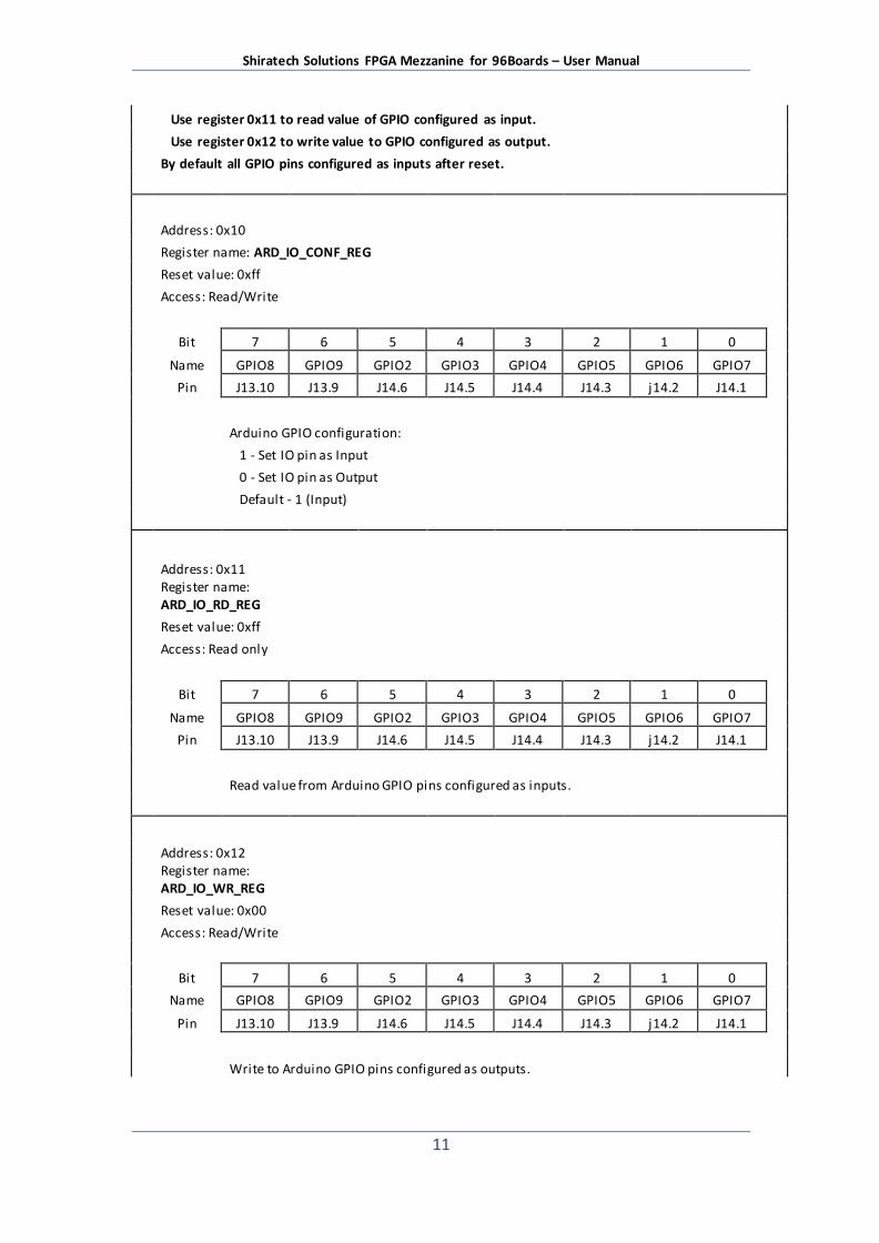
Registers 0x10, 0x11 and 0x12 are used to control Arduino connector GPIO pins:
Use register 0x10 to configure each GPIO as input or output.
Shiratech Solutions FPGA Mezzanine for 96Boards – User Manual
11
Use register 0x11 to read value of GPIO configured as input.
Use register 0x12 to write value to GPIO configured as output.
By default all GPIO pins configured as inputs after reset.
Address: 0x10
Register name: ARD_IO_CONF_REG
Reset value: 0xff
Access: Read/Write
Bit 7 6 5 4 3 2 1 0
Name GPIO8 GPIO9 GPIO2 GPIO3 GPIO4 GPIO5 GPIO6 GPIO7
Pin J13.10 J13.9 J14.6 J14.5 J14.4 J14.3 j14.2 J14.1
Arduino GPIO configuration:
1 - Set IO pin as Input
0 - Set IO pin as Output
Default - 1 (Input)
Address: 0x11
Register name: ARD_IO_RD_REG
Reset value: 0xff
Access: Read only
Bit 7 6 5 4 3 2 1 0
Name GPIO8 GPIO9 GPIO2 GPIO3 GPIO4 GPIO5 GPIO6 GPIO7
Pin J13.10 J13.9 J14.6 J14.5 J14.4 J14.3 j14.2 J14.1
Read value from Arduino GPIO pins configured as inputs.
Address: 0x12
Register name: ARD_IO_WR_REG
Reset value: 0x00
Access: Read/Write
Bit 7 6 5 4 3 2 1 0
Name GPIO8 GPIO9 GPIO2 GPIO3 GPIO4 GPIO5 GPIO6 GPIO7
Pin J13.10 J13.9 J14.6 J14.5 J14.4 J14.3 j14.2 J14.1
Write to Arduino GPIO pins configured as outputs.
Shiratech Solutions FPGA Mezzanine for 96Boards – User Manual
12
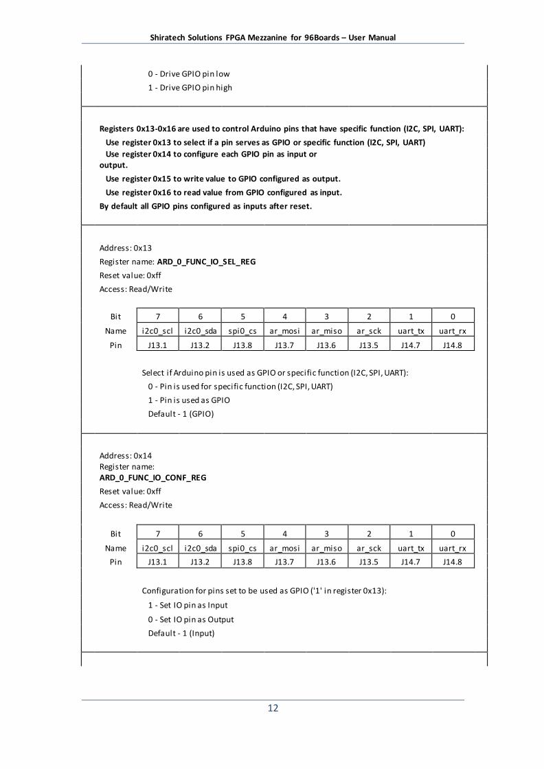
0 - Drive GPIO pin low
1 - Drive GPIO pin high
Registers 0x13-0x16 are used to control Arduino pins that have specific function (I2C, SPI, UART):
Use register 0x13 to select if a pin serves as GPIO or specific function (I2C, SPI, UART)
Use register 0x14 to configure each GPIO pin as input or output.
Use register 0x15 to write value to GPIO configured as output.
Use register 0x16 to read value from GPIO configured as input.
By default all GPIO pins configured as inputs after reset.
Address: 0x13
Register name: ARD_0_FUNC_IO_SEL_REG
Reset value: 0xff
Access: Read/Write
Bit 7 6 5 4 3 2 1 0
Name i2c0_scl i2c0_sda spi0_cs ar_mosi ar_miso ar_sck uart_tx uart_rx
Pin J13.1 J13.2 J13.8 J13.7 J13.6 J13.5 J14.7 J14.8
Select if Arduino pin is used as GPIO or specific function (I2C, SPI, UART):
0 - Pin is used for specific function (I2C, SPI, UART)
1 - Pin is used as GPIO
Default - 1 (GPIO)
Address: 0x14
Register name: ARD_0_FUNC_IO_CONF_REG
Reset value: 0xff
Access: Read/Write
Bit 7 6 5 4 3 2 1 0
Name i2c0_scl i2c0_sda spi0_cs ar_mosi ar_miso ar_sck uart_tx uart_rx
Pin J13.1 J13.2 J13.8 J13.7 J13.6 J13.5 J14.7 J14.8
Configuration for pins set to be used as GPIO ('1' in register 0x13):
1 - Set IO pin as Input
0 - Set IO pin as Output
Default - 1 (Input)

Shiratech Solutions FPGA Mezzanine for 96Boards – User Manual
13
Address: 0x15
Register name: ARD_0_FUNC_IO_WR_REG
Reset value: 0x00
Access: Read/Write
Bit 7 6 5 4 3 2 1 0
Name i2c0_scl i2c0_sda spi0_cs ar_mosi ar_miso ar_sck uart_tx uart_rx
Pin J13.1 J13.2 J13.8 J13.7 J13.6 J13.5 J14.7 J14.8
Write to GPIO pins configured as outputs ('1' in register 0x13 and '0' in register 0x14):
0 - Drive GPIO pin low
1 - Drive GPIO pin high
Address: 0x16
Register name: ARD_0_FUNC_IO_RD_REG
Reset value: 0xff
Access: Read only
Bit 7 6 5 4 3 2 1 0
Name i2c0_scl i2c0_sda spi0_cs ar_mosi ar_miso ar_sck uart_tx uart_rx
Pin J13.1 J13.2 J13.8 J13.7 J13.6 J13.5 J14.7 J14.8
Read from GPIO pins configured as inputs ('1' in register 0x13 and '1' in register 0x14).
Registers 0x17-0x1a are used to control Arduino pins that have specific function (I2C):
Use register 0x17 to select if a pin serves as GPIO or specific function (I2C).
Use register 0x18 to configure each GPIO pin as input or output.
Use register 0x19 to write value to GPIO configured as output.
Use register 0x1a to read value from GPIO configured as input.
By default all GPIO pins configured as inputs after reset.
Address: 0x17
Register name: ARD_1_FUNC_IO_SEL_REG
Reset value: 0xff
Access: Read/Write
Bit 7 6 5 4 3 2 1 0
Name - - - - - - i2c1_scl i2c1_sda
Pin - - - - - - J17.6 J17.5
Shiratech Solutions FPGA Mezzanine for 96Boards – User Manual
14
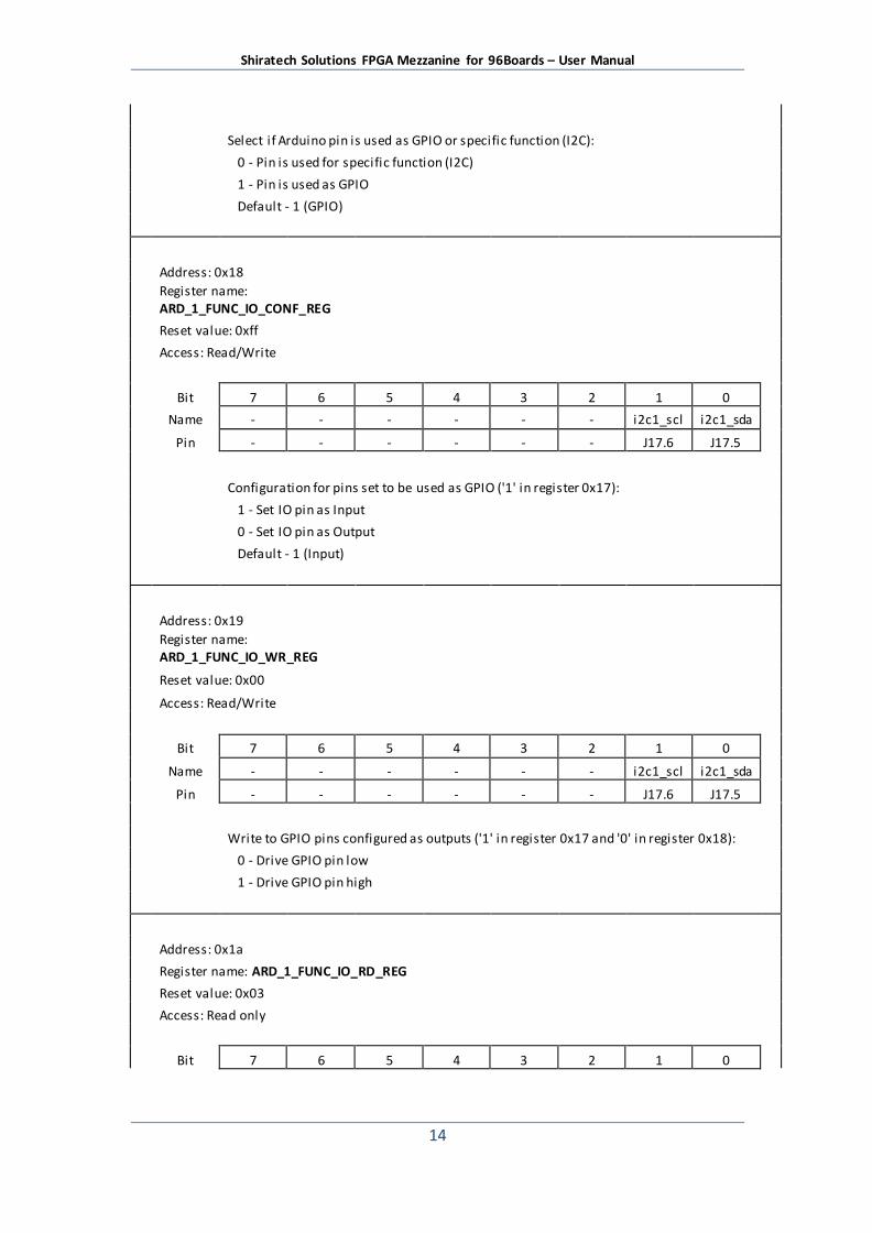
Select if Arduino pin is used as GPIO or specific function (I2C):
0 - Pin is used for specific function (I2C)
1 - Pin is used as GPIO
Default - 1 (GPIO)
Address: 0x18
Register name: ARD_1_FUNC_IO_CONF_REG
Reset value: 0xff
Access: Read/Write
Bit 7 6 5 4 3 2 1 0
Name - - - - - - i2c1_scl i2c1_sda
Pin - - - - - - J17.6 J17.5
Configuration for pins set to be used as GPIO ('1' in register 0x17):
1 - Set IO pin as Input
0 - Set IO pin as Output
Default - 1 (Input)
Address: 0x19
Register name: ARD_1_FUNC_IO_WR_REG
Reset value: 0x00
Access: Read/Write
Bit 7 6 5 4 3 2 1 0
Name - - - - - - i2c1_scl i2c1_sda
Pin - - - - - - J17.6 J17.5
Write to GPIO pins configured as outputs ('1' in register 0x17 and '0' in register 0x18):
0 - Drive GPIO pin low
1 - Drive GPIO pin high
Address: 0x1a
Register name: ARD_1_FUNC_IO_RD_REG
Reset value: 0x03
Access: Read only
Bit 7 6 5 4 3 2 1 0

Shiratech Solutions FPGA Mezzanine for 96Boards – User Manual
15
Name - - - - - - i2c1_scl i2c1_sda
Pin - - - - - - J17.6 J17.5
Read from GPIO pins configured as inputs ('1' in register 0x17 and '1' in register 0x18).
Registers 0x30-0x35 are used to control Raspberry Pi connector GPIO pins:
Use registers 0x30-0x31 to configure each GPIO as input or output.
Use register 0x32-0x33 to read value of GPIO configured as input.
Use register 0x34-0x35 to write value to GPIO configured as output.
By default all GPIO pins configured as inputs after reset.
Address: 0x30
Register name: RPI_IO_CONF_REG_0
Reset value: 0xff
Access: Read/Write
Bit 7 6 5 4 3 2 1 0
Name GPIO4 GPIO24 GPIO23 GPIO22 GPIO27 GPIO17 GPIO6 GPIO5
Pin J26.7 J26.18 J26.16 J26.15 J26.13 J26.11 J26.31 J26.29
Raspberry Pi GPIO configuration:
1 - Set IO pin as Input
0 - Set IO pin as Output
Default - 1 (Input)
Address: 0x31
Register name: RPI_IO_CONF_REG_1
Reset value: 0xff
Access: Read/Write
Bit 7 6 5 4 3 2 1 0
Name - - GPIO18 GPIO25 GPIO12 GPIO16 GPIO26 GPIO13
Pin - - J26.12 J26.22 J26.32 J26.36 J26.37 J26.33
Raspberry Pi GPIO configuration:
1 - Set IO pin as Input
0 - Set IO pin as Output
Default - 1 (Input)
Shiratech Solutions FPGA Mezzanine for 96Boards – User Manual
16
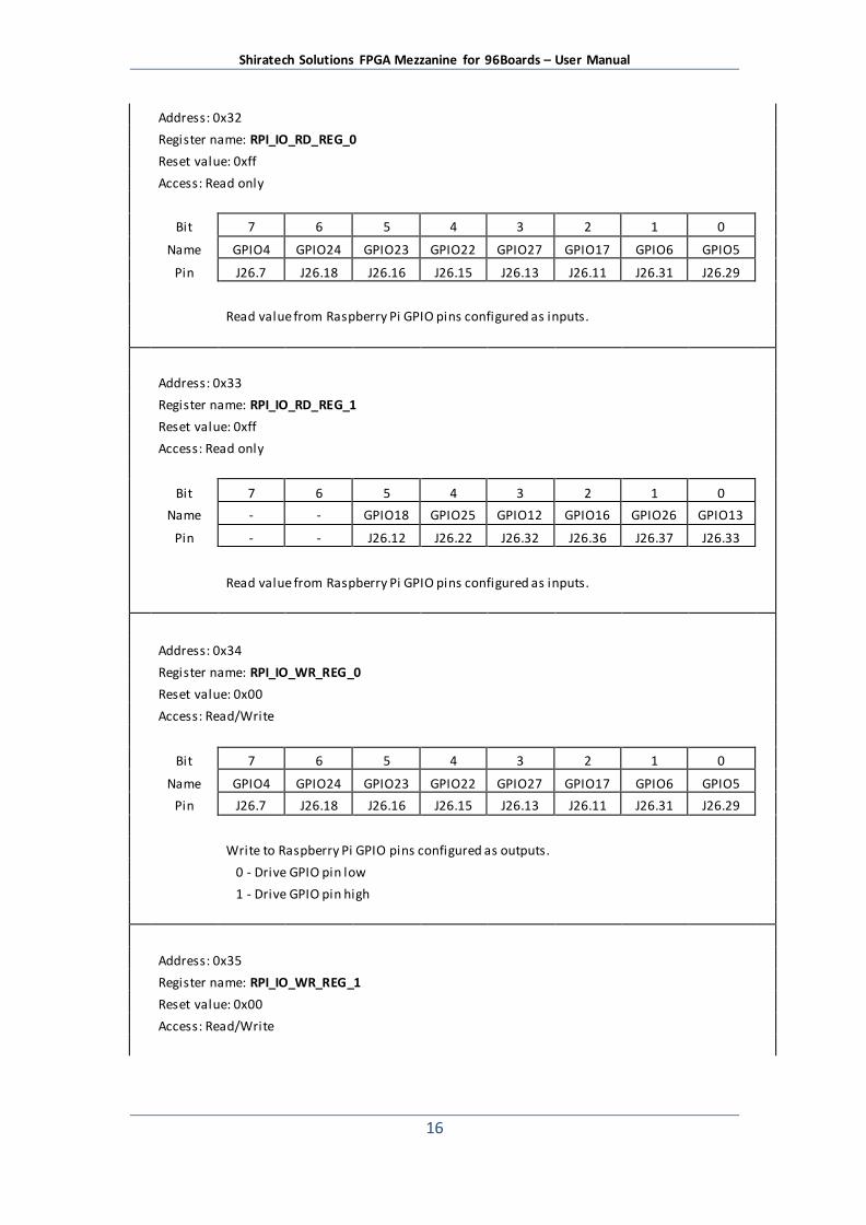
Address: 0x32
Register name: RPI_IO_RD_REG_0
Reset value: 0xff
Access: Read only
Bit 7 6 5 4 3 2 1 0
Name GPIO4 GPIO24 GPIO23 GPIO22 GPIO27 GPIO17 GPIO6 GPIO5
Pin J26.7 J26.18 J26.16 J26.15 J26.13 J26.11 J26.31 J26.29
Read value from Raspberry Pi GPIO pins configured as inputs.
Address: 0x33
Register name: RPI_IO_RD_REG_1
Reset value: 0xff
Access: Read only
Bit 7 6 5 4 3 2 1 0
Name - - GPIO18 GPIO25 GPIO12 GPIO16 GPIO26 GPIO13
Pin - - J26.12 J26.22 J26.32 J26.36 J26.37 J26.33
Read value from Raspberry Pi GPIO pins configured as inputs.
Address: 0x34
Register name: RPI_IO_WR_REG_0
Reset value: 0x00
Access: Read/Write
Bit 7 6 5 4 3 2 1 0
Name GPIO4 GPIO24 GPIO23 GPIO22 GPIO27 GPIO17 GPIO6 GPIO5
Pin J26.7 J26.18 J26.16 J26.15 J26.13 J26.11 J26.31 J26.29
Write to Raspberry Pi GPIO pins configured as outputs.
0 - Drive GPIO pin low
1 - Drive GPIO pin high
Address: 0x35
Register name: RPI_IO_WR_REG_1
Reset value: 0x00
Access: Read/Write

Shiratech Solutions FPGA Mezzanine for 96Boards – User Manual
17
Bit 7 6 5 4 3 2 1 0
Name - - GPIO18 GPIO25 GPIO12 GPIO16 GPIO26 GPIO13
Pin - - J26.12 J26.22 J26.32 J26.36 J26.37 J26.33
Write to Raspberry Pi GPIO pins configured as outputs.
0 - Drive GPIO pin low
1 - Drive GPIO pin high
Registers 0x36-0x39 are used to control RPi pins that have specific function (I2C, SPI, UART):
Use register 0x36 to select if a pin serves as GPIO or specific function (I2C, SPI, UART)
Use register 0x37 to configure each GPIO pin as input or
output.
Use register 0x38 to write value to GPIO configured as output.
Use register 0x39 to read value from GPIO configured as input.
By default all GPIO pins configured as inputs after reset.
Address: 0x36
Register name: RPI_0_FUNC_IO_SEL_REG
Reset value: 0xff
Access: Read/Write
Bit 7 6 5 4 3 2 1 0
Name - - SP1 CE SPI1
MOSI SPI1
MISO SPI1 SCLK
UART TXD
UART RXD
Pin - - J26.26 J26.38 J26.35 J26.40 J26.8 J26.10
Select if RPi pin is used as GPIO or specific function (I2C, SPI, UART):
0 - Pin is used for specific function (I2C, SPI, UART)
1 - Pin is used as GPIO
Default - 1 (GPIO)
Address: 0x37
Register name:
RPI_0_FUNC_IO_CONF_REG
Reset value: 0xff
Access: Read/Write
Bit 7 6 5 4 3 2 1 0
Name - - SP1 CE
SPI1
MOSI
SPI1
MISO
SPI1
SCLK
UART
TXD
UART
RXD
Pin - - J26.26 J26.38 J26.35 J26.40 J26.8 J26.10

Shiratech Solutions FPGA Mezzanine for 96Boards – User Manual
18
Configuration for pins set to be used as GPIO ('1' in register 0x36):
1 - Set IO pin as Input
0 - Set IO pin as Output
Default - 1 (Input)
Address: 0x38
Register name: RPI_0_FUNC_IO_WR_REG
Reset value: 0x00
Access: Read/Write
Bit 7 6 5 4 3 2 1 0
Name - - SP1 CE SPI1
MOSI SPI1
MISO SPI1 SCLK
UART TXD
UART RXD
Pin - - J26.26 J26.38 J26.35 J26.40 J26.8 J26.10
Write to GPIO pins configured as outputs ('1' in register 0x36 and '0' in register 0x37):
0 - Drive GPIO pin low
1 - Drive GPIO pin high
Address: 0x39
Register name: RPI_0_FUNC_IO_RD_REG
Reset value: 0x3f
Access: Read only
Bit 7 6 5 4 3 2 1 0
Name - - SP1 CE SPI1
MOSI SPI1
MISO SPI1 SCLK
UART TXD
UART RXD
Pin - - J26.26 J26.38 J26.35 J26.40 J26.8 J26.10
Read from GPIO pins configured as inputs ('1' in register 0x36 and '1' in register 0x37).
Registers 0x3a-0x3d are used to control RPi pins that have specific function (I2C, SPI, UART):
Use register 0x3a to select if a pin serves as GPIO or specific function (I2C, SPI, UART)
Use register 0x3b to configure each GPIO pin as input or
output.
Use register 0x3c to write value to GPIO configured as output.
Use register 0x3d to read value from GPIO configured as input.
By default all GPIO pins configured as inputs after reset.
Address: 0x3a

Shiratech Solutions FPGA Mezzanine for 96Boards – User Manual
19
Register name: RPI_1_FUNC_IO_SEL_REG
Reset value: 0xff
Access: Read/Write
Bit 7 6 5 4 3 2 1 0
Name I2C1 SCL
I2C1
SDA
I2C0
SCLK
I2C0
SDA SPI0 CE
SPI0
MOSI
SPI0
MISO
SPI0
SCLK
Pin J26.5 J26.3 J26.28 J26.27 J26.24 J26.19 J26.21 J26.23
Select if RPi pin is used as GPIO or specific function (I2C, SPI, UART):
0 - Pin is used for specific function (I2C, SPI, UART)
1 - Pin is used as GPIO
Default - 1 (GPIO)
Address: 0x3b
Register name: RPI_1_FUNC_IO_CONF_REG
Reset value: 0xff
Access: Read/Write
Bit 7 6 5 4 3 2 1 0
Name I2C1 SCL I2C1 SDA
I2C0 SCLK
I2C0 SDA SPI0 CE
SPI0 MOSI
SPI0 MISO
SPI0 SCLK
Pin J26.5 J26.3 J26.28 J26.27 J26.24 J26.19 J26.21 J26.23
Configuration for pins set to be used as GPIO ('1' in register 0x3a):
1 - Set IO pin as Input
0 - Set IO pin as Output
Default - 1 (Input)
Address: 0x3c
Register name: RPI_1_FUNC_IO_WR_REG
Reset value: 0x00
Access: Read/Write
Bit 7 6 5 4 3 2 1 0
Name I2C1 SCL I2C1 SDA
I2C0 SCLK
I2C0 SDA SPI0 CE
SPI0 MOSI
SPI0 MISO
SPI0 SCLK
Pin J26.5 J26.3 J26.28 J26.27 J26.24 J26.19 J26.21 J26.23
Write to GPIO pins configured as outputs ('1' in register 0x3a and '0' in register 0x3b):
0 - Drive GPIO pin low
1 - Drive GPIO pin high

Shiratech Solutions FPGA Mezzanine for 96Boards – User Manual
20
Address: 0x3d
Register name: RPI_1_FUNC_IO_RD_REG
Reset value: 0xff
Access: Read only
Bit 7 6 5 4 3 2 1 0
Name I2C1 SCL I2C1 SDA
I2C0 SCLK
I2C0 SDA SPI0 CE
SPI0 MOSI
SPI0 MISO
SPI0 SCLK
Pin J26.5 J26.3 J26.28 J26.27 J26.24 J26.19 J26.21 J26.23
Read from GPIO pins configured as inputs ('1' in register 0x3a and '1' in register 0x3b).
Address: 0xa0
Register name: LED_REG
Reset value: 0x00
Access: Read/Write
MSB
LSB
Bit 7 6 5 4 3 2 1 0
Name - - - - LED3 LED2 LED1 LED0
Turn user LED on/off:
0 - LED off
1 - LED on
Address: 0xa1
Register name: SWITCH_REG
Reset value: 0x00
Access: Read only
MSB
LSB
Bit 7 6 5 4 3 2 1 0
Name - - - - SW3 SW2 SW1 SW0
Read user DIP switch value.
Shiratech Solutions FPGA Mezzanine for 96Boards – User Manual
21
7. Document Revision History
Revision Date Author Status and Description
0.9 20/12/2018 Guy Zohar Initial version
Top Related