


Languages
Pages
Legal

Published SFF-8431, Revision 4.1
SFF Committee documentation may be purchased in hard copy or electronic form.
SFF specifications are available at ftp://ftp.seagate.com/sff
SFF Committee
SFF-8431 Specifications for
Enhanced Small Form Factor Pluggable Module SFP+
Revision 4.1
6th of July 2009
Secretariat: SFF Committee
Abstract: This document defines the low speed electrical and management interface specifications for enhanced Small Form
Factor Pluggable (SFP+) modules and hosts. The SFP+ module is a hot pluggable small footprint serial-to-serial data-agnostic
optical transceiver. This document defines the high speed electrical interface specifications for 10 Gigabit/s SFP+ modules
and hosts. The 8.5 Gigabit/s high speed electrical interface specifications are defined in FC-PI-4. The modules may optionally
support lower signalling rates as well. The modules may be used to implement single-mode or multimode serial optical inter-
faces at 850 nm, 1310 nm, or 1550 nm. The SFP+ module design may use one of several different optical connectors.
This specification provides a common reference for system manufacturers, system integrators, and suppliers. This is an inter-nal working specification of the SFF Committee, an industry ad hoc group.
This specification is made available for public review, and written comments are solicited from readers. Comments received by the members will be considered for inclusion in future revisions of this specification.
Support: This specification is supported by the identified member companies of the SFF Committee.
POINTS OF CONTACT:
Technical Editor: Chairman SFF Committee
Ali Ghiasi I. Dal Allan
Broadcom Corporation ENDL
3151 Zanker Road 14426 Black Walnut Court
San Jose, CA 95134 Saratoga, CA 95070
Voice: (408) 922-7423 Voice: (408) 867-6630
EMail: [email protected] EMail: [email protected]
SSWG Leader:
Tom Lindsay
ClariPhy Communications
16 Technology Drive, Suite 165
Irvine, CA 92618
Voice: (425)608-0209
EMail: [email protected]
SFP+ (Enhanced 10 Gbps pluggable module)

Published SFF-8431, Revision 4.1
EXPRESSION OF SUPPORT BY MANUFACTURERS
The following member companies of the SFF Committee voted in favor of this industry specification:
AMCC Amphenol Arista Networks Avago Broadcom Cinch Clariphy Cortina Systems EMC Emulex ETRI Finisar Foxconn Fujitsu CPA Hewlett Packard Hitachi GST JDS Uniphase Luxtera Molex NetLogic uSyst OpNext Panduit Picolight QLogic Samsung Sumitomo Sun Microsystems Tyco Vitesse Semiconductor W L Gore
The following member companies of the SFF Committee voted to abstain on this industry specification.
Comax FCI ICT Solutions Leoni Cables Meritec Seagate Toshiba
The user's attention is called to the possibility that implementation to this Specification may require use of an invention cov-ered by patent rights. By distribution of this specification, no position is taken with respect to the validity of a claim or claims of any patent rights in connection therewith. Members of the SFF Committee which advise that a patent exists are required to provide a statement of willingness to grant a license under these rights on reasonable and non-discriminatory terms and conditions to applicants desiring to obtain such a license.
SFP+ (Enhanced 10 Gbps Pluggable Module)) Page ii
Published SFF-8431, Revision 4.1
Foreword
The development work on this specification was done by the SFF Committee, an industry group. The membership of the committee since its formation in August 1990 has included a mix of companies which are leaders across the industry.
When 2 1/2” diameter disk drives were introduced, there was no commonality on external dimensions e.g. physical size, mounting locations, connector type, connector location, between vendors.
The first use of these disk drives was in specific applications such as laptop portable computers and system integrators worked individually with vendors to develop the packaging. The result was wide diversity, and incompatibility.
The problems faced by integrators, device suppliers, and component suppliers led to the formation of the SFF Committee as an industry ad hoc group to address the marketing and engineering considerations of the emerging new technology.
During the development of the form factor definitions, other activities were suggested because participants in the SFF Com-mittee faced more problems than the physical form factors of disk drives. In November 1992, the charter was expanded to address any issues of general interest and concern to the storage industry. The SFF Committee became a forum for resolving industry issues that are either not addressed by the standards process or need an immediate solution.
Those companies which have agreed to support a specification are identified in the first pages of each SFF Specification. Industry consensus is not an essential requirement to publish an SFF Specification because it is recognized that in an emerg-ing product area, there is room for more than one approach. By making the documentation on competing proposals avail-able, an integrator can examine the alternatives available and select the product that is felt to be most suitable.
SFF Committee meetings are held during T10 weeks (see www.t10.org), and Specific Subject Working Groups are held at the convenience of the participants. Material presented at SFF Committee meetings becomes public domain, and there are no restrictions on the open mailing of material presented at committee meetings.
Most of the specifications developed by the SFF Committee have either been incorporated into standards or adopted as standards by EIA (Electronic Industries Association), ANSI (American National Standards Institute) and IEC (International Elec-trotechnical Commission).
The SFF Committee activities support the requirements of the storage industry, and it is involved with several standards.
If you are interested in participating or wish to follow the activities of the SFF Committee, the signup for membership and/or documentation can be found at:
www.sffcommittee.com/ie/join.html
The complete list of SFF Specifications which have been completed or are currently being worked on by the SFF Committee can be found at:
ftp://ftp.seagate.com/sff/SFF-8000.TXT
If you wish to know more about the SFF Committee, the principles which guide the activities can be found at:
ftp://ftp.seagate.com/sff/SFF-8032.TXT
Suggestions for improvement of this specification will be welcome. They should be sent to the SFF Committee, 14426 Black Walnut Ct, Saratoga, CA 95070.
SFP+ (Enhanced 10 Gbps Pluggable Module)) Page iii

Published SFF-8431, Revision 4.1
Industry Documents
The following interface standards are relevant to SFP+ Specifications. SFF-8432 - Improved Pluggable Formfactor (ftp://ftp.seagate.com/sff/)SFF-8083 - Improved 0.8mm Card Edge Connector (ftp://ftp.seagate.com/sff/)SFF-8089 - SFP Rate and Application codes (ftp://ftp.seagate.com/sff/)SFF-8079 - SFP Rate and Application Selection (ftp://ftp.seagate.com/sff/)SFF-8472 - Diagnostic Monitoring Interface for Optical Transceivers (ftp://ftp.seagate.com/sff/)INF-8074i - SFP (Small Form Factor) Transceiver (ftp://ftp.seagate.com/sff/)INF-8077i - 10 Gigabit Small Form Factor Pluggable Module (XFP MSA) (ftp://ftp.seagate.com/sff/)FC-PI-4 - Fibre Channel - Physical Interface-410GFC - Fibre Channel - 10 GigabitFC-MJSQ - Methodologies for Jitter and Signal Quality Specifications FC INCITS Project 1316-DT Rev 14.1, June 5, 2005IEEE 802.3 - IEEE Standard 802.3, Relevant 10 Gigabit Ethernet clauses are 49, 10GBASE-R LAN PHY; 50, 10GBASE-W WAN PHY; 52, 10 Gigabit Ethernet serial PMDs; and 68, 10GBASE-LRM)OIF CEI - Optical Internetworking Forum - Implementation Agreement # OIF-CEI-02.0 Common Electrical I/O (CEI) (http://www.oiforum.com/public/impagreements.html)
Acronyms and other abbreviations
64B/66B Data encoded with 64B/66B encoder as defined by the IEEE Std. 802.3 CL 49.
BER bit error ratio
CDR clock and data recovery
CRU clock recovery unit
dBdecibel. 10*log10(ratio of power quantities). Powers can be electrical or optical. Conventional usage. See also dBe and
dBo.
dBeSpecific case of dB where signals are electrical. 10*log10(ratio of electrical power quantities). 20*log10(ratio of voltage
quantities) can be used if reference impedances are equal.
dBm decibel (relative to 1 mW)
dBo
Specific case of dB where the signals are in optical power. 10*log10(ratio of optical power quantities). Also, in certain
cases with electrical signals relating to linear optical modules, where it is expected that electrical voltage is in proportion
to optical power, 10*log10(ratio of voltage quantities).
DCD Duty cycle distortion
DDPWS Data Dependent Pulse Width Shrinkage
DDJ Data Dependent Jitter
dRN Difference of Relative noise see Appendix D
DUT device under test
dWDP Difference of the waveform distortion penalty of an optical receiver
dWDPc Difference of the waveform distortion penalty of an electrical cable assembly
EMC electromagnetic compatibility
EMI electromagnetic Interference
FC Fibre Channel
h hexadecimal notation
HCB Host Compliance Board
IEEE Institute of Electrical and Electronics Engineers
ITU-T ITU Telecommunication Standardization Sector
Gbit gigabit = 109 bits
GBd Gigabaud
J2 99% Jitter
LRMIEEE 802.3 CL68 Physical Layer Specifications for 10Gb/s using 10GBASE-R encoding and long wavelength optics for
multimode fiber
SFP+ (Enhanced 10 Gbps Pluggable Module)) Page iv

Published SFF-8431, Revision 4.1
SFF Specifications
There are several projects active within the SFF Committee. The complete list of specifications which have been completed or are still being worked on are listed in the specification at ftp://ftp.seagate.com/sff/SFF-8000.TXT
Document Sources
Those who join the SFF Committee as an Observer or Member receive electronic copies of the minutes and SFF specifications (http://www.sffcommittee.com/ie/join.html).
Copies of ANSI standards may be purchased from the InterNational Committee for Information Technology Standards (http://tinyurl.com/c4psg).
Copies of SFF, T10 (SCSI), T11 (Fibre Channel) and T13 (ATA) standards and standards still in development are available on the HPE version of CD_Access (http://tinyurl.com/85fts).
MCB Module Compliance Board
OMA optical modulation amplitude
PCB printed circuit board
PRBS9 Pseudo-Random Bit Sequence 29-1, see D.1.1
PRBS31 Pseudo-Random Bit Sequence 231-1, see D.1.1
Qsq Qsq a measure of SNR, see D.8 and IEEE 802.3.68.6.7
RI random interference
RMS root mean square
RN relative noise
Rx receiver
Rx_LOS Loss of signal same as defined in FC PI-4 and the inverse of signal detect (SD) in 802.3
RSS “Root Sum of Squares”
SD Signal Detect
SerDes Serializer/Deserializer
SFI SFP+ high speed serial electrical interface
SNR signal-to-noise ratio
VccT Module positive power supply rail for the transmitter
VccR Module positive power supply rail for the receiver
VMA voltage modulation amplitude
Tx transmitter
TWDP Transmitter Waveform Distortion Penalty for an optical transmitter
TWDPc Transmitter Waveform Distortion Penalty of a host transmitter supporting an electrical cable assembly
UI unit interval = 1 symbol period
UJ Uncorrelated Jitter
WDP Waveform distortion penalty
WDPc Waveform distortion penalty for an electrical cable assembly
SFP+ (Enhanced 10 Gbps Pluggable Module)) Page v

Published SFF-8431, Revision 4.1
Conventions
The American convention of numbering is used i.e., the thousands and higher multiples are separated by a comma and a period is used as the decimal point. This is equivalent to the ISO/IEC convention of a space and comma.
American: ISO:0.6 0,61,000 1 000 1,323,462.9 1 323 462,9
SFP+ Publication History
Revision Number
Description Date
0.1 Initial Publication of Document, Preliminary May 9, 2006
0.5 Initial Public Review Draft June 29, 2006,
1.0 2nd Public Draft August 28, 2006
1.1 3rd Public Draft October 10, 2006
1.2 4rd Public Draft December 21, 2006
1.3 5rd Public Draft February 16, 2007
2.0 6th Public Draft and the 1st SFF A ballot April 26, 2007
2.1 7th Public Draft August 30, 2007
2.2 8th Public Draft December 19, 2007
3.0 9th Public Draft and the 2nd SFF A ballot May 8, 2008
3.1 Editor review draft November 11, 2008
3.2 10th Public Draft and the 3rd SFF A ballot November 12, 2008
3.3 11th Public Draft and the 4rd SFF A ballot April 8, 2009
4.0 12th Public Draft and the 1st SFF Publication Ballot
Valid comments were made on draft revision 3.3 that mask hit ratios of 1e-12 at C’ and C” compliance points are too time consuming for normal testing. While changes to the document to enable extrapolation from 1e-12 to a higher hit ratio would be desirable, due to concerns that developing a better specification would delay the schedule, no so-lutions are provided in this revision of SFF-8431. Improved testing methods should be considered for future projects.
June 11, 2009
4.1 Published
It was proposed to truncate the diamond mask into a hexagonal mask while maintaining the current slope of the diamond mask. The underlying reason for this comment was that the downstream CDR due to setup and hold times could not use the upper and low-er apexes of the diamond mask. It was considered with interest but it could not be ac-commodated with the schedule.
July 6, 2009
SFP+ (Enhanced 10 Gbps Pluggable Module)) Page vi

Published SFF-8431, Revision 4.1
Contents
Chapter 1 Scope of SFP+ Specification ................................................................................. 1
1.1 Introduction ............................................................................................................................................................................. 1
1.2 The SFP+ Supported Standards ........................................................................................................................................ 2
1.3 SFI Typical PCB Reach (Informative)................................................................................................................................. 3
Chapter 2 Low Speed Electrical and Power Specifications .................................................. 4
2.1 Introduction ............................................................................................................................................................................. 4
2.2 General Requirements .......................................................................................................................................................... 4
2.3 SFP+ Host Connector Definition....................................................................................................................................... 4
2.4 Low Speed Electrical Control Contacts and 2-wire Interface.................................................................................. 7
2.4.1 Tx_Fault ....................................................................................................................................................................................7
2.4.2 Tx_Disable ...............................................................................................................................................................................7
2.4.3 RS0/RS1 ....................................................................................................................................................................................7
2.4.4 Mod_ABS .................................................................................................................................................................................8
2.4.5 SCL/SDA ...................................................................................................................................................................................8
2.4.6 Rx_LOS......................................................................................................................................................................................8
2.5 Rate Select Hardware Control ............................................................................................................................................ 8
2.6 Low Speed Electrical Specifications................................................................................................................................. 9
2.6.1 Module Low Speed Electrical Specifications ..............................................................................................................9
2.6.2 Host Low speed Electrical Specifications.................................................................................................................. 10
2.7 Timing Requirement of Control and Status I/O .........................................................................................................11
2.7.1 Module power on initialization procedure, Tx_Disable negated.................................................................... 12
2.7.2 Module power on initialization procedure, Tx_Disable asserted. .................................................................... 12
2.7.3 Initialization During Hot Plugging .............................................................................................................................. 13
2.7.4 Transmitter management............................................................................................................................................... 14
2.7.5 Transmitter safety detection and presentation ...................................................................................................... 14
2.7.6 Module fault recovery...................................................................................................................................................... 15
2.7.7 Module loss of signal indication................................................................................................................................... 16
2.8 SFP+ Power Requirement..................................................................................................................................................17
2.8.1 Module Power Supply Requirements......................................................................................................................... 17
2.8.2 Host Power Supply Noise Output ................................................................................................................................ 17
2.8.3 Module Power Supply Noise Output.......................................................................................................................... 17
2.8.4 Power Supply Noise Tolerance...................................................................................................................................... 17
2.9 ESD ........................................................................................................................................................................19
SFP+ (Enhanced 10 Gbps pluggable module) Page vii

Published SFF-8431, Revision 4.1
Chapter 3 High Speed Electrical Specification SFI ............................................................. 20
3.1 Introduction ...........................................................................................................................................................................20
3.2 SFI Applications Definition................................................................................................................................................20
3.3 SFI Test Points Definition and Measurements............................................................................................................21
3.3.1 Host Compliance Points .................................................................................................................................................. 21
3.3.2 Module Compliance Points ............................................................................................................................................ 22
3.3.3 ASIC/SerDes Test Points (Informative)........................................................................................................................ 23
3.3.4 Host Input Calibration Point .......................................................................................................................................... 24
3.3.5 Module Input Calibration Point .................................................................................................................................... 24
3.4 SFI Termination and DC Blocking ...................................................................................................................................25
3.5 SFP+ Host System Specifications....................................................................................................................................27
3.5.1 Host Transmitter Output Specifications at B............................................................................................................ 27
3.5.2 Host Receiver Input Specifications at C and C”....................................................................................................... 30
3.6 SFP+ Module Specifications .............................................................................................................................................35
3.6.1 Module Transmitter Input Specifications at B’ and B”.......................................................................................... 35
3.6.2 Module Receiver Output Specifications at C’ .......................................................................................................... 37
Chapter 4 SFP+ 2-wire Interface .......................................................................................... 41
4.1 Introduction ...........................................................................................................................................................................41
4.2 2-wire Electrical Specifications ........................................................................................................................................41
4.3 SFP+ 2-wire Timing Diagram............................................................................................................................................42
4.4 Memory Transaction Timing ............................................................................................................................................43
4.5 Device Addressing and Operation .................................................................................................................................44
4.6 Read/Write Functionality ...................................................................................................................................................45
4.6.1 SFP+ Memory Address Counter (Read and Write Operations).......................................................................... 45
4.6.2 Read Operations (Current Address Read) ................................................................................................................. 46
4.6.3 Read Operations (Random Read)................................................................................................................................. 46
4.6.4 Read Operations (Sequential Read) ............................................................................................................................ 47
4.6.5 Write Operations (Byte Write) ....................................................................................................................................... 48
4.6.6 Write Operations (Sequential Write)........................................................................................................................... 49
4.6.7 Write Operations (Acknowledge Polling).................................................................................................................. 49
Appendix A SFI Channel Recommendation (Informative) ................................................... 50
A.1 SFI Host Channel General Recommendations...........................................................................................50
A.2 SFI Channel Transfer Recommendations.....................................................................................................50
A.3 SFI Channel Return Loss Recommendations .............................................................................................52
A.4 SFI Channel Ripple Recommendations........................................................................................................52
Appendix B SFI ASIC/SerDes Specification (Informative) .................................................... 54
B.1 Introduction...........................................................................................................................................................54
B.2 SFI ASIC/SerDes Transmitter Output Specifications at A (Informative) ............................................54
SFP+ (Enhanced 10 Gbps pluggable module) Page viii

Published SFF-8431, Revision 4.1
B.3 SFI ASIC/SerDes Receiver Input Specifications at D (Informative) .....................................................54
Appendix C Application Reference Boards (Normative) ........ ............................................. 56
C.1 Compliance Boards .............................................................................................................................................56
C.1.1 Host Compliance Board Transfer Characteristics.......................................................................56
C.1.2 Module Compliance Board Transfer Characteristics ................................................................57
C.1.3 ASIC/SerDes Test Board Transfer Characteristics .......................................................................58
C.2 Host Compliance Board.....................................................................................................................................59
C.2.1 Host Compliance Board Material and Layer Stack-up .............................................................59
C.2.2 Host Compliance Board Partlist .......................................................................................................60
C.2.3 HCB Gerber Files....................................................................................................................................60
C.2.4 Schematic of Host Compliance Board...........................................................................................60
C.3 Module Compliance Board...............................................................................................................................62
C.3.1 Module Compliance Board Material and Layer Stack-up .......................................................62
C.3.2 Schematic of Module Compliance Board.....................................................................................63
C.3.3 Module Compliance Board Partlist.................................................................................................65
C.3.4 MCB Gerber files....................................................................................................................................65
C.4 Specifications for Mated Host and Module Compliance Boards ........................................................66
Appendix D Test Methodology and Measurement (Normative) ......................................... 72
D.1 Introduction...........................................................................................................................................................72
D.1.1 Test Patterns............................................................................................................................................72
D.2 Eye Mask Compliance.........................................................................................................................................72
D.2.1 Example Calculations for 5x10⁻⁵ Hit Ratio...................................................................................73
D.3 Data Dependent Jitter (DDJ) and Pulse Width Shrinkage (DDPWS) .................................................74
D.3.1 Duty Cycle Distortion (DCD) .............................................................................................................75
D.4 Uncorrelated Jitter (UJ) ......................................................................................................................................75
D.5 99% Jitter (J2) and Total Jitter (TJ) .................................................................................................................76
D.6 Rise and Fall Times...............................................................................................................................................77
D.7 Voltage Modulation Amplitude (VMA) ........................................................................................................77
D.8 Relative Noise (RN) ..............................................................................................................................................78
D.9 Waveform Distortion Penalty (WDP).............................................................................................................79
D.10 Electrical compliance signal at B” for the SFP+ Module transmitter .................................................80
D.11 Test Method for a host receiver for a limiting module ...........................................................................82
D.11.1 Test Equipment & Setup .....................................................................................................................83
D.11.2 Stressed-Eye Jitter Characteristics ..................................................................................................83
D.11.3 Calibration ...............................................................................................................................................85
D.11.4 Calibration Procedure..........................................................................................................................86
D.11.5 Test Procedure........................................................................................................................................87
D.12 Limiting Module Receiver Compliance Tests .............................................................................................87
D.13 Test Method for a Host Receiver with a Linear Module..........................................................................88
SFP+ (Enhanced 10 Gbps pluggable module) Page ix

Published SFF-8431, Revision 4.1
D.13.1 Test Description and Procedure for Host Receiver for Linear Module ...........................89
D.13.2 Host Linear Tester calibration.......................................................................................................90
D.14 Linear Module Receiver Compliance Tests .............................................................................................91
D.14.1 Linear Module receiver noise compliance test.......................................................................91
D.14.2 linear Module Receiver Distortion Penalty Compliance Test ............................................93
D.14.3 Linear Module Receiver Output Differential Peak-Peak Voltage .....................................94
D.15 AC Common Mode Voltage..........................................................................................................................95
D.15.1 Definition of AC Common Mode Voltage ................................................................................95
D.15.2 AC Common Mode Generation Test ..........................................................................................95
D.15.3 AC Common Mode Tolerance Test..............................................................................................95
D.16 Termination Mismatch ..................................................................................................................................95
D.17 Power Supply Testing methodology.........................................................................................................96
D.17.1 Host Power Supply Noise Output ...............................................................................................97
D.17.2 SFP+ Module Power Supply Noise Output..............................................................................99
D.17.3 Module Power Supply Tolerance Testing .................................................................................99
Appendix E SFP+ Direct Attach Cable Specifications “10GSFP+Cu” (Optional) ........... 101
E.1 10GSFP+Cu Direct Attach Construction............................................................................................... 101
E.2 SFP+ Host Output Specifications for Passive Direct Attach Cables ............................................ 102
E.2.1 Transmitter Stressor ...................................................................................................................... 102
E.3 SFP+ Host Receiver Supporting 10GSFP+Cu Input Compliance Test Signal Calibrated at C”104
E.3.1 Copper Host Receiver Specifications ...................................................................................... 104
E.3.2 Copper Host Stress Generator 1 UI Pulse Response .......................................................... 105
E.4 SFP+ Passive Direct Attach cable Assembly Specifications ........................................................... 107
E.4.1 SFP+ Direct Attach Cable Test Setup ...................................................................................... 108
E.4.2 Cable dWDP Test Procedure....................................................................................................... 109
E.4.3 Cable NEXT Measurement Procedure..................................................................................... 109
E.4.4 VMA to Crosstalk Ratio (VCR)..................................................................................................... 110
Appendix F 1.25 GBd Operation Support (Optional) ............. ........................................ 112
F.1 Introduction.................................................................................................................................................... 112
F.2 SFP+ Host Operation Guideline for Supporting Classic SFP ......................................................... 112
Appendix G Matlab Code for TWDP ......................................... ........................................ 115
SFP+ (Enhanced 10 Gbps pluggable module) Page x
Published SFF-8431, Revision 4.1
List of Tables
Table 1 SFP+ Standard Compliance .......................................................................................................... 2
Table 2 Host Board Achievable Trace Length .......................................................................................... 3
Table 3 SFP+ Module and Host Electrical contact definition................................................................ 6
Table 4 Rate Select Hardware Control Contacts...................................................................................... 9
Table 5 Low Speed Module Electrical Specifications ............................................................................ 10
Table 6 Low Speed Host Electrical Specifications ................................................................................. 10
Table 7 Timing Parameters for SFP+ Management............................................................................... 11
Table 8 SFP+ Module Power Supply Requirements .............................................................................. 18
Table 9 SFI Supported signalling Rates ................................................................................................... 20
Table 10 SFI Reference Points .................................................................................................................... 21
Table 11 Host Transmitter Output Electrical Specifications at B .......................................................... 28
Table 12 Host Transmitter Output Jitter and Eye Mask Specifications at B ......................................... 29
Table 13 Host Receiver Input Electrical Specifications at C and C” ..................................................... 30
Table 14 Host receiver supporting limiting module input compliance test signal calibrated at C”.. 31
Table 15 Host receiver supporting linear module input compliance test signal calibrated at C”...... 34
Table 16 Module Transmitter Input Electrical Specifications at B’ ....................................................... 35
Table 17 Module Transmitter Input Tolerance Signal Calibrated at B” ................................................ 36
Table 18 Module Receiver Output Electrical Specifications at C’ ......................................................... 37
Table 19 Limiting Module Receiver Output Jitter and Eye Mask Specifications at C’........................ 38
Table 20 Linear Module Receiver Specifications at C’ ............................................................................ 39
Table 21 2-Wire Interface Electrical Specifications................................................................................. 41
Table 22 SFP+ 2-wire Timing Specifications............................................................................................ 43
Table 23 SFP+ Memory Specifications...................................................................................................... 43
Table 24 SFP+ Device Address Word........................................................................................................ 45
Table 25 SFI Host Interconnect Budget .................................................................................................... 50
Table 26 ASIC/SerDes Transmitter Output Electrical Specifications at A ........................................... 55
Table 27 ASIC/SerDes Receiver Electrical Input Specifications at D.................................................... 55
Table 28 Host Compliance Board Part List .............................................................................................. 60
Table 29 Module Compliance Board Part List ......................................................................................... 65
Table 30 Estimated parameter values for an ideal stressed signal generator........................................ 82
Table 31 Target RNi Values ......................................................................................................................... 93
Table 32 Truncated Filter Response Coefficients..................................................................................... 98
Table 33 SFP+ Host Transmitter Output Specifications at B for Cu ................................................... 102
Table 34 10GSFP+Cu TWDPc Stressor .................................................................................................. 103
Table 35 10GSFP+ Host receiver input stress Generator at C”............................................................ 104
Table 36 Stress Generator 1 UI Pulse Response with 8x Over-sampling............................................ 106
Table 37 10GSFP+Cu Cable Assembly Specifications at B’ and C’ ..................................................... 107
SFP+ (Enhanced 10 Gbps pluggable module) Page xi
Published SFF-8431, Revision 4.1
Table 38 INF-8074i Voltage Levels for Reference Only ....................................................................... 112
Table 39 SFP+ Host Transmitter Requirements to Support 1.25 GBd Mode ................................... 113
Table 40 SFP+ Host Receiver Requirements to Support 1.25 GBd Mode ......................................... 113
Table 41 SFP Module input and output ranges that can be supported by the SFP+ Host............... 114
SFP+ (Enhanced 10 Gbps pluggable module) Page xii

Published SFF-8431, Revision 4.1
List of Figures
Figure 1 Host PCB SFP+ pad assignment top view ................................................................................. 5Figure 2 SFP+ module contact assignment............................................................................................... 5Figure 3 Power on initialization of module, Tx_Disable negated ....................................................... 12Figure 4 Power on initialization of module, Tx_Disable asserted ....................................................... 13Figure 5 Example of initialization during hot plugging, Tx_Disable negated. .................................. 13Figure 6 Management of module during normal operation, Tx_Disable implemented.................. 14Figure 7 Occurrence of condition generating Tx_Fault........................................................................ 14Figure 8 Successful recovery from transient safety fault condition..................................................... 15Figure 9 Unsuccessful recovery from safety fault condition ................................................................ 16Figure 10 Timing of Rx_LOS detection..................................................................................................... 16Figure 11 Instantaneous and sustained peak current for VccT or VccR .............................................. 19Figure 12 SFI Application Reference Model ............................................................................................. 20Figure 13 Host Compliance Board............................................................................................................. 22Figure 14 Module Compliance Board........................................................................................................ 23Figure 15 ASIC/SerDes Test Board ............................................................................................................ 23Figure 16 Host input calibration point C” and crosstalk source calibration point B”........................ 24Figure 17 Module input calibration point B” and crosstalk source calibration point C”................... 25Figure 18 SFI Termination and AC Coupling .......................................................................................... 26Figure 19 Transmitter Differential Output Compliance Mask at B and B” ......................................... 29Figure 20 Host Receiver Input Compliance Mask at C” Supporting Limiting Module ..................... 32Figure 21 SR and LR Host Sinusoidal Jitter Tolerance Mask ................................................................. 32Figure 22 Module Transmitter Differential Input Compliance Mask at B”......................................... 36Figure 23 Limiting Module Receiver Differential Output Compliance Mask at C’ ............................ 38Figure 24 LRM module receiver RN and dWDP compliance and host receiver test calibration...... 40Figure 25 2-wire Timing Diagram ............................................................................................................. 42Figure 26 Detail of Clock Stretching.......................................................................................................... 42Figure 27 Current Address Read Operation ............................................................................................. 46Figure 28 Random Read .............................................................................................................................. 47Figure 29 Sequential Address Read Starting at Current Word Address............................................... 47Figure 30 Sequential Address Read Starting with Random Read .......................................................... 48Figure 31 SFP+ Write Byte Operation....................................................................................................... 48Figure 32 Sequential Write Operation....................................................................................................... 49Figure 33 Example of SFI Host Recommended Channel........................................................................ 51Figure 34 Approximate Response of Host Compliance Board .............................................................. 57Figure 35 Approximate Transfer Response of Module Compliance Board ......................................... 58Figure 36 Host Compliance Board stack-up............................................................................................. 59Figure 37 Schematic of the Host Compliance Board............................................................................... 61Figure 38 Module Compliance Board stack up ........................................................................................ 62Figure 39 Schematic of The Module Compliance Board ........................................................................ 64Figure 40 Measurements Port Definition.................................................................................................. 66Figure 41 Maximum Differential Response of mated MCB and HCB.................................................. 67Figure 42 Mated MCB-HCB Differential Through Response Limits.................................................... 68
SFP+ (Enhanced 10 Gbps pluggable module) Page xiii

Published SFF-8431, Revision 4.1
Figure 43 Maximum Common Mode Response of mated MCB and HCB.......................................... 69Figure 44 Maximum Differential to Common Mode Response of mated MCB and HCB................ 70Figure 45 Maximum Differential NEXT Response of mated MCB and HCB ..................................... 71Figure 46 Eye mask measurement setup - block diagram....................................................................... 73Figure 47 DDJ Test Method ........................................................................................................................ 74Figure 48 Example xMA waveform showing xMA measurement windows........................................ 78Figure 49 Compliance signal generator for module transmitter ........................................................... 81Figure 50 Jitter Tolerance Test Configuration ......................................................................................... 84Figure 51 Stressed eye jitter components .................................................................................................. 84Figure 52 TP3 to electrical adaptor for host that operates with linear modules.................................. 89Figure 53 Linear Module Receiver Noise Test.......................................................................................... 91Figure 54 Module receiver waveform penalty compliance test.............................................................. 93Figure 55 AC Termination Mismatch Measurement .............................................................................. 96Figure 56 Module Compliance Board Power Supply Filters .................................................................. 97Figure 57 Reference filter response ............................................................................................................ 98Figure 58 Power Supply Noise Tolerance Test Setup ............................................................................ 100Figure 59 10GSFP+Cu Direct Attach Block Diagram ........................................................................... 102Figure 60 10GSFP+Cu TWDPc Stressor Impulse Response ................................................................ 103Figure 61 Block Diagram of Copper Stressor Noise Model.................................................................. 105Figure 62 Stress Generator 1UI Pulse Response with 8x over-sampling ............................................ 105Figure 63 10GSFP+ Cable Test Setup ...................................................................................................... 108Figure 64 10GSFP+Cu Cable NEXT dWDP Test Setup ....................................................................... 109Figure 65 SFP+ Host Transmitter Output Mask for 1.25 GBd Operation ......................................... 113Figure 66 SFP+ Host Receiver Input Mask for 1.25 GBd Operation .................................................. 114
SFP+ (Enhanced 10 Gbps pluggable module) Page xiv
SFF-8431 Scope of SFP+ Specification July 6, 2009
REVISION 4.1 PUBLISHED
CHAPTER 1 SCOPE OF SFP+ SPECIFICATION
1.1 INTRODUCTION
This specification defines the electrical interfaces and their test methods be-tween the SFP+ module and host board for operation up to 11.1 GBd. The high speed electrical interface between the host and SFP+ module is called “SFI”. SFI simplifies the module and leverages host based transmit pre-emphasis and host based receive equalization to overcome PCB and external media impair-ments.
SFI typically operates with one connector at the module interface and up to about 200 mm of improved FR4 material or 150 mm of standard FR4, see 1.3. The electrical interface is based on high speed, low voltage AC coupled logic with a nominal differential impedance of 100 Ω.
The SFP+ specifications includes management, connector1, mechanical2, low speed signalling, high speed signalling, and appendices providing parameter and test board definitions, and implementation and measurement descrip-tions.
SFP+ modules are hot pluggable and active connections are powered by indi-vidual power connections for the transmitter (VccT) and the receiver (VccR). Multiple modules can share a single 3.3 V power supply with individual fil-tering for each VccT and VccR. Detailed power supply specifications are given in 2.8.
All SFP+ module compliance points are defined and measured through the mated reference test card as defined by C.3. All SFP+ host compliance points are defined and measured through the mated reference test card as defined by C.2.
The SFP+ module could be an electrical-to-optical or an electrical-to-electrical device intended to support one or more of the applications listed in Table 1.
It is expected that a range of SFP+ modules will operate on single-mode fiber, multimode fiber, and SFP+ electrical cable assemblies.
SFP+ compliant hosts are permitted to support just linear modules, just lim-iting modules, or both linear and limiting modules. Linear modules are mod-ules which contain a linear receiver. Limiting modules are modules which contain a limiting receiver. Although not required, host supporting linear spec-
1. Defined in SFF-8083
2. Defined in SFF-8432
SFP+ (Enhanced 10 Gbps Pluggable Module) Page 1
SFF-8431 Scope of SFP+ Specification July 6, 2009
REVISION 4.1 PUBLISHED
ifications are encouraged to support 10GSFP+Cu direct attach cables (Ap-pendix E). For other copper variants see SFF-8461.
1.2 THE SFP+ SUPPORTED STANDARDS
An SFP+ module may comply with any combination of the standards shown in Table 1, and may be suitable for other or future standards. This specification does not preclude operation at other signalling rates not listed in this table, such as 2.125 GBd for 2GFC, or 4.25 GBd for 4GFC.
Due to the possibility of insertion of classic SFP modules into a host designed for SFP+ the damage threshold of the host for the input signal at C (see Figure 13) shall be at least 2000 mV peak to peak differential.
Table 1 SFP+ Standard Compliance
Standard Signalling
Rate
(GBd)
High Speed
Serial
Interface
High Speed
Serial Test
Method
Low Speed
Electrical
Definitions
Low Speed
Test Methods
Management Mechanical/
Connector
IEEE 802.3 Clause 38 or
Clause 59 (1 Gb/s Ether-
net)
1.25 802.3 Clause
38 or 59
Appendix F
Chapter 2 Appendix D Chapter 4
SFF-8472,
SFF-8079,
SFF-8089
SFF-8432
SFF-8083
8 GFC 8.5 FC-PI-4 FC-PI-4
10GSFP+Cu 10.3125 Chapter 3
Appendix E
Appendix D
Appendix E
IEEE 802.3 Clause 52 (10
Gb/s Ethernet LAN PHY)
10.3125
Chapter 3 Appendix D
IEEE 802.3 Clause 52 (10
Gb/s Ethernet WAN PHY)
9.95328
IEEE 802.3 Clause 68
(LRM)
10.3125
10 GFC 10.51875
10GBASE-R (IEEE 802.3
Clause 49) Encapsulated
in G.709 ODU-2 Frame
(FEC)
11.10
SFP+ (Enhanced 10 Gbps Pluggable Module) Page 2
SFF-8431 Scope of SFP+ Specification July 6, 2009
REVISION 4.1 PUBLISHED
1.3 SFI TYPICAL PCB REACH (INFORMATIVE)
The SFI channel may be implemented with either microstrip or stripline struc-tures. Example host board designs with typical PCB trace reaches are shown in Table 2. Detailed channel properties and recommendations are documented in Appendix A.
Table 2 Host Board Achievable Trace Length
Type MaterialTrace Width
(mm)Loss Tangent
Copper
Thickness (oz)
see 1
Copper
Thickness (μm)
Trace Length
(mm)
Microstrip FR4-6/8 0.3 0.022 1 35 200
Nelco 4000-13 0.3 0.016 1 35 300
Stripline FR4-6/8 0.125 0.022 0.5 17.5 150
Nelco 4000-13 0.125 0.016 0.5 17.5 200
1. Copper (oz) is defined as an ounce of copper over one square foot of laminate.
SFP+ (Enhanced 10 Gbps Pluggable Module) Page 3

SFF-8431 Low Speed Electrical and Power Specifications July 6, 2009
REVISION 4.1 PUBLISHED
CHAPTER 2 LOW SPEED ELECTRICAL AND POWER SPECIFICATIONS
2.1 INTRODUCTION
The SFP+ low speed electrical interface has several enhancements over the classic SFP interface (INF-8074i), but the SFP+ host can be designed to also support most legacy SFP modules. SFP+ 2-wire interface electrical and timing specifications are defined in Chapter 4, and the SFP+ 2-wire interface manage-ment and register map are defined by SFF-8472.
2.2 GENERAL REQUIREMENTS
The SFP+ modules are hot-pluggable. Hot pluggable refers to plugging in or unplugging a module while the host board is powered.
The module signal ground contacts VeeR and VeeT should be isolated from module case.
All electrical specifications shall be met over the entire specified range of power supplies given in section 2.8.
2.3 SFP+ HOST CONNECTOR DEFINITION
The SFP+ host connector is a 0.8 mm pitch 20 position improved connector specified by SFF-8083, or stacked connector with equivalent electrical perfor-mance. Host PCB contact assignment is shown in Figure 1 and contact defini-tions are given in Table 3. SFP+ module contacts mate with the host in the order of ground, power, followed by signal as illustrated by Figure 2 and the contact sequence order listed in Table 3.
SFP+ (Enhanced 10 Gbps Pluggable Module) Page 4

SFF-8431 Low Speed Electrical and Power Specifications July 6, 2009
REVISION 4.1 PUBLISHED
Figure 1 Host PCB SFP+ pad assignment top view
Figure 2 SFP+ module contact assignment
TOWARD HOST
WITH DIRECTIONTOWARD
BEZEL
1
2
3
4
5
6
7
8
9
1011
12
13
14
15
16
17
18
19
20
TX_DISABLE
SDA
SCL
RS0
RX_LOS
RS1
VEER
TX_FAULT
TD-VEET
VEET
TD+
VEET
VCCT
VCCR
RD+
RD-
VEER
MOD_ABSVEER
OF MODULE
INSERTION
11
20
BOTTOM OF
BOARD AS
10
1
TOP VIEW
OF BOARD
VIEWED FROM
TOP THROUGH
BOARD
TOWARD HOST
WITH DIRECTION
OF MODULE
INSERTION
SFP+ (Enhanced 10 Gbps Pluggable Module) Page 5

SFF-8431 Low Speed Electrical and Power Specifications July 6, 2009
REVISION 4.1 PUBLISHED
Table 3 SFP+ Module and Host Electrical contact definition
Contacts Logic 1 SymbolPower
Sequence
Order
Name/Description Note
case case See 2 Module case
1 VeeT 1st Module Transmitter Ground 3
2 LVTTL-O Tx_Fault 3rd Module Transmitter Fault 4
3 LVTTL-I Tx_Disable 3rd Transmitter Disable; Turns off transmitter laser output 5
4 LVTTL-I/O SDA 3rd 2-wire Serial Interface Data Line (Same as MOD-DEF2 in INF-8074i) 6
5 LVTTL-I/O SCL 3rd 2-wire Serial Interface Clock (Same as MOD-DEF1 in INF-8074i) 6
6 Mod_ABS 3rd Module Absent, connected to VeeT or VeeR in the module 7
7 LVTTL-I RS0 3rd Rate Select 0, optionally controls SFP+ module receiver. 8
8 LVTTL-O Rx_LOS 3rd Receiver Loss of Signal Indication (In FC designated as Rx_LOS and in
Ethernet designated as Signal Detect)
4
9 LVTTL-I RS1 3rd Rate Select 1, optionally controls SFP+ module transmitter 8
10 VeeR 1st Module Receiver Ground 3
11 VeeR 1st Module Receiver Ground 3
12 CML-O RD- 3rd Receiver Inverted Data Output
13 CML-O RD+ 3rd Receiver Non-Inverted Data Output
14 VeeR 1st Module Receiver Ground 3
15 VccR 2nd Module Receiver 3.3 V Supply
16 VccT 2nd Module Transmitter 3.3 V Supply
17 VeeT 1st Module Transmitter Ground 3
18 CML-I TD+ 3rd Transmitter Non-Inverted Data Input
19 CML-I TD- 3rd Transmitter Inverted Data Input
20 VeeT 1st Module Transmitter Ground 3
1. Labeling as inputs (I) and outputs (O) are from the perspective of the module
2. The case makes electrical contact to the cage before any of the board edge contacts are made.
3. The module signal ground contacts, VeeR and VeeT, should be isolated from the module case.
4. This contact is an open collector/drain output contact and shall be pulled up on the host see 2.4.1 and 2.4.6. Pull ups can be connected to
one of several power supplies, however the host board design shall ensure that no module contact has voltage exceeding module VccT/R +
0.5 V.
5. Tx_Disable is an input contact with a 4.7 kΩ to 10 kΩ pullup to VccT inside the module.
6. See 4.2.
7. See 2.4.4.
8. For SFF-8431 rate select definition see section 2.4.3 and 2.5. (If implementing SFF-8079 contact 7 and 9 in SFF-8431 are used for AS0 and
AS1 respectively).
SFP+ (Enhanced 10 Gbps Pluggable Module) Page 6

SFF-8431 Low Speed Electrical and Power Specifications July 6, 2009
REVISION 4.1 PUBLISHED
2.4 LOW SPEED ELECTRICAL CONTROL CONTACTS AND 2-WIRE INTERFACE
In addition to the 2-wire serial interface, the SFP+ module has the following low speed contacts for control and status:
• Tx_Fault
• Tx_Disable
• RS0/RS1
• Mod_ABS
• Rx_LOS
2.4.1 TX_FAULT
Tx_Fault is a module output that when high, indicates that the module trans-mitter has detected a fault condition related to laser operation or safety. If Tx_Fault is not implemented, the Tx_Fault contact signal shall be held low by the module and may be connected to Vee within the module.
The Tx_Fault output is an open drain/collector and shall be pulled up to the Vcc_Host in the host with a resistor in the range 4.7 kΩ to 10 kΩ, or with an ac-tive termination according to Table 6.
2.4.2 TX_DISABLE
When Tx_Disable is asserted high or left open, the SFP+ module transmitter output shall be turned off unless the module is a passive cable assembly (see Appendix E) in which case this signal may be ignored. This contact shall be pulled up to VccT with a 4.7 kΩ to 10 kΩ resistor in modules and cable assem-blies. Tx_Disable is a module input contact.
When Tx_Disable is asserted low or grounded the module transmitter is oper-ating normally.
2.4.3 RS0/RS1
RS0 and RS1 are module inputs and are pulled low to VeeT with > 30 kΩ resis-tors in the module. RS0 optionally selects the optical receive signaling rate coverage. RS1 optionally selects the optical transmit signaling rate coverage. For logical definitions of RS0/RS1 see 2.5.
These contacts can also be used for AS0 and AS1 if implementing SFF8079. See SFF8079 for details.
RS1 is commonly connected to VeeT or VeeR in the classic SFP modules. The host needs to ensure that it will not be damaged if this contact is connected to VeeT or VeeR in the module.
SFP+ (Enhanced 10 Gbps Pluggable Module) Page 7

SFF-8431 Low Speed Electrical and Power Specifications July 6, 2009
REVISION 4.1 PUBLISHED
2.4.4 MOD_ABS
Mod_ABS is connected to VeeT or VeeR in the SFP+ module. The host may pull this contact up to Vcc_Host with a resistor in the range 4.7 kΩ to10 kΩ. Mod_ABS is asserted “High” when the SFP+ module is physically absent from a host slot. In the SFP MSA (INF-8074i) this contact has the same function but is called MOD_DEF0.
2.4.5 SCL/SDA
SCL is the 2-wire interface clock and SDA is the 2-wire interface data line. SCL and SDA are pulled up to Vcc_Host_2w by resistors in the host. For full specifi-cations see Chapter 4.
2.4.6 RX_LOS
Rx_LOS when high indicates an optical signal level below that specified in the relevant standard. Rx_LOS is an open drain/collector output, but may also be used as an input by supervisory circuitry in the module. For a nominally 3.3 V Vcc_Host using a resistive pull up to Vcc_Host the resistor value shall be in the range 4.7 kΩ to 10 kΩ. For a nominally 2.5 V Vcc_Host using a resistive pull up to Vcc_Host the resistor value shall be in the range 4.7 kΩ to 7.2 kΩ. Alterna-tively, an active termination according to Table 6 may be used.
The Rx_LOS signal is intended as a preliminary indication to the host in which the module is installed that the received signal strength is below the specified range. Such an indication typically points to non-installed cables, broken ca-bles, or a disabled, failing or a powered off transmitter at the far end of the cable. Additional indications are provided by the host in which the module is installed to verify that the information being transmitted is valid, correctly en-coded, and in the correct format. Such additional indications are outside the scope of the module specification.
Rx_LOS may be an optional function depending on the supported standard. If the Rx_LOS function is not implemented, or is reported via the two-wire inter-face only, the Rx_LOS contact shall be held low by the module and may be con-nected to Vee within the module.
Rx_LOS assert min and de-assert max are defined in the relevant standard. To avoid spurious transition of Rx_LOS a minimum hysteresis of 0.5 dBo is recom-mended.
2.5 RATE SELECT HARDWARE CONTROL
The SFP+ module provides two inputs RS0 and RS1 that can optionally be used for rate selection. RS0 controls the receive path signalling rate capability, and RS1 controls the transmit path signalling rate capability, as defined in Table 4. The host and module may choose to use either, both, or none of these func-tions. Because contact 9 in the classic SFP INF-8074i is connected to VeeR, an SFP+ host utilizing RS1 must provide short circuit protection.
SFP+ (Enhanced 10 Gbps Pluggable Module) Page 8
SFF-8431 Low Speed Electrical and Power Specifications July 6, 2009
REVISION 4.1 PUBLISHED
This rate select functionality can also be controlled by software as defined by SFF-8472.
Optionally the rate select methods of Part 2 of SFF-8079 may be used instead of the method described here by setting the management declaration bit (A0h byte 93 bit 2) to 1, see SFF-8472.
2.6 LOW SPEED ELECTRICAL SPECIFICATIONS
SFP+ low speed signalling is based on Low Voltage TTL (LVTTL) operating with a module supply of 3.3 V +/-5% and with a host supply range of 2.38 to 3.46 V.
The 2-wire interface protocol and electrical specifications are defined in Chapter 4.
2.6.1 MODULE LOW SPEED ELECTRICAL SPECIFICATIONS
The SFP+ module low speed electrical specifications are given in Table 5. All I/O powered by VccT is referenced to VeeT and similarly VccR is referenced to VeeR.
Table 4 Rate Select Hardware Control Contacts
Parameter State Conditions
RS0 Low RX signalling rate less than or equal to 4.25 GBd
High RX signalling rate greater than 4.25 GBd
RS1 Low TX signalling rate less than or equal to 4.25 GBd
High TX signalling rate greater than 4.25 GBd
SFP+ (Enhanced 10 Gbps Pluggable Module) Page 9

SFF-8431 Low Speed Electrical and Power Specifications July 6, 2009
REVISION 4.1 PUBLISHED
2.6.2 HOST LOW SPEED ELECTRICAL SPECIFICATIONS
The SFP+ Host low speed electrical specifications are given in Table 6. All I/O powered by VccT is referenced to VeeT and similarly VccR is referenced to VeeR.
Table 5 Low Speed Module Electrical Specifications
Parameter Symbol Min. Max. Unit Conditions
Module Vcc VccT, VccR 3.14 3.46 V
Tx_Fault, Rx_LOS
VOL -0.3 0.40 V At 0.7 mA 1
IOH 1 -50 37.5 μA Measured with a 4.7 kΩ load pulled up to
Vcc_Host where
Vcc_Host_min<Vcc_host<Vcc_Host_max
Tx_Disable, RS0, RS1
VIL -0.3 0.8 V
VIH 2.0 VccT + 0.3 V
1. Positive values indicate current flowing into the module.
Table 6 Low Speed Host Electrical Specifications
Parameter Symbol Min. Max. Unit Conditions
Host Vcc Pullup Vcc_Host 2.38 3.46 V
Tx_Fault, Rx_LOS
VIL see 1 see 1 V
VIH see 1 see 1 V
Tx_Disable
VOL -0.3 0.4 V VOL measured with 4.7 kΩ to 10 kΩ pull up
to VccT max
VOH VccT-0.5 VccT + 0.3 V VOH measured with 10 kΩ pull up to VccT
min
RS0, RS1
VOL -0.3 0.4 V VOL measured with no load
VOH 2.2 VccT + 0.3 V VOH measured with 30 kΩ to VeeR.
1. Determined by host design, such that VIH > 2.1 V for the range of IOH in Table 5. One option is using standard LVTTL input with a pull-
up to Vcc_Host in the range 4.7 kΩ to 10 kΩ
SFP+ (Enhanced 10 Gbps Pluggable Module) Page 10
SFF-8431 Low Speed Electrical and Power Specifications July 6, 2009
REVISION 4.1 PUBLISHED
2.7 TIMING REQUIREMENT OF CONTROL AND STATUS I/O
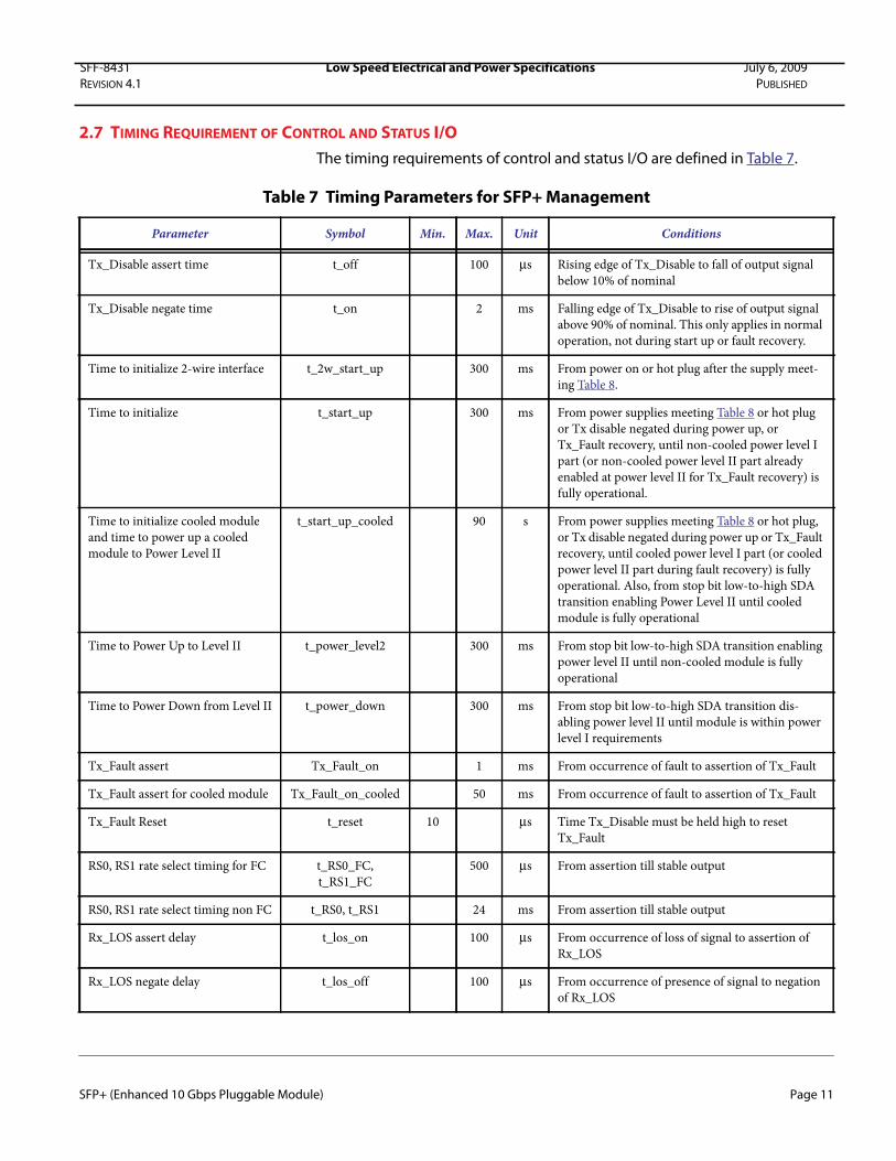
The timing requirements of control and status I/O are defined in Table 7.
Table 7 Timing Parameters for SFP+ Management
Parameter Symbol Min. Max. Unit Conditions
Tx_Disable assert time t_off 100 μs Rising edge of Tx_Disable to fall of output signal
below 10% of nominal
Tx_Disable negate time t_on 2 ms Falling edge of Tx_Disable to rise of output signal
above 90% of nominal. This only applies in normal
operation, not during start up or fault recovery.
Time to initialize 2-wire interface t_2w_start_up 300 ms From power on or hot plug after the supply meet-
ing Table 8.
Time to initialize t_start_up 300 ms From power supplies meeting Table 8 or hot plug
or Tx disable negated during power up, or
Tx_Fault recovery, until non-cooled power level I
part (or non-cooled power level II part already
enabled at power level II for Tx_Fault recovery) is
fully operational.
Time to initialize cooled module
and time to power up a cooled
module to Power Level II
t_start_up_cooled 90 s From power supplies meeting Table 8 or hot plug,
or Tx disable negated during power up or Tx_Fault
recovery, until cooled power level I part (or cooled
power level II part during fault recovery) is fully
operational. Also, from stop bit low-to-high SDA
transition enabling Power Level II until cooled
module is fully operational
Time to Power Up to Level II t_power_level2 300 ms From stop bit low-to-high SDA transition enabling
power level II until non-cooled module is fully
operational
Time to Power Down from Level II t_power_down 300 ms From stop bit low-to-high SDA transition dis-
abling power level II until module is within power
level I requirements
Tx_Fault assert Tx_Fault_on 1 ms From occurrence of fault to assertion of Tx_Fault
Tx_Fault assert for cooled module Tx_Fault_on_cooled 50 ms From occurrence of fault to assertion of Tx_Fault
Tx_Fault Reset t_reset 10 μs Time Tx_Disable must be held high to reset
Tx_Fault
RS0, RS1 rate select timing for FC t_RS0_FC,
t_RS1_FC
500 μs From assertion till stable output
RS0, RS1 rate select timing non FC t_RS0, t_RS1 24 ms From assertion till stable output
Rx_LOS assert delay t_los_on 100 μs From occurrence of loss of signal to assertion of
Rx_LOS
Rx_LOS negate delay t_los_off 100 μs From occurrence of presence of signal to negation
of Rx_LOS
SFP+ (Enhanced 10 Gbps Pluggable Module) Page 11

SFF-8431 Low Speed Electrical and Power Specifications July 6, 2009
REVISION 4.1 PUBLISHED
2.7.1 MODULE POWER ON INITIALIZATION PROCEDURE, TX_DISABLE NEGATED
During power on of the module, Tx_Fault, if implemented, may be asserted (high) as soon as power supply voltages are within specification. For module initialization with Tx_Disable negated, Tx_Fault shall be negated when the transmitter safety circuitry, if implemented, has detected that the transmitter is operating in its normal state. If a transmitter fault has not occurred, Tx_Fault shall be negated within a period t_start_up from the time that VccT exceeds the specified minimum operating voltage (see Table 8). If the Tx_Fault remains asserted after t_start_up, the host shall determine whether the module is cooled by reading the status bit over 2-wire interface. If the module is not cooled, the host may assume that a transmission fault has occurred. If the module is cooled, the host may assume that a transmission fault has occurred if Tx_Fault remains asserted beyond t_start_up_cooled.
The power on initialization timing for a module with Tx_Disable negated is shown in Figure 3.
Figure 3 Power on initialization of module, Tx_Disable negated
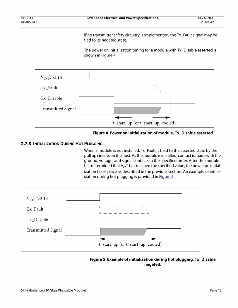
2.7.2 MODULE POWER ON INITIALIZATION PROCEDURE, TX_DISABLE ASSERTED.
For module power on initialization with Tx_Disable asserted, the state of Tx_Fault is not defined while Tx_Disable is asserted. After Tx_Disable is ne-gated, Tx_Fault may be asserted while safety circuit initialization is performed. Tx_Fault shall be negated when the transmitter safety circuitry, if imple-mented, has detected that the transmitter is operating in its normal state. If a transmitter fault has not occurred, Tx_Fault shall be negated within a period t_start_up from the time that Tx_Disable is negated. If Tx_Fault remains as-serted beyond the period t_start_up, the host may assume that a transmission fault has been detected by the module.
VCCT>3.14
Transmitted Signal
Tx_Disable
Tx_Fault
t_start_up (or t_start_up_cooled)
SFP+ (Enhanced 10 Gbps Pluggable Module) Page 12
SFF-8431 Low Speed Electrical and Power Specifications July 6, 2009
REVISION 4.1 PUBLISHED
If no transmitter safety circuitry is implemented, the Tx_Fault signal may be tied to its negated state.
The power on initialization timing for a module with Tx_Disable asserted is shown in Figure 4.
Figure 4 Power on initialization of module, Tx_Disable asserted
2.7.3 INITIALIZATION DURING HOT PLUGGING
When a module is not installed, Tx_Fault is held to the asserted state by the pull up circuits on the host. As the module is installed, contact is made with the ground, voltage, and signal contacts in the specified order. After the module has determined that VccT has reached the specified value, the power on initial-
ization takes place as described in the previous section. An example of initial-ization during hot plugging is provided in Figure 5.
Figure 5 Example of initialization during hot plugging, Tx_Disable negated.
VCCT>3.14
Transmitted Signal
Tx_Disable
Tx_Fault
t_start_up (or t_start_up_cooled)
VCCT>3.14
Transmitted Signal
Tx_Disable
Tx_Fault
t_start_up (or t_start_up_cooled)
SFP+ (Enhanced 10 Gbps Pluggable Module) Page 13
SFF-8431 Low Speed Electrical and Power Specifications July 6, 2009
REVISION 4.1 PUBLISHED
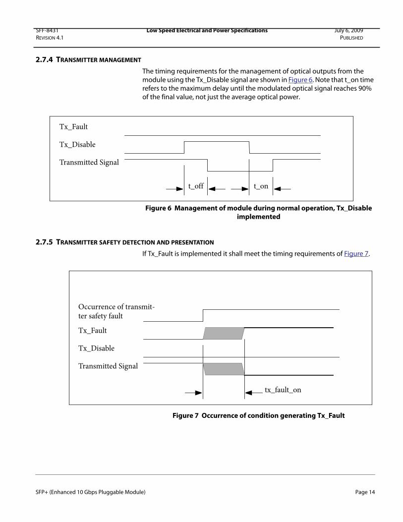
2.7.4 TRANSMITTER MANAGEMENT
The timing requirements for the management of optical outputs from the module using the Tx_Disable signal are shown in Figure 6. Note that t_on time refers to the maximum delay until the modulated optical signal reaches 90% of the final value, not just the average optical power.
Figure 6 Management of module during normal operation, Tx_Disable implemented
2.7.5 TRANSMITTER SAFETY DETECTION AND PRESENTATION
If Tx_Fault is implemented it shall meet the timing requirements of Figure 7.
Figure 7 Occurrence of condition generating Tx_Fault
Transmitted Signal
Tx_Disable
Tx_Fault
t_off t_on
Transmitted Signal
Tx_Disable
Tx_Fault
tx_fault_on
Occurrence of transmit-ter safety fault
SFP+ (Enhanced 10 Gbps Pluggable Module) Page 14
SFF-8431 Low Speed Electrical and Power Specifications July 6, 2009
REVISION 4.1 PUBLISHED
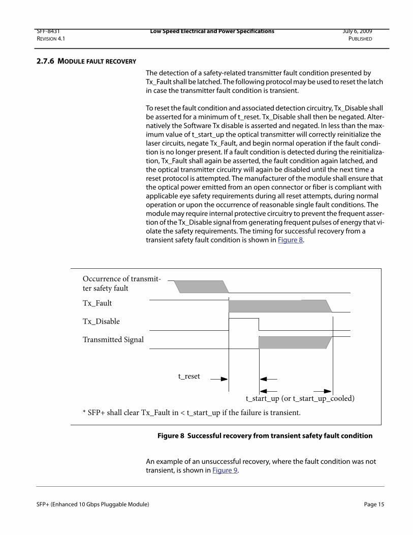
2.7.6 MODULE FAULT RECOVERY
Transmitted Signal
Tx_Disable
Tx_Fault
t_reset
Occurrence of transmit-ter safety fault
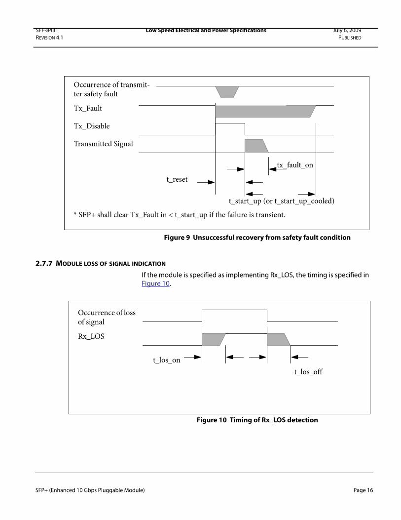
* SFP+ shall clear Tx_Fault in < t_start_up if the failure is transient.
t_start_up (or t_start_up_cooled)
The detection of a safety-related transmitter fault condition presented by Tx_Fault shall be latched. The following protocol may be used to reset the latch in case the transmitter fault condition is transient.
To reset the fault condition and associated detection circuitry, Tx_Disable shall be asserted for a minimum of t_reset. Tx_Disable shall then be negated. Alter-natively the Software Tx disable is asserted and negated. In less than the max-imum value of t_start_up the optical transmitter will correctly reinitialize the laser circuits, negate Tx_Fault, and begin normal operation if the fault condi-tion is no longer present. If a fault condition is detected during the reinitializa-tion, Tx_Fault shall again be asserted, the fault condition again latched, and the optical transmitter circuitry will again be disabled until the next time a reset protocol is attempted. The manufacturer of the module shall ensure that the optical power emitted from an open connector or fiber is compliant with applicable eye safety requirements during all reset attempts, during normal operation or upon the occurrence of reasonable single fault conditions. The module may require internal protective circuitry to prevent the frequent asser-tion of the Tx_Disable signal from generating frequent pulses of energy that vi-olate the safety requirements. The timing for successful recovery from a transient safety fault condition is shown in Figure 8.
Figure 8 Successful recovery from transient safety fault condition
An example of an unsuccessful recovery, where the fault condition was not transient, is shown in Figure 9.
SFP+ (Enhanced 10 Gbps Pluggable Module) Page 15
SFF-8431 Low Speed Electrical and Power Specifications July 6, 2009
REVISION 4.1 PUBLISHED
Figure 9 Unsuccessful recovery from safety fault condition
2.7.7 MODULE LOSS OF SIGNAL INDICATION
If the module is specified as implementing Rx_LOS, the timing is specified in Figure 10.
Figure 10 Timing of Rx_LOS detection
Transmitted Signal
Tx_Disable
Tx_Fault
t_reset
Occurrence of transmit-ter safety fault
* SFP+ shall clear Tx_Fault in < t_start_up if the failure is transient.
tx_fault_on
t_start_up (or t_start_up_cooled)
Rx_LOS
Occurrence of loss of signal
t_los_on
t_los_off
SFP+ (Enhanced 10 Gbps Pluggable Module) Page 16

SFF-8431 Low Speed Electrical and Power Specifications July 6, 2009
REVISION 4.1 PUBLISHED
2.8 SFP+ POWER REQUIREMENT
The module host has two 3.3 V power contacts, one supplying the module transmitter voltage (VccT) and the other supplying the module receiver voltage (VccR). The maximum current capacity, both continuous and peak, for each connector contact is 500 mA.
SFP+ module maximum power consumption shall meet one of the following power classes:
• Power Level I modules – Up to 1.0 W
• Power Level II modules – Up to 1.5 W
To avoid exceeding system power supply limits and cooling capacity, all mod-ules at power up by default shall operate with ≤1.0 W. Hosts supporting Power Level II operation may enable a Power Level II module through the 2-wire in-terface. Power Level II modules shall assert the power level declaration bit of SFF-8472.
The maximum power level is allowed to exceed the classified power level for 500 ms following hot insertion or power up, or Power Level II authorization, however the current is limited to values given by Table 8 and illustrated in Figure 11.
At host power up the host shall supply VccT and VccR to the module within 100 ms of each other.
2.8.1 MODULE POWER SUPPLY REQUIREMENTS
SFP+ module operates from the host supplied VccT and VccR. To protect the host and system operation, each SFP+ module during hot plug and normal op-eration shall follow the requirements listed in Table 8 and illustrated by Figure 11. The requirements for current apply to the current through each inductor of Figure 56 while the power supply voltages are defined at the SFP+ connector.
2.8.2 HOST POWER SUPPLY NOISE OUTPUT
The host shall generate an effective weighted integrated spectrum RMS noise less than 25 mV in the frequency range 10 Hz to 10 MHz, according to the methods of D.17.1
2.8.3 MODULE POWER SUPPLY NOISE OUTPUT
The module shall generate less than 15 mV RMS noise at point X of Figure 56 in the frequency range 10Hz to 10MHz, according to the methods of D.17.2.
2.8.4 POWER SUPPLY NOISE TOLERANCE
SFP+ modules shall meet all electrical requirements and remain fully opera-tional in the presence of a sinusoidal tolerance signal of amplitude given by
SFP+ (Enhanced 10 Gbps Pluggable Module) Page 17

SFF-8431 Low Speed Electrical and Power Specifications July 6, 2009
REVISION 4.1 PUBLISHED
Table 8 swept from 10 Hz to 10 MHz according to the methods of D.17.3. This emulates the worst case noise of the host.
It is also desirable for a module and host to each tolerate a degree of random or semi-random noise on both VccT and VccR simultaneously, but the charac-teristics of this noise are beyond the scope of this document.
Table 8 SFP+ Module Power Supply Requirements
Parameters Symbol Conditions Min Max Units
Power Level I Module
Power supply noise tolerance including ripple [peak-
to-peak]
see D.17.3 66 mV
Power supply voltages including ripple, droop and
noise below 100 kHz
VccT,
VccR
Note 1 3.14 3.46 V
Instantaneous peak current at hot plug Note 2, 3 400 mA
Sustained peak current at hot plug Note 2, 3, 5 330 mA
Module maximum power consumption 1.0 W
Power Level II Module
Power supply noise tolerance including ripple [peak-
to-peak]
see D.17.3 66 mV
Power supply voltages including ripple, droop and
noise below 100 kHz
VccT,
VccR
Note 1 3.14 3.46 V
Instantaneous peak current at hot plug Note 2, 3 400 mA
Sustained peak current at hot plug Note 2, 3, 5 330 mA
Instantaneous peak current on enabling Power Level II Note 2, 3, 5 600 mA
Module sustained peak current on enabling Power
Level II
Note 2, 3, 5 500 mA
Module maximum power consumption 1.5 W
Maximum power consumption at power up Note 4 1 W
1. Set point is measured at the input to the connector on the host board reference to Vee. Droop is any temporary drop in voltage of the
power supply such as that caused by plugging in another module or when enabling another module to Power Level II.
2. The requirements for current apply to the current through each inductor of Figure 56.3. The maximum currents are the allowed currents for each power supply VccT or VccR, therefore the total module peak currents can be
twice this value. The instantaneous peak current is allowed to exceed the specified maximum current capacity of the connector contact
for a short period, see Figure 11.
4. Maximum module power consumption shall not exceed 1.0 W from 500ms after power up until level II operation is enabled.
5. Not to exceed the sustained peak limit for more than 50 μs; may exceed this limit for shorter durations.
SFP+ (Enhanced 10 Gbps Pluggable Module) Page 18

SFF-8431 Low Speed Electrical and Power Specifications July 6, 2009
REVISION 4.1 PUBLISHED
Figure 11 Instantaneous and sustained peak current for VccT or VccR
2.9 ESD
The SFP+ module and host SFI contacts (High Speed Contacts) shall withstand 1000 V electrostatic discharge based on Human Body Model per JEDEC JESD22-A114-B.
The SFP+ module and all host contacts with exception of the SFI contacts (High Speed Contacts) shall withstand 2 kV electrostatic discharge based on Human Body Model per JEDEC JESD22-A114-B.
The SFP+ module shall meet ESD requirements given in EN61000-4-2, criterion B test specification such that units are subjected to 15 kV air discharges during operation and 8 kV direct contact discharges to the case.
Initialization timewindow (500 ms)
Hot plug time or time ofinitialization of PowerLevel II
Instantaneous peak duration <50 μs
Limit for instantaneouspeak current
Limit for sustainedpeak current
Long-term limitdetermined by modulepower limit (depends on other Vcc current)
0 A or current of Power Level II module in Power Level I mode
SFP+ (Enhanced 10 Gbps Pluggable Module) Page 19
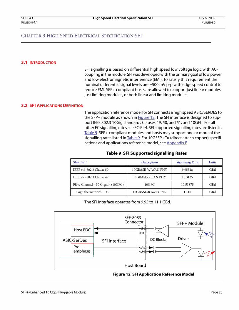
SFF-8431 High Speed Electrical Specification SFI July 6, 2009
REVISION 4.1 PUBLISHED
CHAPTER 3 HIGH SPEED ELECTRICAL SPECIFICATION SFI
3.1 INTRODUCTION
SFI signalling is based on differential high speed low voltage logic with AC-coupling in the module. SFI was developed with the primary goal of low power and low electromagnetic interference (EMI). To satisfy this requirement the nominal differential signal levels are ~500 mV p-p with edge speed control to reduce EMI. SFP+ compliant hosts are allowed to support just linear modules, just limiting modules, or both linear and limiting modules.
3.2 SFI APPLICATIONS DEFINITION
The application reference model for SFI connects a high speed ASIC/SERDES to the SFP+ module as shown in Figure 12. The SFI interface is designed to sup-port IEEE 802.3 10Gig standards Clauses 49, 50, and 51, and 10GFC. For all other FC signalling rates see FC-PI-4. SFI supported signalling rates are listed in Table 9. SFP+ compliant modules and hosts may support one or more of the signalling rates listed in Table 9. For 10GSFP+Cu (direct attach copper) specifi-cations and applications reference model, see Appendix E.
The SFI interface operates from 9.95 to 11.1 GBd.
Figure 12 SFI Application Reference Model
Table 9 SFI Supported signalling Rates
Standard Description signalling Rate Units
IEEE std-802.3 Clause 50 10GBASE-W WAN PHY 9.95328 GBd
IEEE std-802.3 Clause 49 10GBASE-R LAN PHY 10.3125 GBd
Fibre Channel - 10 Gigabit (10GFC) 10GFC 10.51875 GBd
10Gig Ethernet with FEC 10GBASE-R over G.709 11.10 GBd
ASIC/SerDes Driver
SFP+ Module
Host Board
SFF-8083
DC Blocks
Host EDC
Pre-emphasis
SFI Interface
Connector
SFP+ (Enhanced 10 Gbps Pluggable Module) Page 20

SFF-8431 High Speed Electrical Specification SFI July 6, 2009
REVISION 4.1 PUBLISHED
3.3 SFI TEST POINTS DEFINITION AND MEASUREMENTS
SFI reference compliance test points are defined with the Host Compliance Board and the Module Compliance Board for measurement consistency, see Appendix C. The reference test boards provide a set of overlapping measure-ments for ASIC/SerDes, module, and host validation to ensure interoperability. For improved measurement accuracy the actual reference test card responses may be calibrated out of the measurements and replaced with functions that represent the ideal responses defined in Appendix C for the reference test cards.
Points A, B, C, and D require AC coupled test equipment. All SFI test equipment must have 50 Ω single ended impedance on all test ports.
The reference impedance for differential measurements and S-parameters is 100 Ω, and the reference impedance for common mode measurements and S-parameters is 25 Ω.
The bandwidth of measurement instrument shall be 12 GHz unless specified otherwise.
SFI reference points are listed in Table 10.
3.3.1 HOST COMPLIANCE POINTS
Host system transmitter and receiver compliance are defined by tests in which a Host Compliance Board is inserted as shown in Figure 13 in place of the SFP+ module. The Host Compliance Board meets the specifications of Appendix C.
The compliance points are B and C.
Table 10 SFI Reference Points
Compliance point Designation
ASIC/SerDes output A
Host output B
Host input C
ASIC/SerDes input D
Module input B’
Module output C’
Module input calibration B” (double quotation)
Host input calibration C” (double quotation)
SFP+ (Enhanced 10 Gbps Pluggable Module) Page 21

SFF-8431 High Speed Electrical Specification SFI July 6, 2009
REVISION 4.1 PUBLISHED
Figure 13 Host Compliance Board
SFP+ host compliance points are defined as the following:
• B: Host transmitter output at the output of the Host Compliance Board. Specifications for B are given in 3.5.1.
• C: Host receiver input at the input of the Host Compliance Board. Specifi-cations for C are given in 3.5.2.
3.3.2 MODULE COMPLIANCE POINTS
Module transmitter and receiver compliance are defined by tests in which the module is inserted into the Module Compliance Board as shown in Figure 14. The Module Compliance Board meets the specifications of Appendix C. The compliance points for the module are B’ and C’.
ASIC/SerDes
B
C
Host Under Test
Connector
Host Compliance BoardMeasurementInstrumentation
*
* C” equivalent is located about 1 inch past the SFP+ connector on the host board.
DC Blocks
SFP+ (Enhanced 10 Gbps Pluggable Module) Page 22
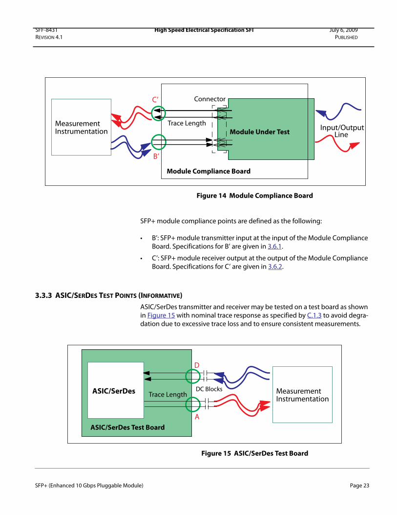
SFF-8431 High Speed Electrical Specification SFI July 6, 2009
REVISION 4.1 PUBLISHED
Figure 14 Module Compliance Board
SFP+ module compliance points are defined as the following:
• B’: SFP+ module transmitter input at the input of the Module Compliance Board. Specifications for B’ are given in 3.6.1.
• C’: SFP+ module receiver output at the output of the Module Compliance Board. Specifications for C’ are given in 3.6.2.
3.3.3 ASIC/SERDES TEST POINTS (INFORMATIVE)
ASIC/SerDes transmitter and receiver may be tested on a test board as shown in Figure 15 with nominal trace response as specified by C.1.3 to avoid degra-dation due to excessive trace loss and to ensure consistent measurements.
Figure 15 ASIC/SerDes Test Board
B’
C’
Module Compliance Board
Connector
Module Under Test
Trace LengthMeasurementInstrumentation
Input/OutputLine
ASIC/SerDes
A
D
ASIC/SerDes Test Board
Trace Length MeasurementInstrumentation
DC Blocks
SFP+ (Enhanced 10 Gbps Pluggable Module) Page 23

SFF-8431 High Speed Electrical Specification SFI July 6, 2009
REVISION 4.1 PUBLISHED
SFI ASIC/SerDes test points are defined as the following:
• A: SerDes transmitter output at the output of the ASIC/SerDes Test Board. Recommendations for A are given in B.2.
• D: ASIC/SerDes receiver input at the input of the ASIC/SerDes Test Board. Recommendations for D are given in B.3.
3.3.4 HOST INPUT CALIBRATION POINT
Host receiver input tolerance signals are calibrated through the Host Compli-ance Board at the output of the Module Compliance Board as shown in Figure 16. The host input calibration point is at C” with specifications for C” given in 3.5.2. The response between the connector and C” is specified by C.1.2.
Figure 16 Host input calibration point C” and crosstalk source calibration point B”
3.3.5 MODULE INPUT CALIBRATION POINT
Module transmitter input tolerance signals are calibrated through the Module Compliance Board at the output of the Host Compliance Board as shown in Figure 17. The module input calibration point is at B” with specifications for B” given in 3.6.1. The response between the connector and B” is specified by C.1.1.
Module Compliance Board
Connector
Trace Length
C”Stressed Signal Generator
Measurement
Instrumentation
Crosstalk Sourceor Scope
DC Blocks
Host Compliance Board B”
2x50 Ω
SFP+ (Enhanced 10 Gbps Pluggable Module) Page 24

SFF-8431 High Speed Electrical Specification SFI July 6, 2009
REVISION 4.1 PUBLISHED
Figure 17 Module input calibration point B” and crosstalk source calibration point C”
3.4 SFI TERMINATION AND DC BLOCKING
The SFI link uses nominal 100 Ω differential source and load terminations on both the host board and the module. The SFI transmitter provides both differ-ential and common mode termination. The SFI transmitter and receiver termi-nation specifications for each of the compliance points are given by:
• Host – 3.5 SFP+ Host System Specifications
• Module – 3.6 SFP+ Module Specifications .
Host SerDes termination recommendations are given by:
• ASIC/SerDes – Appendix B
SFP+ modules shall incorporate blocking capacitors or equivalent on all SFI in-puts and outputs as shown in Figure 18. The SFI transmitter is represented by terminations Zp and Zn which form a 100 Ω differential source. Each termina-
tion has a nominal value of 50 Ω, and therefore the common mode impedance is 25 Ω. The SFI receiver is represented with termination Zdiff with nominal 100
Ω value. This representation is not intended to preclude the use of other im-plementations which may provide common mode termination, however the SFI specification does not require any common mode termination at the re-ceiver. If common mode terminations are provided, it may reduce common mode voltage and EMI.
Module Compliance Board
Connector
Trace LengthStressed
Crosstalk Source
Signal Generator
2x50 Ωor Scope
B”
Measurement Instrumentation
C”
Host Compliance Board
SFP+ (Enhanced 10 Gbps Pluggable Module) Page 25
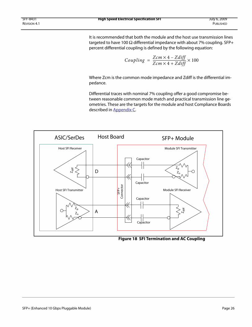
SFF-8431 High Speed Electrical Specification SFI July 6, 2009
REVISION 4.1 PUBLISHED
It is recommended that both the module and the host use transmission lines targeted to have 100 Ω differential impedance with about 7% coupling. SFP+ percent differential coupling is defined by the following equation:
Where Zcm is the common mode impedance and Zdiff is the differential im-pedance.
Differential traces with nominal 7% coupling offer a good compromise be-tween reasonable common mode match and practical transmission line ge-ometries. These are the targets for the module and host Compliance Boards described in Appendix C.
Figure 18 SFI Termination and AC Coupling
CouplingZcm 4× Zdiff–
Zcm 4× Zdiff+-------------------------------------- 100×=
Module SFI Receiver
Capacitor
Capacitor
Capacitor
Capacitor
Module SFI Transmitter
Zp
Zn
Zd
iff
Host SFI Transmitter
D
Host SFI Receiver
Zd
iff
AZp
Zn
Host BoardASIC/SerDes SFP+ Module
SF
P+
Co
nn
ect
or
SFP+ (Enhanced 10 Gbps Pluggable Module) Page 26
SFF-8431 High Speed Electrical Specification SFI July 6, 2009
REVISION 4.1 PUBLISHED
3.5 SFP+ HOST SYSTEM SPECIFICATIONS
SFP+ host system transmitter specifications at compliance point B are given in 3.5.1. SFP+ Host system receiver specifications at compliance point C are given in 3.5.2.
All specifications are to be met at the host compliance test points defined in 3.3.1.
The solder pads for the high speed traces in the SFF-8431 Module Compliance Board are 1.1x0.4 mm to improve high frequency performance instead of 2.0x0.5 mm as defined in the SFF-8083 for improved manufacturability. Trade-off between host performance and manufacturability are left to the host de-signer. For detailed geometry of the Module Compliance Board, see the Gerber files in C.3.4.
Warning: The host expects DC blocking in the module, and for improved performance the Host Compliance Board is not required to incorporate DC blocks. DC blocking within the test equipment or between the host and the equipment is necessary for all host SFI signals.
3.5.1 HOST TRANSMITTER OUTPUT SPECIFICATIONS AT B
SFP+ host transmitter electrical specifications defined at compliance point B are given in Table 11 and Table 12. These specifications are defined at the output of the Host Compliance Board specified in C.2. Host transmitters must provide adequate low frequency signal response for the applications sup-ported.
SFP+ (Enhanced 10 Gbps Pluggable Module) Page 27

SFF-8431 High Speed Electrical Specification SFI July 6, 2009
REVISION 4.1 PUBLISHED
The specification of common mode output return loss reduces EMI and noise by absorbing common mode reflections and noise.
The SFI jitter specifications at reference point B are listed in Table 12 and the compliance mask is shown in Figure 19. As baseline wander can create low
probability eye closure which is not detected by the 5x10⁻⁵ mask hit ratio, baseline wander must be controlled so as not to significantly degrade the signal at B.
Table 11 Host Transmitter Output Electrical Specifications at B
Parameter - B Symbol Conditions Min Max Units
Termination Mismatch at 1 MHz ΔZM See D.16, Figure 55 5 %
Single Ended Output Voltage Range -0.3 4.0 V
Output AC Common Mode Voltage See D.15 15 mV (RMS)
Differential Output S-parameter SDD22
0.01 to 2 GHz -12 dB
2 to 11.1 GHz see 1 dB
Common Mode Output S-parameter SCC22 0.01 to 2.5 GHz see 2 dB
2.5 to 11.1 GHz -3 dB
1. Reflection coefficient given by equation SDD22(dB) < -6.68 + 12.1 × log10(f/5.5), with f in GHz.
2. Reflection coefficient given by equation SCC22(dB) < -7 + 1.6 × f, with f in GHz.
SFP+ (Enhanced 10 Gbps Pluggable Module) Page 28

SFF-8431 High Speed Electrical Specification SFI July 6, 2009
REVISION 4.1 PUBLISHED
Figure 19 Transmitter Differential Output Compliance Mask at B and B”
Table 12 Host Transmitter Output Jitter and Eye Mask Specifications at B
Parameters- B Symbol Conditions Min Target
Value
Max Units
Crosstalk Source Rise/Fall time (20% to 80%) Tr, Tf See 1, 2, D.6 34 ps
Crosstalk Source Amplitude (p-p differential) See 1, 2, D.7 1000 mV
Signal Rise/Fall time (20% to 80%) Tr, Tf See D.6 34 ps
Total Jitter TJ See D.5 0.28 UI(p-p)
Data Dependent Jitter DDJ See D.3 0.1 UI(p-p)
Data Dependent Pulse Width Shrinkage DDPWS 0.055 UI (p-p)
Uncorrelated Jitter UJ See 3 and D.4 0.023 UI (RMS)
Transmitter Qsq Qsq See 4 50
Parameters- B Symbol Conditions Value Units
Eye Mask X1
Mask hit ratio of 5×10⁻⁵,
See D.2 and
Figure 19
0.12 UI
Eye Mask X2 0.33 UI
Eye Mask Y1 95 mV
Eye Mask Y2 350 mV
1. Measured at C" with Host Compliance Board and Module Compliance Board pair, see Figure 17.
2. Since the minimum module output transition time is faster than the crosstalk transition time the amplitude of crosstalk source is
increased to achieve the same slew rate.
3. It is not possible to have the maximum UJ and meet the TJ specifications if the UJ is all Gaussian.
4. Qsq=1/RN if the one level and zero level noises are identical and see D.8.
-Y2
-Y1
0
Y1
Y2
0.0 X1 X2 1-X2 1-X1 1.0
Normalized Time (UI)
Vo
ltag
e
SFP+ (Enhanced 10 Gbps Pluggable Module) Page 29

SFF-8431 High Speed Electrical Specification SFI July 6, 2009
REVISION 4.1 PUBLISHED
3.5.2 HOST RECEIVER INPUT SPECIFICATIONS AT C AND C”
The SFP+ Host receiver electrical specifications at compliance point C and C” for both linear and limiting modules are given in Table 13. The host shall pro-vide differential termination and must constrain differential to common mode conversion for quality signal termination and low EMI, as given in Table 13. Common mode termination on the receiver is not required see Figure 18.
Signals used as input tolerance test conditions are calibrated at C” with the Host Compliance Board connected through a Module Compliance Board to measurement instrumentation. Specifications at C” supporting limiting mod-ules are given in Table 14. Specifications at C” supporting linear module are given in Table 15.
SFP+ compliant hosts are allowed to support just linear modules, just limiting modules, or both linear and limiting modules.
Jitter specifications to support the limiting module are listed in Table 14. Figure 20 gives the host compliance eye mask requirements to support the limiting module. The host shall operate at and between the sensitivity and overload limits. The SFP+ limiting host shall tolerate sinusoidal jitter given by Figure 21. Test procedures for the host for limiting module are given in D.11.
Table 13 Host Receiver Input Electrical Specifications at C and C”
Parameters - C and C" Symbol Conditions Min Target Max Units
Single Ended Input Voltage Range Referenced to VeeR -0.3 4.0 V
Input AC Common Mode Voltage Tolerance See 1 and D.15.3 7.5 mV (RMS)
Damage Threshold (p-p differential) See 1 2000 mV
Differential Input S-parameter SDD11
0.01 to 2 GHz -12 dB
2 to 11.1 GHz see 2 dB
Reflected Differential to Common Mode
Conversion SCD11 0.1 to 11.1 GHz -10 dB
1. Measured at C" with the Module Compliance Board. 2. Reflection Coefficient given by equation SDD11(dB)< -6.68 + 12.1 × log10(f/5.5), with f in GHz .
SFP+ (Enhanced 10 Gbps Pluggable Module) Page 30

SFF-8431 High Speed Electrical Specification SFI July 6, 2009
REVISION 4.1 PUBLISHED
Table 14 Host receiver supporting limiting module input compliance test signal calibrated at C”
Parameters - C" Symbol Conditions Target
Value
Max Units
Crosstalk Source Rise/Fall time (20% to 80%) Tr, Tf See D.6 34 ps
Crosstalk Source Amplitude (p-p differential) See 1 700 mV
AC Common Mode Voltage See 2 and D.15 7.5 mV
(RMS)
99% Jitter J2 See 3, D.5, D.11 0.42 UI (p-p)
Pulse Width Shrinkage Jitter DDPWS See 4, D.3 0.3 UI (p-p)
Total Jitter TJ BER 1×10⁻¹² see D.5, D.11 0.70 UI (p-p)
Eye Mask X1 Mask hit ratio of 1×10⁻¹²,
See D.2, D.11
0.35 UI
Eye Mask Amplitude Sensitivity 5,8 Y1 150 mV
Eye Mask Amplitude Overload 6,7,8 Y2 425 mV
1. Measured at B" with Host Compliance Board and Module Compliance Board pair, see Figure 16.
2. The tester is not expected to generate this common mode voltage however its output must not exceed this value.
3. Includes sinusoidal jitter, per Figure 21, when measured with the reference PLL specified by the given standard.
4. In practice the test implementer may trade DDPWS with other pulse width shrinkage from the sinusoidal interferer.
5. Eye mask amplitude sensitivity tests the host receiver with the minimum eye opening expected from a module within the constraint set by
Y2.
6. Eye mask amplitude overload tests the host receiver tolerance to the largest peak signal levels expected from the module within the
constraint set by Y1.
7. It is not expected that module Rx output will exhibit both maximum peak level and minimum eye opening.
8. Sensitivity and overload are tested separately, see D.11.
SFP+ (Enhanced 10 Gbps Pluggable Module) Page 31

SFF-8431 High Speed Electrical Specification SFI July 6, 2009
REVISION 4.1 PUBLISHED
Figure 20 Host Receiver Input Compliance Mask at C” Supporting Limiting Module
Figure 21 SR and LR Host Sinusoidal Jitter Tolerance Mask
Table 15 defines the input compliance test signal as calibrated at C” for a host that supports linear modules. The parameters in Table 15 include the effects of a worst case module that operates in conjunction with optical TP3 tester(s) de-fined for the LRM and LR standards. SR specifications are covered by the fact that LR links have high noise, and on the other extreme, LRM links have high distortion. Test procedures for the linear host are given in D.13. For illustrative purpose, Figure 24 shows the host test calibration line along which specific host test points for LRM are defined.
-Y2
-Y1
0
Y1
Y2
0.0 X1 1-X1 1.0
Normalized Time (UI)
Vo
ltag
e
4
Frequency (MHz)
sin
uso
idal
jit
ter
tole
ran
ce (
UIp
-p)
5.0-20 dB/decade
0.4
0.05
400.04
SFP+ (Enhanced 10 Gbps Pluggable Module) Page 32

SFF-8431 High Speed Electrical Specification SFI July 6, 2009
REVISION 4.1 PUBLISHED
For LR test conditions, the SFP+ linear host shall operate with sinusoidal jitter given by Figure 21 while the stress conditions given in Table 15 are applied. For LRM test conditions, the host shall operate with sinusoidal jitter as defined in IEEE802.3, clause 68, with the stressors and noises in Figure 52 including those in the TP3 tester turned off.
Only two specific test conditions for each LRM stressor are defined in Table 15. In general, however, a host must meet operational requirements with any compliant module. It is expected that lower dWDP modules will exist. How-ever, this specification has not defined host test conditions below dWDP of 0.6 to 0.8 dB. At low dWDP values, guard bands between module specifications and host requirements are left to the host implementation.
SFP+ (Enhanced 10 Gbps Pluggable Module) Page 33
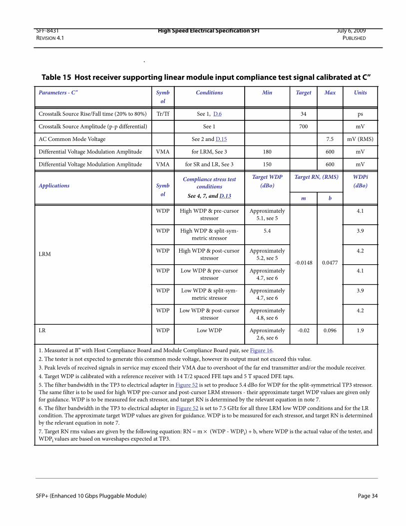
SFF-8431 High Speed Electrical Specification SFI July 6, 2009
REVISION 4.1 PUBLISHED
.
Table 15 Host receiver supporting linear module input compliance test signal calibrated at C”
Parameters - C" Symb
ol
Conditions Min Target Max Units
Crosstalk Source Rise/Fall time (20% to 80%) Tr/Tf See 1, D.6 34 ps
Crosstalk Source Amplitude (p-p differential) See 1 700 mV
AC Common Mode Voltage See 2 and D.15 7.5 mV (RMS)
Differential Voltage Modulation Amplitude VMA for LRM, See 3 180 600 mV
Differential Voltage Modulation Amplitude VMA for SR and LR, See 3 150 600 mV
Applications Symb
ol
Compliance stress test
conditions
See 4, 7, and D.13
Target WDP
(dBo)
Target RN, (RMS) WDPi
(dBo)
m b
LRM
WDP High WDP & pre-cursor
stressor
Approximately
5.1, see 5
-0.0148 0.0477
4.1
WDP High WDP & split-sym-
metric stressor
5.4 3.9
WDP High WDP & post-cursor
stressor
Approximately
5.2, see 5
4.2
WDP Low WDP & pre-cursor
stressor
Approximately
4.7, see 6
4.1
WDP Low WDP & split-sym-
metric stressor
Approximately
4.7, see 6
3.9
WDP Low WDP & post-cursor
stressor
Approximately
4.8, see 6
4.2
LR WDP Low WDP Approximately
2.6, see 6
-0.02 0.096 1.9
1. Measured at B” with Host Compliance Board and Module Compliance Board pair, see Figure 16.
2. The tester is not expected to generate this common mode voltage, however its output must not exceed this value.
3. Peak levels of received signals in service may exceed their VMA due to overshoot of the far end transmitter and/or the module receiver.
4. Target WDP is calibrated with a reference receiver with 14 T/2 spaced FFE taps and 5 T spaced DFE taps.
5. The filter bandwidth in the TP3 to electrical adapter in Figure 52 is set to produce 5.4 dBo for WDP for the split-symmetrical TP3 stressor.
The same filter is to be used for high WDP pre-cursor and post-cursor LRM stressors - their approximate target WDP values are given only
for guidance. WDP is to be measured for each stressor, and target RN is determined by the relevant equation in note 7.
6. The filter bandwidth in the TP3 to electrical adapter in Figure 52 is set to 7.5 GHz for all three LRM low WDP conditions and for the LR
condition. The approximate target WDP values are given for guidance. WDP is to be measured for each stressor, and target RN is determined
by the relevant equation in note 7.
7. Target RN rms values are given by the following equation: RN = m × (WDP - WDPi) + b, where WDP is the actual value of the tester, and
WDPi values are based on waveshapes expected at TP3.
SFP+ (Enhanced 10 Gbps Pluggable Module) Page 34
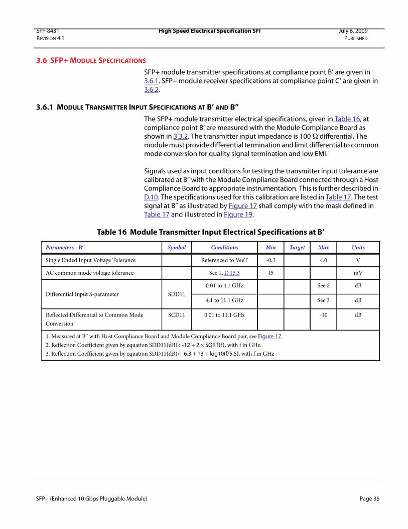
SFF-8431 High Speed Electrical Specification SFI July 6, 2009
REVISION 4.1 PUBLISHED
3.6 SFP+ MODULE SPECIFICATIONS
SFP+ module transmitter specifications at compliance point B’ are given in 3.6.1. SFP+ module receiver specifications at compliance point C’ are given in 3.6.2.
3.6.1 MODULE TRANSMITTER INPUT SPECIFICATIONS AT B’ AND B”
The SFP+ module transmitter electrical specifications, given in Table 16, at compliance point B’ are measured with the Module Compliance Board as shown in 3.3.2. The transmitter input impedance is 100 Ω differential. The module must provide differential termination and limit differential to common mode conversion for quality signal termination and low EMI.
Signals used as input conditions for testing the transmitter input tolerance are calibrated at B” with the Module Compliance Board connected through a Host Compliance Board to appropriate instrumentation. This is further described in D.10. The specifications used for this calibration are listed in Table 17. The test signal at B” as illustrated by Figure 17 shall comply with the mask defined in Table 17 and illustrated in Figure 19.
Table 16 Module Transmitter Input Electrical Specifications at B’
Parameters - B’ Symbol Conditions Min Target Max Units
Single Ended Input Voltage Tolerance Referenced to VeeT -0.3 4.0 V
AC common mode voltage tolerance See 1, D.15.3 15 mV
Differential Input S-parameter SDD11
0.01 to 4.1 GHz See 2 dB
4.1 to 11.1 GHz See 3 dB
Reflected Differential to Common Mode
Conversion
SCD11 0.01 to 11.1 GHz -10 dB
1. Measured at B” with Host Compliance Board and Module Compliance Board pair, see Figure 17.
2. Reflection Coefficient given by equation SDD11(dB)< -12 + 2 × SQRT(f ), with f in GHz.
3. Reflection Coefficient given by equation SDD11(dB)< -6.3 + 13 × log10(f/5.5), with f in GHz
SFP+ (Enhanced 10 Gbps Pluggable Module) Page 35

SFF-8431 High Speed Electrical Specification SFI July 6, 2009
REVISION 4.1 PUBLISHED
Figure 22 Module Transmitter Differential Input Compliance Mask at B”
Table 17 Module Transmitter Input Tolerance Signal Calibrated at B”
Parameters- B" Symbol Conditions Target
Value
Max Units
Crosstalk Source Rise/Fall time (20% to 80%) Tr, Tf See 1, 2 and D.6 34 ps
Crosstalk Source Amplitude (p-p differential) See 1, 2 1000 mV
AC Common Mode Voltage See 3 and D.15.2 15 mV (RMS)
Total Jitter TJ See D.5 0.28 UI (p-p)
Data Dependent Jitter DDJ See D.3 0.10 UI (p-p)
Pulse Width Shrinkage Jitter DDPWS 0.055 UI (p-p)
Uncorrelated Jitter UJ See 4 and D.4 0.023 UI (RMS)
Parameters- B" Symbol Conditions Value Units
Eye Mask X1
Mask hit ratio of 5×10⁻⁵,
See D.2
0.12 UI
Eye Mask X2 0.33 UI
Eye Mask Y1 95 mV
Eye Mask Y2 350 mV
1. Measured at C" with Host Compliance Board and Module Compliance Board pair, see Figure 17.
2. Since the minimum module output transition time is faster than the crosstalk transition time the amplitude of crosstalk source is
increased to achieve the same slew rate.
3. The tester is not expected to generate this common mode voltage however its output must not exceed this value
4. It is not possible to have the maximum UJ and meet the TJ specifications if the UJ is all Gaussian.
-Y2
-Y1
0
Y1
Y2
0.0 X1 X2 1-X2 1-X1 1.0
Normalized Time (UI)
Vo
ltag
e
SFP+ (Enhanced 10 Gbps Pluggable Module) Page 36

SFF-8431 High Speed Electrical Specification SFI July 6, 2009
REVISION 4.1 PUBLISHED
3.6.2 MODULE RECEIVER OUTPUT SPECIFICATIONS AT C’
The SFP+ receiver electrical output specifications at compliance point C’ are given in Table 18. The module must provide differential termination and common mode termination for quality signal termination and low EMI, as given in Table 18.
Common Mode Output Reflection Coefficient helps absorb reflection and noise improving EMI.
Jitter specifications for limiting modules are listed in Table 19. Figure 23 gives the compliance eye mask for limiting modules output. Requirements for linear modules are given in Table 20.
Both limiting and linear modules must provide adequate low frequency signal response for the applications supported, to control the effects of baseline wander.
Table 18 Module Receiver Output Electrical Specifications at C’
Parameters - C’ Symbol Conditions Min Target Max Units
Crosstalk source rise/fall time (20% to 80%) Tr, Tf See 1, D.6, 34 ps
Crosstalk Source Amplitude (p-p differential) See 1 700 mV
Termination Mismatch at 1 MHz ΔZM See D.16, Figure 55 5 %
Single Ended Output Voltage Tolerance -0.3 4.0 V
Output AC Common Mode Voltage See D.15 7.5 mV (RMS)
Differential Output S-parameter SDD22
0.01 to 4.1 GHz See 2 dB
4.1 to 11.1 GHz See 3 dB
Common Mode Output Reflection
Coefficient
SCC22 0.01 to 2.5 GHz See 4 dB
2.5 to 11.1 GHz -3 dB
1. Measured at B” with the Host Compliance Board and Module Compliance Board pair, see Figure 16.
2. Reflection Coefficient given by equation SDD22(dB)< -12 + 2 × SQRT(f ), with f in GHz.
3. Reflection Coefficient given by equation SDD22(dB)< -6.3 + 13 × log10(f/5.5), with f in GHz
4. Reflection coefficient given by equation SCC22(dB) < -7 + 1.6 × f, with f in GHz.
SFP+ (Enhanced 10 Gbps Pluggable Module) Page 37

SFF-8431 High Speed Electrical Specification SFI July 6, 2009
REVISION 4.1 PUBLISHED
Figure 23 Limiting Module Receiver Differential Output Compliance Mask at C’
Table 19 Limiting Module Receiver Output Jitter and Eye Mask Specifications at C’
Parameters - C’ Symbol Conditions Min Target Max Units
Output Rise and Fall time (20% to 80%) Tr, Tf See D.6 28 ps
Total Jitter TJ See D.5, D.12 0.70 UI (p-p)
99% Jitter J2 See D.5, D.12 0.42 UI (p-p)
Parameters - C’ Symbol Conditions Value Units
Eye Mask X1
Mask hit ratio of
1×10⁻¹²
See D.2, D.12
0.35 UI
Eye Mask Y1 150 mV
Eye Mask Y2 425 mV
-Y2
-Y1
0
Y1
Y2
0.0 X1 1-X1 1.0
Normalized Time (UI)
Vo
ltag
e
SFP+ (Enhanced 10 Gbps Pluggable Module) Page 38

SFF-8431 High Speed Electrical Specification SFI July 6, 2009
REVISION 4.1 PUBLISHED
Linear module test parameters are given by Table 20. Compliance methods for a linear module are given in Appendix D.14.
Appendix D.14.2 defines RN for a linear module receiver. The limits for RN are functions of measured dWDP for the module, expressed in optical decibels. As an example, the trade-off between the parameters for LRM are shown in Figure 24. To pass, RN must be below the respective limit line.
dWDP and RN shall meet the specifications in Table 20 and can be calculated by
for each TP3 test condition for which compliance is required. For example, if compliance is required for LRM, the module must meet specifications with all three stressors and under the sensitivity and overload test conditions specified in IEEE Std 802.3 68.6.9.
Table 20 Linear Module Receiver Specifications at C’
Parameters - C’ Symbol Conditions RN
m1 b1 m2 b2 RNmax
Relative Noise SR RN
See D.14.1
-0.02 0.078 -0.02 0.078 0.078
Relative Noise LR -0.02 0.083 -0.02 0.083 0.083
Relative Noise LRM with pre-cursor stressor -0.0153 0.0475 -0.0092 0.0457 0.0475
Relative Noise LRM with split-symmetrical stressor -0.017 0.0475 -0.01 0.0455 0.0475
Relative Noise LRM with post-cursor stressor -0.0153 0.0475 -0.0092 0.0457 0.0475
Parameters - C’ Symbol Conditions Min Max Unit
Difference Waveform Distortion Penalty for SR and
LR
dWDP
See 1 and
D.14.2
2.7 dBo
Difference Waveform Distortion Penalty for LRM dWDP 1.5 dBo
Differential Voltage Modulation Amplitude For SR
and LR
VMA See D.7 150 600 mV
Differential Voltage Modulation Amplitude For LRM VMA 180 600 mV
Differential peak to peak voltage Vpk-pk See D.14.3 600 mV
1. Defined with reference receiver with 14 T/2 spaced FFE taps and 5 T spaced DFE taps.
RN min m1 dWDP× b1+( ) m2 dWDP× b2+( ) RNmax,[ , ]≤
SFP+ (Enhanced 10 Gbps Pluggable Module) Page 39

SFF-8431 High Speed Electrical Specification SFI July 6, 2009
REVISION 4.1 PUBLISHED
Figure 24 LRM module receiver RN and dWDP compliance and host receiver test calibration
For illustrative purpose, Figure 24 shows the host test calibration line along which specific host test points for LRM are defined. The gap between the host and module lines is because the host is tested with linear impairments, which given the same dWDP, are more benign to a host than non-linear impairments which are possible from a module.
Module Fails
Module Passes
SFP+ (Enhanced 10 Gbps Pluggable Module) Page 40

SFF-8431 SFP+ 2-wire Interface July 6, 2009
REVISION 4.1 PUBLISHED
CHAPTER 4 SFP+ 2-WIRE INTERFACE
4.1 INTRODUCTION
The SFP+ management interface is a two-wire interface, similar to I2C. SFP+ management memory map is specified by SFF-8472. Nomenclature for all reg-isters more than 1 bit long are MSB...LSB (MSB transmitted first).
4.2 2-WIRE ELECTRICAL SPECIFICATIONS
The SFP+ 2-wire interface specifications are given in Table 21. This specifica-tion ensures compatibility between host masters and SFP+ SCL/SDA lines and
compatibility with I2C. All voltages are referenced to VeeT.
Table 21 2-Wire Interface Electrical Specifications
Parameter Symbol Min. Max. Unit Conditions
Host 2-wire Vcc Vcc_Host_2w 3.14 3.46 V see 1
SCL and SDA
VOL 0.0 0.40 V Rp2w 2 pulled toVcc_Host_2w, see 3
VOH Vcc_Host_2w - 0.5 Vcc_Host_2w + 0.3 V Rp2w 2 pulled to Vcc_Host_2w, see 3
SCL and SDA
VIL -0.3 VccT*0.3 V see 3
VIH VccT*0.7 VccT + 0.5 V see 3
Input current on the SCL and SDA contacts
Il -10 10 μA
Capacitance on SCL and
SDA I/O contact
Ci 4 14 pF
Total bus capacitance for
SCL and for SDA
Cb 5
100 pF At 400 kHz, 3.0 kΩ Rp2w, max
At 100 kHz, 8.0 kΩ Rp2w, max
290 pF At 400 kHz, 1.1 kΩ Rp2w, max
At 100 kHz, 2.75 kΩ Rp2w, max
1. The Host 2-wire Vcc is the voltage used for resistive pull ups for the 2 wire interface
2. Rp2w is the pull up resistor. Active bus termination may be used by the host in place of a pullup resistor. Pull ups can be connected to any
one of several power supplies, however the host board design shall ensure that no module contact has voltage exceeding module VccT/R +
0.5 V nor requires the module to sink more than 3.0 mA current.
3. These voltages are measured on the other side of the connector to the device under test.
4. Ci is the capacitance looking into the module SCL and SDA contacts
5. Cb is the total bus capacitance on the SCL or SDA bus.
SFP+ (Enhanced 10 Gbps Pluggable Module) Page 41

SFF-8431 SFP+ 2-wire Interface July 6, 2009
REVISION 4.1 PUBLISHED
4.3 SFP+ 2-WIRE TIMING DIAGRAM
SFP+ 2-wire bus timing is shown in Figure 25 and the detail of clock stretching is shown in Figure 26. SFP+ 2-wire timing specifications are given in Table 22.
Figure 25 2-wire Timing Diagram
Figure 26 Detail of Clock Stretching
The 2-wire serial interface addresses of the SFP+ module are 1010000x (A0h) and 1010001x (A2h).
tHD,SDA
SDA In
SCL
tSU,SDA
tLOW
tHIGH
tR
tHD,DATtSU,DAT
tR
tSU,STO
tF
START STARTSTOP
tF
tBUFtBUF
RESTART
SCL
SDA
tSU,DAT
t_clock_holdWindow with no clock stretch
SFP+ (Enhanced 10 Gbps Pluggable Module) Page 42

SFF-8431 SFP+ 2-wire Interface July 6, 2009
REVISION 4.1 PUBLISHED
4.4 MEMORY TRANSACTION TIMING
SFP+ memory transaction timings are given in Table 23.
Table 22 SFP+ 2-wire Timing Specifications
Parameter Symbol Min. Max. Unit Conditions
Clock Frequency fSCL 0 400 kHz Module shall operate with fSCL up to 100 kHz
without requiring clock stretching. The mod-
ule may clock stretch with fSCL greater than
100 kHz and up to 400 kHz.
Clock Pulse Width Low tLOW 1.3 μs
Clock Pulse Width High tHIGH 0.6 μs
Time bus free before new trans-
mission can start
tBUF 20 μs Between STOP and START and between ACK
and ReSTART
START Hold Time tHD,STA 0.6 μs
START Set-up Time tSU,STA 0.6 μs
Data In Hold Time tHD,DAT 0 μs
Data In Set-up Time tSU,DAT 0.1 μs
Input Rise Time (100 kHz) tR,100 1000 ns From (VIL,MAX - 0.15) to (VIH,MIN + 0.15)
Input Rise Time (400 kHz) tR,400 300 ns From (VIL,MAX - 0.15) to (VIH,MIN + 0.15)
Input Fall Time (100 kHz) tF,100 300 ns From (VIH,MIN + 0.15) to (VIL,MAX - 0.15)
Input Fall Time (400 kHz) tF,400 300 ns From (VIH,MIN + 0.15) to (VIL,MAX - 0.15)
STOP Set-up Time tSU,STO 0.6 μs
Table 23 SFP+ Memory Specifications
Parameter Symbol Min. Max. Unit Conditions
Serial Interface Clock Holdoff
“Clock Stretching”
T_clock_hold 500 μs Maximum time the SFP+ module may hold the SCL
line low before continuing with a read or write opera-
tion
Complete Single or Sequential
Write up to 4 Byte
tWR 40 ms
Complete Sequential Write of
5-8 Byte
tWR 80 ms
Endurance (Write Cycles) 10 k cycles
SFP+ (Enhanced 10 Gbps Pluggable Module) Page 43

SFF-8431 SFP+ 2-wire Interface July 6, 2009
REVISION 4.1 PUBLISHED
4.5 DEVICE ADDRESSING AND OPERATION
Serial Clock (SCL): The host supplied SCL input to SFP+ transceivers is used to positively edge clock data into each SFP+ device and negative edge clock data out of each device. The SCL line may be pulled low by an SFP+ module during clock stretching.
Serial Data (SDA): The SDA contact is bi-directional for serial data transfer. This contact is open-drain or open-collector driven and may be wire-ORed with other open-drain or open collector devices with different device ad-dresses, provided the total bus capacitance meets the requirement of Table 21 and the Serial Clock (SCL) is also wire-ORed.
Master/Slave: SFP+ transceivers operate only as slave devices. The host must provide a bus master for SCL and initiate all read/write communication.
Device Address: Each SFP+ is hard wired at the device addresses A0h and A2h. See SFF-8472 for memory structure within each transceiver.
Clock and Data Transitions: The SDA contact is normally pulled high with an external device. Data on the SDA contact may change only during SCL low time periods. Data changes during SCL high periods indicate a START or STOP condition. All addresses and data words are serially transmitted to and from the SFP+ in 8-bit words. Every byte on the SDA line must be 8-bits long. Data is transferred with the most significant bit (MSB) first.
START Condition: A high-to-low transition of SDA with SCL high is a START condition, which must precede any other command.
STOP Condition: A low-to-high transition of SDA with SCL high is a STOP con-dition.
Acknowledge: After sending each 8-bit word, the transmitter releases the SDA line for one bit time, during which the receiver is allowed to pull SDA low (zero) to acknowledge (ACK) that it has received each word. Device address bytes and write data bytes initiated by the host shall be acknowledged by SFP+ transceivers. Read data bytes transmitted by SFP+ transceivers shall be acknowledged by the host for all but the final byte read, for which the host shall respond with a STOP instead of an ACK.
Non-acknowledge (NACK): When a slave is unable to receive or transmit, be-cause, e.g., it is performing a higher priority function, the data line shall be left high by the slave. A NACK is generated when the slave leaves the data line high during the ACK clock pulse. The master can then generate either a STOP con-dition to abort the transfer or a repeated START condition to start a new transfer.
SFP+ (Enhanced 10 Gbps Pluggable Module) Page 44

SFF-8431 SFP+ 2-wire Interface July 6, 2009
REVISION 4.1 PUBLISHED
When in a transfer, a master-receiver must signal the end of data to the slave-transmitter by not generating an acknowledge on the last byte clocked out of the slave. A NACK is generated when the master leaves the data line High during the ACK clock pulse. The slave-transmitter must release the data line to permit the master to generate a STOP or repeated START condition.
Memory (Management Interface) Reset: After an interruption in protocol, power loss or system reset the SFP+ management interface can be reset. Memory reset is intended only to reset the SFP+ transceiver management in-terface (to correct a hung bus). No other transceiver functionality is implied.
1) Clock up to 9 cycles.
2) Look for SDA high in each cycle while SCL is high.
3) Create a START condition as SDA is high.
Device Addressing: SFP+ devices require an 8 bit device address word fol-lowing a start condition to enable a read or write operation. The device ad-dresses to select A0h or A2h are shown in Table 24. This is common to all SFP+ devices.
The LSB of the device address word is the read/write operating select bit. A read operation is initiated if this bit is set high and a write operation is initiated if this bit is set low.
4.6 READ/WRITE FUNCTIONALITY
The methods for reading from and writing to the two different SFP+ addresses A0h and A2h are described in this section. They are identical for the two dif-ferent addresses except that the appropriate address is used for each read and write. For simplicity in the figures the address is labelled 101000x where the x is 0 for the A0h address and 1 for the A2h address. Note that the address here is only seven bits. In order to complete the full 8 bit byte a one or zero is added to the end of the address depending on whether a read or a write operation is taking place.
4.6.1 SFP+ MEMORY ADDRESS COUNTER (READ AND WRITE OPERATIONS)
SFP+ devices maintain two internal data word address counters one for each address. These counters contain the last address accessed during the latest
Table 24 SFP+ Device Address Word
Address
(MSB)
Address
Select
R/W select
(LSB)
A0h 1 0 1 0 0 0 0 x
A2h 1 0 1 0 0 0 1 x
SFP+ (Enhanced 10 Gbps Pluggable Module) Page 45

SFF-8431 SFP+ 2-wire Interface July 6, 2009
REVISION 4.1 PUBLISHED
read or write operation, incremented by one. The address counter is incre-mented whenever a data word is received or sent by the transceiver. This ad-dress stays valid between operations as long as SFP+ power is maintained. The address “roll over” during read and write operations is from the last byte of the 256 byte memory page to the first byte of the same page.
4.6.2 READ OPERATIONS (CURRENT ADDRESS READ)
A current address read operation requires only the device address read word (10100001 or 10100011) be sent, Figure 27. Once acknowledged by the SFP+, the current address data word is serially clocked out. The host does not re-spond with an acknowledge, but does generate a STOP condition once the
data word is read.
Figure 27 Current Address Read Operation
4.6.3 READ OPERATIONS (RANDOM READ)
A random read operation requires a “dummy” write operation to load in the target byte address Figure 28. This is accomplished by the following sequence: The target 8-bit data word address is sent following the device address write word (10100000 or 10100010) and acknowledged by the SFP+. The host then generates another START condition (aborting the dummy write without incre-menting the counter) and a current address read by sending a device read ad-dress (10100001 or 10100011). The SFP+ acknowledges the device address and serially clocks out the requested data word. The host does not respond with an acknowledge, but does generate a STOP condition once the data word is read.
< -- SFP+ ADDRESS ->
HOST START
MSB
LSB
READ
NACK
STOP
1 0 1 0 0 0 x 1 0 x x x x x x x x 1
SFP+ ACK
MSB
LSB
<----- DATA WORD ----->
SFP+ (Enhanced 10 Gbps Pluggable Module) Page 46
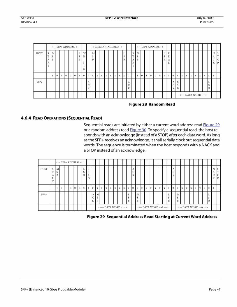
SFF-8431 SFP+ 2-wire Interface July 6, 2009
REVISION 4.1 PUBLISHED
Figure 28 Random Read
4.6.4 READ OPERATIONS (SEQUENTIAL READ)
Sequential reads are initiated by either a current word address read Figure 29 or a random address read Figure 30. To specify a sequential read, the host re-sponds with an acknowledge (instead of a STOP) after each data word. As long as the SFP+ receives an acknowledge, it shall serially clock out sequential data words. The sequence is terminated when the host responds with a NACK and
a STOP instead of an acknowledge.
Figure 29 Sequential Address Read Starting at Current Word Address
< -- SFP+ ADDRESS -> <- MEMORY ADDRESS -> < -- SFP+ ADDRESS -->
HOST START
MSB
LSB
WR I TE
MSB
LSB
START
MSB
LSB
READ
NACK
STOP
1 0 1 0 0 0 x 0 0 x x x x x x x x 0 1 0 1 0 0 0 x 1 0 x x x x x x x x 1
SFP+ ACK
ACK
ACK
MSB
LSB
<---- DATA WORD ---->
< -- SFP+ ADDRESS ->
HOST START
MSB
LSB
READ
ACK
ACK
NACK
STOP
1 0 1 0 0 0 x 1 0 x x x x x x x x 0 x x x x x x x x 0 x x x x x x x x 1
SFP+ ACK
MSB
LSB
MSB
LSB
MSB
LSB
<---- DATA WORD n --> <--- DATA WORD n+1 ---> <-- DATA WORD n+x -->
SFP+ (Enhanced 10 Gbps Pluggable Module) Page 47
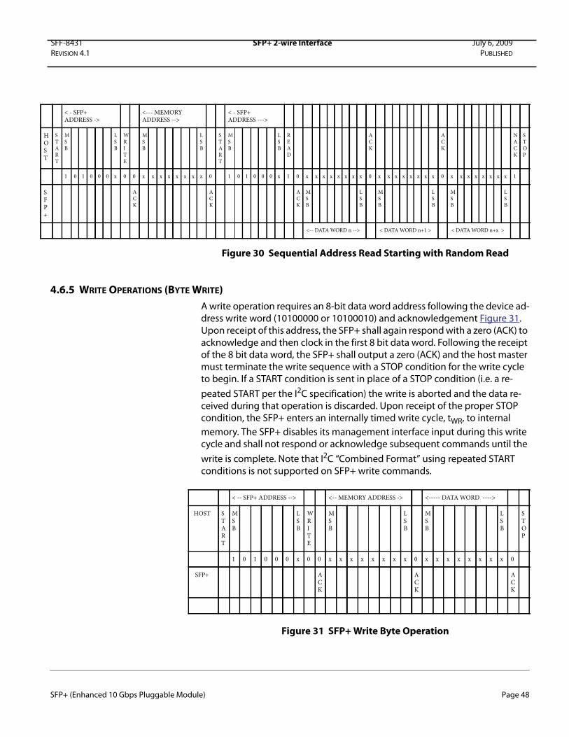
SFF-8431 SFP+ 2-wire Interface July 6, 2009
REVISION 4.1 PUBLISHED
Figure 30 Sequential Address Read Starting with Random Read
4.6.5 WRITE OPERATIONS (BYTE WRITE)
A write operation requires an 8-bit data word address following the device ad-dress write word (10100000 or 10100010) and acknowledgement Figure 31. Upon receipt of this address, the SFP+ shall again respond with a zero (ACK) to acknowledge and then clock in the first 8 bit data word. Following the receipt of the 8 bit data word, the SFP+ shall output a zero (ACK) and the host master must terminate the write sequence with a STOP condition for the write cycle to begin. If a START condition is sent in place of a STOP condition (i.e. a re-
peated START per the I2C specification) the write is aborted and the data re-ceived during that operation is discarded. Upon receipt of the proper STOP condition, the SFP+ enters an internally timed write cycle, tWR, to internal
memory. The SFP+ disables its management interface input during this write cycle and shall not respond or acknowledge subsequent commands until the
write is complete. Note that I2C “Combined Format” using repeated START conditions is not supported on SFP+ write commands.
Figure 31 SFP+ Write Byte Operation
< - SFP+ADDRESS ->
<--- MEMORY ADDRESS -->
< - SFP+ ADDRESS --->
HOST
START
MSB
LSB
WRITE
MSB
LSB
START
MSB
LSB
READ
ACK
ACK
NACK
STOP
1 0 1 0 0 0 x 0 0 x x x x x x x x 0 1 0 1 0 0 0 x 1 0 x x x x x x x x 0 x x x x x x x x 0 x x x x x x x x 1
SFP+
ACK
ACK
ACK
MSB
LSB
MSB
LSB
MSB
LSB
<-- DATA WORD n --> < DATA WORD n+1 > < DATA WORD n+x >
< -- SFP+ ADDRESS --> <-- MEMORY ADDRESS -> <----- DATA WORD ---->
HOST START
MSB
LSB
WRITE
MSB
LSB
MSB
LSB
STOP
1 0 1 0 0 0 x 0 0 x x x x x x x x 0 x x x x x x x x 0
SFP+ ACK
ACK
ACK
SFP+ (Enhanced 10 Gbps Pluggable Module) Page 48

SFF-8431 SFP+ 2-wire Interface July 6, 2009
REVISION 4.1 PUBLISHED
4.6.6 WRITE OPERATIONS (SEQUENTIAL WRITE)
SFP+ shall support up to an 8 sequential byte write without repeatedly sending SFP+ address and memory address information. A “sequential” write is initiated the same way as a single byte write, but the host master does not send a stop condition after the first word is clocked in. Instead, after the SFP+ acknowledges receipt of the first data word, the host can transmit up to seven more data words. The SFP+ shall send an acknowledge after each data word received. The host must terminate the sequential write sequence with a STOP condition or the write operation shall be aborted and data discarded. Note
that I2C “combined format” using repeated START conditions is not supported
on SFP+ write commands.
Figure 32 Sequential Write Operation
4.6.7 WRITE OPERATIONS (ACKNOWLEDGE POLLING)
Once the SFP+ internally timed write cycle has begun (and inputs are being ig-nored on the bus) acknowledge polling can be used to determine when the write operation is complete. This involves sending a START condition followed by the device address word. Only if the internal write cycle is complete shall the SFP+ respond with an acknowledge to subsequent commands, indicating read or write operations can continue.
< --- SFP+ ADDRESS --->
<--- MEMORY ADDRESS -->
<--DATA WORD 1 -->
<--- DATA WORD 2 --> <------ DATA WORD 3 ------>
<------ DATA WORD 4 ------>
HOST
START
MSB
LSB
WRITE
MSB
LSB
MSB
LSB
MSB
LSB
MSB
LSB
MSB
LSB
STOP
1 0 1 0 0 0 x 0 0 x x x x x x x x 0 x x x x x x x x 0 x x x x x x x x 0 x x x x x x x x 0 x x x x x x x x 0
SFP+
ACK
ACK
ACK
ACK
ACK
ACK
SFP+ (Enhanced 10 Gbps Pluggable Module) Page 49

SFF-8431 SFI Channel Recommendation (Informative) July 6, 2009
REVISION 4.1 PUBLISHED
APPENDIX A SFI CHANNEL RECOMMENDATION (INFORMATIVE)
A.1 SFI HOST CHANNEL GENERAL RECOMMENDATIONS
The purpose of the recommended SFI channel is to provide guidelines for host designers. The recommended SFI host channel consists of PCB traces, vias, and the 20 position enhanced connector defined by SFF-8083. The PCB traces are recommended to meet 100 ±10 Ω differential impedance with nominal 7% dif-ferential coupling.
SFI channel S-parameters are defined from ASIC transmitter pads to Host Com-pliance Board output at B and from Host Compliance Board input at C to ASIC input pads.
Please see SFF INF-8077i for differential S-parameters measurements and con-versions.
A.2 SFI CHANNEL TRANSFER RECOMMENDATIONS
The SFI maximum channel transfer budget is 9.0 dB allocated as shown in Table 25.
To mitigate multiple reflections, SFI also recommends a minimum channel at-tenuation. This requirement for both a minimum and maximum channel at-tenuation results in a mask that is shown approximately by Figure 33. The response including ripple should be within the channel response mask.
The SFI recommended channel is measured with the ASIC removed and mea-sured with the Host Compliance Board of section C.2. The S-parameters are measured by connecting a 4-port network analyzer to the ASIC pads and the SMA connectors on the Host Compliance Board.
Table 25 SFI Host Interconnect Budget
Parameter Symbol Conditions Min Max Units
Channel Transfer Including Connector measured
with Host Compliance Board (see Appendix C)
SDD21 at 5.5 GHz, see 1 -6.5 -2.25 dB
Penalty for reflections and other impairments -2.5 dB
Total Channel Link Budget When Measured with HCB -9.0 -2.25 dB
1.SFI channel response (SDD21) is defined from chip pads to compliance point B or C.
SFP+ (Enhanced 10 Gbps Pluggable Module) Page 50
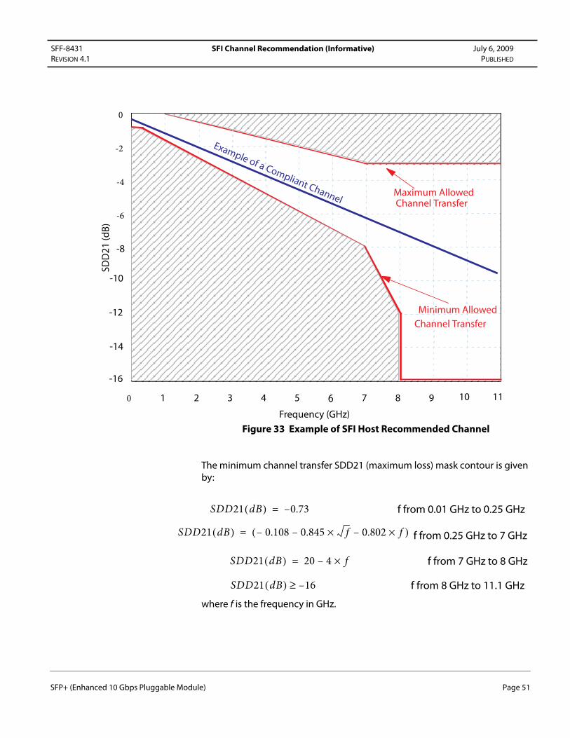
SFF-8431 SFI Channel Recommendation (Informative) July 6, 2009
REVISION 4.1 PUBLISHED
Figure 33 Example of SFI Host Recommended Channel
The minimum channel transfer SDD21 (maximum loss) mask contour is given by:
where f is the frequency in GHz.
SD
D2
1 (
dB
)
-6
-4
-2
0
-8
-10
Example of a Compliant Channel
Minimum Allowed
Channel Transfer
Frequency (GHz)
1 2 3 4 5 6 8 90 7 10 11
-16
-14
-12
Maximum Allowed Channel Transfer
SDD21 dB( ) 0.73–= f from 0.01 GHz to 0.25 GHz
SDD21 dB( ) 0.108– 0.845 f×– 0.802 f×–( )= f from 0.25 GHz to 7 GHz
SDD21 dB( ) 20 4 f×–= f from 7 GHz to 8 GHz
SDD21 dB( ) 16–≥ f from 8 GHz to 11.1 GHz
SFP+ (Enhanced 10 Gbps Pluggable Module) Page 51

SFF-8431 SFI Channel Recommendation (Informative) July 6, 2009
REVISION 4.1 PUBLISHED
The SFI channel maximum transfer is given by:.
where f is the frequency in GHz.
A.3 SFI CHANNEL RETURN LOSS RECOMMENDATIONS
The reflection coefficients, SDD11 and SDD22, of the SFI channel are recom-mended to meet the following equations:
where f is the frequency in GHz and SDDxx is either SDD11 or SDD22.
A.4 SFI CHANNEL RIPPLE RECOMMENDATIONS
SFI channel ripple is defined as the difference between the measured insertion response (SDD21m) and the fitted transfer response (SDD21f), all in dB magni-
tude:
The channel ripple magnitude should conform to the equation:
where the variable f (frequency) is in GHz. The above equation must be satis-fied over the frequency range of 0.25 GHz to 5.5 GHz.
SDD21 dB( ) 0= f from 0.25 GHz to 1.0 GHz
SDD21 dB( ) 0.5 1( f )–×= f from 1 GHz to 7 GHz
SDD21 dB( ) 3–= f from 7 GHz to 11.1 GHz
SDDxx dB( ) 14.5–≤ f from 0.01 to 5 GHz
SDDxx dB( ) 23.25– 8.75f
5---⎝ ⎠
⎛ ⎞×+≤ f from 5 to 11.1 GHz
Ripple dB( ) SDD21m SDD21 f–=
Ripple dB( ) 0.15 0.1 f×+≤
SFP+ (Enhanced 10 Gbps Pluggable Module) Page 52

SFF-8431 SFI Channel Recommendation (Informative) July 6, 2009
REVISION 4.1 PUBLISHED
SDD21m is the measured channel differential transfer response. SDD21f is the
fitted channel differential transfer response and is given by
Where a, b, and c are determined by the least squares fit over the frequency range of 250 MHz to 5.5 GHz as defined below. Frequency steps should be of equal size and not greater than 50 MHz.
Measured data will provide a frequency vector, f, and gain vector, G defined by
Create an input vector array called X from frequency variable f
Next calculate the coefficient vector using matrix math
Where the calculated coefficient values are given by
• a = -C(1)
• b = -C(2)
• c = -C(3).
SDD21 f a– b f×– c f ]×–[=
G 20 log10 SDD21[ ]×=
X
1 f 0 f 0
1 f 1 f 1
. . .
1 fn fn
=
C XT
X×[ ] XT
G×1–
=
SFP+ (Enhanced 10 Gbps Pluggable Module) Page 53

SFF-8431 SFI ASIC/SerDes Specification (Informative) July 6, 2009
REVISION 4.1 PUBLISHED
APPENDIX B SFI ASIC/SERDES SPECIFICATION (INFORMATIVE)
B.1 INTRODUCTION
SFI ASIC/SerDes specifications are informative. SFI ASIC/SerDes Transmitter specifications at reference point A are given in B.2. SFI ASIC/SerDes Receiver specifications at reference point D are given in B.3. ASIC/SerDes meeting the specifications in this appendix when used with the recommended channel of Appendix A are expected to meet the host specifications at B 3.5.1 and C 3.5.2, however any implementation that meets those host specifications is a com-pliant SFP+ implementation, independent of whether the ASIC/SerDes and/or channel meet the specifications in Appendix A and this appendix. This allows flexibility between channel and SerDes performances and costs.
B.2 SFI ASIC/SERDES TRANSMITTER OUTPUT SPECIFICATIONS AT A (INFORMATIVE)
The driver is based on low voltage high speed driver logic with a nominal dif-ferential impedance of 100 Ω. The SFI transmitter electrical specifications at reference point A are given in Table 26. The source must provide both differen-tial and common mode termination for quality signal termination and low EMI.
Pre-compensation such as de-emphasis may be required to mitigate data de-pendent jitter at compliance point B.
All parameters at A are measured with the ASIC/SerDes Test Board as shown in C.1.3.
Jitter specifications at A are not provided, the host transmitter in conjunction
with the host SFP+ channel must deliver jitter specifications as given by refer-
ence point B, Table 12.
B.3 SFI ASIC/SERDES RECEIVER INPUT SPECIFICATIONS AT D (INFORMATIVE)
SFI ASIC/SerDes receiver electrical specifications are given in Table 27 and measured at reference point D. All specifications at D are measured with the SerDes on a ASIC/SerDes Test Board C.1.3. The nominal receiver input imped-ance is 100 Ω differential. The load must provide differential termination and avoid significant differential to common mode conversion for high quality signal termination and low EMI.
The necessary jitter performance at D is to be determined by the implementer based on the specifications at C.
SFP+ (Enhanced 10 Gbps Pluggable Module) Page 54
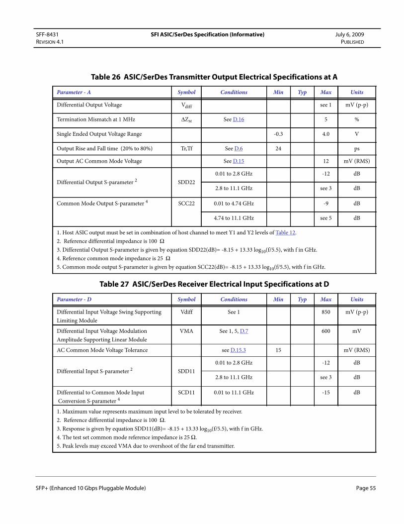
SFF-8431 SFI ASIC/SerDes Specification (Informative) July 6, 2009
REVISION 4.1 PUBLISHED
Table 26 ASIC/SerDes Transmitter Output Electrical Specifications at A
Parameter - A Symbol Conditions Min Typ Max Units
Differential Output Voltage Vdiff see 1 mV (p-p)
Termination Mismatch at 1 MHz ΔZM See D.16 5 %
Single Ended Output Voltage Range -0.3 4.0 V
Output Rise and Fall time (20% to 80%) Tr,Tf See D.6 24 ps
Output AC Common Mode Voltage See D.15 12 mV (RMS)
Differential Output S-parameter 2 SDD22
0.01 to 2.8 GHz -12 dB
2.8 to 11.1 GHz see 3 dB
Common Mode Output S-parameter 4 SCC22 0.01 to 4.74 GHz -9 dB
4.74 to 11.1 GHz see 5 dB
1. Host ASIC output must be set in combination of host channel to meet Y1 and Y2 levels of Table 12.
2. Reference differential impedance is 100 Ω3. Differential Output S-parameter is given by equation SDD22(dB)= -8.15 + 13.33 log10(f/5.5), with f in GHz.
4. Reference common mode impedance is 25 Ω5. Common mode output S-parameter is given by equation SCC22(dB)= -8.15 + 13.33 log10(f/5.5), with f in GHz.
Table 27 ASIC/SerDes Receiver Electrical Input Specifications at D
Parameter - D Symbol Conditions Min Typ Max Units
Differential Input Voltage Swing Supporting
Limiting Module
Vdiff See 1 850 mV (p-p)
Differential Input Voltage Modulation
Amplitude Supporting Linear Module
VMA See 1, 5, D.7 600 mV
AC Common Mode Voltage Tolerance see D.15.3 15 mV (RMS)
Differential Input S-parameter 2 SDD11
0.01 to 2.8 GHz -12 dB
2.8 to 11.1 GHz see 3 dB
Differential to Common Mode Input
Conversion S-parameter 4SCD11 0.01 to 11.1 GHz -15 dB
1. Maximum value represents maximum input level to be tolerated by receiver.
2. Reference differential impedance is 100 Ω.3. Response is given by equation SDD11(dB)= -8.15 + 13.33 log10(f/5.5), with f in GHz.
4. The test set common mode reference impedance is 25 Ω. 5. Peak levels may exceed VMA due to overshoot of the far end transmitter.
SFP+ (Enhanced 10 Gbps Pluggable Module) Page 55

SFF-8431 Application Reference Boards (Normative) July 6, 2009
REVISION 4.1 PUBLISHED
APPENDIX C APPLICATION REFERENCE BOARDS (NORMATIVE)
In order to provide test results that are reproducible and easily measured, this document defines 3 test boards that have SMA interfaces for easy connection to test equipment. One reference board is designed for testing the ASIC/SerDes, one reference board (HCB) for testing the host, and another ref-erence board (MCB) for testing the module. All host, module and ASIC/SerDes specifications and recommendations in this document, and the specifications for the mated pair of compliance boards, are defined at the SMA interfaces. This appendix describes these test cards in detail. The reference test boards’ objectives are:
• Satisfy the need for interoperablity at the electrical level.
• Allow for independent validation of ASIC/SerDes, host, and module.
• The PCB traces are targeted at 100 Ω differential impedance with nominal 7% differential coupling.
Testing compliance to specifications in a high-speed system is delicate and re-quires thorough consideration. Using common test boards that allow predict-able, repeatable and consistent results among vendors will help to ensure consistency and true compliance in the testing.
C.1 COMPLIANCE BOARDS
The Host Compliance Board, the Module Compliance Board, and the ASIC test board are made with defined losses of PCB trace with specific high perfor-mance properties. Compliance boards are intended to ease building practical test boards with non-zero loss. SFI specifications incorporate the effect of non-zero loss reference test boards which improve the return loss and slightly slows down edges.
Measurements made using non-compliant test boards are invalid and no valid conclusions can be drawn from the results.
C.1.1 HOST COMPLIANCE BOARD TRANSFER CHARACTERISTICS
SDD21 is defined from the SFF-8083 mating pads, excluding these mating pads, to the mating interface of the SMA connector. The Host Compliance Board is a passive test board and SDD21 and SDD12 should be identical. The recommended response of the Host Compliance Board PCB excluding the SFF-8083 connector is given by.
SDD21 dB( ) 0.01– 0.25 f×– 0.0916 f×–( )= from 0.01 to 15 GHz
SFP+ (Enhanced 10 Gbps Pluggable Module) Page 56

SFF-8431 Application Reference Boards (Normative) July 6, 2009
REVISION 4.1 PUBLISHED
where f is the frequency in GHz. From 10 MHz to 11.1 GHz the discrepancy be-tween the measured transfer response and the specified SDD21(dB) shall be <±15% of the transfer response in dB or ±0.1 dB, whichever is larger. For fre-quencies > 11.1 GHz and up to 15 GHz the discrepancy between measured transfer response and the specified SDD21(dB) shall be less than ±25% transfer response in dB.
The channel transfer characteristic is shown approximately in Figure 34.
Figure 34 Approximate Response of Host Compliance Board
SFF-8083 connector response is defined by SFF-8083.
C.1.2 MODULE COMPLIANCE BOARD TRANSFER CHARACTERISTICS
SDD21 is defined from the SFF-8083 connector, excluding its solder pads, to the mating interface of the SMA connector. The Host Compliance Board is a passive test board and SDD21 and SDD12 should be identical. The recom-mended response of the Module Compliance Board PCB excluding the SFF-8083 connector is given by:
where f is the frequency in GHz. Over the range of frequencies specified (10 MHz to 11.1 GHz) any discrepancy between measured transfer response and the specified SDD21(dB) shall be <±15% of the transfer response in dB or ±0.1 dB, whichever is larger. For frequencies > 11.1 GHz and up to 15 GHz the
Frequency (GHz)
1.5 3 4.5 6 7.5 9 12 13.5
SD
D2
1 (
dB
)
0
-1.5
-1
-0.5
0.0
-2
-2.5
10.5 15
SDD21 dB( ) 0.00045– 0.1135 f×– 0.04161 f×–( )= from 0.01 to 15 GHz
SFP+ (Enhanced 10 Gbps Pluggable Module) Page 57

SFF-8431 Application Reference Boards (Normative) July 6, 2009
REVISION 4.1 PUBLISHED
discrepancy between measured transfer response and the specified SDD21(dB) shall be less than ±25% of the transfer response in dB.
The channel transfer response is shown approximately in Figure 35.
Figure 35 Approximate Transfer Response of Module Compliance Board
SFP+ connector response is defined by SFF-8083.
C.1.3 ASIC/SERDES TEST BOARD TRANSFER CHARACTERISTICS
The recommended response of the ASIC/SerDes test board PCB is the same as for the Module Compliance Board (see C.1.2).
Frequency (GHz)
1.5 3 4.5 6 7.5 9 12 13.5
SD
D2
1 (
dB
)
0
-0.75
-0.5
-0.25
0.0
-1
-1.25
10.5 15
SFP+ (Enhanced 10 Gbps Pluggable Module) Page 58
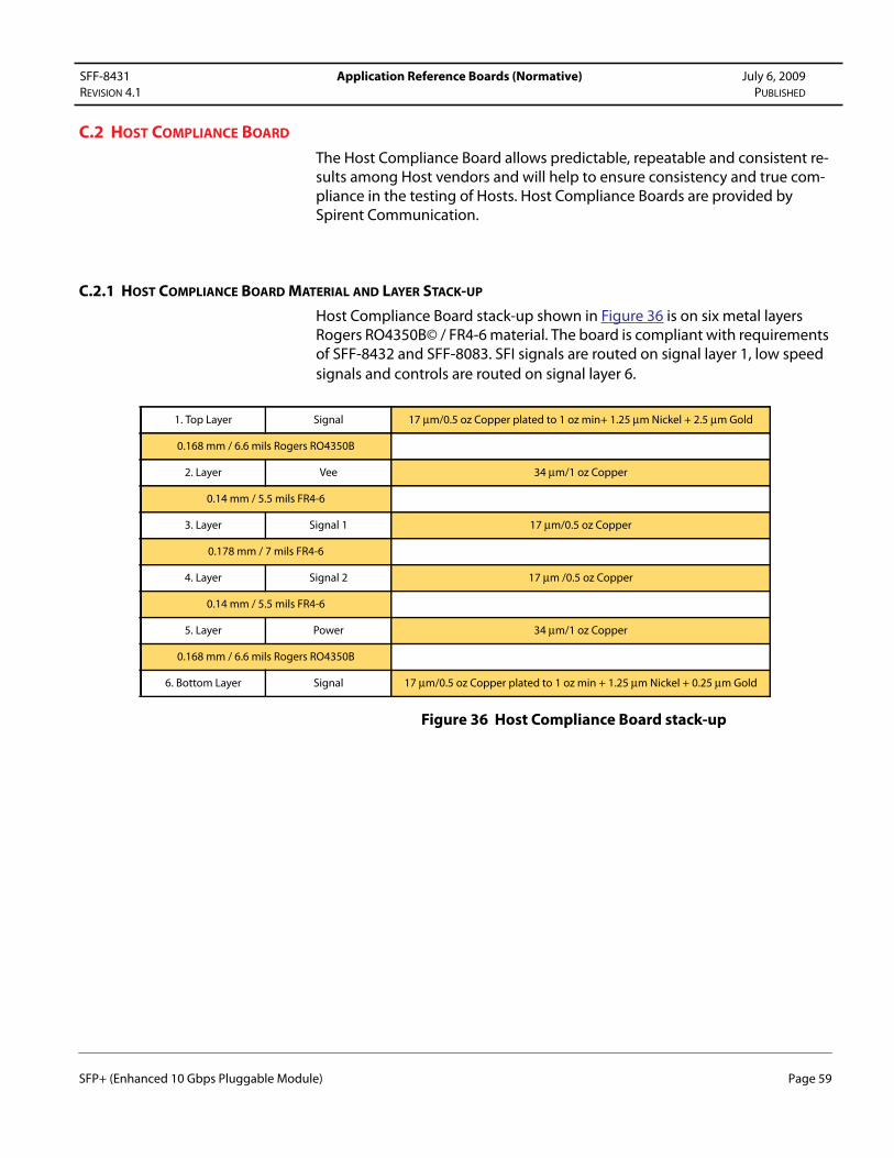
SFF-8431 Application Reference Boards (Normative) July 6, 2009
REVISION 4.1 PUBLISHED
C.2 HOST COMPLIANCE BOARD
The Host Compliance Board allows predictable, repeatable and consistent re-sults among Host vendors and will help to ensure consistency and true com-pliance in the testing of Hosts. Host Compliance Boards are provided by Spirent Communication.
C.2.1 HOST COMPLIANCE BOARD MATERIAL AND LAYER STACK-UP
Host Compliance Board stack-up shown in Figure 36 is on six metal layers Rogers RO4350B© / FR4-6 material. The board is compliant with requirements of SFF-8432 and SFF-8083. SFI signals are routed on signal layer 1, low speed
signals and controls are routed on signal layer 6.
Figure 36 Host Compliance Board stack-up
1. Top Layer Signal 17 μm/0.5 oz Copper plated to 1 oz min+ 1.25 μm Nickel + 2.5 μm Gold
0.168 mm / 6.6 mils Rogers RO4350B
2. Layer Vee 34 μm/1 oz Copper
0.14 mm / 5.5 mils FR4-6
3. Layer Signal 1 17 μm/0.5 oz Copper
0.178 mm / 7 mils FR4-6
4. Layer Signal 2 17 μm /0.5 oz Copper
0.14 mm / 5.5 mils FR4-6
5. Layer Power 34 μm/1 oz Copper
0.168 mm / 6.6 mils Rogers RO4350B
6. Bottom Layer Signal 17 μm/0.5 oz Copper plated to 1 oz min + 1.25 μm Nickel + 0.25 μm Gold
SFP+ (Enhanced 10 Gbps Pluggable Module) Page 59

SFF-8431 Application Reference Boards (Normative) July 6, 2009
REVISION 4.1 PUBLISHED
C.2.2 HOST COMPLIANCE BOARD PARTLIST
The Host Compliance Board part list is given below.
Note: Table 28 does not use all in-sequence part numbers.
C.2.3 HCB GERBER FILES
The Gerber file for the Host Compliance Board is available in SFF-8434.
C.2.4 SCHEMATIC OF HOST COMPLIANCE BOARD
The schematic of Host Compliance Board is shown in Figure 37.
Mod-DEF0 in the schematic is Mod_ABS as defined by Table 3 and AS0/AS1 in the schematic are RS0/RS1 as defined by Table 3.
Table 28 Host Compliance Board Part List
Qty RefDes Value Description Example Part Number
2 C5, C6 0.1 uF Ceramic Capacitor 10% X7R 10V 0402 SMT LFR
3 D1, D2, D3 GREEN LED Single Green 120 DEG 0603 SMT LFR
2 D4, D5 Blue LED Single Blue 120 DEG 0603 SMT LFR
1 J1 Conn3 Connector Header 3 Pins Straight Tyco PN#3-644695-3
4 J2, J3, J4, J5 EDGE SMA SMA Connector Jack R/A Rosenberger PN# 32K243-40ME3
1 J6 CONN1X3P Connector Header 3 Pins 100 mil Pitch Molex PN# 22-23-203
5 R1, R2, R3, R4, R5 1.0 kΩ Resistor RES 1.00K 1% 1/10W 0603 SMT LFR
1 SW1 SPST SW 4 Position Dip Switch SMT ITT Cannon PN# TDA04H0SB1
SFP+ (Enhanced 10 Gbps Pluggable Module) Page 60
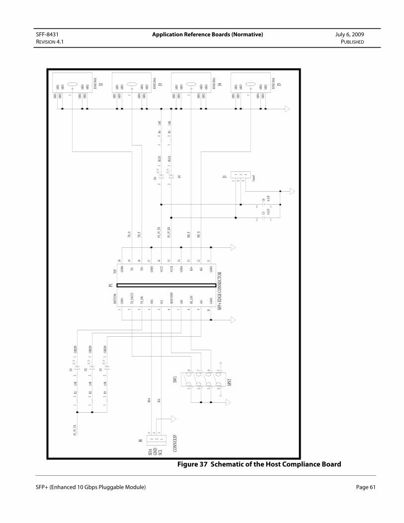
SFF-8431 Application Reference Boards (Normative) July 6, 2009
REVISION 4.1 PUBLISHED
Figure 37 Schematic of the Host Compliance Board
J1
Conn
311
22
33
R31.0
K1
2
SW1
SPST
18
2 3
7 6
45
D5
BLU
E2
1
J5
EDGE
SMA
MH
1M
H1
11
MH
2M
H2
MH
3M
H3
MH
4M
H4
R41.0
K1
2
C6 0.1U
F
12
R51.0
K1
2
C5 0.1U
F
12
P1
TX_F
AULT
2
GND
11
TX_D
IS3
SDA
4
SCL
5
MO
D-D
EF0
6
AS0
7
RX_L
OS
8
AS1
9
GND
210
GND
620
TD-
19
TD+
18
GND
517
VCCT
16
VCCR
15
GND
414
RD+
13
RD-
12
GND
311
BOTT
OM
TOP
D1
GREE
N2
1
J2
EDGE
SMA
MH
1M
H1
11
MH
2M
H2
MH
3M
H3
MH
4M
H4
J6
CON
N1X
3P11
22
33
D2
GREE
N2
1
R11.0
K1
2
J3
EDGE
SMA
MH
1M
H1
11
MH
2M
H2
MH
3M
H3
MH
4M
H4
D3
GREE
N2
1
D4
BLU
E2
1
R21.0
K1
2
J4
EDGE
SMA
MH
1M
H1
11
MH
2M
H2
MH
3M
H3
MH
4M
H4
RD_N
RD_P
TD_N
TD_P
SCL
SDA
P3_3
V_RX
P3_3
V_TX
P3_3
V_TX
SFP+
ED
GE C
ON
NEC
TOR
SCL
SDA
GND
SFP+ (Enhanced 10 Gbps Pluggable Module) Page 61
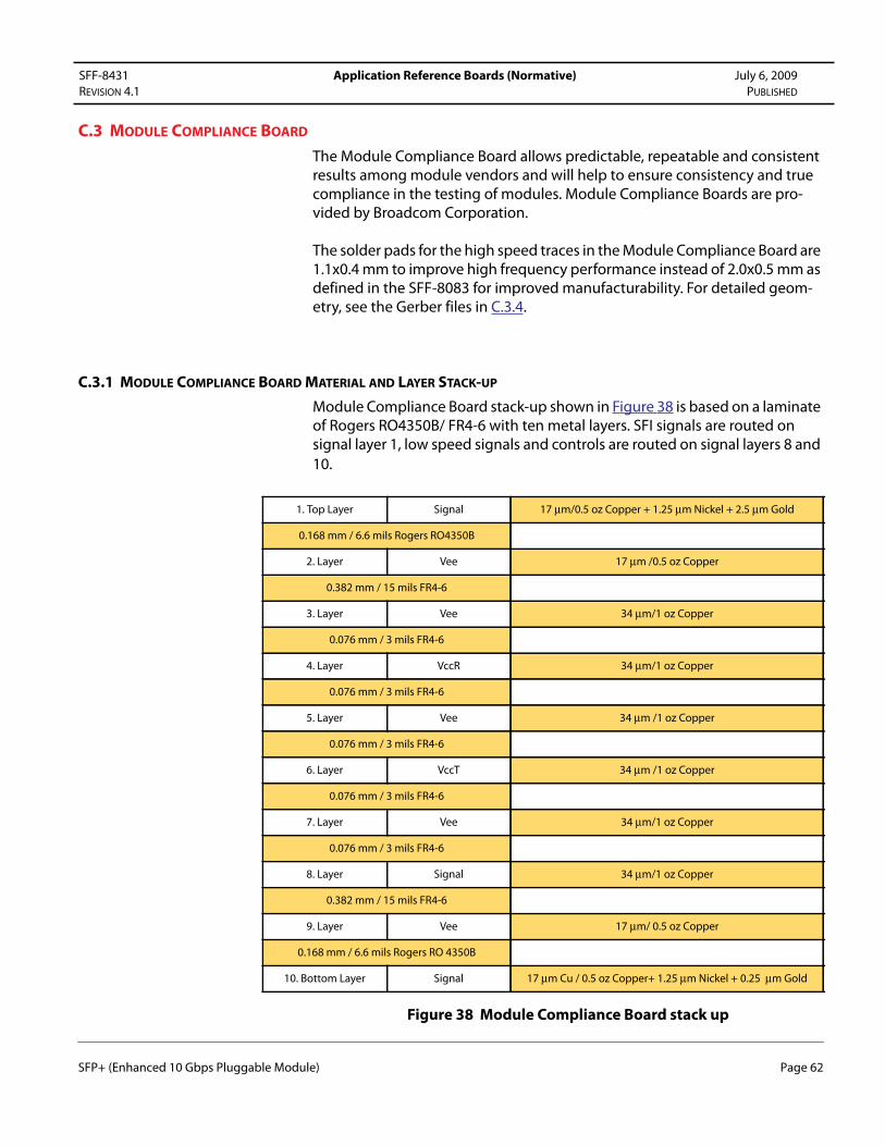
SFF-8431 Application Reference Boards (Normative) July 6, 2009
REVISION 4.1 PUBLISHED
C.3 MODULE COMPLIANCE BOARD
The Module Compliance Board allows predictable, repeatable and consistent results among module vendors and will help to ensure consistency and true compliance in the testing of modules. Module Compliance Boards are pro-vided by Broadcom Corporation.
The solder pads for the high speed traces in the Module Compliance Board are 1.1x0.4 mm to improve high frequency performance instead of 2.0x0.5 mm as defined in the SFF-8083 for improved manufacturability. For detailed geom-etry, see the Gerber files in C.3.4.
C.3.1 MODULE COMPLIANCE BOARD MATERIAL AND LAYER STACK-UP
Module Compliance Board stack-up shown in Figure 38 is based on a laminate of Rogers RO4350B/ FR4-6 with ten metal layers. SFI signals are routed on signal layer 1, low speed signals and controls are routed on signal layers 8 and
10.
Figure 38 Module Compliance Board stack up
1. Top Layer Signal 17 μm/0.5 oz Copper + 1.25 μm Nickel + 2.5 μm Gold
0.168 mm / 6.6 mils Rogers RO4350B
2. Layer Vee 17 μm /0.5 oz Copper
0.382 mm / 15 mils FR4-6
3. Layer Vee 34 μm/1 oz Copper
0.076 mm / 3 mils FR4-6
4. Layer VccR 34 μm/1 oz Copper
0.076 mm / 3 mils FR4-6
5. Layer Vee 34 μm /1 oz Copper
0.076 mm / 3 mils FR4-6
6. Layer VccT 34 μm /1 oz Copper
0.076 mm / 3 mils FR4-6
7. Layer Vee 34 μm/1 oz Copper
0.076 mm / 3 mils FR4-6
8. Layer Signal 34 μm/1 oz Copper
0.382 mm / 15 mils FR4-6
9. Layer Vee 17 μm/ 0.5 oz Copper
0.168 mm / 6.6 mils Rogers RO 4350B
10. Bottom Layer Signal 17 μm Cu / 0.5 oz Copper+ 1.25 μm Nickel + 0.25 μm Gold
SFP+ (Enhanced 10 Gbps Pluggable Module) Page 62

SFF-8431 Application Reference Boards (Normative) July 6, 2009
REVISION 4.1 PUBLISHED
C.3.2 SCHEMATIC OF MODULE COMPLIANCE BOARD
Schematic of Module Compliance Board is shown in Figure 39.
Mod-DEF0 in the schematic is Mod_ABS as defined by Table 3 and AS0/AS1 in the schematic are RS0/RS1 as defined by Table 3.
SFP+ (Enhanced 10 Gbps Pluggable Module) Page 63
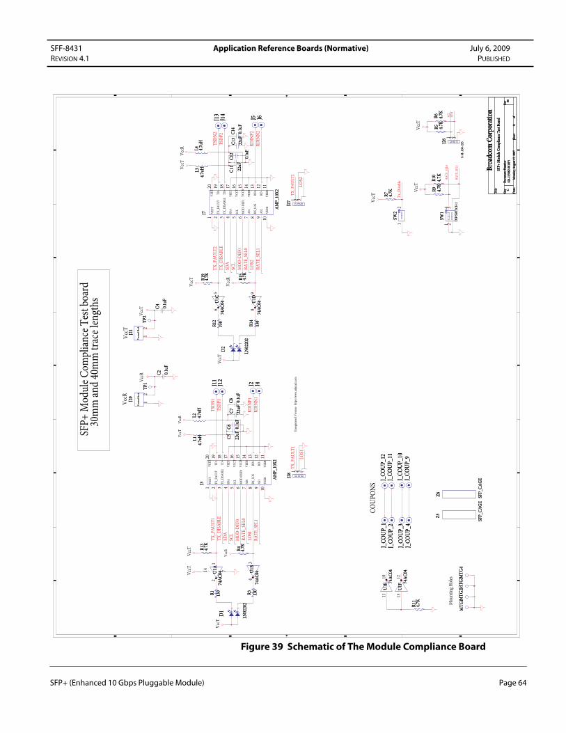
SFF-8431 Application Reference Boards (Normative) July 6, 2009
REVISION 4.1 PUBLISHED
Figure 39 Schematic of The Module Compliance Board
Unr
egis
tere
d V
ersi
on -
htt
p://
ww
w.a
idec
ad.c
om
5 5
4 4
3 3
2 2
1 1
DD
CC
BB
AA
RD
INP
1
TSD
P1
RA
TE
_SE
L1
TX
_DIS
AB
LE
TSD
N1
MO
D-D
EF0
RA
TE
_SE
L1
RA
TE
_SE
L0
SDA
RD
INN
1
SCL
RA
TE
_SE
L1
RA
TE
_SE
L0
SDA
TX
_FA
ULT
2
TX
_DIS
AB
LE
SCL
MO
D-D
EF0
RD
INN
2
RD
INP
2LO
S2
TSD
P2
TSD
N2
LOS1
TX
_FA
ULT
1
RA
TE
_SE
L0
SDA
Tx_
Dis
able
SCL
TX
_FA
ULT
2
LOS2
TX
_FA
ULT
1
LOS1
Vcc
T
Vcc
R
Vcc
TV
ccT
Vcc
TV
ccR
Vcc
R
Vcc
TV
ccR
Vcc
T
Vcc
T
Vcc
R
Vcc
T
Vcc
TV
ccT
Vcc
T
Tit
le
Size
Doc
umen
t Num
ber
Rev
Dat
e:Sh
eet
of
824-
1158
82-0
010P
100
SFP
+ M
odul
e C
ompl
ian
ce T
est B
oard
C
11M
onda
y, A
ugus
t 27,
200
7
Bro
adco
m C
orpo
rati
onT
itle
Size
Doc
umen
t Num
ber
Rev
Dat
e:Sh
eet
of
824-
1158
82-0
010P
100
SFP
+ M
odul
e C
ompl
ian
ce T
est B
oard
C
11M
onda
y, A
ugus
t 27,
200
7
Bro
adco
m C
orpo
rati
onT
itle
Size
Doc
umen
t Num
ber
Rev
Dat
e:Sh
eet
of
824-
1158
82-0
010P
100
SFP
+ M
odul
e C
ompl
ian
ce T
est B
oard
C
11M
onda
y, A
ugus
t 27,
200
7
Bro
adco
m C
orpo
rati
on
SFP
+ M
odul
e C
ompl
ianc
e T
est b
oard
3
0mm
and
40m
m tr
ace
leng
ths
Vcc
RV
ccT
VE
ET
TX
_DIS
AB
LE
TX
_FA
ULT
SDA
SCL
MO
D-D
EF0
AS0
RX
_LO
S
AS1
VE
ER
VE
ER
RD
+
VE
ER
VC
CR
VC
CT
VE
ET
TD
+
TD
-
VE
ET
RD
-
CO
UP
ON
S
Mou
ntin
g H
oles
RD
-
VE
ET
TX
_DIS
AB
LE
TX
_FA
ULT
SDA
SCL
MO
D-D
EF1
RX
_LO
S
AS1
AS2
VE
ER
VE
ER
RD
+
VC
CT
VC
CR
VE
ER
TD
+
VE
ET
VE
ET
TD
-
D2
LN02
202
D2
LN02
202
U1D
74A
C04U
1D74
AC
04
98
J3
AM
P_1
0X2
J3
AM
P_1
0X2
1 2 3 4 5 6 7 8 9 1011121314151617181920
R15
4.7K
R15
4.7K
L14.
7uH
L14.
7uH
R3
130
R3
130
U1C
74A
C04U
1C74
AC
04
56
J_C
OU
P_9
J_C
OU
P_9
J_C
OU
P_1
1J_
CO
UP
_11
MT
G3
MT
G3
C4
0.1u
F
C4
0.1u
F
R4
4.7K
R4
4.7K
ON
SW1
DIP
-SW
ITC
H-2
ON
SW1
DIP
-SW
ITC
H-2
1 234
J4J4U
1B74
AC
04U1B
74A
C04
34
R9
4.7K
R9
4.7K
C8
0.1u
F
C8
0.1u
F
J_C
OU
P_3
J_C
OU
P_3
Z5
SFP
_CA
GE
Z5
SFP
_CA
GE
MT
G2
MT
G2
U1A
74A
C04U
1A74
AC
04
12
14 7
ON
SW2 O
NSW
21
2
J28
J28 1 2 3
C13
22uF
C13
22uF
R19
4.7K
R19
4.7K
TP
2T
P2
C5
22uF
C5
22uF
MT
G4
MT
G4
R5
4.7K
R5
4.7K
R1
130
R1
130
J21
Ter
min
al B
lock
J21
Ter
min
al B
lock
12
C14 0.1u
F
C14 0.1u
F
Z6
SFP
_CA
GE
Z6
SFP
_CA
GE
MT
G1
MT
G1
R14
130
R14
130
R6
4.7K
R6
4.7K
TP
1T
P1 J2J2
R10
4.7K
R10
4.7K
C11 22
uF
C11 22
uF
R12
130
R12
130
J12
J12
R13
4.7K
R13
4.7K
J14
J14
J6J6J5J5
C6
0.1u
F
C6
0.1u
F
J13
J13
J11
J11
J_C
OU
P_4
J_C
OU
P_4
J_C
OU
P_1
J_C
OU
P_1
J_C
OU
P_1
0J_
CO
UP
_10
J27
J27 1 2 3
C12 0.1u
F
C12 0.1u
F
C7
22uF
C7
22uF
J26
S-M
-.10
0-1X
3J26
S-M
-.10
0-1X
3
1 2 3
R7
4.7K
R7
4.7K
L34.
7uHL3
4.7u
H
U1F
74A
C04
U1F
74A
C04
1312
R11
4.7K
R11
4.7K
C2 0.1u
F
C2 0.1u
F
J20
Ter
min
al B
lock
J20
Ter
min
al B
lock
12
L2 4.7u
HL2 4.
7uH
L4 4.7u
HL4 4.
7uH
J_C
OU
P_2
J_C
OU
P_2
J7
AM
P_1
0X2
J7
AM
P_1
0X2
1 2 3 4 5 6 7 8 9 1011121314151617181920
U1E
74A
C04
U1E
74A
C04
1110
J_C
OU
P_1
2J_
CO
UP
_12
D1
LN02
202
D1
LN02
202
SFP+ (Enhanced 10 Gbps Pluggable Module) Page 64

SFF-8431 Application Reference Boards (Normative) July 6, 2009
REVISION 4.1 PUBLISHED
C.3.3 MODULE COMPLIANCE BOARD PARTLIST
Component part list for the Module Compliance Board is given below.
Note: Table 29 does not use all in-sequence part numbers.
C.3.4 MCB GERBER FILES
The Gerber file for the Module Compliance Board is available in SFF-8434.
Table 29 Module Compliance Board Part List
Qty RefDes Value Description Example Part Numbers
6 C2, C4, C6, C8, C12, C14 0.1uF Ceramic Capacitors Murata/GRM188R71C104MA01D
4 C5, C7, C11, C13 22 uF Ceramic Capacitors Murata/GRM21BR60J226ME39K
4 D1, D2, D4, D5 RED LED Panasonic/LNJ208R8ARA
12 J_COUP_2, J2, J_COUP_4, J4, J5,J6,
J_COUP_9, J_COUP_11, J12,
J14J_COUP_1, J_COUP_3,
J_COUP_10, J11, J_COUP_12, J13
SMA SMA Connector R/A Huber&Suhner/92_SK-U50-0-
3/199_NE
2 J3, J7 Con_10x2 SFF-8083 Connector Tyco 1888247 or Molex 74441
2 J20, J21 Terminal Block Terminal Bloc On-Shore-Tech/EDZ5002DS
3 J26, J27, J28 S-M-.100-1X3 PCB Header Molex/22-10-2031
4 L1, L2, L3, L4 4.7 uH Inductor Toko/A914BYW-4R7M
4 R1, R3, R12, R14 130 Ω Resistors Walsin/WR06X131JTL
10 R4, R5, R6, R7, R9, R10, R11, R13,
R15, R19
4.7 kΩ Resistors Walsin/WR06X472JTL
1 SW1 DIP-SWITCH-2 DipSwitch CT2062-ND
1 SW2 sw_pb_ck-k Toggle Switch C&K/ET01MD1AVBE
1 U1 74AC04 Inverter Fairchild/530438-00
2 Z5, Z6 SFP_CAGE SFP Cage Tyco 1489962-1
SFP+ (Enhanced 10 Gbps Pluggable Module) Page 65
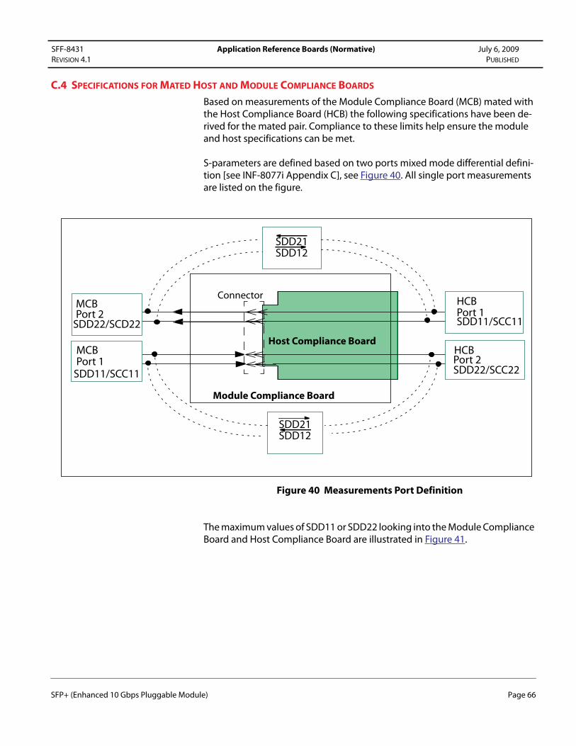
SFF-8431 Application Reference Boards (Normative) July 6, 2009
REVISION 4.1 PUBLISHED
C.4 SPECIFICATIONS FOR MATED HOST AND MODULE COMPLIANCE BOARDS
Based on measurements of the Module Compliance Board (MCB) mated with the Host Compliance Board (HCB) the following specifications have been de-rived for the mated pair. Compliance to these limits help ensure the module and host specifications can be met.
S-parameters are defined based on two ports mixed mode differential defini-tion [see INF-8077i Appendix C], see Figure 40. All single port measurements are listed on the figure.
Figure 40 Measurements Port Definition
The maximum values of SDD11 or SDD22 looking into the Module Compliance Board and Host Compliance Board are illustrated in Figure 41.
Module Compliance Board
Connector
Host Compliance Board
HCB
MCB HCB
SDD11/SCC11
SDD11/SCC11 SDD22/SCC22
Port 1
Port 2Port 1
MCB
SDD22/SCD22 Port 2
SDD21SDD12
SDD21SDD12
SFP+ (Enhanced 10 Gbps Pluggable Module) Page 66

SFF-8431 Application Reference Boards (Normative) July 6, 2009
REVISION 4.1 PUBLISHED
Figure 41 Maximum Differential Response of mated MCB and HCB
The maximum values of SDD11 or SDD22 looking into the Module Compliance Board are given by the following equations:
SDDxx dB( ) 20– 2.75 f×+≤ f in GHz from 0.01 to 2
SDDxx dB( ) 14.5–≤ f in GHz from 2 to 5
SDDxx dB( ) 23.25– 8.75f
5---⎝ ⎠
⎛ ⎞×+≤ f in GHz from 5 to 11.1
SFP+ (Enhanced 10 Gbps Pluggable Module) Page 67

SFF-8431 Application Reference Boards (Normative) July 6, 2009
REVISION 4.1 PUBLISHED
The maximum values of SDD11 or SDD22 looking into the Host Compliance Board are given by the following equations:
The maximum and the minimum values of SDD21 or SDD12 looking into ei-ther the Module Compliance Board or Host Compliance Board are illustrated in Figure 42 and given by the equations below.
Figure 42 Mated MCB-HCB Differential Through Response Limits
SDDxx dB( ) 20– 2 f×+≤ f in GHz from 0.01 to 2.5
SDDxx dB( ) 15–≤ f in GHz from 2.5 to 5
SDDxx dB( ) 13.8– 28.85f
5.5------⎝ ⎠
⎛ ⎞10
log×+≤f in GHz from 5 to 11.1
SDDxx dB( ) 0.012– 0.694 f×– 0.127 f×–( )≤ f in GHz from 0.01 to 5.5
SDDxx dB( ) 0.75 0.65 f×–≤ f in GHz from 5.5 to 11.1
SDDxx dB( ) 0.0915 0.549 f×– 0.101 f×–≤ f in GHz from 0.01 to 11.1
SFP+ (Enhanced 10 Gbps Pluggable Module) Page 68

SFF-8431 Application Reference Boards (Normative) July 6, 2009
REVISION 4.1 PUBLISHED
The maximum values of SCC11 or SCC22 looking into either the Module Com-pliance Board or Host Compliance Board are illustrated in Figure 43.
Figure 43 Maximum Common Mode Response of mated MCB and HCB
The SCC11 and SCC22 are also given by the following equations:
SCCxx dB( ) 12– 2.8 f×+≤ f in GHz from 0.01 to 2.5
SCCxx dB( ) 5.2– 0.08 f×+≤ f in GHz from 2.5 to 15.
SFP+ (Enhanced 10 Gbps Pluggable Module) Page 69

SFF-8431 Application Reference Boards (Normative) July 6, 2009
REVISION 4.1 PUBLISHED
The maximum values of Differential to Common Mode Response SCD21 and SCD12 looking into either the Module Compliance Board or Host Compliance Board are illustrated in Figure 44.
Figure 44 Maximum Differential to Common Mode Response of mated MCB and HCB
Mated response SCD21 and SCD12 of the mated Module and Host Compliance Board are given by:
When MCB Port 1 of the mated Module Compliance Board and Host Compli-ance Board is excited by the crosstalk source defined in Table 12, the RMS dif-ferential NEXT voltage at MCB Port 2 shall be less than 1 mV when measured in a 12 GHz bandwidth. The differential NEXT voltage from HCB Port 1 to HCB Port 2 is expected to be about the same. Compliance boards meeting this re-sponse are expected to pass the integrated NEXT requirement, however it is also expected that the curve can be exceeded due to frequency resonances while still passing the integrated NEXT requirement. The frequency domain curve shown in Figure 45 shows a recommended response which is described in the equations following the figure. Compliance boards meeting this NEXT response are expected to pass the NEXT voltage requirement, however it is
SCDxx dB( ) 30– 2.91 f×+≤ f in GHz from 0.01 to 5.5
SCDxx dB( ) 14–≤ f in GHz from 5.5 to 15.
SFP+ (Enhanced 10 Gbps Pluggable Module) Page 70

SFF-8431 Application Reference Boards (Normative) July 6, 2009
REVISION 4.1 PUBLISHED
also expected that the curve can be exceeded due to frequency resonances while still passing the NEXT voltage requirement.
Figure 45 Maximum Differential NEXT Response of mated MCB and HCB
The recommended NEXT response is also given by the following equations:
NEXT dB( ) 50–≤ f in GHz from 0.01 to 4
NEXT dB( ) 70– 5 f×+≤ f in GHz from 4 to 8
NEXT dB( ) 30–≤ f in GHz from 8 to 15.
SFP+ (Enhanced 10 Gbps Pluggable Module) Page 71

SFF-8431 Test Methodology and Measurement (Normative) July 6, 2009
REVISION 4.1 PUBLISHED
APPENDIX D TEST METHODOLOGY AND MEASUREMENT (NORMATIVE)
D.1 INTRODUCTION
This appendix defines metrics for SFP+ high-speed and power electrical inter-faces and provides practical guidance for test implementation. Each param-eter is defined in terms of a measurement procedure. The instruments for measurement are assumed to be ideal: accurate, precise, with infinite or de-fined bandwidth, zero or defined noise and so on. In practice, the necessary level of instrument performance and the approach to calibration and mar-gining must be considered. Some guidance is given in the following sections.
All measurements are made differentially, with the exception of AC Common Mode Generation Test D.15.2, Common Mode Tolerance Test D.15.3, Termina-tion Mismatch D.16, Module Power Supply Tolerance Filtering D.17, and Power Supply Noise Testing Methodology D.17.
Accurate calibration of test equipment is assumed for all measurements. To avoid pessimistic WDP and jitter results, the scope may require correction for time base linearity errors.
D.1.1 TEST PATTERNS
Test patterns used in this specification include the 8+8 square wave, PRBS9, IEEE 802.3 test patterns1, 2 and 3, and any valid 64B/66B signal. PRBS9 is de-fined in IEEE Std 802.3, 68.6.1 and a file for the sequence can be found at http://ieee802.org/3/aq/public/tools/TWDP/prbs9_950.txt. Test patterns 1, 2 and 3 are defined in IEEE Std 802.3, 52.9.1.1. Test pattern 3 is PRBS31 as defined by ITU-T or in IEEE Std 802.3, 49.2.8.
D.2 EYE MASK COMPLIANCE
This section defines what is meant by eye mask compliance and gives guid-ance for its determination. Mask templates and coordinates are given in sub-clauses in 3.5 SFP+ Host System Specifications and 3.6 SFP+ Module Specifications .
• The pattern(s) for eye mask testing is according to the relevant stan-dard(s) listed in Table 1.
SFP+ (Enhanced 10 Gbps Pluggable Module) Page 72

SFF-8431 Test Methodology and Measurement (Normative) July 6, 2009
REVISION 4.1 PUBLISHED
• The output being tested should comply over the range of operating con-ditions while the opposing direction bit stream, operates with the target crosstalk rise and fall and amplitude given in Table 12, Table 14, Table 17, and Table 18. The opposing direction bit stream (than the one being test-ed) shall be asynchronous PRBS31 or valid 64B/66B bit stream.
Testing may include guard banding, extrapolation, or other methods, but must ensure that mask violations do not occur at a rate exceeding the hit ratio limit given in the appropriate table.
• An AC coupling 3 dB corner frequency of 20 kHz is expected to be ade-quate to eliminate baseline wander effects, however high frequency per-formance is critical and must not be sacrificed by the AC coupling.
• All loads are specified at 100 Ω differential.
• 0.0 UI and 1.0 UI on the time axis are defined by the eye crossing means at the average value (zero volts if AC coupled) of the signal. The average val-ue might not be at the jitter waist.
A clock recovery unit (CRU) is used to trigger the scope for mask measure-ments as shown in Figure 46. The reference CRU has a high frequency corner bandwidth of 4 MHz and a slope of -20 dB/decade with peaking of 0.1 dB or less.
Figure 46 Eye mask measurement setup - block diagram.
D.2.1 EXAMPLE CALCULATIONS FOR 5X10⁻⁵ HIT RATIO
If an oscilloscope records 1350 samples/screen, and the time-base is set to 0.2 UI per division with 10 divisions across the screen, and the measurement is continued for 200 waveforms, then a transmitter with repeated measurement averaging to less than 6.75 hits is compliant. i.e.,
Likewise, if a measurement is continued for 1000 waveforms, then repeated measurement averaging to less than 33.75 hits is compliant. An extended measurement is expected to give a more repeatable result, whereas a single reading of 6 hits in 200 waveforms would not give a statistically significant pass or fail.
DUT
CRU
Trigger
+Data
- Data
OscilloscopeDCBlock
DCBlock
Hit Ratio5 10
5–× 1350×0.2 10×
----------------------------------- 6.75==
SFP+ (Enhanced 10 Gbps Pluggable Module) Page 73

SFF-8431 Test Methodology and Measurement (Normative) July 6, 2009
REVISION 4.1 PUBLISHED
D.3 DATA DEPENDENT JITTER (DDJ) AND PULSE WIDTH SHRINKAGE (DDPWS)
A high-resolution oscilloscope, time interval analyzer, or other instrument with equivalent capability may be used to measure DDJ and DDPWS. A repeating PRBS9 pseudo-random test pattern, 511 bits long, is used. For electrical jitter measurements, the measurement bandwidth is 12 GHz. If the measurement bandwidth affects the result, it can be corrected for by post-processing. How-ever, a bandwidth above 12 GHz is expected to have little effect on the results.
DCD and Pulse Width Shrinkage (DDPWS) are components of DDJ.
Establish a crossing level equal to the average value of the entire waveform being measured. Synchronize the instrument to the pattern repetition fre-quency and average the waveforms or the crossing times sufficiently to re-move the effects of random jitter and noise in the system. The PRBS9 pattern has 128 positive-going transitions and 128 negative-going transitions. The mean time of each crossing is then compared to the expected time of the crossing, and a set of 256 timing variations is determined. DDJ is the range (max-min) of the timing variations. Keep track of the signs (early/late) of the variations. Note, it may be convenient to align the expected time of one of the crossings with the measured mean crossing.
The following Figure 47 illustrates the method. The vertical axis is in arbitrary units, and the horizontal axis is plotted in UI. The waveform is AC coupled to an average value of 0, therefore 0 is the appropriate crossing level. The rectan-gular waveform shows the ideal crossing times, and the other is the waveform with jitter that is being measured. Only 32 UI are shown (out of 511). The wave-forms have been arbitrarily aligned with (Δt2 = 0) at 14 UI.
Figure 47 DDJ Test Method
t1 t2 t3
Δt2=0
....etc.
SFP+ (Enhanced 10 Gbps Pluggable Module) Page 74
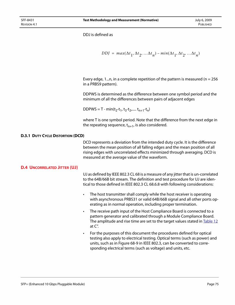
SFF-8431 Test Methodology and Measurement (Normative) July 6, 2009
REVISION 4.1 PUBLISHED
DDJ is defined as
Every edge, 1...n, in a complete repetition of the pattern is measured (n = 256 in a PRBS9 pattern).
DDPWS is determined as the difference between one symbol period and the minimum of all the differences between pairs of adjacent edges
DDPWS = T - min(t2-t1, t3-t2,..... tn+1-tn)
where T is one symbol period. Note that the difference from the next edge in the repeating sequence, tn+1, is also considered.
D.3.1 DUTY CYCLE DISTORTION (DCD)
DCD represents a deviation from the intended duty cycle. It is the difference between the mean position of all falling edges and the mean position of all rising edges with uncorrelated effects minimized through averaging. DCD is measured at the average value of the waveform.
D.4 UNCORRELATED JITTER (UJ)
UJ as defined by IEEE 802.3 CL 68 is a measure of any jitter that is un-correlated to the 64B/66B bit stream. The definition and test procedure for UJ are iden-tical to those defined in IEEE 802.3 CL 68.6.8 with following considerations:
• The host transmitter shall comply while the host receiver is operating with asynchronous PRBS31 or valid 64B/66B signal and all other ports op-erating as in normal operation, including proper termination.
• The receive path input of the Host Compliance Board is connected to a pattern generator and calibrated through a Module Compliance Board. The amplitude and rise time are set to the target values stated in Table 12 at C”.
• For the purposes of this document the procedures defined for optical testing also apply to electrical testing. Optical terms (such as power) and units, such as in Figure 68-9 in IEEE 802.3, can be converted to corre-sponding electrical terms (such as voltage) and units, etc.
DDJ max Δt1
Δt2
…Δtn
, ,( ) min Δt1
Δt2
…Δtn
, ,( )–=
SFP+ (Enhanced 10 Gbps Pluggable Module) Page 75

SFF-8431 Test Methodology and Measurement (Normative) July 6, 2009
REVISION 4.1 PUBLISHED
• The 4th-order Bessel-Thomson response is to be used only for optical measurements of UJ. UJ in the electrical domain is defined in a bandwidth of 12 GHz, unless specified by the application standard.
• PRBS9 is suitable as a test sequence for all applications unless specified otherwise.
• The bandwidth of the CRU is defined in IEEE 802.3 clause 68.6.8 or in the relevant standard for the application.
D.5 99% JITTER (J2) AND TOTAL JITTER (TJ)
Jitter is a property of the timing of a signal’s edges. The time of occurrence of an edge is defined as when the signal crosses its average level (e.g., 0 V for A.C. coupled, ground terminated measurements). Jitter is defined using the CRU of section D.2. The test pattern for Total Jitter (TJ) and 99% Jitter (J2) testing shall be either PRBS31 or a valid 64B/66B signal. These metrics of jitter are measured without averaging.
J2 is the same as J, “all but 1% for jitter”, used in IEEE 802.3 Clause 52.9.9. It is
defined as the time interval that includes all but 10-2 of the jitter distribution. If measured using an oscilloscope, it is the time interval from the 0.5th to the 99.5th percentile of the jitter distribution measured on the histogram.
TJ, as used in this document, is the Level 1 definition for TJ as described in the FC-MJSQ, where TJ is the crossing width, defined as the late time at which the
BER is 10-12 minus the early time at which the BER is 10-12. This is one unit in-terval (UI), minus the “jitter eye opening” defined in FC-MJSQ. TJ can be ex-pressed as:
• TJ=T-t1
Where t1 is the jitter eye opening at the CDF = 10-12, and T is one symbol pe-riod.
The CDF is a cumulative distribution function of the timings of the edges with a maximum close to 0.5 because the transition density is close to 50%.
A measurement using the BERT bathtub method must be corrected for the in-strument’s setup-and-hold time and noise. As PRBS31 is more demanding than a 64B/66B signal, a 10GBASE-R instance whose TJ is compliant using a 64B/66B signal is considered compliant even if it does not meet the required limit using PRBS31. A 10GBASE-W instance shall be compliant with PRBS31. It is not expected that the J2 value will differ between these patterns.
Both J2 and TJ are measured from side to side of the CDF, not from median to side of the CDF.
SFP+ (Enhanced 10 Gbps Pluggable Module) Page 76

SFF-8431 Test Methodology and Measurement (Normative) July 6, 2009
REVISION 4.1 PUBLISHED
D.6 RISE AND FALL TIMES
In this document, rise and fall times are defined as the time between the 20% and 80% times, or 80% and 20% times, respectively, of isolated edges. The nor-mative test pattern is the OMA test pattern (eight ones, eight zeros). The 0% level and the 100% level are as defined by the xMA measurement procedure (see D.7 and IEEE Std 802.3, 68.6.2).
Alternatively, suitable edges exist in the PRBS9, within sequences of five zeros and four ones, and nine ones and five zeros, respectively. These are bits 10 to 18 and 1 to 14, respectively. In this case, the 0% level and the 100% level may be estimated as ZeroLevel and ZeroLevel + MeasuredxMA in the xWDP code (see Appendix G), or by the average signal within windows from -3 to -2 UI and from 2 to 3 UI relative to the edge. The PRBS9 methods are inaccurate for rise and fall times above 1.5 UI.
For electrical signals, the waveform is observed through a 12 GHz low pass filter response. For optical signals, the rise and fall times may be defined either without a filter response or through the standard 7.5 GHz Bessel-Thomson re-sponse; one or the other option is specified in each case.
NOTE -- The rise and fall definition in this document is not the same as the rise and fall times typically reported by an oscilloscope from an eye diagram de-rived from a mixed frequency signal such as PRBS or a 64B/66B signal, which takes all the edges into account.
D.7 VOLTAGE MODULATION AMPLITUDE (VMA)
VMA is the difference between the nominal one and zero levels of an electrical signal. It is analogous to the OMA of an optical signal (see IEEE Std 802.3 52.9.5 and 68.6.2). VMA is defined with the square wave test pattern of eight ones and eight zeros defined in IEEE Std 802.3, 68.6.1 (this is a subset of the square waves allowed in IEEE 802.3, 52.9.5), or in the case of a non-802.3 application, a test pattern defined by the relevant standard.
It can be measured as follows:
• The signal under test is set to carry the square wave pattern and is ob-served, typically with an oscilloscope triggered to the pattern. The band-width of this measurement system is at least 3/T, where T is the period between transitions. For the square wave test pattern (0000000011111111) this gives approximately 4 GHz at 10.3125 GBd; the 12 GHz bandwidth defined for other electrical quantities is convenient. Electrical measurements of VMA do not require a 7.5 GHz Bessel-Thomson filter.
SFP+ (Enhanced 10 Gbps Pluggable Module) Page 77

SFF-8431 Test Methodology and Measurement (Normative) July 6, 2009
REVISION 4.1 PUBLISHED
• The square wave being measured is divided into two equal time intervals, 8 UI long, aligned to the average time of both edges.
• The time of occurrence of an edge is defined as when the square-wave signal crosses its average level (0 V for A.C. coupled measurements).
• The average voltage level in the central 20% of each time interval is mea-sured.
• The difference between the two levels (a positive voltage) is the VMA.
• An estimate of the OMA or VMA of a PRBS9 waveform is provided by the variable MeasuredxMA calculated by the algorithm in Appendix G.
An example square wave signal with eight zeros and eight ones with the two measurement windows is shown in Figure 48.
Figure 48 Example xMA waveform showing xMA measurement windows
D.8 RELATIVE NOISE (RN)
RN is a measure of reciprocal SNR for a signal. RN is given by:
0 5 10 15 20 25−0.2
−0.15
−0.1
−0.05
0
0.05
0.1
0.15
0.2
0.25
0.3
TIME (UI)
AM
PLIT
UD
E
OMA Test Pattern (1111111100000000)
RN2 noise RMS( )×
xMA( )-------------------------------------=
SFP+ (Enhanced 10 Gbps Pluggable Module) Page 78

SFF-8431 Test Methodology and Measurement (Normative) July 6, 2009
REVISION 4.1 PUBLISHED
where for this document, xMA is OMA if an optical signal is being measured, or VMA if an electrical signal is being measured, and noise(RMS) is measured on the same optical signal or electrical signal, respectively.
Important parts of the measurement procedure for RN can be found in IEEE Std. 802.3 CL 68.6.7 (LRM). Some comments:
• For purposes of this document, the definitions and procedures generally apply to both optical and electrical signals. Optical terms (such as power) and units can be converted to corresponding electrical terms (such as voltage) and units.
• The test pattern defined for OMA in IEEE 802.3 Clause 68, or other stan-dard relevant for the application, shall be used regardless if the RN mea-surement is being done on an optical or an electrical signal.
• The 4th-order Bessel-Thomson response is to be used only for optical measurements of RN. The bandwidth of the Bessel-Thomson response is called out in the relevant standard for the application. RN in the electrical domain is defined in a bandwidth of 12 GHz.
• Location of histograms are shown in Figure 68-4 in 802.3 Clause 68.
• Noises at both logic levels should be measured: logicONEnoise(rms) and logicZEROnoise(rms). Apply the rms technique according to the equation:
• The equation for RN is given above. A calculation of Qsq is not required, nor is a calculation in units of dB/Hz, such as for transmitter RIN. If logi cONEnoise(RMS) equals logicZEROnoise(RMS) then RN equals 1/Qsq.
D.9 WAVEFORM DISTORTION PENALTY (WDP)
WDP is a waveshape metric for waveform filtering and/or nonlinear distortion. WDP uses the same procedure as defined for TWDP in IEEE 802.3 Clause 68.6.6 (LRM).
• For purposes of this document, the definitions and procedures generally apply to both optical and electrical signals. Optical terms (such as power) and units can be converted to corresponding electrical terms (such as voltage) and units, etc.
noise RMS( ) icONEnoise RMS( )log2
icZEROnoise RMS( )log2
+( ) 2⁄=
SFP+ (Enhanced 10 Gbps Pluggable Module) Page 79

SFF-8431 Test Methodology and Measurement (Normative) July 6, 2009
REVISION 4.1 PUBLISHED
• WDP is not restricted to transmitter measurements (hence, the “T” is dropped).
• The 4th-order Bessel-Thomson response is to be used only for optical measurements of WDP, such as calibration of an optical receiver test sys-tem. The bandwidth of the Bessel-Thomson response is called out in the relevant standard for the application.
• The definition of electrical WDP assumes a measurement bandwidth of 12 GHz. A different measurement bandwidth can be corrected for by pro-cessing the captured waveform before the WDP calculation. However, a higher bandwidth is expected to have little effect on the result.
• PRBS9 is the normative test sequence for this specification.
• To improve measurement accuracy, uncorrelated jitter and noise should be reduced. For IEEE 802.3 CL 52, sinusoidal interference and sinusoidal jitter are turned off.
• Averaging should be used to further reduce instrumentation and mea-surement noise so their effect on the results are negligible.
• Specific code for calculating WDP is found in Appendix G.
D.10 ELECTRICAL COMPLIANCE SIGNAL AT B” FOR THE SFP+ MODULE TRANSMITTER
Figure 49 shows the test configuration for testing SFP+ transmitters. It applies to all SFP+ transmitter types.
The receive channel of the calibration setup is exercised by the upper crosstalk generator in Figure 47 to ensure that the crosstalk within the setup is accept-able. The crosstalk specifications of Table 17 are to be achieved through the mated host and module compliance boards and into appropriate test equip-ment.
The compliance signal at B” has deliberate ISI and sinusoidal jitter. It is cali-brated through the Host Compliance Board to deliver the DDJ or DDPWS, UJ, and Y1 or Y2 specified in Table 17. The compliance signal is applied to the module under test in place of the Host Compliance Board, with receive side ac-tive, so that the transmitted signal can be assessed as specified by the sup-ported transmission standard e.g. 10GBASE-SR, 10GBASE-LR or 10GBASE-LRM. There are four conditions in all: large and small signals, under-compensated and over-compensated. The opposing direction bit stream shall be asynchro-nous PRBS31 or valid 64B/66B bit stream.
SFP+ (Enhanced 10 Gbps Pluggable Module) Page 80

SFF-8431 Test Methodology and Measurement (Normative) July 6, 2009
REVISION 4.1 PUBLISHED
Figure 49 Compliance signal generator for module transmitter
The emphasis settings are adjusted to give the specified DDJ (over-compen-sated) and DDPWS (under-compensated) at B”, in two test conditions. In the over-compensated condition the DDJ shall be equal to the target value in Table 17 while the DDPWS is between 0.045 UI and 0.055 UI. In the under-com-pensated condition DDPWS shall be equal to the target value in Table 17 while the DDJ is between 0.075 UI and 0.1 UI. The amplitude is adjusted so that an eye mask measurement shows that the compliance signal meets the specified
Y1 or Y2 at a hit ratio of 5×10⁻⁵. The sinusoidal jitter (SJ) is adjusted to give the specified UJ. Otherwise, the compliance signal is clean and low noise. There are no deliberate Gaussian or “random” impairments other than crosstalk.
The single ended reflection coefficients looking to the right of the HCB and the single ended reflection coefficients looking to the left of the MCB as shown in Figure 49, shall be according to:
The compliance signal complies to the mask in 3.6.1, and has margin to the di-mensions given by X1, X2 (jitter margin). The large signal has margin to the di-mension given by Y1 and approaches Y2 closely, while the small signal approaches Y1 closely and has margin toY2.
TDP
Pattern Lossy
FR4
SJ
+
Delay
Pre-emphasis
MCB
Termination
Generator
Clock
12 GHz
HCB
Scope
Module UnderTest
B”
TWDP TDPEye Mask etc.
Crosstalk Generator
per 802.3
Crosstalk Generator
For Calibration
Black: Electrical, shown single ended for clarity Blue: Optical
B’
Sxx dB( ) 20≤ f in GHz from 0.01 to 5.5
Sxx dB( ) 25.8– 1.053 f×+≤ f in GHz from 5.5 to 15.
SFP+ (Enhanced 10 Gbps Pluggable Module) Page 81

SFF-8431 Test Methodology and Measurement (Normative) July 6, 2009
REVISION 4.1 PUBLISHED
The frequency of the SJ is significantly higher than the bandwidth of the clock recovery unit used to assess the signal transmitted by the module (specified as 4 MHz). Care should be taken that this frequency does not beat against the sampling frequency used to measure the averaged waveform in a TWDP mea-surement. It must not have a harmonic relationship to the pattern repetition frequency.
The patterns to be used for calibration are specified by the appropriate ap-pendix, e.g. D.3. The patterns to be used with the module, both transmitted and received, are defined by the supported transmission standard. Other char-acteristics of the compliance signal are defined by the supported transmission standard.
Note that TJ is not intended to be near the maximum TJ allowed in Table 17, and apart from deliberate SJ, there should be much less UJ than the maximum allowed in Table 17. It is recommended that adequate averaging be used in TWDP, DDJ and DDPWS measurements to average the effect of the uncorre-lated jitter. Table 30 lists the estimated parameter values for an ideal stressed signal generator.
D.11 TEST METHOD FOR A HOST RECEIVER FOR A LIMITING MODULE
This clause provides guidance for jitter tolerance testing at the RX host compli-ance point C. Compliance is required with input jitter, vertical eye opening (Y1), and vertical peak level (Y2) as specified in Table 14. Compliance is defined at the error rate(s) set by the appropriate optical standard. There are two test conditions; once each for the sensitivity and overload vertical eye parameters conditions.
Further information on definitions and test methods for stressed-eye jitter tol-erance are contained in the references (FC-MJSQ and OIF-CEI).
Table 30 Estimated parameter values for an ideal stressed signal generator
Parameter Value Unit
Delay 1 UI
Filter bandwidth For Further Study GHz
VMA Min at B” For Further Study mV
VMA Max at B” For Further Study mV
Rise times at B” For Further Study ps
SFP+ (Enhanced 10 Gbps Pluggable Module) Page 82

SFF-8431 Test Methodology and Measurement (Normative) July 6, 2009
REVISION 4.1 PUBLISHED
D.11.1 TEST EQUIPMENT & SETUP
A test source is used to continuously generate an appropriate test signal. The test signal shall be appropriately conditioned within the guidelines outlined in D.11.2 to exhibit the appropriate jitter stress.
An RF attenuator or other output amplitude control of the test source may be required to set the vertical eye opening of the stressed eye.
The test equipment measured at C looking into the low pass filter shall have better than 20 dB return loss up to 12 GHz.
The output return loss properties of the test system when measured at C” with the Module Compliance Board shall be 2 dB better than the specifications of Table 18 up to 8 GHz and 1 dB better up to 11 GHz.
It is required that the receiver under test include a mechanism to allow mea-surement of BER performance.
D.11.2 STRESSED-EYE JITTER CHARACTERISTICS
This section describes required test signal characteristics along with consider-ations and suggested approaches for test signal generation. The test signal is generated by the functions shown in Figure 50 or by equivalent means. Figure 51 illustrates how the jitter parameters in Table 14 map to the jitter compo-nents in the stressed-eye test signal.
SFP+ (Enhanced 10 Gbps Pluggable Module) Page 83
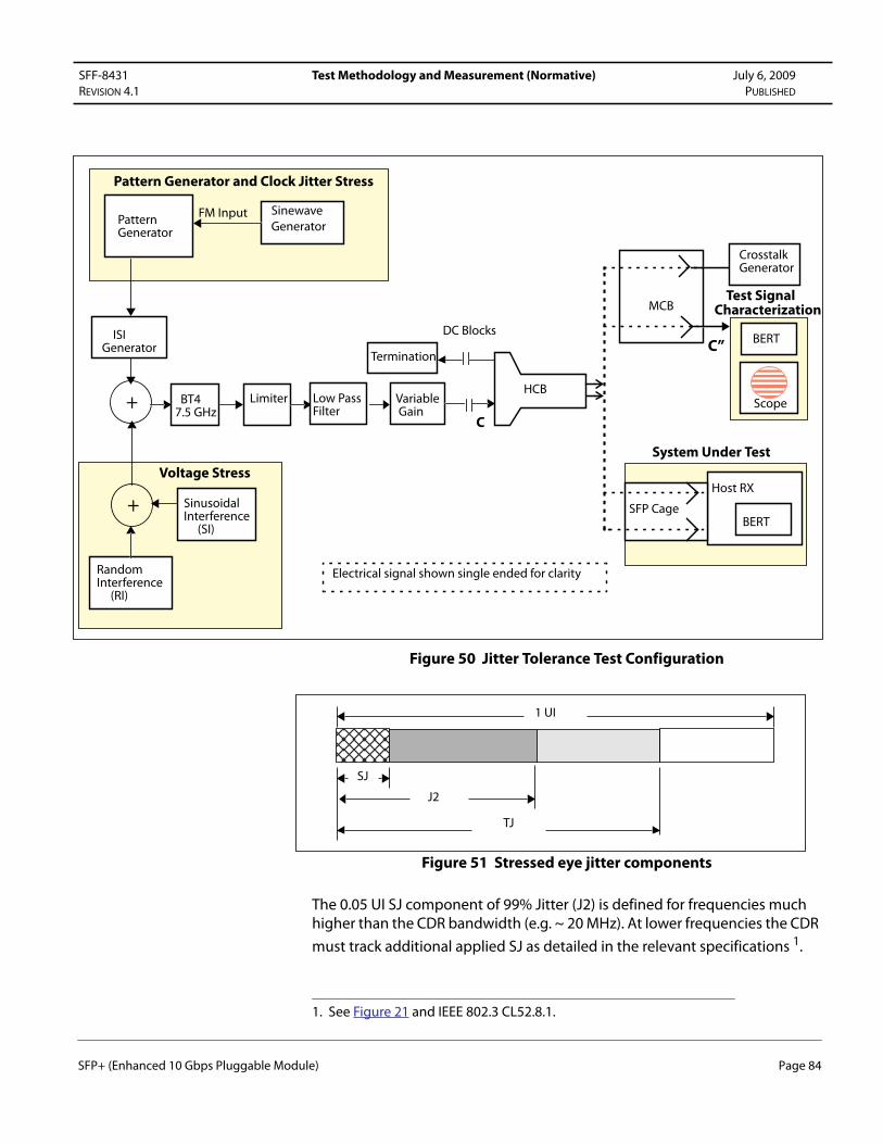
SFF-8431 Test Methodology and Measurement (Normative) July 6, 2009
REVISION 4.1 PUBLISHED
Figure 50 Jitter Tolerance Test Configuration
Figure 51 Stressed eye jitter components
The 0.05 UI SJ component of 99% Jitter (J2) is defined for frequencies much higher than the CDR bandwidth (e.g. ~ 20 MHz). At lower frequencies the CDR
must track additional applied SJ as detailed in the relevant specifications 1.
ISI
Pattern
Voltage Stress
Sinewave
Generator
Generator
+
SinusoidalInterference (SI)
Random
(RI)
Pattern Generator and Clock Jitter Stress
Limiter
Test SignalCharacterization
System Under Test
Host RX
BERT
Interference
+
BT4 7.5 GHz
Variable Gain
C”
Generator
FM Input
Low Pass Filter
DC Blocks
C
MCB
HCB
Crosstalk Generator
Termination
BERT
Scope
SFP Cage
Electrical signal shown single ended for clarity
1 UI
SJ
J2
TJ
1. See Figure 21 and IEEE 802.3 CL52.8.1.
SFP+ (Enhanced 10 Gbps Pluggable Module) Page 84
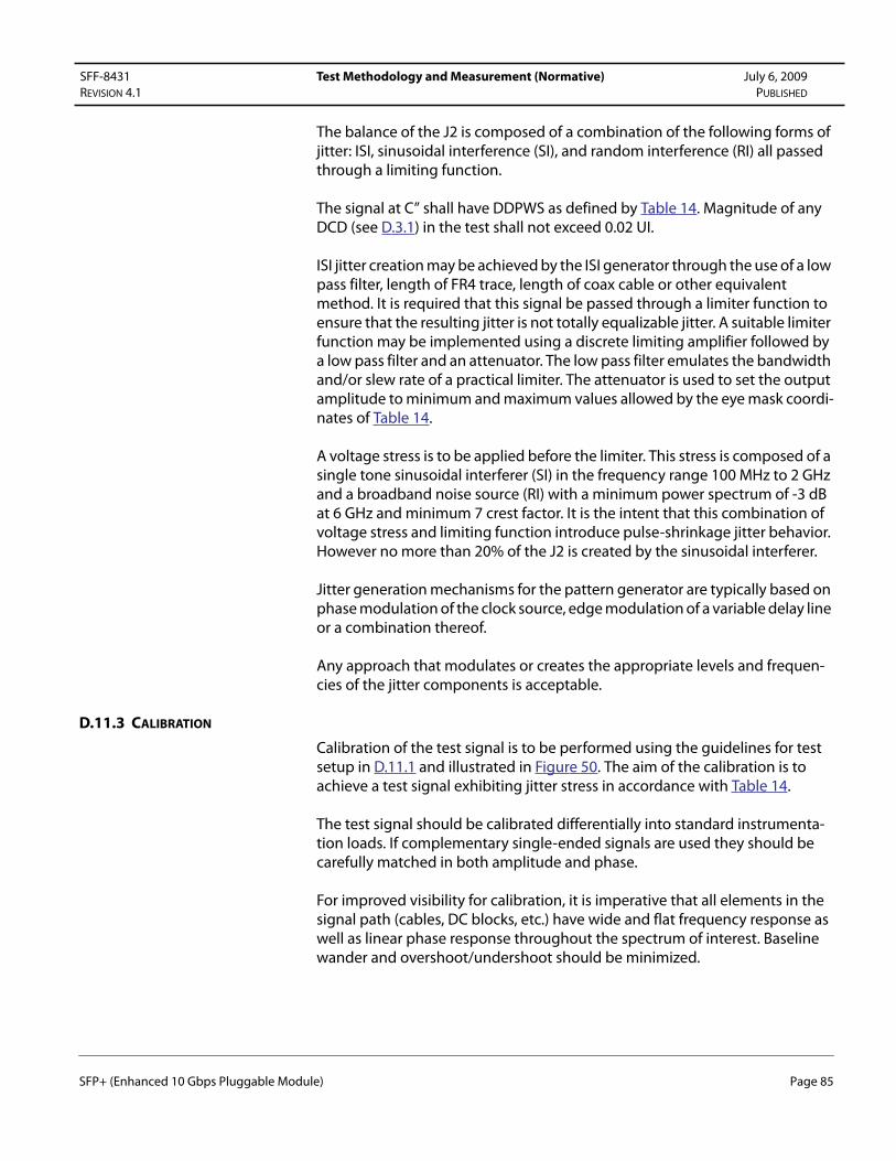
SFF-8431 Test Methodology and Measurement (Normative) July 6, 2009
REVISION 4.1 PUBLISHED
The balance of the J2 is composed of a combination of the following forms of jitter: ISI, sinusoidal interference (SI), and random interference (RI) all passed through a limiting function.
The signal at C” shall have DDPWS as defined by Table 14. Magnitude of any DCD (see D.3.1) in the test shall not exceed 0.02 UI.
ISI jitter creation may be achieved by the ISI generator through the use of a low pass filter, length of FR4 trace, length of coax cable or other equivalent method. It is required that this signal be passed through a limiter function to ensure that the resulting jitter is not totally equalizable jitter. A suitable limiter function may be implemented using a discrete limiting amplifier followed by a low pass filter and an attenuator. The low pass filter emulates the bandwidth and/or slew rate of a practical limiter. The attenuator is used to set the output amplitude to minimum and maximum values allowed by the eye mask coordi-nates of Table 14.
A voltage stress is to be applied before the limiter. This stress is composed of a single tone sinusoidal interferer (SI) in the frequency range 100 MHz to 2 GHz and a broadband noise source (RI) with a minimum power spectrum of -3 dB at 6 GHz and minimum 7 crest factor. It is the intent that this combination of voltage stress and limiting function introduce pulse-shrinkage jitter behavior. However no more than 20% of the J2 is created by the sinusoidal interferer.
Jitter generation mechanisms for the pattern generator are typically based on phase modulation of the clock source, edge modulation of a variable delay line or a combination thereof.
Any approach that modulates or creates the appropriate levels and frequen-cies of the jitter components is acceptable.
D.11.3 CALIBRATION
Calibration of the test signal is to be performed using the guidelines for test setup in D.11.1 and illustrated in Figure 50. The aim of the calibration is to achieve a test signal exhibiting jitter stress in accordance with Table 14.
The test signal should be calibrated differentially into standard instrumenta-tion loads. If complementary single-ended signals are used they should be carefully matched in both amplitude and phase.
For improved visibility for calibration, it is imperative that all elements in the signal path (cables, DC blocks, etc.) have wide and flat frequency response as well as linear phase response throughout the spectrum of interest. Baseline wander and overshoot/undershoot should be minimized.
SFP+ (Enhanced 10 Gbps Pluggable Module) Page 85

SFF-8431 Test Methodology and Measurement (Normative) July 6, 2009
REVISION 4.1 PUBLISHED
An AC coupling 3 dB corner frequency of 20 kHz is expected to be adequate to eliminate baseline wander effects, however high frequency performance is critical and must not be sacrificed by the AC coupling.
Jitter requirements are defined for a probability level of 1x10-12. To calibrate the jitter, methods given in CEI 2.C Annex and MJSQ Chap 8 are recommended. Given random jitter and the nature of the long test patterns, low probability jitter events will likely be present. It is recommended for jitter calibration that a technique that can accurately measure low probability events should be used to avoid overly stressful test conditions.
It is recommended that the actual compliance test pattern be used during cal-ibration. For jitter stress calibration it is permissible, however, to use any appro-priate test pattern which still results in the creation of a compliance test pattern with the appropriate jitter stress.
D.11.4 CALIBRATION PROCEDURE
The vertical eye opening and peak level should be set approximately to the levels specified in Table 14.
With an applied calibration test pattern and no additional jitter stress applied; the intrinsic jitter of the test source due to intrinsic noise and finite bandwidth effects should be measured and calibrated. The 99% jitter (J2) shall be <0.15 UI and TJ <0.25 UI.
SJ should be added until the J2 component of jitter increases by 0.05 UI above the measured reference level. This should be high frequency SJ well above the CDR bandwidth. The SJ frequency should be asynchronous to the character-istic frequency of the signal.
Next, additional high probability jitter as specified in D.11.2 should be added by the ISI generator until at least 80% of the J2 has been created. The Sine In-terferer amplitude should then be turned on and adjusted until the required level of J2 is achieved. The frequency of any Sine interferer should be asyn-chronous to the characteristic frequency of the signal.
A compliant test signal exhibits data dependent pulse width shrinkage as specified in Table 14. Data dependent pulse width shrinkage is defined in D.3. This is measured with noise and clock-jitter sources turned off.
Once the required level of J2 has been achieved turn on the crosstalk source that should be set such that at the output of the Host Compliance Board the amplitude and the rise and fall times should be as given in Table 14. The crosstalk pattern should be PRBS31 or valid 64B/66B signal and should be asynchronous with the data. Then the RI (random interference) should be
added until the required value of TJ is achieved at a probability of 1x10-12.
SFP+ (Enhanced 10 Gbps Pluggable Module) Page 86

SFF-8431 Test Methodology and Measurement (Normative) July 6, 2009
REVISION 4.1 PUBLISHED
If necessary the sine interferer should be readjusted to obtain the required level of J2 and if the sine interferer is changed then the random interferer should be readjusted to obtain the required level of TJ. Iterative adjustments of the sine interferer and random interferer should be made until the required values of both J2 and TJ are achieved.
If necessary, the vertical eye opening should be readjusted to required levels.
It should be verified that the vertical eye opening and peak level specification is met.
Care must be taken when characterizing the signal used to make receiver tol-erance measurements. The intrinsic noise and jitter introduced by the calibra-tion measurement equipment (e.g. filters, oscilloscope and BERT) must be accounted for and controlled. If equipment imperfections affect the results materially, corrections such as RSS deconvolution of Gaussian noise and jitter should be used.
D.11.5 TEST PROCEDURE
Testing should be performed differentially through a Host Compliance Board (see C.2).
Using a test signal calibrated conforming to D.11.1 and calibrated as per D.11.4, operate the system with an appropriate compliance test pattern for the relevant application (10G Ethernet, 10GFC, or 10G Ethernet with FEC).
All signals and reference clocks that operate during normal operation shall be active during the test including the other host signal path in the duplex pair. The other signal path shall be asynchronous.
The opposing direction bit stream (than the one being tested) shall be asyn-chronous PRBS31 or valid 64B/66B signal.
The sinusoidal jitter is stepped across frequency and amplitude range ac-
cording to Figure 21 while monitoring the BER. The BER shall remain < 1x10-12.
D.12 LIMITING MODULE RECEIVER COMPLIANCE TESTS
Compliance to the specifications at C’ Table 18 and Table 19 must be met over the range of input optical signals specified by standards supported e.g. IEEE 802.3 Clause 52 and calibration procedure defined in Clause 52.9.9.
This test includes the effects of crosstalk within the module and within the Module Compliance Board. The module transmit path is operational. The transmit path input of the Module Compliance Board is connected to a pattern generator and calibrated through a Host Compliance Board. The amplitude
SFP+ (Enhanced 10 Gbps Pluggable Module) Page 87

SFF-8431 Test Methodology and Measurement (Normative) July 6, 2009
REVISION 4.1 PUBLISHED
and rise/fall times are given in Table 18. Testing for compliance at point C’ is done through a Module Compliance Board.
The pattern for the crosstalk source is PRBS31 or a valid 64B/66B sequence. The crosstalk source is asynchronous to the TP3 test source.
The minimum test conditions (vertical eye closure penalty, VECP[min] and stressed eye jitter, J(min) for stressed receiver sensitivity defined in IEEE 802.3 clause 52 were chosen as sufficient to ensure compliant receivers. Conse-quently, test conditions more severe than the minimum requirements repre-sent an overstress condition for which compensation is appropriate.
Compensation for overly stressful VECP is straightforward; the stressed re-ceiver sensitivity (SRS) maximum can be adjusted one-for-one for any VECP overstress (or a small amount of under-stress).
SRS[compensated, dBm] = SRS[max, dBm] + dVECP[overstress, dBo],
where dVECP[overstress] = VECP[measured, dBo] - VECP[min, dBo].
Compensation for overly stressful jitter is less straightforward since definition permits compositions over a trade-off range of deterministic and random jitter. Further, there is no generally accepted practice for compensating deter-ministic jitter and the only recourse is re-calibrating the test source. Fortu-nately, most cases of overly stressful jitter are expected to be due to excessive random jitter.
Where the jitter composition is known or can be measured, any excess random jitter can be backed out of the measured result, or specifications in Table 19, Total Jitter and Eye Mask X1 coordinate, can be adjusted to accommodate the excess input signal.
D.13 TEST METHOD FOR A HOST RECEIVER WITH A LINEAR MODULE
A compliance setup for a host for use with a linear module receiver is shown in Figure 52. The host input at point C is tested for BER compliance with test sig-nals that represent the worst case waveshape and noise properties expected from the output of a module during compliant operation.
SFP+ (Enhanced 10 Gbps Pluggable Module) Page 88
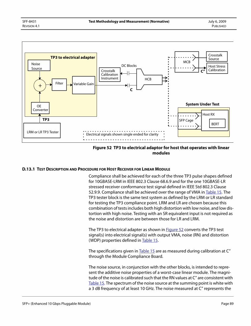
SFF-8431 Test Methodology and Measurement (Normative) July 6, 2009
REVISION 4.1 PUBLISHED
Figure 52 TP3 to electrical adaptor for host that operates with linear modules
D.13.1 TEST DESCRIPTION AND PROCEDURE FOR HOST RECEIVER FOR LINEAR MODULE
Compliance shall be achieved for each of the three TP3 pulse shapes defined for 10GBASE-LRM in IEEE 802.3 Clause 68.6.9 and for the one 10GBASE-LR stressed receiver conformance test signal defined in IEEE Std 802.3 Clause 52.9.9. Compliance shall be achieved over the range of VMA in Table 15. The TP3 tester block is the same test system as defined by the LRM or LR standard for testing the TP3 compliance point. LRM and LR are chosen because this combination of tests includes both high distortion with low noise, and low dis-tortion with high noise. Testing with an SR equivalent input is not required as the noise and distortion are between those for LR and LRM.
The TP3 to electrical adapter as shown in Figure 52 converts the TP3 test signal(s) into electrical signal(s) with output VMA, noise (RN) and distortion (WDP) properties defined in Table 15.
The specifications given in Table 15 are as measured during calibration at C” through the Module Compliance Board.
The noise source, in conjunction with the other blocks, is intended to repre-sent the additive noise properties of a worst-case linear module. The magni-tude of the noise is calibrated such that the RN values at C” are consistent with Table 15. The spectrum of the noise source at the summing point is white with a 3 dB frequency of at least 10 GHz. The noise measured at C” represents the
LRM or LR TP3 Tester
+ Variable GainFilter
Host StressNoise
Source
TP3 to electrical adapter
TP3
C”
CrosstalkSource
OEConverter
CrosstalkCalibrationInstrument
DC Blocks
C
System Under Test
Host RX
BERT
MCB
HCB
SFP Cage
Electrical signals shown single ended for clarity
Calibration
SFP+ (Enhanced 10 Gbps Pluggable Module) Page 89
SFF-8431 Test Methodology and Measurement (Normative) July 6, 2009
REVISION 4.1 PUBLISHED
noise of the module and the optical signal combined. The noise source crest factor should be at least 6.
The filter and gain blocks are intended to represent the deterministic dWDP and gain properties of a worst-case linear module. For the low WDP cases in Table 15, including LR, the filter has a bandwidth of 7.5 GHz. For the high WDP cases in Table 15, the frequency response of the filter is set such that the WDP value specified in Table 15 at C” for the split-symmetrical LRM stressor is achieved. This bandwidth is expected to be approximately 4.5 GHz. In all cases, the overall response of the adapter has a Bessel Thomson response.
The gain block and/or the input optical power level can be used to adjust VMA.
During calibration and host compliance testing, crosstalk source see Figure 52 shall be an asynchronous PRBS31 or 64B/66B signal.
Care must be taken to not induce greater than 0.02 UI of DCD at C”
A balun or other means provides a differential signal.
The test signal output shall be AC coupled. An AC coupling 3 dB corner fre-quency of 20 kHz is expected to be adequate to eliminate baseline wander ef-fects, however high frequency performance is critical and must not be sacrificed by the AC coupling.
The output return loss properties of the test system when measured with Module Compliance Board shall be at least 2 dB better than the specifications of Table 18 up to 8GHz and 1 dB better up to 11GHz.
Any implementation of the measurement configuration may be used, pro-vided that the resulting signal and noise match those defined in Table 15.
Under all specified test conditions, a BER of better than 1x10-12 shall be achieved. The transmitter of the port under test and all other ports operate in normal operation, including termination. The transmitter of the port being tested is terminated through the Host Compliance Board with a DC block and 50 Ω at each Tx SMA connector.
D.13.2 HOST LINEAR TESTER CALIBRATION
The output of the Host Compliance Board is plugged through the Module Compliance Board into laboratory equipment for calibration.
Calibration should be done with all tester elements in place, although some components may be shut down, such as jitter and noise, while other elements are being calibrated - see below. After calibration is completed, all compo-nents are set to their calibrated levels for testing.
SFP+ (Enhanced 10 Gbps Pluggable Module) Page 90

SFF-8431 Test Methodology and Measurement (Normative) July 6, 2009
REVISION 4.1 PUBLISHED
RN of the host test system is adjusted via the magnitude of the adapter’s noise source. Calibration should use the RN measurement methods given in section D.8. RN values are given in Table 15 for each test condition. The crosstalk source must be calibrated to the requirements in Table 13 and running during calibration of RN. After calibration and during host compliance testing, the crosstalk calibration instrument can be removed and replaced with 50 Ohm terminations, although DC blocking must be maintained.
WDP of the host test system is set via the filter in the adapter. If the calibration is off by a small amount, the ISI generator in the TP3 tester can be adjusted to obtain the required values.
Although WDP is a characteristic of an electrical signal in this case, its units are in dBo to better align with WDPo out of a linear optical module, which is also given in dBo.
After calibration, the Host Compliance Board is plugged into the host receiver under test for compliance testing.
D.14 LINEAR MODULE RECEIVER COMPLIANCE TESTS
Linear module receiver compliance tests ensure that noise generation, wave-form filtering and other distortion due to the module are kept within accept-able bounds when tested with the optical input signals as specified in the standards supported by the module, e.g. IEEE 802.3 CL 52 and/or CL 68.
D.14.1 LINEAR MODULE RECEIVER NOISE COMPLIANCE TEST
The module receiver can be tested for noise compliance by measuring how much noise it passes and adds to an input test signal. Figure 53 is a block dia-gram of a test system that defines the module receiver noise test.
Figure 53 Linear Module Receiver Noise Test
TP3Tester
DUT Rx
O/E & BT4 Filter
or
Module Oscilloscope
RNi
RN
ComplianceBoard
Crosstalk
Source
SFP+ (Enhanced 10 Gbps Pluggable Module) Page 91
SFF-8431 Test Methodology and Measurement (Normative) July 6, 2009
REVISION 4.1 PUBLISHED
This test includes the effects of crosstalk within the module and the Module Compliance Board. The transmit path input of the Module Compliance Board is connected to a crosstalk source and calibrated through a Host Compliance Board. The crosstalk amplitude and rise/fall times are set to the values given in Table 18. The pattern for the crosstalk source is PRBS31 or a valid 64B/66B signal. The crosstalk source is asynchronous to the TP3 test source. After cali-bration, the Host Compliance Board is replaced with the module under test. The module transmit path is operational during compliance testing.
The TP3 tester should be set to the OMA/VMA pattern for this test as defined in D.7.
The waveform shaping stress of the TP3 tester is enabled. The sinusoidal jitter and/or sinusoidal interference of the TP3 tester should be disabled or set to very low magnitudes for this test.
RNi of the TP3 tester is set to the level specified by the Table 31.
The TP3 tester is connected into the module under test. The module is plugged into the Module Compliance Board, which in turn is connected to the oscilloscope. The relative noise of the module output signal, RN, is then mea-sured. The relative noise measurement method is described in D.8.
Relative noise of the TP3 test signal RNi is characterized through a reference
O/E converter and 4th-order Bessel Thomson filter and a digital oscilloscope. If the noise of the TP3 test source does not match the target value in Table 31, RN can be corrected using the following equation:
where RNmeasured includes the effect of actual TP3 tester noise at the module
output, RNi is the actual TP3 tester noise, and RNi(target) is the target test noise
given in Table 31 for the test conditions.The resulting noise result is to be com-pared against the compliance limit specified in Table 20. Compliance must be met over the range of optical power specified by the standards supported by the module.
RN RNmeasured( )2 1.24 RNi t etarg( ) RNi RNi t etarg( )–( )××–=
SFP+ (Enhanced 10 Gbps Pluggable Module) Page 92

SFF-8431 Test Methodology and Measurement (Normative) July 6, 2009
REVISION 4.1 PUBLISHED
.
For LRM, RNi should be within 1 dBo of the appropriate value given in Table 31.
For LR and SR, RNi should be no more than 1 dBo greater than the appropriate
value in Table 31; any lower value is allowable.
This procedure is described for an oscilloscope as the measuring instrument. However, noise generated by a practical scope can affect the result. The noise due to the scope is calibrated out of the result by subtracting the square of the scope’s noise from the noise of the RN measurement as appropriate, so as to obtain the relative noise associated with the signal under test. For electrical scope noise measurement, the scope inputs are terminated with 50 Ω termi-nation. For optical scope noise measurement, the scope input should have zero light.
D.14.2 LINEAR MODULE RECEIVER DISTORTION PENALTY COMPLIANCE TEST
This section defines dWDP, a measure of waveform filtering and other distor-tion associated with the linear optical receiver. The block diagram dWDP test system that defines linear module receiver distortion test is shown in Figure 54.
Figure 54 Module receiver waveform penalty compliance test
Table 31 Target RNi Values
Application RNi (target)
LRM pre-cursor 0.0219
LRM split-symmetrical 0.0269
LRM post-cursor 0.0213
LR 0.014
SR 0.020
TP3Tester
DUT Rx
O/E & BT4 Filter
orModule ComplianceBoard Oscilloscope
WDPi
WDP0
SFP+ (Enhanced 10 Gbps Pluggable Module) Page 93

SFF-8431 Test Methodology and Measurement (Normative) July 6, 2009
REVISION 4.1 PUBLISHED
• WDPi and WDPo in Figure 54 are measured using the WDP method de-fined in D.9. WDPi of the TP3 test signal is first characterized through an O/E converter and 4th-order Bessel Thomson filter and a digital oscillo-scope. For 10GBASE-LRM, this signal should represent the waveforms de-scribed in IEEE Std. 802.3 CL 68.6.9, and for 10GBASE-LR, this signal represents the waveform described in IEEE Std. 802.3 CL 52.9.9.
• The TP3 tester is removed from the O/E converter and connected into the module under test. The module in turn is plugged into a Module Compli-ance Board which in turn is connected to the oscilloscope. WDPo of the module output signal is then measured.
Although WDPo is based upon measurements of an electrical signal, its units for a linear optical module output are in dBo to allow a direct comparison with the optical input signal in the equation for dWDP below.
The distortion contributed by the module is determined by the following equation:
dWDP is to be compared against the compliance limit specified in Table 20. Each dWDP must comply for each specified TP3 condition. The TP3 tester is the same test system as defined by the relevant standard for testing the TP3 com-pliance point.
D.14.3 LINEAR MODULE RECEIVER OUTPUT DIFFERENTIAL PEAK-PEAK VOLTAGE
A compliant TP3 stress receiver tester for the relevant application (SR, LR, or LRM) is connected to the module receiver input. The OMA test pattern for the application should be used, and all stress impairments such as sine jitter, sine interference, ISI, and noise should be turned off. The rise/fall time should be 47 ps 20-80%. When observed through a 7.5 GHz reference O/E converter, the input waveform should have no overshoot or ripple.
The output of the module is measured with a Module Compliance Board con-nected into an oscilloscope. The measurement bandwidth is 12 GHz. A wider measurement bandwidth is expected to have only a minor effect on the result. If the measurement bandwidth affects the results, it can be corrected for by post processing. Averaging is used to eliminate noise from the measurement. The peak to peak swing of the differential signal is measured and compared against the limit in Table 20.
dWDP WDPo WDPi–=
SFP+ (Enhanced 10 Gbps Pluggable Module) Page 94

SFF-8431 Test Methodology and Measurement (Normative) July 6, 2009
REVISION 4.1 PUBLISHED
D.15 AC COMMON MODE VOLTAGE
The SFI transmitter and channel limit but do not eliminate AC common mode voltage generation. SFI receivers, both module and host, must operate fully with the maximum allowed input common mode voltage. Common mode voltage often gets generated due to the crossing points of the driver outputs (P and N) being shifted from 50%, impedance mismatch, mismatch of the PCB traces, or mode conversion.
D.15.1 DEFINITION OF AC COMMON MODE VOLTAGE
The common mode voltage at any time is the average of signal+ and signal- at that time. The RMS AC common mode voltage is calculated by applying the histogram function over one UI to the common mode signal. As AC common mode generation is very sensitive to the cable or scope delay mismatch, it is recommended to delay match the scope inputs for any measurements.
D.15.2 AC COMMON MODE GENERATION TEST
The test pattern for AC common mode generation is either pattern 1 (BnBi) or pattern 3 (PRBS31) as defined in IEEE CL 52.9.1.1. It is expected that any 64B/66B scrambled signal should give a similar result.
D.15.3 AC COMMON MODE TOLERANCE TEST
The test pattern for AC common mode tolerance is either pattern 1 (BnBi) or pattern 3 (PRBS31) as defined in IEEE CL 52.9.1.1. It is expected that any 64B/66B coded signal should give a similar result.
If the transmitter output does not generate a sufficient amount of AC common mode then the method to generate additional amounts is by adjusting the P and N delay until the right amounts is generated.
D.16 TERMINATION MISMATCH
Termination mismatch is defined as the percent difference between the com-plimentary Zp and Zn resistors as shown in Figure 18. Termination mismatch is
defined as:
Alternatively, the termination mismatch can be measured by applying a low frequency test tone to the differential inputs as shown in Figure 55. The test frequency must be high enough to overcome the high pass effects of the AC
ΔZM 2Z p Zn–
Z p Zn+------------------× 100×=
SFP+ (Enhanced 10 Gbps Pluggable Module) Page 95

SFF-8431 Test Methodology and Measurement (Normative) July 6, 2009
REVISION 4.1 PUBLISHED
coupling capacitor. The measured differential output or input impedance is designated by Zdiff.
Low frequency termination mismatch is then given by:
where Ip and In are the current flowing into the SFI port as shown in Figure 55.
Zs is the effective series impedance between the driver terminations Zp and Zn
and the AC Ground.
Figure 55 AC Termination Mismatch Measurement
D.17 POWER SUPPLY TESTING METHODOLOGY
This section defines power supply noise output as given in 2.8.2 and 2.8.3, and power supply noise tolerance as in 2.8.4.
The reference power supply filter shown in Figure 56 is provided for module testing, including power supply tolerance testing. This filter will meet the noise filtering requirements in most host systems. Other filtering implementations or local regulation may be used to meet the power noise output requirements described in 2.8.2 and 2.8.3.
For each Vcc, the sum of the equivalent series resistances of the 4.7uH in-ductor, the 22uF capacitor and the damping resistor is 0.5 Ω. This resistance is desirable in actual host filters as well as in the reference filter; however, any voltage drop across a filter network on the host is counted against the host VccT and VccR accuracy specification in Table 8.
ΔZM 2I p In–
I p In+---------------×
Zdiff 100+
Zdiff
------------------------ 100⋅ ⋅=
SFI Port
Capacitor
Capacitor
Test Frequency
50 Ω 0.5%
50 Ω 0.5%
Ip
In
Connector
Zp
Zn
Ground
Zs AC Ground
SFP+ (Enhanced 10 Gbps Pluggable Module) Page 96

SFF-8431 Test Methodology and Measurement (Normative) July 6, 2009
REVISION 4.1 PUBLISHED
Figure 56 Module Compliance Board Power Supply FiltersD.17.1 HOST POWER SUPPLY NOISE OUTPUT
The noise output of a Vcc supply of a host is defined with a resistive load that draws the maximum rated power (1 W or 1.5 W) connected between one Vcc contact and Vee, in place of the SFP+ module. When the noise on VccT is being measured, VccR is left open circuit, and vice versa. 8 Ω is used for a host ca-pable of supporting Power Level II, and 12 Ω otherwise. The AC voltage spec-trum is measured at the module side of the SFP+ connector. The noise power spectrum is divided by the truncated response of the reference filter and then integrated from 10 Hz to 10 MHz and converted to a voltage. This function is illustrated in the equation below and Figure 57. The specification limit is given in 2.8.2. The test is performed with all other portions of the host board/system active. Hosts with multiple SFP+ modules shall test ports one at a time, with ac-tive SFP+ in all the remaining ports.
The reference filter response H(f) shown in Figure 57 and the coefficients a, b, c, d, and e for the 5 frequency bands are defined in Table 32.
Module Compliance Board
Host +3.3V
Point X
SFP+
Module
SFP+ Connector
VccT
VccR
0.1 uF
4.7 uH
4.7 uH
0.1 uF
0.1 uF
22 uF
0.1 uF22 uF
Vee
0.5 Ω
0.1 Ω
0.5 Ω
H f( ) a log 10 f( )( )4× b log 10 f( )( )× 3c log 10 f( )( )× 2
d log 10 f( )( )× e+ + + +=
SFP+ (Enhanced 10 Gbps Pluggable Module) Page 97

SFF-8431 Test Methodology and Measurement (Normative) July 6, 2009
REVISION 4.1 PUBLISHED
Figure 57 Reference filter response
NOTES - As a lightly loaded power supply might generate more noise than a fully loaded supply, the host implementer may wish to assess the host power supply noise output at less than maximum current draw also. Because a small measured noise signal at high frequencies is multiplied up to give the inferred noise at virtual point X, care should be taken over the noise floor of the spec-
Table 32 Truncated Filter Response Coefficients
Frequency (f) a b c d e
10 Hz ≤ f < 100 Hz 0 0 0 0 -0.1
100 Hz ≤ f < 10 kHz 0.3784 -3.6045 12.694 -19.556 11.002
10 kHz ≤ f < 150 kHz -22.67038 430.392 -3053.779 9574.26 -11175.98
150 kHz ≤ f ≤ 5.243 MHz 3.692166 91.467 838.80 -3400.38 5139.285
5.243 MHz ≤ f ≤ 10 MHz 0 0 0 0 -60
SFP+ (Enhanced 10 Gbps Pluggable Module) Page 98

SFF-8431 Test Methodology and Measurement (Normative) July 6, 2009
REVISION 4.1 PUBLISHED
trum analyzer. Other measurement methods could be used, e.g. a measure-ment at a point inside the host, with appropriate consideration to any difference between the reference filter and a host’s actual filter.
D.17.2 SFP+ MODULE POWER SUPPLY NOISE OUTPUT
The module noise voltage output is defined in the frequency band 10 Hz to 10 MHz at point X in Figure 56.
The module must pass module power supply noise output test in all operating modes. This test ensures the module will not couple excessive noise from in-side the module back onto the host board. A power meter technique, or a spectrum analyzer technique with integration of the spectrum, may be used. The maximum allowed noise amplitude is given in 2.8.3.
D.17.3 MODULE POWER SUPPLY TOLERANCE TESTING
In this test, a swept sinusoidal tone is applied at point X of Figure 58 with the tolerance signal amplitude and frequency range given in 2.8.4. The AC toler-ance signal is created by a circuit such as a low impedance buffer amplifier be-tween the power supply and point X. The impedance of the PSU and sine wave generator is less than 0.5 Ω. The amplitude of the sine wave is calibrated at each frequency at point X with the module replaced with a 12 Ω load between Vcc and Vee.
NOTES -- It may be desirable to remove the 0.1 uF capacitors on the host side of the reference filters for this test, to reduce the power needed by the sine wave generator. The calibration of the sine wave is not expected to be signifi-cantly different if the module were in place rather than the test resistor.
Alternatively, the test may be performed separately for VccT and VccR with the other supply filter connected directly to the power supply. It is not necessary to show compliance with both separate and common Vcc modulation.
This test applies at minimum and maximum DC setpoint levels. Note that the DC level is inset to the limits in Table 5 by the peak of the sinusoidal voltage at the input to the module (which is frequency dependent).
The source frequency is varied over the range specified by 2.8.4 to determine if any frequency causes a parameter to fall out of the specification limit. In all cases, the parameters measured shall pass the optical standards with the tone present over all frequencies specified. Parameters of interest for the transmit may include UJ, Qsq and TDP see [IEEE 802.3]. For the receive side, they include
stressed sensitivity, overload, RN and Rx_LOS function.
SFP+ (Enhanced 10 Gbps Pluggable Module) Page 99

SFF-8431 Test Methodology and Measurement (Normative) July 6, 2009
REVISION 4.1 PUBLISHED
Figure 58 Power Supply Noise Tolerance Test Setup
The AC voltage at node X is defined with reference to Vee. The DC voltage specification including ripple, droop and noise below 100 kHz is met at both VccT and VccR (at the SFP+ connector).
PSU and sine
SFP+
Module
SFP+ ConnectorPoint X
VccT
VccR
wave generator
0.1 uF
4.7uH
4.7uH
0.1 uF
0.1 uF
22 uF
0.1 uF22 uF
Vee
(Equivalentcircuit)
Source Resistance
0.5 Ω
0.5 Ω
SFP+ (Enhanced 10 Gbps Pluggable Module) Page 100

SFF-8431 SFP+ Direct Attach Cable Specifications “10GSFP+Cu” (Optional) July 6, 2009
REVISION 4.1 PUBLISHED
APPENDIX E SFP+ DIRECT ATTACH CABLE SPECIFICATIONS “10GSFP+CU” (OPTIONAL)
A passive copper cable compliant to this appendix is identified using the 2-wire management defined in chapter 4 and memory map of SFF-8472.
This appendix describes additional requirements or exceptions to the linear host specification of Chapter 3 to implement passive direct attach SFP+ cable assemblies.
The compliance points for SFP+ Direct Attach Cable (10GSFP+Cu) are the same as host compliance test points 3.3.1 and the module compliance test points in 3.3.2.
All SFI test equipment must have 50 Ohms single ended impedance on all test ports.
Each Tx_Disable contacts of 10GSFP+Cu passive cable assemblies shall be pulled to VccT with a 4.7 kΩ to 10 kΩ in the module. The Rx_LOS contacts in the module shall be pulled low in the module for 10GSFP+Cu passive cable as-semblies. Direct connection of Rx_LOS to VeeR is allowed.
Active cable assemblies must operate with existing linear or limiting specifica-tions of Chapter 3.
This specification does not assume additional transmit pre-emphasis beyond the level required to meet the jitter specifications at point B (see Table 12) and TWDPc specification (see Table 33) at point B. Increasing the transmit pre-em-phasis may increase cable reach, however it may increase transmitter DDJ and is outside the scope of this specification.
Warning: 10GSFP+Cu can only be used on systems with common grounds. Connecting systems with different ground potential with SFP+ direct attach cable results in a short and may cause damage.
E.1 10GSFP+CU DIRECT ATTACH CONSTRUCTION
10GSFP+Cu cable assemblies are effectively constructed out of a pair of SFP+ modules with the OE components replaced with copper cabling as shown in Figure 59. SFP+ Edge card connector contacts are defined in Table 3. The cable assembly shall incorporate DC blocking capacitors with at least 4.3 V rating on the RX side and with high pass pole of between 20 kHz and 100 kHz. The drain wire is connected to VeeT and to VeeR. The cable shield directly connects the module A and B cases.
SFP+ (Enhanced 10 Gbps Pluggable Module) Page 101

SFF-8431 SFP+ Direct Attach Cable Specifications “10GSFP+Cu” (Optional) July 6, 2009
REVISION 4.1 PUBLISHED
Figure 59 10GSFP+Cu Direct Attach Block Diagram
E.2 SFP+ HOST OUTPUT SPECIFICATIONS FOR PASSIVE DIRECT ATTACH CABLES
SFP+ host supporting direct attach cables must meet transmitter output spec-ifications in Table 11 and jitter specifications in Table 12 at reference point B. In addition SFP+ host transmitter must meet the specifications in Table 33.
TWDPc is the host transmitter penalty for copper cable stressor shown in Figure 60 and given in Table 34. Code to calculate TWDPc using this stressor is given in Appendix G.
E.2.1 TRANSMITTER STRESSOR
For TWDPc compliance, a simulated cable response is required. The response is modeled as a set of delta functions with specific amplitudes and delays. The
SFP+ Module Top View of Board
10GSFP+Cu
Cable
End A
DC Blocks
DC Blocks
Ed
ge
Co
nn
ect
or
Ed
ge
Co
nn
ect
or
SFP+ Module Top View of Board
End B
Drain Wire
Cable Shield
TD+
TD-
TD+
TD-
RD+
RD-
RD+
RD-
10GSFP+Cu
Table 33 SFP+ Host Transmitter Output Specifications at B for Cu
Parameters- B Symbol Conditions Min Target Max Units
Voltage Modulation Amplitude (p-p) VMA See D.7 300 mV
Transmitter Qsq Qsq See 1 63.1
Output AC Common Mode Voltage See D.15 12.0 mV (RMS)
Host Output TWDPc TWDPc See 2, 3 10.7 dBe
1. Qsq= 1/RN if the one level and zero level noises are identical and see D.8.
2. Host electrical output measured with LRM 14 taps FFE and 5 taps DFE Equalizer with PRBS9 for copper direct attach stressor, see
Appendix G.3. The stressor for TWDPc is given in Table 34 and is included in the code in Appendix G.
SFP+ (Enhanced 10 Gbps Pluggable Module) Page 102

SFF-8431 SFP+ Direct Attach Cable Specifications “10GSFP+Cu” (Optional) July 6, 2009
REVISION 4.1 PUBLISHED
copper stressor was created from measurements of commonly available direct attach SFP+ cables with the transmitter response de-convolved. The stressor is shown in Figure 60 and the values are listed in Table 34. The sum of all stressor components is normalized to an approximate value of 1.
Figure 60 10GSFP+Cu TWDPc Stressor Impulse Response
0 1 2 3 4 5 6 7 80
0.05
0.1
0.15
0.2
0.25
0.3
0.35
UI
Ampl
itude
Table 34 10GSFP+Cu TWDPc Stressor
Delay (UI) Delay (ns) Amplitude Delay (UI) Delay (ns) Amplitude
0 0 0.0175 4.5 0.43637 0.0270
0.5 0.04849 0.1360 5.0 0.48485 0.0216
1 0.09697 0.2695 5.5 0.53334 0.0202
1.5 0.14546 0.1649 6.0 0.58182 0.0174
2 0.19394 0.0917 6.5 0.63031 0.0146
2.5 0.24243 0.0717 7.0 0.67879 0.0123
3.0 0.29091 0.0498 7.5 0.72728 0.0094
3.5 0.33940 0.0383 8.0 0.77576 0.0066
4.0 0.38788 0.0315
SFP+ (Enhanced 10 Gbps Pluggable Module) Page 103

SFF-8431 SFP+ Direct Attach Cable Specifications “10GSFP+Cu” (Optional) July 6, 2009
REVISION 4.1 PUBLISHED
E.3 SFP+ HOST RECEIVER SUPPORTING 10GSFP+CU INPUT COMPLIANCE TEST SIGNAL CALIBRATED AT C”
A host that is to support the direct attach copper option is to meet the re-
quired 1×10⁻¹² BER when tested with the stressed signal described in Section E.3.1 in addition to the requirements of section 3.5.2 relating to a host receiver supporting linear module.
E.3.1 COPPER HOST RECEIVER SPECIFICATIONS
The SFP+ host receiver stress generator is described by a set of tapped delay lines described in E.3.2, a suitable length of copper cable is expected to gen-erate the stressor described here. The stress generator must meet the target WDPc (Waveform Distortion Penalty for copper) as given in Table 35. The stressor generator shall implement the noise model as captured in Figure 61 using the parameters given in Table 35. The noise model contains two noise sources: Qsq noise which is relative to the transmitter signal level and shaped
by the channel response and No fixed noise (modeling cable NEXT) added post
channel. The added noise sources Qsq and No are white and Gaussian in this
test.
The sensitivity test shall be made with the minimum VMA and the overload test shall be made with the maximum p-p voltage as given in Table 35.
Table 35 10GSFP+ Host receiver input stress Generator at C”
Parameters- C" Symbol Conditions Min Target Max Units
Waveform Distortion Penalty of the ISI Generator WDPc See 1, 2 9.3 dBe
Transmitter Qsq Qsq See 4, 5 63.1
Post channel fixed noise source No See 3 2.14 mV (RMS)
Differential Voltage Modulation Amplitude VMA See 4, D.7 180 mV
Differential Peak-Peak Voltage Overload 700 mV
Input AC Common Mode Voltage See 6, D.15.2 13.5 mV(RMS)
1. Copper stressor as defined in Table 36. WDPc is measured with reference receiver with 14 FFE taps and with 5 DFE taps, see
Appendix G.
2. WDPc for the stress is smaller than the transmitter TWDPc due to the VMA loss in the host stressor.
3. No is the RMS voltage measured over one symbol period at the output of the MCB in a 12 GHz bandwidth. The source for Qsq should be
disabled during this calibration.
4. Square pattern with eight ONEs and eight ZEROs.
5. Qsq= 1/RN if the one level and zero level noises are identical and see D.8. Qsq is calibrated at the output of the MCB in a 12 GHz
bandwidth with the ISI of the channel model in Figure 61 disabled. The source for No should be disabled during this calibration.
6. AC common mode target value is achieved by adjusting relative delay of the P and N signals.
SFP+ (Enhanced 10 Gbps Pluggable Module) Page 104

SFF-8431 SFP+ Direct Attach Cable Specifications “10GSFP+Cu” (Optional) July 6, 2009
REVISION 4.1 PUBLISHED
Figure 61 Block Diagram of Copper Stressor Noise Model
E.3.2 COPPER HOST STRESS GENERATOR 1 UI PULSE RESPONSE
Copper host stressor was created from measurements of commonly available direct attach SFP+ cables. The response of the copper host stress generator 1 UI pulse response is shown in Figure 62 and the pulse response values are listed in Table 36.
A suitable length of copper cable is an acceptable substitute to the stressor of Table 36 provided it has the same WDPc. The RMS fit between the tabulated pulse response in Table 36 and the measured isolated pulse response should be minimized to get the target WDPc values as listed in Table 35.
Figure 62 Stress Generator 1UI Pulse Response with 8x over-sampling
+ +
White Gaussian noise source Qsq
UnstressedTX Signal
Channel Model
Stressed RXCompliance Signal
White Gaussian noise source No
0 2 4 6 8 10 12 140
0.02
0.04
0.06
0.08
0.1
0.12
0.14
UI
Ampl
itude
SFP+ (Enhanced 10 Gbps Pluggable Module) Page 105

SFF-8431 SFP+ Direct Attach Cable Specifications “10GSFP+Cu” (Optional) July 6, 2009
REVISION 4.1 PUBLISHED
Table 36 Stress Generator 1 UI Pulse Response with 8x Over-sampling
Delay (UI) Delay (ns) Amplitude Delay (UI) Delay (ns) Amplitude Delay (UI) Delay (ns) Amplitude
0 0.0000 0.0004 4.625 0.4485 0.0270 9.25 0.8970 0.0093
0.125 0.0121 0.0011 4.75 0.4606 0.0263 9.375 0.9091 0.0092
0.25 0.0242 0.0026 4.875 0.4727 0.0256 9.5 0.9212 0.0089
0.375 0.0364 0.0051 5 0.4848 0.0249 9.625 0.9333 0.0087
0.5 0.0485 0.0094 5.125 0.4970 0.0242 9.75 0.9455 0.0084
0.625 0.0606 0.0158 5.25 0.5091 0.0233 9.875 0.9576 0.0082
0.75 0.0727 0.0246 5.375 0.5212 0.0222 10 0.9697 0.0079
0.875 0.0848 0.0360 5.5 0.5333 0.0212 10.125 0.9818 0.0076
1 0.0970 0.0496 5.625 0.5455 0.0204 10.25 0.9939 0.0073
1.125 0.1091 0.0650 5.75 0.5576 0.0194 10.375 1.0061 0.0070
1.25 0.1212 0.0811 5.875 0.5697 0.0187 10.5 1.0182 0.0068
1.375 0.1333 0.0962 6 0.5818 0.0180 10.6250 1.0303 0.0066
1.5 0.1455 0.1088 6.125 0.5939 0.0174 10.7500 1.0424 0.0065
1.625 0.1576 0.1176 6.25 0.6061 0.0169 10.8750 1.0545 0.0063
1.75 0.1697 0.1218 6.375 0.6182 0.0165 11.0000 1.0667 0.0062
1.875 0.1818 0.1213 6.5 0.6303 0.0161 11.1250 1.0788 0.0061
2 0.1939 0.1169 6.625 0.6424 0.0157 11.2500 1.0909 0.0059
2.125 0.2061 0.1093 6.75 0.6545 0.0155 11.3750 1.1030 0.0058
2.25 0.2182 0.1000 6.875 0.6667 0.0154 11.5000 1.1152 0.0055
2.375 0.2303 0.0899 7 0.6788 0.0153 11.6250 1.1273 0.0052
2.5 0.2424 0.0810 7.125 0.6909 0.0153 11.7500 1.1394 0.0049
2.625 0.2545 0.0732 7.25 0.7030 0.0153 11.8750 1.1515 0.0046
2.75 0.2667 0.0670 7.375 0.7152 0.0153 12.0000 1.1636 0.0044
2.875 0.2788 0.0620 7.5 0.7273 0.0150 12.1250 1.1758 0.0041
3 0.2909 0.0583 7.625 0.7394 0.0146 12.2500 1.1879 0.0039
3.125 0.3030 0.0549 7.75 0.7515 0.0141 12.3750 1.2000 0.0037
3.25 0.3152 0.0519 7.875 0.7636 0.0134 12.5000 1.2121 0.0034
3.375 0.3273 0.0486 8 0.7758 0.0128 12.6250 1.2242 0.0030
3.5 0.3394 0.0455 8.125 0.7879 0.0121 12.7500 1.2364 0.0028
3.625 0.3515 0.0423 8.25 0.8000 0.0115 12.8750 1.2485 0.0026
3.75 0.3636 0.0394 8.375 0.8121 0.0110 13.0000 1.2606 0.0022
3.875 0.3758 0.0367 8.5 0.8242 0.0106 13.1250 1.2727 0.0020
4 0.3879 0.0345 8.625 0.8364 0.0101 13.2500 1.2848 0.0018
4.125 0.4000 0.0324 8.75 0.8485 0.0099 13.3750 1.2970 0.0016
4.25 0.4121 0.0307 8.875 0.8606 0.0097 13.5000 1.3091 0.0014
4.375 0.4242 0.0291 9 0.8727 0.0095 13.6250 1.3212 0.0012
4.5 0.4364 0.0280 9.125 0.8848 0.0094 13.7500 1.3333 0.0009
13.8750 1.3455 0.0008
SFP+ (Enhanced 10 Gbps Pluggable Module) Page 106
SFF-8431 SFP+ Direct Attach Cable Specifications “10GSFP+Cu” (Optional) July 6, 2009
REVISION 4.1 PUBLISHED
E.4 SFP+ PASSIVE DIRECT ATTACH CABLE ASSEMBLY SPECIFICATIONS
Passive direct attach cables are tested with a pair of Module Compliance Boards at compliance point B’ and C’. SFP+ passive cable assemblies need to meet specification in Table 37.
VCR, VMA, Vcm, and dWDP may be derived using frequency based methodol-ogies that yield equivalent results e.g., utilizing frequency dependent crosstalk and insertion loss transfer functions with transmitter behavioral models.
Table 37 10GSFP+Cu Cable Assembly Specifications at B’ and C’
Parameter - C’ (Cable Output) Symbol Conditions Min Target Max Units
Single Ended Input and Output Voltage Tolerance -0.3 4.0 V
Output AC Common Mode Voltage Vcm See 1 13.5 mV (RMS)
Difference Waveform Distortion Penalty dWDPc See 2, 9, E.4.1, E.4.2 and
D.14.2
6.75 dBe
VMA Loss L See 3, 9, D.7, E.4.4 4.4 dBe
VMA Loss to Crosstalk Ratio VCR See 1, D.7, E.4.1, E.4.4 32.5 dB
Differential Output/Input Reflection Coefficient 4 SDDxx
0.01-4.1 GHz See 5 dB
4.1-11.1 GHz See 6 dB
Common Mode Output/Input Reflection
Coefficient 7SCCxx 0.01-2.5 GHz See 10 dB
2.5-11.1 GHz -3 dB
Parameter - B" (Input Test Conditions) Symbol Conditions Min Target Max Units
Input AC Common Mode Voltage Vcm See 1, D.15.2 12 mV (RMS)
Signal Rise and fall time Time Tr/tf See D.6 34 ps
Crosstalk Source Rise/Fall time (20% to 80%) Tr, Tf See D.6 34 ps
Crosstalk Source Amplitude Differential (p-p) 700 mV
WDPi See 8 2.4 dBe
1. When input common mode voltage is 12.0 mV RMS and when input rise and fall times are 34ps and the amplitude is the max amplitude allowed by Table 12.2. Defined with reference receiver with 14 T/2 spaced FFE taps and 5 T spaced DFE taps, see Appendix G.3. VMA loss is the ratio of VMA measured at input and output, respectively.
4. Reference differential impedance is 100 Ω. The dB value listed here are the same as dBe.
5. Reflection Coefficient given by equation SDDxx(dB)= -12 + 2 × SQRT(f), with f in GHz.
6. Reflection Coefficient given by equation SDDxx(dB)= -6.3 + 13 × log10(f/5.5), with f in GHz.
7. Common mode reference impedance is 25 Ω. The dB value listed here are the same as dBe
8. Adjust DDJ and/or DDPWS by adjusting pre-emphasis until the target WDPi is achieved.
9. With input test condition given by parameters B" given in this table.
10. Reflection coefficient given by equation SCCxx(dB) < -7 + 1.6 ×f, with f in GHz.
SFP+ (Enhanced 10 Gbps Pluggable Module) Page 107
SFF-8431 SFP+ Direct Attach Cable Specifications “10GSFP+Cu” (Optional) July 6, 2009
REVISION 4.1 PUBLISHED
E.4.1 SFP+ DIRECT ATTACH CABLE TEST SETUP
Direct attach cable testing methodology is based on the SFP+ test method-ology as defined in section 3.3. The cable is measured through a pair of Module Compliance Boards as shown in Figure 63. This diagram shows the block dia-gram for testing NEXT on cable A end and for measuring WDP on path 1. To measure NEXT on B end and WDP on path 2 the cable end A and B are reversed. The Compliance Signal Generator is described in Figure 49.
Figure 63 10GSFP+ Cable Test Setup
WDPi and WDP0 in Figure 64 use the WDP method defined in D.9. WDPi for
copper is measured by plugging Host Compliance Board into the Module Compliance Board 1 and then meeting the target WDPi as listed in Table 37. WDP0 is measured by plugging one end of the cable in to Module Compliance
Board 1 and the other end in to the Module Compliance Board 2. B” Stress Gen-erator can be the test system described in D.10.
MCB 1
Connector
10GSFP+CuTrace Length
Oscilloscope A
MCB 2
Connector
Trace Length
Oscilloscope B
A End
B End
2x50 ΩTermination
DC Blocks
DC Blocks
Compliance Signal
C’
C’
B’
B’
Generator
Path 1 Path 2
10GSFP+Cu
SFP+ (Enhanced 10 Gbps Pluggable Module) Page 108

SFF-8431 SFP+ Direct Attach Cable Specifications “10GSFP+Cu” (Optional) July 6, 2009
REVISION 4.1 PUBLISHED
Figure 64 10GSFP+Cu Cable NEXT dWDP Test Setup
E.4.2 CABLE DWDP TEST PROCEDURE
The measurement procedure for dWDP is described below:
• The compliance signal generator is set to the PRBS9.
• To improve measurement accuracy, uncorrelated jitter and noise should be reduced.
• Averaging should be used to further reduce instrumentation and measurement noise so their effect on the results are negligible.
• To calibrate WDPi per Table 37, refer to Figure 64. Plug a Host Compli-ance Board into the Module Compliance Board connected to the pat-tern generator. Adjust input rise and fall times to the target value as in Table 37. Adjust DDJ and DDPWS to obtain WDPi given by Table 37. Varying pre-emphasis as described in D.10 is an acceptable method.
• Unplug the Host Compliance Board and connect the cable assembly to the Module Compliance Board as shown in Figure 64. Measure WD Po.
• dWDP = WDPo - WDPi.
E.4.3 CABLE NEXT MEASUREMENT PROCEDURE
Cable NEXT is measured based on the following procedure using the test setup shown in Figure 63:
• The Compliance Signal Generator should be calibrated via a Host Compliance Board inserted into the Module Compliance Board. The output of the Host Compliance Board is point B”.
• The Compliance Signal Generator amplitude and rise and fall times at B” are calibrated to the crosstalk target values as defined in Table 37.
Compliance
or
Host ComplianceBoard
Oscilloscope
WDPi
WDP0
Generator
ModuleCompliance Board 1
Direct Attach
ModuleCompliance
Board 2SFP+ Cable (path 1)End A End B
Signal
A or BVMA0
VMAi
SFP+ (Enhanced 10 Gbps Pluggable Module) Page 109

SFF-8431 SFP+ Direct Attach Cable Specifications “10GSFP+Cu” (Optional) July 6, 2009
REVISION 4.1 PUBLISHED
• The Compliance Signal Generator DDJ and DDPWS at B” should meet or be less than the target specified in Table 17.
• The pattern for the Compliance Signal Generator is PRBS31.
• Module Compliance Board B outputs and inputs are terminated in 50 Ω.
• NEXT is the RMS voltage measured by Oscilloscope A in a bandwidth of 12 GHz. Oscilloscope A should be free running (not triggered).
• The inherent Oscilloscope noise may be corrected by the RSS of Gaus-sian noise from the measured NEXT result.
• The far end Module Compliance Board outputs and input are termi-nated in to 50 Ω.
• This measurement is then repeated for the other cable end.
E.4.4 VMA TO CROSSTALK RATIO (VCR)
Cable VMA loss (L) for cable path 1 can be measured using the test setup shown in Figure 64. VMA loss (L) for cable path 2 is measured by reversing cable end A with B.
Where VMAi is the measured VMA at B” and VMAo is measured at C’.
VMA/2 to crosstalk ratio (VCR) is the ratio of the transmitter minimum VMA at B” Table 33 divided by the cable NEXT which already incorporates reflective
FEXT. The factor 0.3 in the VCR 1 equation accounts for SFP+ finite host return loss.
where
1. VCR equation can be as the following 20*log10(VMAMIN/(2*NEXT*(1+C)))-L.
L dBe( ) 20VMAi
VMAo
---------------⎝ ⎠⎛ ⎞log=
VCR dBe( ) VNR L– K– 20– 10 1 C+( )log=
C 0.3 10
2L
20------–⎝ ⎠
⎛ ⎞
×=
SFP+ (Enhanced 10 Gbps Pluggable Module) Page 110
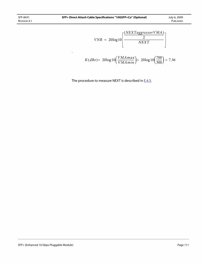
SFF-8431 SFP+ Direct Attach Cable Specifications “10GSFP+Cu” (Optional) July 6, 2009
REVISION 4.1 PUBLISHED
.
The procedure to measure NEXT is described in E.4.3.
VNR 20 10
NEXTaggressorVMA( )2
--------------------------------------------------------
NEXT--------------------------------------------------------log=
K dBe( ) 20 10VMAmax
VMAmin-----------------------⎝ ⎠
⎛ ⎞ 20 10700
300--------⎝ ⎠
⎛ ⎞log 7.36==log=
SFP+ (Enhanced 10 Gbps Pluggable Module) Page 111
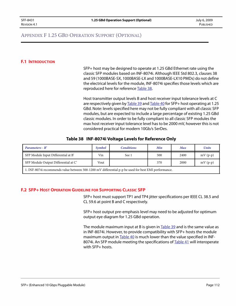
SFF-8431 1.25 GBd Operation Support (Optional) July 6, 2009
REVISION 4.1 PUBLISHED
APPENDIX F 1.25 GBD OPERATION SUPPORT (OPTIONAL)
F.1 INTRODUCTION
SFP+ host may be designed to operate at 1.25 GBd Ethernet rate using the classic SFP modules based on INF-8074i. Although IEEE Std 802.3, clauses 38 and 59 (1000BASE-SX, 1000BASE-LX and 1000BASE-LX10 PMDs) do not define the electrical levels for the module, INF-8074i specifies those levels which are reproduced here for reference Table 38.
Host transmitter output levels B and host receiver input tolerance levels at C are respectively given by Table 39 and Table 40 for SFP+ host operating at 1.25 GBd. Note: levels specified here may not be fully compliant with all classic SFP modules, but are expected to include a large percentage of existing 1.25 GBd classic modules. In order to be fully compliant to all classic SFP modules the max host receiver input tolerance level has to be 2000 mV, however this is not considered practical for modern 10Gb/s SerDes.
F.2 SFP+ HOST OPERATION GUIDELINE FOR SUPPORTING CLASSIC SFP
SFP+ host must support TP1 and TP4 jitter specifications per IEEE CL 38.5 and CL 59.6 at point B and C respectively.
SFP+ host output pre-emphasis level may need to be adjusted for optimum output eye diagram for 1.25 GBd operation.
The module maximum input at B is given in Table 39 and is the same value as in INF-8074i. However, to provide compatibility with SFP+ hosts the module maximum output in Table 40 is much lower than the value specified in INF-8074i. An SFP module meeting the specifications of Table 41 will interoperate with SFP+ hosts.
Table 38 INF-8074i Voltage Levels for Reference Only
Parameters - B’ Symbol Conditions Min Max Units
SFP Module Input Differential at B’ Vin See 1 500 2400 mV (p-p)
SFP Module Output Differential at C’ Vout 370 2000 mV (p-p)
1. INF-8074i recommends value between 500-1200 mV differential p-p be used for best EMI performance.
SFP+ (Enhanced 10 Gbps Pluggable Module) Page 112

SFF-8431 1.25 GBd Operation Support (Optional) July 6, 2009
REVISION 4.1 PUBLISHED
Figure 65 SFP+ Host Transmitter Output Mask for 1.25 GBd Operation
Table 39 SFP+ Host Transmitter Requirements to Support 1.25 GBd Mode
Parameters - B Symbol Conditions Min Units
Host Output VMA Differential Vout 500 mV
Parameters- B Symbol Conditions Value Units
Eye Mask Y1 See D.2 and
Figure 65
150 mV
Eye Mask Y2 500 mV
-Y2
-Y1
0
Y1
Y2
0.0 1.0
Normalized Time (UI)
Vo
ltag
e d
iffe
ren
tial
Table 40 SFP+ Host Receiver Requirements to Support 1.25 GBd Mode
Parameters - C Symbol Conditions Min Units
Host Input VMA Differential Vin 370 mV
Parameters- C Symbol Conditions Value Units
Eye Mask Y1 See D.2 and
Figure 66
125 mV
Eye Mask Y2 600 mV
SFP+ (Enhanced 10 Gbps Pluggable Module) Page 113

SFF-8431 1.25 GBd Operation Support (Optional) July 6, 2009
REVISION 4.1 PUBLISHED
Figure 66 SFP+ Host Receiver Input Mask for 1.25 GBd Operation.
-Y2
-Y1
0
Y1
Y2
0.0 X1 1-X1 1.0
Normalized Time (UI)
Vo
ltag
e d
iffe
ren
tial
Table 41 SFP Module input and output ranges that can be supported by the SFP+ Host
Parameters - Module Symbol Conditions Min Max Units
SFP Module Input at B’ Vin 500 1 2400 1 mV (p-p)
SFP Module Output at C’ Vout 370 1 1200 mV (p-p)
1. Values are identical to the SFP classic INF-8074i specification.
SFP+ (Enhanced 10 Gbps Pluggable Module) Page 114

SFF-8431 Matlab Code for TWDP July 6, 2009
REVISION 4.1 PUBLISHED
APPENDIX G MATLAB CODE FOR TWDP
%%%%%%%%%%%%%%%%% MATLAB (R) Code for xWDP Computation %%%%%%%%%%%%%%%%%
%% SFF-8431 TWDP Code - PAlloc for Cu is now 14.0 dBe.%% Based on original TWDP methodology described in IEEE Std 802.3aq(TM)-2006
%% Reference: N. L. Swenson, P. Voois, T. Lindsay, and S. Zeng, “Standards%% compliance testing of optical transmitters using a software-based equalizing%% reference receiver”, paper NWC3, Optical Fiber Communication Conference and%% Exposition and The National Fiber Optic Engineers Conference on CD-ROM%% (Optical Society of America, Washin[gton, DC), Feb. 2007.
function [xWDP,MeasuredxMA]=SFF8431xWDP(WaveformFile,EqNf,EqNb,SymbolRate,Usage)%% Example calling syntax:%% [xWDP,MeasuredxMA]=SFF8431xWDP('wavefile.txt',14,5,10.3125,'Optical_WDP')
%% The fields in the example given above should be replaced by the actual values%% being used. WaveformFile should be the actual path\filename for each waveform%% tested. The waveform consists of exactly N samples per unit interval T, where%% N is the oversampling rate. The waveform must be circularly shifted to align%% with the data sequence. The file format for the measured waveform is ASCII%% with a single column of chronological numerical samples, in signal level,%% with no headers or footers.%% EqNf is the # of T/2-spaced feedforward equalizer taps; EqNb is the # of%% T-spaced feedback equalizer taps.%% SymbolRate is in gigabaud.%% Options for Usage are 'Optical_WDP', 'Copper_WDP', and 'Copper_TWDP'.%% 'Optical_WDP' is used in support of Chapter 3 for%% measuring WDPi at the output of an optical TP3 tester,%% measuring WDPo at C' of a linear optical module receiver, and%% calibrating WDP at C'' for testing a host that supports linear optical modules.%% 'Copper_WDP' is used in support of Annex E for%% measuring WDPi and calibrating WDP at B'' for testing a copper cable assembly,%% measuring WDPo at C' of a copper cable assembly (C), and%% calibrating WDP at C'' for testing a host that supports copper cable assemblies%% 'Copper_TWDP' is used for measuring TWDP at B of a host that supports copper%% cable assemblies. %% Transmit data file: The transmit data sequence is the 511 bit PRBS9 TWDP test%% patterns defined in Table 686. The file format is ASCII with a single column%% of chronological ones and zeros with no headers or footers.TxDataFile = 'prbs9_950.txt';
%% Program constants %%OverSampleRate = 16; % Oversampling rate, must be evenSymbolPeriod = 1/SymbolRate; % Symbol period is in nsQ0 = 7.03; % BER = 10^(-12)
%% Load input waveform and data sequence, generate filter and other matricesyout0 = load(WaveformFile);XmitData = load(TxDataFile);PtrnLength = length(XmitData);TotLen = PtrnLength*OverSampleRate;Fgrid = [-TotLen/2:TotLen/2-1].'/(PtrnLength*SymbolPeriod);%% Compute response of 7.5 GHz 4th order Butterworth antialiasing filter
SFP+ (Enhanced 10 Gbps Pluggable Module) Page 115

SFF-8431 Matlab Code for TWDP July 6, 2009
REVISION 4.1 PUBLISHED
a = [1 123.1407 7581.811 273453.7 4931335]; % Denominator polynomialb = 4931335; % Numerator for frequency responseExpArg = -j*2*pi*Fgrid;H_r = b./polyval(a,-ExpArg);
%% Get usage parameters for the application[H_chan,Delays,PAlloc,dBscale] = GetParams(Usage,ExpArg);N0 = SymbolPeriod/2 / (Q0 * 10^(PAlloc/dBscale))^2;
%% Set search range for equalizer delay, specified in symbol periods. Lower end%% of range is minimum channel delay. Upper end of range is the sum of the%% lengths of the FFE and channel. Round up and add 5 to account for the%% antialiasing filter.EqDelMin = floor(min(Delays)/SymbolPeriod); EqDelMax = ceil(EqNf/2 + max(Delays)/SymbolPeriod);
ONE=ones(PtrnLength,1);%% Normalize the received xMA (OMA or VMA) to 1. Estimate the xMA of the captured%% waveform by using a linear fit to estimate a pulse response, synthesize a%% square wave, and calculate the xMA of the synthesized square wave per IEEE%% 802.3, clause 52.9.5.ant=4; mem=40; % Anticipation and memory parameters for linear fitX=zeros(ant+mem+1,PtrnLength); % Size data matrix for linear fitY=zeros(OverSampleRate,PtrnLength); % Size observation matrix for linear fitfor ind=1:ant+mem+1 X(ind,:)=circshift(XmitData,ind-ant-1)'; % Wrap appropriately for lin fitendX=[X;ones(1,PtrnLength)]; % The all-ones row is included to compute the biasfor ind=1:OverSampleRate Y(ind,:)=yout0([0:PtrnLength-1]*OverSampleRate+ind)'; % Each column is 1 bitendQmat=Y*X'*(X*X')^(-1); % Coefficient matrix resulting from linear fit. Each %% column (except the last) is one bit period of the pulse response. The last%% column is the bias.SqWvPer=16; % Even number; sets the period of the sq wave used to compute xMASqWv=[zeros(SqWvPer/2,1);ones(SqWvPer/2,1)]; % One period of sq wave (column)X=zeros(ant+mem+1,SqWvPer); % Size data matrix for synthesisfor ind=1:ant+mem+1 X(ind,:)=circshift(SqWv,ind-ant-1)'; % Wrap appropriately for synthesisendX=[X;ones(1,SqWvPer)]; % Include the biasY=Qmat*X;Y=Y(:); % Synthesize the modulated square wave, put into one columnY=AlignY(Y,SqWvPer,OverSampleRate); avgpos=[0.4*SqWvPer/2*OverSampleRate:0.6*SqWvPer/2*OverSampleRate];ZeroLevel=mean(Y(round(avgpos),:)); % Average over middle 20% of "zero" run% Average over middle 20% of "one" run, compute xMAMeasuredxMA=mean(Y(round(SqWvPer/2*OverSampleRate+avgpos),:))-ZeroLevel;%% Subtract zero level and normalize xMAyout0 = (yout0-ZeroLevel)/MeasuredxMA;
%% Compute the noise autocorrelation sequence at the output of the front-end%% antialiasing filter and rate-2/T sampler.Snn = N0/2 * fftshift(abs(H_r).^2) * 1/SymbolPeriod * OverSampleRate;Rnn = real(ifft(Snn));
SFP+ (Enhanced 10 Gbps Pluggable Module) Page 116

SFF-8431 Matlab Code for TWDP July 6, 2009
REVISION 4.1 PUBLISHED
Corr = Rnn(1:OverSampleRate/2:end);C = toeplitz(Corr(1:EqNf));
%% Compute the minimum slicer MSE and corresponding xWDPX = toeplitz(XmitData, [XmitData(1); XmitData(end:-1:end+1-EqNb)]);Xtil = toeplitz(circshift(XmitData,EqDelMin), ... XmitData(mod(-EqDelMin:-1:-(EqDelMax+EqNb),PtrnLength)+1));Rxx = X'*X; % Used in MSE calculation%% Propagate the waveform through channel.yout = real(ifft(fft(yout0) .* fftshift(H_chan)));%% Process signal through front-end antialiasing filter %%%%%%%%%%%%%%%%%%yout = real(ifft(fft(yout) .* fftshift(H_r)));%% Compute MMSE-DFE %%%%%%%%%%%%%%%%%%%%%%%%%%%%%%%%%%% The MMSE-DFE filter coefficients computed below minimize mean-squared error%% at the slicer input. The derivation follows from the fact that the slicer%% input over the period of the data sequence can be expressed as Z = (R+N)*W -%% X*[0 B]', where R and N are Toeplitz matrices constructed from the signal and%% noise components, respectively, at the sampled output of the antialiasing%% filter, W is the feedforward filter, X is a Toeplitz matrix constructed from%% the input data sequence, and B is the feedback filter. The computed W and B%% minimize the mean square error between the input to the slicer and the%% transmitted sequence due to residual ISI and Gaussian noise. Minimize MSE%% over 2/T sampling phase and FFE delay and determine BER.MseOpt = Inf;for jj= [0:OverSampleRate-1]-OverSampleRate/2 % sampling phase %% Sample at rate 2/T with new phase (wrap around as required) yout_2overT = yout(mod([1:OverSampleRate/2:TotLen]+jj-1,TotLen)+1); Rout = toeplitz(yout_2overT, [yout_2overT(1); yout_2overT(end:-1:end-EqNf+2)]); R = Rout(1:2:end, :); RINV = inv([R'*R+PtrnLength*C R'*ONE;ONE'*R PtrnLength]); R=[R ONE]; % Add all-ones column to compute optimal offset Rxr = Xtil'*R; Px_r = Rxr*RINV*Rxr'; %% Minimize MSE over equalizer delay for kk = 1:EqDelMax-EqDelMin+1 SubRange = [kk:kk+EqNb]; SubRange = mod(SubRange-1,PtrnLength)+1; P = Rxx - Px_r(SubRange,SubRange); P00 = P(1,1); P01 = P(1,2:end); P11 = P(2:end,2:end); Mse = P00 - P01*inv(P11)*P01'; if (Mse<MseOpt) MseOpt = Mse; B = -inv(P11)*P01'; % Feedback filter XSel = Xtil(:,SubRange); W = RINV*R'*XSel*[1;B]; % Feedforward filter Z = R*W - XSel*[0;B]; % Input to slicer %% Compute BER using semi-analytic method %%%%%%%%%%%%%%%%%% MseGaussian = W(1:end-1)'*C*W(1:end-1); Ber = mean(0.5*erfc((abs(Z-0.5)/sqrt(MseGaussian))/sqrt(2))); end endend
%% Compute equivalent SNR %%%%%%%%%%%%%%%%%%%%%%%%%%%%%%%%% This function computes the inverse of the Gaussian error probability
SFP+ (Enhanced 10 Gbps Pluggable Module) Page 117
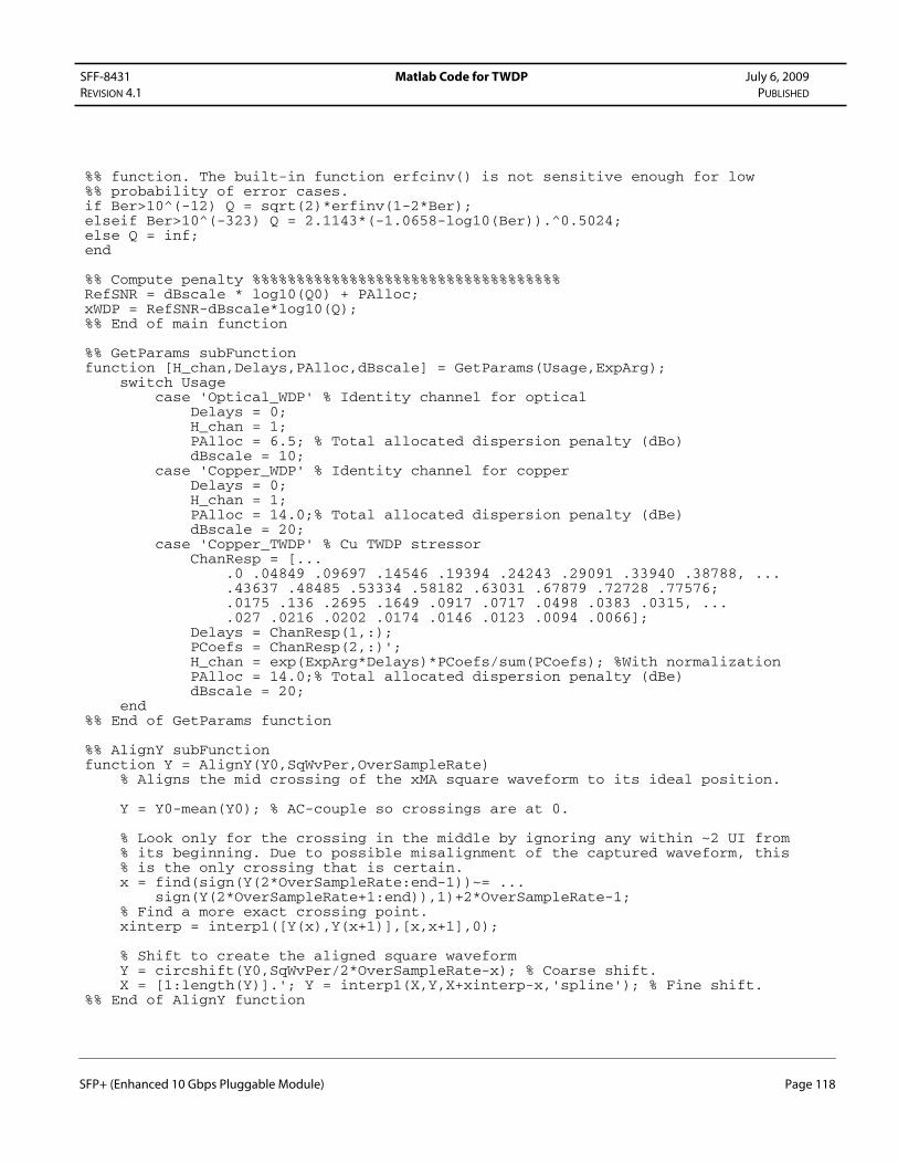
SFF-8431 Matlab Code for TWDP July 6, 2009
REVISION 4.1 PUBLISHED
%% function. The built-in function erfcinv() is not sensitive enough for low%% probability of error cases.if Ber>10^(-12) Q = sqrt(2)*erfinv(1-2*Ber);elseif Ber>10^(-323) Q = 2.1143*(-1.0658-log10(Ber)).^0.5024;else Q = inf;end
%% Compute penalty %%%%%%%%%%%%%%%%%%%%%%%%%%%%%%%%%%%RefSNR = dBscale * log10(Q0) + PAlloc;xWDP = RefSNR-dBscale*log10(Q);%% End of main function
%% GetParams subFunctionfunction [H_chan,Delays,PAlloc,dBscale] = GetParams(Usage,ExpArg); switch Usage case 'Optical_WDP' % Identity channel for optical Delays = 0; H_chan = 1; PAlloc = 6.5; % Total allocated dispersion penalty (dBo) dBscale = 10; case 'Copper_WDP' % Identity channel for copper Delays = 0; H_chan = 1; PAlloc = 14.0;% Total allocated dispersion penalty (dBe) dBscale = 20; case 'Copper_TWDP' % Cu TWDP stressor ChanResp = [... .0 .04849 .09697 .14546 .19394 .24243 .29091 .33940 .38788, ... .43637 .48485 .53334 .58182 .63031 .67879 .72728 .77576; .0175 .136 .2695 .1649 .0917 .0717 .0498 .0383 .0315, ... .027 .0216 .0202 .0174 .0146 .0123 .0094 .0066]; Delays = ChanResp(1,:); PCoefs = ChanResp(2,:)'; H_chan = exp(ExpArg*Delays)*PCoefs/sum(PCoefs); %With normalization PAlloc = 14.0;% Total allocated dispersion penalty (dBe) dBscale = 20; end%% End of GetParams function
%% AlignY subFunctionfunction Y = AlignY(Y0,SqWvPer,OverSampleRate) % Aligns the mid crossing of the xMA square waveform to its ideal position.
Y = Y0-mean(Y0); % AC-couple so crossings are at 0. % Look only for the crossing in the middle by ignoring any within ~2 UI from % its beginning. Due to possible misalignment of the captured waveform, this % is the only crossing that is certain. x = find(sign(Y(2*OverSampleRate:end-1))~= ... sign(Y(2*OverSampleRate+1:end)),1)+2*OverSampleRate-1; % Find a more exact crossing point. xinterp = interp1([Y(x),Y(x+1)],[x,x+1],0); % Shift to create the aligned square waveform Y = circshift(Y0,SqWvPer/2*OverSampleRate-x); % Coarse shift. X = [1:length(Y)].'; Y = interp1(X,Y,X+xinterp-x,'spline'); % Fine shift.%% End of AlignY function
SFP+ (Enhanced 10 Gbps Pluggable Module) Page 118
Top Related