


Languages
Pages
Legal

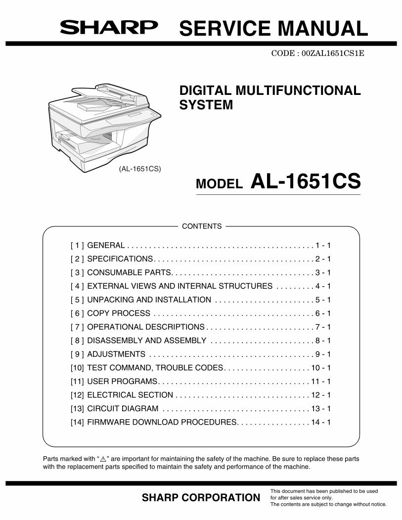
CONTENTS
Parts marked with “ ” are important for maintaining the safety of the machine. Be sure to replace these partswith the replacement parts specified to maintain the safety and performance of the machine.
SHARP CORPORATIONThis document has been published to be usedfor after sales service only.
SERVICE MANUALCODE : 00ZAL1651CS1E
DIGITAL MULTIFUNCTIONAL SYSTEM
MODEL AL-1651CS(AL-1651CS)
[ 1 ] GENERAL . . . . . . . . . . . . . . . . . . . . . . . . . . . . . . . . . . . . . . . . . . . 1 - 1
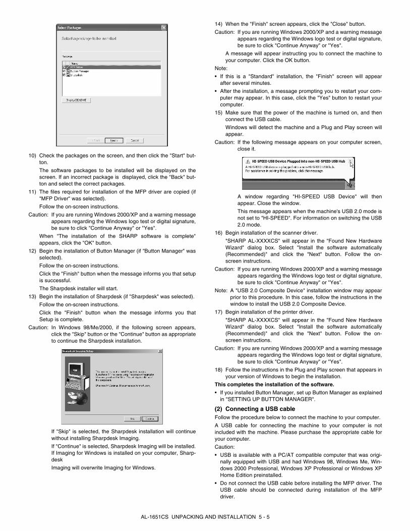
[ 2 ] SPECIFICATIONS. . . . . . . . . . . . . . . . . . . . . . . . . . . . . . . . . . . . . 2 - 1
[ 3 ] CONSUMABLE PARTS. . . . . . . . . . . . . . . . . . . . . . . . . . . . . . . . . 3 - 1
[ 4 ] EXTERNAL VIEWS AND INTERNAL STRUCTURES . . . . . . . . . 4 - 1
[ 5 ] UNPACKING AND INSTALLATION . . . . . . . . . . . . . . . . . . . . . . . 5 - 1
[ 6 ] COPY PROCESS . . . . . . . . . . . . . . . . . . . . . . . . . . . . . . . . . . . . . 6 - 1
[ 7 ] OPERATIONAL DESCRIPTIONS . . . . . . . . . . . . . . . . . . . . . . . . . 7 - 1
[ 8 ] DISASSEMBLY AND ASSEMBLY . . . . . . . . . . . . . . . . . . . . . . . . 8 - 1
[ 9 ] ADJUSTMENTS . . . . . . . . . . . . . . . . . . . . . . . . . . . . . . . . . . . . . . 9 - 1
[10] TEST COMMAND, TROUBLE CODES. . . . . . . . . . . . . . . . . . . . 10 - 1
[11] USER PROGRAMS. . . . . . . . . . . . . . . . . . . . . . . . . . . . . . . . . . . 11 - 1
[12] ELECTRICAL SECTION . . . . . . . . . . . . . . . . . . . . . . . . . . . . . . . 12 - 1
[13] CIRCUIT DIAGRAM . . . . . . . . . . . . . . . . . . . . . . . . . . . . . . . . . . 13 - 1
[14] FIRMWARE DOWNLOAD PROCEDURES. . . . . . . . . . . . . . . . . 14 - 1
The contents are subject to change without notice.
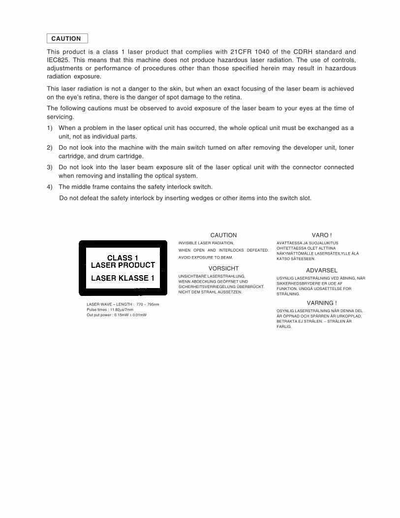
CAUTION
This laser radiation is not a danger to the skin, but when an exact focusing of the laser beam is achievedon the eye’s retina, there is the danger of spot damage to the retina.
The following cautions must be observed to avoid exposure of the laser beam to your eyes at the time ofservicing.
1) When a problem in the laser optical unit has occurred, the whole optical unit must be exchanged as aunit, not as individual parts.
2) Do not look into the machine with the main switch turned on after removing the developer unit, tonercartridge, and drum cartridge.
3) Do not look into the laser beam exposure slit of the laser optical unit with the connector connectedwhen removing and installing the optical system.
4) The middle frame contains the safety interlock switch.
Do not defeat the safety interlock by inserting wedges or other items into the switch slot.
LASER WAVE – LENGTH : 770 ~ 795nmPulse times : 11.82µs/7mmOut put power : 0.15mW ± 0.01mW
CAUTIONINVISIBLE LASER RADIATION,
WHEN OPEN AND INTERLOCKS DEFEATED.
AVOID EXPOSURE TO BEAM.
VORSICHTUNSICHTBARE LASERSTRAHLUNG,WENN ABDECKUNG GEÖFFNET UNDSICHERHEITSVERRIEGELUNG ÜBERBRÜCKT.NICHT DEM STRAHL AUSSETZEN.
VARO !AVATTAESSA JA SUOJALUKITUSOHITETTAESSA OLET ALTTIINANÄKYMÄTTÖMÄLLE LASERSÄTEILYLLE ÄLÄKATSO SÄTEESEEN.
ADVARSELUSYNLIG LASERSTRÅLNING VED ÅBNING, NÅRSIKKERHEDSBRYDERE ER UDE AFFUNKTION. UNDGÅ UDSAETTELSE FORSTRÅLNING.
VARNING !OSYNLIG LASERSTRÅLNING NÄR DENNA DELÄR ÖPPNAD OCH SPÄRREN ÄR URKOPPLAD.BETRAKTA EJ STRÅLEN. – STRÅLEN ÄRFARLIG.
This product is a class 1 laser product that complies with 21CFR 1040 of the CDRH standard and IEC825. This means that this machine does not produce hazardous laser radiation. The use of controls, adjustments or performance of procedures other than those specified herein may result in hazardous radiation exposure.

At the production line, the output powerof the scanner unit is adjusted to 0.57MILLI-WATT PLUS 20 PCTS and ismaintained constant by the operation ofthe Automatic Power Control (APC).Even if the APC circuit fails in operationfor some reason, the maximum outputpower will only be 15 MILLI-WATT 0.1MICRO-SEC. Giving and accessibleemission level of 42 MICRO-WATTwhich is still-less than the limit ofCLASS-1 laser product.
The foregoing is applicable only to the 220Vmodel, 230V model and 240V model.
VAROITUS! LAITTEEN KÄYTTÄMINEN MUULLAKUIN TÄSSÄ KÄYTTÖOHJEESSA MAINITULLATAVALLA SAATTAA ALTISTAA KÄYTTÄJÄNTURVALLISUUSLUOKAN 1 YLITTÄVÄLLENÄKYMÄTTÖMÄLLE LASERSÄTEILYLLE.
VARNING - OM APPARATEN ANVÄNDS PÅ ANNATSÄTT ÄN I DENNA BRUKSANVISNINGSPECIFICERATS, KAN ANVÄNDAREN UTSÄTTASFÖR OSYNLIG LASERSTRÅLNING, SOMÖVERSKRIDER GRÄNSEN FÖR LASERKLASS 1.
CautionThis product contains a low power laserdevice. To ensure continued safety do notremove any cover or attempt to gain accessto the inside of the product. Refer allservicing to qualified personnel.
LUOKAN 1 LASERLAITEKLASS 1 LASER APPARAT

CONTENTS[1] GENERAL
1. Major functions . . . . . . . . . . . . . . . . . . . . . . . . . . . . . . . . . . . . . . . . . . . . . . . 1-12. Note for servicing and handling . . . . . . . . . . . . . . . . . . . . . . . . . . . . . . . . . . 1-1
[2] SPECIFICATIONS1. Basic Specifications . . . . . . . . . . . . . . . . . . . . . . . . . . . . . . . . . . . . . . . . . . . 2-12. Operation specifications . . . . . . . . . . . . . . . . . . . . . . . . . . . . . . . . . . . . . . . . 2-13. Copy performance . . . . . . . . . . . . . . . . . . . . . . . . . . . . . . . . . . . . . . . . . . . . 2-24. SPLC (JBIG GDI) printer . . . . . . . . . . . . . . . . . . . . . . . . . . . . . . . . . . . . . . . 2-35. Scan function . . . . . . . . . . . . . . . . . . . . . . . . . . . . . . . . . . . . . . . . . . . . . . . . 2-36. RSPF . . . . . . . . . . . . . . . . . . . . . . . . . . . . . . . . . . . . . . . . . . . . . . . . . . . . . . 2-3
[3] CONSUMABLE PARTS1. Supply system table . . . . . . . . . . . . . . . . . . . . . . . . . . . . . . . . . . . . . . . . . . . 3-12. Environmental . . . . . . . . . . . . . . . . . . . . . . . . . . . . . . . . . . . . . . . . . . . . . . . 3-13. Production control number(lot No.) identification . . . . . . . . . . . . . . . . . . . . . 3-2
[4] EXTERNAL VIEWS AND INTERNAL STRUCTURES1. Appearance . . . . . . . . . . . . . . . . . . . . . . . . . . . . . . . . . . . . . . . . . . . . . . . . . 4-12. Internal . . . . . . . . . . . . . . . . . . . . . . . . . . . . . . . . . . . . . . . . . . . . . . . . . . . . . 4-13. Operation panel . . . . . . . . . . . . . . . . . . . . . . . . . . . . . . . . . . . . . . . . . . . . . . 4-24. Motors and solenoids . . . . . . . . . . . . . . . . . . . . . . . . . . . . . . . . . . . . . . . . . . 4-35. Sensors and switches . . . . . . . . . . . . . . . . . . . . . . . . . . . . . . . . . . . . . . . . . 4-46. PWB unit . . . . . . . . . . . . . . . . . . . . . . . . . . . . . . . . . . . . . . . . . . . . . . . . . . . 4-57. Cross sectional view. . . . . . . . . . . . . . . . . . . . . . . . . . . . . . . . . . . . . . . . . . . 4-6
[5] UNPACKING AND INSTALLATION1. Copier installation. . . . . . . . . . . . . . . . . . . . . . . . . . . . . . . . . . . . . . . . . . . . . 5-12. Cautions on handling . . . . . . . . . . . . . . . . . . . . . . . . . . . . . . . . . . . . . . . . . . 5-13. Checking packed components and accessories . . . . . . . . . . . . . . . . . . . . . 5-14. Unpacking . . . . . . . . . . . . . . . . . . . . . . . . . . . . . . . . . . . . . . . . . . . . . . . . . . 5-25. Removing protective packing materials . . . . . . . . . . . . . . . . . . . . . . . . . . . . 5-26. Installing the TD cartridge . . . . . . . . . . . . . . . . . . . . . . . . . . . . . . . . . . . . . . 5-27. Loading the paper tray . . . . . . . . . . . . . . . . . . . . . . . . . . . . . . . . . . . . . . . . . 5-38. Power to copier . . . . . . . . . . . . . . . . . . . . . . . . . . . . . . . . . . . . . . . . . . . . . . 5-39. Software for AL-1651CS . . . . . . . . . . . . . . . . . . . . . . . . . . . . . . . . . . . . . . . 5-3
A. Before installation . . . . . . . . . . . . . . . . . . . . . . . . . . . . . . . . . . . . . . . . . 5-4B. Installing the software . . . . . . . . . . . . . . . . . . . . . . . . . . . . . . . . . . . . . . 5-4C. Setting up button manager . . . . . . . . . . . . . . . . . . . . . . . . . . . . . . . . . . 5-8
10. Interface . . . . . . . . . . . . . . . . . . . . . . . . . . . . . . . . . . . . . . . . . . . . . . . . . . . 5-10A. USB . . . . . . . . . . . . . . . . . . . . . . . . . . . . . . . . . . . . . . . . . . . . . . . . . . . 5-10B. RJ45 . . . . . . . . . . . . . . . . . . . . . . . . . . . . . . . . . . . . . . . . . . . . . . . . . . 5-10
11. Moving . . . . . . . . . . . . . . . . . . . . . . . . . . . . . . . . . . . . . . . . . . . . . . . . . . . . 5-10
[6] COPY PROCESS1. Functional diagram. . . . . . . . . . . . . . . . . . . . . . . . . . . . . . . . . . . . . . . . . . . . 6-12. Outline of print process . . . . . . . . . . . . . . . . . . . . . . . . . . . . . . . . . . . . . . . . 6-23. Actual print process . . . . . . . . . . . . . . . . . . . . . . . . . . . . . . . . . . . . . . . . . . . 6-2
[7] OPERATIONAL DESCRIPTIONS1. Outline of operation . . . . . . . . . . . . . . . . . . . . . . . . . . . . . . . . . . . . . . . . . . . 7-12. Scanner section . . . . . . . . . . . . . . . . . . . . . . . . . . . . . . . . . . . . . . . . . . . . . . 7-2
A. Scanner unit. . . . . . . . . . . . . . . . . . . . . . . . . . . . . . . . . . . . . . . . . . . . . . 7-2B. Optical system . . . . . . . . . . . . . . . . . . . . . . . . . . . . . . . . . . . . . . . . . . . . 7-2C. Drive system . . . . . . . . . . . . . . . . . . . . . . . . . . . . . . . . . . . . . . . . . . . . . 7-2
3. Laser unit . . . . . . . . . . . . . . . . . . . . . . . . . . . . . . . . . . . . . . . . . . . . . . . . . . . 7-3A. Basic structure. . . . . . . . . . . . . . . . . . . . . . . . . . . . . . . . . . . . . . . . . . . . 7-3B. Laser beam path . . . . . . . . . . . . . . . . . . . . . . . . . . . . . . . . . . . . . . . . . . 7-3C. Composition. . . . . . . . . . . . . . . . . . . . . . . . . . . . . . . . . . . . . . . . . . . . . . 7-3
4. Fuser section . . . . . . . . . . . . . . . . . . . . . . . . . . . . . . . . . . . . . . . . . . . . . . . . 7-3A. General description . . . . . . . . . . . . . . . . . . . . . . . . . . . . . . . . . . . . . . . . 7-4
5. Paper feed section and paper transport section. . . . . . . . . . . . . . . . . . . . . . 7-4A. Paper transport path and general operations . . . . . . . . . . . . . . . . . . . . 7-4
6. Process unit new drum detection mechanism . . . . . . . . . . . . . . . . . . . . . . . 7-77. RSPF section . . . . . . . . . . . . . . . . . . . . . . . . . . . . . . . . . . . . . . . . . . . . . . . . 7-7
A. Outline . . . . . . . . . . . . . . . . . . . . . . . . . . . . . . . . . . . . . . . . . . . . . . . . . . 7-7B. Document transport path and basic composition. . . . . . . . . . . . . . . . . . 7-7C. Operational descriptions . . . . . . . . . . . . . . . . . . . . . . . . . . . . . . . . . . . . 7-8D. Cases where a document jam is caused. . . . . . . . . . . . . . . . . . . . . . . . 7-8E. RSPF (SPF) open/close detection (book document detection) . . . . . . . 7-8
8. D-D (Duplex to Duplex) mode paper/document transport (Duplex model). . 7-8A. Initial state . . . . . . . . . . . . . . . . . . . . . . . . . . . . . . . . . . . . . . . . . . . . . . . 7-8B. Front copy . . . . . . . . . . . . . . . . . . . . . . . . . . . . . . . . . . . . . . . . . . . . . . . 7-8C. Back copy . . . . . . . . . . . . . . . . . . . . . . . . . . . . . . . . . . . . . . . . . . . . . . . 7-9
9. Shifter . . . . . . . . . . . . . . . . . . . . . . . . . . . . . . . . . . . . . . . . . . . . . . . . . . . . . . 7-9
[8] DISASSEMBLY AND ASSEMBLY1. High voltage section . . . . . . . . . . . . . . . . . . . . . . . . . . . . . . . . . . . . . . . . . . . 8-1
A. List . . . . . . . . . . . . . . . . . . . . . . . . . . . . . . . . . . . . . . . . . . . . . . . . . . . . . 8-1B. Disassembly procedure . . . . . . . . . . . . . . . . . . . . . . . . . . . . . . . . . . . . . 8-1C. Assembly procedure . . . . . . . . . . . . . . . . . . . . . . . . . . . . . . . . . . . . . . . 8-1D. Charger wire cleaning . . . . . . . . . . . . . . . . . . . . . . . . . . . . . . . . . . . . . . 8-1E. Charger wire replacement . . . . . . . . . . . . . . . . . . . . . . . . . . . . . . . . . . . 8-2
2. Operation panel section . . . . . . . . . . . . . . . . . . . . . . . . . . . . . . . . . . . . . . . . 8-2A. List . . . . . . . . . . . . . . . . . . . . . . . . . . . . . . . . . . . . . . . . . . . . . . . . . . . . . 8-2B. Disassembly procedure . . . . . . . . . . . . . . . . . . . . . . . . . . . . . . . . . . . . . 8-2C. Assembly procedure . . . . . . . . . . . . . . . . . . . . . . . . . . . . . . . . . . . . . . . 8-3
3. Optical section . . . . . . . . . . . . . . . . . . . . . . . . . . . . . . . . . . . . . . . . . . . . . . . 8-3A. List . . . . . . . . . . . . . . . . . . . . . . . . . . . . . . . . . . . . . . . . . . . . . . . . . . . . . 8-3B. Disassembly procedure . . . . . . . . . . . . . . . . . . . . . . . . . . . . . . . . . . . . . 8-3C. Assembly procedure . . . . . . . . . . . . . . . . . . . . . . . . . . . . . . . . . . . . . . . 8-4
4. Fusing section . . . . . . . . . . . . . . . . . . . . . . . . . . . . . . . . . . . . . . . . . . . . . . . 8-5A. List . . . . . . . . . . . . . . . . . . . . . . . . . . . . . . . . . . . . . . . . . . . . . . . . . . . . . 8-5B. Disassembly procedure . . . . . . . . . . . . . . . . . . . . . . . . . . . . . . . . . . . . . 8-5C. Assembly procedure . . . . . . . . . . . . . . . . . . . . . . . . . . . . . . . . . . . . . . . 8-7
5. Tray paper feed/transport section . . . . . . . . . . . . . . . . . . . . . . . . . . . . . . . . 8-7A. List . . . . . . . . . . . . . . . . . . . . . . . . . . . . . . . . . . . . . . . . . . . . . . . . . . . . . 8-7B. Disassembly procedure . . . . . . . . . . . . . . . . . . . . . . . . . . . . . . . . . . . . . 8-7
C. Assembly procedure . . . . . . . . . . . . . . . . . . . . . . . . . . . . . . . . . . . . . . .8-126. Manual paper feed section. . . . . . . . . . . . . . . . . . . . . . . . . . . . . . . . . . . . . .8-12
A. List. . . . . . . . . . . . . . . . . . . . . . . . . . . . . . . . . . . . . . . . . . . . . . . . . . . . .8-12B. Disassembly procedure. . . . . . . . . . . . . . . . . . . . . . . . . . . . . . . . . . . . .8-12C. Assembly procedure . . . . . . . . . . . . . . . . . . . . . . . . . . . . . . . . . . . . . . .8-14D. Pressure plate holder attachment . . . . . . . . . . . . . . . . . . . . . . . . . . . . .8-14
7. Rear frame section. . . . . . . . . . . . . . . . . . . . . . . . . . . . . . . . . . . . . . . . . . . .8-14A. List. . . . . . . . . . . . . . . . . . . . . . . . . . . . . . . . . . . . . . . . . . . . . . . . . . . . .8-14B. Disassembly procedure. . . . . . . . . . . . . . . . . . . . . . . . . . . . . . . . . . . . .8-14C. Assembly procedure . . . . . . . . . . . . . . . . . . . . . . . . . . . . . . . . . . . . . . .8-15
8. Power section . . . . . . . . . . . . . . . . . . . . . . . . . . . . . . . . . . . . . . . . . . . . . . .8-15A. List. . . . . . . . . . . . . . . . . . . . . . . . . . . . . . . . . . . . . . . . . . . . . . . . . . . . .8-15B. Disassembly procedure. . . . . . . . . . . . . . . . . . . . . . . . . . . . . . . . . . . . .8-15C. Assembly procedure . . . . . . . . . . . . . . . . . . . . . . . . . . . . . . . . . . . . . . .8-15
9. Duplex motor section (RSPF model only) . . . . . . . . . . . . . . . . . . . . . . . . . .8-15A. Remove the rear cabinet. . . . . . . . . . . . . . . . . . . . . . . . . . . . . . . . . . . .8-15B. Remove the main PWB. . . . . . . . . . . . . . . . . . . . . . . . . . . . . . . . . . . . .8-15C. Remove the Duplex motor. . . . . . . . . . . . . . . . . . . . . . . . . . . . . . . . . . .8-16
10. Reverse roller section (RSPF model only) . . . . . . . . . . . . . . . . . . . . . . . . .8-16A. Remove the reverse unit. . . . . . . . . . . . . . . . . . . . . . . . . . . . . . . . . . . .8-16B. Remove the reverse roller. . . . . . . . . . . . . . . . . . . . . . . . . . . . . . . . . . .8-16
11. RSPF section (RSPF model only) . . . . . . . . . . . . . . . . . . . . . . . . . . . . . . . .8-17A. RSPF. . . . . . . . . . . . . . . . . . . . . . . . . . . . . . . . . . . . . . . . . . . . . . . . . . .8-17B. Intermediate tray . . . . . . . . . . . . . . . . . . . . . . . . . . . . . . . . . . . . . . . . . .8-17C. Upper cover. . . . . . . . . . . . . . . . . . . . . . . . . . . . . . . . . . . . . . . . . . . . . .8-17D. Pickup unit. . . . . . . . . . . . . . . . . . . . . . . . . . . . . . . . . . . . . . . . . . . . . . .8-17E. Upper cover of the pickup unit. . . . . . . . . . . . . . . . . . . . . . . . . . . . . . . .8-18F. Sensor PWB . . . . . . . . . . . . . . . . . . . . . . . . . . . . . . . . . . . . . . . . . . . . .8-18G. Pickup solenoid . . . . . . . . . . . . . . . . . . . . . . . . . . . . . . . . . . . . . . . . . . .8-18H. Clutch . . . . . . . . . . . . . . . . . . . . . . . . . . . . . . . . . . . . . . . . . . . . . . . . . .8-18I. Manual paper feed roller, pickup roller . . . . . . . . . . . . . . . . . . . . . . . . .8-19J. Transport unit removal . . . . . . . . . . . . . . . . . . . . . . . . . . . . . . . . . . . . .8-19K. Belt 1 . . . . . . . . . . . . . . . . . . . . . . . . . . . . . . . . . . . . . . . . . . . . . . . . . . .8-20L. Belt 2 . . . . . . . . . . . . . . . . . . . . . . . . . . . . . . . . . . . . . . . . . . . . . . . . . . .8-20M. SPF motor . . . . . . . . . . . . . . . . . . . . . . . . . . . . . . . . . . . . . . . . . . . . . . .8-20N. Solenoid . . . . . . . . . . . . . . . . . . . . . . . . . . . . . . . . . . . . . . . . . . . . . . . .8-20O. Clutch . . . . . . . . . . . . . . . . . . . . . . . . . . . . . . . . . . . . . . . . . . . . . . . . . .8-20P. Paper supply roller . . . . . . . . . . . . . . . . . . . . . . . . . . . . . . . . . . . . . . . .8-21Q. Paper entry sensor . . . . . . . . . . . . . . . . . . . . . . . . . . . . . . . . . . . . . . . .8-21R. Transport roller 1. . . . . . . . . . . . . . . . . . . . . . . . . . . . . . . . . . . . . . . . . .8-21S. Paper exit roller . . . . . . . . . . . . . . . . . . . . . . . . . . . . . . . . . . . . . . . . . . .8-22T. Solenoid . . . . . . . . . . . . . . . . . . . . . . . . . . . . . . . . . . . . . . . . . . . . . . . .8-23
[9] ADJUSTMENTS1. Optical section . . . . . . . . . . . . . . . . . . . . . . . . . . . . . . . . . . . . . . . . . . . . . . . .9-1
A. Copy magnification ratio adjustment . . . . . . . . . . . . . . . . . . . . . . . . . . . .9-1B. Image position adjustment . . . . . . . . . . . . . . . . . . . . . . . . . . . . . . . . . . .9-2
2. Copy density adjustment . . . . . . . . . . . . . . . . . . . . . . . . . . . . . . . . . . . . . . . .9-3A. Copy density adjustment timing . . . . . . . . . . . . . . . . . . . . . . . . . . . . . . .9-3B. Note for copy density adjustment . . . . . . . . . . . . . . . . . . . . . . . . . . . . . .9-3C. Necessary tool for copy density adjustment . . . . . . . . . . . . . . . . . . . . . .9-4D. Features of copy density adjustment. . . . . . . . . . . . . . . . . . . . . . . . . . . .9-4E. Copy density adjustment procedure . . . . . . . . . . . . . . . . . . . . . . . . . . . .9-4
3. High voltage adjustment . . . . . . . . . . . . . . . . . . . . . . . . . . . . . . . . . . . . . . . .9-5A. Main charger (Grid bias) . . . . . . . . . . . . . . . . . . . . . . . . . . . . . . . . . . . . .9-5B. DV bias check . . . . . . . . . . . . . . . . . . . . . . . . . . . . . . . . . . . . . . . . . . . . .9-5
4. Duplex adjustment . . . . . . . . . . . . . . . . . . . . . . . . . . . . . . . . . . . . . . . . . . . . .9-5A. Adjusting the paper reverse position in memory for duplex copying . . . .9-5B. Adjusting trailing edge void in duplex copy mode . . . . . . . . . . . . . . . . . .9-6
5. SPF (RSPF) scan position automatic adjustment . . . . . . . . . . . . . . . . . . . . .9-76. RSPF (SPF) mode sub scanning direction magnification ratio adjustment . .9-77. Automatic black level correction . . . . . . . . . . . . . . . . . . . . . . . . . . . . . . . . . .9-8
[10] TEST COMMAND, TROUBLE CODES1. Entering the test command mode . . . . . . . . . . . . . . . . . . . . . . . . . . . . . . . .10-12. Key rule . . . . . . . . . . . . . . . . . . . . . . . . . . . . . . . . . . . . . . . . . . . . . . . . . . . .10-13. List of test commands . . . . . . . . . . . . . . . . . . . . . . . . . . . . . . . . . . . . . . . . .10-14. Descriptions of various test commands . . . . . . . . . . . . . . . . . . . . . . . . . . . .10-25. Trouble codes . . . . . . . . . . . . . . . . . . . . . . . . . . . . . . . . . . . . . . . . . . . . . .10-27
A. Trouble codes list . . . . . . . . . . . . . . . . . . . . . . . . . . . . . . . . . . . . . . . .10-27B. Details of trouble codes. . . . . . . . . . . . . . . . . . . . . . . . . . . . . . . . . . . .10-27
[11] USER PROGRAM1. User programs . . . . . . . . . . . . . . . . . . . . . . . . . . . . . . . . . . . . . . . . . . . . . . .11-1
A. Copy mode . . . . . . . . . . . . . . . . . . . . . . . . . . . . . . . . . . . . . . . . . . . . . .11-1B. Print mode . . . . . . . . . . . . . . . . . . . . . . . . . . . . . . . . . . . . . . . . . . . . . . .11-2
2. Selecting a setting for a user program . . . . . . . . . . . . . . . . . . . . . . . . . . . . .11-2
[12] ELECTRICAL SECTION1. Block diagram . . . . . . . . . . . . . . . . . . . . . . . . . . . . . . . . . . . . . . . . . . . . . . .12-1
A. Overall block diagram . . . . . . . . . . . . . . . . . . . . . . . . . . . . . . . . . . . . . .12-12. Circuit descriptions. . . . . . . . . . . . . . . . . . . . . . . . . . . . . . . . . . . . . . . . . . . .12-2
A. Main PWB (MCU) . . . . . . . . . . . . . . . . . . . . . . . . . . . . . . . . . . . . . . . . .12-2B. DC power circuit . . . . . . . . . . . . . . . . . . . . . . . . . . . . . . . . . . . . . . . . .12-11
[13] CIRCUIT DIAGRAM1. MCU PWB . . . . . . . . . . . . . . . . . . . . . . . . . . . . . . . . . . . . . . . . . . . . . . . . . .13-12. OPERATION PWB. . . . . . . . . . . . . . . . . . . . . . . . . . . . . . . . . . . . . . . . . . .13-263. NIC PWB . . . . . . . . . . . . . . . . . . . . . . . . . . . . . . . . . . . . . . . . . . . . . . . . . .13-294. POWER SUPPLY . . . . . . . . . . . . . . . . . . . . . . . . . . . . . . . . . . . . . . . . . . .13-335. ACTUAL WIRING DIAGRAM. . . . . . . . . . . . . . . . . . . . . . . . . . . . . . . . . . .13-35
[14] FIRMWARE DOWNLOAD PROCEDURES1. Download procedures . . . . . . . . . . . . . . . . . . . . . . . . . . . . . . . . . . . . . . . . .14-12. Version acquisition procedures . . . . . . . . . . . . . . . . . . . . . . . . . . . . . . . . . .14-23. EEPROM data acquisition procedure . . . . . . . . . . . . . . . . . . . . . . . . . . . . .14-34. Serial number setting . . . . . . . . . . . . . . . . . . . . . . . . . . . . . . . . . . . . . . . . . .14-45. Installing procedures . . . . . . . . . . . . . . . . . . . . . . . . . . . . . . . . . . . . . . . . . .14-4

AL-1651CS GENERAL 1 - 1
[1] GENERAL
1. Major functionsConfigurations
Descriptions of itemsCPM: Copy speed (Copies Per Minute)
SB/MB: SB = Manual feed single bypass, MB = Manual feed multi bypass
2 tray: Second cassette unit
SPF: Original feed unit
R-SPF: Duplex original feed unit
Color scanner: Color scanner function
GDI printer: GDI printer function with USB
SPLC: SPLC printer function
E-SORT: Electrical sort
Duplex: Auto duplex copy function
Shifter: Job separator function
FAX: FAX function
Sharpdesk: Scanner utilities
IEEE1284: Interface port (parallel)
USB: Interface port (USB)
RJ45: Interface port (Network)
External NIC: Interface port (Network)
Descriptions of table: Standard provision: No function or no option availableOpt: Option
2. Note for servicing and handlingWhen the main unit power is repeatedly turned OFF/ON rapidly (for about 1sec), the IC (OA982) on the MCU PWB may malfunction to cause an error(E1-00 Communication error), which does not boot the machine. In case of this error, the blank display is kept for several tens seconds and then "E1-00" is displayed on the panel display.
<Countermeasure>Turn off the power and keep it for more than 10sec. Then turn on the power.
When the machine is booted.: There is no problem in the MCU PWB.
When the machine is not booted.: The MCU PWB trouble
Item CPM / PPM SB/
MB2
TraySPF R-SPF
Color Scanner (push)
GDI printer
SPLC E-SORT Duplex Shifter FAXSharpdesk
IEEE1284
USB RJ45External
NICModel LT A4
AL-1651CS 16 15 MB
(2.0)
print only
(AL-1651CS)
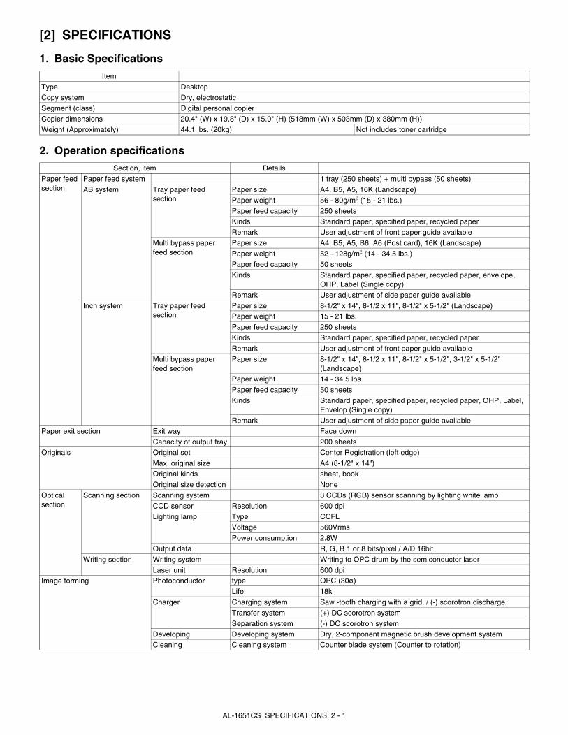
[2] SPECIFICATIONS
1. Basic Specifications
2. Operation specifications
ItemType Desktop
Copy system Dry, electrostatic
Segment (class) Digital personal copier
Copier dimensions 20.4" (W) x 19.8" (D) x 15.0" (H) (518mm (W) x 503mm (D) x 380mm (H))Weight (Approximately) 44.1 lbs. (20kg) Not includes toner cartridge
Section, item Details
Paper feed section
Paper feed system 1 tray (250 sheets) + multi bypass (50 sheets)
AB system Tray paper feed section
Paper size A4, B5, A5, 16K (Landscape)
Paper weight 56 - 80g/m2 (15 - 21 lbs.)
Paper feed capacity 250 sheetsKinds Standard paper, specified paper, recycled paper
Remark User adjustment of front paper guide available
Multi bypass paper feed section
Paper size A4, B5, A5, B6, A6 (Post card), 16K (Landscape)
Paper weight 52 - 128g/m2 (14 - 34.5 lbs.)
Paper feed capacity 50 sheets
Kinds Standard paper, specified paper, recycled paper, envelope, OHP, Label (Single copy)
Remark User adjustment of side paper guide available
Inch system Tray paper feed section
Paper size 8-1/2" x 14", 8-1/2 x 11", 8-1/2" x 5-1/2" (Landscape)Paper weight 15 - 21 lbs.
Paper feed capacity 250 sheets
Kinds Standard paper, specified paper, recycled paper
Remark User adjustment of front paper guide available
Multi bypass paper feed section
Paper size 8-1/2" x 14", 8-1/2 x 11", 8-1/2" x 5-1/2", 3-1/2" x 5-1/2" (Landscape)
Paper weight 14 - 34.5 lbs.
Paper feed capacity 50 sheets
Kinds Standard paper, specified paper, recycled paper, OHP, Label, Envelop (Single copy)
Remark User adjustment of side paper guide available
Paper exit section Exit way Face down
Capacity of output tray 200 sheetsOriginals Original set Center Registration (left edge)
Max. original size A4 (8-1/2" x 14")
Original kinds sheet, book
Original size detection None
Optical section
Scanning section Scanning system 3 CCDs (RGB) sensor scanning by lighting white lamp
CCD sensor Resolution 600 dpiLighting lamp Type CCFL
Voltage 560Vrms
Power consumption 2.8W
Output data R, G, B 1 or 8 bits/pixel / A/D 16bit
Writing section Writing system Writing to OPC drum by the semiconductor laser
Laser unit Resolution 600 dpiImage forming Photoconductor type OPC (30ø)
Life 18k
Charger Charging system Saw -tooth charging with a grid, / (-) scorotron discharge
Transfer system (+) DC scorotron system
Separation system (-) DC scorotron system
Developing Developing system Dry, 2-component magnetic brush development systemCleaning Cleaning system Counter blade system (Counter to rotation)
AL-1651CS SPECIFICATIONS 2 - 1

*1) May fluctuate due to environmental conditions and the input voltage.
3. Copy performance
Fusing section Fusing system Heat roller system
Upper heat roller type Teflon rollerLower heat roller type Silicon rubber roller
Heater lamp type Halogen lamp
Voltage 120V
Power consumption 800W
Electrical section Power source Voltage 120V
Frequency 60HzRated current 8A
Power consumption Max. Less than 1000W
Average (during copying) 350 Wh/H *1)
Average (stand-by) 80Wh/H *1)
Pre-heat mode 25Wh/H *1)
Auto power shut-off mode 8.8Wh/H *1)
Section, item Details
Copy magnification Fixed magnification ratios
4 Reduction + 3 Enlargement (AB system : 25, 50, 70, 86, 100, 141, 200, 400%) (Inch system : 25, 50, 64, 78, 100, 129, 200, 400%)
Zooming magnification ratios
OC: 25 - 400%, RSPF 50 - 200% (376 steps in 1% increments)
Manual steps (text, photo) 5 steps
Copy speed First copy time Tray paper feed 9.6 sec. (Pre-heat mode:25 sec. / Auto power-shut-off mode : 40 sec.) A4 or Letter/100%/Auto Exposure
AB systemA4(Landscape)
Copy speed (CPM) Same size 15
Enlargement 15
Reduction 15AB systemB5(Landscape)
Copy speed (CPM) Same size 15
Enlargement 15
Reduction 15
Inch system8-1/2" x 14"(Landscape)
Copy speed (CPM) Same size 12
Enlargement 12
Reduction 12
Inch system8-1/2" x 11"(Landscape)
Copy speed (CPM) Same size 16Enlargement 16
Reduction 16
Max. continuous copy quantity 99
Void Void area leading edge 1 - 4mm
Trailing edge 4mm or less, 6mm or less (Duplex copying/both image)
Side void area 0.5mm or more (per side)4.5mm or less (total of both sides)
Image loss leading edge Same size: 3.0mm or less (OC) / 4.0mm or less (SPF/R-SPF/Duplex) Enlarge: 1.5mm or less (OC) / 3.0mm or less (SPF/R-SPF/Duplex) Reduction (50%): 6.0mm or less (OC) / 8.0mm or less (SPF/R-SPF/Duplex)
Warm-up time 0 sec.
Power save mode reset time 0 sec.
Paper jam recovery time 0 sec.
Section, item Details
AL-1651CS SPECIFICATIONS 2 - 2

4. SPLC (JBIG GDI) printer
*1: Engine Resolution
*2: Running change
5. Scan function
*1: Running change
6. RSPF
Print speed Max. 15ppm (A4 / with ROPM) / 16ppm (Letter / with ROPM)First print time 9.6 sec. (without data transfer time)
Duplex Yes
ROPM Yes
CPU None
Memory Share the memory with E-SORT function
Interface RJ45 (10 base) / USB 2.0Network Internal NIC
Emulation SPLC (JBIG GDI)
MIB support No
Resolution 600dpi *1
Supported OS Win 95 / 98 / Me / NT 4.0 / 2000 / XP
WHQL support Yes *2Application Status window
Type Flat Bed Color Scanner
Scanning system Document glass/RSPF
Light source 3 CCDs (RGB) sensor scanning by lighting white lamp (2 pcs of CCFL)Resolution Optical: 600 x 1200dpi
Setting range: 50 - 9600dpi (Preview resolution is fixed at 75dpi)
Originals Sheet type / Book typeOutput data R, G, B 1 or 8 bits/pixel / A/D 16bit
Scan range OC / RSPF: 8.5" (297mm) (L) x 14" (431mm) (W)Original position: Platen: Left center / SPF: Right center
Scan speed OC / SPF: Max. 2.88ms/line (Color/Gray scale), Max. 0.96 ms/line (B & W)
Protocol TWAIN / WIA (Only XP) / STI
Support file format RAW / JPEG
Interface USB2.0
Scanner utility Button Manager / Sharpdesk
Scan key/lamp YesDuplex scan No
Supported OS Win 98 / Me / 2000 / XP
Void area No (User settable by PC)
WHQL supported Yes *1
Original capacity 30 sheets (52 to 90g/m2) (14 to 23.9 lbs.)Original size A4 to A5/10" x 14" to 5-1/2" x 8-1/2"
Original replacement speed 12CPM (A4/8-1/2" x 11"Landscape)
Job speed (Tray1,Landscape) Single copy S to S 12CPM
S to D 5.6CPM
D to S 5.5CPM
D to D 5.2CPMMulti copy S to S 16CPM
D to S 16CPM
Original placement Face up
Original weight 52 to 90g/m2(14 - 23.9lbs.)
Mixed feeding No
Original which cannot Thermal papers, originals with punch holes for files, be used folded paper, transparent originals such as OHP films, stapled or clip used originals with cover up liquid used, Originals with tape sealed, originals with high level frictional coefficient such as photos or catalogs.
AL-1651CS SPECIFICATIONS 2 - 3

[3] CONSUMABLE PARTS
1. Supply system table Common to all destinations
2. EnvironmentalThe environmental conditions for assuring the copy quality and the machine operations are as follows:
(1) Normal operating condition
Temperature:20 - 25°CHumidity:65 ± 5%RH
(2) Acceptable operating condition
(3) Optical condition
(4) Supply storage condition
No. Name Content Life Product name Package
1 Develop cartridge (Black) x 1(Except Europe)
Toner/developer cartridge x 1(Toner: Net weight 124g) (Developer: Net weight 190g)
4K(5% document)
AL-110TD 5
2 Drum cartridge Drum cartridge 18K AL-100DR 5
Humidity (RH)
85%
60%
20%
10˚C 30˚C 35˚C
Humidity (RH)
90%
60%
15%
–25˚C 30˚C 40˚C
Humidity (RH)
90%
20%
–5˚C 45˚C
AL-1651CS CONSUMABLE PARTS 3 - 1
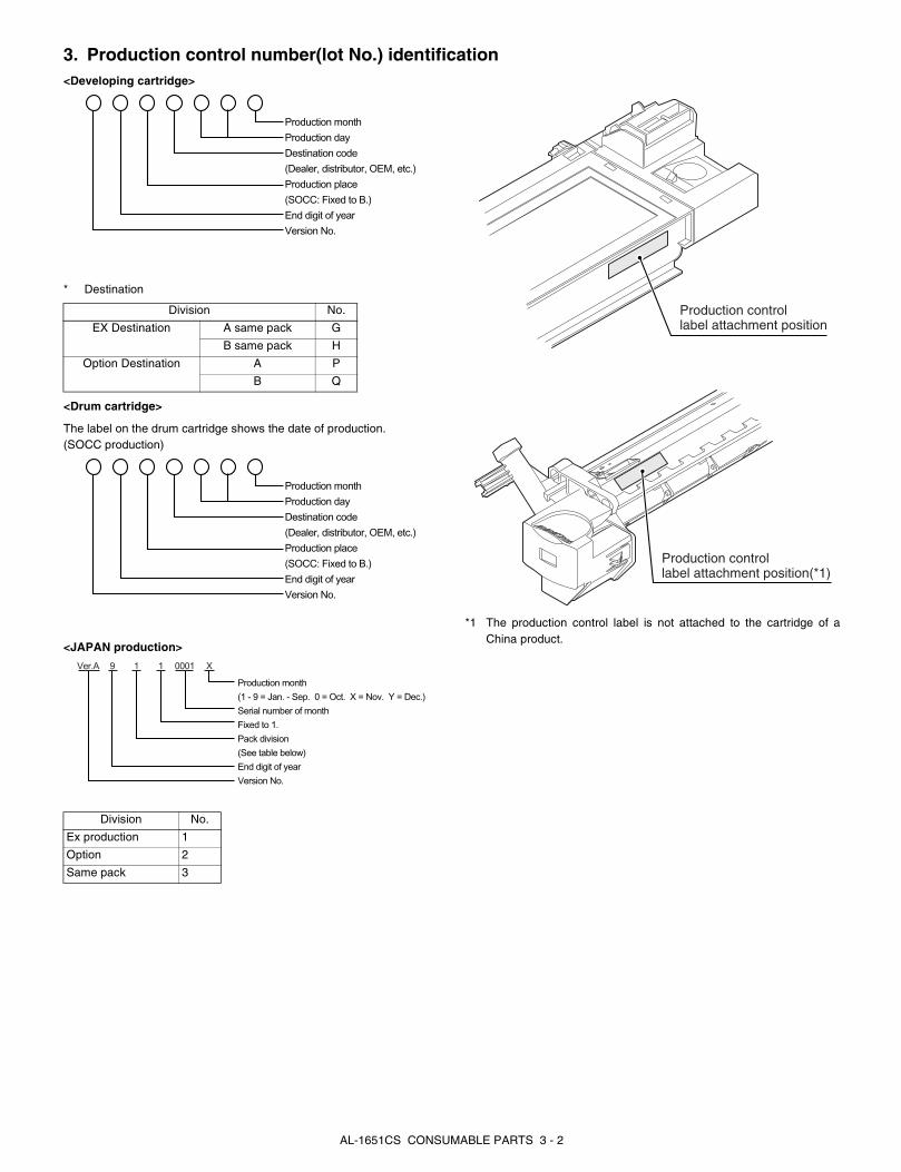
3. Production control number(lot No.) identification<Developing cartridge>
* Destination
<Drum cartridge>
The label on the drum cartridge shows the date of production.(SOCC production)
<JAPAN production>
*1 The production control label is not attached to the cartridge of aChina product.
Division No.
EX Destination A same pack G
B same pack H
Option Destination A P
B Q
Division No.
Ex production 1
Option 2
Same pack 3
Production month
Production day
Destination code
(Dealer, distributor, OEM, etc.)
Production place
(SOCC: Fixed to B.)
End digit of year
Version No.
Production month
Production day
Destination code
(Dealer, distributor, OEM, etc.)
Production place
(SOCC: Fixed to B.)
End digit of year
Version No.
X000119Ver.A 1
Production month
(1 - 9 = Jan. - Sep. 0 = Oct. X = Nov. Y = Dec.)
Serial number of month
Fixed to 1.
Pack division
(See table below)
End digit of year
Version No.
Production controllabel attachment position
Production controllabel attachment position(*1)
AL-1651CS CONSUMABLE PARTS 3 - 2
[4] EXTERNAL VIEWS AND INTERNAL STRUCTURES
1. Appearance
2. Internal
1 Document glass 2 Operation panel 3 Front cover4 Paper tray 5 Side cover 6 Side cover open button
7 Bypass tray paper guides 8 Bypass tray 9 Reversing tray
10 Original guides 11 Document feeder cover 12 Document feeder tray
13 Exit area 14 Paper output tray 15 Paper output tray extension
16 Power switch 17 Handles 18 Power cord
19 USB port 20 LAN port 21 Paper holding arm
1 Side cover 2 Fusing unit release lever 3 Transfer charger
4 Charger cleaner 5 Front cover
2
3
4
1
5
76
8
RSPF9
10
11
1213
Interface
1415
1617
18
19
20
17
21
TD cartridge Drum cartridge
1
5
2
3
4
AL-1651CS EXTERNAL VIEWS AND INTERNAL STRUCTURES 4 - 1
3. Operation panel
1 [MODE SELECT] key / Mode indicatorsPress this key to select the mode. The indicator of the selected mode lights (copy, printer, scanner).
2 DisplayThis shows messages indicating the machine status and any problems that occur, as well as user programs and function setting menus.
3 Numeric keysUse these to enter the number of copies and other numerical settings.The keys can also be used to select items in function setting menus.
4 [CLEAR] key ( )Use this to clear the set number of copies, as well as cancel a job that is in progress. When a setting menu appears, use this key to move back to the previous menu level.
5 Power save indicatorThis lights up when the power save function is activated.
6 RSPF indicatorThis lights up when an original is placed in the RSPF.
7 Error indicatorThis lights steadily or blinks when a paper misfeed or other error occurs.
8 [TRAY SELECT] key ( )Use to select the paper tray that has the desired paper for copying.
9 Tray location indicatorIndicates the selected paper tray. The indicator blinks when the tray is out of paper or is not closed.
10 [MENU] keyPress this key to select the paper size for copying, to configure a user program or to display the total count.
11 [2-SIDED COPY] keyUse to copy both sides of an original.
12 [E-SORT/SP.FUN] keyPress to select the sort function, 2 in 1 copy function, or margin shift function.
13 [ ] key ( ), [ ] key ( ), [ENTER] keyPress the [ ] key ( ) or [ ] key ( ) to select an item in a function setting menu.Press the [ENTER] key to enter a selection.
14 [EXPOSURE] keyUse to switch from auto exposure adjustment to text mode or photo mode.
15 [COPY RATIO] keyPress to select an enlargement or reduction ratio.To select a preset ratio setting, press the [COPY RATIO] key and select the desired preset ratio. To select a ratio that is not preset, press the [COPY RATIO] key, select the preset ratio that is closest to the desired ratio, and then press the [ ] key ( ) or [ ] key ( ) to increase or decrease the ratio in increments of 1%.
16 [START] key ( ) / Ready indicatorThe ready indicator lights up when copying or scanning is possible.To begin copying, press the [START] key ( ).The [START] key ( ) is also pressed to return to normal operation from auto power shut-off mode.
17 [CLEAR ALL] key ( )This returns all functions to the default settings. When pressed in a setting menu, this returns the settings and display to the initial state.
18 Shows the current copy ratio.
19 Shows the selected paper size. 20 Shows the number of copies that has been entered with the numeric keys.
21 A checkmark " " appears when the exposure has been changed, or when two-sided copying, sort, 2 IN 1, or margin shift is selected.
READY TO COPY. 100% 8.5x11 0
Display
AL-1651CS
6 7 8 9 10 11 12 13 14 15 16 17
18 19 20 21
1 2 3 4 5
AL-1651CS EXTERNAL VIEWS AND INTERNAL STRUCTURES 4 - 2

4. Motors and solenoids
No. Part name Control signal Function / Operation
1 Main motor MM Drives the copier.
2 Scanner motor MRMT Drives the optical mirror base (scanner unit).
3 Toner motor TM Supplies toner.4 Cooling fan motor VFM Cools the optical section.
5 Resist roller solenoid RRS Resist roller rotation control solenoid
6 Paper feed solenoid CPFS1 Cassette Paper feed solenoid 1
7 Multi paper feed solenoid MPFS Multi manual pages feed solenoid
8 SPF motor SPFM Drives the single pass feeder
9 Duplex motor DMT Devices the duplex paper transport section10 Original feed solenoid SPUS Original pick up solenoid
11 SPF paper feed solenoid SPFS Original feed solenoid
12 SPF gate solenoid SGS Controls the document reverse gate.
13 Shifter motor SFTM Drives the shifter.
1
4
8
11
2
12
13
9
10
5
76
3
AL-1651CS EXTERNAL VIEWS AND INTERNAL STRUCTURES 4 - 3

5. Sensors and switches
No. Name Signal Type Function Output
1 Scanner unit home position sensor
MHPS Transmission sensor Scanner unit home position detection "H" at home position
2 POD sensor POD Transmission sensor Paper exit detection "H" at paper pass
3 PPD2 sensor PPD2 Transmission sensor Paper transport detection 2 "L" at paper pass
4 Cassette detection switch CED1 Micro-switch Cassette installation detection "H" at cassette insertion
5 PPD1 sensor PPD1 Transmission sensor Paper transport detection 1 "L" at paper pass6 Door switch DSW Micro-switch Door open/close detection
(safety switch for 24V)1 or 0V of 24V at door open
7 Drum reset switch DRST Micro-switch New drum detection switch Instantaneously "H" at insertion of new drum
8 SPF sensor SPID/SD SW
Transmission sensor Paper entry detectionCover open/close detection
"L" at paper pass
9 SPPD sensor SPPD Transmission sensor Paper transport detection "L" at paper pass
1
9
8
2
3
4
5
67
AL-1651CS EXTERNAL VIEWS AND INTERNAL STRUCTURES 4 - 4

6. PWB unit
No. Name Function
1 Exposure lamp inverter PWB Exposure lamp (CCFL) control2 Main PWB (MCU) Copier control
3 Operation PWB Operation input/display
4 Power PWB AC power input, DC voltage control, High voltage control
5 CCD sensor PWB For image scanning
6 LSU motor PWB For polygon motor drive (In the LSU)
7 TCS PWB For toner sensor control8 LSU PWB For laser control (In the LSU)
9 NIC PWB 10 BASE-T Network I/F
1
5
9
2
8
6
7
3
4
AL-1651CS EXTERNAL VIEWS AND INTERNAL STRUCTURES 4 - 5

7. Cross sectional view
No. Part name Function and operation1 Scanner unit Illuminates the original with the copy lamp and passes the reflected light to the lens unit(CCD).
2 Exposure lamp Exposure lamp (CCFL) Illuminates original
3 LSU (Laser unit) Converts the original image signal into laser beams and writes onto the drum.
4 Paper exit roller Roller for paper exit
5 Main charger Provides negative charges evenly to the drum surface.
6 Heat roller Fuses toner on the paper. (Teflon roller)
7 Pressure roller Fuses toner on the paper. (Silicon rubber roller)8 Drum Forms images.
9 Transfer unit Transfers images onto the drum.
10 Pickup roller Picks up the manual feed paper. (In multi feed only)
11 Manual paper feed tray Tray for manual feed paper
12 Manual paper feed roller Transport the paper from the manual paper feed port.
13 PS roller unit Takes synchronization between the lead edge and the rear edge of the paper.14 Paper feed roller Picks up a sheet of paper from the cassette.
15 Pickup roller Picks up documents.
16 Separation roller Separates documents to feed properly.
17 PS roller Feeds documents to the scanning section.
18 Paper exit roller Discharges documents.
1 4
3 5 18 15
6
7
8
9
10
111214 13
16 17
2
AL-1651CS EXTERNAL VIEWS AND INTERNAL STRUCTURES 4 - 6

[5] UNPACKING AND INSTALLATION
1. Copier installationImproper installation may damage the copier. Please note the followingduring initial installation and whenever the copier is moved.
Caution: If the copier is moved from a cool place to a warm place, con-densation may form inside the copier. Operation in this condi-tion will cause poor copy quality and malfunctions.Leave the copier at room temperature for at least 2 hoursbefore use.
Do not install your copier in areas that are:
• damp, humid, or very dusty
• exposed to direct sunlight
• poorly ventilated
• subject to extreme temperature or humidity changes, e.g., near anair conditioner or heater.
The copier should be installed near an accessible power outlet for easyconnection.
Be sure to connect the power cord only to a power outlet that meetsthe specified voltage and current requirements.
Also make certain the outlet is properly grounded.
Be sure to allow the required space around the machine for servicingand proper ventilation.
2. Cautions on handlingBe careful in handling the copier as follows to maintain the perfor-mance of this copier.
Do not drop the copier, subject it to shock or strike it against anyobject.
Do not expose the drum cartridge to direct sunlight.
Doing so will damage the surface (green portion) of the drum cartridge,causing poor print quality.
Store spare supplies such as drum cartridges and TD cartridges in adark place without removing from the package before use.
If they are exposed to direct sunlight, poor print quality may result.
Do not touch the surface (green portion) of the drum cartridge.
Doing so will damage the surface of the cartridge, causing poor printquality.
3. Checking packed components and accessories
Open the carton and check if the following components and accesso-ries are included.
8"(20cm)8" (20cm)
4"(10cm)
4"(10cm)
Drum cartridge (installed in machine)
Operation manual
Software CD-ROM
TD cartridge
AL-1651CS UNPACKING AND INSTALLATION 5 - 1
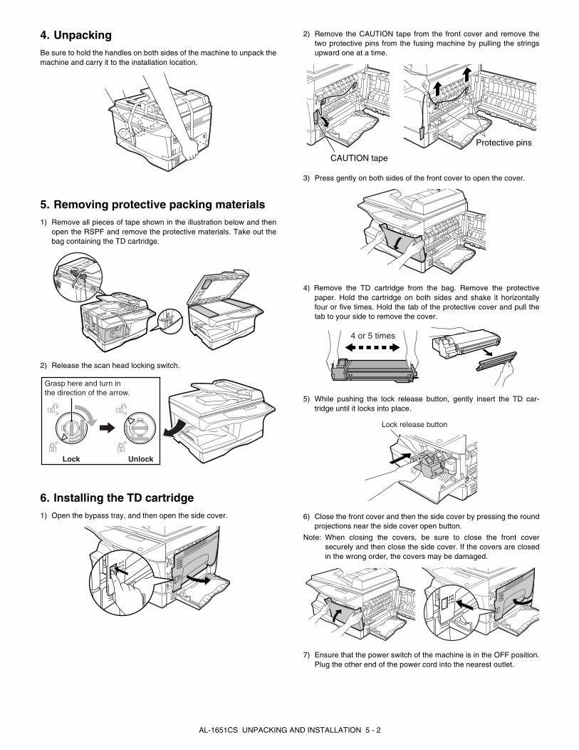
4. UnpackingBe sure to hold the handles on both sides of the machine to unpack themachine and carry it to the installation location.
5. Removing protective packing materials1) Remove all pieces of tape shown in the illustration below and then
open the RSPF and remove the protective materials. Take out thebag containing the TD cartridge.
2) Release the scan head locking switch.
6. Installing the TD cartridge1) Open the bypass tray, and then open the side cover.
2) Remove the CAUTION tape from the front cover and remove thetwo protective pins from the fusing machine by pulling the stringsupward one at a time.
3) Press gently on both sides of the front cover to open the cover.
4) Remove the TD cartridge from the bag. Remove the protectivepaper. Hold the cartridge on both sides and shake it horizontallyfour or five times. Hold the tab of the protective cover and pull thetab to your side to remove the cover.
5) While pushing the lock release button, gently insert the TD car-tridge until it locks into place.
6) Close the front cover and then the side cover by pressing the roundprojections near the side cover open button.
Note: When closing the covers, be sure to close the front coversecurely and then close the side cover. If the covers are closedin the wrong order, the covers may be damaged.
7) Ensure that the power switch of the machine is in the OFF position.Plug the other end of the power cord into the nearest outlet.
Lock Unlock
Grasp here and turn in the direction of the arrow.
CAUTION tape
Protective pins
4 or 5 times
Lock release button
AL-1651CS UNPACKING AND INSTALLATION 5 - 2

7. Loading the paper trayNote: Make sure that the paper is not torn, is free of dust, and has no
wrinkles or curled edges.
1) Raise the handle of the paper tray and pull the paper tray out until itstops.
2) Remove the pressure plate lock. Rotate the pressure plate lock inthe direction of the arrow to remove it while pressing down on thepressure plate of the paper tray.
3) Store the pressure plate lock which has been removed in step 2. Tostore the pressure plate lock, rotate the lock to secure it as shownbelow.
4) Squeeze the lock lever of the front guide and slide the front guide tomatch the width of the paper, and move the left guide to the appro-priate slot as marked on the tray.
• The front guide is a slide-type guide. Grasp the locking knob onthe guide and slide the guide to the indicator line of the paper tobe loaded.
• The left guide is an insert-type guide. Remove it and then insert itat the indicator line of the paper to be loaded.
5) Fan the paper and insert it into the tray. Make sure that the edgesgo under the corner hooks.
Note:
• Do not load paper above the maximum height line ( ).Exceeding the line will cause a paper misfeed.
• If the paper is not fanned, double-feeds or misfeeds may occur.
• Make sure the stack of paper is straight before loading it. When add-ing paper, take the remaining paper out and combine it into a singlestack with the new paper.
• Make sure that all the paper in the stack is the same size and type.
• When loading paper, ensure that there is no space between thepaper and the guide, and make sure that the guide is not set too nar-row and causes the paper to bend. Incorrect loading will cause thepaper to skew or misfeed.
6) Gently push the paper tray back into the machine.
Note:
• If you loaded a different size of paper than was loaded previously inthe tray.
• When not using the machine for an extended period, remove allpaper from the paper tray and store it in a dry place. If paper is left inthe machine for an extended period, the paper will absorb moisturefrom the air, resulting in paper jams.
8. Power to copier1) Ensure that the power switch of the copier is in the OFF position.
Insert the attached power cord into the power cord socket at therear of the copier.
2) Plug the other end of the power cord into the nearest outlet.
9. Software for AL-1651CSThe CD-ROM that accompanies the machine contains the followingsoftware:
MFP driverPrinter driver
The printer driver enables you to use the printer function of themachine.
The printer driver includes the Print Status Window. This is a utility thatmonitors the machine and informs you of the printing status, the nameof the document currently being printed, and error messages.
Please note that the Print Status Window does not operate when themachine is used as a network printer.
Scanner driver (USB only)
The scanner driver allows you to use the scanning function of themachine with TWAIN-compliant and WIA-compliant applications.
Sharpdesk (USB only)Sharpdesk is an integrated software environment that makes it easy tomanage documents and image files, and launch applications.
Button Manager (USB only)Button Manager allows you to use the scanner menus on the machineto scan a document.
Note: The scanning feature can only be used with computers that arerunning Windows 98/Me/2000/XP and are connected to themachine by a USB cable. If you are running Windows 95/NT 4.0or are connected to the machine by a LAN connection, only theprinter function can be used.
Pressure plate lock
Left guide
Front guide
AL-1651CS UNPACKING AND INSTALLATION 5 - 3
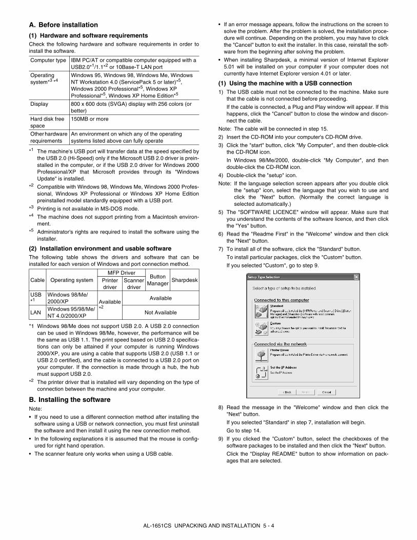
A. Before installation
(1) Hardware and software requirementsCheck the following hardware and software requirements in order toinstall the software.
*1 The machine's USB port will transfer data at the speed specified bythe USB 2.0 (Hi-Speed) only if the Microsoft USB 2.0 driver is prein-stalled in the computer, or if the USB 2.0 driver for Windows 2000Professional/XP that Microsoft provides through its "WindowsUpdate" is installed.
*2 Compatible with Windows 98, Windows Me, Windows 2000 Profes-sional, Windows XP Professional or Windows XP Home Editionpreinstalled model standardly equipped with a USB port.
*3 Printing is not available in MS-DOS mode.
*4 The machine does not support printing from a Macintosh environ-ment.
*5 Administrator's rights are required to install the software using theinstaller.
(2) Installation environment and usable softwareThe following table shows the drivers and software that can beinstalled for each version of Windows and port connection method.
*1 Windows 98/Me does not support USB 2.0. A USB 2.0 connectioncan be used in Windows 98/Me, however, the performance will bethe same as USB 1.1. The print speed based on USB 2.0 specifica-tions can only be attained if your computer is running Windows2000/XP, you are using a cable that supports USB 2.0 (USB 1.1 orUSB 2.0 certified), and the cable is connected to a USB 2.0 port onyour computer. If the connection is made through a hub, the hubmust support USB 2.0.
*2 The printer driver that is installed will vary depending on the type ofconnection between the machine and your computer.
B. Installing the softwareNote:
• If you need to use a different connection method after installing thesoftware using a USB or network connection, you must first uninstallthe software and then install it using the new connection method.
• In the following explanations it is assumed that the mouse is config-ured for right hand operation.
• The scanner feature only works when using a USB cable.
• If an error message appears, follow the instructions on the screen tosolve the problem. After the problem is solved, the installation proce-dure will continue. Depending on the problem, you may have to clickthe "Cancel" button to exit the installer. In this case, reinstall the soft-ware from the beginning after solving the problem.
• When installing Sharpdesk, a minimal version of Internet Explorer5.01 will be installed on your computer if your computer does notcurrently have Internet Explorer version 4.01 or later.
(1) Using the machine with a USB connection1) The USB cable must not be connected to the machine. Make sure
that the cable is not connected before proceeding.
If the cable is connected, a Plug and Play window will appear. If thishappens, click the "Cancel" button to close the window and discon-nect the cable.
Note: The cable will be connected in step 15.
2) Insert the CD-ROM into your computer's CD-ROM drive.
3) Click the "start" button, click "My Computer", and then double-clickthe CD-ROM icon.
In Windows 98/Me/2000, double-click "My Computer", and thendouble-click the CD-ROM icon.
4) Double-click the "setup" icon.
Note: If the language selection screen appears after you double clickthe "setup" icon, select the language that you wish to use andclick the "Next" button. (Normally the correct language isselected automatically.)
5) The "SOFTWARE LICENCE" window will appear. Make sure thatyou understand the contents of the software licence, and then clickthe "Yes" button.
6) Read the "Readme First" in the "Welcome" window and then clickthe "Next" button.
7) To install all of the software, click the "Standard" button.
To install particular packages, click the "Custom" button.
If you selected "Custom", go to step 9.
8) Read the message in the "Welcome" window and then click the"Next" button.
If you selected "Standard" in step 7, installation will begin.
Go to step 14.
9) If you clicked the "Custom" button, select the checkboxes of thesoftware packages to be installed and then click the "Next" button.
Click the "Display README" button to show information on pack-ages that are selected.
Computer type IBM PC/AT or compatible computer equipped with a USB2.0*1/1.1*2 or 10Base-T LAN port
Operating system*3 *4
Windows 95, Windows 98, Windows Me, Windows NT Workstation 4.0 (ServicePack 5 or later)*5, Windows 2000 Professional*5, Windows XP Professional*5, Windows XP Home Edition*5
Display 800 x 600 dots (SVGA) display with 256 colors (or better)
Hard disk free space
150MB or more
Other hardware requirements
An environment on which any of the operating systems listed above can fully operate
Cable Operating systemMFP Driver
Button Manager
SharpdeskPrinter driver
Scanner driver
USB*1
Windows 98/Me/2000/XP Available
*2
Available
LANWindows 95/98/Me/ NT 4.0/2000/XP
Not Available
AL-1651CS UNPACKING AND INSTALLATION 5 - 4
10) Check the packages on the screen, and then click the "Start" but-ton.
The software packages to be installed will be displayed on thescreen. If an incorrect package is displayed, click the "Back" but-ton and select the correct packages.
11) The files required for installation of the MFP driver are copied (if"MFP Driver" was selected).
Follow the on-screen instructions.
Caution: If you are running Windows 2000/XP and a warning messageappears regarding the Windows logo test or digital signature,be sure to click "Continue Anyway" or "Yes".
When "The installation of the SHARP software is complete"appears, click the "OK" button.
12) Begin the installation of Button Manager (if "Button Manager" wasselected).
Follow the on-screen instructions.
Click the "Finish" button when the message informs you that setupis successful.
The Sharpdesk installer will start.
13) Begin the installation of Sharpdesk (if "Sharpdesk" was selected).
Follow the on-screen instructions.
Click the "Finish" button when the message informs you thatSetup is complete.
Caution: In Windows 98/Me/2000, if the following screen appears,click the "Skip" button or the "Continue" button as appropriateto continue the Sharpdesk installation.
If "Skip" is selected, the Sharpdesk installation will continuewithout installing Sharpdesk Imaging.
If "Continue" is selected, Sharpdesk Imaging will be installed.If Imaging for Windows is installed on your computer, Sharp-desk
Imaging will overwrite Imaging for Windows.
14) When the "Finish" screen appears, click the "Close" button.
Caution: If you are running Windows 2000/XP and a warning messageappears regarding the Windows logo test or digital signature,be sure to click "Continue Anyway" or "Yes".
A message will appear instructing you to connect the machine toyour computer. Click the OK button.
Note:
• If this is a "Standard" installation, the "Finish" screen will appearafter several minutes.
• After the installation, a message prompting you to restart your com-puter may appear. In this case, click the "Yes" button to restart yourcomputer.
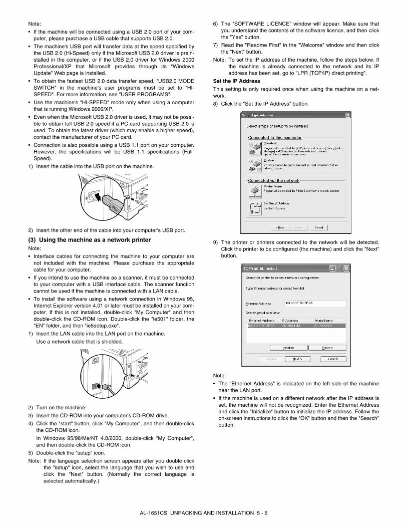
15) Make sure that the power of the machine is turned on, and thenconnect the USB cable.
Windows will detect the machine and a Plug and Play screen willappear.
Caution: If the following message appears on your computer screen,close it.
A window regarding "HI-SPEED USB Device" will thenappear. Close the window.
This message appears when the machine's USB 2.0 mode isnot set to "HI-SPEED". For information on switching the USB2.0 mode.
16) Begin installation of the scanner driver.
"SHARP AL-XXXXCS" will appear in the "Found New HardwareWizard" dialog box. Select "Install the software automatically(Recommended)" and click the "Next" button. Follow the on-screen instructions.
Caution: If you are running Windows 2000/XP and a warning messageappears regarding the Windows logo test or digital signature,be sure to click "Continue Anyway" or "Yes".
Note: A "USB 2.0 Composite Device" installation window may appearprior to this procedure. In this case, follow the instructions in thewindow to install the USB 2.0 Composite Device.
17) Begin installation of the printer driver.
"SHARP AL-XXXXCS" will appear in the "Found New HardwareWizard" dialog box. Select "Install the software automatically(Recommended)" and click the "Next" button. Follow the on-screen instructions.
Caution: If you are running Windows 2000/XP and a warning messageappears regarding the Windows logo test or digital signature,be sure to click "Continue Anyway" or "Yes".
18) Follow the instructions in the Plug and Play screen that appears inyour version of Windows to begin the installation.
This completes the installation of the software.
• If you installed Button Manager, set up Button Manager as explainedin "SETTING UP BUTTON MANAGER".
(2) Connecting a USB cableFollow the procedure below to connect the machine to your computer.
A USB cable for connecting the machine to your computer is notincluded with the machine. Please purchase the appropriate cable foryour computer.
Caution:
• USB is available with a PC/AT compatible computer that was origi-nally equipped with USB and had Windows 98, Windows Me, Win-dows 2000 Professional, Windows XP Professional or Windows XPHome Edition preinstalled.
• Do not connect the USB cable before installing the MFP driver. TheUSB cable should be connected during installation of the MFPdriver.
AL-1651CS UNPACKING AND INSTALLATION 5 - 5
Note:
• If the machine will be connected using a USB 2.0 port of your com-puter, please purchase a USB cable that supports USB 2.0.
• The machine's USB port will transfer data at the speed specified bythe USB 2.0 (Hi-Speed) only if the Microsoft USB 2.0 driver is prein-stalled in the computer, or if the USB 2.0 driver for Windows 2000Professional/XP that Microsoft provides through its "WindowsUpdate" Web page is installed.
• To obtain the fastest USB 2.0 data transfer speed, "USB2.0 MODESWITCH" in the machine's user programs must be set to "HI-SPEED". For more information, see "USER PROGRAMS".
• Use the machine's "HI-SPEED" mode only when using a computerthat is running Windows 2000/XP.
• Even when the Microsoft USB 2.0 driver is used, it may not be possi-ble to obtain full USB 2.0 speed if a PC card supporting USB 2.0 isused. To obtain the latest driver (which may enable a higher speed),contact the manufacturer of your PC card.
• Connection is also possible using a USB 1.1 port on your computer.However, the specifications will be USB 1.1 specifications (Full-Speed).
1) Insert the cable into the USB port on the machine.
2) Insert the other end of the cable into your computer's USB port.
(3) Using the machine as a network printerNote:
• Interface cables for connecting the machine to your computer arenot included with the machine. Please purchase the appropriatecable for your computer.
• If you intend to use the machine as a scanner, it must be connectedto your computer with a USB interface cable. The scanner functioncannot be used if the machine is connected with a LAN cable.
• To install the software using a network connection in Windows 95,Internet Explorer version 4.01 or later must be installed on your com-puter. If this is not installed, double-click "My Computer" and thendouble-click the CD-ROM icon. Double-click the "le501" folder, the"EN" folder, and then "ie5setup.exe".
1) Insert the LAN cable into the LAN port on the machine.
Use a network cable that is shielded.
2) Turn on the machine.
3) Insert the CD-ROM into your computer's CD-ROM drive.
4) Click the "start" button, click "My Computer", and then double-clickthe CD-ROM icon.
In Windows 95/98/Me/NT 4.0/2000, double-click "My Computer",and then double-click the CD-ROM icon.
5) Double-click the "setup" icon.
Note: If the language selection screen appears after you double clickthe "setup" icon, select the language that you wish to use andclick the "Next" button. (Normally the correct language isselected automatically.)
6) The "SOFTWARE LICENCE" window will appear. Make sure thatyou understand the contents of the software licence, and then clickthe "Yes" button.
7) Read the "Readme First" in the "Welcome" window and then clickthe "Next" button.
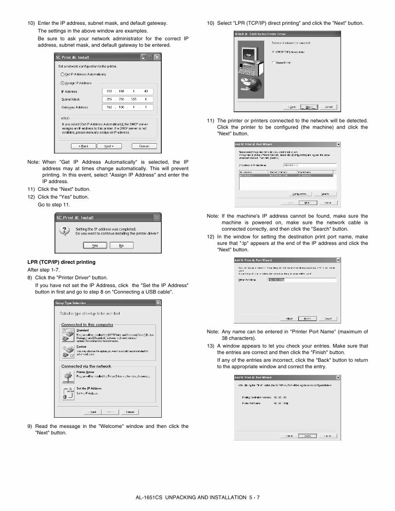
Note: To set the IP address of the machine, follow the steps below. Ifthe machine is already connected to the network and its IPaddress has been set, go to "LPR (TCP/IP) direct printing".
Set the IP Address
This setting is only required once when using the machine on a net-work.
8) Click the "Set the IP Address" button.
9) The printer or printers connected to the network will be detected.Click the printer to be configured (the machine) and click the "Next"button.
Note:
• The "Ethernet Address" is indicated on the left side of the machinenear the LAN port.
• If the machine is used on a different network after the IP address isset, the machine will not be recognized. Enter the Ethernet Addressand click the "Initialize" button to initialize the IP address. Follow theon-screen instructions to click the "OK" button and then the "Search"button.
AL-1651CS UNPACKING AND INSTALLATION 5 - 6
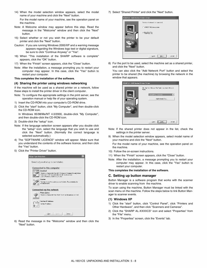
10) Enter the IP address, subnet mask, and default gateway.
The settings in the above window are examples.
Be sure to ask your network administrator for the correct IPaddress, subnet mask, and default gateway to be entered.
Note: When "Get IP Address Automatically" is selected, the IPaddress may at times change automatically. This will preventprinting. In this event, select "Assign IP Address" and enter theIP address.
11) Click the "Next" button.
12) Click the "Yes" button.
Go to step 11.
LPR (TCP/IP) direct printing
After step 1-7.
8) Click the "Printer Driver" button.
If you have not set the IP Address, click the "Set the IP Address"button in first and go to step 8 on "Connecting a USB cable".
9) Read the message in the "Welcome" window and then click the"Next" button.
10) Select "LPR (TCP/IP) direct printing" and click the "Next" button.
11) The printer or printers connected to the network will be detected.Click the printer to be configured (the machine) and click the"Next" button.
Note: If the machine's IP address cannot be found, make sure themachine is powered on, make sure the network cable isconnected correctly, and then click the "Search" button.
12) In the window for setting the destination print port name, makesure that ":lp" appears at the end of the IP address and click the"Next" button.
Note: Any name can be entered in "Printer Port Name" (maximum of38 characters).
13) A window appears to let you check your entries. Make sure thatthe entries are correct and then click the "Finish" button.
If any of the entries are incorrect, click the "Back" button to returnto the appropriate window and correct the entry.
AL-1651CS UNPACKING AND INSTALLATION 5 - 7
14) When the model selection window appears, select the modelname of your machine and click the "Next" button.
For the model name of your machine, see the operation panel onthe machine.
Note: A Welcome window may appear before this step. Read themessage in the "Welcome" window and then click the "Next"button.
15) Select whether or not you wish the printer to be your defaultprinter and click the "Next" button.
Caution: If you are running Windows 2000/XP and a warning messageappears regarding the Windows logo test or digital signature,be sure to click "Continue Anyway" or "Yes".
16) When "This installation of the SHARP software is complete"appears, click the "OK" button.
17) When the "Finish" screen appears, click the "Close" button.
Note: After the installation, a message prompting you to restart yourcomputer may appear. In this case, click the "Yes" button torestart your computer.
This completes the installation of the software.
(4) Sharing the printer using windows networkingIf the machine will be used as a shared printer on a network, followthese steps to install the printer driver in the client computer.
Note: To configure the appropriate settings in the print server, see theoperation manual or help file of your operating system.
1) Insert the CD-ROM into your computer's CD-ROM drive.
2) Click the "start" button, click "My Computer", and then double-clickthe CD-ROM icon.
In Windows 95/98/Me/NT 4.0/2000, double-click "My Computer",and then double-click the CD-ROM icon.
3) Double-click the "setup" icon.
Note: If the language selection screen appears after you double clickthe "setup" icon, select the language that you wish to use andclick the "Next" button. (Normally the correct language isselected automatically.)
4) The "SOFTWARE LICENCE" window will appear. Make sure thatyou understand the contents of the software licence, and then clickthe "Yes" button.
5) Click the "Printer Driver" button.
6) Read the message in the "Welcome" window and then click the"Next" button.
7) Select "Shared Printer" and click the "Next" button.
8) For the port to be used, select the machine set as a shared printer,and click the "Next" button.
You can also click the "Add Network Port" button and select theprinter to be shared (the machine) by browsing the network in thewindow that appears.
Note: If the shared printer does not appear in the list, check thesettings in the printer server.
9) When the model selection window appears, select model name ofyour machine and click the "Next" button.
For the model name of your machine, see the operation panel onthe machine.
10) Follow the on-screen instructions.
11) When the "Finish" screen appears, click the "Close" button.
Note: After the installation, a message prompting you to restart yourcomputer may appear. In this case, click the "Yes" button torestart your computer.
This completes the installation of the software.
C. Setting up button managerButton Manager is a software program that works with the scannerdriver to enable scanning from the machine.
To scan using the machine, Button Manager must be linked with thescan menu on the machine. Follow the steps below to link Button Man-ager to scanner events.
(1) Windows XP1) Click the "start" button, click "Control Panel", click "Printers and
Other Hardware", and then click "Scanners and Cameras".
2) Click the "SHARP AL-XXXXCS" icon and select "Properties" fromthe "File" menu.
3) In the "Properties" screen, click the "Events" tab.
AL-1651CS UNPACKING AND INSTALLATION 5 - 8

4) Select "SC1:" from the "Select an event" pull-down menu.
5) Select "Start this program" and then select "Sharp Button ManagerB" from the pull-down menu.
6) Click the "Apply" button.
7) Repeat Steps 4 through 6 to link Button Manager to "SC2:" through"SC6:".
Select "SC2:" from the "Select an event" pull-down menu. Select"Start this program", select "Sharp Button Manager B" from the pull-down menu, and then click the "Apply" button. Do the same foreach ScanMenu through "SC6:".
When the settings have been completed, click the "OK" button toclose the screen.
Button Manager is now linked to the scan menu (1 through 6).
The scan settings for each of scan menu 1 through 6 can be changedwith the setting window of Button Manager.
For the factory default settings of the scan menu. For the proceduresfor configuring Button Manager settings, see "Button Manager Set-tings" in the Online Manual.
(2) Windows 98/Me/20001) click the "Start" button, select "Settings", and then click "Control
Panel".
2) Double-click the "Scanners and Cameras" icon.
Note: If the "Scanners and Cameras" icon does not appear inWindows Me, click "view all Control Panel options".
3) Select "SHARP AL-XXXXCS" and click the "Properties" button.
In Windows Me, right click "SHARP AL-XXXXCS" and click "Prop-erties" in the pop-up menu.
4) In the "Properties" screen, click the "Events" tab.
5) Select "SC1:" from the "Scanner events" pull-down menu.
6) Select "Sharp Button Manager B" in "Send to this application".
Note: If other applications are shown, deselect the checkboxes for theother applications and leave only the Button Manager checkboxselected.
7) Click the "Apply" button.
8) Repeat Steps 5 through 7 to link Button Manager to "SC2:" through"SC6:".
Select "SC2:" from the "Scanner events" pull-down menu. Select"Sharp Button Manager B" in "Send to this application" and click the"Apply" button. Do the same for each ScanMenu through "SC6:".
When the settings have been completed, click the "OK" button toclose the screen.
Button Manager is now linked to the scan menu (1 through 6).
The scan settings for each of scan menus 1 through 6 can be changedwith the setting window of Button Manager.
For the factory default settings of the scan menu. For the proceduresfor configuring Button Manager settings, see "Button Manager Set-tings" in the Online Manual.
AL-1651CS UNPACKING AND INSTALLATION 5 - 9

10. Interface
A. USB
Connector4-pin ACON UBR23-4K2200
Type-B connector
CableShielded twisted pair cable
(2 m (6 feet) Max.: high-speed transmission equivalent)
Pin configurationThe pin numbers and signal names are listed in the following table.
11. Moving
Moving instructionsWhen moving the unit, follow the procedure below.
Note: When moving this unit, be sure to remove the TD cartridge inadvance.
1) Turn the power switch off and remove the power cord from the out-let.
2) Open the side cover and front cover, in that order. Remove the TDcartridge and close the front cover and side cover, in that order.
To open and close the side cover and front cover, and to removethe TD cartridge.
3) Raise the handle of the paper tray and pull the paper tray out until itstops.
4) Push the center of the pressure plate down until it locks in placeand lock the plate using the pressure plate lock which has beenstored in the front of the paper tray.
5) Push the paper tray back into the unit.
6) Lock the scan head locking switch.
Note: When shipping the unit, the scan head locking switch must belocked to prevent shipping damage.
7) Close the multi-bypass tray and the paper output tray extension,and attach the packing materials and tape which were removedduring installation of the unit.
8) Pack the unit into the carton.
B. RJ45RJ-45 connector pin arrangement
Pin No. Signal name1 +5V2 -DATA3 +DATA4 GND
12
3 4
Pin No. Signal name LAN adapter RJ-45 connector1 TD+ Send output +2 TD– Send output -3 RD+ Receive input +6 RD– Receive input -
4, 5, 7, 8 Not used. Not used.
1 8
AL-1651CS UNPACKING AND INSTALLATION 5 - 10
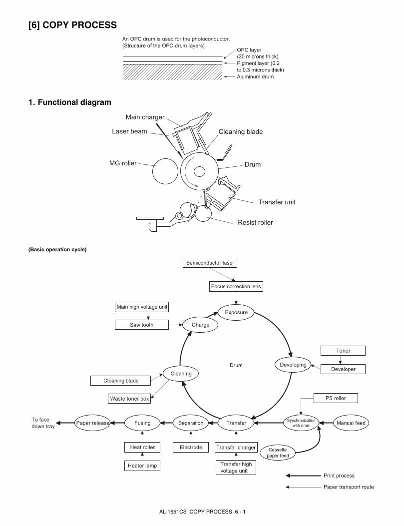
[6] COPY PROCESS
1. Functional diagram
(Basic operation cycle)
(20 microns thick)
Aluminum drum
Pigment layer (0.2to 0.3 microns thick)
An OPC drum is used for the photoconductor.(Structure of the OPC drum layers)
OPC layer
Main charger
Laser beam
MG roller
Cleaning blade
Drum
Transfer unit
Resist roller
ExposureMain high voltage unit
Saw tooth Charge
Drum
CleaningCleaning blade
Waste toner box
Paper release Fusing Separation
Heat roller
Heater lamp
Transfer
Transfer charger
Transfer highvoltage unit
Developing
Toner
Developer
Print process
Paper transport route
Semiconductor laser
Manual feed
PS roller
Focus correction lens
Electrode
Synchronizationwith drum
Cassettepaper feed
To facedown tray
AL-1651CS COPY PROCESS 6 - 1

2. Outline of print processThis printer is a non-impact printer that uses a semiconductor laserand electrostatic print process. This printer uses an OPC (OrganicPhoto Conductor) for its photoconductive material.First, voltage from the main corona unit charges the drum surface anda latent image is formed on the drum surface using a laser beam. Thislatent image forms a visible image on the drum surface when toner isapplied. The toner image is then transferred onto the print paper by thetransfer corona and fused on the print paper in the fusing section witha combination of heat and pressure.
Step-1: ChargeStep-2: Exposure* Latent image is formed on the drum.Step-3: Developing
Latent image formed on the drum is then changed into visibleimage with toner.
Step-4: TransferThe visible image (toner image) on the drum is transferredonto the print paper.
Step-5: CleaningResidual toner on the drum surface is removed and collectedby the cleaning blade.
Step-6: Optical dischargeResidual charge on the drum surface is removed, bysemiconductor laser beam.
3. Actual print processStep-1: DC charge
A uniform negative charge is applied over the OPC drum surface bythe main charging unit. Stable potential is maintained by means of theScorotron charger. Positive charges are generated in the aluminum layer.
Step-2: Exposure (laser beam, lens)
A Laser beam is generated from the semiconductor laser andcontrolled by the print pattern signal. The laser writes onto the OPCdrum surface through the polygon mirrors and lens. The resistance ofthe OPC layer decreases for an area exposed by the laser beam(corresponding to the print pattern signal). The beam neutralizes thenegative charge. An electrostatic latent image is formed on the drumsurface.
AboutDC5.5KV
( 580V/ 400V)
OPC layerPigmentlayerAluminumdrum
OPC layerPigmentlayerAluminumlayer
Drum surface chargeafter the exposure
Non-image area Image area
Semiconductor laser
Exposure(semiconductor laser)
AL-1651CS COPY PROCESS 6 - 2
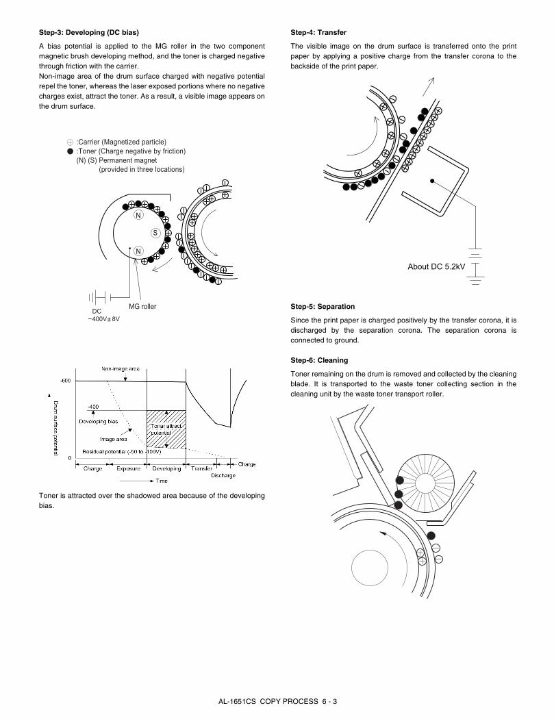
Step-3: Developing (DC bias)
A bias potential is applied to the MG roller in the two componentmagnetic brush developing method, and the toner is charged negativethrough friction with the carrier.Non-image area of the drum surface charged with negative potentialrepel the toner, whereas the laser exposed portions where no negativecharges exist, attract the toner. As a result, a visible image appears onthe drum surface.
Toner is attracted over the shadowed area because of the developingbias.
Step-4: Transfer
The visible image on the drum surface is transferred onto the printpaper by applying a positive charge from the transfer corona to thebackside of the print paper.
Step-5: Separation
Since the print paper is charged positively by the transfer corona, it isdischarged by the separation corona. The separation corona isconnected to ground.
Step-6: Cleaning
Toner remaining on the drum is removed and collected by the cleaningblade. It is transported to the waste toner collecting section in thecleaning unit by the waste toner transport roller.
S
N
N
:Carrier (Magnetized particle):Toner (Charge negative by friction)(N) (S) Permanent magnet
(provided in three locations)
MG roller
DC400V 8V
About DC 5.2kV
AL-1651CS COPY PROCESS 6 - 3
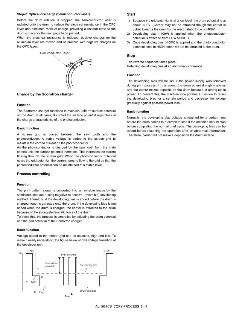
Step-7: Optical discharge (Semiconductor laser)
Before the drum rotation is stopped, the semiconductor laser isradiated onto the drum to reduce the electrical resistance in the OPClayer and eliminate residual charge, providing a uniform state to thedrum surface for the next page to be printed.When the electrical resistance is reduced, positive charges on thealuminum layer are moved and neutralized with negative charges onthe OPC layer.
Charge by the Scorotron charger
Function
The Scorotron charger functions to maintain uniform surface potentialon the drum at all times, It control the surface potential regardless ofthe charge characteristics of the photoconductor.
Basic function
A screen grid is placed between the saw tooth and thephotoconductor. A stable voltage is added to the screen grid tomaintain the corona current on the photoconductor.As the photoconductor is charged by the saw tooth from the maincorona unit, the surface potential increases. This increases the currentflowing through the screen grid. When the photoconductor potentialnears the grid potential, the current turns to flow to the grid so that thephotoconductor potential can be maintained at a stable level.
Process controlling
Function
The print pattern signal is converted into an invisible image by thesemiconductor laser using negative to positive (reversible) developingmethod. Therefore, if the developing bias is added before the drum ischarged, toner is attracted onto the drum. If the developing bias is notadded when the drum is charged, the carrier is attracted to the drumbecause of the strong electrostatic force of the drum.To avoid this, the process is controlled by adjusting the drum potentialand the grid potential of the Scorotron charger.
Basic function
Voltage added to the screen grid can be selected, high and low. Tomake it easily understood, the figure below shows voltage transition atthe developer unit.
Start
1) Because the grid potential is at a low level, the drum potential is atabout -400V. (Carrier may not be attracted though the carrier ispulled towards the drum by the electrostatic force of -400V.
2) Developing bias (-400V) is applied when the photoconductorpotential is switched from LOW to HIGH.
3) Once developing bias (-400V) is applied and the photo conductorpotential rises to HIGH, toner will not be attracted to the drum.
Stop
The reverse sequence takes place.Retaining developing bias at an abnormal occurrence
Function
The developing bias will be lost if the power supply was removedduring print process. In this event, the drum potential slightly abatesand the carrier makes deposits on the drum because of strong staticpower. To prevent this, the machine incorporates a function to retainthe developing bias for a certain period and decrease the voltagegradually against possible power loss.
Basic function
Normally, the developing bias voltage is retained for a certain timebefore the drum comes to a complete stop if the machine should stopbefore completing the normal print cycle. The developing bias can beadded before resuming the operation after an abnormal interruption.Therefore, carrier will not make a deposit on the drum surface.
Semiconductor laser
0START STOP
Print potential
Toner attractpotential
2)
3)
1) Low
4) High Drum potential
Developing bias
Time
AL-1651CS COPY PROCESS 6 - 4
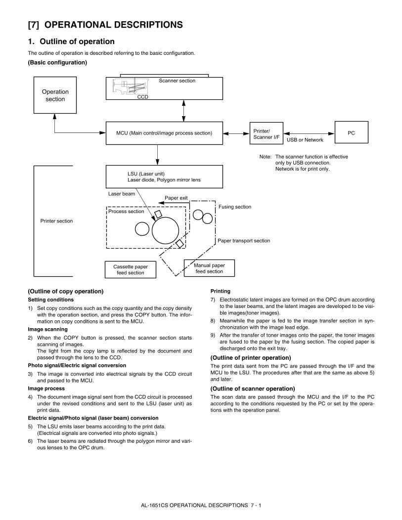
[7] OPERATIONAL DESCRIPTIONS
1. Outline of operationThe outline of operation is described referring to the basic configuration.
(Basic configuration)
(Outline of copy operation)Setting conditions
1) Set copy conditions such as the copy quantity and the copy densitywith the operation section, and press the COPY button. The infor-mation on copy conditions is sent to the MCU.
Image scanning
2) When the COPY button is pressed, the scanner section startsscanning of images. The light from the copy lamp is reflected by the document andpassed through the lens to the CCD.
Photo signal/Electric signal conversion
3) The image is converted into electrical signals by the CCD circuitand passed to the MCU.
Image process
4) The document image signal sent from the CCD circuit is processedunder the revised conditions and sent to the LSU (laser unit) asprint data.
Electric signal/Photo signal (laser beam) conversion
5) The LSU emits laser beams according to the print data.(Electrical signals are converted into photo signals.)
6) The laser beams are radiated through the polygon mirror and vari-ous lenses to the OPC drum.
Printing
7) Electrostatic latent images are formed on the OPC drum accordingto the laser beams, and the latent images are developed to be visi-ble images(toner images).
8) Meanwhile the paper is fed to the image transfer section in syn-chronization with the image lead edge.
9) After the transfer of toner images onto the paper, the toner imagesare fused to the paper by the fusing section. The copied paper isdischarged onto the exit tray.
(Outline of printer operation)The print data sent from the PC are passed through the I/F and theMCU to the LSU. The procedures after that are the same as above 5)and later.
(Outline of scanner operation)The scan data are passed through the MCU and the I/F to the PCaccording to the conditions requested by the PC or set by the opera-tions with the operation panel.
Operationsection
Scanner section
CCD
MCU (Main control/image process section) Printer/Scanner I/F USB or Network
PC
Note: The scanner function is effectiveonly by USB connection.Network is for print only.
Laser beamPaper exit
Fusing section
Paper transport section
Manual paperfeed section
Cassette paperfeed section
Printer section
LSU (Laser unit)Laser diode, Polygon mirror lens
Process section
AL-1651CS OPERATIONAL DESCRIPTIONS 7 - 1

2. Scanner sectionA. Scanner unitThe scanner unit in the digital copier scans images.
It is composed of the optical unit and the drive unit. The optical unitperforms scanning in the main scan direction with the light receivingelements (color CCD). The drive unit performs scanning in the subscanning direction by moving the optical unit.
B. Optical systemTwo white lamps are used as the light source.
Light radiated from the light source is applied to the document on thedocument table. The reflected light from the document is reflected 5times by No. 1 - No. 3 mirrors and passed through the reduction lens toform images on the light-receiving surface of 3-line CCD.
The light-receiving surface of the color CCD is provided with 3 linescanning sections for RGB. Separate images scanned in each colorsection are overlapped to complete color scanning. (When PC scan-ning)
The resolution is 600dpi.
When copying, only the green component is used to print with theprinter.
The color component for printing can be switched to red or blue by theservice test command.
(Spectrum characteristics of the lamp)
(Spectrum characteristics of the color CCD)
(Optical unit)
C. Drive systemThe drive system is composed of the scanner motor, the pulley gear,the idle pulley, the idle gear, the belt 473, the belt 190, and the shaft.
The motor rotation is converted into reciprocated movements of thebelt 473 through the idle gear, the pulley gear, the belt 190, and theidle pulley to drive the optical unit.
MBVM26W25W260NLH/G
0.00E+00
1.00E-01
2.00E-01
3.00E-01
4.00E-01
5.00E-01
6.00E-01
0 200 400 600 800Wave length (nm)
Inte
nsity
of U
V
Lamp : MBVM26W25W260NLH/GLamp current : 5mATemp. : 25 degree
1 Table glass 2 Optical unit 3 Lens4 Mirror 1 5 Mirror 2 6 Mirror 37 CCD PWB 8 Lamp 9 Reflector
1
98
10 8
9
7
35 4
2
6
1 Scanner motor 2 Pulley gear 3 Idle pulley4 Belt 473 5 Belt 190 6 Optical unit7 Shaft 8 Idle gear 9
7
3 4 6 2 8 5
1
3
AL-1651CS OPERATIONAL DESCRIPTIONS 7 - 2
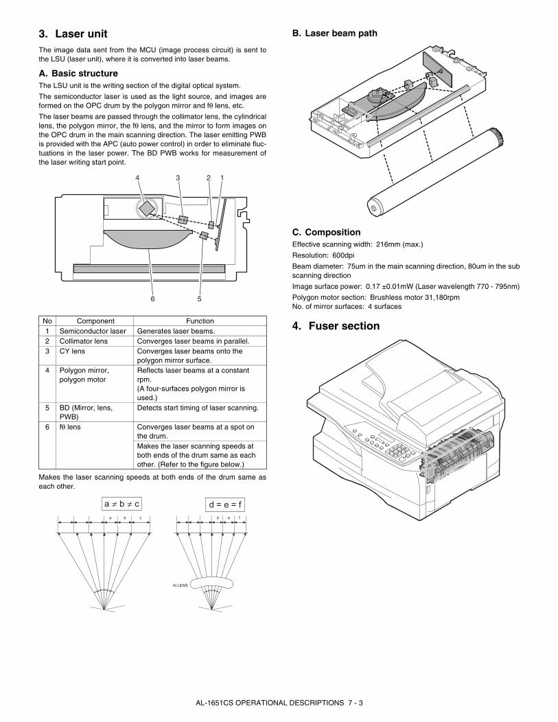
3. Laser unitThe image data sent from the MCU (image process circuit) is sent tothe LSU (laser unit), where it is converted into laser beams.
A. Basic structureThe LSU unit is the writing section of the digital optical system.
The semiconductor laser is used as the light source, and images areformed on the OPC drum by the polygon mirror and fθ lens, etc.
The laser beams are passed through the collimator lens, the cylindricallens, the polygon mirror, the fθ lens, and the mirror to form images onthe OPC drum in the main scanning direction. The laser emitting PWBis provided with the APC (auto power control) in order to eliminate fluc-tuations in the laser power. The BD PWB works for measurement ofthe laser writing start point.
Makes the laser scanning speeds at both ends of the drum same aseach other.
B. Laser beam path
C. CompositionEffective scanning width: 216mm (max.)
Resolution: 600dpi
Beam diameter: 75um in the main scanning direction, 80um in the subscanning direction
Image surface power: 0.17 ±0.01mW (Laser wavelength 770 - 795nm)
Polygon motor section: Brushless motor 31,180rpmNo. of mirror surfaces: 4 surfaces
4. Fuser sectionNo Component Function1 Semiconductor laser Generates laser beams.2 Collimator lens Converges laser beams in parallel.3 CY lens Converges laser beams onto the
polygon mirror surface. 4 Polygon mirror,
polygon motorReflects laser beams at a constant rpm.(A four-surfaces polygon mirror is used.)
5 BD (Mirror, lens, PWB)
Detects start timing of laser scanning.
6 fθ lens Converges laser beams at a spot on the drum.Makes the laser scanning speeds at both ends of the drum same as each other. (Refer to the figure below.)
2
5
3
6
4 1
a ≠ b ≠ ca b c
d = e = fd e f
fθ LENS
AL-1651CS OPERATIONAL DESCRIPTIONS 7 - 3

A. General descriptionGeneral block diagram (cross section)
Top view
(1) Heat rollerA Teflon roller is used for the heat roller and a silicone rubber roller isused for the lower heat roller for better toner fusing performance andpaper separation.
(2) Separator pawlThree separator pawls are used on the upper heat roller. The separa-tor pawls are Teflon coated to reduce friction with the roller and preventa smear on the paper caused by the separator pawl.
(3) Thermal control1) The heater lamp, thermistor, main PWB, DC power supply PWB,
and triac within the power supply unit are used to control thetemperature in the fuser unit.To prevent against abnormally high temperature in the fuser unit, athermal breaker and thermal fuse are used for safety purposes.
2) The surface temperature of the upper heat roller is set to 165 -190°C. The surface temperature during the power save mode isset to 100°C.
3) The self-check function comes active when one of the followingmalfunctions occurs, and an "H" is displayed on the multicopywindow.
a. When the heat roller surface temperature rises above 240°C.
b. When the heat roller surface temperature drops below 100°C duringthe copy cycle.
c. Open thermistor
d. Open thermal fuse
e. When the heat roller temperature does not reach 190°C within 27second after supplying the power.
(4) Fusing resistorFusing resistor
This model is provided with a fusing resistor in the fusing section toimprove transfer efficiency.
Since the upper heat roller is conductive, when using copy paper thatcontains moisture and the distance between the transfer unit and thefusing unit is short, the transfer current may find a path to ground viathe copy paper, the upper heat roller and the discharging brush.
5. Paper feed section and paper transport section
A. Paper transport path and general operations
Paper feed is made in two ways; the tray paper feed and the manualpaper feed. The tray is of universal-type, and has the capacity of 250sheets.
The front loading system allows you to install or remove the tray fromthe front cabinet.
The general descriptions on the tray paper feed and the manual paperfeed operation are given below.
Separator pawl
PPD2
Thermal fuse
Thermistor
Heat roller
Paper guide
Pressure roller
Heat rollerThermistor
Thermal fuse
Heater lamp
Separator pawl
Safety device(thermal breaker, thermalfuse)
Triac (in thepower supply unit)
Heated by the heater lamp. (950W)
The surface temperatureof the upper heat roller issensed by the thermistor.
Level of the thermistor iscontrolled by the main PWB.
With the signal from themain PWB, the triac iscontrolled on and off.(power supply PWB)
1 Scanner unit 8 Drum
2 Copy lamp 9 Transfer unit
3 LSU (Laser unit) 10 Pickup roller4 Paper exit roller 11 Manual paper feed tray
5 Main charger 12 Manual paper feed roller
6 Heat roller 13 PS roller unit
7 Pressure roller 14 Paper feed roller
1
2534
6
78910
11121314
AL-1651CS OPERATIONAL DESCRIPTIONS 7 - 4
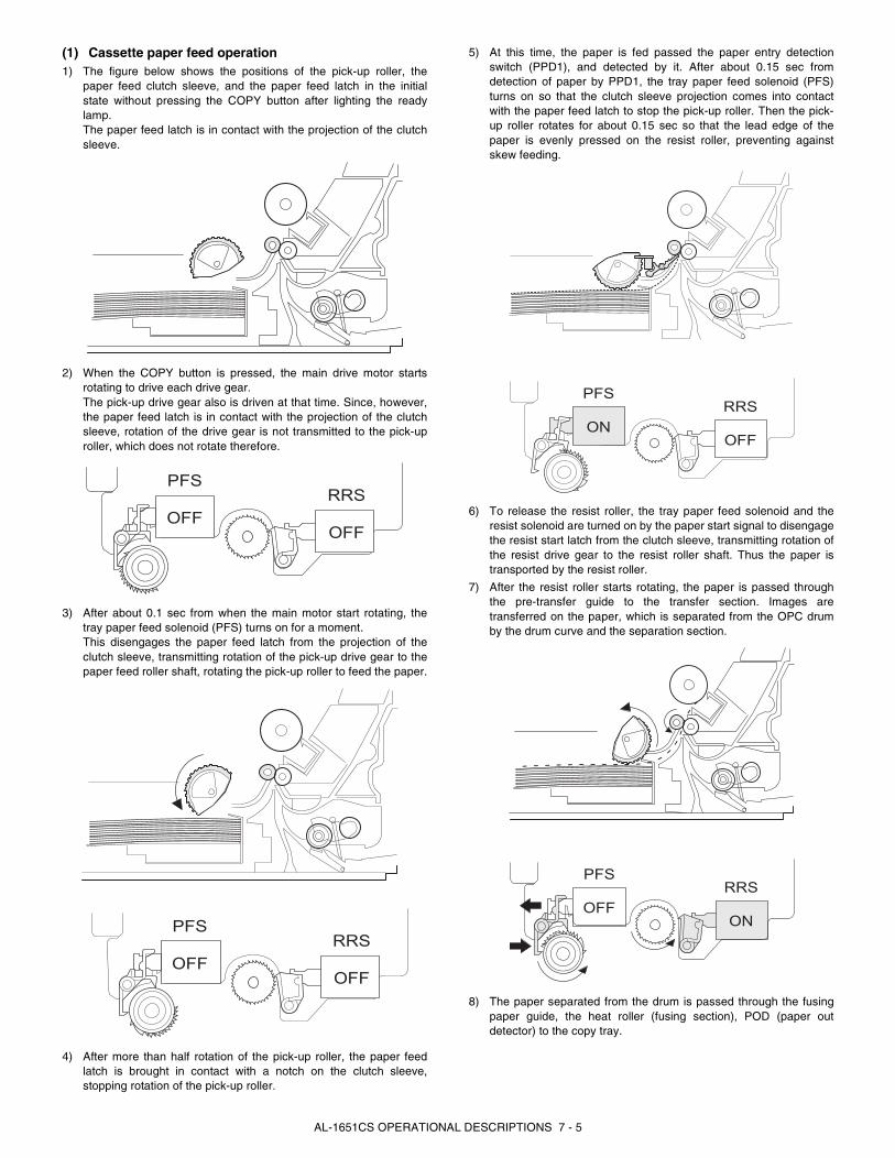
(1) Cassette paper feed operation1) The figure below shows the positions of the pick-up roller, the
paper feed clutch sleeve, and the paper feed latch in the initialstate without pressing the COPY button after lighting the readylamp.The paper feed latch is in contact with the projection of the clutchsleeve.
2) When the COPY button is pressed, the main drive motor startsrotating to drive each drive gear.The pick-up drive gear also is driven at that time. Since, however,the paper feed latch is in contact with the projection of the clutchsleeve, rotation of the drive gear is not transmitted to the pick-uproller, which does not rotate therefore.
3) After about 0.1 sec from when the main motor start rotating, thetray paper feed solenoid (PFS) turns on for a moment.This disengages the paper feed latch from the projection of theclutch sleeve, transmitting rotation of the pick-up drive gear to thepaper feed roller shaft, rotating the pick-up roller to feed the paper.
4) After more than half rotation of the pick-up roller, the paper feedlatch is brought in contact with a notch on the clutch sleeve,stopping rotation of the pick-up roller.
5) At this time, the paper is fed passed the paper entry detectionswitch (PPD1), and detected by it. After about 0.15 sec fromdetection of paper by PPD1, the tray paper feed solenoid (PFS)turns on so that the clutch sleeve projection comes into contactwith the paper feed latch to stop the pick-up roller. Then the pick-up roller rotates for about 0.15 sec so that the lead edge of thepaper is evenly pressed on the resist roller, preventing againstskew feeding.
6) To release the resist roller, the tray paper feed solenoid and theresist solenoid are turned on by the paper start signal to disengagethe resist start latch from the clutch sleeve, transmitting rotation ofthe resist drive gear to the resist roller shaft. Thus the paper istransported by the resist roller.
7) After the resist roller starts rotating, the paper is passed throughthe pre-transfer guide to the transfer section. Images aretransferred on the paper, which is separated from the OPC drumby the drum curve and the separation section.
8) The paper separated from the drum is passed through the fusingpaper guide, the heat roller (fusing section), POD (paper outdetector) to the copy tray.
OFF
PFS
OFF
RRS
OFF
PFS
OFF
RRS
ON
PFS
OFF
RRS
OFF
PFS
ON
RRS
AL-1651CS OPERATIONAL DESCRIPTIONS 7 - 5
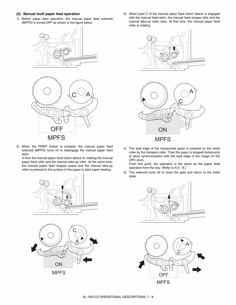
(2) Manual multi paper feed operation1) Before paper feed operation, the manual paper feed solenoid
(MPFS) is turned OFF as shown in the figure below.
2) When the PRINT button is pressed, the manual paper feedsolenoid (MPFS) turns on to disengage the manual paper feedlatch.A from the manual paper feed clutch sleeve A, rotating the manualpaper feed roller and the manual take-up roller. At the same time,the manual paper feed stopper opens and the manual take-uproller is pressed to the surface of the paper to start paper feeding.
3) When pawl C of the manual paper feed clutch sleeve is engagedwith the manual feed latch, the manual feed stopper falls and themanual take-up roller rises. At that time, the manual paper feedroller is rotating.
4) The lead edge of the transported paper is pressed on the resistroller by the transport roller. Then the paper is stopped temporarilyto allow synchronization with the lead edge of the image on theOPC drum.From this point, the operation is the same as the paper feedoperation from the tray. (Refer to A-5 - 8.)
5) The solenoid turns off to close the gate and return to the initialstate.
OFMPFS
F
C A
ON
MPFS
A
C
ON
MPFS
A
C
OF
MPFS
F
A
C
AL-1651CS OPERATIONAL DESCRIPTIONS 7 - 6
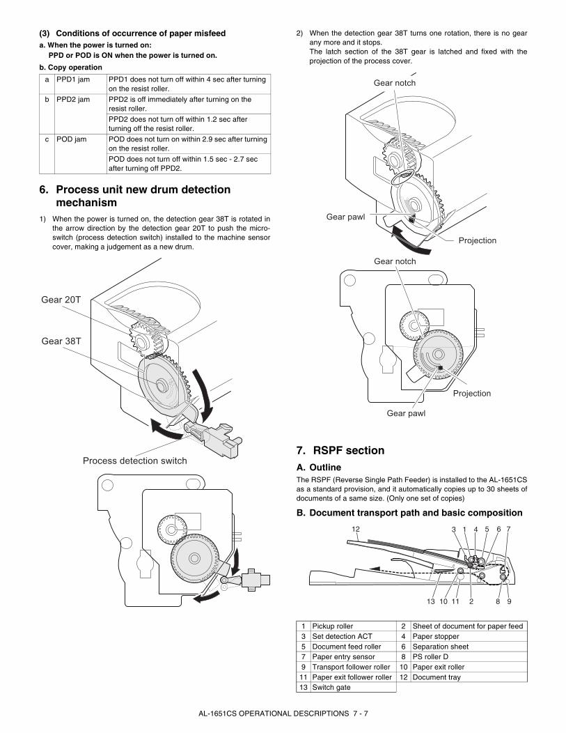
(3) Conditions of occurrence of paper misfeeda. When the power is turned on:
PPD or POD is ON when the power is turned on.
b. Copy operation
6. Process unit new drum detection mechanism
1) When the power is turned on, the detection gear 38T is rotated inthe arrow direction by the detection gear 20T to push the micro-switch (process detection switch) installed to the machine sensorcover, making a judgement as a new drum.
2) When the detection gear 38T turns one rotation, there is no gearany more and it stops.The latch section of the 38T gear is latched and fixed with theprojection of the process cover.
7. RSPF sectionA. OutlineThe RSPF (Reverse Single Path Feeder) is installed to the AL-1651CSas a standard provision, and it automatically copies up to 30 sheets ofdocuments of a same size. (Only one set of copies)
B. Document transport path and basic composition
a PPD1 jam PPD1 does not turn off within 4 sec after turning on the resist roller.
b PPD2 jam PPD2 is off immediately after turning on the resist roller.
PPD2 does not turn off within 1.2 sec after turning off the resist roller.
c POD jam POD does not turn on within 2.9 sec after turning on the resist roller.
POD does not turn off within 1.5 sec - 2.7 sec after turning off PPD2.
Gear 20T
Process detection switch
Gear 38T
1 Pickup roller 2 Sheet of document for paper feed3 Set detection ACT 4 Paper stopper5 Document feed roller 6 Separation sheet7 Paper entry sensor 8 PS roller D9 Transport follower roller 10 Paper exit roller
11 Paper exit follower roller 12 Document tray13 Switch gate
Gear notch
Gear pawl
Projection
Gear notch
Gear pawl
Projection
1 43 5 6 712
8 921113 10
AL-1651CS OPERATIONAL DESCRIPTIONS 7 - 7
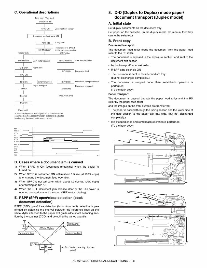
C. Operational descriptions
D. Cases where a document jam is caused1) When SPPD is ON (document remaining) when the power is
turned on.
2) When SPPD is not turned ON within about 1.5 sec (at 100% copy)after starting the document feed operation.
3) When SPPD is not turned on within about 4.7 sec (at 100% copy)after turning on SPPD.
4) When the SPF document jam release door or the OC cover isopened during document transport (SPF motor rotating).
E. RSPF (SPF) open/close detection (book document detection)
RSPF (SPF) open/close detection (book document) detection is per-formed by detecting the interval between the reference lines on thewhite Mylar attached to the paper exit guide (document scanning sec-tion) by the scanner (CCD) and detecting the varied quantity.
8. D-D (Duplex to Duplex) mode paper/document transport (Duplex model)
A. Initial stateSet duplex documents on the document tray.
Set paper on the cassette. (In the duplex mode, the manual feed traycannot be selected.)
B. Front copyDocument transport:
The document feed roller feeds the document from the paper feedroller to the PS roller.
• The document is exposed in the exposure section, and sent to thedocument exit section
• by the transport/paper exit roller.
• R-SPF gate solenoid ON
• The document is sent to the intermediate tray.(but not discharged completely.)
• The document is stopped once, then switchback operation isperformed. (To the back copy)
Paper transport:
The document is passed through the paper feed roller and the PSroller by the paper feed roller
and the images on the front surface are transferred.
• The paper is passed through the fusing section and the lower side ofthe gate section to the paper exit tray side, (but not dischargedcompletely.)
• It is stopped once and switchback operation is performed.(To the back copy)
SPID ON
PSW ON
MIRM rotation
MM rotation
CPFS ON
SPFM rotation
SPUS ON
Document set
Document set sensor
Document feed unit lamp ON
PPD ON
RRC ON SPPD ON
POD ON
Copy start
The scanner is shiftedto the exposure position.
(Copier side)
Main motor rotation
Paper feed
Synchronization
(Transfer)
(Fusing) (Document exit)
Paper transport
(Exposure)
In the zooming mode, the magnification ratio in the sub scanning direction (paper transport direction) is adjustedby changing the document transport speed.
(Paper exit)
SPF motor rotation
Document feed
Document transport sensor
Document transport
(SPF side)
Time chart (Tray feed)
752msec
625msec
756msec
PSW
MIRR M
SPF M
CL
SPUSSPPD
SCANST
MAIN M
CPFS1
RRSPPD1
PPD2
POD
BA
B
AA - B = Varied quantity of pixels
(pixel)
(Floating)
(White Mylar)
(CCD)
Reference line Reference line
AL-1651CS OPERATIONAL DESCRIPTIONS 7 - 8
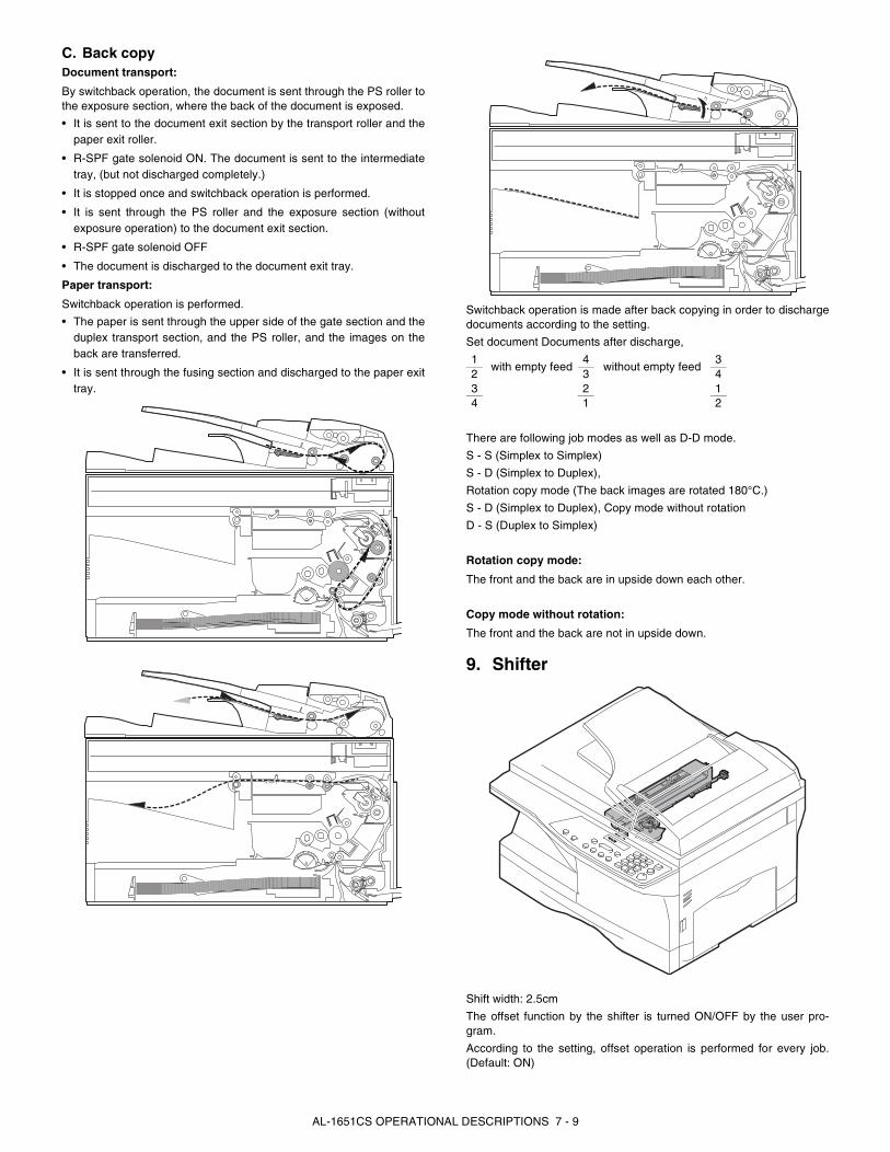
C. Back copyDocument transport:
By switchback operation, the document is sent through the PS roller tothe exposure section, where the back of the document is exposed.
• It is sent to the document exit section by the transport roller and thepaper exit roller.
• R-SPF gate solenoid ON. The document is sent to the intermediatetray, (but not discharged completely.)
• It is stopped once and switchback operation is performed.
• It is sent through the PS roller and the exposure section (withoutexposure operation) to the document exit section.
• R-SPF gate solenoid OFF
• The document is discharged to the document exit tray.
Paper transport:
Switchback operation is performed.
• The paper is sent through the upper side of the gate section and theduplex transport section, and the PS roller, and the images on theback are transferred.
• It is sent through the fusing section and discharged to the paper exittray.
Switchback operation is made after back copying in order to dischargedocuments according to the setting.
Set document Documents after discharge,
There are following job modes as well as D-D mode.
S - S (Simplex to Simplex)
S - D (Simplex to Duplex),
Rotation copy mode (The back images are rotated 180°C.)
S - D (Simplex to Duplex), Copy mode without rotation
D - S (Duplex to Simplex)
Rotation copy mode:
The front and the back are in upside down each other.
Copy mode without rotation:
The front and the back are not in upside down.
9. Shifter
Shift width: 2.5cm
The offset function by the shifter is turned ON/OFF by the user pro-gram.
According to the setting, offset operation is performed for every job.(Default: ON)
1 with empty feed
4without empty feed
32 3 43 2 14 1 2
AL-1651CS OPERATIONAL DESCRIPTIONS 7 - 9
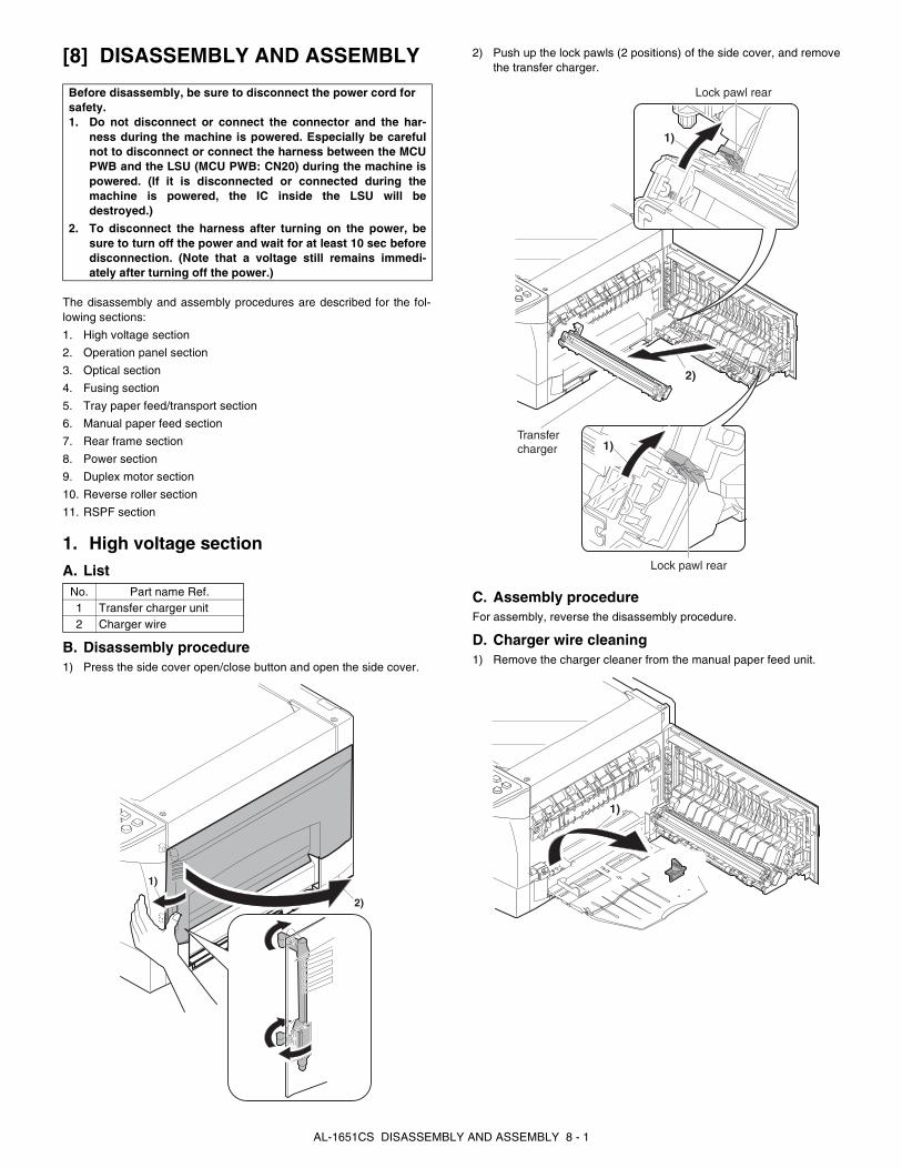
[8] DISASSEMBLY AND ASSEMBLY
The disassembly and assembly procedures are described for the fol-lowing sections:
1. High voltage section
2. Operation panel section
3. Optical section
4. Fusing section
5. Tray paper feed/transport section
6. Manual paper feed section
7. Rear frame section
8. Power section
9. Duplex motor section
10. Reverse roller section
11. RSPF section
1. High voltage sectionA. List
B. Disassembly procedure1) Press the side cover open/close button and open the side cover.
2) Push up the lock pawls (2 positions) of the side cover, and removethe transfer charger.
C. Assembly procedureFor assembly, reverse the disassembly procedure.
D. Charger wire cleaning1) Remove the charger cleaner from the manual paper feed unit.
Before disassembly, be sure to disconnect the power cord for safety.1. Do not disconnect or connect the connector and the har-
ness during the machine is powered. Especially be carefulnot to disconnect or connect the harness between the MCUPWB and the LSU (MCU PWB: CN20) during the machine ispowered. (If it is disconnected or connected during themachine is powered, the IC inside the LSU will bedestroyed.)
2. To disconnect the harness after turning on the power, besure to turn off the power and wait for at least 10 sec beforedisconnection. (Note that a voltage still remains immedi-ately after turning off the power.)
No. Part name Ref.1 Transfer charger unit2 Charger wire
1)
2)
2)
1)
1)
Lock pawl rear
Lock pawl rear
Transfercharger
1)
AL-1651CS DISASSEMBLY AND ASSEMBLY 8 - 1
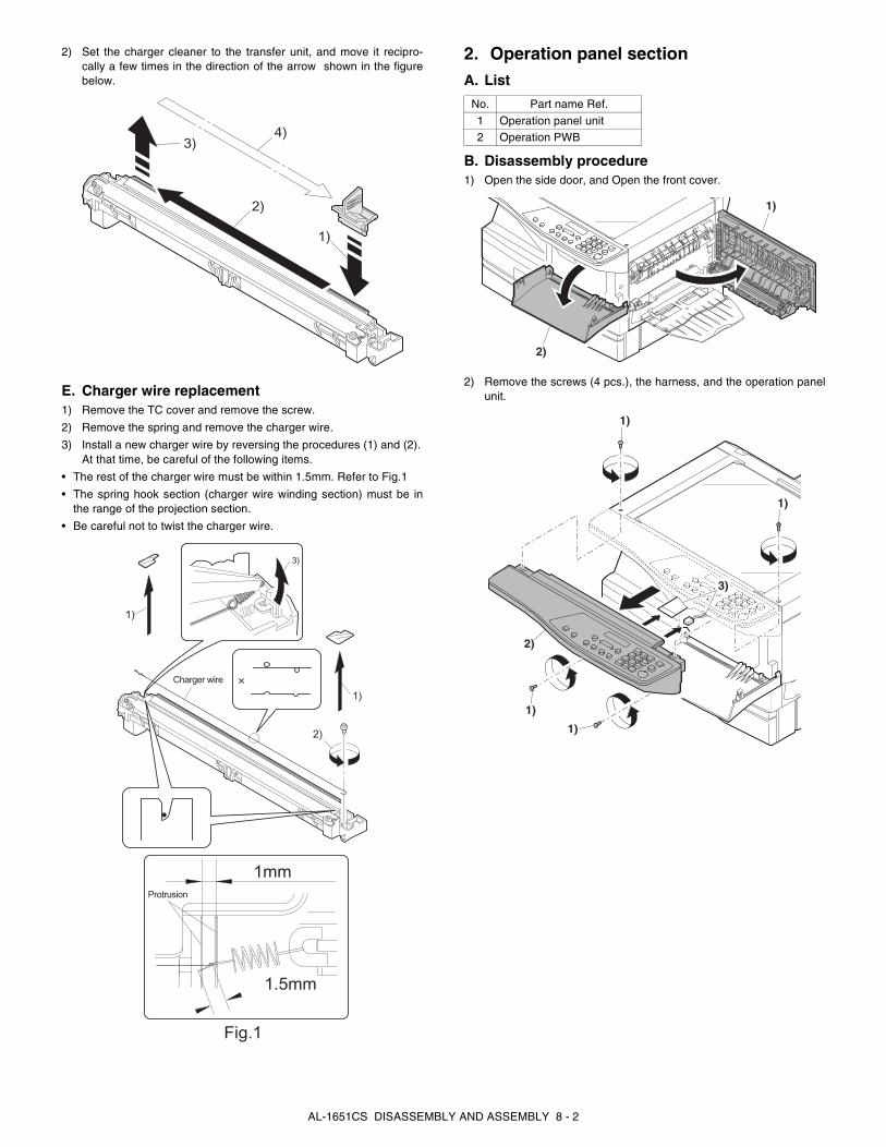
2) Set the charger cleaner to the transfer unit, and move it recipro-cally a few times in the direction of the arrow shown in the figurebelow.
E. Charger wire replacement1) Remove the TC cover and remove the screw.
2) Remove the spring and remove the charger wire.
3) Install a new charger wire by reversing the procedures (1) and (2).At that time, be careful of the following items.
• The rest of the charger wire must be within 1.5mm. Refer to Fig.1
• The spring hook section (charger wire winding section) must be inthe range of the projection section.
• Be careful not to twist the charger wire.
2. Operation panel sectionA. List
B. Disassembly procedure1) Open the side door, and Open the front cover.
2) Remove the screws (4 pcs.), the harness, and the operation panelunit.
1)
2)
3)4)
1mm
1.5mm
Fig.1
1)
1)
2)
3)
Charger wire
Protrusion
No. Part name Ref.
1 Operation panel unit2 Operation PWB
1)
2)
1)
1)
1)
1)
2)
3)
AL-1651CS DISASSEMBLY AND ASSEMBLY 8 - 2
3) Remove four screws, and remove the operation cabinet.
4) Remove four screws, and remove the operation PWB.
C. Assembly procedureFor assembly, reverse the disassembly procedure
3. Optical sectionA. List
B. Disassembly procedure1) Remove four screws, and remove the rear cabinet and the rear
cabinet cover.
2) Remove the connector and the clamp, and remove the RSPF unit.
3) Remove the four screws, remove the operation unit, and discon-nect the connector.
4) Remove the right cabinet.
5) Remove the left cabinet.
6) Remove the screw, and remove the rear cover.
7) Remove the table glass.
NO. Part name Ref.
1 Copy lamp unit
2 Copy lamp3 Lens unit
1)
1)
1)4)
1)
3)
3)
2)
Note that there are 9 pawls
1)
1)
1)1)
2)
2)
4)
1)
3)
2)
1)
1)
2)
4)
5)
6)
7)
8)
1)
1)
3)
AL-1651CS DISASSEMBLY AND ASSEMBLY 8 - 3
8) Move the carriage to the position indicated on the figure.
9) Loosen the screw which is fixing the tension plate.
10) Move the tension plate in the arrow direction to release the ten-sion, and remove the belt.
11) Remove the screw, and remove the rod stopper.
12) Remove the rod.
13) Lift the rear side of the carriage, remove the belt and the connec-tor, and remove the carriage.
C. Assembly procedure
CCD core1) Pass the core through the CCD-MCU harness.
2) Insert the CCD-MCU harness into the CCD PWB connector of thecarriage unit.
3) Move the core which was passed through the CCD-MCU harnessnear the CCD PWB connector as shown in the figure below, and fixit with a filament tape (19mm wide, 40mm long). For the attach-ment reference, refer to the figure below. Clean and remove oilfrom the attachment section.
4) Attach the CCD-MCU harness to the duplex tape on the back ofthe carriage unit.
5) Attach the PWB holder to the position specified in the figure below.
6) Pass the core through the FFC and the PWB holder, and fix thecore.1)
2) 4)
3)
1)2)
3)
1)
2)
4)
3)
Note: Attach the FCC to the base plate securely with duplex tape to prevent against coming loose.
Note: Attach the FCC to fit with the marking line. Marking line.
AL-1651CS DISASSEMBLY AND ASSEMBLY 8 - 4
4. Fusing sectionA. List
B. Disassembly procedure1) Remove the connectors (3 pcs.) of the rear cabinet.
2) Open the side cover, remove two screws, and remove the fusingunit.
3) Cut the binding band, remove the screw, and remove the ther-mistor.
4) Remove the screw and remove the U-turn guide.
Pressure roller section disassembly5) Remove the three screws, remove the fusing cover lower on the
right side, and open the heat roller section.
6) Remove the screw and remove the PPD2 sensor.
No. Part name Ref.
1 Thermistor2 PPD2 sensor
3 Heater lamp
4 Pressure roller
5 Heat roller
1)
2)
3)
2)
1)
2)
3)Thermistor
1)
2)
1)
5)
5)
6)
6)
4)3)2)
1)
2)PPD2 sensor
AL-1651CS DISASSEMBLY AND ASSEMBLY 8 - 5
7) Remove the plate spring on the right and remove the heater lamp.
8) Remove the spring and remove the separation pawls (3 pcs.).
9) Remove the E-ring and remove the reverse gate.
10) Remove the pressure release levers on the right and the left sides.
11) Remove the pressure roller, the pressure bearing, and the spring.
Note: Apply grease to the sections specified with an asterisk (*).Grease: “JFE552” UKOG-0235FCZZ
Heat roller disassembly
(Continued from procedure (4).)
5) Remove screws, remove the fusing cover, and open the heat rollersection.
1)
2)
Heater lamp
3)
1)
2)
2)
1)
3)
1)
1)
1)
2)
2)
1)
3)
3)
Pressure roller
1)
2)
2)
3)
3)
AL-1651CS DISASSEMBLY AND ASSEMBLY 8 - 6
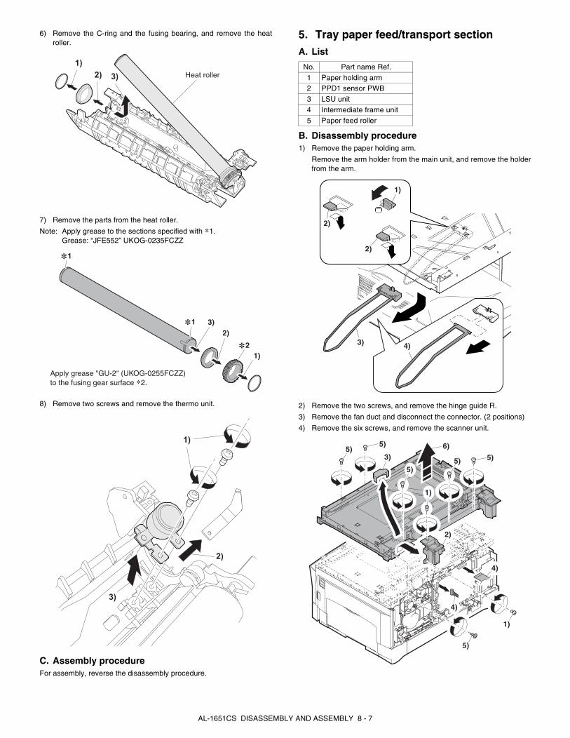
6) Remove the C-ring and the fusing bearing, and remove the heatroller.
7) Remove the parts from the heat roller.
Note: Apply grease to the sections specified with ∗1.Grease: “JFE552” UKOG-0235FCZZ
8) Remove two screws and remove the thermo unit.
C. Assembly procedureFor assembly, reverse the disassembly procedure.
5. Tray paper feed/transport sectionA. List
B. Disassembly procedure1) Remove the paper holding arm.
Remove the arm holder from the main unit, and remove the holderfrom the arm.
2) Remove the two screws, and remove the hinge guide R.
3) Remove the fan duct and disconnect the connector. (2 positions)
4) Remove the six screws, and remove the scanner unit.
1)2) 3) Heat roller
3)2)
1)
1
1
2
Apply grease "GU-2" (UKOG-0255FCZZ) to the fusing gear surface ∗2.
1)
2)
3)
No. Part name Ref.
1 Paper holding arm2 PPD1 sensor PWB
3 LSU unit
4 Intermediate frame unit
5 Paper feed roller
3)
1)
2)
2)
4)
5)5)
5) 5)
5)
4)
4)
2)
1)
1)
6)
5)
3)
AL-1651CS DISASSEMBLY AND ASSEMBLY 8 - 7

5) Disconnect the connector from the MCU PWB.
6) Disengage the pawls (2 positions), and remove the sensor PWB.
7) Remove the screw, and open the upper paper guide.
8) Remove the roller, and remove the belt.
9) Disengage the pawl, and remove the roller knob.
10) Disengage the pawl, and shift the pulley and the bearing.
11) Remove the paper exit roller, and remove the belt, the pulley, andthe bearing.
12) Disconnect the connectors.
13) Remove the three screws, and remove the MCU PWB.
1)
2)
3)
1)1)
2)
1)
2)
1)
2)3)
4)
1)2)
1)
1)
1)
2)
2)
2)
3)
AL-1651CS DISASSEMBLY AND ASSEMBLY 8 - 8
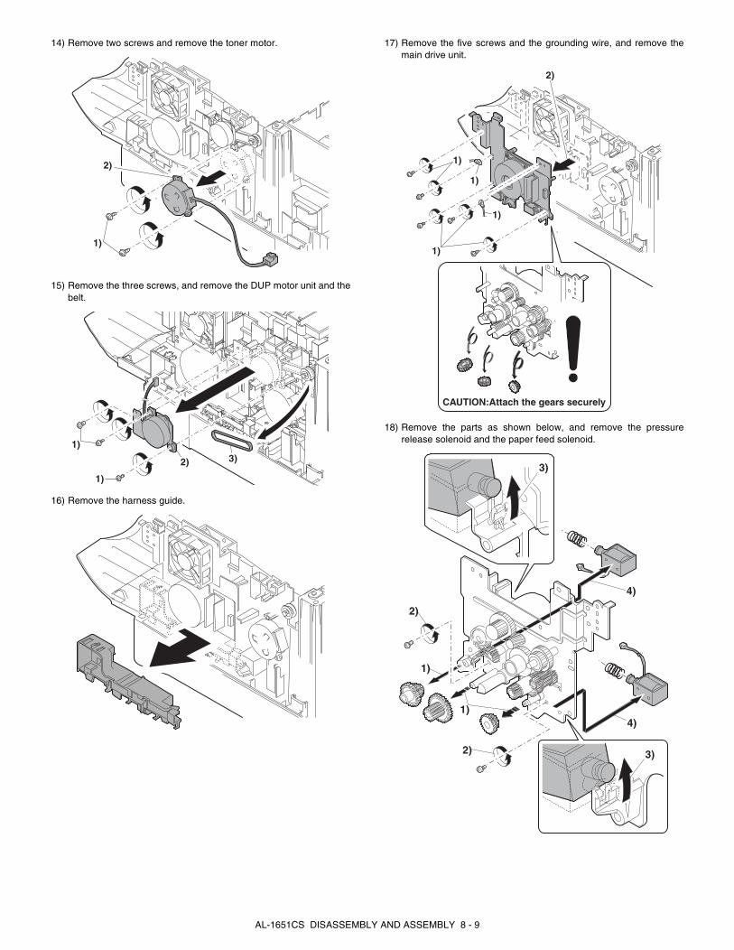
14) Remove two screws and remove the toner motor.
15) Remove the three screws, and remove the DUP motor unit and thebelt.
16) Remove the harness guide.
17) Remove the five screws and the grounding wire, and remove themain drive unit.
18) Remove the parts as shown below, and remove the pressurerelease solenoid and the paper feed solenoid.
1)
2)
1)
1)
2) 3)
1)
2)
1)
1)
1)
CAUTION:Attach the gears securely
3)
3)
1)
1)
2)
2)
4)
4)
AL-1651CS DISASSEMBLY AND ASSEMBLY 8 - 9

19) Remove each pawl, and remove the paper exit tray.
20) Remove two screws and remove the fusing connector.
21) Remove five screws and the connector, and lift the intermediateframe unit to remove.
22) Remove the four screws, and remove the lower paper guide unit.
[Note for installation]
Fit the lower paper guide hole (a) with the shifter gear hole (b) sothat the black resin (c) of the shifter unit can be checked.
23) Disengage the pawl, and remove the pulley.
24) Shift and remove the shifter unit.
25) Remove the screw, and remove the grounding plate and the gear.
26) Remove the E-ring, the gear, and the bearing, and remove theshifter roller.
2)4)
1)
3)
2)
2)
3)
3)
3)
3)
1)
4)
1)
1)1)1)
2)
abc
1)
2)
3)
3)
4)
1)
2)
3)
AL-1651CS DISASSEMBLY AND ASSEMBLY 8 - 10
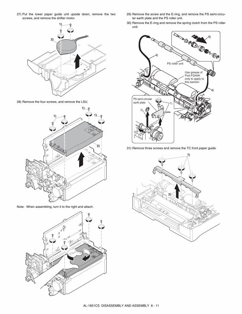
27) Put the lower paper guide unit upside down, remove the twoscrews, and remove the shifter motor.
28) Remove the four screws, and remove the LSU.
Note: When assembling, turn it to the right and attach.
29) Remove the screw and the E-ring, and remove the PS semi-circu-lar earth plate and the PS roller unit.
30) Remove the E-ring and remove the spring clutch from the PS rollerunit.
31) Remove three screws and remove the TC front paper guide.
1)
2)
1)
1)
1)
2)
5)
4)
4)
1)
2)
3)
PS roller unit
PS semi-circulerearth plate
5)
4)
4)
1)
2)
3)
PS semi-circularearth plate
Use grease of Floil FG40H only to apply to this section.
1)
2)
AL-1651CS DISASSEMBLY AND ASSEMBLY 8 - 11

32) Remove the screw and the connector, and remove the PPD1 sen-sor PWB.
33) Remove two E-rings and remove the paper feed roller.
34) Remove three E-rings and remove the clutch unit.
35) Remove the semi-circular roller unit.
36) Remove the semi-circular rubber.
C. Assembly procedureFor assembly, reverse the disassembly procedure.
6. Manual paper feed sectionA. List
B. Disassembly procedure
Multi unit1) Remove the screw and remove the multi upper cover.
1)
2)
4)
5)
1)
2)
3)
4)
Back
Front
Clutch unit
Paper feedroller
No. Part name Ref.
1 Manual transport roller
2 Cassette detection switch
3 PPD1 sensor PWB
4 Side door detection unit
2)
1)1)
2)
1)
AL-1651CS DISASSEMBLY AND ASSEMBLY 8 - 12

2) Remove the screw and remove the side door detection unit.
3) Remove three screws and remove the multi paper feed upperframe.
4) Remove two screws and remove the multi feed bracket unit fromthe multi paper feed upper frame.
5) Remove three E-rings and remove the manual paper feed rollerB9.
1)
2)
Back Wire treatment
1)
2)
1)
2)
2)
1) 1)
2)
1) 1)
1)
3)
L O C K
TO
K
AL-1651CS DISASSEMBLY AND ASSEMBLY 8 - 13
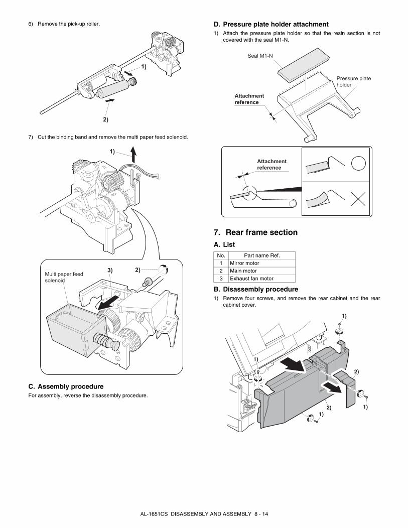
6) Remove the pick-up roller.
7) Cut the binding band and remove the multi paper feed solenoid.
C. Assembly procedureFor assembly, reverse the disassembly procedure.
D. Pressure plate holder attachment1) Attach the pressure plate holder so that the resin section is not
covered with the seal M1-N.
7. Rear frame sectionA. List
B. Disassembly procedure1) Remove four screws, and remove the rear cabinet and the rear
cabinet cover.
2)
1)
1)
2)3)Multi paper feedsolenoid
No. Part name Ref.1 Mirror motor
2 Main motor
3 Exhaust fan motor
Pressure plateholder
Seal M1-N
Attachmentreference
Attachmentreference
1)
1)
1)1)
2)
2)
AL-1651CS DISASSEMBLY AND ASSEMBLY 8 - 14
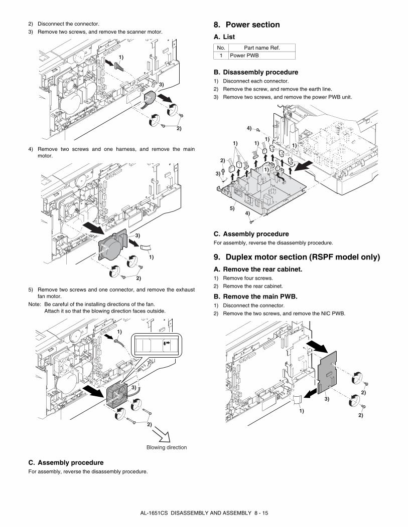
2) Disconnect the connector.
3) Remove two screws, and remove the scanner motor.
4) Remove two screws and one harness, and remove the mainmotor.
5) Remove two screws and one connector, and remove the exhaustfan motor.
Note: Be careful of the installing directions of the fan.Attach it so that the blowing direction faces outside.
C. Assembly procedureFor assembly, reverse the disassembly procedure.
8. Power sectionA. List
B. Disassembly procedure1) Disconnect each connector.
2) Remove the screw, and remove the earth line.
3) Remove two screws, and remove the power PWB unit.
C. Assembly procedureFor assembly, reverse the disassembly procedure.
9. Duplex motor section (RSPF model only)A. Remove the rear cabinet.1) Remove four screws.
2) Remove the rear cabinet.
B. Remove the main PWB.1) Disconnect the connector.
2) Remove the two screws, and remove the NIC PWB.
1)
3)
2)
1)
2)
3)
1)
2)
3)
Blowing direction
No. Part name Ref.
1 Power PWB
1) 1)1)
1)
2)
3)
4)
4)5)
1)
2)
2)
3)
1)
AL-1651CS DISASSEMBLY AND ASSEMBLY 8 - 15
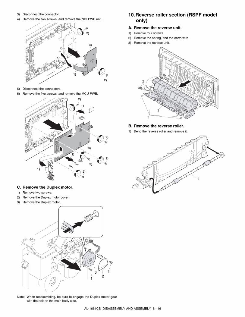
3) Disconnect the connector.
4) Remove the two screws, and remove the NIC PWB unit.
5) Disconnect the connectors.
6) Remove the five screws, and remove the MCU PWB.
C. Remove the Duplex motor.1) Remove two screws.
2) Remove the Duplex motor cover.
3) Remove the Duplex motor.
Note: When reassembling, be sure to engage the Duplex motor gearwith the belt on the main body side.
10.Reverse roller section (RSPF model only)
A. Remove the reverse unit.1) Remove four screws
2) Remove the spring, and the earth wire
3) Remove the reverse unit.
B. Remove the reverse roller.1) Bend the reverse roller and remove it.
2)
2)
3)
3)
1)
1)
1)
1)
2)
2)
3)
2)
2)
2)
12
3
1
1
2
3
1
AL-1651CS DISASSEMBLY AND ASSEMBLY 8 - 16
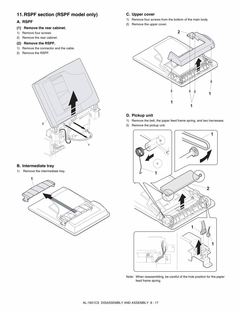
11.RSPF section (RSPF model only)A. RSPF
(1) Remove the rear cabinet.1) Remove four screws.
2) Remove the rear cabinet.
(2) Remove the RSPF.1) Remove the connector and the cable.
2) Remove the RSPF.
B. Intermediate tray1) Remove the intermediate tray.
C. Upper cover1) Remove four screws from the bottom of the main body.
2) Remove the upper cover.
D. Pickup unit1) Remove the belt, the paper feed frame spring, and two harnesses.
2) Remove the pickup unit.
Note: When reassembling, be careful of the hole position for the paperfeed frame spring.
1
2
1
1
2
1
1
1
1
2
1
1
AL-1651CS DISASSEMBLY AND ASSEMBLY 8 - 17

E. Upper cover of the pickup unit.1) Remove two screws from the bottom of the pickup unit.
2) Remove the upper cover.
F. Sensor PWB1) Remove two screws.
2) Remove the sensor PWB.
3) Remove the harness.
G. Pickup solenoid1) Remove two screws.
2) Remove the pickup solenoid.
Note: When reassembling, hang the iron core on the solenoid arm.
H. Clutch
(1) Remove the clutch unit.1) Remove the E-ring.
2) Remove the pulley and the bush.
3) Slide the bush in the arrow direction.
4) Lift the clutch pawl.
5) Remove the clutch unit.
1
2
1
11
2
3
12
A
1
5
2
43
AL-1651CS DISASSEMBLY AND ASSEMBLY 8 - 18
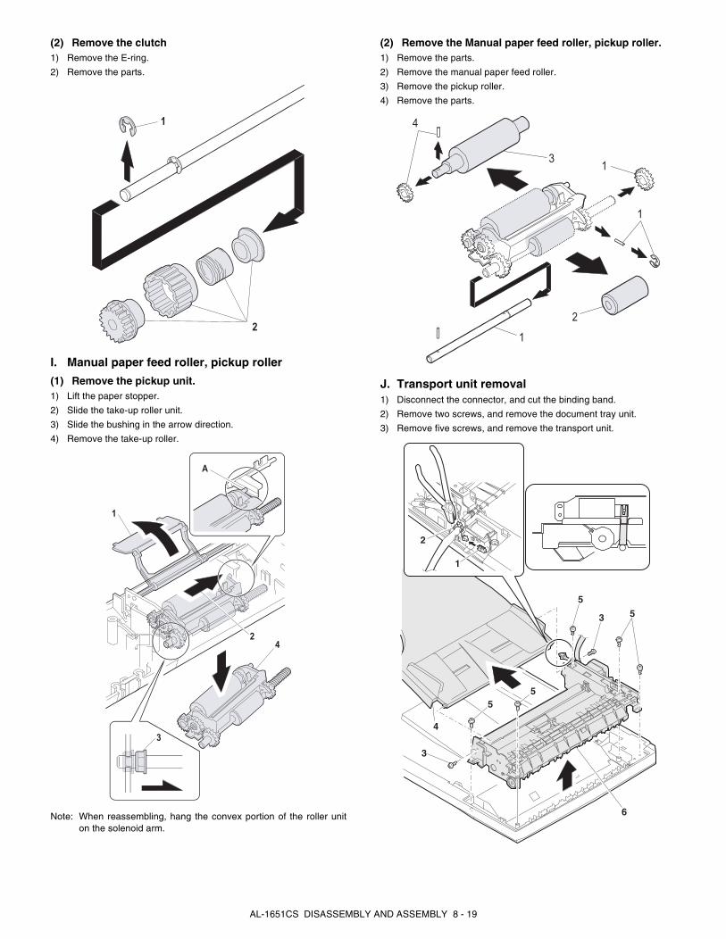
(2) Remove the clutch1) Remove the E-ring.
2) Remove the parts.
I. Manual paper feed roller, pickup roller
(1) Remove the pickup unit.1) Lift the paper stopper.
2) Slide the take-up roller unit.
3) Slide the bushing in the arrow direction.
4) Remove the take-up roller.
Note: When reassembling, hang the convex portion of the roller uniton the solenoid arm.
(2) Remove the Manual paper feed roller, pickup roller.1) Remove the parts.
2) Remove the manual paper feed roller.
3) Remove the pickup roller.
4) Remove the parts.
J. Transport unit removal1) Disconnect the connector, and cut the binding band.
2) Remove two screws, and remove the document tray unit.
3) Remove five screws, and remove the transport unit.
1
2
1
42
3
A
1
2
31
1
4
3
4
5
1
3
5
55
6
2
AL-1651CS DISASSEMBLY AND ASSEMBLY 8 - 19
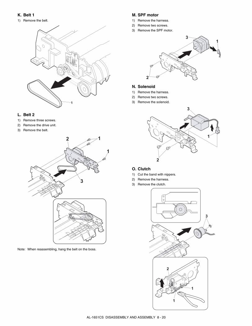
K. Belt 11) Remove the belt.
L. Belt 21) Remove three screws.
2) Remove the drive unit.
3) Remove the belt.
Note: When reassembling, hang the belt on the boss.
M. SPF motor1) Remove the harness.
2) Remove two screws.
3) Remove the SPF motor.
N. Solenoid1) Remove the harness.
2) Remove two screws.
3) Remove the solenoid.
O. Clutch1) Cut the band with nippers.
2) Remove the harness.
3) Remove the clutch.
1
12
3
1
1
2
3
1
2
3
1
1
2
3
AL-1651CS DISASSEMBLY AND ASSEMBLY 8 - 20

P. Paper supply roller
(1) Remove the parts.1) Remove the two screws.
2) Remove the parts.
(2) Remove the paper supply roller.1) Loosen the screw.
2) Open the paper exit paper guide.
3) Remove the parts.
4) Remove the paper supply roller.
Q. Paper entry sensor1) Loosen the screw.
2) Open the paper exit paper guide.
3) Remove the paper entry sensor.
4) Remove the harness.
R. Transport roller 1.
(1) Remove the parts.1) Remove the parts.
1
21
2 1
3
3
4
1
4
2
3
1
1
1
AL-1651CS DISASSEMBLY AND ASSEMBLY 8 - 21

(2) Remove the parts.1) Loosen the screw.
2) Open the paper exit paper guide.
3) Remove the parts.
(3) Remove the transport roller.1) Remove the paper exit paper guide.
2) Remove the transport roller.
S. Paper exit roller
(1) Remove the parts.1) Remove two screws.
2) Remove the parts.
(2) Remove the paper feed paper guide upper.1) Remove two screws.
2) Remove the paper feed paper guide upper.
12
3
1
2
1
1
2
1
2
AL-1651CS DISASSEMBLY AND ASSEMBLY 8 - 22

(3) Remove the paper exit roller.1) Remove the parts.
2) Remove the paper exit roller.
T. Solenoid
(1) Remove the reverse gate1) Remove the ring
2) Remove the reverse gate
Note: When reassembling, be careful of the groove and the holepositions of the spring.
Note: When reassembling, hang 2) on the solenoid.
(2) Remove the solenoid.1) Remove the screw.
2) Remove the solenoid.
1
1
2
1
2
1
2
AL-1651CS DISASSEMBLY AND ASSEMBLY 8 - 23
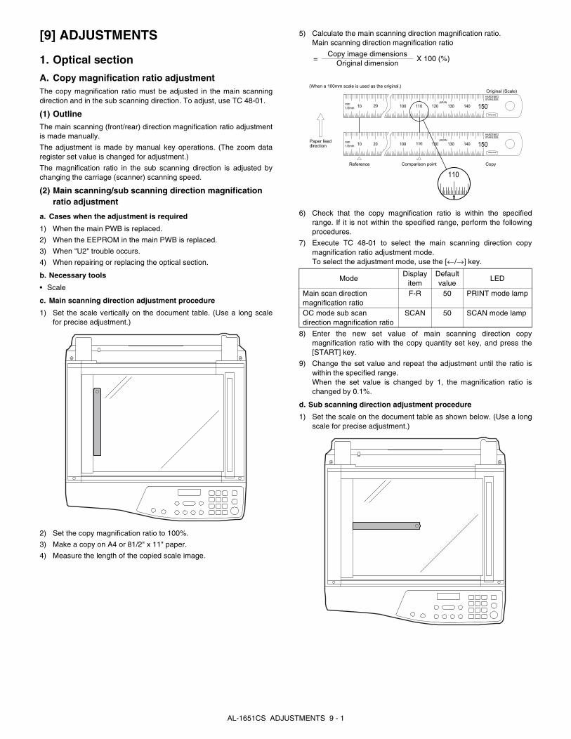
[9] ADJUSTMENTS
1. Optical section
A. Copy magnification ratio adjustmentThe copy magnification ratio must be adjusted in the main scanningdirection and in the sub scanning direction. To adjust, use TC 48-01.
(1) OutlineThe main scanning (front/rear) direction magnification ratio adjustmentis made manually.
The adjustment is made by manual key operations. (The zoom dataregister set value is changed for adjustment.)
The magnification ratio in the sub scanning direction is adjusted bychanging the carriage (scanner) scanning speed.
(2) Main scanning/sub scanning direction magnification ratio adjustment
a. Cases when the adjustment is required
1) When the main PWB is replaced.
2) When the EEPROM in the main PWB is replaced.
3) When "U2" trouble occurs.
4) When repairing or replacing the optical section.
b. Necessary tools
• Scale
c. Main scanning direction adjustment procedure
1) Set the scale vertically on the document table. (Use a long scalefor precise adjustment.)
2) Set the copy magnification ratio to 100%.
3) Make a copy on A4 or 81/2" x 11" paper.
4) Measure the length of the copied scale image.
5) Calculate the main scanning direction magnification ratio. Main scanning direction magnification ratio
6) Check that the copy magnification ratio is within the specifiedrange. If it is not within the specified range, perform the followingprocedures.
7) Execute TC 48-01 to select the main scanning direction copymagnification ratio adjustment mode.To select the adjustment mode, use the [←/→] key.
8) Enter the new set value of main scanning direction copymagnification ratio with the copy quantity set key, and press the[START] key.
9) Change the set value and repeat the adjustment until the ratio iswithin the specified range.When the set value is changed by 1, the magnification ratio ischanged by 0.1%.
d. Sub scanning direction adjustment procedure
1) Set the scale on the document table as shown below. (Use a longscale for precise adjustment.)
=Copy image dimensions
X 100 (%)Original dimension
ModeDisplay
itemDefault value
LED
Main scan direction magnification ratio
F-R 50 PRINT mode lamp
OC mode sub scan direction magnification ratio
SCAN 50 SCAN mode lamp
100 110 120 130 150140mm1/2mm
JAPAN
HARDENEDSTAINLESS
Shizuoka
100 110 120 130 150140mm1/2mm
JAPAN
HARDENEDSTAINLESS
Shizuoka
110
10 20
10 20
(When a 100mm scale is used as the original.)
Paper feeddirection
Reference Comparison point
Original (Scale)
Copy
AL-1651CS ADJUSTMENTS 9 - 1
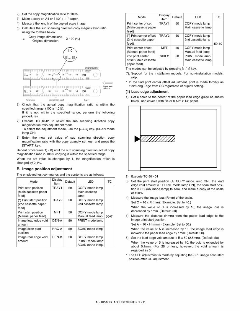
2) Set the copy magnification ratio to 100%.
3) Make a copy on A4 or 81/2" x 11" paper.
4) Measure the length of the copied scale image.
5) Calculate the sub scanning direction copy magnification ratiousing the formula below.
6) Check that the actual copy magnification ratio is within thespecified range. (100 ± 1.0%).If it is not within the specified range, perform the followingprocedures.
7) Execute TC 48-01 to select the sub scanning direction copymagnification ratio adjustment mode.To select the adjustment mode, use the [←/→] key. (SCAN modelamp ON)
8) Enter the new set value of sub scanning direction copymagnification ratio with the copy quantity set key, and press the[START] key.
Repeat procedures 1) - 8) until the sub scanning direction actual copymagnification ratio in 100% copying is within the specified range.
When the set value is changed by 1, the magnification ration ischanged by 0.1%.
B. Image position adjustmentThe employed test commands and the contents are as follows:
The modes can be selected by pressing [←/→] key.
(*): Support for the installation models. For non-installation models,skip.
* In the 2nd print center offset adjustment, print is made forcibly as1to2/Long Edge from OC regardless of duplex setting.
(1) Lead edge adjustment1) Set a scale to the center of the paper lead edge guide as shown
below, and cover it with B4 or 8 1/2" x 14" paper.
2) Execute TC 50 - 01
3) Set the print start position (A: COPY mode lamp ON), the leadedge void amount (B: PRINT mode lamp ON), the scan start posi-tion (C: SCAN mode lamp) to zero, and make a copy of the scaleat 100%.
4) Measure the image loss (Rmm) of the scale.
Set C = 10 x R (mm). (Example: Set to 40.)
When the value of C is increased by 10, the image loss isdecreased by 1mm. (Default: 50)
5) Measure the distance (Hmm) from the paper lead edge to theimage print start position.
Set A = 10 x H (mm). (Example: Set to 50.)
When the value of A is increased by 10, the image lead edge ismoved to the paper lead edge by 1mm. (Default: 50).
6) Set the lead edge void amount to B = 50 (2.5mm). (Default: 50)
When the value of B is increased by 10, the void is extended byabout 0.1mm. (For 25 or less, however, the void amount isregarded as 0.)
* The SFP adjustment is made by adjusting the SPF image scan startposition after OC adjustment.
=Copy image dimensions
X 100 (%)Original dimension
ModeDisplay
itemDefault LED TC
Print start position (Main cassette paper feed)
TRAY1 50 COPY mode lampMain cassette lamp
50-01
(*) Print start position (2nd cassette paper feed)
TRAY2 50 COPY mode lamp2nd cassette lamp
Print start position (Manual paper feed)
MFT 50 COPY mode lampManual feed lamp
Image lead edge void amount
DEN-A 50 PRINT mode lamp
Image scan start position
RRC-A 50 SCAN mode lamp
Image rear edge void amount
DEN-B 50 COPY mode lampPRINT mode lampSCAN mode lamp
100 110 120 130 150140mm1/2mm
JAPAN
HARDDENCDSTAINLESS
Shizuoka
100 110 120 130 150140mm1/2mm
JAPAN
HARDDENCDSTAINLESS
Shizuoka
110
10 20
10 20
Original (Scale)
Paper feeddirection
Reference Comparison point Copy
ModeDisplay
itemDefault LED TC
Print center offset (Main cassette paper feed)
TRAY1 50 COPY mode lampMain cassette lamp
50-10
(*) Print center offset (2nd cassette paper feed)
TRAY2 50 COPY mode lamp2nd cassette lamp
Print center offset (Manual paper feed)
MFT 50 COPY mode lampManual feed lamp
2nd print center offset (Main cassette paper feed)
SIDE2 50 PRINT mode lampMain cassette lamp
AL-1651CS ADJUSTMENTS 9 - 2
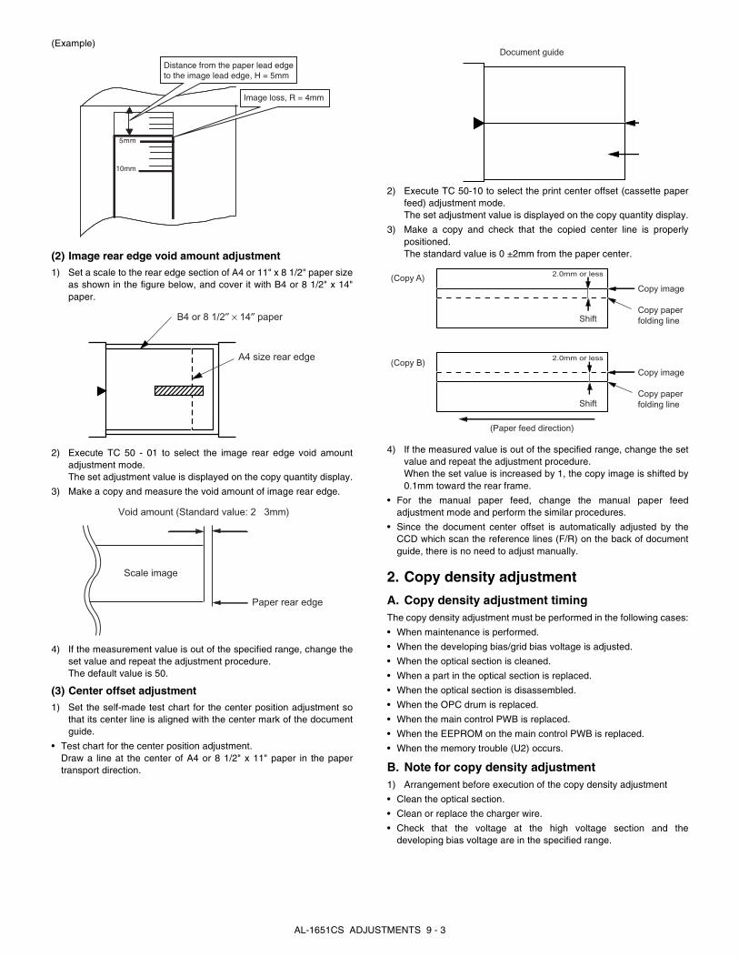
(Example)
(2) Image rear edge void amount adjustment1) Set a scale to the rear edge section of A4 or 11" x 8 1/2" paper size
as shown in the figure below, and cover it with B4 or 8 1/2" x 14"paper.
2) Execute TC 50 - 01 to select the image rear edge void amountadjustment mode.The set adjustment value is displayed on the copy quantity display.
3) Make a copy and measure the void amount of image rear edge.
4) If the measurement value is out of the specified range, change theset value and repeat the adjustment procedure.The default value is 50.
(3) Center offset adjustment1) Set the self-made test chart for the center position adjustment so
that its center line is aligned with the center mark of the documentguide.
• Test chart for the center position adjustment.Draw a line at the center of A4 or 8 1/2" x 11" paper in the papertransport direction.
2) Execute TC 50-10 to select the print center offset (cassette paperfeed) adjustment mode.The set adjustment value is displayed on the copy quantity display.
3) Make a copy and check that the copied center line is properlypositioned.The standard value is 0 ±2mm from the paper center.
4) If the measured value is out of the specified range, change the setvalue and repeat the adjustment procedure.When the set value is increased by 1, the copy image is shifted by0.1mm toward the rear frame.
• For the manual paper feed, change the manual paper feedadjustment mode and perform the similar procedures.
• Since the document center offset is automatically adjusted by theCCD which scan the reference lines (F/R) on the back of documentguide, there is no need to adjust manually.
2. Copy density adjustment
A. Copy density adjustment timingThe copy density adjustment must be performed in the following cases:
• When maintenance is performed.
• When the developing bias/grid bias voltage is adjusted.
• When the optical section is cleaned.
• When a part in the optical section is replaced.
• When the optical section is disassembled.
• When the OPC drum is replaced.
• When the main control PWB is replaced.
• When the EEPROM on the main control PWB is replaced.
• When the memory trouble (U2) occurs.
B. Note for copy density adjustment1) Arrangement before execution of the copy density adjustment
• Clean the optical section.
• Clean or replace the charger wire.
• Check that the voltage at the high voltage section and thedeveloping bias voltage are in the specified range.
5mm
10mm
Distance from the paper lead edge to the image lead edge, H = 5mm
Image loss, R = 4mm
B4 or 8 1/2″ × 14″ paper
A4 size rear edge
Scale image
Paper rear edge
Void amount (Standard value: 2 3mm)
Document guide
(Copy A)
(Copy B)
2.0mm or less
2.0mm or less
Copy image
Copy paperfolding line
Copy image
Copy paperfolding line
Shift
Shift
(Paper feed direction)
AL-1651CS ADJUSTMENTS 9 - 3

C. Necessary tool for copy density adjustment• One of the following test charts:
UKOG-0162FCZZ, UKOG-0089CSZZ, KODAK GRAY SCALE
• B4 (14" x 8 1/2") white paper
• The user program AE setting should be "3."
Test chart comparison table
D. Features of copy density adjustmentFor the copy density adjustment, the image data shift function providedin the image process LSI is used.
List of the adjustment modes
E. Copy density adjustment procedureThe copy density can be adjusted in 300dpi or in 600dpi.
For selection of modes, use the copy mode select key.
(1) Test chart (UKOG-0162FCZZ) setting1) Place the test chart so that its edge is aligned with the A4 (Letter)
reference line on the document table. Then place a A4 (14" x 8 1/2") white paper on the test chart and close the document cover.
(2) Perform the adjustment in each mode.1) Execute TC 46-01 (300dpi). To adjust in 600dpi, execute TC 46-
02.
2) Select the mode to be adjusted with the exposure mode select key.Set the exposure level to 3 (center) for all adjustment. (Except forthe auto mode.)
3) Make a copy.Check the adjustment level (shown in the above table) of theexposure test chart (Sharp Gray Scale).
(When too bright): Decrease the value displayed on the copy quantitydisplay.
(When too dark): Increase the value displayed on the copy quantitydisplay.
* The value can be set in the range of 1 - 99.
UKOG-0162FCZZ DENSITY No.
1 2 3 4 5 6 7 8 9 10 W
UKOG-0089CSZZ DENSITY No.
0.1 0.2 0.3 0.5 1.9 0
KODAK GRAY SCALE
1 2 3 4 19 A
Auto Mode Brightness 1 step onlyManual Mode Brightness 5 steps. Adjustment of only the center
brightness is made.Photo Mode Brightness 5 steps. Adjustment of only the center
brightness is made.Manual T/S mode
Brightness 5 steps. Adjustment of only the center brightness is made.
T/S Auto mode Brightness 1 step only
Main code Sub code Resolution for copy density adjustment
4601 300dpi02 600dpi
1 10 W2 3 4 5 6 7 8 9
White paper
Test chartTest chart
Adjustment mode
Display item
LEDSharp gray chart adjustment level
Auto mode AE COPY mode lamp "3" is slightly copied.
Text mode TEXT PRINT mode lamp "3" is slightly copied.
Photo mode PHOTO SCAN mode lamp "3" is slightly copied.
Text T/S mode TSTXT PRINT mode lampSCAN mode lamp
"3" is slightly copied.
Auto T/S mode TSAE COPY mode lampSCAN mode lamp
"3" is slightly copied.
Sharp Gray Scale adjustment level
Non toner save mode
Toner save mode
(2) Mode select key
TEXT | | | | | (1) Exposure mode, level display
1 10 W2 3 4 5 6 7 8 9
Slightly copied.
Not copied.
1 10 W2 3 4 5 6 7 8 9
Slightly copied.
Not copied.
AL-1651CS ADJUSTMENTS 9 - 4

3. High voltage adjustment
A. Main charger (Grid bias)Note:
• Use a digital multi meter with internal resistance of 10MΩ or moremeasurement.
• After adjusting the grid LOW output, adjust the HIGH output. Do notreverse the sequence.
Procedures
1) Set the digital multi meter range to DC700V.
2) Set the positive side of the test rod to the connector CN11-3(GRID) of high voltage section of the power PWB and set thenegative side to the frame ground (power frame).
3) Execute TC 8-02. (The main charger output is supplied for 30 secin the grid voltage HIGH output mode.)
4) Adjust the control volume (VRG1) so that the output voltage is 580±12V.
B. DV bias check
Procedures
1) Set the digital multi meter range to DC500V.
2) Set the positive side of the test rod to the connector CN-10-1 (DVBIAS) and set the negative side to the frame ground (powerframe).
3) Execute TC 25-01 to output the developing bias for 30sec, andcheck that the output is –400±8V.
4. Duplex adjustment
A. Adjusting the paper reverse position in memory for duplex copying
This step adjusts the front surface printing (odd-number pages of adocument set) in the S-D mode copying and the leading edge positionof an image on even-number pages in the D-S mode.
That is, it covers the adjustment of the second surface printing mode(image loss at the front edge of an image) in which image data is oncestored in memory.
The image data is read, starting from its front end in the documentdelivery direction (Reference direction of document setting in the OCmode)and stored in memory.
This stored image data is printed starting at the printing start position,in the order of last-stored data to the first-stored data.
In other words, the front edge image loss of the image can be adjustedby changing the document read end position.
(Adjustment procedure)
1) Preparing test chart (Draw a scale at the rear end of one side of asheet of A4 white paper or letter paper)
2) Set the test chart so that the scale is positioned as shown below, inthe S-D mode and the D-S mode.
3) Execute test command 50-18.
Select the SPF memory reverse output position, and press[START] key to make a copy.
Adjust the setting so that the front edge image loss is less than 4.0mm in the R-SPF mode.An increase of 1 in setting represents an increase of 0.1 mm inimage loss.
Note: • A digital multi meter with internal resistance of 1GΩ must beuse for correct check.
• The adjustment volume is locked, and no adjustment can bemade.
VRG1
VRDV
ModeDisplay
itemDefault LED
OC memory reverse output position
OC 50 COPY mode lamp
SPF memory reverse output position
SPF 50 PRINT mode lamp
5 10
Scale (S-D mode) Scale (D-S mode)
5 10
The front edge of thescale on test chart
Front edge of paper
Void area
less than 4 mm
AL-1651CS ADJUSTMENTS 9 - 5

B. Adjusting trailing edge void in duplex copy modeThis is the adjustment of the first surface printing mode (rear end void)in duplex copying.
In a duplex copying operation, the paper is delivered starting from therear end of the first printing surface. It is therefore necessary to make avoid area at the rear end on the first printing surface to prevent paperjam at the fusing part.
There are two adjustment modes:
1) Image cut rear end void quantity (R-SPF) 50-19 (SCAN modelamp)The size (length) of a document read from the R-SPF is detected,the image at the trailing edge of the first printing surface is cut tomake a void area. (The adjustment of void quantity at the timewhen the cassette paper size is not recognized.)
2) Paper trailing edge void quantity 50-19 (PRINT mode lamp)This adjustment is made when the cassette paper size isrecognized. The trailing edge void quantity can be adjusted bychanging the trailing edge image laser OFF timing.
The paper void quantity should be first adjusted before the image cuttrailing edge void quantity (R-SPF) is adjusted.
The adjustment modes can be selected by pressing [←/→] key.(Adjustment range; 1 – 99)
Enter the adjustment value and press [START] key to save the setvalue and make a copy. (The paper information is cleared for everycopy.)
When the set value is increased by 1, the void amount is increased byabout 0.1mm.
* The initial value of duplex setting is 2to2.
(Adjustment procedure)
(1) Paper trailing edge void quantity1) Preparing test chart (Draw a scale at the rear end of one side of a
sheet of A/4 white paper or letter paper)
2) Set the test chart on the document glass as shown below.
3) Execute test command 50-19 to turn on the PRINT mode lamp andmake the printing mode in OC-D mode.Make a copy of the test chart to check the void area of the scale onthe image.
Adjust the setting so that the void area is 4 - 5 mm. An increase in 1 ofsetting represents 0.1 mm in void area.
(2) Image cut trailing edge void quantity (R-SPF)1) Set the test chart so that the scale is positioned as shown below.
2) Execute test command 50-19 to turn on the SCAN mode lamp(onthe operation panel) and make the printing mode in the D-D mode.
3) Remove and reinsert the cassette.
Note: Make sure to carry out this step before making a copy duringthis adjustment.
4) Make a copy and check the void area of the scale on the image.Adjust the setting so that the void area is 2 - 4 mm. An increase of1 in setting represents an increase of 0.1 mm in void area.l Void position to be checked
ModeDisplay
itemDefault LED
Paper rear edge void amount
DEN-B 50 PRINT mode lamp
Print start position (Duplex back surface)
RRC-D 50 SCAN mode lamp
2nd printing surface where scale is printed (lower side)
Document guide The trailing edge has a scale
Table glass
The trailing edge void on the first printing surface is shown above.
Paper
Void position to be check
Scale (D-D mode)
AL-1651CS ADJUSTMENTS 9 - 6

5. SPF (RSPF) scan position automatic adjustment
Place a black chart so that it covers the SPF scan glass and the OCglass together, and close the OC cover.
When test command 53-08 is executed, the current adjustment valueis displayed as the initial display.
* Default is 1. Adjustment range is 1 – 99. Adjustment unit 1 = about0.127mm
* If the values are kept as the default values, SPF scan is not per-formed properly. The front area of the proper scan position may bescanned.
In case of AUTO, press [START] key, and the mirror unit scans fromthe home position to the SPF scan position with the adjustment valuedisplayed. The SPF glass cover edge position is calculated from thedifference between the SPFG glass cover edge and the OC sidedocument glass CCD output level. If the adjustment is normal, theadjusted value is displayed. If abnormal, the error LED lights up withthe current set value displayed.
During the error LED is lighted, when [START] key is pressed again,execution is performed again.
Operation
The operation is similar to test command 46-01. (In MANUAL)
OK/ERR display in AUTO
* Use a black chart (UKOG-0011QSZZ) or prepare a chart as shownbelow.Chart size: 300 x 100, prepared with cutting sheet No. 791 (Black) oran equivalent one.
6. RSPF (SPF) mode sub scanning direction magnification ratio adjustment
Note: Before performing this adjustment, be sure to check that the OCmode adjustment in copying has been completed.
1) Put a scale on the original table as shown below, and make anormal copy (100%) on the front and the back surfaces to make atest chart.
Note: Since the printed copy is used as a test chart, put the scale inparalled with the edge lines.
2) Set the test chart on the RSPF and make a duplex copy (D-D or D-S) in the normal ratio (100%).
3) Compare the scale image and the actual image.If necessary, perform the following adjustment procedures.
4) Execute TC 48-05.
5) The current front surface sub scanning direction magnification ratiocorrection value is displayed in two digits on the display section.To select SIDE1 and SIDE2, use [←/→] keys.
6) Enter the set value and press the start key.
When adjusting the RSPF, use [2-SIDED COPY] key to selectsingle/duplex after entering the one page print mode, performing 2-page single copy.
* When there is no document in SPF, copy is inhibited.
<Adjustment specification>
ModeDisplay
itemDefault LED
SPF scan position auto adjustment
AUTO 1 COPY mode lamp
SPF scan position manual adjustment
MANU 1 PRINT mode lamp
Reason: To prevent erroneous detection by disturbing light of afluorescent lamp, etc.
<When OK> <When ERR>
53-08 SPF AUTOAUTO 100% ** OK
53-08 SPF AUTOAUTO 100% ** ERR
6cm or more is required.
The size of the black chart (UKOG-0011QSZZ) is 297 x 420. Divide itinto four for use.
ModeDisplay
itemDefault LED
Sub scan magnification ratio adjustment on the surface of SPF/RSPF document
SIDE1 50 COPY mode lamp
Sub scan magnification ratio adjustment on the surface of RSPF document
SIDE2 50 PRINT mode lamp
Adjustment mode
Spec value TC Set valueSetting range
Sub scanning direction magnification ratio (SPF/RSPF mode)
At normal: ±1.0%
48-5 Add 1: 0.1% increaseReduce 1: 0.1% decrease
1 – 99
AL-1651CS ADJUSTMENTS 9 - 7
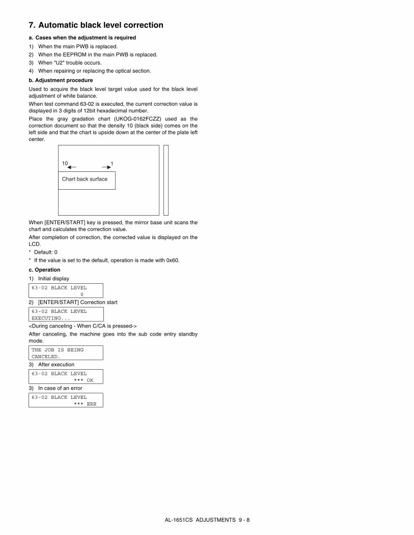
7. Automatic black level correctiona. Cases when the adjustment is required
1) When the main PWB is replaced.
2) When the EEPROM in the main PWB is replaced.
3) When "U2" trouble occurs.
4) When repairing or replacing the optical section.
b. Adjustment procedure
Used to acquire the black level target value used for the black leveladjustment of white balance.
When test command 63-02 is executed, the current correction value isdisplayed in 3 digits of 12bit hexadecimal number.
Place the gray gradation chart (UKOG-0162FCZZ) used as thecorrection document so that the density 10 (black side) comes on theleft side and that the chart is upside down at the center of the plate leftcenter.
When [ENTER/START] key is pressed, the mirror base unit scans thechart and calculates the correction value.
After completion of correction, the corrected value is displayed on theLCD.
* Default: 0
* If the value is set to the default, operation is made with 0x60.
c. Operation
1) Initial display
2) [ENTER/START] Correction start
<During canceling - When C/CA is pressed->
After canceling, the machine goes into the sub code entry standbymode.
3) After execution
3) In case of an error
63-02 BLACK LEVEL 0
63-02 BLACK LEVELEXECUTING...
THE JOB IS BEINGCANCELED.
63-02 BLACK LEVEL *** OK
63-02 BLACK LEVEL *** ERR
Chart back surface
10
AL-1651CS ADJUSTMENTS 9 - 8

[10] TEST COMMAND, TROUBLE CODES
1. Entering the test command modeTo enter the serviceman test command mode, press the keys asfollows:[#] key → [*] key → [C] key → [*] key
To cancel the test command mode, press the [CA] key.
2. Key rule
3. List of test commands
[10KEY]: Entry of MAIN CODE/SUB CODESelection of an itemSetup of an adjustment value in case of test commands for adjustment
[←/→]: Selection of MAIN CODE/SUB CODE Selection of an item
[ENTER/START]: Settlement<In case of test commands for print>[ENTER]: Settlement (Without print)[START]: Settlement/Print
[C]: (Interrupting operation check) Returns to the upper hierarchy.[ENTER] After pressing: Settles the item and returns to the upper hierarchy. [ENTER] Before pressing: Without settling the item, returns to the upper hierarchy.
In case of test command of operation check, terminates the operations. [CA]: Exits from the test command mode.
For a test command of adjustment, the display returns to the initial display (00-00).
Main code
Sub code
Contents
1 01 Mirror scan (SCAN CHK)02 Mirror home position sensor (MHPS) status display
(MHP-SENSOR)06 Mirror scan aging (SCAN AGING)
2 01 Single Paper Feeder (SPF) aging (SPF AGING)02 SPF sensor status display (SPF SENSOR)03 SPF motor operation check (SPF MOTOR CHK)06 RSPF resist clutch operation check (RSPF RES.CHK)08 SPF paper feed solenoid operation check (SPF SPUS
CHK)09 RSPF reverse solenoid operation check (RSPF SPFS
CHK)10 RSPF paper exit gate solenoid operation check
(RSPF SGS CHK)3 03 Shifter operation check (SHIFTER CHK)5 01 Operation panel display check (LCD/LED CHK)
02 Fusing lamp, cooling fan operation check (HT LAMP CHK)
03 Copy lamp ON check (C-LAMP CHK)
6 01 Paper feed solenoid (CPFS1, CPFS2, MPFS) operation check (PSOL CHK)
02 Resist roller solenoid (RRS) operation check (RES.R SOL CHK)
7 01 Check of warm-up display and aging with JAM (W-UP/AGING)
06 Interval aging (INTERVAL AGING)08 Shift to copy with warm-up display (Shift to equivalent
to CA key) (W-UP C-MODE)8 01 Developing bias output (DVLP BIAS SET.)
02 Main charger output (Grid HIGH) (MHV(H) SET.)03 Main charger output (Grid LOW) (MHV(L) SET.)06 Transfer charger output (THV SET.)
9 01 Duplex motor normal rotation check (DPLX ROT.)02 Duplex motor reverse rotation check (DPLX
ROT.REV.)10 00 Toner motor operation (TONER MOTOR)14 00 Cancel of trouble other than U2 (TRBL CANC.)16 00 U2 trouble cancel (U2 TRBL CANC.)22 04 JAM total counter display (JAM TTL CNT)
05 Total counter display (TTL CNT)08 SPF counter display (SPF CNT)12 Drum counter display (DRUM CNT)14 ROM version display (ROM VER.)16 Duplex counter display (DPLX CNT)17 Copy counter display (COPIES CNT)18 Printer counter display (PRT.CNT)19 Scanner mode counter display (S-MODE CNT)21 Scanner counter display (SCAN CNT)22 SPF JAM counter display (S JAM CNT)
24 01 JAM total counter clear (JAM TTL CLR.)04 SPF counter clear (SPF CLR.)05 Duplex counter clear (DPLX CLR.)07 Drum counter clear (DRUM CLR.)08 Copy counter clear (COPIES CLR.)09 Printer counter clear (PRT.CLR.)13 Scanner counter clear (SCAN CLR.)14 SPF JAM total counter clear (S JAM TTL CLR.)15 Scanner mode counter clear (S-MODE CLR.)
25 01 Main motor operation check (MAIN MOTOR CHK)10 Polygon motor operation check (LSU CHK)
Main code
Sub code
Contents
AL-1651CS TEST COMMAND, TROUBLE CODES 10 - 1
4. Descriptions of various test commands
26 01 Manual feed setting (BYPASS)02 (R)SPF setting (SPF/RSPF)03 Second cassette setting (2ND TRAY)04 Main unit duplex setting (DPLX)06 Destination setting (DESTINATION)07 Machine conditions check (CPM)20 Rear edge void setting (END EDGE)30 CE mark support control ON/OFF (CE MARK)38 Cancel of stop at drum life over (DRUM LIFE END)39 Memory capacity check (MEM.CHK)40 Polygon motor OFF time setting (Time required from
completion of printing to turning OFF the motor) (LSU MOTOR OFF)
42 Transfer ON/OFF timing control setting (TC ON TIMING)
43 Side void amount setting (SIDE VOID)62 Energy-save mode copy lamp setting (C-LAMP E-S)64 Heater control setting in scanner mode (S-MODE
HEATER)30 01 Paper sensor status display (P-SENSOR)41 06 OC cover float detection level (OC FLOAT LEVEL)43 01 Fusing temperature setting (Normal copy) (FU TEMP)
04 Fusing temperature setting in multi coy (FU TEMP MULTI)
05 Fusing temperature setting in duplex copy (FU TEMP DPLX)
09 Postcard size paper fusing control setting (FU CTR P-CARD) (Japan model only)
11 Postcard size paper fusing temperature setting (FU TEMP P-CARD) (Japan model only)
14 Fusing start temperature setting (FU TEMP START)
Main code
Sub code
ContentsMain code
Sub code
Contents
46 01 Copy density adjustment (300dpi) (EXP.LEVEL 300)02 Copy density adjustment (600dpi) (EXP.LEVEL 600)18 Image contrast adjustment (300dpi) (GAMMA 300)19 Exposure mode setting (AE MODE)20 SPF exposure correction (EXP.LEVEL SPF)29 Image contrast adjustment (600dpi) (GAMMA 600)30 AE limit adjustment (AE LIMIT)31 Image sharpness adjustment (SHARPNESS)32 Copier color reproduction setting (COLOR
REAPPEAR)48 01 Mains can/sub scan direction magnification ratio
(COPY MAG.)05 SPF/RSPF mode sub scan direction magnification
ratio in copying (SPF/RSPF MAG.)49 01 Download mode (DOWNLOAD MODE)50 01 Lead edge image position (LEAD EDGE)
06 Copy lead edge position adjustment (SPF/RSPF) (SPF/RSPF EDGE)
10 Print center offset adjustment (PRT.OFF-CENTER)12 Document feed off-center adjustment (ORG.OFF-
CENTER)18 Memory reverse position adjustment in duplex copy
(DPLX REVERSE)19 Duplex copy rear edge void adjustment (DPLX END
EDGE)51 02 Resist amount adjustment (RESIST ADJ.)53 08 SPF scan position automatic adjustment (SPF AUTO)61 03 HSYNC output check (LSU CHK)63 01 Shading check (SHADING CHK)
02 Black level automatic correction (BLACK LEVEL)64 01 Self print (1by2 mode) (SELF PRT.)
Main code
Sub code
Contents Details of function/operation
1 01 Mirror scan (SCAN CHK) [Function]When [ENTER/START] key is pressed, the home position is checked and the mirror base performsfull scan at the speed of the set magnification ratio.
During operation, the set magnification ratio is displayed.
The mirror home position sensor status is displayed with the “COPY mode lamp”. (When the mirror isin the home position, the lamp lights up.)
During operation, the copy lamp lights up.
When [C] key is pressed, if the operation is on the way, it is terminated and the machine goes to thesub code entry standby mode.
[Operation]
02 Mirror home position sensor (MHPS) status display (MHP-SENSOR)
[Function]Monitors the mirror home position sensor, and makes the "COPY mode lamp" turn on during the sen-sor ON status.
[Operation]
1) Initial display
2) [ZOOM]
2) [←]
2) [→]
3) [ENTER/START]
01-01 SCAN CHK - 100% +
01-01 SCAN CHK - 78% +
01-01 SCAN CHK - 99% +
01-01 SCAN CHK - 101% +
01-01 SCAN CHKEXECUTING... - 78% +
1) Initial display
01-02 MHP-SENSOREXECUTING...
AL-1651CS TEST COMMAND, TROUBLE CODES 10 - 2
1 06 Mirror scan aging (SCAN AGING)
[Function]When [ENTER/START] key is pressed, the mirror base performs full scan at the speed of the setmagnification ratio.
During operation, the set magnification ratio is displayed.
After 3sec, the mirror base performs full scan again.
∗ When [ENTER/START] key is pressed once, the ready lamp remains OFF.The mirror home position sensor status is displayed on the "COPY mode lamp." (The lamp is ONwhen the mirror is in the home position.)
During aging, the copy lamp is ON.
[Operation]The operation is similar to test command 1-01.
2 01 Single Paper Feeder (SPF) aging (SPF AGING)
[Function]When [ENTER/START] key is pressed, the set magnification ratio is acquired and single-face docu-ment transport is performed in the case of SPF or duplex document transport in the case of R-SPF.
However, the operating conditions don't matter and the operation is not stopped even in case of ajam. Also the magnification ratio is displayed on the LCD.
[Operation]The operation is similar to test command 1-01.
02 SPF sensor status display (SPF SENSOR)
[Function]The ON/OFF status of the SPF sensors can be checked with the LCD.When a sensor is ON, the sensor name is displayed on the LCD.
[Operation]
03 SPF motor operation check (SPF MOTOR CHK)
[Function]When [ENTER/START] key is pressed, the motor rotates for 10sec at the speed corresponding to theset magnification ratio.
[Operation]The operation is similar to test command 1-01.
06 RSPF resist clutch operation check (RSPF RES.CHK)
[Function]When [ENTER/START] key is pressed, the RSPF resist clutch (SRRC) repeats ON for 500ms andOFF for 500ms 20 times.
[Operation]
08 SPF paper feed solenoid operation check (SPF SPUS CHK)
[Function]The SPF paper feed solenoid (SPUS) repeats ON for 500ms and OFF for 500ms 20 times by the useof the solenoid drive control Bios.
[Operation]
09 RSPF reverse solenoid operation check (RSPF SPFS CHK)
[Function]The SPF reverse solenoid (SPFS) repeats ON for 500ms and OFF for 500ms 20 times by the use ofthe solenoid drive control Bios.
[Operation]
Main code
Sub code
Contents Details of function/operation
Sensor Display itemDocument set sensor SPIDSPF document transport sensor SPPDSPF paper feed cover open/close sensor SDSW
1) Initial display 2) When the sensor is ON:
02-02 SPF SENSOR 02-02 SPF SENSORSPID SPPD SDSW
1) Initial display
02-06 RSPF RES.CHKEXECUTING...
1) Initial display
02-08 SPF SPUS CHKEXECUTING...
1) Initial display
02-09 RSPF SPFS CHKEXECUTING...
AL-1651CS TEST COMMAND, TROUBLE CODES 10 - 3

2 10 RSPF paper exit gate solenoid operation check (RSPF SGS CHK)
[Function]The SPF paper exit gate solenoid (SGS) repeats ON for 500ms and OFF for 500ms 20 times by theuse of the solenoid drive control Bios.
[Operation]
3 03 Shifter operation check (SHIFTER CHK)
[Function]The shifter is moved back and forth in four reciprocations.
[Operation]
5 01 Operation panel display check (LCD/LED CHK) [Function]
<LED check mode (All ON/Individual ON)>When [ENTER/START] key is pressed, all the LCD's on the operation panel are turned ON (all pixelsON).
After 5sec of ON, the machine goes into the sub code entry standby mode.
When [MODE SWITCH] key is pressed under the all ON state, the mode is shifted to the individualON mode, where the LED's are turned on one by one from the left upper end to the left lower sidethen from the right upper side to the right lower side. (All the pixels of LCD are lighted simultaneously.)After lighting all the LCD's sequentially, all the LCD's are lighted simultaneously. After 5sec from light-ing all the LCD's simultaneously, the machine goes into the sub code entry standby mode. (Cycle ofindividual ON mode: ON 300ms, OFF 20ms)
When [C] key is pressed in the LED check mode, the machine goes into the sub code entry standbymode.
When [START] key is pressed, the machine goes into the key input check mode.
<Key input check mode>When the machine goes into the key input check mode, the LCD displays 0.
Every time when a key on the operation panel is pressed, the entry number is added on the LCD anddisplayed.
Once a key is pressed, it is not recounted.
When [START] key is pressed, counting is made and the machine goes into the LED ON check mode(LED all ON status) after 3sec.
When [C] key is pressed for the first time, it is counted. When it is pressed for the second time, themachine goes into the sub code entry mode.
When [CA] key is pressed for the first time, it is counted. When it is pressed for the second time, themachine goes out from the test command mode.
(Note in the key input check mode)• Be sure to press [START] key at the last. (If it is pressed on the way, the machine goes into the LED
ON check mode.) (LED all ON status)
• Multi key input is ignored.
[Operation]<LED check mode (All ON/Individual ON)>
<Key input check mode>
Main code
Sub code
Contents Details of function/operation
1) Initial display
02-10 RSPF SGS CHKEXECUTING...
1) Initial display
03-03 SHIFTER CHKEXECUTING...
1) Initial display
2) When [MODE SWITCH] key is pressed, the machine goes into the individual ON mode.
1) Initial display 2) [ENTER/START]
05-01 LCD/LED CHK. 0
05-01 LCD/LED CHK. **
AL-1651CS TEST COMMAND, TROUBLE CODES 10 - 4
5 02 Fusing lamp, cooling fan operation check (HT LAMP CHK)
[Function]When [ENTER/START] key is pressed, the fusing lamp repeats ON for 500ms and OFF for 500ms 5times. During this period, the cooling fan motor rotates. The motor should be rotated at a high (nor-mal) speed.
[Operation]
03 Copy lamp ON check (C-LAMP CHK)
[Function]When [ENTER/START] key is pressed, the copy lamp turns ON for 5sec.
[Operation]
6 01 Paper feed solenoid (CPFS1, CPFS2, MPFS) operation check (PSOL CHK)
[Function]When [ENTER/START] key is pressed, the selected paper feed solenoid repeats ON for 500ms andOF for 500ms 20times.
When [←/→/10KEY] is pressed, the paper feed solenoid setting is switched.
[Operation]
02 Resist roller solenoid (RRS) operation check (RES.R SOL CHK)
[Function]When [ENTER/START] key is pressed, the resist solenoid repeats ON for 500ms and OFF for 500ms20 times.
[Operation]
7 01 Check of warm-up display and aging with JAM (W-UP/AGING)
[Function]Copying is repeated to make the set quantity of copies.When the test command is executed, warm-up is started and warm-up time is added for every secondfrom 0 and displayed.When warm-up is completed, addition is stopped. When [CA] key is pressed, the ready lamp lights up.After that, enter the copy quantity with [10KEY] and press [ENTER/START] key to repeat copying ofthe set quantity (interval 0sec).To cancel the test command, turn off the power or execute a test command which causes hardwarereset.
[Operation]
Main code
Sub code
Contents Details of function/operation
1) Initial display
05-02 HT LAMP CHKEXECUTING...
1) Initial display
05-03 C-LAMP CHKEXECUTING...
Code number Setting Remark0 CPFS11 CPFS2 Operation is possible only when No. 2 cassette is installed. 2 MPFS
1) Initial display
2) [→/10KEY]
2) [←/10KEY]
3) [ENTER/START]
4) Returns to the initial display.
06-01 PSOL CHK0:CPFS1
06-01 PSOL CHK1:CPFS2
06-01 PSOL CHK2:MPFS
06-01 PSOL CHKEXECUTING...
1) Initial display
06-02 RES.R SOL CHKEXECUTING...
1) Initial display 2) After 10sec
07-01 W-UP/AGING 0
07-01 W-UP/AGING 10
AL-1651CS TEST COMMAND, TROUBLE CODES 10 - 5
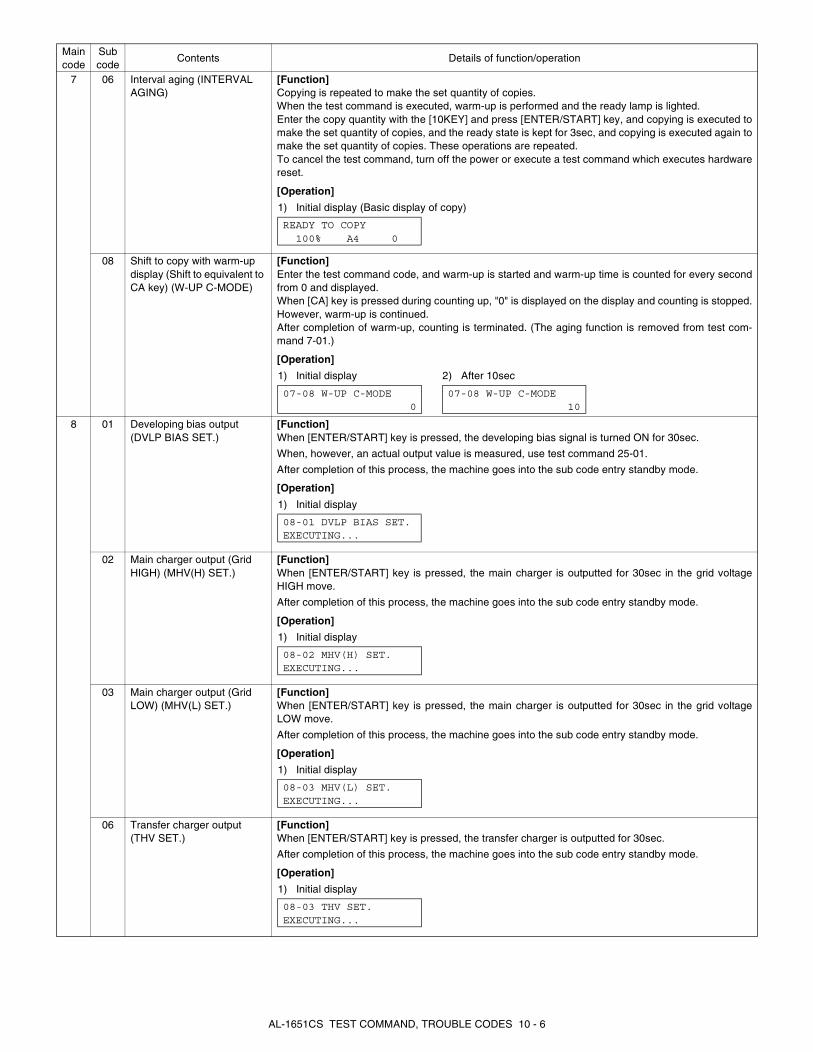
7 06 Interval aging (INTERVAL AGING)
[Function]Copying is repeated to make the set quantity of copies.When the test command is executed, warm-up is performed and the ready lamp is lighted.Enter the copy quantity with the [10KEY] and press [ENTER/START] key, and copying is executed tomake the set quantity of copies, and the ready state is kept for 3sec, and copying is executed again tomake the set quantity of copies. These operations are repeated.To cancel the test command, turn off the power or execute a test command which executes hardwarereset.
[Operation]
08 Shift to copy with warm-up display (Shift to equivalent to CA key) (W-UP C-MODE)
[Function]Enter the test command code, and warm-up is started and warm-up time is counted for every secondfrom 0 and displayed.When [CA] key is pressed during counting up, "0" is displayed on the display and counting is stopped.However, warm-up is continued.After completion of warm-up, counting is terminated. (The aging function is removed from test com-mand 7-01.)
[Operation]
8 01 Developing bias output (DVLP BIAS SET.)
[Function]When [ENTER/START] key is pressed, the developing bias signal is turned ON for 30sec.
When, however, an actual output value is measured, use test command 25-01.
After completion of this process, the machine goes into the sub code entry standby mode.
[Operation]
02 Main charger output (Grid HIGH) (MHV(H) SET.)
[Function]When [ENTER/START] key is pressed, the main charger is outputted for 30sec in the grid voltageHIGH move.
After completion of this process, the machine goes into the sub code entry standby mode.
[Operation]
03 Main charger output (Grid LOW) (MHV(L) SET.)
[Function]When [ENTER/START] key is pressed, the main charger is outputted for 30sec in the grid voltageLOW move.
After completion of this process, the machine goes into the sub code entry standby mode.
[Operation]
06 Transfer charger output (THV SET.)
[Function]When [ENTER/START] key is pressed, the transfer charger is outputted for 30sec.
After completion of this process, the machine goes into the sub code entry standby mode.
[Operation]
Main code
Sub code
Contents Details of function/operation
1) Initial display (Basic display of copy)
READY TO COPY 100% A4 0
1) Initial display 2) After 10sec
07-08 W-UP C-MODE 0
07-08 W-UP C-MODE 10
1) Initial display
08-01 DVLP BIAS SET.EXECUTING...
1) Initial display
08-02 MHV(H) SET.EXECUTING...
1) Initial display
08-03 MHV(L) SET.EXECUTING...
1) Initial display
08-03 THV SET.EXECUTING...
AL-1651CS TEST COMMAND, TROUBLE CODES 10 - 6

9 01 Duplex motor normal rotation check (DPLX ROT.)
[Function]Use the duplex motor Bios to drive the duplex motor in the normal direction (paper exit direction) for30sec.
After completion of this process, the machine goes into the sub code entry standby mode.
[Operation]
02 Duplex motor reverse rotation check (DPLX ROT.REV.)
[Function]Use the duplex motor Bios to drive the duplex motor in the reverse direction for 30sec.
After completion of this process, the machine goes into the sub code entry standby mode.
[Operation]
10 00 Toner motor operation (TONER MOTOR)
[Function]When [ENTER/START] key is pressed, the toner motor is rotated for 30sec.
After completion of this process, the machine goes into the main code entry standby mode.
[Operation]
14 00 Cancel of trouble other than U2 (TRBL CANC.)
[Function]Used to cancel troubles other than U2. ∗ Cancel troubles such as H trouble which writes data into EEPROM, and perform hardware reset.
[Operation]
16 00 U2 trouble cancel (U2 TRBL CANC.)
[Function]Used to cancel U2 trouble.
When [ENTER/START] key is pressed, check sum of the total counter in the EEPROM is rewrittenand hardware reset is made.
[Operation]
22 04 JAM total counter display (JAM TTL CNT)
[Function]The JAM total counter is displayed.
[Operation]
05 Total counter display (TTL CNT)
[Function]The total counter value is displayed.
[Operation]
08 SPF counter display (SPF CNT)
[Function]The SPF counter is displayed.
[Operation]
Main code
Sub code
Contents Details of function/operation
1) Initial display
09-01 DPLX ROT.EXECUTING...
1) Initial display
09-02 DPLX ROT.REV.EXECUTING...
1) Initial display
10-00 TONER MOTOREXECUTING...
1) Initial display
14-00 TRBL CANC.CLEARED
1) Initial display
16-00 U2 TRBL CANC.CLEARED
1) Initial display
22-04 JAM TTL CNT ***,***
1) Initial display
22-05 TTL CNT ***,***
1) Initial display
22-08 SPF CNT ***,***
AL-1651CS TEST COMMAND, TROUBLE CODES 10 - 7

22 12 Drum counter display (DRUM CNT)
[Function]The drum counter is displayed.
[Operation]
14 ROM version display (ROM VER.)
[Function]The P-ROM version is displayed. Press [←/→/10KEY] to switch the display version.
[Operation]
16 Duplex counter display (DPLX CNT)
[Function]The duplex counter is displayed.
[Operation]
17 Copy counter display (COPIES CNT)
[Function]The copy counter is displayed.
[Operation]
18 Printer counter display (PRT.CNT)
[Function]The printer counter is displayed.
[Operation]
19 Scanner mode counter display (S-MODE CNT)
[Function]The scanner mode counter is displayed.
[Operation]
21 Scanner counter display (SCAN CNT)
[Function]The scanner counter is displayed.
[Operation]
Main code
Sub code
Contents Details of function/operation
1) Initial display
22-12 DRUM CNT ***,***
Code number Version Display item0 Main unit Program MAIN PROG.1 IMC Program IMC PROG.2 FAX Program FAX PROG.3 LCD DATA LCD DATA
1) Initial display 2) [→/10KEY]
2) [←/10KEY]
22-14 ROM VER.MAIN PROG. 00.00
22-14 ROM VER.IMC PROG. 00.00
22-14 ROM VER.LCD DATA 00.00
1) Initial display
22-16 DPLX CNT ***,***
1) Initial display
22-17 COPIES CNT ***,***
1) Initial display
22-18 PRT.CNT ***,***
1) Initial display
22-19 S-MODE CNT ***,***
1) Initial display
22-21 SCAN CNT ***,***
AL-1651CS TEST COMMAND, TROUBLE CODES 10 - 8
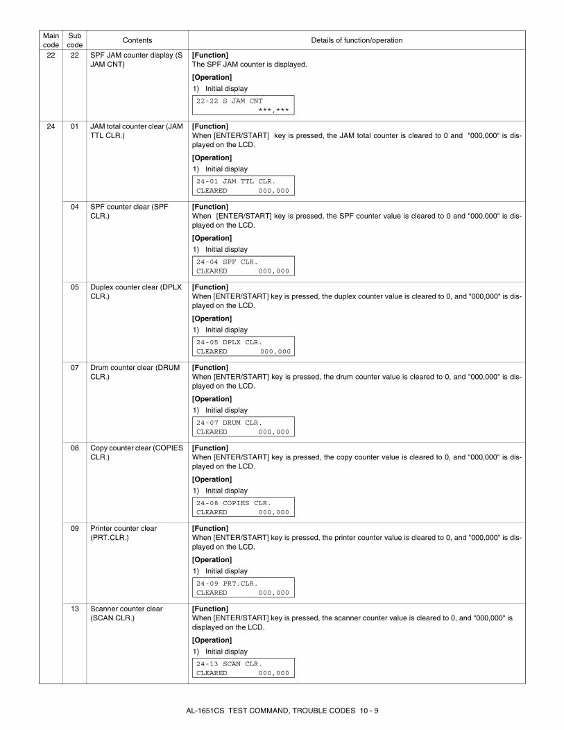
22 22 SPF JAM counter display (S JAM CNT)
[Function]The SPF JAM counter is displayed.
[Operation]
24 01 JAM total counter clear (JAM TTL CLR.)
[Function]When [ENTER/START] key is pressed, the JAM total counter is cleared to 0 and "000,000" is dis-played on the LCD.
[Operation]
04 SPF counter clear (SPF CLR.)
[Function]When [ENTER/START] key is pressed, the SPF counter value is cleared to 0 and "000,000" is dis-played on the LCD.
[Operation]
05 Duplex counter clear (DPLX CLR.)
[Function]When [ENTER/START] key is pressed, the duplex counter value is cleared to 0, and "000,000" is dis-played on the LCD.
[Operation]
07 Drum counter clear (DRUM CLR.)
[Function]When [ENTER/START] key is pressed, the drum counter value is cleared to 0, and "000,000" is dis-played on the LCD.
[Operation]
08 Copy counter clear (COPIES CLR.)
[Function]When [ENTER/START] key is pressed, the copy counter value is cleared to 0, and "000,000" is dis-played on the LCD.
[Operation]
09 Printer counter clear (PRT.CLR.)
[Function]When [ENTER/START] key is pressed, the printer counter value is cleared to 0, and "000,000" is dis-played on the LCD.
[Operation]
13 Scanner counter clear (SCAN CLR.)
[Function]When [ENTER/START] key is pressed, the scanner counter value is cleared to 0, and "000,000" is displayed on the LCD.
[Operation]
Main code
Sub code
Contents Details of function/operation
1) Initial display
22-22 S JAM CNT ***,***
1) Initial display
24-01 JAM TTL CLR.CLEARED 000,000
1) Initial display
24-04 SPF CLR.CLEARED 000,000
1) Initial display
24-05 DPLX CLR.CLEARED 000,000
1) Initial display
24-07 DRUM CLR.CLEARED 000,000
1) Initial display
24-08 COPIES CLR.CLEARED 000,000
1) Initial display
24-09 PRT.CLR.CLEARED 000,000
1) Initial display
24-13 SCAN CLR.CLEARED 000,000
AL-1651CS TEST COMMAND, TROUBLE CODES 10 - 9
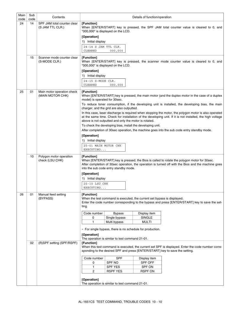
24 14 SPF JAM total counter clear (S JAM TTL CLR.)
[Function]When [ENTER/START] key is pressed, the SPF JAM total counter value is cleared to 0, and"000,000" is displayed on the LCD.
[Operation]
15 Scanner mode counter clear (S-MODE CLR.)
[Function]When [ENTER/START] key is pressed, the scanner mode counter value is cleared to 0, and"000,000" is displayed on the LCD.
[Operation]
25 01 Main motor operation check (MAIN MOTOR CHK)
[Function]When [ENTER/START] key is pressed, the main motor (and the duplex motor in the case of a duplexmodel) is operated for 30sec.
To reduce toner consumption, if the developing unit is installed, the developing bias, the maincharger, and the grid are also outputted.
In this case, laser discharge is required when stopping the motor, the polygon motor is also operatedat the same time. Check for installation of the developing unit. If it is not installed, the high voltageabove is not outputted and only the motor is rotated.
To check the developing bias, install the developing unit.
After completion of 30sec operation, the machine goes into the sub code entry standby mode.
[Operation]
10 Polygon motor operation check (LSU CHK)
[Function]When [ENTER/START] key is pressed, the Bios is called to rotate the polygon motor for 30sec. After completion of 30sec operation, the operation is turned off with the Bios and the machine goesinto the sub code entry standby mode.
[Operation]
26 01 Manual feed setting (BYPASS)
[Function]When the test command is executed, the current set bypass is displayed. Enter the code number corresponding to the bypass and press [ENTER/START] key to save the set-ting.
∗ For single bypass, there is no schedule for production.
[Operation]The operation is similar to test command 21-01.
02 (R)SPF setting (SPF/RSPF) [Function]When this test command is executed, the current set SPF is displayed. Enter the code number corre-sponding to the desired SPF and press [ENTER/START] key to save the setting.
[Operation]The operation is similar to test command 21-01.
Main code
Sub code
Contents Details of function/operation
1) Initial display
24-14 S JAM TTL CLR.CLEARED 000,000
1) Initial display
24-15 S-MODE CLR.CLEARED 000,000
1) Initial display
25-01 MAIN MOTOR CHKEXECUTING...
1) Initial display
25-10 LSU CHKEXECUTING...
Code number Bypass Display item0 Single bypass SINGLE1 Multi bypass MULTI
Code number SPF Display item0 SPF NO SPF OFF1 SPF YES SPF ON2 RSPF YES RSPF ON
AL-1651CS TEST COMMAND, TROUBLE CODES 10 - 10

26 03 Second cassette setting (2ND TRAY)
[Function]When this test command is executed, the current set second cassette is displayed. Enter the codenumber corresponding to the desired second cassette and press [ENTER/START] key to save thesetting.
[Operation]The operation is similar to test command 21-01.
04 Main unit duplex setting (DPLX)
[Function]When this test command is executed, the current set duplex is displayed. Enter the code number cor-responding to the desired duplex and press [ENTER/START] key to save the setting.
[Operation]The operation is similar to test command 21-01.
06 Destination setting (DESTINATION)
[Function]When this test command is executed, the current set destination is displayed. Enter the code number corresponding to the desired destination and press [ENTER/START] key to save the setting.
∗ For Japan AB series, there is no schedule for production.
[Operation]The operation is similar to test command 21-01.
07 Machine conditions check (CPM)
[Function]When this test command is executed, the current machine setting is displayed.
[Operation]
20 Rear edge void setting (END EDGE)
[Function]When this test command is executed, the current set rear edge void is displayed. Enter the code num-ber corresponding to the desired rear edge void and press [ENTER/START] key to save the setting.
[Operation]The operation is similar to test command 21-01.
Main code
Sub code
Contents Details of function/operation
Code number Second cassette Display item0 Second cassette NO OFF1 Second cassette YES ON
Code number Duplex Display item0 Duplex NO OFF1 Duplex YES ON
Code number Destination Display item0 Inch series INCH1 EX Japan AB series AB2 Japan AB series –3 China (EX Japan AB series + China paper support) CHINA
CPM Coy quantity Remark10 CPM 1012 CPM 1213 CPM 1314 CPM 1415 CPM 1516 CPM 16
1) The machine setting is displayed.
26-07 CPM10 CPM
Code number Setting Display item Remark0 Rear edge void NO OFF1 Rear edge void YES ON Default
AL-1651CS TEST COMMAND, TROUBLE CODES 10 - 11
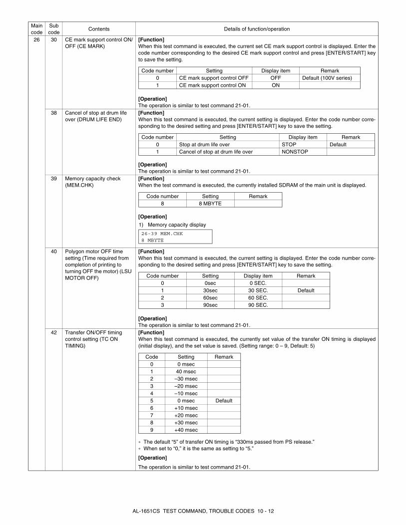
26 30 CE mark support control ON/OFF (CE MARK)
[Function]When this test command is executed, the current set CE mark support control is displayed. Enter thecode number corresponding to the desired CE mark support control and press [ENTER/START] keyto save the setting.
[Operation]The operation is similar to test command 21-01.
38 Cancel of stop at drum life over (DRUM LIFE END)
[Function]When this test command is executed, the current setting is displayed. Enter the code number corre-sponding to the desired setting and press [ENTER/START] key to save the setting.
[Operation]The operation is similar to test command 21-01.
39 Memory capacity check (MEM.CHK)
[Function]When the test command is executed, the currently installed SDRAM of the main unit is displayed.
[Operation]
40 Polygon motor OFF time setting (Time required from completion of printing to turning OFF the motor) (LSU MOTOR OFF)
[Function]When this test command is executed, the current setting is displayed. Enter the code number corre-sponding to the desired setting and press [ENTER/START] key to save the setting.
[Operation]The operation is similar to test command 21-01.
42 Transfer ON/OFF timing control setting (TC ON TIMING)
[Function]When this test command is executed, the currently set value of the transfer ON timing is displayed(initial display), and the set value is saved. (Setting range: 0 – 9, Default: 5)
∗ The default “5” of transfer ON timing is “330ms passed from PS release.”∗ When set to “0,” it is the same as setting to “5.”
[Operation]
The operation is similar to test command 21-01.
Main code
Sub code
Contents Details of function/operation
Code number Setting Display item Remark0 CE mark support control OFF OFF Default (100V series)1 CE mark support control ON ON
Code number Setting Display item Remark0 Stop at drum life over STOP Default1 Cancel of stop at drum life over NONSTOP
Code number Setting Remark8 8 MBYTE
1) Memory capacity display
26-39 MEM.CHK8 MBYTE
Code number Setting Display item Remark0 0sec 0 SEC.1 30sec 30 SEC. Default2 60sec 60 SEC.3 90sec 90 SEC.
Code Setting Remark0 0 msec1 40 msec2 –30 msec3 –20 msec4 –10 msec5 0 msec Default6 +10 msec7 +20 msec8 +30 msec9 +40 msec
AL-1651CS TEST COMMAND, TROUBLE CODES 10 - 12
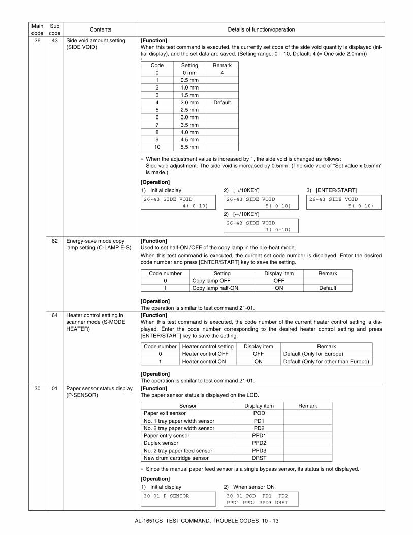
26 43 Side void amount setting (SIDE VOID)
[Function]When this test command is executed, the currently set code of the side void quantity is displayed (ini-tial display), and the set data are saved. (Setting range: 0 – 10, Default: 4 (= One side 2.0mm))
∗ When the adjustment value is increased by 1, the side void is changed as follows:Side void adjustment: The side void is increased by 0.5mm. (The side void of “Set value x 0.5mm”is made.)
[Operation]
62 Energy-save mode copy lamp setting (C-LAMP E-S)
[Function]Used to set half-ON /OFF of the copy lamp in the pre-heat mode.
When this test command is executed, the current set code number is displayed. Enter the desiredcode number and press [ENTER/START] key to save the setting.
[Operation]The operation is similar to test command 21-01.
64 Heater control setting in scanner mode (S-MODE HEATER)
[Function]When this test command is executed, the code number of the current heater control setting is dis-played. Enter the code number corresponding to the desired heater control setting and press[ENTER/START] key to save the setting.
[Operation]The operation is similar to test command 21-01.
30 01 Paper sensor status display (P-SENSOR)
[Function]The paper sensor status is displayed on the LCD.
∗ Since the manual paper feed sensor is a single bypass sensor, its status is not displayed.
[Operation]
Main code
Sub code
Contents Details of function/operation
9
Code Setting Remark0 0 mm 41 0.5 mm2 1.0 mm3 1.5 mm4 2.0 mm Default5 2.5 mm6 3.0 mm7 3.5 mm8 4.0 mm9 4.5 mm10 5.5 mm
1) Initial display 2) [→/10KEY]
2) [←/10KEY]
3) [ENTER/START]
26-43 SIDE VOID 4( 0-10)
26-43 SIDE VOID 5( 0-10)
26-43 SIDE VOID 3( 0-10)
26-43 SIDE VOID 5( 0-10)
Code number Setting Display item Remark0 Copy lamp OFF OFF1 Copy lamp half-ON ON Default
Code number Heater control setting Display item Remark0 Heater control OFF OFF Default (Only for Europe)1 Heater control ON ON Default (Only for other than Europe)
Sensor Display item RemarkPaper exit sensor PODNo. 1 tray paper width sensor PD1No. 2 tray paper width sensor PD2Paper entry sensor PPD1Duplex sensor PPD2No. 2 tray paper feed sensor PPD3New drum cartridge sensor DRST
1) Initial display 2) When sensor ON
30-01 P-SENSOR 30-01 POD PD1 PD2PPD1 PPD2 PPD3 DRST
AL-1651CS TEST COMMAND, TROUBLE CODES 10 - 13

41 06 OC cover float detection level (OC FLOAT LEVEL)
[Function]When this test command is executed, the current set value is displayed. When [ENTER/START] keyis pressed, the mirror base unit moves to the SPF scan position to acquire the OC cover float detec-tion level.
When the mirror base unit returns to the home position, the acquired value is displayed.
If the detection level is not acquired, ERR display is made. (Default: 0)
Note that, this test command must be executed with the OC cover closed.∗ If the value is 0, float detection is not performed in normal jobs.
[Operation]
43 01 Fusing temperature setting (Normal copy) (FU TEMP)
[Function]When this test command is executed, the current set code number is displayed. Press [←/→/10KEY]key to change the setting and press [ENTER/START] key to save the setting into the EERPOM. Themachine goes into the sub code entry standby mode.
[Operation]The operation is similar to test command 21-01.
04 Fusing temperature setting in multi coy (FU TEMP MULTI)
[Function]For 20th sheet or later in multi copy, the fusing temperature is automatically changed from the temper-ature set with test command 43-1 to the temperature set with this test command.
When this test command is executed, the current set code number is displayed. Enter the code num-ber and press [ENTER/START] key to change the setting.
[Operation]The operation is similar to test command 21-01.
Main code
Sub code
Contents Details of function/operation
1) Initial display
2) [ENTER/START]
41-06 OC FLOAT LEVEL 0
41-06 OC FLOAT LEVELEXECUTING...
<Canceling - when C/CA key is pressed->
After canceling, the machine goes into the sub code entrystandby mode.
3) When the level is acquired:
3) When the level is not acquired:
THE JOB IS BEINGCANCELED.
41-06 OC FLOAT LEVEL **** OK
41-06 OC FLOAT LEVEL **** ERR
Code Set temperature (°C) Remark0 1601 1652 1703 1754 1805 1856 190 Default7 1958 200
Code Set temperature (°C) Remark0 1551 1602 1653 170 Default4 1755 180
AL-1651CS TEST COMMAND, TROUBLE CODES 10 - 14
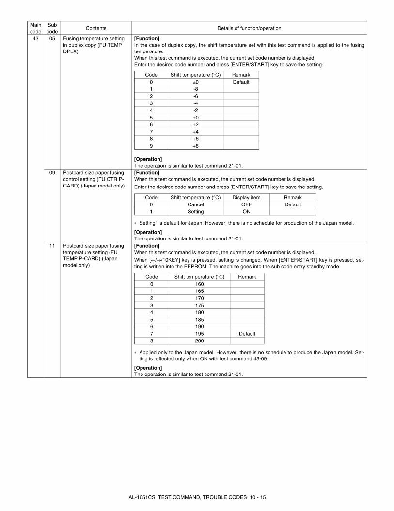
43 05 Fusing temperature setting in duplex copy (FU TEMP DPLX)
[Function]In the case of duplex copy, the shift temperature set with this test command is applied to the fusingtemperature.When this test command is executed, the current set code number is displayed. Enter the desired code number and press [ENTER/START] key to save the setting.
[Operation]The operation is similar to test command 21-01.
09 Postcard size paper fusing control setting (FU CTR P-CARD) (Japan model only)
[Function]When this test command is executed, the current set code number is displayed.
Enter the desired code number and press [ENTER/START] key to save the setting.
∗ Setting" is default for Japan. However, there is no schedule for production of the Japan model.
[Operation]The operation is similar to test command 21-01.
11 Postcard size paper fusing temperature setting (FU TEMP P-CARD) (Japan model only)
[Function]When this test command is executed, the current set code number is displayed.
When [←/→/10KEY] key is pressed, setting is changed. When [ENTER/START] key is pressed, set-ting is written into the EEPROM. The machine goes into the sub code entry standby mode.
∗ Applied only to the Japan model. However, there is no schedule to produce the Japan model. Set-ting is reflected only when ON with test command 43-09.
[Operation]The operation is similar to test command 21-01.
Main code
Sub code
Contents Details of function/operation
Code Shift temperature (°C) Remark0 ±0 Default1 -82 -63 -44 -25 ±06 +27 +48 +69 +8
Code Shift temperature (°C) Display item Remark0 Cancel OFF Default1 Setting ON
Code Shift temperature (°C) Remark0 1601 1652 1703 1754 1805 1856 1907 195 Default8 200
AL-1651CS TEST COMMAND, TROUBLE CODES 10 - 15
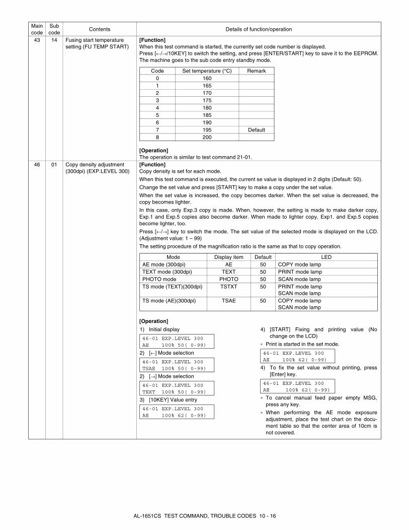
43 14 Fusing start temperature setting (FU TEMP START)
[Function]When this test command is started, the currently set code number is displayed.Press [←/→/10KEY] to switch the setting, and press [ENTER/START] key to save it to the EEPROM.The machine goes to the sub code entry standby mode.
[Operation]The operation is similar to test command 21-01.
46 01 Copy density adjustment (300dpi) (EXP.LEVEL 300)
[Function]Copy density is set for each mode.
When this test command is executed, the current se value is displayed in 2 digits (Default: 50).
Change the set value and press [START] key to make a copy under the set value.
When the set value is increased, the copy becomes darker. When the set value is decreased, thecopy becomes lighter.
In this case, only Exp.3 copy is made. When, however, the setting is made to make darker copy,Exp.1 and Exp.5 copies also become darker. When made to lighter copy, Exp1. and Exp.5 copiesbecome lighter, too.
Press [←/→] key to switch the mode. The set value of the selected mode is displayed on the LCD.(Adjustment value: 1 – 99)
The setting procedure of the magnification ratio is the same as that to copy operation.
[Operation]
Main code
Sub code
Contents Details of function/operation
Code Set temperature (°C) Remark0 1601 1652 1703 1754 1805 1856 1907 195 Default8 200
Mode Display item Default LEDAE mode (300dpi) AE 50 COPY mode lampTEXT mode (300dpi) TEXT 50 PRINT mode lampPHOTO mode PHOTO 50 SCAN mode lampTS mode (TEXT)(300dpi) TSTXT 50 PRINT mode lamp
SCAN mode lampTS mode (AE)(300dpi) TSAE 50 COPY mode lamp
SCAN mode lamp
1) Initial display
2) [←] Mode selection
2) [→] Mode selection
3) [10KEY] Value entry
4) [START] Fixing and printing value (Nochange on the LCD)
∗ Print is started in the set mode.
4) To fix the set value without printing, press[Enter] key.
∗ To cancel manual feed paper empty MSG,press any key.
∗ When performing the AE mode exposureadjustment, place the test chart on the docu-ment table so that the center area of 10cm isnot covered.
46-01 EXP.LEVEL 300AE 100% 50( 0-99)
46-01 EXP.LEVEL 300TSAE 100% 50( 0-99)
46-01 EXP.LEVEL 300TEXT 100% 50( 0-99)
46-01 EXP.LEVEL 300AE 100% 62( 0-99)
46-01 EXP.LEVEL 300AE 100% 62( 0-99)
46-01 EXP.LEVEL 300AE 100% 62( 0-99)
AL-1651CS TEST COMMAND, TROUBLE CODES 10 - 16
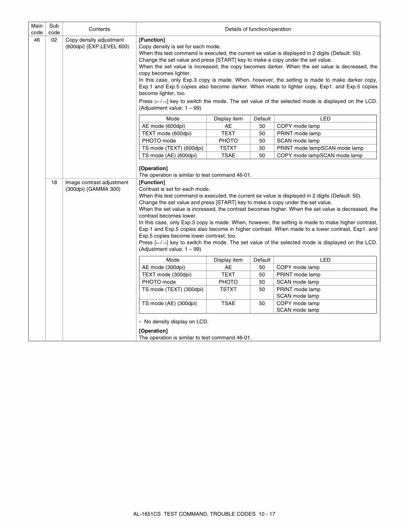
46 02 Copy density adjustment (600dpi) (EXP.LEVEL 600)
[Function]Copy density is set for each mode.When this test command is executed, the current se value is displayed in 2 digits (Default: 50).Change the set value and press [START] key to make a copy under the set value.When the set value is increased, the copy becomes darker. When the set value is decreased, thecopy becomes lighter.In this case, only Exp.3 copy is made. When, however, the setting is made to make darker copy,Exp.1 and Exp.5 copies also become darker. When made to lighter copy, Exp1. and Exp.5 copiesbecome lighter, too.
Press [←/→] key to switch the mode. The set value of the selected mode is displayed on the LCD.(Adjustment value: 1 – 99)
[Operation]The operation is similar to test command 46-01.
18 Image contrast adjustment (300dpi) (GAMMA 300)
[Function]Contrast is set for each mode.When this test command is executed, the current se value is displayed in 2 digits (Default: 50).Change the set value and press [START] key to make a copy under the set value.When the set value is increased, the contrast becomes higher. When the set value is decreased, thecontrast becomes lower.In this case, only Exp.3 copy is made. When, however, the setting is made to make higher contrast,Exp.1 and Exp.5 copies also become in higher contrast. When made to a lower contrast, Exp1. andExp.5 copies become lower contrast, too.Press [←/→] key to switch the mode. The set value of the selected mode is displayed on the LCD.(Adjustment value: 1 – 99)
∗ No density display on LCD.
[Operation]The operation is similar to test command 46-01.
Main code
Sub code
Contents Details of function/operation
Mode Display item Default LEDAE mode (600dpi) AE 50 COPY mode lampTEXT mode (600dpi) TEXT 50 PRINT mode lampPHOTO mode PHOTO 50 SCAN mode lampTS mode (TEXT) (600dpi) TSTXT 50 PRINT mode lampSCAN mode lampTS mode (AE) (600dpi) TSAE 50 COPY mode lampSCAN mode lamp
Mode Display item Default LEDAE mode (300dpi) AE 50 COPY mode lampTEXT mode (300dpi) TEXT 50 PRINT mode lampPHOTO mode PHOTO 50 SCAN mode lampTS mode (TEXT) (300dpi) TSTXT 50 PRINT mode lamp
SCAN mode lampTS mode (AE) (300dpi) TSAE 50 COPY mode lamp
SCAN mode lamp
AL-1651CS TEST COMMAND, TROUBLE CODES 10 - 17

46 19 Exposure mode setting (AE MODE)
[Function]<γ table setting>
When this test command is executed, the code number of the current set gamma table is displayed.(Default: Japan -1/Ex Japan -2)Enter the code number corresponding to the desired gamma table, and press [←/→] key to changethe mode and write into the EEPROM.
<AE operation mode>
When setting the γ table, press [→] key to change to the AE operation mode, and the current set codenumber of the AE operation mode is displayed. (Default: 0)Enter the code number corresponding to the desired AE operation mode and press [←/→] key tochange the mode and write into the EEPROM.
<PHOTO image process setting>
When [→] key is pressed in AE operation mode setting, the mode is changed to the PHOTO imageprocess setting and the code number of the current set PHOTO image process setting is displayed.(Default: 0)Enter the code number corresponding to the desired PHOTO image process setting and press [←/→]key to change the mode and write into the EEPROM.
[Operation]
20 SPF exposure correction (EXP.LEVEL SPF)
[Function]Used to adjust the exposure correction amount in the SPF mode. The adjustment is made by adjust-ing Vref voltage variation for the OC mode.
When this test command is executed, the current set value is displayed in 2 digits (Default: 50).Change the set value and press [START] key to save the setting and make a copy.
When the set value is increased, copy becomes darker. When the set value is decreased, copybecomes lighter. (Adjustment range: 1 – 99)
[Operation]The operation is similar to test command 46-01.
Main code
Sub code
Contents Details of function/operation
Mode Display item Code number Setting content Remark
γ GAMMA1 Image quality priority mode Japan default2 Toner consumption priority mode EX Japan default
AE AE0 Lead edge stop Default1 Real time process
PHOTO PHOTO1 Error diffusion process Default2 Dither process
1) Initial display <γ table setting>
2) [→] Mode selection
2) [←] Mode selection
3) [10KEY] Value input
4) [ENTER/START] Save theset value. The machinegoes to the sub code entrystandby mode.
46-19 AE MODEGAMMA 2( 1-2)
46-19 AE MODEAE 0( 0-1)
46-19 AE MODEPHOTO 1( 1-2)
46-19 AE MODEAE 1( 0-1)
Mode Display item Default RemarkSPF SPF 50
AL-1651CS TEST COMMAND, TROUBLE CODES 10 - 18
46 29 Image contrast adjustment (600dpi) (GAMMA 600)
[Function]Contrast is set for each mode.
When this test command is executed, the current se value is displayed in 2 digits (Default: 50).
Change the set value and press [START] key to make a copy under the set value.
When the set value is increased, the contrast becomes higher. When the set value is decreased, thecontrast becomes lower.
In this case, only Exp.3 copy is made. When, however, the setting is made to make higher contrast,Exp.1 and Exp.5 copies also become in higher contrast. When made to a lower contrast, Exp1. andExp.5 copies become lower contrast, too.
Press [←/→] key to switch the mode. The set value of the selected mode is displayed on the LCD.(Adjustment value: 1 – 99)
∗ No density display on LCD.
[Operation]The operation is similar to test command 46-01.
30 AE limit adjustment (AE LIMIT)
[Function]Used to set the limit value in AE and AE (toner save).Change the setting and press [ENTER/START] key to write the setting into the EEPROM. Themachine goes into the sub code entry standby mode.By pressing [←/→] key, setting is changed. (Setting range: 0 – 31, Default: 0)
<Remark>
When test command 26-06 (Destination setting) or test command 46-19 Auto Exposure mode ischanged, the setting of this test command is also changed to the default in connection.
[Operation]The operation is similar to test command 46-19.
31 Image sharpness adjustment (SHARPNESS)
[Function]Used to adjust sharpening/blurring of image in each mode.
When this test command is executed, warm-up and shading are performed and the current set valueis displayed. (Default: 1)Change the set value and press [START] key to make a copy under the set conditions.To change the mode, press [←/→] key. The code number of the selected mode is dip0slayed on theLCD.
[Operation]The operation is similar to test command 46-01.
Main code
Sub code
Contents Details of function/operation
Mode Display item Default LEDAE mode (600dpi) AE 50 COPY mode lampTEXT mode (600dpi) TEXT 50 PRINT mode lampPHOTO mode PHOTO 50 SCAN mode lampTS mode (TEXT)(600dpi) TSTXT 50 PRINT mode lamp
SCAN mode lampTS mode (AE)(600dpi) TSAE 50 COPY mode lamp
SCAN mode lamp
Mode Display item RemarkLimit value for AE AELimit value for AE (toner save) TSAE
Image quality Setting No RemarkBlurring 0
Standard 1 DefaultSharpening 2
Mode Display item Default setting LEDAE mode AE 1 COPY mode lampTEXT mode TEXT 1 PRINT mode lampPHOTO mode PHOTO 1 SCAN mode lampTS mode (TEXT) TSTXT 1 PRINT mode lamp
SCAN mode lampTS mode (AE) TSAE 1 COPY mode lamp
SCAN mode lamp
AL-1651CS TEST COMMAND, TROUBLE CODES 10 - 19
46 32 Copier color reproduction setting (COLOR REAPPEAR)
[Function]Used to set color reproduction in each mode. Colors easy to be copied and colors difficult to be copiedcan be switched.
∗ This setting has virtually no effect on black-and-white documents.
When this test command is executed, warm-up and shading are performed and the current set valueis displayed. (Default: 0)Press [START] key to make a copy under the set conditions . At that time, color components arechanged for used in copying.To change the mode, press [←/→] key. The code number of the selected mode is dip0slayed on theLCD.
[Operation]The operation is similar to test command 46-01.
48 01 Main scan/sub scan direction magnification ratio (COPY MAG.)
[Function]Used to adjust the magnification ratio in the main scan (front/rear) direction and sub scan direction.Enter the adjustment value with [10KEY]. Press [START] key to save the set value and make a copy.(When the adjustment value is increased by 1, the magnification ratio is increased by 0.1%.)The adjustment mode can be changed by pressing [←/→] key. (Adjustment range: 1 – 99, Default: 50)
[Operation]The operation is similar to test command 46-01.
05 SPF/RSPF mode sub scan direction magnification ratio in copying (SPF/RSPF MAG.)
[Function]Used to display the current SPF/RSPF mode sub scan direction magnification ratio on the LCD. When [START] key is pressed, the entered data is acquired and saved into the EEPROM, and a copyis made. (When the set value is increased by 1, the magnification ratio is increased by 0.1%.) (Adjustment range: 1 – 99, Default: 50)
When adjusting the RSPF, use [2-SIDED COPY] key to select single/duplex after entering the onepage print mode, performing 2-page single copy.
For printing, regardless of the density mode and the density level,
Density mode = MANUALDensity level = 3
∗ When there is no document in SPF, copy is inhibited.
[Operation]The operation is similar to test command 46-01.
Main code
Sub code
Contents Details of function/operation
Set value Colors easy to be copied Colors difficult to be copied0 Purple, Blue, Red Yellow, Green, Water blue1 Water blue, Green, Blue Purple, Red, Yellow2 Yellow, Red, Green Blue, Water blue, Purple
Specification component Setting No RemarkGreen 0 DefaultRed 1Blue 2
Mode Display item Default setting LEDAE mode (including TS) AE 0 COPY mode lampTEXT mode (including TS) TEXT 0 PRINT mode lampPHOTO mode PHOTO 0 SCAN mode lamp
Mode Display item Default value LEDMain scan direction magnification ratio F-R 50 PRINT mode lampOC mode sub scan direction magnification ratio
SCAN 50 SCAN mode lamp
Mode Display item Default LEDSub scan magnification ratio adjustment on the surface of SPF/RSPF document
SIDE1 50 COPY mode lamp
Sub scan magnification ratio adjustment on the surface of RSPF document
SIDE2 50 PRINT mode lamp
AL-1651CS TEST COMMAND, TROUBLE CODES 10 - 20

49 01 Download mode (DOWNLOAD MODE)
[Function]When this test command is executed, "DLOWNLOAD MODE" is displayed on the LCD and themachine goes into the program writing mode from PC to Flash ROM.
Use the writing tool on the PC and write the program.
During writing, the display shows as follows:
After completion of download, turn OFF/ON the power to reset.
In case of an error in download, the following message is displayed on the LCD.
To enter the download mode, there is a method to use key operations as well as to use a test com-mand. With the power OFF, press and hold [CA] + [←], turn on the power.
[Operation]
Main code
Sub code
Contents Details of function/operation
Status Display itemDownload data receiving RECEIVINGLoader function transfer LOADER COPYINGDate delete start FLASH ERASEData write (Boot section) BOOT WRITINGData write (Program section) PROGRAM WRITINGData write (EEPROM) E2PROM WRITINGData write (LCD) LCD DATE WRITINGDuring SUM CHECK FLASH ROM SUM CHECKDuring BOOT SUM CHECK BOOT SUM CHECKDuring EEPROM SUM CHECK EEPROM SUM CHECKDownload complete DOWNLOAD COMPLETE!
Error status Display itemPC data receiving E-01 PC TRANSLoader function transfer E-02 LOADER COPYFLASH ROM delete E-03 FLASH ERASEBoot section FLASH ROM write E-04 BOOT WRITEProgram section FLASH ROM write E-05 PROGRAM WRITELoader section SUM CHECK E-06 LOADER SUMBoot section SUM CHECK E-07 BOOT SUMProgram section SUM CHECK E-08 PROGRAM SUME2PROM SUM CHECK E-09 E2PROM SUME2PROM write E-10 E2PROM WRITEE2PROM read Verify E-11 E2PROM READE2PROM collating Verify E-12 E2PROM COLLATEBoot section lens check E-13 BOOT LENGTHProgram section lens check E-14 PROGRAM LENGTHE2PROM lens check E-15 E2PROM LENGTHTotal data size check E-16 DATE SIZEIMC communication error E-17 IMC TRANSIMC FRASH ROM write E-18 IMC FLASH WRITELCD section lens check E-19 LCD DATE LENGTHLCD section FLASH ROM write E-20 LCD DATE WRITELCD section SUM CHECK E-21 LCD DATE SUM
1) Initial display
DOWNLOAD MODE
AL-1651CS TEST COMMAND, TROUBLE CODES 10 - 21
50 01 Lead edge image position (LEAD EDGE)
[Function]Used to adjust the copy image position and the lead edge void amount on copy paper. The adjust-ment is made by adjusting the image scan start position at 100% and the print start position (resistroller ON timing). When this test command is executed, the current set value is displayed in 2 digits.(Center value: 50)
When [←/→] key is pressed, the setting mode and the display are changed.
Enter the adjustment value and press [START] key to save the set value and make a copy.
When the adjustment is made by the main cassette paper feed, the adjustment values of all the paperfeed ports become the same. (When the set value is increased by 1, shift is made by 0.1mm.)
(*): Support for the installation models. For non-installation models, skip.
[Adjustment procedure]1) Set the print start position (A: COPY mode lamp ON), the lead edge void amount (B: PRINT mode
lamp ON), the scan start position (C: SCAN mode lamp) to zero, and make a copy of the scale at100%.
2) Measure the image loss (Rmm) of the scale.
Set C = 10 x R (mm). (Example: Set to 40.)
When the value of C is increased by 10, the image loss is decreased by 1mm. (Default: 50)
3) Measure the distance (Hmm) from the paper lead edge to the image print start position.
Set A = 10 x H (mm). (Example: Set to 50.)
When the value of A is increased by 10, the image lead edge is moved to the paper lead edge by1mm. (Default: 50).
4) Set the lead edge void amount to B = 50 (2.5mm). (Default: 50)
When the value of B is increased by 10, the void is extended by about 0.1mm. (For 25 or less,however, the void amount is regarded as 0.)
∗ The SFP adjustment is made by adjusting the SPF image scan start position after OC adjustment.∗ When paper is discharged, the shifter is operated.
(Example)
[Operation]The operation is similar to test command 46-01.
Main code
Sub code
Contents Details of function/operation
Mode Display item Default LEDPrint start position (Main cassette paper feed)
TRAY1 50 COPY mode lampMain cassette lamp
(*) Print start position (2nd cassette paper feed)
TRAY2 50 COPY mode lamp2nd cassette lamp
Print start position (Manual paper feed)
MFT 50 COPY mode lampManual feed lamp
Image lead edge void amount DEN-A 50 PRINT mode lampImage scan start position RRC-A 50 SCAN mode lampImage rear edge void amount DEN-B 50 COPY mode lamp
PRINT mode lampSCAN mode lamp
5mm
10mm
Distance from the paper lead edge to the image lead edge, H = 5mm
Image loss, R = 4mm
AL-1651CS TEST COMMAND, TROUBLE CODES 10 - 22
50 06 Copy lead edge position adjustment (SPF/RSPF) (SPF/RSPF EDGE)
[Function]Used to adjust the SPF copy lead edge.
When the adjustment value of the document scan position adjustment is increased by 1, the scanstart timing is advanced by 0.1mm.
The print result is shifted to the opposite direction of the scan start position.
The adjustment mode can be changed by pressing [←/→] key. (Adjustment range: 1 – 99, Default:50)
When scanning a back surface of document, the mode must be changed to operate the RSPF bypressing [2-SIDED COPY] key.
∗ When there is no document in the SPF, copy is inhibited.∗ When paper is discharged, the shifter is operated.
[Operation]The operation is similar to test command 46-01.
10 Print center offset adjustment (PRT.OFF-CENTER)
[Function]Used to adjust the center offset position of copy images on copy paper and that in scanning docu-ment.When this test command is executed, the current set value is displayed.Enter the adjustment value and press [START] key to save the setting and make a copy. (When theset value is changed by 1, the center is shifted by 0.1mm.)When the adjustment value is increased, the center is shifted to right. When decreased, the center isshifted to left.The modes can be selected by pressing [←/→] key.When the set value is changed largely, the area outside the shading area may be scanned to causeblack streaks on the edges. When the RSPF is used, select the mode for use of the RSPF by [2-SIDED COPY] key.
(*) : Support for the installation models. For non-installation models, skip.∗ In the 2nd print center offset adjustment, print is made forcibly as 1to2/Short Edge from OC regard-
less of duplex setting.
∗ When paper is discharged, the shifter is operated.
[Operation]The operation is similar to test command 46-01.
12 Document feed off-center adjustment (ORG.OFF-CENTER)
[Function]Used to adjust document scan off-center adjustment. The adjustment modes can be selected by pressing [←/→] key. (Adjustment range: 1 – 99, Default:50) When the adjustment value is increased, the print result is shifted to left.
∗ When paper is discharged, the shifter is operated.
[Operation]The operation is similar to test command 46-01.
Main code
Sub code
Contents Details of function/operation
Mode Display item Default LEDFront surface document scan position adjustment
SIDE1 50 COPY mode lamp
Back surface document scan position adjustment
SIDE2 50 PRINT mode lamp
Rear edge void adjustment (SPF) END 50 SCAN mode lamp
Mode Display item Default LEDPrint center offset (Main cassette paper feed)
TRAY1 50 COPY mode lampMain cassette lamp
(*) Print center offset (2nd cassette paper feed)
TRAY2 50 COPY mode lamp2nd cassette lamp
Print center offset (Manual paper feed) MFT 50 COPY mode lampManual feed lamp
2nd print center offset (Main cassette paper feed)
SIDE2 50 PRINT mode lampMain cassette lamp
Mode Display item Default LEDPlaten document scan OC 50 COPY mode lampSPF document front scan SPF 50 PRINT mode lampRSPF document back scan RSPF 50 SCAN mode lamp
AL-1651CS TEST COMMAND, TROUBLE CODES 10 - 23
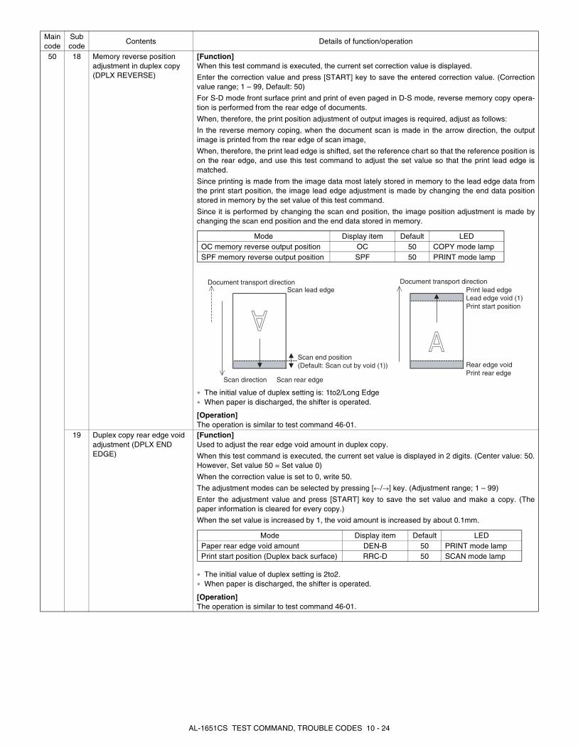
50 18 Memory reverse position adjustment in duplex copy (DPLX REVERSE)
[Function]When this test command is executed, the current set correction value is displayed.
Enter the correction value and press [START] key to save the entered correction value. (Correctionvalue range; 1 – 99, Default: 50)
For S-D mode front surface print and print of even paged in D-S mode, reverse memory copy opera-tion is performed from the rear edge of documents.
When, therefore, the print position adjustment of output images is required, adjust as follows:
In the reverse memory coping, when the document scan is made in the arrow direction, the outputimage is printed from the rear edge of scan image,
When, therefore, the print lead edge is shifted, set the reference chart so that the reference position ison the rear edge, and use this test command to adjust the set value so that the print lead edge ismatched.
Since printing is made from the image data most lately stored in memory to the lead edge data fromthe print start position, the image lead edge adjustment is made by changing the end data positionstored in memory by the set value of this test command.
Since it is performed by changing the scan end position, the image position adjustment is made bychanging the scan end position and the end data stored in memory.
∗ The initial value of duplex setting is: 1to2/Long Edge∗ When paper is discharged, the shifter is operated.
[Operation]The operation is similar to test command 46-01.
19 Duplex copy rear edge void adjustment (DPLX END EDGE)
[Function]Used to adjust the rear edge void amount in duplex copy.
When this test command is executed, the current set value is displayed in 2 digits. (Center value: 50.However, Set value 50 = Set value 0)
When the correction value is set to 0, write 50.
The adjustment modes can be selected by pressing [←/→] key. (Adjustment range; 1 – 99)
Enter the adjustment value and press [START] key to save the set value and make a copy. (Thepaper information is cleared for every copy.)
When the set value is increased by 1, the void amount is increased by about 0.1mm.
∗ The initial value of duplex setting is 2to2.∗ When paper is discharged, the shifter is operated.
[Operation]The operation is similar to test command 46-01.
Main code
Sub code
Contents Details of function/operation
Mode Display item Default LEDOC memory reverse output position OC 50 COPY mode lampSPF memory reverse output position SPF 50 PRINT mode lamp
Document transport direction Document transport directionScan lead edge Print lead edge
Lead edge void (1)Print start position
Scan end position(Default: Scan cut by void (1)) Rear edge void
Print rear edgeScan direction Scan rear edge
Mode Display item Default LEDPaper rear edge void amount DEN-B 50 PRINT mode lampPrint start position (Duplex back surface) RRC-D 50 SCAN mode lamp
AL-1651CS TEST COMMAND, TROUBLE CODES 10 - 24
51 02 Resist amount adjustment (RESIST ADJ.)
[Function]Used to adjust the contact pressure of the main unit resist roller and the RSPF resist roller onto paper.When this test command is executed, the current set value is displayed.
The adjustment modes can be selected by pressing [←/→] key.
Enter the adjustment value with [10KEY] and press [START] key to save the set value and make acopy.
(*): Support for the installation models. For non-installation models, skip.
[Operation]The operation is similar to test command 46-01.
53 08 SPF scan position automatic adjustment (SPF AUTO)
[Function]Place a black chart so that it covers the SPF scan glass and the OC glass together, and close the OCcover.
When this test command is executed, the current adjustment value is displayed as the initial display.
∗ Default is 1. Adjustment range is 1 – 99. Adjustment unit 1 = about 0.127mm
∗ If the values are kept as the default values, SPF scan is not performed properly. The front area ofthe proper scan position may be scanned.
In case of AUTO, press [START] key, and the mirror unit scans from the home position to the SPFscan position with the adjustment value displayed. The SPF glass cover edge position is calculatedfrom the difference between the SPFG glass cover edge and the OC side document glass CCD out-put level. If the adjustment is normal, the adjusted value is displayed. If abnormal, the error LED lightsup with the current set value displayed.
During the error LED is lighted, when [START] key is pressed again, execution is performed again.
[Operation]The operation is similar to test command 46-01. (In MANUAL)
OK/ERR display in AUTO
61 03 HSYNC output check (LSU CHK)
[Function]When [ENTER/START] key is pressed, HSYNC is performed and the polygon motor is rotated for 30sec. At that time, the COPY mode lamp is lighted for 100msec every time when HSYNC is detected.
[Operation]
Main code
Sub code
Contents Details of function/operation
Mode Display item Default LEDMain cassette paper fed TRAY1 50 COPY mode lamp
Main cassette lamp(*) 2nd cassette paper feed TRAY2 50 COPY mode lamp
2nd cassette lampManual paper feed MFT 50 COPY mode lamp
Manual feed lampRSPF document paper feed (Front surface)
SIDE1 50 COPY mode lampPRINT mode lampSCAN mode lamp
RSPF document paper feed (Back surface)
SIDE2 50 COPY mode lampPRINT mode lamp
Duplex back surface DUP-2 50 PRINT mode lampSCAN mode lamp
Mode Display item Default LEDSPF scan position auto adjustment AUTO 1 COPY mode lampSPF scan position manual adjustment MANU 1 PRINT mode lamp
<When OK> <When ERR>
53-08 SPF AUTOAUTO 100% ** OK
53-08 SPF AUTOAUTO 100% ** ERR
1) Initial display
61-03 LSU CHKEXECUTING...
AL-1651CS TEST COMMAND, TROUBLE CODES 10 - 25

63 01 Shading check (SHADING CHK)
[Function]Used to display the detection level of white plate for shading.
When [ENTER/START] key is pressed, the mirror base unit moves to the white plate for shading andthe copy lamp is lighted.
When the light quantity is stabilized, revision is made for every second, and the level of one pixel atthe center of CCD which is not corrected is detected and the value is displayed in decimal values onthe LCD. (3 digits)
[Operation]
02 Black level automatic correction (BLACK LEVEL)
[Function]Used to acquire the black level target value used for the black level adjustment of white balance.
When this test command is executed, the current correction value is displayed in 3 digits of 12bithexadecimal number.
Place the gray gradation chart (UKOG-0162FCZZ) used as the correction document so that the den-sity 10 (black side) comes on the left side and that the chart is upside down at the center of the plateleft center.
When [ENTER/START] key is pressed, the mirror base unit scans the chart and calculates the correc-tion value.
After completion of correction, the corrected value is displayed on the LCD.
∗ Default: 0
∗ If the value is set to the default, operation is made with 0x60.
[Operation]
Main code
Sub code
Contents Details of function/operation
1) Initial display
63-01 SHADING CHKEXECUTING... 000
Chart back surface
10
1) Initial display
2) [ENTER/START] Correction start
63-02 BLACK LEVEL 0
63-02 BLACK LEVELEXECUTING...
<During canceling - When C/CA is pressed->
After canceling, the machine goes into the sub code entrystandby mode.
3) After execution
3) In case of an error
THE JOB IS BEINGCANCELED.
63-02 BLACK LEVEL *** OK
63-02 BLACK LEVEL *** ERR
AL-1651CS TEST COMMAND, TROUBLE CODES 10 - 26
5. Trouble codesA. Trouble codes list B. Details of trouble codes
64 01 Self print (1by2 mode) (SELF PRT.)
[Function]The status of the optical section is ignored and printing of one page is made. Also when the print com-mand is received from the host, printing is made.
When this test command is executed, warm-up is performed and the ready lamp is lighted. (Since,however, the scanner is disabled, initializing is not made.)
Enter the code number and press [ENTER/START] key to start paper feed from the selected cassetteand print in the selected pattern.
∗ For 4 – 99, flip.
[Operation]The operation is similar to test command 21-01.
Main code
Sub code
Contents Details of function/operation
Code number Pattern Display item0 1by2 1 BY 21 Grid pattern CHECK2 White paper WHITE3 Black background BLACK
Main code
Sub code
Details of trouble
E1 00 IMC communication trouble10 IMC trouble13 IMC flash ROM error16 IMC DIMM memory read/write check error81 IMC communication interface error (parity)82 IMC communication interface error (Overrun)84 IMC communication interface error (Framing)
E7 02 LSU trouble10 Shading trouble (Black correction)11 Shading trouble (White correction)16 Abnormal laser output
F5 02 Copy lamp lighting abnormalityH2 00 Thermistor openH3 00 Heat roller high temperature detectionH4 00 Heat roller low temperature detectionL1 00 Feeding is not completed within the specified time after
starting feeding. (The scan head locking switch is locked)L3 00 Scanner return troubleL4 01 Main motor lock detectionL6 10 Polygon motor lock detectionU2 04 EEPROM read/write error (Serial communication error)
11 Counter check sum error (EEPROM)U9 99 Operation panel language error
Main code
Sub code
Details of trouble
E1 00 Content IMC communication troubleDetail An abnormality occurs in communication
between the CPU and the IMC.Cause IMC – CPU signal line abnormality
IMC Memory defect/data abnormalityCheck and remedy
Replace the MCU PWB with new one.
10 Content IMC troubleDetail An abnormality occurs in the IMC.Cause USB chip error/CODEC error on the IMC.Check and remedy
Replace the MCU PWB with a new one.
13 Content IMC flash ROM errorDetail An abnormality occurs in the IMC flash ROM.Cause IMC abnormalityCheck and remedy
Replace the MCU PWB with a new one.If downloading of the program is abnormally terminated, it may cause an error. Download the program again to avoid this.
16 Content IMC DIMM memory read/write check errorDetail An installation error occurs in the IMC memory
module.An error occurs during access to the IMC memory.
Cause Improper installation of the IMC memory module.IMC memory module abnormalityIMC memory contact abnormalityIMC abnormality.
Check and remedy
Check installation of the memory module.Replace the memory module.Replace the MCU PWB with a new one.
81 Content IMC communication interface error (parity)Detail A parity error occurs in communication between
the CPU and the IMC.Cause IMC memory defect/data abnormalityCheck and remedy
Check the memory of the IMC.Replace the MCU PWB with new one.
AL-1651CS TEST COMMAND, TROUBLE CODES 10 - 27
E1 82 Content IMC communication interface error (Overrun)Detail An overrun error occurs in communication
between the CPU and the IMC.Cause IMC memory defect/data abnormality.Check and remedy
Check the memory of the IMC.Replace the MCU PWB with new one.
84 Content IMC communication interface error (Framing)Detail A framing error occurs in communication
between the CPU and the IMC.Cause IMC memory defect/data abnormality.Check and remedy
Check the memory of the IMC.
E7 02 Content LSU troubleDetail The BD signal from the LSU cannot be detected
in a certain cycle. (Always OFF or always ON)Cause LSU connector or LSU harness defect or
disconnectionPolygon motor rotation abnormalityLaser beams are not generated.MCU PWB abnormality.
Check and remedy
Check connection of the LSU connector.Execute TC 61-03 to check the LSU operations.Check that the polygon motor rotates normally.Check that the laser emitting diode generates laser beams.Replace the LSU unit.Replace the MCU PWB.
10 Content Shading trouble (Black correction)Detail The CCD black scan level is abnormal when the
shading.Cause Improper connection of the CCD unit flat cable
CCD unit abnormalityMCU PWB abnormality
Check and remedy
Check connection of the CCD unit flat cable.Check the CCD unit.
11 Content Shading trouble (White correction)Detail The CCD white scan level is abnormal when the
shading.Cause Improper connection of the CCD unit flat cable
Dirt on the mirror, the lens, and the reference white plateCopy lamp lighting abnormalityCCD unit abnormalityMCU PWB abnormality(When occurred in the SPF scan position.)Improper installation of the mirror unit
Check and remedy
Clean the mirror, lens, and the reference white plate.Check the light quantity and lighting status of the copy lamp (TC 05-03).Check the MCU PWB.
16 Content Abnormal laser outputDetail When the laser output is stopped, HSYNC is
detected.Cause Laser abnormality
MCU PWB abnormality.Check and remedy
Check the laser emitting diode operation.Replace the MCU PWB.
Main code
Sub code
Details of trouble
F5 02 Content Copy lamp lighting abnormalityDetail The copy lamp does not turn on.Cause Copy lamp abnormality
Copy lamp harness abnormalityCCD PWB harness abnormality.
Check and remedy
Use TC 5-3 to check the copy lamp operations.When the copy lamp lights up.Check the harness and the connector between the CCD unit and the MCU PWB.When the copy lamp does not light up.Check the harness and the connector between the copy lamp unit and the MCU PWB.Replace the copy lamp unit.Replace the MCU PWB.
H2 00 Content Thermistor openDetail The thermistor is open.
The fusing unit is not installed.Cause Thermistor abnormality
Control PWB abnormalityFusing section connector disconnectionThe fusing unit is not installed.
Check and remedy
Check the harness and the connector between the thermistor and the PWB.Use TC 14 to clear the self diagnostic display.
H3 00 Content Heat roller high temperature detectionDetail The fusing temperature exceeds 240°C.Cause Thermistor abnormality
Control PWB abnormalityFusing section connector disconnection.
Check and remedy
Use TC 5-02 to check the heater lamp blinking operation.When the lamp blinks normally.Check the thermistor and its harness.Check the thermistor input circuit on the control PWB.When the lamp keeps ON.Check the power PWB and the lamp control circuit on the MCU PWB.Use TC 14 to clear the self diagnostic display.
H4 00 Content Heat roller low temperature detectionDetail The fusing temperature does not reach 185°C
within 27 sec of turning on the power, or the fusing temperature keeps at 140°C.
Cause Thermistor abnormalityHeater lamp abnormalityThermostat abnormalityControl PWB abnormality
Check and remedy
Use TC 5-02 to check the heater lamp blinking operation.When the lamp blinks normally.Check the thermistor and its harness.Check the thermistor input circuit on the control PWB.When the lamp does not light up.Check for disconnection of the heater lamp and the thermostat. Check the interlock switch.Check the power PWB and the lamp control circuit on the MCU PWB.Use TC 14 to clear the self diagnostic display.
Main code
Sub code
Details of trouble
AL-1651CS TEST COMMAND, TROUBLE CODES 10 - 28
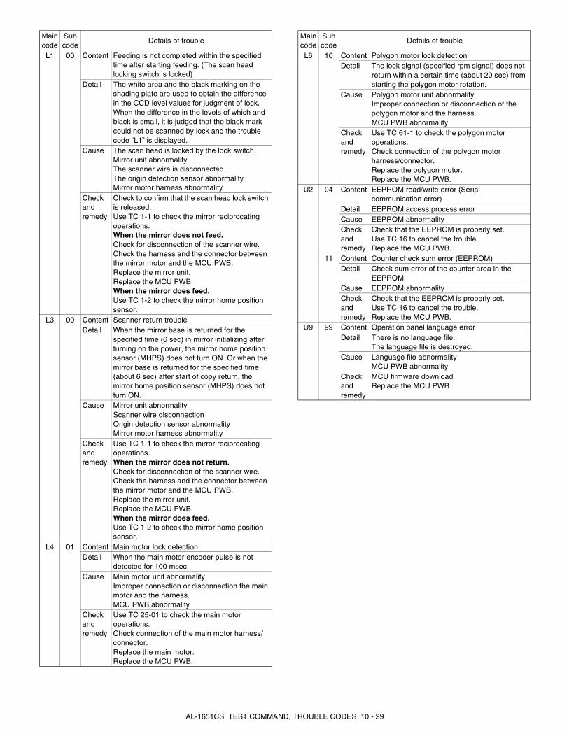
L1 00 Content Feeding is not completed within the specified time after starting feeding. (The scan head locking switch is locked)
Detail The white area and the black marking on the shading plate are used to obtain the difference in the CCD level values for judgment of lock. When the difference in the levels of which and black is small, it is judged that the black mark could not be scanned by lock and the trouble code “L1” is displayed.
Cause The scan head is locked by the lock switch.Mirror unit abnormalityThe scanner wire is disconnected.The origin detection sensor abnormalityMirror motor harness abnormality
Check and remedy
Check to confirm that the scan head lock switch is released.Use TC 1-1 to check the mirror reciprocating operations.When the mirror does not feed.Check for disconnection of the scanner wire.Check the harness and the connector between the mirror motor and the MCU PWB.Replace the mirror unit.Replace the MCU PWB.When the mirror does feed.Use TC 1-2 to check the mirror home position sensor.
L3 00 Content Scanner return troubleDetail When the mirror base is returned for the
specified time (6 sec) in mirror initializing after turning on the power, the mirror home position sensor (MHPS) does not turn ON. Or when the mirror base is returned for the specified time (about 6 sec) after start of copy return, the mirror home position sensor (MHPS) does not turn ON.
Cause Mirror unit abnormalityScanner wire disconnectionOrigin detection sensor abnormalityMirror motor harness abnormality
Check and remedy
Use TC 1-1 to check the mirror reciprocating operations.When the mirror does not return.Check for disconnection of the scanner wire.Check the harness and the connector between the mirror motor and the MCU PWB.Replace the mirror unit.Replace the MCU PWB.When the mirror does feed.Use TC 1-2 to check the mirror home position sensor.
L4 01 Content Main motor lock detectionDetail When the main motor encoder pulse is not
detected for 100 msec.Cause Main motor unit abnormality
Improper connection or disconnection the main motor and the harness.MCU PWB abnormality
Check and remedy
Use TC 25-01 to check the main motor operations.Check connection of the main motor harness/connector.Replace the main motor.Replace the MCU PWB.
Main code
Sub code
Details of trouble
L6 10 Content Polygon motor lock detectionDetail The lock signal (specified rpm signal) does not
return within a certain time (about 20 sec) from starting the polygon motor rotation.
Cause Polygon motor unit abnormalityImproper connection or disconnection of the polygon motor and the harness.MCU PWB abnormality
Check and remedy
Use TC 61-1 to check the polygon motor operations.Check connection of the polygon motor harness/connector.Replace the polygon motor.Replace the MCU PWB.
U2 04 Content EEPROM read/write error (Serial communication error)
Detail EEPROM access process errorCause EEPROM abnormalityCheck and remedy
Check that the EEPROM is properly set.Use TC 16 to cancel the trouble.Replace the MCU PWB.
11 Content Counter check sum error (EEPROM)Detail Check sum error of the counter area in the
EEPROMCause EEPROM abnormalityCheck and remedy
Check that the EEPROM is properly set.Use TC 16 to cancel the trouble.Replace the MCU PWB.
U9 99 Content Operation panel language errorDetail There is no language file.
The language file is destroyed. Cause Language file abnormality
MCU PWB abnormalityCheck and remedy
MCU firmware downloadReplace the MCU PWB.
Main code
Sub code
Details of trouble
AL-1651CS TEST COMMAND, TROUBLE CODES 10 - 29

[11] USER PROGRAM
The user settings consist of the following items.
1. User programsA. Copy mode
Programnumber
Program nameSetting codes
(factory default setting appears in bold)
Explanation
1 AUTO CLEAR 1: 10 SEC.2: 30 SEC.3: 60 SEC.4: 90 SEC.5: 120 SEC.6: OFF
• Auto clear time automatically returns the copy settings to the initial settings if no keys are pressed for a preset period of time following the end of a copy job.
• This program is used to select the period of time. Auto clear time can also be disabled.
2 PREHEAT MODE 1: 30 SEC.2: 1 MIN.3: 5 MIN.4: 30 MIN.5: 60 MIN.6: 120 MIN.7: 240 MIN.
• This function automatically switches the machine to a low power consumption state if the set duration of time elapses without the machine being used when the power is on. The power save indicator lights up, however, the keys on the operation panel can be used. Normal operation automatically resumes when a key on the operation panel is pressed, an original is placed, a print job is received.
3 AUTO SHUT-OFF 1: ON2: OFF
• Use this setting to enable or disable auto power shut-off mode.
4 AUTO SHUT-OFF TIME
1: 5 MIN.2: 30 MIN.3: 60 MIN.4: 120 MIN.5: 240 MIN.
• This function automatically switches the machine to a state that consumes even less power than preheat mode if the set duration of time elapses without the machine being used when the power is on. All lights except the power save indicator go off. To resume normal operation, press the [START] key. Normal operation also resumes automatically when a print job is received or scanning is begun from a computer. While in auto power shut-off mode, no keys (except the [START] key) can be used.
5 STREAM FEEDING 1: ON2: OFF
• When copying using the RSPF, while "SET ORIGINALS FOR STREAM FEEDING." appears in the display after an original has been scanned (about 5 seconds), a subsequent original can be placed and automatically fed into the machine.
6 LAYOUT IN 2IN1 1: PATTERN 12: PATTERN 2
• Use this setting to select the layout pattern when two original pages are copied onto a single sheet of paper (see page 35 for the layout patterns).
7 OFFSET FUNCTION
1: ON2: OFF
• When enabled, this function offsets the position in the paper output tray of sets of copies during sort copy or copy job, and print jobs when using the printer function.
8 ROTATE ORIG. IMAGE
1: ON2: OFF
• When two-sided copying is performed, this function rotates the image on the back of the original. This is convenient when binding the copies at the top (tablet binding).
9 AE/TEXT RESOLUTION
1: 300dpi2: 600dpi
• The copy resolution in auto and text mode is normally 300 dpi. If high-quality copies are preferred, use this setting to change the resolution to 600 dpi.
10 2-SIDED COPY MODE
1: HI-SPEED2: NORMAL
• If the memory fills up when two-sided copying is performed, "NORMAL" can be selected to make copying possible. However, "NORMAL" results in a slower copying speed. Normally "HI-SPEED" is selected to enable fast two-sided copying.
11 MARGIN WIDTH 1: 1/4"2: 1/2"3: 3/4"4: 1"
• Use this setting to set the margin width.
12 MEM. FOR PRINTER
1: 30%2: 40%3: 50%4: 60%5: 70%
• Use this to change the proportion of machine memory used for printer mode.
13 AUTO KEY REPEAT 1: ON2: OFF
• Use this setting to select whether or not holding down a key causes repeated input of the key. For keys that normally cause a set value to increase when held down (for example, holding down the [<] key [v] or [>] key [^]), this program can be used to have the set value not change when the key is held down.
14 KEY PRESS TIME 1: NORMAL2: 0.5 SEC.3: 1.0 SEC.4: 1.5 SEC.5: 2.0 SEC.
• Use this setting to select how long a key must be pressed for the input to be accepted. By selecting a longer time, you can prevent settings from being changed by the accidental pressing of a key.
15 KEY TOUCH SOUND
1: LOW2: HIGH3: OFF
• This sets the volume of beep signals.
AL-1651CS USER PROGRAM 11 - 1

B. Print mode
*1: The scanning speed increases when the USB 2.0 mode is set to "HI-SPEED", however, the printing speed does not increase considerably.
2. Selecting a setting for a user program
1) Press the [MENU] key and then press the [ENTER] key.
In printer mode, the user programs are accessed by simply press-ing the [MENU] key.
2) Press the [<] key [v] or [>] key [^] to select the item that you wishto configure in the USER PROGRAM items, and then press the[ENTER] key.
• You can also select a program by directly entering the programnumber with the numeric keys.
3) Press the [<] key [v] or [>] key [^] to change the setting of theselected item.
NOTE:
• If you mistakenly select the wrong item, press the [CLEAR] key [C]and repeat the procedure from step 2.
• To cancel a setting for a user program, press the [MENU] key.
4) Press the [ENTER] key.
Your selection appears briefly and then the previous screenappears.
NOTE:
When "AE LEVEL ADJUST" is selected in the user programs and the[ENTER] key is pressed, the automatic exposure adjustment screenappears. Adjust the exposure and press the [ENTER] key.
16 SOUND AT DEFAULT
1: ON2: OFF
• Use this to sound a beep when a base setting is selected.
17 TONER SAVE MODE
1: ON2: OFF
• This mode reduces toner usage by about 10% when copying. Toner save mode is effective when the exposure mode is AUTO or TEXT.
18 AE LEVEL ADJUST 1: SPF/RSPF2: DOCUMENT GLASS
• This is used to adjust the exposure level.• The automatic exposure level can be adjusted separately for the document glass
and the RSPF.19 LANGUAGE 1: AMERICAN ENGLISH This is used to set the language used in the display.20 RESET FACTORY 1: Yes
2: NoThis is used to return all settings to the factory default settings.
Programnumber
Program nameSetting codes
(factory default setting appears in bold)
Explanation
Programnumber
Program nameSetting codes
(factory default setting appears in bold)
Explanation
1 FORCED OUTPUT 1: ON2: OFF
When this function is enabled, printing in printer mode will automatically continue using a different size of paper if the specified size of paper runs out in all trays. This feature does not function in copy mode.
2 USB 2.0 MODE SWITCH *1
1: FULL-SPEED2: HI-SPEED
This sets the USB 2.0 data transfer speed. To obtain the fastest speed when using the USB 2.0 port, first verify that your computer meets the system requirements (operating system and driver), and then use this program to change the USB 2.0 mode to "Hi-Speed". Note that the setting should not be changed while running a TWAIN driver. (For the system requirements.)
MAIN MENU1:USER PROGRAM
USER PROGRAM2:PREHEAT MODE
PREHEAT MODE1:30 SEC.
Audible signals (key entry beep, invalid key beep, base setting beep)
The machine sounds three different types of beep signals: a keyentry beep that sounds when a valid key is pressed, an invalid keybeep that sounds when an invalid key is pressed, and a base settingbeep that sounds when a setting is the same as the base setting(base settings are explained below). The base setting beep is initiallydisabled. If you wish to enable the base setting beep, see "SOUNDAT DEFAULT". If you wish to change the volume of the beep signalsor disable them, see "KEY TOUCH SOUND".
The beep patterns of each type of beep signal are as follows:Key entry beep: One beepInvalid key beep: Two beeps
Base setting beep: Three beeps
Base settings
The base settings are preset standard selections for each copy set-ting. The base settings are as follows:Copy ratio: 100%Light and Dark level: center
Paper feed location: Paper trayAUTO/TEXT/PHOTO: AUTO
AL-1651CS USER PROGRAM 11 - 2
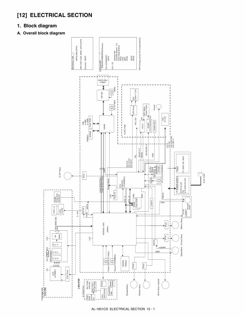
[12] ELECTRICAL SECTION
1. Block diagramA. Overall block diagram
Car
riag
e U
nit
CC
D P
WB
12V
12V
Reg
A5V
3.
3V
R G8b
its(M
SB
/LS
B)
BS
PF
Mot
or5V
Mec
hani
cal L
oad
MP
FS
,RR
S,C
PF
S1
MC
U-P
WB
(SP
F U
NIT
) S
GS
, SR
RC
, SP
US
SP
PS
AL
Mod
el O
nly
4Mb
or 8
Mb
(Cou
nter
)M
CN
T25
6Mbx
1or
16M
b3.
3V
Sen
sor/
SW
(E
lect
roni
c de
tect
or/S
W/S
enso
r)U
AR
T IN
TE
RR
UP
TP
rinte
r C
LK(1
6.15
11M
Hz)
SP
PD
3.3V
I/O
Sca
nner
CLK
(48M
Hz)
16.1
511M
Hz
12M
Hz
Inte
rlock
SW
Cas
sette
det
ecto
rX
2D
rum
Initi
al d
etec
tor
PP
D1
PO
DA
[19…
1]
O
PE
PW
BM
FD
Dup
lex M
otor
PP
D2
D[1
5…0]
SD
OD
1Mbi
tS
PO
DP
SL
LED
Shi
fter
Mot
orN
ote:
Ene
rgy-
savi
ng 1
W c
orre
spon
denc
e)8M
bit
8bit
I2C
Bus
8b
it2K
byte
Buz
zer
Fan
Mot
or (
1spe
ed)
Mai
nMot
orT
oner
Mot
orM
irror
Mot
or
Pol
ygon
Mot
or
AC
Cod
e
KR
ON
OS
AS
IC
(296
pin)
CP
UH
8S/2
321
(19.
6608
MH
z)
LSU
EE
PR
OM
SD
RA
M
16M
byte
Res
et IC
S
RA
M
Driv
er
Fla
sh R
OM
AF
E(A
D98
26)
C D S
A G C
M P XA
D 16
bits
CC
D D
river
CC
FL
x 2
Lam
pIn
vert
er
HO
ME
PO
SIT
ION
SE
NS
OR
CC
D(u
PD
8861
)
CP
U C
LK(1
9.66
08M
Hz)
Sys
tem
Res
et
SS
CG
PMD
Driv
er
LED
Driv
erLE
DC
opie
r 11
pcs
HC
151
KE
Y M
atrix
Cop
ier
24pc
s
ST
AR
T K
EY
P
OW
ER
SU
PP
LY
/PO
FF
,HL,
PR
FW
3.3V
,5V
EN
,5V
,24V
HV
U T
C, G
RID
, MC
, BIA
S
PM
CLK
PS
W
KE
YIN
SE
LIN
1,2,
3
OP
-CLK
OP
-LA
TC
HO
P-D
AT
A
PS
L
MH
PS
Driv
er
Driv
er
/MMRDY
/MMD
PW
M
0 -
24V
HC
151
DC
-DC
Imag
e B
US
(PI-
Bus
)Im
age
BU
S(P
O-B
us)
OA
982
SD
RA
MF
lash
RO
M
8 8
KE
YS
CA
N1-
3
ISP
1581
USB2.0High-speed
LCD
(2 x
20)
HC
238
(3 to
8 d
ecod
e)
EE
PR
OM
(CR
UM
)
LCD
ELC
D R
SLC
D R
/W(T
BD
)LC
D D
B7-
4
Driv
er
LCX
574
LAS
ER
NIC
PC
BA
(Int
erna
l) R
J45
(N/W
conn
ecto
r)E
ther
Chi
pR
TL8
019A
S
FP
GA
CP
UuP
D70
3100
Flas
hRO
M1M
bit
SR
AM
256k
bit
AL-1651CS ELECTRICAL SECTION 12 - 1

2. Circuit descriptionsA. Main PWB (MCU)
(1) GeneralThe MCU PWB is composed of:
• CPU peripheral section which performs mechanical sequencecontrol, U/I, and each function job management.The CPU connects with the ASIC and memory by use of the systembus and performs jog management and sequence control of thewhole engine.
• Image process ASIC which performs image process, CCD control,LSU control, and print control.
• OA982 peripheral section which performs E-Sort and FAX control.(The AL-1651CS has no FAX function.)The OA982 performs image data input/output with the ASIC,SDRAM memory management, and communication with USB2.0devices.
• I/F section for USB2.0 and IEEE1284 control. (For the AL series,IEEE1284 is not available.)
• Motor control circuit
• Mechanical load, sensor I/O circuit
It performs control and management of the process, the transportloads, the fusing, the optical, and the operation panel sections for exe-cuting a series of copy/print/scan operations.
(2) CPU signal table (H8S/2321)
PIN No.
Signal codeInput/Output
Operating
1 /CS1 Output SRAM chip select2 /CS0 Output Flash ROM chip select3 GND DGND4 GND DGND5 Vcc CPU3.3V6 A0 Output Address bus7 A1 Output Address bus8 A2 Output Address bus9 A3 Output Address bus
10 GND DGND11 A4 Output Address bus12 A5 Output Address bus13 A6 Output Address bus14 A7 Output Address bus15 A8 Output Address bus16 A9 Output Address bus17 A10 Output Address bus18 A11 Output Address bus19 GND DGND20 A12 Output Address bus21 A13 Output Address bus22 A14 Output Address bus23 A15 Output Address bus24 A16 Output Address bus25 A17 Output Address bus26 A18 Output Address bus27 A19 Output Address bus28 GND DGND29 A20 Pull-Up30 PSW Interruption
level inputPrint SW
31 SPPD Interruption level input
SPF paper sensor
32 CCD_TG Interruption level input
CCD horizontal sync signal
33 MHPS Interruption level input
Mirror Home Position
34 /CPUSYNC Interruption level input
Horizontal sync (ASIC)
35 GND DGND36 GND DGND
37 FW Interruption level input
Zero cross signal
38 ARB_INT Interruption level input
ASIC interruption
39 Vcc CPU3.3V40 D0 Data I/O Data bus41 D1 Data I/O Data bus42 D2 Data I/O Data bus43 D3 Data I/O Data bus44 GND DGND45 D4 Data I/O Data bus46 D5 Data I/O Data bus47 D6 Data I/O Data bus48 D7 Data I/O Data bus49 D8 Data I/O Data bus50 D9 Data I/O Data bus51 D10 Data I/O Data bus52 D11 Data I/O Data bus53 GND DGND54 D12 Data I/O Data bus55 D13 Data I/O Data bus56 D14 Data I/O Data bus57 D15 Data I/O Data bus58 Vcc CPU3.3V59 POFF Output Shut off control60 TxD1 Output For debug61 SDA Output EEPROM Data bus62 SCL Output EEPROM clock63 LCDRS Output LCD control64 LCDE Output LCD control65 GND DGND66 CS4 (FAX) Chip select (FAX)67 GND DGND68 GND DGND69 RY/BY Input Flash Busy signal70 LCDDB4 Output LCD control71 LCDDB5 Output LCD control72 BZR Output Buzzer signal73 LCDDB7 Output LCD control74 LCDDB6 Output LCD control75 Reset OUT1 Output Reset signal76 DMT0 Output Duplex Motor signal77 DMT1 Output Duplex Motor signal78 DMT2 Output Duplex Motor signal79 DMT3 Output Duplex Motor signal80 WDTOVF Output NC Pull-Up81 /RES Input Reset82 NMI Output NC Pull-Up83 STBY Output NC Pull-Up84 Vcc CPU3.3V85 XTAL Input Clock86 EXTAL Output Clock87 GND DGND88 CPUCLK Output NC89 Vcc CPU3.3V90 PRINTST Output Print start signal91 /RD Output Read signal92 /HWR Output Write signal (High address)93 /LWR Output Write signal (Low address)94 SELIN3 Output HC151 select signal 95 SELIN2 Output HC151 select signal96 SELIN1 Output HC151 select signal97 ESSTS Output E-sort control98 ESCMD Input E-sort control99 GND DGND100 GND DGND101 ESSRDY Input E-sort control102 ESCRDY Output E-sort control103 AVcc CPU3.3V104 Vref CPU3.3V
PIN No.
Signal codeInput/Output
Operating
AL-1651CS ELECTRICAL SECTION 12 - 2

(3) Image process ASIC (HG73C114HF)a. General
The ASIC is composed of the three blocks: the image process block,the print control block, and the I/F block.
Image process section
According to the operation mode set by the register set value, theimage data from the CCD PWB are placed under shading, AE pro-cess, input gamma process, area separation, filter process, resolu-tion conversion, zoom process, output gamma process, and binarycoding.
Print control section
During copying, image-processed data are outputted to the LSU atthe timing of LSU writing.
I/F section
This section performs DRUM control as image data buffer, imagedata send/receive with the OA982, and data send/receive with theIEEE1284 I/F.
105 RTH Analog input
Fusing thermistor
106 ESPAGE Input E-sort control107 SIN1 Input HC151 select detection108 SIN2 Input HC151 select detection109 SIN3 Input HC151 select detection110 Pull up111 KEY IN Input NC112 MSUST1 Input NC113 Avss DGND114 GND DGND115 /SCANSP Output Scan STOP signal116 /SCANST Output Scan START signal117 /TRANSST Output ASIC transfer signal118 PMCLK Output Polygon clock119 SPMT3 Output SPF motor signal120 SPMT2 Output SPF motor signal121 SPMT1 Output SPF motor signal122 SPMT0 Output SPF motor signal123 GND DGND124 GND DGND125 Vcc CPU3.3V126 PSL Output Power save LED control127 /CS3 Output Chip select signal128 /CS2 Output ASIC chip select
PIN No.
Signal codeInput/Output
Operating
nCS2
nRD PORT1OUT[15..0]
nLWR PORT2OUT[10..0]
A[9..1]
D[15..0] OPE-LATCH
LED Driver OPE-DATA to OPU-PWBnRESET Control OPE-CLK
JTAG TONER MOTOR TMCLK,TMEN to TONNER MOTOR DRIVERControl TM,TM-
to SDRAM64Mb or 128Mb CCD-RS,CCD-CK1,CCD-CK2 to CCD(SCAN UNIT)(Op.400MByte) CCD-CP,CCD-SHR
bsmp,vsmp,mclk,OEB
afesen,afesck,afesdito AFE(SCAN UNIT)
to USB I/F
AFE-DB[7..0]
to IEEE1284 I/F
MIRCNT,MTR-Y1,MTR-PH-1,MTR-I01,MTR-I11,MTR-I21
MTR-Y2,MTR-PH-2,MTR-I02,MTR-I12,MTR-I22
to MIRROR MOTOR DRIVERSYNC
to LSU-PWB LD to CCFL(Scan UNIT)LEND CL
CPUSYNC
I/O PORT
CPU BUSI/F
AL-1651CS ELECTRICAL SECTION 12 - 3

d. ASIC (Signal table)
PIN No.
Signal Name IN/OUT Connected to Description
1 cpudata7 IN/OUT CPU CPU data bus2 cpudata6 IN/OUT CPU CPU data bus3 cpudata5 IN/OUT CPU CPU data bus4 cpudata4 IN/OUT CPU CPU data bus5 VCC_AC Power6 cpudata3 IN/OUT CPU CPU data bus7 cpudata2 IN/OUT CPU CPU data bus8 cpudata1 IN/OUT CPU CPU data bus9 cpudata0 IN/OUT CPU CPU data bus10 GND_AC Power11 mircnt OUT Buffer IC SPF scanner select
signal 12 cpusync OUT CPU CPU SYNC signal13 mem_intr Not used14 arb_intr OUT CPU INTR signal15 VCC_core Power16 cpu_ad8 IN CPU CPU address bus17 cpu_ad7 IN CPU CPU address bus18 cpu_ad6 IN CPU CPU address bus19 cpu_ad5 IN CPU CPU address bus20 GND_core Power21 ram_clk_in IN ASIC SDRAM clock on the
board22 cpu_ad4 IN CPU CPU address bus23 cpu_ad3 IN CPU CPU address bus24 cpu_ad2 IN CPU CPU address bus25 cpu_ad1 IN CPU CPU address bus26 cpu_ad0 IN CPU CPU address bus27 xcpucs IN CPU CS signal28 sfclk IN Oscillator Clock29 GND_core Power30 xcpuwr IN CPU CPU write signal31 xcpurd IN CPU CPU read signal32 nrst IN SYSTEM
RESETSYSTEM RESET
33 VCC_core Power34 pfclk2 IN Not used35 clock_sw IN Pull up36 GND_core Power37 pfclk1_xout OUT X-tal units VIDEO clock38 pfclk1 IN X-tal units VIDEO clock39 VSSPLL2 Pull up40 VDDPLL2 Pull up41 VSS2 Pull up42 VDDI2 Pull up43 tm2_15m Pull up44 xsync IN LSU Horizontal sync
signal from LSU (/SYNC)
45 GND_AC Power46 xld OUT LSU Laser drive signal 47 xlend OUT LSU Laser APC signal 48 VCC_AC Power49 mmd OUT Tr array IC Main motor control
signal. "H": Main motor ON
50 pmd OUT I/O Polygon motor drive51 tc OUT Tr array IC Transfer charger
control signal. "H":ON52 gridl OUT Tr array IC Main charger grid
control signal. "H": L output
53 mc OUT Tr array IC Main charger control signal. "H": ON
54 bias OUT I/O HV bias drive55 NC OUT I/O Not used56 vfmcnt OUT Tr array IC Ventilation fan
rotation speed control signal. "H": High speed, "L": Low speed
57 VCC_core Power58 vfm OUT Tr array IC Ventilation fan control
signal. "H": Fan ON59 /FPOFF OUT I/O FAX poff signal60 GND_core Power61 DEV DIR OUT I/O CRUM bus control62 spfclh OUT Tr array IC SPF/RSPF resist
roller clutch control signal "H":ON
63 spfrsol OUT Tr array IC SPF/RSPF document feed solenoid control signal "H":ON
64 spfgsol OUT Tr array IC SPF/RSPF gate solenoid control signal "H":ON
65 spfpsol OUT Tr array IC SPF/RSPF document transport solenoid control signal "H":ON
66 VCC_core Power67 bias OUT Tr array IC DV bias control
signal. "H":ON68 lden OUT Tr array IC Laser circuit control
signal. "H": Laser circuit ON
69 GND_AC Power70 MRPS1 OUT I/O SPF current control71 MRPS2 OUT I/O SPF current control72 MRPS3 OUT I/O SPF current control73 CPFS1 OUT I/O 1st cassette pick up
solenoid74 VCC_AC Power75 CPFS2 OUT I/O 2nd cassette pick up
solenoid76 pr OUT I/O Power relay control77 hl OUT Tr array IC Heater lamp control
signal. "H":ON78 GND_core Power79 MPFS OUT I/O Multi-bypass solenoid80 miron OUT Buffer IC SPF scanner select
signal 81 spfon OUT Buffer IC SPF ON signal82 KEYSC1 OUT I/O Key sense control83 KEYSC2 OUT I/O Key sense control84 KEYSC3 OUT I/O Key sense control85 IMC ready OUT I/O IMC control86 VCC_core Power87 tmx OUT Buffer IC Toner motor control
signal 88 tm OUT Buffer IC Toner motor control
signal 89 op_data OUT Tr array IC Operation circuit data
signal90 ope_latch OUT Tr array IC Operation circuit latch
signal. Data take-in at "L"
91 GND_AC Power
PIN No.
Signal Name IN/OUT Connected to Description
AL-1651CS ELECTRICAL SECTION 12 - 4
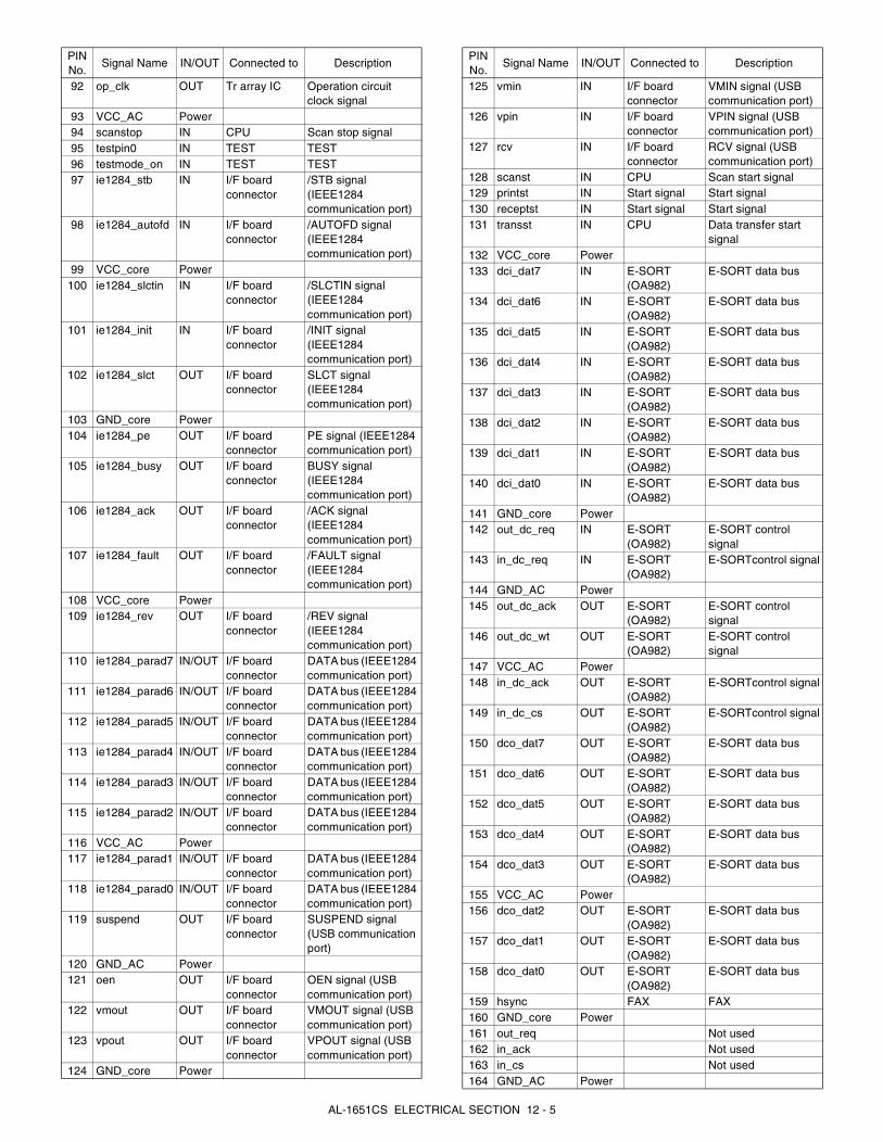
92 op_clk OUT Tr array IC Operation circuit clock signal
93 VCC_AC Power94 scanstop IN CPU Scan stop signal95 testpin0 IN TEST TEST96 testmode_on IN TEST TEST97 ie1284_stb IN I/F board
connector/STB signal (IEEE1284 communication port)
98 ie1284_autofd IN I/F board connector
/AUTOFD signal (IEEE1284 communication port)
99 VCC_core Power100 ie1284_slctin IN I/F board
connector/SLCTIN signal (IEEE1284 communication port)
101 ie1284_init IN I/F board connector
/INIT signal (IEEE1284 communication port)
102 ie1284_slct OUT I/F board connector
SLCT signal (IEEE1284 communication port)
103 GND_core Power104 ie1284_pe OUT I/F board
connectorPE signal (IEEE1284 communication port)
105 ie1284_busy OUT I/F board connector
BUSY signal (IEEE1284 communication port)
106 ie1284_ack OUT I/F board connector
/ACK signal (IEEE1284 communication port)
107 ie1284_fault OUT I/F board connector
/FAULT signal (IEEE1284 communication port)
108 VCC_core Power109 ie1284_rev OUT I/F board
connector/REV signal (IEEE1284 communication port)
110 ie1284_parad7 IN/OUT I/F board connector
DATA bus (IEEE1284 communication port)
111 ie1284_parad6 IN/OUT I/F board connector
DATA bus (IEEE1284 communication port)
112 ie1284_parad5 IN/OUT I/F board connector
DATA bus (IEEE1284 communication port)
113 ie1284_parad4 IN/OUT I/F board connector
DATA bus (IEEE1284 communication port)
114 ie1284_parad3 IN/OUT I/F board connector
DATA bus (IEEE1284 communication port)
115 ie1284_parad2 IN/OUT I/F board connector
DATA bus (IEEE1284 communication port)
116 VCC_AC Power117 ie1284_parad1 IN/OUT I/F board
connectorDATA bus (IEEE1284 communication port)
118 ie1284_parad0 IN/OUT I/F board connector
DATA bus (IEEE1284 communication port)
119 suspend OUT I/F board connector
SUSPEND signal (USB communication port)
120 GND_AC Power121 oen OUT I/F board
connectorOEN signal (USB communication port)
122 vmout OUT I/F board connector
VMOUT signal (USB communication port)
123 vpout OUT I/F board connector
VPOUT signal (USB communication port)
124 GND_core Power
PIN No.
Signal Name IN/OUT Connected to Description
125 vmin IN I/F board connector
VMIN signal (USB communication port)
126 vpin IN I/F board connector
VPIN signal (USB communication port)
127 rcv IN I/F board connector
RCV signal (USB communication port)
128 scanst IN CPU Scan start signal129 printst IN Start signal Start signal130 receptst IN Start signal Start signal131 transst IN CPU Data transfer start
signal132 VCC_core Power133 dci_dat7 IN E-SORT
(OA982)E-SORT data bus
134 dci_dat6 IN E-SORT (OA982)
E-SORT data bus
135 dci_dat5 IN E-SORT (OA982)
E-SORT data bus
136 dci_dat4 IN E-SORT (OA982)
E-SORT data bus
137 dci_dat3 IN E-SORT (OA982)
E-SORT data bus
138 dci_dat2 IN E-SORT (OA982)
E-SORT data bus
139 dci_dat1 IN E-SORT (OA982)
E-SORT data bus
140 dci_dat0 IN E-SORT (OA982)
E-SORT data bus
141 GND_core Power142 out_dc_req IN E-SORT
(OA982)E-SORT control signal
143 in_dc_req IN E-SORT (OA982)
E-SORTcontrol signal
144 GND_AC Power145 out_dc_ack OUT E-SORT
(OA982)E-SORT control signal
146 out_dc_wt OUT E-SORT (OA982)
E-SORT control signal
147 VCC_AC Power148 in_dc_ack OUT E-SORT
(OA982)E-SORTcontrol signal
149 in_dc_cs OUT E-SORT (OA982)
E-SORTcontrol signal
150 dco_dat7 OUT E-SORT (OA982)
E-SORT data bus
151 dco_dat6 OUT E-SORT (OA982)
E-SORT data bus
152 dco_dat5 OUT E-SORT (OA982)
E-SORT data bus
153 dco_dat4 OUT E-SORT (OA982)
E-SORT data bus
154 dco_dat3 OUT E-SORT (OA982)
E-SORT data bus
155 VCC_AC Power156 dco_dat2 OUT E-SORT
(OA982)E-SORT data bus
157 dco_dat1 OUT E-SORT (OA982)
E-SORT data bus
158 dco_dat0 OUT E-SORT (OA982)
E-SORT data bus
159 hsync FAX FAX160 GND_core Power161 out_req Not used162 in_ack Not used163 in_cs Not used164 GND_AC Power
PIN No.
Signal Name IN/OUT Connected to Description
AL-1651CS ELECTRICAL SECTION 12 - 5

165 mdat00 Not used166 mdat01 Not used167 mdat02 Not used168 mdat03 Not used169 VCC_core Power170 mdat04 Not used171 mdat05 Not used172 mdat06 Not used173 GND_core Power174 mdat07 Not used175 mdat08 Not used176 mdat09 Not used177 VCC_AC Power178 mdat10 Not used179 mdat11 Not used180 mdat12 Not used181 VCC_core Power182 mdat13 Not used183 mdat14 Not used184 mdat15 Not used185 GND_AC Power186 pcl_s_print Not used187 fax_s_print Not used188 es_s_print Not used189 out_ack Not used190 out_cs Not used191 in_req Not used192 VCC_core Power193 TCK JTAG Not used194 TMS JTAG Not used195 TRSTA JTAG Not used196 TDI JTAG Not used197 TDO JTAG Not used198 GND_core Power199 afp_vsmp OUT CCD PWB AFE control signal200 ccd_tg OUT CCD PWB CCD control signal201 ccdrs OUT CCD PWB CCD control signal202 afp_bsmp OUT CCD PWB AFE control signal203 ccdcp OUT CCD PWB CCD control signal204 afe_sdata IN CCD PWB AD's serial data205 ccd_ph2 OUT CCD PWB CCD control signal206 ccd_ph1 OUT CCD PWB CCD control signal207 afp_afesen OUT CCD PWB AFE control signal208 GND_core Power209 afp_adcclk OUT CCD PWB AFE control signal210 VCC_core Power211 afp_afesck OUT CCD PWB AFE control signal212 GND_AC Power213 afp_data7 IN CCD PWB Image scan data214 afp_data6 IN CCD PWB Image scan data215 afp_data5 IN CCD PWB Image scan data216 afp_data4 IN CCD PWB Image scan data217 afp_data3 IN CCD PWB Image scan data218 afp_data2 IN CCD PWB Image scan data219 afp_data1 IN CCD PWB Image scan data220 afp_data0 IN CCD PWB Image scan data221 VCC_AC Power222 cl OUT Logic IC Copy lamp control
signal223 GND_core Power224 mtr_y3 OUT I/O Carriage motor
current control signal 225 mtr_y2 OUT Tr array IC Carriage motor
current control signal
PIN No.
Signal Name IN/OUT Connected to Description
226 mtr_y1 OUT Tr array IC Carriage motor current control signal
227 VCC_core Power228 mtr_phase2 OUT Motor driver Carriage motor
control signal 229 mtr_i02 OUT Motor driver Carriage motor
control signal 230 mtr_i12 OUT Motor driver Carriage motor
control signal 231 mtr_i22 OUT Motor driver Carriage motor
control signal 232 mtr_phase1 OUT Motor driver Carriage motor
control signal 233 mtr_i01 OUT Motor driver Carriage motor
control signal 234 mtr_i11 OUT Motor driver Carriage motor
control signal 235 mtr_i21 OUT Motor driver Carriage motor
control signal 236 GND_AC Power237 ram_mad3 OUT SDRAM SDRAM (Image
process page memory) address bus
238 ram_mad2 OUT SDRAM SDRAM (Image process page memory) address bus
239 GND_core Power240 ram_mad1 OUT SDRAM SDRAM (Image
process page memory) address bus
241 ram_mad0 OUT SDRAM SDRAM (Image process page memory) address bus
242 ram_mad10 OUT SDRAM SDRAM (Image process page memory) address bus
243 VCC_core Power244 ram_banks1 OUT SDRAM SDRAM (Image
process page memory) BANK signal
245 ram_banks0 OUT SDRAM SDRAM (Image process page memory) BANK signal
246 xram_cs OUT SDRAM (Image process page memory) CS signal
247 xram_ras OUT SDRAM SDRAM (Image process page memory) RAS signal
248 xram_cas OUT SDRAM SDRAM (Image process page memory) CAS signal
249 VCC_AC Power250 xram_wde OUT SDRAM SDRAM (Image
process page memory) WDE signal
251 ram_dqm0 OUT SDRAM SDRAM (Image process page memory) DQM signal
252 GND_AC Power253 ram_data7 IN/OUT SDRAM SDRAM (Image
process page memory) data bus
PIN No.
Signal Name IN/OUT Connected to Description
AL-1651CS ELECTRICAL SECTION 12 - 6
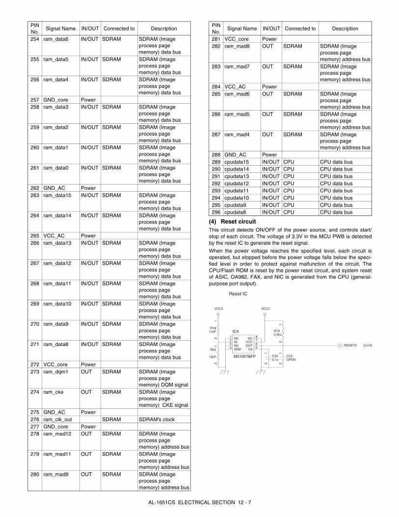
(4) Reset circuitThis circuit detects ON/OFF of the power source, and controls start/stop of each circuit. The voltage of 3.3V in the MCU PWB is detectedby the reset IC to generate the reset signal.
When the power voltage reaches the specified level, each circuit isoperated, but stopped before the power voltage falls below the speci-fied level in order to protect against malfunction of the circuit. TheCPU/Flash ROM is reset by the power reset circuit, and system resetof ASIC, OA982, FAX, and NIC is generated from the CPU (general-purpose port output).
254 ram_data6 IN/OUT SDRAM SDRAM (Image process page memory) data bus
255 ram_data5 IN/OUT SDRAM SDRAM (Image process page memory) data bus
256 ram_data4 IN/OUT SDRAM SDRAM (Image process page memory) data bus
257 GND_core Power258 ram_data3 IN/OUT SDRAM SDRAM (Image
process page memory) data bus
259 ram_data2 IN/OUT SDRAM SDRAM (Image process page memory) data bus
260 ram_data1 IN/OUT SDRAM SDRAM (Image process page memory) data bus
261 ram_data0 IN/OUT SDRAM SDRAM (Image process page memory) data bus
262 GND_AC Power263 ram_data15 IN/OUT SDRAM SDRAM (Image
process page memory) data bus
264 ram_data14 IN/OUT SDRAM SDRAM (Image process page memory) data bus
265 VCC_AC Power266 ram_data13 IN/OUT SDRAM SDRAM (Image
process page memory) data bus
267 ram_data12 IN/OUT SDRAM SDRAM (Image process page memory) data bus
268 ram_data11 IN/OUT SDRAM SDRAM (Image process page memory) data bus
269 ram_data10 IN/OUT SDRAM SDRAM (Image process page memory) data bus
270 ram_data9 IN/OUT SDRAM SDRAM (Image process page memory) data bus
271 ram_data8 IN/OUT SDRAM SDRAM (Image process page memory) data bus
272 VCC_core Power273 ram_dqm1 OUT SDRAM SDRAM (Image
process page memory) DQM signal
274 ram_cke OUT SDRAM SDRAM (Image process page memory) CKE signal
275 GND_AC Power276 ram_clk_out SDRAM SDRAM's clock277 GND_core Power278 ram_mad12 OUT SDRAM SDRAM (Image
process page memory) address bus
279 ram_mad11 OUT SDRAM SDRAM (Image process page memory) address bus
280 ram_mad9 OUT SDRAM SDRAM (Image process page memory) address bus
PIN No.
Signal Name IN/OUT Connected to Description
281 VCC_core Power282 ram_mad8 OUT SDRAM SDRAM (Image
process page memory) address bus
283 ram_mad7 OUT SDRAM SDRAM (Image process page memory) address bus
284 VCC_AC Power285 ram_mad6 OUT SDRAM SDRAM (Image
process page memory) address bus
286 ram_mad5 OUT SDRAM SDRAM (Image process page memory) address bus
287 ram_mad4 OUT SDRAM SDRAM (Image process page memory) address bus
288 GND_AC Power289 cpudata15 IN/OUT CPU CPU data bus290 cpudata14 IN/OUT CPU CPU data bus291 cpudata13 IN/OUT CPU CPU data bus292 cpudata12 IN/OUT CPU CPU data bus293 cpudata11 IN/OUT CPU CPU data bus294 cpudata10 IN/OUT CPU CPU data bus295 cpudata9 IN/OUT CPU CPU data bus296 cpudata8 IN/OUT CPU CPU data bus
PIN No.
Signal Name IN/OUT Connected to Description
R1811kF
21
C220.1u
12
C23OPEN
12
R20
10kF
21
IC4
M51957BFP
NC 8
GND4
VCC 7NC1
IN2
NC3
Cd 5OUT 6
R193.3kJ
21
VCC3 VCC3
/RESET0 (2-C4)
Reset IC
AL-1651CS ELECTRICAL SECTION 12 - 7
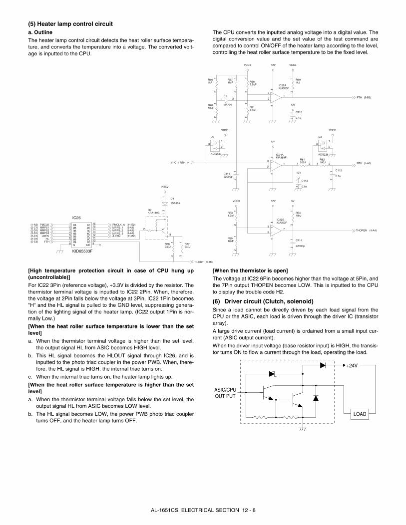
(5) Heater lamp control circuita. Outline
The heater lamp control circuit detects the heat roller surface tempera-ture, and converts the temperature into a voltage. The converted volt-age is inputted to the CPU.
The CPU converts the inputted analog voltage into a digital value. Thedigital conversion value and the set value of the test command arecompared to control ON/OFF of the heater lamp according to the level,controlling the heat roller surface temperature to be the fixed level.
[High temperature protection circuit in case of CPU hung up(uncontrollable)]
For IC22 3Pin (reference voltage), +3.3V is divided by the resistor. Thethermistor terminal voltage is inputted to IC22 2Pin. When, therefore,the voltage at 2Pin falls below the voltage at 3Pin, IC22 1Pin becomes"H" and the HL signal is pulled to the GND level, suppressing genera-tion of the lighting signal of the heater lamp. (IC22 output 1Pin is nor-mally Low.)
[When the heat roller surface temperature is lower than the setlevel]
a. When the thermistor terminal voltage is higher than the set level,the output signal HL from ASIC becomes HIGH level.
b. This HL signal becomes the HLOUT signal through IC26, and isinputted to the photo triac coupler in the power PWB. When, there-fore, the HL signal is HIGH, the internal triac turns on.
c. When the internal triac turns on, the heater lamp lights up.
[When the heat roller surface temperature is higher than the setlevel]
a. When the thermistor terminal voltage falls below the set level, theoutput signal HL from ASIC becomes LOW level.
b. The HL signal becomes LOW, the power PWB photo triac couplerturns OFF, and the heater lamp turns OFF.
[When the thermistor is open]
The voltage at IC22 6Pin becomes higher than the voltage at 5Pin, andthe 7Pin output THOPEN becomes LOW. This is inputted to the CPUto display the trouble code H2.
(6) Driver circuit (Clutch, solenoid)Since a load cannot be directly driven by each load signal from theCPU or the ASIC, each load is driven through the driver IC (transistorarray).
A large drive current (load current) is ordained from a small input cur-rent (ASIC output current).
When the driver input voltage (base resistor input) is HIGH, the transis-tor turns ON to flow a current through the load, operating the load.
R687.5kF
21
R714.3kF
21
D1
MA700
1 2
R671MF
21
R661kF
21
R7010kF
21
R691kJ
21
C11122000p
12 C113
0.1u
12
R81300J 21
R82100J 21
C112
0.1u
12
R831.2kF
21
R8510kF
21
R8410kJ
21
C114
22000p
12
D4
1SS355
12
R86240J
21
R87240J
21
IC22AKIA393F
3
21
84
+
-
C110
0.1u
12
IC22BKIA393F
5
67
84
+
-
IC24AKIA358F
3
21
84
+
-
IC26
KID65503F
1B1
2B2
3B3
4B4
5B5
6B6
7B7
G8 NC 9
1C 16
2C 15
3C14
4C 13
5C 12
6C11
7C10
Q2KRA119S 1
2
3
D2
KDS226
2
13
D3
KDS226
2
13
INT5V
12VVCC3
VCC3 VCC3
12VVCC3
12V
12V
12V
VCC3
5V
MRPS1
HLLDEN
PMCLK
FTH
HLOUT
PMCLK_AMRPS_1
/LDEN
MRPS_2
FTH
RTH
THOPEN
RTH_IN
MRPS2MRPS3 MRPS_3
(11-B2)
(11-B2)
(6-A1)(6-A1)(6-A1)
(5-E3)(2-D1)(2-C1)(2-D1)(2-D1)(2-C1)(1-A2)
(10-B3)
(1-A3)
(4-A4)
(5-B2)
(11-C1)
LOAD
+24V
ASIC/CPUOUT PUT
LOAD
AL-1651CS ELECTRICAL SECTION 12 - 8
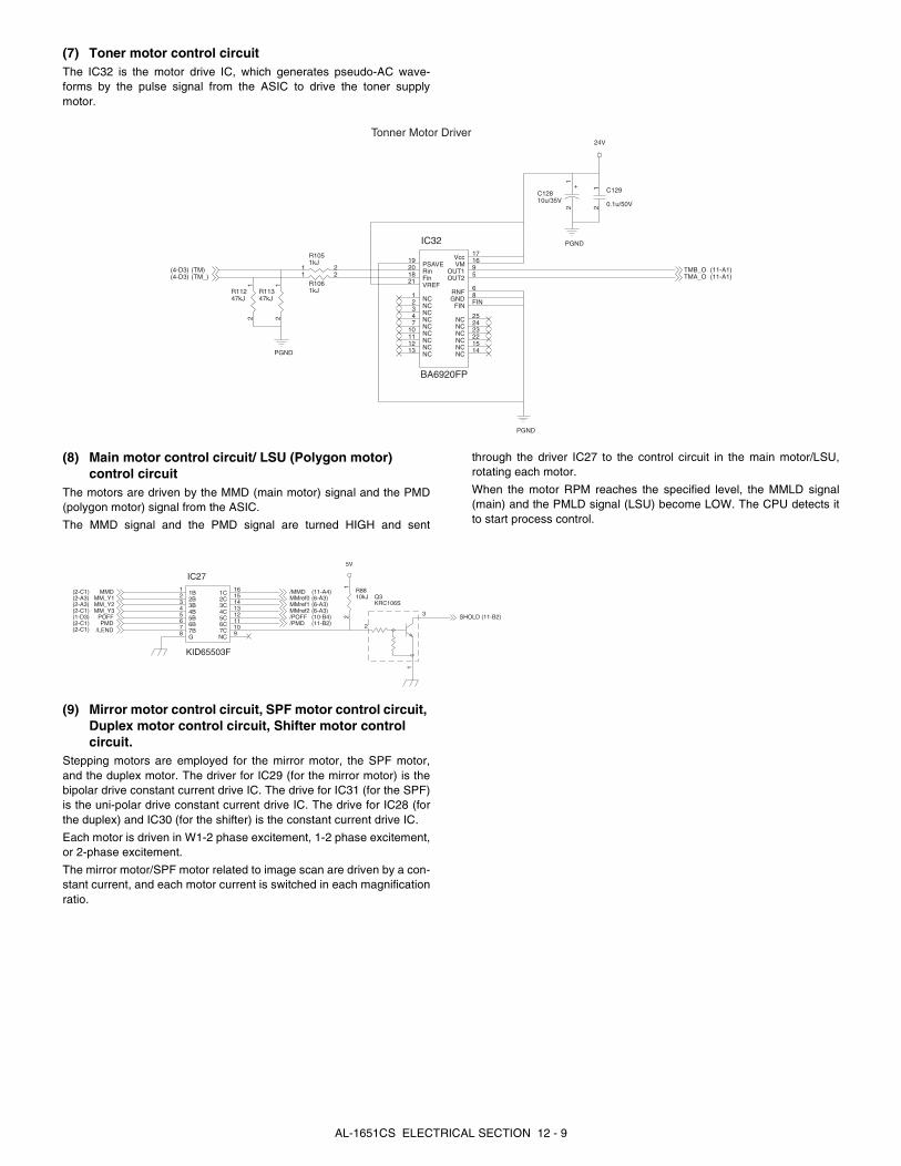
(7) Toner motor control circuitThe IC32 is the motor drive IC, which generates pseudo-AC wave-forms by the pulse signal from the ASIC to drive the toner supplymotor.
(8) Main motor control circuit/ LSU (Polygon motor) control circuit
The motors are driven by the MMD (main motor) signal and the PMD(polygon motor) signal from the ASIC.
The MMD signal and the PMD signal are turned HIGH and sent
through the driver IC27 to the control circuit in the main motor/LSU,rotating each motor.
When the motor RPM reaches the specified level, the MMLD signal(main) and the PMLD signal (LSU) become LOW. The CPU detects itto start process control.
(9) Mirror motor control circuit, SPF motor control circuit, Duplex motor control circuit, Shifter motor control circuit.
Stepping motors are employed for the mirror motor, the SPF motor,and the duplex motor. The driver for IC29 (for the mirror motor) is thebipolar drive constant current drive IC. The drive for IC31 (for the SPF)is the uni-polar drive constant current drive IC. The drive for IC28 (forthe duplex) and IC30 (for the shifter) is the constant current drive IC.
Each motor is driven in W1-2 phase excitement, 1-2 phase excitement,or 2-phase excitement.
The mirror motor/SPF motor related to image scan are driven by a con-stant current, and each motor current is switched in each magnificationratio.
R11347kJ
21
R11247kJ
21
C12810u/35V
12
+
R1051kJ
21
R1061kJ
21
IC32
BA6920FP
Vcc 17
GND 8
Rin20
Fin18 OUT1 9
OUT2 5
VM16
VREF21
RNF6
PSAVE19
NC1
NC2
NC3
NC4
NC7
NC10
NC11
NC12
NC13 NC 14NC 15NC22NC 23NC 24NC 25
FIN FIN
C129
0.1u/50V
12
24V
PGND
PGND
PGND
(TM)(TM_)
TMB_OTMA_O
(4-D3)(4-D3)
(11-A1)(11-A1)
Tonner Motor Driver
IC27
KID65503F
1B1
2B2
3B3
4B4
5B5
6B6
7B7
G8
NC9
1C 16
2C 15
3C 14
4C13
5C 12
6C 11
7C 10
Q3KRC106S
1
2
3
R8810kJ
21
5V
PMD
MM_Y2
MMDMM_Y1
MM_Y3
/PMD
MMref1
/MMD
MMref2
MMref0
POFF /POFF
/LEND
SHOLD(10-B4)(11-B2)
(11-B2)
(11-A4)
(6-A3)(6-A3)(6-A3)
(2-C1)
(2-C1)
(2-C1)
(2-A3)
(2-C1)
(2-A3)
(1-D3)
AL-1651CS ELECTRICAL SECTION 12 - 9
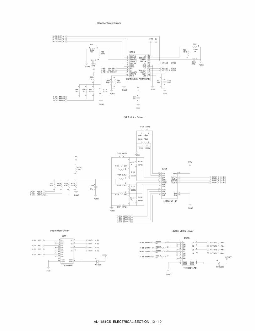
C116820p
1 2
C117820p
12
C118820p
12
C1210.1u
12
C115820p
1 2
C1190.1u
12
R921.5kJ
21
R90
0.68J1W
21
R9430kJ
21
R9530kJ
21
R911.5kJ
21
R89
0.68J1W
21
R98510J
21
R971kJ
21
R962kJ
21
R931kJ
21
IC29
L6219DS or AMM56219
OUT 2A2
SENSE 23
COMP 24
OUT 2B5
GND6
GND7
I028
I129
PHASE 210
VREF 211
RC 212 VSS 13RC 1 14VREF 1 15PHASE 116I11 17GND 18GND 19I0120OUT 1B 21COMP 1 22SENSE 123VS24
OUT 1A1
5V
24VM 5V
5V
PGNDPGND
PGND
PGND
PGND PGND
PGND
PGND
MM_PH_A
OUT_A-
MM_AI0
MM_PH_B
MM_BI0MM_BI1
MM_AI1
OUT_A+
OUT_B-
MMref0MMref1MMref2
OUT_B+
(10-D2)
(2-A3)(2-A3)(2-A3)
(2-A3)
(2-A3)(2-A3)
(5-C1)(5-C1)(5-C1)
Scanner Motor Driver
(10-D2)(10-D2)(10-D2)
R107300J
21
C125 2200p
1 2
R99 7.5kJ21
C126 2200p1 2
R100 7.5kJ
21
C132
2200p
12
C136
OPEN
12
C130
OPEN
12
C127 OPEN
1 2
C137 OPEN1 2
C135
2200p
12
R104 2.4kJ
21
R111 2.4kJ21
R1011kJ
21
R1151kJ
21
C134
0.1u
12
R108620J
21
R1091.2kJ
21
R110100J
21
R102750J
21
R103 1J 2W
21 IC31
MTD1361/F
CrA23
CrB20
VsA25
RsA3
VrefA24
VrefB19
RsB12
VsB18
In /A26
In A27
In /B17
In B16
Vmm 22
OUT /A1
OUT A 4
OUT /B 14
OUT B11
PG 15
PG 28R114 1J 2W21
PGND
PGND
PGND
PGND
PGND
24VM
5V
SPMT_2
(SPFMT2)
SPMT_0SPMT_3SPMT_1
MRPS_1MRPS_2MRPS_3
(SPFMT0)(SPFMT3)(SPFMT1)
(5-C2)(5-C2)(5-C2)
(4-D3)(4-D3)(4-D3)(4-D3)
(11-D1)(11-D1)
(11-E1)
(11-E1)
SPF Motor Driver
D5
MTZ J22B
IC28
TD62064AF
I13
NC4
NC5
I26
NC10
I311
NC12
NC13
GND17
O12
O27
O39
O416
COM1
COM8
GND18
I414
NC15
PGND
24VDup
DMT0 /DMT0
DMT1
DMT2
DMT3
/DMT1
/DMT2
/DMT3
(11-B3)
(11-B3)
(11-B3)
(11-B3)
(1-D3)
(1-D3)
(1-D3)
(1-D3)
Duplex Motor Driver
D6
MTZ J22B
IC30
TD62064AF
I13
NC4
NC5
I26
NC10
I311
NC12
NC13
GND17
O12
O2 7
O39
O4 16
COM1
COM8
GND18
I414
NC15
R3380J
21
R3390J
21
R3400J
21
R3410J
21
PGND
24VSFT
SFTMT0 /SFTMT0
SFTMT1
SFTMT2
/SFTMT1
/SFTMT2
/SFTMT3
SFTMT3
Shifter Motor Driver
(4-B2)
(4-B2)
(4-B2)
(4-B2)
(11-A1)
(11-A1)
(11-A1)
(11-A1)
AL-1651CS ELECTRICAL SECTION 12 - 10

(10) NIC PWBThe NIC PWB is used to realize 10Base-T network functions (printonly). It is provided with the CPU, the Ether chip, FPGA, memory, andthe RJ45LAN connector. Data are converted into IEEE1284 paralleldata and sent to the MCU PWB, realizing network functions.
(11) OPE PWBa. Outline
The operation circuit is composed of the LCD control circuit, the keymatrix circuit, the display matrix circuit, and the buzzer circuit, realizingthe U/I functions.
b. LCD control circuit
The character LCD (COG) in 2 lines and 16 digits is used. The displaydata are sent from the MCU (CPU) to LCD internal registers, control-ling the LCD.
c. Key matrix circuit
The SEL signal is sent from the CPU of MCU to the matrix selector IC(multiplexer) in the operation circuit. The signal detects OFF/ON of thekey, and is sent to the CPU as serial data.
d. LED matrix circuit
The display is controlled by inputting the serial data signal, the clocksignal, and the latch signal from ASIC to the LED driver in the opera-tion circuit.
In the LED driver, data are set to the register (8bit) and latched to con-trol the IC output port, performing matrix-driving of ON/OFF of the LED.
(12) Carriage Unita. Outline
The carriage unit is provided with the CCD PWB, the inverter PWB, thelamps, etc. A document is radiated, and image data read by the CCDare A/D converted to be sent to the ASIC.
b. CCD PWB
The color image sensor uPD8861 (5400 pixels x 3 lines) is used as theCCD on the CCD PWB to scan images in the resolution of 600dpi/USletter size in the main scanning direction.
Image data scanned by the CCD are inputted to AFE (AD9826), wherethey are A/D-converted to output digital data. The output digital dataare sent to the MCU PWB and to the ASIC. The ASIC performs imageprocess with the digital data.
c. Lamp inverter PWB
The transformer is controlled by the lamp control signal from the MCUPWB to turn ON/OFF the cool cathode ray tube by the transformer out-put.
B. DC power circuitThe DC power circuit directly rectifies the AC power and performsswitching-conversion with the DC/DC converter circuit, and rectifiesand smoothes again to generate a DC voltage.
The constant voltage control circuit is of +5VEN. +24V and +12V are ofthe non-control system by winding from the +5VEN winding. As shownin fig (1), +24V, +12V, and +5V are provided with the ON/OFF functionby external signals. +3.3V is outputted from +5VEN to the regulator IC.
Refer to the block diagram, fig (1).
fig (1) Block diagram
(1) Noise filter circuitThe filter circuit is composed of L and C. It reduces common noisesand normal mode noises generated from the AC line.
The common noise means that generated in each line for GND. Itsnoise component is delivered through C002, C003, and C022 to GND.
The normal noise means that overlapped in the AC line or the outputline. It is attenuated by C023, C001, L002, C004, and L003. Refer to fig(2).
fig (2) Noise filter circuit
(2) Rush current prevention circuit and rectifying/smoothing circuit
fig (3) Rush current prevention, rectifying/smoothing circuit
Noise filtercircuit
Rush currentprevention circuit
Rectifying/smoothing
circuit
Inverter circuit(Ringing choke converter system)
Rectifying/smoothing circuit (Semiconductor switch)
Rectifying/smoothing circuit
+12V regulator IC(with ON/OFF function)
Overcurrentprotection circuit
Controlcircuit
Constant-voltagedetection circuit
(Semiconductor switch)
+3.3Vregulator IC
AL-1651CS ELECTRICAL SECTION 12 - 11
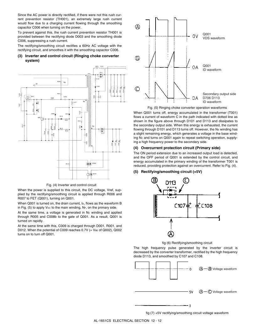
Since the AC power is directly rectified, if there were not this rush cur-rent prevention resistor (TH001), an extremely large rush currentwould flow due to a charging current flowing through the smoothingcapacitor C006 when turning on the power.
To prevent against this, the rush current prevention resistor TH001 isprovided between the rectifying diode D003 and the smoothing diodeC006, suppressing a rush current.
The rectifying/smoothing circuit rectifies a 60Hz AC voltage with therectifying circuit, and smoothes it with the smoothing capacitor C006.
(3) Inverter and control circuit (Ringing choke converter system)
Fig. (4) Inverter and control circuit
When the power is supplied to this circuit, the DC voltage, Vref, sup-plied by the rectifying/smoothing circuit is applied through R006 andR007 to FET (Q001), turning on Q001.
When Q001 is turned on, the drain current, ID, flows as the waveform Bin Fig. (5) to apply VDC to the main winding, NP, on the primary side.
At the same time, a voltage is generated in NC winding and appliedthrough R005 and C008b to the gate of Q001. As a result, Q001 isturned on rapidly.
At the same time with this, C009 is charged through D001, R001, andD012. When the potential of C009 reaches 0.7V (= VBE of Q002), Q002turns on to turn off Q001.
Fig. (5) Ringing choke converter operation waveforms
When Q001 turns off, energy accumulated in the transformer (T001)flows a current of waveform C in the path indicated with dotted line asshown in the figure above through D101 and D113 and dissipates tothe secondary output side. When this energy is exhausted, the currentflowing through D101 and D113 turns off. However, the NS winding hasa slight remaining energy, which generates a voltage in the base wind-ing NC and turns on Q001 again to repeat switching operation, supply-ing a high frequency power to the secondary side.
(4) Overcurrent protection circuit (Primary side)The ON period extension due to an increased output load is detected,and the OFF period of Q001 is extended by the control circuit, andenergy accumulated in the primary winding of the transformer T001 isreduced, providing protection against an overcurrent. Refer to Fig. (4).
(5) Rectifying/smoothing circuit (+5V)
fig (6) Rectifying/smoothing circuit
The high frequency pulse generated by the inverter circuit isdecreased by the converter transformer, rectified by the high frequencydiode D113, and smoothed by C107 and C108.
fig (7) +5V rectifying/smoothing circuit voltage waveform
IDNp
Ns
Nc
Q001VDS waveform
Q001ID waveform
Secondary output sideD706 D113ID waveform
Voltage waveform
Voltage waveform
AL-1651CS ELECTRICAL SECTION 12 - 12

[13] CIRCUIT DIAGRAM1. MCU PWB
R7 *421
R3 *121
X1HC-49U/S19.6608MHz
12
R1811kF
21
R4 *321
R2 *221
R60J
21
C4
12p
12
C220.1u
12
C3 *5
12
C23OPEN
12
C1*6
12
R20
10kF
21
R50J
21
R1OPEN
21
IC1
P2010/PLL701-01
Xin 1
Xout 2
FS0 3
Vss 4SSon5MODOUT6SR07VDD8
IC4
M51957BFP
NC 8
GND4
VCC 7NC1
IN2
NC3
Cd 5OUT 6
R193.3kJ
21
R2210kJ
21
R21 33J21
C2547p
12
BR
2333
J1 2 3 4
8 7 6 5
BR
2233
J1 2 3 4
8 7 6 5
BR
2433
J1 2 3 4
8 7 6 5
BR
2133
J1 2 3 4
8 7 6 5
BR
2033
J1 2 3 4
8 7 6 5
C240.1u
12
R13
10kJ
21
R11
10kJ
21
IC2
HD6412321VF25(H8S/2321)
P3P3P3P3P3P3
PPPP
PP
AVcc103
Vref104
P40/AN0105
P41/AN1106
P42/AN2107
P43/AN3108
P44/AN4109
P45/AN5110
P46/AN6/DA0111
P47/AN7/DA1112
AVss113
Vss114
P17/PO15/TIOCB2/TCLKD115
P16/PO14/TIOCA2116
P15/PO13/TIOCB1/TCLKC117
P14/PO12/TIOCA1118
P13/PO11/TIOCD0/TCLKB119
P12/PO10/TIOCC0/TCLKA120
P11/PO9/TIOCB0/DACK1121
P10/PO8/TIOCA0/DACK0122
MD0123
MD1124
MD2125
PG0/CAS126
PG1/CS3127
PG2/CS2128
PG
3/C
S1
1
PG
4/C
S0
2
Vss
3
NC
4
VC
C5
PC
0/A
06
PC
1/A
17
PC
2/A
28
PC
3/A
39
Vss
10
PC
4/A
411
PC
5/A
512
PC
6/A
613
PC
7/A
714
PB
0/A
815
PB
1/A
916
PB
2/A
1017
PB
3/A
1118
Vss
19
PB
4/A
1220
PB
5/A
1321
PB
6/A
1422
PB
7/A
1523
PA0/
A16
24
PA1/
A17
25
PA2/
A18
26
PA3/
A19
27
Vss
28
PA4/
A20
/IR
Q4
29
PA5/
A21
/IR
Q5
30
PA6/
A22
/IR
Q6
31
PA7/
A23
/IR
Q7
32
P67
/CS
7P/I
RQ
333
P66
/CS
6P/I
RQ
234
Vss
35
Vss
36
P65
/IR
Q1
37
P64
/IR
Q0
38
P53
/AD
TR
G10
2
P52
/SC
K2
101
Vss
100
Vss
99
P51
/RxD
298
P50
/TxD
297
PF
0/B
RE
Q96
PF
1/B
AC
K95
PF
2/LC
AS
/ WA
IT/B
RE
QO
94
PF
3/LW
R93
PF
4/H
WR
92
PF
4/R
D91
PF
6/A
S90
VC
C89
PF
7/0
88
Vss
87
EX
TAL
86
XTA
L85
VC
C84
ST
BY
83
NM
I82
RE
S81
WD
TOV
F80
P20
/PO
0/T
IOC
A3
79
P21
/PO
1/Y
ICO
B3
78
P22
/PO
2/T
IOC
C3
77
P23
/PO
3/T
IOC
D3
76
P24
/PO
4/T
IOC
A4
75
P25
/PO
5/T
IOC
B4
74
P26
/PO
6/T
IOC
A5
73
P27
/PO
7/T
IOC
B5
72
P63
/TE
ND
171
P62
/DR
EQ
170
P61
/TE
ND
0/C
S5
69
Vss
68
Vss
67
P60
/DR
EQ
0/C
S4
66
Vss
65
R12
10kJ
21
C20.1u
12
R9 33J21R8 33J21
R10 100J21
BR110
33J
1234
8765
C38
122
pF1
2C
382
OP
EN 1
2C
383
OP
EN 1
2C
384
OP
EN 1
2
R33733J2 1
C386OPEN1 2
A0 A5
A2
A4
A11
A19
A13A3
A8
A10A7
A12
A16
A14
A18A1
A15
A17A6
A9
CP
UC
LK(N
C)
/TRANSST
SPFMT0
/SCANSP
SPFMT1SPFMT2
/SCANST
SPFMT3
/ST
BY
ES_CMD
RD
/ESS_RDY/ESC_RDY
HWR
/PRINTST
LWR
ESS_TS
RESETOUT1
NM
I
/WD
TOV
F
/CS0#/CS1#/CS2#/CS3#
VCC3
VCC3
VCC3
VCC3
VCC3
VCC3
/PRINTST
/RESET0
/ASIC_RST
/ES_PAGE
MSU_ST1
SPFMT0
SPFMT2/MIRCNT
(SIN2)
SPFMT1
/TRANSST
(KEYIN)
PMCLK
RTH
SPFMT3
/SCANSP
PSL
/SCANST
(SIN3)
(SIN1)
ESS_TS
/ESC_RDY
ES_CMD
/HWR/LWR
/ESS_RDY
/RD
SELIN3SELIN2SELIN1
/RE
SE
T1
/CS3/CS2/CS1/CS0
Spreading Range :+/- 1.25%
R4(*3)
When IC1 is, mounted NOT mounted
OPEN 0J
R3(*1) OPEN 680J
R7(*4) 22J OPEN
R2(*2) 0J OPEN
C3(*5)
C1(*6)
22pF
22pF
15pF
15pF
*R2,R3,C1, and C3 are temtative
(2-D2)(2-E3)
(2-E3)
(2-E3)
(4-C3)(4-C2)
(4-C3)(4-C3)
(2-D1)
(5-B2)
(2-C4)
(8-A2)
(13-B2)
(4-D4)(4-D4)
(4-C3)
(4-D4)
(5-E3)
(4-D4)
(8-A1)
Reset IC
(4-C2)
(8-A3)
(13-B2) (2-C1)
(4-C2)
(3-A2)(4-A2)(2-C1)
(4-C2)
(3-A2)
(8-A3)(8-A2)(8-A2)
(9-B2)
A B
A B
4
3
2
1
MCU PWB (CPU section)
AL-1651CS CIRCUIT DIAGRAM 13 - 1
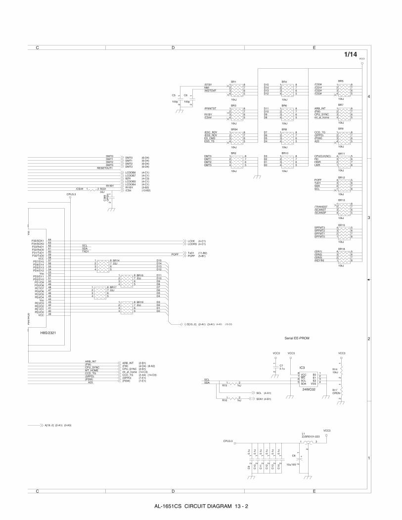
C5
100p
12
C13
0.1u
12
C14
0.1u
12
C10
0.1u
12
C6
100p
12
C8
10u/16V
12
+
C11
0.1u
12
C9
0.1u
12
C12
0.1u
12
BR12
10kJ
1234
8765
L1ZJSR5101-223
1
2
3
BR13
10kJ
1234
8765
BR7
10kJ
1234
8765
BR15
10kJ
1234
8765
BR9
10kJ
1234
8765
BR5
10kJ
1234
8765
BR11
10kJ
1234
8765
BR1433J
1234
8765
BR1933J
1234
8765
BR1633J
1234
8765
BR1733J
1234
8765
C70.1u
12
R1410kJ
21
R17OPEN
21
BR18
10kJ
1234
8765
R16 1kJ21
R15 1kJ21
H8S/2321
P35/SCK1 64
P34/SCK0 63
P33/RxD1 62
P32/RxD0 61
P31/TxD1 60
P30/TxD0 59
VCC 58
PD7/D15 57
PD6/D14 56
PD5/D13 55
PD4/D12 54
Vss 53
PD3/D11 52
PD2/D10 51
PD1/D9 50
PD0/D8 49
PE7/D7 48
PE6/D6 47
PE5/D5 46
PE4/D4 45
Vss 44
PE3/D3 43
PE2/D2 42
PE1/D1 41
PE0/D0 40
VCC 39
P64
/IR
Q0
38V
ss65
IC3
24WC02
E01
E12
E23
VSS4
SDA5 SCL6 WC7 VCC8
BR8
10kJ
1234
8765
BR10
10kJ
1234
8765
BR3
10kJ
1234
8765
BR4
10kJ
1234
8765
BR1
10kJ
1234
8765
BR6
10kJ
1234
8765
BR94
10kJ
1234
8765
BR2
10kJ
1234
8765
C38
5O
PE
N 12
R33133J
21
CPUCLK(NC)
SPFMT1
(FW)
mt_at_home
LWR
/CS0#
/CS2#
CPU_SYNC
/CS1#
SCL
TxD1
SPFMT0
/SCANSP
(SPPD)
/TRANSST
CCD_TG
SDA
(PSW)
SPFMT3
ARB_INT
/SCANST
SPFMT2
HWRRD
A20
(SPPD)
MT_HOMECPU_SYNC
(PSW)
CCD_TG
(FW)ARB_INT
POFF
SCL
/CS3#
TXD1
A20
(SIN3)(SIN2)(SIN1)
(KEYIN)
SDA
SCLSDA
DMT3
/WDTOVFD14
/CS4#
POFF
D8
D5
RY/BY
D1D0
DMT0
D1
D15
D7
D11
D3
D0
D12
D11
RESETOUT1
D13
D8
D3
/CS4#
D10
D4
D7
D5
DMT1
RY/BY D9
DMT2
D6
D2
D9
D14
D6
D4
D10
/STBY
/PRINTST
D12
D15
D2
D13
/ESC_RDY/ESS_RDYES_CMDESS_TS
DMT3
DMT0
DMT2DMT1
NMI
CPU3.3
CPU3.3
VCC3
VCC3
VCC3 VCC3 VCC3
A[19..0]
mt_at_home
RY/BY
(PSW)
CCD_TG
CPU_SYNC
ARB_INT
D[15..0]
(SPPD)
(FW)
SDA1
SCL
POFF
DMT2
LCDDB7LCDDB6
DMT1DMT0
TxD1
LCDRSLCDE
LCDDB5LCDDB4
DMT3
/CS4
BZR
(2-A1) (3-A3)
(2-B1)(4-D4)
(14-C3)
(7-E1)
(2-B1)
(2-A4)
(7-E1)
(2-A1)
(6-D4)(6-D4)(6-D4)(6-D4)
(5-B1)
(3-B2)
(14-D3)
(13-C2)(3-A1) (4-A2)
(4-A1)
(4-B1)
(11-B2)
(4-C3)
(4-C1)(4-C1)
Serial EE-PROM
(4-C1)(4-C1)
(4-C1)(4-C1)
(13-B2)
(8-A2)
C D E
C D E
4
3
2
1
1/14
AL-1651CS CIRCUIT DIAGRAM 13 - 2
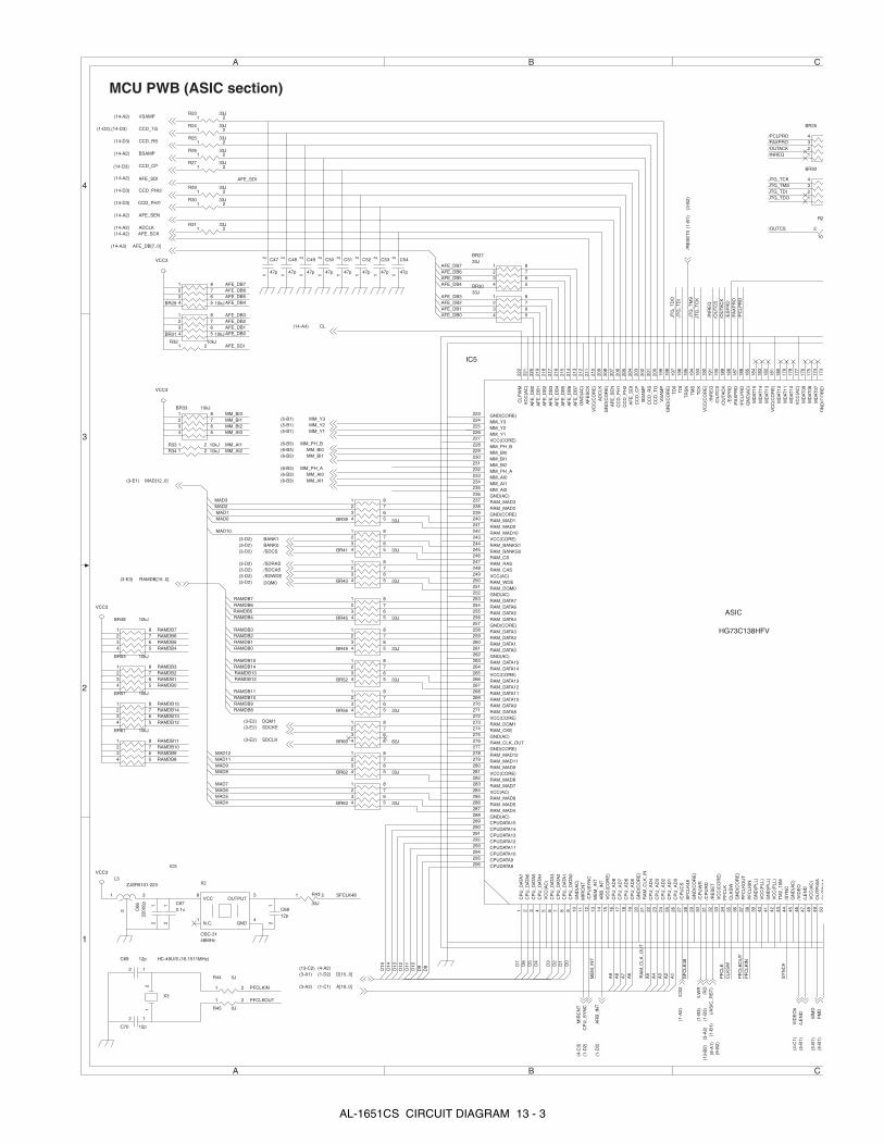
C53
47p
12
R29 33J21
BR2733J
1234
8765
C52
47p
12C51
47p
12 C54
47p
12
R27 33J21
C50
47p
12C49
47p
12
R2
10K
2
BR48 10kJ
1234
8765
BR61 10kJ
1234
8765
BR57 10kJ
1234
8765
BR53 10kJ
1234
8765
C670.1u
12
L3ZJSR5101-223
1
2
3
X2
OSC-3148MHz
N.C.1
VCC8
OUTPUT5
GND4
C6812p
12
C66
2200
0p 12
R43
33J
21
C70 12p
12
C69 12p
12
R45 0J
21X3
HC-49U/S (16.1511MHz)
12
R44 0J
21
R34 10kJ21
BR33 10kJ1234
8765
R33 10kJ21
BR25
1234
BR3033J
1234
8765
R26 33J21
R30 33J21
R31 33J21
R25 33J21
R23 33J21
BR39 33J
1234
8765
BR41 33J
1234
8765
BR43 33J
1234
8765
BR45 33J
1234
8765
BR49 33J
1234
8765
BR52 33J
1234
8765
BR56 33J
1234
8765
BR60 82J
1234
8765
BR62 33J
1234
8765
BR63 33J
1234
8765
R24 33J21
C47
47p
12 C48
47p
12
BR29 10kJ
1234
8765
BR31 10kJ
1234
8765
R32 10kJ21
BR93
1234
IC5
HG73C138HFV
ASIC
CP
U_D
ATA
71
CP
U_D
ATA
62
CP
U_D
ATA
53
CP
U_D
ATA
44
CP
U_D
ATA
18
CP
U_D
ATA
36
CP
U_D
ATA
27
VC
C(A
C)
5
CP
U_D
ATA
09
GN
D(A
C)
10
MIR
CN
T11
/CP
US
YN
C12
ME
M_I
NT
13
AR
B_I
NT
14
VC
C(C
OR
E)
15
CP
U_A
D8
16
CP
U_A
D7
17
CP
U_A
D6
18
CP
U_A
D5
19
GN
D(C
OR
E)
20
RA
M_C
LK_I
N21
CP
U_A
D4
22
CP
U_A
D3
23
CP
U_A
D2
24
CP
U_A
D1
25
CP
U_A
D0
26
/CP
UC
S27
SF
CLK
4828
GN
D(C
OR
E)
29
/CP
UW
R30
/CP
UR
D31
/RE
SE
T32
PF
CLK
34
CLK
SW
35
GN
D(C
OR
E)
36
PF
CLK
OU
T37
PF
CLK
IN38
GN
D(P
LL)
39
VC
C(P
LL)
40
GN
D(P
LL)
41
VC
C(P
LL)
42
TM
2_15
M43
/SY
NC
44
GN
D(A
C)
45
/VID
EO
46
/LE
ND
47
VC
C(A
C)
48
OU
TP
00A
49
VC
C(C
OR
E)
192
/INR
EQ
191
/OU
TC
S19
0
/OU
TAC
K18
9
/ES
PR
D18
8
/FA
XP
RD
187
/PC
LPR
D18
6
GN
D(A
C)
185
MD
AT15
184
MD
AT14
183
MD
AT13
182
VC
C(C
OR
E)
181
MD
AT12
180
MD
AT11
179
MD
AT10
178
VC
C(A
C)
177
MD
AT09
176
MD
AT08
175
MD
AT07
174
GN
D(C
OR
E)
173
RAM_DATA4256RAM_DATA5255RAM_DATA6254RAM_DATA7253GND(AC)252RAM_DQM0251RAM_WDE250VCC(AC)249RAM_CAS248RAM_RAS247RAM_CS246RAM_BANKS0245RAM_BANKS1244VCC(CORE)243RAM_MAD10242RAM_MAD0241RAM_MAD1240GND(CORE)239RAM_MAD2238RAM_MAD3237GND(AC)236MM_AI2235MM_AI1234MM_AI0233MM_PH_A232
AF
E_D
B3
217
MM_BI2231MM_BI1230
MM_Y2225
VC
C(A
C)
221
MM_Y1226
AF
E_D
B0
220
AF
E_D
B1
219
GND(CORE)223
AF
E_D
B2
218
AF
E_D
B4
216
AF
E_D
B5
215
MM_BI0229MM_PH_B228VCC(CORE)227
MM_Y3224
CLP
WM
222
AF
E_D
B6
214
AF
E_D
B7
213
GN
D(A
C)
212
AF
ES
CK
211
VC
C(C
OR
E)
210
AD
CLK
209
GN
D(C
OR
E)
208
AF
E_S
EN
207
CC
D_P
H1
206
CC
D_P
H2
205
AF
E_S
DI
204
CC
D_C
P20
3
BS
AM
P20
2
CC
D_R
S20
1
CC
D_T
G20
0
VS
AM
P19
9
GN
D(C
OR
E)
198
TD
019
7
TR
SK
195
TD
I19
6
TC
K19
3T
MS
194
VC
C(C
OR
E)
33
OU
TP
01A
50
GND(CORE)257
RAM_DATA3258
RAM_DATA2259
RAM_DATA1260
RAM_DATA0261
GND(AC)262
RAM_DATA15263
RAM_DATA14264
VCC(CORE)265
RAM_DATA13266
RAM_DATA12267
RAM_DATA11268
RAM_DATA10269
RAM_DATA9270
RAM_DATA8271
VCC(CORE)272
RAM_DQM1273
RAM_CKE274
GND(AC)275
RAM_CLK_OUT276
GND(CORE)277
RAM_MAD12278
RAM_MAD11279
RAM_MAD9280
VCC(CORE)281
RAM_MAD8282
RAM_MAD7283
VCC(AC)284
RAM_MAD6285
RAM_MAD5286
RAM_MAD4287
GND(AC)288
CPUDATA15289
CPUDATA14290
CPUDATA13291
CPUDATA12292
CPUDATA11293
CPUDATA10294
CPUDATA9295
CPUDATA8296
RAMDB0RAMDB1RAMDB2RAMDB3
RAMDB4RAMDB5RAMDB6RAMDB7
RAMDB15RAMDB14RAMDB13RAMDB12
RAMDB11RAMDB10RAMDB9RAMDB8
SFCLK48
PFCLKIN
PFCLKOUT
MM_BI2MM_AI0
MM_BI1
MM_AI2
MM_BI0
MM_AI1
/INREQ/OUTACK/FAXPRO/PCLPRO
/OUTCS
A8
D9
/OU
TC
S
/PC
LPR
O
RAMDB13
D7
RA
M_C
LK_O
UT
AFE_SDI
D4
D2
ME
M_I
NT
RAMDB14
D8
PF
CLK
IN
/FA
XP
RO
D15
PF
CLK
OU
T
D3
D0
A7
A6
A5
CLK
SW
RAMDB9/IN
RE
Q
D1
D13 D
5
JTG
_TD
I
D12
D11
RAMDB12
A4
A2
A1
/OU
TAC
K
A9
A3
RAMDB1
D6
SF
CLK
48
RAMDB15
D10
PF
CLK
SY
NC
#
D14
JTG
_TD
O
RAMDB2
/ES
PR
D
MAD8
MAD0
MAD10
MAD3MAD2MAD1
MAD6
MAD9
RAMDB7RAMDB6RAMDB5RAMDB4
RAMDB3
RAMDB0
RAMDB11RAMDB10
RAMDB8
MAD12MAD11
MAD7
MAD5MAD4
AFE_DB2
AFE_DB7
AFE_DB0
AFE_DB6
AFE_DB3
AFE_DB4
AFE_DB1
AFE_DB5AFE_DB7AFE_DB6AFE_DB5AFE_DB4
AFE_DB3AFE_DB2AFE_DB1AFE_DB0
AFE_SDI
JTG
_TM
SJT
G_T
CK
JTG_TDIJTG_TMSJTG_TCK
JTG_TDO
VCC3
VCC3
VCC3
VCC3
AFE_SEN
ADCLK
CCD_CP
CCD_PHI1
CCD_PHI2
CCD_TG
AFE_DB[7..0]
CL
CCD_RS
VSAMP
AFE_SCK
AFE_SDI
BSAMP
MM_Y1
MM_PH_AMM_AI0MM_AI1
MM_PH_BMM_BI0MM_BI1
MM_Y2MM_Y3
BANK1BANK0
/SDCAS/SDRAS
/SDCS
DQM0
MAD[12..0]
/SDWDE
SDCKEDQM1
SDCLK
D[15..0]
A[19..0]
/CS
2
MIR
CN
TC
PU
_SY
NC
/LW
R/R
D
RAMDB[15..0]
PM
D
AR
B_I
NT
MM
D
C(/A
SIC
_RS
T)
/LE
ND
VID
EO
#
/RE
SE
T0
(14-D3)
(1-D2),(14-D3)
(14-A3)
(14-A4)
(14-D3)
(14-A2)
(14-A2)
(14-D3)
(14-D3)
(14-A2)
(14-A2)
(14-A2)
(14-A2)
(5-B1)(5-B1)
(6-B3)(6-B3)(6-B3)
(6-B3)(6-B3)(6-B3)
(5-B1)
(3-E2)
(3-E3)
(3-D2)(3-D2)
(3-D2)
(3-D2)
(3-D2)
(3-D2)(3-D2)
(3-E1)
(3-E2)(3-E2)
(1-D2)
(1-C1)
IC5
(5-B
1)
(1-A
2)
(4-C
3)
(1-D
2)
(1-D
2)
(1-B
3)(1
-B3)
(1-B
1)
(5-B
1)(5
-B1)
()
(3-A1)(4-A2)(13-C2)
(3-A3)
(3-A
2)(1
3-B
2)
(8-A
1)
(4-C
1)
(1-B
1)
(9-B
2)
(3-B
2)
A B C
A B C
4
3
2
1
MCU PWB (ASIC section)
AL-1651CS CIRCUIT DIAGRAM 13 - 3
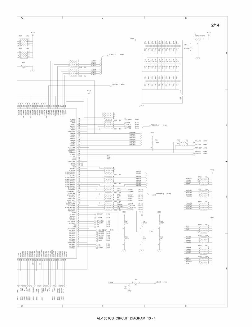
R28
10KJ
2 1BR26 33J
1234
8765
BR28 33J
1234
8765
BR34 33J
1234
8765
BR32 33J
1234
8765
BR47 33J
1234
8765
BR51 33J
1234
8765
BR44 33J
1234
8765
BR58 33J
1234
8765
BR55 33J
1234
8765
R4110kJ
21
R40OPEN
21
R3710kJ
21
R38OPEN
21
R4210kJ
21
R39OPEN
21
R46
10J
21
BR59 10kJ1234
8765
BR46 10kJ1234
8765
BR50 10kJ1234
8765
BR54 10kJ1234
8765
BR40 10kJ1234
8765
BR37 10kJ1234
8765
BR35 10kJ1234
8765
C36
47u/16V
12
+
L2ZJSR5101-102TA
1
2
3
C26
0.1u
12
C30
0.1u
12
C28
0.1u
12
C29
0.1u
12
C31
0.1u
12
C32
0.1u
12
C33
0.1u
12
C34
0.1u
12
C35
0.1u
12
C38
0.1u
12
C41
0.1u
12
C39
0.1u
12
C40
0.1u
12
C37
0.1u
12
C42
0.1u
12
C43
0.1u
12
C44
0.1u
12
C45
0.1u
12
C46
0.1u
12
C55
0.1u
12
C62
0.1u
12
C59
0.1u
12
C64
0.1u
12
C63
0.1u
12
C60
0.1u
12
C56
0.1u
12
C58
0.1u
12
C57
0.1u
12
C61
0.1u
12
C27
0.1u
12
BR25 10KJ
1234
8765
C7147p
12
C65
0.1u
12
R310 10J2 1
R311 10J2 1
BR93 10KJ
1234
8765
R35
10kJ
21
/LE
ND
47
VC
C(A
C)
48
OU
TP
00A
49
OU
TP
02A
51
OU
TP
03A
52
OU
TP
04A
53
OU
TP
05A
54
OU
TP
06A
55
VC
C(C
OR
E)
57O
UT
P15
A56
OU
TP
07A
58
OU
TP
08A
59
GN
D(C
OR
E)
60
OU
TP
09A
61
OU
TP
10A
62
OU
TP
11A
63
OU
TP
12A
64
VCC(CORE)86
OUTP13B84
OUTP12B83
OUTP10B81
GN
D(A
C)
69
OUTP09B80
OUTP08B79
OU
TP
03B
72
GND(CORE)78
OUTP07B77
OUTP06B76
OU
TP
00B
68O
UT
P14
A67
VC
C(C
OR
E)
66O
UT
P13
A65
VC
C(A
C)
74O
UT
P04
B73
OUTP11B82
OU
TP
02B
71
OUTP05B75
OUTP14B85
OU
TP
01B
70
TSP_MODE96
OPE_CLK92
/TM87
TM88
OPE_DATA89
OPE_LATCH90
GND(AC)91
VCC(AC)93
/SCANSP94
TSO095
IE1284_STB97
IE1284_AUTOFD98
VCC(CORE)99
IE1284_SLCTIN100
IE1284_INIT101
IE1284_SLCT102
GND(CORE)103
IE1284_PE104
IE1284_BUSY105
IE1284_ACK106
IE1284_FAULT107
VCC(CORE)108
IE1284_REV109
IE1284_PARAD7110
IE1284_PARAD6111
IE1284_PARAD5112
IE1284_PARAD4113
IE1284_PARAD3114
IE1284_PARAD2115
VCC(AC)116
IE1284_PARAD1117
IE1284_PARAD0118
SUSPEND119
GND(AC)120
OEN121
VMOUT122
VPOUT123
GND(CORE)124
VMIN125VPIN126
RCV127
/SCANST128
MD
AT09
176
MD
AT08
175
MD
AT07
174
GN
D(C
OR
E)
173
MD
AT06
172
MD
AT05
171
MD
AT04
170
VC
C(C
OR
E)
169
MD
AT03
168
MD
AT02
167
MD
AT01
166
MD
AT00
165
GN
D(A
C)
164
/INC
S16
3
/INA
CK
162
/OU
TR
EQ
161
GN
D(C
OR
E)
160
/HS
YN
C15
9
PID
ATA
015
8
PID
ATA
115
7
PID
ATA
215
6
VC
C(A
C)
155
PID
ATA
315
4
PID
ATA
415
3
PID
ATA
515
2
PID
ATA
615
1
PID
ATA
715
0
/PO
CS
149
/POREQ148
VCC(AC)147
/PIWT146
/PIACK145
GND(AC)144
/POACK143
/PIREQ142
GND(CORE)141
PODATA0140
PODATA1139
PODATA2138
PODATA3137
PODATA4136
PODATA5135
PODATA6134
PODATA7133
VCC(CORE)132
/TRANSST131
/RECEPTST130
/PRINTST129
OU
TP
01A
50
PIDATA4
PIDATA0
PIDATA5PIDATA6
PIDATA1
PIDATA7
PIDATA2PIDATA3
/REV
/INIT/SLCTIN/AUTOFD/STB
/ACKBUSYPE
/FAULT
SLCT
PARAD1
PARAD2
PARAD6PARAD7
PARAD4PARAD3
PARAD5
PARAD0
/INIT/SLCTIN/AUTOFD/STB
PARAD7PARAD6PARAD5PARAD4
PARAD3PARAD2PARAD1PARAD0
VPINRCV
VMIN
/POREQ/PIREQ
PODATA0PODATA1PODATA2PODATA3
PODATA4PODATA5PODATA6PODATA7
CLKSWMEM_INT
PODATA5
PODATA7
PFCLK
SYNC#
PODATA3
PODATA1PODATA2
PODATA4
PODATA6
PODATA0
RCVVPINVMIN
G3.3V
VCC3VCC3 VCC3
VCC3
VCC3
VCC3
G3.3V
VCC3
VCC3
/H_SYNC
PIDATA[7..0]
PODATA[7..0]/POACK/PIREQ
/POREQ
/PIACK/PIWR
/SCANSP
/SCANST
/TRANSST
/PRINTST
/REV
/INIT
/ACKBUSYPE
/FAULT
SLCT
/SLCTIN
/STB
PARAD[7..0]
/AUTOFD
OP_CLK
TMTM_
OP_LATCHOP_DATA
(/SYNC)
CPFS2PRHL
MPFSMIRONSPFONKEYSC1
KEYSC3KEYSC2
SP
US
SP
FS
VF
M
MR
PS
1
MC
PM
D
CP
FS
1
DE
VD
IR
MR
PS
3
VF
MC
NT
LDE
N
GR
IDL
MM
D
RR
S
SR
RC
MR
PS
2
BIA
S
TC
/LE
ND
/PR_LINE
/SC_LINE
/IMC_READY
/FP
OF
F
SG
S
(1-B3)(1-A2)
(1-A2)
(12-A3)
(4-C3)
(4-C3)
(4-C3)
(4-C2)(4-C2)
(4-D4)
(5-B
1)
(5-B
1)(5
-B1)
(5-B
4)(5
-B4)
(5-B
4)
(5-B
3)
(5-B
3)(5
-B2)
(5-B
2)(5
-B2)
(5-B
2)(5
-B3)
(5-B3)(5-B3)(5-B2)
(5-B3)(4-C2)(4-C2)
(4-A
1)
(4-C2)(4-C2)(4-C2)
(8-A2)
(4-C3)
(12-A3)
(8-A2)
(8-A2)
(8-A2)
(8-A4)(8-A2)(8-A4)(8-A4)
(8-A2)
(8-A2)
(8-A4)
(12-A3)
(12-A3)(12-A3)(12-A3)(12-A3)
(12-A3)(12-A3)(12-A3)(12-A3)
(5-B
4)
(5-B
3)
C D E
C D E
4
3
2
1
2/14
AL-1651CS CIRCUIT DIAGRAM 13 - 4

R4910kJ
R51 0J21
R48
0J2
1
R47
10kJ
21
IC7
Flash ROM
A025A124
A223A322A421A520A619A718
A88A97A106A115A124A133A142A151
A1648
A1717
DQ029
DQ131
DQ233
DQ335
DQ438
DQ540
DQ642
DQ744
DQ830
DQ932
DQ1034
DQ1136
DQ1239
DQ1341
DQ1443
DQ1545
NC9
NC10
NC16
GND46
GND27
VCC37
VPP13
BYTE47
OE28
CE26
WE11
RP12
WP14
RY/BY15
R52
OP
EN
21
R53
OP
EN
21
C74
0.1u
12
C73
0.1u
12
IC8
IS63LV1024L-12J-TR
I/O06
A01
I/O17
A12
I/O210
A23
I/O311
A34
I/O422
A413
I/O523
A514
I/O626
A615
I/O727
A716
A817
A918
A1019
A1120
A1221
A1329
A1430
CS15
OE28
WE12
VDD8
GND9
VDD24
A1531
A1632
GND25
HWRZ
A12
A7
A10A11
A17
A9
A12
A5
A16
A14A1
D14D15
RDZ
A15
A8
A6
D10A2
A4
A10
A14A13
A15
A3
D8
D12
A6
A16
A7
A11
CS1Z
A2
A4
A8
HWRZ
D9
D11A13
A9
A18A19
D13A5
A1
A0
A3
VCC3
VCC3VCC3
D[15..0]
/CS1/RD
/HWR
A[19..0]
RY/BY
/RESET0
(2-A1)
(1-D2)
(1-A2)(1-B3)(1-B3)
(1-D3)
Flash ROM
LH28F400BVE-BL85
R51 OPEN
IC7
(1-C1)
(2-C1)(15-B2)
(2-A1)(4-A2)(15-C2)
A B
A B
4
3
2
1
MCU PWB (Memory section)
AL-1651CS CIRCUIT DIAGRAM 13 - 5
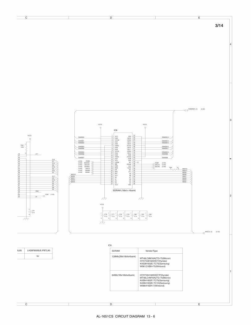
R50 0J21
C750.1u
12
R4910kJ
21
C760.1u
12
C770.1u
12
C780.1u
12
C790.1u
12
C800.1u
12
C810.1u
12
C820.1u
12
IC6
SDRAM (16bit x 4bank)
A023
A124
A225
A326
A429
A530
A631
A732
A833
A934
A1022
BA020
DQ02
DQ14
DQ25
DQ37
DQ48
DQ510
DQ611
DQ713
DQ842
DQ944
DQ1045
DQ1147
DQ1248
DQ1350
DQ1451
DQ1553
VCC1
VCC27
VSS54
VSS28
VCCQ9
VSS41
VCCQ43
VCCQ49
VSSQ6
VSSQ12
VSSQ46
VSSQ52
LDQM15
UDQM39
WE16
CAS17
RAS18
CS19
CLKE37
CLK38
NC40
NC36
VCCQ3
VCC14
BA121
A1135
25
48
29
31
33
35
38
40
42
44
30
32
34
36
39
41
43
4546
27
37
47
28
26
RAMDB0
RAMDB9RAMDB10
RAMDB11RAMDB12
RAMDB13RAMDB14
RAMDB15
RAMDB7 RAMDB8
RAMDB3
RAMDB1
RAMDB5RAMDB6
RAMDB2
RAMDB4
MAD8MAD9
MAD4MAD5
MAD11
MAD1MAD0MAD10
MAD7
MAD12
A17
A1
RDZ
MAD3MAD2
MAD6
D4
D8
D14
D5
D9
D10D2
D15
D3
D6
D12
D1
D11
D0
D13
D7
VCC3
VCC3
VCC3VCC3
/CS0
MAD[12..0]
BANK0BANK1
/SDCS
/SDWDE/SDCAS/SDRAS
DQM0DQM1SDCLKSDCKE
RAMDB[15..0]
(1-A2)
(2-A2)
(2-A3)
SDRAM Vendor/Type
128Mb(2Mx16bitx4bank)
BL85 LH28F800BJE-PBTL90
0J
IC6
(2-A2)(2-A2)(2-A2)(2-A3)(2-A3)(2-A3)
(2-A2)(2-A2)(2-A2)
(2-A2)
64Mb(1Mx16bitx4bank)
MT48LC8M16A2TG-75(Micron) HY57V281620HCT(Hyndai) K4S281632E-TC75(Samsung) W981216BH-75(Winbond)
HY57V641620HGT-P(Hyndai) MT48LC4M16A2TG-75(Micron) K4S641632F-TC75(Samsung) K4S641632E-TC1H(Samsung) W986416DH-7(Winbond)
C D E
C D E
4
3
2
1
3/14
AL-1651CS CIRCUIT DIAGRAM 13 - 6

C83
0.1u
12
R56
10J21
C84
33p
12
C87
0.1u
12
R57
10J
21
C88
33p
12
C90
0.1u
12
R60
10J
21
C91
33p
12
R5910kJ
21
IC9
74HC151
D04
D13
D22
D31
D415
D514
D613
D712
A11
B10
C9
G7
W 6
Y 5
VCC 16
GND 8
IC11
74HC151
D04
D13
D22
D31
D415
D514
D613
D712
A11
B10
C9
G7
W 6
Y 5
VCC 16
GND 8
IC13
74HC151
D04
D13
D22
D31
D415
D514
D613
D712
A11
B10
C9
G7
W 6
Y 5
VCC 16
GND 8
IC15
74LCX574
D12
D23
D34
D45
D56
D67
D78
D89
CLK11
OC1
Q1 19
Q2 18
Q3 17
Q416
Q5 15
Q6 14
Q713
Q812
VCC20
GND10
IC17
NC7S32M5X
1
24
53
C94
0.1u
12
C93
0.1u
12
BR68
10kJ
1234
8765
R5510kJ
21
C109
0.1u
12
C1030.1u
12
IC20
NC7ST08M5X
1
24
R30810kJ
21
R30910kJ
21
R31
510
kJ 21R
317
10kJ 2
1
IC18
TC7SBD385AFU
A1 B 2
OE4
GND3
Vcc 5
R33610kJ
21
C38
947
pF1
2
R34433J
21R34533J
21R34633J
21
C39
033
pF1
2C
391
33F
R3470J
21R3480J
21R3490J
21R3500J
21
C39
3O
PE
N1
2C
394
OP
EN
12
C39
5O
PE
N1
2C
396
OP
EN
D15
D11
D8
D10
D12
D9
D13D14
/RESET#
5V
5V
5V5V
VCC3
VCC3
VCC3
EN5V
VCC3
EN5V
VCC3
EN5V
SIN1SIN2SIN3
SELIN1SELIN2SELIN3
OP_CLKOP_DATA
SPFMT0SPFMT1
SPFMT3MIRONSPFON
TMTM_
SIN1
SIN2
(SELIN1)(SELIN2)(SELIN3)
(PPD1)(POD)(MFD)
(CED1)(TCS)
(PMRDY)DVS1
(DRST)
(PPD2)(PPD3)
THOPEN(CED2)DSWS
(MMLD)
(SDSW)(SPID)(SB4D)
FW
SPFMT2/MIRCNT
SIN3
MIRCNT
LCDDB7LCDDB6LCDDB5LCDDB4
LCDELCDRS
D[15..0]
/HWR
/CS3
SFTMT0SFTMT1SFTMT2SFTMT3
KEYSC1KEYSC2KEYSC3
KEYIN
DEVDIR
(SCL1)
SDA1(SDA1)
OP_LATCHPSL
(SDOD)(PD1)(PD2)
SCL
BZR
MCNT
/RESET0
/ASIC_RST
SPFSSRRCSGSSPUS
(7-E1)
(7-E2)
(7-E3)
(4-E2)
(7-E1)
(7-E2)
(7-E3)
(7-E4)
(7-E4)
(7-E4)
(7-E3)(7-E4)(7-E3)(7-E1)
(7-C4)
(5-E2)
(7-E4)
(11-D3)(7-E4)
(4-C4)
(4-C4)
(4-C4)
(10-C4)
(2-D2)(2-D2)
(2-D2)
(1-B3)(1-B3)(1-B3)
(1-A2)(1-A2)(1-A2)(1-A2)
(4-C3)
(2-D1)(2-D1)
Digital Input Multiplexer
3
3
3.3V
5V/3.3V
(1-D2)
(3-A2)
Extension Digital Output Port
5V
5V
3.3V
3.3V
For CRUM Model Only
(4-E2)(4-E2)
(10-E3)(10-E3)(10-E3)
(7-E4)
(3-A1) (2-A1)(15-C2)
(1-A2)
(1-B3)
(6-D3)(6-D3)(6-D3)(6-D3)
(2-C1)
(1-E2) (11-D3)
(2-D2)(2-D2)(1-A2)
(2-D1)(2-D1)(2-D1)
(1-D3)(1-D3)(1-D3)(1-D3)(1-D3)(1-D3)
(1-D3)
(7-E4)
A B C
A B C
4
3
2
1
MCU PWB (Driver section 1)
AL-1651CS CIRCUIT DIAGRAM 13 - 7
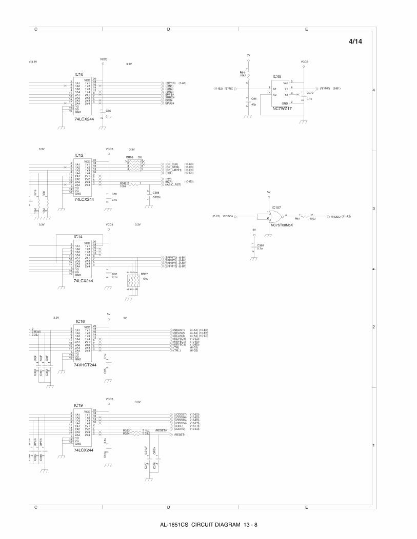
C86
0.1u
12
C920.1u
12
C89
0.1u
12
BR67
10kJ
1234
8765
IC10
74LCX244
1A12
1A24
1A36
1A48
2A111
2A213
2A315
2A417
1G1
2G19
1Y1 18
1Y2 16
1Y3 14
1Y412
2Y1 9
2Y2 7
2Y3 5
2Y43
VCC20
GND10
C10
40.
1u1
2C
950.
1u1
2
IC16
74VHCT244
1A12
1A24
1A36
1A48
2A111
2A213
2A315
2A417
1G1
2G19
1Y118
1Y2 16
1Y3 14
1Y412
2Y19
2Y2 7
2Y3 5
2Y43
VCC 20
GND10
R61 100J21
R58
10kJ 2
1
BR88 33J1234
8765
IC14
74LCX244
1A12
1A24
1A36
1A48
2A111
2A213
2A315
2A417
1G1
2G19
1Y1 18
1Y2 16
1Y3 14
1Y412
2Y1 9
2Y2 7
2Y35
2Y43
VCC20
GND10
R31
510
kJ 21
IC12
74LCX244
1A12
1A24
1A36
1A48
2A111
2A213
2A315
2A417
1G1
2G19
1Y1 18
1Y216
1Y3 14
1Y4 12
2Y1 9
2Y27
2Y3 5
2Y4 3
VCC 20
GND10
IC19
74LCX244
1A12
1A24
1A36
1A48
2A111
2A213
2A315
2A417
1G1
2G19
1Y118
1Y216
1Y3 14
1Y4 12
2Y19
2Y2 7
2Y3 5
2Y4 3
VCC 20
GND10
IC45
NC7WZ17
A11
A23
Y1 6
Y2 4
GND2
Vcc 5
C85
47p
12
R5410kJ
21
C379
0.1u
12
R323 1kJ21
C37
70.
01uF
12
R324 33J21
C37
8O
PE
N1
2
IC107
NC7ST08M5X
1
24
C3800.1u
12
12
2R34533J
22
C39
033
pF1
2C
391
33pF
12
C39
233
pF1
2
C39
4O
PE
N1
2C
395
OP
EN
12
C39
6O
PE
N1
2
R342100J
12
C388
OPEN
12
/RESET#
VCC3
VCC3
5V
VCC3
VCC3
5V
VCC3
5V
5V
(KEYIN)
(FW)
(SIN1)(SIN2)(SIN3)
(SELIN1)(SELIN2)(SELIN3)
(OP_DATA)(OP_LATCH)
(SPFMT0)(SPFMT1)(SPFMT2)(SPFMT3)
(TM)(TM_)
(LCDDB7)(LCDDB6)(LCDDB5)(LCDDB4)(LCDE)(LCDRS)
(KEYSC1)(KEYSC2)(KEYSC3)
/VIDEOVIDEO#
(OP_CLK)
(PSL)
(BZR)
/SYNC (/SYNC)
/RESET1
(/ASIC_RST)
SPFS#SRRC#SGS#SPUS#
(1-A3)
(4-A4)
(10-E3)
(10-E3)
(6-D2)(6-D2)
(6-B1)(6-B1)(6-B1)(6-B1)
3.3V
3.3V
3.3V 3.3V
V/3.3V
5V3.3V
3.3V
(10-E3)(10-E3)(10-E4)
(4-A4) (10-E3)(4-A4) (10-E3)(10-E3)(10-E3)(10-E3)
(2-C1)
(10-E3)(10-E3)(10-E3)(10-E3)(10-E3)(10-E3)
(10-E3)
(11-A2)
3.3V
(11-B2) (2-E1)
C D E
C D E
4
3
2
1
4/14
AL-1651CS CIRCUIT DIAGRAM 13 - 8
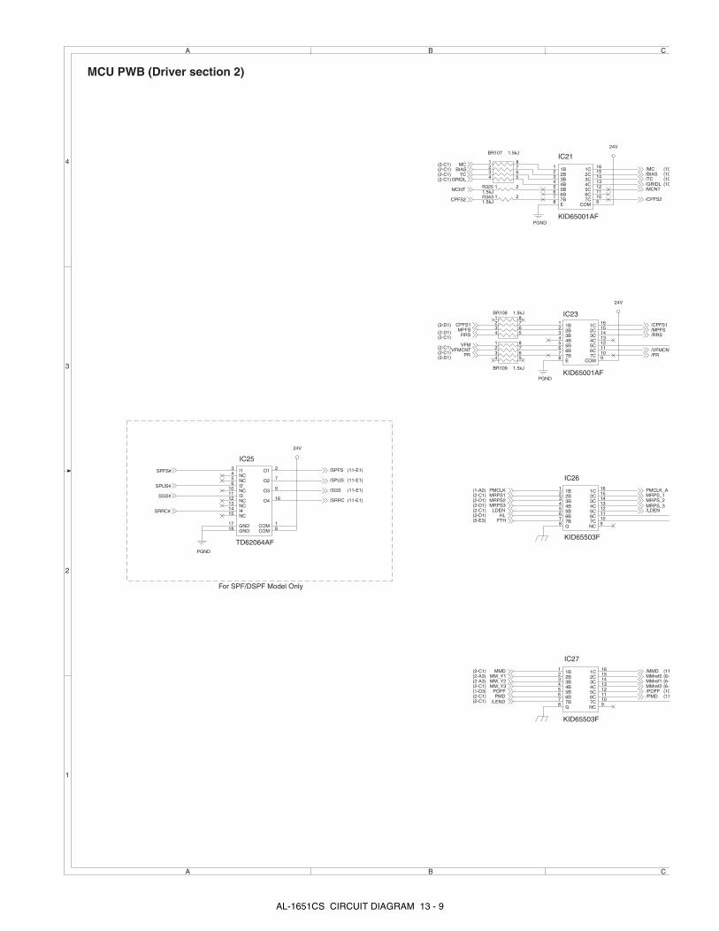
IC23
KID65001AF
1B1
2B2
3B3
4B4
5B5
6B6
7B7
E8 COM 9
1C 16
2C15
3C14
4C 13
5C 12
6C11
7C 10
IC25
TD62064AF
I13
NC4
NC5
I26
NC10
I311
NC12
NC13
GND17
O1 2
O2 7
O3 9
O4 16
COM 1
COM 8GND18
I414
NC15
IC26
KID65503F
1B1
2B2
3B3
4B4
5B5
6B6
7B7
G8 NC 9
1C 16
2C 15
3C14
4C 13
5C 12
6C11
7C10
IC27
KID65503F
1B1
2B2
3B3
4B4
5B5
6B6
7B7
G8
NC9
1C 16
2C 15
3C 14
4C13
5C 12
6C 11
7C 10
IC21
KID65001AF
1B1
2B2
3B3
4B4
5B5
6B6
7B7
E8
COM9
1C 16
2C 15
3C 14
4C13
5C 12
6C 11
7C10
BR107 1.5kJ
1234
8765
BR109 1.5kJ
1234
8765
BR108 1.5kJ1234
8765
R3251.5kJ
21
R3431.5kJ
21
PGND
PGND
PGND
24V
24V
24V
MCBIAS
TCGRIDL
CPFS1MPFS
RRS
VFMVFMCNT
MRPS1
HLLDEN
PMCLK
PMD
PR
FTH
MM_Y2
MMDMM_Y1
MM_Y3
SPUS#
SPFS#
SRRC#
SGS#
/MC/BIAS/TC/GRIDL
/CPFS1/MPFS/RRS
/PR/VFMCNT
PMCLK_A
/PMD
MRPS_1
/LDEN
MMref1
/MMD
MMref2
MMref0
/SGS
/SPUS
/SRRC
/SPFS
MRPS_2
POFF /POFF
MRPS2MRPS3 MRPS_3
/LEND
MCNT /MCNT
CPFS2 /CPFS2
For SPF/DSPF Model Only
(11-E1)
(2-C1)(2-C1)(2-C1)(2-C1)
(10
(10(10
(10
(2-C1)(2-D1)
(2-D1)
(2-C1)
(2-D1)(2-C1)
(5-E3)(2-D1)(2-C1)(2-D1)(2-D1)(2-C1)(1-A2)
(10(11
(11
(6-A(6-A(6-A
(2-C1)
(2-C1)
(2-C1)
(2-A3)
(2-C1)
(2-A3)
(1-D3)
(11-E1)
(11-E1)
(11-E1)
A B C
A B C
4
3
2
1
MCU PWB (Driver section 2)
AL-1651CS CIRCUIT DIAGRAM 13 - 9

R687.5kF
21
R714.3kF
21
D1
MA700
1 2
R671MF
21
R661kF
21
R7010kF
21
R691kJ
21
C11122000p
12 C113
0.1u
12
R81300J 21
R82100J 21
C112
0.1u
12
R831.2kF
21
R8510kF
21
R8410kJ
21
C114
22000p
12
D4
1SS355
12
R73
47kJ21
R78
4.7kJ1/4W
21
R86240J
21
R87240J
21
IC22AKIA393F
3
21
84
+
-
C110
0.1u
12
IC22BKIA393F
5
67
84
+
-
IC24AKIA358F
3
21
84
+
-
IC24BKIA358F
5
67
84
+
-
Q2KRA119S 1
2
3
Q1KTA1505S
Q3KRC106S
1
2
3
R8810kJ
21
D2
KDS226
2
13
D3
KDS226
2
13
D40
1SS355
12
12V
24V
INT5V
12VVCC3
VCC3 VCC3
12VVCC3
12V
12V
12V
VCC3
5V
5V
PGND
CAS
CRIDL
VFMOUT
HLOUT
/CPFS1/MPFS/RRS
/PR/VFMCNT
MCLK_A
MD
RPS_1
DEN
Mref1
MD
Mref2
Mref0
RPS_2
FTH
RTH
THOPEN
RTH_IN
OFF
RPS_3
SHOLD
CNT
PFS2
(10-A4)
(10-A4)(10-B4)
(10-B4)
(10-A3)(11-A3)
(11-A3)
(11-B3)
(11-B2)
(11-B2)
(6-A1)(6-A1)(6-A1)
(10-B3)
(10-B4)(11-B2)
(11-B2)
(11-A4)
(6-A3)(6-A3)(6-A3)
(1-A3)
(4-A4)
(5-B2)
(11-C1)
C D E
C D E
4
3
2
1
5/14
AL-1651CS CIRCUIT DIAGRAM 13 - 10

R107300J
21
C125 2200p
1 2
R99 7.5kJ21
C126 2200p1 2
R100 7.5kJ
21
C132
2200p
12
C136
OPEN
12
C130
OPEN
12
C127 OPEN
1 2
C137 OPEN1 2
C135
2200p
12
R104 2.4kJ
21
R111 2.4kJ21
R1011kJ
21
R1151kJ
21
C134
0.1u
12
R108620J
21
R1091.2kJ
21
R110100J
21
R102750J
21
C116820p
1 2
C117820p
12
C118820p
12
C1210.1u
12
C115820p
1 2
C1190.1u
12
R921.5kJ
21
R90
0.68J1W
21
R9430kJ
21
R9530kJ
21
R911.5kJ
21
R89
0.68J1W
21
R98510J
21
R971kJ
21
R962kJ
21
R103 1J 2W
21
R931kJ
21
IC31
MTD1361/F
CrA23
CrB20
VsA25
RsA3
VrefA24
VrefB19
RsB12
VsB18
In /A26
In A27
In /B17
In B16
Vmm 22
OUT /A1
OUT A 4
OUT /B 14
OUT B11
PG 15
PG 28
IC29
L6219DS or AMM56219
OUT 2A2
SENSE 23
COMP 24
OUT 2B5
GND6
GND7
I028
I129
PHASE 210
VREF 211
RC 212 VSS 13RC 1 14VREF 1 15PHASE 116I11 17GND 18GND 19I0120OUT 1B 21COMP 1 22SENSE 123VS24
OUT 1A1
R114 1J 2W21
C1230.1u/50V
12
C120.1u/50
CP20603FA1.5A
1 2
PGND
PGND
PGND
PGND
PGND
5V
24VM 5V
5V
24VM
5V
PGNDPGND
PGND
PGND
PGND PGND
PGND
PGND
24VM
MM_PH_A
OUT_A-
MM_AI0
MM_PH_B
MM_BI0MM_BI1
MM_AI1
OUT_A+
OUT_B-
MMref0MMref1MMref2
SPMT_2
(SPFMT2)
SPMT_0SPMT_3SPMT_1
MRPS_1MRPS_2MRPS_3
(SPFMT0)(SPFMT3)(SPFMT1)
OUT_B+
(10-D2)
(2-A3)(2-A3)(2-A3)
(2-A3)
(2-A3)(2-A3)
(5-C1)(5-C1)(5-C1)
(5-C2)(5-C2)(5-C2)
(4-D3)(4-D3)(4-D3)(4-D3)
(11-D1)(11-D1)
(11-E1)
(11-E1)
Scanner Motor Driver
SPF Motor Driver
(10-D2)(10-D2)(10-D2)
A B C
A B C
4
3
2
1
MCU PWB (Driver section 3)
AL-1651CS CIRCUIT DIAGRAM 13 - 11
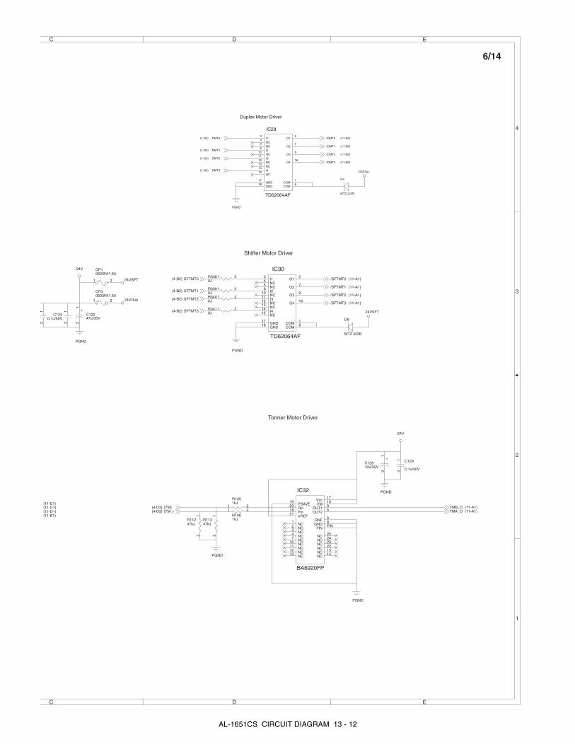
D5
MTZ J22B
R11347kJ
21
R11247kJ
21
C12810u/35V
12
+
IC28
TD62064AF
I13
NC4
NC5
I26
NC10
I311
NC12
NC13
GND17
O12
O27
O39
O416
COM1
COM8
GND18
I414
NC15
R1051kJ
21
R1061kJ
21
IC32
BA6920FP
Vcc 17
GND 8
Rin20
Fin18 OUT1 9
OUT2 5
VM16
VREF21
RNF6
PSAVE19
NC1
NC2
NC3
NC4
NC7
NC10
NC11
NC12
NC13 NC 14NC 15NC22NC 23NC 24NC 25
FIN FIN
C129
0.1u/50V
12
D6
MTZ J22B
IC30
TD62064AF
I13
NC4
NC5
I26
NC10
I311
NC12
NC13
GND17
O12
O2 7
O39
O4 16
COM1
COM8
GND18
I414
NC1512
CP30603FA1.5A
1 2
C1240.1u/50V
12
C12247u/35V
12
+
CP10603FA1.5A
1 2R3380J
21
R3390J
21
R3400J
21
R3410J
21
PGND
24V
PGND
PGND
PGND
PGND
24VSFT
24VDup
PGND
24V
24VSFT
24VDup
DMT0 /DMT0
DMT1
DMT2
DMT3
/DMT1
/DMT2
/DMT3
(TM)(TM_)
TMB_OTMA_O
SFTMT0 /SFTMT0
SFTMT1
SFTMT2
/SFTMT1
/SFTMT2
/SFTMT3
SFTMT3
(11-D1)(11-D1)
(11-E1)
(11-E1)
(11-B3)
(11-B3)
(11-B3)
(11-B3)
(1-D3)
(1-D3)
(1-D3)
(1-D3)
(4-D3)(4-D3)
(11-A1)(11-A1)
Duplex Motor Driver
Shifter Motor Driver
Tonner Motor Driver
(4-B2)
(4-B2)
(4-B2)
(4-B2)
(11-A1)
(11-A1)
(11-A1)
(11-A1)
C D E
C D E
4
3
2
1
6/14
AL-1651CS CIRCUIT DIAGRAM 13 - 12
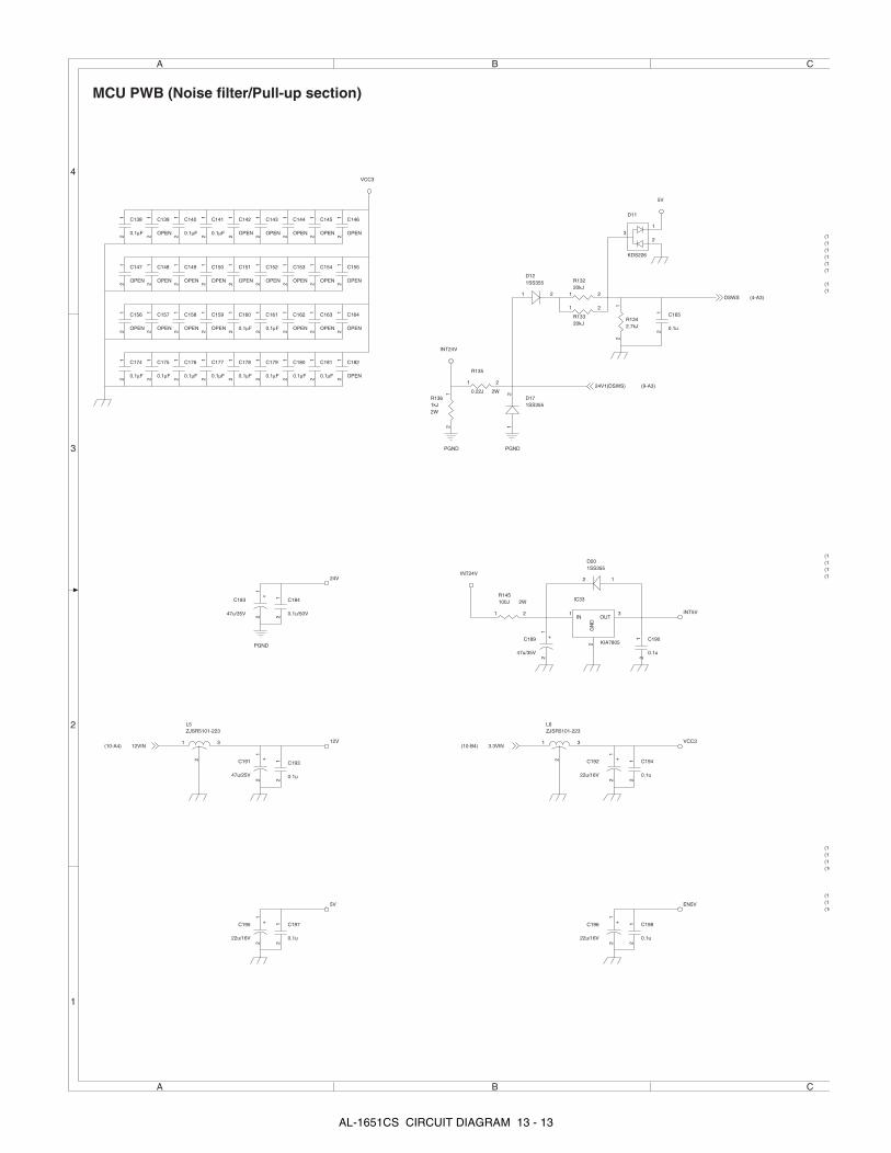
C138
0.1µF
12
C139
OPEN
12
C140
0.1µF
12
C141
0.1µF
12
C142
OPEN1
2
C195
22u/16V
12
+ C197
0.1u
12
D121SS355
1 2
D171SS355
12
R13220kJ
21
R13320kJ
21
R1342.7kJ
21
C165
0.1u
12
C143
OPEN
12
C144
OPEN
12
C145
OPEN
12
C146
OPEN
12
C147
OPEN
12
C148
OPEN
12
C149
OPEN
12
C150
OPEN
12
C151
OPEN
12
C152
OPEN
12
C153
OPEN1
2
C154
OPEN
12
C155
OPEN
12
C156
OPEN
12
C157
OPEN
12
C158
OPEN
12
C159
OPEN
12
C160
0.1µF
12
C161
0.1µF
12
C162
OPEN
12
C163
OPEN
12
C164
OPEN
12
C174
0.1µF
12
C175
0.1µF
12
C176
0.1µF
12
C177
0.1µF
12
C178
0.1µF
12
C179
0.1µF
12
C180
0.1µF
12
C181
0.1µF
12
C182
OPEN
12
R135
0.22J 2W
21
R1361kJ2W
21
C183
47u/35V
12
+C184
0.1u/50V
12
R145100J 2W
21
D201SS355
12
IC33
KIA7805
IN1
GN
D2
OUT3
C190
0.1u
12
C189
47u/35V
12
+
C198
0.1u
12
C196
22u/16V
12
+
C194
0.1u
12
L6ZJSR5101-223
1
2
3
C192
22u/16V
12
+C193
0.1u
12
L5ZJSR5101-223
1
2
3
C191
47u/25V
12
+
D11
KDS226
2
13
5V
PGNDPGND
INT24V
VCC3
24V
PGND
INT24V
INT5V
EN5V
VCC3
5V
12V
DSWS
24V1(DSWS)
3.3VIN12VIN
(9-A3)
(4-A3)
(11(11(11(11
(11
(11(11
(11(11
(11(11
(11
(11(11
(10
(10
(10-B4)(10-A4)
(11(11
(11
A B C
A B C
4
3
2
1
MCU PWB (Noise filter/Pull-up section)
AL-1651CS CIRCUIT DIAGRAM 13 - 13

R12239kJ
21
C171
1000p
12
R130 1kJ21R131 1kJ21
R13710kJ
21
R13810kJ
21
R13939kJ
21
R14010kJ
21
C185
1000p
12
C186
1000p
12
C187
1000p
12
C188
1000p
12
C199
1000p
12
R14639kJ
21
R1487.5kJ
21
R1497.5kJ
21
R1507.5kJ
21
R127 1kJ21
R142 1kJ21R143 1kJ21R144 1kJ21
R141 1kJ21
R14739kJ
21
C200
1000p
12
C202
1000p
12
C201
1000p
12
R12110kJ
21
C173
1000p
12
R125 1kJ21R126 1kJ21
C172
1000p
12
R128 1kJ21
R12310kJ
21
R129 1kJ21
R124 1kJ21
C168
1000p
12
C169
1000p
12
C170
1000p
12
R1194.7kJ
21
R12010kJ
21
R11810kJ
21
R11710kJ
21
R11610kJ
21
C167
1000p
12
C166
1000p
12
R158 1kJ21R159 1kJ21
R157 1kJ21
C203
1000p
12
C204
1000p
12
R154 1kJ21R153 1kJ21
R156 1kJ21R155 1kJ21
R1523.3kJ
21
R15110kJ
21
D7
KDS226
2
13
D8
KDS226
2
13
D14
KDS226
2
13
D15
KDS226
2
13
D16
KDS226
2
13
D18
KDS226
2
13
D19
KDS226
2
13
D21
KDS226
2
13
D22
KDS226
2
13
D23
KDS226
2
13
D24
KDS226
2
13
D27
KDS226
2
13
D28
KDS226
2
13
D25
KDS226
2
13
D26
KDS226
2
13
D29
KDS226
2
13
D9
KDS226
2
13
D10
KDS226
2
13
D13
KDS226
2
13
5V
5V
5V
5V
5V
5V VCC3
VCC3
SB4D
PODPMRDY
(SDSW)
(SB4D)
(POD)(PMRDY)
TCSMFD
MMLD
DVS1
(MMLD)
(TCS)(MFD)
DRST
PSWSPPD
(PPD3)
DVSEL
(SPID)
(PPD2)
(DRST)
(SPPD)
(CED1)CED2
(PSW)
PPD1
CED1(CED2)
PPD2(PPD1)
PD1PD2
(PD1)(PD2)
SDSWSPID
PPD3
(11-D1)(11-E1)(11-E1)(11-D2)
(11-A2)
(11-C3)(11-C3)
(11-A4)(11-C1)
(11-C1)(11-C2)
(11-D1)
(11-D2)(11-B4)
(10-E4)
(10-E4)
(4-A3)(11-E1)(4-A3)(4-A4)
(4-A4)(4-A4)
(4-A4)(4-A4)(4-A4)(4-A3)
(1-D2)
(4-A4)
(4-A4)(4-A3)
(1-D2)
(4-A4)
(4-A4)
(11-B1)(11-D2)
(11-C2)
(4-A3)(4-A3)
D E
D E
4
3
2
1
7/14
AL-1651CS CIRCUIT DIAGRAM 13 - 14
R2251
BR69 150JX41234 5
678
C2830.1U
12
R235 4.7KJ1 2
C2840.1U
12
C2940.1U
12
R232
10kJ
12
12
C2860.1U
12
C2930.1U
12
C2750.1U
12
C2740.1U
12
C2601U
12
C30012P
1 2
R236 4.7KJ1 2
C2780.1U
12
R233 OPEN1 2
C2631U
12
C2920.1U
12
R218 33J1 2
BR77 1234 5
678
12
C2960.1U
12
R231
7.5kF
12
C267NC
12
R2261
C2770.1U
12
R234 OPEN1 2
BR71 150JX41234 5
678
R237 0J1 2
C2760.1U
12
C2730.1U
12
BR70 150JX41234 5
678
C2620.01U
12
C2950.1U
12
C2970.1U
12
X416.1511MHz
12
C2870.1U
12
BR73 33JX41234 5
678
C2590.01U
12
BR72 150JX41234 5
678
12
BR78 1234 5
678
C30612P
1 2
C2880.1U
12
C2850.1U
12
BR38 33J
1234
8765
BR36 33J
1234
8765
BR75 1234 5
678
BR74 1234 5
678
R244 10KJ12
R241 10KJ12
R243 10KJ12R242 10KJ12
R240 10KJ12
IC37
OA-982
GP_C0/PB_ADDR0199
GP_C1/PB_ADDR1201
GP_C2/PB_ADDR2202
GP_C3/PB_ADDR3203
GP_C4/PB_ADDR4204
GP_C5/PB_ADDR5205
GP_C6/PB_ADDR6207
GP_C7/PB_ADDR7208
REG_A9/PB_NCS1178
REG_A8/PB_NCS2180
GP_A126
GP_A2/DC_CHY128
GP_A3/DC_CHX129
GP_A4/DC_PWM130
GP_A5/DC_CHY031
GP_A6/DC_CHX032
GP_A024
GP_A7/DC_PWM034
GP_B0/USART0_TX1
GP_B1/USART0_RX2
GP_B2/USART0_CK8
GP_B3/ANA_SD19
GP_B4/DT_ACKB11
GP_B5/DT_REQB12
GP_B6/DT_ACKA13
GP_B7/DT_REQA14
GP_D0/ADC_A015
GP_D1/ADC_A116
GP_D2/ADC_A219
GP_D3/ADC_CLK21
REG_AD0/PB_DATA0189
REG_AD1/PB_DATA1188
REG_AD2/PB_DATA2187
REG_AD3/PB_DATA3186
REG_AD4/PB_DATA4185
REG_AD5/PB_DATA5183
REG_AD6/PB_DATA6182
REG_AD7/PB_DATA7181
REG_ADDR_VALID/PB_NCS0190
REG_RD_L/PB_NCS3194
REG_WR_L/PB_NAE0195
REG_CS_L/PB_NAE1196
REG_RDY/PB_NWE197
VSS_CORE191
VSS_IO150
VSS_CORE173
VSS_IO136
VSS_CORE121
VSS_IO123
VSS_CORE139
VSS_CORE87
VSS_IO108
VSS_CORE69
VSS_IO98
VSS_CORE35
VSS_IO86
VSS_CORE17
VSS_IO76
VSS_IO64
VSS_IO54
VSS_IO206
VSS_IO41
VSS_IO193
VSS_IO27
VSS_IO10
VSS_IO179
VSS_IO164
INTERRUPT_L/PB_NOE198
RESET_L112
TCK114
TMS116
TDI117
TDO113
BASE_CLK/GP_PWM1168
MAIN_CLK/GP_PWM0170
CLK_EXT/GP_PWM2169
TEST_MODE0172
XIN5
XOUT4
PP_HIDRIVE/USART1_RX143
PP_DRIVE/USART1_TX145
PP_NINIT146
PP_NFAULT147
PP_NSELECTIN151
PP_NAUTOFD152
PP_SELECT153
PP_PERROR154
PP_BUSY155
PP_NACK156
PP_DATA7157
PP_DATA6159
PP_DATA5160
PP_DATA4161
PP_DATA3162
PP_DATA2163
PP_DATA1/USART1_CK165
PP_DATA0166
PP_NSTROBE167
PO_LINE_SYNC/ANA_SCLK37
PO_PAGE_SYNC/ANA_NCS38
PO_REQ/ANA_SD039
PO_ACK/PDATA0/PDS040
PO_DONE/PDATA2/PDS242
PO_WR/PDATA1/PDS143
PO_DATA7/LHEAT/PAS_M44
PO_DATA6/LCTRL/CFIRE245
PO_DATA5/AGATE/CFIRE147
PO_DATA4/ACLK/MFIRE248
PO_DATA3/PENABLE/MFIRE149
PO_DATA2/PLOAD50
PO_DATA1/PCLK51
PO_DATA0/PDATA3/PAS_C52
PI_LINE_SYNC/GP_D6119
PI_TR_TGEN120
PI_TGEN6124
PI_TGEN5125
PI_TGEN4126
PI_TGEN3127
PI_TGEN2128
PI_TGEN1129
PI_TGEN0131
PI_DATA7132
PI_DATA6133
PI_DATA5134
PI_DATA4135
PI_DATA3137
PI_DATA2138
PI_DATA1141
PI_DATA0142
SDRAM_DATA1553
SDRAM_DATA1455
SDRAM_DATA1356
SDRAM_DATA1257
SDRAM_DATA1158
SDRAM_DATA1060
SDRAM_DATA961
SDRAM_DATA862
SDRAM_DATA763
SDRAM_DATA665
SDRAM_DATA566
SDRAM_DATA467
SDRAM_DATA368
SDRAM_DATA272
SDRAM_DATA173
SDRAM_DATA074
ROM_CS_L75
SDRAM_CS1B_L77
SDRAM_CKE78
SDRAM_CLK79
SDRAM_ADDR1182
SDRAM_BANK183
SDRAM_BANK084
SDRAM_ADDR1085
SDRAM_ADDR989
SDRAM_ADDR890
SDRAM_ADDR791
SDRAM_ADDR692
SDRAM_ADDR594
SDRAM_ADDR495
SDRAM_ADDR396
SDRAM_ADDR297
SDRAM_ADDR199
SDRAM_ADDR0100
SDRAM_RAS_L101
SDRAM_CS1A_L102
SDRAM_CS0_L104
SDRAM_DQMB1105
SDRAM_DQMA1106
SDRAM_DQMB0107
SDRAM_DQMA0109
SDRAM_CAS_L110
SDRAM_WE_L111
VDD_IO144
VDD_CORE192
VDD_IO130
VDD_CORE174
VDD_IO115
VDD_CORE140
VDD_IO103
VDD_CORE122
VDD_IO93
VDD_CORE88
VDD_IO81
VDD_CORE70
VDD_IO71
VDD_CORE36
VDD_IO59
VDD_CORE18
VDD_IO46
VDD_IO200
VDD_IO33
VDD_IO184
VDD_IO20
VDD_IO171
VDD_IO3
VDD_IO158
PLLCS_VDDA7
PLLCS_VSSA6
SDRAM_ADDR1280
USB_DP176
USB_DM175
PLLSS_VDDA149
PLLSS_VSSA148
TEST_MODE1177
TRST_L118
GP_D4/ADC_DATA22
GP_D5/ADC_NCS23
VDD_IO25
R320 10KJ12
BR111 33JX41234 5
678
BR112 33JX41234 5
678
BR113 33JX41234 5
678
BR114 33JX41234 5
678
R332 33J1 2
R333 33J1 2R334 33J1 2R335 33J1 2
SDRAM_DATA0
SDRAM_DATA5
_SDRAM_DQMA0
SDRAM_DQMA1
SDRAM_DATA11
_SDRAM_DQMB1
SDRAM_DATA10
SDRAM_CKE
XOUT
SDRAM_DATA6
SDRA
SDRAM_DATA15
SDRAM_DATA9
SDRAM_CS0_L
_SDRAM_DQMA1_SDRAM_DQMB0SDRAM_DQMB0
SDRAM_DQMA0
SDRAM_DATA8
SDRAM_DATA12
SDRAM_DATA14
SDRAM_DATA3SDRAM_DATA2
SDRAM_DATA4
SDRAM_DATA7
SDRAM_DATA13
SDRAM_DQMB1
_SDRAM_CS0_L
SDRAM_DATA1
TRST_L
TCKTMS
XIN
SDRA
SD
TDI
CLK_EXT
PB_ADDR3
PB_ADDR0
PB_ADDR6
PB_ADDR1
PB_ADDR4
PB_ADDR7
PB_ADDR5
PB_ADDR2
_SDRAM_DATA6
_SDRAM_DATA12
_SDRAM_DATA8
_SDRAM_DATA5
_SDRAM_DATA11_SDRAM_DATA10
_SDRAM_DATA13
_SDRAM_DATA2
_SDRAM_DATA14
_SDRAM_DATA9
_SDRAM_DATA0
_SDRAM_DATA7
_SDRAM_DATA4_SDRAM_DATA3
_SDRAM_DATA1
_SDRAM_DATA15
TDO
PODATA7PODATA6PODATA5PODATA4PODATA3PODATA2PODATA1PODATA0
PB_DATA4
PB_DATA1PB_DATA0
PB_DATA5PB_DATA6PB_DATA7
PB_DATA2PB_DATA3
TRST_LTDI
TMSTCKTDO
PIDATA1PIDATA0
PIDATA2
PIDATA4
RY_BY
PIDATA6PIDATA7
PIDATA3
PIDATA5
SDRAM_ADDR11
SDRAM_ADDR3
SDRAM_ADDR8
SDRAM_ADDR12
SDRAM_ADDR0SDRAM_ADDR1
SDRAM_ADDR9
SDRAM_ADDR2
SDRAM_ADDR5SDRAM_ADDR6
SDRAM_ADDR10
SDRAM_ADDR7
SDRAM_ADDR4
/FPOFF
/FPOFF
SDRAM_BANK0SDRAM_BANK1
OA3.3V
OA3.3V
OA3.3V
VCC3
VCC3
/POACK
CLK_EXT
/POREQ
/SC_LINE
CLK_EXT
ES_CMDESS_TS
DT_REQBDT_ACKB
PB_DATA[7:0]PB_NCS1
PB_ADDR[7:0]
PB_NCS3PB_NAE0
PB_NOEPB_NWE
/PR_LINE
/ES_PAGE
/IMC_READY
/ESC_RDY
INT_USBD
WAKEUP
SUSPEND
USBVBUS
(FW)
/H_SYNC
/ESS_RDY
PODATA[7..0]
MDM_IRQ
PIDATA[7..0] /PIREQ
/PIACK
/PIWR
TCKTMSTDI
TRST_L
/FPOFF
MODEM_IN
OA_TX
OA_RX
(/ASIC_RST)TDO
(2-D3)
(2-D3)
(2-D3)(2-D4)
(8-C1)
(13-C3)(13-C4)(9-B3)(9-B3)
(9-A2)(9-A2) (13-C3)
(9-B2)(9-B2)
(13-C3)(13-C3)
(9-B3) (13-C4)
(1-B3)(1-B3)
(1-D2)(9-B2)(9-B2)
(1-A3)(1-B3)(1-B3)(9-D3)
(2-D2)(13-C3)(9-D3)
(2-E3)(9-B2)(2-E3)
(2-D4)
(2-D3)(2-D3)
(2-E3)
(9-B2)(2-C1)(1-B1)
(8-A3)
33JX4
33JX4
33JX4
33JX4
A B C
A B C
4
3
2
1
MCU PWB (IMC2 section 1/2)
AL-1651CS CIRCUIT DIAGRAM 13 - 15

C2690.1U
12
25 33J1 2
C2700.1U
12
C2570.1U
12
R2384.7KJ
1 2
C2800.1U
12
C2990.1U
12
C2790.1U
12
C2680.1U
12
C2780.1U
C2810.1U
12
C2980.1U
12
26 4.7KJ1 2
C2710.1U
12
C2970.1U
C2900.1U
12
C2890.1U
12
C2880.1U
IC38
GND 27GND 46
VCC 37
IO0 29
IO1 31
IO2 33
IO3 35
IO4 38
IO5 40
IO6 42
IO7 44
IO8 30
IO9 32
IO10 34
IO11 36
IO12 39
IO13 41
IO14 43
IO15/A-1 45
A025
A124
A223
A322
A421
A520
A619
A718
A88
A97
A106
A115
A124
A133
A142
A151
A1648
A1717
A1816
VCCW 13
WE11
RESET12
BYTE47
CE26OE28
RY/BYRY/15
A199
A2010
WP/ACC14
C3320.1U
12
C3330.1U
12
C3340.1U
12
C27247U/16V
12
+
R217
0J
12
L10ZJSR5101-102TA
1
2
3
IC39
K4S561632D
VSS 54
RAS18
WE16
CAS17
VSS 41
VSS 28
VDD 1VDD 14VDD 27
BA020
BA121
A023
A124
A225
A326
A429
A530
A631
A732
A833
A934
A1022
A1135
VDDQ 3VDDQ 9VDDQ 43VDDQ 49
VSSQ 6VSSQ 12VSSQ 46VSSQ 52
DQ0 2
DQ1 4
DQ2 5
DQ3 7
DQ4 8
DQ5 10
DQ6 11
DQ7 13
DQ8 42
DQ9 44
DQ10 45
DQ11 47
DQ12 48
DQ13 50
DQ14 51
DQ15 53
LDQM15
UDQM39
CS19
CLK38
CKE37
A1236
N.C40
C26547pF
1 2
C264NM
1 2
C256NM
12
1 21 2
R329
10kJ1
2
1 2
BR115 10kJX41234 5
678
BR116 10kJX41234 5
678
BR117 10kJX41234 5
678
BR118 10kJX41234 5
678
_SDRAM_CLK
_DQMA0
_SDRAM_CKE
_SDRAM_DQMB1_SDRAM_DQMB0
ROM_CS_L
_DQMB1SDRAM_RAS_L
SDRAM_CAS_L
SDRAM_CAS_L
ROM_CS_L
_DQMA1
_SDRAM_DQMA1
_DQMB0SDRAM_WE_L
_SDRAM_DQMA0
SDRAM_BANK0SDRAM_BANK1
M_CS0_L
SDRAM_RAS_L
SDRAM_WE_L
SDRAM_RAS_LSDRAM_CAS_L
_SDRAM_CLK
SDRAM_BANK0
_SDRAM_DQMA0
SDRAM_BANK1
_SDRAM_CS0_LSDRAM_WE_L
_SDRAM_CKE
T
_SDRAM_DATA7
_DATA6
_SDRAM_DATA2
_DATA12
_SDRAM_DATA8
_DATA8
_SDRAM_DATA1
_DATA5
_DATA11
_SDRAM_DATA0
_DATA10
_DATA13
_DATA2
_DATA14
_SDRAM_DATA7
_DATA9
M_DATA0
_DATA7
_DATA4
_SDRAM_DATA3
_SDRAM_DATA4_SDRAM_DATA5
_DATA3
_SDRAM_DATA5
_SDRAM_DATA9
_SDRAM_DATA6
_SDRAM_DATA3
_SDRAM_DATA4
_SDRAM_DATA1
_SDRAM_DATA6
_DATA1
_SDRAM_DATA2
_SDRAM_DATA0
_DATA15
RY_BY
SDRAM_ADDR12
SDRAM_ADDR6
SDRAM_ADDR0
SDRAM_ADDR9
SDRAM_ADDR2
SDRAM_ADDR4
SDRAM_ADDR0
SDRAM_ADDR10
SDRAM_ADDR1
SDRAM_ADDR2
SDRAM_ADDR9
SDRAM_ADDR11
SDRAM_ADDR7
SDRAM_ADDR5
SDRAM_ADDR12
SDRAM_ADDR4SDRAM_ADDR5
SDRAM_ADDR3
SDRAM_ADDR6
SDRAM_ADDR11
SDRAM_ADDR3
SDRAM_ADDR7
SDRAM_ADDR8
SDRAM_ADDR8
SDRAM_ADDR10
SDRAM_ADDR1
_SDRAM_CKE
_SDRAM_CS0_L
_SDRAM_DATA8_SDRAM_DATA9_SDRAM_DATA10_SDRAM_DATA11_SDRAM_DATA12_SDRAM_DATA13_SDRAM_DATA14_SDRAM_DATA15
_SDRAM_DQMA1
_SDRAM_DATA0_SDRAM_DATA1_SDRAM_DATA2_SDRAM_DATA3_SDRAM_DATA4_SDRAM_DATA5_SDRAM_DATA6_SDRAM_DATA7_SDRAM_DATA8_SDRAM_DATA9_SDRAM_DATA10_SDRAM_DATA11_SDRAM_DATA12_SDRAM_DATA13_SDRAM_DATA14_SDRAM_DATA15
VCC3
VCC3
VCC3
VCC3OA3.3V
VCC3
VCC3
VCC3
_SDRAM_CLK
_SDRAM_CLK
SDRAM_BANK[1:0]
_SDRAM_DATA[15:0]
SDRAM_BANK[1:0]
_SDRAM_DATA[15:0]
SDRAM_ADDR[12:0] _SDRAM_DATA[15:0]
SDRAM_BANK[1:0]
SDRAM_ADDR[12:0]
SDRAM_ADDR[12:0]
SDRAM_ADDR[12:0]
/RESET0
_SDRAM_DATA[15:0]
Model
E-Sort Model
FAX Model
Vendor/Type
4Mbit
16Mbit LH28F160BJE-BTL90
LH28F400BVE-BL85
Flash ROMFlash ROM
(8-D4) (8-E4) (8-E3)
(8-E4)(8-D2)(8-D3)(8-C3)
(8-E3)(8-E4)(8-C4)
(8-D2)(8-C3)
(8-C4) (8-D4) (8-E3)
(8-C3) (8-D3) (8-D4)
(8-E4) (8-D3)
(8-D4) (8-D2) (8-D1)
(8-D2)
(8-D4)(8-E4)(8-C3)
(8-D4)(8-C3)
(8-C3)
(8-C4) (8-D4) (8-E4)
LH28F800BJE-PBTL908Mbit(US)FAX Model
(except US)R327/R328/R330 ; 0J
R327/R328/R330 ; OPEN
R327/R328/R330 ; OPEN
(8-D4)
R327 0JR328 0J
R330 0J
C D E
C D E
4
3
2
1
8/14
AL-1651CS CIRCUIT DIAGRAM 13 - 16
C3280.1U
R305 NM
C3260.1U
C320
10U/16V
+
C3150.01U
C3170.01U
L12
MLF1608-J
R304
0J
C3190.01U
C3250.1U
C3270.1U
C3160.01U
C3140.01U
C3180.01U
C3230.1U
C3240.1U
R303
NM
IC43
NC7S04M5X
2 4
1
IC41
ISP1581
/RESET10
EOT11
DREQ12
DACK13
/CS25
/RD26
/WR27
INT28
ALE29
AD030
AD131
AD232
AD333
AD434
AD535
AD638
AD739
DATA040
DATA141
DATA244
DATA345
DATA446
DATA547
DATA648
DATA749
DATA850
DATA951
DATA1052
DATA1153
DATA1254
DATA1355
DATA1456
DATA1557
VC
C(5
.0)
2
VC
C(5
.0)
37
VC
C(5
.0)
43
VC
C(5
.0)
64
VC
C(3
.3)
24
VC
C(3
.3)
58
DG
ND
1
DG
ND
36
DG
ND
42
DG
ND
61
AG
ND
3 23
C3380.1U
C3390.1U
IC42
NC7S08M5X
1
24
PB_DATA1
PB_ADDR5
PB_DATA2
PB_ADDR3
PB_DATA5
PB_DATA1
PB_DATA0
PB_NWE
PB_ADDR2
PB_DATA3PB_DATA4
PB_NOE
PB_DATA5
PB_DATA2
PB_ADDR7
PB_ADDR0
PB_DATA4
PB_DATA0
PB_ADDR1
PB_DATA7
PB_DATA7
PB_DATA3
PB_ADDR6
PB_DATA6
PB_ADDR4
PB_DATA6
AG
VCC3
VCC3
VCC3
AG
VCC3
VCC3
VCC3
PB_DATA[7:0]
PB_NWE
DT_REQB
PB_DATA[7:0]
DT_ACKB
/ASIC_RST
INT_USBD
PB_NCS3
PB_NOE
PB_ADDR[7:0]
PB_NAE0
GND
GND
GND
GND
GND GND
GND
GND
GND
(13-C4)(9-B3)(8-A3)
(13-C4)(9-B3)(8-A3)
(13-C4)(9-B3)
(8-A2)(2-C1)(1-B1)
(8-A2)(8-A2)(8-A2)(8-A3)(8-A3)
(13-C3)(13-C3)
(8-A3)
(13-C3)(8-A3)
A B
A B
4
3
2
1
MCU PWB (IMC2 USB2.0 section 2/2)
AL-1651CS CIRCUIT DIAGRAM 13 - 17
R28
110
KJ
R302
12KF
R28
4N
C
C329 10P
R28
210
KJ
L14
BLM21PG600SN1
L16
BLM21PG600SN1M
R28
710
KJ
R301 NM
C3210.1U
R28910KJ
C330 10P
R29010KJ
Y112MHz
L13
MLF1608-J
R293
1.5KJ
C322
10U/16V
+
CN33
UBR23(ACON)
-D2
+D3
SHIELD5
GND4
+5V1
C331 0.01U
R28
010
KJ
R286 10KJ
R285 10KJR283 10KJ
R288 NC
L15 DLW21SN900SQ2
1 2
34
Vreg(3.3)4
D-5
D+6
RPU7
RREF8
MODE19
DIOR14
DIOW15
INTRQ16
/CS117
/CS018
BUS_CONF19
MODE020
DA221
READY22
XTAL259
XTAL160
WAKEUP62
SUSPEND63
VC
C(3
.3)
24
VC
C(3
.3)
58A
GN
D3
DG
ND
23
PB_NOEPB_NWE
FG
FGAG
AG
AG
VCC3
USBVBUS
SUSPENDWAKEUP
GND FGND_UD1
GND
USB2.0 DEV1
FGND_UD2AGND_UD2
GND
AGND_UD2
GND GND GND
(8-A2)(8-A2)
(8-A2)
C D E
C D E
4
3
2
1
9/14
AL-1651CS CIRCUIT DIAGRAM 13 - 18

CN1
B24B-PHDSS-B
11
33
55
77
99
1111
1313
1515
1717
1919
2121
2323
22
44
66
88
1010
1212
1414
1616
1818
2020
2222
2424
C208
0.1u/50V
12
C207
0.1u/50V
12
PGND PGND
INT24VINT5V
24V5V
EN5V
/BIAS /TC
/POFF
HLOUT
3.3VIN
/PRFW
/GRIDL
12VIN
/MC
To Power unit
(5-C4)(5-C4)
(5-C4)(5-C4)
(5-C1)
(5-C3) (5-D2)
(7-A2)
(7-B2)
(4-C4)(7-A2)
A B C
A B C
4
3
2
1
MCU PWB (Connector section 1)
AL-1651CS CIRCUIT DIAGRAM 13 - 19
C21
110
00p
12
CN4
B4B-PH-K-R
11
22
33
44
R16010kJ
21
C205
1000p
12
R162 1kJ21
C20
910
00p
12
C21
010
00p
12
CN2
28FE-BT-VK-N
11
22
33
44
55
66
77
88
99
1010
1111
1212
1313
1414
1515
1616
1717
1818
1919
2020
2121
2222
2323
2424
2525
2626
2727
2828
D30
KDS226
2
13
5VEN5V5V
VCC3
KEYIN
OUT_A+
OUT_A-OUT_B+
OUT_B-
(OP_CLK)
(LCDDB4)
PSW
(KEYSC2)
(LCDDB6)
(SELIN1)(OP_DATA)
(OP_LATCH)
(SELIN2)
(LCDE)(LCDRS)
(KEYSC1)
(LCDDB5)
(BZR)
(LCDDB7)(SELIN3)
DRST
(PSL)
(KEYSC3)
To Operational PWB
To Mirror motor
(6-A4)(6-A4)(6-A4)(6-A4)
(4-C4)
C D E
C D E
4
3
2
1
10/14
AL-1651CS CIRCUIT DIAGRAM 13 - 20

CN
16
B3B
-PH
-K-R
11
22
33
CN
19
B3B
-PH
-K-S
11
22
33
C21
8
1000
p
1 2
CN
17
B4B
-PH
-K-S
11
22
33
44
CN
27
B5B
-PH
-K-S
11
22
33
44
55
CN
7
B3B
-PH
-K-M
11
22
33
C21
7
1000
p
1 2
C22
0
1000
p
1 2
C21
9
1000
p
1 2
C2220.1u/50V1 2
C2230.1u/50V1 2
CN
20
B18
B-P
HD
SS
-B
11
33
55
77
99
1111
1313
1515
1717
22
44
66
88
1010
1212
1414
1616
1818
CN
24
B24
B-P
HD
SS
-B
11
33
55
77
99
1111
1313
1515
1717
1919
2121
2323
22
44
66
88
1010
1212
1414
1616
1818
2020
2222
2424
CN
11
B4B
-PH
-K-S
11
22
33
44
CN
15
B2P
-VH
-R
11
22
CN
23
B2P
-VH
11
22
R18
615
0J1/
4W
21
CN
22
B5B
-PH
-K-S
11
22
33
44
55
CN
26
B5B
-PH
-K-R
11
22
33
44
55
B10
B-P
HD
SS
-B
CN
9
11
33
55
77
99
22
44
66
88
1010R17
210
J
21
R17
630
0J21
CN
6
08F
E-B
T-V
K-N
11
22
33
44
55
66
77
88
CN
10
B3B
-PH
-K-S
11
22
33
CN
12
B3B
-PH
-K-E
11
22
33
R18
11k
J2
1
R18
739
0J1/
4W
21
R17
530
0J 21
R17
310
kJ
21
CN
13
B05
B-X
AS
K-1
11
22
33
44
55
CN
5
B4B
-PH
-K-R
11
22
33
44 R
185
390J
1/4W
21
R17
939
0J1/
4W
21
R18
039
0J1/
4W
21
CN
25
B3B
-PH
-K-S
11
22
33
D38
KD
S22
6213
D36
KD
S12
0
2
13
D35
KD
S12
1
2
13
CN
40
10F
LS-S
M1-
TB
11
22
33
44
55
66
77
88
99
1010
PG
ND
PG
ND
PG
ND
PG
ND
INT
24V
24V
24V
24V
24V
M5V
24V
INT
5V
24V
VC
C3
5V
24V
5V
EN
5VE
N5V
24V
24V
SF
T
24V
Dup
24V
5V5V
5V
5V
VC
C3
SP
MT
_0
SD
SW
SP
PD
SB
4DS
PID
SP
MT
_3/S
GS
/SR
RC
/SP
US
SP
MT
_2S
PM
T_1
PO
D
/RR
S
PP
D1
PP
D2
TM
A_O
TM
B_O
TxD
1
MM
LD/M
MD
VF
MO
UT
/VF
MC
NT
24V
1(D
SW
S)
/VID
EO
PM
CLK
_AP
MR
DY
/PM
D
SH
OLD
/SF
TM
T0
/SF
TM
T2
/SF
TM
T3
CE
D1
/LD
EN
/SY
NC
RT
H_I
N
TC
SD
VS
EL
/SP
FS
(SC
L1)
(SD
A1)
/SF
TM
T1
/DM
T0
/DM
T1
/DM
T2
/DM
T3
PD
1
/CP
FS
1
/MP
FS
MF
D
/RE
SE
T0
TD
I
OA
_RX
OA
_TX
TD
OT
MS
TR
ST
_L
TC
K
For
SP
F/D
SP
F M
odel
Onl
y
To M
ain
mot
or
To F
an m
otor
To In
terlo
ck s
witc
h
To L
SU
To C
asse
tte d
etec
t
To C
asse
tte p
aper
sole
noid
To S
hifte
r m
otor
(For
deb
ug)
Not
mou
nted
To T
oner
mot
or
To P
aper
pas
s de
tect
To P
aper
out
det
ect
To H
L un
it
To M
ulti
unit
To S
PF
uni
t
(5-C
1)(7
-C3) (5
-C3)
(5-C
3)
(7-B
3)
(7-C
4)(5
-C1)
(5-C
2)
(5-C
2)(5
-D1)
(4-C
4)
(4-E
1)
(1-D
3)
(6-E
2)(6
-E2)
(7-C
1)
(5-C
3)
(7-C
2)
(7-C
2)
(7-C
3)
(7-C
4)
(7-C
4)
(5-C
3)
(5-C
3)
(5-D
3)
(7-C
4)(7
-C4)
(5-B
2)
(6-C
2)(6
-C2)
(7-C
2)
(5-B
2)(5
-B2)
(5-B
2)
(6-C
2)(6
-C2)
(7-C
3)
To D
V U
nit
with
CR
UM
(7-C
3)
To R
esis
t rol
ler
sole
noid
(4-A
1)(4
-B1)
To D
uple
x m
otor
(6-E
4)
For
CR
UM
Mod
el O
nly
To P
aper
det
ect
(6-E
4)(6
-E4)
(6-E
4)
(6-E
3)(6
-E3)
(6-E
3)(6
-E3)
(7-C
4)
CP
U S
eria
l
OA
982
JTA
G &
Ser
ial
AB
CD
E
AB
CD
E
4 3 2 1
4 3 2 1
MC
U P
WB
(C
on
nec
tor
sect
ion
2)
11/1
4
AL-1651CS CIRCUIT DIAGRAM 13 - 21
R17
74.
7kJ
21
C22
1
1000
p
1 2
CN
14
B3B
-PH
-K-S
11
22
33
R17
81k
J2
1
CN
18
B14
B-P
HD
SS
-B
11
33
55
77
99
1111
1313
22
44
66
88
1010
1212
1414
C2261000p1 2
C2271000p1 2
C2281000p1 2
D37
KD
S22
6
213
R31
815
0J1/
4W
21
CN
8
B3B
-PH
-K-S
11
22
33
PG
ND
5V24
V
5V5V
24V
PP
D3
(SD
OD
)
CE
D2
PD
2
/MC
NT
/CP
FS
2
For
SP
F/D
SP
F M
odel
Onl
y
To C
over
ope
n de
tect
To 2
nd. c
asse
tte
(7-C
4)
(7-C
1)
(5-C
3)
(4-A
3)
(7-C
4)
To M
echa
nica
l CO
UN
TE
R
AB
CD
AB
CD
4 3 2
4 3 2
MC
U P
WB
(C
on
nec
tor
sect
ion
3)
11/1
4
AL-1651CS CIRCUIT DIAGRAM 13 - 22
C24
5
0.1u
C23
5
100p
C24
0
100p
C23
6
100p
R19
63.
3KJ
R20
910
kJ
C24
4
0.1u
C23
7
100p
C24
9
100p
R20
422
J
R19
710
kJ
C24
2
0.1u
R20
010
kJR
198
10kJ
C23
8
100p
C24
1
100p
C24
6
100p
C24
7
330p
C24
3
0.1u
C23
3
100p
C23
4
100p
C23
9
100p
C24
8
100p
BR
9122
J1 2 3 4
8 7 6 5
BR
9022
J1 2 3 4
8 7 6 5
C23
0
100p
CN
28
IEE
E12
84_C
N
D-G
ND
30
D-G
ND
26
HLH
IN35
D-G
ND
27
/INIT
31
D-G
ND
28
SG
16
D-G
ND
29
NC
15
SLC
T13
NC
34
Dat
a 0
2
Dat
a 1
3
FG
17
Dat
a 2
4
D-G
ND
19
Dat
a 3
5
D-G
ND
20
Dat
a 5
7
D-G
ND
21
Dat
a 6
8
D-G
ND
22
/SLC
T IN
36
D-G
ND
23
/AU
TO F
D14
D-G
ND
24
D-G
ND
25
/D S
TB
1
PLH
OU
T18
/AC
K10
BU
SY
11
PE
12
/FA
ULT
32
Dat
a 4
6
Dat
a 7
9
D-G
ND
33
Shield
C22
9
100p
IC34
74LV
X16
1284
HD
1
A9
2
A10
3
A11
4
A12
5
A13
6
Vcc
7
A1
8A
29
GN
D10
A3
11A
412
A5
13A
614
GN
D15
A7
16A
817
Vcc
18
PLH
in19
A14
20
A15
21
A16
22
A17
23
HLH
24H
LHin
25
C17
26C
1627
C15
28C
1429
PLH
30
Vcc
-cab
le31
B8
32
B7
33
GN
D34
B6
35
B5
36
B4
37
B3
38
GN
D39
B2
40
B1
41
Vcc
-cab
le42
Y13
43Y
1244
Y11
45Y
1046
Y9
47
DIR
48
C23
1
100p
C23
2
100p
BR
8922
J1 2 3 4
8 7 6 5
BR
9222
J1 2 3 4
8 7 6 5
D39
11E
QS
06
1 2
CN
39
24F
MN
-BT
K-A
11
22
33
44
55
66
77
88
99
1010
1111
1212
1313
1414
1515
1616
1717
1818
1919
2020
2121
2222
2323
2424
R31
90J
R32
6O
PE
N
/ST
B
PAR
AD
7PA
RA
D6
/INIT
/AC
KB
US
Y
/FA
ULT
PAR
AD
1
SLC
T
PAR
AD
2PA
RA
D3
/RE
V
PAR
AD
4
/SLC
TIN
PAR
AD
5
/AU
TOF
D
PEPA
RA
D0
/ST
B
PAR
AD
7PA
RA
D6
/INIT
/AC
KB
US
Y
/FA
ULT
PAR
AD
1
SLC
T
PAR
AD
2PA
RA
D3
/RE
V
PAR
AD
4
/SLC
TIN
PAR
AD
5
/AU
TOF
D
PEPA
RA
D0
EN
5VV
CC
3
EN
5VV
CC
3
EN
5V
VC
C3
EN
5V
/INIT
/AC
K
/AU
TOF
D/S
TB
PAR
AD
[7..0
]
/RE
V
BU
SY
/FA
ULT
/SLC
TINPE
SLC
T
(/A
SIC
_RS
T)
(2-D
2)
(2-E
2)
3.3V
5V
IEE
E12
84 C
onne
ctor
F.G
IEE
E12
84 D
river
/Rec
eive
r
(2-D
2)(2
-D2)
(2-D
2)(2
-D2)
(2-D
2)
(2-D
2)(2
-D2)
(2-D
2)(2
-D2)
To N
IC P
WB
AB
CD
E
AB
CD
E
4 3 2 1
4 3 2 1
MC
U P
WB
(IE
EE
1284
Inte
rfac
e se
ctio
n)
12/1
4
AL-1651CS CIRCUIT DIAGRAM 13 - 23
R30
610
kJ
21
CN
38
20F
E-B
T-V
K-N
11
22
33
44
55
66
77
88
99
1010
1111
1212
1313
1414
1515
1616
1717
1818
1919
2020
CN
37
26F
E-B
T-V
K-N
11
22
33
44
55
66
77
88
99
1010
1111
1212
1313
1414
1515
1616
1717
1818
1919
2020
2121
2222
2323
2424
2525
2626
C359OPEN
1 2
C360OPEN
1 2
C361OPEN
1 2
C362OPEN
1 2
C363OPEN
1 2
C364OPEN
1 2
C365OPEN
1 2
C366OPEN
1 2
C367OPEN
1 2
C368OPEN
1 2
C369OPEN
1 2
C370OPEN
1 2
C371OPEN
1 2
C372OPEN
1 2
C373OPEN
1 2
C374OPEN
1 2
C375OPEN
1 2
C376OPEN
1 2
PB
_AD
DR
7
PB
_AD
DR
3P
B_A
DD
R2
PB
_AD
DR
0
PB
_AD
DR
5P
B_A
DD
R6
PB
_AD
DR
1
PB
_AD
DR
4PB
_DAT
A7
PB
_DAT
A3
PB
_DAT
A0
PB
_DAT
A1
PB
_DAT
A4
PB
_DAT
A6
PB
_DAT
A5
PB
_DAT
A2
MD
M_I
RQ
MS
U_S
T1
D1
D0
D4
D7
D2
D3
D5
D6
PB
_DAT
A7
PB
_DAT
A3
PB
_DAT
A0
PB
_DAT
A1
PB
_DAT
A4
PB
_DAT
A6
PB
_DAT
A5
PB
_DAT
A2
MD
M_I
RQ
D1
D0
D4
D7
D2
D3
D5
D6 MS
U_S
T1
VC
C3
24V
PG
ND
EN
5V
VC
C3
/RD
/CS
4M
SU
_ST
1
MD
M_I
RQ
PB
_AD
DR
[7:0
]
PB
_NA
E0
PB
_NC
S1
PB
_NO
EP
B_N
WE
(/A
SIC
_RS
T)
MO
DE
M_I
N
PB
_DAT
A[7
:0]
D[1
5..0
]
To M
odem
PW
B
To M
odem
PW
B
(9-B
3)(8
-A3)
(8-A
3)(9
-B3)
(9-B
3)
(9-A
2)(8
-A3)
(9-B
2)(4
-D3)
(8-A
3)
(8-A
3)(8
-A3)
(8-A
2)
(9-B
2)
(4-A
2)(2
-A1)
(3-A
1)(1
-D2)
(4-A
3)
(1-D
3)(3
-A2)
(2-C
1)(1
-B3)
(1-A
3)
AB
CD
AB
CD
4 3 2 1
4 3 2 1
MC
U P
WB
(M
od
em I/
F C
on
nec
tor)
13/1
4
AL-1651CS CIRCUIT DIAGRAM 13 - 24

R16
51k
J2
1
R16
410
kJ
21
C21
2
1000
p
1 2
D32
KD
S22
6
213
R16
915
kJ
21
Q5
KT
C31
98
C21
5
0.1u
/50V
1 2
D33
11E
QS
06
12
R16
610
kJ
21
Q4
KT
B11
51 Y
R16
715
kJ
21
R16
85.
6kJ
21
C21
4
47u/
35V
1 2+
R17
056
kJ
21
C21
347
u/35
V
1 2+
CP
406
03FA
1.5A
12
L9 220u
H
TW
KA
-221
K
C21
633
p1
2
CN
3
FF
4-32
-S15
D5
11
33
55
77
99
1111
1313
1515
1717
1919
2121
2323
2525
2727
2929
3131
22
44
66
88
1010
1212
1414
1616
1818
2020
2222
2424
2626
2828
3030
3232
AF
E_D
B4
AF
E_D
B6
AF
E_D
B5
AF
E_D
B7
VC
LV
CL
VC
L
AF
E_D
B2
AF
E_D
B1
AF
E_D
B3
AF
E_D
B0
AF
E_D
B0
AF
E_D
B1
AF
E_D
B2
AF
E_D
B3
AF
E_D
B4
AF
E_D
B5
AF
E_D
B6
AF
E_D
B7
12V
PG
ND
EN
5V
PG
ND
24V
PG
ND
VC
C3
mt_
at_h
ome
CC
D_P
HI1
CC
D_P
HI2
CC
D_C
PC
CD
_RS
CC
D_T
G
CL
BS
AM
P
VS
AM
P
AD
CLK
AF
E_S
EN
AF
E_S
CK
AF
E_S
DI
AF
E_D
B[7
..0]
To S
cann
er u
nit
(1-D
2)
(2-A
4)(2
-A4)
(2-A
4)(2
-A4)
(2-A
4)(1
-D2)
(2-A
4)
1/4W
(2-A
4)
Cop
y La
mp
Inve
rter
AB
CD
E
AB
CD
E
4 3 2 1
4 3 2 1
MC
U P
WB
(S
can
ner
I/F
sec
tio
n)
14/1
4
AL-1651CS CIRCUIT DIAGRAM 13 - 25
2. OPERATION PWB
OP
ER
ATI
ON
PW
B (
LED
/LC
D S
ectio
n)
C332100p
R33
310
0J
R33
410
0J
PM
L
LED
311
R32
60J
C331100p
Q30
5K
RA
225S
3
2
1
C327100pC328100p
C33
3
0.1u
RE
ADY
LED
310
Q30
1
KR
C10
6S
1
2
3
C30
5
1000
p
R33
110
0J
C329100pC330100p
IC30
4
TB
6272
5AF
/OUT27
/OUT38
/OUT49
/OUT510
/OUT611
/OUT16
/OUT05
VCC16
/ENABLE13
/LATCH4
S-IN2
CLOCK3
S-OUT14
GND1
/OUT712
R-EXT15
R30
6O
PE
N
R30
210
0J
PR
INT
LED
303
C32
2
0.1u
R32
50J
R32
810
kJ
R32
782
0J
C30
7
open
R30
147
0J
R32
910
0J
SP
ON
LED
308
R30
410
0J
1CA
S
LED
306
Q30
2
KR
C10
6S
1
2
3
R33
210
0J
C30
8
Ope
n
IC30
1
GP
M18
1C0
GN
D10
V5
9
VD
D8
RS
7
R/W
6
E5
DB
44
DB
53
DB
62
DB
71
R32
40J
2CA
S
LED3
05
Q30
3K
RA
225S
3
2
1
R30
310
0J
CO
PY
LED
304
ALM
LED
307
C32
3
open
FAX
LED
301
Q30
4K
RA
225S
3
2
1
MB
LED
309
R33
010
0J
R335560J
C30
6
1000
p
SC
AN
LED
302
R30
50J
R32
310
KJ
LCD
RS
#
LCD
DB
7#
LCD
DB
4#
LCD
DB
6#
LCD
RS
#
LCD
E#
LCD
E#
LCD
DB
7#
LCD
DB
4#
LCD
DB
6#
LCD
DB
5#LC
DD
B6
LCD
DB
7
LCD
DB
4
LCD
DB
5#
LCD
DB
5
3.3V
5VE
N
3.3V
3.3V
5V
PS
L
LED
_V2
OP
-CLK
OP
-DAT
A
OP
-LAT
CH
LED
_V3
LED
_V1
DAT
A1
LCD
E
LCD
RS
LCD
DB
[7..4
]
Pin
Hol
es x
10
To L
CD
=(1.
15/8
20)x
14.9
=20.
9mA
Iout
=(1.
15/R
ext)
x14.
9 [A
]
1/3
AA
BB
CC
DD
EE
44
33
22
11
AL-1651CS CIRCUIT DIAGRAM 13 - 26
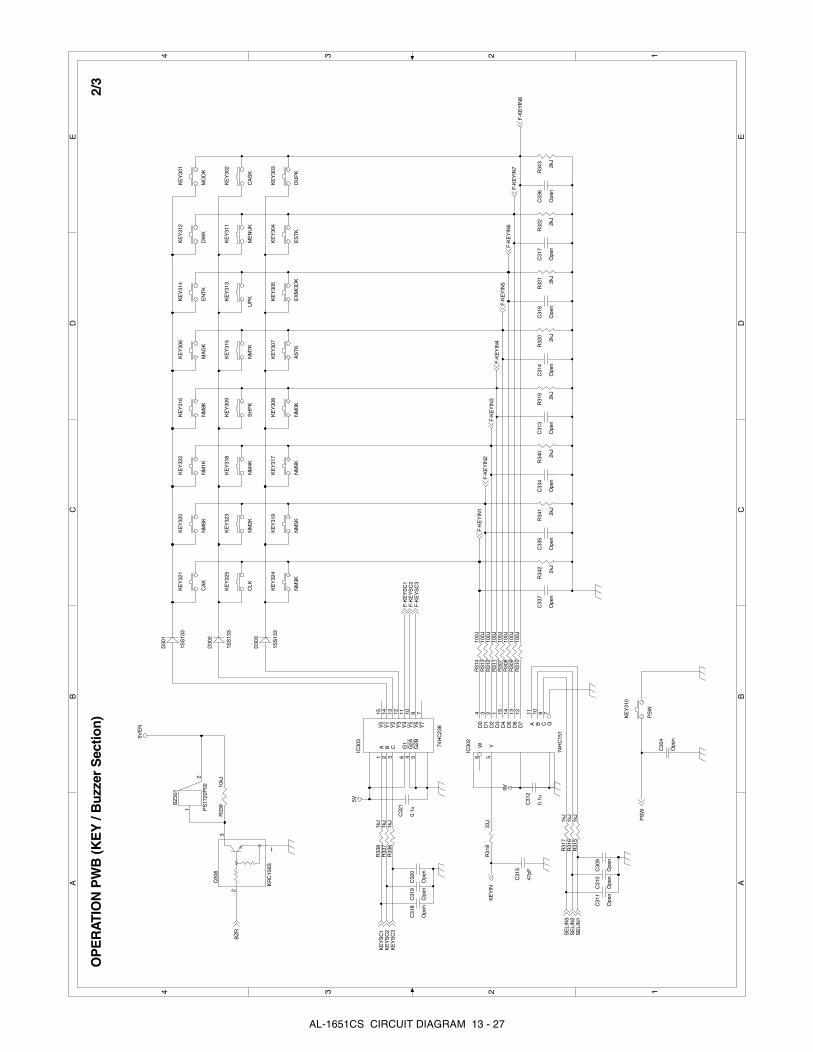
OP
ER
ATI
ON
PW
B (K
EY
/ B
uzze
r S
ectio
n)
R32
2
2kJ
KE
Y31
8
NM
4K
KE
Y32
5
CLK
KE
Y30
9
SH
PK
R32
0
2kJ
C31
7
Ope
n
C32
0
Ope
n
C33
4
Ope
n
D30
1
1SS
133
KE
Y32
3
NM
2K
C31
3
Ope
n
C31
9
Ope
n
Q30
6
KR
C10
6S
1
2
3
C31
8
Ope
n
KE
Y31
0
PS
W
R31
410
0J
KE
Y31
5
NM
7K
C33
6
Ope
n
R31
110
0J
KE
Y31
9
NM
5K
IC30
3
74H
C23
8Y0
15
Y1
14
Y2
13
Y3
12
Y4
11
Y5
10
Y6
9
Y7
7
A1
B2
C3
G2B
5G
2A4
G1
6
KE
Y30
8
NM
0K
R32
1
2kJ
C30
4
Ope
n
KE
Y32
1
CA
K
R33
81k
J
C33
5
Ope
n
R31
833
J
R33
910
kJ
KE
Y30
6
MA
GK
KE
Y32
0
NM
6K
R34
1
2kJ
D30
2
1SS
133
C31
2
0.1u
BZ
301
PS
1720
P02
1
2
R33
71k
J
R34
0
2kJ
C31
5
47pF
KE
Y30
2
CA
SK
R31
9
2kJ
R31
010
0J
KE
Y31
7
NM
9K
R34
3
2kJ
C32
1
0.1u
R33
61k
J
R31
210
0J
C31
6
Ope
n
KE
Y31
6
NM
8K
KE
Y32
4
NM
3K
KE
Y30
3
DU
PK
R31
71k
J
KE
Y30
4
ES
TK
R34
2
2kJ
R30
810
0J
C30
9
Ope
n
C31
0
Ope
n
KE
Y31
3
UP
K
C31
4
Ope
n
R31
310
0J
C31
1
Ope
n
KE
Y32
2
NM
1K
R31
61k
J
KE
Y30
1
MO
DK
IC30
2
74H
C15
1
D0
4
D1
3
D2
2
D3
1
D4
15
D5
14
D6
13
D7
12
A11
B10
C9
G7
W6
Y5
KE
Y31
2
DW
K
C33
7
Ope
n
KE
Y30
7
AS
TK
KE
Y30
5
EX
MO
DK
KE
Y31
1
ME
NU
K
KE
Y31
4
EN
TK
R30
710
0J
R31
51k
J
R30
910
0J
D30
3
1SS
133
5V
5V
5VE
N
KE
YS
C1
KE
YS
C2
KE
YS
C3
KE
YIN
SE
LIN
3S
ELI
N2
SE
LIN
1
PS
W
F-K
EY
SC
2F
-KE
YS
C3
F-K
EY
SC
1
F-K
EY
IN1
F-K
EY
IN2
F-K
EY
IN3
F-K
EY
IN4
F-K
EY
IN5
F-K
EY
IN6
F-K
EY
IN7
F-K
EY
IN8
BZ
R
2/3
AA
BB
CC
DD
EE
44
33
22
11
AL-1651CS CIRCUIT DIAGRAM 13 - 27

OP
ER
ATI
ON
PW
B (
Con
nect
or S
ectio
n)
CN
303
S3B
-PH
-K-S
1 2 3
C30
3
47uF
/16v
C32
4
0.1u
C30
2
47uF
/16v
C30
1
47uF
/16v
CN
301
18F
E-S
T-V
K-N
1 2 3 4 5 6 7 8 9 10 11 12 13 14 15 16 17 18
CN
302
28F
E-S
T-V
K-N
1 2 3 4 5 6 7 8 9 10 11 12 13 14 15 16 17 18 19 20 21 22 23 24 25 26 27 28
C32
5
0.1u
C32
6
0.1u
DR
ST
DR
ST
LCD
DB
4
LCD
DB
7
LCD
DB
5LC
DD
B6
3.3V
5V5V
EN
PS
L
PS
WK
EY
IN
OP
-CLK
OP
-LAT
CH
OP
-DAT
AS
ELI
N1
SE
LIN
2
KE
YS
C2
KE
YS
C3
LED
_V3
F-K
EY
IN1
BZ
RK
EY
SC
1
LCD
RS
LCD
E
SE
LIN
3LC
DD
B[7
..4]
F-K
EY
IN4
DAT
A1
F-K
EY
IN2
F-K
EY
IN8
LED
_V2
F-K
EY
IN5
LED
_V1
F-K
EY
SC
2
F-K
EY
IN6
F-K
EY
SC
3
F-K
EY
SC
1
F-K
EY
IN7
F-K
EY
IN3
To M
CU
PW
B
To D
rum
Initi
al D
etec
tor
To F
AX
Key
PW
B
Clo
se to
CN
1
3/3
AA
BB
CC
DD
EE
44
33
22
11
AL-1651CS CIRCUIT DIAGRAM 13 - 28
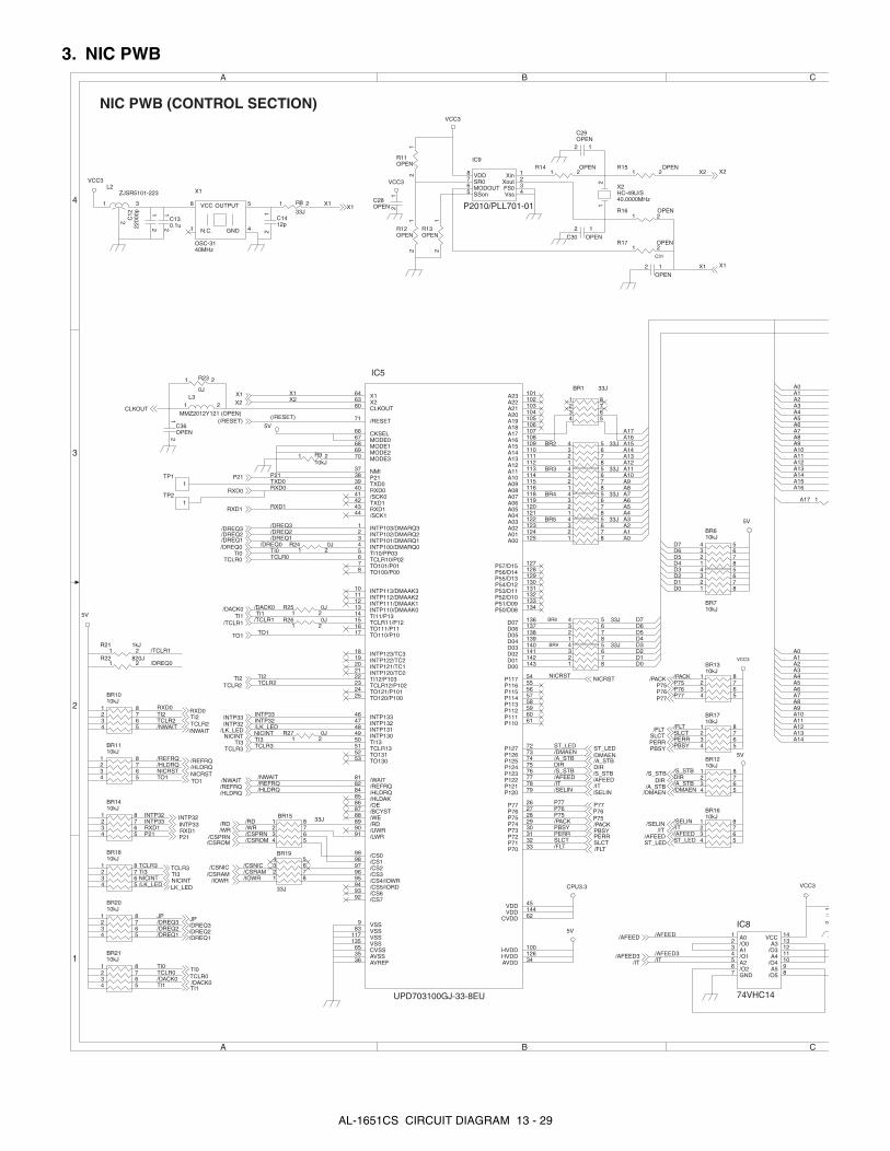
3. NIC PWB
1
R910kJ
21
BR1533J1
234
8765
C130.1u
12
L2ZJSR5101-223
1
2
3
X1
OSC-3140MHz
N.C.1
VCC8 OUTPUT 5
GND 4
C1412p
12
C12
2200
0p 12
R8
33J21
L3
MMZ2012Y121 (OPEN)1 2
IC8
74VHC14
A01
/O02
A13
/O14
A25
/O26
GND7
VCC 14
A3 13
/O3 12
A4 11
/O4 10
A5 9
/O5 8
12
R17 OPEN21
R15 OPEN21
X2HC-49U/S40.0000MHz
12
R16 OPEN21
R14 OPEN21
R13OPEN
21
C31
OPEN12
C30 OPEN12
C29OPEN
12
R12OPEN
21
R11OPEN
21
IC9
P2010/PLL701-01
Xin 1
Xout 2
FS0 3
Vss 4SSon5MODOUT6SR07VDD8
TP11
TP21
BR1310kJ
1234
8765
BR1710kJ
1234
8765
C28OPEN
12
BR2110kJ
1234
8765
BR1410kJ
1234
8765
IC5
UPD703100GJ-33-8EU
/WE88
/RD89
/UWR90
/LWR91
/CS099
/CS198
/CS297
/CS396
TO121/P10124
TO120/P10025
/CS4/IOWR95
/CS5/IORD94
/CS693
/CS792
VSS9
VSS83
VSS117
VSS135
CVSS65
AVSS35
AVREF36
TO13053TO13152TCLR1351TI1350INTP13049INTP13148INTP13247INTP13346
/WAIT81
/REFRQ82
/HLDRQ84
/HLDAK85
/OE86
/BCYST87
INTP120/TC021
TCLR12/P10223TI12/P10322
INTP103/DMARQ31
INTP102/DMARQ22
INTP101/DMARQ13
INTP100/DMARQ04
TI10/PP035
TCLR10/P026
TO101/P017
TO100/P008
INTP113/DMAAK310
INTP112/DMAAK211
INTP111/DMAAK112
INTP110/DMAAK013
TI11/P1314
TCLR11/P1215
TO111/P1116
TO110/P1017
INTP123/TC318
INTP122/TC219
INTP121/TC120
X164
X263
CLKOUT80
/RESET71
CKSEL66
MODE067
MODE168
MODE269
MODE370
NMI37
P2138
TXD039
RXD040
/SCK041
TXD142
RXD143
/SCK144
A08 116A09 115A10 114A11 113A12 112A13 111A14 110A15 109A16 108A17 107A18 106A19 105A20 104A21 103A22 102A23 101
A00 125A01 124
P114 57P115 56
D01 142
P116 55P117 54
D02 141D03 140D04 139D05 138D06 137D07 136
P50/D08 134P51/D09 133P52/D10 132P53/D11 131P54/D12 130P55/D13 129
A02 123A03 122A04 121A05 120A06 119A07 118
P56/D14 128P57/D15 127
P73 30P74 29P75 28P76 27
AVDD 34
P77 26
HVDD 126
P120 79
HVDD 100
P121 78
CVDD 62
P122 77
VDD 144
P123 76
VDD 45
P124 75
P70 33
P126 73
P71 32
P127 72
P72 31
P113 58
P112 59
D00 143
P111 60
P110 61
P125 74
BR1810kJ
1234
8765
BR1110kJ
1234
8765
BR1010kJ
1234
8765
BR1210kJ
1234
8765
BR2010kJ
1234
8765
BR1610kJ
1234
8765
BR19
33J
1234
8765
BR1 33J
1234
8765
BR2 33J
1234
8765
BR3 33J
1234
8765
BR4 33J
1234
8765
BR5 33J
1234
8765
BR610kJ
1234
8765
BR710kJ
1234
8765
BR8 33J
1234
8765
BR9 33J
1234
8765R21 1kJ
21R22 820J
21
R23
0J
21
R24 0J21
R25 0J21
R26 0J21
R27 0J21
C36OPEN
12
/RD/WR
/CSNIC/CSRAM/IOWR
X1
/AFEED
/AFEED3/IT
X2
/PACKP75P76P77
/FLTSLCTPERRPBSY
A11
A4
/HLDRQ
/DREQ0
TI3
A10
A1
A14
A12A11
A11
/SELIN
/PACK
INTP32
TI0
A15
A10A9
A5
ST_LED
TI0
TCLR3
A9 A15
A12
P77
RXD1
X2
TCLR0
A8
A6
DIR
P76
PBSY
(/RESET)
/DREQ3
/NWAIT
TCLR0
A16
A13
/DACK0
/REFRQ
A7
A13
A7
/A_STB
P75
A6
A14
PERRSLCT
TCLR2
/HLDRQ
A17
X1
A8
DIR
A14
A2
/FLT
INTP33
A16A9
TI1
A3
A1
A1A0
TCLR2TI2
/S_STB
NICRST
X1
/TCLR1
A8
A0
A10
TXD0
A0
A17
A7A6
A2
/NWAIT
NICRST
/DMAEN
/AFEED
RXD0
TO1
A13
A5
A5A4
/A_STB
/S_STBTO1
P21
/DREQ2
/LK_LED
A4
A12
A3
A3
/DMAEN
RXD0
/REFRQ
/DREQ1
A2
/IT
TI2
NICINT
/DREQ1/DREQ2/DREQ3JP
ST_LED
/SELIN/IT/AFEED
TI1/DACK0
INTP32INTP33RXD1P21
TCLR3TI3NICINT/LK_LED
/CSPRN/CSROM
/TCLR1
/DREQ0
D7
D4D3
D2
D1D2
D1
D6
D3
D7
D0
D5
D0
D6
D5
D4
CPU3.3
VCC3
VCC3
VCC3
VCC3
VCC3
5V
5V
5V
5V
5V
CLKOUT
X1
X1
X1
X2
X2
(/RESET)
P21
RXD0
RXD1
/DREQ3/DREQ2/DREQ1/DREQ0
TI0TCLR0
/DACK0TI1
/TCLR1
TO1
TI2TCLR2
INTP33INTP32
NICINTTI3
TCLR3
/NWAIT/REFRQ/HLDRQ
/RD/WR
/CSNIC/CSRAM
/IOWR
RXD0TI2TCLR2/NWAIT
/REFRQ/HLDRQNICRSTTO1
TI0TCLR0
/LK_LED
NICRST
ST_LED/DMAEN/A_STBDIR/S_STB/AFEED/IT/SELIN
P77P76P75/PACKPBSYPERRSLCT/FLT
/AFEED
/AFEED3/IT
/S_STBDIR
/A_STB/DMAEN
/PACKP75P76P77
/FLTSLCTPERRPBSY
/DREQ1/DREQ2/DREQ3JP
ST_LED
/SELIN/IT
/AFEED
TI1/DACK0
INTP32INTP33RXD1P21
TCLR3TI3NICINTLK_LED
/CSPRN/CSROM
A B C
A B C
4
3
2
1
NIC PWB (CONTROL SECTION)
AL-1651CS CIRCUIT DIAGRAM 13 - 29
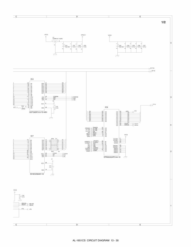
R10
OPEN21
C180.1U
12
L4ZJSR5101-102TA
1
2
3
C1910U/16V
12
+C210.1U
12
C220.1U
12
C230.1U
12
C2010U/16V
12
12
12
12
12
+C240.1U
C250.1U
C270.1U
C260.1U
IC6
GNDIO 30GNDIO 11GNDIO 24
I/O 22
I/O 12
I/O 13
I/O 14
I/O 15
I/O 18
I/O 19
I/O 20
I/O 21
I/O 34
I/O 35
VCCINT 9
VCCINT 17
VCCIO 29
VCCIO 41
GNDINT 16
I/O33
I/O32
I/O31
I/O28
I/O27
I/O26
I/O25
I/O23
I/O43
I/O44
I/O1
IN38
I/O10
I/O8
I/O6
IN39
IN37
IN40
I/O2
GNDIO 4
I/O42
I/O7
I/O3
I/O5
GNDINT 36
C150.1U
12
C160.1U
12
IC7
IO0 11
IO1 12
IO2 13
IO3 15
IO4 16
IO5 17
IO6 18
IO7 19
/CS1 20
/WE 27
/OE 22
VCC 28
VSS 14
A010
A19
A28
A37
A46
A55
A64
A73
A825
A924
A1021
A1123
A122
A1326
A141
IC4
D00 21
D01 22
D02 23
D03 25
D04 26
D05 27
D06 28
D07 29
/CE 30
/WE 7
/OE 32
VCC 8
VSS 24
A020
A119
A218
A317
A416
A515
A614
A713
A83
A92
A1031
A111
A1212
A134
A145
A1511
A1610
NC9
NC6
BR26 33J1234
8765
BR27 33J
1234
8765
/DMAEN/A_STB/S_STBDIR/PACKPBSYDIR3
(/RESET)CLKOUTTO1/RD/WR/CSPRN/DACK0/IOWR
/IT3
/SELIN/SELIN3
P6
P0
P7
P3P4P5
P1P2
/STB
/DREQ0/TCLR1
4
14
1211
11
109
5
15
12
6
16
13
/CSROM
13
7
14
8
2
9
/WR
1
/WR
10
8
0
10
A17
76
/RD
2
/RD
543
/CSRAM
3
D0
D7
D1
D4
D7
D3
D6
D3D4
D1
D0
D5
D2
D6D5
D2
D0D1D2D3D4D5D6D7
VCC3
VCC3 CPU3.3 VCC3
5V
5V
VCC3
/SELIN3/SELIN
/IT3
/CSROM/WR/RD
/CSRAM/WR
/RD
/DMAEN/A_STB/S_STB
DIR/PACKPBSYDIR3
(/RESET)CLKOUT
TO1/RD/WR
/CSPRN/DACK0
/IOWR
/STB
/TCLR1/DREQ0
P[7:0]
D[7:0]
A[17:0]
SST39SF010-70-WH
IS16C256AH-12
EPM3032ATC44-10
C D E
C D E
4
3
2
1
1/2
AL-1651CS CIRCUIT DIAGRAM 13 - 30

R527kJ
21
L1ZJSR5101-102TA
1
2
3
C510U/16V
12
+C60.1U
12
C70.1U
12
C90.1U
12
C80.1U
12
C100.1U
12
C110.1U
12
IC2
IS93C
CS1SK2DI3DO4
IC1
RTL8019AS
INT4100
INT599
RSTDRV33 IOWB30 IORB29 IOCS16B96 IOCHRDY35 AEN34
INT797 INT698
SMEMRB31
SMEMWB32
INT13
INT31 INT22
SA1826
SA1927
SD036
SD137
SD238
SD339
SD440
SD541
SD642
SD743
SD895
SD994
SD1093
SD1192
SD1291
SD1390
SD1488
SD1587
INT04
SA05
SA17
SA28
SA39
SA410
SA511
SA612
SA713
SA815
SA916
SA1018
SA1119
SA1220
SA1321
SA1422
SA1523
SA1624 BD7 77BD6 78BD5 79BD4 80BD3 81BD2 82BD1 84BD0 85
BA21 66BA20 67BA19 68BA18 69BA17 71BA16 72BA15 73BA14 74
TX+ 49RX- 55
GND 28GND 14
VDD 47
VDD 89VDD 70
VDD 17VDD 6
JP 65
X2 51X1 50
LED2 63LED1 62LED0 61LEDBNC 60
TPOUT- 46TPOUT+ 45TPIN- 58
RX+ 56CD- 53CD+ 54
AUI 64
EECS 76BCSB 75
TPIN+ 59TX- 48
GND 44
GND 52
VDD 57
GND 83
GND 86
SA1725
BR24 0J1234
8765
BR25 0J
1234
8765
A0A1A2A3A4
D2D3D4D5D6
NICINT
/WR
/CSNIC/NWAIT
/RD
EESKEEDIEEDO
EECS
/LK_LED
JP
NICRST
D0
D7
D1
5V
ET5V
5V ET5V
5V
CLKOUTNICINT
/CSNIC/NWAIT
/RD/WR
NICRST
JP
LK_LED
D[7:0]
A[17:0]
A B C
A B C
4
3
2
1
NIC PWB (ETHERNET SECTION)
AL-1651CS CIRCUIT DIAGRAM 13 - 31

C10.1U
12
R1820J
21
R3820J
21
R2200J
21
C30.01U
12
C20.01U
12
J1
CON12
12345678
910
1112
CN1
24FMN-SSTK-A
11 22 33 44 55 66 77 88 99 1010 1111 1212 1313 1414 1515 1616 1717 1818 1919 2020 2121 2222 2323 2424
R6 0J
R7OPEN
IC3
NC7S04M5X
2 4
1
R4OPEN
21
C40.1U
12
IC2
IS93C46-3GR
CSSKDIDO GND 5
NC 6NC 7
VCC 8
C340.01U
12
C350.01U
12
L6
TLA-3M103LF
TPOUT+1
CT5
TPRX- 11
TPTXC 7
TPIN-14
TPRXC 10
TPRX+ 9
TPOUT-3 TPTX- 6
TPIN+16
CT12
TPTX+ 8
IC45
NC7WZ17
A11
A23
Y16
Y24
GND2
Vcc5
C37
OPEN
12
C38
0.1u
12
R28OPEN
R29100J
21
/LK_LED
/STB
P7P6
/IT3
/PACKPBSY
/FLT
P1
SLCT
P2P3
DIR3
P4
/SELIN3
P5
/AFEED3
PERR
P0/RESET
/RESET
ST_LED
5V
5V
5VVCC3
5V
5V
P[7:0]
/PACKPBSYPERRSLCT/FLT/STB
/AFEED3/SELIN3
/IT3DIR3
ST_LED
/LK_LED
(/RESET)
10BASE-T
To MCU PWB
C D E
C D E
4
3
2
1
2/2
AL-1651CS CIRCUIT DIAGRAM 13 - 32

4. POWER SUPPLY
A
1 2 3 4 5 6
B
C
D
E
F
G
H
1 2 3 4 5 6
POWER SUPPLY (120V/127V)
AL-1651CS CIRCUIT DIAGRAM 13 - 33
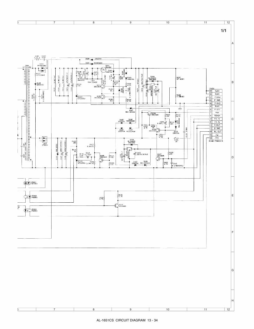
6 7 8 9 10 11 12
6 7 8 9 10 11 12
A
B
C
D
E
F
G
H
1/1
AL-1651CS CIRCUIT DIAGRAM 13 - 34
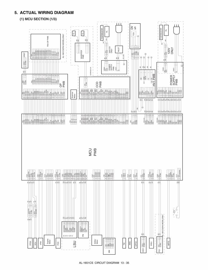
5. ACTUAL WIRING DIAGRAM
P-G
ND
3.3V
IN
7
PO
D
HL
GR
ID
13
TC
GY
OR
GY
WH
/BIA
S/T
C
2
HLN
6 12
PO
D
D-G
ND
15 172
CN
19
24V
P-G
ND
24
OR
GY
RD
BK
24V
P-G
ND
1
HLL
D-G
ND
INT
24V
5
4
PK
/GR
IDL
HLN
N
14
BC
HLO
UT
RD
OR
/PR
L
23
CN
1(1/
2)1
HLL
18 20
LED
PO
D
INT
5V
GY
GY
3
1
TH
ER
MO
STA
T
MC
BIA
S
GY
1 3
LED
PP
D2
PP
D2
D-G
ND
CN
22
12V
IN
FW
PK
PK
GY
LED
PP
D2
PP
D2
D-G
ND
1 2 3
1 2 32
MC
FB
PP
D2
1916
EN
5V
21
5V
22
7
/BIA
S/T
C62
INT
24V
5
/GR
IDL
1IN
T5V
2R
TH
AN
-GN
D1
RT
H2
1R
TH
-IN
AN
-GN
D4 5
PL
CN
101
3O
UT
_B+
4M
otor
OU
T_B
-
OU
T_A
+1
Sca
nner
2O
UT
_A-
CN
4
CC
D-C
P
24
CC
D-R
S
12V
631
CC
D_P
HI1
28 729(A
FE
_DB
4)
CC
D-T
G
VC
L
CC
D_P
HI2
432 1218
(VS
AM
P)
VC
L
916
EN
5V
5
(AD
CLK
)2026
(AF
E_D
B6)
27
D-G
ND
38
(AF
E_D
B1)
MH
PS
CN
3
1014
12V
(AF
E_D
B0)
25(A
FE
_DB
5)
(AF
E_D
B3)
D-G
ND
30(A
FE
_DB
2)
23(A
FE
_DB
7)22
(AF
E_S
CK
)21
D-G
ND
19(A
FE
_SE
N)
17D
-GN
D
15(A
FE
_SD
I)
13(B
SA
MP
)
11D
-GN
D
2P
-GN
D1
P-G
ND
19 28 2924 265 131 7 9 2723 256 21 30171542 83 10 11 12 14 16 18 20 22 31 32
4 8
23 7
11 12
OP
PW
B
1D
RS
T2 6
10
1 5 9
31
LCD
RS
LCD
DB
5LC
DD
B6
KE
YS
C2
LCD
DB
4
SE
LIN
3
KE
YS
C1
D-G
ND
BZ
R
LCD
E
KE
YS
C3
LCD
DB
7
DR
ST
DR
ST
D-G
ND
D-G
ND
CN
3
GY
CN
2
HL
WH
HLN
BK
HLL
3H
LNH
LL2
TH
ER
MO
STA
T
200V
EX
ON
LY
120V
ON
LY
CN
002
F-G
ND
WH
RD
1 21 2
2121 BK
WHW
H
BK
RD
LB
BL
BL
BL
PK
GY
GY
PL
PL
RD
RD
YE
BR
PK
PL
BR
LB
PK
PK
LBOR
RD
RD
PL
OR
OR
RD
YE BR
PK
BR PL
GY
GY
GY
GY
GY
RD
WH
GY
BR
CC
DP
WB
MC
UP
WB
PO
WE
RS
UP
PLY
PW
B
PO
WE
RS
UP
PLY
PW
B
CN
10
CN
6C
N11
13S
ELI
N2
1 2 3 4 5
Dup
lex
Mot
or
24V
/DM
T0
/DM
T1
/DM
T2
/DM
T3
CN
13
/PO
FF
D-G
ND
3.3V
IN
9 10 11
GY
GY
BL
BL
BL
BL
7162D
-GN
D
3
24V
/MM
6 3
PL
PK
18
GY
PL
4
7
INT
24V
1
CN
20
/VID
EO
GY
5
GN
D
CN
6
MM
LD
5
OR
GY
7
7 15
/LD
EN
LSU
P-G
ND
PM
CLK
-A
/H S
YN
C
/PM
D4
17
GY
PK
6
8
D-G
ND
D-G
ND
4
GN
D
5 14
LBGY
24V
SH
OLD
11
P-G
ND
/MM
VF
M
24V
D-G
ND
2
D-G
ND
3
MM
LD
/PM
D
PM
CLK
-A
12
5
PM
RD
Y
6
P-G
ND
1 28
BL
PK
1
/LD
EN
H S Y N C4
5V1(
DS
WS
)G
YO
R
LBP
K
24V
INT
24V
1
S/H
10D
-GN
D
MM
PM
RD
Y
BL
P-G
ND
/VID
EO
8
/SY
NC
PM
RD
PK
RD
PL
CN
11V
FM
2
GY
PL
PK
GY
/VF
MC
NT
P-G
ND
P-G
ND
23
8
INT
5V1
133
D-G
ND
9N
C
14 15 16 17 18 19 20 21
CC
D-C
P
CC
D-R
S
12V
CC
D_P
HI1
(AF
E_D
B4)
CC
D-T
G
VC
L
CC
D_P
HI2
(VS
AM
P)
VC
L
EN
5V
(AD
CLK
)
(AF
E_D
B6)
D-G
ND
(AF
E_D
B1)
MH
PS
CN
1
12V
(AF
E_D
B0)
(AF
E_D
B5)
(AF
E_D
B3)
D-G
ND
(AF
E_D
B2)
(AF
E_D
B7)
(AF
E_S
CK
)D
-GN
D
(AF
E_S
EN
)
D-G
ND
(AF
E_S
DI)
(BS
AM
P)
D-G
ND
P-G
ND
P-G
ND
24V
TC
S3
RD
RD
TC
S6
D-G
ND
DV
SE
L2
1
BR
GY
1
81
BIA
S5
CN
5
7
PL
2D
VS
EL
8
TC
S6
5
DV
un5
D-G
ND
24V
22 23 24 25 26 27 28
SE
LIN
1O
P-D
ATA
OP
-LAT
CH
OP
-CLK
PS
LK
EY
INP
SW
DR
ST
D-G
ND
5VE
ND
-GN
D5V D
-GN
DV
CC
3D
-GN
D
LCD
RS
LCD
DB
5LC
DD
B6
KE
YS
C2
LCD
DB
4
SE
LIN
3
KE
YS
C1
D-G
ND
BZ
R
LCD
E
KE
YS
C3
LCD
DB
7
CN
1
SE
LIN
2S
ELI
N1
OP
-DAT
AO
P-L
ATC
HO
P-C
LKP
SL
KE
YIN
PS
WD
RS
TD
-GN
D5V
EN
D-G
ND
5V D-G
ND
VC
C3
D-G
ND
24 628 7 41218 916 5202627 38101425 23 22 21 19 17 15 13 11 2 1
HV
T P
WB
88
/MC
/MC
PK
PK
P-G
ND
3.3V
IN
D-G
ND
24V
P-G
ND
24V
P-G
ND
HLO
UT
/PR
12V
IN
FW
EN
5V
5V /PO
FF
D-G
ND
3.3V
IN
1312 1514 169 10 114 83 72 61 5
CN
1(2/
2)
INLE
TNL
BK
WH
YE
GR
CN
9
CN
001
CN
001
CN
002
P-G
ND
VC
L1 2
INV
ER
TE
RP
WB
1 2 3 4 5
Shi
fter
Mot
or
24V
/SF
TM
T0
/SF
TM
T1
/SF
TM
T2
/SF
TM
T3
CN
27
D-G
ND
1
D-G
ND
PP
D1
1 1
24V
1(D
SW
S)
D-G
ND
CN
7
RD
MF
D3
CN
12
CP
FS
1
CE
D1
24V
PD
11
PK
2
24V
22C
ED
11
PL
RR
S
PK
DS
W
CN
15
2
LED
MF
D
5
BR
PD
1P
D1
D-G
ND
GY
24V
2
BR
CE
D1
GY
GY
2
CN
16
TM
B-O
PP
D1
RD
CN
23
CN
26
4
/MP
FS
/CP
FS
12
22
CN
25
1LE
DP
PD
1
GY
CN
10
GY
MP
FS
1
/RR
S
D-G
ND
1 1
D-G
ND
TM
BR
124
V
3
TM
A-O
2
F-K
EY
IN7
F-K
EY
IN6
F-K
EY
IN5
F-K
EY
IN4
F-K
EY
IN3
F-K
EY
IN2
F-K
EY
IN1
F-K
EY
IN8
F-K
EY
SC
3F
-KE
YS
C2
F-K
EY
SC
1LE
D_V
3LE
D_V
2LE
D_V
1D
ATA
1D
-GN
D
67 412 916 5 38101415 13 11 2 1
4 83 7
11 12
2 6
10
1 5 9
CN
2
13 14 15 16 17 18
D-G
ND
D-G
ND
18 17D
-GN
DD
-GN
D
LED
_V2
LED
_V3
D-G
ND
DAT
A1
LED
_V1
F-K
EY
SC
1F
-KE
YS
C2
F-K
EY
SC
3F
-KE
YIN
8F
-KE
YIN
1F
-KE
YIN
2F
-KE
YIN
3F
-KE
YIN
4F
-KE
YIN
5F
-KE
YIN
6F
-KE
YIN
7
CN
1
FAX
OP
PW
B
AL-
1661
CS
(FA
X M
OD
EL)
ON
LY
AL-
1661
CS
(FA
X M
OD
EL)
ON
LY
CA
RR
IAG
E U
N
WH
CL
WH
WH
CL
WH
(1) MCU SECTION (1/3)
AL-1651CS CIRCUIT DIAGRAM 13 - 35
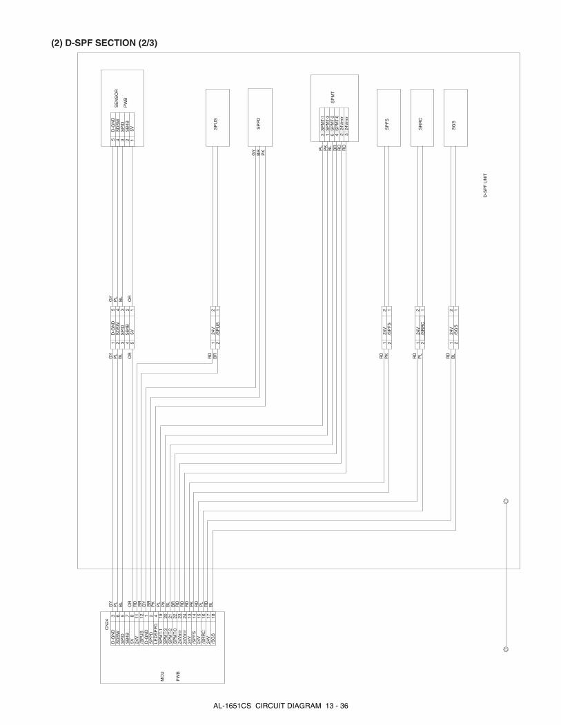
24V
mir
24V
mir
D-G
ND
SD
SW
SP
IDS
B4B
5V /SP
US
SP
MT-
1S
PM
T-3
SP
MT-
2S
PM
T-0
24V
3 6 51 24
LED
SP
PD
SP
PD
/SP
US
5VSB
4BS
PID
SD
SW
D-G
ND
24V
232119212853
D-G
ND
SP
MT-
2
SP
MT-
1
24V
mir
132220411176
24V
SP
MT-
0
SP
MT-
3
1
1
2
233
4
4
5
5 112
2
SP
MT
SP
US
SP
PD
SE
NS
OR
PW
B
5VSB
4BS
PID
SD
SW
D-G
ND
12345G
YG
YG
Y
GY
PL
PL
PL
PL
BL
BL
BL
BL
OR
OR
OR
BR
BR
BR
BR
PK
PK
PK
PK
BR
GY
RD
BR
RD
RD
RD
RD
RD
BL
PL
/SP
FS
24V
112
2S
PF
SR
DP
K
/SR
RC
24V
112
2S
RR
CR
DP
L
/SG
S24
V1
122
SG
SR
DB
L
/SP
FS
1424
V15
/SR
RC
1624
V17
24V
mir
24
/SG
S18
RD
PK
RD
PL
RD
BL
D-S
PF
UN
IT
MC
U
PW
B
CN
24
(2) D-SPF SECTION (2/3)
AL-1651CS CIRCUIT DIAGRAM 13 - 36

10
DIR
3
P3
22
74
NIC
PW
B
81 14
18
1616
17
/PA
CK
1 2392
PB
SY
18
8
P0
P4
D-G
ND
P2
PE
RR
5VP6
11
/ST
B
9
/FLT
5
/IT3
15 2021
21
3 20
/SE
LIN
3
2417
12P
7
23
6
22
MC
U
PW
B
/AF
EE
D3
D-G
ND
CN
16
14
VC
C3
3 6
P1
5
13
/RE
SE
T
SLC
T
19
12 15
245V
4 11
P5
13
10
7 19
2
CN
1
1 2 3 4 5 6 7 8 9 10 11 12 13 14 15 16 17 18 19 20 21 22 23 24 2625
MD
M_I
RQ
PB
_NA
E0
PB
_AD
DR
1
PB
_AD
DR
6
PB
_DAT
A1
PB
_DAT
A5
PB
_DAT
A7
PB
_AD
DR
5
PB
_DAT
A0
PB
_DAT
A4
D-G
ND
PB
_MO
EP
B_N
WE
D-G
ND
PB
_AD
DR
0
PB
_AD
DR
3
D-G
ND
(/FA
X_R
ST
)
PB
_NC
S1
PB
_AD
DR
2
PB
_AD
DR
4
PB
_AD
DR
7D
-GN
D
PB
_DAT
A2
PB
_DAT
A3
PB
_DAT
A6
CN
37
5
D7
D-G
ND
17E
N5V
D-G
ND
16
D1
D4
15 18V
CC
31914
D-G
ND
D3
MS
U_S
T1
2
D0
VC
C3
6 129
/RD
P-G
ND
D2
3
MO
DE
M_I
N
24V
4 2087
CN
38
13
D5
/CS
4
D6
1 1110
TO NE
TW
OR
K
TO T
EL
DIR
3
P3
/PA
CK
PB
SY
P0
P4
D-G
ND
P2
PE
RR
5VP6
/ST
B/F
LT
/IT3
/SE
LIN
3
P7
/AF
EE
D3
D-G
ND
VC
C3
P1
/RE
SE
T
SLC
T
5VP5
MD
M_I
RQ
PB
_NA
E0
PB
_AD
DR
1
PB
_AD
DR
6
PB
_DAT
A1
PB
_DAT
A5
PB
_DAT
A7
PB
_AD
DR
5
PB
_DAT
A0
PB
_DAT
A4
D-G
ND
PB
_MO
EP
B_N
WE
D-G
ND
PB
_AD
DR
0
PB
_AD
DR
3
D-G
ND
(/FA
X_R
ST
)
PB
_NC
S1
PB
_AD
DR
2
PB
_AD
DR
4
PB
_AD
DR
7D
-GN
D
PB
_DAT
A2
PB
_DAT
A3
PB
_DAT
A6
FAX
PW
B
24 182026 25 23 22 21 19 17 67 412 916 5 38101415 13 11 2 1
VO
UT
1V
OU
T2
CN
10
D7
D-G
ND
EN
5V
D-G
ND
D1
D4
VC
C3
D-G
ND
D3
MS
U_S
T1
D0
VC
C3
/RD
P-G
ND
D2
MO
DE
M_I
N
24V
D5
/CS
4
D6
10 8 7 2513 919 18 14 461720 131116 15 12
CN
2
1 2S
PE
AK
ER
CN
1
AL-
1661
CS
(FA
X M
OD
EL)
ON
LY
1 2 3 4
5V U
SB
DAT
A +
DAT
A -
D-G
ND
CN
33
Per
sona
l Com
pute
r(U
SB
PO
RT
)
(3) NIC & FAX SECTION (3/3)
AL-1651CS CIRCUIT DIAGRAM 13 - 37
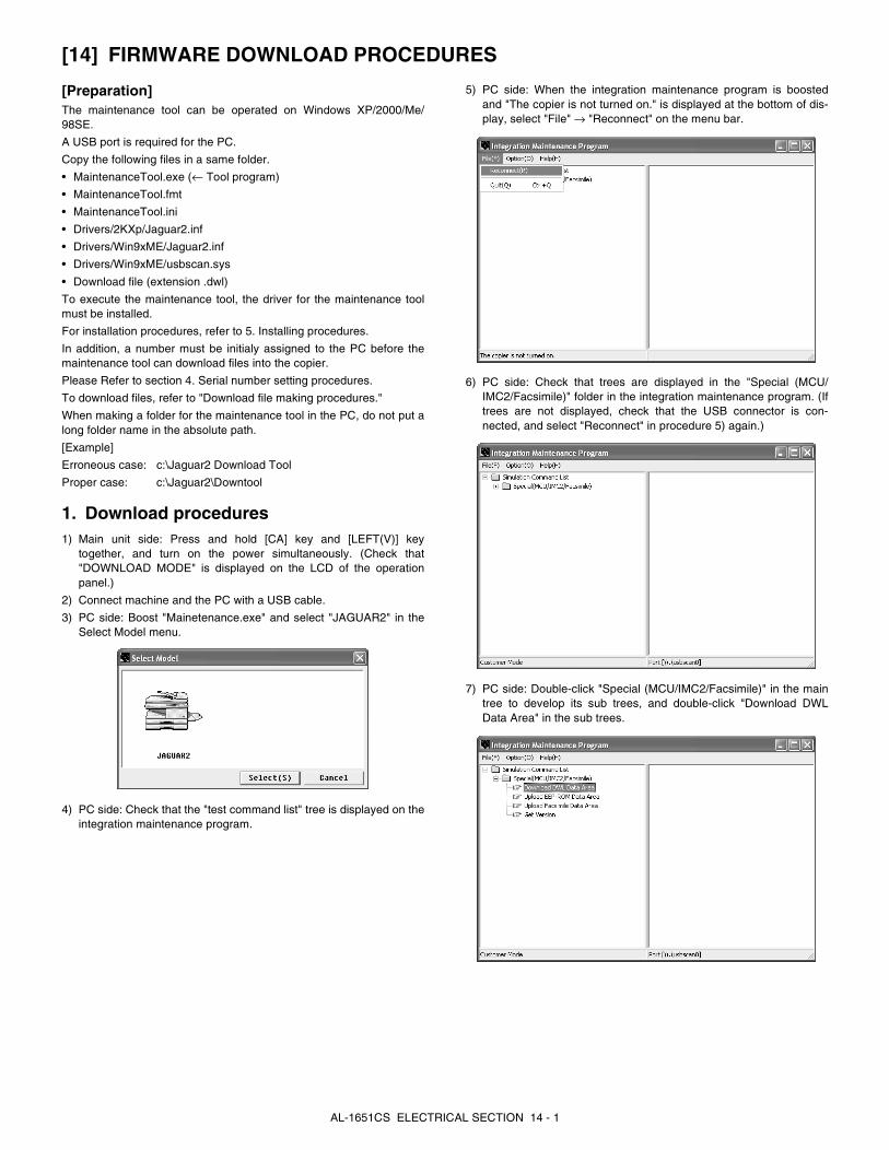
[14] FIRMWARE DOWNLOAD PROCEDURES
[Preparation]The maintenance tool can be operated on Windows XP/2000/Me/98SE.
A USB port is required for the PC.
Copy the following files in a same folder.
• MaintenanceTool.exe (← Tool program)
• MaintenanceTool.fmt
• MaintenanceTool.ini
• Drivers/2KXp/Jaguar2.inf
• Drivers/Win9xME/Jaguar2.inf
• Drivers/Win9xME/usbscan.sys
• Download file (extension .dwl)
To execute the maintenance tool, the driver for the maintenance toolmust be installed.
For installation procedures, refer to 5. Installing procedures.
In addition, a number must be initialy assigned to the PC before themaintenance tool can download files into the copier.
Please Refer to section 4. Serial number setting procedures.
To download files, refer to "Download file making procedures."
When making a folder for the maintenance tool in the PC, do not put along folder name in the absolute path.
[Example]
Erroneous case: c:\Jaguar2 Download Tool
Proper case: c:\Jaguar2\Downtool
1. Download procedures1) Main unit side: Press and hold [CA] key and [LEFT(V)] key
together, and turn on the power simultaneously. (Check that"DOWNLOAD MODE" is displayed on the LCD of the operationpanel.)
2) Connect machine and the PC with a USB cable.
3) PC side: Boost "Mainetenance.exe" and select "JAGUAR2" in theSelect Model menu.
4) PC side: Check that the "test command list" tree is displayed on theintegration maintenance program.
5) PC side: When the integration maintenance program is boostedand "The copier is not turned on." is displayed at the bottom of dis-play, select "File" → "Reconnect" on the menu bar.
6) PC side: Check that trees are displayed in the "Special (MCU/IMC2/Facsimile)" folder in the integration maintenance program. (Iftrees are not displayed, check that the USB connector is con-nected, and select "Reconnect" in procedure 5) again.)
7) PC side: Double-click "Special (MCU/IMC2/Facsimile)" in the maintree to develop its sub trees, and double-click "Download DWLData Area" in the sub trees.
AL-1651CS ELECTRICAL SECTION 14 - 1

8) PC side: Specify the download file (*****.dwl) to be used.
9) PC side: When a download file is specified, downloading is per-formed automatically.
On specifying a download file, "FLASH ERASE" is displayed on theLCD of machine.
10) PC side: When download is completed, the following message isdisplayed.
Completion message: "Download completed."
Note: Since, however, the machine enters the download data writestate, do not turn OFF the power of the machine at this moment.
11) Main unit side: Wait until "DOWNLOAD COMPLETE!" is displayedon the LCD of the operation panel. When "DOWNLOAD COM-PLETE!" is displayed, download is completed.
Turn OFF the power of the machine, and disconnect the USBcable.
12) Terminate the integration maintenance program, and turn ON themachine again.
Download is completed with the above procedures.
Note: When another machine is connected, connect the USB cableagain and select "File" → "Reconnect" on the menu bar of theintegration maintenance program. Repeat the above proceduresfrom 5).
∗∗∗∗ Inhibition during download (Important)If download is failed, the next download may not be executed. Usegreat care not to execute the following items during download.
• Never turn off the machine.
• Never disconnect the download cable (USB cable).
2. Version acquisition procedures1) Main unit side: Press and hold "CA" key and "LEFT(V)" key, and
turn on the power simultaneously. (Check that "DOWNLOADMODE" is displayed on the operation panel of the main unit.)
2) Connect the machine and the PC with a USB cable.
3) PC side: Boost "Mainetenance.exe" and select "JAGUAR2" in the"Select Model" menu.
4) PC side: Check that the "test command list" tree on the integrationmaintenance program.
5) PC side: Boot the integration maintenance program. If "The copieris not turned on." is displayed, select "File" → "Reconnect" on themenu bar.
AL-1651CS ELECTRICAL SECTION 14 - 2
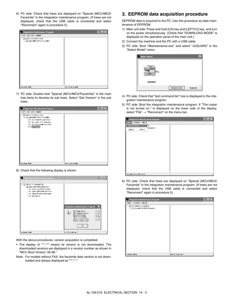
6) PC side: Check that trees are displayed on "Special (MCU/IMC2/Facsimile" in the integration maintenance program. (If trees are notdisplayed, check that the USB cable is connected and select"Reconnect" again in procedure 5).
7) PC side: Double-click "Special (MCU/IMC2/Facsimile)" in the maintree items to develop its sub trees. Select "Get Version" in the subtrees.
8) Check that the following display is shown.
With the above procedures, version acquisition is completed.
• The display of "**.**" means its version is not downloaded. Thedownloaded versions are displayed in a version number as shown in"MCU Boot Version: 00.08."
Note: For models without FAX, the facsimile data version is not down-loaded and always displayed as "**.**."
3. EEPROM data acquisition procedureEEPROM data is acquired to the PC. Use this procedure as data main-tenance of EEPROM.
1) Main unit side: Press and hold [CA] key and [LEFT(V)] key, and turnon the power simultaneously. (Check that "DOWNLOAD MODE" isdisplayed on the operation panel of the main unit.)
2) Connect the machine and the PC with a USB cable.
3) PC side: Boot "Mainetenance.exe" and select "JUGUAR2" in the"Select Model" menu.
4) PC side: Check that "test command list" tree is displayed in the inte-gration maintenance program.
5) PC side: Boot the integration maintenance program. If "The copieris not turned on." is displayed on the lower side of the display,select "File" → "Reconnect" on the menu bar.
6) PC side: Check that trees are displayed on "Special (MCU/IMC2/Facsimile" in the integration maintenance program. (If trees are notdisplayed, check that the USB cable is connected and select"Reconnect" again in procedure 5).
AL-1651CS ELECTRICAL SECTION 14 - 3

7) PC side: Double-click "Special (MCU/IMC2/Facsimile)" to developits sub trees, and select "Upload EEP-ROM Data Area" in the subtrees.
8) PC side: Enter a desired file name, and select "Save."
9) PC side: When upload is completed, the complete message is dis-played.
With the above procedure, the EEPROM data acquisition is completed.
Data acquired by the EEPROM data acquisition procedure are savedin a file with extension of .eep.
4. Serial number settingThe serial number is set to the PC which is used for downloading. Set-ting is required once only, and there is no need to set again whenrebooting the program.
1) PC side: Boot "Mainetenance.exe" and select "JUGARD2" in the"Select Model" menu.
(Only to set the serial number, the PC should not be connected tothe machine.)
2) Select "Option" → "Serial Number Setting" on the menu bar.
3) Enter optional values to "Product Code" and "ID Code" on the menubox.
After completion setting, press [OK] key.
4) The PC number (serial number) has been assigned.
5. Installing procedures<USB integration maintenance program installation>
Driver installation is made on plug-and-play.
<Installation on Windows XP>
1) Main unit side: Press and hold [CA] key and [LEFT(V)] key, and turnon the power simultaneously. (Check that "DOWNLOAD MODE" isdisplayed on the LCD of the operation panel.
2) Connect the machine and the PC with a USB cable.
Product Code (P): Enter number (0 – 99)Enter the product code of “3.”
ID Code(I): Enter number (0 – 99)Assign an individual code to each PC uses“MaintenanceTool.exe.”
AL-1651CS ELECTRICAL SECTION 14 - 4

3) The following display is shown.
Select [Install from a list or specific location] and press <Next> but-ton.
4) Select [Include this location in the search;]. If the search location isnot the folder which includes the maintenance tool driver(Jaguar2.inf), select <Browse>. If the search location is the folderwhich includes the maintenance tool driver, press <Next> button togo to procedure 7).
5) Select the folder which includes the maintenance tool driver(Jaguar2s.inf) and press <OK> button.
(Suppose that the driver is included in C:\Drivers\2kXp folder.)
6) Check the path to the folder which includes the maintenance tooldriver (Jaguar2.inf), and press <Next> button.
7) When the following display is shown, press [Continue Anyway] but-ton.
8) When the following display is shown, installation is completed.
Press <Finish> button.
With the above procedures, installation (on Windows XP) of the inte-gration maintenance program is completed.
AL-1651CS ELECTRICAL SECTION 14 - 5
<Installation on Windows 2000>
1) Main unit side: Press and hold [CA] key and [LEFT(V)] key, and turnon the power simultaneously. (Check that "DOWNLOAD MODE" isdisplayed on the LCD of the operation panel.)
2) Connect the machine and the PC with a USB cable.
3) Check that the Found New Hardware Wizard is displayed, andpress <Next> button.
4) Select [Search for a suitable driver for my device] and press <Next>button.
5) Select [Specify a location] and press <Next> button.
6) Press <Browse> button.
7) Specify the folder which includes the maintenance tool driver(Jaguar2.inf), and press <Open> button.
8) Check that the path to the folder which includes the maintenancetool driver (jaguar2.inf) is displayed, and press <OK> button.
(Suppose that the maintenance tool driver is included in C:\Driv-ers\2kXp folder.)
AL-1651CS ELECTRICAL SECTION 14 - 6
9) Press <Next> button to start installation.
10) When the following display is shown, installation is completed.
Press <Finish> button.
With the above procedures, installation (on Windows 2000) of the inte-gration maintenance program is completed.
<Installation on Windows Me>
1) Main unit side: Press and hold [CA] key and [LEFT(V)] key, and turnon the power simultaneously. (Check that "DOWNLOAD MODE" isdisplayed on the LCD of the operation panel.)
2) Connect the machine and the PC with a USB cable.
3) The following display is shown on the PC side.
Select [Specify the location of the driver], and press <Next> button.
4) Select [Specify a location], specify the folder which includes themaintenance tool driver (Jaguar2.inf) as the search location, andpress <Next> button.
If the search location does not include the maintenance tool driver(Jaguar2.inf), press <Browse> button to specify the folder whichincludes the maintenance tool driver (Jaguar2.inf).
(Suppose that the maintenance tool driver is included inC:\Driver\Win9xME folder.)
5) Press <Next> button to start installation.
6) When the following display is shown, installation is completed.
Press <Finish> button.
With the above procedures, installation (on Windows ME) of the inte-gration maintenance program is completed.
AL-1651CS ELECTRICAL SECTION 14 - 7

LEAD-FREE SOLDER
The PWB’s of this model employs lead-free solder. The “LF” marks indicated on the PWB’s and the Service Manual mean “Lead-Free” solder. The alphabet following the LF mark shows the kind of lead-free solder.
(1) NOTE FOR THE USE OF LEAD-FREE SOLDER THREAD
When repairing a lead-free solder PWB, use lead-free solder thread.Never use conventional lead solder thread, which may cause a breakdown or an accident.Since the melting point of lead-free solder thread is about 40°C higher than that of conventional lead solder thread, the use of the exclusive-usesoldering iron is recommendable.
(2) NOTE FOR SOLDERING WORK
Since the melting point of lead-free solder is about 220°C, which is about 40°C higher than that of conventional lead solder, and its soldering capacity isinferior to conventional one, it is apt to keep the soldering iron in contact with the PWB for longer time. This may cause land separation or may exceedthe heat-resistive temperature of components. Use enough care to separate the soldering iron from the PWB when completion of soldering isconfirmed.Since lead-free solder includes a greater quantity of tin, the iron tip may corrode easily. Turn ON/OFF the soldering iron power frequently.If different-kind solder remains on the soldering iron tip, it is melted together with lead-free solder. To avoid this, clean the soldering iron tip aftercompletion of soldering work.If the soldering iron tip is discolored black during soldering work, clean and file the tip with steel wool or a fine filer.
Example:
5mm
Lead-Free
Solder compositioncode (Refer to thetable at the right.)
<Solder composition code of lead-free solder>
Solder composition
Sn-Ag-Cu
Sn-Ag-BiSn-Ag-Bi-Cu
Sn-Zn-Bi
Sn-In-Ag-Bi
Sn-Cu-Ni
Sn-Ag-Sb
Bi-Sn-Ag-PBi-Sn-Ag
a
b
z
i
n
s
p
Solder composition code
a
(Danish) ADVARSEL !Lithiumbatteri – Eksplosionsfare ved fejlagtig håndtering.
Udskiftning må kun ske med batteriaf samme fabrikat og type.
Levér det brugte batteri tilbage til leverandoren.
(English) Caution !Danger of explosion if battery is incorrectly replaced.
Replace only with the same or equivalent typerecommended by the manufacturer.
Dispose of used batteries according to manufacturer’s instructions.
(Finnish) VAROITUSParisto voi räjähtää, jos se on virheellisesti asennettu.
Vaihda paristo ainoastaan laitevalmistajan suosittelemaantyyppiin. Hävitä käytetty paristo valmistajan ohjeiden
mukaisesti.
(French) ATTENTIONIl y a danger d’explosion s’ il y a remplacement incorrect
de la batterie. Remplacer uniquement avec une batterie dumême type ou d’un type équivalent recommandé par
le constructeur.Mettre au rebut les batteries usagées conformément aux
instructions du fabricant.
(Swedish) VARNINGExplosionsfara vid felaktigt batteribyte.
Använd samma batterityp eller en ekvivalenttyp som rekommenderas av apparattillverkaren.
Kassera använt batteri enligt fabrikantensinstruktion.
(German) AchtungExplosionsgefahr bei Verwendung inkorrekter Batterien.
Als Ersatzbatterien dürfen nur Batterien vom gleichen Typ odervom Hersteller empfohlene Batterien verwendet werden.Entsorgung der gebrauchten Batterien nur nach den vom
Hersteller angegebenen Anweisungen.
CAUTION FOR BATTERY REPLACEMENT
CAUTION FOR BATTERY DISPOSAL
(For USA, CANADA)
"BATTERY DISPOSAL"THIS PRODUCT CONTAINS A LITHIUM PRIMARY
(MANGANESS DIOXIDE) MEMORY BACK-UP BATTERY THAT MUST BE DISPOSED OF PROPERLY. REMOVE THE
BATTERY FROM THE PRODUCT AND CONTACT YOUR LOCAL ENVIRONMENTAL AGENCIES FOR INFORMATION
ON RECYCLING AND DISPOSAL OPTIONS.
"TRAITEMENT DES PILES USAGÉES"CE PRODUIT CONTIENT UNE PILE DE SAUVEGARDE DE
MÉMOIRE LITHIUM PRIMAIRE (DIOXYDE DE MANGANÈSE) QUI DOIT ÊTRE TRAITÉE CORRECTEMENT. ENLEVEZ LA PILE DU PRODUIT ET PRENEZ CONTACT AVEC VOTRE
AGENCE ENVIRONNEMENTALE LOCALE POUR DES INFORMATIONS SUR LES MÉTHODES DE RECYCLAGE ET
DE TRAITEMENT.

All rights reserved.Printed in Japan.
No part of this publication may be reproduced,stored in a retrieval system, or transmitted,
in any form or by any means,electronic; mechanical; photocopying; recording or otherwise
without prior written permission of the publisher.
Trademark acknowledgements• Microsoft® Windows® operating system is a trademark or copyright of Microsoft
Corporation in the U.S.A. and other countries.
• Windows® 95, Windows® 98, Windows® Me, Windows NT® 4.0, Windows® 2000, and Windows® XP are trademarks or copyrights of Microsoft Corporation in the U.S.A. and other countries.
• IBM and PC/AT are trademarks of International Business Machines Corporation.
• Acrobat® Reader Copyright® 1987- 2002 Adobe Systems Incorporated. All rights reserved. Adobe, the Adobe logo, Acrobat, and the Acrobat logo are trademarks of Adobe Systems Incorporated.
• All other trademarks and copyrights are the property of their respective owners.
SHARP CORPORATIONDigital Document System GroupProducts Quality Assurance DepartmentYamatokoriyama, Nara 639-1186, Japan
2003 September Printed in Japan
Top Related