


Languages
Pages
Legal


Acer Service Manual
Service Manual LCD Monitor Acer
AL2017
0

1
1
Service Manual Versions and Revision
No. Version Release Date Revision
1 1.0 2007/01/18 Initial Release
Copyright Copyright 2007 InnoLux Tech. Corp. Ltd All Rights Reserved This manual may not, in whole or in part, be copied, Photocopied, reproduced, translated, or converted to any electronic or machine readable form without prior written permission of InnoLux Tech. Corp. Ltd. Acer AL2017 Service Manual
Acer Service Manual
2
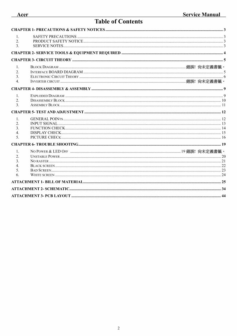
Table of Contents CHAPTER 1- PRECAUTIONS & SAFETY NOTICES ..................................................................................................................... 3
1. SAFETY PRECAUTIONS ................................................................................................................................................. 3 2. PRODUCT SAFETY NOTICE........................................................................................................................................... 3 3. SERVICE NOTES............................................................................................................................................................... 3
CHAPTER 2- SERVICE TOOLS & EQUIPMENT REQUIRED ..................................................................................................... 4 CHAPTER 3- CIRCUIT THEORY ...................................................................................................................................................... 5
1. BLOCK DIAGRAM ..............................................................................................................................錯誤! 尚未定義書籤。 2. INTERFACE BOARD DIAGRAM ........................................................................................................................................... 5 3. ELECTRONIC CIRCUIT THEORY ............................................................................................................................................... 6 4. INVERTER CIRCUIT .............................................................................................................................錯誤! 尚未定義書籤。
CHAPTER 4- DISASSEMBLY & ASSEMBLY ................................................................................................................................... 9 1. EXPLODED DIAGRAM ............................................................................................................................................................. 9 2. DISASSEMBLY BLOCK........................................................................................................................................................... 10 3. ASSEMBLY BLOCK ................................................................................................................................................................ 11
CHAPTER 5- TEST AND ADJUSTMENT ........................................................................................................................................ 12 1. GENERAL POINTS............................................................................................................................................................. 12 2. INPUT SIGNAL .................................................................................................................................................................. 13 3. FUNCTION CHECK........................................................................................................................................................... 14 4. DISPLAY CHECK............................................................................................................................................................... 15 5. PICTURE CHECK............................................................................................................................................................... 16
CHAPTER 6- TROUBLE SHOOTING.............................................................................................................................................. 19 1. NO POWER & LED OFF .............................................................................................................. 19 錯誤! 尚未定義書籤。 2. UNSTABLE POWER ................................................................................................................................................................ 20 3. NO RASTER ........................................................................................................................................................................... 21 4. BLACK SCREEN..................................................................................................................................................................... 22 5. BAD SCREEN......................................................................................................................................................................... 23 6. WHITE SCREEN ..................................................................................................................................................................... 24
ATTACHMENT 1- BILL OF MATERIAL......................................................................................................................................... 25 ATTACHMENT 2- SCHEMATIC....................................................................................................................................................... 34 ATTACHMENT 3- PCB LAYOUT ..................................................................................................................................................... 44

Acer Service Manual
3
Chapter 1- PRECAUTIONS & SAFETY NOTICES
1. SAFETY PRECAUTIONS This monitor is manufactured and tested on a ground principle that a user’s safety comes first. However, improper used or installation may cause damage to the monitor as well as to the user.
WARNINGS: This monitor should be operated only at the correct power sources indicated on the label on the rear
of the monitor. If you’re unsure of the power supply in you residence, consult your local dealer or Power Company.
Do not try to repair the monitor by yourself, as it contains no user-serviceable parts. This monitor should only be repaired by a qualified technician.
Do not remove the monitor cabinet. There are high-voltage parts inside that may cause electric shock to human bodies.
Stop using the monitor if the cabinet is damaged. Have it checked by a service technician. Put your monitor only in a lean, cool, dry environment. If it gets wet, unplug the power cable
immediately and consult your closed dealer. Always unplug the monitor before cleaning it. Clean the cabinet with a clean, dry cloth. Apply
non-ammonia based cleaner onto the cloth, not directly onto the class screen. Do not place heavy objects on the monitor or power cord.
2. PRODUCT SAFETY NOTICE Many electrical and mechanical parts in this chassis have special safety visual inspections and the protection afforded by them cannot necessarily be obtained by using replacement components rated for higher voltage, wattage, etc. Before replacing any of these components read the parts list in this manual carefully. The use of substitute replacement parts, which do not have the same safety characteristics as specified in the parts list, may create shock, fire, or other hazards.
3. SERVICE NOTES When replacing parts or circuit boards, clamp the lead wires around terminals before soldering.
Keep wires away from high voltage, high temperature components and sharp edges.
Keep wires in their original position so as to reduce interference.
Adjustment of this product please refers to the user’ manual.
Acer Service Manual
4
Chapter 2- SERVICE TOOLS & EQUIPMENT REQUIRED
1. SIGNAL GENERATOR 2. MULTIMETER 3. SCREW DRIVER 4. OSCILLOSCOPE 5. Soldering IRON 6. SOLDER 7. VGA Cable (15pins point to point) 8. Color Analyzer 9. Myson412 ISP Board 10. EDID Board 11. EDID program file

Acer Service Manual
Chapter 3- CIRCUIT THEORY
1. Monitor Block Diagram The LCD Monitor contains an interface board, and inverter/power/Audio board, keypad board and flat panel. In Inverter/power/Audio board, power section supplies +14V & +5V for Inverter/Audio and Interface board used. The inverter section drives the backlight of panel and the DC-DC conversion.
2. Interface BOARD DIAGRAM
A/D&Scaler&MCU
Red
Green
Hsync
Vsync
Blue
VGADVI
(Option)
SDA
SCL
VGADDC
OSD(EEprom)
Key-pad
FlashDVIDDC
To LCDmodule
3. Electronic Circuit Theory 1.1 Switching Mode Power Supply
1.1.1 AC Current Input Circuit
P801 is a connector for connecting AC Power. F801 is a fuse to protect all the circuit. AC input voltage is from 90v to 264V. R801 and R802 joined between two inputting main circuit to prevent man from shock. L801 is used to clear up low frequency wave. C801 and C802 are used to discharge the waves that L801 produced. High frequency waves are damped by C801 and C802. D801 is a rectifier which composed of 4 build-in diodes, it inverts AC to DC.
1.1.2 High Voltage to Low Voltage Control Circuit C804 is used to smooth the wave from rectifier. IC802 is a highly integrated PWM controller.
When rectified DC high voltage is applied to the HV pin during start-up, the MOSFET Q804 is 5
Acer Service Manual
6
initially off, and the Vcc pin capacitor is charged. When the Vcc pin voltage reaches approximately 14V, the control circuitry is activated and the soft-start begins. The soft-start circuit gradually increases the duty cycle of the MOSFET from zero to the maximum value over approximately 4ms. If no external feedback/supply current is fed into the FB pin by the end of the soft-start, the current Setpoint will be above the fault level, FAULT flag is raised, if the FAULT duration exceeds 80ms, the output controller disable resistor R808, R809, R810, R811 are for line over voltage shutdown(OVP)
When PWM is turned off, the main current flow will be consumed through R804 and D802, This will prevent MOSFET Q804 from being damaged under large current impulse and voltage spike.
D803 and C807 to provide internal Auxiliary voltage to Vcc pin during normal operation. Otherwise, error amplifier and feedback current input the FB pin for duty cycle control.
1.1.3 DC_5V and DC_16V Output Circuit For DC 5V, D805 is used to rectify the inducted current. R828 and C814 are used to store
energy when current is reversed. The parts including C818, C822, C820,L803 are used to smooth the current waves.
For DC 16V, D803 is used to rectify the inducted current. R827 and C813 are used to store energy when current is reversed. The parts including C815, C817 and L802 are used to smooth the current waves.
1.1.4 Feedback and OVP Protect Circuit Pin R of IC803 is supplied 2.5-v stable voltage. It connects to 5V and 16V output through
R822, R823 and R824. R822, R823 and R824 are output sampling resistor. When the sampling voltage more than 2.5V or less than 2.5V, current of FB IC802 will change, this can change the voltage from T801.
OVP Protect Circuit: When output is overvoltage, the auxiliary winding voltage will be increased, when it reaches about 14V. Q803 is triggered . It makes the IC802 Pin 1 exceed 5V, then the IC802 output will be disabled.
Q801, R816, R817 and ZD803 make up of dummy loading circuit. For start-up sequence, during 5V output take place high loading first, this dummy loading circuit operated to insure 16V not be increased.
1.2 Interface Board Circuit 1.2.1 RGB CAPTURE
- Signal RED,GREEN,BLUE input through CN103 #1,#2,#3, via R105,FB101, R101,R106, FB102 ,R102, R107,FB103,R103, Stop DC via C101, C102 and C103, and then enter into U104 (TSUM56AWHK) analog input terminal #59,#56,#54, and then TSUM56AWHK deals with signal internally. D101, D102, D103 are ESD protector to prevent U104 from ESD.
- Signal DDC_SCL (series clock) inputs via CN103#15, and then passes through ZD104 Zener for ESD protection, via R121, goes into EDID EEPROM IC U102 #6.
- Signal DDC_SDA (series data) inputs via CN102 #12, and then passes through ZD105 Zener for ESD protection, via R122, goes into EDID EEPROM IC U102 #5.
- Signal TTL vertical sync. (Vsync) inputs via CN103 #14, and then clamped by D103 Zener, passes through R116, and then goes into IC U104 #64.
- Signal TTL horizontal sync. (Hsync) inputs via CN103 #13, and then clamped by D102 Zener, passes through FB104,R115, and then goes into IC U104 #63.
- CN103#5 is defined as cable detect pin, this detector realize passes through R113 ,go into U104#26, and ZD109 is ESD protector.
- U102 +5V is supplied by PC via CN103#9 with ZD101 for ESD protection, or supplied by Monitor self via D104.
- U102 is an EEPROM IC which is memory and EDID data saved in it.

Acer Service Manual
7
1.2.2 DVI CAPTURE - Differential Signal input RX0+,RX0-,RX1+,RX1-,RX2+,RX2-,RXC+,RXC- through CN102
#18,#17,#10,#9,#2,#1,#23,#24 via R130, R131, R132, R133, R134, R135, R137, R138 enter into U104 Digital input terminal #45,#46,#42,#43,#39,#40,#48,#49, and then TSUM56AWHK deals with signal internally.
- Signal DDC_SCL (series clock) inputs via CN102#6, and then passes through ZD106 Zener for ESD protection, via R126, goes into EDID EEPROM IC U101 #6.
- Signal DDC_SDA (series data) inputs via CN102 #7, and then passes through ZD107 Zener for ESD protection, via R127, goes into EDID EEPROM IC U101 #5.
- CN102 #16 is defined as cable detect pin, this detector realize passes through R125 ,go into U104#27, and D106 is ESD protector.
- U101 +5V is supplied by PC via CN102#14 with ZD108 for ESD protection, or supplied by Monitor self via D107.
- U102 is an EEPROM IC which is memory and EDID data saved in it.
1.2.3 Buttons Control - Button “Power” on front of bezel connects to scaler TSUMU58WHJ pin #4 through R159, via
CN102#8.
- Button “MENU” on front of bezel connects to scaler TSUMU58WHJ pin #119 through R153,via CN102#1; Button “>” (Rihgt) on front bezel connects to scaler TSUMU58WHJ pin #120 through R154,via CN102#2; Button “<” (Left) on front bezel connects to scaler TSUMU58WHJ pin #121 through R155,via CN102#3;Button “AUTO” on front bezel connects to scaler TSUMU58WHJ pin #122 through R156,via CN102#4;
- U107 is an EEPROM IC which memory OSD setting and save the value adjusted by user.
- LED Indicator
When monitor normally working, scaler TSUMU58WHJ pin #124 sends out a low potential, via R107, switch on Q105, then flows to CN102 #7, LED Green ON.
When in “Suspend” mode, scaler TSUMU58WHJ pin #123 sends out a low potential, via R102, switch on Q102, then flows to CN102 #5, LED Amber ON.
1.2.4 Scaling IC (U104 tsum56AWHK)
- U104 #105~#114 output 8 bit even LVDS digital data to panel control circuit through CN106. - U104 #118~#127 output 8 bit odd LVDS digital data to panel control circuit through CN106. - U104 #75 output ”H” potential to make Q106 conducted, and then make Q103 conducted, +5V flow
to CN106#1~#3 as Panel Vdd . - U104 #20 output,”L” ”H” potential to control Inverter on/off. - U104 #21 outputs Brightness “PWM” signals to control CCFL brightness. - TCLK by Crystal 14.318MHz input to U104 #32.
Please refer to tsum56AWHK Pin Assignments table in page
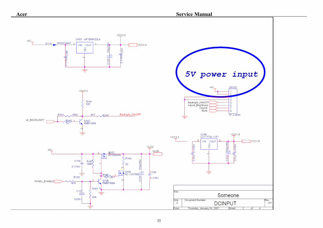
1.2.5 Regulator Circuit - +5V is from powerboard CN103 #1 and CN102 - +3.3V generates from +5V through D116 and C168 filtering and U103 which is output +3.3V LDO - +1.8V generates from +3.3V through C143 filtering and U108 which is output +1.8V LDO, for U104
used.
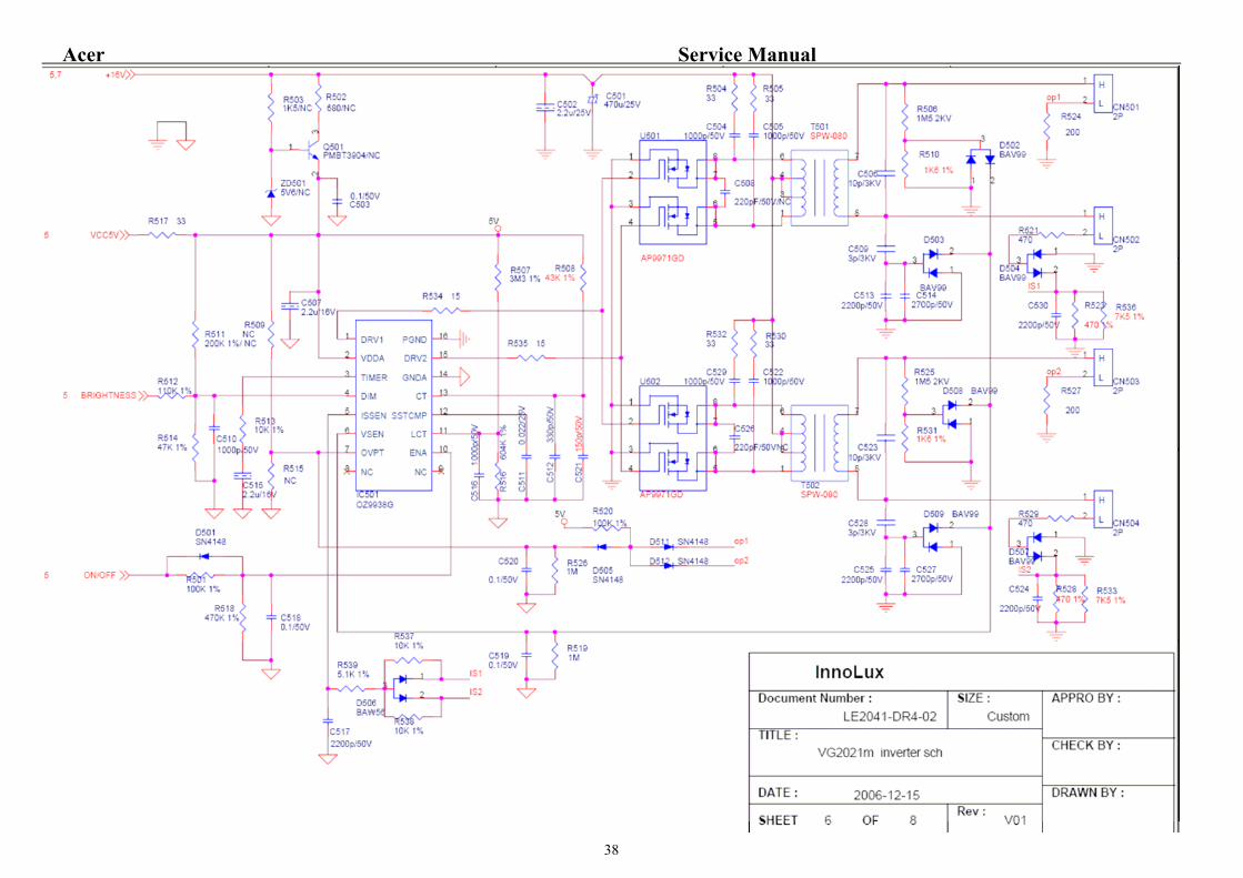
1.3 Inverter circuit Power supply 5V then pass through R517 to IC501. The extra PWM pulse signal
(BRIGHTNESS signal) input to control IC through R512, R514, C510, The LCT pin is set to a DC voltage of 0.7V by using a resistor divider(R507, R516), change the duty of PWM pulse, will regulate the lamp current. The ON/OFF voltage connect to pin10 of IC501 through D501, R501,
Acer Service Manual
8
A voltage of 2V to pin10 of IC501 enables the IC and activates the striking timer. The SSTCMP pin of IC501 performs the soft function, the C511 set the time of SST. The operation frequency determined by external capacitor C512, C521 and resistor R508 connected at CT pin of IC501. C515 connect the TIMER pin of IC501, the capacitor to set striking time and shunt down delay time. DRV!, DRV2 output for power MOSFET U501, U502.
OZ9938 provides two drive signals for U501, U502, and they work in push pull topology driving, two transformers are connected in parallel with each transformer driving two lamps in series. Turning each N-Channel MOSFET “on/off” complementarily, produces an alternating current through the transformer primary and secondary. The “on” duration of the switches determines the amount of energy delivered to the CCFLs. R504, C504, R505, C505, R532, C529, R530, C522 are snubber networks, they suppress Voltage transient spike in drain of power MOSFET.
R506, R510, C509, C513, C514, R525, R531, C528, C525, and C527 are connected between high voltage output connector and ground, the divided AC voltage is inverted DC voltage through D502, D503, D508, and D509. The sense voltage feed back to VSEN (pin 6 of IC501) for an over voltage/over current condition during normal operation. R528, R533,R523,R536 are current sense resistor, current sense signal feed back to Isense (pin 5 of IC501) for lamp “ON” detection.

Acer Service Manual
Chapter 4- Disassembly & Assembly
1. Exploded Diagram Exploded drawing(With DVI)
9

Acer Service Manual
10
Exploded drawing(W/O DVI) (We will update later)

Acer Service Manual 2. Disassembly Block
4. LE2018 BOM Structure
11
PCBA INV.&DC-DC *1 M3*5,Zn ROHS *4 M3*6,W/W-SPR Zn ROHS *1 PCBA I/F BOARD *1
CABLE 30 PIN FFC BOLT,#4-40x11.8,Ni ROHS *4 TAPE ACE *3 M3*5,Zn ROHS *1
PANEL CMO M201P1-L01
ASSY PANEL*1
CHASSIS *1 Gasket,W8*H3*L50*1 Foil,AL,L60*W35*1 KEY PAD*1
CABLE *1 T3*6,Zn ROHS *1
BACK COVER*1
ASSY BEZEL*1
BEZEL*1 BUTTON,POWER KEY*1 BUTTON,FUNCTION*1 LENS*1
ASSY STAND*1 SCREW,P,CROSS,M4*8,BLACK,NL(NYLOK) SCREW,B,CROSS,T.T-4*8,BLK ROHS*2
LE 2018 LCD Monitor
STAND*1 HINGE*1 BRACKET FINGER*1 SCREW,B,CROSS,W/W-SPR,M4*20,Zn ROHS *3
ASSY BASE*1
BASE*1 RUBBER*4 GASKET*1 PLATE,BASE*1 T4*6,Zn, ROHS *2
HINGE COVER*1
SPEAKER*1

Acer Service Manual
5. LE2018 DIS-assembly Block
12
Note: The DIS assembly direction please following direction of arrowhead
ASSY PANEL UNIT CHASSIS *1 PCBA I/F BOARD *1 PCBA INV.&DC-DC *1 CABLE KEYPAD*1 CABLE 30P FFC BOLT,#4-40x11.8,Ni ROHS *4 M3*5,Ni ROHS *5 TAPE ACE *3 M3*6,W/W-SPR Zn ROHS*1 Gasket,W8*H3*L50*1 Foil,AL,L60*W35*1
ASSY, BASE BASE*1 RUBBER FOOT *4 GASKET*1 PLATE,BASE*1 T4*6,Zn, ROHS *2
BACK COVER
ASSY STAND M4*8,Black Zn,NL ROHS *4 SCREW,B,CROSS,T.T-4*8,BLK ROHS*2
BRACKET FINGER *1 HINGE *1 STAND SCREW,B,CROSS,W/W-SPR,M4*20,Zn ROHS *3
ASSY FRONT BEZEL
LE 2018 LCD Monitor
FRONT BEZEL *1 FUNCTION KEY *1 POWER BUTTON *1 LED LENS
HINGE COVER*1
SPEAKER*1
PANEL CMO M201P1-L01

Acer Service Manual Process To Access Factory Mode
Power Off
Press “AUTO"& "MENU"button at the same time
Power On
Release the “AUTO"& "MENU"button
Press “MENU" Button
Press “<" Button
Press “Menu" Button
Enter the factory Mode
13
Acer Service Manual
14
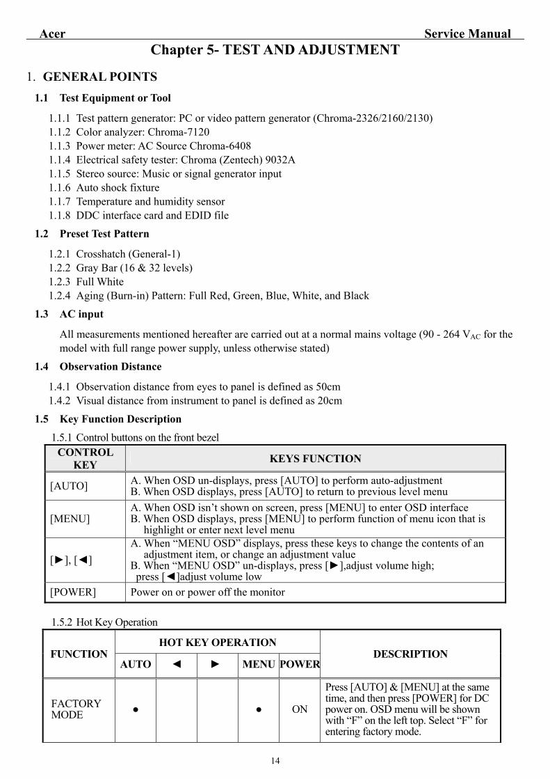
Chapter 5- TEST AND ADJUSTMENT
1. GENERAL POINTS 1.1 Test Equipment or Tool
1.1.1 Test pattern generator: PC or video pattern generator (Chroma-2326/2160/2130) 1.1.2 Color analyzer: Chroma-7120 1.1.3 Power meter: AC Source Chroma-6408 1.1.4 Electrical safety tester: Chroma (Zentech) 9032A 1.1.5 Stereo source: Music or signal generator input 1.1.6 Auto shock fixture 1.1.7 Temperature and humidity sensor 1.1.8 DDC interface card and EDID file
1.2 Preset Test Pattern
1.2.1 Crosshatch (General-1) 1.2.2 Gray Bar (16 & 32 levels) 1.2.3 Full White 1.2.4 Aging (Burn-in) Pattern: Full Red, Green, Blue, White, and Black
1.3 AC input
All measurements mentioned hereafter are carried out at a normal mains voltage (90 - 264 VAC for the model with full range power supply, unless otherwise stated)
1.4 Observation Distance
1.4.1 Observation distance from eyes to panel is defined as 50cm 1.4.2 Visual distance from instrument to panel is defined as 20cm
1.5 Key Function Description
1.5.1 Control buttons on the front bezel CONTROL
KEY KEYS FUNCTION
[AUTO] A. When OSD un-displays, press [AUTO] to perform auto-adjustment B. When OSD displays, press [AUTO] to return to previous level menu
[MENU] A. When OSD isn’t shown on screen, press [MENU] to enter OSD interface B. When OSD displays, press [MENU] to perform function of menu icon that is
highlight or enter next level menu
[], [] A. When “MENU OSD” displays, press these keys to change the contents of an
adjustment item, or change an adjustment value B. When “MENU OSD” un-displays, press [],adjust volume high; press []adjust volume low
[POWER] Power on or power off the monitor
1.5.2 Hot Key Operation
HOT KEY OPERATION FUNCTION
AUTO MENU POWERDESCRIPTION
FACTORY MODE ON
Press [AUTO] & [MENU] at the same time, and then press [POWER] for DC power on. OSD menu will be shown with “F” on the left top. Select “F” for entering factory mode.
Acer Service Manual
15
1.6 Burn-in (Aging) Pattern
1.6.1 Burn-in patterns are: full Red, Green, Blue, White and Blac 1.6.2 Stop burn-in pattern by providing with video signal from D-sub connector 1.6.3 Enter or exit burn-in mode by setting “burn-in” to be “on” or “off” in the factory mode
1.7 Warm Up
All test units have to be done warm up after at least 2 hours in a room with temperature of 40±5°C. (Except particular requirement)
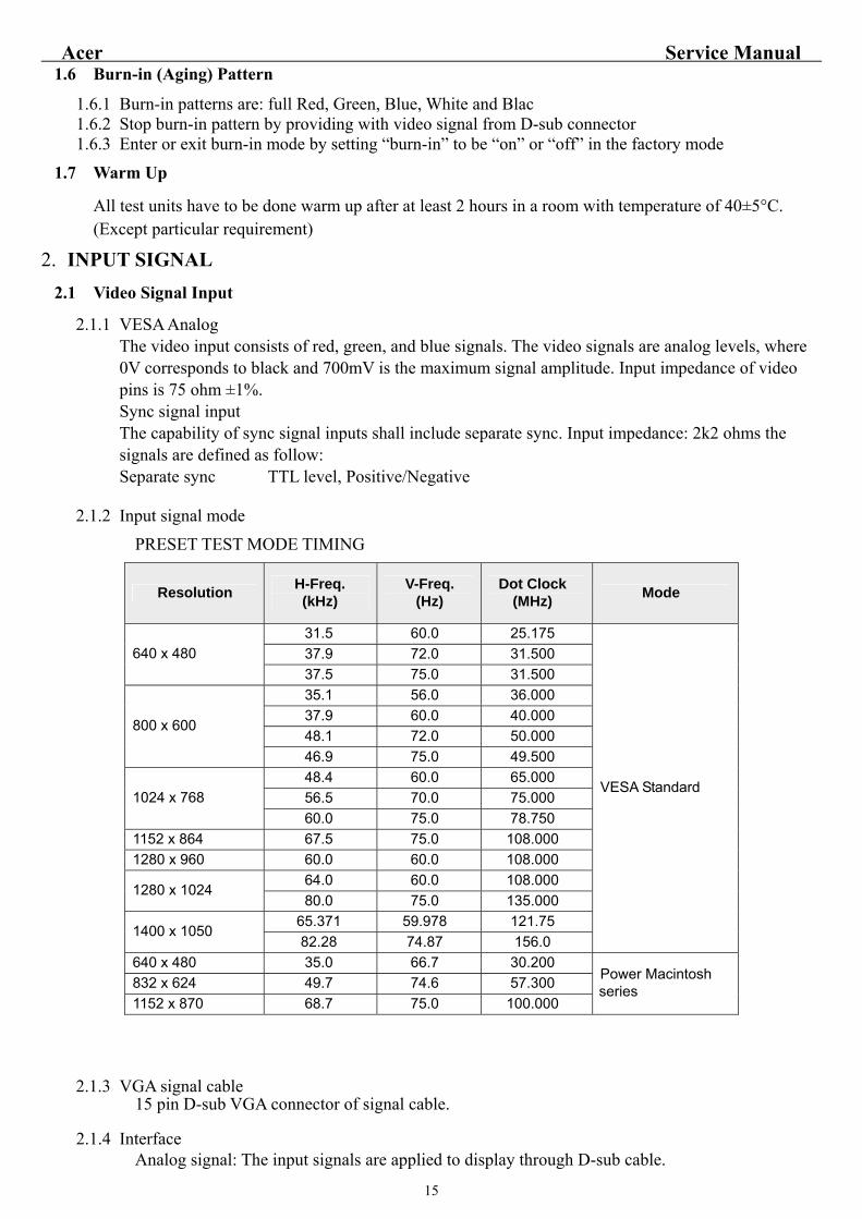
2. INPUT SIGNAL 2.1 Video Signal Input
2.1.1 VESA Analog The video input consists of red, green, and blue signals. The video signals are analog levels, where 0V corresponds to black and 700mV is the maximum signal amplitude. Input impedance of video pins is 75 ohm ±1%. Sync signal input The capability of sync signal inputs shall include separate sync. Input impedance: 2k2 ohms the signals are defined as follow: Separate sync TTL level, Positive/Negative
2.1.2 Input signal mode
PRESET TEST MODE TIMING
Resolution H-Freq. (kHz)
V-Freq. (Hz)
Dot Clock (MHz) Mode
31.5 60.0 25.175 37.9 72.0 31.500 640 x 480 37.5 75.0 31.500 35.1 56.0 36.000 37.9 60.0 40.000 48.1 72.0 50.000
800 x 600
46.9 75.0 49.500 48.4 60.0 65.000 56.5 70.0 75.000 1024 x 768 60.0 75.0 78.750
1152 x 864 67.5 75.0 108.000 1280 x 960 60.0 60.0 108.000
64.0 60.0 108.000 1280 x 1024
80.0 75.0 135.000 65.371 59.978 121.75
1400 x 1050 82.28 74.87 156.0
VESA Standard
640 x 480 35.0 66.7 30.200 832 x 624 49.7 74.6 57.300 1152 x 870 68.7 75.0 100.000
Power Macintosh series
2.1.3 VGA signal cable
15 pin D-sub VGA connector of signal cable.
2.1.4 Interface Analog signal: The input signals are applied to display through D-sub cable.
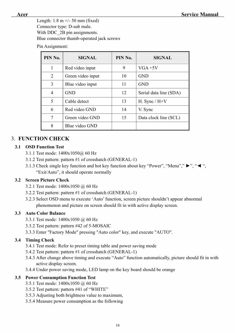
Acer Service Manual Length: 1.8 m +/- 50 mm (fixed) Connector type: D-sub male. With DDC_2B pin assignments. Blue connector thumb-operated jack screws
Pin Assignment:
16
PIN No. SIGNAL PIN No. SIGNAL
1 Red video input 9 VGA +5V
GND 2 Green video input 10
3 Blue video input 11 GND
4 GND 12 Serial data line (SDA)
5 Cable detect 13 H. Sync / H+V
6 Red video GND 14 V. Sync
7 Green video GND 15 Data clock line (SCL)
8 Blue video GND
3. FUNCTION CHECK 3.1 OSD Function Test
3.1.1 Test mode: 1400x1050@ 60 Hz 3.1.2 Test pattern: pattern #1 of crosshatch (GENERAL-1) 3.1.3 Check single key function and hot key function about key “Power”, “Menu”,” ”, “ “,
“Exit/Auto”, it should operate normally
3.2 Screen Picture Check 3.2.1 Test mode: 1400x1050 @ 60 Hz 3.2.2 Test pattern: pattern #1 of crosshatch (GENERAL-1) 3.2.3 Select OSD menu to execute ‘Auto’ function, screen picture shouldn’t appear abnormal
phenomenon and picture on screen should fit in with active display screen.
3.3 Auto Color Balance 3.3.1 Test mode: 1400x1050 @ 60 Hz 3.3.2 Test pattern: pattern #42 of 5-MOSAIC 3.3.3 Enter "Factory Mode" pressing "Auto color" key, and execute "AUTO".
3.4 Timing Check 3.4.1 Test mode: Refer to preset timing table and power saving mode 3.4.2 Test pattern: pattern #1 of crosshatch (GENERAL-1) 3.4.3 After change above timing and execute “Auto” function automatically, picture should fit in with
active display screen. 3.4.4 Under power saving mode, LED lamp on the key board should be orange
3.5 Power Consumption Function Test 3.5.1 Test mode: 1400x1050 @ 60 Hz 3.5.2 Test pattern: pattern #41 of “WHITE” 3.5.3 Adjusting both brightness value to maximum, 3.5.4 Measure power consumption as the following
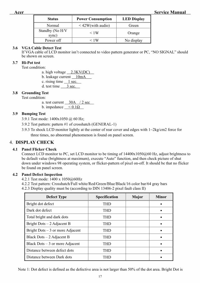
Acer Service Manual
17
Status Power Consumption LED Display Normal < 42W(with audio) Green
Standby (No H/V sync) < 1W Orange
Power off < 1W No display
3.6 VGA Cable Detect Test If VGA cable of LCD monitor isn’t connected to video pattern generator or PC, “NO SIGNAL” should be shown on screen.
3.7 Hi-Pot test Test condition:
a. high voltage 2.3KV(DC) b. leakage current 10mA c. rising time 1 sec. d. test time 3 sec.
3.8 Grounding Test Test condition:
a. test current 30A / 2 sec b. impedance < 0.1Ω
3.9 Bumping Test 3.9.1 Test mode: 1400x1050 @ 60 Hz; 3.9.2 Test pattern: pattern #1 of crosshatch (GENERAL-1) 3.9.3 To shock LCD monitor lightly at the center of rear cover and edges with 1~2kg/cm2 force for
three times, no abnormal phenomenon is found on panel screen.
4. DISPLAY CHECK 4.1 Panel Flicker Check
Connect LCD monitor to PC, set LCD monitor to be timing of 14400x1050@60 Hz, adjust brightness to be default value (brightness at maximum), execute “Auto” function, and then check picture of shut down under windows 98 operating system, or flicker-pattern of pixel on-off. It should be that no flicker be found on panel screen.
4.2 Panel Defect Inspection 4.2.1 Test mode: 1400 x 1050@60Hz 4.2.2 Test pattern: Crosshatch/Full white/Red/Green/Blue/Black/16 color bar/64 gray bars 4.2.3 Display quality must be (according to DIN 13406-2 pixel fault class II)
Defect Type Specification Major Minor
Bright dot defect THD ․ Dark dot defect THD ․ Total bright and dark dots THD ․ Bright Dots – 2 Adjacent B THD ․ Bright Dots – 3 or more Adjacent THD ․ Black Dots – 2 Adjacent B THD ․ Black Dots – 3 or more Adjacent THD ․ Distance between defect dots THD ․ Distance between Dark dots THD ․
Note 1: Dot defect is defined as the defective area is not larger than 50% of the dot area. Bright Dot is
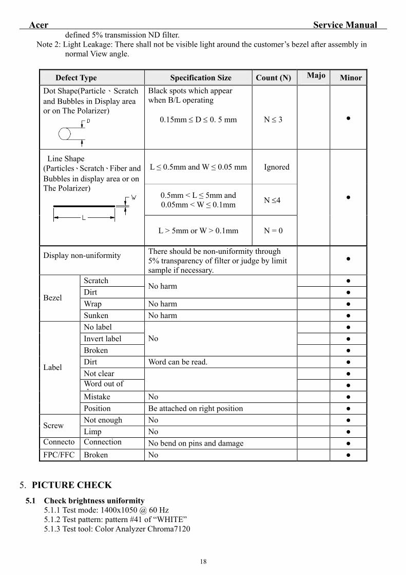
Acer Service Manual defined 5% transmission ND filter.
Note 2: Light Leakage: There shall not be visible light around the customer’s bezel after assembly in normal View angle.
18
5. PICTURE CHECK 5.1 Check brightness uniformity
5.1.1 Test mode: 1400x1050 @ 60 Hz 5.1.2 Test pattern: pattern #41 of “WHITE” 5.1.3 Test tool: Color Analyzer Chroma7120
Defect Type Specification Size Count (N) Major
Minor Black spots which appear
when B/L operating Dot Shape(Particle、Scratch
and Bubbles in Display area or on The Polarizer)
0.15mm ≤ D ≤ 0. 5 mm N ≤ 3
L ≤ 0.5mm and W ≤ 0.05 mm Ignored
0.5mm < L ≤ 5mm and 0.05mm < W ≤ 0.1mm N ≤4
Line Shape (Particles、Scratch、Fiber and Bubbles in display area or on The Polarizer)
L > 5mm or W > 0.1mm N = 0
There should be non-uniformity through 5% transparency of filter or judge by limit sample if necessary.
Display non-uniformity
Scratch No harm
Dirt Wrap No harm
Bezel
Sunken No harm No label Invert label No Broken Dirt Word can be read. Not clear
Label Word out of
hMistake No Position Be attached on right position Not enough No
Screw Limp No
Connecto Connection No bend on pins and damage t tFPC/FFC Broken No
Acer Service Manual
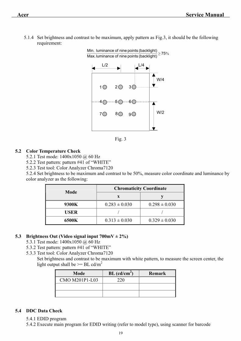
5.1.4 Set brightness and contrast to be maximum, apply pattern as Fig.3, it should be the following requirement:
%≥ 75)(backlight points nine of luminance Max.)(backlight points nine of luminance Min.
19
Fig. 3
5.2 Color Temperature Check 5.2.1 Test mode: 1400x1050 @ 60 Hz 5.2.2 Test pattern: pattern #41 of “WHITE” 5.2.3 Test tool: Color Analyzer Chroma7120 5.2.4 Set brightness to be maximum and contrast to be 50%, measure color coordinate and luminance by color analyzer as the following:
Chromaticity Coordinate Mode
x y
9300K 0.283 ± 0.030 0.298 ± 0.030 USER / /
6500K 0.313 ± 0.030 0.329 ± 0.030
5.3 Brightness Out (Video signal input 700mV ± 2%) 5.3.1 Test mode: 1400x1050 @ 60 Hz 5.3.2 Test pattern: pattern #41 of “WHITE” 5.3.3 Test tool: Color Analyzer Chroma7120
Set brightness and contrast to be maximum with white pattern, to measure the screen center, the light output shall be >= BL cd/m2
Mode BL (cd/cm2) Remark CMO M201P1-L03 220
5.4 DDC Data Check 5.4.1 EDID program 5.4.2 Execute main program for EDID writing (refer to model type), using scanner for barcode
1 2 3
4 5
L/2 L/4
W/4
6
W/2 87 9

Acer Service Manual
20
download. 5.4.3 If writing EEPROM is successful, and then shows text "PASS" on screen; if writing EEPROM is
failure, then shows text "FAIL".
Acer Service Manual
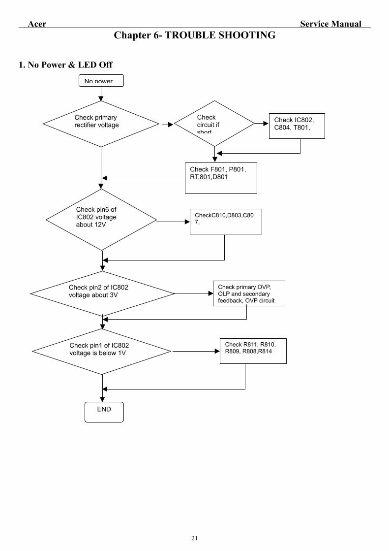
Chapter 6- TROUBLE SHOOTING 1. No Power & LED Off
No power
Check primary rectifier voltage
Check IC802, C804, T801,
Check circuit if short
Check F801, P801, RT,801,D801
Check pin6 of IC802 voltage about 12V
CheckC810,D803,C807,
Check pin2 of IC802 voltage about 3V
Check primary OVP, OLP and secondary feedback, OVP circuit
Check pin1 of IC802 voltage is below 1V
Check R811, R810, R809, R808,R814
END
21
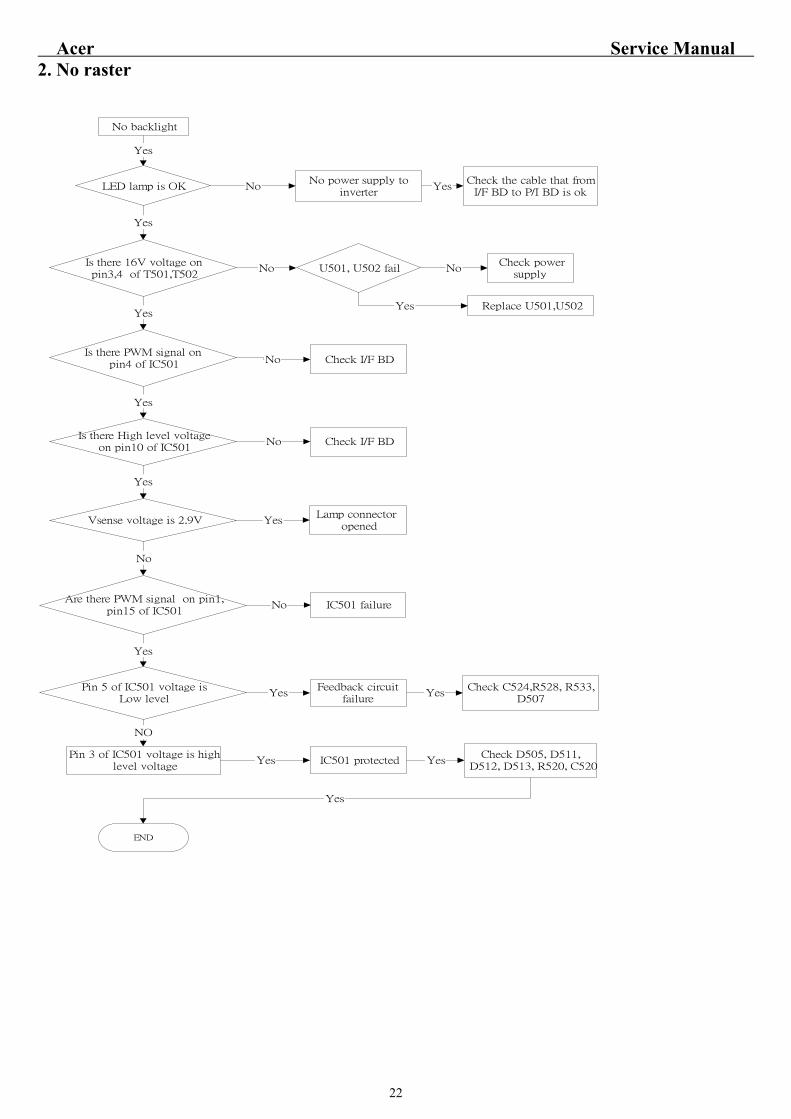
Acer Service Manual 2. No raster
No backlight
LED lamp is OK
Yes
No power supply to inverter
No
Yes
NoIs there 16V voltage on pin3,4 of T501,T502
U501, U502 fail No Check power
supply
Replace U501,U502YesYes
Is there PWM signal on pin4 of IC501 No Check I/F BD
Yes
Is there High level voltage on pin10 of IC501
No Check I/F BD
Vsense voltage is 2.9V
Yes
YesLamp connector
opened
Are there PWM signal on pin1, pin15 of IC501
No
No IC501 failure
Pin 5 of IC501 voltage is Low level
Yes
Feedback circuit failure
Yes YesCheck C524,R528, R533,
D507
NO
Pin 3 of IC501 voltage is high level voltage
Yes IC501 protected YesCheck D505, D511,
D512, D513, R520, C520
END
Yes
Check the cable that from I/F BD to P/I BD is ok
Yes
22

Acer Service Manual
3.Black screen
U105 FAIL
Black screen
Check pin4 of CN101
Check CCFL-Enable(pin 85)
of U105
Check crystal (pin 96,97) waveform of U105
Check reset (pin84) of U105
Check power supply for U105
Check power supply:pin 1,2 of
CN101
Check R167,Q106,R108,R110
Inverter Fail
Check X101,C153,C154
Check C144,R172
Check FB102,FB103,FB105,FB106
Power fail
NG
NG
NG
NG
NG
NG
YES
YES
YES
YES
YESYES
23
Acer Service Manual
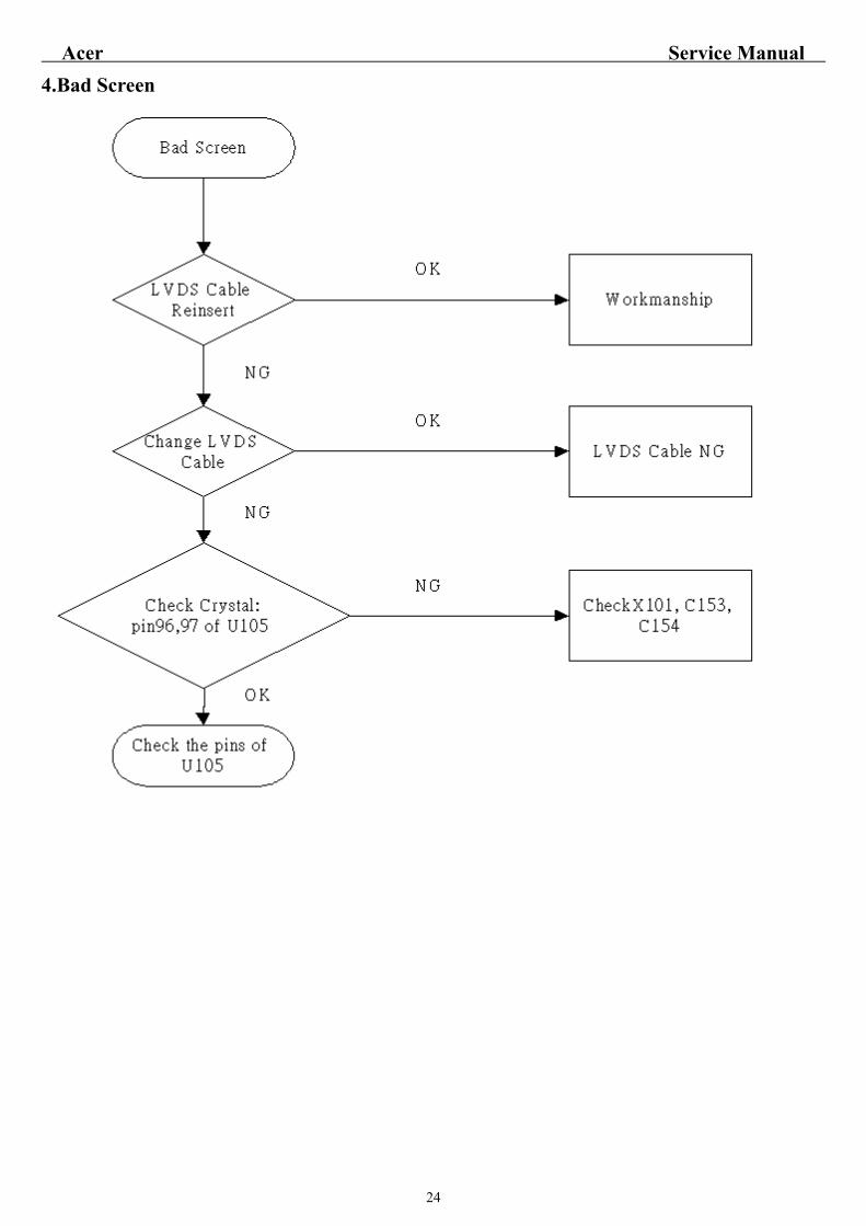
4.Bad Screen
24
Acer Service Manual 5. White screen
END
White screen
Check LVDS signal
Check Q101,Q103,Q110,
C108,C109
Check Panel-Enable of U105(pin48)
Check VLCD is 5V
Change LVDSCable
LVDS Cable Reinsert
Workmanship
Panel Fail
LVDS cable NG
U105 Fail
OK
OK
OK OK
OK
NG
NG
NG
NG
NG
25

Acer Service Manual 6.No Sound
No Sound
Re-insert or Change the Line-in Cable
Check Vs of IC 701?
Check the Input of IC 701
Check the output of IC 701
Check the Mute and Volume pins of IC 701 shorted or not?
End
Power Fail
Change IC 701
OK
NG
NG
NG
NG
OK
OK
OK
OK
26

Acer Service Manual 7. Unstable Power Unstable power
Check sampling Circuit
Check R822, R823, R824
Change R822, R823, R824
Check the R pin voltage of IC803 about 2.5V
Check R819, R820
Check R818, D804, C807 if short
Change R818, D804,
Check pin2 of IC802 voltage is 3V
Check pin1 of IC802 voltage below 1V
Change R808, R 809, R810, R 811, R815,
END
Check the C pin voltage of IC803 if 3V
Change IC803
27
Acer Service Manual
28
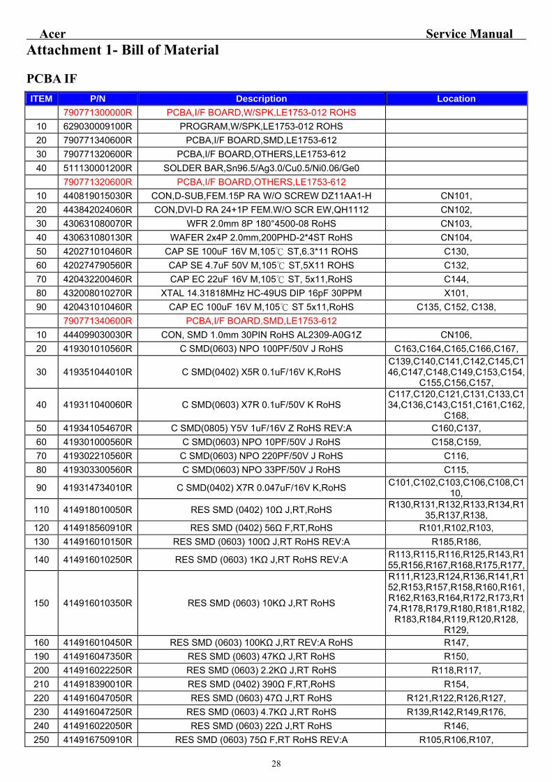
Attachment 1- Bill of Material PCBA IF ITEM P/N Description Location
790771300000R PCBA,I/F BOARD,W/SPK,LE1753-012 ROHS 10 629030009100R PROGRAM,W/SPK,LE1753-012 ROHS 20 790771340600R PCBA,I/F BOARD,SMD,LE1753-612 30 790771320600R PCBA,I/F BOARD,OTHERS,LE1753-612 40 511130001200R SOLDER BAR,Sn96.5/Ag3.0/Cu0.5/Ni0.06/Ge0
790771320600R PCBA,I/F BOARD,OTHERS,LE1753-612 10 440819015030R CON,D-SUB,FEM.15P RA W/O SCREW DZ11AA1-H CN101, 20 443842024060R CON,DVI-D RA 24+1P FEM.W/O SCR EW,QH1112 CN102, 30 430631080070R WFR 2.0mm 8P 180°4500-08 RoHS CN103, 40 430631080130R WAFER 2x4P 2.0mm,200PHD-2*4ST RoHS CN104, 50 420271010460R CAP SE 100uF 16V M,105 ST,6.3*11 ROHS C130, 60 420274790560R CAP SE 4.7uF 50V M,105 ST,5X11 ROHS C132, 70 420432200460R CAP EC 22uF 16V M,105 ST, 5x11,RoHS C144, 80 432008010270R XTAL 14.31818MHz HC-49US DIP 16pF 30PPM X101, 90 420431010460R CAP EC 100uF 16V M,105 ST 5x11,RoHS C135, C152, C138,
790771340600R PCBA,I/F BOARD,SMD,LE1753-612 10 444099030030R CON, SMD 1.0mm 30PIN RoHS AL2309-A0G1Z CN106, 20 419301010560R C SMD(0603) NPO 100PF/50V J RoHS C163,C164,C165,C166,C167,
30 419351044010R C SMD(0402) X5R 0.1uF/16V K,RoHS C139,C140,C141,C142,C145,C146,C147,C148,C149,C153,C154,
C155,C156,C157,
40 419311040060R C SMD(0603) X7R 0.1uF/50V K RoHS C117,C120,C121,C131,C133,C134,C136,C143,C151,C161,C162,
C168, 50 419341054670R C SMD(0805) Y5V 1uF/16V Z RoHS REV:A C160,C137, 60 419301000560R C SMD(0603) NPO 10PF/50V J RoHS C158,C159, 70 419302210560R C SMD(0603) NPO 220PF/50V J RoHS C116, 80 419303300560R C SMD(0603) NPO 33PF/50V J RoHS C115,
90 419314734010R C SMD(0402) X7R 0.047uF/16V K,RoHS C101,C102,C103,C106,C108,C110,
110 414918010050R RES SMD (0402) 10Ω J,RT,RoHS R130,R131,R132,R133,R134,R135,R137,R138,
120 414918560910R RES SMD (0402) 56Ω F,RT,RoHS R101,R102,R103, 130 414916010150R RES SMD (0603) 100Ω J,RT RoHS REV:A R185,R186,
140 414916010250R RES SMD (0603) 1KΩ J,RT RoHS REV:A R113,R115,R116,R125,R143,R155,R156,R167,R168,R175,R177,
150 414916010350R RES SMD (0603) 10KΩ J,RT RoHS
R111,R123,R124,R136,R141,R152,R153,R157,R158,R160,R161,R162,R163,R164,R172,R173,R174,R178,R179,R180,R181,R182,
R183,R184,R119,R120,R128, R129,
160 414916010450R RES SMD (0603) 100KΩ J,RT REV:A RoHS R147, 190 414916047350R RES SMD (0603) 47KΩ J,RT RoHS R150, 200 414916022250R RES SMD (0603) 2.2KΩ J,RT RoHS R118,R117, 210 414918390010R RES SMD (0402) 390Ω F,RT,RoHS R154, 220 414916047050R RES SMD (0603) 47Ω J,RT RoHS R121,R122,R126,R127, 230 414916047250R RES SMD (0603) 4.7KΩ J,RT RoHS R139,R142,R149,R176, 240 414916022050R RES SMD (0603) 22Ω J,RT RoHS R146, 250 414916750910R RES SMD (0603) 75Ω F,RT RoHS REV:A R105,R106,R107,

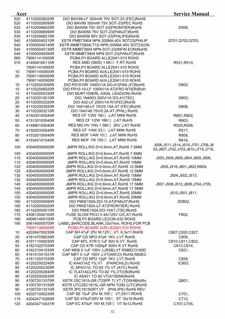
Acer Service Manual
29
260 411020026210R DIO BAV99 350mW 70V SOT-23(PHI RoHS D101,D102,D103, 260 411020026390R DIO BAV99,SOT-23(INFINEON)RoHS 260 411020026020R DIO BAV99-LF 350mW 70V SOT-23 (FEC)RoHS 260 411020026090R DIO BAV99 350mW 75V SOT-23(PEC RoHS 270 411020047210R DIO BAV70 85V SOT23 (PHILIPS) RoHS D104,D107, 270 411020047020R DIO BAV70-LF, 70V SOT-23(FEC) ROHS 280 411090005011R SCHTKY SK24A 40V/2A SMA(TSC) DO-214AC Ro D116, 280 411090005311R SCHTKY B240A 40V/2A SMA(DIODES RoHS 310 432002312144R BEAD CORE SMD(0603)120Ω 300mA SBK160808 FB104, 320 432002360012R BEAD CORE SMD(0805)60Ω 800mA GBK201209T FB105,FB106,FB107, 330 410500045210R XSTR PMBT3904 NPN 200MA,40V SOT23(PHILIP Q102,Q106, 330 410500045140R XSTR MMBT3904LT1G NPN 200MA 40V SOT23(ON 330 410500045130R XSTR MMBT3904 NPN SOT-23(INFIN EON)RoHS 330 410500045090R XSTR MMBT3904 NPN SOT-23(PANJIT)RoHS 340 410500068290R XSTR AP2305GN P-CH SOT23(APEC) RoHS Q103, 340 410500075270R XSTR AO3415 P-CH,SOT23(AOS) RoHS 340 410500044270R XSTR AO3401L P-CH(ALPHA-OMEGA) SOT23 RoH 360 410500050210R XSTR 2N7002,N-CH FET SOT-23 (PHILIPS)RoH Q105, 360 410500050130R XSTR SN7002N N-CH SOT-23(INFINEON),RoHS 360 410500050090R XSTR 2N7002 N-CH SOT-23(PANJIT)RoHS 370 410500046210R XSTR PMBT3906 PNP 200MA,40V SOT23(PHILIP Q109,Q108,Q101, 370 410500046130R XSTR MMBT3906 PNP SOT-23(INFIN EON)RoHS 370 410500046180R XSTR MMBT3906LT1G PNP 200mA 40V SOT23(ON 370 410500046090R XSTR MMBT3906 PNP SOT-23(PANJIT)RoHS 380 412000435480R IC AT24C02BN-10SU-1.8 SOIC8 2K (ATMEL)Ro U101,U102, 380 412000480280R IC M24C02-RMN6TP SO8(ST)RoHS 380 412000480990R IC CAT24C02WI-TE13 SOIC-8(CATALYST)RoHS 390 412000372020R IC LD1117AL-3.3V-A SOT-223(UTC RoHS U103, 390 412000372830R IC AS1117L-3.3TR-LF,SOT223(A1S EMI)RoHS 390 412000372070R IC AZ1117H-3.3 SOT-223(AAC)RoHS 400 412000553060R IC TSUM56AWHK-LF-1 PQFP128(MSTAR)RoHS U104, 410 412000486310R IC PM25LV010A-100SCE SOIC8(PMC)RoHS U105, 410 412000373190R IC SST25VF010A-33-4C-SAE,SOIC- 8(SST)RoH 410 412000486190R IC PS25LV010A-100SCE SOIC8(MSTAR)RoHS 420 412000279480R IC AT24C04N-10SU-2.7 SOP8 4K(A TMEL)RoHS U107, 420 412000279280R IC M24C04-WMN6TP4K SOP8 (ST) RoHS 420 412000479990R IC CAT24C04WI-TE13 SOIC-8(CATALYST)RoHS
430 411131562950R ZENER 6.2V BZT52C6V2-7-F SOD-123(DIODES) ZD101,ZD102,ZD103,ZD104,ZD105,ZD106,ZD107,ZD108,ZD109,
430 411121462950R ZENER 6.2V BZT52-C6V2 SOD-123(WILLAS)ROH 430 411130962950R ZENER 6.2V MMSZ5234B SOD-123(PANJIT)RoH 440 506140005700R LABEL,BARCODE,BLANK,33x7mm, ROHS,FOR PCB 460 432002330040R BEAD CORE SMD(0603) 30Ω 500mA HB-1H1608 FB101,FB102,FB103, 470 412000330020R IC LD1117AL-1.8V-A SOT223(UTC) RoHS U108, 470 412000330070R IC AZ1117H-1.8 SOT223(AAC)RoHS 470 412000330830R IC AS1117L-1.8/TR-LF,SOT223(A1 SEMI)RoHS 480 414916033150R RES SMD (0603) 330Ω J,RT RoHS R187,R188, 490 414916010050R RES SMD (0603) 10Ω J,RT RoHS R159,R165, 500 490481300600R PCB,I/F BOARD,LE1753-X12 510 412000531061R IC CAT24C08WI-H-RECV SOIC-8(Mstar)RoHS U106, 510 412000531060R IC CAT24WC08W-H-RECV for HDCP(Mstar) R

Acer Service Manual
30
520 414918010150R RES SMD (0402) 100Ω J,RT,RoHS R108,R109,R110, 530 419341054660R C SMD(0603) Y5V 1uF/16V Z,RoHS C150, 540 414916020350R RES SMD (0603) 20KΩ J,RT RoHS REV:A R151, 550 511130002200R SOLDER PASTE,Sn96.5-Ag3.0-Cu0.5 ROHS 550 511130002201R SOLDER PASTE,Sn96.5%Ag3.0%Cu0.5% 550 511130002202R SOLDER PASTE,Sn95.5%Ag3.9%Cu0.6%
PCBA PI ITEM P/N Description Location
790931400500R PCBA,P/I BOARD,LE2018-522 ROHS 10 430300800660R HRN ASS'Y 8P 80mm UL1007#24,RoHS CN801, 20 430637020030R WFR. 2P P=3.5mm 90°W/LOCK,RoHS CN501,CN502,CN503,CN504, 30 430631040080R WFR. 4P 2.0mm R/A HF5604E RoHS CN701, 40 426000090800R XFMR SW DIP 142uH EEL19 SPW-080,ROHS T501,T502, 50 416202223610R CAP MEY 2200pF 250V M Y2 Y5V P=7.5mm RoH C801,C802, 60 416194743011R CAP MEX 0.47uF 275V K X2,F15 RoHS C803, 70 420431514280R CAP SEK 150uF/420V M,105 CF 18x40,RoHS C804, 80 416202224610R CAP MEY 2200pF 400V M Y,F10mm RoHS C805,
100 418247233020R CAP CD X7R 4700pF 1KV K,W/O FO RMING,RoH C806, 110 418110058560R CAP CD SL 10pF 3KV J,ST,RoHS CC45SL3FD10 C506,C523, 120 418103051910R CAP CD NPO 3pF 3KV D,F7.5, RoHS C528,C509, 130 420421020211R CAP SD 1000uF 25V M,105 F 13x20 RoHS C815, 140 420424710260R CAP SD 470uF/25V M 105 ST 10x16,RoHS C501,C817,C702, 150 420421020102R CAP EC 1000uF/10V M,105 N-F 10x16(L-ES C818, 160 430613420290R FUSE SLOW 2,250,Axial Lead,3.6 x10mm RoH F801, 170 412140001390R IC EL817M-B(EVERLIGHT)RoHS IC801, 170 412140002380R IC LTV817M-PR VDE (LITE-ON) P=10mm RoHS 180 425000010670R COIL CHK 20mH UU16 CHK-067,RoH S,UF2324S L801, 190 425000010530R COIL CHK 5uH 7.8X10 CHK-053 0 181085R0L L802,L803, 200 440149000220R SKT AC 10A/250V U/C/V,G/Y=45mm TU-301-SP P801, 210 442299001130R CON PHONE JACK GREEN R/A 1P PB J303-2-A P701, 220 432009400701R NTC 5Ω 4A 10ψ P=5mm, F RoHS RT801, 230 415350208550R RES MOF 2W 0.2Ω J,MINI,HK15 RoHS R805, 240 426000090790R XFMR SW DIP 550uH SPW-079,ROHS T801, 250 411050005020R DIO BRDG BL4-06-BF52-LF 600V/4A(FRONTIER D801, 250 411050005090R DIO BRDG FL406 600V/4A(PEC)RoH S 250 411050007010R DIO BRDG KBL405G 600V/4A(TSC) RoHS 260 502040604500R SHIELD EMI LE1915 ROHS H501, 270 735100008600R ASSY,H/S,TDA8496L-J-15-B-T,LE1753 280 790911440500R PCBA,P/I BOARD SMD,LE2041-510 ROHS 290 735100008800R ASSY,H/S,SRF10100/SRF1050,LE2041 ROHS 300 735100007900R ASSY,H/S,AP2761I-A,LE1936 310 410050062330R XSTR AF4971NN N-CH PDIP8(ANACH IP)RoHS U501,U502, 310 410500071290R XSTR AP9971GD,N-CH,PDIP-8(APEC RoHS 320 511130001200R SOLDER BAR,Sn96.5/Ag3.0/Cu0.5/Ni0.06/Ge0 330 511110000101R HOT-MELT ADHESIVES (#526) 340 511110000501R SILICONE RTV RUBBER,UB-511(EURO) 350 416204724610R CAP MEY 4700pF 400V M Y,F10mm RoHS C823-1, 360 418210133030R CAP CD X7R 100pF 1KV K VT RoHS C808,
735100007900R ASSY,H/S,AP2761I-A,LE1936 10 410500059290R XSTR AP2761I-A N-CH TO-220CFM ADVANCED P Q804, 10 410050060130R XSTR SPA06N80C3 N-CH PG-TO220- 3-31(INFI 10 410050059240R XSTR FQPF7N80C N-CH TO220F(FAI RCHILD)Ro 20 507200003700R HEATSINK,46x20xt10mm LE1704/05 30 509112306100R SCREW,P,CROSS,T.T-3*6,ZnROHS
735100008600R ASSY,H/S,TDA8496L-J-15-B-T,LE1753 10 412000526020R IC TDA8496L-J-15-B-T HZIP-15B(UTC)RoHS U701, 20 507200004900R HEATSINK,35x20xt10mm, LE1753 30 509142308101R SCREW,P,CROSS,W/WAS(8mm),T.T-3*8,Zn ROHS
735100008800R ASSY,H/S,SRF10100/SRF1050,LE2041 ROHS 10 411090023040R SCHTKY SRF10150C 150V/10A ITO2 20(MOSPEC D804, 10 411090023020R SCHTKY SRF10-15CT-LF 150V/10A( FEC)RoHS

Acer Service Manual
31
10 411090023090R SCHTKY SB10150FCT 150V/10A ITO 220AB(PAN 20 411090024480R SCHTKY SP1040C 40V/10A ITO220(WILLAS)RoH D805, 20 411090040010R SCHTKY SRF1050 50V/10A ITO220AB(TSC)RoHS 30 507200005300R HEATSINK,75x25xt15mm, LP2610 40 509112306100R SCREW,P,CROSS,T.T-3*6,ZnROHS
790911440500R PCBA,P/I BOARD SMD,LE2041-510 ROHS 10 412000495840R IC NCP1337DR2G SOIC-7(ON)RoHS IC802, 20 414904010050R RES SMD (1206) 10Ω J,RT RoHS R827,R828, 30 414916010150R RES SMD (0603) 100Ω J,RT RoHS REV:A R713, 40 414916010250R RES SMD (0603) 1KΩ J,RT RoHS REV:A R706,R707, 50 414908010250R RES SMD (0805) 1KΩ J,RT RoHS REV:A R813,R819,R820,R821, 60 414916100210R RES SMD (0603) 10KΩ F,RT RoHS R513,R537,R538,R702,R701,R703,70 414908010350R RES SMD (0805) 10KΩ J,RT RoHS REV:A R812,R829,R830, 80 414916100310R RES SMD (0603) 100KΩ F,RT RoHS R501,R520, 90 414916010550R RES SMD (0603) 1MΩ J,RT RoHS REV:A R526,R519,
100 414916110310R RES SMD (0603) 110KΩ F,RT RoHS REV:A R512, 110 414908120210R RES SMD (0805) 12K F RT RoHS REV:A R815, 120 414916015050R RES SMD (0603) 15Ω J,RT RoHS REV:A R534,R535, 130 414916020150R RES SMD (0603) 200Ω J,RT RoHS R527,R524, 140 414908020150R RES SMD (0805) 200Ω J,RT RoHS R817, 150 414916020250R RES SMD (0603) 2KΩ J,RT RoHS R710,R709, 160 414908033050R RES SMD (0805) 33Ω J,RT RoHS R504,R505,R530,R532, 170 414908300110R RES SMD (0805) 3KΩ F,RT RoHS REV R824, 180 414916030350R RES SMT(0603)30KΩ J,RT RoHS R714,R705, 190 414916750110R RES SMD (0603) 7.5KΩ F,RT RoHS R533,R536, 200 414916330410R RES SMD (0603) 3.3M F RT RoHS R507, 210 414916470010R RES SMD (0603) 470Ω F,RT RoHS R528,R523,R521,R529, 230 414916047250R RES SMD (0603) 4.7KΩ J,RT RoHS R708, 240 414908510110R RES SMD (0805) 5.1KΩ F,RT RoHS R822, 250 414916470210R RES SMD (0603) 47KΩ F,RT RoHS R514,R704, 260 414908470210R RES SMD (0805)47KΩ F,RT,RoHS R823, 270 414916470310R RES SMD (0603) 470KΩ F,RT ROHS R518, 280 414916510110R RES SMD (0603) 5.1KΩ F,RT RoHS R539, 290 414916430210R RES SMD (0603) 43KΩ F,RT,RoHS R508, 300 414908047450R RES SMD (0805) 470KΩ J,RT RoHS R808,R809,R810,R811, 310 414916056250R RES SMD (0603) 5.6KΩ J,RT ROHS REV:A R712,R711, 320 414916604310R RES SMD (0603) 604KΩ F,RT RoHS R516, 340 414908750010R RES SMD (0805)750Ω F,RT,RoHS R807,R831,R832,
350 419311040060R C SMD(0603) X7R 0.1uF/50V K RoHS C503,C518,C519,C520,C825,C709,C703,
360 419311020060R C SMD(0603) X7R 1000PF/50V K RoHS C510,C516, 370 419311020070R C SMD(0805) X7R 1000PF/50V K RoHS C504,C505,C522,C529, 380 419302210360R C SMD(0603) NPO 220PF/50V G RoHS C812, 390 419312220060R C SMD(0603) X7R 2200PF/50V K RoHS C517,C524,C530, 400 419312220070R C SMD(0805) X7R 2200PF/50V K RoHS C525,C513, 410 419312233060R C SMD(0603) X7R 0.022uF/25V K RoHS C511, 420 419342254670R C SMD(0805) Y5V 2.2uF/16V Z RoHS C507,C515, 420 419352254070R C SMD(0805) X5R 2.2uF/16V K, RoHS 430 419342253670R C SMD(0805) Y5V 2.2uF/25V Z RoHS C502, 440 419312720070R C SMD (0805) X7R 2700pF 50V K ROHS C514,C527, 450 419303310560R C SMD(0603) NPO 330PF/50V J RoHS C512, 460 419314720060R C SMD(0603) X7R 4700PF/50V K RoHS C710,C711, 470 419314744060R C SMD(0603) X7R 0.47uF/16V K,RoHS C704,C706, 480 419301510560R C SMD(0603) NPO 150PF/50V J RoHS C521, 490 411100912020R ZENER 12V MMSZ5242A SOD123(PEC RoHS ZD803, 490 411131512052R ZENER 12V 0.5W DDZ12C-F,SOD123 (DIODES)R 490 411131412020R ZENER 12V MMSZ5242A SOD-123(WILLAS)ROHS 500 412000455630R IC OZ9938GN SOIC16(O2 MICRO)RoHS IC501, 510 411023004021R DIO SN4148-LF 75V/0.15A SMD 1206 (FEC)Ro D501,D505,D511,D512, 510 411020046090R DIO 1N4148W 75V/0.15A(PEC)RoHS SOD-123 510 411020046310R DIO 1N4148W-F 75V/0.15A(DIODES RoHS,SOD- 520 411020026210R DIO BAV99 350mW 70V SOT-23(PHI RoHS D502,D503,D504,D507,D508,D509,520 411020026390R DIO BAV99,SOT-23(INFINEON)RoHS
Acer Service Manual
32
520 411020026020R DIO BAV99-LF 350mW 70V SOT-23 (FEC)RoHS 520 411020026090R DIO BAV99 350mW 75V SOT-23(PEC RoHS 530 411020068020R DIO BAW56 70V SOT-23(FRONTIER)RoHS D506, 530 411020068090R DIO BAW56 75V SOT-23(PANJIT)RoHS 530 411020068210R DIO BAW56 85V SOT-23(PHILIPS)RoHS 540 410500045210R XSTR PMBT3904 NPN 200MA,40V SOT23(PHILIP Q701,Q702,Q703, 540 410500045140R XSTR MMBT3904LT1G NPN 200MA 40V SOT23(ON 540 410500045130R XSTR MMBT3904 NPN SOT-23(INFIN EON)RoHS 540 410500045090R XSTR MMBT3904 NPN SOT-23(PANJIT)RoHS 560 790911410500R PCBA,P/I BOARD AI,LE2041-510 ROHS 570 414908160110R RES SMD (0805) 1.6KΩ F,RT,RoHS R531,R510,
790911410500R PCBA,P/I BOARD AI,LE2041-510 ROHS 10 790911450500R PCBA,P/I BOARD AI/A,LE2041-510 ROHS 20 790911460500R PCBA,P/I BOARD AI/R,LE2041-510 ROHS
790911450500R PCBA,P/I BOARD AI/A,LE2041-510 ROHS 10 411020053090R DIO PS1010R 1000V/1A DO-41(PAN JIT)RoHS D802, 10 411032006020R DIO FR10-10-LF 1000V/1A AT(FRO NTIER)RoH 10 411020055330R DIO MUR1100ERL AXIAL LEAD(ON) RoHS 20 411022010010R DIO 1N4003 200V/1A DO-41(TSC) D803, 20 411020052020R DIO A02-LF 200V/1A R1(FEC)RoHS 30 411022003020R DIO 1N4148-LF 75V/0.15A AT (FEC)RoHS D806, 30 411022003210R DIO 1N4148 75V/0.2A AT (PHIL) RoHS 40 415030105540R RES CF 1/2W 1MΩ J,AT MINI RoHS R801,R802, 50 415130183540R RES CF 1/2W 18KΩ J,AT,RoHS R803, 60 414880155540R RES MG HV 1Ws 1.5MΩ 2KV J,AT RoHS R525,R506, 70 415020330540R RES CF 1/4W 33Ω J,AT MINI RoHS R517, 80 415320100540R RES MOF 1/4W 10Ω J,AT MINI RoHS R806, 90 415340101540R RES MOF 1W 100Ω J,AT MINI RoHS R816,
100 430405000000R JMPR ROLL/KG D=0.6mm,AT,RoHS 7.5MM J506,J511,J514,J515,J701,J706,J803,J807,J702,J703,J810,J715,J716,
100 430405000000R JMPR ROLL/KG D=0.6mm,AT,RoHS 7.5MM 110 430405000000R JMPR ROLL/KG D=0.6mm,AT,RoHS 10MM J503,J509,J809,J804,J805,J806, 110 430405000000R JMPR ROLL/KG D=0.6mm,AT,RoHS 10MM 120 430405000000R JMPR ROLL/KG D=0.6mm,AT,RoHS 12.5MM J505,J516,J801,J802,R804, 120 430405000000R JMPR ROLL/KG D=0.6mm,AT,RoHS 12.5MM 130 430405000000R JMPR ROLL/KG D=0.6mm,AT,RoHS 15MM J504,J502,J513, 130 430405000000R JMPR ROLL/KG D=0.6mm,AT,RoHS 15MM 140 430405000000R JMPR ROLL/KG D=0.6mm,AT,RoHS 17.5MM J507,J508,J512,J808,J704,J705, 140 430405000000R JMPR ROLL/KG D=0.6mm,AT,RoHS 17.5MM 150 430405000000R JMPR ROLL/KG D=0.6mm,AT,RoHS 20MM J510,J501,J811, 150 430405000000R JMPR ROLL/KG D=0.6mm,AT,RoHS 20MM 160 411020050090R DIO P6KE150A,DO-15,AT(PANJIT)RoHS ZD802, 160 411020050020R DIO P6KE150A-LF AT(FRONTIER) RoHS 160 411020050010R DIO P6KE150A,DO-15AT,(TSC)RoHS 170 430613040100R FUSE SLOW PICO II 4A/125V U/C,AT,RoHS F802, 180 490901400100R PCB,P/I BOARD,LE2239-X32 ROHS 190 506140005700R LABEL,BARCODE,BLANK,33x7mm, ROHS,FOR PCB
790911460500R PCBA,P/I BOARD AI/R,LE2041-510 ROHS 10 420264700230R CAP SH 47uF 25V M,125,VT, 6.3x11,RoHS C807,C820,C827, 20 418147038530R CAP CD NPO 47pF 1KV J,VT RoHS C809, 40 419111040030R CAP MTL X7R 0.1uF 50V K,VT, RoHS C810,C811,C822, 50 418210227030R CAP CD X7R 1000pF 500V K VT RoHS C813,C814, 60 416231041530R CAP MEB 0.1uF 100V J,(RSB),VT RSBEC3100D C821, 60 416141041531R CAP MKT 0.1uF 100V J,VT(ARCO) RoHS,R82EC 70 418112031530R CAP CD NPO 12pF 1KV J,VT,RoHS C826, 80 412022002240R IC KA431AZ 1%,VT (FAIRCHILD) RoHS IC803, 80 412022002300R IC AP431VL TO-92 1% VT (ATC) RoHS 80 412022002840R IC TL431ACLPG TO-92 1%,VT(ON)RoHS 80 412022002830R IC AS431 TO-92 VT(A1SEMI)RoHS 90 410072013370R XSTR 2SC1815-GR (T2SPF.T) VT (TOSHIBA)Ro Q801, 90 410072013150R XSTR UTC2SC1815L-GR NPN TO92 (UTC)RoHS 90 410072013210R XSTR 2PC1815GR*I VT (PHILIPS) RoHS REV:
100 420271000230R CAP SE 10uF 25V M,105 VT,5X11 ROHS C701, 110 420424710260R CAP SD 470uF/25V M 105 ST 10x16,RoHS C712, 120 420434710431R CAP EC 470uF 16V M,105 VT 8x12,RoHS C707,C705,
Acer Service Manual
33
130 420262210460R CAP SH 220uF 16V M,125,ST,10x13,RoHS C708, 140 432002200200R FERR BEAD 3.5x6x0.65,VT,RoHS FB801,
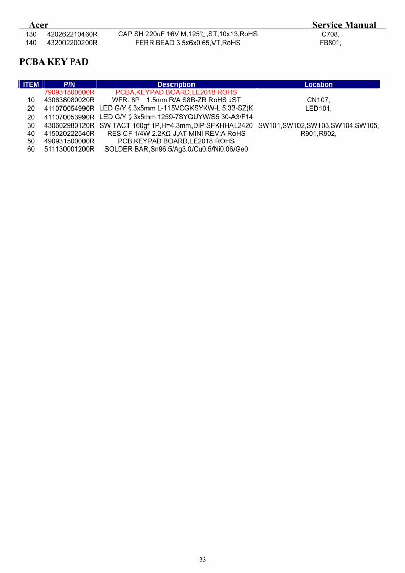
PCBA KEY PAD ITEM P/N Description Location
790931500000R PCBA,KEYPAD BOARD,LE2018 ROHS 10 430638080020R WFR. 8P 1.5mm R/A S8B-ZR RoHS JST CN107, 20 411070054990R LED G/Y∮3x5mm L-115VCGKSYKW-L 5.33-SZ(K LED101, 20 411070053990R LED G/Y∮3x5mm 1259-7SYGUYW/S5 30-A3/F14 30 430602980120R SW TACT 160gf 1P,H=4.3mm,DIP SFKHHAL2420 SW101,SW102,SW103,SW104,SW105,40 415020222540R RES CF 1/4W 2.2KΩ J,AT MINI REV:A RoHS R901,R902, 50 490931500000R PCB,KEYPAD BOARD,LE2018 ROHS 60 511130001200R SOLDER BAR,Sn96.5/Ag3.0/Cu0.5/Ni0.06/Ge0

Acer Service Manual
Attachment 2- Schematic
34
Acer Service Manual
35

Acer Service Manual
36

Acer Service Manual
37
Acer Service Manual
38

Acer Service Manual
39
Top Related