


Languages
Pages
Legal

University of KaiserslauternDepartment of Computer ScienceDatabase and Information Systems
SeminarRecent Trends inDatabase Research
Summer Semester 2013
Inhaltverzeichnis
1 Einleitung . . . . . . . . . . . . . . . . . . . . . . . . . . . . . . . . . . . . . . . . . . . . . . . . . . . . . . . 32 Was ist Phase-change Memory (PCM)? . . . . . . . . . . . . . . . . . . . . . . . . . . . . . . 43 Einordnung in bekannte Speicher . . . . . . . . . . . . . . . . . . . . . . . . . . . . . . . . . . . 44 Vor- und Nachteile von PCM, vorstellbare Architekturen . . . . . . . . . . . . . . . 65 Lindern der Nachteile . . . . . . . . . . . . . . . . . . . . . . . . . . . . . . . . . . . . . . . . . . . . . . 6
5.1 Data-Comparison Write Scheme . . . . . . . . . . . . . . . . . . . . . . . . . . . . . . . . 65.2 Seitenersetzungsstrategien . . . . . . . . . . . . . . . . . . . . . . . . . . . . . . . . . . . . . 75.3 Probabilistischer Record-Swapping-Algorithmus . . . . . . . . . . . . . . . . . . 8
6 PCMLogging . . . . . . . . . . . . . . . . . . . . . . . . . . . . . . . . . . . . . . . . . . . . . . . . . . . . . 96.1 Datenstrukturen und Grundlagen . . . . . . . . . . . . . . . . . . . . . . . . . . . . . . 96.2 Vorgehen auf Seitenebene . . . . . . . . . . . . . . . . . . . . . . . . . . . . . . . . . . . . . 116.3 Vorgehen auf Satzebene . . . . . . . . . . . . . . . . . . . . . . . . . . . . . . . . . . . . . . . 126.4 Performance-Aspekte . . . . . . . . . . . . . . . . . . . . . . . . . . . . . . . . . . . . . . . . . 14
7 Fazit . . . . . . . . . . . . . . . . . . . . . . . . . . . . . . . . . . . . . . . . . . . . . . . . . . . . . . . . . . . . 15
Die Verwendung von Phase-change Memory inmodernen DBMS-Architekturen
Jan Philipp Starz
University of Kaiserslautern
Abstract. Die folgende wissenschaftliche Arbeit behandelt Phase-changeMemory (PCM) und dessen moglichen Einsatz in modernen DBMS-Architekturen.
Der erste Teil dieser Arbeit beschaftigt sich grundlegend mit PCM. Dabeiwird zu Anfang dessen Funktionsweise erlautert sowie eine kurze Einord-nung in bekannte Speicher gegeben. Im weiteren Verlauf werden die Vor-und Nachteile von PCM und denkbare Speicherarchitekturen vorgestellt.Darauf aufbauend folgen Strategien, die einen geringeren Verschleiß vonPCM-Modulen erzielen.
Im zweiten Teil wird das DBMS-Logging-Schema PCMLogging vorgestellt,welches eine mogliche Verwendung von PCM aufzeigt, das Transaktions-Logging und die Recovery-Performance zu optimieren. Dabei werden diebenotigten Datenstrukturen sowie das Vorgehen auf Seiten- und Satzebenebehandelt. Auf die Perfomance-Aspekte von PCMLogging wird ebenfallsnaher eingegangen.
Abschließend werden ein Fazit gezogen und ein Blick in die Zukunft vonPCM und dessen Bedeutung fur kommende Datenbanksysteme gegeben.
1 Einleitung
Um Mehrkernprozessoren mit Multi-Threading-Technologie voll ausschopfen undgroße Arbeitsauftrage optimal parallelisieren zu konnen, benotigen wir zunehmendgroßeren Arbeitsspeicher. Durch die beschrankte Skalierbarkeit von DRAM ist mandaher gezwungen, eine Alternative zu finden, die DRAM in ihrem Laufzeitverhaltenahnelt und skalierbar ist.Phase-change Memory scheint hierfur ein moglicher Kandidat zu sein. Auch wenner einige Vorteile, wie geringe Zugriffslatenzen, Skalierbarkeit und persistente Spei-cherung vereint, uberwiegt dennoch der Nachteil der niedrigen Lebensdauer einerPCM-Zelle. Um PCM also praktikabel nutzen zu konnen, gilt es den Verschleiß sostark einzudammen, dass er sich mit heutzutage gebrauchlichen Speichern messenkann. Dies ist das Ziel vom Data-Comparison Write (DCW) Scheme [3], den Seiten-ersetzungsstrategien least wear-unit difference (LWD), least page wear (LPW) undleast frequently modified (LFM) [2] und dem probabilistischen Record-Swapping-Algorithmus [1].
In einer Zeit, in der immer mehr und großere Datenmengen verwaltet werdenmussen, sind auch Datenbankforscher auf die attraktiven Vorteile von PCM aufmerk-sam geworden, die sich von neuartigen Datenbanksystemen mit integriertem PCMPerformance-Gewinne erhoffen. So sollen beispielsweise Anfragen schneller abgewick-elt oder der Recovery-Prozess beschleunigt werden, um zum einen die Mehrbe-nutzbarkeit zu steigern und zum anderen den Schaden durch Systemausfalle zuminimieren. Eine Moglichkeit stellt das PCMLogging dar, welches PCM zur DRAM-Unterstutzung zwischen Prozessor und externem Speicher einsetzt, um so die Nicht-Volatilitat und die schnelle Zugriffsgeschwindigkeit des PCM auszunutzen [1].

4
2 Was ist Phase-change Memory (PCM)?
Phase-Change Memory (PCM) ist ein neuartiger Speicher, der anstelle eines Kon-densators – wie bei herkommlichen DRAM – ein Phasenwechselmaterial zur Daten-speicherung besitzt. Als Phasenwechselmaterial wird eine Germanium-Antimon-Tellur-Verbindung (Ge2Sb2Te5, kurz GST) verwendet, die je nach Beschaffenheiteinen Datenwert speichert. Liegt das GST kristallin vor, so befindet sich die PCM-Zelle im SET-Zustand. In diesem Zustand weist das GST einen niedrigen elek-trischen Widerstand auf, woraus eine logisch gespeicherte ’1’ folgt. Ist das GSThingegen im amorphen RESET-Zustand, besitzt es einen hohen elektrischen Wider-stand, woraus eine logische ’0’ gelesen werden kann. Um eine PCM-Zelle in denZustand SET zu versetzen, erhalt die Zelle uber einen langeren Zeitraum mode-rate elektrische Impulse. Kontrar dazu ist der RESET-Zustand. Dieser wird her-beigefuhrt, indem man das Phasenwechselmaterial mit kurzen, hoch energetischenImpulsen wieder amorph schmilzt. Das Lesen der gespeicherten Daten geschiehtdurch das Messen des elektrischen Widerstands des Materials und benotigt somitnur wenig Energie [5]. Die wesentlichen Unterschiede der drei Operationen SET,RESET und READ werden in Abbildung 1 verdeutlicht.Dadurch, dass zur Aufrechterhaltung des jeweiligen Zustands (kristallin oder amorph)kein elektrischer Strom benotigt wird, ist PCM ein nicht-volatiler Speicher. Außer-dem ist PCM byte-adressierbar und ermoglicht die Anderung einzelner Bits, indemdie jeweilige PCM-Zelle gesondert angesprochen wird [1]. Die Lebensdauer einerPCM-Zelle ist jedoch beschrankt, da jede auf sie angewendete Operation unweiger-lich zum Zerfall des Phasenwechselmaterials fuhrt [5].
Table 1: Comparison of memory technologies.DRAM PCM NAND Flash HDD
Read energy 0.8 J/GB 1 J/GB 1.5 J/GB [28] 65 J/GBWrite energy 1.2 J/GB 6 J/GB 17.5 J/GB [28] 65 J/GBIdle power ∼100 mW/GB ∼1 mW/GB 1–10 mW/GB ∼10 W/TBEndurance ∞ 106 − 108 104 − 105 ∞Page size 64B 64B 4KB 512BPage read latency 20-50ns ∼ 50ns ∼ 25 µs ∼ 5 msPage write latency 20-50ns ∼ 1 µs ∼ 500 µs ∼ 5 msWrite bandwidth ∼GB/s per die 50-100 MB/s per die 5-40 MB/s per die ∼200MB/s per driveErase latency N/A N/A ∼ 2 ms N/ADensity 1× 2− 4× 4× N/ANote: The table contents are based mainly on [10, 15, 22].
"RESET" pulse
"SET" pulse
READ
Time
(Te
mp
era
ture
)C
urr
en
t
cryst
melt
T
T
Figure 1: Currents and timings (not to scale) forSET, RESET, and READ operations on a PCM cell.For phase change material Ge2Sb2Te5, Tmelt ≈ 610◦Cand Tcryst ≈ 350◦C.
the primary main memory, and the key challenge of over-coming its write limitations.
2.1 PCM TechnologyPhase change memory (PCM) is a byte-addressable non-
volatile memory that exploits large resistance contrast be-tween amorphous and crystalline states in so-called phasechange materials such as chalcogenide glass. The differencein resistance between the high-resistance amorphous stateand the low-resistance crystalline state is typically aboutfive orders of magnitude and can be used to infer logicalstates of binary data (high represents 0, low represents 1).Programming a PCM device involves application of elec-
tric current, leading to temperature changes that either SETor RESET the cell, as shown schematically in Figure 1. ToSET a PCM cell to its low-resistance state, an electricalpulse is applied to heat the cell above the crystalization tem-perature Tcryst (but below the melting temperature Tmelt) ofthe phase change material. The pulse is sustained for a suffi-ciently long period for the cell to transition to the crystallinestate. On the other hand, to RESET the cell to its high-resistance amorphous state, a much larger electrical currentis applied in order to increase the temperature above Tmelt.After the cell has melted, the pulse is abruptly cut off, caus-ing the melted material to quench into the amorphous state.To READ the current state of a cell, a small current thatdoes not perturb the cell state is applied to measure theresistance. At normal temperatures (< 120◦C ≪ Tcryst),PCM offers many years of data retention.
2.2 Using PCM in the Memory HierarchyTo see where PCM may fit in the memory hierarchy, we
need to know its properties. Table 1 compares PCM withDRAM (technology for today’s main memory), NAND flash
SSD/HARD DISK
ME
MO
RY
MA
INCACHE
PCM
CPU(a)
CACHE
SSD/HARD DISK
CPU
DRAM PCM
(b)
CACHE
SSD/HARD DISK
DRAM CACHE
CPU
PCM
(c)
Figure 2: Candidate main memory organizationswith PCM.
(technology for today’s solid state drives), and HDD (harddisk drives), showing the following points:
• Compared to DRAM, PCM’s read latency is close tothat of DRAM, while its write latency is about anorder of magnitude slower. PCM offers a density ad-vantage over DRAM. This means more memory capac-ity for the same chip area, or potentially lower priceper capacity. PCM is also more energy-efficient thanDRAM in idle mode.
• Compared to NAND Flash, PCM can be programmedin place regardless of the initial cell states (i.e., with-out Flash’s expensive “erase” operation). Therefore,its sequential and random accesses show similar (farsuperior) performance. Moreover, PCM has orders ofmagnitude higher write endurance than Flash.
Because of these attractive properties, PCM is being incor-porated in mobile handsets [24], and recent computer ar-chitecture and systems studies have argued that PCM is apromising candidate to be used in main memory in futuremainstream computer systems [9, 15, 22].
Figure 2 shows three alternative proposals in recent stud-ies for using PCM in the main memory system [9, 15, 22].Proposal (a) replaces DRAM with PCM to achieve largermain memory capacity. Even though PCM is slower thanDRAM, clever optimizations have been shown to reduce ap-plication execution time on PCM to within a factor of 1.2of that on DRAM [15]. Both proposals (b) and (c) includea small amount of DRAM in addition to PCM so that fre-quently accessed data can be kept in the DRAM buffer toimprove performance and reduce PCM wear. Their differ-ence is that proposal (b) gives software explicit control of theDRAM buffer [9], while proposal (c) manages the DRAM
22
Abbildung 1. Energieaufwand fur die PCM-Operationen SET, RESET und READ. FurGST ist Tmelt ≈ 610◦C und Tcryst ≈ 350◦C [5]
3 Einordnung in bekannte Speicher
Ein Vergleich von PCM mit heute gebrauchlichen Speichern verdeutlicht das Po-tential dieser Technologie.
PCM erreicht eine zwei- bis vierfach hohere Dichte als DRAM und hat damitgegebenenfalls einen gleich hohen Wert wie NAND Flash. Eine PCM-Zelle kannursprunglich nur ein Bit speichern, jedoch existiert bereits ein Prototyp, der zweiBits pro Zelle (4 logische Zustande) verkorpert. Dieser Prototyp arbeitet mit zweiZwischenphasen des Phasenwechselmaterials, deren Widerstande zwischen den bei-den Extremwerten liegen [5].Die Leselatenz von PCM liegt mit ca. 50ns sehr nahe an der von DRAM und istdamit deutlich besser als die von NAND Flash. Erreicht wird dieser Wert durch

5
DRAM NAND Flash HDD PCMDichte 1X 4X N/A 2-4XLeselatenz (Seitengröße)
20-50ns (64B)
~25µs (4KB)
~5ms (512B)
~50ns (64B)
Schreiblatenz (Seitengröße)
20-50ns (64B)
~500µs (4KB)
~5ms (512B)
~1µs (64B)
Idle-Verbrauch ~100 mW/GB 1-10 mW/GB ~10 W/TB ~1 mW/GBRead-Verbrauch 0.8 J/GB 1.5 J/GB 65 J/GB 1 J/GBWrite-Verbrauch 1.2 J/GB 17.5 J/GB 65 J/GB 6 J/GBBeständigkeit (in Schreibzyklen) N/A 104-105 ∞ 106-108
Abbildung 2. Vergleich heutiger Speichertechnologien [1][5]
die kurze, energiearme Ansteuerung der PCM-Zellen, um deren Widerstand zu er-mitteln. So ist es auch nicht verwunderlich, dass der Energieverbrauch einer PCM-Read-Operation nur 0.2 J/GB hoher ist.Eine im Vergleich zu DRAM hohe und zu NAND Flash niedrige Schreiblatenz lasstsich durch den Zeitaufwand der SET-Operation erklaren. PCM ist byte-adressierbarund muss somit nicht wie Flashspeicher den gesamten Block zurucksetzen, in denDaten geschrieben werden sollen [3]. Daraus resultiert auch der merkliche Un-terschied zwischen 6 und 17.5 J/GB fur eine Write-Operation. Die Energiedif-ferenz zwischen DRAM und PCM von 4.8 J/GB liegt in der Umsetzung der Write-Operation einer PCM-Zelle. Ihr Verbrauch variiert im Falle des Data-ComparisonWrite (DCW) Scheme (siehe Kapitel 5.1) zwischen viel zugefuhrter Energie inkurzer Zeit (RESET-Operation), maßiger Energiezufuhr uber langere Zeit (SET-Operation) und sehr wenig Energieverbrauch (READ-Operation).Der Verbrauch im Idle-Zustand von ca. 1 mW/GB wird mithilfe des Phasenwechsel-materials erreicht, welches persistentes Schreiben ermoglicht. Damit liegt PCM weitunter dem Idle-Energieverbauch von DRAM und kann sich mit dem Verbrauchs-bestwert von NAND-Flashspeichern messen.Die Lebensdauer des Phasenwechselmaterials ist bisher ein großer Schwachpunkt derPCM-Technologie. Da sich gegenwartig vielversprechende Ansatze zur Verschleißre-duzierung finden, wird die Bestandigkeit zukunftiger PCM-Module auf 106 − 108
Schreibzyklen geschatzt.
������������������
������������������
21
2 2 2 2 25 9 13 17 21
L1 CACHE
SRAM
LAST LEVEL CACHE
EDRAM DRAM FLASHPCM HARD DRIVE
MAIN MEMORY SYSTEM
Typical Access Latency (in terms of processor cycles for a 4 GHz processor)
HIGH PERFORMANCE DISK SYSTEM
2 2 2 23 7 11 15
219
223
Figure 1: Latency of different technologies in memory hierarchy. Numbers accurate within a factor of two.
There is active research on PCM, and several PCM prototypeshave been proposed, each optimizing for some important devicecharacteristics (such as density, latency, bandwidth, or lifetime).While the PCM technology matures, and becomes ready to be usedas a complement to DRAM, we believe that system architecturesolutions can be explored to make these memories part of the mainmemory to improve system performance. The objective of this pa-per is to study the design trade-offs in integrating the most promis-ing emerging memory technology, PCM, into the main memorysystem.
To be independent of the choice of a specific PCM prototype, weuse an abstract memory model that is D times denser than DRAMand S times slower than DRAM. We show that for currently pro-jected values of PCM (S ≈ 4,D ≈ 4), a main memory systemusing PCM can reduce page faults by 5X, and hence execute appli-cations with much larger working sets. However, because PCM isslower than DRAM, main memory access time is likely to increaselinearly with S, which increases the overall execution time. There-fore, we believe that PCM is unlikely to be a drop-in replacementfor DRAM. We show that by having a small DRAM buffer in frontof the PCM memory, we can make the effective access time andperformance closer to a DRAM memory.
We study the design issues in such a hybrid memory architectureand show how a two-level memory system can be managed. Ourevaluations for a baseline system of 16-cores with 8GB DRAMshow that PCM-based hybrid memory can provide a speedup of 3Xwhile incurring only 13% area overhead. The speedup is within10% of an expensive DRAM only system which would incur 4Xthe area. We use an aggressive baseline that already has a largeFlash-based disk cache. We show that PCM-based hybrid memoryprovides much higher performance benefits for a system withoutFlash or with limited Flash capacity.
As each cell in PCM can endure only a limited number of writes,we also discuss techniques to reduce write traffic to PCM. We de-velop an analytical model to study the impact of write traffic on thelifetime of PCM that shows how the “bytes per cycle” relates to av-erage lifetime of PCM for a given endurance (maximum number ofwrites per cell). We show that architectural choices and simple en-hancements can reduce the write traffic by 3X which can increasethe average lifetime from 3 years to 9.7 years.
To our knowledge, this is the first study on architectural analysisof PCM based main memory systems. We believe this will serveas a starting point for system architects to address the challengesposed by PCM, making PCM attractive to be integrated in the mainmemory of future systems.
2. BACKGROUND AND MOTIVATIONWith increasing number of processors in the computer system,
the pressure on the memory system to satisfy the demand of allconcurrently executing applications (threads) has increased as well.Furthermore, critical computing applications are becoming moredata-centric than compute-centric [9]. One of the major challengesin the design of large-scale, high-performance computer systemsis maintaining the performance growth rate of the system mem-ory. Typically, the disk is five orders of magnitude slower thanthe rest of the system [6] making frequent misses in system mainmemory a major bottleneck to system performance. Furthermore,main memory consisting entirely of DRAM is already hitting thepower and cost limits [15]. Exploiting emerging memory technolo-gies, such as Phase-Change Memory (PCM) and Flash, becomecrucial to be able to build larger capacity memory systems in thefuture while remaining within the overall system cost and powerbudgets. In this section, we first present a brief description of thePhase-Change Memory technology, and highlight the strengths ofPCM that makes it a promising candidate for main memory of high-performance servers. We present a simple model that is useful indescribing such emerging memory technologies for use in com-puter architecture studies.
2.1 What is Phase-Change Memory?PCM is a type of non-volatile memory that exploits the prop-
erty of chalcogenide glass to switch between two states, amorphousand crystalline, with the application of heat using electrical pulses.The phase change material can be switched from one phase to an-other reliably, quickly, and a large number of times. The amor-phous phase has low optical reflexivity and high electrical resistiv-ity. Whereas, the crystalline phase (or phases) has high reflexivityand low resistance. The difference in resistance between the twostates is typically about five orders of magnitude [24] and can beused to infer logical states of binary data.
While the principle of using phase change materials for memorycell was demonstrated in 1960s [23], the technology was too slowto be of practical use. However, the discovery of fast crystalliz-ing material such as Ge2Sb2Te5(GST) [27] and Ag- and In-dopedSb2Te(AIST) [25] has renewed industrial interest in PCM and thefirst commercial PCM products are about to enter the market. BothGST and AIST can crystallize in less than 100ns compared to 10µsor more for earlier materials [23]. PCM devices with extremelysmall dimensions as low as 3nm × 20nm have been fabricatedand tested. A good discussion on scaling characteristics of PCM isavailable in [24].
Abbildung 3. Einordnung von PCM in bekannte Speicher anhand der Zugriffslatenz inProzessorzyklen [4]
6
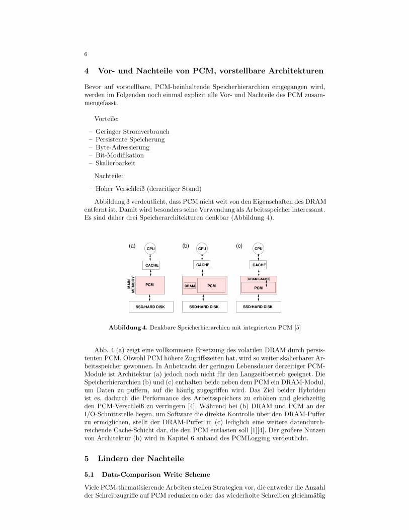
4 Vor- und Nachteile von PCM, vorstellbare Architekturen
Bevor auf vorstellbare, PCM-beinhaltende Speicherhierarchien eingegangen wird,werden im Folgenden noch einmal explizit alle Vor- und Nachteile des PCM zusam-mengefasst.
Vorteile:
– Geringer Stromverbrauch– Persistente Speicherung– Byte-Adressierung– Bit-Modifikation– Skalierbarkeit
Nachteile:
– Hoher Verschleiß (derzeitiger Stand)
Abbildung 3 verdeutlicht, dass PCM nicht weit von den Eigenschaften des DRAMentfernt ist. Damit wird besonders seine Verwendung als Arbeitsspeicher interessant.Es sind daher drei Speicherarchitekturen denkbar (Abbildung 4).
Table 1: Comparison of memory technologies.DRAM PCM NAND Flash HDD
Read energy 0.8 J/GB 1 J/GB 1.5 J/GB [28] 65 J/GBWrite energy 1.2 J/GB 6 J/GB 17.5 J/GB [28] 65 J/GBIdle power ∼100 mW/GB ∼1 mW/GB 1–10 mW/GB ∼10 W/TBEndurance ∞ 106 − 108 104 − 105 ∞Page size 64B 64B 4KB 512BPage read latency 20-50ns ∼ 50ns ∼ 25 µs ∼ 5 msPage write latency 20-50ns ∼ 1 µs ∼ 500 µs ∼ 5 msWrite bandwidth ∼GB/s per die 50-100 MB/s per die 5-40 MB/s per die ∼200MB/s per driveErase latency N/A N/A ∼ 2 ms N/ADensity 1× 2− 4× 4× N/ANote: The table contents are based mainly on [10, 15, 22].
"RESET" pulse
"SET" pulse
READ
Time
(Te
mp
era
ture
)C
urr
en
t
cryst
melt
T
T
Figure 1: Currents and timings (not to scale) forSET, RESET, and READ operations on a PCM cell.For phase change material Ge2Sb2Te5, Tmelt ≈ 610◦Cand Tcryst ≈ 350◦C.
the primary main memory, and the key challenge of over-coming its write limitations.
2.1 PCM TechnologyPhase change memory (PCM) is a byte-addressable non-
volatile memory that exploits large resistance contrast be-tween amorphous and crystalline states in so-called phasechange materials such as chalcogenide glass. The differencein resistance between the high-resistance amorphous stateand the low-resistance crystalline state is typically aboutfive orders of magnitude and can be used to infer logicalstates of binary data (high represents 0, low represents 1).Programming a PCM device involves application of elec-
tric current, leading to temperature changes that either SETor RESET the cell, as shown schematically in Figure 1. ToSET a PCM cell to its low-resistance state, an electricalpulse is applied to heat the cell above the crystalization tem-perature Tcryst (but below the melting temperature Tmelt) ofthe phase change material. The pulse is sustained for a suffi-ciently long period for the cell to transition to the crystallinestate. On the other hand, to RESET the cell to its high-resistance amorphous state, a much larger electrical currentis applied in order to increase the temperature above Tmelt.After the cell has melted, the pulse is abruptly cut off, caus-ing the melted material to quench into the amorphous state.To READ the current state of a cell, a small current thatdoes not perturb the cell state is applied to measure theresistance. At normal temperatures (< 120◦C ≪ Tcryst),PCM offers many years of data retention.
2.2 Using PCM in the Memory HierarchyTo see where PCM may fit in the memory hierarchy, we
need to know its properties. Table 1 compares PCM withDRAM (technology for today’s main memory), NAND flash
SSD/HARD DISK
ME
MO
RY
MA
IN
CACHE
PCM
CPU(a)
CACHE
SSD/HARD DISK
CPU
DRAM PCM
(b)
CACHE
SSD/HARD DISK
DRAM CACHE
CPU
PCM
(c)
Figure 2: Candidate main memory organizationswith PCM.
(technology for today’s solid state drives), and HDD (harddisk drives), showing the following points:
• Compared to DRAM, PCM’s read latency is close tothat of DRAM, while its write latency is about anorder of magnitude slower. PCM offers a density ad-vantage over DRAM. This means more memory capac-ity for the same chip area, or potentially lower priceper capacity. PCM is also more energy-efficient thanDRAM in idle mode.
• Compared to NAND Flash, PCM can be programmedin place regardless of the initial cell states (i.e., with-out Flash’s expensive “erase” operation). Therefore,its sequential and random accesses show similar (farsuperior) performance. Moreover, PCM has orders ofmagnitude higher write endurance than Flash.
Because of these attractive properties, PCM is being incor-porated in mobile handsets [24], and recent computer ar-chitecture and systems studies have argued that PCM is apromising candidate to be used in main memory in futuremainstream computer systems [9, 15, 22].
Figure 2 shows three alternative proposals in recent stud-ies for using PCM in the main memory system [9, 15, 22].Proposal (a) replaces DRAM with PCM to achieve largermain memory capacity. Even though PCM is slower thanDRAM, clever optimizations have been shown to reduce ap-plication execution time on PCM to within a factor of 1.2of that on DRAM [15]. Both proposals (b) and (c) includea small amount of DRAM in addition to PCM so that fre-quently accessed data can be kept in the DRAM buffer toimprove performance and reduce PCM wear. Their differ-ence is that proposal (b) gives software explicit control of theDRAM buffer [9], while proposal (c) manages the DRAM
22
Abbildung 4. Denkbare Speicherhierarchien mit integriertem PCM [5]
Abb. 4 (a) zeigt eine vollkommene Ersetzung des volatilen DRAM durch persis-tenten PCM. Obwohl PCM hohere Zugriffszeiten hat, wird so weiter skalierbarer Ar-beitsspeicher gewonnen. In Anbetracht der geringen Lebensdauer derzeitiger PCM-Module ist Architektur (a) jedoch noch nicht fur den Langzeitbetrieb geeignet. DieSpeicherhierarchien (b) und (c) enthalten beide neben dem PCM ein DRAM-Modul,um Daten zu puffern, auf die haufig zugegriffen wird. Das Ziel beider Hybridenist es, dadurch die Performance des Arbeitsspeichers zu erhohen und gleichzeitigden PCM-Verschleiß zu verringern [4]. Wahrend bei (b) DRAM und PCM an derI/O-Schnittstelle liegen, um Software die direkte Kontrolle uber den DRAM-Pufferzu ermoglichen, stellt der DRAM-Puffer in (c) lediglich eine weitere datendurch-reichende Cache-Schicht dar, die den PCM entlasten soll [1][4]. Der großere Nutzenvon Architektur (b) wird in Kapitel 6 anhand des PCMLogging verdeutlicht.
5 Lindern der Nachteile
5.1 Data-Comparison Write Scheme
Viele PCM-thematisierende Arbeiten stellen Strategien vor, die entweder die Anzahlder Schreibzugriffe auf PCM reduzieren oder das wiederholte Schreiben gleichmaßig

7
uber alle Zellen verteilen sollen [2]. Das Data-Comparison Write (DCW) Scheme hatersteres zum Ziel.Das konventionelle Schreibschema von PCM schreibt direkt in eine Zelle, unabhangigdavon, welche Daten sich zuvor in der Zelle befanden (Abbildung 5 (a)). Das DCWScheme soll genau dies verhindern, indem es die Notwendigkeit fur das Schreibenpruft. Bevor es zur Entscheidung kommt, ob in die PCM-Zelle geschrieben wird, wirdder aktuelle Wert der Zelle gelesen. Im Anschluss liegen der aktuelle Wert (ReadData) und der zu schreibende Wert (Write Data) vor. Diese werden miteinanderverglichen. Sind Read und Write Data gleich, so ist kein Schreiben notig, andern-falls wird nach dem konventionellen Schreibschema verfahren (Abbildung 5 (b)).Dadurch halbiert das DCW Scheme die Anzahl der tatsachlichen Schreibzugriffe aufeine PCM-Zelle, wenn alle Bit-Modifikationen gleichwahrscheinlich sind. Lediglichder Verbrauch einer Schreiboperation ist durch die vorher ausgefuhrte Leseopera-tion hoher. Dieser Mehraufwand ist jedoch durch die geringen Energiekosten einesREAD vernachlassigbar [3]. Eine ausfuhrliche Implementierung eines DCW-PCM-Moduls sowie die Testergebnisse eines ersten Prototyps finden sich in [3].
II. DATA-COMPARISON WRITE SCHEME
A. Concept of the DCW Scheme
(a) (b)
Figure 4. Flowchart of (a) Conventional write scheme (b) Proposed data-
comparison write scheme
TABLE I. POWER COMPARISON OF TWO WRITE SCHEMES
Conventional Scheme Proposed Scheme Cell Data
Transition Power Probability Power Probability
0 � 0 PSET 1/4 0 1/4
0 � 1 PRESET 1/4 PRESET 1/4
1 � 0 PSET 1/4 PSET 1/4
1 � 1 PRESET 1/4 0 1/4
Average
Power (PSET + PRESET)/2 (PSET + PRESET)/4
Fig. 4(a) shows the flowchart of the conventional write scheme. The conventional PRAM directly writes data on the selected PRAM cell independent of the previously stored data. If input data is ‘0’, the SET operation consumes the SET power (PSET). If input data is ‘1’, the RESET operation consumes the RESET power (PRESET). There are four cases for cell data transition as shown in Table 1. (0�0, 0�1, 1�0, 1�1) When the probabilities of four cases are 1/4, the average power of the conventional write scheme is (PSET + PRESET)/2.
Fig. 4(b) shows the flowchart of the proposed data comparison write (DCW) scheme. The DCW scheme performs the read operation before the write operation to know the previously stored data in the selected PRAM cell. If the input data and the previously stored data are the same, no write operation performs. If not, the write operation is the same as the conventional write scheme. When the probabilities of four cell data transitions are 1/4, the DCW scheme does not consume the write power for two cases (0�0, 1�1). Therefore, the average power of the DCW scheme is (PSET + PRESET)/4 which is a half of that of the conventional write scheme.
B. Circuit Implementation of the DCW-PRAM
Figure 5. Simplified block diagram of the DCW-PRAM
Figure 6. Simplified DCW circuit
Fig. 5 shows the simplified block diagram of the data comparison write PRAM (DCW-PRAM). Input address selects 8 cells with a selected word line and 8 selected bit lines. The pulse generator makes 3 timing pulse signals (READ_pulse, SET_pulse, RESET_pulse) with 3 external signals (Read, Write, Clock). The read circuit and write driver perform the read and write operations with 3 timing pulse signals and the write data.
Fig. 6 shows the simplified DCW circuit to write data. A PRAM cell is selected by an enabled word line (WL). A bit line (BL) is connected to the read and write circuits by a MUX. The read circuit senses the stored data from the GST resistance according to the stored data. The write circuit supplies SET and RESET current pulses to changes the GST resistance.
The PRAM uses two power supply voltages VCC and VDD. High voltage VCC is required to supply large SET and RESET currents into the GST cell. The MUX signals also use VCC to pass the write currents with high voltage. Low voltage VDD is used for most of circuits except for the write current related circuits.
Fig. 7 and 8 show waveforms of the conventional and proposed write operations, respectively. In the conventional write scheme, if the write data is ‘0’, a long SET current pulse is supplied into the selected PRAM cell. If the write data is ‘1’, a short SET current pulse is supplied. The conventional write scheme consumes the write power independent of the cell data transition. In the DCW scheme,
3015
Abbildung 5. Ablaufdiagramme des (a) konventionellen PCM-Schreibschemas und des(b) Data-Comparison Write Scheme [3]
5.2 Seitenersetzungsstrategien
Der Algorithmus least wear-unit difference (LWD) ist ein Seitenersetzungsal-gorithmus, der seine Ersetzungsentscheidung anhand einer kleinsten Wear-Unit-Differenz (WD) trifft. Wird eine angeforderte Seite p nicht im PCM gefunden(page miss), so vergleicht der LWD-Algorithmus p mit jeder Seite q im Speicherund verdrangt diejenige, die die kleinste Wear-Unit-Differenz zu p aufweist. Habenmehrere Seiten im Speicher die kleinste WD zu p, wird nach least recently used(LRU) verfahren [2].Die WD zweier Seiten wird ermittelt, indem jedes korrespondierende Paar vonPCM-Einheiten (wear units), z.B. durch gleichen Adressabstand innerhalb ihrerSeite, verglichen wird. Voneinander verschiedene Paare werden gezahlt. Kurz gesagt,beschreibt die WD somit die physikalische Ahnlichkeit der zwei betrachteten Seiten.LWD wahlt demnach die Seite als Verdrangungskandidaten, die der angeforderten
8
physikalisch am nachsten kommt, wodurch unter Verwendung des DCW Schemeweniger Bit-Modifikationen beim Schreiben benotigt werden. Bei einer Seitengroßevon P und einer Speicherkapazitat von B werden B * P viele Vergleiche zum Ermit-teln aller WD benotigt, woraus fur LWD eine Zeitkomplexitat von O(B ∗ P ) folgt[2].Was LWD jedoch nicht abdeckt, ist die Anzahl der bisher getatigten Uberschrei-bungen pro Seite (wear status). Er beeinflusst also nicht die Verteilung der Schreibzu-griffe, sodass es vorkommen kann, dass eine Seite ofter ersetzt wird als andere.Des Weiteren ist die Wahrscheinlichkeit fur zwei physikalisch identische Seiten mit1/(232) bei einer Wear-Unit-Große von 4 Byte sehr gering, wodurch LWD nicht denseitenubergreifenden Verschleiß reduziert [2].
Der Algorithmus least page wear (LPW) verfolgt einen anderen Ansatz alsLWD, indem er mit einem wear status (siehe 4.2.1) arbeitet, anstatt eine Wear-Unit-Differenz zu ermitteln. Wird eine Seite aus dem PCM verdrangt, so wird ihrVerschleißzahler (wear counter) um die Anzahl der zu andernden PCM-Zellen (wearunits) erhoht. LPW wahlt dann die Seite zur Verdrangung aus, die den geringstenVerschleißzahler besitzt. Der Verschleißzahler kann jedoch nur den wear status ap-proximieren, da er nicht die Verschleißverteilung innerhalb einer Seite reprasentiert.So kann es sein, dass eine Seite verdrangt wird, die wenige, oft modifizierte wearunits beinhaltet, trotzdem aber einen niedrigen Verschleißzahler aufweist. Da zurEntscheidung, welche Seite ersetzt werden soll, die mit dem niedrigsten Verschleiß-zahler im Speicher gefunden werden muss, besitzt LPW eine Zeitkomplexitat vonO(B). Hierbei ist B die Große des Speichers [2].
Der Algorithmus least frequently modified arbeitet nach einem ahnlichenPrinzip wie der klassische Algorithmus least frequently used (LFU). Um den wearstatus abzubilden, verwendet LFM pro Seite einen Modifikationszahler, der inkre-mentiert wird, wenn die Seite aus dem Speicher verdrangt wird. Der Modifika-tionszahler bleibt dafur nach der Verdrangung erhalten und wird nicht wie bei LRUzum Zeitpunkt der Auslagerung zuruckgesetzt. LFM wahlt demnach die Seite imSpeicher aus, die den niedrigsten Modifikationszahler besitzt und damit bisher amseltensten ersetzt, bzw. uberschrieben wurde. Um diese Seite zu ermitteln, muss derLFM-Algorithmus uber den gesamten Speicher der Große B gehen. Daraus folgt eineZeitkomplexitat von O(B) [2].
Nach dem Beispiel des LFM ist auch ein Algorithmus least recently modified(LRM), basierend auf dem klassischen Algorithmus least recently used (LRU),moglich, der die am langsten nicht modifizierte Seite verdrangt [2].
Testergebnisse zeigen, dass die vier vorgestellten Seitenersetzungsstrategien ef-fektiv die Lebensdauer eines PCM-Moduls erhohen konnen, obwohl sie nur die Ver-schleißverteilung auf Seitenebene beeinflussen, nicht aber die Verteilung innerhalbder Seiten. Fur detailliertere Informationen sei auf die Erstveroffentlichung der Al-gorithmen (siehe [2]) verwiesen.
5.3 Probabilistischer Record-Swapping-Algorithmus
Wahrend das in Kapitel 5.1 vorgestellte Data-Comparison Write (DCW) Schemedie Anzahl der Schreibzugriffe auf PCM reduziert, geht der probabilistische Record-Swapping-Algorithmus den Weg der Schreiblastverteilung uber das gesamte PCM-Modul. Damit ist sein Ziel die Vermeidung von hochfrequentiertem Schreiben in

9
immer dieselbe PCM-Stelle. Anwendung findet er beispielsweise in Datenbanksys-temen [1].
Soll ein Schreibzugriff auf PCM erfolgen, wird gepruft, ob der Speicherinhalt, aufden ein im DRAM gespeicherte Swap-Pointer zeigt, im Vergleich zum zu schreiben-den Datensatz kalt ist, also langer nicht mehr modifiziert wurde (cold record).Ist dies der Fall, wird der zu schreibende Datensatz an die Stelle des cold recordgeschrieben, nachdem dieser an eine freie Speicheradresse verschoben wurde (swap).Im Anschluss wird der Swap-Pointer auf die nachste PCM-Adresse gesetzt. AlsSwap-Kriterium verwendet der Algorithmus die aktuelle Transaktionsnummer (XID)Xc und die XID Xt des Datensatzes t, der vom Swap-Pointer referenziert wird. Istδ die systemweite Swap-Schwelle, so wird der zu schreibende Datensatz und t ver-tauscht, wenn Xc −Xt ≥ δ gilt. Da die XID eine monoton steigende Zahl ist, stelltdie Differenz ein gutes Maß fur die Zeit der letzten Modifikation von t dar. Furden Fall Xc−Xt < δ ist eine fest gewahlte Swap-Schwelle nicht optimal, da sie po-tentiell zu einer langeren Wartezeit fuhren kann, bis ein Swap-Kandidat gefundenwird. Ist δ zu groß gewahlt, kommt es zu geringerer Schreibverteilung bei ebenfallsgeringem Schreibmehraufwand durch den Algorithmus, wohingegen ein zu kleines δzu hohen Schreibmehraufwand mit sich bringt. Daher wird eine Wahrscheinlichkeitvon Xc−Xt
δ vorgeschlagen, die Datensatze trotzdem zu vertauschen [1].Der probabilistische Record-Swapping-Algorithmus vermeidet demnach, dass eincold record eine Speicheradresse uber eine langere Zeit fur sich beansprucht, in-dem er die Speicherplatze von cold records durch eintreffende, potentiell heißeDatensatze (hot records) ersetzt. Potentielle Hotspots erhalten so kalte Adressen.Trotz des Schreibmehraufwandes auf dem PCM, zeigen erste Testergebnisse eineLebensdauerverlangerung um das 5-fache bei einer um 34% erhohten Anzahl anSchreibzugriffen [1].
6 PCMLogging
In diesem Kapitel wird ein Logging-Schema vorgestellt, welches auf einer PCM-Architektur arbeitet, wie sie in Abbildung 4 (b) zu sehen ist. Die Grundidee desPCMLogging besteht darin, den Transaktionslog und die modifizierten Daten zukombinieren und im PCM zu speichern, um so die Persistenz vom PCM geschickt zunutzen. In Kapitel 6.2 wird PCMLogging auf Seitenebene vorgestellt, um das Vorge-hen leichter verdeutlichen zu konnen. Um die Transaktionsverarbeitung von PCM-Logging weiter zu optimieren, wird in Kapitel 6.3 auf eine Erweiterung auf Satzebeneeingegangen. Jegliches Wissen uber PCMLogging in diesem Kapitel wurde aus [1]generiert.
6.1 Datenstrukturen und Grundlagen
Folgende Datenstrukturen werden fur das PCMLogging im DRAM, bzw. PCMbenotigt:
– Mapping Table: Die Mapping-Tabelle wird im DRAM gehalten und dient derAbbildung logischer Seiten-IDs zu physischen PCM-Adressen. Sie liegt nicht imPCM, da ihre Eintrage haufig modifiziert werden und PCM langsamer ist alsDRAM.
– Inverse Mapping: Das inverse Mapping ist Teil der Metadaten einer Seite (kurzPID) und wird fur die Rekonstruktion der initialen Mapping Table beim Sys-temstart benotigt.
– FreeSlotBitmap: Die FreeSlotBitmap speichert, welche PCM-Speicherplatze nochnicht belegt sind. Sie ist im PCM abgelegt.

10
– ActiveTxList: Mithilfe dieser Liste werden sich alle Transaktionen gemerkt, dienoch laufen und deren modifizierten Seiten (dirty pages) sich im PCM befinden.Sie wird fur das Transaktions-Recovery benotigt und ist ebenfalls im PCMgespeichert.
– Transaction Table (TT): Die Transaktionstabelle beinhaltet alle noch laufendenTransaktionen. Fur jede Transaktion wird dabei eine Liste aller modifiziertenSeiten gespeichert, die sich im DRAM oder PCM befinden. Bei einem Commitoder Abort kann so schnell auf die durch die Transaktion geanderten Seitenzugegriffen werden.
– Dirty Page Table (DPT): Die Dirty Page Table halt Referenzen auf zuvor miteinem Commit abgeschlossene Versionen jeder Seite, die durch eine laufendeTransaktion modifiziert wurde.
TABLE I
COMPARISON OFSTORAGE TECHNOLOGIES[4]
Parameter DRAM Flash HDD PCMDensity 1X 4X N/A 2-4X
Read latency(granularity)
20-50ns ∼25µs ∼5ms ∼50ns(64B) (4KB) (512B) (64B)
Write latency(granularity)
20-50ns ∼500µs ∼5ms ∼1µs(64B) (4KB) (512B) (64B)
Endurance(write cycles) N/A 104-105 ∞ 106-108
• Fine-grained access:Compared to other non-volatilememory technologies such as flash memory, erase-before-write and page-based access do not restrain PCM. It isbyte addressable (or word addressable) and bit alterable,which enable PCM to support small in-place updates.
• Asymmetric read/write latency:As shown in Table I, thewrite speed of PCM is about 20 times slower than itsread speed. This is similar to flash memory that has suchan asymmetry as well.
• Endurance limitation:Similar to flash memory, PCMendures a limited number of writes, about106 to 108
writes for each cell, which is however much higher thanthat of flash memory.
• Low idle energy consumption:While PCM uses for dataaccess similar energy as DRAM (i.e., 1-6 J/GB), itconsumes much lower idle energy compared to DRAM(i.e., 1 v.s. 100mW/GB).
This paper focuses on improving transaction logging andrecovery performance by PCM integration. For this purpose,we mainly exploit PCM’s low access latency and fine-grainedaccess granularity and address its endurance limitation.
B. PCM in the Memory Hierarchy
So far, two representative architectures for the use of PCMin a memory hierarchy are proposed [6], [22]: 1) PCM co-existing with DRAM to serve as main memory (as shownin Figure 1(a)); 2) main memory only composed of PCMchips thereby fully replacing DRAM. Considering the hard-ware features of PCM, the co-existence architecture might bemore practical. The first reason is that PCM has endurancelimitation, which prevents a complete replacement of DRAM.Secondly, write latency of PCM is still 20-50 times largerthan that of DRAM. Thirdly, PCM capacity is expected tostill remain relatively small in the near future, in comparisonwith DRAM. Thus in this study, we focus on the memoryarchitecture using PCM as an auxiliary memory, being astaging area between DRAM and external disks.
III. PCML OGGING
We consider the memory architecture as shown in Fig-ure 1(a). Without largely modifying the buffer manager re-siding in DRAM memory, we present a new logging scheme,called PCMLogging, where the cached updates and transactionlog records are combined and kept in PCM. The wear-levelingand data destaging issues of PCMLogging will be discussedin Sections IV and V.
Fig. 2. Page format and Mapping Table
A. Overview
The basic idea of PCMLogging is to integrate the transac-tion log into the updates cached in PCM, by exploiting thepersistence property of PCM storage. For ease of exposition,we assume in this section that PCM caching granularity is apage and concurrency control is also at a page level. That is,apage can be updated by at most one transaction at a time. Tofurther improve transaction processing performance, we willextend the design to record-level caching and record-basedconcurrency control in Section III-C.
Overview of the PCMLogging scheme: To support datacaching in PCM, we maintain the following data structuresin main memory (DRAM) / PCM (see Figure 2):
• Mapping Table.This table maps logical page IDs tophysical PCM addresses. It is maintained in DRAMrather than in PCM, because the mapping entries arefrequently updated and the write speed of PCM is 20-50 times slower than that of DRAM.
• Inverse Mapping.The inverse mapping is embedded ineach PCM page as metadata (i.e., PID). It is used toconstruct the initial Mapping Table at boot time.
• FreeSlotBitmap.This bitmap is used to keep track of thefree page slots in PCM. Note for PCMLogging, onlythe dirty pages evicted from main memory are cachedin PCM to minimize disk write I/Os.
Inspired by shadow paging [9], we adopt an out-of-placeupdate scheme in PCM. When a transaction is to commit,all its dirty pages are flushed to PCM to ensure durability.Also, when a dirty page is evicted from main memory, itwill be cached in PCM. For each dirty page, if there alreadyexists a previously committed version in PCM, the committedversion will not be overwritten. Instead, the previous versionis retained, while the dirty page as new version is written toa free PCM slot. After that, the logical page address in theMapping Table is adjusted to the new version. The need ofretaining the previously committed version is to support undooperations in case of transaction rollback or system crash.
To support transaction recovery, an ActiveTxList is main-tained in PCM to record the in-progress transactions that havedirty pages cached in PCM. Each cached page records theXID of the last transaction that caused the page to be dirty.Before the first dirty page of a transaction is written to PCM,its corresponding XID should be recorded in the ActiveTxList
Abbildung 6. Seitenformat und Mapping Table [1]
Anzumerken ist, dass nur dirty pages im PCM gespeichert werden, die aus demDRAM verdrangt wurden oder deren Anderungstransaktion mit einem Commitabschließt, um Dauerhaftigkeit der Daten zu gewahrleisten. Des Weiteren arbeitetPCMLogging nach dem Shadow-Paging-Verfahren, indem eine Seitenmodifikationnicht auf der vorherigen Version einer Seite, sondern auf einer Kopie stattfindet.Fur die Versionenubersicht ist die Dirty Page Table zustandig, die im Falle einesSystemabsturzes oder Transaktions-Rollback eine Undo-Operation ermoglicht. DieXID der letzten andernden Transaktion sowie eine Versionsnummer sind ebenfallsTeil der Metadaten einer Seite [1].Um Atomaritat zu garantieren, wird eine Seite einer Transaktion erst in den PCMgeschrieben, wenn die korrespondierende XID in die ActiveTxList aufgenommenwurde. Die XID wird erst aus der ActiveTxList entfernt, wenn die zugehorigeTransaktion mit einem Commit abschließt und alle dirty pages aus dem DRAMin den PCM verdrangt wurden. Wird also wahrend des Recovery-Prozesses eineTransaktion in der ActiveTxList gefunden, so war sie zum Zeitpunkt des Sys-temabsturzes noch nicht abgeschlossen. Beispielsweise wurden die Anderungen vonTransaktion 1 in Abbildung 6 verworfen werden, wenn wir annehmen, dass nurSeiten zum externen Speicher zuruckgeschrieben werden, die von einer mit Commitabgeschlossenen Transaktion modifiziert wurden. Die Speicherplatze M5 und M7bleiben unverandert, da Transaktion 2 rechtzeitig mit einem Commit abgeschlossenwurde. Die FreeSlotBitmap wird angepasst zu 00001010. Gegebenenfalls werden dieSeiten in M5 und M7 auf ein externes Speichermedium zuruckge-schrieben [1].
11
6.2 Vorgehen auf Seitenebene
In diesem Kapitel werden eine PCM-Granularitat von genau einer Seite und einNebenlaufigkeitsverhalten auf Seitenebene vorausgesetzt. Durch Seitensperren kannzu jeder Zeit nur hochstens eine Transaktion eine Seite modifizieren. NotwendigeOperationen werden von PCMLogging wie folgt umgesetzt:
– Verdrangung modifizierter Seiten zum PCM (DRAM-Puffer mit Steal-Politik). Falls der DRAM voll wird oder eine Transaktion mit einem Commitabschließt, mussen modifizierte Seiten (dirty pages) verdrangt werden. Bevoreine ausgewahlte Seite M in den PCM verschoben wird, muss die zugehorigeTransaktions-XID in die ActiveTxList im PCM aufgenommen werden, falls sienicht schon vorhanden ist. Besitzt M Vorgangerversionen, deren Anderungstrans-aktionen mit einem Commit abgeschlossen haben, erstellen wir eine Kopie M’von M mit erhohter Versionsnummer und speichern M’ an einen anderen Platz.M wird der Dirty Page Table mit Verweis auf M’ hinzugefugt und der Eintrag derandernden Transaktion in der Transaction Table wird aktualisiert. Ein Beispielist in Abbildung 7 (a) und (b) illustriert: T1 ist noch in Arbeit, wahrend T2 bere-its mit einem Commit abgeschlossen hat. T3 modifiziert die Seite P5, befindlichim DRAM (siehe Abb. 7 (a)). Anschließend wird P5 zu PCM-Speicherplatz M8verdrangt. T3 wird der ActiveTxList hinzugefugt, P5 verweist in der MappingTable ab sofort auf M8, in der Transaction Table zeigt T3 auf M8 und M7 wirdals vorherige Version von M8 in der Dirty Page Table aufgenommen (siehe Abb.7 (b)).
– Commit. Mochte eine Transaktion mit einem Commit abschließen, wird mithilfeder Transaction Table jede noch im DRAM befindliche dirty page in den PCMgeschrieben. Anschließend wird der Commit gultig gemacht, indem die zurTransaktion korrespondierende XID aus der ActiveTxList geloscht wird. Esfolgt eine Anpassung der FreeSlotBitmap anhand der Dirty Page Table. Allevorherigen Versionen der verdrangten Seiten werden verworfen, indem derenFreeSlotBitmap-Eintrage auf 0 gesetzt werden. Abschließend werden die zurTransaktion zugehorigen Eintrage in der Dirty Page Table und der TransactionTable geloscht. Abbildung 7 (c) veranschaulicht das PCM-Logging-Verhaltenbei einem Commit: T3 mochte mit einem Commit abschließen. Da alle von T3modifizierten Seiten bereits im PCM liegen, wird T3 aus der ActiveTxList ent-fernt und die vorherige Version von P5 in M7 sowie deren Eintrag in der DirtyPage Table werden verworfen (siehe FreeSlotBitmap und DPT). Zum Schlusswird T3 aus der Transaction Table herausgestrichen.
– Abort. Wird eine Transaktion abgebrochen, werden alle zugehorigen dirtypages aus dem PCM verworfen (durch eine Anderung der FreeSlotBitmap). Fallseine dieser Seiten in der Dirty Page Table vorkommt, wird die vorherige, zuletztcommittete Version wiederhergestellt, indem die Mapping Table angepasst wird.Abschließend werden die Transaktions-XID aus der ActiveTxList und zugehorigeEintrage aus der Transaction und der Dirty Page Table entfernt. Abbildung 7(d) zeigt einen Abbruch von T3. Demnach wird die aktuelle Version in M8verworfen, der Verweis auf die letzte gultige Version in M7 in der MappingTable wiederhergestellt und es werden korrespondierende Eintrage in der Ac-tiveTxList, der Dirty Page Table und der Transaction Table entfernt.
– Recovery. Nach einem Systemabsturz werden alle Seiten im PCM gepruft, obsie die zuletzt gultige Version sind. Dabei werden alle Speicherplatze uberpruft,die in der FreeSlotBitmap den Wert 1 haben. Jede Seite, die von einer vor demAbsturz noch laufenden Transaktion (siehe ActiveTxList) modifiziert wurde,wird verworfen, indem an der korrespondierenden Stelle in der FreeSlotBitmapeine 0 geschrieben wird. Aus den ubrig bleibenden wird die Mapping Tablerekonstruiert. Selbst wenn der Fall eintritt, dass der Absturz in Abbildung 7 (c)

12
erfolgt, nachdem T3 von der ActiveTxList entfernt und M7 noch nicht verworfenwurde, kann mithilfe der Versionsnummern der Seiten in M7 und M8 die letztecommittete Seitenmodifikation identifiziert werden. Erwahnenswert ist, dass dergesamte Recovery-Vorgang keinen Zugriff auf einen externen Speicher benotigt[1].
to guarantee atomicity. The XID is not removed until thetransaction is to commit and all its dirty pages are flushedto PCM. Thus, during recovery, if the XID of a transaction isfound in the ActiveTxList, it implies that the transaction wasnot yet committed before the crash; otherwise, the transactionwas already committed. Consequently, each PCM page canbe recovered according to the status of the correspondingtransaction. For example, if PCM appears as shown in the rightpart of Figure 2, we can infer thatT1 is not yet committed,whereasT2 is committed. Thus, the pages updated byT1 (i.e.,those stored inM1-M3) are discarded,2 whereas the pagesupdated byT2 (i.e., those stored inM5 andM7) need to berestored. Accordingly, the FreeSlotBitmap will be updatedto“00001010.” We note that, to avoid hot-spots in PCM, wear-leveling techniques should be adopted to evenly distributewrites across the PCM space, which will be discussed in moredetail in Section IV.
As a brief summary, PCMLogging eliminates the explicittransaction log by integrating it into the dirty pages cachedin PCM. This integrated design has several advantages. First,the data redundancy between the log and cached updates isminimized. Second, it avoids the challenging space manage-ment issue, which is a must if they are separated. Third,recovery can be done without checkpoints, because we donot maintain an explicit log. In addition, the recovery processbecomes extraordinarily simple and efficient. In the following,we describe the PCMLogging scheme in detail.
B. PCMLogging Operations
Durability is achieved by forcing the affected dirty pages toPCM when a transaction is to commit. On the other hand, asteal buffer policy allows a dirty page to be flushed to PCMbefore the transaction commits. To ensure atomicity, undooperations will be needed if the transaction is finally aborted.To efficiently support such undo operations, we maintain twoadditional data structures in main memory:
• Transaction Table (TT).This table records all in-progresstransactions. For each of them, it keeps track of allits dirty pages stored in main memory and PCM. Thepurpose is to quickly identify relevant pages when thetransaction is to commit or abort.
• Dirty Page Table (DPT).This table keeps track of thepreviously committed version of each PCM page “over-written” by an in-progress transaction. Recall that we em-ploy out-of-place updates in PCM. This is necessary forrestoring the previously committed version in the eventof a rollback. A dirty page entry will be removed fromthe table, once the in-progress transaction is committedor aborted.
PCMLogging needs to handle the following key events:Flushing Dirty Pages to PCM. When main memory
becomes full or a transaction is to commit, some dirty pagesmay need to be flushed to PCM. For each dirty page, we firstcheck the Transaction Table. If it is the first dirty page of thetransaction to be flushed to PCM, we add the related XIDto the ActiveTxList in PCM before flushing. If there exists a
2They have not left the PCM, because our destaging algorithm (Section V)only flushes committed pages to external storage.
Fig. 3. An example of PCMLogging (MT: Mapping Table; TT: TransactionTable; DPT: Dirty Page Table)
previously committed versionM in PCM, we do not overwriteit in place. To support undo, we create instead an out-of-placecopyM ′ with a larger version number. Then,M is added tothe Dirty Page Table and the page is mapped toM ′ in theMapping Table. Finally, the Transaction Table is updated.
Commit. Upon receiving a commit request, all dirty pagesof the transaction being still buffered in main memory areforced to PCM, by consulting the Transaction Table. Afterthat, we remove its XID from the ActiveTxList to indicate thetransaction is committed. Next, if any of its pages is containedin the Dirty Page Table, the previous versions are discardedby resetting their corresponding bits in the FreeSlotBitmap.Finally, we clear the relevant entries in the Transaction Tableand Dirty Page Table.
Abort. When a transaction is aborted, all its dirty pagesare discarded from PCM, by consulting the Transaction Table.If any of its pages is contained in the Dirty Page Table, thecurrent version should be invalidated and the mapping shouldbe re-mapped (restored) to the previous version in the MappingTable. Finally, we clear its XID in the ActiveTxList and therelevant entries in the Transaction Table and Dirty Page Table.
An Example: Consider the example shown in Figure 3,where T1 is in progress and T2 is committed. Suppose now anew transaction T3 updates page P5. Before this dirty pageis flushed, T3 points to page P5 kept in main memory (seeFigure 3(a)). When it is flushed to PCM slot M8, T3 is addedto the ActiveTxList in PCM (see Figure 3(b)). After that, P5 ismapped to M8, T3 points to M8, and the previous version M7 iskept in the Dirty Page Table. Finally, if T3 is to commit, it isre-moved from the ActiveTxList; the previous version is discarded(the corresponding bit becomes 0 in the FreeSlotBitmap); andthe corresponding entries are removed from the TransactionTable and Dirty Page Table (see Figure 3(c)). Otherwise, ifT3 is finally aborted, the current version is discarded (thecorresponding bit becomes 0 in the FreeSlotBitmap) and theprevious version is restored in the Mapping Table; and thecorresponding entries are also removed from the ActiveTxList,Transaction Table, and Dirty Page Table (see Figure 3(d)).
Recovery.A recovery process is invoked when the systemrestarts after a failure. It identifies the last committed version
Abbildung 7. Ein Beispiel zur Verdeutlichung des PCMLogging (MT: Mapping Table,TT: Transaction Table, DPT: Dirty Page Table) [1]
6.3 Vorgehen auf Satzebene
In diesem Kapitel wird eine PCMLogging-Erweiterung vorgestellt, die nicht mehrauf Seiten-, sondern auf Satzebene arbeitet. Dazu werden anstelle von modifiziertenSeiten nun modifizierte Satze im PCM zwischengespeichert.Ein PCMLogging-Schema auf Satzebene hat mehrere Vorteile. Zum einen wirdweniger Speicherplatz auf dem PCM benotigt, da Satze nur kleine Teile einer Seitesind. Zum anderen reduziert es die Anzahl der Schreibzugriffe auf den PCM, was eineLebensdauerverlangerung des Moduls und weniger Verdrangungen zur Folge hat.Des Weiteren werden satzbasierte Nebenlaufigkeitsverfahren unterstutzt, welche beimodernen Datenbanksystemen ein hohes Maß an Nebenlaufigkeit gewahrleisten [1].Die Datenstrukturen von PCMLogging werden wie folgt erweitert bzw. angepasst:
– Die Speicherplatze des PCM werden an die Satzgroße angepasst. Das Satzfor-mat gleicht dem Seitenformat bis auf die Nutzdaten, die nun Satze sind undeinem zusatzlichen Metadatenfeld namens SNO. Die Slot-Nummer (SNO) unddie Seiten-ID bilden die Satz-ID (RID). Zur Verwaltung freien Speichers kannebenfalls eine FreeSlotBitmap verwendet werden.
– In der Mapping Table werden immer noch modifizierte Seiten verwaltet, jedochspeichert jede Seite alle Abbildungen auf modifizierte Satze (dirty records), z.B.mithilfe eines binaren Baums basierend auf der RID.
– Mit der Dirty Page Table wird ahnlich verfahren, sodass jede Seite in der TabelleVerweise zu Vorgangerversionen der jeweiligen Satze enthalt.

13
– Zusatzlich wird eine Liste fur jede Seite angelegt, die speichert, welche zugehori-gen dirty records sich im DRAM befinden. Wenn eine Transaktion mit einemCommit abschließen will oder eine Seite aus dem DRAM verdrangt werden muss,so konnen zugehorige Satze schnell identifiziert und in den PCM geschriebenwerden.
– Die Transaction Table unterhalt eine Liste aller laufenden Transaktionen undderen dirty records.
– Durch die Mapping Table kann ein schneller Zugriff auf einen Satz im PCMerfolgen, wenn er vorliegt. Wird eine ganze Seite angefordert, so wird diese vomexternen Speicher geladen und mit den zuletzt gultigen, seitenrelevanten Satzen,die im PCM zwischengespeichert sind, zusammengefuhrt. Da die Ladevorgangeparallel stattfinden, ist die Zugriffslatenz des PCM gegenuber der des externenSpeichers vernachlassigbar.
– Damit der PCM nicht volllauft, sollten wahrend des Betriebes oder idealer-weise in Systemleerlaufzeiten Satze mit Commit abgeschlossener Transaktionenauf das externe Speichermedium zuruckgeschrieben werden. Hierzu wird die zuden Satzen korrespondierende Seite vom externen Speicher geladen, mit den imPCM befindlichen Satzen zusammengefuhrt und wieder zuruckgeschrieben.
Die Arbeitsweise der vier Operationen des PCMLogging ist auf Satzebene wie folgtrealisiert:
– Verdrangung modifizierter Satze zum PCM. Satz t, der zuletzt durchTransaktion T modifiziert wurde, soll verdrangt werden. Ist t der erste dirtyrecord, der im PCM zwischengespeichert werden soll (siehe ActiveTxList), sowird T der ActiveTxList hinzugefugt. Anschließend wird t in einen freien Spei-cherplatz vom PCM geschrieben. Existiert eine fruhere Version von t im PCM,deren Anderungstransaktion mit einem Commit abgeschlossen hat, so verweistt in der Dirty Page Table ab sofort auf diese. Ansonsten, falls bereits eine Kopievon t vorliegt, wird diese verworfen, indem das korrespondierenden Bits in derFreeSlotBitmap auf 0 gesetzt wird. Abschließend verweist T in der TransactionTable zusatzlich auf t und der Adresseintrag von t in der Mapping Table wirdaktualisiert.
– Commit. Transaktion T will mit einem Commit abschließen. Zu Beginn wirdjeder von T modifizierten Satz aus dem DRAM (zu finden in der TransactionTable) verdrangt. Anschließend wird T von der ActiveTxList im PCM entferntund vorherige Versionen der zu T gehorigen dirty records (zu finden uber dieDirty Page Table) werden verworfen, indem deren korrespondieren Bits in derFreeSlotBitmap auf 0 gesetzt werden. Abschließend werden die Eintrage von Tin der Transaction Table und der Dirty Page Table geloscht.
– Abort. Transaktion T wird abgebrochen, erhalt also ein Abort. Mithilfe derTransaction Table werden alle dirty records sowohl im DRAM, als auch im PCMgefunden und durch Anderungen an der FreeSlotBitmap verworfen. Wenn Tnoch in der ActiveTxList zu finden ist, werden mithilfe der Dirty Page Table diezuletzt gultigen Versionen der dirty records von T wiederhergestellt. Außerdemwird die Mapping Table auf die vorherigen Versionen aktualisiert und T wirdvon der ActiveTxList entfernt. Abschließend werden alle Eintrage, die von Tsind, in der Transaction Table und DirtyPageTable geloscht.
– Recovery. Alle Satze, die nach der FreeSlotBitmap valide sind (an der korre-spondierenden Stelle ist eine 1 gespeichert), werden uberpruft, ob deren XID inder ActiveTxList steht oder bereits eine hohere Version vorliegt. Erfullt ein Satzt diese Bedingung, wird sie durch Anderung der FreeSlotBitmap verworfen. An-sonsten wird fur t ein Eintrag in der Mapping Table im DRAM angelegt. Letz-terer Fall kann beispielsweise dann auftreten, wenn ein Satz aus dem DRAM

14
zum PCM verdrangt wird und es vor der Aktualisierung der Mapping Table zueinem Systemabsturz kommt.
6.4 Performance-Aspekte
In [1] wird die Verwendung PCMLogging umfangreich fur Datenbanken simuliertund analysiert. In diesem Kapitel wird lediglich das Gesamtergebnis verschiedenerTests vorgestellt. Fur ausfuhrlichere Informationen, beispielweise zu der verwende-ten Testumgebung, sei auf [1] verwiesen.Verglichen wurden drei Logging-Schemata:
– SCMLogging: Das PCM-Modul dient ausschließlich der Speicherung des Transak-tionslogs.
– WAL (nach Write-ahead logging): Einteilung des PCM in zwei Zonen. In der er-sten Zone werden modifizierte Seiten zwischengespeichert, in der zweiten Trans-aktionslogeintrage. Wird eine Seite aus dem DRAM verdrangt, wird sie in er-ster Zone gespeichert. Lauft diese Zone voll, wird ein klassischer Ersetzungsal-gorithmus wie LRU angewendet, um erneut Speicherplatz zu schaffen. Endeteine Transaktion mit einem Commit, werden alle Logeintrage im DRAM in dieLogzone des PCM heruntergeschrieben. Ist diese Zone voll, kann entweder einCheckpoint-Prozess oder ein Zuruckschreiben auf den externen Speicher erfol-gen. WAL verwendet Update-in-Place.
– PCMLogging auf Satzebene (siehe Kapitel 6.3).
Festzuhalten ist, dass WAL in allen Testfallen besser als SCMLogging abschneidet.Das hat zum einen den Grund, dass WAL Daten im PCM zwischenspeichert, was dieI/O-Kosten senkt, und zum anderen, dass das SCMLogging jeden neuen Logeintragin den PCM schreibt, was hohere Latenzen verursacht, als das Schreiben in denDRAM, wie es WAL macht [1].
TABLE II
DEFAULT PARAMETER SETTINGS
Parameter Default SettingHDD read/write latency 8.05ms/8.20msSSD read/write/erasure latency 0.11ms/0.32ms/1.5msSD card read/write latency 1.47ms/200.1msPCM write latency 1µsLogical page size 8KBPCM unit size 128BTPC-C database size 2.4GBTPC-C client number/warehouse number 50/20Main memory (DRAM) size 128MBPCM size 128MB
We compared three logging schemes: our record-level PCM-Logging scheme (denoted as PCMLogging), the WAL designof using PCM for both data caching and transaction logging(detailed in the Introduction section, denoted as WAL), andarecent proposal of using storage-class memory such as PCMfor logging only (denoted as SCMLogging) [8]. Note thatthe page-level PCMLogging scheme was not evaluated asit does not support record-level concurrency control. For afair comparison using PCMLogging, the main memory areaincluded the space needed for holding the data structuresof PCM management (such as Mapping Table and DirtyPage Table). For the destaging process of PCMLogging, weassumed the rate relationship functiong(k) = 1 for simplicity(f(k)’s were measured during warm up). For WAL, as it isdifficult to determine the optimal space allocation betweenthecache and log zones, we used for simplicity the whole PCMspace for data caching and reserved an additional page forarchiving log records. For SCMLogging, the log records werecreated and maintained in PCM directly. In general, the WALand SCMLogging schemes represent two typical usages ofPCM, i.e., maximizing its caching or logging capabilities. Inboth of these schemes, the log records archived in PCM canbe flushed out to external disks asynchronously.
We conducted the simulation experiments on a desktopcomputer running Windows 7 Enterprise with an Intel i7-2600 3.4GHz CPU. As we simulated a database of 2.4GB,the default sizes of DRAM and PCM were both set at128MB (i.e., total 10% of the database size). For all schemes,the results were collected after a fixed warmup period (i.e.,after PCMLogging starts the first destaging process). TableIIsummarizes the settings of our simulation experiments.
B. Overall Performance Comparison
In this section, we report the overall comparison of PCM-Logging with WAL and SCMLogging. We plot the transactionthroughput and response time of the three schemes in Fig-ures 6(a) and 6(b), respectively, by varying the size of PCMfrom 32MB to 160MB. We make the following observationsfrom the results. First, WAL has a better performance thanSCMLogging in all cases tested. The reason can be explainedas follows: i) applying WAL, PCM is not only used for loggingbut also for data caching, which makes its I/O cost less thanthat of SCMLogging (see Figure 7(a)); ii) using SCMLogging,each transactional update incurs a PCM write to create anew log record, which causes a larger latency than a writein DRAM needed in case of WAL. Second, PCMLogging
(a) Transaction throughput (b) Transaction response time
Fig. 6. Overall performance results
has the best performance among all the three schemes. InFigure 6(a), the throughput improvement of PCMLoggingover WAL increases from 19.2% to 78.3%, as the PCM sizegrows. A similar trend is observed for the response time inFigure 6(b). This confirms our argument that PCMLoggingcan better exploit the PCM hardware features for superiorperformance improvements. Next, we reveal more details ofthe PCMLogging performance from various perspectives.
I/O Breakdown: We decompose the total I/O number intoreads and writes and plot the I/O breakdown in Figure 7(a).Obviously, the total I/O number of SCMLogging remains thesame under different PCM sizes, because it writes only logrecords to PCM. In contrast, due to data caching in PCM, thetotal I/Os of WAL and PCMLogging decrease as the size ofPCM grows. In particular, compared with WAL, PCMLoggingsaves 21.5%∼46.6% of total I/Os under different PCM sizes.The saving is mainly due to reduced write I/Os (the upper partof each bar). For example, when the PCM size is 128MB,the number of write I/Os of PCMLogging is only 12.7%of that of WAL. Note, the write I/Os for PCMLogging arerecord destaging operations, whereas they are PCM pagereplacements for WAL.
To gain more insights, we further measure the averagenumber of dirty records per page for each write I/O operationand plot the results in Figure 7(b). This number indicates theefficiency of flushing dirty information from DRAM/PCM to
(a) I/O breakdown
(b) Dirty records per page (c) Read I/Os and PCM hitsFig. 7. I/O breakdown comparison
(a) Transaktionsdurchsatz
TABLE II
DEFAULT PARAMETER SETTINGS
Parameter Default SettingHDD read/write latency 8.05ms/8.20msSSD read/write/erasure latency 0.11ms/0.32ms/1.5msSD card read/write latency 1.47ms/200.1msPCM write latency 1µsLogical page size 8KBPCM unit size 128BTPC-C database size 2.4GBTPC-C client number/warehouse number 50/20Main memory (DRAM) size 128MBPCM size 128MB
We compared three logging schemes: our record-level PCM-Logging scheme (denoted as PCMLogging), the WAL designof using PCM for both data caching and transaction logging(detailed in the Introduction section, denoted as WAL), andarecent proposal of using storage-class memory such as PCMfor logging only (denoted as SCMLogging) [8]. Note thatthe page-level PCMLogging scheme was not evaluated asit does not support record-level concurrency control. For afair comparison using PCMLogging, the main memory areaincluded the space needed for holding the data structuresof PCM management (such as Mapping Table and DirtyPage Table). For the destaging process of PCMLogging, weassumed the rate relationship functiong(k) = 1 for simplicity(f(k)’s were measured during warm up). For WAL, as it isdifficult to determine the optimal space allocation betweenthecache and log zones, we used for simplicity the whole PCMspace for data caching and reserved an additional page forarchiving log records. For SCMLogging, the log records werecreated and maintained in PCM directly. In general, the WALand SCMLogging schemes represent two typical usages ofPCM, i.e., maximizing its caching or logging capabilities. Inboth of these schemes, the log records archived in PCM canbe flushed out to external disks asynchronously.
We conducted the simulation experiments on a desktopcomputer running Windows 7 Enterprise with an Intel i7-2600 3.4GHz CPU. As we simulated a database of 2.4GB,the default sizes of DRAM and PCM were both set at128MB (i.e., total 10% of the database size). For all schemes,the results were collected after a fixed warmup period (i.e.,after PCMLogging starts the first destaging process). TableIIsummarizes the settings of our simulation experiments.
B. Overall Performance Comparison
In this section, we report the overall comparison of PCM-Logging with WAL and SCMLogging. We plot the transactionthroughput and response time of the three schemes in Fig-ures 6(a) and 6(b), respectively, by varying the size of PCMfrom 32MB to 160MB. We make the following observationsfrom the results. First, WAL has a better performance thanSCMLogging in all cases tested. The reason can be explainedas follows: i) applying WAL, PCM is not only used for loggingbut also for data caching, which makes its I/O cost less thanthat of SCMLogging (see Figure 7(a)); ii) using SCMLogging,each transactional update incurs a PCM write to create anew log record, which causes a larger latency than a writein DRAM needed in case of WAL. Second, PCMLogging
(a) Transaction throughput (b) Transaction response time
Fig. 6. Overall performance results
has the best performance among all the three schemes. InFigure 6(a), the throughput improvement of PCMLoggingover WAL increases from 19.2% to 78.3%, as the PCM sizegrows. A similar trend is observed for the response time inFigure 6(b). This confirms our argument that PCMLoggingcan better exploit the PCM hardware features for superiorperformance improvements. Next, we reveal more details ofthe PCMLogging performance from various perspectives.
I/O Breakdown: We decompose the total I/O number intoreads and writes and plot the I/O breakdown in Figure 7(a).Obviously, the total I/O number of SCMLogging remains thesame under different PCM sizes, because it writes only logrecords to PCM. In contrast, due to data caching in PCM, thetotal I/Os of WAL and PCMLogging decrease as the size ofPCM grows. In particular, compared with WAL, PCMLoggingsaves 21.5%∼46.6% of total I/Os under different PCM sizes.The saving is mainly due to reduced write I/Os (the upper partof each bar). For example, when the PCM size is 128MB,the number of write I/Os of PCMLogging is only 12.7%of that of WAL. Note, the write I/Os for PCMLogging arerecord destaging operations, whereas they are PCM pagereplacements for WAL.
To gain more insights, we further measure the averagenumber of dirty records per page for each write I/O operationand plot the results in Figure 7(b). This number indicates theefficiency of flushing dirty information from DRAM/PCM to
(a) I/O breakdown
(b) Dirty records per page (c) Read I/Os and PCM hitsFig. 7. I/O breakdown comparison
(b) Antwortdauer der Transaktionen
Abbildung 8. Gesamtergebnis verschiedener Performance-Tests [1]
Abbildung 8 verdeutlicht die Effizienz von PCMLogging und bestatigt dadurcheine optimalere Ausschopfung der PCM-Eigenschaften. PCMLogging erreicht mitzunehmender Große einen um 19.2% bis 78.3% hoheren Transaktionsdurchsatz alsWAL. Des Weiteren erhalten wir bei steigender Modulgroße eine kurzere Antwortzeitdes Systems.Folgende Kriterien tragen zu den Testergebnissen bei:
– Mit steigender Große des PCM nimmt die Wahrscheinlichkeit zu, dass ein zulesender Satz oder eine zu lesende Seite bereits im PCM zwischengespeichert ist.
15
PCMLogging verwendet das gesamte Modul zum Zwischenspeichern von Satzenmit integrierten Logeintragen, wahrend WAL Seiten und Logeintrage getrenntspeichert. Demnach benotigt PCMLogging weniger I/O-Aktionen als WAL,da mehr Zwischenspeicher vorhanden ist. Zusatzlich ist die Wahrscheinlichkeithoher, dass mehrere modifizierte Satze zu einer Seite gehoren und dadurch beimZuruckschreiben auf den externen Speicher weniger I/O-Kosten anfallen, daweniger Seiten geladen und geschrieben werden mussen.
– Wenn der PCM voll ist, werden beim PCMLogging lediglich Satze aus demPCM gelesen, um diese auf den externen Speicher zuruckzuschreiben, wohinge-gen es beim WAL ganze Seiten sind. Außerdem werden beim PCMLogginganschließend nur die angeforderten Satze in den PCM geschrieben, wahrendbeim WAL eine ganze Seite geschrieben werden muss. Daraus folgt ein deutlichhoherer Schreib-I/O-Aufwand beim WAL.
– PCMLogging vermeidet zeitaufwandige Operationen, wie die Ersetzung gesamterSeiten durch modifizierte, wodurch Transaktionen ihre Sperren kurzer halten alsbeim WAL oder SCMLogging. Als Konsequenz unterstutzt PCMLogging mehrnebenlaufige Transaktionen, ohne die Antwortzeit signifikant zu erhohen.
– Der Commit-Prozess von PCMLogging benotigt verhaltnismaßig wenig Zeit, danur wenige Schreibzugriffe auf den PCM getatigt werden mussen.
Abschließend ist nicht außer Acht zu lassen, dass PCMLogging die Datenredun-danz zwischen Logeintragen und zwischengespeicherten Daten reduziert und derRecovery-Prozess ohne Checkpoints auskommt, da kein explizites Log gehalten wird.Zusatzlich ist der Recovery-Prozess sehr simpel und effizient [1].
7 Fazit
Als Fazit ist festzuhalten, dass Phasenwechselspeicher (PCM) die vielversprechend-ste Speichertechnologie ist, um heutigen DRAM zu unterstutzen, bzw. zu erweitern.Aufgrund des geringen Stromverbrauchs, niedriger Zugriffslatenzen, Byte-Adressier-barkeit und vor allem der Skalierbarkeit steht PCM dem DRAM naher als SSDs.Eine weitere Eigenschaft, die es gekonnt zu nutzen gilt, ist die persistente Spei-cherung. Hier eroffnen sich neue Moglichkeiten, wie z.B. effizienteres Transaktionlog-ging und Recovery in PCM-gestutzten Datenbanksystemen durch neuartige PCM-spezifische Algorithmen. Die Simulationsresultate des in dieser Arbeit vorgestell-ten PCMLogging-Schemas unterstreichen diese Behauptung. Ein schwerwiegenderNachteil der PCM-Technik ist jedoch der hohe Verschleiß, weshalb es nicht verwun-derlich ist, dass sich viele Forschungsarbeiten mit der Verlangerung der Lebensdauereines PCM-Moduls beschaftigen.Erste Hardware-Hersteller sind auf PCM und dessen zukunftigen Nutzen aufmerk-sam geworden. So veroffentlichte beispielsweise der Halbleiterhersteller Numonyxihr erstes PCM-Produkt im Jahr 2010. Das Unternehmen Samsung kundigte vorkurzem die Produktion eines 8GB-PCM-Moduls sowie die Entwicklung von Mobil-telefonen mit integriertem PCM an. In naher Zukunft sind ebenfalls Computersys-teme mit PCM als Teil der Speicherhierarchie vorstellbar [1].
16
Literaturverzeichnis
[1] S. Gao, J. Xu, T. Harder, B. He, B. Choi and H. Hu, ”PCMLogging: OptimizingTransaction Logging and Recovery Performance with PCM”, submitted, 2013
[2] Y. Ou, S. Gao, J. Xu and T. Harder, ”Wear-Aware Algorithms for PCM-BasedDatabase Buffer Pools”, in Proc. DaMoN, 2013
[3] B.-D. Yang, J.-E. Lee, J.-S. Kim, J. Cho, S.-Y. Lee and B.-G. Yu, ”A Low PowerPhase-Change Random Access Memory using a Data-Comparison Write Scheme”, inProc. ISCAS, pages 3014-3017, 2007
[4] M. K. Qureshi, V. Srinivasan and J. A. Rivers, ”Scalable High Performance MainMemory System Using Phase-Change Memory Technology”, in Proc. ISCA, 2009
[5] S. Chen, P. B. Gibbons and S. Nath, ”Rethinking Database Algorithms for PhaseChange Memory”, in Proc. CIDR, pages 2131, 2011
Top Related