


Languages
Pages
Legal


Application Note
R01AN4651EJ0110 Rev.1.10 Page 1 of 222
Oct.12.20
RX72T Group, RX63T Group
Differences Between the RX72T Group and the RX63T Group
Summary
This application note is a reference document that lists differences in peripheral modules, I/O registers, and pin functions between the RX72T Group and the RX63T Group. This document also provides important information that needs to be taken into account when replacing the MCU. Unless otherwise indicated the maximum MCU specifications of RX72T Group products with 144 pins (with programmable gain amplifier (PGA) pseudo-differential input and USB pins) and RX63T Group products with 144 pins are described. Refer to the User’s Manual: Hardware of each MCU for details of differences in electrical characteristics, usage notes, and setting procedures.
Target Devices
RX72T Group
RX63T Group

RX72T Group, RX63T Group Differences Between the RX72T Group and the RX63T Group
R01AN4651EJ0110 Rev.1.10 Page 2 of 222
Oct.12.20
Contents
1. Comparison of Built-In Functions of RX72T Group and RX63T Group ..................................... 5
2. Comparative Overview of Specifications .................................................................................. 7
2.1 CPU ......................................................................................................................................................... 7
2.2 Operating Modes ..................................................................................................................................... 9
2.3 Address space ....................................................................................................................................... 10
2.4 Option-Setting Memory ......................................................................................................................... 13
2.5 Voltage Detection Circuit ....................................................................................................................... 15
2.6 Clock Generation Circuit ....................................................................................................................... 27
2.7 Clock Frequency Accuracy Measurement Circuit ................................................................................. 32
2.8 Low Power Consumption ...................................................................................................................... 34
2.9 Register Write Protection Function ........................................................................................................ 38
2.10 Exception Handling................................................................................................................................ 39
2.11 Interrupt controller ................................................................................................................................. 40
2.12 Buses ..................................................................................................................................................... 44
2.13 Memory-Protection Unit ......................................................................................................................... 47
2.14 DMA Controller ...................................................................................................................................... 49
2.15 Data Transfer Controller ........................................................................................................................ 51
2.16 I/O Ports ................................................................................................................................................ 53
2.17 Multi-Function Pin Controller ................................................................................................................. 58
2.18 Multi-Function Timer Pulse Unit 3 ....................................................................................................... 101
2.19 Port Output Enable 3 ........................................................................................................................... 108
2.20 General PWM Timer ............................................................................................................................ 125
2.21 Compare Match Timer ......................................................................................................................... 137
2.22 Watchdog Timer .................................................................................................................................. 138
2.23 Independent Watchdog Timer ............................................................................................................. 140
2.24 USB 2.0 FS Host/Function Module ..................................................................................................... 142
2.25 Serial Communications Interface ........................................................................................................ 145
2.26 I2C Bus Interface ................................................................................................................................. 152
2.27 CAN Module ........................................................................................................................................ 155
2.28 Serial Peripheral Interface ................................................................................................................... 158
2.29 CRC Calculator .................................................................................................................................... 162
2.30 12-Bit A/D Converter ........................................................................................................................... 164
2.31 D/A Converter ...................................................................................................................................... 179
2.32 Data Operation Circuit ......................................................................................................................... 180
2.33 RAM ..................................................................................................................................................... 181
2.34 Flash Memory ...................................................................................................................................... 183
2.35 Packages ............................................................................................................................................. 189
3. Comparison of Pin Functions ............................................................................................... 190

RX72T Group, RX63T Group Differences Between the RX72T Group and the RX63T Group
R01AN4651EJ0110 Rev.1.10 Page 3 of 222
Oct.12.20
3.1 144-Pin Package (RX72T: With PGA Pseudo-Differential Input and USB Pins) ................................ 190
3.2 100-Pin Package (RX72T: With PGA Pseudo-Differential Input and USB Pins) ................................ 197
3.3 100-Pin Package (RX72T: With PGA Pseudo-Differential Input and Without USB Pins) ................... 202
3.4 100-Pin Package (RX72T: Without PGA Pseudo-Differential Input and USB Pins) ........................... 207
4. Important Information when Migrating Between MCUs ........................................................ 212
4.1 Notes on Pin Design ............................................................................................................................ 212
4.1.1 VCL Pin (External Capacitor) ............................................................................................................ 212
4.1.2 PLLVCC Pin ...................................................................................................................................... 212
4.1.3 Mode Setting Pins ............................................................................................................................. 212
4.1.4 Inputting an External Clock ............................................................................................................... 212
4.1.5 PGA Pseudo-Differential Input–Related Pins (P40 to P42, P44 to P46, PH0, and PH4) ................. 212
4.1.6 Inserting Decoupling Capacitors between AVCC and AVSS Pins .................................................... 212
4.1.7 Integrated USB DP/DM Pull-Up and Pull-Down Resistors ................................................................ 212
4.2 Notes on Functional Design ................................................................................................................ 213
4.2.1 Running RAM Self-Diagnostics on Save Register Banks ................................................................. 213
4.2.2 RIIC Operating Voltage Setting ......................................................................................................... 213
4.2.3 USB Operating Voltage Setting ......................................................................................................... 213
4.2.4 Exception Vector Table ..................................................................................................................... 213
4.2.5 Voltage Level Setting ........................................................................................................................ 213
4.2.6 Endian Setting ................................................................................................................................... 213
4.2.7 Option-Setting Memory ..................................................................................................................... 214
4.2.8 Clock Frequency Settings ................................................................................................................. 214
4.2.9 PLL Circuit ......................................................................................................................................... 214
4.2.10 MOSCWTCR Register ...................................................................................................................... 214
4.2.11 Operation of Main Clock Oscillation Stop Detection Function .......................................................... 214
4.2.12 All-Module Clock Stop Mode ............................................................................................................. 214
4.2.13 Input Buffer Control by DIRQnE Bits (n = 0 to 15) ............................................................................ 215
4.2.14 Software Configurable Interrupts....................................................................................................... 215
4.2.15 Initialization of Port Direction Register (PDR) ................................................................................... 215
4.2.16 Note on Controlling Switching to General I/O Port Pin Operation by POE3 ..................................... 215
4.2.17 Operating Frequencies of the GPTW and MTU3d ............................................................................ 215
4.2.18 DMAC Activation by the MTU ............................................................................................................ 215
4.2.19 MTIOC Pin Output Level when Counter Stopped ............................................................................. 215
4.2.20 Note on Timer Mode Register Setting for ELC Event Input .............................................................. 215
4.2.21 Port Output Enable ............................................................................................................................ 215
4.2.22 Control in Response to Output Disabling Request on Port Output Enable 3 .................................... 216
4.2.23 Setting the Active Level with MTU or GPTW Set to Inverted Output ................................................ 216
4.2.24 Reading Pins in High-Impedance State ............................................................................................ 216
4.2.25 Note on Using POE and POEG Together ......................................................................................... 216
4.2.26 General PWM Timer .......................................................................................................................... 216

RX72T Group, RX63T Group Differences Between the RX72T Group and the RX63T Group
R01AN4651EJ0110 Rev.1.10 Page 4 of 222
Oct.12.20
4.2.27 Watchdog Timer and Independent Watchdog Timer ........................................................................ 216
4.2.28 Eliminating I2C Bus Interface Noise .................................................................................................. 216
4.2.29 12-Bit A/D Converter ......................................................................................................................... 216
4.2.30 A/D Conversion Start Bit ................................................................................................................... 217
4.2.31 Restrictions on Comparison Function ............................................................................................... 217
4.2.32 Generation of A/D Scan Conversion End Interrupt ........................................................................... 217
4.2.33 Scan Conversion Time of 12-Bit A/D Converter ................................................................................ 217
4.2.34 D/A Converter Settings ...................................................................................................................... 217
4.2.35 ROM Cache ....................................................................................................................................... 217
4.2.36 Using Flash Memory Programming Commands ............................................................................... 218
5. Reference Documents ......................................................................................................... 219
Revision History .......................................................................................................................... 221

RX72T Group, RX63T Group Differences Between the RX72T Group and the RX63T Group
R01AN4651EJ0110 Rev.1.10 Page 5 of 222
Oct.12.20
1. Comparison of Built-In Functions of RX72T Group and RX63T Group
Table 1.1 is a comparative listing of the built-in functions of RX72T Group and RX63T Group. For details of each function, refer to section 2, Comparative Overview of Specifications, as well as the documents listed in section 5, Reference Documents.
Table 1.1 Comparison of Built-In Functions of RX72T Group and RX63T Group
Function RX63T RX72T
CPU
Operating modes
Address space Resets Option-setting memory Voltage detection circuit (LVDA) /
Clock generation circuit /
Clock frequency accuracy measurement circuit (CAC)
Low power consumption /
Register write protection function /
Exception handling Interrupt controller (ICUb): RX63T, (ICUC): RX72T
Buses /
Memory-protection unit (MPU) DMA controller (DMACA): RX63T, (DMACAa): RX72T
Data transfer controller (DTCa)
Event link controller (ELC) I/O ports /
Multi-function pin controller (MPC) /
Multi-function timer pulse unit 3 (MTU3): RX63T, (MTU3d): RX72T
Port output enable 3 (POE3): RX63T, (POE3B): RX72T
General PWM timer (GPT): RX63T, (GPTW): RX72T
High resolution PWM waveform generation circuit (HRPWM) *1 GPTW port output enable (POEG) 8-bit timer (TMR) Compare match timer (CMT)
Watchdog timer (WDTA)
Independent watchdog timer (IWDTa)
USB 2.0 FS Host/Function module (USBa): RX63T, (USBb): RX72T
Serial communications interface (SCIc, SCId): RX63T, (SCIj, SCIi, SCIh): RX72T /
I2C bus interface (RIIC): RX63T, (RIICa): RX72T /
CAN module (CAN)
Serial peripheral interface (RSPI): RX63T, (RSPIc): RX72T /
CRC calculator (CRC): RX63T, (CRCA): RX72T
Arithmetic unit for trigonometric functions (TFU) Trusted Secure IP (TSIP-Lite) 12-bit A/D converter (S12ADB): RX63T, (S12ADH): RX72T / /
10-bit A/D converter (AD)
D/A converter (DAa): RX63T, 12-bit D/A converter (R12DAb): RX72T
Temperature sensor (TEMPS) Comparator C (CMPC) *2

RX72T Group, RX63T Group Differences Between the RX72T Group and the RX63T Group
R01AN4651EJ0110 Rev.1.10 Page 6 of 222
Oct.12.20
Function RX63T RX72T
Data operation circuit (DOC)
Digital power supply controller (DPC)
RAM /
Flash memory / /
Packages /
: Available, : Unavailable, : Differs due to added functionality,
: Differs due to change in functionality, : Differs due to removed functionality.
Notes: 1. A description of the HRPWM function appears in the General PWM Timer (GPT) section of RX63T
Group User’s Manual: Hardware.
2. A description of the comparator function appears in the 12-Bit A/D Converter (S12ADB) section of
RX63T Group User’s Manual: Hardware.

RX72T Group, RX63T Group Differences Between the RX72T Group and the RX63T Group
R01AN4651EJ0110 Rev.1.10 Page 7 of 222
Oct.12.20
2. Comparative Overview of Specifications
This section presents a comparative overview of specifications, including registers.
In the comparative overview, red text indicates functions which are included only in one of the MCU groups and also functions for which the specifications differ between the two groups.
In the register comparison, red text indicates differences in specifications for registers that are included in both groups and black text indicates registers which are included only in one of the MCU groups. Differences in register specifications are not listed.
2.1 CPU
Table 2.1 is a comparative overview of CPUs, and Table 2.2 is a comparison of CPU registers.
Table 2.1 Comparative Overview of CPUs
Item RX63T RX72T
CPU • Maximum operating frequency:
100 MHz
• 32-bit RX CPU
• Minimum instruction execution time:
One instruction per state (system clock
cycle)
• Address space: 4 GB, linear
• Register set of the CPU
⎯ General purpose: Sixteen 32-bit
registers
⎯ Control: Nine 32-bit registers
⎯ Accumulator: One 64-bit register
• Basic instructions: 73
• Floating-point instructions: 8
• DSP instructions: 9
• Addressing modes: 10
• Data arrangement
⎯ Instructions: Little endian
⎯ Data: Selectable between little
endian or big endian
• On-chip 32-bit multiplier:
32 32 → 64 bits
• On-chip divider: 32 / 32 → 32 bits
• Barrel shifter: 32 bits
• Memory-protection unit (MPU)
• Maximum operating frequency:
200 MHz
• 32-bit RX CPU (RXv3)
• Minimum instruction execution time:
One instruction per state (system clock
cycle)
• Address space: 4 GB, linear
• Register set of the CPU
⎯ General purpose: Sixteen 32-bit
registers
⎯ Control: Ten 32-bit registers
⎯ Accumulator: Two 72-bit registers
• Basic instructions: 77
• Single-precision floating point
instructions: 11
• DSP instructions: 23
• Instructions for register bank save
function: 2
• Addressing modes: 11
• Data arrangement
⎯ Instructions: Little endian
⎯ Data: Selectable between little
endian or big endian
• On-chip 32-bit multiplier:
32 32 → 64 bits
• On-chip divider: 32 / 32 → 32 bits
• Barrel shifter: 32 bits
• Memory-protection unit (MPU)
FPU • Single-precision floating point (32 bits)
• Data types and floating-point
exceptions conform to IEEE 754
standard
• Single-precision floating-point (32 bits)
• Data types and floating-point
exceptions conform to IEEE 754
standard
Register bank
save function
⎯ • Fast collective saving and restoration
of the values of CPU registers
• 16 save register banks
RX72T Group, RX63T Group Differences Between the RX72T Group and the RX63T Group
R01AN4651EJ0110 Rev.1.10 Page 8 of 222
Oct.12.20
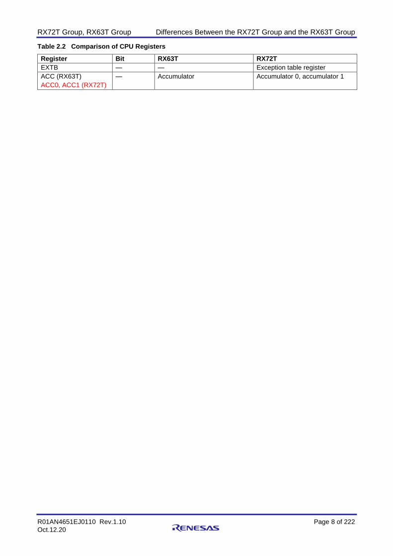
Table 2.2 Comparison of CPU Registers
Register Bit RX63T RX72T
EXTB — — Exception table register
ACC (RX63T)
ACC0, ACC1 (RX72T)
— Accumulator Accumulator 0, accumulator 1

RX72T Group, RX63T Group Differences Between the RX72T Group and the RX63T Group
R01AN4651EJ0110 Rev.1.10 Page 9 of 222
Oct.12.20
2.2 Operating Modes
Table 2.3 is a comparative overview of operating modes, and Table 2.4 is a comparison of operating mode–related registers.
Table 2.3 Comparative Overview of Operating Modes
Item
RX63T
RX72T
144-, 120-, 112-, and
100-Pin Versions 64- and 48-Pin Versions
Selection of operating
modes by mode-setting
pins on release from
reset state
Single-chip mode Single-chip mode Single-chip mode
Boot mode Boot mode Boot mode
(SCI interface)
USB boot mode ⎯ Boot mode
(USB interface)
⎯ ⎯ Boot mode
(FINE interface)
User boot mode ⎯ User boot mode
Selection of operating
modes by register
settings
Single-chip mode Single-chip mode Single-chip mode
User boot mode ⎯ User boot mode
On-chip ROM disabled
extended mode
⎯ On-chip ROM disabled
extended mode
On-chip ROM enabled
extended mode
⎯ On-chip ROM enabled
extended mode
Selection of endian
order
Single-chip mode: MDES
(endian select register S)
User boot mode: MDEB
(endian select register B)
Single-chip mode: MDES
(endian select register S)
MDE register
Table 2.4 Comparison of Operating Mode–Related Registers
Register Bit
RX63T
RX72T
144-, 120-, 112-, and
100-Pin Versions 64- and 48-Pin Versions
MDSR ⎯ Mode status register ⎯ Mode status register
SYSCR0 EXBE External bus enable bit ⎯ External bus enable bit
SYSCR1 ⎯ System control register 1 System control register
1
Initial values after a reset are different.
ECCRAME ⎯ ⎯ ECCRAM enable bit
VOLSR ⎯ ⎯ ⎯ Voltage level setting
register

RX72T Group, RX63T Group Differences Between the RX72T Group and the RX63T Group
R01AN4651EJ0110 Rev.1.10 Page 10 of 222
Oct.12.20
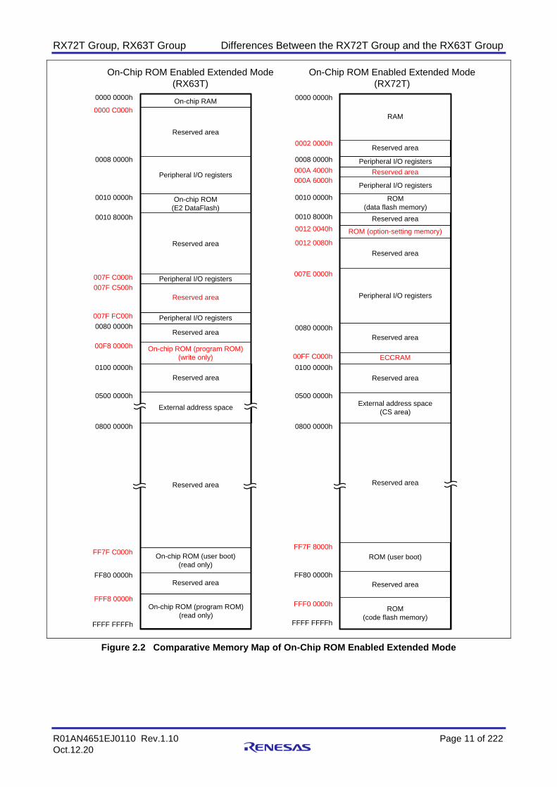
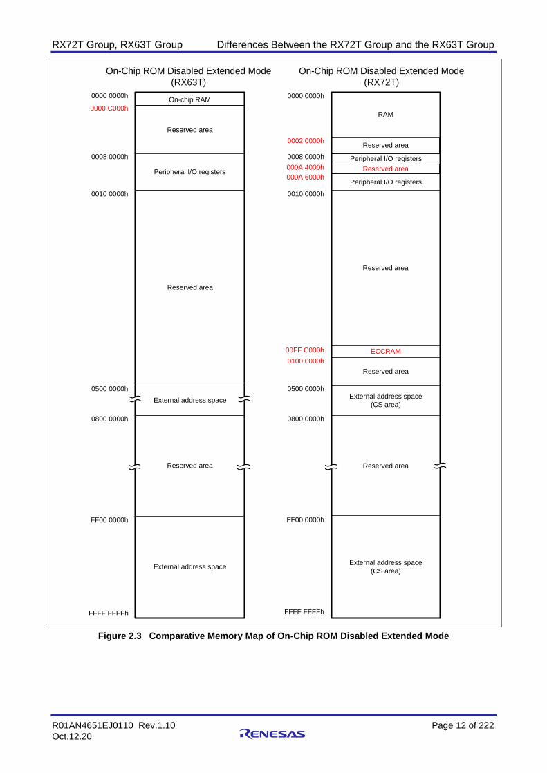
2.3 Address space
Figure 2.1 is a comparative memory map of single-chip mode, Figure 2.2 is a comparative memory map of on-chip ROM enabled extended mode, and Figure 2.3 is a comparative memory map of on-chip ROM disabled extended mode.
Single-chip mode (RX63T) Single-chip mode (RX72T)
0000 0000h
FFFF FFFFh
FFF0 0000h
007E 0000h
FF80 0000h
0080 0000h
0012 0080h
00FF C000h
FF7F 8000h
0010 0000h
000A 6000h
000A 4000h
0008 0000h
0002 0000h
0010 8000h
0012 0040h
0000 0000h
0008 0000h
FFFF FFFFh
0010 0000h
0010 8000h
0080 0000h
FFF8 0000h
007F C000h
007F C500h
007F FC00h
0000 C000h
00F8 0000h
FF7F C000h
FF80 0000h
0100 0000h
Reserved area
Reserved area
Reserved area
ROM (option-setting memory)
ECCRAM
Reserved area
Reserved area
Peripheral I/O registers
Reserved area
RAM
ROM
(code flash memory)
Peripheral I/O registers
ROM (user boot)
Reserved area
ROM(data flash memory)
Peripheral I/O registers
Reserved area
Reserved area
Reserved area
Reserved area
Reserved area
Reserved area
On-chip RAM
On-chip ROM (program ROM)
(read only)
Peripheral I/O registers
On-chip ROM
(E2 DataFlash)
On-chip ROM (program ROM)
(write only)
On-chip ROM (user boot)
(read only)
Peripheral I/O registers
Peripheral I/O registers
0100 0000h
Figure 2.1 Comparative Memory Map of Single-Chip Mode
RX72T Group, RX63T Group Differences Between the RX72T Group and the RX63T Group
R01AN4651EJ0110 Rev.1.10 Page 11 of 222
Oct.12.20
External address space
Reserved area
External address space
(CS area)
Reserved area
On-Chip ROM Enabled Extended Mode
(RX63T)
On-Chip ROM Enabled Extended Mode
(RX72T)
0000 0000h
FFFF FFFFh
FFF0 0000h
007E 0000h
FF80 0000h
0080 0000h
0012 0080h
00FF C000h
FF7F 8000h
0010 0000h
000A 6000h
000A 4000h
0008 0000h
0002 0000h
0010 8000h
0012 0040h
0000 0000h
0008 0000h
FFFF FFFFh
0010 0000h
0010 8000h
0080 0000h
FFF8 0000h
007F C000h
007F C500h
007F FC00h
0000 C000h
00F8 0000h
FF7F C000h
FF80 0000h
0100 0000h
Reserved area
Reserved area
Reserved area
ROM (option-setting memory)
ECCRAM
Reserved area
Reserved area
Peripheral I/O registers
Reserved area
RAM
ROM
(code flash memory)
Peripheral I/O registers
ROM (user boot)
Reserved area
ROM
(data flash memory)
Peripheral I/O registers
Reserved area
Reserved area
Reserved area
Reserved area
Reserved area
Reserved area
On-chip RAM
On-chip ROM (program ROM)
(read only)
Peripheral I/O registers
On-chip ROM
(E2 DataFlash)
On-chip ROM (program ROM)
(write only)
On-chip ROM (user boot)
(read only)
Peripheral I/O registers
Peripheral I/O registers
0100 0000h
0500 0000h
0800 0000h0800 0000h
0500 0000h
Figure 2.2 Comparative Memory Map of On-Chip ROM Enabled Extended Mode
RX72T Group, RX63T Group Differences Between the RX72T Group and the RX63T Group
R01AN4651EJ0110 Rev.1.10 Page 12 of 222
Oct.12.20
External address space
Reserved area
External address space
(CS area)
Reserved area
On-Chip ROM Disabled Extended Mode
(RX63T)
On-Chip ROM Disabled Extended Mode
(RX72T)
0000 0000h
FFFF FFFFh
00FF C000h
FF00 0000h
0010 0000h
000A 6000h
000A 4000h
0008 0000h
0002 0000h
0000 0000h
0008 0000h
FFFF FFFFh
0010 0000h
0000 C000h
FF00 0000h
0100 0000h
Reserved area
Reserved area
ECCRAM
Reserved area
Peripheral I/O registers
Reserved area
RAM
External address space
(CS area)
Peripheral I/O registers
External address space
Reserved area
Reserved area
On-chip RAM
Peripheral I/O registers
0500 0000h
0800 0000h0800 0000h
0500 0000h
Figure 2.3 Comparative Memory Map of On-Chip ROM Disabled Extended Mode

RX72T Group, RX63T Group Differences Between the RX72T Group and the RX63T Group
R01AN4651EJ0110 Rev.1.10 Page 13 of 222
Oct.12.20
2.4 Option-Setting Memory
Figure 2.4 is a comparison of option-setting memory areas, and Table 2.5 is a comparison of option-setting memory registers.
Option-setting memory (RX72T)
Option-setting memory (RX63T)
Address
Endian select register B (MDEB)
(user boot mode)
4 bytes
Option function select register 0 (OFS0)
Endian select register S (MDES)
(single-chip mode)
Option function select register 1 (OFS1)
UB code B
UB code A
Reserved area
Serial programmer command control
register (SPCC)
0012 0040h to 0012 0043h
0012 0050h to 0012 005Fh
0012 0044h to 0012 0047h
OCD/serial programmer ID setting register
(OSIS)
TM identification data register (TMINF)0012 0060h to 0012 0063h
Endian select register (MDE)
Option function select register 0 (OFS0)
Option function select register 1 (OFS1)
0012 0064h to 0012 0067h
0012 0068h to 0012 006Bh
0012 006Ch to 0012 006Fh
Reserved area
0012 0070h to 0012 007Bh
0012 0000h to 0012 003Fh
Address
UB code AFF7F FFE8h to FF7F FFEFh
UB code BFF7F FFF0h to FF7F FFF7h
4 bytes
Configuration setting area
User boot area
Reserved area
TM enable flag register (TMEF)
Reserved area
0012 0048h to 0012 004Bh
0012 004Ch to 0012 004Fh
0012 007Ch to 0012 007Fh ROM code protection register
(ROMCODE)
FF7F FFE8h to FF7F FFEFh
FF7F FFF0h to FF7F FFF7h
FF7F FFF8h to FF7F FFFBh
FFFF FF80h to FFFF FF83h
FFFF FF88h to FFFF FF8Bh
FFFF FF8Ch to FFFF FF8Fh
Figure 2.4 Comparison of Option-Setting Memory Areas

RX72T Group, RX63T Group Differences Between the RX72T Group and the RX63T Group
R01AN4651EJ0110 Rev.1.10 Page 14 of 222
Oct.12.20
Table 2.5 Comparison of Option-Setting Memory Registers
Register Bit RX63T RX72T (OFSM)
SPCC ⎯ ⎯ Serial programmer command
control register
OSIS ⎯ ⎯ OCD/serial programmer ID setting
register
OFS0 IWDTRSTIRQS IWDT reset interrupt request select
bit
0: Non-maskable interrupt requests
are enabled.
1: Resets are enabled.
IWDT reset interrupt request select
bit
0: Non-maskable interrupt requests
or plain interrupt requests are
enabled.
1: Resets are enabled.
WDTRSTIRQS WDT reset interrupt request select
bit
0: Non-maskable interrupt requests
are enabled.
1: Resets are enabled.
WDT reset interrupt request select
bit
0: Non-maskable interrupt requests
or plain interrupt requests are
enabled.
1: Resets are enabled.
OFS1 VDSEL ⎯ Voltage detection 0 level select bit
HOCOEN ⎯ HOCO oscillation enable bit
MDES ⎯ Endian select register S
(single-chip mode)
⎯
MDEB ⎯ Endian select register B
(user boot mode)
⎯
MDE ⎯ ⎯ Endian select register
TMEF ⎯ ⎯ TM enable flag register
TMINF ⎯ ⎯ TM identification data register
ROMCODE ⎯ ⎯ ROM code protection register

RX72T Group, RX63T Group Differences Between the RX72T Group and the RX63T Group
R01AN4651EJ0110 Rev.1.10 Page 15 of 222
Oct.12.20
2.5 Voltage Detection Circuit
Table 2.6 is a comparative overview of voltage detection circuit, and Table 2.7 is a comparison of voltage detection circuit registers.
In addition, Table 2.8 is a comparative listing of setting procedures for Vdet1 monitoring, Table 2.9 a comparative listing of setting procedures for Vdet2 monitoring, Table 2.10 a comparative listing of setting procedures for voltage monitoring 1 interrupt and voltage monitoring 1 reset–related bit operation, and Table 2.11 a comparative listing of setting procedures for voltage monitoring 2 interrupt and voltage monitoring 2 reset–related bit operation.
Table 2.6 Comparative Overview of Voltage Detection Circuit
Item
RX63T (LVDA) RX72T (LVDA)
Voltage
Monitoring 0
Voltage
Monitoring 1
Voltage
Monitoring 2
Voltage
Monitoring 0
Voltage
Monitoring 1
Voltage
Monitoring 2
VCC
monitoring
Monitored
voltage
Vdet0 Vdet1 Vdet2 Vdet0 Vdet1 Vdet2
Detected
event
Voltage drops
past Vdet0.
Voltage rises
or drops past
Vdet1.
Voltage rises
or drops past
Vdet2.
Voltage drops
past Vdet0.
Voltage rises
or drops past
Vdet1.
Voltage rises
or drops past
Vdet2.
Detection
voltage
One level,
fixed
Voltage
specified by
LVDLVLR.LVD
1LVL[3:0] bits
[144-, 120-,
112-, and 100-
pin versions]
Selectable
among three
different levels
[64- and 48-pin
versions]
One level,
fixed
Voltage
specified by
LVDLVLR.LVD
2LVL[3:0] bits
[144-, 120-,
112-, and 100-
pin versions]
Selectable
among three
different levels
[64- and 48-pin
versions]
One level,
fixed
Selectable
between two
different levels
using
OFS1.VDSEL
[1:0] bits
Selectable
between five
different levels
using
LVDLVLR.
LVD1LVL[3:0]
bits
Selectable
between five
different levels
using
LVDLVLR.
LVD2LVL[3:0]
bits
Monitoring
flag
No LVD1SR.LVD1
MON flag:
Monitors
whether
voltage is
higher or lower
than Vdet1.
LVD2SR.LVD2
MON flag:
Monitors
whether
voltage is
higher or lower
than Vdet2.
No LVD1SR.LVD1
MON flag:
Monitors
whether
voltage is
higher or lower
than Vdet1.
LVD2SR.LVD2
MON flag:
Monitors
whether
voltage is
higher or lower
than Vdet2.
LVD1SR.LVD1
DET flag:
Vdet1 passage
detection
LVD2SR.LVD2
DET flag:
Vdet2 passage
detection
LVD1SR.LVD1
DET flag:
Vdet1 passage
detection
LVD2SR.LVD2
DET flag:
Vdet2 passage
detection
Processing
upon
voltage
detection
Reset Voltage
monitoring 0
reset
Voltage
monitoring 1
reset
Voltage
monitoring 2
reset
Voltage
monitoring 0
reset
Voltage
monitoring 1
reset
Voltage
monitoring 2
reset
Reset when
Vdet0 > VCC;
CPU restart
after specified
duration of
VCC > Vdet0
Reset when
Vdet1 > VCC;
CPU restart
timing
selectable:
after specified
duration of
VCC > Vdet1
or after
specified
duration of
Vdet1 > VCC
Reset when
Vdet2 > VCC;
CPU restart
timing
selectable:
after specified
duration of
VCC > Vdet2
or after
specified
duration of
Vdet2 > VCC
Reset when
Vdet0 > VCC;
CPU restart
after specified
duration of
VCC > Vdet0
Reset when
Vdet1 > VCC;
CPU restart
timing
selectable:
after specified
duration of
VCC > Vdet1
or after
specified
duration of
Vdet1 > VCC
Reset when
Vdet2 > VCC;
CPU restart
timing
selectable:
after specified
duration of
VCC > Vdet2
or after
specified
duration of
Vdet2 > VCC

RX72T Group, RX63T Group Differences Between the RX72T Group and the RX63T Group
R01AN4651EJ0110 Rev.1.10 Page 16 of 222
Oct.12.20
Item
RX63T (LVDA) RX72T (LVDA)
Voltage
Monitoring 0
Voltage
Monitoring 1
Voltage
Monitoring 2
Voltage
Monitoring 0
Voltage
Monitoring 1
Voltage
Monitoring 2
Processing
upon
voltage
detection
Interrupt No Voltage
monitoring 1
interrupt
Voltage
monitoring 2
interrupt
No Voltage
monitoring 1
interrupt
Voltage
monitoring 2
interrupt
Non-maskable
interrupt
Non-maskable
interrupt
Non-maskable
interrupt or
maskable
interrupt,
selectable
Non-maskable
interrupt or
maskable
interrupt,
selectable
Interrupt
request both
when Vdet1 >
VCC and when
VCC > Vdet1,
or when one or
the other
occurs
Interrupt
request both
when Vdet2 >
VCC and when
VCC > Vdet2,
or when one or
the other
occurs
Interrupt
request both
when Vdet1 >
VCC and when
VCC > Vdet1,
or when one or
the other
occurs
Interrupt
request both
when Vdet2 >
VCC and when
VCC > Vdet2,
or when one or
the other
occurs
Digital filter Enabled/
disabled
switching
No digital filter
function
Yes Yes No digital filter
function
Yes Yes
Sampling
time
⎯ 1/n LOCO
frequency 2
(n: 1, 2, 4, 8)
1/n LOCO
frequency 2
(n: 1, 2, 4, 8)
⎯ 1/n LOCO
frequency 2
(n: 2, 4, 8, 16)
1/n LOCO
frequency 2
(n: 2, 4, 8, 16)
Event link function ⎯ ⎯ ⎯ No Yes
Output of
event signal at
detection of
Vdet passage
Yes
Output of
event signal at
detection of
Vdet passage

RX72T Group, RX63T Group Differences Between the RX72T Group and the RX63T Group
R01AN4651EJ0110 Rev.1.10 Page 17 of 222
Oct.12.20
Table 2.7 Comparison of Voltage Detection Circuit Registers
Register Bit
RX63T (LVDA)
RX72T (LVDA)
144-, 120-, 112-, and
100-Pin Versions
64- and 48-Pin
Versions
LVD1CR1 LVD1IRQSEL ⎯ Voltage monitoring 1
interrupt type select bit
LVD2CR1 LVD2IRQSEL ⎯ Voltage monitoring 2
interrupt type select bit
LVDLVLR LVD1LVL
[3:0]
Voltage detection 1
level select bits
(standard voltage
during drop in voltage)
[3 V products]
b3 b0
1 0 0 0: 2.90 V
1 0 0 1: 2.85 V
1 0 1 0: 2.88 V
Settings other than the
above are prohibited.
[5 V products]
b3 b0
1 0 0 0: 4.77 V
1 0 0 1: 4.23 V
1 0 1 0: 4.50 V
Settings other than the
above are prohibited.
Voltage detection 1
level select bits
(standard voltage
during drop in voltage)
b3 b0
1 0 1 0: 2.95 V
Settings other than the
above are prohibited.
Voltage detection 1 level
select bits (standard
voltage during drop in
voltage)
b3 b0
0 1 0 0: 4.57 V (Vdet1_0)
0 1 0 1: 4.47 V (Vdet1_1)
0 1 1 0: 4.32 V (Vdet1_2)
1 0 1 0: 2.93 V (Vdet1_3)
1 0 1 1: 2.88 V (Vdet1_4)
Settings other than the
above are prohibited.
LVD2LVL
[3:0]
Voltage detection 2
level select bits
(standard voltage
during drop in voltage)
[3 V products]
b7 b4
1 0 0 0: 2.90 V
1 0 0 1: 2.85 V
1 0 1 0: 2.88 V
Settings other than the
above are prohibited.
[5 V products]
b7 b4
1 0 0 0: 4.77 V
1 0 0 1: 4.23 V
1 0 1 0: 4.50 V
Settings other than the
above are prohibited.
Voltage detection 2
level select bits
(standard voltage
during drop in voltage)
b7 b4
1 0 1 0: 2.95 V
Settings other than the
above are prohibited.
Voltage detection 2 level
select bits (standard
voltage during drop in
voltage)
b7 b4
0 1 0 0: 4.57 V (Vdet2_0)
0 1 0 1: 4.47 V (Vdet2_1)
0 1 1 0: 4.32 V (Vdet2_2)
1 0 1 0: 2.93 V (Vdet2_3)
1 0 1 1: 2.88 V (Vdet2_4)
Settings other than the
above are prohibited.

RX72T Group, RX63T Group Differences Between the RX72T Group and the RX63T Group
R01AN4651EJ0110 Rev.1.10 Page 18 of 222
Oct.12.20
Register Bit
RX63T (LVDA)
RX72T (LVDA)
144-, 120-, 112-, and
100-Pin Versions
64- and 48-Pin
Versions
LVD1CR0 LVD1FSAMP
[1:0]
Sampling clock select bits
b5 b4
0 0: 1/1 LOCO frequency
0 1: 1/2 LOCO frequency
1 0: 1/4 LOCO frequency
1 1: 1/8 LOCO frequency
Sampling clock select
bits
b5 b4
0 0: 1/2 LOCO frequency
0 1: 1/4 LOCO frequency
1 0: 1/8 LOCO frequency
1 1: 1/16 LOCO
frequency
LVD2CR0 LVD2FSAMP
[1:0]
Sampling clock select bits
b5 b4
0 0: 1/1 LOCO frequency
0 1: 1/2 LOCO frequency
1 0: 1/4 LOCO frequency
1 1: 1/8 LOCO frequency
Sampling clock select
bits
b5 b4
0 0: 1/2 LOCO frequency
0 1: 1/4 LOCO frequency
1 0: 1/8 LOCO frequency
1 1: 1/16 LOCO
frequency

RX72T Group, RX63T Group Differences Between the RX72T Group and the RX63T Group
R01AN4651EJ0110 Rev.1.10 Page 19 of 222
Oct.12.20
Table 2.8 Comparative Listing of Setting Procedures for Vdet1 Monitoring
Item RX63T (LVDA) RX72T (LVDA)
Setting procedure for
Vdet1 monitoring
1 Specify the detection voltage by
setting the LVDLVLR.LVD1LVL[3:0]
bits.
Specify the detection voltage by
setting the LVDLVLR.LVD1LVL[3:0]
bits.
2 • Digital filter is in use
Select the sampling clock for the digital filter by setting the LVD1CR0.LVD1FSAMP[1:0] bits.
• Digital filter not in use
Set the LVD1CR0.LVD1DFDIS bit to 1 (digital filter disabled).
Set LVCMPCR.LVD1E = 1 (voltage
detection 1 circuit enabled).
3 Set the LVD1CR0.LVD1CMPE bit to
1 (output of voltage monitoring 1
circuit comparison results enabled).
Wait for at least td(E-A) (LVD
operation stabilization time after
LVD is enabled).
4 • Digital filter is in use
Wait for at least one cycle of LOCO.
• Digital filter not in use
⎯ (No procedure)
• Digital filter is in use
Select the sampling clock for the digital filter by setting the LVD1CR0.LVD1FSAMP[1:0] bits.
• Digital filter not in use
⎯ (No procedure)
5 • Digital filter is in use
Clear the LVD1CR0.LVD1DFDIS bit to 0 (digital filter enabled).
• Digital filter not in use
⎯ (No procedure)
• Digital filter is in use
Set LVD1CR0.LVD1DFDIS = 0 (digital filter enabled).
• Digital filter not in use
⎯ (No procedure)
6 • Digital filter is in use
Wait for at least 2n + 3 cycles of LOCO (where n = 1, 2, 4, or 8, and the sampling clock for the digital filter is the LOCO frequency divided by n).
• Digital filter not in use
⎯ (No procedure)
• Digital filter is in use
Wait for at least 2n + 3 cycles of LOCO (where n = 2, 4, 8, or 16, and the sampling clock for the digital filter is the LOCO frequency divided by n).
• Digital filter not in use
⎯ (No procedure)
7 Set the LVCMPCR.LVD1E bit to 1
(voltage detection 1 circuit enabled).
Set LVD1CR0.LVD1CMPE = 1
(output of voltage monitoring 1
circuit comparison results enabled).

RX72T Group, RX63T Group Differences Between the RX72T Group and the RX63T Group
R01AN4651EJ0110 Rev.1.10 Page 20 of 222
Oct.12.20
Table 2.9 Comparative Listing of Setting Procedures for Vdet2 Monitoring
Item RX63T (LVDA) RX72T (LVDA)
Setting procedure for
Vdet2 monitoring
1 Specify the detection voltage by
setting the LVDLVLR.LVD2LVL[3:0]
bits.
Specify the detection voltage by
setting the LVDLVLR.LVD2LVL[3:0]
bits.
2 • Digital filter is in use
Select the sampling clock for the digital filter by setting the LVD2CR0.LVD2FSAMP[1:0] bits.
• Digital filter not in use
Set the LVD2CR0.LVD2DFDIS bit to 1 (digital filter disabled).
Set LVCMPCR.LVD2E = 1 (voltage
detection 2 circuit enabled).
3 Set the LVD2CR0.LVD2CMPE bit to
1 (output of voltage monitoring 2
circuit comparison results enabled).
Wait for at least td(E-A) (LVD
operation stabilization time after
LVD is enabled).
4 • Digital filter is in use
Wait for at least one cycle of LOCO.
• Digital filter not in use
⎯ (No procedure)
• Digital filter is in use
Select the sampling clock for the digital filter by setting the LVD2CR0.LVD2FSAMP[1:0] bits.
• Digital filter not in use
⎯ (No procedure)
5 • Digital filter is in use
Clear the LVD2CR0.LVD2DFDIS bit to 0 (digital filter enabled).
• Digital filter not in use
⎯ (No procedure)
• Digital filter is in use
Set LVD2CR0.LVD2DFDIS = 0 (digital filter enabled).
• Digital filter not in use
⎯ (No procedure)
6 • Digital filter is in use
Wait for at least 2n + 3 cycles of LOCO (where n = 1, 2, 4, or 8, and the sampling clock for the digital filter is the LOCO frequency divided by n).
• Digital filter not in use
⎯ (No procedure)
• Digital filter is in use
Wait for at least 2n + 3 cycles of LOCO (where n = 2, 4, 8, or 16, and the sampling clock for the digital filter is the LOCO frequency divided by n).
• Digital filter not in use
⎯ (No procedure)
7 Set the LVCMPCR.LVD2E bit to 1
(voltage detection 2 circuit enabled).
Set LVD2CR0.LVD2CMPE = 1
(output of voltage monitoring 2
circuit comparison results enabled).

RX72T Group, RX63T Group Differences Between the RX72T Group and the RX63T Group
R01AN4651EJ0110 Rev.1.10 Page 21 of 222
Oct.12.20
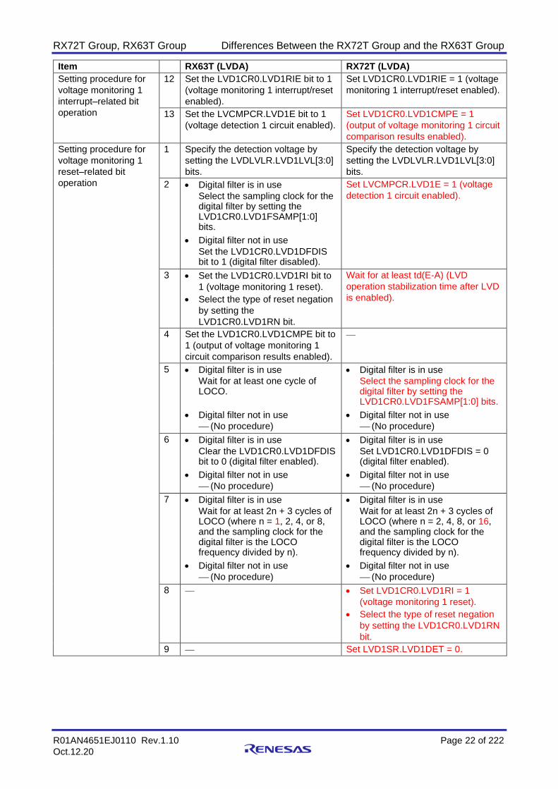
Table 2.10 Comparative Listing of Setting Procedures for Voltage Monitoring 1 Interrupt and Voltage
Monitoring 1 Reset–Related Bit Operation
Item RX63T (LVDA) RX72T (LVDA)
Setting procedure for
voltage monitoring 1
interrupt–related bit
operation
1 Specify the detection voltage by
setting the LVDLVLR.LVD1LVL[3:0]
bits.
Specify the detection voltage by
setting the LVDLVLR.LVD1LVL[3:0]
bits.
2 • Digital filter is in use
Select the sampling clock for the digital filter by setting the LVD1CR0.LVD1FSAMP[1:0] bits.
• Digital filter not in use
Set the LVD1CR0.LVD1DFDIS bit to 1 (digital filter disabled).
Set LVCMPCR.LVD1E = 1 (voltage
detection 1 circuit enabled).
3 Clear the LVD1CR0.LVD1RI bit to 0
(voltage monitoring 1 interrupt).
Wait for at least td(E-A) (LVD
operation stabilization time after LVD
is enabled).
4 Select the timing of interrupt
requests by setting the
LVD1CR1.LVD1IDTSEL[1:0] bits.
⎯
5 Set the LVD1CR0.LVD1CMPE bit to
1 (output of voltage monitoring 1
circuit comparison results enabled).
⎯
6 • Digital filter is in use
Wait for at least one cycle of LOCO.
• Digital filter not in use
⎯ (No procedure)
• Digital filter is in use
Select the sampling clock for the digital filter by setting the LVD1CR0.LVD1FSAMP[1:0] bits.
• Digital filter not in use
⎯ (No procedure)
7 • Digital filter is in use
Clear the LVD1CR0.LVD1DFDIS bit to 0 (digital filter enabled).
• Digital filter not in use
⎯ (No procedure)
• Digital filter is in use
Set LVD1CR0.LVD1DFDIS = 0 (digital filter enabled).
• Digital filter not in use
⎯ (No procedure)
8 • Digital filter is in use
Wait for at least 2n + 3 cycles of LOCO (where n = 1, 2, 4, or 8, and the sampling clock for the digital filter is the LOCO frequency divided by n).
• Digital filter not in use
⎯ (No procedure)
• Digital filter is in use
Wait for at least 2n + 3 cycles of LOCO (where n = 2, 4, 8, or 16, and the sampling clock for the digital filter is the LOCO frequency divided by n).
• Digital filter not in use
⎯ (No procedure)
9 ⎯ Set LVD1CR0.LVD1RI = 0 (voltage
monitoring 1 interrupt).
10 ⎯ • Select the timing of interrupt
requests by setting the
LVD1CR1.LVD1IDTSEL[1:0] bits.
• Select the type of interrupt by
setting the
LVD1CR1.LVD1IRQSEL bit.
11 Clear the LVD1SR.LVD1DET flag to
0.
Set LVD1SR.LVD1DET = 0.
RX72T Group, RX63T Group Differences Between the RX72T Group and the RX63T Group
R01AN4651EJ0110 Rev.1.10 Page 22 of 222
Oct.12.20
Item RX63T (LVDA) RX72T (LVDA)
Setting procedure for
voltage monitoring 1
interrupt–related bit
operation
12 Set the LVD1CR0.LVD1RIE bit to 1
(voltage monitoring 1 interrupt/reset
enabled).
Set LVD1CR0.LVD1RIE = 1 (voltage
monitoring 1 interrupt/reset enabled).
13 Set the LVCMPCR.LVD1E bit to 1
(voltage detection 1 circuit enabled).
Set LVD1CR0.LVD1CMPE = 1
(output of voltage monitoring 1 circuit
comparison results enabled).
Setting procedure for
voltage monitoring 1
reset–related bit
operation
1 Specify the detection voltage by
setting the LVDLVLR.LVD1LVL[3:0]
bits.
Specify the detection voltage by
setting the LVDLVLR.LVD1LVL[3:0]
bits.
2 • Digital filter is in use
Select the sampling clock for the digital filter by setting the LVD1CR0.LVD1FSAMP[1:0] bits.
• Digital filter not in use
Set the LVD1CR0.LVD1DFDIS bit to 1 (digital filter disabled).
Set LVCMPCR.LVD1E = 1 (voltage
detection 1 circuit enabled).
3 • Set the LVD1CR0.LVD1RI bit to
1 (voltage monitoring 1 reset).
• Select the type of reset negation
by setting the
LVD1CR0.LVD1RN bit.
Wait for at least td(E-A) (LVD
operation stabilization time after LVD
is enabled).
4 Set the LVD1CR0.LVD1CMPE bit to
1 (output of voltage monitoring 1
circuit comparison results enabled).
⎯
5 • Digital filter is in use
Wait for at least one cycle of LOCO.
• Digital filter not in use
⎯ (No procedure)
• Digital filter is in use
Select the sampling clock for the digital filter by setting the LVD1CR0.LVD1FSAMP[1:0] bits.
• Digital filter not in use
⎯ (No procedure)
6 • Digital filter is in use
Clear the LVD1CR0.LVD1DFDIS bit to 0 (digital filter enabled).
• Digital filter not in use
⎯ (No procedure)
• Digital filter is in use
Set LVD1CR0.LVD1DFDIS = 0 (digital filter enabled).
• Digital filter not in use
⎯ (No procedure)
7 • Digital filter is in use
Wait for at least 2n + 3 cycles of LOCO (where n = 1, 2, 4, or 8, and the sampling clock for the digital filter is the LOCO frequency divided by n).
• Digital filter not in use
⎯ (No procedure)
• Digital filter is in use
Wait for at least 2n + 3 cycles of LOCO (where n = 2, 4, 8, or 16, and the sampling clock for the digital filter is the LOCO frequency divided by n).
• Digital filter not in use
⎯ (No procedure)
8 ⎯ • Set LVD1CR0.LVD1RI = 1
(voltage monitoring 1 reset).
• Select the type of reset negation
by setting the LVD1CR0.LVD1RN
bit.
9 ⎯ Set LVD1SR.LVD1DET = 0.
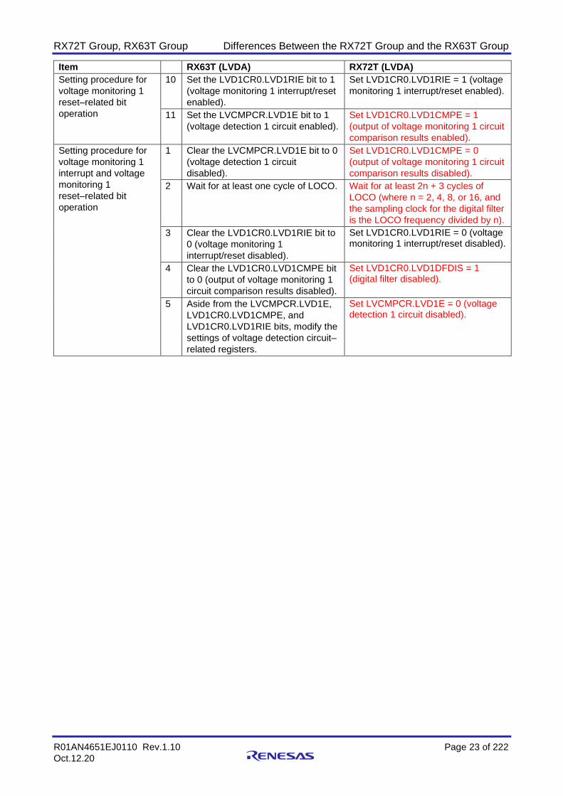
RX72T Group, RX63T Group Differences Between the RX72T Group and the RX63T Group
R01AN4651EJ0110 Rev.1.10 Page 23 of 222
Oct.12.20
Item RX63T (LVDA) RX72T (LVDA)
Setting procedure for
voltage monitoring 1
reset–related bit
operation
10 Set the LVD1CR0.LVD1RIE bit to 1
(voltage monitoring 1 interrupt/reset
enabled).
Set LVD1CR0.LVD1RIE = 1 (voltage
monitoring 1 interrupt/reset enabled).
11 Set the LVCMPCR.LVD1E bit to 1
(voltage detection 1 circuit enabled).
Set LVD1CR0.LVD1CMPE = 1
(output of voltage monitoring 1 circuit
comparison results enabled).
Setting procedure for
voltage monitoring 1
interrupt and voltage
monitoring 1
reset–related bit
operation
1 Clear the LVCMPCR.LVD1E bit to 0
(voltage detection 1 circuit
disabled).
Set LVD1CR0.LVD1CMPE = 0
(output of voltage monitoring 1 circuit
comparison results disabled).
2 Wait for at least one cycle of LOCO. Wait for at least 2n + 3 cycles of
LOCO (where n = 2, 4, 8, or 16, and
the sampling clock for the digital filter
is the LOCO frequency divided by n).
3 Clear the LVD1CR0.LVD1RIE bit to
0 (voltage monitoring 1
interrupt/reset disabled).
Set LVD1CR0.LVD1RIE = 0 (voltage monitoring 1 interrupt/reset disabled).
4 Clear the LVD1CR0.LVD1CMPE bit
to 0 (output of voltage monitoring 1
circuit comparison results disabled).
Set LVD1CR0.LVD1DFDIS = 1 (digital filter disabled).
5 Aside from the LVCMPCR.LVD1E,
LVD1CR0.LVD1CMPE, and
LVD1CR0.LVD1RIE bits, modify the
settings of voltage detection circuit–
related registers.
Set LVCMPCR.LVD1E = 0 (voltage detection 1 circuit disabled).

RX72T Group, RX63T Group Differences Between the RX72T Group and the RX63T Group
R01AN4651EJ0110 Rev.1.10 Page 24 of 222
Oct.12.20
Table 2.11 Comparative Listing of Setting Procedures for Voltage Monitoring 2 Interrupt and Voltage
Monitoring 2 Reset–Related Bit Operation
Item RX63T (LVDA) RX72T (LVDA)
Setting procedure for
voltage monitoring 2
interrupt–related bit
operation
1 Specify the detection voltage by
setting the LVDLVLR.LVD2LVL[3:0]
bits.
Specify the detection voltage by
setting the LVDLVLR.LVD2LVL[3:0]
bits.
2 • Digital filter is in use
Select the sampling clock for the digital filter by setting the LVD2CR0.LVD2FSAMP[1:0] bits.
• Digital filter not in use
Set the LVD2CR0.LVD2DFDIS bit to 1 (digital filter disabled).
Set LVCMPCR.LVD2E = 1 (voltage
detection 2 circuit enabled).
3 Clear the LVD2CR0.LVD2RI bit to 0
(voltage monitoring 2 interrupt).
Wait for at least td(E-A) (LVD
operation stabilization time after LVD
is enabled).
4 Select the timing of interrupt
requests by setting the
LVD2CR1.LVD2IDTSEL[1:0] bits.
⎯
5 Set the LVD2CR0.LVD2CMPE bit to
1 (output of voltage monitoring 2
circuit comparison results enabled).
⎯
6 • Digital filter is in use
Wait for at least one cycle of LOCO.
• Digital filter not in use
⎯ (No procedure)
• Digital filter is in use
Select the sampling clock for the digital filter by setting the LVD2CR0.LVD2FSAMP[1:0] bits.
• Digital filter not in use
⎯ (No procedure)
7 • Digital filter is in use
Clear the LVD2CR0.LVD2DFDIS bit to 0 (digital filter enabled).
• Digital filter not in use
⎯ (No procedure)
• Digital filter is in use
Set LVD2CR0.LVD2DFDIS = 0 (digital filter enabled).
• Digital filter not in use
⎯ (No procedure)
8 • Digital filter is in use
Wait for at least 2n + 3 cycles of LOCO (where n = 1, 2, 4, or 8, and the sampling clock for the digital filter is the LOCO frequency divided by n).
• Digital filter not in use
⎯ (No procedure)
• Digital filter is in use
Wait for at least 2n + 3 cycles of LOCO (where n = 2, 4, 8, or 16, and the sampling clock for the digital filter is the LOCO frequency divided by n).
• Digital filter not in use
⎯ (No procedure)
9 ⎯ Set LVD2CR0.LVD2RI = 0 (voltage
monitoring 2 interrupt).
10 ⎯ • Select the timing of interrupt
requests by setting the
LVD2CR1.LVD2IDTSEL[1:0] bits.
• Select the type of interrupt by
setting the
LVD2CR1.LVD2IRQSEL bit.
11 Clear the LVD2SR.LVD2DET flag to
0.
Set LVD2SR.LVD2DET = 0.

RX72T Group, RX63T Group Differences Between the RX72T Group and the RX63T Group
R01AN4651EJ0110 Rev.1.10 Page 25 of 222
Oct.12.20
Item RX63T (LVDA) RX72T (LVDA)
Setting procedure for
voltage monitoring 2
interrupt–related bit
operation
12 Set the LVD2CR0.LVD2RIE bit to 1
(voltage monitoring 2 interrupt/reset
enabled).
Set LVD2CR0.LVD2RIE = 1 (voltage
monitoring 2 interrupt/reset enabled).
13 Set the LVCMPCR.LVD2E bit to 1
(voltage detection 2 circuit enabled).
Set LVD2CR0.LVD2CMPE = 1
(output of voltage monitoring 2 circuit
comparison results enabled).
Setting procedure for
voltage monitoring 2
reset–related bit
operation
1 Specify the detection voltage by
setting the LVDLVLR.LVD2LVL[3:0]
bits.
Specify the detection voltage by
setting the LVDLVLR.LVD2LVL[3:0]
bits.
2 • Digital filter is in use
Select the sampling clock for the digital filter by setting the LVD2CR0.LVD2FSAMP[1:0] bits.
• Digital filter not in use
Set the LVD2CR0.LVD2DFDIS bit to 1 (digital filter disabled).
Set LVCMPCR.LVD2E = 1 (voltage
detection 2 circuit enabled).
3 • Set the LVD2CR0.LVD2RI bit to
1 (voltage monitoring 2 reset).
• Select the type of reset negation
by setting the
LVD2CR0.LVD2RN bit.
Wait for at least td(E-A) (LVD
operation stabilization time after LVD
is enabled).
4 Set the LVD2CR0.LVD2CMPE bit to
1 (output of voltage monitoring 2
circuit comparison results enabled).
⎯
5 • Digital filter is in use
Wait for at least one cycle of LOCO.
• Digital filter not in use
⎯ (No procedure)
• Digital filter is in use
Select the sampling clock for the digital filter by setting the LVD2CR0.LVD2FSAMP[1:0] bits.
• Digital filter not in use
⎯ (No procedure)
6 • Digital filter is in use
Clear the LVD2CR0.LVD2DFDIS bit to 0 (digital filter enabled).
• Digital filter not in use
⎯ (No procedure)
• Digital filter is in use
Set LVD2CR0.LVD2DFDIS = 0 (digital filter enabled).
• Digital filter not in use
⎯ (No procedure)
7 • Digital filter is in use
Wait for at least 2n + 3 cycles of LOCO (where n = 1, 2, 4, or 8, and the sampling clock for the digital filter is the LOCO frequency divided by n).
• Digital filter not in use
⎯ (No procedure)
• Digital filter is in use
Wait for at least 2n + 3 cycles of LOCO (where n = 2, 4, 8, or 16, and the sampling clock for the digital filter is the LOCO frequency divided by n).
• Digital filter not in use
⎯ (No procedure)
8 ⎯ • Set LVD2CR0.LVD2RI = 1
(voltage monitoring 2 reset).
• Select the type of reset negation
by setting the LVD2CR0.LVD2RN
bit.
9 ⎯ Set LVD2SR.LVD2DET = 0.

RX72T Group, RX63T Group Differences Between the RX72T Group and the RX63T Group
R01AN4651EJ0110 Rev.1.10 Page 26 of 222
Oct.12.20
Item RX63T (LVDA) RX72T (LVDA)
Setting procedure for
voltage monitoring 2
reset–related bit
operation
10 Set the LVD2CR0.LVD2RIE bit to 1
(voltage monitoring 2 interrupt/reset
enabled).
Set LVD2CR0.LVD2RIE = 1 (voltage
monitoring 2 interrupt/reset enabled).
11 Set the LVCMPCR.LVD2E bit to 1
(voltage detection 2 circuit enabled).
Set LVD2CR0.LVD2CMPE = 1
(output of voltage monitoring 2 circuit
comparison results enabled).
Setting procedure for
voltage monitoring 2
interrupt and voltage
monitoring 2
reset–related bit
operation
1 Clear the LVCMPCR.LVD2E bit to 0
(voltage detection 2 circuit
disabled).
Set LVD2CR0.LVD2CMPE = 0
(output of voltage monitoring 2 circuit
comparison results disabled).
2 Wait for at least one cycle of LOCO. Wait for at least 2n + 3 cycles of
LOCO (where n = 2, 4, 8, or 16, and
the sampling clock for the digital filter
is the LOCO frequency divided by n).
3 Clear the LVD2CR0.LVD2RIE bit to
0 (voltage monitoring 2
interrupt/reset disabled).
Set LVD2CR0.LVD2RIE = 0 (voltage monitoring 2 interrupt/reset disabled).
4 Clear the LVD2CR0.LVD2CMPE bit
to 0 (output of voltage monitoring 2
circuit comparison results disabled).
Set LVD2CR0.LVD2DFDIS = 1 (digital filter disabled).
5 Aside from the LVCMPCR.LVD2E,
LVD2CR0.LVD2CMPE, and
LVD2CR0.LVD2RIE bits, modify the
settings of voltage detection circuit–
related registers.
Set LVCMPCR.LVD2E = 0 (voltage detection 2 circuit disabled).

RX72T Group, RX63T Group Differences Between the RX72T Group and the RX63T Group
R01AN4651EJ0110 Rev.1.10 Page 27 of 222
Oct.12.20
2.6 Clock Generation Circuit
Table 2.12 is a comparative overview of clock generation circuit, and Table 2.13 is a comparison of clock generation circuit registers.
Table 2.12 Comparative Overview of Clock Generation Circuit
Item
RX63T
RX72T
144-, 120-, 112- and
100-Pin Versions
64- and 48-Pin
Versions
Use • Generates the system clock (ICLK)
supplied to the CPU, DMAC, DTC, ROM,
and RAM.
• Generates the peripheral module clock
(PCLKA) supplied to the MTU3, GPT and
DPC.
• Generates the peripheral module clock
(PCLKB) supplied to the peripheral
modules.
• Generates the AD clock (PCLKC) supplied
to the AD.
• Generates the S12AD clock (PCLKD)
supplied to the S12AD.
• Generates the FlashIF clock (FCLK)
supplied to the FlashIF.
• Generates the external bus clock (BCLK)
supplied to the external bus.
• Generates the USB clock (UCLK) supplied
to the USB.
• Generates the CAC clock (CACMCLK)
supplied to the CAC.
• Generates the CAN clock (CANMCLK)
supplied to the CAN.
• Generates the IWDT-dedicated clock
(IWDTCLK) supplied to the IWDT.
• Generates the system clock (ICLK)
supplied to the CPU, DMAC, DTC,
code flash memory, and RAM.
• Generates the peripheral module
clock (PCLKA) supplied to the
RSPI, SCIi, MTU3 (internal
peripheral buses), GPTW (internal
peripheral buses), and HRPWM
(internal peripheral buses).
• Generates the peripheral module
clock (PCLKB) supplied to
peripheral modules.
• Generates the counter reference
clock for the peripheral module
supplied to the MTU3 and GPTW
and the reference clock (PCLKC) for
the HRPWM.
• Generates the peripheral module
clocks (for analog conversion)
(PCLKD) supplied to S12AD.
• Generates the flash-IF clock (FCLK)
supplied to the flash interface.
• Generates the external bus clock
(BCLK) supplied to the external bus.
• Generates the USB clock (UCLK)
supplied to the USBb.
• Generates the CAC clock
(CACCLK) supplied to the CAC.
• Generates the CAN clock
(CANMCLK) supplied to the CAN.
• Generates the IWDT-dedicated
clock (IWDTCLK) supplied to the
IWDT.

RX72T Group, RX63T Group Differences Between the RX72T Group and the RX63T Group
R01AN4651EJ0110 Rev.1.10 Page 28 of 222
Oct.12.20
Item
RX63T
RX72T
144-, 120-, 112- and
100-Pin Versions
64- and 48-Pin
Versions
Operating
frequency • ICLK: 100 MHz (max.)
• PCLKA: 100 MHz (max.)
• PCLKB: 50 MHz (max.)
• PCLKC: 100 MHz (max.)
• PCLKD: 50 MHz (max.)
• FCLK:
⎯ 4 MHz to 50 MHz
(for programming and erasing the
ROM and E2 DataFlash)
⎯ 50 MHz (max.)
(for reading from the E2 DataFlash)
• BCLK: 50 MHz (max.)
• BCLK pin output: 50 MHz (max.)
• UCLK: 48 MHz (max.)
• CACMCLK: Same as clocks from
respective oscillators.
• CANMCLK: 14 MHz (max.)
• IWDTCLK: 125 kHz
• ICLK: 200 MHz (max.)
• PCLKA: 120 MHz (max.)
• PCLKB: 60 MHz (max.)
• PCLKC: 200 MHz (max.)
• PCLKD: 8 MHz to 60 MHz (for
conversion with 12-bit A/D
converter)
• FCLK:
⎯ 4 MHz to 60 MHz
(for programming and erasing
the code flash memory and data
flash memory)
⎯ 60 MHz (max.)
(for reading from the data flash
memory)
• BCLK: 60 MHz (max.)
• BCLK pin output: 40 MHz (max.)
• UCLK: 48 MHz (max.)
• CACCLK: Same as clocks from
respective oscillators.
• CANMCLK: 24 MHz (max.)
• IWDTCLK: 120 kHz
Main clock
oscillator • Resonator
frequency:
8 MHz to
12.5 MHz
• External clock
input frequency:
14 MHz (max.)
• Connectable
resonator or
additional circuit:
ceramic
resonator, crystal
resonator
• Connection pins:
EXTAL, XTAL
• Oscillation stop
detection function:
When oscillation
stop is detected
on the main clock,
the system clock
source is switched
to LOCO, and
MTU and GPT
outputs can be
forcedly driven
high-impedance.
• Resonator
frequency:
4 MHz to 16 MHz
• External clock
input frequency:
20 MHz (max.)
• Connectable
resonator or
additional circuit:
ceramic
resonator, crystal
resonator
• Connection pins:
EXTAL, XTAL
• Oscillation stop
detection function:
When oscillation
stop is detected
on the main clock,
the system clock
source is switched
to LOCO, and
MTU and GPT
outputs can be
forcedly driven
high-impedance.
• Resonator frequency:
8 MHz to 24 MHz
• External clock input frequency:
24 MHz (max.)
• Connectable resonator or additional
circuit:
ceramic resonator, crystal resonator
• Connection pins:
EXTAL, XTAL
• Oscillation stop detection function:
When oscillation stop is detected on
the main clock, the system clock
source is switched to LOCO, and
MTU3 and GPTW output can be
forcedly driven high-impedance.

RX72T Group, RX63T Group Differences Between the RX72T Group and the RX63T Group
R01AN4651EJ0110 Rev.1.10 Page 29 of 222
Oct.12.20
Item
RX63T
RX72T
144-, 120-, 112- and
100-Pin Versions
64- and 48-Pin
Versions
PLL frequency
synthesizer • Input clock
source: Main
clock
• Input pulse
frequency division
ratio: Selectable
among 1, 2, and 4
• Input frequency:
8 MHz to 12.5
MHz
• Frequency
multiplication
ratio: Selectable
among 8, 10, 12,
16, 20, 24, 25,
and 50
• VCO oscillation
frequency: 104
MHz to 200 MHz
• Input clock
source: Main
clock
• Input pulse
frequency division
ratio: Selectable
among 1, 2, and 4
• Input frequency:
4 MHz to 16 MHz
• Frequency
multiplication
ratio: Selectable
among 8, 10, 12,
16, 20, 24, 25,
and 50
• VCO oscillation
frequency: 104
MHz to 200 MHz
• Input clock source:
Main clock, HOCO
• Input pulse frequency division ratio:
Selectable among 1, 2, and 3
• Input frequency:
8 MHz to 24 MHz
• Frequency multiplication ratio:
Selectable from 10 to 30
(in increments of 0.5)
• Output clock frequency of the PLL
frequency synthesizer: 120 MHz to
240 MHz
High-speed on-
chip oscillator
(HOCO)
— • Selectable among 16 MHz, 18 MHz,
and 20 MHz
• HOCO power supply control
Low-speed on-
chip oscillator
(LOCO)
Oscillation frequency: 125 kHz Oscillation frequency: 240 kHz
IWDT-dedicated
on-chip oscillator
Oscillation frequency: 125 kHz Oscillation frequency: 120 kHz
Control of output
on BCLK pin • Selectable between BCLK clock output or
high-level output
• Selectable between BCLK or BCLK/2
• Selectable between BCLK clock
output or high output
• Selectable between BCLK or
BCLK/2
Event link
function (output)
— Detection of stopping of the main clock
oscillator
Event link
function (input)
— Switching of the clock source to the
low-speed on-chip oscillator

RX72T Group, RX63T Group Differences Between the RX72T Group and the RX63T Group
R01AN4651EJ0110 Rev.1.10 Page 30 of 222
Oct.12.20
Table 2.13 Comparison of Clock Generation Circuit Registers
Register Bit RX63T RX72T
MEMWAIT — — Memory wait cycle setting register
SCKCR2 UCK[3:0] USB clock (UCLK) select bits
b7 b4
0 0 0 1: 1/2
0 0 1 0: 1/3
0 0 1 1: 1/4
Settings other than the above are
prohibited when the USB is in use.
When the USB is not in use, these
bits are read as 0001b. The write
value should be 0001b.
USB clock (UCLK) select bits
b7 b4
0 0 0 1: 1/2
0 0 1 0: 1/3
0 0 1 1: 1/4
0 1 0 0: 1/5
Settings other than the above are
prohibited when the USB is in use.
When the USB is not in use, these
bits are read as 0001b. The write
value should be 0001b.
SCKCR3 CKSEL[2:0] Clock source select bits
b10 b8
0 0 0: LOCO
0 1 0: Main clock oscillator
1 0 0: PLL circuit
Settings other than the above are
prohibited.
Clock source select bits
b10 b8
0 0 0: LOCO
0 0 1: HOCO
0 1 0: Main clock oscillator
1 0 0: PLL circuit
Settings other than the above are
prohibited.
PLLCR PLIDIV[1:0] PLL input frequency division ratio
select bits
b1 b0
0 0: 1
0 1: 1/2
1 0: 1/4
1 1: Setting prohibited.
PLL input frequency division ratio
select bits
b1 b0
0 0: 1
0 1: 1/2
1 0: 1/3
1 1: Setting prohibited.
PLLSRCSEL — PLL clock source select bit
STC[5:0] Frequency multiplication factor
select bits
b13 b8
0 0 0 1 1 1: 8
0 0 1 0 0 1: 10
0 0 1 0 1 1: 12
0 0 1 1 1 1: 16
0 1 0 0 1 1: 20
0 1 0 1 1 1: 24
0 1 1 0 0 0: 25
1 1 0 0 0 1: 50
Settings other than the above are
prohibited.
Frequency multiplication factor
select bits
b13 b8
0 1 0 0 1 1: 10.0
0 1 0 1 0 0: 10.5
0 1 0 1 0 1: 11.0
0 1 0 1 1 0: 11.5
0 1 0 1 1 1: 12.0
0 1 1 0 0 0: 12.5
:
1 1 1 0 0 1: 29.0
1 1 1 0 1 0: 29.5
1 1 1 0 1 1: 30.0
Settings other than the above are
prohibited.
HOCOCR — — High-speed on-chip oscillator
control register
HOCOCR2 — — High-speed on-chip oscillator
control register 2
OSCOVFSR — — Oscillation stabilization flag register

RX72T Group, RX63T Group Differences Between the RX72T Group and the RX63T Group
R01AN4651EJ0110 Rev.1.10 Page 31 of 222
Oct.12.20
Register Bit RX63T RX72T
MOSCWTCR — See 2.8, Low Power Consumption. Main clock oscillator wait control
register
MOFCR MOFXIN Main clock oscillator forced
oscillation bit
—
MODRV2[1:0] — Main clock oscillator driving ability 2
switching bits
MOSEL — Main clock oscillator switching bit
HOCOPCR — — High-speed on-chip oscillator power
supply control register

RX72T Group, RX63T Group Differences Between the RX72T Group and the RX63T Group
R01AN4651EJ0110 Rev.1.10 Page 32 of 222
Oct.12.20
2.7 Clock Frequency Accuracy Measurement Circuit
Table 2.14 is a comparative overview of clock frequency accuracy measurement circuit, and Table 2.15 is a comparison of clock frequency accuracy measurement circuit registers.
Table 2.14 Comparative Overview of Clock Frequency Accuracy Measurement Circuit
Item RX63T (CAC) RX72T (CAC)
Measurement
target clocks
The frequencies of the following clocks
can be measured:
• Clock output from main clock oscillator
(CACMCLK)
• IWDT-dedicated clock (IWDTCLK)
• Peripheral module clock (PCLK)
The frequencies of the following clocks
can be measured:
• Main clock
• HOCO clock
• LOCO clock
• IWDTCLK clock
• Peripheral module clock B (PCLKB)
Measurement
reference clocks • External clock input on CACREF pin
• Clock output from main clock oscillator
(CACMCLK)
• IWDT-dedicated clock (IWDTCLK)
• Peripheral module clock (PCLK)
• External clock input on CACREF pin
• Main clock
• HOCO clock
• LOCO clock
• IWDTCLK clock
• Peripheral module clock B (PCLKB)
Selectable
function
Digital filter function Digital filter function
Interrupt sources • Measurement end interrupt
• Frequency error interrupt
• Overflow
• Measurement end interrupt
• Frequency error interrupt
• Overflow interrupt
Low power
consumption
function
Ability to specify transition to module stop
state
Ability to specify transition to module stop
state

RX72T Group, RX63T Group Differences Between the RX72T Group and the RX63T Group
R01AN4651EJ0110 Rev.1.10 Page 33 of 222
Oct.12.20
Table 2.15 Comparison of Clock Frequency Accuracy Measurement Circuit Registers
Register Bit RX63T (CAC) RX72T (CAC)
CACR1 FMCS[2:0] Frequency measurement clock
select bits
b3 b1
0 0 0: Clock output from main clock
oscillator (CACMCLK)
0 0 1: Setting prohibited.
0 1 0: Setting prohibited.
0 1 1: Setting prohibited.
1 0 0: IWDT-dedicated clock
(IWDTCLK)
1 0 1: Peripheral module clock
(PCLK)
1 1 0: Setting prohibited.
1 1 1: Setting prohibited.
Measurement target clock select
bits
b3 b1
0 0 0: Main clock
0 1 0: HOCO clock
0 1 1: LOCO clock
1 0 0: IWDTCLK clock
1 0 1: Peripheral module clock B
(PCLKB)
Settings other than the above are
prohibited.
CACR2 RSCS[2:0] Reference signal generation clock
select bits
b3 b1
0 0 0: Clock output from main clock
oscillator (CACMCLK)
0 0 1: Setting prohibited.
0 1 0: Setting prohibited.
0 1 1: Setting prohibited.
1 0 0: IWDT-dedicated clock
(IWDTCLK)
1 0 1: Peripheral module clock
(PCLK)
1 1 0: Setting prohibited.
1 1 1: Setting prohibited.
Measurement reference clock
select bits
b3 b1
0 0 0: Main clock
0 1 0: HOCO clock
0 1 1: LOCO clock
1 0 0: IWDTCLK clock
1 0 1: Peripheral module clock B
(PCLKB)
Settings other than the above are
prohibited.

RX72T Group, RX63T Group Differences Between the RX72T Group and the RX63T Group
R01AN4651EJ0110 Rev.1.10 Page 34 of 222
Oct.12.20
2.8 Low Power Consumption
Table 2.16 is a comparison of procedures for entering and exiting low power consumption modes and operating states in each mode, and Table 2.17 is a comparison of low power consumption registers.
Table 2.16 Comparison of Procedures for Entering and Exiting Low Power Consumption Modes and
Operating States in Each Mode
Mode
Entering and Exiting Low Power
Consumption Modes and
Operating States RX63T RX72T
Sleep mode Transition method Control register
+ instruction
Control register
+ instruction
Method of cancellation other than reset Interrupt Interrupt
State after cancellation Program execution
state (interrupt
processing)
Program execution
state (interrupt
processing)
Main clock oscillator Operation possible Operation possible
High-speed on-chip oscillator ⎯ Operation possible
Low-speed on-chip oscillator Operation possible Operation possible
IWDT-dedicated on-chip oscillator Operation possible Operation possible
PLL Operation possible Operation possible
CPU Stopped (retained) Stopped (retained)
On-chip RAM0
(0000 0000h to 0000 BFFFh): RX63T
RAM, ECCRAM: RX72T
Operation (retained) Operation (retained)
Flash memory Operation Operation
USB 2.0 Host/Function module
(USBa: RX63T, USBb: RX72T)
Operation possible Operation possible
Watchdog timer (WDTA) Stopped (retained) Stopped (retained)
Independent watchdog timer (IWDTa) Operation possible Operation possible
Port output enable
(POE3: RX63T, POE3B: RX72T)
Operation possible Operation possible
8-bit timer (unit 0, unit 1) (TMR) ⎯ Operation possible
Voltage detection circuit (LVDA) Operation possible Operation possible
Power-on reset circuit Operation Operation
Peripheral modules Operation possible Operation possible
I/O ports Operation Operation
All-module
clock stop
mode
Transition method Control register
+ instruction
Control register
+ instruction
Method of cancellation other than reset Interrupt Interrupt
State after cancellation Program execution
state (interrupt
processing)
Program execution
state (interrupt
processing)
Main clock oscillator Operation possible Operation possible
High-speed on-chip oscillator ⎯ Operation possible
Low-speed on-chip oscillator Operation possible Operation possible
IWDT-dedicated on-chip oscillator Operation possible Operation possible
PLL Operation possible Operation possible
CPU Stopped (retained) Stopped (retained)
On-chip RAM0
(0000 0000h to 0000 BFFFh): RX63T
RAM, ECCRAM: RX72T
Stopped (retained) Stopped (retained)
Flash memory Stopped (retained) Stopped (retained)

RX72T Group, RX63T Group Differences Between the RX72T Group and the RX63T Group
R01AN4651EJ0110 Rev.1.10 Page 35 of 222
Oct.12.20
Mode
Entering and Exiting Low Power
Consumption Modes and
Operating States RX63T RX72T
All-module
clock stop
mode
USB 2.0 Host/Function module
(USBa: RX63T, USBb: RX72T)
Stopped Stopped
Watchdog timer (WDTA) Stopped (retained) Stopped (retained)
Independent watchdog timer (IWDTa) Operation possible Operation possible
Port output enable
(POE3: RX63T, POE3B: RX72T)
Operation possible*1 Operation possible*1
8-bit timer (unit 0, unit 1) (TMR) ⎯ Operation possible
Voltage detection circuit (LVDA) Operation possible Operation possible
Power-on reset circuit Operation Operation
Peripheral modules Stopped (retained) Stopped (retained)
I/O ports Retained Retained
Software
standby mode
Transition method Control register
+ instruction
Control register
+ instruction
Method of cancellation other than reset Interrupt Interrupt
State after cancellation Program execution
state (interrupt
processing)
Program execution
state (interrupt
processing)
Main clock oscillator Operation possible Stopped
High-speed on-chip oscillator ⎯ Stopped
Low-speed on-chip oscillator Stopped Stopped
IWDT-dedicated on-chip oscillator Operation possible Operation possible
PLL Stopped Stopped
CPU Stopped (retained) Stopped (retained)
On-chip RAM0
(0000 0000h to 0000 BFFFh): RX63T
RAM, ECCRAM: RX72T
Stopped (retained) Stopped (retained)
Flash memory Stopped (retained) Stopped (retained)
USB 2.0 Host/Function module
(USBa: RX63T, USBb: RX72T)
Stopped Stopped
Watchdog timer (WDTA) Stopped (retained) Stopped (retained)
Independent watchdog timer (IWDTa) Operation possible Operation possible
Port output enable
(POE3: RX63T, POE3B: RX72T)
Stopped (retained) Stopped (retained)
8-bit timer (unit 0, unit 1) (TMR) ⎯ Stopped (retained)
Voltage detection circuit (LVDA) Operation possible Operation possible
Power-on reset circuit Operation Operation
Peripheral modules Stopped (retained) Stopped (retained)
I/O ports Retained Retained
Deep software
standby mode
Transition method Control register
+ instruction
Control register
+ instruction
Method of cancellation other than reset Interrupt Interrupt
State after cancellation Program execution
state (reset
processing)
Program execution
state (reset
processing)
Main clock oscillator Operation possible Stopped
High-speed on-chip oscillator ⎯ Stopped
Low-speed on-chip oscillator Stopped Stopped
IWDT-dedicated on-chip oscillator Stopped (undefined) Stopped (undefined)
PLL Stopped Stopped
CPU Stopped (undefined) Stopped (undefined)

RX72T Group, RX63T Group Differences Between the RX72T Group and the RX63T Group
R01AN4651EJ0110 Rev.1.10 Page 36 of 222
Oct.12.20
Mode
Entering and Exiting Low Power
Consumption Modes and
Operating States RX63T RX72T
Deep software
standby mode
On-chip RAM0
(0000 0000h to 0000 BFFFh): RX63T
RAM, ECCRAM: RX72T
Stopped (undefined) Stopped (undefined)
Flash memory Stopped (retained) Stopped (retained)
USB 2.0 Host/Function module
(USBa: RX63T, USBb: RX72T)
Stopped (undefined) Stopped (undefined)
Watchdog timer (WDTA) Stopped (undefined) Stopped (undefined)
Independent watchdog timer (IWDTa) Stopped (undefined) Stopped (undefined)
Port output enable
(POE3: RX63T, POE3B: RX72T)
Stopped (undefined) Stopped (undefined)
8-bit timer (unit 0, unit 1) (TMR) ⎯ Stopped (undefined)
Voltage detection circuit (LVDA) Operation possible Operation possible
Power-on reset circuit Operation Operation
Peripheral modules Stopped (undefined) Stopped (undefined)
I/O ports Retained Retained
Notes: “Operation possible” means that whether the state is operating or stopped is controlled by the control
register setting.
“Stopped (retained)” means that internal register values are retained and internal operations are
suspended.
“Stopped (undefined)” means that internal register values are undefined and power is not supplied to
the internal circuit.
1. If POE interrupts are enabled and a POE interrupt source occurs while the chip is in all-module
clock stop mode, return from all-module clock stop mode does not occur but the state of the
interrupt source flag is retained. If a different source initiates return from all-module clock stop
mode in this state, the POE interrupt is generated after the return.
Table 2.17 Comparison of Low Power Consumption Registers
Register Bit RX63T RX72T
MSTPCRA MSTPA2 ⎯ 8-bit timer 7/6 (unit 3) module stop
bit
MSTPA3 ⎯ 8-bit timer 5/4 (unit 2) module stop
bit
MSTPA4 ⎯ 8-bit timer 3/2 (unit 1) module stop
bit
MSTPA5 ⎯ 8-bit timer 1/0 (unit 0) module stop
bit
MSTPA6 General PWM timer (unit 1) module
stop bit
⎯
MSTPA7 General PWM timer (unit 0) module
stop bit
General PWM timer/high resolution
PWM/GPTW-dedicated port output
enable module stop bit
MSTPA19 D/A converter module stop bit 12-bit D/A converter module stop bit
MSTPA23 10-bit A/D converter module stop bit 12-bit A/D converter (unit 2) module
stop bit
MSTPA24 12-bit A/D converter control section
module stop bit
Module stop A24 bit

RX72T Group, RX63T Group Differences Between the RX72T Group and the RX63T Group
R01AN4651EJ0110 Rev.1.10 Page 37 of 222
Oct.12.20
Register Bit RX63T RX72T
MSTPCRB MSTPB0 ⎯ CAN module 0 module stop bit
MSTPB1 CAN module 1 module stop bit ⎯
MSTPB9 ⎯ Event link controller module stop bit
MSTPB10 ⎯ Comparator C module stop bit
MSTPB16 Serial peripheral interface 1 module
stop bit
⎯
MSTPB20 I2C bus interface 1 module stop bit ⎯
MSTPB25 ⎯ Serial communication interface 6
module stop bit
MSTPB26 ⎯ Serial communication interface 5
module stop bit
MSTPB28 Serial communication interface 3
module stop bit
⎯
MSTPB29 Serial communication interface 2
module stop bit
⎯
MSTPB31 Serial communication interface 0
module stop bit
⎯
MSTPCRC MSTPC6 ⎯ ECCRAM module stop bit
MSTPC24 ⎯ Serial communication interface 11
module stop bit
MSTPC26 ⎯ Serial communication interface 9
module stop bit
MSTPC27 ⎯ Serial communication interface 8
module stop bit
MSTPC31 Digital power supply control circuit
module stop bit
⎯
MSTPCRD ⎯ ⎯ Module stop control register D
RSTCKCR ⎯ ⎯ Sleep mode return clock source
switching register
MOSCWTCR ⎯ Main clock oscillator wait control
register
See 2.6, Clock Generation Circuit.
PLLWTCR ⎯ PLL wait control register ⎯
DPSIER1 ⎯ ⎯ Deep standby interrupt enable
register 1
DPSIFR1 ⎯ ⎯ Deep standby interrupt flag register
1
DPSIEGR1 ⎯ ⎯ Deep standby interrupt edge
register 1

RX72T Group, RX63T Group Differences Between the RX72T Group and the RX63T Group
R01AN4651EJ0110 Rev.1.10 Page 38 of 222
Oct.12.20
2.9 Register Write Protection Function
Table 2.18 is a comparative overview of register write protection function.
Table 2.18 Comparative Overview of Register Write Protection Function
Item RX63T RX72T
PRC0 bit Registers related to the clock generation
circuit:
SCKCR, SCKCR2, SCKCR3, PLLCR,
PLLCR2, BCKCR, MOSCCR, LOCOCR,
ILOCOCR, OSTDCR, OSTDSR
Registers related to the clock generation
circuit:
SCKCR, SCKCR2, SCKCR3, PLLCR,
PLLCR2, BCKCR, MOSCCR, LOCOCR,
ILOCOCR, HOCOCR, HOCOCR2,
OSTDCR, OSTDSR
PRC1 bit • Registers related to the operating
modes:
SYSCR0, SYSCR1
• Registers related to the low power
consumption functions:
SBYCR, MSTPCRA, MSTPCRB,
MSTPCRC, MOSCWTCR, PLLWTCR,
DPSBYCR, DPSIER0, DPSIER2,
DPSIFR0, DPSIFR2, DPSIEGR0,
DPSIEGR2
• Registers related to the operating
modes:
SYSCR0, SYSCR1, VOLSR
• Registers related to the low power
consumption functions:
SBYCR, MSTPCRA, MSTPCRB,
MSTPCRC, MSTPCRD, RSTCKCR,
DPSBYCR, DPSIER0, DPSIER1,
DPSIER2, DPSIFR0, DPSIFR1,
DPSIFR2, DPSIEGR0, DPSIEGR1,
DPSIEGR2
• Registers related to the clock
generation circuit:
MOFCR
• Software reset register:
SWRR
• Registers related to the clock
generation circuit:
MOSCWTCR, MOFCR, HOCOPCR
• Software reset register:
SWRR
PRC3 bit Registers related to LVD:
LVCMPCR, LVDLVLR, LVD1CR0,
LVD1CR1, LVD1SR, LVD2CR0,
LVD2CR1, LVD2SR
Registers related to LVD:
LVCMPCR, LVDLVLR, LVD1CR0,
LVD1CR1, LVD1SR, LVD2CR0,
LVD2CR1, LVD2SR

RX72T Group, RX63T Group Differences Between the RX72T Group and the RX63T Group
R01AN4651EJ0110 Rev.1.10 Page 39 of 222
Oct.12.20
2.10 Exception Handling
Table 2.19 is a comparative listing of vectors, and Table 2.20 is a comparative listing of instructions for returning from exception handling routines.
Table 2.19 Comparison of Vectors
Item RX63T RX72T
Undefined instruction exception Fixed vector table Exception vector table (EXTB)
Privileged instruction exception Fixed vector table Exception vector table (EXTB)
Access exception Fixed vector table Exception vector table (EXTB)
Floating-point exception (RX63T)/
single-precision floating-point
exception (RX72T)
Fixed vector table Exception vector table (EXTB)
Reset Fixed vector table Exception vector table (EXTB)
Non-maskable interrupt Fixed vector table Exception vector table (EXTB)
Interrupt Fast interrupt FINTV FINTV
Other than fast
interrupt
Relocatable vector table (INTB) Interrupt vector table (INTB)
Unconditional trap Relocatable vector table (INTB) Interrupt vector table (INTB)
Table 2.20 Comparison of Instructions for Returning from Exception Handling Routines
Item RX63T RX72T
Undefined instruction exception RTE RTE
Privileged instruction exception RTE RTE
Access exception RTE RTE
Floating-point exception (RX63T)/
single-precision floating-point
exception (RX72T)
RTE RTE
Reset Return not possible Return not possible
Non-maskable interrupt Return not possible Prohibited
Interrupt Fast interrupt RTFI RTFI
Other than fast
interrupt
RTE RTE
Unconditional trap RTE RTE
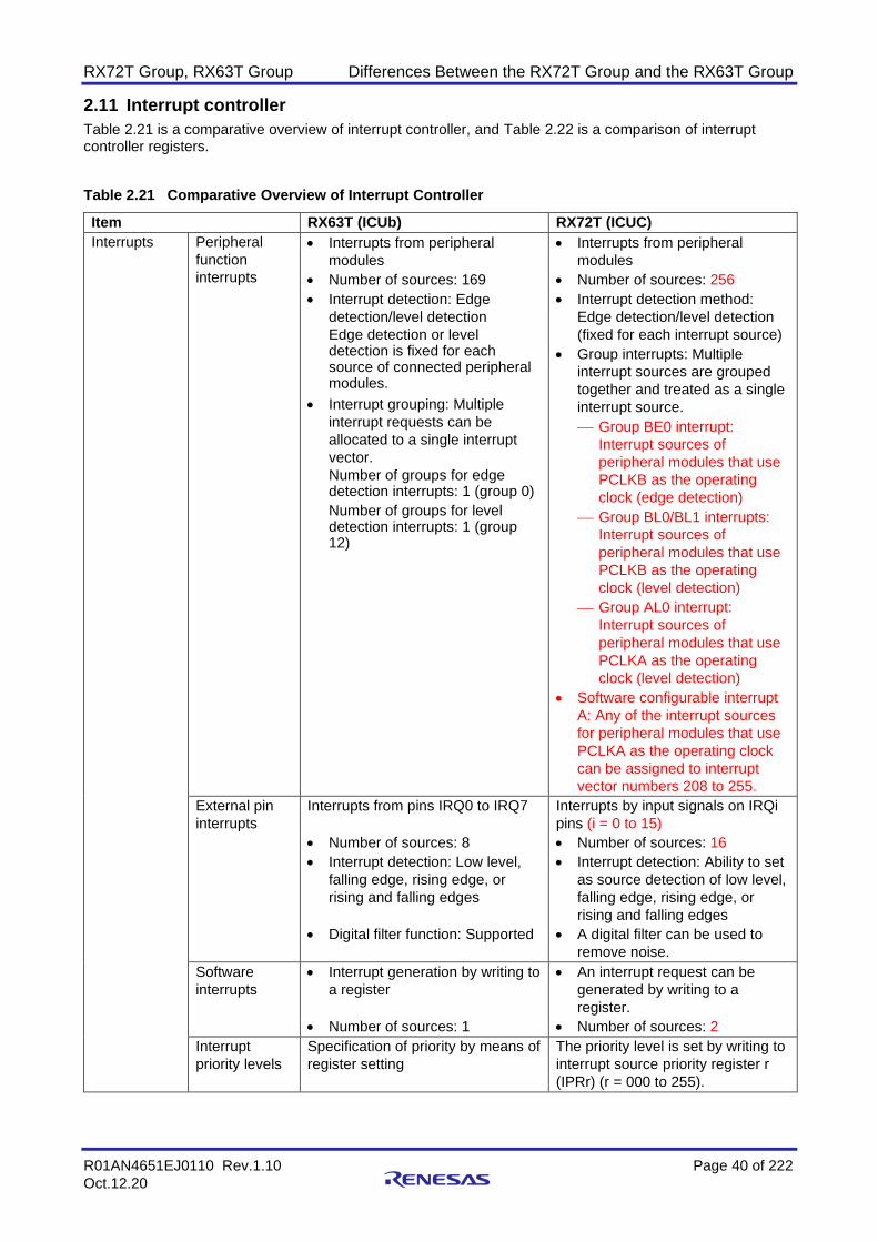
RX72T Group, RX63T Group Differences Between the RX72T Group and the RX63T Group
R01AN4651EJ0110 Rev.1.10 Page 40 of 222
Oct.12.20
2.11 Interrupt controller
Table 2.21 is a comparative overview of interrupt controller, and Table 2.22 is a comparison of interrupt controller registers.
Table 2.21 Comparative Overview of Interrupt Controller
Item RX63T (ICUb) RX72T (ICUC)
Interrupts Peripheral
function
interrupts
• Interrupts from peripheral
modules
• Number of sources: 169
• Interrupt detection: Edge
detection/level detection
Edge detection or level detection is fixed for each source of connected peripheral modules.
• Interrupt grouping: Multiple
interrupt requests can be
allocated to a single interrupt
vector.
Number of groups for edge detection interrupts: 1 (group 0)
Number of groups for level detection interrupts: 1 (group 12)
• Interrupts from peripheral
modules
• Number of sources: 256
• Interrupt detection method:
Edge detection/level detection
(fixed for each interrupt source)
• Group interrupts: Multiple
interrupt sources are grouped
together and treated as a single
interrupt source.
⎯ Group BE0 interrupt:
Interrupt sources of
peripheral modules that use
PCLKB as the operating
clock (edge detection)
⎯ Group BL0/BL1 interrupts:
Interrupt sources of
peripheral modules that use
PCLKB as the operating
clock (level detection)
⎯ Group AL0 interrupt:
Interrupt sources of
peripheral modules that use
PCLKA as the operating
clock (level detection)
• Software configurable interrupt
A: Any of the interrupt sources
for peripheral modules that use
PCLKA as the operating clock
can be assigned to interrupt
vector numbers 208 to 255.
External pin
interrupts
Interrupts from pins IRQ0 to IRQ7
• Number of sources: 8
• Interrupt detection: Low level,
falling edge, rising edge, or
rising and falling edges
• Digital filter function: Supported
Interrupts by input signals on IRQi
pins (i = 0 to 15)
• Number of sources: 16
• Interrupt detection: Ability to set
as source detection of low level,
falling edge, rising edge, or
rising and falling edges
• A digital filter can be used to
remove noise.
Software
interrupts
• Interrupt generation by writing to
a register
• Number of sources: 1
• An interrupt request can be
generated by writing to a
register.
• Number of sources: 2
Interrupt
priority levels
Specification of priority by means of
register setting
The priority level is set by writing to
interrupt source priority register r
(IPRr) (r = 000 to 255).

RX72T Group, RX63T Group Differences Between the RX72T Group and the RX63T Group
R01AN4651EJ0110 Rev.1.10 Page 41 of 222
Oct.12.20
Item RX63T (ICUb) RX72T (ICUC)
Interrupts Fast interrupt
function
Faster CPU interrupt processing
can be specified for a single
interrupt source only.
The CPU’s interrupt response time
can be reduced. This setting can be
used for one interrupt source only.
DTC control • An interrupt source can be used
to start the DTC.
• Number of DTC activating
sources: 124 (115 peripheral
function interrupts + 8 external
pin interrupts + 1 software
interrupt)
• An interrupt source can be used
to start the DTC.
• Number of DTC activating
sources: 129 (111 peripheral
function interrupts + 16 external
pin interrupts + 2 software
interrupts)
DMAC control • An interrupt source can be used
to start the DMAC.
• Number of DMAC activating
sources: 119 (111 peripheral
function interrupts + 8 external
pin interrupts)
• An interrupt source can be used
to start the DMAC.
• Number of DMAC activating
sources: 107 (91 peripheral
function interrupts + 16 external
pin interrupts)
Non-
maskable
interrupts
NMI pin
interrupt
Interrupt from the NMI pin
• Interrupt detection: Falling
edge/rising edge
• Digital filter function: Supported
Interrupt by the input signal on the
NMI pin
• Interrupt detection: Falling edge
or rising edge
• Digital filter can be used to
remove noise.
Voltage
monitoring 1
interrupt
Voltage monitoring interrupt of
voltage detection circuit 1 (LVD1)
Interrupt from voltage detection
circuit 1 (LVD1)
Voltage
monitoring 2
interrupt
Voltage monitoring interrupt of
voltage detection circuit 2 (LVD2)
Interrupt from voltage detection
circuit 2 (LVD2)
Oscillation
stop detection
interrupt
Interrupt on detection of oscillation
having stopped
Interrupt occurs at detection of
main clock oscillation having
stopped.
WDT
underflow/
refresh error
interrupt
Interrupt at underflow of the down-
counter or occurrence of a refresh
error
Interrupt occurs when the watchdog
timer underflows or a refresh error
occurs.
IWDT underflow/ refresh error interrupt
Interrupt at underflow of the down-
counter or occurrence of a refresh
error
Interrupt occurs when the
independent watchdog timer
underflows or a refresh error
occurs.
RAM error
interrupt
⎯ Interrupt occurs when a parity
check error is detected in the RAM
or an ECC error is detected in the
ECCRAM.

RX72T Group, RX63T Group Differences Between the RX72T Group and the RX63T Group
R01AN4651EJ0110 Rev.1.10 Page 42 of 222
Oct.12.20
Item RX63T (ICUb) RX72T (ICUC)
Return from
low power
consumption
state
Sleep mode Exit sleep mode by non-maskable
interrupt, any interrupt source.
Exit sleep mode by any interrupt
source.
All-module
clock stop
mode
Exit all-module clock stop mode by
NMI pin interrupt, external pin
interrupt, or peripheral function
interrupt (voltage monitoring 1,
voltage monitoring 2, oscillation
stop detection interrupt, USB
resume, or IWDT).
Exit all-module clock stop mode by
NMI pin interrupt, external pin
interrupt, or peripheral function
interrupt (voltage monitoring 1,
voltage monitoring 2, oscillation
stop detection interrupt, USB
resume, IWDT, or TMR0 to TMR3).
Software
standby mode
Exit software standby mode by NMI
pin interrupt, external pin interrupt,
or peripheral function interrupt
(voltage monitoring 1, voltage
monitoring 2, USB resume, or
IWDT).
Exit software standby mode by NMI
pin interrupt, external pin interrupt,
or peripheral function interrupt
(voltage monitoring 1, voltage
monitoring 2, USB resume, or
IWDT).
Deep software
standby mode
Exit deep software standby mode
by NMI pin interrupt, any of certain
external pin interrupts, or peripheral
function interrupt (voltage
monitoring 1 or voltage monitoring
2).
Exit deep software standby mode
by NMI pin interrupt, any of certain
external pin interrupts, or peripheral
function interrupt (voltage
monitoring 1 or voltage monitoring
2).
Table 2.22 Comparison of Interrupt Controller Registers
Register Bit RX63T (ICUb) RX72T (ICUC)
IRn*1 ⎯ Interrupt request register n
(n = 016 to 252)
Interrupt request register n
(n = 016 to 255)
IPRn*1 ⎯ Interrupt source priority register n
(n = 000 to 250)
Interrupt source priority register n
(n = 000 to 255)
SWINT2R ⎯ ⎯ Software interrupt 2 generation
register
DTCERn*1 ⎯ DTC activation enable register n
(n = 027 to 251)
DTC transfer request enable
register n (n = 026 to 255)
DMRSRm ⎯ DMAC activation request select
register m
(m = 0 to 3)
DMAC trigger select register m
(m = 0 to 7)
IRQCRi ⎯ IRQ control register i
(i = 0 to 7)
IRQ control register i
(i = 0 to 15)
IRQFLTE1 ⎯ ⎯ IRQ pin digital filter enable
register 1
IRQFLTC1 ⎯ ⎯ IRQ pin digital filter setting
register 1
NMISR RAMST ⎯ RAM error interrupt status flag
NMIER RAMEN ⎯ RAM error interrupt enable bit
GRPm ⎯ Group m interrupt source register
(m = 00 or 12)
⎯
GRPBE0, GRPBL0/
GRPBL1, GRPAL0
⎯ ⎯ Group BE0, BL0/BL1, and AL0
interrupt request registers
GENm ⎯ Group m interrupt enable register
(m = 00 or 12)
⎯
GENBE0, GENBL0/
GENBL1, GENAL0
⎯ ⎯ Group BE0, BL0/BL1, and AL0
interrupt request enable registers
GCRm ⎯ Group m interrupt clear register
(m = 00)
⎯
GCRBE0 ⎯ ⎯ Group BE0 interrupt clear register

RX72T Group, RX63T Group Differences Between the RX72T Group and the RX63T Group
R01AN4651EJ0110 Rev.1.10 Page 43 of 222
Oct.12.20
Register Bit RX63T (ICUb) RX72T (ICUC)
PIARk ⎯ ⎯ Software configurable interrupt A
request register k
(k = 0h to 12h)
SLIARn ⎯ ⎯ Software configurable interrupt A
source select register n
(n = 208 to 255)
SLIPRCR ⎯ ⎯ Software configurable interrupt
source select register write
protect register
Note: 1. On the RX63T Group n = 253 to 255 correspond to a reserved area.

RX72T Group, RX63T Group Differences Between the RX72T Group and the RX63T Group
R01AN4651EJ0110 Rev.1.10 Page 44 of 222
Oct.12.20
2.12 Buses
Table 2.23 is a comparative overview of bus, Table 2.24 is a comparative overview of external bus, and Table 2.25 is a comparison of bus registers.
Table 2.23 Comparative Overview of Bus
Item RX63T RX72T
CPU buses Instruction
bus
• Connected to the CPU (for
instructions)
• Connected to on-chip memory
(RAM, ROM)
• Operates in synchronization with
the system clock (ICLK)
• Connected to the CPU (for
instructions)
• Connected to on-chip memory
(RAM, code flash memory)
• Operates in synchronization with
the system clock (ICLK)
Operand
bus
• Connected to the CPU (for
operands)
• Connected to on-chip memory
(RAM, ROM)
• Operates in synchronization with
the system clock (ICLK)
• Connected to the CPU (for
operands)
• Connected to on-chip memory
(RAM, code flash memory)
• Operates in synchronization with
the system clock (ICLK)
Memory
buses
Memory bus
1
Connected to RAM Connected to RAM
Memory bus
2
Connected to ROM Connected to code flash memory
Memory bus
3
― Connected to ECCRAM
Internal
main
buses
Internal
main bus 1 • Connected to the CPU
• Operates in synchronization with
the system clock (ICLK)
• Connected to the CPU
• Operates in synchronization with
the system clock (ICLK)
Internal
main bus 2 • Connected to the DMAC and DTC
• Connected to on-chip memory
(RAM, ROM)
• Operates in synchronization with
the system clock (ICLK)
• Connected to the DMAC and DTC
• Connected to on-chip memory
(RAM, code flash memory)
• Operates in synchronization with
the system clock (ICLK)
Internal
peripheral
buses
Internal
peripheral
bus 1
• Connected to peripheral modules
(DTC, DMAC, interrupt controller,
and bus error monitoring section)
• Operates in synchronization with
the system clock (ICLK)
• Connected to peripheral modules
(TFU, DTC, DMAC, interrupt
controller, and bus error
monitoring section)
• Operates in synchronization with
the system clock (ICLK)
Internal
peripheral
bus 2
• Connected to peripheral modules
(modules other than those
connected to internal peripheral
buses 1, 3, 4, and 5)
• Operates in synchronization with
the peripheral-module clock
(PCLKB)
• Connected to peripheral modules
(modules other than those
connected to internal peripheral
buses 1, 3, 4, and 5)
• Operates in synchronization with
the peripheral-module clock
(PCLKB)
Internal
peripheral
bus 3
• Connected to peripheral modules
(USB)
• Operates in synchronization with
the peripheral-module clock
(PCLKB)
• Connected to peripheral modules
(USBb and CMPC)
• Operates in synchronization with
the peripheral-module clock
(PCLKB)

RX72T Group, RX63T Group Differences Between the RX72T Group and the RX63T Group
R01AN4651EJ0110 Rev.1.10 Page 45 of 222
Oct.12.20
Item RX63T RX72T
Internal
peripheral
buses
Internal
peripheral
bus 4
• Connected to peripheral modules
(MTU3, GPT, and DPC)
• Operates in synchronization with
the peripheral-module clock
(PCLKA)
• Connected to peripheral modules
(MTU3, GPTW, HRPWM, RSPI,
and SCIi)
• Operates in synchronization with
the peripheral-module clock
(PCLKA)
Internal
peripheral
bus 5
Reserved area Reserved area
Internal
peripheral
bus 6
• Connected to ROM (P/E) and E2
DataFlash memory
• Operates in synchronization with
the FlashIF clock (FCLK)
• Connected to code flash (in P/E)
and data flash memory
• Operates in synchronization with
the FlashIF clock (FCLK)
External
bus
CS area • Connected to external devices
• Operates in synchronization with
the external-bus clock (BCLK:
50 MHz (max.))
• Connected to external devices
• Operates in synchronization with
the external-bus clock (BCLK:
40 MHz (max.))

RX72T Group, RX63T Group Differences Between the RX72T Group and the RX63T Group
R01AN4651EJ0110 Rev.1.10 Page 46 of 222
Oct.12.20
Table 2.24 Comparative Overview of External Bus
Item RX63T RX72T
External address space • The external address space is
divided into four CS areas (CS0:
1 MB, CS1: 1 MB, CS2: 1 MB,
CS3: 1 MB) for management.
• Chip select signals can be output
for each area.
• Bus width can be set for each
area.
⎯ Separate bus: An 8 or 16-bit
bus space is selectable.
⎯ Address/data multiplexed bus:
An 8 or 16-bit bus space is
selectable.
• The endian mode can be specified
for each area.
• The external address space is
divided into four CS areas (CS0:
2 MB, CS1: 2 MB, CS2: 2 MB,
CS3: 2 MB) for management.
• Chip select signals can be output
for each area.
• Bus width can be set for each
area.
⎯ Separate bus: An 8 or 16-bit
bus space is selectable.
⎯ Address/data multiplexed bus:
An 8 or 16-bit bus space is
selectable.
• The endian mode can be specified
for each area.
CS area controller • Recovery cycles can be inserted.
⎯ Read recovery: Up to 15
cycles
⎯ Write recovery: Up to 15 cycles
• Cycle wait function: Wait for up to
31 cycles (page access: up to 7
cycles)
• Wait control can be used to
specify the following:
⎯ Timing of assertion and
negation for chip-select signals
(CS0# to CS3#)
⎯ Timing of assertion of the read
signal (RD#) and write signals
(WR0#/WR# and WR1#)
⎯ Timing with which data output
starts and ends
• Write access mode: Single write
strobe mode/byte strobe mode
• Separate bus or address/data
multiplexed bus can be set for
each area.
• Recovery cycles can be inserted.
⎯ Read recovery: Up to 15
cycles
⎯ Write recovery: Up to 15 cycles
• Cycle wait function: Wait for up to
31 cycles (page access: up to 7
cycles)
• Wait control can be used to
specify the following:
⎯ Timing of assertion and
negation for chip-select signals
(CS0# to CS3#)
⎯ Timing of assertion of the read
signal (RD#) and write signals
(WR0#/WR# and WR1#)
⎯ Timing with which data output
starts and ends
• Write access mode: Single write
strobe mode/byte strobe mode
• Separate bus or address/data
multiplexed bus can be set for
each area.
Write buffer function When write data from the bus master
has been written to the write buffer,
write access by the bus master ends.
When write data from the bus master
has been written to the write buffer,
write access by the bus master ends.
Frequency The CS area controller (CSC)
operates in synchronization with the
external-bus clock (BCLK).
The CS area controller (CSC)
operates in synchronization with the
external-bus clock (BCLK).
Address buses A19 to A0 A20 to A0
Table 2.25 Comparison of Bus Registers
Register Bit RX63T RX72T
BUSPRI BPRA[1:0] Memory bus 1 (on-chip RAM) priority
control bits
Memory buses 1 and 3
(RAM/ECCRAM) priority control bits

RX72T Group, RX63T Group Differences Between the RX72T Group and the RX63T Group
R01AN4651EJ0110 Rev.1.10 Page 47 of 222
Oct.12.20
2.13 Memory-Protection Unit
Table 2.26 is a comparative overview of memory-protection unit, and Table 2.27 is a comparison of memory-protection unit registers.
Table 2.26 Comparative Overview of Memory-Protection Unit
Item RX63T (MPU) RX72T (MPU)
Region covered by
memory protection
and processor mode
0000 0000h to FFFF FFFFh (in user
mode)
No memory protection in supervisor
mode
0000 0000h to FFFF FFFFh (in user
mode)
No memory protection in supervisor
mode
Number of regions 8 8
Page size (smallest
unit of protection)
16 bytes 16 bytes
Specification of
addresses of
individual regions
Specification by start page number and
end page number
Specification by start page number and
end page number
Setting to enable
memory protection
for individual regions
Enabled for each region by the V (valid)
bit in the corresponding region-n end
page number register (REPAGEn)
(n = 0 to 7).
Enabled for each region by the V (valid)
bit in the corresponding region-n end
page number register (REPAGEn)
(n = 0 to 7).
Access-control
information settings
for individual regions
Instruction execution: Permission to
execute
Operand access: Permission to read,
permission to write
Instruction execution: Permission to
execute
Operand access: Permission to read,
permission to write
Start of memory-
protection operation
After the memory-protection function
has been enabled, access monitoring
starts at the transition to user mode.
After the memory-protection function
has been enabled, access monitoring
starts at the transition to user mode.
Memory-protection
error processing
At occurrence of access exception At occurrence of access exception
Addresses where
memory-protection
errors are generated
Instruction execution address: The PC
value is preserved on the stack.
Operand access address: The address
is stored in the data memory-protection
error address register (MPDEA).
Instruction execution address: The PC
value is preserved on the stack.
Operand access address: The address
is stored in the data memory-protection
error address register (MPDEA).
Determining sources
of memory-protection
errors
Sources are stored in the memory-
protection error status register
(MPESTS).
Sources are stored in the memory-
protection error status register
(MPESTS).
Background region
setting
Access-control information can be set
for the background region (the entire
address space).
Access-control information can be set
for the background region (the entire
address space).
Processing where
regions overlap
If there is overlap between regions at a
given address, and the access-control
information of the regions differ,
permission is given priority.
If there is overlap between regions at a
given address, and the access-control
information of the regions differ,
permission is given priority.
Transition to user
mode
After updating the registers related to
the memory-protection unit, be sure to
read the registers that were last written
to and check that the settings have
taken effect before transitioning to user
mode.
After updating the registers related to
the memory-protection unit, be sure to
read one of the registers that were last
written to and check that the settings
have taken effect before transitioning to
user mode.

RX72T Group, RX63T Group Differences Between the RX72T Group and the RX63T Group
R01AN4651EJ0110 Rev.1.10 Page 48 of 222
Oct.12.20
Table 2.27 Comparison of Memory-Protection Unit Registers
Register Bit RX63T (MPU) RX72T (MPU)
MPESTS IA (RX63T)
IMPER (RX72T)
Instruction memory-protection
error generated bit
Instruction memory-protection
error generated bit
DA (RX63T)
DMPER (RX72T)
Data memory-protection error
generation bit
Data memory-protection error
generation bit

RX72T Group, RX63T Group Differences Between the RX72T Group and the RX63T Group
R01AN4651EJ0110 Rev.1.10 Page 49 of 222
Oct.12.20
2.14 DMA Controller
Table 2.28 is a comparative overview of DMA controller, and Table 2.29 is a comparison of DMA controller registers.
Table 2.28 Comparative Overview of DMA Controller
Item RX63T (DMACA) RX72T (DMACAa)
Number of channels 4 channels (DMACm (m = 0 to 3)) 8 channels (DMACm (m = 0 to 7))
Transfer space 512 MB (within 00000000h to
0FFFFFFFh or F0000000h to
FFFFFFFFh, excluding reserved
areas)
512 MB (within 00000000h to
0FFFFFFFh or F0000000h to
FFFFFFFFh, excluding reserved
areas)
Max. transfer data count 1 million data units (maximum
transfer count in block transfer
mode: 1,024 data units 1,024
blocks)
64 million data units (maximum
transfer count in block transfer
mode: 1,024 data units 65,536
blocks)
DMAC activation source Ability to select activation source for
each channel
• Software trigger
• Interrupt requests from peripheral
module/trigger input on external
interrupt input pin
Ability to select activation source for
each channel
• Software trigger
• Interrupt requests from peripheral
module/trigger input on external
interrupt input pin
Channel priority Channel 0 > Channel 1 > Channel 2
> Channel 3
(Channel 0: Highest priority)
Channel 0 > Channel 1 > Channel 2
> Channel 3 ... > Channel 7
(Channel 0: Highest priority)
Transfer
data
Single data
unit
Bit length: 8, 16, or 32 bits Bit length: 8, 16, or 32 bits
Block size Data count: 1 to 1,024 data units Data count: 1 to 1,024 data units
Transfer
modes
Normal
transfer mode • One data transfer per DMA
transfer request
• Ability to specify mode in which
total number of data transfers is
not set (free running mode)
• One data transfer per DMA
transfer request
• Ability to specify mode in which
total number of data transfers is
not set (free running mode)
Repeat
transfer mode • One data transfer per DMA
transfer request
• Return to the transfer start
address on completion of data
transfer equal to repeat size
specified for transfer source or
destination.
• Max. settable repeat size: 1,024
• One data transfer per DMA
transfer request
• Return to the transfer start
address on completion of data
transfer equal to repeat size
specified for transfer source or
destination.
• Max. settable repeat size: 1,024
Block transfer
mode • One block data transfer per DMA
transfer request
• Max. settable block size:
1,024 data units
• One block data transfer per DMA
transfer request
• Max. settable block size:
1,024 data units
Selectable
function
Extended
repeat area
function
• Ability to repeat address values in
a specified range with the upper
bit values in the transfer address
register fixed
• Ability to specify extended repeat
area of 2 bytes to 128 MB for
transfer source and destination
separately
• Ability to repeat address values in
a specified range with the upper
bit values in the transfer address
register fixed
• Ability to specify extended repeat
area of 2 bytes to 128 MB for
transfer source and destination
separately

RX72T Group, RX63T Group Differences Between the RX72T Group and the RX63T Group
R01AN4651EJ0110 Rev.1.10 Page 50 of 222
Oct.12.20
Item RX63T (DMACA) RX72T (DMACAa)
Interrupt
requests
Transfer end
interrupt
Generated on completion of transfer
of data count specified by transfer
counter.
• Generated when the specified
number of transfers is completed
in normal transfer mode.
• Generated when the specified
repeat count of transfers is
completed in repeat transfer
mode.
• Generated when the specified
block count of transfers is
completed in block transfer
mode.
Transfer
escape end
interrupt
Generated on completion of data
transfer equal to repeat size or when
extended repeat area overflows.
Generated on completion of data
transfer equal to repeat size or when
extended repeat area overflows.
Event link function ⎯ An event link request is generated
after each data transfer (for block
transfer, after each block is
transferred).
Low power consumption
function
Ability to specify transition to module
stop state
Ability to specify transition to module
stop state
Table 2.29 Comparison of DMA Controller Registers
Register Bit RX63T (DMACA) RX72T (DMACAa)
DMCRB ⎯ DMA block transfer count register
(b9 to b0)
DMA block transfer count register
(b15 to b0)
DMIST ⎯ ⎯ DMAC74 interrupt status monitor
register
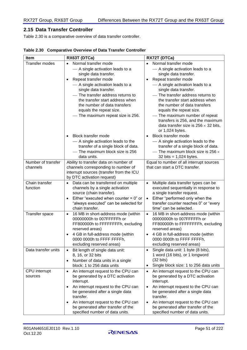
RX72T Group, RX63T Group Differences Between the RX72T Group and the RX63T Group
R01AN4651EJ0110 Rev.1.10 Page 51 of 222
Oct.12.20
2.15 Data Transfer Controller
Table 2.30 is a comparative overview of data transfer controller.
Table 2.30 Comparative Overview of Data Transfer Controller
Item RX63T (DTCa) RX72T (DTCa)
Transfer modes • Normal transfer mode
⎯ A single activation leads to a
single data transfer.
• Repeat transfer mode
⎯ A single activation leads to a
single data transfer.
⎯ The transfer address returns to
the transfer start address when
the number of data transfers
equals the repeat size.
⎯ The maximum repeat size is 256.
• Block transfer mode
⎯ A single activation leads to the
transfer of a single block of data.
⎯ The maximum block size is 256
data units.
• Normal transfer mode
⎯ A single activation leads to a
single data transfer.
• Repeat transfer mode
⎯ A single activation leads to a
single data transfer.
⎯ The transfer address returns to
the transfer start address when
the number of data transfers
equals the repeat size.
⎯ The maximum number of repeat
transfers is 256, and the maximum
data transfer size is 256 32 bits,
or 1,024 bytes.
• Block transfer mode
⎯ A single activation leads to the
transfer of a single block of data.
⎯ The maximum block size is 256
32 bits = 1,024 bytes.
Number of transfer
channels
Ability to transfer data on number of
channels corresponding to number of
interrupt sources (transfer from the ICU
by DTC activation request)
Equal to number of all interrupt sources
that can start a DTC transfer.
Chain transfer
function
• Data can be transferred on multiple
channels by a single activation
source (chain transfer).
• Either “executed when counter = 0” or
“always executed” can be selected for
chain transfer.
• Multiple data transfer types can be
executed sequentially in response to
a single transfer request.
• Either “performed only when the
transfer counter reaches 0” or “every
time” can be selected.
Transfer space • 16 MB in short-address mode (within
00000000h to 007FFFFFh or
FF800000h to FFFFFFFFh, excluding
reserved areas)
• 4 GB in full-address mode (within
0000 0000h to FFFF FFFFh,
excluding reserved areas)
• 16 MB in short-address mode (within
00000000h to 007FFFFFh or
FF800000h to FFFFFFFFh, excluding
reserved areas)
• 4 GB in full-address mode (within
0000 0000h to FFFF FFFFh,
excluding reserved areas)
Data transfer units • Bit length of single data unit:
8, 16, or 32 bits
• Number of data units in a single
block: 1 to 256 data units
• Single data unit: 1 byte (8 bits),
1 word (16 bits), or 1 longword
(32 bits)
• Single block size: 1 to 256 data units
CPU interrupt
sources • An interrupt request to the CPU can
be generated by a DTC activation
interrupt.
• An interrupt request to the CPU can
be generated after a single data
transfer.
• An interrupt request to the CPU can
be generated after transfer of the
specified number of data units.
• An interrupt request to the CPU can
be generated by a DTC activation
interrupt.
• An interrupt request to the CPU can
be generated after a single data
transfer.
• An interrupt request to the CPU can
be generated after transfer of the
specified number of data units.

RX72T Group, RX63T Group Differences Between the RX72T Group and the RX63T Group
R01AN4651EJ0110 Rev.1.10 Page 52 of 222
Oct.12.20
Item RX63T (DTCa) RX72T (DTCa)
Event link function ⎯ An event link request is generated after
each data transfer (for block transfer,
after each block is transferred).
Read skip Transfer information read skipping can
be specified.
Reading of the transfer information can
be skipped when the same transfer is
repeated.
Write-back skip When the transfer source address or
transfer destination address is fixed,
write-back skipping is supported.
Write-back of transferred data that is not
updated can be skipped when the
address of the transfer source or
destination is fixed.
Low power
consumption
function
Ability to specify transition to module
stop state
Ability to transition to module stop state

RX72T Group, RX63T Group Differences Between the RX72T Group and the RX63T Group
R01AN4651EJ0110 Rev.1.10 Page 53 of 222
Oct.12.20
2.16 I/O Ports
Table 2.31 to
Table 2.33 are comparative overviews of I/O ports for each package, Table 2.34 is a comparison of I/O port functions, and Table 2.35 is a comparison of I/O port registers.
Table 2.31 Comparative Overview of I/O Ports on 144-Pin Packages
Item RX63T (144-Pin)
RX72T (144-Pin)
(With PGA Pseudo-Differential Input and USB Pin)
PORT0 P00 to P05 P00, P01
PORT1 P10 to P14 P10 to P17
PORT2 P20 to P26 P20 to P27
PORT3 P30 to P35 P30 to P37
PORT4 P40 to P47 P40 to P47
PORT5 P50 to P57 P50 to P55
PORT6 P60 to P65 P60 to P65
PORT7 P70 to P76 P70 to P76
PORT8 P80 to P82 P80 to P82
PORT9 P90 to P96 P90 to P96
PORTA PA0 to PA6 PA0 to PA7
PORTB PB0 to PB7 PB0 to PB7
PORTC PC0 to PC5 PC0 to PC6
PORTD PD0 to PD7 PD0 to PD7
PORTE PE0 to PE5 PE0 to PE6
PORTF PF0 to PF4 PF0 to PF3
PORTG PG0 to PG6 PG0 to PG2
PORTH ⎯ PH0 to PH7
PORTK ⎯ PK0 to PK2
Table 2.32 Comparative Overview of I/O Ports on 100-Pin Packages
(RX72T: With PGA Pseudo-Differential Input)
Item RX63T (100-Pin)
RX72T (100-Pin)
With PGA Pseudo-Differential
Input and USB Pin
With PGA Pseudo-Differential
Input and Without USB Pin
PORT0 P00, P01 P00, P01 P00, P01
PORT1 P10, P11 P10, P11 P10, P11
PORT2 P20 to P24 P20 to P24, P27 P20 to P24, P27
PORT3 P30 to P33 P30 to P33, P36, P37 P30 to P33, P36, P37
PORT4 P40 to P47 P40 to P47 P40 to P47
PORT5 P50 to P55 P52 to P55 P52 to P55
PORT6 P60 to P65 P60 to P65 P60 to P65
PORT7 P70 to P76 P70 to P76 P70 to P76
PORT8 P80 to P82 P80 to P82 P80 to P82
PORT9 P90 to P96 P90 to P96 P90 to P96
PORTA PA0 to PA5 PA0 to PA5 PA0 to PA5
PORTB PB0 to PB7 PB0 to PB6 PB0 to PB7
PORTD PD0 to PD7 PD2 to PD7 PD0 to PD7
PORTE PE0 to PE5 PE0 to PE5 PE0 to PE5
PORTH ⎯ PH0, PH4 PH0, PH4

RX72T Group, RX63T Group Differences Between the RX72T Group and the RX63T Group
R01AN4651EJ0110 Rev.1.10 Page 54 of 222
Oct.12.20
Table 2.33 Comparative Overview of I/O Ports on 100-Pin Packages
(RX72T: Without PGA Pseudo-Differential Input)
Item RX63T (100-Pin)
RX72T (100-Pin)
(Without PGA Pseudo-Differential Input and USB Pin)
PORT0 P00, P01 P00, P01
PORT1 P10, P11 P10, P11
PORT2 P20 to P24 P20 to P24
PORT3 P30 to P33 P30 to P33, P36, P37
PORT4 P40 to P47 P40 to P47
PORT5 P50 to P55 P50 to P55
PORT6 P60 to P65 P60 to P65
PORT7 P70 to P76 P70 to P76
PORT8 P80 to P82 P80 to P82
PORT9 P90 to P96 P90 to P96
PORTA PA0 to PA5 PA0 to PA5
PORTB PB0 to PB7 PB0 to PB7
PORTD PD0 to PD7 PD0 to PD7
PORTE PE0 to PE5 PE0 to PE5
Table 2.34 Comparison of I/O Port Functions
Item Port Symbol
RX63T
RX72T
144-/120-/112-/100-Pin
Versions 64-/48-Pin Versions
Input pull-up PORT0 ⎯ ⎯ P00, P01
PORT1 ⎯ ⎯ P10 to P17
PORT2 ⎯ ⎯ P20 to P27
PORT3 ⎯ ⎯ P30 to P37
PORT4 ⎯ ⎯ P43, P47
PORT5 ⎯ ⎯ P50 to P55
PORT6 ⎯ ⎯ P60 to P65
PORT7 ⎯ ⎯ P70 to P76
PORT8 ⎯ ⎯ P80 to P82
PORT9 ⎯ ⎯ P90 to P96
PORTA ⎯ ⎯ PA0 to PA7
PORTB ⎯ ⎯ PB0 to PB7
PORTC ⎯ ⎯ PC0 to PC6
PORTD ⎯ ⎯ PD0 to PD7
PORTE ⎯ ⎯ PE0, PE1, PE3 to
PE6
PORTF ⎯ ⎯ PF0 to PF3
PORTG ⎯ ⎯ PG0 to PG2
PORTH ⎯ ⎯ PH1 to PH3, PH5 to
PH7
PORTK ⎯ ⎯ PK0 to PK2

RX72T Group, RX63T Group Differences Between the RX72T Group and the RX63T Group
R01AN4651EJ0110 Rev.1.10 Page 55 of 222
Oct.12.20
Item Port Symbol
RX63T
RX72T
144-/120-/112-/100-Pin
Versions 64-/48-Pin Versions
Open-drain
output
PORT0 P02, P03 ⎯ P00, P01
PORT1 ⎯ ⎯ P10 to P17
PORT2 P22, P23, P26 P24 P20 to P27
PORT3 P34, P35 P30 P30 to P37
PORT4 ⎯ ⎯ P43, P47
PORT5 ⎯ ⎯ P50 to P55
PORT6 ⎯ ⎯ P60 to P65
PORT7 ⎯ ⎯ P70 to P76
PORT8 P80, P81 ⎯ P80 to P82
PORT9 P95, P96 P93, P94 P90 to P96
PORTA PA1, PA2, PA4, PA5 ⎯ PA0 to PA7
PORTB PB1, PB2, PB5, PB6 PB1, PB2, PB5, PB6 PB0 to PB7
PORTC ⎯ ⎯ PC0 to PC6
PORTD PD3, PD5 PD3, PD5 PD0 to PD7
PORTE ⎯ ⎯ PE0, PE1, PE3 to
PE6
PORTF PF2, PF3 ⎯ PF0 to PF3
PORTG PG0, PG1, PG3, PG4 ⎯ PG0 to PG2
PORTH ⎯ ⎯ PH1 to PH3, PH5 to
PH7
PORTK ⎯ ⎯ PK0 to PK2
Driving ability
switching
PORT0 P00, P01, P05 ⎯ P00, P01
PORT1 P11, P12 ⎯ P10 to P17
PORT2 P20 to P26 ⎯ P20 to P27
PORT3 P30 to P33 ⎯ P30 to P37
PORT4 ― ⎯ P43, P47
PORT5 P52, P53 ⎯ P50 to P55
PORT6 P60 to P65 ⎯ P60 to P65
PORT7 P70 to P76 ⎯ P70 to P76
PORT8 P80, P81 ⎯ P80 to P82
PORT9 P90 to P96 ⎯ P90 to P96
PORTA PA0 to PA6 ⎯ PA0 to PA7
PORTB PB0, PB3 to PB7 ⎯ PB0 to PB7
PORTC ⎯ ⎯ PC0 to PC6
PORTD PD0 to PD2, PD6, PD7 ⎯ PD0 to PD7
PORTE PE0, PE1, PE3 to PE5 ⎯ PE0, PE1, PE3 to
PE6
PORTF PF2, PF4 ⎯ PF0 to PF3
PORTG PG6 ⎯ PG0 to PG2
PORTH ⎯ ⎯ PH1 to PH3, PH5 to
PH7
PORTK ⎯ ⎯ PK0 to PK2

RX72T Group, RX63T Group Differences Between the RX72T Group and the RX63T Group
R01AN4651EJ0110 Rev.1.10 Page 56 of 222
Oct.12.20
Item Port Symbol
RX63T
RX72T
144-/120-/112-/100-Pin
Versions 64-/48-Pin Versions
5 V tolerant PORT0 ⎯ P00, P01 ⎯
PORT1 ⎯ P10, P11 ⎯
PORT2 ⎯ P22 to P24 ⎯
PORT3 ⎯ P30 to P34 ⎯
PORT7 ⎯ P70 to P76 ⎯
PORT9 ⎯ P91 to P94 ⎯
PORTA ⎯ PA2 to PA5 ⎯
PORTB ⎯ PB0 to PB7 PB1, PB2
PORTC ⎯ ⎯ PC0
PORTD ⎯ PD3 to PD7 PD2
Table 2.35 Comparison of I/O Port Registers
Register Bit RX63T RX72T
PDR B0 to B7 Pm0 to Pm7 I/O select bits
(m = 0 to 3, 7 to 9, A, B, D to G)
Pm0 to Pm7 I/O select bits
(m = 0 to 9, A to H, K)
PODR B0 to B7 Pm0 to Pm7 output data store bits
(m = 0 to 3, 7 to 9, A, B, D to G)
Pm0 to Pm7 output data store bits
(m = 0 to 9, A to H, K)
PIDR B0 to B7 Pm0 to Pm7 bits
(m = 0 to 9, A to G)
Pm0 to Pm7 bits
(m = 0 to 9, A to H, K)
PMR B0 to B7 Pm0 to Pm7 pin mode control bits
(m = 0 to 3, 7 to 9, A, B, D to G)
Pm0 to Pm7 pin mode control bits
(m = 0 to 9, A to H, K)
ODR0 B0 Pm0 output type select bit
(m = 3, 8, G)
Pm0 output type select bit
(m = 0 to 9, A to H, K)
B2 Pm1 output type select bit
(m = 8, A, B, G)
Pm1 output type select bit
(m = 0 to 9, A to H, K)
B4 Pm2 output type select bit
(m = 0, 2, A, B, F)
Pm2 output type select bit
(m = 0 to 9, A to H, K)
B6 Pm3 output type select bit
(m = 0, 2, 9, D, F, G)
Pm3 output type select bit
(m = 0 to 9, A to H, K)
ODR1 B0 Pm4 output type select bit
(m = 2, 3, A, G)
Pm4 output type select bit
(m = 1 to 7, 9, A to E, H)
B2 Pm5 output type select bit
(m = 3, 9, A, B, D)
Pm5 output type select bit
(m = 1 to 7, 9, A to E, H)
B4 Pm6 output type select bit
(m = 2, 9, B)
Pm6 output type select bit
(m = 1 to 7, 9, A to E, H)
B6 ⎯ Pm7 output type select bit
(m = 1 to 7, 9, A to E, H)
PCR ⎯ ⎯ Pull-up resistor control register
DSCR ⎯ ⎯ Driving ability control register
DSCR1 ⎯ Driving ability control register 1 ⎯
DSCR2 B0 to B5 ⎯ Pm0 to Pm5 drive capacity control
bit 2
(m = 7 to 9, B, D)

RX72T Group, RX63T Group Differences Between the RX72T Group and the RX63T Group
R01AN4651EJ0110 Rev.1.10 Page 57 of 222
Oct.12.20
Register Bit RX63T RX72T
DSCR2 B6 RSPI pins (MISOn, SSLn0 to
SSLn3) driving ability control bit
MISOn: P22, PA5, PD1
SSLn0: P30, PA3, PD6
SSLn1: P31, PA2, PD7
SSLn2: P32, PA1, PE0
SSLn3: P33, PA0, PE1
(n = A or B)
Pm6 drive capacity control bit 2
(m = 7 to 9, B, D)
B7 RSPI pins (RSPCKn, MOSIn)
driving ability control bit
RSPCKn: P24, PA4, PD0
MOSIn: P23, PB0, PD2
(n = A or B)
⎯
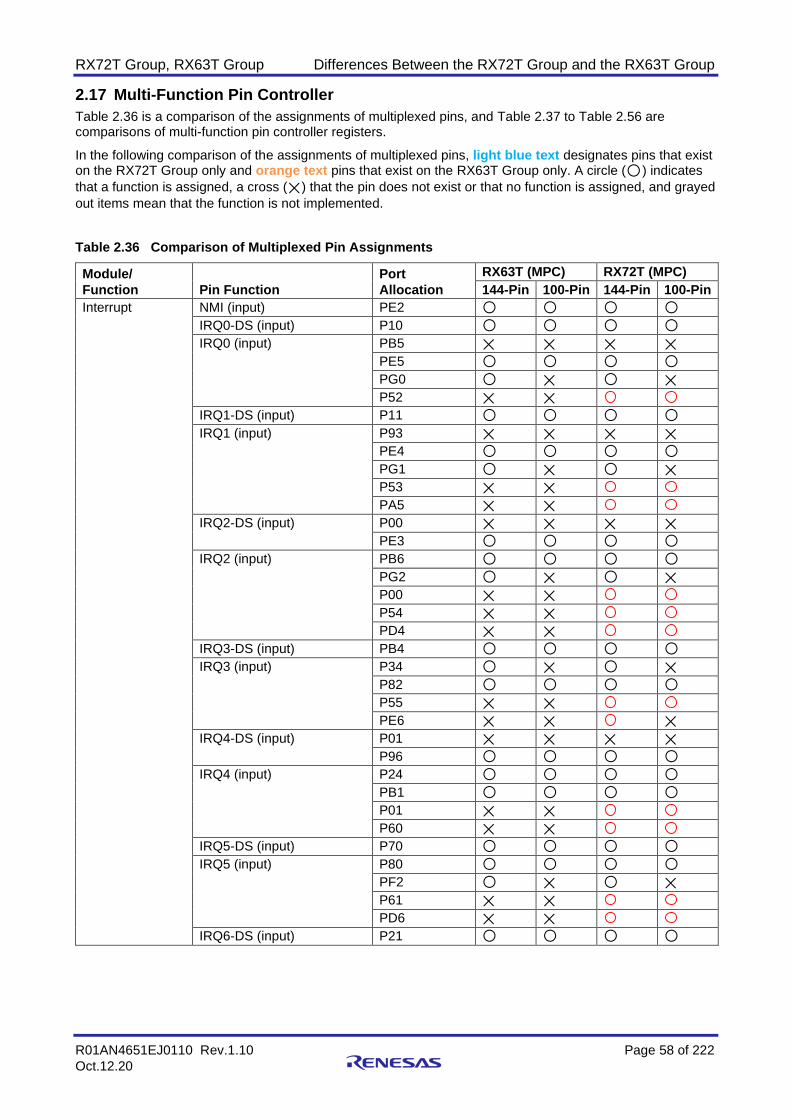
RX72T Group, RX63T Group Differences Between the RX72T Group and the RX63T Group
R01AN4651EJ0110 Rev.1.10 Page 58 of 222
Oct.12.20
2.17 Multi-Function Pin Controller
Table 2.36 is a comparison of the assignments of multiplexed pins, and Table 2.37 to Table 2.56 are comparisons of multi-function pin controller registers.
In the following comparison of the assignments of multiplexed pins, light blue text designates pins that exist on the RX72T Group only and orange text pins that exist on the RX63T Group only. A circle ( ) indicates
that a function is assigned, a cross ( ) that the pin does not exist or that no function is assigned, and grayed
out items mean that the function is not implemented.
Table 2.36 Comparison of Multiplexed Pin Assignments
Module/
Function Pin Function
Port
Allocation
RX63T (MPC) RX72T (MPC)
144-Pin 100-Pin 144-Pin 100-Pin
Interrupt NMI (input) PE2
IRQ0-DS (input) P10
IRQ0 (input) PB5
PE5
PG0
P52
IRQ1-DS (input) P11
IRQ1 (input) P93
PE4
PG1
P53
PA5
IRQ2-DS (input) P00
PE3
IRQ2 (input) PB6
PG2
P00
P54
PD4
IRQ3-DS (input) PB4
IRQ3 (input) P34
P82
P55
PE6
IRQ4-DS (input) P01
P96
IRQ4 (input) P24
PB1
P01
P60
IRQ5-DS (input) P70
IRQ5 (input) P80
PF2
P61
PD6
IRQ6-DS (input) P21

RX72T Group, RX63T Group Differences Between the RX72T Group and the RX63T Group
R01AN4651EJ0110 Rev.1.10 Page 59 of 222
Oct.12.20
Module/
Function Pin Function
Port
Allocation
RX63T (MPC) RX72T (MPC)
144-Pin 100-Pin 144-Pin 100-Pin
Interrupt IRQ6 (input) PD5
PG4
P31
P35
P62
IRQ7-DS (input) P20
IRQ7 (input) P03
PE0
P30
P63
PA6
IRQ8-DS (input) PK1 IRQ8 (input) P64
PB0
PD7
IRQ9-DS (input) PK2
IRQ9 (input) P12
P65
PB3
IRQ10-DS (input) PC5
IRQ10 (input) P13
P22
P25
IRQ11-DS (input) PC6
IRQ11 (input) P14
P23
P26
IRQ12-DS (input) P32
IRQ12 (input) P15 PC0
PF0
IRQ13-DS (input) P33
IRQ13 (input) P16
PC1
PF1
IRQ14-DS (input) PA1
IRQ14 (input) P17
PC3
PF3
IRQ15-DS (input) PK0
IRQ15 (input) P27 *1
PC2
PE1
Multi-function
timer unit 3
MTIOC0A (input/output) /
MTIOC0A# (input/output)
P31
PB3
MTIOC0B (input/output) /
MTIOC0B# (input/output)
P30
PB2
PC0

RX72T Group, RX63T Group Differences Between the RX72T Group and the RX63T Group
R01AN4651EJ0110 Rev.1.10 Page 60 of 222
Oct.12.20
Module/
Function Pin Function
Port
Allocation
RX63T (MPC) RX72T (MPC)
144-Pin 100-Pin 144-Pin 100-Pin
Multi-function
timer unit 3
MTIOC0C (input/output) /
MTIOC0C# (input/output)
P27 *1
PB1
PC1
MTIOC0D (input/output) /
MTIOC0D# (input/output)
PB0
PC2
MTIOC1A (input/output) /
MTIOC1A# (input/output)
P27 *1
PA5
PC6
MTIOC1B (input/output) /
MTIOC1B# (input/output)
PA4
PC5
MTIOC2A (input/output) /
MTIOC2A# (input/output)
P35
PA3
MTIOC2B (input/output) /
MTIOC2B# (input/output)
P34
PA2
MTIOC3A (input/output) /
MTIOC3A# (input/output)
P11
P33
MTIOC3B (input/output) /
MTIOC3B# (input/output)
P12
P71
MTIOC3C (input/output) /
MTIOC3C# (input/output)
P32
MTIOC3D (input/output) /
MTIOC3D# (input/output)
P15
P74
MTIOC4A (input/output) /
MTIOC4A# (input/output)
P13
P72
MTIOC4B (input/output) /
MTIOC4B# (input/output)
P14
P73
MTIOC4C (input/output) /
MTIOC4C# (input/output)
P16
P75
MTIOC4D (input/output) /
MTIOC4D# (input/output)
P17
P76
MTIC5U (input) /
MTIC5U# (input)
P24
P82
MTIC5V (input) /
MTIC5V# (input)
P23
P81
MTIC5W (input) /
MTIC5W# (input)
P22
P80
MTIOC6A (input/output) /
MTIOC6A# (input/output)
P33
PA1
MTIOC6B (input/output) /
MTIOC6B# (input/output)
P71
P95
MTIOC6C (input/output) /
MTIOC6C# (input/output)
P32
PA0
MTIOC6D (input/output) /
MTIOC6D# (input/output)
P74
P92
MTIOC7A (input/output) /
MTIOC7A# (input/output)
P72
MTIOC7A (input/output) /
MTIOC7A# (input/output)
P94

RX72T Group, RX63T Group Differences Between the RX72T Group and the RX63T Group
R01AN4651EJ0110 Rev.1.10 Page 61 of 222
Oct.12.20
Module/
Function Pin Function
Port
Allocation
RX63T (MPC) RX72T (MPC)
144-Pin 100-Pin 144-Pin 100-Pin
Multi-function
timer unit 3
MTIOC7B (input/output) /
MTIOC7B# (input/output)
P73
P93
MTIOC7C (input/output) /
MTIOC7C# (input/output)
P75
P91
MTIOC7D (input/output) /
MTIOC7D# (input/output)
P76
P90
MTIOC9A (input/output) /
MTIOC9A# (input/output)
P00
P21
P26
P35
PD7
MTIOC9B (input/output) P22
MTIOC9B (input/output) /
MTIOC9B# (input/output)
P10
P34
PC4
PE0
MTIOC9C (input/output) /
MTIOC9C# (input/output)
P01
P20
P25
PC6
PD6
MTIOC9D (input/output) P11
MTIOC9D (input/output) /
MTIOC9D# (input/output)
PC3
PC5
PE1
PE5
MTCLKA (input) /
MTCLKA# (input)
P21
P22
P33
PB3
PA7
MTCLKB (input) /
MTCLKB# (input)
P20
P23
P32
PB2
PA6
MTCLKC (input) /
MTCLKC# (input)
P11
P24
P31
PA7
PE4
MTCLKD (input) /
MTCLKD# (input)
P10
P22
P30
PA6
PE3
ADSM0 (output) PA7
PB2
PC2

RX72T Group, RX63T Group Differences Between the RX72T Group and the RX63T Group
R01AN4651EJ0110 Rev.1.10 Page 62 of 222
Oct.12.20
Module/
Function Pin Function
Port
Allocation
RX63T (MPC) RX72T (MPC)
144-Pin 100-Pin 144-Pin 100-Pin
Multi-function
timer unit 3
ADSM1 (output) PA6
PB1
PC1
Port output
enable 3
POE0# (input) P70
POE4# (input) P96
POE8# (input) PB4
POE9# (input) P11
P27 *1
POE10# (input) PE4
PE2
PE6
POE11# (input) PE3
PB5
POE12# (input) PG5
P01
P10
PK2
POE13# (input) PK1
POE14# (input) PK0
General PWM
timer
GTIOC0A (input/output) /
GTIOC0A# (input/output)
P12
P71
PD2
PD7
PG1
GTIOC0B (input/output) /
GTIOC0B# (input/output)
P15
P74
PD1 *4
PD6
PG2
GTIOC1A (input/output) /
GTIOC1A# (input/output)
P13
P72
PD0 *4
PD5
PK2
GTIOC1B (input/output) /
GTIOC1B# (input/output)
P16
P75
PB7 *4
PD4
PG0
GTIOC2A (input/output) /
GTIOC2A# (input/output)
P14
P73
PB6
PD3
PK0

RX72T Group, RX63T Group Differences Between the RX72T Group and the RX63T Group
R01AN4651EJ0110 Rev.1.10 Page 63 of 222
Oct.12.20
Module/
Function Pin Function
Port
Allocation
RX63T (MPC) RX72T (MPC)
144-Pin 100-Pin 144-Pin 100-Pin
General PWM
timer
GTIOC2B (input/output) /
GTIOC2B# (input/output)
P17
P76
PB5
PB6
PB7
PD2
PK1
GTIOC3A (input/output) /
GTIOC3A# (input/output)
P32
P00
PD1 *4
PD7
PE5
GTIOC3B (input/output) /
GTIOC3B# (input/output)
P11
P33
P01
PD0 *4
PD6
GTIOC4A (input/output) /
GTIOC4A# (input/output)
P71
P95
GTIOC4B (input/output) /
GTIOC4B# (input/output)
P74
P92
GTIOC5A (input/output) /
GTIOC5A# (input/output)
P72
P94
GTIOC5B (input/output) /
GTIOC5B# (input/output)
P75
P91
GTIOC6A (input/output) /
GTIOC6A# (input/output)
P73
P93
PG3
GTIOC6B (input/output) /
GTIOC6B# (input/output)
P76
P90
PG4
GTIOC7A (input/output) /
GTIOC7A# (input/output)
P12
P95
PG0
GTIOC7B (input/output) /
GTIOC7B# (input/output)
P15
P92
PG1
GTIOC8A (input/output) /
GTIOC8A# (input/output)
P13
P94
GTIOC8B (input/output) /
GTIOC8B# (input/output)
P16
P91
GTIOC9A (input/output) /
GTIOC9A# (input/output)
P14
P93
GTIOC9B (input/output) /
GTIOC9B# (input/output)
P17
P90
GTETRG/GTETRG0 PB4
GTETRG1 P34

RX72T Group, RX63T Group Differences Between the RX72T Group and the RX63T Group
R01AN4651EJ0110 Rev.1.10 Page 64 of 222
Oct.12.20
Module/
Function Pin Function
Port
Allocation
RX63T (MPC) RX72T (MPC)
144-Pin 100-Pin 144-Pin 100-Pin
General PWM
timer
GTETRGA (input) P01
P11
P70
P96
PB4
PD5
PE3
PE4
PE6
PF3
PG2
GTETRGB (input) P01
P10
P34
P70
P96
PB4
PD4
PE3
PE4
PE5
PE6
PF2
GTETRGC (input) P01
P11
P70
P96
PB4
PD3
PE3
PE4
PE6
PF1
GTETRGD (input) P01
P10
P70
P96
PB4
PE3
PE4
PE5
PE6
PF0
GTADSM0 (output) P35
PA3
PA7
PB2
PC2

RX72T Group, RX63T Group Differences Between the RX72T Group and the RX63T Group
R01AN4651EJ0110 Rev.1.10 Page 65 of 222
Oct.12.20
Module/
Function Pin Function
Port
Allocation
RX63T (MPC) RX72T (MPC)
144-Pin 100-Pin 144-Pin 100-Pin
General PWM
timer
GTADSM1 (output) P34
PA2
PA6
PB1
PC1
Serial
communications
interface
RXD0 (input) /
SMISO0 (input/output) /
SSCL0 (input/output)
P22
PA5
PB1
TXD0 (output) /
SMOSI0 (input/output) /
SSDA0 (input/output)
P23
PA4
PB2
SCK0 (input/output) P23
P30
PA3
PB3
CTS0# (input) /
RTS0# (output) /
SS0# (input)
P00
P01
P22
P24
PD7
RXD1 (input) /
SMISO1 (input/output) /
SSCL1 (input/output)
P93
P96
PD5
PF2
P34
PC3
TXD1 (output) /
SMOSI1 (input/output) /
SSDA1 (input/output)
P26
P94
P95
PD3
PF3
P35
PC4
SCK1 (input/output) P25
P92
PD4
PG6
CTS1# (input) /
RTS1# (output) /
SS1# (input)
P70
P91
P94
P26
PD6
RXD2 (input) /
SMISO2 (input/output) /
SSCL2 (input/output)
P03
PA2
PG1
TXD2 (output) /
SMOSI2 (input/output) /
SSDA2 (input/output)
P02
PA1
PG0

RX72T Group, RX63T Group Differences Between the RX72T Group and the RX63T Group
R01AN4651EJ0110 Rev.1.10 Page 66 of 222
Oct.12.20
Module/
Function Pin Function
Port
Allocation
RX63T (MPC) RX72T (MPC)
144-Pin 100-Pin 144-Pin 100-Pin
Serial
communications
interface
SCK2 (input/output) P14
PA0
PG2
CTS2# (input) /
RTS2# (output) /
SS2# (input)
P13
P93
RXD3 (input) /
SMISO3 (input/output) /
SSCL3 (input/output)
P34
PG4
TXD3 (output) /
SMOSI3 (input/output) /
SSDA3 (input/output)
P35
PG3
SCK3 (input/output) PG5
CTS3# (input) /
RTS3# (output) /
SS3# (input)
PA6
RXD5 (input) /
SMISO5 (input/output) /
SSCL5 (input/output)
PB6
PE0
PK0
TXD5 (output) /
SMOSI5 (input/output) /
SSDA5 (input/output)
PB5
PD7
PK1
SCK5 (input/output) PB7 *4
PD2
PK2
CTS5# (input) /
RTS5# (output) /
SS5# (input)
PB4
PE1
RXD6 (input) /
SMISO6 (input/output) /
SSCL6 (input/output)
P80
PA5
PB1
TXD6 (output) /
SMOSI6 (input/output) /
SSDA6 (input/output)
P81
PB0
PB2
SCK6 (input/output) P82
PA4
PB3
CTS6# (input) /
RTS6# (output) /
SS6# (input)
P10
PA2
RXD8 (input) /
SMISO8 (input/output) /
SSCL8 (input/output)
P22
PA5
PC0
PD1 *4
TXD8 (output) /
SMOSI8 (input/output) /
SSDA8 (input/output)
P21
P23
PA4
PC1
PD0 *4

RX72T Group, RX63T Group Differences Between the RX72T Group and the RX63T Group
R01AN4651EJ0110 Rev.1.10 Page 67 of 222
Oct.12.20
Module/
Function Pin Function
Port
Allocation
RX63T (MPC) RX72T (MPC)
144-Pin 100-Pin 144-Pin 100-Pin
Serial
communications
interface
SCK8 (input/output) P20
P24
P30
PA3
PC2
PD2
CTS8# (input) /
RTS8# (output) /
SS8# (input)
P20
P24
P30
P35
P96
PK1
RXD9 (input) /
SMISO9 (input/output) /
SSCL9 (input/output)
P00
PA2
PG0
TXD9 (output) /
SMOSI9 (input/output) /
SSDA9 (input/output)
P01
PA1
PA3
PG1
SCK9 (input/output) PA0
PE4
PE5
PG2
CTS9# (input) /
RTS9# (output) /
SS9# (input)
P34
P70
PE3
PE5
PK2
RXD11 (input) /
SMISO11 (input/output) /
SSCL11 (input/output)
PA1
PA7
PB6
PC6
PD5
PF1
TXD11 (output) /
SMOSI11 (input/output) /
SSDA11 (input/output)
PA0
PA6
PB5
PC5
PD3
PF0
SCK11 (input/output) PA2
PB4
PB7 *4
PD4
PF2
CTS11# (input) /
RTS11# (output) /
SS11# (input)
PB0
PB4
PD6
PF3

RX72T Group, RX63T Group Differences Between the RX72T Group and the RX63T Group
R01AN4651EJ0110 Rev.1.10 Page 68 of 222
Oct.12.20
Module/
Function Pin Function
Port
Allocation
RX63T (MPC) RX72T (MPC)
144-Pin 100-Pin 144-Pin 100-Pin
Serial
communications
interface
RXD12 (input) /
SMISO12 (input/output) /
SSCL12 (input/output) /
RXDX12 (input)
P80
PB6
P00
P22
PA7
PC3
TXD12 (output) /
SMOSI12 (input/output) /
SSDA12 (input/output) /
TXDX12 (output) /
SIOX12 (input/output)
P81
PB5
P01
P21
P23
PA6
PC4
SCK12 (input/output) P82
PB7 *4
CTS12# (input) /
RTS12# (output) /
SS12# (input)
PB4
PE1
I2C bus interface SCL0 (input/output) /
SCL (input/output)
PB1
SDA0 (input/output) /
SDA (input/output)
PB2
SCL1 (input/output) P25
SDA1 (input/output) P26
USB 2.0 FS
Host/Function
module
USB0_DPUPE ⎯
USB0_VBUSEN (output) P13
PA0 *3
PC1
PB5 *3
USB0_OVRCURA (input) PE1
PA1 *3
PB6 *3
PC2
USB0_VBUS (input) PE5
PC0
PD2 *3
USB0_EXICEN (output) PD1
PA0 *3
PC1
USB0_OVRCURB (input) PE0 *3
P34
PB4 *3
PB7
USB0_ID (input) PD2
PA1 *3
PC2
USB0_DRPD (output) P01
USB0_DPRPD (output) P12

RX72T Group, RX63T Group Differences Between the RX72T Group and the RX63T Group
R01AN4651EJ0110 Rev.1.10 Page 69 of 222
Oct.12.20
Module/
Function Pin Function
Port
Allocation
RX63T (MPC) RX72T (MPC)
144-Pin 100-Pin 144-Pin 100-Pin
CAN module CRX1 (input) /
CRX0 (input)
PE0
P22
PB6
PA1
PA7
PC6
PF3
CTX1 (output) /
CTX0 (output)
P23
PB5
PD7
PA0
PA6
PC5
PF2
Serial peripheral
interface
RSPCKA (input/output) P24
PA4
PD0 *4
P20
PB3
MOSIA (input/output) P23
PB0
PD2
P21
MISOA (input/output) P22
PA5
PD1 *4
SSLA0 (input/output) P30
PA3
PD6
SSLA1 (output) P31
PA2
PD7
SSLA2 (output) P32
PA1
PE0
SSLA3 (output) P33
PA0
PE1
RSPCKB (input/output) P24
PA4
PD0
MOSIB (input/output) P23
PB0
PD2
MISOB (input/output) P22
PA5
PD1
SSLB0 (input/output) P30
PA3
PD6

RX72T Group, RX63T Group Differences Between the RX72T Group and the RX63T Group
R01AN4651EJ0110 Rev.1.10 Page 70 of 222
Oct.12.20
Module/
Function Pin Function
Port
Allocation
RX63T (MPC) RX72T (MPC)
144-Pin 100-Pin 144-Pin 100-Pin
Serial peripheral
interface
SSLB1 (output) P31
PA2
PD7
SSLB2 (output) P32
PA1
PE0
SSLB3 (output) P33
PA0
PE1
12-bit A/D
converter
AN000 (input)*5 P40
AN001 (input)*5 P41
AN002 (input)*5 P42
AN003 (input)*5 P43
AN004 (input)*5 P44
PH1
AN005 (input)*5 P45
PH2
AN006 (input)*5 P46
PH3
AN007 (input)*5 P47
PH0 *1
ADTRG0# (input) P20
PA4
PA1
ADST0 (output) P26
PD6
PE5
PGAVSS0 (input)*5 PH0 *1
AN100 (input)*5 P44
AN101 (input)*5 P45
AN102 (input)*5 P46
AN103 (input)*5 P47
AN104 (input)*5 PH5
AN105 (input)*5 PH6
AN106 (input)*5 PH7
AN107 (input)*5 PH4 *1
ADTRG1# (input) P21
PA5
ADST1 (output) P00
P25
PGAVSS1 (input)*5 PH4 *1
AN200 (input)*5 P52
AN201 (input)*5 P53
AN202 (input)*5 P54
AN203 (input)*5 P55
AN204 (input)*5 P50 *2
AN205 (input)*5 P51 *2
AN206 (input)*5 P60
AN207 (input)*5 P61
AN208 (input)*5 P62

RX72T Group, RX63T Group Differences Between the RX72T Group and the RX63T Group
R01AN4651EJ0110 Rev.1.10 Page 71 of 222
Oct.12.20
Module/
Function Pin Function
Port
Allocation
RX63T (MPC) RX72T (MPC)
144-Pin 100-Pin 144-Pin 100-Pin
12-bit A/D
converter
AN209 (input)*5 P63
AN210 (input)*5 P64
AN211 (input)*5 P65
AN216 (input)*5 P20
AN217 (input)*5 P21
ADTRG2# (input) P22
PB0
ADST2 (output) P01
PC4
10-bit A/D
converter
AN0 (input) P60
AN1 (input) P61
AN2 (input) P62
AN3 (input) P63
AN4 (input) P64
AN5 (input) P65
AN6 (input) P50
AN7 (input) P51
AN8 (input) P52
AN9 (input) P53
AN10 (input) P54
AN11 (input) P55
AN12 (input) P56
AN13 (input) P57
AN14 (input) PC0
AN15 (input) PC1
AN16 (input) PC2
AN17 (input) PC3
AN18 (input) PC4
AN19 (input) PC5
ADTRG# (input) P22
PG5
D/A converter DA0 (output)*5 P54
P64
DA1 (output)*5 P55
P65
Clock frequency
accuracy
measurement
circuit
CACREF (input) P00
P01
P23
PB3
8-bit timer TMO0 (output) P33
P35
PB0
PD3
TMCI0 (input) PB1
PD4
TMRI0 (input) PB2
PD5
TMO1 (output) PD6
PF0

RX72T Group, RX63T Group Differences Between the RX72T Group and the RX63T Group
R01AN4651EJ0110 Rev.1.10 Page 72 of 222
Oct.12.20
Module/
Function Pin Function
Port
Allocation
RX63T (MPC) RX72T (MPC)
144-Pin 100-Pin 144-Pin 100-Pin
8-bit timer TMCI1 (input) PD2
PE0
TMRI1 (input) PD7
TMO2 (output) P23
PA0
PA7
PD1 *4
TMCI2 (input) P24
TMRI2 (input) P22
TMO3 (output) P11
PF2
TMCI3 (input) PA5
TMRI3 (input) P10
TMO4 (output) P22
P34
P82
PA1
PD2
TMCI4 (input) P21
P81
TMRI4 (input) P20
P80
TMO5 (output) PE1
PF1
TMCI5 (input) PE0
TMRI5 (input) PD7
TMO6 (output) P24
P32
PA6
PD0 *4
TMCI6 (input) P30
PD4
TMRI6 (input) P31
PD5
TMO7 (output) PA2
PF3
TMCI7 (input) PA4
TMRI7 (input) PA3
Comparator COMP0 (output) P00
P24
PF3
PG2
COMP1 (output) P01
P23
PF2
PG1
COMP2 (output) P22
PF1
PG0

RX72T Group, RX63T Group Differences Between the RX72T Group and the RX63T Group
R01AN4651EJ0110 Rev.1.10 Page 73 of 222
Oct.12.20
Module/
Function Pin Function
Port
Allocation
RX63T (MPC) RX72T (MPC)
144-Pin 100-Pin 144-Pin 100-Pin
Comparator COMP3 (output) P30
P80
PC0
PF0
PK2
COMP4 (output) P20
P81
PC1
PC3
PK1
COMP5 (output) P21
P82
PC2
PC4
PK0
CVREFC0 (input)*5 PH3
CVREFC1 (input)*5 PH7
CMPC00 (input)*5 P40
CMPC01 (input)*5 P40
CMPC02 (input)*5 P52
CMPC03 (input)*5 P60
CMPC10 (input)*5 P41
CMPC11 (input)*5 P41
CMPC12 (input)*5 P53
CMPC13 (input)*5 P61
CMPC20 (input)*5 P42
CMPC21 (input)*5 P42
CMPC22 (input)*5 P54
CMPC23 (input)*5 P63
CMPC30 (input)*5 P44
CMPC31 (input)*5 P44
CMPC32 (input)*5 P55
CMPC33 (input)*5 P64
CMPC40 (input)*5 P45
CMPC41 (input)*5 P45
CMPC42 (input)*5 P50 *2
CMPC43 (input)*5 P62
CMPC50 (input)*5 P46
CMPC51 (input)*5 P46
CMPC52 (input)*5 P51 *2
CMPC53 (input)*5 P65
Notes: 1. Supported on products with PGA pseudo-differential input only.
2. Supported on products without PGA pseudo-differential input only.
3. Supported on products with USB pins only.
4. Supported on products without USB pins only.
5. To use these pins on the RX72T Group, configure them as general purpose input port pins. (Clear
the corresponding PORTm.PDR.Bn and PORTm.PMR.Bn bits to 0.)

RX72T Group, RX63T Group Differences Between the RX72T Group and the RX63T Group
R01AN4651EJ0110 Rev.1.10 Page 74 of 222
Oct.12.20
Table 2.37 Comparison of P0n Pin Function Control Register (P0nPFS)
Register Bit RX63T (n = 0 to 3) RX72T (n = 0, 1)
P00PFS PSEL[4:0]
(RX63T)
PSEL[5:0]
(RX72T)
Pin function select bits
b4 b0
00000b: Hi-Z
00101b: CACREF
Pin function select bits
b5 b0
000000b: Hi-Z
000001b: MTIOC9A
000011b: MTIOC9A#
000111b: CACREF
001001b: ADST1
001010b: RXD9/SMISO9/SSCL9
001100b: RXD12/SMISO12/
SSCL12/RXDX12
011110b: COMP0
P01PFS PSEL[4:0]
(RX63T)
PSEL[5:0]
(RX72T)
Pin function select bits
b4 b0
00000b: Hi-Z
01010b: CTS0#/RTS0#/SS0#
10001b: USB0_DRPD
Pin function select bits
b5 b0
000000b: Hi-Z
000001b: MTIOC9C
000011b: MTIOC9C#
000111b: POE12#
001001b: ADST2
001010b: TXD9/SMOSI9/SSDA9
001100b: TXD12/SMOSI12/
SSDA12/TXDX12/
SIOX12
010100b: GTETRGA
010101b: GTETRGB
010110b: GTETRGC
010111b: GTETRGD
011110b: COMP1
P02PFS ⎯ P02 pin function control register ⎯
P03PFS ⎯ P03 pin function control register ⎯
P0nPFS ISEL Interrupt input function select bit
0: Not used as IRQn input pin
1: Used as IRQn input pin
P00: IRQ2-DS (64-pin)
P01: IRQ4-DS (64-pin)
P03: IRQ7 (144-pin)
Interrupt input function select bit
0: Not used as IRQn input pin
1: Used as IRQn input pin
P00: IRQ2 (100/144-pin)
P01: IRQ4 (100/144-pin)

RX72T Group, RX63T Group Differences Between the RX72T Group and the RX63T Group
R01AN4651EJ0110 Rev.1.10 Page 75 of 222
Oct.12.20
Table 2.38 Comparison of P1n Pin Function Control Register (P1nPFS)
Register Bit RX63T (n = 0 to 4) RX72T (n = 0 to 7)
P10PFS PSEL[4:0]
(RX63T)
PSEL[5:0]
(RX72T)
Pin function select bits
b4 b0
00000b: Hi-Z
00010b: MTCLKD
Pin function select bits
b5 b0
000000b: Hi-Z
000001b: MTIOC9B
000010b: MTCLKD
000011b: MTIOC9B#
000100b: MTCLKD#
000101b: TMRI3
000111b: POE12#
001010b: CTS6#/RTS6#/SS6#
010101b: GTETRGB
010111b: GTETRGD
P11PFS PSEL[4:0]
(RX63T)
PSEL[5:0]
(RX72T)
Pin function select bits
b4 b0
00000b: Hi-Z
00010b: MTCLKC
Pin function select bits
b5 b0
000000b: Hi-Z
000001b: MTIOC3A
000010b: MTCLKC
000011b: MTIOC3A#
000100b: MTCLKC#
000101b: TMO3
000111b: POE9#
001000b: MTIOC9D
010100b: GTIOC3B
010101b: GTETRGA
010110b: GTIOC3B#
010111b: GTETRGC
P12PFS PSEL[4:0]
(RX63T)
PSEL[5:0]
(RX72T)
Pin function select bits
b4 b0
00000b: Hi-Z
10001b: USB0_DPRPD
Pin function select bits
b5 b0
000000b: Hi-Z
000001b: MTIOC3B
000011b: MTIOC3B#
010100b: GTIOC0A
010101b: GTIOC7A
010110b: GTIOC0A#
010111b: GTIOC7A#
P13PFS PSEL[4:0]
(RX63T)
PSEL[5:0]
(RX72T)
Pin function select bits
b4 b0
00000b: Hi-Z
01010b: CTS2#/RTS2#/SS2#
10001b: USB0_VBUSEN
Pin function select bits
b5 b0
000000b: Hi-Z
000001b: MTIOC4A
000011b: MTIOC4A#
010100b: GTIOC1A
010101b: GTIOC8A
010110b: GTIOC1A#
010111b: GTIOC8A#

RX72T Group, RX63T Group Differences Between the RX72T Group and the RX63T Group
R01AN4651EJ0110 Rev.1.10 Page 76 of 222
Oct.12.20
Register Bit RX63T (n = 0 to 4) RX72T (n = 0 to 7)
P14PFS PSEL[4:0]
(RX63T)
PSEL[5:0]
(RX72T)
Pin function select bits
b4 b0
00000b: Hi-Z
01010b: SCK2
Pin function select bits
b5 b0
000000b: Hi-Z
000001b: MTIOC4B
000011b: MTIOC4B#
010100b: GTIOC2A
010101b: GTIOC9A
010110b: GTIOC2A#
010111b: GTIOC9A#
P15PFS ⎯ ⎯ P15 pin function control register
P16PFS ⎯ ⎯ P16 pin function control register
P17PFS ⎯ ⎯ P17 pin function control register
P1nPFS ISEL Interrupt input function select bit
0: Not used as IRQn input pin
1: Used as IRQn input pin
P10: IRQ0-DS
(64/100/112/120/144-pin)
P11: IRQ1-DS
(64/100/112/120/144-pin)
Interrupt input function select bit
0: Not used as IRQn input pin
1: Used as IRQn input pin
P10: IRQ0-DS
(100/144-pin)
P11: IRQ1-DS
(100/144-pin)
P12: IRQ9 (144-pin)
P13: IRQ10 (144-pin)
P14: IRQ11 (144-pin)
P15: IRQ12 (144-pin)
P16: IRQ13 (144-pin)
P17: IRQ14 (144-pin)

RX72T Group, RX63T Group Differences Between the RX72T Group and the RX63T Group
R01AN4651EJ0110 Rev.1.10 Page 77 of 222
Oct.12.20
Table 2.39 Comparison of P2n Pin Function Control Register (P2nPFS)
Register Bit RX63T (n = 0 to 6) RX72T (n = 0 to 7)
P20PFS PSEL[4:0]
(RX63T)
PSEL[5:0]
(RX72T)
Pin function select bits
b4 b0
00000b: Hi-Z
00010b: MTCLKB
01001b: ADTRG0#
Pin function select bits
b5 b0
000000b: Hi-Z
000001b: MTIOC9C
000010b: MTCLKB
000011b: MTIOC9C#
000100b: MTCLKB#
000101b: TMRI4
001001b: ADTRG0#
001010b: CTS8#/RTS8#/SS8#
001011b: SCK8
001101b: RSPCKA
011110b: COMP4
P21PFS PSEL[4:0]
(RX63T)
PSEL[5:0]
(RX72T)
Pin function select bits
b4 b0
00000b: Hi-Z
00010b: MTCLKA
01001b: ADTRG1#
Pin function select bits
b5 b0
000000b: Hi-Z
000001b: MTIOC9A
000010b: MTCLKA
000011b: MTIOC9A#
000100b: MTCLKA#
000101b: TMCI4
001001b: ADTRG1#
001010b: TXD8/SMOSI8/SSDA8
001100b: TXD12/SMOSI12/
SSDA12/TXDX12/
SIOX12
001101b: MOSIA
011110b: COMP5
P22PFS PSEL[4:0]
(RX63T)
PSEL[5:0]
(RX72T)
Pin function select bits
b4 b0
00000b: Hi-Z
01001b: ADTRG#
01010b: RXD0/SMISO0/SSCL0
01101b: MISOA
01110b: MISOB
10000b: CRX1
Pin function select bits
b5 b0
000000b: Hi-Z
000001b: MTIC5W
000010b: MTCLKD
000011b: MTIC5W#
000100b: MTCLKD#
000101b: TMRI2
000110b: TMO4
001000b: MTIOC9B
001001b: ADTRG2#
001010b: RXD8/SMISO8/SSCL8
001100b: RXD12/SMISO12/
SSCL12/RXDX12
001101b: MISOA
010000b: CRX0
011110b: COMP2

RX72T Group, RX63T Group Differences Between the RX72T Group and the RX63T Group
R01AN4651EJ0110 Rev.1.10 Page 78 of 222
Oct.12.20
Register Bit RX63T (n = 0 to 6) RX72T (n = 0 to 7)
P23PFS PSEL[4:0]
(RX63T)
PSEL[5:0]
(RX72T)
Pin function select bits
b4 b0
00000b: Hi-Z
00101b: CACREF
01010b: TXD0/SMOSI0/SSDA0
01101b: MOSIA
01110b: MOSIB
10000b: CTX1
Pin function select bits
b5 b0
000000b: Hi-Z
000001b: MTIC5V
000011b: MTIC5V#
000101b: TMO2
000111b: CACREF
001010b: TXD8/SMOSI8/SSDA8
001100b: TXD12/SMOSI12/
SSDA12/TXDX12/
SIOX12
001101b: MOSIA
010000b: CTX0
011110b: COMP1
P24PFS PSEL[4:0]
(RX63T)
PSEL[5:0]
(RX72T)
Pin function select bits
b4 b0
00000b: Hi-Z
01010b: CTS0#/RTS0#/SS0#
01101b: RSPCKA
01110b: RSPCKB
Pin function select bits
b5 b0
000000b: Hi-Z
000001b: MTIC5U
000011b: MTIC5U#
000101b: TMCI2
000110b: TMO6
001010b: CTS8#/RTS8#/SS8#
001011b: SCK8
001101b: RSPCKA
011110b: COMP0
P25PFS PSEL[4:0]
(RX63T)
PSEL[5:0]
(RX72T)
Pin function select bits
b4 b0
00000b: Hi-Z
01010b: SCK1
01111b: SCL1
Pin function select bits
b5 b0
000000b: Hi-Z
000001b: MTIOC9C
000011b: MTIOC9C#
001001b: ADST1
001010b: SCK1
P26PFS PSEL[4:0]
(RX63T)
PSEL[5:0]
(RX72T)
Pin function select bits
b4 b0
00000b: Hi-Z
01010b: TXD1/SMOSI1/SSDA1
01111b: SDA1
Pin function select bits
b5 b0
000000b: Hi-Z
000001b: MTIOC9A
000011b: MTIOC9A#
001001b: ADST0
001010b: CTS1#/RTS1#/SS1#
P27PFS ⎯ ⎯ P27 pin function control register

RX72T Group, RX63T Group Differences Between the RX72T Group and the RX63T Group
R01AN4651EJ0110 Rev.1.10 Page 79 of 222
Oct.12.20
Register Bit RX63T (n = 0 to 6) RX72T (n = 0 to 7)
P2nPFS ISEL Interrupt input function select bit
0: Not used as IRQn input pin
1: Used as IRQn input pin
P20: IRQ7-DS
(100/112/120/144-pin)
P21: IRQ6-DS
(100/112/120/144-pin)
P24: IRQ4 (100/112/120/144-pin)
Interrupt input function select bit
0: Not used as IRQn input pin
1: Used as IRQn input pin
P20: IRQ7-DS (100/144-pin)
P21: IRQ6-DS (100/144-pin)
P22: IRQ10 (100/144-pin)
P23: IRQ11 (100/144-pin)
P24: IRQ4 (100/144-pin)
P25: IRQ10 (144-pin)
P26: IRQ11 (144-pin)
P27: IRQ15 (100*1/144-pin)
ASEL ⎯ Analog input function select bit
Note: 1. Supported on products with PGA pseudo-differential input only.
Table 2.40 Comparison of P3n Pin Function Control Register (P3nPFS)
Register Bit RX63T (n = 0 to 5) RX72T (n = 0 to 5)
P30PFS PSEL[4:0]
(RX63T)
PSEL[5:0]
(RX72T)
Pin function select bits
b4 b0
00000b: Hi-Z
00001b: MTIOC0B
00010b: MTCLKD
01010b: SCK0
01101b: SSLA0
01110b: SSLB0
Pin function select bits
b5 b0
000000b: Hi-Z
000001b: MTIOC0B
000010b: MTCLKD
000011b: MTIOC0B#
000100b: MTCLKD#
000101b: TMCI6
001010b: SCK8
001011b: CTS8#/RTS8#/SS8#
001101b: SSLA0
011110b: COMP3
P31PFS PSEL[4:0]
(RX63T)
PSEL[5:0]
(RX72T)
Pin function select bits
b4 b0
00000b: Hi-Z
00001b: MTIOC0A
00010b: MTCLKC
01101b: SSLA1
01110b: SSLB1
Pin function select bits
b5 b0
000000b: Hi-Z
000001b: MTIOC0A
000010b: MTCLKC
000011b: MTIOC0A#
000100b: MTCLKC#
000101b: TMRI6
001101b: SSLA1

RX72T Group, RX63T Group Differences Between the RX72T Group and the RX63T Group
R01AN4651EJ0110 Rev.1.10 Page 80 of 222
Oct.12.20
Register Bit RX63T (n = 0 to 5) RX72T (n = 0 to 5)
P32PFS PSEL[4:0]
(RX63T)
PSEL[5:0]
(RX72T)
Pin function select bits
b4 b0
00000b: Hi-Z
00001b: MTIOC3C
00010b: MTCLKB
01101b: SSLA2
01110b: SSLB2
Pin function select bits
b5 b0
000000b: Hi-Z
000001b: MTIOC3C
000010b: MTCLKB
000011b: MTIOC3C#
000100b: MTCLKB#
000101b: TMO6
001101b: SSLA2
010100b: GTIOC3A
010110b: GTIOC3A#
P33PFS PSEL[4:0]
(RX63T)
PSEL[5:0]
(RX72T)
Pin function select bits
b4 b0
00000b: Hi-Z
00001b: MTIOC3A
00010b: MTCLKA
01101b: SSLA3
01110b: SSLB3
Pin function select bits
b5 b0
000000b: Hi-Z
000001b: MTIOC3A
000010b: MTCLKA
000011b: MTIOC3A#
000100b: MTCLKA#
000101b: TMO0
001101b: SSLA3
010100b: GTIOC3B
010110b: GTIOC3B#
P34PFS PSEL[4:0]
(RX63T)
PSEL[5:0]
(RX72T)
Pin function select bits
b4 b0
00000b: Hi-Z
00110b: GTETRG1
01010b: RXD3/SMISO3/SSCL3
Pin function select bits
b5 b0
000000b: Hi-Z
000001b: MTIOC2B
000010b: MTIOC9B
000011b: MTIOC2B#
000100b: MTIOC9B#
000101b: TMO4
001010b: CTS9#/RTS9#/SS9#
001011b: RXD1/SMISO1/SSCL1
010001b: USB0_OVRCURB
010100b: GTADSM1
010101b: GTETRGB

RX72T Group, RX63T Group Differences Between the RX72T Group and the RX63T Group
R01AN4651EJ0110 Rev.1.10 Page 81 of 222
Oct.12.20
Register Bit RX63T (n = 0 to 5) RX72T (n = 0 to 5)
P35PFS PSEL[4:0]
(RX63T)
PSEL[5:0]
(RX72T)
Pin function select bits
b4 b0
00000b: Hi-Z
01010b: TXD3/SMOSI3/SSDA3
Pin function select bits
b5 b0
000000b: Hi-Z
000001b: MTIOC2A
000010b: MTIOC9A
000011b: MTIOC2A#
000100b: MTIOC9A#
000101b: TMO0
001010b: CTS8#/RTS8#/SS8#
001011b: TXD1/SMOSI1/SSDA1
010100b: GTADSM0
P3nPFS ISEL Interrupt input function select bit
0: Not used as IRQn input pin
1: Used as IRQn input pin
P34: IRQ3 (144-pin)
Interrupt input function select bit
0: Not used as IRQn input pin
1: Used as IRQn input pin
P30: IRQ7 (100/144-pin)
P31: IRQ6 (100/144-pin)
P32: IRQ12-DS (100/144-pin)
P33: IRQ13-DS (100/144-pin)
P34: IRQ3 (144-pin)
P35: IRQ6 (144-pin)
Table 2.41 Comparison of P4n Pin Function Control Register (P4nPFS)
Register Bit RX63T (n = 0 to 7) RX72T (n = 0 to 7)
P4nPFS ASEL Analog input function select bit
0: Used as other than as analog pin
1: Used as analog pin
P40: AN000
(48/64/100/112/120/144-pin)
P41: AN001
(48/64/100/112/120/144-pin)
P42: AN002
(48/64/100/112/120/144-pin)
P43: AN003
(48/64/100/112/120/144-pin)
P44: AN004 (48/64-pin)/
AN100(100/112/120/144-pin)
P45: AN005 (64-pin)/
AN101 (100/112/120/144-pin)
P46: AN006 (64-pin)/
AN102 (100/112/120/144-pin)
P47: AN007 (48/64-pin)/
AN103 (100/112/120/144-pin)
Analog input function select bit
0: Used as other than as analog pin
1: Used as analog pin
P40: AN000, CMPC00, CMPC01
(100/144-pin)
P41: AN001, CMPC10, CMPC11
(100/144-pin)
P42: AN002, CMPC20, CMPC21
(100/144-pin)
P43: AN003
(100/144-pin)
P44: AN100, CMPC30, CMPC31
(100/144-pin)
P45: AN101, CMPC40, CMPC41
(100/144-pin)
P46: AN102, CMPC50, CMPC51
(100/144-pin)
P47: AN103 (100/144-pin)

RX72T Group, RX63T Group Differences Between the RX72T Group and the RX63T Group
R01AN4651EJ0110 Rev.1.10 Page 82 of 222
Oct.12.20
Table 2.42 Comparison of P5n Pin Function Control Register (P5nPFS)
Register Bit RX63T (n = 0 to 7) RX72T (n = 0 to 5)
P56PFS ⎯ P56 pin function control register ⎯
P57PFS ⎯ P75 pin function control register ⎯
P5nPFS ISEL ⎯ Interrupt input function select bit
ASEL Analog input function select bit
0: Used as other than as analog pin
1: Used as analog pin
P50: AN6
(100/112/120/144-pin)
P51: AN7
(100/112/120/144-pin)
P52: AN8
(100/112/120/144-pin)
P53: AN9
(100/112/120/144-pin)
P54: AN10
(100/112/120/144-pin)
P55: AN11
(100/112/120/144-pin)
P56: AN12 (144-pin)
P57: AN13 (144-pin)
Analog input function select bit
0: Used as other than as analog pin
1: Used as analog pin
P50: AN204, CMPC42
(100*1/144-pin)
P51: AN205, CMPC52
(100*1/144-pin)
P52: AN200, CMPC02
(100/144-pin)
P53: AN201, CMPC12
(100/144-pin)
P54: AN202, CMPC22
(100/144-pin)
P55: AN203, CMPC32
(100/144-pin)
Note: 1. Supported on products without PGA pseudo-differential input only.
Table 2.43 Comparison of P6n Pin Function Control Register (P6nPFS)
Register Bit RX63T (n = 0 to 5) RX72T (n = 0 to 5)
P6nPFS ISEL ⎯ Interrupt input function select bit
ASEL Analog input function select bit
0: Used as other than as analog pin
1: Used as analog pin
P60: AN0
(100/112/120/144-pin)
P61: AN1
(100/112/120/144-pin)
P62: AN2
(100/112/120/144-pin)
P63: AN3
(100/112/120/144-pin)
P64: AN4
(100/112/120/144-pin)
P65: AN5
(100/112/120/144-pin)
Analog input function select bit
0: Used as other than as analog pin
1: Used as analog pin
P60: AN206, CMPC03
(100/144-pin)
P61: AN207, CMPC13
(100/144-pin)
P62: AN208, CMPC43
(100/144-pin)
P63: AN209, CMPC23
(100/144-pin)
P64: AN210, CMPC33, DA0
(100/144-pin)
P65: AN211, CMPC53, DA1
(100/144-pin)

RX72T Group, RX63T Group Differences Between the RX72T Group and the RX63T Group
R01AN4651EJ0110 Rev.1.10 Page 83 of 222
Oct.12.20
Table 2.44 Comparison of P7n Pin Function Control Register (P7nPFS)
Register Bit RX63T (n = 0 to 6) RX72T (n = 0 to 6)
P70PFS PSEL[4:0]
(RX63T)
PSEL[5:0]
(RX72T)
Pin function select bits
b4 b0
00000b: Hi-Z
00111b: POE0#
01010b: CTS1#/RTS1#/SS1#
Pin function select bits
b5 b0
000000b: Hi-Z
000111b: POE0#
001010b: CTS9#/RTS9#/SS9#
010100b: GTETRGA
010101b: GTETRGB
010110b: GTETRGC
010111b: GTETRGD
P71PFS PSEL[4:0]
(RX63T)
PSEL[5:0]
(RX72T)
Pin function select bits
b4 b0
00000b: Hi-Z
00001b: MTIOC3B
00110b: GTIOC0A
Pin function select bits
b5 b0
000000b: Hi-Z
000001b: MTIOC3B
000011b: MTIOC3B#
010100b: GTIOC0A
010101b: GTIOC4A
010110b: GTIOC0A#
010111b: GTIOC4A#
P72PFS PSEL[4:0]
(RX63T)
PSEL[5:0]
(RX72T)
Pin function select bits
b4 b0
00000b: Hi-Z
00001b: MTIOC4A
00110b: GTIOC1A
Pin function select bits
b5 b0
000000b: Hi-Z
000001b: MTIOC4A
000011b: MTIOC4A#
010100b: GTIOC1A
010101b: GTIOC5A
010110b: GTIOC1A#
010111b: GTIOC5A#
P73PFS PSEL[4:0]
(RX63T)
PSEL[5:0]
(RX72T)
Pin function select bits
b4 b0
00000b: Hi-Z
00001b: MTIOC4B
00110b: GTIOC2A
Pin function select bits
b5 b0
000000b: Hi-Z
000001b: MTIOC4B
000011b: MTIOC4B#
010100b: GTIOC2A
010101b: GTIOC6A
010110b: GTIOC2A#
010111b: GTIOC6A#

RX72T Group, RX63T Group Differences Between the RX72T Group and the RX63T Group
R01AN4651EJ0110 Rev.1.10 Page 84 of 222
Oct.12.20
Register Bit RX63T (n = 0 to 6) RX72T (n = 0 to 6)
P74PFS PSEL[4:0]
(RX63T)
PSEL[5:0]
(RX72T)
Pin function select bits
b4 b0
00000b: Hi-Z
00001b: MTIOC3D
00110b: GTIOC0B
Pin function select bits
b5 b0
000000b: Hi-Z
000001b: MTIOC3D
000011b: MTIOC3D#
010100b: GTIOC0B
010101b: GTIOC4B
010110b: GTIOC0B#
010111b: GTIOC4B#
P75PFS PSEL[4:0]
(RX63T)
PSEL[5:0]
(RX72T)
Pin function select bits
b4 b0
00000b: Hi-Z
00001b: MTIOC4C
00110b: GTIOC1B
Pin function select bits
b5 b0
000000b: Hi-Z
000001b: MTIOC4C
000011b: MTIOC4C#
010100b: GTIOC1B
010101b: GTIOC5B
010110b: GTIOC1B#
010111b: GTIOC5B#
P76PFS PSEL[4:0]
(RX63T)
PSEL[5:0]
(RX72T)
Pin function select bits
b4 b0
00000b: Hi-Z
00001b: MTIOC4D
00110b: GTIOC2B
Pin function select bits
b5 b0
000000b: Hi-Z
000001b: MTIOC4D
000011b: MTIOC4D#
010100b: GTIOC2B
010101b: GTIOC6B
010110b: GTIOC2B#
010111b: GTIOC6B#

RX72T Group, RX63T Group Differences Between the RX72T Group and the RX63T Group
R01AN4651EJ0110 Rev.1.10 Page 85 of 222
Oct.12.20
Table 2.45 Comparison of P8n Pin Function Control Register (P8nPFS)
Register Bit RX63T (n = 0 to 2) RX72T (n = 0 to 2)
P80PFS PSEL[4:0]
(RX63T)
PSEL[5:0]
(RX72T)
Pin function select bits
b4 b0
00000b: Hi-Z
00001b: MTIC5W
01100b: RXD12/SMISO12/
SSCL12/RXDX12
Pin function select bits
b5 b0
000000b: Hi-Z
000001b: MTIC5W
000011b: MTIC5W#
000101b: TMRI4
001010b: RXD6/SMISO6/SSCL6
001100b: RXD12/SMISO12/
SSCL12/RXDX12
011110b: COMP3
P81PFS PSEL[4:0]
(RX63T)
PSEL[5:0]
(RX72T)
Pin function select bits
b4 b0
00000b: Hi-Z
00001b: MTIC5V
01100b: TXD12/SMOSI12/
SSDA12/TXDX12/SIOX12
Pin function select bits
b5 b0
000000b: Hi-Z
000001b: MTIC5V
000011b: MTIC5V#
000101b: TMCI4
001010b: TXD6/SMOSI6/SSDA6
001100b: TXD12/SMOSI12/
SSDA12/TXDX12/
SIOX12
011110b: COMP4
P82PFS PSEL[4:0]
(RX63T)
PSEL[5:0]
(RX72T)
Pin function select bits
b4 b0
00000b: Hi-Z
00001b: MTIC5U
01100b: SCK12
Pin function select bits
b5 b0
000000b: Hi-Z
000001b: MTIC5U
000011b: MTIC5U#
000101b: TMO4
001010b: SCK6
001100b: SCK12
011110b: COMP5

RX72T Group, RX63T Group Differences Between the RX72T Group and the RX63T Group
R01AN4651EJ0110 Rev.1.10 Page 86 of 222
Oct.12.20
Table 2.46 Comparison of P9n Pin Function Control Register (P9nPFS)
Register Bit RX63T (n = 0 to 6) RX72T (n = 0 to 6)
P90PFS PSEL[4:0]
(RX63T)
PSEL[5:0]
(RX72T)
Pin function select bits
b4 b0
00000b: Hi-Z
00001b: MTIOC7D
00110b: GTIOC6B
Pin function select bits
b5 b0
000000b: Hi-Z
000001b: MTIOC7D
000011b: MTIOC7D#
010100b: GTIOC6B
010101b: GTIOC9B
010110b: GTIOC6B#
010111b: GTIOC9B#
P91PFS PSEL[4:0]
(RX63T)
PSEL[5:0]
(RX72T)
Pin function select bits
b4 b0
00000b: Hi-Z
00001b: MTIOC7C
00110b: GTIOC5B
Pin function select bits
b5 b0
000000b: Hi-Z
000001b: MTIOC7C
000011b: MTIOC7C#
010100b: GTIOC5B
010101b: GTIOC8B
010110b: GTIOC5B#
010111b: GTIOC8B#
P92PFS PSEL[4:0]
(RX63T)
PSEL[5:0]
(RX72T)
Pin function select bits
b4 b0
00000b: Hi-Z
00001b: MTIOC6D
00110b: GTIOC4B
Pin function select bits
b5 b0
000000b: Hi-Z
000001b: MTIOC6D
000011b: MTIOC6D#
010100b: GTIOC4B
010101b: GTIOC7B
010110b: GTIOC4B#
010111b: GTIOC7B#
P93PFS PSEL[4:0]
(RX63T)
PSEL[5:0]
(RX72T)
Pin function select bits
b4 b0
00000b: Hi-Z
00001b: MTIOC7B
00110b: GTIOC6A
01010b: CTS2#/RTS2#/SS2#
Pin function select bits
b5 b0
000000b: Hi-Z
000001b: MTIOC7B
000011b: MTIOC7B#
010100b: GTIOC6A
010101b: GTIOC9A
010110b: GTIOC6A#
010111b: GTIOC9A#
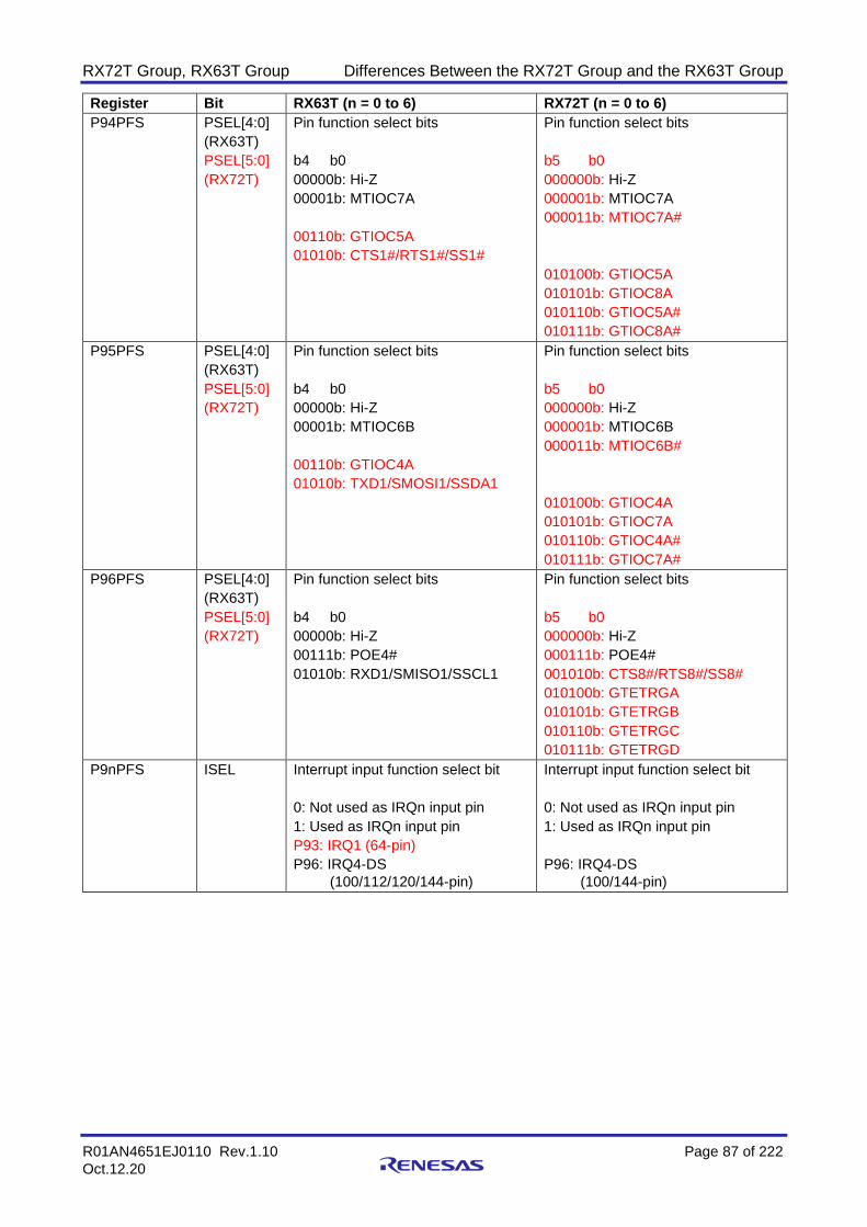
RX72T Group, RX63T Group Differences Between the RX72T Group and the RX63T Group
R01AN4651EJ0110 Rev.1.10 Page 87 of 222
Oct.12.20
Register Bit RX63T (n = 0 to 6) RX72T (n = 0 to 6)
P94PFS PSEL[4:0]
(RX63T)
PSEL[5:0]
(RX72T)
Pin function select bits
b4 b0
00000b: Hi-Z
00001b: MTIOC7A
00110b: GTIOC5A
01010b: CTS1#/RTS1#/SS1#
Pin function select bits
b5 b0
000000b: Hi-Z
000001b: MTIOC7A
000011b: MTIOC7A#
010100b: GTIOC5A
010101b: GTIOC8A
010110b: GTIOC5A#
010111b: GTIOC8A#
P95PFS PSEL[4:0]
(RX63T)
PSEL[5:0]
(RX72T)
Pin function select bits
b4 b0
00000b: Hi-Z
00001b: MTIOC6B
00110b: GTIOC4A
01010b: TXD1/SMOSI1/SSDA1
Pin function select bits
b5 b0
000000b: Hi-Z
000001b: MTIOC6B
000011b: MTIOC6B#
010100b: GTIOC4A
010101b: GTIOC7A
010110b: GTIOC4A#
010111b: GTIOC7A#
P96PFS PSEL[4:0]
(RX63T)
PSEL[5:0]
(RX72T)
Pin function select bits
b4 b0
00000b: Hi-Z
00111b: POE4#
01010b: RXD1/SMISO1/SSCL1
Pin function select bits
b5 b0
000000b: Hi-Z
000111b: POE4#
001010b: CTS8#/RTS8#/SS8#
010100b: GTETRGA
010101b: GTETRGB
010110b: GTETRGC
010111b: GTETRGD
P9nPFS ISEL Interrupt input function select bit
0: Not used as IRQn input pin
1: Used as IRQn input pin
P93: IRQ1 (64-pin)
P96: IRQ4-DS
(100/112/120/144-pin)
Interrupt input function select bit
0: Not used as IRQn input pin
1: Used as IRQn input pin
P96: IRQ4-DS
(100/144-pin)

RX72T Group, RX63T Group Differences Between the RX72T Group and the RX63T Group
R01AN4651EJ0110 Rev.1.10 Page 88 of 222
Oct.12.20
Table 2.47 Comparison of PAn Pin Function Control Register (PAnPFS)
Register Bit RX63T (n = 0 to 6) RX72T (n = 0 to 7)
PA0PFS PSEL[4:0]
(RX63T)
PSEL[5:0]
(RX72T)
Pin function select bits
b4 b0
00000b: Hi-Z
00001b: MTIOC6C
01010b: SCK2
01101b: SSLA3
01110b: SSLB3
Pin function select bits
b5 b0
000000b: Hi-Z
000001b: MTIOC6C
000011b: MTIOC6C#
000101b: TMO2
001010b: SCK9
001011b: TXD11/SMOSI11/
SSDA11
001101b: SSLA3
010000b: CTX0
010001b: USB0_EXICEN
010010b: USB0_VBUSEN
PA1PFS PSEL[4:0]
(RX63T)
PSEL[5:0]
(RX72T)
Pin function select bits
b4 b0
00000b: Hi-Z
00001b: MTIOC6A
01010b: TXD2/SMOSI2/SSDA2
01101b: SSLA2
01110b: SSLB2
Pin function select bits
b5 b0
000000b: Hi-Z
000001b: MTIOC6A
000011b: MTIOC6A#
000101b: TMO4
001001b: ADTRG0#
001010b: TXD9/SMOSI9/SSDA9
001011b: RXD11/SMISO11/
SSCL11
001101b: SSLA2
010000b: CRX0
010001b: USB0_ID
010010b: USB0_OVRCURA
PA2PFS PSEL[4:0]
(RX63T)
PSEL[5:0]
(RX72T)
Pin function select bits
b4 b0
00000b: Hi-Z
00001b: MTIOC2B
01010b: RXD2/MISO2/SSCL2
01101b: SSLA1
01110b: SSLB1
Pin function select bits
b5 b0
000000b: Hi-Z
000001b: MTIOC2B
000011b: MTIOC2B#
000101b: TMO7
001010b: CTS6#/RTS6#/SS6#
001011b: RXD9/SMISO9/SSCL9
001100b: SCK11
001101b: SSLA1
010100b: GTADSM1

RX72T Group, RX63T Group Differences Between the RX72T Group and the RX63T Group
R01AN4651EJ0110 Rev.1.10 Page 89 of 222
Oct.12.20
Register Bit RX63T (n = 0 to 6) RX72T (n = 0 to 7)
PA3PFS PSEL[4:0]
(RX63T)
PSEL[5:0]
(RX72T)
Pin function select bits
b4 b0
00000b: Hi-Z
00001b: MTIOC2A
01010b: SCK0
01101b: SSLA0
01110b: SSLB0
Pin function select bits
b5 b0
000000b: Hi-Z
000001b: MTIOC2A
000011b: MTIOC2A#
000101b: TMRI7
001010b: TXD9/SMOSI9/SSDA9
001011b: SCK8
001101b: SSLA0
010100b: GTADSM0
PA4PFS PSEL[4:0]
(RX63T)
PSEL[5:0]
(RX72T)
Pin function select bits
b4 b0
00000b: Hi-Z
00001b: MTIOC1B
01001b: ADTRG0#
01010b: TXD0/SMOSI0/SSDA0
01101b: RSPCKA
01110b: RSPCKB
Pin function select bits
b5 b0
000000b: Hi-Z
000001b: MTIOC1B
000011b: MTIOC1B#
000101b: TMCI7
001001b: ADTRG0#
001010b: SCK6
001011b: TXD8/SMOSI8/SSDA8
001101b: RSPCKA
PA5PFS PSEL[4:0]
(RX63T)
PSEL[5:0]
(RX72T)
Pin function select bits
b4 b0
00000b: Hi-Z
00001b: MTIOC1A
01001b: ADTRG1#
01010b: RXD0/SMISO0/SSCL0
01101b: MISOA
01110b: MISOB
Pin function select bits
b5 b0
000000b: Hi-Z
000001b: MTIOC1A
000011b: MTIOC1A#
000101b: TMCI3
001001b: ADTRG1#
001010b: RXD6/SMISO6/SSCL6
001011b: RXD8/SMISO8/SSCL8
001101b: MISOA

RX72T Group, RX63T Group Differences Between the RX72T Group and the RX63T Group
R01AN4651EJ0110 Rev.1.10 Page 90 of 222
Oct.12.20
Register Bit RX63T (n = 0 to 6) RX72T (n = 0 to 7)
PA6PFS PSEL[4:0]
(RX63T)
PSEL[5:0]
(RX72T)
Pin function select bits
b4 b0
00000b: Hi-Z
01010b: CTS3#/RTS3#/SS3#
Pin function select bits
b5 b0
000000b: Hi-Z
000001b: MTCLKB
000010b: MTCLKD
000011b: MTCLKB#
000100b: MTCLKD#
000101b: TMO6
001001b: ADSM1
001011b: TXD11/SMOSI11/
SSDA11
001100b: TXD12/SMOSI12/
SSDA12/TXDX12/
SIOX12
010000b: CTX0
010100b: GTADSM1
PA7PFS ⎯ ⎯ PA7 pin function control register
PAnPFS ISEL ⎯ Interrupt input function select bit
Table 2.48 Comparison of PBn Pin Function Control Register (PBnPFS)
Register Bit RX63T (n = 0 to 7) RX72T (n = 0 to 7)
PB0PFS PSEL[4:0]
(RX63T)
PSEL[5:0]
(RX72T)
Pin function select bits
b4 b0
00000b: Hi-Z
00001b: MTIOC0D
01101b: MOSIA
01110b: MOSIB
Pin function select bits
b5 b0
000000b: Hi-Z
000001b: MTIOC0D
000011b: MTIOC0D#
000101b: TMO0
001001b: ADTRG2#
001010b: TXD6/SMOSI6/SSDA6
001011b: CTS11#/RTS11#/SS11#
001101b: MOSIA
PB1PFS PSEL[4:0]
(RX63T)
PSEL[5:0]
(RX72T)
Pin function select bits
b4 b0
00000b: Hi-Z
00001b: MTIOC0C
01010b: RXD0/SMISO0/SSCL0
01111b: SCL0
Pin function select bits
b5 b0
000000b: Hi-Z
000001b: MTIOC0C
000011b: MTIOC0C#
000101b: TMCI0
001001b: ADSM1
001010b: RXD6/SMISO6/SSCL6
001111b: SCL
010100b: GTADSM1

RX72T Group, RX63T Group Differences Between the RX72T Group and the RX63T Group
R01AN4651EJ0110 Rev.1.10 Page 91 of 222
Oct.12.20
Register Bit RX63T (n = 0 to 7) RX72T (n = 0 to 7)
PB2PFS PSEL[4:0]
(RX63T)
PSEL[5:0]
(RX72T)
Pin function select bits
b4 b0
00000b: Hi-Z
00001b: MTIOC0B
01010b: TXD0/SMOSI0/SSDA0
01111b: SDA0
Pin function select bits
b5 b0
000000b: Hi-Z
000001b: MTIOC0B
000011b: MTIOC0B#
000101b: TMRI0
001001b: ADSM0
001010b: TXD6/SMOSI6/SSDA6
001111b: SDA
010100b: GTADSM0
PB3PFS PSEL[4:0]
(RX63T)
PSEL[5:0]
(RX72T)
Pin function select bits
b4 b0
00000b: Hi-Z
00001b: MTIOC0A
00101b: CACREF
01010b: SCK0
Pin function select bits
b5 b0
000000b: Hi-Z
000001b: MTIOC0A
000011b: MTIOC0A#
000111b: CACREF
001010b: SCK6
001101b: RSPCKA
PB4PFS PSEL[4:0]
(RX63T)
PSEL[5:0]
(RX72T)
Pin function select bits
b4 b0
00000b: Hi-Z
00110b: GTETRG0
00111b: POE8#
Pin function select bits
b5 b0
000000b: Hi-Z
000111b: POE8#
001010b: CTS5#/RTS5#/SS5#
001011b: SCK11
001100b: CTS11#/RTS11#/SS11#
010001b: USB0_OVRCURB
010100b: GTETRGA
010101b: GTETRGB
010110b: GTETRGC
010111b: GTETRGD
PB5PFS PSEL[4:0]
(RX63T)
PSEL[5:0]
(RX72T)
Pin function select bits
b4 b0
00000b: Hi-Z
01100b: TXD12/SMOSI12/
SSDA12/TXDX12/SIOX12
10000b: CTX1
Pin function select bits
b5 b0
000000b: Hi-Z
001010b: TXD5/SMOSI5/SSDA5
001011b: TXD11/SMOSI11/
SSDA11
001100b: TXD12/SMOSI12/
SSDA12/TXDX12/
SIOX12
010000b: CTX0
010001b: USB0_VBUSEN
010100b: GTIOC2B
010110b: GTIOC2B#

RX72T Group, RX63T Group Differences Between the RX72T Group and the RX63T Group
R01AN4651EJ0110 Rev.1.10 Page 92 of 222
Oct.12.20
Register Bit RX63T (n = 0 to 7) RX72T (n = 0 to 7)
PB6PFS PSEL[4:0]
(RX63T)
PSEL[5:0]
(RX72T)
Pin function select bits
b4 b0
00000b: Hi-Z
01100b: RXD12/SMISO12/
SSCL12/RXDX12
10000b: CRX1
Pin function select bits
b5 b0
000000b: Hi-Z
001010b: RXD5/SMISO5/SSCL5
001011b: RXD11/SMISO11/
SSCL11
001100b: RXD12/SMISO12/
SSCL12/RXDX12
010000b: CRX0
010001b: USB0_OVRCURA
010100b: GTIOC2A
010110b: GTIOC2A#
PB7PFS PSEL[4:0]
(RX63T)
PSEL[5:0]
(RX72T)
Pin function select bits
b4 b0
00000b: Hi-Z
01100b: SCK12
Pin function select bits
b5 b0
000000b: Hi-Z
001010b: SCK5
001011b: SCK11
001100b: SCK12
010001b: USB0_OVRCURB
010100b: GTIOC1B
010110b: GTIOC1B#
PBnPFS ISEL Interrupt input function select bit
0: Not used as IRQn input pin
1: Used as IRQn input pin
PB1: IRQ4 (100/112/120/144-pin)
PB4: IRQ3-DS
(64/80/100/112/120/144-pin)
PB5: IRQ0 (64/80-pin)
PB6: IRQ2 (100/112/120/144-pin)
Interrupt input function select bit
0: Not used as IRQn input pin
1: Used as IRQn input pin
PB0: IRQ8 (100/144-pin)
PB1: IRQ4 (100/144-pin)
PB3: IRQ9 (100/144-pin)
PB4: IRQ3-DS
(100/144-pin)
PB6: IRQ2 (100/144-pin)
Table 2.49 Comparison of PCn Pin Function Control Register (PCnPFS)
Register Bit RX63T (n = 0 to 5) RX72T (n = 0 to 6)
PCnPFS PSEL[5:0] ⎯ Pin function select bits
ISEL ⎯ Interrupt input function select bit
ASEL Analog input function select bit ⎯

RX72T Group, RX63T Group Differences Between the RX72T Group and the RX63T Group
R01AN4651EJ0110 Rev.1.10 Page 93 of 222
Oct.12.20
Table 2.50 Comparison of PDn Pin Function Control Register (PDnPFS)
Register Bit RX63T (n = 0 to 7) RX72T (n = 0 to 7)
PD0PFS PSEL[4:0]
(RX63T)
PSEL[5:0]
(RX72T)
Pin function select bits
b4 b0
00000b: Hi-Z
00110b: GTIOC3B
01101b: RSPCKA
01110b: RSPCKB
Pin function select bits
b5 b0
000000b: Hi-Z
000001b: MTIOC9C
000011b: MTIOC9C#
000101b: TMO1
001001b: ADST0
001010b: CTS1#/RTS1#/SS1#
001011b: CTS11#/RTS11#/SS11#
001101b: SSLA0
010100b: GTIOC0B
010101b: GTIOC3B
010110b: GTIOC0B#
010111b: GTIOC3B#
PD1PFS PSEL[4:0]
(RX63T)
PSEL[5:0]
(RX72T)
Pin function select bits
b4 b0
00000b: Hi-Z
00110b: GTIOC3A
01101b: MISOA
01110b: MISOB
10001b: USB0_EXICEN
Pin function select bits
b5 b0
000000b: Hi-Z
000001b: MTIOC9A
000011b: MTIOC9A#
000101b: TMRI1
000110b: TMRI5
001010b: TXD5/SMOSI5/SSDA5
001101b: SSLA1
010000b: CTX0
010100b: GTIOC0A
010101b: GTIOC3A
010110b: GTIOC0A#
010111b: GTIOC3A#
PD2PFS PSEL[4:0]
(RX63T)
PSEL[5:0]
(RX72T)
Pin function select bits
b4 b0
00000b: Hi-Z
00110b: GTIOC2B
01101b: MOSIA
01110b: MOSIB
10001b: USB0_ID
Pin function select bits
b5 b0
000000b: Hi-Z
000101b: TMO6
001011b: TXD8/SMOSI8/SSDA8
001101b: RSPCKA
010100b: GTIOC3B
010101b: GTIOC1A
010110b: GTIOC3B#
010111b: GTIOC1A#

RX72T Group, RX63T Group Differences Between the RX72T Group and the RX63T Group
R01AN4651EJ0110 Rev.1.10 Page 94 of 222
Oct.12.20
Register Bit RX63T (n = 0 to 7) RX72T (n = 0 to 7)
PD3PFS PSEL[4:0]
(RX63T)
PSEL[5:0]
(RX72T)
Pin function select bits
b4 b0
00000b: Hi-Z
00110b: GTIOC2A
01010b: TXD1/SMOSI1/SSDA1
Pin function select bits
b5 b0
000000b: Hi-Z
000101b: TMO2
001011b: RXD8/SMISO8/SSCL8
001101b: MISOA
010100b: GTIOC3A
010101b: GTIOC0B
010110b: GTIOC3A#
010111b: GTIOC0B#
PD4PFS PSEL[4:0]
(RX63T)
PSEL[5:0]
(RX72T)
Pin function select bits
b4 b0
00000b: Hi-Z
00110b: GTIOC1B
01010b: SCK1
Pin function select bits
b5 b0
000000b: Hi-Z
000101b: TMCI1
000110b: TMO4
001010b: SCK5
001011b: SCK8
001101b: MOSIA
010001b: USB0_VBUS
010100b: GTIOC2B
010101b: GTIOC0A
010110b: GTIOC2B#
010111b: GTIOC0A#
PD5PFS PSEL[4:0]
(RX63T)
PSEL[5:0]
(RX72T)
Pin function select bits
b4 b0
00000b: Hi-Z
00110b: GTIOC1A
01010b: RXD1/SMISO1/SSCL1
Pin function select bits
b5 b0
000000b: Hi-Z
000101b: TMO0
001010b: TXD1/SMOSI1/SSDA1
001011b: TXD11/SMOSI11/
SSDA11
010100b: GTIOC2A
010101b: GTETRGC
010110b: GTIOC2A#
PD6PFS PSEL[4:0]
(RX63T)
PSEL[5:0]
(RX72T)
Pin function select bits
b4 b0
00000b: Hi-Z
00110b: GTIOC0B
01101b: SSLA0
01110b: SSLB0
Pin function select bits
b5 b0
000000b: Hi-Z
000101b: TMCI0
000110b: TMCI6
001010b: SCK1
001011b: SCK11
010100b: GTIOC1B
010101b: GTETRGB
010110b: GTIOC1B#

RX72T Group, RX63T Group Differences Between the RX72T Group and the RX63T Group
R01AN4651EJ0110 Rev.1.10 Page 95 of 222
Oct.12.20
Register Bit RX63T (n = 0 to 7) RX72T (n = 0 to 7)
PD7PFS PSEL[4:0]
(RX63T)
PSEL[5:0]
(RX72T)
Pin function select bits
b4 b0
00000b: Hi-Z
00110b: GTIOC0A
01010b: CTS0#/RTS0#/SS0#
01101b: SSLA1
01110b: SSLB1
10000b: CTX1
Pin function select bits
b5 b0
000000b: Hi-Z
000101b: TMRI0
000110b: TMRI6
001010b: RXD1/SMISO1/SSCL1
001011b: RXD11/SMISO11/
SSCL11
010100b: GTIOC1A
010101b: GTETRGA
010110b: GTIOC1A#
PDnPFS ISEL Interrupt input function select bit
0: Not used as IRQn input pin
1: Used as IRQn input pin
PD5: IRQ6 (100/112/120/144-pin)
Interrupt input function select bit
0: Not used as IRQn input pin
1: Used as IRQn input pin
PD4: IRQ2 (100/144-pin)
PD5: IRQ6 (100/144-pin)
PD6: IRQ5 (100/144-pin)
PD7: IRQ8 (100/144-pin)
Table 2.51 Comparison of PEn Pin Function Control Register (PEnPFS)
Register Bit RX63T (n = 0 to 5) RX72T (n = 0 to 6)
PE0PFS PSEL[4:0]
(RX63T)
PSEL[5:0]
(RX72T)
Pin function select bits
b4 b0
00000b: Hi-Z
01101b: SSLA2
01110b: SSLB2
10000b: CRX1
10001b: USB0_OVRCURB
Pin function select bits
b5 b0
000000b: Hi-Z
000001b: MTIOC9B
000011b: MTIOC9B#
000101b: TMCI1
000110b: TMCI5
001010b: RXD5/SMISO5/SSCL5
001101b: SSLA2
010000b: CRX0
010001b: USB0_OVRCURB
PE1PFS PSEL[4:0]
(RX63T)
PSEL[5:0]
(RX72T)
Pin function select bits
b4 b0
00000b: Hi-Z
01100b: CTS12#/RTS12#/SS12#
01101b: SSLA3
01110b: SSLB3
10001b: USB0_OVRCURA
Pin function select bits
b5 b0
000000b: Hi-Z
000001b: MTIOC9D
000011b: MTIOC9D#
000101b: TMO5
001010b: CTS5#/RTS5#/SS5#
001100b: CTS12#/RTS12#/SS12#
001101b: SSLA3

RX72T Group, RX63T Group Differences Between the RX72T Group and the RX63T Group
R01AN4651EJ0110 Rev.1.10 Page 96 of 222
Oct.12.20
Register Bit RX63T (n = 0 to 5) RX72T (n = 0 to 6)
PE2PFS PSEL[4:0]
(RX63T)
PSEL[5:0]
(RX72T)
Pin function select bits
b4 b0
00000b: Hi-Z
00111b: POE10#
Pin function select bits
b5 b0
000000b: Hi-Z
000111b: POE10#
PE3PFS PSEL[4:0]
(RX63T)
PSEL[5:0]
(RX72T)
Pin function select bits
b4 b0
00000b: Hi-Z
00010b: MTICLKD
00111b: POE11#
Pin function select bits
b5 b0
000000b: Hi-Z
000010b: MTCLKD
000100b: MTCLKD#
000111b: POE11#
001010b: CTS9#/RTS9#/SS9#
010100b: GTETRGA
010101b: GTETRGB
010110b: GTETRGC
010111b: GTETRGD
PE4PFS PSEL[4:0]
(RX63T)
PSEL[5:0]
(RX72T)
Pin function select bits
b4 b0
00000b: Hi-Z
00010b: MTICLKC
00111b: POE10#
Pin function select bits
b5 b0
000000b: Hi-Z
000010b: MTCLKC
000100b: MTCLKC#
000111b: POE10#
001010b: SCK9
010100b: GTETRGA
010101b: GTETRGB
010110b: GTETRGC
010111b: GTETRGD
PE5PFS PSEL[4:0]
(RX63T)
PSEL[5:0]
(RX72T)
Pin function select bits
b4 b0
00000b: Hi-Z
10001b: USB0_VBUS
Pin function select bits
b5 b0
000000b: Hi-Z
000001b: MTIOC9D
000011b: MTIOC9D#
001001b: ADST0
001010b: SCK9
001011b: CTS9#/RTS9#/SS9#
010100b: GTIOC3A
010101b: GTETRGB
010110b: GTIOC3A#
010111b: GTETRGD
PE6PFS ⎯ ⎯ PE6 pin function control register

RX72T Group, RX63T Group Differences Between the RX72T Group and the RX63T Group
R01AN4651EJ0110 Rev.1.10 Page 97 of 222
Oct.12.20
Register Bit RX63T (n = 0 to 5) RX72T (n = 0 to 6)
PEnPFS ISEL Interrupt input function select bit
0: Not used as IRQn input pin
1: Used as IRQn input pin
PE0: IRQ7 (100/112/120/144-pin)
PE3: IRQ2-DS (100/112/120/
144-pin)
PE4: IRQ1 (100/112/120/144-pin)
PE5: IRQ0 (100/112/120/144-pin)
Interrupt input function select bit
0: Not used as IRQn input pin
1: Used as IRQn input pin
PE0: IRQ7 (100/144-pin)
PE1: IRQ15 (100/144-pin)
PE3: IRQ2-DS (100/144-pin)
PE4: IRQ1 (100/144-pin)
PE5: IRQ0 (100/144-pin)
PE6: IRQ3 (144-pin)
Table 2.52 Comparison of PFn Pin Function Control Register (PFnPFS)
Register Bit RX63T (n = 2, 3) RX72T (n = 0 to 3)
PF0PFS ⎯ ⎯ PF0 pin function control register
PF1PFS ⎯ ⎯ PF1 pin function control register
PF2PFS PSEL[4:0]
(RX63T)
PSEL[5:0]
(RX72T)
Pin function select bits
b4 b0
00000b: Hi-Z
01010b: RXD1/SMISO1/SSCL1
Pin function select bits
b5 b0
000000b: Hi-Z
000101b: TMO3
001011b: SCK11
010000b: CTX0
010100b: GTETRGB
011110b: COMP1
PF3PFS PSEL[4:0]
(RX63T)
PSEL[5:0]
(RX72T)
Pin function select bits
b4 b0
00000b: Hi-Z
01010b: TXD1/SMOSI1/SSDA1
Pin function select bits
b5 b0
000000b: Hi-Z
000101b: TMO7
001011b: CTS11#/RTS11#/SS11#
010000b: CRX0
010100b: GTETRGA
011110b: COMP0
PFnPFS ISEL Interrupt input function select bit
0: Not used as IRQn input pin
1: Used as IRQn input pin
PF2: IRQ5 (112/120/144-pin)
Interrupt input function select bit
0: Not used as IRQn input pin
1: Used as IRQn input pin
PF0: IRQ12 (144-pin)
PF1: IRQ13 (144-pin)
PF2: IRQ5 (144-pin)
PF3: IRQ14 (144-pin)

RX72T Group, RX63T Group Differences Between the RX72T Group and the RX63T Group
R01AN4651EJ0110 Rev.1.10 Page 98 of 222
Oct.12.20
Table 2.53 Comparison of PGn Pin Function Control Register (PGnPFS)
Register Bit RX63T (n = 0 to 6) RX72T (n = 0 to 2)
PG0PFS PSEL[4:0]
(RX63T)
PSEL[5:0]
(RX72T)
Pin function select bits
b4 b0
00000b: Hi-Z
00110b: GTIOC7A
01010b: TXD2/SMOSI2/SSDA2
Pin function select bits
b5 b0
000000b: Hi-Z
001010b: RXD9/SMISO9/SSCL9
010101b: GTIOC1B
010111b: GTIOC1B#
011110b: COMP2
PG1PFS PSEL[4:0]
(RX63T)
PSEL[5:0]
(RX72T)
Pin function select bits
b4 b0
00000b: Hi-Z
00110b: GTIOC7B
01010b: RXD2/SMISO2/SSCL2
Pin function select bits
b5 b0
000000b: Hi-Z
001010b: TXD9/SMOSI9/SSDA9
010101b: GTIOC0A
010111b: GTIOC0A#
011110b: COMP1
PG2PFS PSEL[4:0]
(RX63T)
PSEL[5:0]
(RX72T)
Pin function select bits
b4 b0
00000b: Hi-Z
01010b: SCK2
Pin function select bits
b5 b0
000000b: Hi-Z
001010b: SCK9
010100b: GTETRGA
010101b: GTIOC0B
010111b: GTIOC0B#
011110b: COMP0
PG3PFS ⎯ PG3 pin function control register ⎯
PG4PFS ⎯ PG4 pin function control register ⎯
PG5PFS ⎯ PG5 pin function control register ⎯
PG6PFS ⎯ PG6 pin function control register ⎯
PGnPFS ISEL Interrupt input function select bit
0: Not used as IRQn input pin
1: Used as IRQn input pin
PG0: IRQ0 (112/120/144-pin)
PG1: IRQ1 (112/120/144-pin)
PG2: IRQ2 (112/120/144-pin)
PG4: IRQ6 (112/120/144-pin)
Interrupt input function select bit
0: Not used as IRQn input pin
1: Used as IRQn input pin
PG0: IRQ0 (144-pin)
PG1: IRQ1 (144-pin)
PG2: IRQ2 (144-pin)
Table 2.54 Comparison of PHn Pin Function Control Register (PHnPFS)
Register Bit RX63T RX72T
PHnPFS ⎯ ⎯ PHn pin function control register
(n = 0 to 7)
Table 2.55 Comparison of PKn Pin Function Control Register (PKnPFS)
Register Bit RX63T RX72T
PKnPFS ⎯ ⎯ PKn pin function control register
(n = 0 to 2)

RX72T Group, RX63T Group Differences Between the RX72T Group and the RX63T Group
R01AN4651EJ0110 Rev.1.10 Page 99 of 222
Oct.12.20
Table 2.56 Comparison of Multi-Function Pin Controller Registers
Register Bit RX63T (MPC) RX72T (MPC)
UDPUPEPFS ⎯ USB0_DPUPE pin function control
register
—
PFCSS0 CS0S CS0# output pin select bit
0: Set P26 as CS0# output pin.
1: Set PD1 as CS0# output pin.
CS0# output pin select bit
0: Set P96 as CS0# output pin.
1: Set PC0 as CS0# output pin.
CS1S[1:0] CS1# output pin select bits
b3 b2
0 0: Set P00 as CS1# output pin.
0 1: Set P25 as CS1# output pin.
1 x: Set PF2 as CS1# output pin.
CS1# output pin select bits
b3 b2
0 0: Set P80 as CS1# output pin.
0 1: Set PK0 as CS1# output pin.
1 0: Set PF1 as CS1# output pin.
1 1: Set PC2 as CS1# output pin.
CS2S[1:0] CS2# output pin select bits
b5 b4
0 0: Set PD2 as CS2# output pin.
0 1: Set PG6 as CS2# output pin.
1 x: Set P05 as CS2# output pin.
CS2# output pin select bits
b5 b4
0 0: Set P81 as CS2# output pin.
0 1: Set P26 as CS2# output pin.
1 x: Set PF2 as CS2# output pin.
CS3S[1:0]
(RX63T)
CS3S
(RX72T)
CS3# output pin select bits
(b7 to b6)
b7 b6
0 0: Set P12 as CS3# output pin.
0 1: Set PF4 as CS3# output pin.
1 x: Set PA6 as CS3# output pin.
CS3# output pin select bits
(b6)
0: Set PF3 as CS3# output pin.
1: Set P25 as CS3# output pin.
PFAOE1 A20E ⎯ Address A20 output enable
PFBCR0 ADRLE A0 to A7 output enable bit
0: P65 to P60, P53, and P52 are
set as I/O port pins.
1: P65 to P60, P53, and P52 are
set as external address bus A0
to A7.
A0 to A7 output enable bit
0: PB0, PA2, PF0, PA3 to PA5,
PB0 to PB3, PB4 to PB7, and
PD0 to PD2 are set as I/O port
pins.
1: PB0, PA2, PF0, PA3 to PA5,
PB0 to PB3, PB4 to PB7, and
PD0 to PD2 are set as external
address bus A0 to A7.
ADRHMS ⎯ A12 to A20 output selection bit
BCLKO ⎯ BCLK forced output bit
DHE D8 to D15 output enable bit
0: P32 to P30 and P24 to P20 are
set as I/O port pins.
1: P32 to P30 and P24 to P20 are
set as external data bus D8 to
D15.
D8 to D15 output enable bit
0: Disables output of external data
bus D8 to D15 (set as I/O port).
1: Enables output of external data
bus D8 to D15.
D8 to D10: P32 to P30
D11 to D15: Selected by
PFBCR2 register.

RX72T Group, RX63T Group Differences Between the RX72T Group and the RX63T Group
R01AN4651EJ0110 Rev.1.10 Page 100 of 222
Oct.12.20
Register Bit RX63T (MPC) RX72T (MPC)
PFBCR1 WAITS[1:0] WAIT select bits
b1 b0
0 0: PE0 is set as WAIT# input pin.
0 1: P82 is set as WAIT# input pin.
1 x: P05 is set as WAIT# input pin.
WAIT select bits
b1 b0
0 0: P82, PE0, and P96 are not set
as WAIT# input pin.
0 1: P82 is set as WAIT# input pin.
1 0: PE0 is set as WAIT# input pin.
1 1: P96 is set as WAIT# input pin.
PFBCR2 ⎯ ⎯ External bus control register 2
PFBCR3 ⎯ ⎯ External bus control register 3
PFBCR4 ⎯ ⎯ External bus control register 4
PFUSB0 ⎯ USB0 control register ⎯

RX72T Group, RX63T Group Differences Between the RX72T Group and the RX63T Group
R01AN4651EJ0110 Rev.1.10 Page 101 of 222
Oct.12.20
2.18 Multi-Function Timer Pulse Unit 3
Table 2.57 is a comparative overview of multi-function timer pulse unit 3, Table 2.58 is a comparison of multi-function timer pulse unit 3 registers, and Table 2.59 and Table 2.60 are comparative listings of TPSC bit settings.
Table 2.57 Comparative Overview of Multi-Function Timer Pulse Unit 3
Item RX63T (MTU3) RX72T (MTU3d)
Pulse input/output [144-, 120-, 112-, and 100-pin versions]
Max. 24 lines
[64- and 48-pin versions]
Max. 24 lines (Up to 16 lines can be
used simultaneously.)
Max. 28 lines
Pulse input 3 lines 3 lines
Count clock Six to eight clocks for each channel (four
clocks for channel 5)
11 clocks for each channel (14 clocks for
MTU0 and MTU9, 12 clocks for MTU2,
10 clocks for MTU5, and four clocks for
MTU1 and MTU2 (when LWA = 1))
Operating
frequency
8 to 100 MHz Up to 200 MHz
Available
operations
[MTU0 to MTU4, MTU6, and MTU7]
• Waveform output at compare match
• Input capture function
• Counter-clearing operation
• Simultaneous writing to multiple timer
counters (TCNT)
• Simultaneous clearing at compare
match or input capture
• Simultaneous input and output to
registers in synchronization with
counter operations
[144-, 120-, 112-, and 100-pin versions]
• Up to 12-phase PWM output in
combination with synchronous
operation
[64- and 48-pin versions]
• Up to 8-phase PWM output in
combination with synchronous
operation
[MTU0 to MTU4, MTU6, MTU7, and
MTU9]
• Waveform output at compare match
• Input capture function (noise filter
setting available)
• Counter-clearing operation
• Simultaneous writing to multiple timer
counters (TCNT)
• Simultaneous clearing at compare
match or input capture
• Simultaneous input and output to
registers in synchronization with
counter operations
• Up to 14-phase PWM output in
combination with synchronous
operation
[MTU0, MTU3, MTU4, MTU6, and
MTU7]
Buffer operation available
[MTU0, MTU3, MTU4, MTU6, MTU7,
and MTU9]
Buffer operation available

RX72T Group, RX63T Group Differences Between the RX72T Group and the RX63T Group
R01AN4651EJ0110 Rev.1.10 Page 102 of 222
Oct.12.20
Item RX63T (MTU3) RX72T (MTU3d)
Available
operations
[MTU3, MTU4, MTU6, and MTU7]
• Through interlocked operation of
MTU3/MTU 4 and MTU6/MTU7,
positive and negative signals in three
phases (6 phases in total) can be
output in complementary PWM and
reset PWM operation.
• In complementary PWM mode,
values can be transferred from buffer
registers to temporary registers at
timer-counter peaks or troughs or
when the buffer registers
(MTU4.TGRD and MTU7.TGRD) are
written to.
• Double-buffering is selectable in
complementary PWM mode.
[MTU3, MTU4, MTU6, and MTU7]
• Through interlocked operation of
MTU3/MTU 4 and MTU6/MTU7,
positive and negative signals in six
phases (12 phases in total) can be
output in complementary PWM and
reset-synchronized PWM operation.
• In complementary PWM mode,
values can be transferred from buffer
registers to temporary registers at
timer-counter peaks or troughs or
when the buffer registers
(MTU4.TGRD and MTU7.TGRD) are
written to.
• Double-buffering is selectable in
complementary PWM mode.
[MTU1, MTU2]
• Phase counting mode can be
specified independently
• Cascade connection operation
available
[MTU1, MTU2]
• Phase counting mode can be
specified independently
• 32-bit phase counting mode can be
specified for interlocked operation of
MTU1 and MTU2 (when
TMDR3.LWA = 1)
• Cascade connection operation
available
[MTU3, MTU4]
A mode for driving AC synchronous
motors (brushless DC motors) through
interlocking with MTU0 and using
complementary PWM output and reset
PWM output is available, allowing
selection between two types of
waveform output (chopping or level).
[MTU3, MTU4]
A mode for driving AC synchronous
motors (brushless DC motors) through
interlocking with MTU0 and using
complementary PWM output and reset-
synchronized PWM output is available,
allowing selection between two types of
waveform output (chopping or level).
[MTU5]
Ability to operate as a dead-time
compensation counter
[MTU5]
Ability to operate as a dead-time
compensation counter
⎯ [MTU6, MTU7]
A mode for driving AC synchronous
motors (brushless DC motors) through
interlocking with MTU9 and using
complementary PWM output and reset-
synchronized PWM output is available,
allowing selection between two types of
waveform output (chopping or level).
Interrupt skipping
function
In complementary PWM mode, interrupts
on crests and troughs of counter values
and triggers to start conversion by the
A/D converter can be skipped.
In complementary PWM mode, interrupts
on crests and troughs of counter values
and triggers to start conversion by the
A/D converter can be skipped.
Interrupt sources 38 sources 45 sources
Buffer operation Automatic transfer of register data
(transfer from buffer register to timer
register)
Automatic transfer of register data
(transfer from buffer register to timer
register)

RX72T Group, RX63T Group Differences Between the RX72T Group and the RX63T Group
R01AN4651EJ0110 Rev.1.10 Page 103 of 222
Oct.12.20
Item RX63T (MTU3) RX72T (MTU3d)
Trigger generation A/D converter start triggers can be
generated.
A/D converter start triggers can be
generated.
A/D converter start request delaying
function enables A/D converter to be
started with any desired timing and to be
synchronized with PWM output.
A/D converter start request delaying
function enables A/D converter to be
started with any desired timing and to be
synchronized with PWM output.
Low power
consumption
function
Ability to specify transition to module
stop state
Ability to specify transition to module
stop state
Complementary
PWM mode
Only when using the double buffer
function, a value of (output PWM duty
value − 1) is set in the buffer registers
(MTU3.TGRE, MTU4.TGRE, and
MTU4.TGRF (MTU6.TGRE,
MTU7.TGRE, and MTU7.TGRF)).
Only when using the double buffer
function, a value of (output PWM duty
value) is set in the buffer registers
(MTU3.TGRE, MTU4.TGRE, and
MTU4.TGRF (MTU6.TGRE,
MTU7.TGRE, and MTU7.TGRF)).
A/D conversion
start request frame
synchronization
signal function
None Available
Table 2.58 Comparison of Multi-Function Timer Pulse Unit 3 Registers
Register Bit RX63T (MTU3) RX72T (MTU3d)
TCR TPSC[2:0]
TPSC[1:0]
Time prescaler select bits
Refer to Table 2.59 and Table 2.60
for details.
Time prescaler select bits
Refer to Table 2.59 and Table 2.60
for details.
TCR2 ⎯ ⎯ Timer control register 2
TMDR1 MD[3:0] Mode select bits
b3 b0
0 0 0 0: Normal mode
0 0 0 1: Setting prohibited
0 0 1 0: PWM mode 1
0 0 1 1: PWM mode 2
0 1 0 0: Phase counting mode 1
0 1 0 1: Phase counting mode 2
0 1 1 0: Phase counting mode 3
0 1 1 1: Phase counting mode 4
1 0 0 0: Reset-synchronized PWM
mode
1 0 0 1: Setting prohibited
1 0 1 x: Setting prohibited
1 1 0 0: Setting prohibited
1 1 0 1: Complementary PWM
mode 1
(transfer at crest)
1 1 1 0: Complementary PWM
mode 2
(transfer at trough)
1 1 1 1: Complementary PWM
mode 3
(transfer at crest and
trough)
x: Don’t care
Mode select bits
b3 b0
0 0 0 0: Normal mode
0 0 0 1: Setting prohibited
0 0 1 0: PWM mode 1
0 0 1 1: PWM mode 2
0 1 0 0: Phase counting mode 1
0 1 0 1: Phase counting mode 2
0 1 1 0: Phase counting mode 3
0 1 1 1: Phase counting mode 4
1 0 0 0: Reset-synchronized PWM
mode
1 0 0 1: Phase counting mode 5
1 0 1 x: Setting prohibited
1 1 0 0: Setting prohibited
1 1 0 1: Complementary PWM
mode 1
(transfer at crest)
1 1 1 0: Complementary PWM
mode 2
(transfer at trough)
1 1 1 1: Complementary PWM
mode 3
(transfer at crest and
trough)
x: Don’t care

RX72T Group, RX63T Group Differences Between the RX72T Group and the RX63T Group
R01AN4651EJ0110 Rev.1.10 Page 104 of 222
Oct.12.20
Register Bit RX63T (MTU3) RX72T (MTU3d)
TMDR3 ⎯ ⎯ Timer mode register 3
TSR TSR TGFA Input capture/output compare flag
A
⎯
TGFB Input capture/output compare flag
B
⎯
TGFC Input capture/output compare flag
C
⎯
TGFD Input capture/output compare flag
D
⎯
TCFV Overflow flag ⎯
TCFU Underflow flag ⎯
CMFW5 Compare match/input capture flag
W5
⎯
CMFV5 Compare match/input capture flag
V5
⎯
CMFU5 Compare match/input capture flag
U5
⎯
TSR2 TGFE Compare match flag E ⎯
TGFF Compare match flag F ⎯
TCNTLW ⎯ ⎯ Timer longword counter
TGRALW,
TGRBLW
⎯ ⎯ Timer longword general registers
TSTRA CST9 ⎯ Counter start 9 bit
TSYRA SYNC9 ⎯ Timer synchronous operation 9 bit
TCSYSTR SCH9 ⎯ Synchronous start 9 bit
TGCRB ⎯ ⎯ Timer gate control register
NFCRn ⎯ ⎯ Noise filter control register n
(n = 0 to 4, 6, 7, 9, C)
NFCR5 ⎯ ⎯ Noise filter control register 5
TADSTRGR0 ⎯ ⎯ A/D conversion start request select
register 0
TADSTRGR1 ⎯ ⎯ A/D conversion start request select
register 1

RX72T Group, RX63T Group Differences Between the RX72T Group and the RX63T Group
R01AN4651EJ0110 Rev.1.10 Page 105 of 222
Oct.12.20
Table 2.59 Comparison of TPSC Bit Settings (Other Than MTU5)
Channel
RX63T (MTU3) RX72T (MTU3d)
TCR.
TPSC
[2:0] Description
TCR2.
TPSC2
[2:0]
TCR.
TPSC
[2:0] Description
MTU0
(RX63T)
MTU0,
MTU9
(RX72T)
0 0 0 Internal clock:
counts on PCLKA/1
0 0 0 0 0 0 Internal clock:
counts on PCLKC/1
0 0 1 Internal clock:
counts on PCLKA/4
0 0 0 0 0 1 Internal clock:
counts on PCLKC/4
0 1 0 Internal clock:
counts on PCLKA/16
0 0 0 0 1 0 Internal clock:
counts on PCLKC/16
0 1 1 Internal clock:
counts on PCLKA/64
0 0 0 0 1 1 Internal clock:
counts on PCLKC/64
1 0 0 External clock:
counts on MTCLKA pin input
0 0 0 1 0 0 External clock:
counts on MTCLKA pin input
1 0 1 External clock:
counts on MTCLKB pin input
0 0 0 1 0 1 External clock:
counts on MTCLKB pin input
1 1 0 External clock:
counts on MTCLKC pin input
0 0 0 1 1 0 External clock:
counts on MTCLKC pin input
1 1 1 External clock:
counts on MTCLKD pin input
0 0 0 1 1 1 External clock:
counts on MTCLKD pin input
0 0 1 x x x Internal clock:
counts on PCLKC/2
0 1 0 x x x Internal clock:
counts on PCLKC/8
0 1 1 x x x Internal clock:
counts on PCLKC/32
1 0 0 x x x Internal clock:
counts on PCLKC/256
1 0 1 x x x Internal clock:
counts on PCLKC/1024
1 1 0 x x x Setting prohibited
1 1 1 x x x External clock:
counts on MTIOC1A pin input
MTU1 0 0 0 Internal clock:
counts on PCLKA/1
0 0 0 0 0 0 Internal clock:
counts on PCLKC/1
0 0 1 Internal clock:
counts on PCLKA/4
0 0 0 0 0 1 Internal clock:
counts on PCLKC/4
0 1 0 Internal clock:
counts on PCLKA/16
0 0 0 0 1 0 Internal clock:
counts on PCLKC/16
0 1 1 Internal clock:
counts on PCLKA/64
0 0 0 0 1 1 Internal clock:
counts on PCLKC/64
1 0 0 External clock:
counts on MTCLKA pin input
0 0 0 1 0 0 External clock:
counts on MTCLKA pin input

RX72T Group, RX63T Group Differences Between the RX72T Group and the RX63T Group
R01AN4651EJ0110 Rev.1.10 Page 106 of 222
Oct.12.20
Channel
RX63T (MTU3) RX72T (MTU3d)
TCR.
TPSC
[2:0] Description
TCR2.
TPSC2
[2:0]
TCR.
TPSC
[2:0] Description
MTU1 1 0 1 External clock:
counts on MTCLKB pin input
0 0 0 1 0 1 External clock:
counts on MTCLKB pin input
1 1 0 Internal clock:
counts on PCLKA/256
0 0 0 1 1 0 Internal clock:
counts on PCLKC/256
1 1 1 Counts on MTU2.TCNT
overflow/underflow
0 0 0 1 1 1 Counts on MTU2.TCNT
overflow/underflow
0 0 1 x x x Internal clock:
counts on PCLKC/2
0 1 0 x x x Internal clock:
counts on PCLKC/8
0 1 1 x x x Internal clock:
counts on PCLKC/32
1 0 0 x x x Internal clock:
counts on PCLKC/1024
1 0 1 x x x Setting prohibited
1 1 0 x x x Setting prohibited
1 1 1 x x x Setting prohibited
MTU2 0 0 0 Internal clock:
counts on PCLKA/1
0 0 0 0 0 0 Internal clock:
counts on PCLKC/1
0 0 1 Internal clock:
counts on PCLKA/4
0 0 0 0 0 1 Internal clock:
counts on PCLKC/4
0 1 0 Internal clock:
counts on PCLKA/16
0 0 0 0 1 0 Internal clock:
counts on PCLKC/16
0 1 1 Internal clock:
counts on PCLKA/64
0 0 0 0 1 1 Internal clock:
counts on PCLKC/64
1 0 0 External clock:
counts on MTCLKA pin input
0 0 0 1 0 0 External clock:
counts on MTCLKA pin input
1 0 1 External clock:
counts on MTCLKB pin input
0 0 0 1 0 1 External clock:
counts on MTCLKB pin input
1 1 0 External clock:
counts on MTCLKC pin input
0 0 0 1 1 0 External clock:
counts on MTCLKC pin input
1 1 1 Internal clock:
counts on PCLKA/1024
0 0 0 1 1 1 Internal clock:
counts on PCLKC/1024
0 0 1 x x x Internal clock:
counts on PCLKC/2
0 1 0 x x x Internal clock:
counts on PCLKC/8
0 1 1 x x x Internal clock:
counts on PCLKC/32
1 0 0 x x x Internal clock:
counts on PCLKC/256
1 0 1 x x x Setting prohibited
1 1 0 x x x Setting prohibited
1 1 1 x x x Setting prohibited
MTU3
MTU4
MTU6
MTU7
0 0 0 Internal clock:
counts on PCLKA/1
0 0 0 0 0 0 Internal clock:
counts on PCLKC/1
0 0 1 Internal clock:
counts on PCLKA/4
0 0 0 0 0 1 Internal clock:
counts on PCLKC/4
0 1 0 Internal clock:
counts on PCLKA/16
0 0 0 0 1 0 Internal clock:
counts on PCLKC/16
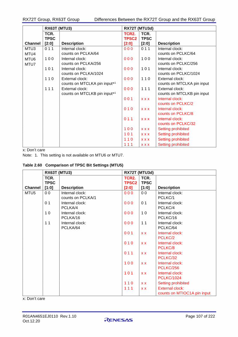
RX72T Group, RX63T Group Differences Between the RX72T Group and the RX63T Group
R01AN4651EJ0110 Rev.1.10 Page 107 of 222
Oct.12.20
Channel
RX63T (MTU3) RX72T (MTU3d)
TCR.
TPSC
[2:0] Description
TCR2.
TPSC2
[2:0]
TCR.
TPSC
[2:0] Description
MTU3
MTU4
MTU6
MTU7
0 1 1 Internal clock:
counts on PCLKA/64
0 0 0 0 1 1 Internal clock:
counts on PCLKC/64
1 0 0 Internal clock:
counts on PCLKA/256
0 0 0 1 0 0 Internal clock:
counts on PCLKC/256
1 0 1 Internal clock:
counts on PCLKA/1024
0 0 0 1 0 1 Internal clock:
counts on PCLKC/1024
1 1 0 External clock:
counts on MTCLKA pin input*1
0 0 0 1 1 0 External clock:
counts on MTCLKA pin input
1 1 1 External clock:
counts on MTCLKB pin input*1
0 0 0 1 1 1 External clock:
counts on MTCLKB pin input
0 0 1 x x x Internal clock:
counts on PCLKC/2
0 1 0 x x x Internal clock:
counts on PCLKC/8
0 1 1 x x x Internal clock:
counts on PCLKC/32
1 0 0 x x x Setting prohibited
1 0 1 x x x Setting prohibited
1 1 0 x x x Setting prohibited
1 1 1 x x x Setting prohibited
x: Don’t care
Note: 1. This setting is not available on MTU6 or MTU7.
Table 2.60 Comparison of TPSC Bit Settings (MTU5)
Channel
RX63T (MTU3) RX72T (MTU3d)
TCR.
TPSC
[1:0] Description
TCR2.
TPSC2
[2:0]
TCR.
TPSC
[1:0] Description
MTU5 0 0 Internal clock:
counts on PCLKA/1
0 0 0 0 0 Internal clock:
PCLKC/1
0 1 Internal clock:
PCLKA/4
0 0 0 0 1 Internal clock:
PCLKC/4
1 0 Internal clock:
PCLKA/16
0 0 0 1 0 Internal clock:
PCLKC/16
1 1 Internal clock:
PCLKA/64
0 0 0 1 1 Internal clock:
PCLKC/64
0 0 1 x x Internal clock:
PCLKC/2
0 1 0 x x Internal clock:
PCLKC/8
0 1 1 x x Internal clock:
PCLKC/32
1 0 0 x x Internal clock:
PCLKC/256
1 0 1 x x Internal clock:
PCLKC/1024
1 1 0 x x Setting prohibited
1 1 1 x x External clock:
counts on MTIOC1A pin input
x: Don’t care

RX72T Group, RX63T Group Differences Between the RX72T Group and the RX63T Group
R01AN4651EJ0110 Rev.1.10 Page 108 of 222
Oct.12.20
2.19 Port Output Enable 3
Table 2.61 is a comparative overview of port output enable 3, and Table 2.62 is a comparison of port output enable 3 registers.
Table 2.61 Comparative Overview of Port Output Enable 3
Item RX63T (POE3) RX72T (POE3B)
Functions • Input pins POE0#, POE4#, POE8#,
POE10#, POE11#, and POE12# can
each be set for falling edge, PCLK/8
16, PCLK/16 16, or PCLK/128 16
low sampling.
• MTU complementary PWM output
pins, MTU0, and GPT pins can be
placed in the high-impedance state by
POE0#, POE4#, POE8#, POE10#,
POE11#, or POE12# pin falling-edge
or low sampling.
• MTU complementary PWM output
pins, MTU0, and GPT pins can be
placed in the high-impedance state
when the oscillation stop detection
circuit in the clock pulse generator
detects stopped oscillation.
• MTU complementary PWM output
pins or GPT output pins can be placed
in the high-impedance state when the
output levels of MTU complementary
PWM output pins or GPT output pins
are compared and simultaneous
active-level output continues for one
cycle or more.
• MTU complementary PWM output
pins, MTU0, and GPT pins can be
placed in the high-impedance state in
response to comparator detection by
the 12-bit A/D converter (S12ADB).
• MTU complementary PWM output
pins, MTU0, and GPT pins can be
placed in the high-impedance state by
modifying the settings of the POE3
registers.
• Interrupts can be generated by input-
level sampling or output-level
comparison results.
• The POE0#, POE4#, POE8#, POE9#,
POE10#, POE11#, POE12#, POE13#,
and POE14# pins can each be set to
falling-edge or low-level detection.
When low-level detection is specified,
a sampling clock can be selected
among PCLK/1, PCLK/2, PCLK/4,
PCLK/8, PCLK/16, and PCLK/128,
and the number of samples can be
selected among four, eight, or 16.
• Output on all control target pins can
be disabled at detection of falling-
edge or low-level input on the POE0#,
POE4#, POE8#, POE9#, POE10#,
POE11#, POE12#, POE13#, and
POE14# pins.
• Output on all control target pins can
be disabled when oscillation stop is
detected by the oscillation stop
detection function of the clock
generator.
• MTU complementary PWM output
pins can be disabled when output
levels of MTU complementary PWM
output pins are compared and
simultaneous active-level output
continues for one cycle or more.
• The GPTW output pins can be
disabled when output levels of GPTW
output pins (GPTW0 to GPTW2,
GPTW4 to GPTW6, and GPTW7 to
GPTW9 pins) are compared and
simultaneous active-level output
continues for one cycle or more.
• Output on all control target pins can
be disabled in response to comparator
C (CMPC) output detection.
• Output on all control target pins can
be disabled by modifying the settings
of the POE registers.
• Interrupts can be generated by input-
level sampling or output-level
comparison results.
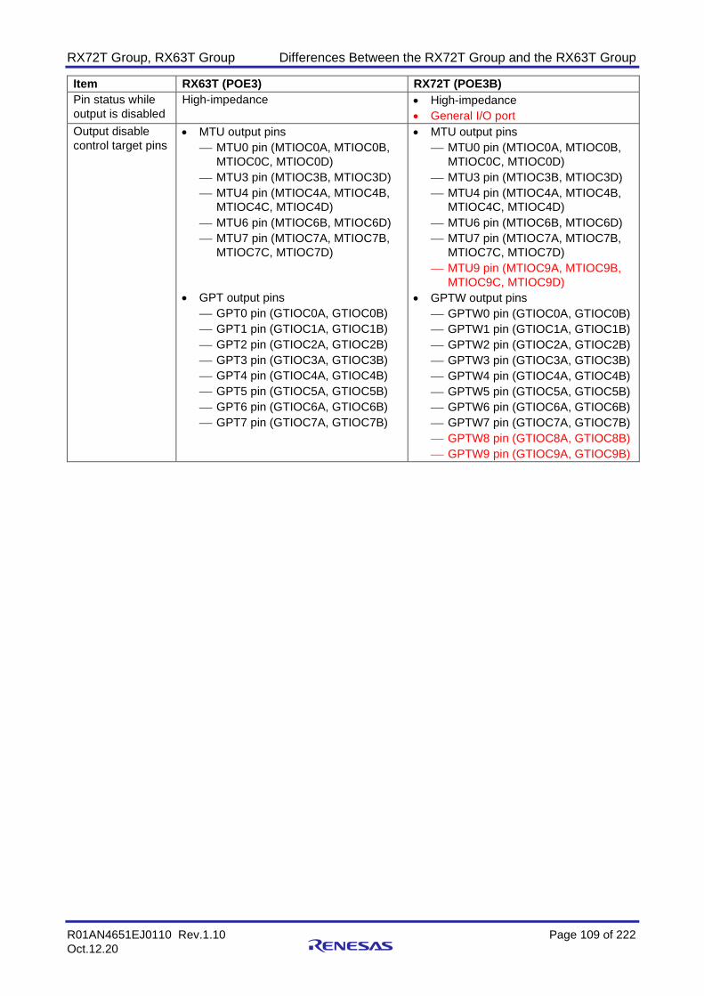
RX72T Group, RX63T Group Differences Between the RX72T Group and the RX63T Group
R01AN4651EJ0110 Rev.1.10 Page 109 of 222
Oct.12.20
Item RX63T (POE3) RX72T (POE3B)
Pin status while
output is disabled
High-impedance • High-impedance
• General I/O port
Output disable
control target pins • MTU output pins
⎯ MTU0 pin (MTIOC0A, MTIOC0B,
MTIOC0C, MTIOC0D)
⎯ MTU3 pin (MTIOC3B, MTIOC3D)
⎯ MTU4 pin (MTIOC4A, MTIOC4B,
MTIOC4C, MTIOC4D)
⎯ MTU6 pin (MTIOC6B, MTIOC6D)
⎯ MTU7 pin (MTIOC7A, MTIOC7B,
MTIOC7C, MTIOC7D)
• GPT output pins
⎯ GPT0 pin (GTIOC0A, GTIOC0B)
⎯ GPT1 pin (GTIOC1A, GTIOC1B)
⎯ GPT2 pin (GTIOC2A, GTIOC2B)
⎯ GPT3 pin (GTIOC3A, GTIOC3B)
⎯ GPT4 pin (GTIOC4A, GTIOC4B)
⎯ GPT5 pin (GTIOC5A, GTIOC5B)
⎯ GPT6 pin (GTIOC6A, GTIOC6B)
⎯ GPT7 pin (GTIOC7A, GTIOC7B)
• MTU output pins
⎯ MTU0 pin (MTIOC0A, MTIOC0B,
MTIOC0C, MTIOC0D)
⎯ MTU3 pin (MTIOC3B, MTIOC3D)
⎯ MTU4 pin (MTIOC4A, MTIOC4B,
MTIOC4C, MTIOC4D)
⎯ MTU6 pin (MTIOC6B, MTIOC6D)
⎯ MTU7 pin (MTIOC7A, MTIOC7B,
MTIOC7C, MTIOC7D)
⎯ MTU9 pin (MTIOC9A, MTIOC9B,
MTIOC9C, MTIOC9D)
• GPTW output pins
⎯ GPTW0 pin (GTIOC0A, GTIOC0B)
⎯ GPTW1 pin (GTIOC1A, GTIOC1B)
⎯ GPTW2 pin (GTIOC2A, GTIOC2B)
⎯ GPTW3 pin (GTIOC3A, GTIOC3B)
⎯ GPTW4 pin (GTIOC4A, GTIOC4B)
⎯ GPTW5 pin (GTIOC5A, GTIOC5B)
⎯ GPTW6 pin (GTIOC6A, GTIOC6B)
⎯ GPTW7 pin (GTIOC7A, GTIOC7B)
⎯ GPTW8 pin (GTIOC8A, GTIOC8B)
⎯ GPTW9 pin (GTIOC9A, GTIOC9B)

RX72T Group, RX63T Group Differences Between the RX72T Group and the RX63T Group
R01AN4651EJ0110 Rev.1.10 Page 110 of 222
Oct.12.20
Item RX63T (POE3) RX72T (POE3B)
Conditions for
generating output
disable request
• Input pin changes
When signal input occurs on pin
POE0#, POE4#, POE8#, POE10#,
POE11#, or POE12#.
• Short circuit of output pins:
Output of one of the combinations
listed below
A match (short circuit) of signal levels
lasting one or more cycles on a
combination of pins listed below
[MTU complementary PWM output pins]
⎯ MTIOC3B and MTIOC3D
⎯ MTIOC4A and MTIOC4C
⎯ MTIOC4B and MTIOC4D
⎯ MTIOC6B and MTIOC6D
⎯ MTIOC7A and MTIOC7C
⎯ MTIOC7B and MTIOC7D
[GPT output pins]
⎯ GTIOC0A and GTIOC0B
⎯ GTIOC1A and GTIOC1B
⎯ GTIOC2A and GTIOC2B
⎯ GTIOC4A and GTIOC4B
⎯ GTIOC5A and GTIOC5B
⎯ GTIOC6A and GTIOC6B
• Making of SPOER register setting
• Detection of stopped oscillation on
main clock oscillator
• Detection of output from 12-bit A/D
converter (S12ADB)
• Input pin changes
When signal input occurs on pin
POE0#, POE4#, POE8#, POE9#,
POE10#, POE11#, POE12#, POE13#,
or POE14#
• Short circuit of output pins:
Output of one of the combinations
listed below
A match (short circuit) of signal levels
lasting one or more cycles on a
combination of pins listed below
[MTU complementary PWM output pins]
⎯ MTIOC3B and MTIOC3D
⎯ MTIOC4A and MTIOC4C
⎯ MTIOC4B and MTIOC4D
⎯ MTIOC6B and MTIOC6D
⎯ MTIOC7A and MTIOC7C
⎯ MTIOC7B and MTIOC7D
[GPTW output pins]
⎯ GTIOC0A and GTIOC0B
⎯ GTIOC1A and GTIOC1B
⎯ GTIOC2A and GTIOC2B
⎯ GTIOC4A and GTIOC4B
⎯ GTIOC5A and GTIOC5B
⎯ GTIOC6A and GTIOC6B
⎯ GTIOC7A and GTIOC7B
⎯ GTIOC8A and GTIOC8B
⎯ GTIOC9A and GTIOC9B
• Making of SPOER register setting
• Detection of stopped oscillation on
main clock oscillator
• Detection of comparator C (CMPC)
output

RX72T Group, RX63T Group Differences Between the RX72T Group and the RX63T Group
R01AN4651EJ0110 Rev.1.10 Page 111 of 222
Oct.12.20
Table 2.62 Comparison of Port Output Enable 3 Registers
Register Bit RX63T (POE3) RX72T (POE3B)
ICSR1 POE0M[1:0]
(RX63T)
POE0M[3:0]
(RX72T)
POE0 mode select bits (b1, b0) POE0 mode select bits (b3 to b0)
b1 b0 b3 b0
0 0: Accepts a high-impedance
control request at the falling edge
of the POE0# pin input.
0 0 0 0: Accepts a request at the
falling edge of the POE0# pin
input.
0 1: Accepts a high-impedance
control request when the POE0#
pin input has been sampled at
low level 16 times at PCLK/8
clock pulses and all are low level.
0 0 0 1: Samples the level of the
POE0# pin input at PCLK/8,
and accepts a request when
consecutive low-level results
are detected the specified
number of times.
1 0: Accepts a high-impedance
control request when the POE0#
pin input has been sampled at
low level 16 times at PCLK/16
clock pulses and all are low level.
0 0 1 0: Samples the level of the
POE0# pin input at PCLK/16,
and accepts a request when
consecutive low-level results
are detected the specified
number of times.
1 1: Accepts a high-impedance
control request when the POE0#
pin input has been sampled at
low level 16 times at PCLK/128
clock pulses and all are low level.
0 0 1 1: Samples the level of the
POE0# pin input at
PCLK/128, and accepts a
request when consecutive
low-level results are detected
the specified number of
times.
0 1 0 0: Samples the level of the
POE0# pin input at PCLK,
and accepts a request when
consecutive low-level results
are detected the specified
number of times.
0 1 0 1: Samples the level of the
POE0# pin input at PCLK/2,
and accepts a request when
consecutive low-level results
are detected the specified
number of times.
0 1 1 0: Samples the level of the
POE0# pin input at PCLK/4,
and accepts a request when
consecutive low-level results
are detected the specified
number of times.
Settings other than the above are
prohibited.
POE0M2[3:0] ⎯ POE0 sampling count select bits

RX72T Group, RX63T Group Differences Between the RX72T Group and the RX63T Group
R01AN4651EJ0110 Rev.1.10 Page 112 of 222
Oct.12.20
Register Bit RX63T (POE3) RX72T (POE3B)
ICSR1 POE0F POE0 flag
[Setting condition]
When the input set by the
POE0M[1:0] bits occurs on the
POE0# pin [Clearing condition]
When 0 is written to the POE0F flag
after reading it as 1
When low-level sampling is specified
by the POE0M[1:0] bits, a high level
signal needs to be input on the
POE0# pin to write 0 to this flag.
POE0 flag
[Setting condition]
When the input set by the
POE0M[3:0] and POE0M2[3:0] bits
occurs on the POE0# pin [Clearing condition]
When 0 is written to the POE0F flag
after reading it as 1
When low-level sampling is specified
by the POE0M[3:0] bits, a high level
signal needs to be input on the
POE0# pin to write 0 to this flag.
ICSR2 POE4M[1:0]
(RX63T)
POE4M[3:0]
(RX72T)
POE4 mode select bits (b1, b0)
b1 b0
0 0: Accepts a high-impedance
control request at the falling edge
of the POE4# pin input.
POE4 mode select bits (b3 to b0)
b3 b0
0 0 0 0: Accepts a request at the
falling edge of the POE4# pin
input.
0 1: Accepts a high-impedance
control request when the POE4#
pin input has been sampled at
low level 16 times at PCLK/8
clock pulses and all are low level.
0 0 0 1: Samples the level of the
POE4# pin input at PCLK/8,
and accepts a request when
consecutive low-level results
are detected the specified
number of times.
1 0: Accepts a high-impedance
control request when the POE4#
pin input has been sampled at
low level 16 times at PCLK/16
clock pulses and all are low level.
0 0 1 0: Samples the level of the
POE4# pin input at PCLK/16,
and accepts a request when
consecutive low-level results
are detected the specified
number of times.
1 1: Accepts a high-impedance
control request when the POE4#
pin input has been sampled at
low level 16 times at PCLK/128
clock pulses and all are low level.
0 0 1 1: Samples the level of the
POE4# pin input at
PCLK/128, and accepts a
request when consecutive
low-level results are detected
the specified number of
times.

RX72T Group, RX63T Group Differences Between the RX72T Group and the RX63T Group
R01AN4651EJ0110 Rev.1.10 Page 113 of 222
Oct.12.20
Register Bit RX63T (POE3) RX72T (POE3B)
ICSR2 POE4M[1:0]
(RX63T)
POE4M[3:0]
(RX72T)
0 1 0 0: Samples the level of the
POE4# pin input at PCLK,
and accepts a request when
consecutive low-level results
are detected the specified
number of times.
0 1 0 1: Samples the level of the
POE4# pin input at PCLK/2,
and accepts a request when
consecutive low-level results
are detected the specified
number of times.
0 1 1 0: Samples the level of the
POE4# pin input at PCLK/4,
and accepts a request when
consecutive low-level results
are detected the specified
number of times.
Settings other than the above are
prohibited.
POE4M2[3:0] ⎯ POE4 sampling count select bits
POE4F POE4 flag
[Setting condition]
When the input set by the
POE4M[1:0] bits occurs on the
POE4# pin [Clearing condition]
When 0 is written to the POE4F flag
after reading it as 1
When low-level sampling is specified
by the POE4M[1:0] bits, a high level
signal needs to be input on the
POE4# pin to write 0 to this flag.
POE4 flag
[Setting condition]
When the input set by the
POE4M[3:0] and POE4M2[3:0] bits
occurs on the POE4# pin [Clearing condition]
When 0 is written to the POE4F flag
after reading it as 1
When low-level sampling is specified
by the POE4M[3:0] bits, a high level
signal needs to be input on the
POE4# pin to write 0 to this flag.
ICSR3 POE8M[1:0]
(RX63T)
POE8M[3:0]
(RX72T)
POE8 mode select bits (b1, b0)
b1 b0
0 0: Accepts a high-impedance
control request at the falling edge
of the POE8# pin input.
POE8 mode select bits (b3 to b0)
b3 b0
0 0 0 0: Accepts a request at the
falling edge of the POE8# pin
input.
0 1: Accepts a high-impedance
control request when the POE8#
pin input has been sampled at
low level 16 times at PCLK/8
clock pulses and all are low level.
0 0 0 1: Samples the level of the
POE8# pin input at PCLK/8,
and accepts a request when
consecutive low-level results
are detected the specified
number of times.
1 0: Accepts a high-impedance
control request when the POE8#
pin input has been sampled at
low level 16 times at PCLK/16
clock pulses and all are low level.
0 0 1 0: Samples the level of the
POE8# pin input at PCLK/16,
and accepts a request when
consecutive low-level results
are detected the specified
number of times.

RX72T Group, RX63T Group Differences Between the RX72T Group and the RX63T Group
R01AN4651EJ0110 Rev.1.10 Page 114 of 222
Oct.12.20
Register Bit RX63T (POE3) RX72T (POE3B)
ICSR3 POE8M[1:0]
(RX63T)
POE8M[3:0]
(RX72T)
1 1: Accepts a high-impedance
control request when the POE8#
pin input has been sampled at
low level 16 times at PCLK/128
clock pulses and all are low level.
0 0 1 1: Samples the level of the
POE8# pin input at
PCLK/128, and accepts a
request when consecutive
low-level results are detected
the specified number of
times.
0 1 0 0: Samples the level of the
POE8# pin input at PCLK,
and accepts a request when
consecutive low-level results
are detected the specified
number of times.
0 1 0 1: Samples the level of the
POE8# pin input at PCLK/2,
and accepts a request when
consecutive low-level results
are detected the specified
number of times.
0 1 1 0: Samples the level of the
POE8# pin input at PCLK/4,
and accepts a request when
consecutive low-level results
are detected the specified
number of times.
Settings other than the above are
prohibited.
POE8M2[3:0] ⎯ POE8 sampling count select bits
POE8F POE8 flag
[Setting condition]
When the input set by the
POE8M[1:0] bits occurs on the
POE8# pin [Clearing condition]
When 0 is written to the POE8F flag
after reading it as 1
When low-level sampling is specified
by the POE8M[1:0] bits, a high level
signal needs to be input on the
POE8# pin to write 0 to this flag.
POE8 flag
[Setting condition]
When the input set by the
POE8M[3:0] and POE8M2[3:0] bits
occurs on the POE8# pin [Clearing condition]
When 0 is written to the POE8F flag
after reading it as 1
When low-level sampling is specified
by the POE8M[3:0] bits, a high level
signal needs to be input on the
POE8# pin to write 0 to this flag.
ICSR4 POE10M[1:0]
(RX63T)
POE10M[3:0]
(RX72T)
POE10 mode select bits (b1, b0)
b1 b0
0 0: Accepts a high-impedance
control request at the falling edge
of the POE10# pin input.
POE10 mode select bits (b3 to b0)
b3 b0
0 0 0 0: Accepts a request at the
falling edge of the POE10#
pin input.
0 1: Accepts a high-impedance
control request when the
POE10# pin input has been
sampled at low level 16 times at
PCLK/8 clock pulses and all are
low level.
0 0 0 1: Samples the level of the
POE10# pin input at PCLK/8,
and accepts a request when
consecutive low-level results
are detected the specified
number of times.

RX72T Group, RX63T Group Differences Between the RX72T Group and the RX63T Group
R01AN4651EJ0110 Rev.1.10 Page 115 of 222
Oct.12.20
Register Bit RX63T (POE3) RX72T (POE3B)
ICSR4 POE10M[1:0]
(RX63T)
POE10M[3:0]
(RX72T)
1 0: Accepts a high-impedance
control request when the
POE10# pin input has been
sampled at low level 16 times at
PCLK/16 clock pulses and all are
low level.
0 0 1 0: Samples the level of the
POE10# pin input at
PCLK/16, and accepts a
request when consecutive
low-level results are detected
the specified number of
times.
1 1: Accepts a high-impedance
control request when the
POE10# pin input has been
sampled at low level 16 times at
PCLK/128 clock pulses and all
are low level.
0 0 1 1: Samples the level of the
POE10# pin input at
PCLK/128, and accepts a
request when consecutive
low-level results are detected
the specified number of
times.
0 1 0 0: Samples the level of the
POE10# pin input at PCLK,
and accepts a request when
consecutive low-level results
are detected the specified
number of times.
0 1 0 1: Samples the level of the
POE10# pin input at PCLK/2,
and accepts a request when
consecutive low-level results
are detected the specified
number of times.
0 1 1 0: Samples the level of the
POE10# pin input at PCLK/4,
and accepts a request when
consecutive low-level results
are detected the specified
number of times.
Settings other than the above are
prohibited.
POE10M2[3:0] ⎯ POE10 sampling count select bits
POE10F POE10 flag
[Setting condition]
When the input set by the
POE10M[1:0] bits occurs on the
POE10# pin [Clearing condition]
When 0 is written to the POE10F flag
after reading it as 1
When low-level sampling is specified
by the POE10M[1:0] bits, a high level
signal needs to be input on the
POE10# pin to write 0 to this flag.
POE10 flag
[Setting condition]
When the input set by the
POE10M[3:0] and POE10M2[3:0] bits
occurs on the POE10# pin [Clearing condition]
When 0 is written to the POE10F flag
after reading it as 1
When low-level sampling is specified
by the POE10M[3:0] bits, a high level
signal needs to be input on the
POE10# pin to write 0 to this flag.

RX72T Group, RX63T Group Differences Between the RX72T Group and the RX63T Group
R01AN4651EJ0110 Rev.1.10 Page 116 of 222
Oct.12.20
Register Bit RX63T (POE3) RX72T (POE3B)
ICSR5 POE11M[1:0]
(RX63T)
POE11M[3:0]
(RX72T)
POE11 mode select bits (b1, b0)
b1 b0
0 0: Accepts a high-impedance
control request at the falling edge
of the POE11# pin input.
POE11 mode select bits (b3 to b0)
b3 b0
0 0 0 0: Accepts a request at the
falling edge of the POE11#
pin input.
0 1: Accepts a high-impedance
control request when the
POE11# pin input has been
sampled at low level 16 times at
PCLK/8 clock pulses and all are
low level.
0 0 0 1: Samples the level of the
POE11# pin input at PCLK/8,
and accepts a request when
consecutive low-level results
are detected the specified
number of times.
1 0: Accepts a high-impedance
control request when the
POE11# pin input has been
sampled at low level 16 times at
PCLK/16 clock pulses and all are
low level.
0 0 1 0: Samples the level of the
POE11# pin input at
PCLK/16, and accepts a
request when consecutive
low-level results are detected
the specified number of
times.
1 1: Accepts a high-impedance
control request when the
POE11# pin input has been
sampled at low level 16 times at
PCLK/128 clock pulses and all
are low level.
0 0 1 1: Samples the level of the
POE11# pin input at
PCLK/128, and accepts a
request when consecutive
low-level results are detected
the specified number of
times.
0 1 0 0: Samples the level of the
POE11# pin input at PCLK,
and accepts a request when
consecutive low-level results
are detected the specified
number of times.
0 1 0 1: Samples the level of the
POE11# pin input at PCLK/2,
and accepts a request when
consecutive low-level results
are detected the specified
number of times.
0 1 1 0: Samples the level of the
POE11# pin input at PCLK/4,
and accepts a request when
consecutive low-level results
are detected the specified
number of times.
Settings other than the above are
prohibited.
POE11M2[3:0] ⎯ POE11 sampling count select bits

RX72T Group, RX63T Group Differences Between the RX72T Group and the RX63T Group
R01AN4651EJ0110 Rev.1.10 Page 117 of 222
Oct.12.20
Register Bit RX63T (POE3) RX72T (POE3B)
ICSR5 POE11F POE11 flag
[Setting condition]
When the input set by the
POE11M[1:0] bits occurs on the
POE11# pin [Clearing condition]
When 0 is written to the POE11F flag
after reading it as 1
When low-level sampling is specified
by the POE11M[1:0] bits, a high level
signal needs to be input on the
POE11# pin to write 0 to this flag.
POE11 flag
[Setting condition]
When the input set by the
POE11M[3:0] and POE11M2[3:0] bits
occurs on the POE11# pin [Clearing condition]
When 0 is written to the POE11F flag
after reading it as 1
When low-level sampling is specified
by the POE11M[3:0] bits, a high level
signal needs to be input on the
POE11# pin to write 0 to this flag.
ICSR7 POE12M[1:0]
(RX63T)
POE12M[3:0]
(RX72T)
POE12 mode select bits (b1, b0)
b1 b0
0 0: Accepts a high-impedance
control request at the falling edge
of the POE12# pin input.
POE12 mode select bits (b3 to b0)
b3 b0
0 0 0 0: Accepts a request at the
falling edge of the POE12#
pin input.
0 1: Accepts a high-impedance
control request when the
POE12# pin input has been
sampled at low level 16 times at
PCLK/8 clock pulses and all are
low level.
0 0 0 1: Samples the level of the
POE12# pin input at PCLK/8,
and accepts a request when
consecutive low-level results
are detected the specified
number of times.
1 0: Accepts a high-impedance
control request when the
POE12# pin input has been
sampled at low level 16 times at
PCLK/16 clock pulses and all are
low level.
0 0 1 0: Samples the level of the
POE12# pin input at
PCLK/16, and accepts a
request when consecutive
low-level results are detected
the specified number of
times.
1 1: Accepts a high-impedance
control request when the
POE12# pin input has been
sampled at low level 16 times at
PCLK/128 clock pulses and all
are low level.
0 0 1 1: Samples the level of the
POE12# pin input at
PCLK/128, and accepts a
request when consecutive
low-level results are detected
the specified number of
times.

RX72T Group, RX63T Group Differences Between the RX72T Group and the RX63T Group
R01AN4651EJ0110 Rev.1.10 Page 118 of 222
Oct.12.20
Register Bit RX63T (POE3) RX72T (POE3B)
ICSR7 POE12M[1:0]
(RX63T)
POE12M[3:0]
(RX72T)
0 1 0 0: Samples the level of the
POE12# pin input at PCLK,
and accepts a request when
consecutive low-level results
are detected the specified
number of times.
0 1 0 1: Samples the level of the
POE12# pin input at PCLK/2,
and accepts a request when
consecutive low-level results
are detected the specified
number of times.
0 1 1 0: Samples the level of the
POE12# pin input at PCLK/4,
and accepts a request when
consecutive low-level results
are detected the specified
number of times.
Settings other than the above are
prohibited.
POE12M2[3:0] ⎯ POE12 sampling count select bits
POE12F POE12 flag
[Setting condition]
When the input set by the
POE12M[1:0] bits occurs on the
POE12# pin [Clearing condition]
When 0 is written to the POE12F flag
after reading it as 1
When low-level sampling is specified
by the POE12M[1:0] bits, a high level
signal needs to be input on the
POE12# pin to write 0 to this flag.
POE12 flag
[Setting condition]
When the input set by the
POE12M[3:0] and POE12M2[3:0] bits
occurs on the POE12# pin [Clearing condition]
When 0 is written to the POE12F flag
after reading it as 1
When low-level sampling is specified
by the POE12M[3:0] bits, a high level
signal needs to be input on the
POE12# pin to write 0 to this flag.
ICSR8 ⎯ ⎯ Input level control/status register 8
ICSR9 ⎯ ⎯ Input level control/status register 9
ICSR10 ⎯ ⎯ Input level control/status register 10
M0SELR1 ⎯ ⎯ MTU0 pin select register 1
M0SELR2 ⎯ ⎯ MTU0 pin select register 2
M3SELR ⎯ ⎯ MTU3 pin select register
M4SELR1 ⎯ ⎯ MTU4 pin select register 1
M4SELR2 ⎯ ⎯ MTU4 pin select register 2
M6SELR ⎯ ⎯ MTU6 pin select register
M7SELR1 ⎯ ⎯ MTU7 pin select register 1
M7SELR2 ⎯ ⎯ MTU7 pin select register 2
M9SELR1 ⎯ ⎯ MTU9 pin select register 1
M9SELR2 ⎯ ⎯ MTU9 pin select register 2
G0SELR ⎯ ⎯ GPTW0 pin select register
G1SELR ⎯ ⎯ GPTW1 pin select register
G2SELR ⎯ ⎯ GPTW2 pin select register
G3SELR ⎯ ⎯ GPTW3 pin select register
G4SELR ⎯ ⎯ GPTW4 pin select register

RX72T Group, RX63T Group Differences Between the RX72T Group and the RX63T Group
R01AN4651EJ0110 Rev.1.10 Page 119 of 222
Oct.12.20
Register Bit RX63T (POE3) RX72T (POE3B)
G5SELR ⎯ ⎯ GPTW5 pin select register
G6SELR ⎯ ⎯ GPTW6 pin select register
G7SELR ⎯ ⎯ GPTW7 pin select register
G8SELR ⎯ ⎯ GPTW8 pin select register
G9SELR ⎯ ⎯ GPTW9 pin select register
ALR1 OLSG0A MTIOC3B/GTIOC0A active level
setting bit
MTIOC3B pin active level setting bit
OLSG0B MTIOC3D/GTIOC0B active level
setting bit
MTIOC3D pin active level setting bit
OLSG1A MTIOC4A/GTIOC1A active level
setting bit
MTIOC4A pin active level setting bit
OLSG1B MTIOC4C/GTIOC1B active level
setting bit
MTIOC4C pin active level setting bit
OLSG2A MTIOC4B/GTIOC2A active level
setting bit
MTIOC4B pin active level setting bit
OLSG2B MTIOC4D/GTIOC2B active level
setting bit
MTIOC4D pin active level setting bit
MTUCHSEL MTU output active level channel
setting bit
⎯
ALR2 OLSG4A MTIOC6B/GTIOC4A active level
setting bit
MTIOC6B active level setting bit
OLSG4B MTIOC6D/GTIOC4B active level
setting bit
MTIOC6D active level setting bit
OLSG5A MTIOC7A/GTIOC5A active level
setting bit
MTIOC7A active level setting bit
OLSG5B MTIOC7C/GTIOC5B active level
setting bit
MTIOC7C active level setting bit
OLSG6A MTIOC7B/GTIOC6A active level
setting bit
MTIOC7B active level setting bit
OLSG6B MTIOC7D/GTIOC6B active level
setting bit
MTIOC7D active level setting bit
ALR3 ⎯ ⎯ Active level register 3
ALR4 ⎯ ⎯ Active level register 4
ALR5 ⎯ ⎯ Active level register 5
SPOER MTUCH34HIZ*1 MTU3 and MTU4 output high-
impedance enable bit
MTU3 and MTU4 pin output disable
bit
MTUCH67HIZ*1 MTU6 and MTU7 output high-
impedance enable bit
MTU6 and MTU7 pin output disable
bit
GPT01HIZ GPT0 and GPT1 output high-
impedance enable bit
GPTW0 and GPTW1 pin output
disable bit
GPT23HIZ GPT2 and GPT3 output high-
impedance enable bit
GPTW2 and GPTW3 pin output
disable bit
MTUCH9HIZ ⎯ MTU9 pin output disable bit
GPT02HIZ ⎯ GPTW0 to GPTW2 pin output disable
bit
GPT46HIZ ⎯ GPTW4 to GPTW6 pin output disable
bit
GPT67HIZ*1 GPT6 and GPT7 output high-
impedance enable bit
⎯
GPT79HIZ ⎯ GPTW7 to GPTW9 pin output disable
bit

RX72T Group, RX63T Group Differences Between the RX72T Group and the RX63T Group
R01AN4651EJ0110 Rev.1.10 Page 120 of 222
Oct.12.20
Register Bit RX63T (POE3) RX72T (POE3B)
POECR2 MTU7BDZE*1 MTU CH7BD high-impedance enable
bit
MTIOC7B/MTIOC7D pin high-
impedance enable bit
MTU7ACZE*1 MTU CH7AC high-impedance enable
bit
MTIOC7A/MTIOC7C pin high-
impedance enable bit
MTU6BDZE*1 MTU CH6BD high-impedance enable
bit
MTIOC6B/MTIOC6D pin high-
impedance enable bit
MTU4BDZE*1 MTU CH4BD high-impedance enable
bit
MTIOC4B/MTIOC4D pin high-
impedance enable bit
MTU4ACZE*1 MTU CH4AC high-impedance enable
bit
MTIOC4A/MTIOC4C pin high-
impedance enable bit
MTU3BDZE*1 MTU CH3BD high-impedance enable
bit
MTIOC3B/MTIOC3D pin high-
impedance enable bit
POECR3 ⎯ Port output enable control register 3 Port output enable control register 3
Initial values after a reset are different.
GPT2ABZE
GPT CH2AB high-impedance enable
bit (b8)
GTIOC2A/GTIOC2B pin high-
impedance enable bit (b2)
GPT3ABZE GPT CH3AB high-impedance enable
bit (b9)
GTIOC3A/GTIOC3B pin high-
impedance enable bit (b3)
GPT4ABZE to
GPT9ABZE
⎯ GTIOC4A/GTIOC4B to
GTIOC9A/GTIOC9B pin high-
impedance enable bit
POECR4 CMADDMT34ZE*1 MTU CH34 high-impedance CFLAG
add bit
MTU3 and MTU4 output disabling
condition CFLAG add bit
IC1ADDMT34ZE ⎯ MTU3 and MTU4 output disabling
condition POE0F add bit
IC2ADDMT34ZE*1 MTU CH34 high-impedance POE4F
add bit
MTU3 and MTU4 output disabling
condition POE4F add bit
IC3ADDMT34ZE*1 MTU CH34 high-impedance POE8F
add bit
MTU3 and MTU4 output disabling
condition POE8F add bit
IC4ADDMT34ZE*1 MTU CH34 high-impedance POE10F
add bit
MTU3 and MTU4 output disabling
condition POE10F add bit
IC5ADDMT34ZE*1 MTU CH34 high-impedance POE11F
add bit
MTU3 and MTU4 output disabling
condition POE11F add bit
IC6ADDMT34ZE*1 MTU CH34 high-impedance POE12F
add bit
MTU3 and MTU4 output disabling
condition POE12F add bit
IC8ADDMT34ZE ⎯ MTU3 and MTU4 output disabling
condition POE9F add bit
IC9ADDMT34ZE ⎯ MTU3 and MTU4 output disabling
condition POE13F add bit
IC10ADDMT34ZE ⎯ MTU3 and MTU4 output disabling
condition POE14F add bit
CMADOMT67ZE MTU CH67 high-impedance CFLAG
add bit
⎯
IC1ADDMT67ZE MTU CH67 high-impedance POE0F
add bit
⎯
IC3ADDMT67ZE MTU CH67 high-impedance POE8F
add bit
⎯
IC4ADDMT67ZE MTU CH67 high-impedance POE10F
add bit
⎯
IC5ADDMT67ZE MTU CH67 high-impedance POE11F
add bit
⎯
IC6ADDMT67ZE MTU CH67 high-impedance POE12F
add bit
⎯

RX72T Group, RX63T Group Differences Between the RX72T Group and the RX63T Group
R01AN4651EJ0110 Rev.1.10 Page 121 of 222
Oct.12.20
Register Bit RX63T (POE3) RX72T (POE3B)
POECR4B ⎯ ⎯ Port output enable control register 4B
POECR5 IC3ADDMT0ZE ⎯ MTU0 output disabling condition
POE8F add bit
IC8ADDMT0ZE ⎯ MTU0 output disabling condition
POE9F add bit
IC9ADDMT0ZE ⎯ MTU0 output disabling condition
POE13F add bit
IC10ADDMT0ZE ⎯ MTU0 output disabling condition
POE14F add bit
POECR6 IC4ADDGPT01ZE ⎯ GPTW0 and GPTW1 output disabling
condition POE10F add bit
IC8ADDGPT01ZE ⎯ GPTW0 and GPTW1 output disabling
condition POE9F add bit
IC9ADDGPT01ZE ⎯ GPTW0 and GPTW1 output disabling
condition POE13F add bit
IC10ADDGPT01ZE ⎯ GPTW0 and GPTW1 output disabling
condition POE14F add bit
CMADDGPT23ZE GPT CH23 high-impedance CFLAG
add bit
⎯
IC1ADDGPT23ZE GPT CH23 high-impedance POE0F
add bit
⎯
IC2ADDGPT23ZE GPT CH23 high-impedance POE4F
add bit
⎯
IC3ADDGPT23ZE GPT CH23 high-impedance POE8F
add bit
⎯
IC4ADDGPT23ZE GPT CH23 high-impedance POE10F
add bit
⎯
IC6ADDGPT23ZE GPT CH23 high-impedance POE12F
add bit
⎯
POECR6B ⎯ ⎯ Port output enable control register 6B
POECR7 MTU9AZE ⎯ MTIOC9A pin high-impedance enable
bit
MTU9BZE ⎯ MTIOC9B pin high-impedance enable
bit
MTU9CZE ⎯ MTIOC9C pin high-impedance enable
bit
MTU9DZE ⎯ MTIOC9D pin high-impedance enable
bit
GPT6ABZE GPT6ABZE high-impedance enable
bit
⎯
GPT7ABZE GPT7ABZE high-impedance enable
bit
⎯
POECR8 CMADDMT9ZE ⎯ MTU9 output disabling condition
CFLAG add bit
IC1ADDMT9ZE ⎯ MTU9 output disabling condition
POE0F add bit
IC2ADDMT9ZE ⎯ MTU9 output disabling condition
POE4F add bit
IC3ADDMT9ZE ⎯ MTU9 output disabling condition
POE8F add bit
IC4ADDMT9ZE ⎯ MTU9 output disabling condition
POE10F add bit

RX72T Group, RX63T Group Differences Between the RX72T Group and the RX63T Group
R01AN4651EJ0110 Rev.1.10 Page 122 of 222
Oct.12.20
Register Bit RX63T (POE3) RX72T (POE3B)
POECR8 IC5ADDMT9ZE ⎯ MTU9 output disabling condition
POE11F add bit
IC6ADDMT9ZE ⎯ MTU9 output disabling condition
POE12F add bit
IC8ADDMT9ZE ⎯ MTU9 output disabling condition
POE9F add bit
IC9ADDMT9ZE ⎯ MTU9 output disabling condition
POE13F add bit
IC10ADDMT9ZE ⎯ MTU9 output disabling condition
POE14F add bit
CMADDGPT67ZE GPT CH67 high-impedance CFLAG
add bit
⎯
IC1ADDGPT67ZE GPT CH67 high-impedance POE0F
add bit
⎯
IC2ADDGPT67ZE GPT CH67 high-impedance POE4F
add bit
⎯
IC3ADDGPT67ZE GPT CH67 high-impedance POE8F
add bit
⎯
IC4ADDGPT67ZE GPT CH67 high-impedance POE10F
add bit
⎯
IC5ADDGPT67ZE GPT CH67 high-impedance POE11F
add bit
⎯
POECR9 ⎯ ⎯ Port output enable control register 9
POECR10 ⎯ ⎯ Port output enable control register 10
POECR11 ⎯ ⎯ Port output enable control register 11
PMMCR0 ⎯ ⎯ Port mode mask control register 0
PMMCR1 ⎯ ⎯ Port mode mask control register 1
PMMCR2 ⎯ ⎯ Port mode mask control register 2
PMMCR3 ⎯ ⎯ Port mode mask control register 3

RX72T Group, RX63T Group Differences Between the RX72T Group and the RX63T Group
R01AN4651EJ0110 Rev.1.10 Page 123 of 222
Oct.12.20
Register Bit RX63T (POE3) RX72T (POE3B)
OCSR1 OSF1 Output short flag 1
[144-, 120-, 112-, and 100-pin
versions]
This flag indicates that one or more of
the three pairs of two-phase outputs
among MTU complementary PWM
output pins P71 to P76 (pins MTU3
and MTU4) or GPT output pins
(GPT0 to GPT2) to be compared has
simultaneously been at active level.
[64- and 48-pin versions]
This flag indicates that one or more of
the three pairs of two-phase outputs
among MTU complementary PWM
output pins P71 to P76 (pins MTU3
and MTU4 or MTU6 and MTU7) or
GPT output pins (GPT0 to GPT2) to
be compared has simultaneously
been at active level.
Output short flag 1
This flag indicates that one or more of
the three pairs of two-phase outputs
among MTU complementary PWM
output pins (pins MTU3 and MTU4)
has simultaneously been at active
level. However, if output disabling
control for the corresponding pins is
not enabled, this flag is not set to 1.
[Setting condition]
When any one of the three pairs of
two-phase outputs has
simultaneously been at active level
[Setting condition]
• When pins MTIOC3B and
MTIOC3D simultaneously go to
the active level for at least one
cycle of PCLK while the value of
the POECR2.MTU3BDZE bit, or
at least one of bits
PMMCR1.MTU3BME and
PMMCR1.MTU3DME, is 1.
• When pins MTIOC4A and
MTIOC4C simultaneously go to
the active level for at least one
cycle of PCLK while the value of
the POECR2.MTU4ACZE bit, or
at least one of bits
PMMCR1.MTU4AME and
PMMCR1.MTU4CME, is 1.
• When pins MTIOC4B and
MTIOC4D simultaneously go to
the active level for at least one
cycle of PCLK while the value of
the POECR2.MTU4BDZE bit, or
at least one of bits
PMMCR1.MTU4BME and
PMMCR1.MTU4DME, is 1.
[Clearing condition]
When 0 is written to the OSF1 flag
after reading it as 1
The output from the MTU
complementary PWM output pins or
GPT output pins must be at the
inactive level when 0 is written to the
flag.
[Clearing condition]
When 0 is written to the OSF1 flag
after reading it as 1
To write 0 to this flag, the output on
the MTU complementary PWM output
pins must be at the inactive level.

RX72T Group, RX63T Group Differences Between the RX72T Group and the RX63T Group
R01AN4651EJ0110 Rev.1.10 Page 124 of 222
Oct.12.20
Register Bit RX63T (POE3) RX72T (POE3B)
OCSR2 OSF2 Output short flag 2
This flag indicates that one or more of
the three pairs of two-phase outputs
among MTU complementary PWM
output pins (pins MTU6 and MTU7) or
GPT output pins (GPT4 to GPT6) has
simultaneously been at active level.
Output short flag 2
This flag indicates that one or more of
the three pairs of two-phase outputs
among MTU complementary PWM
output pins (pins MTU6 and MTU7)
has simultaneously been at active
level. However, if output disabling
control for the corresponding pins is
not enabled, this flag is not set to 1.
[Setting condition]
When any one of the three pairs of
two-phase outputs has
simultaneously been at active level
[Setting condition]
• When pins MTIOC6B and
MTIOC6D simultaneously go to
the active level for at least one
cycle of PCLK while the value of
the POECR2.MTU6BDZE bit, or
at least one of bits
PMMCR1.MTU6BME and
PMMCR1.MTU6DME, is 1.
• When pins MTIOC7A and
MTIOC7C simultaneously go to
the active level for at least one
cycle of PCLK while the value of
the POECR2.MTU7ACZE bit, or
at least one of bits
PMMCR1.MTU7AME and
PMMCR1.MTU7CME, is 1.
• When pins MTIOC7B and
MTIOC7D simultaneously go to
the active level for at least one
cycle of PCLK while the value of
the POECR2.MTU7BDZE bit, or
at least one of bits
PMMCR1.MTU7BME and
PMMCR1.MTU7DME, is 1.
[Clearing condition]
By writing 0 to OSF2 after reading
OSF2 = 1
The output from the MTU
complementary PWM output pins or
GPT output pins must be at the
inactive level when 0 is written to the
flag.
[Clearing condition]
By writing 0 to OSF2 after reading
OSF2 = 1
To write 0 to this flag, the output on
the MTU complementary PWM output
pins must be at the inactive level.
OCSR3 ⎯ ⎯ Output level control/status register 3
OCSR4 ⎯ ⎯ Output level control/status register 4
OCSR5 ⎯ ⎯ Output level control/status register 5
POECMPFR ⎯ ⎯ Port output enable comparator output
detection flag register
POECMPSEL ⎯ ⎯ Port output enable comparator
request select register
POECMPEXm ⎯ ⎯ Port output enable comparator
request extended selection register m
(m = 0 to 8)
Note: 1. The GPT and MTU pins are controlled by this register on the RX63T, but the GPT and MTU pins
are controlled by separate registers on the RX72T.

RX72T Group, RX63T Group Differences Between the RX72T Group and the RX63T Group
R01AN4651EJ0110 Rev.1.10 Page 125 of 222
Oct.12.20
2.20 General PWM Timer
Table 2.88 is a comparative overview of the general PWM timers, Table 2.89 is a comparison of general PWM timer registers, and Table 2.90 is a comparative listing of GTIOA and GTIOB bit settings.
Table 2.63 Comparative Overview of General PWM Timer
Item RX63T (GPT) RX72T (GPTW)
Functions • 16 bits 8 channels
• Up-count or down-count
operation (saw waves) or
up/down-count operation
(triangle waves) for each
counter
• Independently selectable clock
source for each channel
• Two input/output pins per
channel
• Two output compare/input
capture registers per channel
• For each pair of output
compare/input capture registers
for each channel, four registers
are provided as buffer registers
and are capable of operating as
compare registers when
buffering is not in use.
• During output compare
operation, buffer switching can
be at peaks or troughs,
enabling the generation of
laterally asymmetric PWM
waveforms.
• Registers for setting up frame
cycles in each channel (with
capability for generating
interrupts at overflow or
underflow)
• Ability to synchronize operation
with any of several counters
• Synchronized operation modes
(synchronized, or displaced by
desired times for phase
shifting)
• Generation of dead time during
PWM operation
• 32 bits 10 channels
• Up-count or down-count
operation (saw waves) or
up/down-count operation
(triangle waves) for each
counter
• Independently selectable clock
source for each channel
• Two input/output pins per
channel
• Two output compare/input
capture registers per channel
• For each pair of output
compare/input capture registers
for each channel, four registers
are provided as buffer registers
and are capable of operating as
compare registers when
buffering is not in use.
• During output compare
operation, buffer switching can
be at peaks or troughs,
enabling the generation of
laterally asymmetric PWM
waveforms.
• Registers for setting up frame
cycles in each channel (with
capability for generating
interrupts at overflow or
underflow)
• Simultaneous start, stop, and
clearing of desired channel
counters
• Synchronized operation modes
(synchronized, or displaced by
desired times for phase
shifting)
• Generation of dead time during
PWM operation
• Count start, count stop, counter
clearing, up-counting, down-
counting, or input capture by up
to eight ELC events based on
the ELC settings
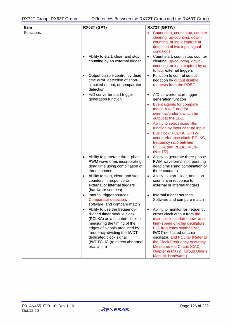
RX72T Group, RX63T Group Differences Between the RX72T Group and the RX63T Group
R01AN4651EJ0110 Rev.1.10 Page 126 of 222
Oct.12.20
Item RX63T (GPT) RX72T (GPTW)
Functions
• Ability to start, clear, and stop
counting by an external trigger
• Output disable control by dead
time error, detection of short-
circuited output, or comparator-
detection
• A/D converter start trigger
generation function
• Count start, count stop, counter
clearing, up-counting, down-
counting, or input capture at
detection of two input signal
conditions
• Count start, count stop, counter
clearing, up-counting, down-
counting, or input capture by up
to four external triggers
• Function to control output
negation by output disable
requests from the POEG
• A/D converter start trigger
generation function
• Event signals for compare
match A to F and for
overflow/underflow can be
output to the ELC.
• Ability to select noise filter
function by input capture input
• Bus clock: PCLKA, GPTW
count reference clock: PCLKC,
frequency ratio between
PCLKA and PCLKC = 1:N
(N = 1/2)
• Ability to generate three-phase
PWM waveforms incorporating
dead time using combination of
three counters
• Ability to start, clear, and stop
counters in response to
external or internal triggers
(hardware sources)
• Internal trigger sources:
Comparator detection,
software, and compare match
• Ability to use the frequency-
divided timer module clock
(PCLKA) as a counter clock for
measuring the timing of the
edges of signals produced by
frequency-dividing the IWDT-
dedicated clock signal
(IWDTCLK) (to detect abnormal
oscillation)
• Ability to generate three-phase
PWM waveforms incorporating
dead time using combination of
three counters
• Ability to start, clear, and stop
counters in response to
external or internal triggers
• Internal trigger sources:
Software and compare match
• Ability to monitor for frequency
errors clock output from the
main clock oscillator, low- and
high-speed on-chip oscillators,
PLL frequency synthesizer,
IWDT-dedicated on-chip
oscillator, and PCLKB (Refer to
the Clock Frequency Accuracy
Measurement Circuit (CAC)
chapter in RX72T Group User’s
Manual: Hardware.)

RX72T Group, RX63T Group Differences Between the RX72T Group and the RX63T Group
R01AN4651EJ0110 Rev.1.10 Page 127 of 222
Oct.12.20
Item RX63T (GPT) RX72T (GPTW)
Functions • Ability to generate three-phase
Ability to control rise and fall
timing of two PWM output pins
on channels 0 to 3 with an
accuracy of up to 1/32 times
the period of the system clock
(ICLK) (PWM delay generation
function)
• Ability to adjust rise/fall timing
of PWM waveforms with
resolution of PCLKC cycle
1/32 for complementary PWM
output pins on up to four
channels (Refer to the High
Resolution PWM Waveform
Generation Circuit (HRPWM)
chapter in RX72T Group User’s
Manual: Hardware.)
Synchronous
operation
Synchronization
target channels
Synchronous operation is
supported on channels 0 to 3 or
channels 4 to 7.
Synchronous operation is
supported on channels 0 to 9.
Synchronous clearing method
Software source:
Simultaneously setting to 1
multiple bits among
GTHCCR.CCSW0 to
GTHCCR.CCSW3 or
GTHCCR.CCSW4 to
GTHCCR.CCSW7.
Hardware source:
Bits GTSYNC.SYNCn[1:0] specify
which channel’s clear source is
used as the synchronous clear
source.
Software source:
Simultaneously setting to 1
multiple bits among GTCLR
register.
Hardware source:
The GTCSR register is used to set
the synchronous clear source to
the same clear source as that of
the synchronous channels (either
external trigger or ELC event
input).
Synchronous start method
Software source:
Simultaneously setting to 1
multiple bits among GTSTR
register.
Hardware source:
The GTHSSR and GTHSCR
registers are used to set the same
start source as that of the
channels on which synchronous
operation will start
(GTETRG0/GTETRG1 input pin,
comparator detection,
GTIOC3A/GTIOC7A and
GTIOC3B/GTIOC7B input pins, or
GTIOC3A/GTIOC7A and
GTIOC3B/GTIOC7B internal
output (output compare)).
Software source:
Simultaneously setting to 1
multiple bits among GTSTR
register.
Hardware source:
The GTSSR register is used to set
the same start source as that of
the channels on which
synchronous operation will start
(either external trigger or ELC
event input).

RX72T Group, RX63T Group Differences Between the RX72T Group and the RX63T Group
R01AN4651EJ0110 Rev.1.10 Page 128 of 222
Oct.12.20
Item RX63T (GPT) RX72T (GPTW)
Synchronous
operation
Synchronous
stop method
Software source:
Simultaneously clearing multiple
bits in the GTSTR register to 0.
Hardware source:
The GTHPSR and GTHSCR
registers are used to set the same
stop source as that of the channels
on which synchronous operation
will stop (GTETRG0/GTETRG1
input pin, comparator detection,
GTIOC3A/GTIOC7A and
GTIOC3B/GTIOC7B input pins, or
GTIOC3A/GTIOC7A and
GTIOC3B/GTIOC7B internal
output (output compare)).
Software source:
Simultaneously setting to 1
multiple bits among GTSTP
register.
Hardware source:
The GTPSR register is used to set
the same stop source as that of
the channels on which
synchronous operation will stop
(either external trigger or ELC
event input).
Table 2.64 Comparison of General PWM Timer Registers
Register Bit RX63T (GPT) RX72T (GPTW)
GTSTR CST0
(RX63T
GPT.GTSTR)
CSTRT0 (RX72T)
GPT0.GTCNT count start bit Channel 0 count start bit
CST1
(RX63T
GPT.GTSTR)
CSTRT1 (RX72T)
GPT1.GTCNT count start bit Channel 1 count start bit
CST2
(RX63T
GPT.GTSTR)
CSTRT2 (RX72T)
GPT2.GTCNT count start bit Channel 2 count start bit
CST3
(RX63T
GPT.GTSTR)
CSTRT3 (RX72T)
GPT3.GTCNT count start bit Channel 3 count start bit
CST4
(RX63T
GPTB.GTSTR)
CSTRT4 (RX72T)
GPT4.GTCNT count start bit
(b0)
Channel 4 count start bit (b4)
CST5
(RX63T
GPTB.GTSTR)
CSTRT5 (RX72T)
GPT5.GTCNT count start bit
(b1)
Channel 5 count start bit (b5)
CST6
(RX63T
GPTB.GTSTR)
CSTRT6 (RX72T)
GPT6.GTCNT count start bit
(b2)
Channel 6 count start bit (b6)
CST7
(RX63T
GPTB.GTSTR)
CSTRT7 (RX72T)
GPT7.GTCNT count start bit
(b3)
Channel 7 count start bit (b7)
CSTRT8 to
CSTRT9
⎯ Channel 8 to channel 9 count
start bits

RX72T Group, RX63T Group Differences Between the RX72T Group and the RX63T Group
R01AN4651EJ0110 Rev.1.10 Page 129 of 222
Oct.12.20
Register Bit RX63T (GPT) RX72T (GPTW)
GTHSCR ⎯ General PWM timer hardware
source start control register
⎯
GTHCCR ⎯ General PWM timer hardware
source clear control register
⎯
GTHSSR ⎯ General PWM timer hardware
start source select register
⎯
GTHPSR ⎯ General PWM timer hardware
stop/clear source select register
⎯
GTWP WP0 to WP3
(RX63T
GPT.GTWP)
GPT0 to GPT3 register write
disable bits
Register write disabled bits
WP4 to WP7
(RX63T
GPTB.GTWP)
WP(RX72T)
GPT4 to GPT7 register write
disable bits
STRWP ⎯ GTSTR.CSTRT bit write
disabled bit
STPWP ⎯ GTSTP.CSTOP bit write
disabled bit
CLRWP ⎯ GTCLR.CCLR bit write disabled
bit
CMNWP ⎯ Common register write disabled
bit
PRKEY[7:0] ⎯ GTWP key code bits
GTSYNC ⎯ General PWM timer sync
register
⎯
GTETINT ⎯ General PWM timer external
trigger input interrupt register
⎯
GTBDR ⎯ General PWM timer buffer
operation disable register
⎯
GTSWP ⎯ General PWM timer start write-
protection register
⎯
LCCR ⎯ LOCO count control register ⎯
LCST ⎯ LOCO count status register ⎯
LCNT ⎯ LOCO count value register ⎯
LCNTA ⎯ LOCO count result average
register
⎯
LCNTn ⎯ LOCO count result register n
(n = 0 to 15)
⎯
LCNTDU,
LCNTDL
⎯ LOCO count upper/lower
permissible deviation register
⎯

RX72T Group, RX63T Group Differences Between the RX72T Group and the RX63T Group
R01AN4651EJ0110 Rev.1.10 Page 130 of 222
Oct.12.20
Register Bit RX63T (GPT) RX72T (GPTW)
GTIOR GTIOA[5:0]
(RX63T)
GTIOA[4:0]
(RX72T)
GTIOCnA pin function select bits
(b5 to b0)
Refer to Table 2.65 for details.
GTIOCnA pin function select bits
(b4 to b0)
Refer to Table 2.65 for details.
OAE ⎯ GTIOCnA pin output enable bit
OADF[1:0] ⎯ GTIOCnA pin negate value
setting bits
NFAEN ⎯ GTIOCnA pin input noise filter
enable bit
NFCSA[1:0] ⎯ GTIOCnA pin input noise filter
sampling clock select bits
GTIOB[5:0]
(RX63T)
GTIOB[4:0]
(RX72T)
GTIOCnB pin function select bits
(b13 to b8)
Refer to Table 2.65 for details.
GTIOCnB pin function select bits
(b20 to b16)
Refer to Table 2.65 for details.
OBDFLT Output value at GTIOCnB pin
count stop bit (b14)
Output value at GTIOCnB pin
count stop bit (b22)
OBHLD Output retain at GTIOCnB pin
count start/stop bit (b15)
Output retain at GTIOCnB pin
count start/stop bit (b23)
OBE ⎯ GTIOCnB pin output enable bit
OBDF[1:0] ⎯ GTIOCnB pin negate value
setting bits
NFBEN ⎯ GTIOCnB pin input noise filter
enable bit
NFCSB[1:0] ⎯ GTIOCnB pin input noise filter
sampling clock select bits
GTINTAD EINT Dead time error interrupt enable
bit
⎯
ADTRAUEN GTADTRA compare match (up-
counting) A/D converter start
request enable bit (b12)
GTADTRA register compare
match (up-counting) A/D
converter start request enable bit
(b16)
ADTRADEN GTADTRA compare match
(down-counting) A/D converter
start request enable bit (b13)
GTADTRA register compare
match (down-counting) A/D
converter start request enable bit
(b17)
ADTRBUEN GTADTRB compare match (up-
counting) A/D converter start
request enable bit (b14)
GTADTRB register compare
match (up-counting) A/D
converter start request enable bit
(b18)
ADTRBDEN GTADTRB compare match
(down-counting) A/D converter
start request enable bit (b15)
GTADTRB register compare
match (down-counting) A/D
converter start request enable bit
(b19)
GRP[1:0] ⎯ Output stop group select bits
GRPDTE ⎯ Dead time error output stop
detection enable bit
GRPABH ⎯ Simultaneous high output stop
detection enable bit
GRPABL ⎯ Simultaneous low output stop
detection enable bit

RX72T Group, RX63T Group Differences Between the RX72T Group and the RX63T Group
R01AN4651EJ0110 Rev.1.10 Page 131 of 222
Oct.12.20
Register Bit RX63T (GPT) RX72T (GPTW)
GTCR CST ⎯ Count start bit
ICDS ⎯ Input capture operation select at
count stop bit
MD[2:0] Mode select bits (b2 to b0) Mode select bits (b18 to b16)
TPCS[1:0]
(RX63T)
TPCS[3:0]
(RX72T)
Timer prescaler select bits
(b9 and b8)
b9 b8
0 0: PCLKA
(timer module clock)
0 1: PCLKA/2
(timer module clock/2)
1 0: PCLKA/4
(timer module clock/4)
1 1: PCLKA/8
(timer module clock/8)
Timer prescaler select bits
(b26 to b23)
b26 b23
0 0 0 0: PCLKC
0 0 0 1: PCLKC/2
0 0 1 0: PCLKC/4
0 0 1 1: PCLKC/8
0 1 0 0: PCLKC/16
0 1 0 1: PCLKC/32
0 1 1 0: PCLKC/64
0 1 1 1: Setting prohibited.
1 0 0 0: PCLKC/256
1 0 0 1: Setting prohibited.
1 0 1 0: PCLKC/1024
1 0 1 1: Setting prohibited.
1 1 0 0: GTETRGA
(via the POEG)
1 1 0 1: GTETRGB
(via the POEG)
1 1 1 0: GTETRGC
(via the POEG)
1 1 1 1: GTETRGD
(via the POEG)
CCLR[1:0] Counter clear source select bits ⎯
GTBER BD[0] ⎯ GTCCRA/GTCCRB registers
buffer operation disable bit
BD[1] ⎯ GTPR register buffer operation
disable bit
BD[2] ⎯ GTADTRA/GTADTRB registers
buffer operation disable bit
BD[3] ⎯ GTDVU/GTDVD registers buffer
operation disable bit
DBRTECA ⎯ GTCCRA register double buffer
repeat operation enable bit
DBRTECB ⎯ GTCCRB register double buffer
repeat operation enable bit
CCRA[1:0] GTCCRA buffer operation bits
(b1 and b0)
GTCCRA register buffer
operation bits (b17 and 16)
CCRB[1:0] GTCCRB buffer operation bits
(b3 and b2)
GTCCRB register buffer
operation bits (b19 and 18)
PR[1:0] GTPR buffer operation bits
(b5 and b4)
GTPR register buffer operation
bits (b21 and b20)
CCRSWT GTCCRA and GTCCRB forcible
buffer operation bit (b6)
GTCCRA/GTCCRB registers
forcible buffer operation bit (b22)

RX72T Group, RX63T Group Differences Between the RX72T Group and the RX63T Group
R01AN4651EJ0110 Rev.1.10 Page 132 of 222
Oct.12.20
Register Bit RX63T (GPT) RX72T (GPTW)
GTBER ADTTA[1:0] GTADTRA buffer transfer timing
select bits (b9 and b8)
GTADTRA register buffer
transfer timing select bits
(b25 and b24)
ADTDA GTADTRA double buffer
operation bit (b10)
GTADTRA register double buffer
operation bit (b26)
ADTTB[1:0] GTADTRB buffer transfer timing
select bits (b13 and b12)
GTADTRB register buffer
transfer timing select bits
(b29 and b28)
ADTDB GTADTRB double buffer
operation bit (b14)
GTADTRB register double buffer
operation bit (b30)
GTUDC ⎯ General PWM timer count
direction register
⎯
GTITC IVTC[1:0] GTCIV interrupt skipping
function select bits
GTCIV/GTCIU interrupt skipping
function select bits
IVTT[2:0] GTCIV interrupt skipping count
select bits
GTCIV/GTCIU interrupt skipping
count select bits
GTST TCFA Compare match/input capture
flag A
⎯
TCFB Compare match/input capture
flag B
⎯
TCFC to TCFF Compare match flag C to F ⎯
TCFPO Overflow flag ⎯
TCFPU Underflow flag ⎯
ITCNT[2:0] GTCIV interrupt skipping count
counter bits
GTCIV/GTCIU interrupt skipping
count counter bits
DTEF Dead time error flag (b11) Dead time error flag (b28)
ADTRAUF ⎯ GTADTRA register compare
match (up-counting) A/D
converter start request flag
ADTRADF ⎯ GTADTRA register compare
match (down-counting) A/D
converter start request flag
ADTRBUF ⎯ GTADTRB register compare
match (up-counting) A/D
converter start request flag
ADTRBDF ⎯ GTADTRB register compare
match (down-counting) A/D
converter start request flag
ODF ⎯ Output stop request flag
OABHF ⎯ Simultaneous high output flag
OABLF ⎯ Simultaneous low output flag
GTCNT ⎯ General PWM timer counter
The GTCNT counter is a 16-bit
readable/writable counter.
Access in 8-bit units to the
GTCNT counter is prohibited; it
must be accessed in 16-bit units.
General PWM timer counter
The GTCNT register is a 32-bit
readable/writable counter.
Access in 8-bit or 16-bit units to
the GTCNT register is
prohibited; it must be accessed
in 32-bit units.

RX72T Group, RX63T Group Differences Between the RX72T Group and the RX63T Group
R01AN4651EJ0110 Rev.1.10 Page 133 of 222
Oct.12.20
Register Bit RX63T (GPT) RX72T (GPTW)
GTCCRm ⎯ General PWM timer compare
capture register m (m = A to F)
GTCCRm register is a 16-bit
readable/writable register.
General PWM timer compare
capture register m (m = A to F)
GTCCRm register is a 32-bit
readable/writable register.
Access in 8-bit or 16-bit units to
the GTCCRm register is
prohibited; it must be accessed
in 32-bit units.
GTPR ⎯ General PWM timer period
setting register
GTPR register is a 16-bit
readable/writable register.
General PWM timer period
setting register
GTPR register is a 32-bit
readable/writable counter.
Access in 8-bit or 16-bit units to
the GTPR register is prohibited;
it must be accessed in 32-bit
units.
GTPBR ⎯ General PWM timer period
setting buffer register
GTPBR register is a 16-bit
readable/writable register.
General PWM timer period
setting buffer register
GTPBR register is a 32-bit
readable/writable counter.
Access in 8-bit or 16-bit units to
the GTPBR register is
prohibited; it must be accessed
in 32-bit units.
GTPDBR ⎯ General PWM timer period
setting double-buffer register
GTPDBR register is a 16-bit
readable/writable register.
General PWM timer period
setting double-buffer register
GTPDBR register is a 32-bit
readable/writable counter.
Access in 8-bit or 16-bit units to
the GTPDBR register is
prohibited; it must be accessed
in 32-bit units.
GTADTRm ⎯ A/D converter start request
timing register m (m = A or B)
GTADTRm register is a 16-bit
readable/writable register.
Access in 8-bit unit to the
GTADTRm register is prohibited;
it must be accessed in 16-bit
units.
A/D converter start request
timing register m (m = A or B)
GTADTRm register is a 32-bit
readable/writable counter.
Access in 8-bit or 16-bit units to
the GTADTRm register is
prohibited; it must be accessed
in 32-bit units.
GTADTBRm ⎯ A/D converter start request
timing buffer register m (m = A or
B)
GTADTBRm register is a 16-bit
readable/writable register.
Access in 8-bit unit to the
GTADTBRm register is
prohibited; it must be accessed
in 16-bit units.
A/D converter start request
timing buffer register m (m = A or
B)
GTADTBRm register is a 32-bit
readable/writable counter.
Access in 8-bit or 16-bit units to
the GTADTBRm register is
prohibited; it must be accessed
in 32-bit units.

RX72T Group, RX63T Group Differences Between the RX72T Group and the RX63T Group
R01AN4651EJ0110 Rev.1.10 Page 134 of 222
Oct.12.20
Register Bit RX63T (GPT) RX72T (GPTW)
GTADTDBRm ⎯ A/D converter start request
timing double-buffer register m
(m = A or B)
GTADTDBRm register is a 16-bit
readable/writable register.
Access in 8-bit unit to the
GTADTDBRm register is
prohibited; it must be accessed
in 16-bit units.
A/D converter start request
timing double-buffer register m
(m = A or B)
GTADTDBRm register is a 32-bit
readable/writable counter.
Access in 8-bit or 16-bit units to
the GTADTDBRm register is
prohibited; it must be accessed
in 32-bit units.
GTONCR ⎯ General PWM timer output
negate control register
⎯
GTDVm ⎯ General PWM timer dead time
value register m (m = U or D)
GTDVm register is a 16-bit
readable/writable register.
Access in 8-bit unit to the
GTDVm register is prohibited; it
must be accessed in 16-bit units.
General PWM timer dead time
value register m (m = U or D)
GTDVm register is a 32-bit
readable/writable counter.
Access in 8-bit or 16-bit units to
the GTDVm register is
prohibited; it must be accessed
in 32-bit units.
GTDBm ⎯ General PWM timer dead time
value buffer register m
(m = U or D)
GTDBm register is a 16-bit
readable/writable register.
Access in 8-bit unit to the
GTDBm register is prohibited; it
must be accessed in 16-bit units.
General PWM timer dead time
value buffer register m
(m = U or D)
GTDBm register is a 32-bit
readable/writable counter.
Access in 8-bit or 16-bit units to
the GTDBm register is
prohibited; it must be accessed
in 32-bit units.
GTDLYCR ⎯ PWM output delay control
register
⎯
GTDLYRA ⎯ GTIOCA rising output delay
register
⎯
GTDLYFA ⎯ GTIOCA falling output delay
register
⎯
GTDLYRB ⎯ GTIOCB rising output delay
register
⎯
GTDLYFB ⎯ GTIOCB falling output delay
register
⎯
GTSTP ⎯ ⎯ General PWM timer software
stop register
GTCLR ⎯ ⎯ General PWM timer software
clear register
GTSSR ⎯ ⎯ General PWM timer start source
select register
GTPSR ⎯ ⎯ General PWM timer stop source
select register
GTCSR ⎯ ⎯ General PWM timer clear source
select register
GTUPSR ⎯ ⎯ General PWM timer count-up
source select register
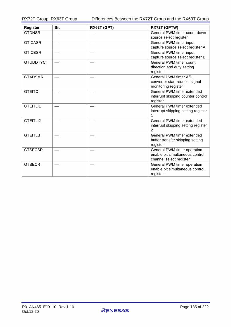
RX72T Group, RX63T Group Differences Between the RX72T Group and the RX63T Group
R01AN4651EJ0110 Rev.1.10 Page 135 of 222
Oct.12.20
Register Bit RX63T (GPT) RX72T (GPTW)
GTDNSR ⎯ ⎯ General PWM timer count-down
source select register
GTICASR ⎯ ⎯ General PWM timer input
capture source select register A
GTICBSR ⎯ ⎯ General PWM timer input
capture source select register B
GTUDDTYC ⎯ ⎯ General PWM timer count
direction and duty setting
register
GTADSMR ⎯ ⎯ General PWM timer A/D
converter start request signal
monitoring register
GTEITC ⎯ ⎯ General PWM timer extended
interrupt skipping counter control
register
GTEITLI1 ⎯ ⎯ General PWM timer extended
interrupt skipping setting register
1
GTEITLI2 ⎯ ⎯ General PWM timer extended
interrupt skipping setting register
2
GTEITLB ⎯ ⎯ General PWM timer extended
buffer transfer skipping setting
register
GTSECSR ⎯ ⎯ General PWM timer operation
enable bit simultaneous control
channel select register
GTSECR ⎯ ⎯ General PWM timer operation
enable bit simultaneous control
register

RX72T Group, RX63T Group Differences Between the RX72T Group and the RX63T Group
R01AN4651EJ0110 Rev.1.10 Page 136 of 222
Oct.12.20
Table 2.65 Comparative Listing of GTIOA and GTIOB Bit Settings
Bit
RX63T (GPT) RX72T (GPTW)
GTIOA/GTIOB[5:0] Bits GTIOA/GTIOB[4:0] Bits
b5 0: Compare match
1: Input capture
⎯
b4 • When b5 = 0
0: Initial output is low-level
1: Initial output is high-level
• When b5 = 1
x: Don’t care
0: Initial output is low-level
1: Initial output is high-level
b3, b2 • When b5 = 0
0 0: Output retained at cycle end
0 1: Low-level output at cycle end
1 0: High-level output at cycle end
1 1: Toggle output at cycle end
• When b5 = 1
x: Don’t care
0 0: Output retained at cycle end
0 1: Low-level output at cycle end
1 0: High-level output at cycle end
1 1: Toggle output at cycle end
b1, b0 • When b5 = 0
0 0: Output retained at GPTn.GTCCRA/GPTn.GTCCRB compare match
0 1: Low-level output at GPTn.GTCCRA/GPTn.GTCCRB compare match
1 0: High-level output at GPTn.GTCCRA/GPTn.GTCCRB compare match
1 1: Toggle output at GPTn.GTCCRA/GPTn.GTCCRB compare match
• When b5 = 1
0 0: Input capture at rising edge
0 1: Input capture at falling edge
1 0: Input capture at both edges
1 1: Input capture at both edges
0 0: Output retained at GTCCRA/GTCCRB register compare match
0 1: Low-level output at GTCCRA/GTCCRB register compare match
1 0: High-level output at GTCCRA/GTCCRB register compare match
1 1: Toggle output at GTCCRA/GTCCRB register compare match

RX72T Group, RX63T Group Differences Between the RX72T Group and the RX63T Group
R01AN4651EJ0110 Rev.1.10 Page 137 of 222
Oct.12.20
2.21 Compare Match Timer
Table 2.66 is a comparative overview of general compare match timer
Table 2.66 Comparative Overview of Compare Match Timer
Item RX63T (CMT) RX72T (CMT)
Count clocks Four frequency-divided clocks:
One clock among PCLK/8, PCLK/32,
PCLK/128, and PCLK/512 can be
selected independently for each
channel.
Four frequency-divided clocks:
One clock among PCLK/8, PCLK/32,
PCLK/128, and PCLK/512 can be
selected for each channel.
Interrupts A compare match interrupt can be
requested independently for each
channel.
A compare match interrupt can be
requested for each channel.
Event link function
(output)
⎯ An event signal is output at CMT1
compare match.
Event link function
(input)
⎯ • Ability to link to a specified module
• Support for CMT1 count start,
event counter, or count restart
operation
Low power consumption
function
Each unit can be placed in the
module-stop state.
Each unit can be placed in the
module-stop state.

RX72T Group, RX63T Group Differences Between the RX72T Group and the RX63T Group
R01AN4651EJ0110 Rev.1.10 Page 138 of 222
Oct.12.20
2.22 Watchdog Timer
Table 2.67 is a comparative overview of the watchdog timers, and Table 2.68 is a comparison of watchdog timer registers.
Table 2.67 Comparative Overview of Watchdog Timers
Item RX63T (WDTA) RX72T (WDTA)
Count source Peripheral clock (PCLK) Peripheral module clock (PCLK)
Clock division ratio Division by 4, 64, 128, 512, 2,048, or
8,192
Division by 4, 64, 128, 512, 2,048, or
8,192
Counter operation Counting down using a 14-bit down-
counter
Counting down using a 14-bit down-
counter
Conditions for
starting the counter • Counting starts automatically after a
reset, underflow, or generation of a
refresh error (auto-start mode).
• Counting is started by a refresh
(writing 00h and then FFh to the
WDTRR register) (register start
mode).
• Auto-start mode: Counting starts
automatically after a reset is
canceled.
• Register start mode: Counting is
started by refresh operation (writing
00h and then FFh to the WDTRR
register).
Conditions for
stopping the counter • A reset occurs. (The down-counter
and registers return to their initial
values.)
• A counter underflows or a refresh
error is generated (auto-start mode:
automatic, register start mode: by a
refresh).
• A reset occurs. (The down-counter
and registers return to their initial
values.)
• In a low power consumption state
• A counter underflows or a refresh
error occurs (register start mode
only)
Window function Window start and end positions can be
specified (for periods when refreshed
are permitted or prohibited).
Window start and end positions can be
specified (for periods when refreshed
are permitted or prohibited).
Reset output sources • Down-counter underflow
• Refresh outside the refresh-
permitted period (refresh error)
• Down-counter underflow
• Refresh outside the refresh-
permitted period (refresh error)
Interrupt request
output sources • When a non-maskable interrupt
(WUNI) is generated by an
underflow of the down-counter
• When a refresh occurs outside the
refresh-permitted period (refresh
error)
• When a non-maskable interrupt or
interrupt (WUNI) is generated by an
underflow of the down-counter
• When a refresh occurs outside the
refresh-permitted period (refresh
error)
Reading the counter
value
The down-counter value can be read
from the WDTSR register.
The down-counter value can be read
from the WDTSR register.
Output signals
(internal signals) • Reset output
• Non-maskable interrupt request
output
• Reset output
• Non-maskable interrupt request
output
• Interrupt request output

RX72T Group, RX63T Group Differences Between the RX72T Group and the RX63T Group
R01AN4651EJ0110 Rev.1.10 Page 139 of 222
Oct.12.20
Item RX63T (WDTA) RX72T (WDTA)
Auto-start mode
(controlled by option
function select
register 0 (OFS0))
• Selection of clock frequency division
ratio after a reset
(OFS0.WDTCKS[3:0] bits)
• Selection of time-out period of
watchdog timer
(OFS0.WDTTOPS[1:0] bits)
• Selection of window start position in
the watchdog timer
(OFS0.WDTRPSS[1:0] bits)
• Selection of window end position in
the watchdog timer
(OFS0.WDTRPES[1:0] bits)
• Selection of reset output or interrupt
request output
(OFS0.WDTRSTIRQS bit)
• Selection of clock frequency division
ratio after a reset
(OFS0.WDTCKS[3:0] bits)
• Selection of timeout period of
watchdog timer
(OFS0.WDTTOPS[1:0] bits)
• Selection of window start position in
the watchdog timer
(OFS0.WDTRPSS[1:0] bits)
• Selection of window end position in
the watchdog timer
(OFS0.WDTRPES[1:0] bits)
• Selection of reset output or interrupt
request output
(OFS0.WDTRSTIRQS bit)
Register start mode
(controlled by WDT
registers)
• Selection of clock frequency division
ratio after a refresh
(WDTCR.CKS[3:0] bits)
• Selection of time-out period of
watchdog timer (WDTCR.TOPS[1:0]
bits)
• Selection of window start position in
the watchdog timer
(WDTCR.RPSS[1:0] bits)
• Selection of window end position in
the watchdog timer
(WDTCR.RPES[1:0] bits)
• Selection of reset output or interrupt
request output (WDTRCR.RSTIRQS
bit)
• Selection of clock frequency division
ratio after a refresh
(WDTCR.CKS[3:0] bits)
• Selection of timeout period of
watchdog timer (WDTCR.TOPS[1:0]
bits)
• Selection of window start position in
the watchdog timer
(WDTCR.RPSS[1:0] bits)
• Selection of window end position in
the watchdog timer
(WDTCR.RPES[1:0] bits)
• Selection of reset output or interrupt
request output (WDTRCR.RSTIRQS
bit)
Table 2.68 Comparison of Watchdog Timer Registers
Register Bit RX63T (WDTA) RX72T (WDTA)
WDTRCR RSTIRQS Reset interrupt request selection
bit
0: Non-maskable interrupt request
output is enabled.
1: Reset output is enabled.
Reset interrupt request selection
bit
0: Non-maskable interrupt request
or interrupt request output is
enabled.*1
1: Reset output is enabled.
Note: 1. When the value of the NMIER.WDTEN bit is 1 non-maskable interrupts, and when it is 0 maskable
interrupts, are generated.

RX72T Group, RX63T Group Differences Between the RX72T Group and the RX63T Group
R01AN4651EJ0110 Rev.1.10 Page 140 of 222
Oct.12.20
2.23 Independent Watchdog Timer
Table 2.69 is a comparative overview of the independent watchdog timers, and Table 2.70 is a comparison of independent watchdog timer registers.
Table 2.69 Comparative Overview of Independent Watchdog Timers
Item RX63T (IWDTa) RX72T (IWDTa)
Count source IWDT-dedicated clock (IWDTCLK) IWDT-dedicated clock (IWDTCLK)
Clock division ratio Division by 1, 16, 32, 64, 128, or 256 Division by 1, 16, 32, 64, 128, or 256
Counter operation Counting down using a 14-bit down-
counter
Counting down using a 14-bit down-
counter
Conditions for
starting the counter • Counting starts automatically after a
reset (auto-start mode).
• Counting is started by a refresh
(writing 00h and then FFh to the
IWDTRR register) (register start
mode).
• Auto-start mode: Counting starts
automatically after a reset is
canceled.
• Register start mode: Counting is
started by refresh operation (writing
00h and then FFh to the IWDTRR
register).
Conditions for
stopping the counter • A reset occurs. (The down-counter
and registers return to their initial
values.)
• In a low power consumption state
(depending on register setting)
• A counter underflows or a refresh
error is generated (auto-start mode:
automatic, register start mode: by a
refresh).
• A reset occurs. (The down-counter
and registers return to their initial
values.)
• In a low power consumption state
(depending on register setting)
• A counter underflows or a refresh
error occurs (register start mode
only)
Window function Window start and end positions can be
specified (for periods when refreshed
are permitted or prohibited).
Window start and end positions can be
specified (for periods when refreshed
are permitted or prohibited).
Reset output sources • Down-counter underflow
• Refresh outside the refresh-
permitted period (refresh error)
• Down-counter underflow
• Refresh outside the refresh-
permitted period (refresh error)
Non-maskable
interrupt/interrupt
sources
• When a non-maskable interrupt
(WUNI) is generated by an
underflow of the down-counter
• When a refresh occurs outside the
refresh-permitted period (refresh
error)
• When a non-maskable interrupt or
interrupt (WUNI) is generated by an
underflow of the down-counter
• When a refresh occurs outside the
refresh-permitted period (refresh
error)
Reading the counter
value
The down-counter value can be read
from the IWDTSR register.
The down-counter value can be read
from the IWDTSR register.
Output signals
(internal signals) • Reset output
• Interrupt request output
• Sleep mode count stop control
output
• Reset output
• Interrupt request output
• Sleep mode count stop control
output
Event link function
(output)
⎯ • Down-counter underflow event
output
• Refresh error event output

RX72T Group, RX63T Group Differences Between the RX72T Group and the RX63T Group
R01AN4651EJ0110 Rev.1.10 Page 141 of 222
Oct.12.20
Item RX63T (IWDTa) RX72T (IWDTa)
Auto-start mode
(controlled by option
function select
register 0 (OFS0))
• Selection of clock frequency division
ratio after a reset
(OFS0.IWDTCKS[3:0] bits)
• Selection of time-out period of
watchdog timer
(OFS0.IWDTTOPS[1:0] bits)
• Selection of window start position in
the watchdog timer
(OFS0.IWDTRPSS[1:0] bits)
• Selection of window end position in
the watchdog timer
(OFS0.IWDTRPES[1:0] bits)
• Selection of reset output or interrupt
request output
(OFS0.IWDTRSTIRQS bit)
• Selection of down-count stop
function at transition to sleep mode,
software standby mode, deep
software standby mode, or all-
module clock stop mode
(OFS0.IWDTSLCSTP bit)
• Selection of clock frequency division
ratio after a reset
(OFS0.IWDTCKS[3:0] bits)
• Selection of timeout period of
independent watchdog timer
(OFS0.IWDTTOPS[1:0] bits)
• Selection of window start position in
the independent watchdog timer
(OFS0.IWDTRPSS[1:0] bits)
• Selection of window end position in
the independent watchdog timer
(OFS0.IWDTRPES[1:0] bits)
• Selection of reset output or interrupt
request output
(OFS0.IWDTRSTIRQS bit)
• Selection of down-count stop
function at transition to sleep mode,
software standby mode, deep
software standby mode, or all-
module clock stop mode
(OFS0.IWDTSLCSTP bit)
Register start mode
(controlled by IWDT
registers)
• Selection of clock frequency division
ratio after a refresh
(IWDTCR.CKS[3:0] bits)
• Selection of time-out period of
watchdog timer (IWDTCR.TOPS[1:0]
bits)
• Selection of window start position in
the watchdog timer
(IWDTCR.RPSS[1:0] bits)
• Selection of window end position in
the watchdog timer
(IWDTCR.RPES[1:0] bits)
• Selection of reset output or interrupt
request output
(IWDTRCR.RSTIRQS bit)
• Selection of down-count stop
function at transition to sleep mode,
software standby mode, deep
software standby mode, or all-
module clock stop mode
(IWDTCSTPR.SLCSTP bit)
• Selection of clock frequency division
ratio after a refresh
(IWDTCR.CKS[3:0] bits)
• Selection of timeout period of
independent watchdog timer
(IWDTCR.TOPS[1:0] bits)
• Selection of window start position in
the independent watchdog timer
(IWDTCR.RPSS[1:0] bits)
• Selection of window end position in
the independent watchdog timer
(IWDTCR.RPES[1:0] bits)
• Selection of reset output or interrupt
request output
(IWDTRCR.RSTIRQS bit)
• Selection of down-count stop
function at transition to sleep mode,
software standby mode, deep
software standby mode, or all-
module clock stop mode
(IWDTCSTPR.SLCSTP bit)
Table 2.70 Comparison of Independent Watchdog Timer Registers
Register Bit RX63T (IWDTa) RX72T (IWDTa)
IWDTRCR RSTIRQS Reset interrupt request selection
bit
0: Non-maskable interrupt request
output is enabled.
1: Reset output is enabled.
Reset interrupt request selection
bit
0: Non-maskable interrupt request
or interrupt request output is
enabled.*1
1: Reset output is enabled.
Note: 1. When the value of the NMIER.IWDTEN bit is 1 non-maskable interrupts, and when it is 0 maskable
interrupts, are generated.

RX72T Group, RX63T Group Differences Between the RX72T Group and the RX63T Group
R01AN4651EJ0110 Rev.1.10 Page 142 of 222
Oct.12.20
2.24 USB 2.0 FS Host/Function Module
Table 2.71 is a comparative overview of USB 2.0 FS Host/Function module, and Table 2.72 is a comparison of USB 2.0 FS Host/Function module registers.
Table 2.71 Comparative Overview of USB 2.0 FS Host/Function Module
Item RX63T (USBa) RX72T (USBb)
Features • Built-in USB device controller (UDC)
and transceiver for USB 2.0
⎯ One port is provided.
⎯ USB0: Support for Host
controller, Function controller,
and OTG
• Built-in Host controller and Function
controller (switchable by software)
• Selectable between self-power mode
and bus-power mode
• Support for OTG (On-The-Go)
• Built-in USB device controller (UDC)
and transceiver for USB 2.0
⎯ Support for Host controller,
Function controller, and On-The-
Go (OTG) (one channel)
• Ability to switch between Host
controller and Function controller by
software
• Selectable between self-power mode
and bus-power mode
• Support for OTG (On-The-Go)
When the Host controller function is
selected
• Full-speed transfer (12 Mbps) is
supported.
• Multiple peripheral devices can be
connected for communication via a
one-stage hub.
• Scheduling of SOF and packet
transmission is automated.
• Transfer intervals can be specified
for isochronous and interrupt
transfers.
When the Host controller function is
selected
• Full-speed transfer (12 Mbps) and
low-speed transfer (1.5 Mbps) are
supported.
• Multiple peripheral devices can be
connected for communication via a
one-stage hub.
• Scheduling of SOF and packet
transmission is automated.
• Transfer intervals can be specified
for isochronous and interrupt
transfers.
When the Function controller function is
selected
• Full-speed transfer (12 Mbps) is
supported.*1
• Control transfer stage control
function
• Device state control function
• Auto response function for
SET_ADDRESS requests
• SOF recovery function
When the Function controller function is
selected
• Full-speed transfer (12 Mbps) is
supported.*1
• Control transfer stage control
function
• Device state control function
• Auto response function for
SET_ADDRESS requests
• SOF recovery function
Communication data
transfer types • Control transfer
• Bulk transfer
• Interrupt transfer
• Isochronous transfer
• Control transfer
• Bulk transfer
• Interrupt transfer
• Isochronous transfer
Internal bus interface Connected to internal peripheral bus 3 Connected to internal peripheral bus 3

RX72T Group, RX63T Group Differences Between the RX72T Group and the RX63T Group
R01AN4651EJ0110 Rev.1.10 Page 143 of 222
Oct.12.20
Item RX63T (USBa) RX72T (USBb)
Pipe configuration • Buffer memory for USB
communication is provided.
• Up to ten pipes can be selected
(including the default control pipe).
• Endpoint numbers can be assigned
flexibly to PIPE1 to PIPE9.
• Buffer memory for USB
communication is provided.
• Up to ten pipes can be selected
(including the default control pipe).
• Endpoint numbers can be assigned
flexibly to PIPE1 to PIPE9.
Transfer conditions that can be set for
each pipe
• PIPE0:
Control transfer only (default control
pipe: DPC), buffer size of 8, 16, 32,
or 64 bytes (single buffer)
Transfer conditions that can be set for
each pipe
• PIPE0:
Control transfer, 64-byte single
buffer
• PIPE1 and PIPE2:
Bulk transfer or isochronous transfer,
buffer size of 8, 16, 32, or 64 bytes
for bulk transfer or 1 to 256 bytes for
isochronous transfer (double buffer
support)
• PIPE3 to PIPE5:
Bulk transfer only, buffer size of 8,
16, 32, or 64 bytes (double buffer
support)
• PIPE6 to PIPE9:
Interrupt transfer only, buffer size of
1 to 64 bytes (single buffer)
• PIPE1 and PIPE2:
64-byte double buffer can be
specified for bulk transfer and 256-
byte double buffer for isochronous
transfer.
• PIPE3 to PIPE5:
64-byte double buffer can be
specified for bulk transfer.
• PIPE6 to PIPE9:
64-byte single buffer can be
specified for interrupt transfer.
Other functions • Reception transfer end function
using transaction count
• Function for changing BRDY
interrupt event notification timing
(BFRE)
• Function that automatically clears
the buffer memory after the data for
the pipe specified at DnFIFO (n = 0
or 1) port has been read (DCLRM)
• NAK setting function for response
PID generated at transfer end
(SHTNAK)
• Reception transfer end function
using transaction count
• Function for changing BRDY
interrupt event notification timing
(BFRE)
• Function that automatically clears
the buffer memory after the data for
the pipe specified at DnFIFO (n = 0
or 1) has been read (DCLRM)
• NAK setting function for response
PID generated at transfer end
(SHTNAK)
• On-chip D+/D− pull-up and pull-
down resistors
Low power
consumption function
Ability to specify transition to module
stop state
Ability to transition to module stop state
Note: 1. Low-speed transfer (1.5 Mbps) is not supported.

RX72T Group, RX63T Group Differences Between the RX72T Group and the RX63T Group
R01AN4651EJ0110 Rev.1.10 Page 144 of 222
Oct.12.20
Table 2.72 Comparison of USB 2.0 FS Host/Function Module Registers
Register Bit RX63T (USBa) RX72T (USBb)
DVSTCTR0 RHST[2:0] USB bus reset status bits
When the Host controller function
is selected
b2 b0
0 0 0: Communication speed
undetermined (powered
state or no connection)
1 x x: USB bus reset in progress
0 0 1: Low-speed connection*1
0 1 0: Full-speed connection
When the Function controller
function is selected
b2 b0
0 0 0: Communication speed
undetermined
0 1 0: USB bus reset in progress
or full-speed connection
USB bus reset status flag
When the Host controller function
is selected
b2 b0
0 0 0: Communication speed
undetermined (powered
state or no connection)
1 x x: USB bus reset in progress
0 0 1: Low-speed connection
0 1 0: Full-speed connection
When the Function controller
function is selected
b2 b0
0 0 0: Communication speed
undetermined
0 0 1: USB bus reset in progress
0 1 0: USB bus reset in progress
or full-speed connection
SOFCFG TRNENSEL ⎯ Transaction-enabled time select
bit
PHYSLEW ⎯ ⎯ PHY cross point adjustment
register
DVCHGR ⎯ Device state change register ⎯
USBADDR ⎯ USB address register ⎯
DEVADDn
(n = 0 to 5)
USBSPD[1:0] Transfer speed of communication
target device bits
b7 b6
0 0: DEVADDn register not used
0 1: Setting prohibited.
1 0: Full speed
1 1: Setting prohibited.
Transfer speed of communication
target device bits
b7 b6
0 0: DEVADDn register not used
0 1: Low speed
1 0: Full speed
1 1: Setting prohibited.
Note: 1. The USB controller does not support communication with low-speed devices. If this value is read,
abnormal connection processing should be performed by a higher application.
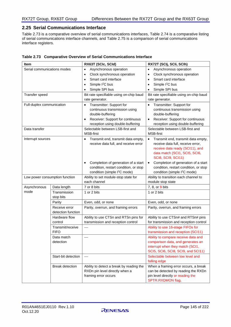
RX72T Group, RX63T Group Differences Between the RX72T Group and the RX63T Group
R01AN4651EJ0110 Rev.1.10 Page 145 of 222
Oct.12.20
2.25 Serial Communications Interface
Table 2.73 is a comparative overview of serial communications interfaces, Table 2.74 is a comparative listing of serial communications interface channels, and Table 2.75 is a comparison of serial communications interface registers.
Table 2.73 Comparative Overview of Serial Communications Interface
Item RX63T (SCIc, SCId) RX72T (SCIj, SCIi, SCIh)
Serial communications modes • Asynchronous operation
• Clock synchronous operation
• Smart card interface
• Simple I2C bus
• Simple SPI bus
• Asynchronous operation
• Clock synchronous operation
• Smart card interface
• Simple I2C bus
• Simple SPI bus
Transfer speed Bit rate specifiable using on-chip baud
rate generator.
Bit rate specifiable using on-chip baud
rate generator.
Full-duplex communication • Transmitter: Support for
continuous transmission using
double-buffering
• Receiver: Support for continuous
reception using double-buffering
• Transmitter: Support for
continuous transmission using
double-buffering
• Receiver: Support for continuous
reception using double-buffering
Data transfer Selectable between LSB-first and
MSB-first
Selectable between LSB-first and
MSB-first
Interrupt sources • Transmit end, transmit data empty,
receive data full, and receive error
• Completion of generation of a start
condition, restart condition, or stop
condition (simple I2C mode)
• Transmit end, transmit data empty,
receive data full, receive error,
receive data ready (SCI11), and
data match (SCI1, SCI5, SCI6,
SCI8, SCI9, SCI11)
• Completion of generation of a start
condition, restart condition, or stop
condition (simple I2C mode)
Low power consumption function Ability to set module-stop state for
each channel
Ability to transition each channel to
module stop state
Asynchronous
mode
Data length 7 or 8 bits 7, 8, or 9 bits
Transmission
stop bits
1 or 2 bits 1 or 2 bits
Parity Even, odd, or none Even, odd, or none
Receive error
detection function
Parity, overrun, and framing errors Parity, overrun, and framing errors
Hardware flow
control
Ability to use CTSn and RTSn pins for
transmission and reception control
Ability to use CTSn# and RTSn# pins
for transmission and reception control
Transmit/receive
FIFO
⎯ Ability to use 16-stage FIFOs for
transmission and reception (SCI11)
Data match
detection
⎯ Ability to compare receive data and
comparison data, and generates an
interrupt when they match (SCI1,
SCI5, SCI6, SCI8, SCI9, and SCI11)
Start-bit detection ⎯ Selectable between low level and
falling edge
Break detection Ability to detect a break by reading the
RXDn pin level directly when a
framing error occurs
When a framing error occurs, a break
can be detected by reading the RXDn
pin level directly or reading the
SPTR.RXDMON flag.

RX72T Group, RX63T Group Differences Between the RX72T Group and the RX63T Group
R01AN4651EJ0110 Rev.1.10 Page 146 of 222
Oct.12.20
Item RX63T (SCIc, SCId) RX72T (SCIj, SCIi, SCIh)
Asynchronous
mode
Clock source • Selectable between internal or
external clock
• Ability to input transfer rate clock
from MTU3
• Selectable between internal or
external clock
• Ability to input transfer rate clock
from TMR (SCI5, SCI6, and
SCI12)
Double-speed
mode
⎯ Ability to select baud rate generator
double-speed mode
Multi-processor
communications
function
Serial communication among multiple
processors
Serial communication among multiple
processors
Noise
cancellation
function
The input signal paths from the RXDn
pins incorporate digital noise filters.
The input signal paths from the RXDn
pins incorporate digital noise filters.
Clock
synchronous
mode
Data length 8 bits 8 bits
Receive error
detection
Overrun error Overrun error
Hardware flow
control
Ability to use CTSn and RTSn pins for
transmission and reception control
Ability to use CTSn# and RTSn# pins
for transmission and reception control
Transmit/receive
FIFO
⎯ Ability to use 16-stage FIFOs for
transmission and reception (SCI11)
Smart card
interface mode
Error processing • Automatic transmission of an error
signal at detection of a parity error
during reception
• Automatic re-transmission of data
at reception of an error signal
during transmission
• Automatic transmission of an error
signal at detection of a parity error
during reception
• Automatic re-transmission of data
at reception of an error signal
during transmission
Data type Support for direct convention and
inverse convention
Support for direct convention and
inverse convention
Simple I2C
mode
Communication
format
I2C bus format I2C bus format
Operating mode Master (single-master operation only) Master (single-master operation only)
Transfer speed • Support for fast mode (Refer to
description of bit rate register
(BRR) for details on setting the
transfer rate.) (SCI0 to SCI3)
• Max. 384 kbps (SCI12)
• Support for fast mode (Refer to
description of bit rate register
(BRR) for details on setting the
transfer rate.)
Noise
cancellation
• The SSCLn and SSDAn input
signal paths incorporate digital
noise filters.
• The noise cancellation interval is
adjustable.
• The SSCLn and SSDAn input
signal paths incorporate digital
noise filters.
• The noise cancellation interval is
adjustable.
Simple SPI
mode
Data length 8 bits 8 bits
Error detection Overrun error Overrun error
SS input pin
function
Ability to place output pins in high-
impedance state by applying a high-
level signal to the SSn# pin.
Ability to place output pins in high-
impedance state by applying a high-
level signal to the SSn# pin.
Clock settings Ability to select among four clock
phase and clock polarity settings
Ability to select among four clock
phase and clock polarity settings
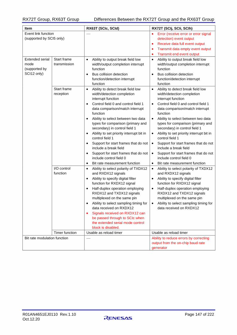
RX72T Group, RX63T Group Differences Between the RX72T Group and the RX63T Group
R01AN4651EJ0110 Rev.1.10 Page 147 of 222
Oct.12.20
Item RX63T (SCIc, SCId) RX72T (SCIj, SCIi, SCIh)
Event link function
(supported by SCI5 only)
⎯ • Error (receive error or error signal
detection) event output
• Receive data full event output
• Transmit data empty event output
• Transmit end event output
Extended serial
mode
(supported by
SCI12 only)
Start frame
transmission
• Ability to output break field low
width/output completion interrupt
function
• Bus collision detection
function/detection interrupt
function
• Ability to output break field low
width/output completion interrupt
function
• Bus collision detection
function/detection interrupt
function
Start frame
reception
• Ability to detect break field low
width/detection completion
interrupt function
• Control field 0 and control field 1
data comparison/match interrupt
function
• Ability to select between two data
types for comparison (primary and
secondary) in control field 1
• Ability to set priority interrupt bit in
control field 1
• Support for start frames that do not
include a break field
• Support for start frames that do not
include control field 0
• Bit rate measurement function
I/O control
function
• Ability to select polarity of TXDX12
and RXDX12 signals
• Ability to specify digital filter
function for RXDX12 signal
• Half-duplex operation employing
RXDX12 and TXDX12 signals
multiplexed on the same pin
• Ability to select sampling timing for
data received on RXDX12
• Signals received on RXDX12 can
be passed through to SCIc when
the extended serial mode control
block is disabled.
• Ability to select polarity of TXDX12
and RXDX12 signals
• Ability to specify digital filter
function for RXDX12 signal
• Half-duplex operation employing
RXDX12 and TXDX12 signals
multiplexed on the same pin
• Ability to select sampling timing for
data received on RXDX12
Timer function Usable as reload timer Usable as reload timer
Bit rate modulation function ⎯ Ability to reduce errors by correcting
output from the on-chip baud rate
generator

RX72T Group, RX63T Group Differences Between the RX72T Group and the RX63T Group
R01AN4651EJ0110 Rev.1.10 Page 148 of 222
Oct.12.20
Table 2.74 Comparative Listing of Serial Communications Interface Channels
Item RX63T (SCIc, SCId) RX72T (SCIj, SCIi, SCIh)
Asynchronous mode SCI0, SCI1, SCI2, SCI3, SCI12 SCI1, SCI5, SCI6, SCI8, SCI9,
SCI11, SCI12
Clock synchronous mode SCI0, SCI1, SCI2, SCI3, SCI12 SCI1, SCI5, SCI6, SCI8, SCI9,
SCI11, SCI12
Smart card interface mode SCI0, SCI1, SCI2, SCI3, SCI12 SCI1, SCI5, SCI6, SCI8, SCI9,
SCI11, SCI12
Simple I2C mode SCI0, SCI1, SCI2, SCI3, SCI12 SCI1, SCI5, SCI6, SCI8, SCI9,
SCI11, SCI12
Simple SPI mode SCI0, SCI1, SCI2, SCI3, SCI12 SCI1, SCI5, SCI6, SCI8, SCI9,
SCI11, SCI12
FIFO mode ⎯ SCI11
Data match detection ⎯ SCI1, SCI5, SCI6, SCI8, SCI9,
SCI11
Extended serial mode SCI12 SCI12
MTU3 clock input SCI0, SCI1, SCI2, SCI3, SCI12
(Not supported on 64- and 48-pin
products.)
⎯
TMR clock input ⎯ SCI5, SCI6, SCI12
Event link function ⎯ SCI5
Peripheral module clock PCLK PCLKB: SCI1, SCI5, SCI6, SCI8,
SCI9, SCI12
PCLKA: SCI11

RX72T Group, RX63T Group Differences Between the RX72T Group and the RX63T Group
R01AN4651EJ0110 Rev.1.10 Page 149 of 222
Oct.12.20
Table 2.75 Comparison of Serial Communications Interface Registers
Register Bit RX63T (SCIc, SCId) RX72T (SCIj,SCIi,SCIh)
RDRH ⎯ ⎯ Receive data register H
RDRL ⎯ ⎯ Receive data register L
RDRHL ⎯ ⎯ Receive data register HL
FRDR ⎯ ⎯ Receive FIFO data register
TDRH ⎯ ⎯ Transmit data register H
TDRL ⎯ ⎯ Transmit data register L
TDRHL ⎯ ⎯ Transmit data register HL
FTDR ⎯ Transmit FIFO data register
SCR
(When
SCMR.SMIF = 0)
CKE[1:0] Clock enable bits
(Asynchronous mode)
b1 b0
0 0: On-chip baud rate generator
By means of I/O port settings,
the SCKn pin can function as
an I/O port.
0 1: On-chip baud rate generator
Outputs a clock with the same
frequency as the bit rate
output from the SCKn pin.
1 x: External clock or MTU3 clock
• When an external clock is
used, a clock with a
frequency 16 times the bit
rate should be input on the
SCKn pin. Input a clock
signal with a frequency
eight times the bit rate
when the SEMR.ABCS bit
is set to 1.
• An MTU3 clock can be
used.
The base clock input on
MTU3 must be set to a
frequency no greater than
1/4 PCLK. When an MTU3
clock is used, the SCKn
pin can function as an I/O
port by means of I/O port
settings.
Clock enable bits
(Asynchronous mode)
b1 b0
0 0: On-chip baud rate generator
SCKn pin enters high-
impedance state.
0 1: On-chip baud rate generator
Outputs a clock with the same
frequency as the bit rate
output from the SCKn pin.
1 x: External clock or TMR clock
• When an external clock is
used, a clock with a
frequency 16 times the bit
rate should be input on the
SCKn pin. Input a clock
signal with a frequency
eight times the bit rate
when the SEMR.ABCS bit
is set to 1.
• When using the TMR
clock, the SCKn pin enters
the high-impedance state.
The TMR clock is
selectable for SCI5, SCI6,
and SCI12.
(Clock synchronous mode)
b1 b0
0 x: Internal clock
The SCKn pin functions as
the clock output pin.
1 x: External clock
The SCKn pin functions as
the clock input pin.
(Clock synchronous mode)
b1 b0
0 x: Internal clock
The SCKn pin functions as
the clock output pin.
1 x: External clock
The SCKn pin functions as
the clock input pin.

RX72T Group, RX63T Group Differences Between the RX72T Group and the RX63T Group
R01AN4651EJ0110 Rev.1.10 Page 150 of 222
Oct.12.20
Register Bit RX63T (SCIc, SCId) RX72T (SCIj,SCIi,SCIh)
SMR
(When
SCMR.SMIF = 0)
CHR Character length bit
(Valid in asynchronous mode
only.)
0: Transmit/receive using 8-bit
data length.
1: Transmit/receive using 7-bit
data length.
Character length bit
(Valid in asynchronous mode
only.)
Selection made in combination
with SCMR.CHR1 bit.
CHR1 CHR
0 0: Transmit/receive using 9-bit
data length.
0 1: Transmit/receive using 9-bit
data length.
1 0: Transmit/receive using 8-bit
data length. (initial value)
1 1: Transmit/receive using 7-bit
data length.
SSR
(When
SCMR.SMIF = 1)
RDRF ⎯ Receive data full flag
TDRE ⎯ Transmit data empty flag
SSR
(When
SCMR.SMIF = 0
and FCR.FM = 1)
DR ⎯ Receive data ready flag
TEND ⎯ Transmit end flag
PER ⎯ Parity error flag
FER ⎯ Framing error flag
ORER ⎯ Overrun error flag
RDF ⎯ Receive FIFO full flag
TDFE ⎯ Transmit FIFO empty flag
SSRFIFO ⎯ ⎯ Serial status register
SCMR CHR1 ⎯ Character length bit 1
MDDR ⎯ ⎯ Modulation duty register
SEMR ACS0 Asynchronous mode clock source
select bit
[144-, 120-, 112-, and 100-pin
versions]
(Valid in asynchronous mode
only.)
0: External clock input
1: MTU3 clock input
(MTIOC6A or MTIOC7A)
[64- and 48-pin versions]
This bit is read as 0. The write
value should be 0.
Asynchronous mode clock source
select bit
(Valid in asynchronous mode
only.)
0: External clock
1: Logical AND of two compare
matches output from TMR (valid
for SCI5, SCI6, and SCI12 only)
The available compare match
output varies among SCI
channels.
BRME ⎯ Bit rate modulation enable bit
ABCSE ⎯ Asynchronous mode base clock
select extended bit
BGDM ⎯ Baud rate generator double-speed
mode select bit
RXDESEL ⎯ Asynchronous start bit edge
detection select bit
FCR ⎯ ⎯ FIFO control register
FDR ⎯ ⎯ FIFO data count register

RX72T Group, RX63T Group Differences Between the RX72T Group and the RX63T Group
R01AN4651EJ0110 Rev.1.10 Page 151 of 222
Oct.12.20
Register Bit RX63T (SCIc, SCId) RX72T (SCIj,SCIi,SCIh)
LSR ⎯ ⎯ Line status register
CDR ⎯ ⎯ Comparison data register
DCCR ⎯ ⎯ Data comparison control register
SPTR ⎯ ⎯ Serial port register
CR2 BCCS[1:0] Bus collision detection clock select
bits
Bus collision detection clock select
bits
• When SEMR.BGDM = 0 or
SEMR.BGDM = 1 and
SMR.CKS[1:0] = a value other
than 00b
b5 b4
0 0: SCI Base clock frequency
0 1: SCI Base clock frequency
divided by 2
1 0: SCI Base clock frequency
divided by 4
1 1: Setting prohibited.
b5 b4
0 0: Base clock frequency
0 1: Base clock frequency divided
by 2
1 0: Base clock frequency divided
by 4
1 1: Setting prohibited.
• When SEMR.BGDM = 1 and
SMR.CKS[1:0] = 00b
b5 b4
0 0: Base clock frequency divided
by 2
0 1: Base clock frequency divided
by 4
1 0: Setting prohibited.
1 1: Setting prohibited.

RX72T Group, RX63T Group Differences Between the RX72T Group and the RX63T Group
R01AN4651EJ0110 Rev.1.10 Page 152 of 222
Oct.12.20
2.26 I2C Bus Interface
Table 2.76 is a comparative overview of I2C bus interface, and Table 2.77 is a comparison of I2C bus interface registers.
Table 2.76 Comparative Overview of I2C Bus Interface
Item RX63T (RIIC) RX72T (RIICa)
Number of channels 2 channels 1 channel
Communication
format • I2C bus format or SMBus format
• Selectable between master mode
and slave mode
• Automatic securing of set-up times,
hold times, and bus-free times to
match the specified transfer speed
• I2C bus format or SMBus format
• Selectable between master mode
and slave mode
• Automatic securing of set-up times,
hold times, and bus-free times to
match the specified transfer speed
Transfer speed Up to 400 kbps Support for fast mode (up to 400 kbps)
SCL clock Ability to select duty cycle of SCL clock
within range of 4% to 96% during
master operation
Ability to select duty cycle of SCL clock
within range of 4% to 96% during
master operation
Issuing and detecting
conditions • Automatic generation of start, restart,
and stop conditions
• Ability to detect start conditions
(including restart conditions) and
stop conditions
• Automatic generation of start, restart,
and stop conditions
• Ability to detect start conditions
(including restart conditions) and
stop conditions
Slave address • Ability to set up to three slave
addresses
• Support for 7- and 10-bit address
formats (along with use of both at
once)
• Ability to detect general call
addresses, device ID addresses, and
SMBus host addresses
• Ability to set up to three different
slave addresses
• Support for 7- and 10-bit address
formats (along with use of both at
once)
• Ability to detect general call
addresses, device ID addresses, and
SMBus host addresses
Acknowledgment • Automatic loading of acknowledge
bit during transmission
⎯ Ability to suspend the next data
transfer automatically on
detection of a not-acknowledge
bit
• Automatic transmission of
acknowledge bit during reception
⎯ Support for software control of
value of the acknowledge bit
according to the received data
when a wait between the eighth
and ninth clock cycles is selected
• Automatic loading of acknowledge
bit during transmission
⎯ Ability to suspend the next data
transfer automatically on
detection of a not-acknowledge
bit
• Automatic transmission of
acknowledge bit during reception
⎯ Support for software control of
value of the acknowledge bit
according to the received data
when a wait between the eighth
and ninth clock cycles is selected
Wait function • Ability to implement a wait by holding
the SCL clock signal low
• Wait between the eighth and ninth
clock cycles
• Wait between the ninth and first
clock cycles (WAIT function)
• Ability to implement a wait by holding
the SCL clock signal low
• Wait between the eighth and ninth
clock cycles
• Wait between the ninth and first
clock cycles
SDA output delay
function
Ability to delay output timing of
transmitted data, including the
acknowledge bit
Ability to delay output timing of
transmitted data, including the
acknowledge bit

RX72T Group, RX63T Group Differences Between the RX72T Group and the RX63T Group
R01AN4651EJ0110 Rev.1.10 Page 153 of 222
Oct.12.20
Item RX63T (RIIC) RX72T (RIICa)
Arbitration • Multi-master support
⎯ Ability to synchronize operation
with the clock of another master
in cases of conflict with the SCL
clock
⎯ Ability to detect loss of arbitration
in case of an SDA line signal
state mismatch when a start
condition issuance conflict occurs
⎯ Ability to detect loss of arbitration
when a start transmit data
mismatch occurs during master
operation
• Ability to detect loss of arbitration
due to start condition issuance when
the bus is busy (to prevent issuance
of duplicate start conditions)
• Ability to detect loss of arbitration in
case of an SDA line signal state
mismatch when a not-acknowledge
bit is sent
• Ability to detect loss of arbitration
when a data mismatch occurs during
slave transmission
• Multi-master support
⎯ Ability to synchronize operation
with the clock of another master
in cases of conflict with the SCL
clock
⎯ Ability to detect loss of arbitration
in case of an SDA line signal
state mismatch when a start
condition issuance conflict occurs
⎯ Ability to detect loss of arbitration
when a start transmit data
mismatch occurs during master
operation
• Ability to detect loss of arbitration
due to start condition issuance when
the bus is busy (to prevent issuance
of duplicate start conditions)
• Ability to detect loss of arbitration in
case of an SDA line signal state
mismatch when a not-acknowledge
bit is sent
• Ability to detect loss of arbitration
when a data mismatch occurs during
slave transmission
Timeout detection function
Ability to detect extended stopping of
the SCL clock using built-in time-out
function
Ability to detect extended stopping of
the SCL clock using built-in time-out
function
Noise cancellation Built-in digital noise filters for SCL and
SDA signals, and ability to adjust the
noise cancellation width by software.
Built-in digital noise filters for SCL and
SDA signals, and ability to adjust the
noise cancellation width by software.
Interrupt sources Four sources
• Communication error/event
occurrence (AL detection, NACK
detection, timeout detection, start
condition (including restart condition)
detection, or stop condition
detection)
• Receive data full (including match
with slave address)
• Transmit data empty (including
match with slave address)
• Transmission complete
Four sources
• Communication error/event
occurrence, arbitration detection,
NACK detection, timeout detection,
start condition (including restart
condition) detection, or stop
condition detection
• Receive data full (including match
with slave address)
• Transmit data empty (including
match with slave address)
• Transmission complete
Low power
consumption function
Ability to specify transition to module
stop state
Ability to transition to module stop state
RIIC operating
modes
Four modes:
Master transmit mode, master receive
mode, slave transmit mode, and slave
receive mode
Four modes:
Master transmit mode, master receive
mode, slave transmit mode, and slave
receive mode

RX72T Group, RX63T Group Differences Between the RX72T Group and the RX63T Group
R01AN4651EJ0110 Rev.1.10 Page 154 of 222
Oct.12.20
Item RX63T (RIIC) RX72T (RIICa)
Event link function
(output)
⎯ Four sources (RIIC0)
• Communication error/event
occurrence, arbitration detection,
NACK detection, timeout detection,
start condition (including restart
condition) detection, or stop
condition detection
• Receive data full (including match
with slave address)
• Transmit data empty (including
match with slave address)
• Transmission complete
Table 2.77 Comparison of I2C Bus Interface Registers
Register Bit RX63T (RIIC) RX72T (RIICa)
ICMR2 TMWE Timeout internal counter write
enable bit
⎯
TMOCNT ⎯ Timeout internal counter ⎯

RX72T Group, RX63T Group Differences Between the RX72T Group and the RX63T Group
R01AN4651EJ0110 Rev.1.10 Page 155 of 222
Oct.12.20
2.27 CAN Module
Table 2.78 is a comparative overview of CAN module.
Table 2.78 Comparative Overview of CAN Module
Item RX63T (CAN) RX72T (CAN)
Number of channels 3 channels 1 channel
Protocol ISO 11898-1 compliant (standard and
extended frames)
ISO 11898-1 compliant (standard and
extended frames)
Bit rate • Programmable bit rate up to 1 Mbps
(fCAN ≥ 8 MHz)
• fCAN: CAN clock source
• Programmable bit rate up to 1 Mbps
(fCAN ≥ 8 MHz)
• fCAN: CAN clock source
Message box • 32 mailboxes:
Two selectable mailbox modes
• Normal mailbox mode:
⎯ 32 mailboxes can be configured
for either transmission or
reception.
• FIFO mailbox mode:
⎯ 24 mailboxes can be configured
for either transmission or
reception.
⎯ The remaining mailboxes can be
configured as four FIFO
transmission stages and four
FIFO reception stages.
• 32 mailboxes:
Two selectable mailbox modes
• Normal mailbox mode:
⎯ 32 mailboxes can be configured
for either transmission or
reception.
• FIFO mailbox mode:
⎯ 24 mailboxes can be configured
for either transmission or
reception.
⎯ The remaining mailboxes can be
configured as four FIFO
transmission stages and four
FIFO reception stages.
Reception • Ability to receive data frames and
remote frames
• Selectable ID reception format (only
standard IDs, only extended IDs, or
both standard and extended IDs)
• Ability to select one-shot reception
function
• Ability to select among overwrite
mode (messages are overwritten)
and overrun mode (messages are
discarded)
• Ability to enable or disable reception
complete interrupt individually for
each mailbox
• Ability to receive data frames and
remote frames
• Selectable ID reception format (only
standard IDs, only extended IDs, or
both standard and extended IDs)
• Ability to select one-shot reception
function
• Ability to select among overwrite
mode (messages are overwritten)
and overrun mode (messages are
discarded)
• Ability to enable or disable reception
complete interrupt individually for
each mailbox
Acceptance filter • Eight acceptance masks (one mask
for every four mailboxes)
• Ability to enable or disable masks
individually for each mailbox
• Eight acceptance masks (one mask
for every four mailboxes)
• Ability to enable or disable masks
individually for each mailbox

RX72T Group, RX63T Group Differences Between the RX72T Group and the RX63T Group
R01AN4651EJ0110 Rev.1.10 Page 156 of 222
Oct.12.20
Item RX63T (CAN) RX72T (CAN)
Transmission • Ability to transmit data frames and
remote frames
• Ability to select ID transmission
format (only standard IDs, only
extended IDs, or both standard and
extended IDs)
• Ability to select one-shot
transmission function
• Ability to select between ID priority
mode and mailbox number priority
mode
• Ability to abort transmission requests
(and ability to confirm abort
completion with a flag)
• Ability to enable or disable
transmission complete interrupt
individually for each mailbox
• Ability to transmit data frames and
remote frames
• Ability to select ID transmission
format (only standard IDs, only
extended IDs, or both standard and
extended IDs)
• Ability to select one-shot
transmission function
• Ability to select between ID priority
mode and mailbox number priority
mode
• Ability to abort transmission requests
(and ability to confirm abort
completion with a flag)
• Ability to enable or disable
transmission complete interrupt
individually for each mailbox
Bus-off recovery
methods • Ability to select method of recovery
from the bus-off state
• ISO 11898-1 compliant
• Automatic transition to CAN halt
mode at bus-off start
• Automatic transition to CAN halt
mode at bus-off end
• Transition to CAN halt mode by
software
• Transition to error-active state by
software
• Ability to select method of recovery
from the bus-off state
• ISO 11898-1 compliant
• Automatic transition to CAN halt
mode at bus-off start
• Automatic transition to CAN halt
mode at bus-off end
• Transition to CAN halt mode by
software
• Transition to error-active state by
software
Error status
monitoring • Ability to monitor CAN bus errors
(stuffing error, form error, ACK error,
CRC error, bit error, and ACK
delimiter error)
• Ability to transitions to error states
(error-warning, error-passive, bus-off
start, and bus-off recovery)
• Ability to read error counters
• Ability to monitor CAN bus errors
(stuffing error, form error, ACK error,
CRC error, bit error, and ACK
delimiter error)
• Ability to transitions to error states
(error-warning, error-passive, bus-off
start, and bus-off recovery)
• Ability to read error counters
Time stamp function • Time stamp function using 16-bit
counter
• Ability to select reference clock
among 1-, 2-, 4- and 8-bit time
durations
• Time stamp function using 16-bit
counter
• Ability to select reference clock
among 1-, 2-, 4- and 8-bit time
durations
Interrupt function Five interrupt sources (reception
complete, transmission complete,
receive FIFO, transmit FIFO, and error
interrupts)
Five interrupt sources (reception
complete, transmission complete,
receive FIFO, transmit FIFO, and error
interrupts)
CAN sleep mode Ability to reduce current consumption by
stopping the CAN clock
Ability to reduce current consumption by
stopping the CAN clock
Software support
units
Three software support units
• Acceptance filter support
• Mailbox search support (receive
mailbox search, transmit mailbox
search, and message lost search)
• Channel search support
Three software support units
• Acceptance filter support
• Mailbox search support (receive
mailbox search, transmit mailbox
search, and message lost search)
• Channel search support

RX72T Group, RX63T Group Differences Between the RX72T Group and the RX63T Group
R01AN4651EJ0110 Rev.1.10 Page 157 of 222
Oct.12.20
Item RX63T (CAN) RX72T (CAN)
CAN clock source Peripheral module clock (PCLK) or
CANMCLK
Peripheral module clock (PCLKB) or
CANMCLK
Test modes Three test modes for user evaluation
• Listen-only mode
• Self-test mode 0 (external loopback)
• Self-test mode 1 (internal loopback)
Three test modes for user evaluation
• Listen-only mode
• Self-test mode 0 (external loopback)
• Self-test mode 1 (internal loopback)
Low power
consumption function
Ability to specify transition to module
stop state
Ability to specify transition to module
stop state

RX72T Group, RX63T Group Differences Between the RX72T Group and the RX63T Group
R01AN4651EJ0110 Rev.1.10 Page 158 of 222
Oct.12.20
2.28 Serial Peripheral Interface
Table 2.79 is a comparative overview of serial peripheral interface, and Table 2.80 is a comparison of serial peripheral interface registers.
Table 2.79 Comparative Overview of Serial Peripheral Interface
Item RX63T (RSPI) RX72T (RSPIc)
Number of
channels
2 channels 1 channel
RSPI transfer
functions • Ability to use MOSI (master out/slave
in), MISO (master in/slave out), SSL
(slave select), and RSPCK (RSPI
clock) signals to implement serial
communication through SPI operation
(four-wire method) or clock
synchronous operation (three-wire
method).
• Ability to perform transmit-only
operation
• Ability to perform serial
communication in master or slave
mode
• Communication mode: Selectable
between full-duplex and transmit-only
• Ability to switch the polarity of the
serial transfer clock
• Ability to switch the phase of the serial
transfer clock
• Ability to use MOSI (master out/slave
in), MISO (master in/slave out), SSL
(slave select), and RSPCK (RSPI
clock) signals to implement serial
communication through SPI operation
(four-wire method) or clock
synchronous operation (three-wire
method).
• Ability to perform transmit-only
operation
• Ability to perform serial
communication in master or slave
mode
• Communication mode: Selectable
between full-duplex and transmit-only
• Ability to switch the polarity of RSPCK
• Ability to switch the phase of RSPCK
Data format • Selectable between MSB-first and
LSB-first
• Ability to select transfer bit length
among 8, 9, 10, 11, 12, 13, 14, 15, 16,
20, 24, and 32 bits
• 128-bit transmit/receive buffers
• Ability to transfer up to four frames in
each round of transmission/reception
(with up to 32 bits per frame)
• Selectable between MSB-first and
LSB-first
• Ability to select transfer bit length
among 8, 9, 10, 11, 12, 13, 14, 15, 16,
20, 24, and 32 bits
• 128-bit transmit/receive buffers
• Ability to transfer up to four frames in
each round of transmission/reception
(with up to 32 bits per frame)
• Ability to perform byte swapping of
transmit and receive data
Bit rate • In master mode, the on-chip baud rate
generator generates RSPCK by
frequency-dividing PCLK (division
ratio: 2 to 4,096).
• In slave mode, the externally input
clock is used as the serial clock
(maximum frequency: PCLK divided
by 8).
⎯ Width at high level: 4 cycles of
PCLK; width at low level: 4 cycles
of PCLK
• In master mode, the on-chip baud rate
generator generates RSPCK by
frequency-dividing PCLK (division
ratio: 2 to 4,096).
• In slave mode, PCLK divided by a
minimum of 4 can be input as RSPCK
(RSPCK maximum frequency: PCLK
divided by 4).
⎯ Width at high level: 2 cycles of
PCLK; width at low level: 2 cycles
of PCLK
Buffer
configuration • Double buffer configuration for the
transmit/receive buffers
• 128 bits for the transmit/receive
buffers
• Double buffer configuration for both
the transmit and receive buffers
• 128 bits for the transmit/receive
buffers

RX72T Group, RX63T Group Differences Between the RX72T Group and the RX63T Group
R01AN4651EJ0110 Rev.1.10 Page 159 of 222
Oct.12.20
Item RX63T (RSPI) RX72T (RSPIc)
Error detection • Mode fault error detection
• Overrun error detection
• Parity error detection
• Mode fault error detection
• Overrun error detection
• Parity error detection
• Underrun error detection
Interrupt sources Maskable interrupt sources
• RSPI receive interrupt (receive buffer
full)
• RSPI transmit interrupt (transmit buffer
empty)
• RSPI error interrupt (mode fault,
overrun, or parity error)
• RSPI idle interrupt (RSPI idle)
Interrupt sources
• Receive buffer full interrupt
• Transmit buffer empty interrupt
• RSPI error interrupt (mode fault,
underrun, or parity error)
• RSPI idle interrupt (RSPI idle)
SSL control
function • Four SSL signals (SSLn0 to SSLn3)
per channel
• In single-master mode, SSLn0 to
SSLn3 signals are output.
• In multi-master mode, the SSLn0
signal is input, and SSLn1 to SSLn3
signals are either output or unused.
• In slave mode, the SSLn0 signal is
input, and SSLn1 to SSLn3 signals
are unused.
• Controllable delay from SSL output
assertion to RSPCK operation
(RSPCK delay)
⎯ Setting range: 1 to 8 RSPCK
cycles
⎯ Setting unit: One RSPCK cycle
• Controllable delay from RSPCK stop
to SSL output negation (SSL negation
delay)
⎯ Setting range: 1 to 8 RSPCK
cycles
⎯ Setting unit: One RSPCK cycle
• Controllable wait until next-access
SSL output assertion (next-access
delay)
⎯ Setting range: 1 to 8 RSPCK
cycles
⎯ Setting unit: One RSPCK cycle
• Function for changing SSL polarity
• Four SSL pins (SSLA0 to SSLA3) per
channel
• In single-master mode, SSLA0 to
SSLA3 pins are output.
• In multi-master mode, the SSLA0 pin
is input, and SSLA1 to SSLA3 pins are
either output or unused.
• In slave mode, the SSLA0 pin is input,
and SSLA1 to SSLA3 pins are
unused.
• Controllable delay from SSL output
assertion to RSPCK operation
(RSPCK delay)
⎯ Setting range: 1 to 8 RSPCK
cycles
⎯ Setting unit: One RSPCK cycle
• Controllable delay from RSPCK stop
to SSL output negation (SSL negation
delay)
⎯ Setting range: 1 to 8 RSPCK
cycles
⎯ Setting unit: One RSPCK cycle
• Controllable wait until next-access
SSL output assertion (next-access
delay)
⎯ Setting range: 1 to 8 RSPCK
cycles
⎯ Setting unit: One RSPCK cycle
• Function for changing SSL polarity
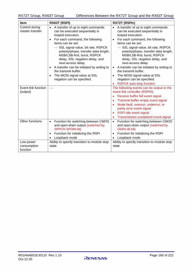
RX72T Group, RX63T Group Differences Between the RX72T Group and the RX63T Group
R01AN4651EJ0110 Rev.1.10 Page 160 of 222
Oct.12.20
Item RX63T (RSPI) RX72T (RSPIc)
Control during
master transfer • A transfer of up to eight commands
can be executed sequentially in
looped execution.
• For each command, the following
items can be set:
⎯ SSL signal value, bit rate, RSPCK
polarity/phase, transfer data length,
MSB/LSB-first, burst, RSPCK
delay, SSL negation delay, and
next-access delay
• A transfer can be initiated by writing to
the transmit buffer.
• The MOSI signal value at SSL
negation can be specified.
• A transfer of up to eight commands
can be executed sequentially in
looped execution.
• For each command, the following
items can be set:
⎯ SSL signal value, bit rate, RSPCK
polarity/phase, transfer data length,
MSB/LSB-first, burst, RSPCK
delay, SSL negation delay, and
next-access delay
• A transfer can be initiated by writing to
the transmit buffer.
• The MOSI signal value at SSL
negation can be specified.
• RSPCK auto-stop function
Event link function
(output)
⎯ The following events can be output to the
event link controller (RSPI0):
• Receive buffer full event signal
• Transmit buffer empty event signal
• Mode fault, overrun, underrun, or
parity error event signal
• RSPI idle event signal
• Transmission-completed event signal
Other functions • Function for switching between CMOS
and open-drain output (switched by
SPPCR.SPOM bit)
• Function for initializing the RSPI
• Loopback mode
• Function for switching between CMOS
and open-drain output (switched by
ODRn.Bi bit)
• Function for initializing the RSPI
• Loopback mode
Low power
consumption
function
Ability to specify transition to module stop
state
Ability to specify transition to module stop
state
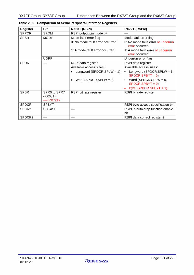
RX72T Group, RX63T Group Differences Between the RX72T Group and the RX63T Group
R01AN4651EJ0110 Rev.1.10 Page 161 of 222
Oct.12.20
Table 2.80 Comparison of Serial Peripheral Interface Registers
Register Bit RX63T (RSPI) RX72T (RSPIc)
SPPCR SPOM RSPI output pin mode bit ⎯
SPSR MODF Mode fault error flag
0: No mode fault error occurred.
1: A mode fault error occurred.
Mode fault error flag
0: No mode fault error or underrun
error occurred.
1: A mode fault error or underrun
error occurred.
UDRF ⎯ Underrun error flag
SPDR ⎯ RSPI data register
Available access sizes:
• Longword (SPDCR.SPLW = 1)
• Word (SPDCR.SPLW = 0)
RSPI data register
Available access sizes:
• Longword (SPDCR.SPLW = 1,
SPDCR.SPBYT = 0)
• Word (SPDCR.SPLW = 0,
SPDCR.SPBYT = 0)
• Byte (SPDCR.SPBYT = 1)
SPBR SPR0 to SPR7
(RX63T)
⎯ (RX72T)
RSPI bit rate register RSPI bit rate register
SPDCR SPBYT ⎯ RSPI byte access specification bit
SPCR2 SCKASE ⎯ RSPCK auto-stop function enable
bit
SPDCR2 ⎯ ⎯ RSPI data control register 2

RX72T Group, RX63T Group Differences Between the RX72T Group and the RX63T Group
R01AN4651EJ0110 Rev.1.10 Page 162 of 222
Oct.12.20
2.29 CRC Calculator
Table 2.81 is a comparative overview of CRC calculator, and Table 2.82 is a comparison of CRC calculator registers.
Table 2.81 Comparative Overview of CRC Calculator
Item RX63T (CRC) RX72T (CRCA)
Data size 8 bits 8 bits 32 bits
Data for CRC calculation
CRC codes are generated
8n-bit data units (where n
is a whole number).
CRC codes are generated
8n-bit data units (where n
is a whole number).
CRC codes are generated
32n-bit data units (where n
is a whole number).
CRC processing
method
8-bit parallel execution 8-bit parallel execution 32-bit parallel execution
CRC generation
polynomial
Ability to select among
three generation
polynomials
• 8-bit CRC
X8 + X2 + X + 1
• 16-bit CRC
X16 + X15 + X2 + 1,
X16 + X12 + X5 + 1
Ability to select among
three generation
polynomials
• 8-bit CRC
X8 + X2 + X + 1
• 16-bit CRC
X16 + X15 + X2 + 1,
X16 + X12 + X5 + 1
Ability to select among two
generation polynomials
• 32-bit CRC
X32 + X26 + X23 + X22
+ X16 + X12 + X11 + X10
+ X8 +X7 + X5 + X4 + X2
+ X + 1,
X32 + X28 + X27 + X26
+ X25 + X23 + X22 + X20
+ X19 + X18 + X14 + X13
+ X11 + X10 + X9 + X8
+ X6 + 1
CRC calculation
switching
Ability to select between
CRC code generation for
LSB-first or MSB-first
communication
The bit order of the CRC calculation result can be
switched to accommodate LSB-first or MSB-first for
communication.
Low power
consumption
function
Ability to specify transition
to module stop state
Ability to transition to module stop state

RX72T Group, RX63T Group Differences Between the RX72T Group and the RX63T Group
R01AN4651EJ0110 Rev.1.10 Page 163 of 222
Oct.12.20
Table 2.82 Comparison of CRC Calculator Registers
Register Bit RX63T (CRC) RX72T (CRCA)
CRCCR GPS[1:0] (RX63T)
GPS[2:0] (RX72T)
CRC generating polynomial
switching bits
(b1, b0)
b1 b0
0 0: No calculation
0 1: X8 + X2 + X + 1
1 0: X16 + X15 + X2 + 1
1 1: X16 + X12 + X5 + 1
CRC generating polynomial
switching bits
(b2 to b0)
b2 b0
0 0 0: No calculation
0 0 1: 8-bit CRC
(X8 + X2 + X + 1)
0 1 0: 16-bit CRC
(X16 + X15 + X2 + 1)
0 1 1: 16-bit CRC
(X16 + X12 + X5 + 1)
1 0 0: 32-bit CRC
(X32 + X26 + X23 + X22
+ X16 + X12 + X11 +X10
+ X8 + X7 + X5 + X4
+ X2 + X + 1)
1 0 1: 32-bit CRC
(X32 + X28 + X27 + X26
+ X25 + X23 + X22 +X20
+ X19 + X18 + X14 + X13
+ X11 + X10 + X9 + X8 + X6
+ 1)
1 1 0: No calculation
1 1 1: No calculation
LMS CRC calculation switching bit
(b2)
CRC calculation switching bit
(b6)
CRCDIR ⎯ CRC data input register
Available access sizes:
• Byte
CRC data input register
Available access sizes:
• Longword (for 32-bit CRC
generation)
• Byte (for 16-bit or 8-bit CRC
generation)
CRCDOR ⎯ CRC data output register
Available access sizes:
• Word
When generating 8-bit CRCs,
the lower-order byte (bits b7
to b0) is used.
CRC data output register
Available access sizes:
• Longword (for 32-bit CRC
generation)
• Word (for 16-bit CRC
generation)
• Byte (for 8-bit CRC
generation)
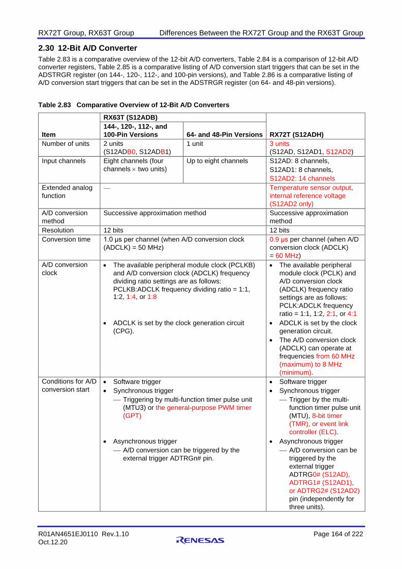
RX72T Group, RX63T Group Differences Between the RX72T Group and the RX63T Group
R01AN4651EJ0110 Rev.1.10 Page 164 of 222
Oct.12.20
2.30 12-Bit A/D Converter
Table 2.83 is a comparative overview of the 12-bit A/D converters, Table 2.84 is a comparison of 12-bit A/D converter registers, Table 2.85 is a comparative listing of A/D conversion start triggers that can be set in the ADSTRGR register (on 144-, 120-, 112-, and 100-pin versions), and Table 2.86 is a comparative listing of A/D conversion start triggers that can be set in the ADSTRGR register (on 64- and 48-pin versions).
Table 2.83 Comparative Overview of 12-Bit A/D Converters
Item
RX63T (S12ADB)
RX72T (S12ADH)
144-, 120-, 112-, and
100-Pin Versions 64- and 48-Pin Versions
Number of units 2 units
(S12ADB0, S12ADB1)
1 unit 3 units
(S12AD, S12AD1, S12AD2)
Input channels Eight channels (four
channels two units)
Up to eight channels S12AD: 8 channels,
S12AD1: 8 channels,
S12AD2: 14 channels
Extended analog
function
⎯ Temperature sensor output,
internal reference voltage
(S12AD2 only)
A/D conversion
method
Successive approximation method Successive approximation
method
Resolution 12 bits 12 bits
Conversion time 1.0 μs per channel (when A/D conversion clock
(ADCLK) = 50 MHz)
0.9 μs per channel (when A/D
conversion clock (ADCLK)
= 60 MHz)
A/D conversion
clock • The available peripheral module clock (PCLKB)
and A/D conversion clock (ADCLK) frequency
dividing ratio settings are as follows:
PCLKB:ADCLK frequency dividing ratio = 1:1, 1:2, 1:4, or 1:8
• The available peripheral
module clock (PCLK) and
A/D conversion clock
(ADCLK) frequency ratio
settings are as follows:
PCLK:ADCLK frequency
ratio = 1:1, 1:2, 2:1, or 4:1
• ADCLK is set by the clock generation circuit
(CPG).
• ADCLK is set by the clock
generation circuit.
• The A/D conversion clock
(ADCLK) can operate at
frequencies from 60 MHz
(maximum) to 8 MHz
(minimum).
Conditions for A/D
conversion start • Software trigger
• Synchronous trigger
⎯ Triggering by multi-function timer pulse unit
(MTU3) or the general-purpose PWM timer
(GPT)
• Software trigger
• Synchronous trigger
⎯ Trigger by the multi-
function timer pulse unit
(MTU), 8-bit timer
(TMR), or event link
controller (ELC).
• Asynchronous trigger
⎯ A/D conversion can be triggered by the
external trigger ADTRGn# pin.
• Asynchronous trigger
⎯ A/D conversion can be
triggered by the
external trigger
ADTRG0# (S12AD),
ADTRG1# (S12AD1),
or ADTRG2# (S12AD2)
pin (independently for
three units).

RX72T Group, RX63T Group Differences Between the RX72T Group and the RX63T Group
R01AN4651EJ0110 Rev.1.10 Page 165 of 222
Oct.12.20
Item
RX63T (S12ADB)
RX72T (S12ADH)
144-, 120-, 112-, and
100-Pin Versions 64- and 48-Pin Versions
Data registers • Eight registers for analog input, one for A/D-
converted data duplication in double-trigger
mode, and two for A/D-converted data duplication
during extended operation in double-trigger mode
• 30 registers (S12AD: 8,
S12AD1: 8, S12AD2: 14)
for analog input, one for
A/D-converted data
duplication in double
trigger mode per unit, and
two for A/D-converted data
duplication during
extended operation in
double trigger mode per
unit.
• One register for
temperature sensor
(S12AD2)
• One register for internal
reference voltage
(S12AD2)
• One register for self-
diagnosis per unit
• A/D conversion results are stored in 12-bit A/D
data registers.
• 8, 10, or 12-bit precision output of the results of
A/D conversion (selectable between 2 and 4-bit
right shift for output of conversion results)
• Accumulated A/D conversion results are stored
as a 14-bit value in A/D data registers in
cumulative mode.
• Double trigger mode (selectable in single cycle
scan or group scan mode)
⎯ The first piece of A/D-converted analog input
data on one selected channel is stored in the
data register for the channel, and the second
piece is stored in the duplication register.
• A/D conversion results are
stored in 12-bit A/D data
registers.
• In A/D-converted value
addition mode, the value
obtained by adding up A/D-
converted results is stored
as (conversion accuracy bit
count + 2 bits / 4 bits) in
the A/D data registers.
• Double trigger mode
(selectable in single scan
or group scan mode)
⎯ The first piece of A/D-
converted analog input
data on one selected
channel is stored in the
data register for the
channel, and the
second piece is stored
in the duplication
register.
• Extended operation in double trigger mode
(available for specific triggers)
⎯ A/D-converted analog input data on one
selected channel is stored in the duplication
register prepared for each trigger.
• Extended operation in
double trigger mode
(available for specific
triggers)
⎯ A/D-converted analog
input data on one
selected channel is
stored in the duplication
register prepared for
each trigger.

RX72T Group, RX63T Group Differences Between the RX72T Group and the RX63T Group
R01AN4651EJ0110 Rev.1.10 Page 166 of 222
Oct.12.20
Item
RX63T (S12ADB)
RX72T (S12ADH)
144-, 120-, 112-, and
100-Pin Versions 64- and 48-Pin Versions
Event link function ⎯ • An event signal is output
when all scans are
finished.
• An event signal is output
according to the
comparison function
window conditions in single
scan mode.
• Ability to start scanning by
a trigger from the ELC
Low power
consumption
function
Ability to specify transition to module stop state Ability to transition to module
stop state
Reference voltage
supply pin
VREFH0 AVCC0, AVCC1, AVCC2
Reference ground
pin
VREFL0 AVSS0, AVSS1, AVSS2
Functions • Sample-and-hold
function
• Channel-dedicated
sample-and-hold
function (three
channels per unit)
• Sample-and-hold
function
• Channel-dedicated
sample-and-hold
function (three
channels)
• Sample-and-hold function
• Channel-dedicated
sample-and-hold function
(three channels for S12AD
and three channels for
S12AD1) (ability to specify
constant sampling)
• Variable sampling
state count
• Variable sampling
state count
• Variable sampling time
function (ability to specify
on per channel basis)
• 12-bit A/D converter
self-diagnostic
function
• 12-bit A/D converter
self-diagnostic
function
• 12-bit A/D converter self-
diagnostic function
• A/D-converted value
addition mode
• A/D-converted value
addition mode
• Ability to select between
A/D-converted value
addition mode and average
mode
• Discharge function • Discharge function • Analog input disconnection
detection assist function
(discharge
function/precharge
function)
• Double trigger mode
(duplication of A/D
conversion data)
• Double trigger mode
(duplication of A/D
conversion data)
• Double trigger mode
(duplication of A/D
conversion data)
• Window-comparator
function (three
channels/unit)
• Window-comparator
function (three
channels/unit)
• For functionality equivalent
to the window comparator
function of RX63T, refer to
the Comparator C chapter
in RX72T Group User’s
Manual: Hardware.
• A/D data register
auto-clear function
• A/D data register
auto-clear function
• A/D data register auto-
clear function

RX72T Group, RX63T Group Differences Between the RX72T Group and the RX63T Group
R01AN4651EJ0110 Rev.1.10 Page 167 of 222
Oct.12.20
Item
RX63T (S12ADB)
RX72T (S12ADH)
144-, 120-, 112-, and
100-Pin Versions 64- and 48-Pin Versions
Functions • Comparison function
(windows A and B)
• Ability to specify order of
channel conversion for
each unit
• Input signal
amplification function
using programmable
gain amplifier (three
channels per unit)
• Input signal amplification
function using
programmable gain
amplifier (Each unit has
three channels; either
single-ended input or
pseudo-differential input
can be selected.)
Operating modes The operating mode can be
set independently for three
units.
• Single-cycle scan
mode:
⎯ A/D conversion is
performed only
once on the
analog inputs of
up to four
arbitrarily selected
channels.
• Single-cycle scan
mode:
⎯ A/D conversion is
performed only
once on the
analog inputs of
up to eight
arbitrarily selected
channels.
• Single scan mode:
⎯ A/D conversion is
performed only once on
arbitrarily selected
analog inputs.
⎯ A/D conversion is
performed only once on
the temperature sensor
output (S12AD2).
⎯ A/D conversion is
performed only once on
the internal reference
voltage (S12AD2).
• Continuous scan
mode:
⎯ A/D conversion is
performed
repeatedly on the
analog inputs of
up to four
arbitrarily selected
channels.
• Continuous scan
mode:
⎯ A/D conversion is
performed
repeatedly on the
analog inputs of
up to eight
arbitrarily selected
channels.
• Continuous scan mode:
⎯ A/D conversion is
performed repeatedly
on arbitrarily selected
analog inputs.
• Group scan mode: • Group scan mode: • Group scan mode:
⎯ Two (groups A and B)
or three (groups A, B,
and C) can be selected
as the number of the
groups to be used.
(Only the combination
of groups A and B can
be selected when the
number of the groups is
two.)

RX72T Group, RX63T Group Differences Between the RX72T Group and the RX63T Group
R01AN4651EJ0110 Rev.1.10 Page 168 of 222
Oct.12.20
Item
RX63T (S12ADB)
RX72T (S12ADH)
144-, 120-, 112-, and
100-Pin Versions 64- and 48-Pin Versions
Operating modes ⎯ Up to four
channels of analog
inputs are divided
between group A
and group B, and
A/D conversion is
performed only
once on all the
selected channels
on a group basis.
⎯ Up to eight
channels of analog
inputs are divided
between group A
and group B, and
A/D conversion is
performed only
once on all the
selected channels
on a group basis.
⎯ Analog inputs on
arbitrarily selected
channels, the
temperature sensor
output (S12AD2), and
the internal reference
voltage (S12AD2) are
divided into groups A
and B or into groups A,
B, and C, and A/D
conversion is performed
only once on the inputs
selected in group units.
⎯ The scan start
conditions of
group A and group
B can be selected
independently,
allowing A/D
conversion of
group A and group
B to be started at
different times.
⎯ The scan start
conditions of
group A and group
B can be selected
independently,
allowing A/D
conversion of
group A and group
B to be started at
different times.
⎯ The conditions for
starting scanning of
groups A, B, and C
(synchronous trigger)
can be selected
independently, allowing
A/D conversion of each
group to be started at
different times.
• Group scan mode
(when group A has
priority):
⎯ If a group A trigger
is input during A/D
conversion on
group B, A/D
conversion on
group B is stopped
and A/D
conversion is
performed on
group A.
⎯ After the A/D
conversion on
group A is
completed, A/D
conversion on
group B is
restarted (rescan).
• Group scan mode
(when group A has
priority):
⎯ If a group A trigger
is input during A/D
conversion on
group B, A/D
conversion on
group B is stopped
and A/D
conversion is
performed on
group A.
⎯ After the A/D
conversion on
group A is
completed, A/D
conversion on
group B is
restarted (rescan).
• Group scan mode (group
priority control selected):
⎯ If a higher-priority group
trigger is input during
scanning of a lower-
priority group, scan of
the lower-priority group
is stopped and scan of
the higher-priority group
is started. The priority
order is group A
(highest) > group B
> group C (lowest).
Whether or not to
restart scanning of
(rescan) the lower-
priority group after
processing for the
higher-priority group
completes, is
selectable. Rescan can
also be set to start
either from the first
selected channel or
from the channel on
which A/D conversion is
not completed.

RX72T Group, RX63T Group Differences Between the RX72T Group and the RX63T Group
R01AN4651EJ0110 Rev.1.10 Page 169 of 222
Oct.12.20
Item
RX63T (S12ADB)
RX72T (S12ADH)
144-, 120-, 112-, and
100-Pin Versions 64- and 48-Pin Versions
Interrupt sources • In modes other than
double trigger mode
and group scan
mode, a scan end
interrupt (S12ADI or
S12ADI1) request can
be generated on
completion of single
scan.
• In modes other than
double trigger mode
and group scan
mode, a scan end
interrupt (S12ADI)
request can be
generated on
completion of single
scan.
• In modes other than
double trigger mode and
group scan mode, a scan
end interrupt request
(S12ADI, S12ADI1, or
S12ADI2) can be
generated on completion of
single scan (independently
for each of three units).
• In double trigger
mode, a scan end
interrupt (S12ADI or
S12ADI1) request can
be generated on
completion of double
scan.
• In double trigger
mode, a scan end
interrupt (S12ADI)
request can be
generated on
completion of double
scan.
• In double trigger mode, a
scan end interrupt request
(S12ADI, S12ADI1, or
S12ADI2) can be
generated on completion of
double scan
(independently for each of
three units).
• In group scan mode,
a scan end interrupt
(S12ADI or S12ADI1)
request can be
generated on
completion of group A
scan, and a scan end
interrupt request
specially for group B
(S12GBADI or
S12GBADI1) can be
generated on
completion of group B
scan.
• In group scan mode,
a scan end interrupt
(S12ADI) request can
be generated on
completion of group A
scan, and a scan end
interrupt request
specially for group B
(S12GBADI) can be
generated on
completion of group B
scan.
• In group scan mode, a
scan end interrupt request
(S12ADI, S12ADI1, or
S12ADI2) can be
generated on completion of
group A scan, a group B
scan end interrupt request
(S12GBADI, S12GBADI1,
or S12GBADI2) can be
generated on completion of
group B scan, and a group
C scan end interrupt
request (S12GCADI,
S12GCADI1, or
S12GCADI2) can be
generated on completion of
group C scan.
• In group scan double
trigger mode, a scan
end interrupt (S12ADI
or S12ADI1) request
can be generated on
completion of double
scan of group A, and
a scan end interrupt
request specially for
group B (S12GBADI
or S12GBADI1) can
be generated on
completion of group B
scan.
• In group scan double
trigger mode, a scan
end interrupt
(S12ADI) request can
be generated on
completion of double
scan of group A, and
a scan end interrupt
request specially for
group B (S12GBADI)
can be generated on
completion of group B
scan.
• When double trigger group
scan mode is selected, a
scan end interrupt request
(S12ADI, S12ADI1, or
S12ADI2) can be
generated on completion of
double scan of group A,
and a corresponding scan
end interrupt request
(S12GBADI/S12GCADI,
S12GBADI1/S12GCADI1,
or S12GBADI2/
S12GCADI2) can be
generated on completion of
group B or group C scan.

RX72T Group, RX63T Group Differences Between the RX72T Group and the RX63T Group
R01AN4651EJ0110 Rev.1.10 Page 170 of 222
Oct.12.20
Item
RX63T (S12ADB)
RX72T (S12ADH)
144-, 120-, 112-, and
100-Pin Versions 64- and 48-Pin Versions
Interrupt sources • An interrupt request
(CMP0 to CMP2 or
CMP4 to CMP6) is
generated (and can
be used as a POE
source) in response
to detection by the
comparator.
• An interrupt request
(CMP0 to CMP2) is
generated (and can
be used as a POE
source) in response
to detection by the
comparator.
• A compare interrupt
request (S12CMPAI,
S12CMPAI1, S12CMPAI2,
S12CMPBI, S12CMPBI1,
or S12CMPBI2) can be
generated upon a match
with the comparison
condition of the digital
compare function.
• The S12ADI,
S12GBADI, S12ADI1,
S12GBADI1, CMP0
to CMP2, and CMP4
to CMP6 interrupts
can be used to
activate the DMA
controller (DMAC) or
the data-transfer
controller (DTC).
• The S12ADI,
S12GBADI, and
CMP0 to CMP2
interrupts can be
used to activate the
DMA controller
(DMAC) or the data-
transfer controller
(DTC).
• The S12ADI/S12ADI1/
S12ADI2, S12GBADI/
S12GBADI1/S12GBADI2,
and S12GCADI/
S12GCADI1/S12GCADI2
interrupts can trigger the
DMA controller (DMAC)
and data transfer controller
(DTC).

RX72T Group, RX63T Group Differences Between the RX72T Group and the RX63T Group
R01AN4651EJ0110 Rev.1.10 Page 171 of 222
Oct.12.20
Table 2.84 Comparison of 12-Bit A/D Converter Registers
Register Bit
RX63T (S12ADA)
144-, 120-, 112-, and
100-Pin Versions
64- and 48-Pin
Versions RX72T (S12ADH)
ADDRy ⎯ A/D data register y
(y = 0 to 3)
A/D data register y
(y = 0 to 7)
A/D data register y
(y = 0 to 7: S12AD,
y = 0 to 7: S12AD1,
y = 0 to 11, 16, 17: S12AD2)
ADRD AD[11:0]
(RX63T)
⎯ (RX72T)
12-bit A/D-converted value 12-bit A/D-converted value
DIAGST[1:0]
(RX63T)
⎯ (RX72T)
Self-diagnostic status bits Self-diagnostic status bits
ADANSA ⎯ A/D channel select register A ⎯
ADANSB ⎯ A/D channel select register B ⎯
ADADS ⎯ A/D-converted value addition mode select
register
⎯
ADADC ADC[1:0]
(RX63T)
ADC[2:0]
(RX72T)
Addition count select bits Addition count select bits
AVEE ⎯ Average mode enable bit
ADCER ADPRC[1:0] A/D data-register bit-precision specification
bits
⎯
DCE DCE discharge enable bit ⎯
ADRFMT A/D data register format select bit A/D data register format select
bit
When A/D-converted value addition mode is
selected, the format of each data register is
fixed to left-alignment, regardless of the
setting of the ADCER.ADRFMT bit.
⎯
ADSTRGR TRSB[5:0]
(RX63T: 144-,
120-, 112- and
100-pin
versions,
RX72T)
TRSB[4:0]
(RX63T: 64- and
48-pin versions)
A/D conversion start trigger select for group B
bits
Refer to Table 2.85 and Table 2.86 for details.
A/D conversion start trigger
select for group B bits
Refer to Table 2.85 and Table
2.86 for details.
TRSA[5:0]
(RX63T: 144-,
120-, 112- and
100-pin
versions,
RX72T)
TRSA[4:0]
(RX63T: 64- and
48-pin versions)
A/D conversion start trigger select bits
Refer to Table 2.85 and Table 2.86 for details.
A/D conversion start trigger
select bits
Refer to Table 2.85 and Table
2.86 for details.

RX72T Group, RX63T Group Differences Between the RX72T Group and the RX63T Group
R01AN4651EJ0110 Rev.1.10 Page 172 of 222
Oct.12.20
Register Bit
RX63T (S12ADA)
144-, 120-, 112-, and
100-Pin Versions
64- and 48-Pin
Versions RX72T (S12ADH)
ADSSTRn SST[7:0]
(RX63T)
⎯ (RX72T)
A/D sampling state
register n (n = 0 to 3)
A/D sampling state
register n (n = 0 to 7)
A/D sampling state register n
(n = 0 to 11, L, T, or O)
The valid setting range is 13 to 255 states. Specify the value for the
register as a multiple of 3 in the
range from 12 to 252 (clock
cycles).
Initial values after a reset are different.
ADSHCR SSTSH[7:0] Sampling time sample-and-hold circuit setting
bits
Channel-dedicated sample-
and-hold circuit sampling time
setting bits
The valid setting range is 4 to 255 states. Specify the value for the
register in the range from 12 to
252 (clock cycles).
Initial values after a reset are different.
ADGSPCR LGRRS ⎯ Restart channel select bit
ADCMPMD0 ⎯ Comparator operating-mode selection register
0
⎯
ADCMPMD1 ⎯ Comparator operating-mode selection register
1
⎯
ADCMPNR0 ⎯ Comparator filter-mode register 0 ⎯
ADCMPFR ⎯ Comparator detection flag register ⎯
ADCMPSEL ⎯ Comparator interrupt selection register ⎯
ADPG ⎯ A/D programmable
gain amplifier register
⎯ ⎯
ADGSPMR ⎯ A/D group scan
priority control
register
⎯ ⎯
ADTSDR ⎯ ⎯ A/D temperature sensor data
register
ADOCDR ⎯ ⎯ A/D internal reference voltage
data register
ADANSA0 ⎯ ⎯ A/D channel select register A0
ADANSA1 ⎯ ⎯ A/D channel select register A1
ADANSB0 ⎯ ⎯ A/D channel select register B0
ADANSB1 ⎯ ⎯ A/D channel select register B1
ADANSC0 ⎯ ⎯ A/D channel select register C0
ADANSC1 ⎯ ⎯ A/D channel select register C1
ADSCSn ⎯ ⎯ A/D channel conversion order
setting register n (n = 0 to 13)
ADADS0 ⎯ ⎯ A/D-converted value
addition/average function
channel select register 0
ADADS1 ⎯ ⎯ A/D-converted value
addition/average function
channel select register 1
ADEXICR ⎯ ⎯ A/D conversion extended input
control register
ADGCEXCR ⎯ ⎯ A/D group C extended input
control register
ADGCTRGR ⎯ ⎯ A/D group C trigger select
register

RX72T Group, RX63T Group Differences Between the RX72T Group and the RX63T Group
R01AN4651EJ0110 Rev.1.10 Page 173 of 222
Oct.12.20
Register Bit
RX63T (S12ADA)
144-, 120-, 112-, and
100-Pin Versions
64- and 48-Pin
Versions RX72T (S12ADH)
ADSHMSR ⎯ ⎯ A/D sample-and-hold operating
mode select register
ADDISCR ⎯ ⎯ A/D disconnection detection
control register
ADELCCR ⎯ ⎯ A/D event link control register
ADCMPCR ⎯ ⎯ A/D comparison function
control register
ADCMPANSR0 ⎯ ⎯ A/D comparison function
window A channel select
register 0
ADCMPANSR1 ⎯ ⎯ A/D comparison function
window A channel select
register 1
ADCMPANSER ⎯ ⎯ A/D comparison function
window A extended input select
register
ADCMPLR0 ⎯ ⎯ A/D comparison function
window A comparison condition
setting register 0
ADCMPLR1 ⎯ ⎯ A/D comparison function
window A comparison condition
setting register 1
ADCMPLER ⎯ ⎯ A/D comparison function
window A extended input
comparison condition setting
register
ADCMPDR0 ⎯ ⎯ A/D comparison function
window A lower level setting
register
ADCMPDR1 ⎯ ⎯ A/D comparison function
window A upper level setting
register
ADCMPSR0 ⎯ ⎯ A/D comparison function
window A channel status
register 0
ADCMPSR1 ⎯ ⎯ A/D comparison function
window A channel status
register 1
ADCMPSER ⎯ ⎯ A/D comparison function
window A extended input
channel status register
ADWINMON ⎯ ⎯ A/D comparison function
window A/B status monitoring
register
ADCMPBNSR ⎯ ⎯ A/D comparison function
window B channel select
register
ADWINLLB ⎯ ⎯ A/D comparison function
window B lower level setting
register

RX72T Group, RX63T Group Differences Between the RX72T Group and the RX63T Group
R01AN4651EJ0110 Rev.1.10 Page 174 of 222
Oct.12.20
Register Bit
RX63T (S12ADA)
144-, 120-, 112-, and
100-Pin Versions
64- and 48-Pin
Versions RX72T (S12ADH)
ADWINULB ⎯ ⎯ A/D comparison function
window B upper level setting
register
ADCMPBSR ⎯ ⎯ A/D comparison function
window B channel status
register
ADPGACR ⎯ ⎯ A/D programmable gain
amplifier control register
ADPGAGS0 ⎯ ⎯ A/D programmable gain
amplifier gain setting register 0
ADPGADCR0 ⎯ ⎯ A/D programmable gain
amplifier differential input
control register
ADVMONCR ⎯ ⎯ A/D internal reference voltage
monitoring circuit enable
register
ADVMONO ⎯ ⎯ A/D internal reference voltage
monitoring circuit output enable
register

RX72T Group, RX63T Group Differences Between the RX72T Group and the RX63T Group
R01AN4651EJ0110 Rev.1.10 Page 175 of 222
Oct.12.20
Table 2.85 Comparison of A/D Conversion Start Triggers Set in ADSTRGR Register
(144-, 120-, 112-, and 100-Pin Versions)
Bit RX63T (S12ADB) RX72T (S12ADH)
TRSB[5:0] Group B A/D conversion start trigger select bits
b5 b0
1 1 1 1 1 1: No trigger source selected state
0 0 0 0 0 1: TRGA0N
0 0 0 0 1 0: TRGA1N
0 0 0 0 1 1: TRGA2N
0 0 0 1 0 0: TRGA3N
0 0 0 1 0 1: TRGA4N
0 0 0 1 1 0: TRGA6N
0 0 0 1 1 1: TRGA7N
0 0 1 0 0 0: TRG0AN
0 0 1 0 0 1: TRG4AN
0 0 1 0 1 0: TRG4BN
0 0 1 0 1 1: TRG4AN or TRG4BN
0 0 1 1 0 0: TRG4ABN
0 0 1 1 0 1: TRG7AN
0 0 1 1 1 0: TRG7BN
0 0 1 1 1 1: TRG7AN or TRG7BN
0 1 0 0 0 0: TRG7ABN
0 1 0 0 0 1: GTADTRA0N
0 1 0 0 1 0: GTADTRB0N
0 1 0 0 1 1: GTADTRA1N
0 1 0 1 0 0: GTADTRB1N
0 1 0 1 0 1: GTADTRA2N
0 1 0 1 1 0: GTADTRB2N
0 1 0 1 1 1: GTADTRA3N
0 1 1 0 0 0: GTADTRB3N
0 1 1 0 0 1: GTADTRA0N or GTADTRB0N
0 1 1 0 1 0: GTADTRA1N or GTADTRB1N
0 1 1 0 1 1: GTADTRA2N or GTADTRB2N
0 1 1 1 0 0: GTADTRA3N or GTADTRB3N
0 1 1 1 0 1: GTADTRA4N
0 1 1 1 1 0: GTADTRB4N
0 1 1 1 1 1: GTADTRA5N
1 0 0 0 0 0: GTADTRB5N
1 0 0 0 0 1: GTADTRA6N
1 0 0 0 1 0: GTADTRB6N
1 0 0 0 1 1: GTADTRA7N
1 0 0 1 0 0: GTADTRB7N
1 0 0 1 0 1: GTADTRA4N or GTADTRB4N
1 0 0 1 1 0: GTADTRA5N or GTADTRB5N
1 0 0 1 1 1: GTADTRA6N or GTADTRB6N
1 0 1 0 0 0: GTADTRA7N or GTADTRB7N
Group B A/D conversion start trigger select bits
b5 b0
1 1 1 1 1 1: No trigger source selected state
0 0 0 0 0 1: TRGA0N
0 0 0 0 1 0: TRGA1N
0 0 0 0 1 1: TRGA2N
0 0 0 1 0 0: TRGA3N
0 0 0 1 0 1: TRGA4N
0 0 0 1 1 0: TRGA6N
0 0 0 1 1 1: TRGA7N
0 0 1 0 0 0: TRG0N
0 0 1 0 0 1: TRG4AN
0 0 1 0 1 0: TRG4BN
0 0 1 0 1 1: TRG4AN or TRG4BN
0 0 1 1 0 0: TRG4ABN
0 0 1 1 0 1: TRG7AN
0 0 1 1 1 0: TRG7BN
0 0 1 1 1 1: TRG7AN or TRG7BN
0 1 0 0 0 0: TRG7ABN
0 1 0 0 1 1: TRGA9N
0 1 0 1 0 0: TRG9N
0 1 1 0 0 1: TRGA0N or TRG0N
0 1 1 0 1 0: TRGA9N or TRG9N
0 1 1 0 1 1: TRGA0N or TRGA9N
0 1 1 1 0 0: TRG0N or TRG9N
0 1 1 1 0 1: TMTRG0AN_0
0 1 1 1 1 0: TMTRG0AN_1
0 1 1 1 1 1: TMTRG0AN_2
1 0 0 0 0 0: TMTRG0AN_3
1 0 0 0 0 1: TRG9AEN
1 0 0 0 1 0: TRG0AEN
1 0 0 0 1 1: TRGA09N
1 0 0 1 0 0: TRG09N
1 1 0 0 1 0: ELCTRG00N*1/ELCTRG10N*2/
ELCTRG20N*3
1 1 0 0 1 1: ELCTRG01N*1/ELCTRG11N*2/ ELCTRG21N*3
1 1 1 0 1 0: ELCTRG00N or ELCTRG01N*1 ELCTRG10N or ELCTRG11N*2 ELCTRG20N or ELCTRG21N*3

RX72T Group, RX63T Group Differences Between the RX72T Group and the RX63T Group
R01AN4651EJ0110 Rev.1.10 Page 176 of 222
Oct.12.20
Bit RX63T (S12ADB) RX72T (S12ADH)
TRSA[5:0] A/D conversion start trigger select bits
b13 b8
1 1 1 1 1 1: No trigger source selected state
0 0 0 0 0 0: ADTRGn#
0 0 0 0 0 1: TRGA0N
0 0 0 0 1 0: TRGA1N
0 0 0 0 1 1: TRGA2N
0 0 0 1 0 0: TRGA3N
0 0 0 1 0 1: TRGA4N
0 0 0 1 1 0: TRGA6N
0 0 0 1 1 1: TRGA7N
0 0 1 0 0 0: TRG0AN
0 0 1 0 0 1: TRG4AN
0 0 1 0 1 0: TRG4BN
0 0 1 0 1 1: TRG4AN or TRG4BN
0 0 1 1 0 0: TRG4ABN
0 0 1 1 0 1: TRG7AN
0 0 1 1 1 0: TRG7BN
0 0 1 1 1 1: TRG7AN or TRG7BN
0 1 0 0 0 0: TRG7ABN
0 1 0 0 0 1: GTADTRA0N
0 1 0 0 1 0: GTADTRB0N
0 1 0 0 1 1: GTADTRA1N
0 1 0 1 0 0: GTADTRB1N
0 1 0 1 0 1: GTADTRA2N
0 1 0 1 1 0: GTADTRB2N
0 1 0 1 1 1: GTADTRA3N
0 1 1 0 0 0: GTADTRB3N
0 1 1 0 0 1: GTADTRA0N or GTADTRB0N
0 1 1 0 1 0: GTADTRA1N or GTADTRB1N
0 1 1 0 1 1: GTADTRA2N or GTADTRB2N
0 1 1 1 0 0: GTADTRA3N or GTADTRB3N
0 1 1 1 0 1: GTADTRA4N
0 1 1 1 1 0: GTADTRB4N
0 1 1 1 1 1: GTADTRA5N
1 0 0 0 0 0: GTADTRB5N
1 0 0 0 0 1: GTADTRA6N
1 0 0 0 1 0: GTADTRB6N
1 0 0 0 1 1: GTADTRA7N
1 0 0 1 0 0: GTADTRB7N
1 0 0 1 0 1: GTADTRA4N or GTADTRB4N
1 0 0 1 1 0: GTADTRA5N or GTADTRB5N
1 0 0 1 1 1: GTADTRA6N or GTADTRB6N
1 0 1 0 0 0: GTADTRA7N or GTADTRB7N
A/D conversion start trigger select bits
b13 b8
1 1 1 1 1 1: No trigger source selected state
0 0 0 0 0 0: ADTRGn#
0 0 0 0 0 1: TRGA0N
0 0 0 0 1 0: TRGA1N
0 0 0 0 1 1: TRGA2N
0 0 0 1 0 0: TRGA3N
0 0 0 1 0 1: TRGA4N
0 0 0 1 1 0: TRGA6N
0 0 0 1 1 1: TRGA7N
0 0 1 0 0 0: TRG0N
0 0 1 0 0 1: TRG4AN
0 0 1 0 1 0: TRG4BN
0 0 1 0 1 1: TRG4AN or TRG4BN
0 0 1 1 0 0: TRG4ABN
0 0 1 1 0 1: TRG7AN
0 0 1 1 1 0: TRG7BN
0 0 1 1 1 1: TRG7AN or TRG7BN
0 1 0 0 0 0: TRG7ABN
0 1 0 0 1 1: TRGA9N
0 1 0 1 0 0: TRG9N
0 1 1 0 0 1: TRGA0N or TRG0N
0 1 1 0 1 0: TRGA9N or TRG9N
0 1 1 0 1 1: TRGA0N or TRGA9N
0 1 1 1 0 0: TRG0N or TRG9N
0 1 1 1 0 1: TMTRG0AN_0
0 1 1 1 1 0: TMTRG0AN_1
0 1 1 1 1 1: TMTRG0AN_2
1 0 0 0 0 0: TMTRG0AN_3
1 0 0 0 0 1: TRG9AEN
1 0 0 0 1 0: TRG0AEN
1 0 0 0 1 1: TRGA09N
1 0 0 1 0 0: TRG09N
1 1 0 0 1 0: ELCTRG00N*1/ELCTRG10N*2/ ELCTRG20N*3
1 1 0 0 1 1: ELCTRG01N*1/ELCTRG11N*2/ ELCTRG21N*3
1 1 1 0 1 0: ELCTRG00N or ELCTRG01N*1 ELCTRG10N or ELCTRG11N*2 ELCTRG20N or ELCTRG21N*3
Notes: 1. Unit 0
2. Unit 1
3. Unit 2

RX72T Group, RX63T Group Differences Between the RX72T Group and the RX63T Group
R01AN4651EJ0110 Rev.1.10 Page 177 of 222
Oct.12.20
Table 2.86 Comparison of A/D Conversion Start Triggers Set in ADSTRGR Register
(64- and 48-Pin Versions)
Bit RX63T (S12ADB) RX72T (S12ADH)
TRSB[4:0]
(RX63T)
TRSB[5:0]
(RX72T)
Group B A/D conversion start trigger select bits
b4 b0
1 1 1 1 1: No trigger source selected state
0 0 0 0 1: TRGA0N
0 0 0 1 0: TRGA1N
0 0 0 1 1: TRGA2N
0 0 1 0 0: TRGA3N
0 0 1 0 1: TRGA4N
0 0 1 1 0: TRGA6N
0 0 1 1 1: TRGA7N
Group B A/D conversion start trigger select bits
b5 b0
1 1 1 1 1 1: No trigger source selected state
0 0 0 0 0 1: TRGA0N
0 0 0 0 1 0: TRGA1N
0 0 0 0 1 1: TRGA2N
0 0 0 1 0 0: TRGA3N
0 0 0 1 0 1: TRGA4N
0 0 0 1 1 0: TRGA6N
0 0 0 1 1 1: TRGA7N
0 1 0 0 0: TRG0AN
0 1 0 0 1: TRG4AN
0 1 0 1 0: TRG4BN
0 1 0 1 1: TRG4AN or TRG4BN
0 1 1 0 0: TRG4ABN
0 1 1 0 1: TRG7AN
0 1 1 1 0: TRG7BN
0 1 1 1 1: TRG7AN or TRG7BN
1 0 0 0 0: TRG7ABN
1 0 0 0 1: GTADTRA0N
1 0 0 1 0: GTADTRB0N
1 0 0 1 1: GTADTRA1N
1 0 1 0 0: GTADTRB1N
1 0 1 0 1: GTADTRA2N
1 0 1 1 0: GTADTRB2N
1 0 1 1 1: GTADTRA3N
1 1 0 0 0: GTADTRB3N
1 1 0 0 1: GTADTRA0N or GTADTRB0N
1 1 0 1 0: GTADTRA1N or GTADTRB1N
1 1 0 1 1: GTADTRA2N or GTADTRB2N
1 1 1 0 0: GTADTRA3N or GTADTRB3N
0 0 1 0 0 0: TRG0N
0 0 1 0 0 1: TRG4AN
0 0 1 0 1 0: TRG4BN
0 0 1 0 1 1: TRG4AN or TRG4BN
0 0 1 1 0 0: TRG4ABN
0 0 1 1 0 1: TRG7AN
0 0 1 1 1 0: TRG7BN
0 0 1 1 1 1: TRG7AN or TRG7BN
0 1 0 0 0 0: TRG7ABN
0 1 0 0 1 1: TRGA9N
0 1 0 1 0 0: TRG9N
0 1 1 0 0 1: TRGA0N or TRG0N
0 1 1 0 1 0: TRGA9N or TRG9N
0 1 1 0 1 1: TRGA0N or TRGA9N
0 1 1 1 0 0: TRG0N or TRG9N
0 1 1 1 0 1: TMTRG0AN_0
0 1 1 1 1 0: TMTRG0AN_1
0 1 1 1 1 1: TMTRG0AN_2
1 0 0 0 0 0: TMTRG0AN_3
1 0 0 0 0 1: TRG9AEN
1 0 0 0 1 0: TRG0AEN
1 0 0 0 1 1: TRGA09N
1 0 0 1 0 0: TRG09N
1 1 0 0 1 0: ELCTRG00N*1/ELCTRG10N*2/
ELCTRG20N*3
1 1 0 0 1 1: ELCTRG01N*1/ELCTRG11N*2/ ELCTRG21N*3
1 1 1 0 1 0: ELCTRG00N or ELCTRG01N*1 ELCTRG10N or ELCTRG11N*2 ELCTRG20N or ELCTRG21N*3

RX72T Group, RX63T Group Differences Between the RX72T Group and the RX63T Group
R01AN4651EJ0110 Rev.1.10 Page 178 of 222
Oct.12.20
Bit RX63T (S12ADB) RX72T (S12ADH)
TRSA[4:0]
(RX63T)
TRSA[5:0]
(RX72T)
A/D conversion start trigger select bits
b12 b8
1 1 1 1 1: No trigger source selected state
0 0 0 0 0: ADTRG0#
0 0 0 0 1: TRGA0N
0 0 0 1 0: TRGA1N
0 0 0 1 1: TRGA2N
0 0 1 0 0: TRGA3N
0 0 1 0 1: TRGA4N
0 0 1 1 0: TRGA6N
0 0 1 1 1: TRGA7N
0 1 0 0 0: TRG0AN
0 1 0 0 1: TRG4AN
0 1 0 1 0: TRG4BN
0 1 0 1 1: TRG4AN or TRG4BN
0 1 1 0 0: TRG4ABN
0 1 1 0 1: TRG7AN
0 1 1 1 0: TRG7BN
0 1 1 1 1: TRG7AN or TRG7BN
1 0 0 0 0: TRG7ABN
1 0 0 0 1: GTADTRA0N
1 0 0 1 0: GTADTRB0N
1 0 0 1 1: GTADTRA1N
1 0 1 0 0: GTADTRB1N
1 0 1 0 1: GTADTRA2N
1 0 1 1 0: GTADTRB2N
1 0 1 1 1: GTADTRA3N
1 1 0 0 0: GTADTRB3N
1 1 0 0 1: GTADTRA0N or GTADTRB0N
1 1 0 1 0: GTADTRA1N or GTADTRB1N
1 1 0 1 1: GTADTRA2N or GTADTRB2N
1 1 1 0 0: GTADTRA3N or GTADTRB3N
A/D conversion start trigger select bits
b13 b8
1 1 1 1 1 1: No trigger source selected state
0 0 0 0 0 0: ADTRGn#
0 0 0 0 0 1: TRGA0N
0 0 0 0 1 0: TRGA1N
0 0 0 0 1 1: TRGA2N
0 0 0 1 0 0: TRGA3N
0 0 0 1 0 1: TRGA4N
0 0 0 1 1 0: TRGA6N
0 0 0 1 1 1: TRGA7N
0 0 1 0 0 0: TRG0N
0 0 1 0 0 1: TRG4AN
0 0 1 0 1 0: TRG4BN
0 0 1 0 1 1: TRG4AN or TRG4BN
0 0 1 1 0 0: TRG4ABN
0 0 1 1 0 1: TRG7AN
0 0 1 1 1 0: TRG7BN
0 0 1 1 1 1: TRG7AN or TRG7BN
0 1 0 0 0 0: TRG7ABN
0 1 0 0 1 1: TRGA9N
0 1 0 1 0 0: TRG9N
0 1 1 0 0 1: TRGA0N or TRG0N
0 1 1 0 1 0: TRGA9N or TRG9N
0 1 1 0 1 1: TRGA0N or TRGA9N
0 1 1 1 0 0: TRG0N or TRG9N
0 1 1 1 0 1: TMTRG0AN_0
0 1 1 1 1 0: TMTRG0AN_1
0 1 1 1 1 1: TMTRG0AN_2
1 0 0 0 0 0: TMTRG0AN_3
1 0 0 0 0 1: TRG9AEN
1 0 0 0 1 0: TRG0AEN
1 0 0 0 1 1: TRGA09N
1 0 0 1 0 0: TRG09N
1 1 0 0 1 0: ELCTRG00N*1/ELCTRG10N*2/ ELCTRG20N*3
1 1 0 0 1 1: ELCTRG01N*1/ELCTRG11N*2/ ELCTRG21N*3
1 1 1 0 1 0: ELCTRG00N or ELCTRG01N*1 ELCTRG10N or ELCTRG11N*2 ELCTRG20N or ELCTRG21N*3
Notes: 1. Unit 0
2. Unit 1
3. Unit 2

RX72T Group, RX63T Group Differences Between the RX72T Group and the RX63T Group
R01AN4651EJ0110 Rev.1.10 Page 179 of 222
Oct.12.20
2.31 D/A Converter
Table 2.87 is a comparative overview of the D/A converters, and Table 2.88 is a comparison of D/A converter registers.
Table 2.87 Comparative Overview of D/A Converters
Item RX63T (DAa) RX72T (R12DAb)
Resolution 10 bits 12 bits
Output channels 2 channels 2 channels
Measure against
interference between
analog modules
Measure against interference between
D/A and A/D conversion:
D/A-converted data update timing is
controlled by the 10-bit A/D converter
synchronous D/A conversion enable
input signal from the 10-bit A/D
converter. (Degradation of A/D
conversion accuracy caused by
interference is reduced by controlling
the D/A converter inrush current
generation timing with the enable
signal).
Measure against interference between
D/A and A/D conversion:
D/A-converted data update timing is
controlled by the 12-bit A/D converter
synchronous D/A conversion enable
signal from the 12-bit A/D converter
(unit 2).
Therefore, degradation of A/D
conversion accuracy due to interference
is reduced by controlling the timing at
which the 12-bit D/A converter inrush
current occurs, with the enable signal.
Low power
consumption function
Ability to specify transition to module
stop state
Ability to transition to module stop state
Event link function
(input)
⎯ Ability to start D/A conversion on
channel 0 when an event signal is input
Output destination
selection
⎯ Ability to control output to external pins
and to comparator C independently
Reference voltage
supply pin
AVCC AVCC2
Reference ground pin AVSS AVSS2
Table 2.88 Comparison of D/A Converter Registers
Register Bit RX63T (DAa) RX72T (R12DAb)
DADSELR ⎯ ⎯ D/A destination select register
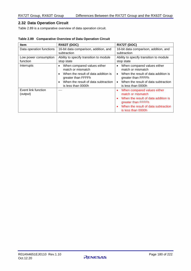
RX72T Group, RX63T Group Differences Between the RX72T Group and the RX63T Group
R01AN4651EJ0110 Rev.1.10 Page 180 of 222
Oct.12.20
2.32 Data Operation Circuit
Table 2.89 is a comparative overview of data operation circuit.
Table 2.89 Comparative Overview of Data Operation Circuit
Item RX63T (DOC) RX72T (DOC)
Data operation functions 16-bit data comparison, addition, and
subtraction
16-bit data comparison, addition, and
subtraction
Low power consumption
function
Ability to specify transition to module
stop state
Ability to specify transition to module
stop state
Interrupts • When compared values either
match or mismatch
• When the result of data addition is
greater than FFFFh
• When the result of data subtraction
is less than 0000h
• When compared values either
match or mismatch
• When the result of data addition is
greater than FFFFh
• When the result of data subtraction
is less than 0000h
Event link function
(output)
⎯ • When compared values either
match or mismatch
• When the result of data addition is
greater than FFFFh
• When the result of data subtraction
is less than 0000h

RX72T Group, RX63T Group Differences Between the RX72T Group and the RX63T Group
R01AN4651EJ0110 Rev.1.10 Page 181 of 222
Oct.12.20
2.33 RAM
Table 2.90 is a comparative overview of RAM, and Table 2.91 is a comparison of RAM registers.
Table 2.90 Comparative Overview of RAM
Item RX63T (RAM)
RX72T
Without ECC Error
Correction (RAM)
With ECC Error Correction
(ECCRAM)
Capacity • 48 KB
• 32 KB
• 24 KB
• 8 KB
128 KB 16 KB
Address • 0000 0000h to 0000
BFFFh (48 KB)
• 0000 0000h to 0000
7FFFh (32 KB)
• 0000 0000h to 0000
5FFFh (24 KB)
• 0000 0000h to 0000
1FFFh (8 KB)
0000 0000h to 0001 FFFFh 00FF C000h to 00FF FFFFh
Memory bus Memory bus 1 Memory bus 1 Memory bus 3
Access • Single-cycle access is
possible for both
reading and writing.
• On-chip RAM can be
enabled or disabled.
• Single-cycle access is
possible for both reading
and writing.
• RAM can be enabled or
disabled.
• The ECC function can be
enabled or disabled.
[When MEMWAIT = 0]
• The ECC function is
disabled: Access takes
two cycles for reading or
writing.
• The ECC function is
enabled (when no error
has occurred): Access
takes two cycles for
reading or writing.
• The ECC function is
enabled (when an error
has occurred): Access
takes three cycles for
reading or writing.

RX72T Group, RX63T Group Differences Between the RX72T Group and the RX63T Group
R01AN4651EJ0110 Rev.1.10 Page 182 of 222
Oct.12.20
Item RX63T (RAM)
RX72T
Without ECC Error
Correction (RAM)
With ECC Error Correction
(ECCRAM)
Access [When MEMWAIT = 1]
• The ECC function is
disabled: Access takes
three cycles for reading or
writing.
• The ECC function is
enabled (when no error
has occurred): Reading
takes three cycles and
writing takes four cycles.
• The ECC function is
enabled (when an error
has occurred): Access
takes five cycles for
reading or writing.
Data retention
function
Not available in deep
software standby mode
Not available in deep software standby mode
Low power
consumption
function
Ability to specify transition
to module stop state
Transition to module stop state can be enabled separately
for RAM and ECCRAM.
Error checking — • Detection of 1-bit errors
• A non-maskable
interrupt or interrupt is
generated in response
to an error.
• ECC error correction:
Correction of 1-bit errors
and detection of 2-bit
errors
• A non-maskable interrupt
or interrupt is generated in
response to an error.
Table 2.91 Comparison of RAM Registers
Register Bit RX63T (RAM) RX72T (RAM, ECCRAM)
ECCRAMMODE — — ECCRAM operating mode control
register
ECCRAM2STS — — ECCRAM 2-bit error status register
ECCRAM1STSEN — — ECCRAM 1-bit error information
update enable register
ECCRAM1STS — — ECCRAM 1-bit error status register
ECCRAMPRCR — — ECCRAM protection register
ECCRAM2ECAD — — ECCRAM 2-bit error address
capture register
ECCRAM1ECAD — — ECCRAM 1-bit error address
capture register
ECCRAMPRCR2 — — ECCRAM protection register 2
ECCRAMETST — — ECCRAM test control register
RAMMODE — — RAM operating mode control
register
RAMSTS — — RAM error status register
RAMECAD — — RAM error address capture register
RAMPRCR — — RAM protection register

RX72T Group, RX63T Group Differences Between the RX72T Group and the RX63T Group
R01AN4651EJ0110 Rev.1.10 Page 183 of 222
Oct.12.20
2.34 Flash Memory
Table 2.92 is a comparative overview of flash memory, and Table 2.93 is a comparison of flash memory registers.
Table 2.92 Comparative Overview of Flash Memory
Item
RX63T RX72T
ROM E2 DataFlash
Code Flash
Memory
Data Flash
Memory
Memory
capacity • User area:
512 KB, 384 KB,
256 KB, 64 KB,
48 KB, 32 KB
• User boot area:
16 KB
Data area:
32 KB or 8 KB • User area:
1 MB, 512 KB
• User boot area:
32 KB
Data area:
32 KB
Address [User area]
• Capacity of
32 KB
FFFF 8000h to
FFFF FFFFh
• Capacity of
48 KB
FFFF 4000h to
FFFF FFFFh
• Capacity of
64 KB
FFFF 0000h to
FFFF FFFFh
• Capacity of
256 KB
FFFC 0000h to
FFFF FFFFh
• Capacity of
384 KB
FFFA 0000h to
FFFF FFFFh
• Capacity of
32 KB
0010 0000h to
0010 7FFFh
• Capacity of
8 KB
0010 0000h to
0010 1FFFh
[User area] 0010 0000h to
0010 7FFFh
• Capacity of
512 KB
FFF8 0000h to
FFFF FFFFh
[User boot area]
FF7F C000h to
FF7F FFFFh
• Capacity of
512 KB
FFF8 0000h to
FFFF FFFFh
• Capacity of
1 MB
FFF0 0000h to
FFFF FFFFh
[User boot area]
FF7F 8000h to
FF7F FFFFh
ROM cache — • Capacity: 8 KB
• Mapping
method:
direct mapping
• Line size:
16 bytes
—

RX72T Group, RX63T Group Differences Between the RX72T Group and the RX63T Group
R01AN4651EJ0110 Rev.1.10 Page 184 of 222
Oct.12.20
Item
RX63T RX72T
ROM E2 DataFlash
Code Flash
Memory
Data Flash
Memory
Read cycle A read operation
takes one cycle of
ICLK.
A read operation
takes six cycles of
FCLK for word or
byte access.
• While ROM
cache operation
is enabled:
When the cache is hit, one cycle;
when the cache is missed:
⎯ One to two
cycles if ICLK
≤ 120 MHz
⎯ Two to three
cycles if ICLK
> 120 MHz
• When ROM
cache operation
is disabled:
⎯ One cycle if
ICLK ≤
120 MHz
⎯ Two cycles if
ICLK >
120 MHz
A read operation
takes eight cycles of
FCLK for 16-bit or
8-bit access.
Value after
erasure
FFh Undefined FFh Undefined
Programming/
erasing
method
• The chip incorporates a dedicated
sequencer (FCU) for programming the
ROM/E2 DataFlash.
• Programming and erasing the ROM/E2
DataFlash are handled by issuing
commands to the FCU.
• A dedicated sequencer (FCU) is
incorporated for programming the flash
memory.
• Programming and erasing the code
flash memory/data flash memory are
handled using FACI commands
specified in the FACI command issuing
area (007E 0000h).
• Programming/erasure through transfer
by a flash-memory programmer via a
serial interface (serial programming)
• Programming/erasure of flash memory
by a user program (self-programming)
Security
function
Protects against illicit tampering or reading
of data in flash memory
Protects against illicit tampering or reading
of data in flash memory
Protection
function
Protects against erroneous rewriting of the
flash memory (software protection, error
protection, and boot program protection)
Protects against erroneous rewriting of the
flash memory (software protection, error
protection, and boot program protection)
Trusted
memory (TM)
function
— Protects against illicit reading of blocks 8
and 9 in the code flash memory
Background
operation
(BGO)
The CPU is able to execute program code
from the ROM while the E2 DataFlash
memory is being programmed or erased.
The user area can be read while the data
area is being programmed or erased.

RX72T Group, RX63T Group Differences Between the RX72T Group and the RX63T Group
R01AN4651EJ0110 Rev.1.10 Page 185 of 222
Oct.12.20
Item
RX63T RX72T
ROM E2 DataFlash
Code Flash
Memory
Data Flash
Memory
Suspension
and
resumption
• The CPU is able to execute program
code from the ROM during suspension
of programming or erasure.
• The CPU is able to execute program
code from the E2 DataFlash during
suspension of programming or erasure.
• Programming and erasure of the
ROM/E2 DataFlash can be restarted
(resumed) after suspension.
—
Units of
programming
and erasure
• Unit of
programming for
the user area or
user boot area:
128 bytes
• Unit of erasure
for the user area:
Block
• Unit of erasure
for the user boot
area: 16 KB (Not
present in 64-
and 48-pin
products.)
• Unit of
programming for
the data area:
2 bytes
• Unit of erasure
for the data area:
Block
• Unit of
programming for
the user area or
user boot area:
256 bytes
• Unit of erasure
for the user area:
Block
• Unit of
programming for
the data area:
4 bytes
• Unit of erasure
for the data area:
Block
Blank checking — • The blank
checking
command can be
executed to
check the
erasure state of
the data flash.
— • The blank
checking
command can be
executed to
check the
erasure state of
the data flash.
• The size of the
area to be blank-
checked is 2
bytes or 2 KB.
• The size of the
area to be blank-
checked is 4
bytes to 32
Kbytes (specifed
in 4-byte
increments).
Other functions Interrupts can be accepted during self-
programming.
Interrupts can be accepted during self-
programming.

RX72T Group, RX63T Group Differences Between the RX72T Group and the RX63T Group
R01AN4651EJ0110 Rev.1.10 Page 186 of 222
Oct.12.20
Item
RX63T RX72T
ROM E2 DataFlash
Code Flash
Memory
Data Flash
Memory
On-board
programming
(serial
programming/
self-
programming)
• Programming in boot mode
⎯ The asynchronous serial interface
(SCI1) is used.
⎯ The transfer rate is adjusted
automatically.
⎯ The user boot area can also be
programmed.
• Programming in USB boot mode (Not
supported on 112-, 100-, 64-, and 48-
pin products.)
⎯ USB0 is used.
⎯ Dedicated hardware is not required,
so direct connection to a PC is
possible.
• Programming in the user boot mode
(Not supported on 64- and 48-pin
products.)
⎯ Support for original boot programs
created by the user.
• Programming by a routine for ROM/E2
DataFlash programming within the user
program
⎯ Allows ROM/E2 DataFlash
programming without resetting the
system.
• Programming/erasure in boot mode (for
the SCI interface)
⎯ The asynchronous serial interface
(SCI1) is used.
⎯ The transfer rate is adjusted
automatically.
⎯ The user boot area can also be
programmed or erased.
• Programming/erasure in boot mode
(USB interface)
⎯ USBb is used.
⎯ Dedicated hardware is not required,
so direct connection to a PC is
possible.
• Programming/erasure in boot mode
(FINE interface)
⎯ FINE is used.
• Programming/erasure in user boot
mode
⎯ Support for original boot programs
created by the user.
• Programming/erasure by self-
programming
⎯ Allows user area/data area
programming and erasure without
resetting the system.
Off-board
programming
(programming
and erasure
using parallel
programmer)
A flash programmer
can be used to
program the user
area and user boot
area.
A flash programmer
cannot be used to
program the data
area.
Programming and
erasure of the user
area and user boot
area by a parallel
programmer is
possible.
Programming or
erasure of the data
area by a parallel
programmer is not
possible.
Unique ID — A 12-byte ID code provided for each MCU
Table 2.93 Comparison of Flash Memory Registers
Register Bit RX63T RX72T
FMODR — Flash mode register —
FASTAT DFLWPE E2 DataFlash
programming/erasure
protection violation flag
—
DFLRPE E2 DataFlash read protection
violation flag
—
DFLAE (RX63T)
DFAE (RX72T)
E2 DataFlash access violation
flag
Data flash memory access
violation flag
ROMAE (RX63T)
CFAE (RX72T)
ROM access violation flag Code flash memory access
violation flag

RX72T Group, RX63T Group Differences Between the RX72T Group and the RX63T Group
R01AN4651EJ0110 Rev.1.10 Page 187 of 222
Oct.12.20
Register Bit RX63T RX72T
FAEINT DFLWPEIE E2 DataFlash
programming/erasure
protection violation interrupt
enable bit
—
DFLRPEIE E2 DataFlash read protection
violation interrupt enable bit
—
DFLAEIE (RX63T)
DFAEIE (RX72T)
E2 DataFlash access violation
interrupt enable bit
Data flash memory access
violation interrupt enable bit
ROMAEIE (RX63T)
CFAEIE (RX72T)
ROM access violation interrupt
enable bit
Code flash memory access
violation interrupt enable bit
DFLRE0 — E2 DataFlash read enable
register 0
—
DFLRE1 — E2 DataFlash read enable
register 1
—
DFLWE0 — E2 DataFlash P/E enable
register 0
—
DFLWE1 — E2 DataFlash P/E enable
register 1
—
FSTATR0
(RX63T)
FSTATR
(RX72T)
FLWEERR — Flash write/erase protect error
flag
PRGSPD Programming suspend status
flag (b0)
Programming suspend status
flag (b8)
ERSSPD Erasure suspend status flag
(b1)
Erasure suspend status flag
(b9)
DBFULL — Data Buffer Full Flag
SUSRDY Suspend ready flag (b3) Suspend ready flag (b11)
PRGERR Programming error flag (b4) Programming error flag (b12)
ERSERR Erasure error bit (b5) Erasure error flag (b13)
ILGLERR Illegal command error flag (b6) Illegal error command flag (b14)
FRDY Flash ready flag (b7) Flash ready flag (b15)
FSTATR1 — Flash status register 1 —
FENTRYR FENTRY0(RX63T)
FENTRYC(RX72T)
ROM P/E mode entry bit 0 Code flash memory P/E mode
entry bit
FEKEY[7:0]
(RX63T)
KEY[7:0](RX72T)
Key code bit Key code bit
FPROTR FPKEY[7:0]
(RX63T)
KEY[7:0](RX72T)
Key code bit Key code bit
FRESETR — Flash reset register —
DFLBCCNT — E2 DataFlash blank check
control register
—
DFLBCSTAT
(RX63T)
FBCSTAT
(RX72T)
BCST Blank check status bit
DFLBCSTAT is a 16-bit
register.
Blank check status flag
FBCSTAT is an 8-bit register.

RX72T Group, RX63T Group Differences Between the RX72T Group and the RX63T Group
R01AN4651EJ0110 Rev.1.10 Page 188 of 222
Oct.12.20
Register Bit RX63T RX72T
PCKAR
(RX63T)
FPCKAR
(RX72T)
PCKA[7:0] Peripheral clock notification bits
These bits are used to set the
FlashIF clock (FCLK) at
programming/erasure of the
ROM/E2 DataFlash.
Flash sequencer processing
clock frequency notification bits
These bits are used to set the
frequency of the FlashIF clock
(FCLK) and notify the flash
sequencer of the frequency
used.
KEY[7:0] — Key code bits
ROMCE — — ROM cache enable register
ROMCIV — — ROM cache invalidate register
NCRGn — — Non-cacheable area n address
register (n = 0 or 1)
NCRCn — — Non-cacheable area n setting
register (n = 0 or 1)
FSADDR — — FACI command processing start
address register
FEADDR — — FACI command processing end
address register
FSUINITR — — Flash sequencer set-up
initialization register
FLKSTAT — — Lock bit status register
FBCCNT — — Data flash blank check control
register
FPSADDR — — Data flash programming start
address register
UIDRn — — Unique ID register n (n = 0 to 2)
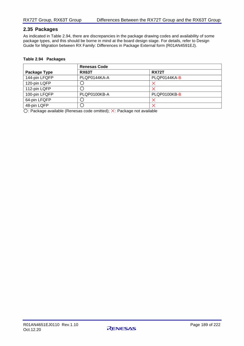
RX72T Group, RX63T Group Differences Between the RX72T Group and the RX63T Group
R01AN4651EJ0110 Rev.1.10 Page 189 of 222
Oct.12.20
2.35 Packages
As indicated in Table 2.94, there are discrepancies in the package drawing codes and availability of some package types, and this should be borne in mind at the board design stage. For details, refer to Design Guide for Migration between RX Family: Differences in Package External form (R01AN4591EJ).
Table 2.94 Packages
Package Type
Renesas Code
RX63T RX72T
144-pin LFQFP PLQP0144KA-A PLQP0144KA-B
120-pin LQFP 112-pin LQFP 100-pin LFQFP PLQP0100KB-A PLQP0100KB-B
64-pin LFQFP 48-pin LQFP
: Package available (Renesas code omitted); : Package not available

RX72T Group, RX63T Group Differences Between the RX72T Group and the RX63T Group
R01AN4651EJ0110 Rev.1.10 Page 190 of 222
Oct.12.20
3. Comparison of Pin Functions
This section presents a comparative description of pin functions as well as a comparison of the pins for the
power supply, clocks, and system control. Items that exist only on one group are indicated by blue text. Items
that exists on both groups with different specifications are indicated by red text. Black text indicates there is
no differences in the item’s specifications between groups.
3.1 144-Pin Package (RX72T: With PGA Pseudo-Differential Input and USB Pins)
Table 3.1 is a comparative listing of the pin functions of 144-pin package products.
Table 3.1 Comparative Listing of 144-Pin Package Pin Functions
144 Pins RX63T
RX72T
(With PGA Pseudo-Differential Input and
USB Pin)
1 VCC_USB P14/MTIOC4B/MTIOC4B#/GTIOC2A/
GTIOC9A/GTIOC2A#/GTIOC9A#/IRQ11
2 PE5/BCLK/USB0_VBUS/IRQ0 P13/MTIOC4A/MTIOC4A#/GTIOC1A/
GTIOC8A/GTIOC1A#/GTIOC8A#/IRQ10
3 EMLE P12/MTIOC3B/MTIOC3B#/GTIOC0A/
GTIOC7A/GTIOC0A#/GTIOC7A#/IRQ9
4 TRSYNC/P03/RXD2/SMISO2/SSCL2/IRQ7 PE6/RD#/GTETRGA/GTETRGB/
GTETRGC/GTETRGD/POE10#/IRQ3
5 TRDATA3/P02/TXD2/SMOSI2/SSDA2 PE5/BCLK/MTIOC9D/MTIOC9D#/
GTIOC3A/GTETRGB/GTIOC3A#/
GTETRGD/SCK9/CTS9#/RTS9#/SS9#/
IRQ0/ADST0
6 VSS VCC
7 P01/RD#/CTS0#/RTS0#/SS0#/USB0_DRPD EMLE
8 VCL VSS
9 P00/CS1#/CACREF UB/P00/A11/MTIOC9A/MTIOC9A#/
CACREF/RXD9/SMISO9/SSCL9/RXD12/
SMISO12/SSCL12/RXDX12/IRQ2/ADST1/
COMP0
10 MD/FINED VCL
11 PE4/A10/POE10#/MTCLKC/IRQ1 MD/FINED
12 PE3/A11/POE11#/MTCLKD/IRQ2-DS P01/A10/MTIOC9C/MTIOC9C#/GTETRGA/
GTETRGB/GTETRGC/GTETRGD/
POE12#/TXD9/SMOSI9/SSDA9/TXD12/
SMOSI12/SSDA12/TXDX12/SIOX12/IRQ4/
ADST2/COMP1
13 TRDATA2/P14/SCK2 PE4/A9/MTCLKC/MTCLKC#/GTETRGA/
GTETRGB/GTETRGC/GTETRGD/POE10#/
SCK9/IRQ1
14 VCC PE3/A8/MTCLKD/MTCLKD#/GTETRGA/
GTETRGB/GTETRGC/GTETRGD/
POE11#/CTS9#/RTS9#/SS9#/IRQ2_DS
15 P13/CTS2#/RTS2#/SS2#/USB0_VBUSEN RES#
16 RES# XTAL/P37
17 XTAL VSS
18 VSS EXTAL/P36
19 EXTAL VCC
20 VCC UPSEL/PE2/POE10#/NMI

RX72T Group, RX63T Group Differences Between the RX72T Group and the RX63T Group
R01AN4651EJ0110 Rev.1.10 Page 191 of 222
Oct.12.20
144 Pins RX63T
RX72T
(With PGA Pseudo-Differential Input and
USB Pin)
21 PE2/POE10#/NMI PE1/WR0#/WR#/MTIOC9D/MTIOC9D#/
TMO5/CTS5#/RTS5#/SS5#/CTS12#/
RTS12#/SS12#/SSLA3/IRQ15
22 PE1/WR0#/WR#/CTS12#/RTS12#/SS12#/
SSLA3/SSLB3/USB0_OVRCURA
PE0/WR1#/BC1#/WAIT#/MTIOC9B/
MTIOC9B#/TMCI1/TMCI5/RXD5/SMISO5/
SSCL5/SSLA2/CRX0/USB0_OVRCURB/
IRQ7
23 PE0/WR1#/BC1#/WAIT#/SSLA2/SSLB2/
CRX1/USB0_OVRCURB/IRQ7
TRST#/PD7/MTIOC9A/MTIOC9A#/
GTIOC0A/GTIOC3A/GTIOC0A#/GTIOC3A#/
TMRI1/TMRI5/TXD5/SMOSI5/SSDA5/
SSLA1/CTX0/IRQ8
24 PD7/GTIOC0A/CTS0#/RTS0#/SS0#/SSLA1/
SSLB1/CTX1
TMS/PD6/MTIOC9C/MTIOC9C#/GTIOC0B/
GTIOC3B/GTIOC0B#/GTIOC3B#/TMO1/
CTS1#/RTS1#/SS1#/CTS11#/RTS11#/
SS11#/SSLA0/IRQ5/ADST0
25 PD6/GTIOC0B/SSLA0/SSLB0 TDI/PD5/GTIOC1A/GTETRGA/GTIOC1A#/
TMRI0/TMRI6/RXD1/SMISO1/SSCL1/
RXD11/SMISO11/SSCL11/IRQ6
26 PD5/GTIOC1A/RXD1/SMISO1/SSCL1/IRQ6 TCK/PD4/GTIOC1B/GTETRGB/
GTIOC1B#/TMCI0/TMCI6/SCK1/SCK11/
IRQ2
27 VSS TDO/PD3/GTIOC2A/GTETRGC/GTIOC2A#/
TMO0/TXD1/SMOSI1/SSDA1/TXD11/
SMOSI11/SSDA11
28 PD4/GTIOC1B/SCK1 TRCLK/PD2/A7/GTIOC2B/GTIOC0A/
GTIOC2B#/GTIOC0A#/TMCI1/TMO4/
SCK5/SCK8/MOSIA/USB0_VBUS
29 PD3/GTIOC2A/TXD1/SMOSI1/SSDA1 TRDATA3/PD1/A6/GTIOC3A/GTIOC0B/
GTIOC3A#/GTIOC0B#/TMO2/RXD8/
SMISO8/SSCL8/MISOA
30 PD2/CS2#/GTIOC2B/MOSIA/MOSIB/
USB0_ID
TRDATA2/PD0/A5/GTIOC3B/GTIOC1A/
GTIOC3B#/GTIOC1A#/TMO6/TXD8/
SMOSI8/SSDA8/RSPCKA
31 PD1/CS0#/GTIOC3A/MISOA/MISOB/
USB0_EXICEN
TRDATA7/PF3/A19/CS3#/GTETRGA/
TMO7/CTS11#/RTS11#/SS11#/CRX0/
IRQ14/COMP0
32 PD0/A12/GTIOC3B/RSPCKA/RSPCKB TRDATA6/PF2/A18/CS2#/GTETRGB/
TMO3/SCK11/CTX0/IRQ5/COMP1
33 PF4/CS3# TRDATA5/PF1/A17/CS1#/GTETRGC/
TMO5/RXD11/SMISO11/SSCL11/IRQ13/
COMP2
34 PF3/TXD1/SMOSI1/SSDA1 TRDATA4/PF0/A0/BC0#/GTETRGD/TMO1/
TXD11/SMOSI11/SSDA11/IRQ12/COMP3
35 PF2/CS1#/RXD1/SMISO1/SSCL1/IRQ5 USB0_DM
36 TRST#/PF1 USB0_DP
37 TMS/PF0 VSS_USB
38 PB7/A19/SCK12 VCC_USB
39 PB6/A18/RXD12/SMISO12/SSCL12/
RXDX12/CRX1/IRQ2
TRDATA1/PB7/A4/GTIOC1B/GTIOC1B#/
SCK5/SCK11/SCK12/USB0_OVRCURB

RX72T Group, RX63T Group Differences Between the RX72T Group and the RX63T Group
R01AN4651EJ0110 Rev.1.10 Page 192 of 222
Oct.12.20
144 Pins RX63T
RX72T
(With PGA Pseudo-Differential Input and
USB Pin)
40 PB5/A17/TXD12/SMOSI12/SSDA12/
TXDX12/SIOX12/CTX1
TRDATA0/PB6/A3/GTIOC2A/GTIOC2A#/
RXD5/SMISO5/SSCL5/RXD11/SMISO11/
SSCL11/RXD12/SMISO12/SSCL12/
RXDX12/CRX0/USB0_OVRCURA/IRQ2
41 PLLVCC TRSYNC/PB5/A2/GTIOC2B/GTIOC2B#/
TXD5/SMOSI5/SSDA5/TXD11/SMOSI11/
SSDA11/TXD12/SMOSI12/SSDA12/
TXDX12/SIOX12/CTX0/USB0_VBUSEN
42 PB4/A16/POE8#/GTETRG0/IRQ3-DS VCC
43 PLLVSS TRSYNC1/PB4/A1/GTETRGA/GTETRGB/
GTETRGC/GTETRGD/POE8#/CTS5#/
RTS5#/SS5#/SCK11/CTS11#/RTS11#/
SS11#/USB0_OVRCURB/IRQ3_DS
44 TDI/RXD1*1 VSS
45 TCK/FINEC PC2/CS1#/MTIOC0D/MTIOC0D#/
GTADSM0/SCK8/USB0_ID/
USB0_OVRCURA/IRQ15/ADSM0/COMP5
46 TDO/TXD1*1 PC1/A16/MTIOC0C/MTIOC0C#/GTADSM1/
TXD8/SMOSI8/SSDA8/USB0_EXICEN/
USB0_VBUSEN/IRQ13/ADSM1/COMP4
47 PB3/A15/MTIOC0A/CACREF/SCK0 PC0/CS0#/MTIOC0B/MTIOC0B#/RXD8/
SMISO8/SSCL8/USB0_VBUS/IRQ12/
COMP3
48 PB2/MTIOC0B/TXD0/SMOSI0/SSDA0/
SDA0
PB3/A7/MTIOC0A/MTIOC0A#/CACREF/
SCK6/RSPCKA/IRQ9
49 PB1/MTIOC0C/RXD0/SMISO0/SSCL0/
SCL0/IRQ4
PB2/A6/MTIOC0B/MTIOC0B#/GTADSM0/
TMRI0/TXD6/SMOSI6/SSDA6/SDA/ADSM0
50 PB0/A14/MTIOC0D/MOSIA/MOSIB PB1/A5/MTIOC0C/MTIOC0C#/GTADSM1/
TMCI0/RXD6/SMISO6/SSCL6/SCL/IRQ4/
ADSM1
51 TRDATA1/PA6/CS3#/CTS3#/RTS3#/SS3# PB0/A0/BC0#/A4/MTIOC0D/MTIOC0D#/
TMO0/TXD6/SMOSI6/SSDA6/CTS11#/
RTS11#/SS11#/MOSIA/IRQ8/ADTRG2#
52 PA5/MTIOC1A/RXD0/SMISO0/SSCL0/
MISOA/MISOB/ADTRG1#
PA7/A15/MTCLKA/MTCLKC/MTCLKA#/
MTCLKC#/GTADSM0/TMO2/RXD11/
SMISO11/SSCL11/RXD12/SMISO12/
SSCL12/RXDX12/CRX0/ADSM0
53 PA4/MTIOC1B/TXD0/SMOSI0/SSDA0/
RSPCKA/RSPCKB/ADTRG0#
PA6/A14/MTCLKB/MTCLKD/MTCLKB#/
MTCLKD#/GTADSM1/TMO6/TXD11/
SMOSI11/SSDA11/TXD12/SMOSI12/
SSDA12/TXDX12/SIOX12/CTX0/IRQ7/
ADSM1
54 PA3/MTIOC2A/SCK0/SSLA0/SSLB0 PA5/A3/MTIOC1A/MTIOC1A#/TMCI3/
RXD6/SMISO6/SSCL6/RXD8/SMISO8/
SSCL8/MISOA/IRQ1/ADTRG1#
55 PA2/MTIOC2B/RXD2/SMISO2/SSCL2/
SSLA1/SSLB1
PA4/A2/MTIOC1B/MTIOC1B#/TMCI7/
SCK6/TXD8/SMOSI8/SSDA8/RSPCKA/
ADTRG0#
56 PA1/MTIOC6A/TXD2/SMOSI2/SSDA2/
SSLA2/SSLB2
PA3/A1/MTIOC2A/MTIOC2A#/GTADSM0/
TMRI7/TXD9/SMOSI9/SSDA9/SCK8/SSLA0

RX72T Group, RX63T Group Differences Between the RX72T Group and the RX63T Group
R01AN4651EJ0110 Rev.1.10 Page 193 of 222
Oct.12.20
144 Pins RX63T
RX72T
(With PGA Pseudo-Differential Input and
USB Pin)
57 PA0/MTIOC6C/SCK2/SSLA3/SSLB3 PA2/A0/BC0#/MTIOC2B/MTIOC2B#/
GTADSM1/TMO7/CTS6#/RTS6#/SS6#/
RXD9/SMISO9/SSCL9/SCK11/SSLA1
58 TRDATA0/P35/TXD3/SMOSI3/SSDA3 PA1/MTIOC6A/MTIOC6A#/TMO4/TXD9/
SMOSI9/SSDA9/RXD11/SMISO11/SSCL11/
SSLA2/CRX0/USB0_ID/USB0_OVRCURA/
IRQ14_DS/ADTRG0#
59 TRCLK/P34/GTETRG1/RXD3/SMISO3/
SSCL3/IRQ3
PA0/MTIOC6C/MTIOC6C#/TMO2/SCK9/
TXD11/SMOSI11/SSDA11/SSLA3/CTX0/
USB0_EXICEN/USB0_VBUSEN
60 VCC P35/A13/MTIOC2A/MTIOC9A/MTIOC2A#/
MTIOC9A#/GTADSM0/TMO0/CTS8#/
RTS8#/SS8#/TXD1/SMOSI1/SSDA1/IRQ6
61 P96/A13/POE4#/RXD1/SMISO1/SSCL1/
IRQ4-DS
P34/A12/MTIOC2B/MTIOC9B/MTIOC2B#/
MTIOC9B#/GTADSM1/GTETRGB/TMO4/
CTS9#/RTS9#/SS9#/RXD1/SMISO1/SSCL1/
USB0_OVRCURB/IRQ3
62 PG6/CS2#/SCK1 PC6/MTIOC1A/MTIOC9C/MTIOC1A#/
MTIOC9C#/RXD11/SMISO11/SSCL11/
CRX0/IRQ11_DS
63 VSS PC5/MTIOC1B/MTIOC9D/MTIOC1B#/
MTIOC9D#/TXD11/SMOSI11/SSDA11/
CTX0/IRQ10_DS
64 P95/MTIOC6B/GTIOC4A/TXD1/SMOSI1/
SSDA1
VCC
65 P94/MTIOC7A/GTIOC5A/CTS1#/RTS1#/
SS1#
P96/CS0#/WAIT#/GTETRGA/GTETRGB/
GTETRGC/GTETRGD/POE4#/CTS8#/
RTS8#/SS8#/IRQ4_DS
66 P93/MTIOC7B/GTIOC6A/CTS2#/RTS2#/
SS2#
VSS
67 P92/MTIOC6D/GTIOC4B P95/MTIOC6B/MTIOC6B#/GTIOC4A/
GTIOC7A/GTIOC4A#/GTIOC7A#
68 P91/MTIOC7C/GTIOC5B P94/MTIOC7A/MTIOC7A#/GTIOC5A/
GTIOC8A/GTIOC5A#/GTIOC8A#
69 P90/MTIOC7D/GTIOC6B P93/MTIOC7B/MTIOC7B#/GTIOC6A/
GTIOC9A/GTIOC6A#/GTIOC9A#
70 PG5/POE12#/SCK3/ADTRG# P92/MTIOC6D/MTIOC6D#/GTIOC4B/
GTIOC7B/GTIOC4B#/GTIOC7B#
71 PG4/GTIOC6B/RXD3/SMISO3/SSCL3/IRQ6 P91/MTIOC7C/MTIOC7C#/GTIOC5B/
GTIOC8B/GTIOC5B#/GTIOC8B#
72 PG3/GTIOC6A/TXD3/SMOSI3/SSDA3 P90/MTIOC7D/MTIOC7D#/GTIOC6B/
GTIOC9B/GTIOC6B#/GTIOC9B#
73 PG2/SCK2/IRQ2 P76/D0[A0/D0]/MTIOC4D/MTIOC4D#/
GTIOC2B/GTIOC6B/GTIOC2B#/GTIOC6B#
74 PG1/GTIOC7B/RXD2/SMISO2/SSCL2/IRQ1 P75/D1[A1/D1]/MTIOC4C/MTIOC4C#/
GTIOC1B/GTIOC5B/GTIOC1B#/GTIOC5B#
75 PG0/GTIOC7A/TXD2/SMOSI2/SSDA2/IRQ0 P74/D2[A2/D2]/MTIOC3D/MTIOC3D#/
GTIOC0B/GTIOC4B/GTIOC0B#/GTIOC4B#
76 P76/D0[A0/D0]/MTIOC4D/GTIOC2B P73/D3[A3/D3]/MTIOC4B/MTIOC4B#/
GTIOC2A/GTIOC6A/GTIOC2A#/GTIOC6A#

RX72T Group, RX63T Group Differences Between the RX72T Group and the RX63T Group
R01AN4651EJ0110 Rev.1.10 Page 194 of 222
Oct.12.20
144 Pins RX63T
RX72T
(With PGA Pseudo-Differential Input and
USB Pin)
77 P75/D1[A1/D1]/MTIOC4C/GTIOC1B P72/D4[A4/D4]/MTIOC4A/MTIOC4A#/
GTIOC1A/GTIOC5A/GTIOC1A#/GTIOC5A#
78 P74/D2[A2/D2]/MTIOC3D/GTIOC0B P71/D5[A5/D5]/MTIOC3B/MTIOC3B#/
GTIOC0A/GTIOC4A/GTIOC0A#/GTIOC4A#
79 P73/D3[A3/D3]/MTIOC4B/GTIOC2A P70/D6[A6/D6]/GTETRGA/GTETRGB/
GTETRGC/GTETRGD/POE0#/CTS9#/
RTS9#/SS9#/IRQ5_DS
80 P72/D4[A4/D4]/MTIOC4A/GTIOC1A PG2/D11[A11/D11]/GTETRGA/GTIOC0B/
GTIOC0B#/SCK9/IRQ2/COMP0
81 P71/D5[A5/D5]/MTIOC3B/GTIOC0A PG1/D12[A12/D12]/GTIOC0A/GTIOC0A#/
TXD9/SMOSI9/SSDA9/IRQ1/COMP1
82 P70/D6[A6/D6]/POE0#/CTS1#/RTS1#/
SS1#/IRQ5-DS
PG0/D13[A13/D13]/GTIOC1B/GTIOC1B#/
RXD9/SMISO9/SSCL9/IRQ0/COMP2
83 P33/D7[A7/D7]/MTIOC3A/MTCLKA/
SSLA3/SSLB3
PK2/D14[A14/D14]/GTIOC1A/GTIOC1A#/
POE12#/CTS9#/RTS9#/SS9#/SCK5/
IRQ9_DS/COMP3
84 P32/D8[A8/D8]/MTIOC3C/MTCLKB/
SSLA2/SSLB2
PK1/D15[A15/D15]/GTIOC2B/GTIOC2B#/
POE13#/CTS8#/RTS8#/SS8#/TXD5/
SMOSI5/SSDA5/IRQ8_DS/COMP4
85 VCC PK0/CS1#/GTIOC2A/GTIOC2A#/POE14#/
RXD5/SMISO5/SSCL5/IRQ15_DS/COMP5
86 P31/D9[A9/D9]/MTIOC0A/MTCLKC/
SSLA1/SSLB1
P33/D7[A7/D7]/MTIOC3A/MTCLKA/
MTIOC3A#/MTCLKA#/GTIOC3B/GTIOC3B#/
TMO0/SSLA3/IRQ13_DS
87 VSS P32/D8[A8/D8]/MTIOC3C/MTCLKB/
MTIOC3C#/MTCLKB#/GTIOC3A/
GTIOC3A#/TMO6/SSLA2/IRQ12_DS
88 P30/D10[A10/D10]/MTIOC0B/MTCLKD/
SCK0/SSLA0/SSLB0
VCC
89 P26/CS0#/TXD1/SMOSI1/SSDA1/SDA1 P31/D9[A9/D9]/MTIOC0A/MTCLKC/
MTIOC0A#/MTCLKC#/TMRI6/SSLA1/IRQ6
90 P25/CS1#/SCK1/SCL1 VSS
91 P24/D11[A11/D11]/CTS0#/RTS0#/SS0#/
RSPCKA/RSPCKB/IRQ4
P30/D10[A10/D10]/MTIOC0B/MTCLKD/
MTIOC0B#/MTCLKD#/TMCI6/SCK8/CTS8#/
RTS8#/SS8#/SSLA0/IRQ7/COMP3
92 P23/D12[A12/D12]/CACREF/TXD0/
SMOSI0/SSDA0/MOSIA/MOSIB/CTX1
P27/CS3#/MTIOC1A/MTIOC0C/MTIOC1A#/
MTIOC0C#/POE9#/IRQ15
93 P22/D13[A13/D13]/RXD0/SMISO0/SSCL0/
MISOA/MISOB/CRX1/ADTRG#
P26/CS2#/MTIOC9A/MTIOC9A#/CTS1#/
RTS1#/SS1#/IRQ11/ADST0
94 P21/D14[A14/D14]/MTCLKA/IRQ6-DS/
ADTRG1#
P25/CS3#/MTIOC9C/MTIOC9C#/SCK1/
IRQ10/ADST1
95 P20/D15[A15/D15]/MTCLKB/IRQ7-DS/
ADTRG0#
P24/D11[A11/D11]/MTIC5U/MTIC5U#/
TMCI2/TMO6/CTS8#/RTS8#/SS8#/SCK8/
RSPCKA/IRQ4/COMP0
96 PC5/AN19 P23/D12[A12/D12]/MTIC5V/MTIC5V#/
TMO2/CACREF/TXD8/SMOSI8/SSDA8/
TXD12/SMOSI12/SSDA12/TXDX12/SIOX12/
MOSIA/CTX0/IRQ11/COMP1

RX72T Group, RX63T Group Differences Between the RX72T Group and the RX63T Group
R01AN4651EJ0110 Rev.1.10 Page 195 of 222
Oct.12.20
144 Pins RX63T
RX72T
(With PGA Pseudo-Differential Input and
USB Pin)
97 PC4/AN18 P22/D13[A13/D13]/MTIC5W/MTCLKD/
MTIC5W#/MTCLKD#/MTIOC9B/TMRI2/
TMO4/RXD8/SMISO8/SSCL8/RXD12/
SMISO12/SSCL12/RXDX12/MISOA/CRX0/
IRQ10/ADTRG2#/COMP2
98 P65/A0/BC0#/AN5 PC4/A20/MTIOC9B/MTIOC9B#/TXD1/
SMOSI1/SSDA1/TXD12/SMOSI12/SSDA12/
TXDX12/SIOX12/ADST2/COMP5
99 P64/A1/AN4 PC3/MTIOC9D/MTIOC9D#/RXD1/SMISO1/
SSCL1/RXD12/SMISO12/SSCL12/RXDX12/
IRQ14/COMP4
100 PC3/AN17 P21/D14[A14/D14]/MTIOC9A/MTCLKA/
MTIOC9A#/MTCLKA#/TMCI4/TXD8/
SMOSI8/SSDA8/TXD12/SMOSI12/SSDA12/
TXDX12/SIOX12/MOSIA/IRQ6_DS/AN217/
ADTRG1#/COMP5
101 PC2/AN16 P20/D15[A15/D15]/MTIOC9C/MTCLKB/
MTIOC9C#/MTCLKB#/TMRI4/CTS8#/
RTS8#/SS8#/SCK8/RSPCKA/IRQ7_DS/
AN216/ADTRG0#/COMP4
102 AVCC P65/A12/IRQ9/AN211/CMPC53/DA1
103 VREF P64/A13/IRQ8/AN210/CMPC33/DA0
104 AVSS AVCC2
105 PC1/AN15 AVCC2
106 PC0/AN14 AVSS2
107 P63/A2/AN3 P63/A14/A12/IRQ7/AN209/CMPC23
108 P62/A3/AN2 P62/A15/A13/IRQ6/AN208/CMPC43
109 P61/A4/AN1 P61/A16/A14/IRQ5/AN207/CMPC13
110 P60/A5/AN0 P60/A17/A15/IRQ4/AN206/CMPC03
111 P57/AN13 P55/A18/A16/IRQ3/AN203/CMPC32
112 P56/AN12 P54/A19/A17/IRQ2/AN202/CMPC22
113 P55/AN11/DA1 P53/A20/A18/IRQ1/AN201/CMPC12
114 P54/AN10/DA0 P52/IRQ0/AN200/CMPC02
115 P53/A6/AN9 P51/AN205/CMPC52
116 P52/A7/AN8 P50/AN204/CMPC42
117 P51/AN7 PH7/AN106/CVREFC1
118 P50/AN6 PH6/AN105
119 P47/AN103/CVREFH PH5/AN104
120 P46/AN102 P47/AN103
121 P45/AN101 P46/AN102/CMPC50/CMPC51
122 P44/AN100 P45/AN101/CMPC40/CMPC41
123 P43/AN003/CVREFL P44/AN100/CMPC30/CMPC31
124 P42/AN002 PH4/AN107/PGAVSS1
125 P41/AN001 PH3/AN006/CVREFC0
126 P40/AN000 PH2/AN005
127 AVCC0 PH1/AN004
128 VREFH0 P43/AN003
129 VREFL0 P42/AN002/CMPC20/CMPC21
130 AVSS0 P41/AN001/CMPC10/CMPC11

RX72T Group, RX63T Group Differences Between the RX72T Group and the RX63T Group
R01AN4651EJ0110 Rev.1.10 Page 196 of 222
Oct.12.20
144 Pins RX63T
RX72T
(With PGA Pseudo-Differential Input and
USB Pin)
131 P82/WAIT#/MTIC5U/SCK12/IRQ3 P40/AN000/CMPC00/CMPC01
132 P81/A8/MTIC5V/TXD12/SMOSI12/
SSDA12/TXDX12/SIOX12
PH0/AN007/PGAVSS0
133 VSS AVCC1
134 P80/A9/MTIC5W/RXD12/SMISO12/
SSCL12/RXDX12/IRQ5
AVCC0
135 P12/CS3#/USB0_DPRPD AVSS0
136 P11/ALE/MTCLKC/IRQ1-DS AVSS1
137 P10/MTCLKD/IRQ0-DS P82/ALE/WAIT#/MTIC5U/MTIC5U#/TMO4/
SCK6/SCK12/IRQ3/COMP5
138 P05/CS2#/WAIT# P81/CS2#/MTIC5V/MTIC5V#/TMCI4/TXD6/
SMOSI6/SSDA6/TXD12/SMOSI12/SSDA12/
TXDX12/SIOX12/COMP4
139 VCC P80/CS1#/MTIC5W/MTIC5W#/TMRI4/
RXD6/SMISO6/SSCL6/RXD12/SMISO12/
SSCL12/RXDX12/IRQ5/COMP3
140 P04 P11/RD#/MTIOC3A/MTCLKC/MTIOC3A#/
MTCLKC#/MTIOC9D/GTIOC3B/GTETRGA/
GTIOC3B#/GTETRGC/TMO3/POE9#/
IRQ1_DS
141 USB0_DPUPE P10/MTIOC9B/MTCLKD/MTIOC9B#/
MTCLKD#/GTETRGB/GTETRGD/TMRI3/
POE12#/CTS6#/RTS6#/SS6#/IRQ0_DS
142 VSS_USB P17/MTIOC4D/MTIOC4D#/GTIOC2B/
GTIOC9B/GTIOC2B#/GTIOC9B#/IRQ14
143 USB0_DM P16/MTIOC4C/MTIOC4C#/GTIOC1B/
GTIOC8B/GTIOC1B#/GTIOC8B#/IRQ13
144 USB0_DP P15/MTIOC3D/MTIOC3D#/GTIOC0B/
GTIOC7B/GTIOC0B#/GTIOC7B#/IRQ12
Note: 1. Available for use as SCI pin in boot mode only.

RX72T Group, RX63T Group Differences Between the RX72T Group and the RX63T Group
R01AN4651EJ0110 Rev.1.10 Page 197 of 222
Oct.12.20
3.2 100-Pin Package (RX72T: With PGA Pseudo-Differential Input and USB Pins)
Table 3.2 is a comparative listing of the pin functions of 100-pin package products (RX72T: with PGA pseudo-differential input and USB pins).
Table 3.2 Comparative Listing of 100-Pin Package Pin Functions
(RX72T: With PGA Pseudo-Differential Input and USB Pins)
100 Pins RX63T
RX72T
(With PGA Pseudo-Differential Input and
USB Pin)
1 PE5/BCLK/IRQ0 PE5/BCLK/MTIOC9D/MTIOC9D#/GTIOC3A/
GTETRGB/GTIOC3A#/GTETRGD/SCK9/
CTS9#/RTS9#/SS9#/IRQ0/ADST0
2 EMLE EMLE
3 VSS VSS
4 P01/RD#/CTS0#/RTS0#/SS0# UB/P00/A11/MTIOC9A/MTIOC9A#/CACREF/
RXD9/SMISO9/SSCL9/RXD12/SMISO12/
SSCL12/RXDX12/IRQ2/ADST1/COMP0
5 VCL VCL
6 P00/CS1#/CACREF MD/FINED
7 MD/FINED P01/A10/MTIOC9C/MTIOC9C#/GTETRGA/
GTETRGB/GTETRGC/GTETRGD/POE12#/
TXD9/SMOSI9/SSDA9/TXD12/SMOSI12/
SSDA12/TXDX12/SIOX12/IRQ4/ADST2/
COMP1
8 PE4/A10/POE10#/MTCLKC/IRQ1 PE4/A9/MTCLKC/MTCLKC#/GTETRGA/
GTETRGB/GTETRGC/GTETRGD/POE10#/
SCK9/IRQ1
9 PE3/A11/POE11#/MTCLKD/IRQ2-DS PE3/A8/MTCLKD/MTCLKD#/GTETRGA/
GTETRGB/GTETRGC/GTETRGD/POE11#/C
TS9#/RTS9#/SS9#/IRQ2_DS
10 RES# RES#
11 XTAL XTAL/P37
12 VSS VSS
13 EXTAL EXTAL/P36
14 VCC VCC
15 PE2/POE10#/NMI UPSEL/PE2/POE10#/NMI
16 PE1/WR0#/WR#/CTS12#/RTS12#/SS12#/
SSLA3/SSLB3
PE1/WR0#/WR#/MTIOC9D/MTIOC9D#/
TMO5/CTS5#/RTS5#/SS5#/CTS12#/
RTS12#/SS12#/SSLA3/IRQ15
17 PE0/WR1#/BC1#/WAIT#/SSLA2/SSLB2/
CRX1/IRQ7
PE0/WR1#/BC1#/WAIT#/MTIOC9B/
MTIOC9B#/TMCI1/TMCI5/RXD5/SMISO5/
SSCL5/SSLA2/CRX0/USB0_OVRCURB/IRQ
7
18 TRST#/PD7/GTIOC0A/CTS0#/RTS0#/SS0#/
SSLA1/SSLB1/CTX1
TRST#/PD7/MTIOC9A/MTIOC9A#/
GTIOC0A/GTIOC3A/GTIOC0A#/
GTIOC3A#/TMRI1/TMRI5/TXD5/SMOSI5/
SSDA5/SSLA1/CTX0/IRQ8
19 TMS/PD6/GTIOC0B/SSLA0/SSLB0 TMS/PD6/MTIOC9C/MTIOC9C#/GTIOC0B/
GTIOC3B/GTIOC0B#/GTIOC3B#/TMO1/
CTS1#/RTS1#/SS1#/CTS11#/RTS11#/
SS11#/SSLA0/IRQ5/ADST0
20 TDI/PD5/GTIOC1A/RXD1/SMISO1/SSCL1/
IRQ6
TDI/PD5/GTIOC1A/GTETRGA/GTIOC1A#/
TMRI0/TMRI6/RXD1/SMISO1/SSCL1/
RXD11/SMISO11/SSCL11/IRQ6

RX72T Group, RX63T Group Differences Between the RX72T Group and the RX63T Group
R01AN4651EJ0110 Rev.1.10 Page 198 of 222
Oct.12.20
100 Pins RX63T
RX72T
(With PGA Pseudo-Differential Input and
USB Pin)
21 TCK/FINEC/PD4/GTIOC1B/SCK1 TCK/PD4/GTIOC1B/GTETRGB/
GTIOC1B#/TMCI0/TMCI6/SCK1/SCK11/
IRQ2
22 TDO/PD3/GTIOC2A/TXD1/SMOSI1/SSDA1 TDO/PD3/GTIOC2A/GTETRGC/GTIOC2A#/
TMO0/TXD1/SMOSI1/SSDA1/TXD11/
SMOSI11/SSDA11
23 PD2/CS2#/GTIOC2B/MOSIA/MOSIB TRCLK/PD2/A7/GTIOC2B/GTIOC0A/
GTIOC2B#/GTIOC0A#/TMCI1/TMO4/
SCK5/SCK8/MOSIA/USB0_VBUS
24 PD1/CS0#/GTIOC3A/MISOA/MISOB USB0_DM
25 PD0/A12/GTIOC3B/RSPCKA/RSPCKB USB0_DP
26 PB7/A19/SCK12 VCC_USB
27 PB6/A18/RXD12/SMISO12/SSCL12/
RXDX12/CRX1/IRQ2
TRDATA0/PB6/A3/GTIOC2A/GTIOC2A#/
RXD5/SMISO5/SSCL5/RXD11/SMISO11/
SSCL11/RXD12/SMISO12/SSCL12/
RXDX12/CRX0/USB0_OVRCURA/IRQ2
28 PB5/A17/TXD12/SMOSI12/SSDA12/
TXDX12/SIOX12/CTX1
TRSYNC/PB5/A2/GTIOC2B/GTIOC2B#/
TXD5/SMOSI5/SSDA5/TXD11/SMOSI11/
SSDA11/TXD12/SMOSI12/SSDA12/
TXDX12/SIOX12/CTX0/USB0_VBUSEN
29 PLLVCC VCC
30 PB4/A16/POE8#/GTETRG0/IRQ3-DS PB4/A1/GTETRGA/GTETRGB/GTETRGC/
GTETRGD/POE8#/CTS5#/RTS5#/SS5#/
SCK11/CTS11#/RTS11#/SS11#/
USB0_OVRCURB/IRQ3_DS
31 PLLVSS VSS/VSS_USB
32 PB3/A15/MTIOC0A/CACREF/SCK0 PB3/A7/MTIOC0A/MTIOC0A#/CACREF/
SCK6/RSPCKA/IRQ9
33 PB2/MTIOC0B/TXD0/SMOSI0/SSDA0/
SDA0
PB2/A6/MTIOC0B/MTIOC0B#/GTADSM0/
TMRI0/TXD6/SMOSI6/SSDA6/SDA/ADSM0
34 PB1/MTIOC0C/RXD0/SMISO0/SSCL0/
SCL0/IRQ4
PB1/A5/MTIOC0C/MTIOC0C#/GTADSM1/
TMCI0/RXD6/SMISO6/SSCL6/SCL/IRQ4/
ADSM1
35 PB0/A14/MTIOC0D/MOSIA/MOSIB PB0/A0/A4/BC0#/MTIOC0D/MTIOC0D#/
TMO0/TXD6/SMOSI6/SSDA6/CTS11#/
RTS11#/SS11#/MOSIA/IRQ8/ADTRG2#
36 PA5/MTIOC1A/RXD0/SMISO0/SSCL0/
MISOA/MISOB/ADTRG1#
PA5/A3/MTIOC1A/MTIOC1A#/TMCI3/
RXD6/SMISO6/SSCL6/RXD8/SMISO8/
SSCL8/MISOA/IRQ1/ADTRG1#
37 PA4/MTIOC1B/TXD0/SMOSI0/SSDA0/
RSPCKA/RSPCKB/ADTRG0#
PA4/A2/MTIOC1B/MTIOC1B#/TMCI7/
SCK6/TXD8/SMOSI8/SSDA8/RSPCKA/
ADTRG0#
38 PA3/MTIOC2A/SCK0/SSLA0/SSLB0 PA3/A1/MTIOC2A/MTIOC2A#/GTADSM0/
TMRI7/TXD9/SMOSI9/SSDA9/SCK8/SSLA0
39 PA2/MTIOC2B/RXD2/SMISO2/SSCL2/
SSLA1/SSLB1
PA2/A0/BC0#/MTIOC2B/MTIOC2B#/
GTADSM1/TMO7/CTS6#/RTS6#/SS6#/
RXD9/SMISO9/SSCL9/SCK11/SSLA1
40 PA1/MTIOC6A/TXD2/SMOSI2/SSDA2/
SSLA2/SSLB2
PA1/MTIOC6A/MTIOC6A#/TMO4/TXD9/
SMOSI9/SSDA9/RXD11/SMISO11/SSCL11/
SSLA2/CRX0/USB0_ID/USB0_OVRCURA/
IRQ14_DS/ADTRG0#
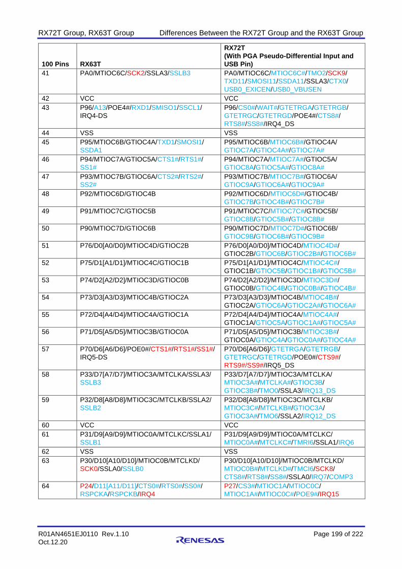
RX72T Group, RX63T Group Differences Between the RX72T Group and the RX63T Group
R01AN4651EJ0110 Rev.1.10 Page 199 of 222
Oct.12.20
100 Pins RX63T
RX72T
(With PGA Pseudo-Differential Input and
USB Pin)
41 PA0/MTIOC6C/SCK2/SSLA3/SSLB3 PA0/MTIOC6C/MTIOC6C#/TMO2/SCK9/
TXD11/SMOSI11/SSDA11/SSLA3/CTX0/
USB0_EXICEN/USB0_VBUSEN
42 VCC VCC
43 P96/A13/POE4#/RXD1/SMISO1/SSCL1/
IRQ4-DS
P96/CS0#/WAIT#/GTETRGA/GTETRGB/
GTETRGC/GTETRGD/POE4#/CTS8#/
RTS8#/SS8#/IRQ4_DS
44 VSS VSS
45 P95/MTIOC6B/GTIOC4A/TXD1/SMOSI1/
SSDA1
P95/MTIOC6B/MTIOC6B#/GTIOC4A/
GTIOC7A/GTIOC4A#/GTIOC7A#
46 P94/MTIOC7A/GTIOC5A/CTS1#/RTS1#/
SS1#
P94/MTIOC7A/MTIOC7A#/GTIOC5A/
GTIOC8A/GTIOC5A#/GTIOC8A#
47 P93/MTIOC7B/GTIOC6A/CTS2#/RTS2#/
SS2#
P93/MTIOC7B/MTIOC7B#/GTIOC6A/
GTIOC9A/GTIOC6A#/GTIOC9A#
48 P92/MTIOC6D/GTIOC4B P92/MTIOC6D/MTIOC6D#/GTIOC4B/
GTIOC7B/GTIOC4B#/GTIOC7B#
49 P91/MTIOC7C/GTIOC5B P91/MTIOC7C/MTIOC7C#/GTIOC5B/
GTIOC8B/GTIOC5B#/GTIOC8B#
50 P90/MTIOC7D/GTIOC6B P90/MTIOC7D/MTIOC7D#/GTIOC6B/
GTIOC9B/GTIOC6B#/GTIOC9B#
51 P76/D0[A0/D0]/MTIOC4D/GTIOC2B P76/D0[A0/D0]/MTIOC4D/MTIOC4D#/
GTIOC2B/GTIOC6B/GTIOC2B#/GTIOC6B#
52 P75/D1[A1/D1]/MTIOC4C/GTIOC1B P75/D1[A1/D1]/MTIOC4C/MTIOC4C#/
GTIOC1B/GTIOC5B/GTIOC1B#/GTIOC5B#
53 P74/D2[A2/D2]/MTIOC3D/GTIOC0B P74/D2[A2/D2]/MTIOC3D/MTIOC3D#/
GTIOC0B/GTIOC4B/GTIOC0B#/GTIOC4B#
54 P73/D3[A3/D3]/MTIOC4B/GTIOC2A P73/D3[A3/D3]/MTIOC4B/MTIOC4B#/
GTIOC2A/GTIOC6A/GTIOC2A#/GTIOC6A#
55 P72/D4[A4/D4]/MTIOC4A/GTIOC1A P72/D4[A4/D4]/MTIOC4A/MTIOC4A#/
GTIOC1A/GTIOC5A/GTIOC1A#/GTIOC5A#
56 P71/D5[A5/D5]/MTIOC3B/GTIOC0A P71/D5[A5/D5]/MTIOC3B/MTIOC3B#/
GTIOC0A/GTIOC4A/GTIOC0A#/GTIOC4A#
57 P70/D6[A6/D6]/POE0#/CTS1#/RTS1#/SS1#/
IRQ5-DS
P70/D6[A6/D6]/GTETRGA/GTETRGB/
GTETRGC/GTETRGD/POE0#/CTS9#/
RTS9#/SS9#/IRQ5_DS
58 P33/D7[A7/D7]/MTIOC3A/MTCLKA/SSLA3/
SSLB3
P33/D7[A7/D7]/MTIOC3A/MTCLKA/
MTIOC3A#/MTCLKA#/GTIOC3B/
GTIOC3B#/TMO0/SSLA3/IRQ13_DS
59 P32/D8[A8/D8]/MTIOC3C/MTCLKB/SSLA2/
SSLB2
P32/D8[A8/D8]/MTIOC3C/MTCLKB/
MTIOC3C#/MTCLKB#/GTIOC3A/
GTIOC3A#/TMO6/SSLA2/IRQ12_DS
60 VCC VCC
61 P31/D9[A9/D9]/MTIOC0A/MTCLKC/SSLA1/
SSLB1
P31/D9[A9/D9]/MTIOC0A/MTCLKC/
MTIOC0A#/MTCLKC#/TMRI6/SSLA1/IRQ6
62 VSS VSS
63 P30/D10[A10/D10]/MTIOC0B/MTCLKD/
SCK0/SSLA0/SSLB0
P30/D10[A10/D10]/MTIOC0B/MTCLKD/
MTIOC0B#/MTCLKD#/TMCI6/SCK8/
CTS8#/RTS8#/SS8#/SSLA0/IRQ7/COMP3
64 P24/D11[A11/D11]/CTS0#/RTS0#/SS0#/
RSPCKA/RSPCKB/IRQ4
P27/CS3#/MTIOC1A/MTIOC0C/
MTIOC1A#/MTIOC0C#/POE9#/IRQ15

RX72T Group, RX63T Group Differences Between the RX72T Group and the RX63T Group
R01AN4651EJ0110 Rev.1.10 Page 200 of 222
Oct.12.20
100 Pins RX63T
RX72T
(With PGA Pseudo-Differential Input and
USB Pin)
65 P23/D12[A12/D12]/CACREF/TXD0/SMOSI0/
SSDA0/MOSIA/MOSIB/CTX1
P24/D11[A11/D11]/MTIC5U/MTIC5U#/
TMCI2/TMO6/CTS8#/RTS8#/SS8#/SCK8/
RSPCKA/IRQ4/COMP0
66 P22/D13[A13/D13]/RXD0/SMISO0/SSCL0/
MISOA/MISOB/CRX1/ADTRG#
P23/D12[A12/D12]/MTIC5V/MTIC5V#/
TMO2/CACREF/TXD8/SMOSI8/SSDA8/
TXD12/SMOSI12/SSDA12/TXDX12/
SIOX12/MOSIA/CTX0/IRQ11/COMP1
67 P21/D14[A14/D14]/MTCLKA/IRQ6-DS/
ADTRG1#
P22/D13[A13/D13]/MTIC5W/MTCLKD/
MTIC5W#/MTCLKD#/MTIOC9B/TMRI2/
TMO4/RXD8/SMISO8/SSCL8/RXD12/
SMISO12/SSCL12/RXDX12/MISOA/CRX0/
IRQ10/ADTRG2#/COMP2
68 P20/D15[A15/D15]/MTCLKB/IRQ7-DS/
ADTRG0#
P21/D14[A14/D14]/MTIOC9A/MTCLKA/
MTIOC9A#/MTCLKA#/TMCI4/TXD8/
SMOSI8/SSDA8/TXD12/SMOSI12/
SSDA12/TXDX12/SIOX12/MOSIA/
IRQ6_DS/AN217/ADTRG1#/COMP5
69 P65/A0/BC0#/AN5 P20/D15[A15/D15]/MTIOC9C/MTCLKB/
MTIOC9C#/MTCLKB#/TMRI4/CTS8#/
RTS8#/SS8#/SCK8/RSPCKA/IRQ7_DS/
AN216/ADTRG0#/COMP4
70 P64/A1/AN4 P65/A12/IRQ9/AN211/CMPC53/DA1
71 AVCC P64/A13/IRQ8/AN210/CMPC33/DA0
72 VREF AVCC2
73 AVSS AVSS2
74 P63/A2/AN3 P63/A12/A14/IRQ7/AN209/CMPC23
75 P62/A3/AN2 P62/A13/A15/IRQ6/AN208/CMPC43
76 P61/A4/AN1 P61/A14/A16/IRQ5/AN207/CMPC13
77 P60/A5/AN0 P60/A15/A17/IRQ4/AN206/CMPC03
78 P55/AN11/DA1 P55/A16/A18/IRQ3/AN203/CMPC32
79 P54/AN10/DA0 P54/A17/A19/IRQ2/AN202/CMPC22
80 P53/A6/AN9 P53/A18/A20/IRQ1/AN201/CMPC12
81 P52/A7/AN8 P52/IRQ0/AN200/CMPC02
82 P51/AN7 P47/AN103
83 P50/AN6 P46/AN102/CMPC50/CMPC51
84 P47/AN103/CVREFH P45/AN101/CMPC40/CMPC41
85 P46/AN102 P44/AN100/CMPC30/CMPC31
86 P45/AN101 PH4/AN107/PGAVSS1
87 P44/AN100 P43/AN003
88 P43/AN003/CVREFL P42/AN002/CMPC20/CMPC21
89 P42/AN002 P41/AN001/CMPC10/CMPC11
90 P41/AN001 P40/AN000/CMPC00/CMPC01
91 P40/AN000 PH0/AN007/PGAVSS0
92 AVCC0 AVCC1
93 VREFH0 AVCC0
94 VREFL0 AVSS0
95 AVSS0 AVSS1
96 P82/WAIT#/MTIC5U/SCK12/IRQ3 P82/ALE/WAIT#/MTIC5U/MTIC5U#/
TMO4/SCK6/SCK12/IRQ3/COMP5

RX72T Group, RX63T Group Differences Between the RX72T Group and the RX63T Group
R01AN4651EJ0110 Rev.1.10 Page 201 of 222
Oct.12.20
100 Pins RX63T
RX72T
(With PGA Pseudo-Differential Input and
USB Pin)
97 P81/A8/MTIC5V/TXD12/SMOSI12/SSDA12/
TXDX12/SIOX12
P81/CS2#/MTIC5V/MTIC5V#/TMCI4/
TXD6/SMOSI6/SSDA6/TXD12/SMOSI12/
SSDA12/TXDX12/SIOX12/COMP4
98 P80/A9/MTIC5W/RXD12/SMISO12/SSCL12/
RXDX12/IRQ5
P80/CS1#/MTIC5W/MTIC5W#/TMRI4/
RXD6/SMISO6/SSCL6/RXD12/SMISO12/
SSCL12/RXDX12/IRQ5/COMP3
99 P11/ALE/MTCLKC/IRQ1-DS P11/RD#/MTIOC3A/MTCLKC/
MTIOC3A#/MTCLKC#/MTIOC9D/
GTIOC3B/GTETRGA/GTIOC3B#/
GTETRGC/TMO3/POE9#/IRQ1_DS
100 P10/MTCLKD/IRQ0-DS P10/MTIOC9B/MTCLKD/MTIOC9B#/
MTCLKD#/GTETRGB/GTETRGD/TMRI3/
POE12#/CTS6#/RTS6#/SS6#/IRQ0_DS

RX72T Group, RX63T Group Differences Between the RX72T Group and the RX63T Group
R01AN4651EJ0110 Rev.1.10 Page 202 of 222
Oct.12.20
3.3 100-Pin Package (RX72T: With PGA Pseudo-Differential Input and Without USB Pins)
Table 3.3 is a comparative listing of the pin functions of 100-pin package products (RX72T: with PGA pseudo-differential input and without USB pins).
Table 3.3 Comparative Listing of 100-Pin Package Pin Functions
(RX72T: With PGA Pseudo-Differential Input and Without USB Pins)
100 Pins RX63T
RX72T
(With PGA Pseudo-Differential Input and
Without USB Pin)
1 PE5/BCLK/IRQ0 PE5/BCLK/MTIOC9D/MTIOC9D#/GTIOC3A/
GTETRGB/GTIOC3A#/GTETRGD/SCK9/
CTS9#/RTS9#/SS9#/IRQ0/ADST0
2 EMLE EMLE
3 VSS VSS
4 P01/RD#/CTS0#/RTS0#/SS0# UB/P00/A11/MTIOC9A/MTIOC9A#/CACREF/
RXD9/SMISO9/SSCL9/RXD12/SMISO12/
SSCL12/RXDX12/IRQ2/ADST1/COMP0
5 VCL VCL
6 P00/CS1#/CACREF MD/FINED
7 MD/FINED P01/A10/MTIOC9C/MTIOC9C#/GTETRGA/
GTETRGB/GTETRGC/GTETRGD/POE12#/
TXD9/SMOSI9/SSDA9/TXD12/SMOSI12/
SSDA12/TXDX12/SIOX12/IRQ4/ADST2/
COMP1
8 PE4/A10/POE10#/MTCLKC/IRQ1 PE4/A9/MTCLKC/MTCLKC#/GTETRGA/
GTETRGB/GTETRGC/GTETRGD/POE10#/
SCK9/IRQ1
9 PE3/A11/POE11#/MTCLKD/IRQ2-DS PE3/A8/MTCLKD/MTCLKD#/GTETRGA/
GTETRGB/GTETRGC/GTETRGD/POE11#/
CTS9#/RTS9#/SS9#/IRQ2_DS
10 RES# RES#
11 XTAL XTAL/P37
12 VSS VSS
13 EXTAL EXTAL/P36
14 VCC VCC
15 PE2/POE10#/NMI PE2/POE10#/NMI
16 PE1/WR0#/WR#/CTS12#/RTS12#/SS12#/
SSLA3/SSLB3
PE1/WR0#/WR#/MTIOC9D/MTIOC9D#/
TMO5/CTS5#/RTS5#/SS5#/CTS12#/
RTS12#/SS12#/SSLA3/IRQ15
17 PE0/WR1#/BC1#/WAIT#/SSLA2/SSLB2/
CRX1/IRQ7
PE0/WR1#/BC1#/WAIT#/MTIOC9B/
MTIOC9B#/TMCI1/TMCI5/RXD5/SMISO5/
SSCL5/SSLA2/CRX0/IRQ7
18 TRST#/PD7/GTIOC0A/CTS0#/RTS0#/SS0#/
SSLA1/SSLB1/CTX1
TRST#/PD7/MTIOC9A/MTIOC9A#/
GTIOC0A/GTIOC3A/GTIOC0A#/
GTIOC3A#/TMRI1/TMRI5/TXD5/SMOSI5/
SSDA5/SSLA1/CTX0/IRQ8
19 TMS/PD6/GTIOC0B/SSLA0/SSLB0 TMS/PD6/MTIOC9C/MTIOC9C#/GTIOC0B/
GTIOC3B/GTIOC0B#/GTIOC3B#/TMO1/
CTS1#/RTS1#/SS1#/CTS11#/RTS11#/
SS11#/SSLA0/IRQ5/ADST0
20 TDI/PD5/GTIOC1A/RXD1/SMISO1/SSCL1/
IRQ6
TDI/PD5/GTIOC1A/GTETRGA/GTIOC1A#/
TMRI0/TMRI6/RXD1/SMISO1/SSCL1/
RXD11/SMISO11/SSCL11/IRQ6

RX72T Group, RX63T Group Differences Between the RX72T Group and the RX63T Group
R01AN4651EJ0110 Rev.1.10 Page 203 of 222
Oct.12.20
100 Pins RX63T
RX72T
(With PGA Pseudo-Differential Input and
Without USB Pin)
21 TCK/FINEC/PD4/GTIOC1B/SCK1 TCK/PD4/GTIOC1B/GTETRGB/
GTIOC1B#/TMCI0/TMCI6/SCK1/SCK11/
IRQ2
22 TDO/PD3/GTIOC2A/TXD1/SMOSI1/SSDA1 TDO/PD3/GTIOC2A/GTETRGC/GTIOC2A#/
TMO0/TXD1/SMOSI1/SSDA1/TXD11/
SMOSI11/SSDA11
23 PD2/CS2#/GTIOC2B/MOSIA/MOSIB TRCLK/PD2/A7/GTIOC2B/GTIOC0A/
GTIOC2B#/GTIOC0A#/TMCI1/TMO4/
SCK5/SCK8/MOSIA
24 PD1/CS0#/GTIOC3A/MISOA/MISOB TRDATA3/PD1/A6/GTIOC3A/GTIOC0B/
GTIOC3A#/GTIOC0B#/TMO2/RXD8/
SMISO8/SSCL8/MISOA
25 PD0/A12/GTIOC3B/RSPCKA/RSPCKB TRDATA2/PD0/A5/GTIOC3B/GTIOC1A/
GTIOC3B#/GTIOC1A#/TMO6/TXD8/
SMOSI8/SSDA8/RSPCKA
26 PB7/A19/SCK12 TRDATA1/PB7/A4/GTIOC1B/GTIOC1B#/
SCK5/SCK11/SCK12
27 PB6/A18/RXD12/SMISO12/SSCL12/
RXDX12/CRX1/IRQ2
TRDATA0/PB6/A3/GTIOC2A/GTIOC2A#/
RXD5/SMISO5/SSCL5/RXD11/SMISO11/
SSCL11/RXD12/SMISO12/SSCL12/
RXDX12/CRX0/IRQ2
28 PB5/A17/TXD12/SMOSI12/SSDA12/
TXDX12/SIOX12/CTX1
TRSYNC/PB5/A2/GTIOC2B/GTIOC2B#/
TXD5/SMOSI5/SSDA5/TXD11/SMOSI11/
SSDA11/TXD12/SMOSI12/SSDA12/
TXDX12/SIOX12/CTX0
29 PLLVCC VCC
30 PB4/A16/POE8#/GTETRG0/IRQ3-DS PB4/A1/GTETRGA/GTETRGB/GTETRGC/
GTETRGD/POE8#/CTS5#/RTS5#/SS5#/
SCK11/CTS11#/RTS11#/SS11#/IRQ3_DS
31 PLLVSS VSS
32 PB3/A15/MTIOC0A/CACREF/SCK0 PB3/A7/MTIOC0A/MTIOC0A#/CACREF/
SCK6/RSPCKA/IRQ9
33 PB2/MTIOC0B/TXD0/SMOSI0/SSDA0/SDA0 PB2/A6/MTIOC0B/MTIOC0B#/GTADSM0/
TMRI0/TXD6/SMOSI6/SSDA6/SDA/ADSM0
34 PB1/MTIOC0C/RXD0/SMISO0/SSCL0/
SCL0/IRQ4
PB1/A5/MTIOC0C/MTIOC0C#/GTADSM1/
TMCI0/RXD6/SMISO6/SSCL6/SCL/IRQ4/
ADSM1
35 PB0/A14/MTIOC0D/MOSIA/MOSIB PB0/A0/A4/BC0#/MTIOC0D/MTIOC0D#/
TMO0/TXD6/SMOSI6/SSDA6/CTS11#/
RTS11#/SS11#/MOSIA/IRQ8/ADTRG2#
36 PA5/MTIOC1A/RXD0/SMISO0/SSCL0/
MISOA/MISOB/ADTRG1#
PA5/A3/MTIOC1A/MTIOC1A#/TMCI3/
RXD6/SMISO6/SSCL6/RXD8/SMISO8/
SSCL8/MISOA/IRQ1/ADTRG1#
37 PA4/MTIOC1B/TXD0/SMOSI0/SSDA0/
RSPCKA/RSPCKB/ADTRG0#
PA4/A2/MTIOC1B/MTIOC1B#/TMCI7/
SCK6/TXD8/SMOSI8/SSDA8/RSPCKA/
ADTRG0#
38 PA3/MTIOC2A/SCK0/SSLA0/SSLB0 PA3/A1/MTIOC2A/MTIOC2A#/GTADSM0/
TMRI7/TXD9/SMOSI9/SSDA9/SCK8/SSLA0
39 PA2/MTIOC2B/RXD2/SMISO2/SSCL2/
SSLA1/SSLB1
PA2/A0/BC0#/MTIOC2B/MTIOC2B#/
GTADSM1/TMO7/CTS6#/RTS6#/SS6#/
RXD9/SMISO9/SSCL9/SCK11/SSLA1

RX72T Group, RX63T Group Differences Between the RX72T Group and the RX63T Group
R01AN4651EJ0110 Rev.1.10 Page 204 of 222
Oct.12.20
100 Pins RX63T
RX72T
(With PGA Pseudo-Differential Input and
Without USB Pin)
40 PA1/MTIOC6A/TXD2/SMOSI2/SSDA2/
SSLA2/SSLB2
PA1/MTIOC6A/MTIOC6A#/TMO4/TXD9/
SMOSI9/SSDA9/RXD11/SMISO11/SSCL11/
SSLA2/CRX0/IRQ14_DS/ADTRG0#
41 PA0/MTIOC6C/SCK2/SSLA3/SSLB3 PA0/MTIOC6C/MTIOC6C#/TMO2/SCK9/
TXD11/SMOSI11/SSDA11/SSLA3/CTX0
42 VCC VCC
43 P96/A13/POE4#/RXD1/SMISO1/SSCL1/
IRQ4-DS
P96/CS0#/WAIT#/GTETRGA/GTETRGB/
GTETRGC/GTETRGD/POE4#/CTS8#/
RTS8#/SS8#/IRQ4_DS
44 VSS VSS
45 P95/MTIOC6B/GTIOC4A/TXD1/SMOSI1/
SSDA1
P95/MTIOC6B/MTIOC6B#/GTIOC4A/
GTIOC7A/GTIOC4A#/GTIOC7A#
46 P94/MTIOC7A/GTIOC5A/CTS1#/RTS1#/
SS1#
P94/MTIOC7A/MTIOC7A#/GTIOC5A/
GTIOC8A/GTIOC5A#/GTIOC8A#
47 P93/MTIOC7B/GTIOC6A/CTS2#/RTS2#/
SS2#
P93/MTIOC7B/MTIOC7B#/GTIOC6A/
GTIOC9A/GTIOC6A#/GTIOC9A#
48 P92/MTIOC6D/GTIOC4B P92/MTIOC6D/MTIOC6D#/GTIOC4B/
GTIOC7B/GTIOC4B#/GTIOC7B#
49 P91/MTIOC7C/GTIOC5B P91/MTIOC7C/MTIOC7C#/GTIOC5B/
GTIOC8B/GTIOC5B#/GTIOC8B#
50 P90/MTIOC7D/GTIOC6B P90/MTIOC7D/MTIOC7D#/GTIOC6B/
GTIOC9B/GTIOC6B#/GTIOC9B#
51 P76/D0[A0/D0]/MTIOC4D/GTIOC2B P76/D0[A0/D0]/MTIOC4D/MTIOC4D#/
GTIOC2B/GTIOC6B/GTIOC2B#/GTIOC6B#
52 P75/D1[A1/D1]/MTIOC4C/GTIOC1B P75/D1[A1/D1]/MTIOC4C/MTIOC4C#/
GTIOC1B/GTIOC5B/GTIOC1B#/GTIOC5B#
53 P74/D2[A2/D2]/MTIOC3D/GTIOC0B P74/D2[A2/D2]/MTIOC3D/MTIOC3D#/
GTIOC0B/GTIOC4B/GTIOC0B#/GTIOC4B#
54 P73/D3[A3/D3]/MTIOC4B/GTIOC2A P73/D3[A3/D3]/MTIOC4B/MTIOC4B#/
GTIOC2A/GTIOC6A/GTIOC2A#/GTIOC6A#
55 P72/D4[A4/D4]/MTIOC4A/GTIOC1A P72/D4[A4/D4]/MTIOC4A/MTIOC4A#/
GTIOC1A/GTIOC5A/GTIOC1A#/GTIOC5A#
56 P71/D5[A5/D5]/MTIOC3B/GTIOC0A P71/D5[A5/D5]/MTIOC3B/MTIOC3B#/
GTIOC0A/GTIOC4A/GTIOC0A#/GTIOC4A#
57 P70/D6[A6/D6]/POE0#/CTS1#/RTS1#/SS1#/
IRQ5-DS
P70/D6[A6/D6]/GTETRGA/GTETRGB/
GTETRGC/GTETRGD/POE0#/CTS9#/
RTS9#/SS9#/IRQ5_DS
58 P33/D7[A7/D7]/MTIOC3A/MTCLKA/SSLA3/
SSLB3
P33/D7[A7/D7]/MTIOC3A/MTCLKA/
MTIOC3A#/MTCLKA#/GTIOC3B/
GTIOC3B#/TMO0/SSLA3/IRQ13_DS
59 P32/D8[A8/D8]/MTIOC3C/MTCLKB/SSLA2/
SSLB2
P32/D8[A8/D8]/MTIOC3C/MTCLKB/
MTIOC3C#/MTCLKB#/GTIOC3A/
GTIOC3A#/TMO6/SSLA2/IRQ12_DS
60 VCC VCC
61 P31/D9[A9/D9]/MTIOC0A/MTCLKC/SSLA1/
SSLB1
P31/D9[A9/D9]/MTIOC0A/MTCLKC/
MTIOC0A#/MTCLKC#/TMRI6/SSLA1/IRQ6
62 VSS VSS
63 P30/D10[A10/D10]/MTIOC0B/MTCLKD/
SCK0/SSLA0/SSLB0
P30/D10[A10/D10]/MTIOC0B/MTCLKD/
MTIOC0B#/MTCLKD#/TMCI6/SCK8/
CTS8#/RTS8#/SS8#/SSLA0/IRQ7/COMP3
64 P24/D11[A11/D11]/CTS0#/RTS0#/SS0#/
RSPCKA/RSPCKB/IRQ4
P27/CS3#/MTIOC1A/MTIOC0C/
MTIOC1A#/MTIOC0C#/POE9#/IRQ15

RX72T Group, RX63T Group Differences Between the RX72T Group and the RX63T Group
R01AN4651EJ0110 Rev.1.10 Page 205 of 222
Oct.12.20
100 Pins RX63T
RX72T
(With PGA Pseudo-Differential Input and
Without USB Pin)
65 P23/D12[A12/D12]/CACREF/TXD0/SMOSI0/
SSDA0/MOSIA/MOSIB/CTX1
P24/D11[A11/D11]/MTIC5U/MTIC5U#/
TMCI2/TMO6/CTS8#/RTS8#/SS8#/SCK8/
RSPCKA/IRQ4/COMP0
66 P22/D13[A13/D13]/RXD0/SMISO0/SSCL0/
MISOA/MISOB/CRX1/ADTRG#
P23/D12[A12/D12]/MTIC5V/MTIC5V#/
TMO2/CACREF/TXD8/SMOSI8/SSDA8/
TXD12/SMOSI12/SSDA12/TXDX12/
SIOX12/MOSIA/CTX0/IRQ11/COMP1
67 P21/D14[A14/D14]/MTCLKA/IRQ6-DS/
ADTRG1#
P22/D13[A13/D13]/MTIC5W/MTCLKD/
MTIC5W#/MTCLKD#/MTIOC9B/TMRI2/
TMO4/RXD8/SMISO8/SSCL8/RXD12/
SMISO12/SSCL12/RXDX12/MISOA/CRX0/
IRQ10/ADTRG2#/COMP2
68 P20/D15[A15/D15]/MTCLKB/IRQ7-DS/
ADTRG0#
P21/D14[A14/D14]/MTIOC9A/MTCLKA/
MTIOC9A#/MTCLKA#/TMCI4/TXD8/
SMOSI8/SSDA8/TXD12/SMOSI12/
SSDA12/TXDX12/SIOX12/MOSIA/
IRQ6_DS/AN217/ADTRG1#/COMP5
69 P65/A0/BC0#/AN5 P20/D15[A15/D15]/MTIOC9C/MTCLKB/
MTIOC9C#/MTCLKB#/TMRI4/CTS8#/
RTS8#/SS8#/SCK8/RSPCKA/IRQ7_DS/
AN216/ADTRG0#/COMP4
70 P64/A1/AN4 P65/A12/IRQ9/AN211/CMPC53/DA1
71 AVCC P64/A13/IRQ8/AN210/CMPC33/DA0
72 VREF AVCC2
73 AVSS AVSS2
74 P63/A2/AN3 P63/A12/A14/IRQ7/AN209/CMPC23
75 P62/A3/AN2 P62/A13/A15/IRQ6/AN208/CMPC43
76 P61/A4/AN1 P61/A14/A16/IRQ5/AN207/CMPC13
77 P60/A5/AN0 P60/A15/A17/IRQ4/AN206/CMPC03
78 P55/AN11/DA1 P55/A16/A18/IRQ3/AN203/CMPC32
79 P54/AN10/DA0 P54/A17/A19/IRQ2/AN202/CMPC22
80 P53/A6/AN9 P53/A18/A20/IRQ1/AN201/CMPC12
81 P52/A7/AN8 P52/IRQ0/AN200/CMPC02
82 P51/AN7 P47/AN103
83 P50/AN6 P46/AN102/CMPC50/CMPC51
84 P47/AN103/CVREFH P45/AN101/CMPC40/CMPC41
85 P46/AN102 P44/AN100/CMPC30/CMPC31
86 P45/AN101 PH4/AN107/PGAVSS1
87 P44/AN100 P43/AN003
88 P43/AN003/CVREFL P42/AN002/CMPC20/CMPC21
89 P42/AN002 P41/AN001/CMPC10/CMPC11
90 P41/AN001 P40/AN000/CMPC00/CMPC01
91 P40/AN000 PH0/AN007/PGAVSS0
92 AVCC0 AVCC1
93 VREFH0 AVCC0
94 VREFL0 AVSS0
95 AVSS0 AVSS1
96 P82/WAIT#/MTIC5U/SCK12/IRQ3 P82/ALE/WAIT#/MTIC5U/MTIC5U#/
TMO4/SCK6/SCK12/IRQ3/COMP5

RX72T Group, RX63T Group Differences Between the RX72T Group and the RX63T Group
R01AN4651EJ0110 Rev.1.10 Page 206 of 222
Oct.12.20
100 Pins RX63T
RX72T
(With PGA Pseudo-Differential Input and
Without USB Pin)
97 P81/A8/MTIC5V/TXD12/SMOSI12/SSDA12/
TXDX12/SIOX12
P81/CS2#/MTIC5V/MTIC5V#/TMCI4/
TXD6/SMOSI6/SSDA6/TXD12/SMOSI12/
SSDA12/TXDX12/SIOX12/COMP4
98 P80/A9/MTIC5W/RXD12/SMISO12/SSCL12/
RXDX12/IRQ5
P80/CS1#/MTIC5W/MTIC5W#/TMRI4/
RXD6/SMISO6/SSCL6/RXD12/SMISO12/
SSCL12/RXDX12/IRQ5/COMP3
99 P11/ALE/MTCLKC/IRQ1-DS P11/RD#/MTIOC3A/MTCLKC/
MTIOC3A#/MTCLKC#/MTIOC9D/
GTIOC3B/GTETRGA/GTIOC3B#/
GTETRGC/TMO3/POE9#/IRQ1_DS
100 P10/MTCLKD/IRQ0-DS P10/MTIOC9B/MTCLKD/MTIOC9B#/
MTCLKD#/GTETRGB/GTETRGD/TMRI3/
POE12#/CTS6#/RTS6#/SS6#/IRQ0_DS

RX72T Group, RX63T Group Differences Between the RX72T Group and the RX63T Group
R01AN4651EJ0110 Rev.1.10 Page 207 of 222
Oct.12.20
3.4 100-Pin Package (RX72T: Without PGA Pseudo-Differential Input and USB Pins)
Table 3.4 is a comparative listing of the pin functions of 100-pin package products (RX72T: without PGA pseudo-differential input and USB pins).
Table 3.4 Comparative Listing of 100-Pin Package Pin Functions
(RX72T: Without PGA Pseudo-Differential Input and USB Pins)
100 Pins RX63T
RX72T
(Without PGA Pseudo-Differential Input
and USB Pin)
1 PE5/BCLK/IRQ0 PE5/BCLK/MTIOC9D/MTIOC9D#/GTIOC3A/
GTETRGB/GTIOC3A#/GTETRGD/SCK9/
CTS9#/RTS9#/SS9#/IRQ0/ADST0
2 EMLE EMLE
3 VSS VSS
4 P01/RD#/CTS0#/RTS0#/SS0# UB/P00/A11/MTIOC9A/MTIOC9A#/CACREF/
RXD9/SMISO9/SSCL9/RXD12/SMISO12/
SSCL12/RXDX12/IRQ2/ADST1/COMP0
5 VCL VCL
6 P00/CS1#/CACREF MD/FINED
7 MD/FINED P01/A10/MTIOC9C/MTIOC9C#/GTETRGA/
GTETRGB/GTETRGC/GTETRGD/POE12#/
TXD9/SMOSI9/SSDA9/TXD12/SMOSI12/
SSDA12/TXDX12/SIOX12/IRQ4/ADST2/
COMP1
8 PE4/A10/POE10#/MTCLKC/IRQ1 PE4/A9/MTCLKC/MTCLKC#/GTETRGA/
GTETRGB/GTETRGC/GTETRGD/POE10#/
SCK9/IRQ1
9 PE3/A11/POE11#/MTCLKD/IRQ2-DS PE3/A8/MTCLKD/MTCLKD#/GTETRGA/
GTETRGB/GTETRGC/GTETRGD/POE11#/
CTS9#/RTS9#/SS9#/IRQ2_DS
10 RES# RES#
11 XTAL XTAL/P37
12 VSS VSS
13 EXTAL EXTAL/P36
14 VCC VCC
15 PE2/POE10#/NMI PE2/POE10#/NMI
16 PE1/WR0#/WR#/CTS12#/RTS12#/SS12#/
SSLA3/SSLB3
PE1/WR0#/WR#/MTIOC9D/MTIOC9D#/
TMO5/CTS5#/RTS5#/SS5#/CTS12#/
RTS12#/SS12#/SSLA3/IRQ15
17 PE0/WR1#/BC1#/WAIT#/SSLA2/SSLB2/
CRX1/IRQ7
PE0/WR1#/BC1#/WAIT#/MTIOC9B/
MTIOC9B#/TMCI1/TMCI5/RXD5/SMISO5/
SSCL5/SSLA2/CRX0/IRQ7
18 TRST#/PD7/GTIOC0A/CTS0#/RTS0#/SS0#/
SSLA1/SSLB1/CTX1
TRST#/PD7/MTIOC9A/MTIOC9A#/
GTIOC0A/GTIOC3A/GTIOC0A#/
GTIOC3A#/TMRI1/TMRI5/TXD5/SMOSI5/
SSDA5/SSLA1/CTX0/IRQ8
19 TMS/PD6/GTIOC0B/SSLA0/SSLB0 TMS/PD6/MTIOC9C/MTIOC9C#/GTIOC0B/
GTIOC3B/GTIOC0B#/GTIOC3B#/TMO1/
CTS1#/RTS1#/SS1#/CTS11#/RTS11#/
SS11#/SSLA0/IRQ5/ADST0
20 TDI/PD5/GTIOC1A/RXD1/SMISO1/SSCL1/
IRQ6
TDI/PD5/GTIOC1A/GTETRGA/GTIOC1A#/
TMRI0/TMRI6/RXD1/SMISO1/SSCL1/
RXD11/SMISO11/SSCL11/IRQ6

RX72T Group, RX63T Group Differences Between the RX72T Group and the RX63T Group
R01AN4651EJ0110 Rev.1.10 Page 208 of 222
Oct.12.20
100 Pins RX63T
RX72T
(Without PGA Pseudo-Differential Input
and USB Pin)
21 TCK/FINEC/PD4/GTIOC1B/SCK1 TCK/PD4/GTIOC1B/GTETRGB/GTIOC1B#/
TMCI0/TMCI6/SCK1/SCK11/IRQ2
22 TDO/PD3/GTIOC2A/TXD1/SMOSI1/SSDA1 TDO/PD3/GTIOC2A/GTETRGC/GTIOC2A#/
TMO0/TXD1/SMOSI1/SSDA1/TXD11/
SMOSI11/SSDA11
23 PD2/CS2#/GTIOC2B/MOSIA/MOSIB TRCLK/PD2/A7/GTIOC2B/GTIOC0A/
GTIOC2B#/GTIOC0A#/TMCI1/TMO4/
SCK5/SCK8/MOSIA
24 PD1/CS0#/GTIOC3A/MISOA/MISOB TRDATA3/PD1/A6/GTIOC3A/GTIOC0B/
GTIOC3A#/GTIOC0B#/TMO2/RXD8/
SMISO8/SSCL8/MISOA
25 PD0/A12/GTIOC3B/RSPCKA/RSPCKB TRDATA2/PD0/A5/GTIOC3B/GTIOC1A/
GTIOC3B#/GTIOC1A#/TMO6/TXD8/
SMOSI8/SSDA8/RSPCKA
26 PB7/A19/SCK12 TRDATA1/PB7/A4/GTIOC1B/GTIOC1B#/
SCK5/SCK11/SCK12
27 PB6/A18/RXD12/SMISO12/SSCL12/
RXDX12/CRX1/IRQ2
TRDATA0/PB6/A3/GTIOC2A/GTIOC2A#/
RXD5/SMISO5/SSCL5/RXD11/SMISO11/
SSCL11/RXD12/SMISO12/SSCL12/
RXDX12/CRX0/IRQ2
28 PB5/A17/TXD12/SMOSI12/SSDA12/
TXDX12/SIOX12/CTX1
TRSYNC/PB5/A2/GTIOC2B/GTIOC2B#/
TXD5/SMOSI5/SSDA5/TXD11/SMOSI11/
SSDA11/TXD12/SMOSI12/SSDA12/
TXDX12/SIOX12/CTX0
29 PLLVCC VCC
30 PB4/A16/POE8#/GTETRG0/IRQ3-DS PB4/A1/GTETRGA/GTETRGB/GTETRGC/
GTETRGD/POE8#/CTS5#/RTS5#/SS5#/
SCK11/CTS11#/RTS11#/SS11#/IRQ3_DS
31 PLLVSS VSS
32 PB3/A15/MTIOC0A/CACREF/SCK0 PB3/A7/MTIOC0A/MTIOC0A#/CACREF/
SCK6/ RSPCKA/IRQ9
33 PB2/MTIOC0B/TXD0/SMOSI0/SSDA0/SDA0 PB2/A6/MTIOC0B/MTIOC0B#/GTADSM0/
TMRI0/TXD6/SMOSI6/SSDA6/SDA/ADSM0
34 PB1/MTIOC0C/RXD0/SMISO0/SSCL0/SCL0/
IRQ4
PB1/A5/MTIOC0C/MTIOC0C#/GTADSM1/
TMCI0/RXD6/SMISO6/SSCL6/SCL/IRQ4/
ADSM1
35 PB0/A14/MTIOC0D/MOSIA/MOSIB PB0/A0/A4/BC0#/MTIOC0D/MTIOC0D#/
TMO0/TXD6/SMOSI6/SSDA6/CTS11#/
RTS11#/SS11#/MOSIA/IRQ8/ADTRG2#
36 PA5/MTIOC1A/RXD0/SMISO0/SSCL0/
MISOA/MISOB/ADTRG1#
PA5/A3/MTIOC1A/MTIOC1A#/TMCI3/
RXD6/SMISO6/SSCL6/RXD8/SMISO8/
SSCL8/MISOA/IRQ1/ADTRG1#
37 PA4/MTIOC1B/TXD0/SMOSI0/SSDA0/
RSPCKA/RSPCKB/ADTRG0#
PA4/A2/MTIOC1B/MTIOC1B#/TMCI7/
SCK6/TXD8/SMOSI8/SSDA8/RSPCKA/
ADTRG0#
38 PA3/MTIOC2A/SCK0/SSLA0/SSLB0 PA3/A1/MTIOC2A/MTIOC2A#/GTADSM0/
TMRI7/TXD9/SMOSI9/SSDA9/SCK8/SSLA0
39 PA2/MTIOC2B/RXD2/SMISO2/SSCL2/
SSLA1/SSLB1
PA2/A0/BC0#/MTIOC2B/MTIOC2B#/
GTADSM1/TMO7/CTS6#/RTS6#/SS6#/
RXD9/SMISO9/SSCL9/SCK11/SSLA1

RX72T Group, RX63T Group Differences Between the RX72T Group and the RX63T Group
R01AN4651EJ0110 Rev.1.10 Page 209 of 222
Oct.12.20
100 Pins RX63T
RX72T
(Without PGA Pseudo-Differential Input
and USB Pin)
40 PA1/MTIOC6A/TXD2/SMOSI2/SSDA2/
SSLA2/SSLB2
PA1/MTIOC6A/MTIOC6A#/TMO4/TXD9/
SMOSI9/SSDA9/RXD11/SMISO11/SSCL11/
SSLA2/CRX0/IRQ14_DS/ADTRG0#
41 PA0/MTIOC6C/SCK2/SSLA3/SSLB3 PA0/MTIOC6C/MTIOC6C#/TMO2/SCK9/
TXD11/SMOSI11/SSDA11/SSLA3/CTX0
42 VCC VCC
43 P96/A13/POE4#/RXD1/SMISO1/SSCL1/
IRQ4-DS
P96/CS0#/WAIT#/GTETRGA/
GTETRGB/GTETRGC/GTETRGD/
POE4#/CTS8#/RTS8#/SS8#/IRQ4_DS
44 VSS VSS
45 P95/MTIOC6B/GTIOC4A/TXD1/SMOSI1/
SSDA1
P95/MTIOC6B/MTIOC6B#/GTIOC4A/
GTIOC7A/GTIOC4A#/GTIOC7A#
46 P94/MTIOC7A/GTIOC5A/CTS1#/RTS1#/
SS1#
P94/MTIOC7A/MTIOC7A#/GTIOC5A/
GTIOC8A/GTIOC5A#/GTIOC8A#
47 P93/MTIOC7B/GTIOC6A/CTS2#/RTS2#/
SS2#
P93/MTIOC7B/MTIOC7B#/GTIOC6A/
GTIOC9A/GTIOC6A#/GTIOC9A#
48 P92/MTIOC6D/GTIOC4B P92/MTIOC6D/MTIOC6D#/GTIOC4B/
GTIOC7B/GTIOC4B#/GTIOC7B#
49 P91/MTIOC7C/GTIOC5B P91/MTIOC7C/MTIOC7C#/GTIOC5B/
GTIOC8B/GTIOC5B#/GTIOC8B#
50 P90/MTIOC7D/GTIOC6B P90/MTIOC7D/MTIOC7D#/GTIOC6B/
GTIOC9B/GTIOC6B#/GTIOC9B#
51 P76/D0[A0/D0]/MTIOC4D/GTIOC2B P76/D0[A0/D0]/MTIOC4D/MTIOC4D#/
GTIOC2B/GTIOC6B/GTIOC2B#/GTIOC6B#
52 P75/D1[A1/D1]/MTIOC4C/GTIOC1B P75/D1[A1/D1]/MTIOC4C/MTIOC4C#/
GTIOC1B/GTIOC5B/GTIOC1B#/GTIOC5B#
53 P74/D2[A2/D2]/MTIOC3D/GTIOC0B P74/D2[A2/D2]/MTIOC3D/MTIOC3D#/
GTIOC0B/GTIOC4B/GTIOC0B#/GTIOC4B#
54 P73/D3[A3/D3]/MTIOC4B/GTIOC2A P73/D3[A3/D3]/MTIOC4B/MTIOC4B#/
GTIOC2A/GTIOC6A/GTIOC2A#/GTIOC6A#
55 P72/D4[A4/D4]/MTIOC4A/GTIOC1A P72/D4[A4/D4]/MTIOC4A/MTIOC4A#/
GTIOC1A/GTIOC5A/GTIOC1A#/GTIOC5A#
56 P71/D5[A5/D5]/MTIOC3B/GTIOC0A P71/D5[A5/D5]/MTIOC3B/MTIOC3B#/
GTIOC0A/GTIOC4A/GTIOC0A#/GTIOC4A#
57 P70/D6[A6/D6]/POE0#/CTS1#/RTS1#/SS1#/
IRQ5-DS
P70/D6[A6/D6]/GTETRGA/GTETRGB/
GTETRGC/GTETRGD/POE0#/CTS9#/
RTS9#/SS9#/IRQ5_DS
58 P33/D7[A7/D7]/MTIOC3A/MTCLKA/SSLA3/
SSLB3
P33/D7[A7/D7]/MTIOC3A/MTCLKA/
MTIOC3A#/MTCLKA#/GTIOC3B/
GTIOC3B#/TMO0/SSLA3/IRQ13_DS
59 P32/D8[A8/D8]/MTIOC3C/MTCLKB/SSLA2/
SSLB2
P32/D8[A8/D8]/MTIOC3C/MTCLKB/
MTIOC3C#/MTCLKB#/GTIOC3A/
GTIOC3A#/TMO6/SSLA2/IRQ12_DS
60 VCC VCC
61 P31/D9[A9/D9]/MTIOC0A/MTCLKC/SSLA1/
SSLB1
P31/D9[A9/D9]/MTIOC0A/MTCLKC/
MTIOC0A#/MTCLKC#/TMRI6/SSLA1/IRQ6
62 VSS VSS
63 P30/D10[A10/D10]/MTIOC0B/MTCLKD/
SCK0/SSLA0/SSLB0
P30/D10[A10/D10]/MTIOC0B/MTCLKD/
MTIOC0B#/MTCLKD#/TMCI6/SCK8/
CTS8#/RTS8#/SS8#/SSLA0/IRQ7/COMP3

RX72T Group, RX63T Group Differences Between the RX72T Group and the RX63T Group
R01AN4651EJ0110 Rev.1.10 Page 210 of 222
Oct.12.20
100 Pins RX63T
RX72T
(Without PGA Pseudo-Differential Input
and USB Pin)
64 P24/D11[A11/D11]/CTS0#/RTS0#/SS0#/
RSPCKA/RSPCKB/IRQ4
P24/D11[A11/D11]/MTIC5U/MTIC5U#/
TMCI2/TMO6/CTS8#/RTS8#/SS8#/SCK8/
RSPCKA/IRQ4/COMP0
65 P23/D12[A12/D12]/CACREF/TXD0/SMOSI0/
SSDA0/MOSIA/MOSIB/CTX1
P23/D12[A12/D12]/MTIC5V/MTIC5V#/
TMO2/CACREF/TXD8/SMOSI8/SSDA8/
TXD12/SMOSI12/SSDA12/TXDX12/
SIOX12/MOSIA/CTX0/IRQ11/COMP1
66 P22/D13[A13/D13]/RXD0/SMISO0/SSCL0/
MISOA/MISOB/CRX1/ADTRG#
P22/D13[A13/D13]/MTIC5W/MTCLKD/
MTIC5W#/MTCLKD#/MTIOC9B/TMRI2/
TMO4/RXD8/SMISO8/SSCL8/RXD12/
SMISO12/SSCL12/RXDX12/MISOA/CRX0/
IRQ10/ADTRG2#/COMP2
67 P21/D14[A14/D14]/MTCLKA/IRQ6-DS/
ADTRG1#
P21/D14[A14/D14]/MTIOC9A/MTCLKA/
MTIOC9A#/MTCLKA#/TMCI4/TXD8/
SMOSI8/SSDA8/TXD12/SMOSI12/
SSDA12/TXDX12/SIOX12/MOSIA/
IRQ6_DS/AN217/ADTRG1#/COMP5
68 P20/D15[A15/D15]/MTCLKB/IRQ7-DS/
ADTRG0#
P20/D15[A15/D15]/MTIOC9C/MTCLKB/
MTIOC9C#/MTCLKB#/TMRI4/CTS8#/
RTS8#/SS8#/SCK8/RSPCKA/IRQ7_DS/
AN216/ADTRG0#/COMP4
69 P65/A0/BC0#/AN5 P65/A12/IRQ9/AN211/CMPC53/DA1
70 P64/A1/AN4 P64/A13/IRQ8/AN210/CMPC33/DA0
71 AVCC AVCC2
72 VREF AVCC2
73 AVSS AVSS2
74 P63/A2/AN3 P63/A12/A14/IRQ7/AN209/CMPC23
75 P62/A3/AN2 P62/A13/A15/IRQ6/AN208/CMPC43
76 P61/A4/AN1 P61/A14/A16/IRQ5/AN207/CMPC13
77 P60/A5/AN0 P60/A15/A17/IRQ4/AN206/CMPC03
78 P55/AN11/DA1 P55/A16/A18/IRQ3/AN203/CMPC32
79 P54/AN10/DA0 P54/A17/A19/IRQ2/AN202/CMPC22
80 P53/A6/AN9 P53/A18/A20/IRQ1/AN201/CMPC12
81 P52/A7/AN8 P52/IRQ0/AN200/CMPC02
82 P51/AN7 P51/AN205/CMPC52
83 P50/AN6 P50/AN204/CMPC42
84 P47/AN103/CVREFH P47/AN103
85 P46/AN102 P46/AN102/CMPC50/CMPC51
86 P45/AN101 P45/AN101/CMPC40/CMPC41
87 P44/AN100 P44/AN100/CMPC30/CMPC31
88 P43/AN003/CVREFL P43/AN003
89 P42/AN002 P42/AN002/CMPC20/CMPC21
90 P41/AN001 P41/AN001/CMPC10/CMPC11
91 P40/AN000 P40/AN000/CMPC00/CMPC01
92 AVCC0 AVCC1
93 VREFH0 AVCC0
94 VREFL0 AVSS0
95 AVSS0 AVSS1
96 P82/WAIT#/MTIC5U/SCK12/IRQ3 P82/ALE/WAIT#/MTIC5U/MTIC5U#/
TMO4/SCK6/SCK12/IRQ3/COMP5

RX72T Group, RX63T Group Differences Between the RX72T Group and the RX63T Group
R01AN4651EJ0110 Rev.1.10 Page 211 of 222
Oct.12.20
100 Pins RX63T
RX72T
(Without PGA Pseudo-Differential Input
and USB Pin)
97 P81/A8/MTIC5V/TXD12/SMOSI12/SSDA12/
TXDX12/SIOX12
P81/CS2#/MTIC5V/MTIC5V#/TMCI4/
TXD6/SMOSI6/SSDA6/TXD12/SMOSI12/
SSDA12/TXDX12/SIOX12/COMP4
98 P80/A9/MTIC5W/RXD12/SMISO12/SSCL12/
RXDX12/IRQ5
P80/CS1#/MTIC5W/MTIC5W#/TMRI4/
RXD6/SMISO6/SSCL6/RXD12/SMISO12/
SSCL12/RXDX12/IRQ5/COMP3
99 P11/ALE/MTCLKC/IRQ1-DS P11/RD#/MTIOC3A/MTCLKC/
MTIOC3A#/MTCLKC#/MTIOC9D/
GTIOC3B/GTETRGA/GTIOC3B#/
GTETRGC/TMO3/POE9#/IRQ1_DS
100 P10/MTCLKD/IRQ0-DS P10/MTIOC9B/MTCLKD/MTIOC9B#/
MTCLKD#/GTETRGB/GTETRGD/TMRI3/
POE12#/CTS6#/RTS6#/SS6#/IRQ0_DS

RX72T Group, RX63T Group Differences Between the RX72T Group and the RX63T Group
R01AN4651EJ0110 Rev.1.10 Page 212 of 222
Oct.12.20
4. Important Information when Migrating Between MCUs
This section presents important information on differences between the RX72T Group and the RX63T Group. 4.1, Notes on Pin Design, presents information regarding the hardware, and 4.2, Notes on Functional Design, presents information regarding the software.
4.1 Notes on Pin Design
Migration between the RX63T Group (100 pins) and the RX72T Group (100 pins: without PGA pseudo-differential input and USB) is simple because are largely pin-to-pin compatible with only a few suggestions. Note that some pins need to be handled differently between the two groups. Refer to Table 3.4, Comparative Listing of 100-Pin Package Pin Functions (RX72T: Without PGA Pseudo-Differential Input and USB Pins), for details.
4.1.1 VCL Pin (External Capacitor)
When using a smoothing capacitor connected to the VCL pin to stabilize the internal power supply, use a 0.1 μF capacitor for the RX63T Group and a 0.47 μF capacitor for the RX72T Group.
4.1.2 PLLVCC Pin
The RX72T Group does not have a PLLVCC pin.
4.1.3 Mode Setting Pins
On the RX63T Group the pins for setting the mode on release from the reset state are MD and P00, but on the RX72T Group they are MD and UB (multiplexed with P00).
4.1.4 Inputting an External Clock
When an external clock is input on the EXTAL pin, the counter-phase clock can be input on the XTAL pin on the RX63T Group, but the XTAL pin must be left open on the RX72T Group.
4.1.5 PGA Pseudo-Differential Input–Related Pins (P40 to P42, P44 to P46, PH0, and PH4)
On the RX72T Group a negative voltage may be input on the PGA pseudo-differential input pins from the reset state. Therefore, regardless of whether or not the PGA is used, it is necessary to change the settings of the PGA-related registers in order to use the pin functions of P40 to P42, P44 to P46, PH0, and PH4 after cancellation of a reset.
For details, refer to the descriptions of the VOLSR.PGAVLS bit, the initial setting sequence of the A/D converter, and the PIDR register in RX72T Group User’s Manual: Hardware.
Note that the above-mentioned setting changes are necessary even on products not equipped with PGA pseudo-differential inputs.
4.1.6 Inserting Decoupling Capacitors between AVCC and AVSS Pins
To prevent destruction of the RX72T Group’s analog input pins (AN000 to AN007, AN100 to AN107, AN200 to AN211, AN216, and AN217) by abnormal voltage such as an excessive surge, insert capacitors between AVCCn and AVSSn, and connect a protective circuit to protect the analog input pins (AN000 to AN007, AN100 to AN107, AN200 to AN211, AN216, and AN217).
For details, refer to the 12-Bit A/D Converter chapter in RX72T Group User’s Manual: Hardware.
4.1.7 Integrated USB DP/DM Pull-Up and Pull-Down Resistors
The RX72T Group is provided with integrated DP/DM pull-up and pull-down resistors. This means that it
uses a different USB external connection circuit configuration than the RX63T. For details, refer to 31.3.1.4,
Example of USB External Connection Circuit, in RX72T Group User’s Manual: Hardware.
RX72T Group, RX63T Group Differences Between the RX72T Group and the RX63T Group
R01AN4651EJ0110 Rev.1.10 Page 213 of 222
Oct.12.20
4.2 Notes on Functional Design
Some software that runs on the RX63T Group is compatible with the RX72T Group. However, careful evaluation is required since specifications such as operating timing and electrical characteristics differ between the groups.
This section presents notes on software regarding the settings of functions that differ between the RX72T Group and the RX63T Group.
For differences in modules and functions, refer to 2, Comparative Overview of Specifications. For further information, refer to the User’s Manual: Hardware listed in 5, Reference Documents.
4.2.1 Running RAM Self-Diagnostics on Save Register Banks
On the RX72T Group the save register banks are configured in the RAM. The save register banks are buffered, so writing to a bank with the SAVE instruction and then reading from the same bank with the RSTR instruction immediately afterwards may result in data being read from the buffer rather than from the RAM memory cells. When running RAM self-diagnostics on a save register bank, follow the steps below to ensure that the previously written data is read from the RAM rather than from the buffer.
(1) Use the SAVE instruction to write data to the bank on which self-diagnostics will be run.
(2) Use the SAVE instruction to write data to a bank other than that written to in step (1).
(3) Use the RSTR instruction to read data from the bank written to in step (1).
4.2.2 RIIC Operating Voltage Setting
When using the RIIC on the RX72T Group, it is necessary to specify the power supply voltage range in order to maintain the proper slope characteristics.
The initial setting is VCC = 4.5 V or greater. If a power supply voltage lower than 4.5 V will be used, change the voltage range setting before starting RIIC operation.
For details, refer to the description of the VOLSR.RICVLS bit in RX72T Group User’s Manual: Hardware.
4.2.3 USB Operating Voltage Setting
When using the USB module on the RX72T Group, it is necessary to set the UBS power supply control bit to 1 before starting USB operation.
For details, refer to the description of the VOLSR.USBVON bit in RX72T Group User’s Manual: Hardware.
4.2.4 Exception Vector Table
Addresses allocated in the vector table are fixed on the RX63T Group. On the RX72T Group, the vector table addresses are relocatable using the value set in the exception table register (EXTB) as the start address.
4.2.5 Voltage Level Setting
On the RX72T Group, values for the voltage level setting register (VOLSR) for operating modes, the voltage detection level select register (LVDLVLR) of the voltage detection circuit, and option function select register 1 (OFS1) for the option-setting memory need to be changed to appropriate values depending on the operating voltage. Make sure to set these values using a program.
4.2.6 Endian Setting
On the RX63T Group the endian setting is specified in the MDEB register (for user boot mode) or MDES register (single-chip mode) in the option-setting memory, but on the RX72T Group the endian setting is specified in the MDE register in the option-setting memory.
RX72T Group, RX63T Group Differences Between the RX72T Group and the RX63T Group
R01AN4651EJ0110 Rev.1.10 Page 214 of 222
Oct.12.20
4.2.7 Option-Setting Memory
ID codes used for ID code protection and ID code protection on connection of the on-chip debugger are located in the ROM on the RX63T Group and in the option-setting memory on the RX72T Group. Note that the setting procedures differ between the two groups.
4.2.8 Clock Frequency Settings
On the RX63T Group the clock frequency settings must be such that ICLK ≥ PCLK, but on the RX72T Group the settings must be as indicated below:
Requirements for clock frequency settings: ICLK ≥ BCLK, PCLKC ≥ PCLKA ≥ PCLKB
Requirements for clock frequency ratios: (N: integer)
ICLK:FCLK = N:1 or 1:N,
ICLK:PCLKA = N:1 or 1:N,
ICLK:PCLKB = N:1 or 1:N,
ICLK:PCLKC = N:1 or 1:N,
ICLK:PCLKD = N:1 or 1:N,
PCLKA:PCLKC = 1:1 or 1:2,
PCLKB:PCLKD = 1:1, 2:1, 4:1, or 1:2
Also, on the RX72T Group it is necessary to change the value of the MEMWAIT register when setting the frequency of ICLK to a frequency greater than 120 MHz.
4.2.9 PLL Circuit
On the RX63T Group the multiplication factor setting range of the PLL circuit is 8 to 50, but on the RX72T
Group it is 10 to 30 (in 0.5 increments). Change the setting to an appropriate value when using the PLL circuit. Also, on the RX72T Group use a program to switch the PLL clock.
4.2.10 MOSCWTCR Register
On the RX63T Group this register counts cycles of the main clock, but on the RX72T Group it counts cycles of the LOCO clock.
4.2.11 Operation of Main Clock Oscillation Stop Detection Function
The oscillation stop detection function detects when the operation of the main clock oscillator stops and supplies a LOCO clock using the output of the low-speed on-chip oscillator as the clock source for the system clock, instead of the main clock or PLL clock.
Note that on the RX72T Group, when the HOCO clock is selected as the PLL clock source and the PLL clock is selected as the system clock source, the system clock does not switch to the LOCO clock even if main clock oscillation stop is detected.
4.2.12 All-Module Clock Stop Mode
On the RX63T Group, 1 must be written to MSTPA27 and MSTPA29 when a transition is made to all-module clock stop mode.
On the RX72T Group, 1 must be written to MSTPA24, MSTPA27, MSTPA29, and MSTPD0 to MSTPD7 when a transition is made to all-module clock stop mode.
RX72T Group, RX63T Group Differences Between the RX72T Group and the RX63T Group
R01AN4651EJ0110 Rev.1.10 Page 215 of 222
Oct.12.20
4.2.13 Input Buffer Control by DIRQnE Bits (n = 0 to 15)
On the RX72T Group, setting the DPSIERy.DIRQnE (y = 0 or 1, n = 0 to 15) bit to 1 enables the input buffer of the corresponding pin among IRQ0-DS to IRQ15-DS. Note that once the input buffer is enabled, inputs on these pins are sent to the corresponding DPSIFRy.DIRQnF (y = 0 or 1, n = 0 to 15) bits, but they are not sent to the interrupt controller, peripheral modules, and I/O ports.
4.2.14 Software Configurable Interrupts
On the RX63T Group the interrupt sources have fixed vector numbers, but on the RX72T Group the MTU and GPTW interrupt sources are classified as software configurable interrupt A and set in software configurable interrupt A source select register n (SLIARn). This allows interrupt sources to be allocated to 208 to 255 in the interrupt vector table.
4.2.15 Initialization of Port Direction Register (PDR)
The method of initializing the PDR differs between the RX63T Group and RX72T Group, even on products with the same pin count.
4.2.16 Note on Controlling Switching to General I/O Port Pin Operation by POE3
On the RX72T Group, when an output disable request is generated by making a setting in POE3, pins for which the setting is 1 in the corresponding PMMCRn register (n = 0 to 3) of the POE3 are switched to general I/O port pin operation. Therefore, set the bits in the corresponding POECRn register (n = 0 to 3) to 0 beforehand.
4.2.17 Operating Frequencies of the GPTW and MTU3d
On the RX72T Group, the count clock for the GPTW and MTU3d is PCLKC, and the bus clock is PCLKA. Note that restrictions apply to the combinations of frequencies that may be used.
4.2.18 DMAC Activation by the MTU
On the RX72T Group, if the DMAC is activated by the MTU, the activation source is cleared when the DMAC requests ownership of the internal bus. Accordingly, the state of the internal bus may lead to a wait before the DMA transfer starts, even though the activation source has been cleared.
4.2.19 MTIOC Pin Output Level when Counter Stopped
When operating with the MTIOC pin in the output state, clearing the CSTn bit to 0 causes the counter to stop. When this happens in complementary PWM mode or reset synchronous PWM mode on the RX72T Group, the initial output level set in the TOCR1A or TOCR2A register is output on the MTIOC pin.
When operating in other than complementary PWM mode or reset synchronous PWM mode, the output compare output level of the MTIOC is maintained.
When a write to the TIOR register occurs while the value of the CSTn bit is 0, the output level of the pin is updated to the initial output value setting.
4.2.20 Note on Timer Mode Register Setting for ELC Event Input
When using the MTU for ELC operation on the RX72T Group, set the timer mode register (TMDR) of the relevant channel to its initial value (00h).
4.2.21 Port Output Enable
The port output enable registers on the RX72T Group are quite different from those on the RX63T Group. Note that software compatibility is low with regard to this function.

RX72T Group, RX63T Group Differences Between the RX72T Group and the RX63T Group
R01AN4651EJ0110 Rev.1.10 Page 216 of 222
Oct.12.20
4.2.22 Control in Response to Output Disabling Request on Port Output Enable 3
When a request to disable outputs is generated on the RX72T Group, pins for which the corresponding bits in the POECR1 to POECR3 and POECR7 registers are set to 1 enter the high-impedance state, and pins for which the corresponding bits in the PMMCR0 to PMMCR3 registers are set to 1 are switched to general I/O port pin operation.
When both bits are set to 1 for the same pin, the settings of the POECR1 to POECR3 and POECR7 registers take priority, and the pins enter the high-impedance state.
After a pin is switched to general I/O port pin operation, the settings of the corresponding bits in the PDR and PODR registers determine the state of the pin.
4.2.23 Setting the Active Level with MTU or GPTW Set to Inverted Output
On the RX72T Group the MPC.PmnPFS register can be used to specify normal output or inverted output for the MTU and GPTW.
When inverted output is selected on the MTU, the active level specified by the MTU.TOCR1j and MTU.TOCR2j registers (j = A, B) and the active level of the signals which are output to the pins is inverted. To use detection of simultaneous conduction in this case, specify in the ALR1 and ALR2 registers the active level based on the signals which are output to the pins.
When inverted output is selected on the GPTW, the active level of the signals which are output to the pins is inverted. To use detection of simultaneous conduction in this case, specify in the ALR3 to ALR5 registers the active level based on the signals which are output to the pins.
4.2.24 Reading Pins in High-Impedance State
When pins are put into the high-impedance state by the POE on the RX72T Group, their level cannot be read. The value when read is undefined. To read the level of the pins, release them from the high-impedance state.
This limitation does not apply when port switching control is selected instead of high-impedance control.
4.2.25 Note on Using POE and POEG Together
When using the POE and POEG together on the RX72T Group, do not apply output disable control by both the POE and POEG to the same GPTW output pin.
4.2.26 General PWM Timer
Registers for the general PWM timer on the RX72T Group are quite different from those on the RX63T Group. Note that software compatibility is low with regard to this function.
4.2.27 Watchdog Timer and Independent Watchdog Timer
On the RX72T Group it is possible to select either maskable or non-maskable as the type of the WDT underflow and refresh error interrupts and the IWDT underflow and refresh error interrupts.
4.2.28 Eliminating I2C Bus Interface Noise
The RX63T Group has integrated analog noise filters on the SCL and SDA lines, but the RX72T Group has no integrated analog noise filters.
4.2.29 12-Bit A/D Converter
Registers for the 12-bit A/D converter on the RX72T Group are quite different from those on the RX63T Group. Note that software compatibility is low with regard to this function.

RX72T Group, RX63T Group Differences Between the RX72T Group and the RX63T Group
R01AN4651EJ0110 Rev.1.10 Page 217 of 222
Oct.12.20
4.2.30 A/D Conversion Start Bit
On the RX72T Group, when the single-scan continuous function is used (ADGSPCR.GBRP bit = 1) with group priority control operation mode enabled on the 12-bit A/D converter (ADCSR.ADCS[1:0] bits = 01b and ADGSPCR.PGS bit = 1), the value of the ADCSR.ADST bit is maintained as 1.
4.2.31 Restrictions on Comparison Function
On the RX72T Group the comparison function of the 12-bit A/D converter has the following restrictions:
1. Use of self-diagnostics and double trigger mode are prohibited. (ADRD, ADDBLDR, ADDBLDRA, and
ADDBLDRB are not covered by the comparison function)
2. To use matching or unmatching output, it is necessary to select single scan mode.
3. When temperature sensor or internal reference voltage is selected for window A, operation of window B is
prohibited.
4. When temperature sensor or internal reference voltage is selected for window B, operation of window A is
prohibited.
5. The same channel cannot be set for both window A and window B.
6. It is necessary to make settings such that high-side reference value ≥ low-side reference value.
4.2.32 Generation of A/D Scan Conversion End Interrupt
On the RX72T Group, when scanning was started by a software trigger, an A/D scan conversion end interrupt is generated if the ADCSR.ADIE bit is set to 1 when the scan ends, even when double-trigger mode has been selected.
4.2.33 Scan Conversion Time of 12-Bit A/D Converter
The scan conversion times differ on the RX63T Group and RX72T Group. The scan conversion time (tSCAN), for a single scan where the number of selected channels is n, is shown below for each group. For details, refer to the descriptions of the 12-bit A/D converter analog input sampling time and scan conversion time in RX63T Group User’s Manual: Hardware and RX72T Group User’s Manual: Hardware.
RX63T: tSCAN = tD + tSPLSH + tDIAG + (tCONV n) + tED
RX72T: tSCAN = tD + tSPLSH + (tDIS n) + tDIAG + (tCONV n) + tED
tD: Start-of-scanning-delay time
tSPLSH: Channel-dedicated sample-and-hold circuit processing time
tDIS: Disconnection detection assistance processing time
tDIAG: Self-diagnostic A/D conversion processing time
tCONV: A/D conversion processing time
tED: End-of-scanning-delay time
4.2.34 D/A Converter Settings
When making D/A converter settings on the RX72T Group, first set comparator C as the output destination using the D/A destination select register (DADSELR), then wait for the D/A converter output to stabilize before enabling comparator operation.
Similarly, stop the comparator temporarily before making changes to the settings of the D/A converter, then wait for the D/A converter output to stabilize before enabling comparator operation.
4.2.35 ROM Cache
The RX72T Group has an 8 KB ROM cache, and ROM cache operation is disabled after a reset is canceled.
To use the ROM cache, set the ROMCE.ROMCEN bit to 1.

RX72T Group, RX63T Group Differences Between the RX72T Group and the RX63T Group
R01AN4651EJ0110 Rev.1.10 Page 218 of 222
Oct.12.20
4.2.36 Using Flash Memory Programming Commands
On the RX63T Group, programming and erasing the flash memory are performed by issuing commands to the FCU. On the RX72T Group, programming and erasing the flash memory are performed by controlling the FCU with the FACI commands specified in the FACI command issuing area.
Table 4.1 is a comparative listing of FCU and FACI commands.
Table 4.1 Comparison of Specifications Between FCU and FACI Commands
Item FCU Command (RX63T) FACI Command (RX72T)
Command issuing area P/E address
(00F8 0000h to 00FF FFFFh)
FACI command issuing area
(007E 0000h)
Available command • P/E normal mode transition
• Status read mode transition
• Lock bit read mode transition (lock
bit read 1)
• Peripheral clock notification
• Programming
• Block erase
• P/E suspend
• P/E resume
• Status register clear
• Lock bit read 2/blank check
• Lock bit programming
• Programming
• Block erase
• P/E suspend
• P/E resume
• Status clear
• Forced stop
• Lock-bit read
• Blank check
• Configuration setting
• Lock-bit programming
RX72T Group, RX63T Group Differences Between the RX72T Group and the RX63T Group
R01AN4651EJ0110 Rev.1.10 Page 219 of 222
Oct.12.20
5. Reference Documents
User’s Manual: Hardware
RX63T Group User’s Manual: Hardware, Rev. 2.20 (R01UH0238EJ0220)
(The latest version can be downloaded from the Renesas Electronics website.)
RX72T Group User’s Manual: Hardware, Rev. 1.00 (R01UH0803EJ0100)
(The latest version can be downloaded from the Renesas Electronics website.) Application Note
Design Guide for Migration between RX Family: Differences in Package External form (R01AN4591EJ)
(The latest version can be downloaded from the Renesas Electronics website.)
Technical Updates/Technical News
(The latest version can be downloaded from the Renesas Electronics website.)

RX72T Group, RX63T Group Differences Between the RX72T Group and the RX63T Group
R01AN4651EJ0110 Rev.1.10 Page 220 of 222
Oct.12.20
Related Technical Updates
This application note reflects the content of the following technical updates:
• TN-RX*-A151A/E
• TN-RX*-A152A/E
• TN-RX*-A161A/E
• TN-RX*-A186A/E
• TN-RX*-A193A/E
• TN-RX*-A0219A/E
• TN-RX*-A0226A/E
• TN-RX*-A0227A/E

RX72T Group, RX63T Group Differences Between the RX72T Group and the RX63T Group
R01AN4651EJ0110 Rev.1.10 Page 221 of 222
Oct.12.20
Revision History
Rev. Date
Description
Page Summary
1.00 Apr. 5, 2019 ⎯ First edition issued
1.10 Oct. 12, 2020 5 1 Table 1.1 Comparison of Built-In Functions of RX72T Group
and RX63T Group revised
8 2.1 Table 2.2 Comparison of CPU Registers revised
9 2.2 Table 2.3 Comparative Overview of Operating Modes
revised
10 2.3 Address Space added
13 2.4 Figure 2.4 Comparison of Option-Setting Memory Areas
added
39 2.10 Exception Handling added
42 2.11 Table 2.22 Comparison of Interrupt Controller Registers
revised
53 2.16 Table 2.32 Comparative Overview of I/O Ports on 100-
Pin Packages (RX72T: With PGA Pseudo-Differential Input)
revised
54 2.16 Table 2.33 Comparative Overview of I/O Ports on 100-
Pin Packages (RX72T: Without PGA Pseudo-Differential
Input) revised
2.16 Table 2.34 Comparison of I/O Port Functions added
56 2.16 Table 2.35 Comparison of I/O Port Registers revised
58 2.17 Table 2.36 Comparison of Multiplexed Pin Assignments
added
77 to 98 2.17 Table 2.39 to Table 2.55 Comparison of Pmn Pin
Function Control Register (PmnPFS) added
99 2.17 Table 2.56 Comparison of Multi-Function Pin Controller
Registers revised
103 2.18 Table 2.58 Comparison of Multi-Function Timer Pulse
Unit 3 Registers revised
105 2.18 Table 2.59 Comparison of TPSC Bit Settings (Other
Than MTU5) added
107 2.18 Table 2.60 Comparison of TPSC Bit Settings (MTU5)
added
111 2.19 Table 2.62 Comparison of Port Output Enable 3
Registers revised
128 2.20 Table 2.64 Comparison of General PWM Timer
Registers revised
136 2.20 Table 2.65 Comparative Listing of GTIOA and GTIOB Bit
Settings added
149 2.25 Table 2.75 Comparison of Serial Communications
Interface Registers revised
163 2.29 Table 2.82 Comparison of CRC Calculator Registers
revised
164 2.30 Table 2.83 Comparative Overview of 12-Bit A/D
Converters revised
171 2.30 Table 2.84 Comparison of 12-Bit A/D Converter
Registers revised
175 2.30 Table 2.85 Comparison of A/D Conversion Start Triggers
Set in ADSTRGR Register (144-, 120-, 112-, and 100-Pin
Versions) added
177 2.30 Table 2.86 Comparison of A/D Conversion Start Triggers
Set in ADSTRGR Register (64- and 48-Pin Versions)

RX72T Group, RX63T Group Differences Between the RX72T Group and the RX63T Group
R01AN4651EJ0110 Rev.1.10 Page 222 of 222
Oct.12.20
Rev. Date
Description
Page Summary
1.10 Oct. 12, 2020 181 2.33 Table 2.90 Comparative Overview of RAM revised
182 2.33 Table 2.91 Comparison of RAM Registers revised
183 2.34 Table 2.92 Comparative Overview of Flash Memory
revised
186 2.34 Table 2.93 Comparison of Flash Memory Registers
revised
197 3.2 Table 3.2 Comparative Listing of 100-Pin Package Pin
Functions (RX72T: With PGA Pseudo-Differential Input and
USB Pins) revised
202 3.3 Table 3.3 Comparative Listing of 100-Pin Package Pin
Functions (RX72T: With PGA Pseudo-Differential Input and
Without USB Pins) revised
207 3.4 Table 3.4 Comparative Listing of 100-Pin Package Pin
Functions (RX72T: Without PGA Pseudo-Differential Input
and USB Pins) revised
212 4.1.4 General I/O Ports deleted
4.1.7 Integrated USB DP/DM Pull-Up and Pull-Down
Resistors and 4.1.7 Inserting Decoupling Capacitors between
AVCC and AVSS Pins added
213 4.2.1 Running RAM Self-Diagnostics on Save Register Banks
added
214 4.2.10 MOSCWTCR Register added
214, 215 4.2.11, 4.2.13, 4.2.15, and 4.2.16 added
215, 216 4.2.19 and 4.2.22 to 4.2.24 added
216, 217 4.2.25, 4.2.27, 4.2.28, and 4.2.30 to 4.2.32 added
217 4.2.33 and 4.2.34 added
218 4.2.36 Table 4.1 Comparison of Specifications Between FCU
and FACI commands revised
219 5. Reference Documents revised
220 Related Technical Updates revised

General Precautions in the Handling of Microprocessing Unit and Microcontroller Unit Products
The following usage notes are applicable to all Microprocessing unit and Microcontroller unit products from Renesas. For detailed usage notes on the products covered by this document, refer to the relevant sections of the document as well as any technical updates that have been issued for the products.
1. Precaution against Electrostatic Discharge (ESD)
A strong electrical field, when exposed to a CMOS device, can cause destruction of the gate oxide and ultimately degrade the device operation. Steps
must be taken to stop the generation of static electricity as much as possible, and quickly dissipate it when it occurs. Environmental control must be
adequate. When it is dry, a humidifier should be used. This is recommended to avoid using insulators that can easily build up static electricity.
Semiconductor devices must be stored and transported in an anti-static container, static shielding bag or conductive material. All test and
measurement tools including work benches and floors must be grounded. The operator must also be grounded using a wrist strap. Semiconductor
devices must not be touched with bare hands. Similar precautions must be taken for printed circuit boards with mounted semiconductor devices.
2. Processing at power-on
The state of the product is undefined at the time when power is supplied. The states of internal circuits in the LSI are indeterminate and the states of
register settings and pins are undefined at the time when power is supplied. In a finished product where the reset signal is applied to the external reset
pin, the states of pins are not guaranteed from the time when power is supplied until the reset process is completed. In a similar way, the states of pins
in a product that is reset by an on-chip power-on reset function are not guaranteed from the time when power is supplied until the power reaches the
level at which resetting is specified.
3. Input of signal during power-off state
Do not input signals or an I/O pull-up power supply while the device is powered off. The current injection that results from input of such a signal or I/O
pull-up power supply may cause malfunction and the abnormal current that passes in the device at this time may cause degradation of internal
elements. Follow the guideline for input signal during power-off state as described in your product documentation.
4. Handling of unused pins
Handle unused pins in accordance with the directions given under handling of unused pins in the manual. The input pins of CMOS products are
generally in the high-impedance state. In operation with an unused pin in the open-circuit state, extra electromagnetic noise is induced in the vicinity of
the LSI, an associated shoot-through current flows internally, and malfunctions occur due to the false recognition of the pin state as an input signal
become possible.
5. Clock signals
After applying a reset, only release the reset line after the operating clock signal becomes stable. When switching the clock signal during program
execution, wait until the target clock signal is stabilized. When the clock signal is generated with an external resonator or from an external oscillator
during a reset, ensure that the reset line is only released after full stabilization of the clock signal. Additionally, when switching to a clock signal
produced with an external resonator or by an external oscillator while program execution is in progress, wait until the target clock signal is stable.
6. Voltage application waveform at input pin
Waveform distortion due to input noise or a reflected wave may cause malfunction. If the input of the CMOS device stays in the area between VIL
(Max.) and VIH (Min.) due to noise, for example, the device may malfunction. Take care to prevent chattering noise from entering the device when the
input level is fixed, and also in the transition period when the input level passes through the area between VIL (Max.) and VIH (Min.).
7. Prohibition of access to reserved addresses
Access to reserved addresses is prohibited. The reserved addresses are provided for possible future expansion of functions. Do not access these
addresses as the correct operation of the LSI is not guaranteed.
8. Differences between products
Before changing from one product to another, for example to a product with a different part number, confirm that the change will not lead to problems.
The characteristics of a microprocessing unit or microcontroller unit products in the same group but having a different part number might differ in terms
of internal memory capacity, layout pattern, and other factors, which can affect the ranges of electrical characteristics, such as characteristic values,
operating margins, immunity to noise, and amount of radiated noise. When changing to a product with a different part number, implement a system-
evaluation test for the given product.

© 2020 Renesas Electronics Corporation. All rights reserved.
Notice
1. Descriptions of circuits, software and other related information in this document are provided only to illustrate the operation of semiconductor products
and application examples. You are fully responsible for the incorporation or any other use of the circuits, software, and information in the design of your
product or system. Renesas Electronics disclaims any and all liability for any losses and damages incurred by you or third parties arising from the use
of these circuits, software, or information.
2. Renesas Electronics hereby expressly disclaims any warranties against and liability for infringement or any other claims involving patents, copyrights,
or other intellectual property rights of third parties, by or arising from the use of Renesas Electronics products or technical information described in this
document, including but not limited to, the product data, drawings, charts, programs, algorithms, and application examples.
3. No license, express, implied or otherwise, is granted hereby under any patents, copyrights or other intellectual property rights of Renesas Electronics
or others.
4. You shall not alter, modify, copy, or reverse engineer any Renesas Electronics product, whether in whole or in part. Renesas Electronics disclaims any
and all liability for any losses or damages incurred by you or third parties arising from such alteration, modification, copying or reverse engineering.
5. Renesas Electronics products are classified according to the following two quality grades: “Standard” and “High Quality”. The intended applications for
each Renesas Electronics product depends on the product’s quality grade, as indicated below.
"Standard": Computers; office equipment; communications equipment; test and measurement equipment; audio and visual equipment; home
electronic appliances; machine tools; personal electronic equipment; industrial robots; etc.
"High Quality": Transportation equipment (automobiles, trains, ships, etc.); traffic control (traffic lights); large-scale communication equipment; key
financial terminal systems; safety control equipment; etc.
Unless expressly designated as a high reliability product or a product for harsh environments in a Renesas Electronics data sheet or other Renesas
Electronics document, Renesas Electronics products are not intended or authorized for use in products or systems that may pose a direct threat to
human life or bodily injury (artificial life support devices or systems; surgical implantations; etc.), or may cause serious property damage (space
system; undersea repeaters; nuclear power control systems; aircraft control systems; key plant systems; military equipment; etc.). Renesas Electronics
disclaims any and all liability for any damages or losses incurred by you or any third parties arising from the use of any Renesas Electronics product
that is inconsistent with any Renesas Electronics data sheet, user’s manual or other Renesas Electronics document.
6. When using Renesas Electronics products, refer to the latest product information (data sheets, user’s manuals, application notes, “General Notes for
Handling and Using Semiconductor Devices” in the reliability handbook, etc.), and ensure that usage conditions are within the ranges specified by
Renesas Electronics with respect to maximum ratings, operating power supply voltage range, heat dissipation characteristics, installation, etc. Renesas
Electronics disclaims any and all liability for any malfunctions, failure or accident arising out of the use of Renesas Electronics products outside of such
specified ranges.
7. Although Renesas Electronics endeavors to improve the quality and reliability of Renesas Electronics products, semiconductor products have specific
characteristics, such as the occurrence of failure at a certain rate and malfunctions under certain use conditions. Unless designated as a high reliability
product or a product for harsh environments in a Renesas Electronics data sheet or other Renesas Electronics document, Renesas Electronics
products are not subject to radiation resistance design. You are responsible for implementing safety measures to guard against the possibility of bodily
injury, injury or damage caused by fire, and/or danger to the public in the event of a failure or malfunction of Renesas Electronics products, such as
safety design for hardware and software, including but not limited to redundancy, fire control and malfunction prevention, appropriate treatment for
aging degradation or any other appropriate measures. Because the evaluation of microcomputer software alone is very difficult and impractical, you are
responsible for evaluating the safety of the final products or systems manufactured by you.
8. Please contact a Renesas Electronics sales office for details as to environmental matters such as the environmental compatibility of each Renesas
Electronics product. You are responsible for carefully and sufficiently investigating applicable laws and regulations that regulate the inclusion or use of
controlled substances, including without limitation, the EU RoHS Directive, and using Renesas Electronics products in compliance with all these
applicable laws and regulations. Renesas Electronics disclaims any and all liability for damages or losses occurring as a result of your noncompliance
with applicable laws and regulations.
9. Renesas Electronics products and technologies shall not be used for or incorporated into any products or systems whose manufacture, use, or sale is
prohibited under any applicable domestic or foreign laws or regulations. You shall comply with any applicable export control laws and regulations
promulgated and administered by the governments of any countries asserting jurisdiction over the parties or transactions.
10. It is the responsibility of the buyer or distributor of Renesas Electronics products, or any other party who distributes, disposes of, or otherwise sells or
transfers the product to a third party, to notify such third party in advance of the contents and conditions set forth in this document.
11. This document shall not be reprinted, reproduced or duplicated in any form, in whole or in part, without prior written consent of Renesas Electronics.
12. Please contact a Renesas Electronics sales office if you have any questions regarding the information contained in this document or Renesas
Electronics products.
(Note1) “Renesas Electronics” as used in this document means Renesas Electronics Corporation and also includes its directly or indirectly controlled
subsidiaries.
(Note2) “Renesas Electronics product(s)” means any product developed or manufactured by or for Renesas Electronics.
(Rev.4.0-1 November 2017)
Corporate Headquarters Contact information TOYOSU FORESIA, 3-2-24 Toyosu,
Koto-ku, Tokyo 135-0061, Japan
www.renesas.com
For further information on a product, technology, the most up-to-date
version of a document, or your nearest sales office, please visit:
www.renesas.com/contact/.
Trademarks
Renesas and the Renesas logo are trademarks of Renesas Electronics
Corporation. All trademarks and registered trademarks are the property
of their respective owners.
Top Related