


Languages
Pages
Legal


1
RSRTN
CIRCUIT LEVEL
ULTRA FAST CIRCUIT
UPC – UAB 1-12-2014

2
CIRCUIT FOR ULTRA FAST MEASURES
CIRCUIT SETUP for RESISTIVE SWITCHING
ULTRA FAST SETUP for RESISTIVE SWITCHING ULTRA FAST CAPTURE
PULSE SETUP
ULTRA FAST SETUP for RTN
WEIGHTED TIME LACK METHOD/PLOT (WTLM/WTLP) TRAPPING AND DETRAPPING DETECTION
WTLM WITH ULTRA FAST SETUP
TOOLS FOR RTN CHARACTERIZATION
RTN and RS MODELING
RESISTIVE SWITCHING VARIABILITY
TOOLS for VARIABILITY and CIRCUIT PERFORMANCE
RESISTIVE SWITCHING BASED CELLS FOR CROSSPOINTS
ANNEX
SUMMARY
RSRTN
CIRCUIT LEVEL
ULTRA FAST CIRCUIT

3
ULTRA FAST CIRCUIT

4
Ultra-Fastcharacterization
circuit V
DUT Device Under Test
Circuit for ultra fast measures
SETUP
CIRCUIT
Cont
rolle
d by
GPI
B
Current limit
Ultra fast captures

5
Circuit setup for Resistive Switching
1,45 mA
215 μA
14,5 μA
Control Voltage
Current limit applied by hardware and controlled by voltage.
0 3 60
2
4
6
5 10 15 20 251E-7
1E-6
1E-5
1E-4
1E-3
0.01
VD
UT
Vapp
Cu
rren
t li
mit
Vcontrol
6
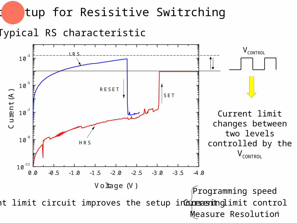
0.0 -0.5 -1.0 -1.5 -2.0 -2.5 -3.0 -3.5 -4.010-11
10-9
10-7
10-5
10-3
Cur
ent
(A)
Voltage (V)
SETRESET
LRS
HRS
Typical RS characteristic
Circuit setup for Resisitive Switrching
VCONTROL
Current limit changes between two levels
controlled by the VCONTROL
Current limit circuit improves the setup increasingProgramming speedCurrent limit controlMeasure Resolution

7
RSRTN

8
Ultra fast setup for Resisitive Switrching
1,5 2,0 2,5 3,0
10µ
100µ
1m
Curr
ent (A
)
Voltage (V)
4,0 4,5 5,0 5,5 6,0 6,5 7,0 7,5 8,0
1µ
10µ
100µ
1m
Curr
ent (A
)
Time (ms)
Ultra fastcapture
2 3 4 5
100n
1µ
10µ
100µ
Cur
rent
(A
)
Voltage (V)
0 5 10 15 20 25
100n
1µ
10µ
100µ
Cur
rent
(A
)
Time (ms)
Ultra fastcapture
Circuit allows ultra fast measures and applies the current limit during SET process.
Circuit allows ultra fast measures and applies the current limit during SET process.

9
0 0.05 0.1 0.15 0.2 0.25 0.3 0.35 0.4 0.45 0.510
-11
10-10
10-9
10-8
10-7
10-6
10-5
10-4
0 0.05 0.1 0.15 0.2 0.25 0.3 0.35 0.4 0.45 0.5-1
0
1
2
3
4
5
6
7
8
9
Ultra fast setup with pulses
0 0.05 0.1 0.15 0.2 0.25 0.3 0.35 0.4 0.45 0.510
-12
10-10
10-8
10-6
10-4
10-2
0 0.05 0.1 0.15 0.2 0.25 0.3 0.35 0.4 0.45 0.5-0.5
0
0.5
1
1.5
2
2.5
3
3.5
4
SET
RESET
More and faster cycles. Allows endurance sample studies.
Improves Semiconductor Analyzer setup.

10
Random Telegraph Noise RTN
0.00 0.05 0.1020
40
60
time (s)
Curr
ent (
nA
)
RTN introduces variability to the RS States, specially during HRS.
RTN during HRS
Top Electrode
Bottom Electrode
Vstress“Traps”
RTN is due to changes in the filament structure
Device Array High Density Array
Variability

11
RS Cycling
RTN measurement with semiconductor parameter analyzer (SPA)
oscilloscopeRTN capture
End of SPA measurement
Time Scale Change
Yes
No
New RTN measurement
Ultra fast setup for RTN
Poor sampling resolution
Ultra fast capture

12
0 200 400 600 800 10000
100200300400500
Curr
ent (n
A)
Time (s)
V=2.1V
0,00 0,05 0,10 0,15 0,20
1E-7
1E-6
Curr
ent (n
A)
Time (s)
46.8 47.0 47.2 47.4 47.621
28
35
Curr
ent (n
A)
time (s)
0.00 0.05 0.1020
40
60
time (s)
Curr
ent (
nA
)
SMU
Scope Scope
RS Cycling
RTN measurement with semiconductor parameter analyzer (SPA)
oscilloscopeRTN capture
End of SPA measurement
Time Scale Change
Yes
No
New RTN measurement Ultra fast setup for RTN
Osciloscope captures by GPIB interruptions

13
0.00 0.02 0.04 0.06 0.08 0.10
240.0
280.0
320.0
360.0
0.00 0.01 0.02 0.03 0.04 0.05
200.0
220.0240.0
260.0
280.0
0.0000 0.0005 0.0010 0.0015 0.0020 0.0025
200.0
220.0240.0
260.0
280.0
Cur
rent
(nA
)
Osc. time window (s)
6.7msa) Time Res.= 40s
L3
L6
L1L6
L10
Time Res.= 20sb)
Cur
rent
(nA
)
Osc. time window (s)
1.84ms
L7
L5
L10
L6Time Res.= 1sc)
Cur
rent
(nA
)
Osc. time window (s)
200s
(a) 7.26s and 9.68s with 40µs time resolution.
(b) 9.68s and 12.15s with 20µs time resolution.
(c) 19.5s and 21.93s with 1µs time resolution.
Ultra fast setup for RTN
Different time window length

Weighted Time Lack Method/Plot
More likely due to defect fluctuations in the filament, caused by stochastic atomic movements in and out of the CFs.
VG=-0.11V
current at i
curr
ent
at
i+1
0.8 1 1.2 1.4 1.6
x 10-9
0.8
1
1.2
1.4
1.6
x 10-9
0 200 400 600 800 1000 12000.6
0.8
1
1.2
1.4
1.6
1.8x 10
-9 VG=-0.11V
Time (s)
I (A
)
0.5 1 1.5 2
x 10-9
0.5
1
1.5
2x 10
-9 VG=-0.11V
Top Electrode
Bottom Electrode
Vstress“Traps”
Filament Conductivity Fluctuations
WTLPcapture
14

15
0 5 10 15 20 25 30 35 40 45
160,0n
180,0n
200,0n
220,0n
240,0n
260,0n
280,0n
300,0n
320,0n
340,0n
1 0,1 0,01
160,0
180,0
200,0
220,0
240,0
260,0
280,0
300,0
320,0
340,0
Curr
ent (
A)
time (s)
L9
L8
L7
L6
L5
L4
L2
L3
Curr
ent (
nA
)
WTLP Diag. (a.u.)
L1
(Left) Typical multilevel RTN signal measured by a semiconductor parameter analyzer at Vapp=1.25V, step time ~6ms and number of measured points 8000.
(Right) Trap levels obtained by using the WTLP method.
Weighted Time Lack Method

16
Weighted Time Lack Plot16
0.0
200.
0
240.
0
280.
0
320.
0
160.0
180.0
200.0
220.0
240.0
260.0
280.0
300.0
320.0
340.0
L10
L2
L3
L4
L5L6
L7
L8L9
Cur
rent
at i
+1
(nA
)
L1a)
160.
0
200.
0
240.
0
280.
0
320.
0
L1
L6
L3
b)
Time Res.=40s
160.
0
200.
0
240.
0
280.
0
320.
0
L10
L7
L6
c)
Time Res.=20s
160.
0
200.
0
240.
0
280.
0
320.
0
L5
L10
-3.500
-2.800
-2.100
-1.400
-0.7000
0
L6
Current at i (nA)
Time Res.=1s
d) WTLP (a.u.)
WTLP method applied to
(a) RTN measured by the SPA with 9 trap levels detected.(b) Oscilloscope capture with a time resolution of 40μs where 3 trap levels detected.(c) Oscilloscope capture with time resolution of 20μs with 3 trap levels detected.(d) Oscilloscope capture at lower time resolution of 1μs with 2 trap levels.
More resolution of de Weighted Time Lack Plot with ultra fast captures
Fast emission and capture times not detected with SPA setup

17
0,00 0,05 0,10 0,15 0,20
1E-7
1E-6
Curr
ent (n
A)
Time (s)
Tools for RTN characterization
Weighted Time Lag Method Ultra fast characterization
Measuring capture and emission timeStudy variability of Resistive Switching states
Extract statistics of RTN variability for modeling
The combination of both tools allows:

18
CIRCUIT LEVEL

19
Variability sources.
Electrically minimize variability.
Variability analysis on circuit performance.
Circuit Level: Objectives
Reliability issues
Architectures
Cross point structures based on RS cells.

20
RTN and RS modeling
Electrical model.
RS state represented by R value.
Bipolar RS.
Potential law for RS currents.
Easy transfer to circuit level.
RS electrical model
Diode – Resistance model
Circuit level simulations
Including variability
Statistical models

21
Resistive Switching variability
1 10 100 10001E-11
1E-10
1E-9
1E-8
1E-7
1E-6
1E-5
1E-4
ESET
ERESET
Ene
rgy
(J)
Ramp Speed (V/s)
Energy Average
0 50 100 150 200 250 300 3501E-12
1E-11
1E-10
1E-9
1E-8
1E-7
1E-6
1E-5
1E-4
1E-3
0.01
0.1
IBD @ -0.5V
IR @ -0.5V
|Co
rrie
nte
de
pu
ert
a [
A]|
Ciclos
HBD
SBD
Estado BD
-5 -4 -3 -2 -10.1
1
10
40
70
95
99.5
Pro
ba
bili
da
d [
%]
Tensión de puerta [V]
VBD
VR
ciclos iniciales
RS CurrentProgramming voltages
Programming consumption VARIABILITY
0.00 0.05 0.1020
40
60
time (s)
Cur
rent
(nA
)RTN

22
Resistive Switching variability
1 10 100 10001.5
2.0
2.5
3.0
3.5
4.0
4.5
5.0
5.5
VSET
VRESET
Vol
tage
(V
)
Ramp Speed (V/s)
Voltage Average of last 4
Programming voltage window increases as speed programming increases
-2 0 2 4 6 8 10 12 1410
-13
10-12
10-11
10-10
10-9
10-8
10-7
10-6
10-5
10-4
10-3
-0.5 0 0.5 1 1.5 2 2.5 3 3.5 4 4.510
-12
10-10
10-8
10-6
10-4
10-2
100
-2 0 2 4 6 8 10 12 1410
-13
10-12
10-11
10-10
10-9
10-8
10-7
10-6
10-5
10-4
10-3
-0.5 0 0.5 1 1.5 2 2.5 3 3.5 4 4.510
-12
10-10
10-8
10-6
10-4
10-2
100
VSET
VRESET
Programming speed

23
Resistive Switching variability
Current limit
1E-10 1E-8 1E-6 1E-4
1
10
40
70
95
99.5
IR @-0.5V
IBD @-0.5V
Pro
babili
dad (
%)
|Corriente de puerta [A]|
-4.5 -4.0 -3.5 -3.0 -2.5
-7-6-5-4-3-2-10123
Distribución de IBD
Ln(-
Ln(1
-F))
Log_10(Corriente de puerta [A])
CL=2mA CL=1mA CL=0.5mA
(a)
-12 -11 -10 -9 -8 -7 -6 -5 -4
-7
-6
-5
-4
-3
-2
-1
0
1
2
3
Ln(-
Ln(1
-F))
Log_10(Corriente de puerta [A])
CL = 2mA CL = 1mA CL = 0.5mA
Distribución de IR
(b)
Current limit favors HBD
LRS more stable

24
Tools for variability and circuit performance analysis.
RS and RTN characterization
Electrical and statistical models
Pspice Electrical models Easy link with circuits
Simulink Statistical parameters Equation models (QPC) High density circuits simulation
0,0 -0,5 -1,0 -1,5 -2,0 -2,5 -3,0 -3,5 -4,010-11
10-9
10-7
10-5
10-3
Cur
ent (A
)
Voltage (V)
SETRESET
LRS
HRS
Current Limit
Circuit performanceanalysis
RRAM crossbar
0.00 0.05 0.1020
40
60
time (s)
Cur
rent
(nA
)
HighDensity
Array
Device
Programming voltages
Current levels
Variability
RTN fluctuations
ERROR

25
RS based cells for crosspoints
Crosspoint structure
MOSFET based cell
Simple RS cell
MOSFET based cell
Any suggestions..?

26
Thanks!!

27
ANNEX

28
VOUT
VBULK
VSTRESS
VDUT
DUT
Current Limit Control
Buffer
I-V converter
VC controls the channel current of T1, that means the current limit of the DUT
Current limit applied by a transistor
D2
Ultra fast setup: The circuit...
Top Related